Embed Size (px)
Citation preview
1www.fciconnect.com TRX10GVP2010 Datasheet, Rev. B04, July 2010
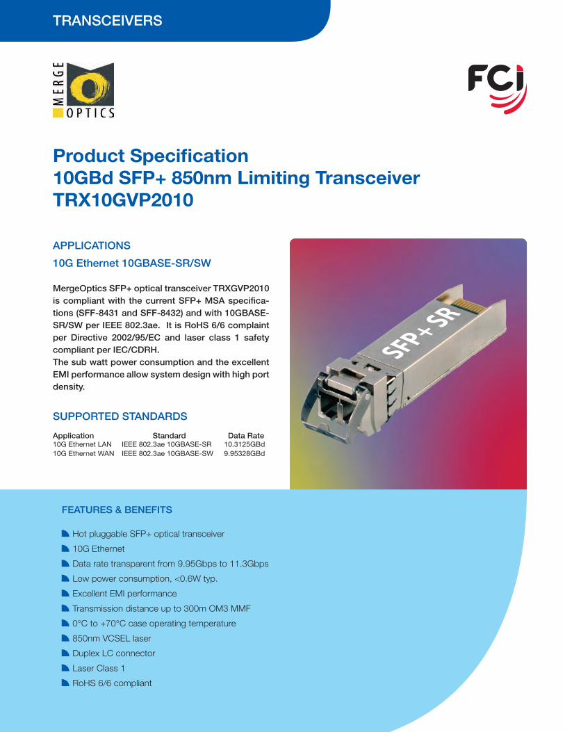
TRANSCEIVERS
Product Specification10GBd SFP+ 850nm Limiting TransceiverTRX10GVP2010
APPLICATIONS
10G Ethernet 10GBASE-SR/SW
MergeOptics SFP+ optical transceiver TRXGVP2010 is compliant with the current SFP+ MSA specifica-tions (SFF-8431 and SFF-8432) and with 10GBASE-SR/SW per IEEE 802.3ae. It is RoHS 6/6 complaint per Directive 2002/95/EC and laser class 1 safety compliant per IEC/CDRH. The sub watt power consumption and the excellent EMI performance allow system design with high port density.
SUPPORTED STANDARDS
Application Standard Data Rate10G Ethernet LAN IEEE 802.3ae 10GBASE-SR 10.3125GBd10G Ethernet WAN IEEE 802.3ae 10GBASE-SW 9.95328GBd
FEATURES & BENEFITS
Hot pluggable SFP+ optical transceiver
10G Ethernet
Data rate transparent from 9.95Gbps to 11.3Gbps
Low power consumption, <0.6W typ.
Excellent EMI performance
Transmission distance up to 300m OM3 MMF
0°C to +70°C case operating temperature
850nm VCSEL laser
Duplex LC connector
Laser Class 1
RoHS 6/6 compliant
2www.fciconnect.com TRX10GVP2010 Datasheet, Rev. B04, July 2010
TABLE OF CONTENTS
Table of Contents 2
Functional Description 3
Electrical Characteristics 4
Absolute Maximum Ratings 4
Recommended Operating Conditions 4
Low Speed Characteristics 4
SFI Module Transmitter Input Characteristics 5
SFI Module Receiver Output Characteristics 5
Optical Characteristics 6
General Parameters 6
Optical Transmitter 6
Optical Receiver 6
Application Information 7
Connector Pinout 7
Electrical Pin Definition 7
Application Schematics 8
Interfacing the Transceiver 9
Digital Optical Monitoring 9
Module Outline 10
Ordering Information 10
Related Information & Compliance 11
Eye Safety 11
Sales Contacts 12
Product Specification10GBd SFP+ 850nm Limiting Transceiver TRX10GVP2010
3www.fciconnect.com TRX10GVP2010 Datasheet, Rev. B04, July 2010
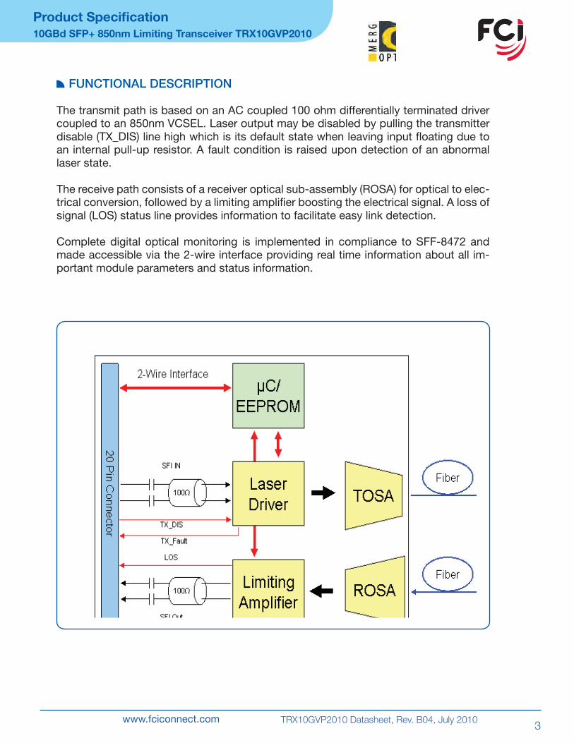
FUNCTIONAL DESCRIPTION
The transmit path is based on an AC coupled 100 ohm differentially terminated driver coupled to an 850nm VCSEL. Laser output may be disabled by pulling the transmitter disable (TX_DIS) line high which is its default state when leaving input floating due to an internal pull-up resistor. A fault condition is raised upon detection of an abnormal laser state.
The receive path consists of a receiver optical sub-assembly (ROSA) for optical to elec-trical conversion, followed by a limiting amplifier boosting the electrical signal. A loss of signal (LOS) status line provides information to facilitate easy link detection.
Complete digital optical monitoring is implemented in compliance to SFF-8472 and made accessible via the 2-wire interface providing real time information about all im-portant module parameters and status information.
Product Specification10GBd SFP+ 850nm Limiting Transceiver TRX10GVP2010
4www.fciconnect.com TRX10GVP2010 Datasheet, Rev. B04, July 2010
ELECTRICAL CHARACTERISTICS
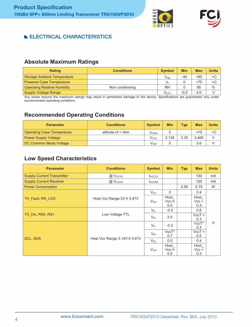
Absolute Maximum Ratings
Rating Conditions Symbol Min Max Units
Storage Ambient Temperature ϑstg -40 +85 ∞C
Powered Case Temperature ϑc 0 +75 ∞C
Operating Relative Humidity Non condensing RH 0 95 %
Supply Voltage Range VCC3 -0.5 4.0 V
Any stress beyond the maximum ratings may result in permanent damage to the device. Specifications are guaranteed only under recommended operating conditions.
Recommended Operating Conditions
Parameter Conditions Symbol Min Typ Max Units
Operating Case Temperature altitude of < 3km ϑCase 0 +70 ∞C
Power Supply Voltage VCC3 3.135 3.30 3.465 V
DC Common Mode Voltage VCM 0 3.6 V
Low Speed Characteristics
Parameter Conditions Symbol Min Typ Max Units
Supply Current Transmitter @ VCCTX IVCCTX 100 mA
Supply Current Receiver @ VCCRX IVCCRX 120 mA
Power Consumption 0.55 0.75 W
TX_Fault, RX_LOS Host Vcc Range 2V ñ 3.47V
VOL 0 0.4
V
VOH
Host_Vcc ñ
0.5
Host_Vcc +
0.3
TX_Dis, RS0, RS1 Low Voltage TTL
VIL -0.3 0.8
VIH 2.0VccT +
0.3
SCL, SDA Host Vcc Range 3.14V ñ 3.47V
VIL -0.3VccT*
0.3
VIHVccT*
0.7VccT +
0.5
VOL 0.0 0.4
VOH
Host_Vcc ñ
0.5
Host_Vcc +
0.3
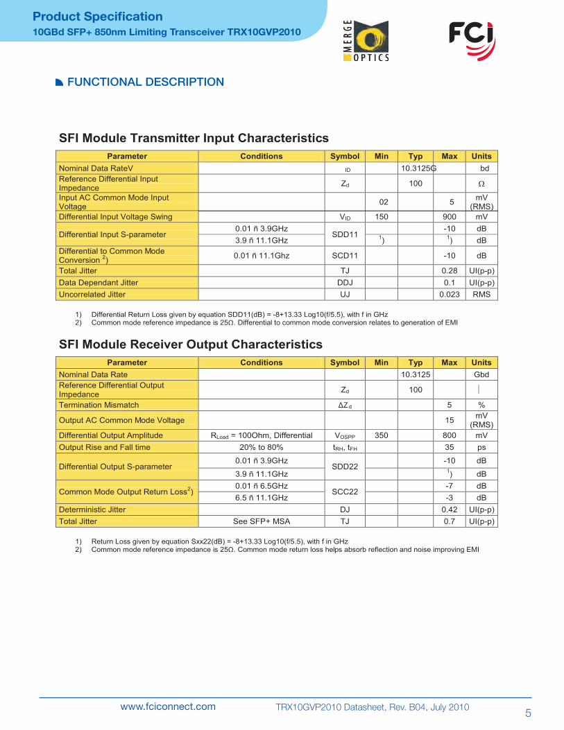
SFI Module Transmitter Input Characteristics
Parameter Conditions Symbol Min Typ Max Units
Nominal Data Rate VID 10.3125 Gbd
Reference Differential Input Impedance
Zd 100 Ω
Input AC Common Mode Input Voltage
0 25mV
(RMS)
Product Specification10GBd SFP+ 850nm Limiting Transceiver TRX10GVP2010
5www.fciconnect.com TRX10GVP2010 Datasheet, Rev. B04, July 2010
FUNCTIONAL DESCRIPTION
SFI Module Transmitter Input CharacteristicsParameter Conditions Symbol Min Typ Max Units
Nominal Data RateV ID 10.3125G bdReference Differential Input Impedance Zd 100 Ω
Input AC Common Mode Input Voltage 02 5 mV
(RMS)Differential Input Voltage Swing VID 150 900 mV
Differential Input S-parameter0.01 ñ 3.9GHz
SDD11-10 dB
3.9 ñ 11.1GHz1)
1) dB
Differential to Common Mode Conversion
2)
0.01 ñ 11.1Ghz SCD11 -10 dB
Total Jitter TJ 0.28 UI(p-p)
Data Dependant Jitter DDJ 0.1 UI(p-p)
Uncorrelated Jitter UJ 0.023 RMS
1) Differential Return Loss given by equation SDD11(dB) = -8+13.33 Log10(f/5.5), with f in GHz2) Common mode reference impedance is 25 . Differential to common mode conversion relates to generation of EMI
SFI Module Receiver Output Characteristics
Parameter Conditions Symbol Min Typ Max Units
Nominal Data Rate 10.3125 Gbd
Reference Differential Output Impedance
Zd 100
Termination Mismatch d 5 %
Output AC Common Mode Voltage 15mV
(RMS)
Differential Output Amplitude RLoad = 100Ohm, Differential VOSPP 350 800 mV
Output Rise and Fall time 20% to 80% tRH, tFH 35 ps
Differential Output S-parameter0.01 ñ 3.9GHz
SDD22-10 dB
3.9 ñ 11.1GHz1) dB
Common Mode Output Return Loss2)
0.01 ñ 6.5GHzSCC22
-7 dB
6.5 ñ 11.1GHz -3 dB
Deterministic Jitter DJ 0.42 UI(p-p)
Total Jitter See SFP+ MSA TJ 0.7 UI(p-p)
1) Return Loss given by equation Sxx22(dB) = -8+13.33 Log10(f/5.5), with f in GHz2) Common mode reference impedance is 25 . Common mode return loss helps absorb reflection and noise improving EMI
Product Specification10GBd SFP+ 850nm Limiting Transceiver TRX10GVP2010
6www.fciconnect.com TRX10GVP2010 Datasheet, Rev. B04, July 2010
OPTICAL CHARACTERISTICS
General Parameters
Parameter ConditionsMin Modal Bandwidth(MHz*km)
Symbol MinTypical1GBd
Typical10GBd
Units
Operating Range
62.5 µm MMF50 µm MMF62.5 µm MMF50 µm MMF50 µm MMF
160400200500
2000
lOP
22
0.50.50.5
220500275550X
26663382
300
m
Optical Transmitter
Parameter Conditions Symbol Min Typ Max Units
Nominal Wavelength λTRP 840 850 860 nm
Spectral Width ∆λ 0.45
Average Launch Power Pavg -7.3 -1 dBm
Extinction Ratio ER 3.5 dB
Relative Intensity Noise RIN -128 dB/Hz
Optical Receiver
Parameter Conditions Symbol Min Typ Max Units
Maximum Input Power PMAX -1 dBm
Center Wavelength λC 840 850 860 nm
Receiver SensitivityPRBS 2
31-1, BER < 1*10
-12
@10.3125GBdPIN(OMA) -11.1 dBm
Stressed Receiver SensitivityPRBS 2
31-1, BER < 1*10
-12
@ 10.3125GBdPIN(OMA) -7.5 dBm
Loss of SignalPav_as -30
dBmPOMA_deas -13
Note: The specified characteristics are met within the recommended range of operating. Unless otherwise noted typical data are quoted at nominal voltages and +25∞C ambient temperature.
Product Specification10GBd SFP+ 850nm Limiting Transceiver TRX10GVP2010
7www.fciconnect.com TRX10GVP2010 Datasheet, Rev. B04, July 2010
APPLICATION INFORMATION
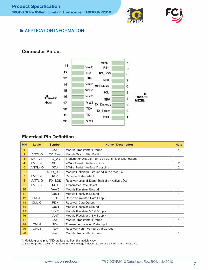
Connector Pinout
Electrical Pin Definition
PIN Logic Symbol Name / Description Note
1 VeeT Module Transmitter Ground 1
2 LVTTL-O TX_Fault Module Transmitter Fault
3 LVTTL-I TX_Dis Transmitter Disable; Turns off transmitter laser output
4 LVTTL-I SCL 2-Wire Serial Interface Clock 2
5 LVTTL-I/O SDA 2-Wire Serial Interface Data Line 2
6 MOD_DEF0 Module Definition, Grounded in the module
7 LVTTL-I RS0 Receiver Rate Select
8 LVTTL-O RX_LOS Receiver Loss of Signal Indication Active LOW
9 LVTTL-I RS1 Transmitter Rate Select
10 VeeR Module Receiver Ground 1
11 VeeR Module Receiver Ground 1
12 CML-O RD- Receiver Inverted Data Output
13 CML-O RD+ Receiver Data Output
14 VeeR Module Receiver Ground 1
15 VccR Module Receiver 3.3 V Supply
16 VccT Module Receiver 3.3 V Supply
17 VeeT Module Transmitter Ground 1
18 CML-I TD- Transmitter Inverted Data Input
19 CML-I TD+ Receiver Non-Inverted Data Output
20 VeeT Module Transmitter Ground 1
1. Module ground pins GND are isolated from the module case.2. Shall be pulled up with 4.7K-10Kohms to a voltage between 3.15V and 3.45V on the host board.
Product Specification10GBd SFP+ 850nm Limiting Transceiver TRX10GVP2010
8www.fciconnect.com TRX10GVP2010 Datasheet, Rev. B04, July 2010
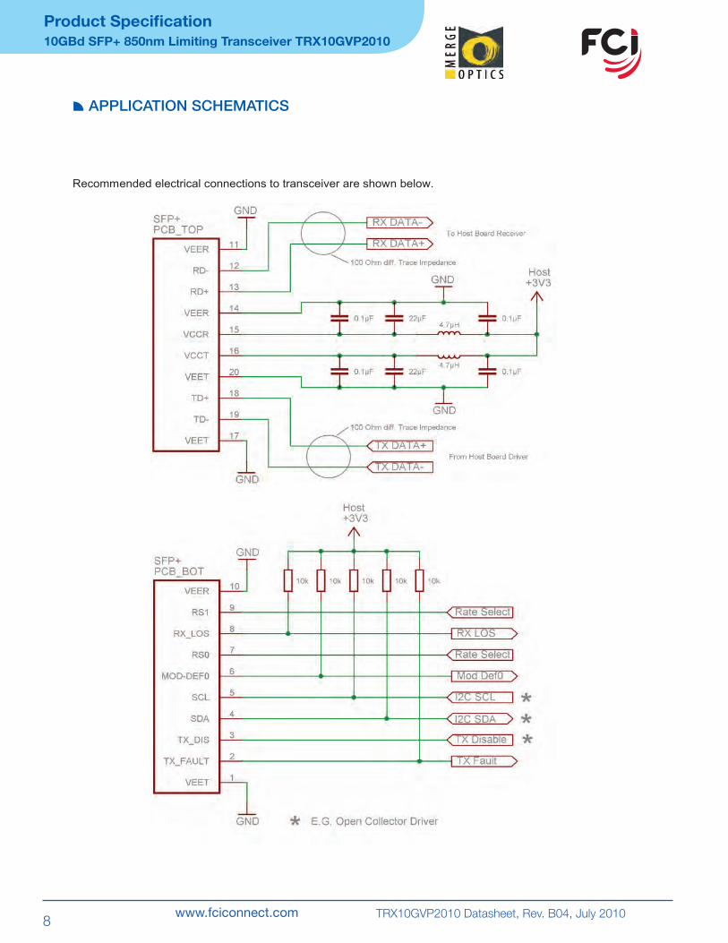
APPLICATION SCHEMATICS
Recommended electrical connections to transceiver are shown below.
Product Specification10GBd SFP+ 850nm Limiting Transceiver TRX10GVP2010
9www.fciconnect.com TRX10GVP2010 Datasheet, Rev. B04, July 2010
INTERFACING THE TRANSCEIVER
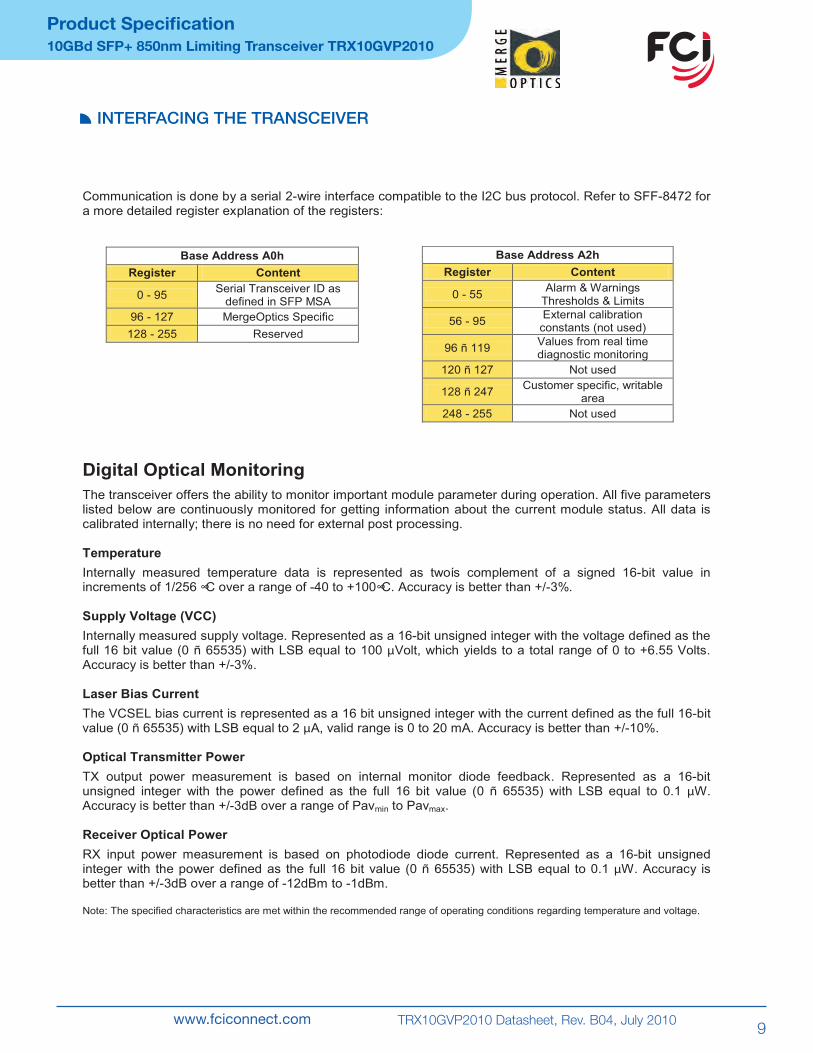
Communication is done by a serial 2-wire interface compatible to the I2C bus protocol. Refer to SFF-8472 fora more detailed register explanation of the registers:
Base Address A0h
Register Content
0 - 95Serial Transceiver ID as
defined in SFP MSA
96 - 127 MergeOptics Specific
128 - 255 Reserved
Digital Optical Monitoring
The transceiver offers the ability to monitor important module parameter during operation. All five parameters listed below are continuously monitored for getting information about the current module status. All data is calibrated internally; there is no need for external post processing.
Temperature
Internally measured temperature data is represented as twoís complement of a signed 16-bit value in increments of 1/256 ∞C over a range of -40 to +100∞C. Accuracy is better than +/-3%.
Supply Voltage (VCC)
Internally measured supply voltage. Represented as a 16-bit unsigned integer with the voltage defined as the full 16 bit value (0 ñ 65535) with LSB equal to 100 Volt, which yields to a total range of 0 to +6.55 Volts.Accuracy is better than +/-3%.
Laser Bias Current
The VCSEL bias current is represented as a 16 bit unsigned integer with the current defined as the full 16-bit value (0 ñ 65535) with LSB equal to 2 A, valid range is 0 to 20 mA. Accuracy is better than +/-10%.
Optical Transmitter Power
TX output power measurement is based on internal monitor diode feedback. Represented as a 16-bit unsigned integer with the power defined as the full 16 bit value (0 ñ 65535) with LSB equal to 0.1 W. Accuracy is better than +/-3dB over a range of Pavmin to Pavmax.
Receiver Optical Power
RX input power measurement is based on photodiode diode current. Represented as a 16-bit unsigned integer with the power defined as the full 16 bit value (0 ñ 65535) with LSB equal to 0.1 W. Accuracy is better than +/-3dB over a range of -12dBm to -1dBm.
Note: The specified characteristics are met within the recommended range of operating conditions regarding temperature and voltage.
Base Address A2h
Register Content
0 - 55Alarm & Warnings
Thresholds & Limits
56 - 95External calibration
constants (not used)
96 ñ 119Values from real time diagnostic monitoring
120 ñ 127 Not used
128 ñ 247Customer specific, writable
area
248 - 255 Not used
Product Specification10GBd SFP+ 850nm Limiting Transceiver TRX10GVP2010
10www.fciconnect.com TRX10GVP2010 Datasheet, Rev. B04, July 2010
Product Specification10GBd SFP+ 850nm Limiting Transceiver TRX10GVP2010
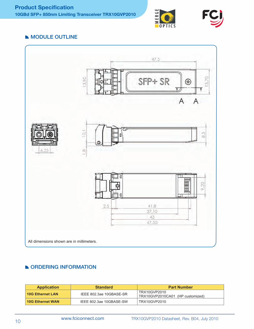
MODULE OUTLINE
ORDERING INFORMATION
All dimensions shown are in millimeters.
11www.fciconnect.com TRX10GVP2010 Datasheet, Rev. B04, July 2010
Product Specification10GBd SFP+ 850nm Limiting Transceiver TRX10GVP2010
RELATED INFORMATION & COMPLIANCE
EYE SAFETY
Requirements Standard
RoHS RoHS 6/6 Directive 2002/95/ECAmendment 4054 (2005/747/EC)
EMI (Module)FCC Part 15, Class B
EN 55022 Class BCISPR 22
Requirements Standard Value
ESD (Electrical connector) JEDEC JESD22-A114-B 1kV
ESD (Module case) Air DischargeEN61000-4-2 criterion B 15kV
ESD (Module case) Contact DischargeEN61000-4-2 criterion B 8kV
This laser based multimode transceiver is a Class 1p roduct. It complies with IEC 60825-1 Edition 2 and FDA performance standards for laser products (21 CFR 1040.10 and 1040.11) except for deviations pursuant to Laser Notice 50, dated July 26, 2001.
CLASS 1L ASER PRODUCT
To meet laser safety requirements the transceiver shall be operated within the Absolute Maximum Ratings.
Note: All adjustments have been made at the factory prior to shipment of the devices. No maintenance or alteration to the device is required. Tampering with or modifying the performance of the device will result in voided p roduct w arranty. F ailure t o adhere t o the above restrictions c ould r esult in a m odification that i s considered an act of “manufacturing”, and will require, under law, recertification of the modified product with the U.S. Food and Drug Administration (ref. 21 CFR 1040.10 (i)).
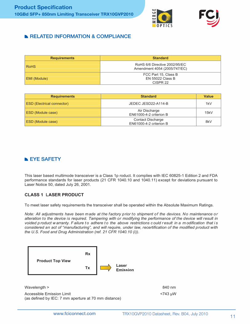
Wavelength > 840 nm
Accessible Emission Limit(as defined by IEC: 7 mm aperture at 70 mm distance)
<743 µW
Product Top View
Rx
Tx Laser Emission
1L

12www.fciconnect.com TRX10GVP2010 Datasheet, Rev. B04, July 2010
For more information about e-catalog or FCIsales offices, headquarters, agents and local distributors,
visit www.fciconnect.com
EUROPE
FCI Deutschland GmbH
Wernerwerkdamm 16 13629 Berlin, Germany Ph: +49 30 750 795 00 Fax: +49 30 386 37 54
AMERICAS
MergeOptics 1551 McCarthy Blvd, Suite 116 Milpitas, CA 95035 USA Phone: 408-493-9970
More information about FCI’s complete range of High Speed Input/Output products can be found on www.fciconnect.com/hsio
Contact info
ELX
10G
VP
2010
710E
LT
Prin
ted
on
recy
cled
pap
er