Embed Size (px)
Citation preview

JPL Publication 89-1J
J
Product Assurance Technology forProcuring Reliable, Radiation-Hard,Custom LSI/VLSI Electronics
Report for Period"October 1984 - September 1986
M. G. BuehlerR. A. Allen
B. R. Blaes
K. A. Hicks
G. A. JenningsY.-S. LinC. A. PiSa
H. R. SayahN. Zamani
Janua_ 1989
( "! ,,--L -- '
r',"i. :_r _ t
Prepared for
Defense Advanced Research Projects Agency,U.S. Department of Defenseand
National Aeronautics and Space Administration
by
Jet Propulsion LaboratoryCalifornia Institute of Technology
Pasadena, California
LLtC T?L.P tIC :_
N 'L,-,'n2 L
https://ntrs.nasa.gov/search.jsp?R=19900010965 2018-07-17T09:12:08+00:00Z

JPL Publication 89-1
Product Assurance Technology forProcuring Reliable, Radiation-Hard,Custom LSI/VLSI Electronics
Report for Period"October 1984 - September 1986
M. G. BuehlerR. A. AllenB. R. BlaesK. A. HicksG. A. JenningsY.-S. LinC. A. PiSaH. R. SayahN. Zamani
Janua_ 1989
Prepared for
Defense Advanced Research Projects Agency,U.S. Department of Defense
and
National Aeronautics and Space Administration
by
Jet Propulsion LaboratoryCalifornia Institute of Technology
Pasadena, California

The work described in this report was performed by the Jet Propulsion
Laboratory, California Institute of Technology, and was sponsored by the De-
fense Advanced Research Projects Agency, the National Security Agency, and
the National Aeronautics and Space Administration.

Abstract
In this effort, advanced measurement methods that use microelectronic test
chips are described. These chips are intended to be used in acquiring the data
needed to qualify Application Specific Integrated Circuits (ASICs) for space
use. This work represents the collaborative effort of integrated-circuit (IC) parts
specialists, device physicists, test-chip engineers, and fault-tolerant-circuit de-
signers. Their efforts were focused on developing the technology for obtaining
custom ICs from CMOS/bulk silicon foundries. In pursuit of this goal a series
of test chips has been developed: a Parametric Test Strip, a Fault Chip, a set
of Reliability Chips, and the CRRES (Combined Release and Radiation Effects
Satellite) Chip, a test circuit for monitoring space radiation effects.
The technical accomplishments of this effort include:
1. Development of a Fault Chip that contains a set of test structures used
to evaluate the density of various process-induced defects. In addition,
procedures were developed to determine which defects are most likely to
cause failures in concurrently fabricated circuits. In the reporting period,
seven versions of the fault chip have been prepared.
2. Development of new test structures and testing techniques for measuring
gate-oxide capacitance, gate-overlap capacitance, and propagation delay.
. Development of a set of Reliability Chips that are used to evaluate failure
mechanisms in CMOS/Bulk: interconnect and contact electromigration
and time-dependent dielectric breakdown.
4. Development of MOSFET parameter extraction procedures for evaluatingsubthreshold characteristics.
, Evaluation of Test Chips and Test Strips on the second CRRES wafer
run. This data was used to analyze wafer-level test structure requirements
demonstrating that sufficient data to characterize the wafer run could be
acquired from a limited number of drop-in sites (for example, nine).
. Two dedicated fabrication runs for the CRRES Chip flight parts. Flight
parts from these runs were shipped to the CRRES program in March,
1986. Radiation tests (Total Integrated Dose and Single Event Upset)
were performed on these parts.
7. Publication of two papers: one on the Split-Cross Bridge Resistor and
another on Asymmetrical SRAM Cells for Single-Event Upset Analysis.
iii


Acknowledgements
The present address of C. A. Pifia is University of Southern California/In-
formation Sciences Institute, Marina del Rey, California and the present address
of G. A. Jennings is Department of Computer Engineering, University of Lund,
Sweden.
PRECEDING PAGE BLANK NOT FILMED PAGE,,iV INTENTf0NAH.T BLANK


Contents
1 Introduction 1
2 Test Chip Sets
2.1
2.2
5
Introduction .............................. 6
Fault Test Chip ............................ 10
2.2.1
2.2.2
2.2.3
2.2.4
2.2.5
2.2.6
2.2.7
2.2.8
2.2.9
2.2.10
2.2.11
2.2.12
2.2.13
2.2.14
2.2.15
Abstract ............................ 10
Introduction ......................... 10
Fault Chip Organization ................... 12
Pinhole Array Capacitor ................... 16
Comb/Serpentine/Cross-Bridge Resistor .......... 20
Contact Chain and Contact Chain Matrix ......... 25
Floating Gate Transistors .................. 32
Matrixed Inverters ...................... 40
Matrixed Transistors ..................... 40
Fault Chip Summary Results ................ 41
Fault Prioritization Process ................. 46
Circuit Timing Degradation due to Gate Oxide Pinholes . 48
Fault Chip Testing ...................... 50
Future Work ......................... 51
Conclusion .......................... 57
3 Test
3.1
Structures 59
Gate Oxide Capacitors ........................ 60
3.1.1
3.1.2
3.1.3
3.1.4
3.1.5
3.1.6
Introduction ......................... 60
Theory ............................ 60
Capacitor Structure Design ................. 61
Measurement Techniques .................. 64
Equipment .......................... 68
Results and Conclusions ................... 72
vii
PRECEDING PAGE BLANK NOT FILMED

..°
VIII CONTENTS
3.2 Timing Sampler Array ........................ 72
3.2.1 Introduction ......................... 72
3.2.2 Direct Measurement of Circuit Delays ........... 73
3.2.3 Muller C-Element as a Timing Sampler .......... 79
3.2.4 Data Analysis ......................... 85
3.2.5 Conclusions .......................... 90
3.3 Proximity Structures ......................... 90
3.3.1 Introduction ......................... 90
3.3.2 Structure Geometry ..................... 90
3.3.3 Experimental Results .................... 92
3.3.4 Conclusions .......................... 92
3.4 The Split-Cross-Bridge Resistor ................... 94
4 Reliability Test Structures 103
4.1 Introduction .............................. 104
4.1.1 Electromigration ....................... 104
4.1.2 Time-Dependent Dielectric Breakdown (TDDB) ..... 104
4.2 Layer Electromigration ........................ 104
4.2.1 Test Structures ........................ 104
4.2.2 Test Methods ......................... 108
4.3 Contact Electromigration ...................... 108
4.3.1 Test Structure ........................ 108
4.3.2 Test Method ......................... ll0
4.4 Time-Dependent Dielectric Breakdown ............... 110
4.4.1 Test Structure ........................ 110
4.4.2 Test Method ......................... 110
4.4.3 Analysis Method ....................... 112
4.5 Summary of Results and Future Work ............... 116
5 Device Models and Simulation 117
5.1 MOSFET Subthreshold Parameter Extraction ........... 118
5.1.1 Introduction ......................... 118
5.1.2 Subthreshold Expression ................... 123
5.1.3 Parameter Extraction Algorithms ............... 128
5.1.4 Results ............................ 129
5.1.5 Conclusions .......................... 135
5.2 Integrated Circuit Simulation on the Hypercube ......... 135
5.2.1 Objectives ........................... 135
5.2.2 Progress and Results ..................... 136

CONTENTS ix
5.2.3
5.2.4
5.2.5
Significance of the Results .................. 136
Personnel ........................... 137
Publications .......................... 137
6 A Test Ch'p Case Study
6.1
6.2
6.3
6.4
6.5
6.6
6.7
6.8
6.9
6.10
6.11
139
Introduction .............................. 140
Areas of Investigation ........................ 140
Test Chip and Test Strip Design .................. 144
Geometry and Test Program Generation .............. 144
Wafer Probing and Disposition of Data .............. 146
Test Strip Wafer Map Preliminary Results ............. 147
Parametric Test Strip Probing ................... 147
Wafer Map Comparisons ....................... 158
Mean Value Comparisons ...................... 161
Mean Value Comparisons: Summary Results ........... 161
Wafer Maps .............................. 165
7 CRRES Project
7.1
7.2
7.3
7.4
7.5
7.6
7.7
7.8
7.9
7.10
171
Introduction .............................. 172
Purpose ................................ 172
CRRES Chip Description ...................... 172
SRAM ................................. 182
1986 NSREC Paper ......................... 190
MOSFET Matrix ........................... 195
Timing Sampler ............................ 197
7.7.1 Test Hardware and Measurement Procedure ........ 204
7.7.2 Data and Results ....................... 205
7.7.3 Conclusions .......................... 210
Conclusions .............................. 213
Future Work ............................. 213
CRRES Chip Test Configuration Pin Outs ............. 214
Bibliography 223


List of Figures
2.1
2.2
2.3
2.4
2.5
2.5
2.6
2.6
2.7
2.8
2.9
2.10
2.11
2.12
2.13
2.14
2.15
2.16
2.17
2.18
2.19
2.20
2.21
2.22
2.23
2.24
2.25
Fault Chip No. 5 ........................... 13
Fault Chip No. 7 ............................ 15
Gate Oxide defect origin ....................... 17
Two types of Pinhole Array Capacitor (PAC) structures ..... 18
P-PAC test results for run M44E, wafer 4 ............. 21
P-PAC test results for run M44E, wafer 4 (Continued) ....... 22
N-PAC test results for run M44E, wafer 4 ............. 23
N-PAC test results for run M44E, wafer 4 (Continued) ...... 24
First-Layer Metal Comb/Serpentine/Cross-Bridge Resistor 26
Schematic diagram of the Comb/Serpentine Resistor ....... 27
Run M61P Poly Comb/Serpentine/Cross-Bridge test results . 28
Contact Chain Structure ....................... 29
Contact Chain Matrix Structure (Layout) ............. 30
Contact Chain Matrix Structure (Schematic) ........... 31
Contact resistance probability analysis method .......... 32
M62Z contact probability analysis p+Poly/Metal contacts .... 33
Floating gate transistor models ................... 34
Test setup for floating gate transistors ............... 35
Floating-Gate device analysis .................... 36
Run M61P n-channel floating gate transistor analysis ....... 37
Experimental results of the gate poly overlap length variations onthe conduction state of the n-channel transistor .......... 39
Two types of the faulted inverter structure ............ 40
Transistor Matrix test circuit .................... 43
SEM Photos of M61P Metal Serpentine showing a wire break . . 44
Fault prioritization process ..................... 48
Fault models for n- and p-channel devices ............. 51
Circuit configuration and timing table used for simulating faulty
n-channel transistors ......................... 52
PRECEDING PAGE BLANK NOT FILMED
xi

xii
2.26
2.27
2.28
2.29
LIST OF FIGURES
Circuit configuration and timing table used for simulating faulty
p-channel transistors ......................... 53
Change in propagation delay of n- and p-channel transistors due
to gate oxide pinhole resistance ................... 54
Automated wafer prober and parametric data acquisition system 55
Slotted-chuck chip holder for automated chip testing ....... 56
3.1 The Annular MOSFET capacitor test structure .......... 63
3.2 The Racetrack MOSFET capacitor test structure ......... 64
3.3 Schematic of the inversion method for measuring capacitance . . 65
3.4 Cross section of an n-MOSFET while using the inversion method
for measuring capacitance ...................... 66
3.5 Inversion method Capacitance-Voltage n-MOSFET curve .... 67
3.6 Gate Capacitance-Length plot for an annular n-MOSFET mea-
sured in inversion ........................... 68
3.7 Connections to a MOSFET to perform the accumulation method
of capacitance measurement ..................... 69
3.8 The accumulation method for measuring oxide capacitance, Co_ . 70
3.9 Error introduced in the accumulation capacitance measurement
method by using different probe/matrix paths .......... 71
Traditional approach to delay measurement ............ 74
Timing sampler delay measurement ................. 76
Differential delay measurement with timing sampler ....... 77
Measuring inter-chip delay ...................... 78
Two-input Muller C-Element as a timing sampler ......... 80
Positive transition delay measurement using a C-Element .... 81
3.10
3.11
3.12
3.13
3.14
3.15
3.16
3.17
3.18
3.19
3.20
3.21
3.22
3.23
3.24
CMOS dynamic C-Element latch .................. 82
Restoring the logic level of the C-Element with a staticizer . . . 83
Block diagram of the Timing Sampler Array ............ 84
One stage of the Timing Sampler Array .............. 85
Timing sampler as-measured inverter pair data .......... 86
CMOS circuit delay calculations using a tau model ........ 86
Timing sampler array inverter chain element ........... 87
Timing sampler fitted data ..................... 89
Collision Test Structures ....................... 91
4.1 The electromigration test structure ................. 105
4.2 Cross section of part of the electromigration test structure .... 105
4.3 Electromigration structure first and second metal layers ..... 107

LIST OF FIGURES xiii
4.4 The metal-n-t-diffusion contact electromigration test structure . 109
4.5 The time-dependent dielectric breakdown structure ........ lll
5.1 The p-MOS reference case ...................... 118
5.2 The n-MOS reference case ...................... 119
5.3 Subthreshold characteristics for a p-MOSFET at radiation levels
¢2 > ¢1 ................................ 120
5.4 Subthreshold characteristics for an n-MOSFET at radiation levels
¢2 > ¢1 ................................ 121
5.5 The model of an n-MOSFET where the drain and source resis-
tance is R ............................... 122
5.6 Charge density, electric field, and electric potentials for a uni-
formly doped n-MOSFET ...................... 124
5.7 MOSFET drain characteristics for VDS = 5.0V ......... 133
5.8 MOSFET drain characteristics for VDS = 0.05V ......... 134
6.1 Four-inch diameter silicon wafer from run VTI-2 ......... 141
6.2 Map of the VTI-2 wafer ....................... 142
6.3 Test Chip wafer maps for the sheet resistance and linewidths of
the n+diffusion and p-t-diffusion from VTI 2, Wafer #10 ..... 166
6.4 Test Chip wafer maps for the sheet resistance and linewidths of
the n+poly and metal from VTI 2, Wafer #10 .......... 167
6.5 Test Chip wafer maps for the contact resistances from VTI2,
Wafer _ 10 .............................. 168
6.6 Test Chip wafer maps for the transistor threshold voltage, VTO,
and conduction factor, KP, for n- and p-channel MOSFETs... 169
6.7 Test Chip wafer maps for the inverter VINV and Gain ...... 170
7.10
7.1 The JPL CRRES Chip ........................ 173
7.2 The CRRES Satellite ......................... 175
7.3 JPL CRRES chip SRAM logic diagram .............. 177
7.4 The JPL CRRES Chip MOSFET Matrix ............. 178
7.5 Transistor locations in the MOSFET matrix ............ 179
7.6 Geometry of cells in MOSFET Matrix ............... 180
7.7 JPL CRRES Chip Timing Sampler Circuit ............ 181
7.8 Design errors in the 4 kbit SRAM cell ............... 182
7.9 Encroachment of the p-well into the p+diffusion in the transistor
matrix decoder circuitry ....................... 183
Expansion of the p-well around design boundaries in the SRAM
cell ................................... 184

xiv LIST OF FIG URES
7.11
7.12
7.13
7.14
7.15
7.16
7.17
7.18
7.19
7.20
7.21
7.22
7.23
7.24
7.25
7.26
7.27
Voiding in the interlevel oxide .................... 185
Circuit diagram of one pair of JPL CRRES Chips on the MEP 186
Symmetrical cell, lk SRAM heavy ion upset response ...... 188
Asymmetrical cell, lk SRAM heavy ion upset response ...... 189
Transistor measurement configuration ............... 196
Pre- and post-irradiation n-channel MOSFET curves ....... 198
CRRES Chip leakage versus total dose ............... 199
Threshold voltage versus dose for n- and p-channel MOSFETs 203
Timing analysis for the CRRES chip timing sampler ....... 204
Apparatus for measuring JPL CRRES chip timing sampler . . . 206
Timing sampler inverter-pair array data .............. 207
Positive edge inverter-pair delta data from one chip ........ 208
Wafer map of the average inverter-pair delay for positive edges
(Wafer 4) ............................... 211
Wafer map of the average inverter-pair delay for negative edges
(Wafer 4) ............................... 212
Test specifications for the JPL CRRES Chip SRAM ....... 216
Test specifications for the JPL CRRES Chip Timing Sampler . 218
Test specifications for the JPL CRRES Chip MOSFET Matrix 220

List of Tables
2.1
2.1
2.2
2.3
2.4
2.5
2.6
2.7
2.8
2.9
2.10
2.11
2.12
Critical parameters and associated test structures ......... 7
Critical parameters and associated test structures (Continued). 8
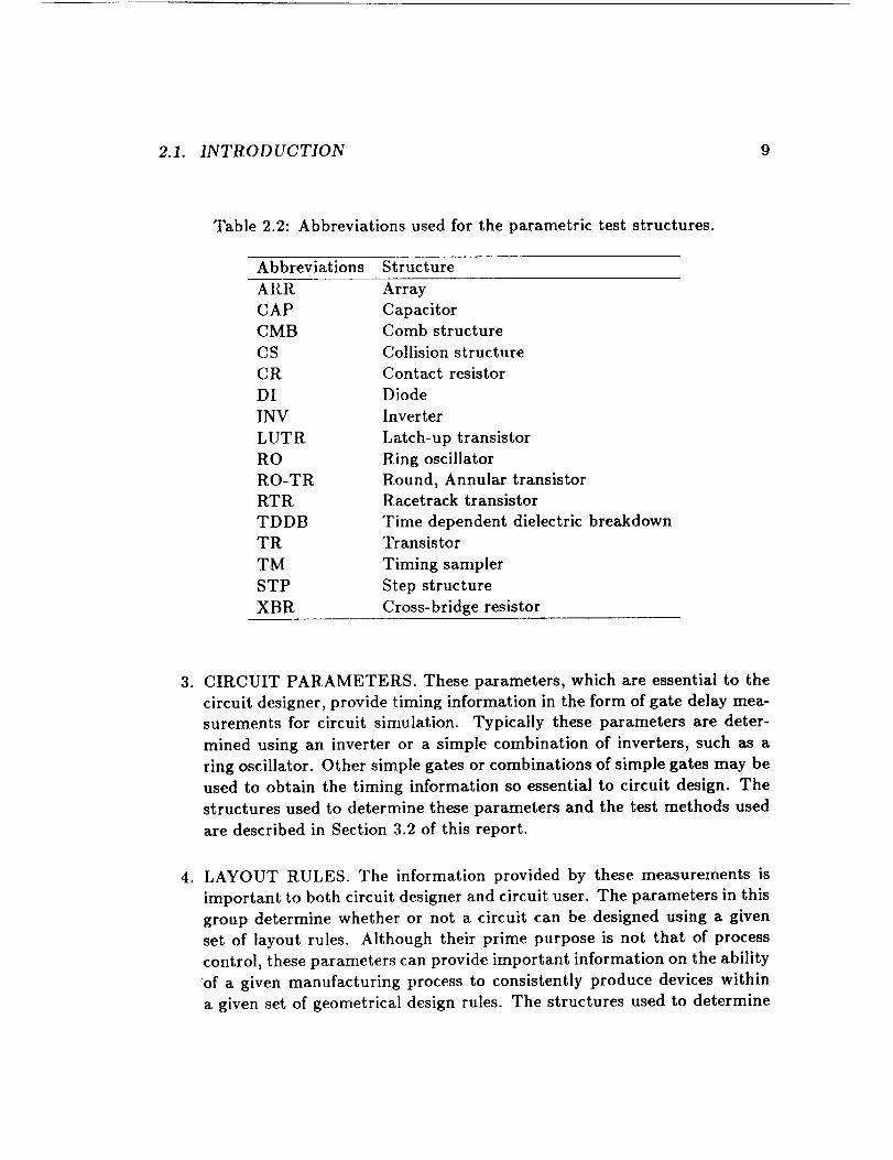
Abbreviations used for the parametric test structures ....... 9
The Fault Chip test structures and associated parameters .... 12
Test structures for Fault Chip No. 5 ................ 14
Test structures for Fault Chip No. 7 ................ 16
Pinhole Array Capacitor defect classes ............... 19
Pinhole Array Capacitor defect identification ........... 20
Fault Chip Report 1 ......................... 42
Fault Chip Report 2 ......................... 45
Fault Chip Report 3 ......................... 47
Example circuit ............................ 49
Priority listing of likely defects for the example circuit ...... 50
3.1 Results from tests of Round MOSFETs .............. 72
3.2 Diode breakdown voltages of various Collision Test Structures . 92
3.3 Design rules indicated by Collision Test Structures ........ 93
4.1 The Interconnect Electromigration Test Chip ........... 106
4.2 Dimensions of Metal Wires in Layer Electromigration Structure . 106
4.3 Examples of modeled data for the step-stress oxide breakdown
experiment .............................. 113
4.3 Examples of modeled data for the step-stress oxide breakdown
experiment (continued) ....................... 114
4.4 Results from analysis of the data in Table 4.3 ........... 115
5.1 Individual MOSFET parameters based on individually fitting four
MOSFETs ............................. 130
5.2 Individual MOSFET parameters derived from the global FET
parameters given in Table 5.3 .................... 131
XV

xvi LIST OF TABLES
5.3 Global MOSFET parameters .................... 132
6.1 Transistor Geometries ........................ 145
6.2 Metal to n+poly contact resistance histogram ........... 148
6.3 Metal layer sheet resistance histogram ............... 149
6.4 "Full" Wafer Map: Metal to n+Poly contact resistance ...... 150
6.5 "Avenue" Wafer Map: Metal to n+Poly contact resistance .... 151
6.6 Test Strip ST5102 results ...................... 154
6.6 Test Strip ST5102 results (Continued) ................ 155
7.1 Summary of CRRES/MOSIS Projects as of March, 1987 ..... 176
7.2 JPL CRRES Chip deliveries to the CRRES program ....... 180
7.3 Chip placement and expected dose rate for the MEP ....... 187
7.4 CRRES Chip Cobalt-60 Irradiation ................. 196
7.5 Comparison of n-MOSFET Matrix Test Results .......... 200
7.6 n-MOSFET Matrix Co-60 radiation test results .......... 201
7.7 p-MOSFET Matrix Co-60 radiation test results .......... 202
7.8 Summarized data from the timing samplers on four wafers .... 209

Chapter 1
Introduction

2 CHAPTER I. INTROD UCTION
The goal of this effort is to develop a product assurance methodology that will al-
low the procurement of reliable, radiation-hard, custom LSI/VLSI circuits from
silicon foundries and permit their use in critical applications such as spacecraft.
The use of test chips by integrated circuit manufacturers and customers is
widespread for they are essential for process control, for quantifying reliability
parameters, and for providing a basis for wafer acceptance. Currently, test chips
are being contemplated for use in the military standards system as a means of
evaluating the quality of a manufacturing process. This approach promises to
allow the qualification of custom and Application-Specific Integrated Circuits
(ASICs) in a timely and cost-effective manner.
This report describes a CMOS Product Assurance Technology to char-
acterize and evaluate particular foundry runs which is based on one test strip
and three test chips: the CMOS Process Monitor Test Strip used to characterize
process parameters and to extract SPICE parameters, the Fault Chip used to
analyze initial defect density and to identify the most common defect type, the
Reliability Chip used to characterize the expected long-time reliability and to
identify the expected long-time failure modes, and the CRRES Chip used to
characterize the response of the fabrication to radiation. The CRRES (Com-
bined Release and Radiation Effects Satellite) will be launched in the early 1990s.
Its Microelectronics Package (MEP) contains 12 JPL-designed chips to analyze
the effect of radiation on microelectronics. This family of structures and the
associated test methodology form the basis for integrated circuit qualification
procedures.
One key element in this methodology is the development of statistical proce-
dures to determine sample size and frequency, parameter distribution functions,
and outlier exclusion methods. This is important due to the limited area of a
wafer which is available for use for test structures. As part of this effort we de-
veloped a special test structure to measure contact resistance which allows the
statistical characterization of 464 contacts of four different types using a much
smaller area than that needed for individually probed contacts. This "smart"
test structure, incorporating row and column addressing, allows individual ac-
cess to all 464 contacts. Simulation study of the Time-Dependent Dielectric
Breakdown Structure revealed that 1600 or more test structures must be ana-
lyzed in order to minimize errors in predicting time to failure values.
Another key element in this methodology is the establishment of a parameter
data base. This allows one to compare parameter mean and standard deviation
values with those measured on previous runs, and to decide if the parameters are
on target and if the process tolerances used to characterize them are acceptable.
As part of this effort, test chips on an entire 3-#m CMOS/Bulk p-Well wafer
run were evaluated. For this particular run, the lot toleranceswere: for the gatelinewidth, 0.18 jum, for the thresholdvoltage, 0.017mV, and for the conductionfactor, 7 percent. From Cobalt 60 testing, the radiation damage factor wasfound to be about 32mV/krad(Si). In our estimation, theseare excellent valuesfor microelectronics intended for usein a natural spaceenvironment.
A final element in this methodology is the development of innovative teststructures that allow one to quickly measurekey parameters. During this pe-riod three structures of note were developed: (a) the contact resistor matrixmentioned above, (b) the gate-oxide capacitor (round and race track versions)and (c) electromigration test structures (a 15-segmentedstructure for metal,and a 16-elementstring for contact evaluations).
In order to "exercise" the product assurancetechnology,a chip wasdesignedfor the CRRES MEP and two dedicatedfoundry runs undertakenfor theseparts.On eachfoundry run ProcessMonitor Test Strips and drop-in Test Chips (con-taining a set of structures from the ProcessMonitor and the Fault Chip) wereincluded alongsidethe CRRES Chips. From the secondrun, four 3-_m CMOS p-Well waferswereanalyzed in detail. Numerousparameterswere mappedacrossthe wafers and results obtained from nine drop-ins were compared with thosefrom about 90 ProcessMonitors. This analysis led to the conclusion that ninesitesplaced in a 3 × 3 grid aresufficient to characterizethe wafer and to distin-guish acceptablewafersfrom unacceptablewafersfor current CMOS processing.
The reader is encouragedto study the following report. For those withquestions, the technical staff of the VLSI TechnologyGroup is happy to discusstechnical details and can be reachedat (818) 354-2083.

Chapter 2
Test Chip Sets
PRECEDING PAGE BLANK NOT FILMED PAGE _ INTENTIgMAI_t_BLANK

6 CHAPTER 2. TEST CHIP SETS
2.1 Introduction
As a result of the Product Assurance Technology (PAT) effort over the past
several years, a set of test structures has been developed to provide the informa-
tion required to evaluate custom or semi-custom VLSI circuits. In the conduct
of this effort, it has become evident that an efficient method that prepares the
methodology for industrial use is to develop test chips, each of which is designed
for a specific application or use. To this end, we have developed three general
families of test chips: a parametric test chip, a fault test chip and a reliability
chip. Although individual test structures can be added or deleted from these
chips if necessary, their composition is adequate to cover the CMOS critical pa-
rameter set [1]. Geometrical descriptions of these chips in Caltech Intermediate
Form (CIF) can be easily generated for different design rule sets using the JPL
Test Chip Assembler (TCA).
In this section we list the parameters needed to perform wafer or lot evalua-
tions, as well as those required to model the behavior of devices and/or circuits.
These parameters are determined from specially designed test structures. Al-
though the list of parameters is large, less than twenty morphologically different
types of test structures are needed to extract the required set. Table 2.1 lists
the critical parameters and the structures used to obtain the parameters. The
symbols for each test structure are explained in Table 2.2. The parameters are
arranged into the following six categories which were first described elsewhere
[1] and have proven to be a good classification scheme:
1. PROCESS PARAMETERS. These parameters are used to monitor the
stability of a process by measuring those parameters of a manufacturing
process that determine some of the significant process variables such as
dopant concentrations, oxide thickness, linewidth control of the different
layers, and interlayer contact resistances. Some of these same quantities
are required as inputs by the level 2 and 3 SPICE MOSFET models used
in circuit and device simulation. The structures used to determine these
parameters and the test methods used are described in the previous PAT
final report [2] and in Sections 3.1 and 3.4 of this report.
2. DEVICE PARAMETERS. The majority of these parameters are obtained
from measurements of the simplest device found in MOS circuits: the
MOSFET. The device parameters provide process control information and
are used as inputs to device and circuit simulation programs. The test
structures and test methods used to determine these parameters are de-
scribed in the previous PAT final report [2].

2.1. INTRODUCTION
Table 2.1: Critical parameters and associated test structures.
Parameters Test Structure Abbreviation
1. Process Parameters
1.1 Layer Sheet Resistance
1.2 Layer Linewidth
1.3 Metal-Layer Contact Resistance
1.4 Oxide Thickness
1.5 Substrate Dopant Density
1.6 Field Oxide Threshold Voltage
1.7 Layer-layer Alignment
1.8 Junction Breakdown Voltage
1.9 Bulk Resistivity
1.10 Bulk Lifetime
1.11 Gate Oxide Breakdown
Device Parameters
2.1 VTO (Threshold Voltage)
2.2 Gamma (Body Effect Factor)
2.3 KP (Conduction Factor)
2.4 WE (Effective Channel Width)
2.5 LE (Effective Channel Length)
2.6 Lambda (Channel Length Modulation)
2.7 IDSO (Channel Leakage Current)
2.8 IDBLEAK (Source-Drain Diode Leakage)
2.9 VDBBD (Source-Drain Diode Breakdown)
2.10 CGSO (Gate-Source Capacitance)
2.11 CGBO (Gate-Body Capacitance)
2.12 CGDO (Gate-Drain Capacitance)
2.13 CJ (Junction Capacitance)
2.14 MJ (Exponential Factor)
2.15 CJSW (Junction Sidewall Capacitance)
2.16 MJSW (CJSW Exponential Factor)
2.17 VPT (Punch-through Voltage)
2.18 VBG (Gate-Oxide Breakdown Voltage)
.
XBR
XBR, SXBR
CR, CR-ARR
CAP, RO-TR
CAP, TR
TR
ALI
TR, DI
PFPR
DI, CAP
CAP
TR
TR
TR
TR
TR
TR
TR
TR
TR
RTR-TR, ROTR
RTR-TR, ROTR
RTR-TR, ROTR
RTR-DI-
RTR-DI
RTR-DI
RTR-DI
TR
CAP

8 CHAPTER 2. TEST CHIP SETS
Table 2.1: Critical parameters and associated test structures (Continued).
Parameters
3: Circuit Parameters
Test Structure Abbreviation
6,
3.1 VH (Inverter VHIGH)
3.2 VL (Inverter VLOW)
3.3 VINV (Inverter VIN -- VOUT)
3.4 GAIN (Inverter Gain)
3.5 VNM (Inverter Noise Margin)
3.6 Tau (Gate Delay)
4. Layout Rules
4.1 Layer Linewidth
4.2 Layer Spacing4.3 Contact Size
4.4 Poly Gate Extension Over Field Oxide
4.5 Metal Overlap of Contact
4.6 Active Area Overlap Of Contact
5. Defect Density5.1 Oxide Defects
5.2 Layer Bridging
5.3 Open Layer at Step5.4 Contact Resistance
5.5 Inverter Variability
Reliability
6.1 Time-Dependent Dielectric Breakdown
6.2 Radiation Hardness
6.3 Electromigration
6.4 Oxide Instabilities
6.5 Contact Reliability
6.6 Latch-Up
INV, INV-ARR
INV, INV-ARR
INV, INV-ARR
INV, INV-ARR
INV, INV-ARR
RO, TS
XBR
SXBR, CS
CR
TR, CS
CR, CS
CR
CAP-ARR
CMB
STP
CR, CR-ARR
INV-ARR
TDDB
RO-TR
CR, CMB
TR, CAP
CR, CR-ARR
LUTR
2.1. INTRODUCTION
Table 2.2: Abbreviations used for the parametric test structures.
Abbreviations Structure
ARR Array
CAP Capacitor
CMB Comb structure
CS Collision structure
CR Contact resistor
DI Diode
INV Inverter
LUTR Latch-up transistor
RO Ring oscillator
RO-TR Round, Annular transistor
RTR Racetrack transistor
TDDB Time dependent dielectric breakdown
TR Transistor
TM Timing sampler
STP Step structure
XBR Cross-bridge resistor
.
.
CIRCUIT PARAMETERS. These parameters, which are essential to the
circuit designer, provide timing information in the form of gate delay mea-
surements for circuit simulation. Typically these parameters are deter-
mined using an inverter or a simple combination of inverters, such as a
ring oscillator. Other simple gates or combinations of simple gates may be
used to obtain the timing information so essential to circuit design. The
structures used to determine these parameters and the test methods used
are described in Section 3.2 of this report.
LAYOUT RULES. The information provided by these measurements is
important to both circuit designer and circuit user. The parameters in this
group determine whether or not a circuit can be designed using a given
set of layout rules. Although their prime purpose is not that of process
control, these parameters can provide important information on the ability
of a given manufacturing process to consistently produce devices within
a given set of geometrical design rules. The structures used to determine

10 CHAPTER 2. TEST CHIP SETS
these parameters and the test methods used are described in Section 3.3
of this report.
. DEFECT DENSITY. These parameters characterize the faults that reduce
circuit yield. The structures provide a measurement of defect density,
expressed in terms of elements per defect. Defect densities for gate oxide
pinholes, contact integrity, bridging faults, metal opens, and metal step-
coverage faults can be determined. Section 2.2 contains a discussion of the
types of structures and test methods.
. RELIABILITY PARAMETERS. These parameters characterize the faults
that either reduce circuit performance or limit circuit life. These parame-
ters can be used to predict circuit life. Chapter 4 details the test for layer
and contact electromigration and time-dependent dielectric breakdown.
In the course of this effort, five test chips were developed.
2.2 Fault Test Chip
2.2.1 Abstract
A Fault Chip has been developed to characterize defects found in the 3-/_m
CMOS/bulk integrated circuit (IC) processes. These defects originate in start-
ing wafers, in the incomplete deposition and removal of layers, and in the faults
induced by photolithographic patterning of layers. Knowledge of the defect den-
sity is essential to proper design, simulation, and testing of integrated circuits.
To this end, the Fault Chip enables estimation of defect densities based on a
Poisson distribution of defects. Defect densities can be used to determine the
likelihood of each fault type for a specified circuit based on the circuit's layout
geometry. Fault Chip analysis has enabled the characterization of a number
of different faults from oxide pinholes to contact resistance distributions. It
has also enabled the simulation of timing degradation of simple gates due to a
resistive oxide pinhole fault.
2.2.2 Introduction
The goal of this effort is to prioritize faults found in test structures in a 3-#m
CMOS/bulk process before stressing; to develop static CMOS/bulk fault models;
and to develop suitable test circuits to verify the correctness of the models in
predicting circuit degradation resulting from physical failures.

2.2. FAULT TEST CHIP 11
Our approach has been to develop a Fault Chip to characterize defects found
in a 3-/_m fabrication process. This chip is fabricated monthly through the MOS
Implementation Service (MOSIS), Information Sciences Institute, University of
Southern California (USC). A special wafer chuck was developed so the chips
can be tested by an automated wafer prober and parametric data acquisition
system. After the data is analyzed, a summary report is issued. When fully
developed, the Fault Chip will be used in conjunction with foundry wafer ac-
ceptance procedures to form the basis for deciding if a given wafer fabrication
process meets the requirements for space qualified microcircuits.
The current industry standard for fault simulation of integrated circuits uses
a stuck-at fault approach. This approach introduces a hard fault on a circuit
node which is either pulled to the power supply voltage or to ground. Further,
it is assumed that stuck-at faults are the only faults. The Fault Chip is the first
systematic attempt to measure the nature of such defects. Traditionally, fault
information data bases have been derived from field failure reports. A novel
approach is taken here where faults are directly characterized as they appear on
foundry wafers in order to establish realistic integrated circuit tests.
The general categories of the test structures found on the Fault Chip are
listed in Table 2.3. Notice that the first four test structures have been grouped
according to whether a structure characterizes a defect between the same or
different conducting layers. In a 3-#m CMOS/bulk single-metal process, a layer
is either metal, poly-silicon, diffusion, or a bulk region. The design, layout, and
testing of each of these structures is discussed in greater detail in a later section.
From the analysis of the Fault Chip, we have been able to distinguish between
good and bad foundry runs, and have observed many noteworthy phenomena.
For example, in one case we saw an abnormally large number of broken metal
wires due to poor step coverage and were able to correlate this with the low yield
of accompanying circuits. In another case, analysis of oxide pinholes resulted in
the discovery that pinholes are terminated in n-type diffusion in the silicon which
implies that the electrical characteristics of faulty n-MOSFETs are different from
those of faulty p-MOSFETs. [n another case, analysis of open-gated transistors
showed that floating gates tend to have a small positive charge; thus, floating-
gate n-MOSFETs are turned off and floating-gate p-MOSFETs are turned on.
The Fault Chip has also provided new insight into test structure design.
For example, the original approach for evaluating contact integrity was a long
string of contacts which does not provide information on parametric yield. The
current approach, using several hundred individual contacts, allows determina-
tion of the mean contact resistance, the spread in values, and the probability of
encountering an open contact.

12 CHAPTER 2. TEST CHIP SETS
Table 2.3: The Fault Chip test structures and associated parameters.
Structure Parameter Element Analysis
Pinhole Array Different Layer Transistor
Capacitor Pinhole Resistance
Comb Resistor Same Layer Wire Gap
Gap Resistance
Serpentine Resistor Same Layer WireWire Resistance
Contact Matrix Different Layer Contact
Contact Resistance
Inverter Matrix Vinv, Vhigh, Inverter
Vlow, and Gain
Transistor Matrix Timing and Transistor
Different Layer
Short Resistance
Open-Gate Devices Conduction TransistorState
Elements/Defect
Elements/Defect
Elements/Defect
Probability of
Open Contact
Parameter
Variability
Operating
Domain
Initial Gate
Voltage
2.2.3 Fault Chip Organization
The Fault Chip is designed to characterize defects such as pinholes in gate and
field oxides, contact integrity, and opens and shorts within layers. As seen in
Figure 2.1, the chip is square, approximately 7.1mm on a side, and contains
a number of test structures. The structures included on Fault Chip No. 5 are
listed in Table 2.4 along with the number of elements in each structure.
The design requires tradeoffs in the area consumed by each test structure.
The objective is to include enough elements (for example, transistors or metal
crossovers) to acquire meaningful fault data. This is difficult because the number
of elements must increase as processing improves and defect densities become
lower.
The Fault Chip has gone through five major design revisions and seven major
versions to date. The major design revisions were:
Revision 1: Substrate contacts added to the p-PAC structure to collect the cur-
rent injected from the gate to the substrate through oxide defects.
Revision 2: Cross-Bridge Resistor added to Metal Comb/Serpentine Resistor to

2.2. FAULT TEST CHIP 13
Figure 2.1: 3-#m CMOS/Bulk Fault Chip No. 5 (7.1mm by 7.1mm) with the
MOSIS test strip shown at the top of the chip.

14 CHAPTER 2. TEST CHIP SETS
Table 2.4: Test structures for Fault Chip No. 5.
Test Structure Element # Elements # Subarrays
1.n-Pinhole Array Capacitor
2.p-Pinhole Array Capacitor
3.Metal Comb Resistor
Metal Serpentine Resistor
Metal Cross-Bridge Resistor
4.Poly Comb Resistor
Poly Serpentine Resistor
Poly Cross-Bridge Resistor
5.Contact Chain Resistors
•6.Inverter Matrix
7.Transistor Matrix
8.Open-Gate Devices
Transistor 90,558
Transistor 90,558
Adj. Length (#m) 218,448
Step (6 #m) 18,450
Cross-Bridge 1
Adj. Length (#m) 326,472
Step (9 #m) 18,300
Cross-Bridge 1
Contact 160
Inverter 223
Transistor 2,600
Transistors 144
Inverters 2
locally measure the sheet resistance and wire width.
Revision 3: Poly Comb/Serpentine/Cross-Bridge resistor added to provide fault
information on the poly layer.
Revision 4: Contact Matrix structures replaced by Contact Chain and Contact
Chain Matrix structures. The Contact Chain Matrix provides more
data points in less silicon area than individual contacts.
Revision 5: Floating gate transistor arrays replaced by isolated floating gate
transistors to eliminate neighbor effects.
Figure 2.2 shows the latest version of the Fault Chip, No. 7, which includes all
of the revisions discussed above. Structures included on Fault Chip No. 7 are
listed in Table 2.5. The most noteworthy change between Fault Chip No. 7 and
No. 5 is that the number of contacts has increased from 160 on No. 5 to 920 on
No. 7.
In this discussion, a distinction is made between array-type and matrix-type
test structures. In array-type structures, a large number of elements are tested
simultaneously to assess whether a fault has occurred. In such structures, the
parametric value of the fault can be characterized but the fault cannot be located

2.2. FAULT TEST CHIP 15
DEVICES
Figure 2.2: 3-#m CMOS/Bulk Fault Chip No. 7 (7.1 mm by 7.1mm) with the
MOSIS test strip shown at the top of the chip.
16 CHAPTER 2. TEST CHIP SETS
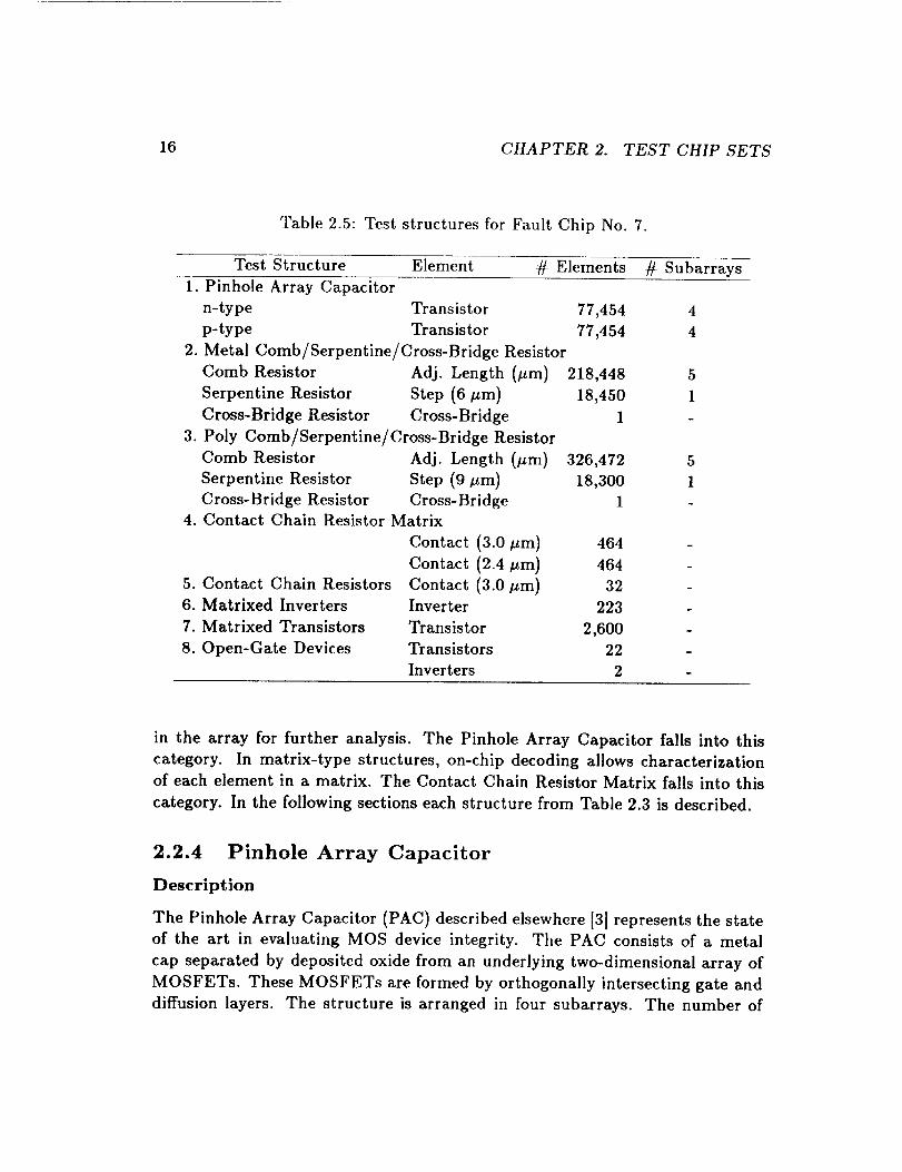
Table 2.5: Test structures for Fault Chip No. 7.
Test Structure Element # Elements # Subarrays
1. Pinhole Array Capacitor
n-type Transistor 77,454 4
p-type Transistor 77,454 4
2. Metal Comb/Serpentine/Cross-Bridge Resistor
Comb Resistor Adj. Length (#m) 218,448 5
Serpentine Resistor Step (6 #m) 18,450 1
Cross-Bridge Resistor Cross-Bridge 1 -
3. Poly Comb/Serpentine/Cross-Bridge Resistor
Comb Resistor Adj. Length (_tm) 326,472 5
Serpentine Resistor Step (9 #m) 18,300 1
Cross-Bridge Resistor Cross-Bridge 1 -4. Contact Chain Resistor Matrix
Contact (3.0 #m) 464
Contact (2.4 #m) 464
5. Contact Chain Resistors Contact (3.0 #m) 32
6. Matrixed Inverters Inverter 223
7. Matrixed Transistors Transistor 2,600
8. Open-Gate Devices Transistors 22 -
Inverters 2 -
in the array for further analysis. The Pinhole Array Capacitor falls into this
category. In matrix-type structures, on-chip decoding allows characterization
of each element in a matrix. The Contact Chain Resistor Matrix falls into this
category. In the following sections each structure from Table 2.3 is described.
2.2.4 Pinhole Array Capacitor
Description
The Pinhole Array Capacitor (PAC) described elsewhere [3] represents the state
of the art in evaluating MOS device integrity. The PAC consists of a metal
cap separated by deposited oxide from an underlying two-dimensional array of
MOSFETs. These MOSFETs are formed by orthogonally intersecting gate and
diffusion layers. The structure is arranged in four subarrays. The number of

2.2. FAULT TEST CHIP 17
elements in each subarray is listed in the Defect Location Map given in Fig-
ures 2.5 and 2.6. The PAC can be used to characterize gate and metal-poly
oxide defects. Metal-poly oxide defects are modeled by simple resistive shorts.
Experimental results show the range of these resistive shorts to be between 1
and 100 k_.
The origin of the gate oxide pinholes in a CMOS local oxidation process,
in which silicon nitride is used for gate oxide definition, is believed to be the
formation of residual nitride at the silicon surface which masks against gate
oxide growth [4,5,6] (Figure 2.3). This residual nitride results in a thinning
of the gate oxide at the affected regions, and allows the phosphorous from the
phosphorous-doped polycrystalline silicon gate material to dope the silicon n-
type.
NAKAJIMA KOrOI _
N,','R,o,=t _NH 3 _./_' 3 (
f f\ o×,,:,,=( --NITRIDE_ _
l SILICON
POLYCRYSTALLINE_ SIL_
THIN OXIDE_ OXIDE
SILICON
Figure 2.3: Gate Oxide defect origin, after Kooi (1976) and Nakajima (1979).
Analysis Technique
The first fault mechanism that is investigated is shorting between the metal cap
and the poly gate, IMP. A voltage is applied to the metal cap and the current
flow out the poly layer is measured.
The second fault mechanism investigated is shorting between the gate and
the source/drain region. To perform this measurement, shown in Figure 2.4, a
voltage is applied to various layers with the transistors either biased ON or OFF
and the current measured. Four different measurements are made: IPDON,
IPBON, IPDOFF, and IPBOFF. IPD is the current from Poly to Diffusion
and IPB is the current from Poly to Bulk. The ON suffix indicates that a channel
is present; OFF indicates that channel is absent. These four measurements allow
us to identify the particular gate oxide defect as shown in Table 2.6. Two types

18 CHAPTER 2. TEST CHIP SETS
STRUCTURE:n-PACDEFECT:CHANNEL:BULK:
TYPE # 1OHMICJUNCTION
_l- VG = _+5V
IPD T
( SILICON p
IPB _
STRUCTURE: I_PACDEFECT: TYPE _/2CHANNEL: JUNCTIONBULK: OHMIC
vG
IPD _-
/ - °
IPB
--_+SV
Figure 2.4: Two types of Pinhole Array Capacitor (PAC) structures where the
fault type is determined by the channel conduction type.
of PAC fault models are proposed to explain the four measured currents. The
type 1 defect models the n-PAC and the type 2 defect models the p-PAC. In the
first type, the pinhole forms an ohmic connection to the channel and a diode
connection to the bulk. In the second type, the pinhole forms a diode connection
to the channel and an ohmic connection to the bulk. From these models we have
prepared an expected response for the currents as shown in Table 2.7. This table
was prepared for both single and multiple faults. A multiple fault (e.g., BD)
is one in which two or more faults can lead to the same current path. If the
measured current is greater than or equal to I(CUTOFF) then it is assigned
the value "l"; otherwise, it is assigned the value "0". Initially I(CUTOFF) is
set to 1.0 x 10 -s A, but our software can modify I(CUTOFF) in the range of1.0 x 10 -9 to 1.0 X 10-_A to better fit the data. Each modeled defect has a
certain type of signature represented by four digits (see Table 2.7). From the
four measured currents, one can identify the nature of the defect. In some cases
other combinations of currents are observed. In these cases, the defect is not
modeled by the defects shown in Figure 2.4. When this occurs the defects usually
cover a large area and affect other adjacent subarrays. Notice in Table 2.7 that
the p-PAC is more diagnosable than the n-PAC. Thus, if you have to choose
between including a p-PAC or an n-PAC on a test chip, choose the p-PAC.

2.2. FAULT TEST CHIP 19
Table 2.6: Pinhole Array Capacitor defect classes.
Defect Classes
N No Defect Detected
B Poly-Bulk Defect
D Poly-Diffusion Defect
S Poly-Diffusion Defect (Side of Array)
M Metal-Poly Defect
P Probing Fault
? Other Defect
The PAC Data Analysis Program automates oxide defect categorization.
Detected faults are categorized in three steps. First, a gate-oxide four-current
histogram is generated, as seen in Figure 2.5. Letters of the alphabet are used
as symbols to represent PAC subarrays with defects. Second, a wafer map is
generated which shows the location of the faults on the wafer; see Figure 2.5.
This information is used to determine whether the fault is an isolated defect or
a cluster defect. Third, the defects are categorized as to the type of the defect.
Finally, a value for the elements per defect, E, is calculated for each category
and for all categories combined. Examples of this method for calculating these
values are shown in Figures 2.5 and 2.6.
The PAC Data Analysis program was used to analyze the results from two
3-#m CMOS/bulk PACs. The total number of elements for each PAC structure
is 70,434. Example results (both the raw data and the data analysis) are shown
in Figures 2.5 and 2.6. These show that p-PACs have a total of 6 isolated gate
oxide defects and one metal-poly oxide defect. Four of the gate oxide defects
are B, BD type and two are SB type. For example, the "a" defect, highlighted
in Figure 2.5, is clearly a B, BD type defect for its current exceeds I(CUTOFF)
in a 1101 sequence. The n-PACs have a total of one isolated gate oxide defect,
four P-P clusters, one other defect, and three isolated metal-poly oxide defects.
The gate oxide defect is type D, B, DB. The cluster defects are highlighted in
Figure 2.6 and in the Defect Location Map shown in Figure 2.6. When defects
are found in three or more adjacent subarrays, they are classified as a cluster
defect.
2O CHAPTER 2. TEST CHIP SETS
Table 2.7: Defect identification based on four Pinhole Array Capacitor tests.
IPDON IPBON IPDOFF IPBOFF TYPE 1 TYPE 2
n-PAC p-PAC
0 0 0 0 N N
1 0 0 1 B,D,DB D
1 0 1 1 S,SB,SD,SBD S,SD
1 1 0 1 ? B,BD
1 1 1 1 ? SB,SBD
ALL OTHER COMBINATIONS ? ?
NOTES: ON = Channel present
OFF = Channel absent
0 = Current less than I(CUTOFF)
1 = Current greater than or equal to I(CUTOFF)
2.2.5 Comb/Serpentine/Cross-Bridge Resistor
Description
The Comb/Serpentine/Cross-Bridge Resistor is used to characterize single layer
shorts and opens. This test structure consists of five combs, one serpentine, and
one cross-bridge resistor. The layout of the structure is shown in Figure 2.7.
Figure 2.8 shows a schematic representation of the Comb/Serpentine Resistor.
The Comb/Serpentine/Cross-Bridge resistor is available for Metal and Poly lay-
ers. Prior to measuring the structure, a probe down test is performed. Notice
that the probe pads for the structure shown in Figure 2.7 allow two probes to
touch each pad. The probe down test is passed when the two-terminal resistance
is less than some predetermined value which is usually 100 ohms.
The comb structures are used for detecting shorts between the serpentine
and the comb wires which are spaced according to the design rule limit. The
five combs have a different length adjacent to the serpentine. The serpentine
crosses over steps made by lower level layers. For example, the Metal serpentine
crosses over steps made by layers of poly and diffusion, and is used for detecting
breaks in the wire due to step coverage problems.
The cross-bridge resistor is used to locally measure the sheet resistance and
wire width where the bridge is formed over the highest level layer. This infor-
mation is needed to analyze the serpentine resistance measurements.

2.2. FAULT TEST CHIP 21
M44E WAFER 4 p-PAC
FAULT NUMBER OF OBSERVATIONS
CURR. IPDON IPBON IPDOFF IPBOFF IMP
1.0 × 10- i5 0 0 0 0 0
2.0 × 10 -15 0 0 0 0 0
5.0 x 10- 15 0 0 0 0 0
1.0 × 10 -14 0 0 0 0 0
2.0 × 10 -14 1 0 0 0 0
5.0 × 10- i4 0 2 1 0 01.0 × 10- i3 0 0 0 0 0
2.0 X 10⁻¹³ 8 2 3 a 1 0
5.0 × 10-t3 7 3 4 0 0
1.0 x 10 -12 12 12 17 0 1
2.0 × 10⁻¹² 8 22 19 d 24 10
5.0 × 10- i2 6 1 1 e 9 12
1.0 x 10 -ii 0 0 0 6 7
2.0 x 10 -_l 0 0 0 2 13
5.0 x 10 -li 0 0 0 0 2
1.0 × 10- lo 0 0 0 0 2
2.0 x 10- lo 0 0 0 0 0
5.0 × 10- 1. 0 0 0 0 0
1.0 x 10 -9 0 0 0 0 02.0 x 10 -9 0 0 1 f 0 0
5.0 x 10 -° 0 0 0 0 0
I(CUTOFF)1.0 x I0 -s 1 d 0 0 0 0
2.0 x 10 -s 0 0 0 0 0
5.0 x 10 -s 1 a 0 0 0 0
1.0 × 10 -7 0 0 0 0 0
2.0 × 10- r 0 0 1 b 0 0
5.0 X 10 -7 0 0 0 0 01.0 × 10 -c 0 0 1 c 0 0
2.0 × 10 -G 3 bef 0 0 0 0
5.0 × 10 -G 1 c 0 0 0 0
1.0 x I0 -s 0 0 0 0 0
2.0 x 10 -s 0 0 0 0 0
5.0 x 10 -5 0 1 b 0 1 b 0
1.0 x 10 -4 0 0 0 1 c 0
2.0 × 10 -4 0 4 acef 0 3 aef 0
5.0x 10⁻⁴ 0 1 d 0 1 d 1
1.0 x 10 -3 0 0 0 0 02.0 x 10 -3 0 0 0 0 0
5.0 x 10 -3 0 0 0 0 0
INC/EXC 48/0 48/_0 ..... 4_8/0 .... 48/0_ ..... 48_/0cUTOi_F < 1()-g Amps STRESS VOLTAGE = 5.0 VLOWER BOUND SHOWN FOR HISTOGRAM INCREMENT
C,URRENT SOURCE BOUND APPROX = 20 mA
Figure 2.5: P-PAC test results for run M44E, wafer 4.

22 CHAPTER 2. TEST CHIP SETS
DEFECT LOCATION MAP:
M44E WAFER 4 p-PAC
N/PP
P/PD
COL 1144488ACCDD
ROW 582585825858
2709 ............
8127 ............
18963 .......... N-
40635 ............
2709 ............
8127 ...... a .....
18963 .... b-c---d-
40635 --e---f .....p-PAC DEFECT ANALYSIS
GATE OXIDE DEFECTS
TYPE CLUSTERS OTHER TOTAL
D S B,BD SB P-P M-P ELEMENTS
70434FAULT
SITE
Z (×1oES (×.1o 4)
e b
a c
f
d
> 3.6 > 3.6 2.1 6.0
*** *** 2.6 66
> 3.6 > 3.6 > 3.6 1.5
4.8
NO. OF
FAULTS
E (xl0 _)
ES (xl04)
METAL-POLY FIELD OXIDE DEFECTS
CLUSTERS OTHER TOTAL
M-M M-P ELEMENTS
i 0 0 0 70434
13 > 3.6 > 3.6 > 3.6 13
1.4 *** *** *** 1.4
Figure 2.5: P-PAC test results for run M44E, wafer 4 (Continued).

2.2. FAULT TEST CHIP
M?4E WAFER 4 n PACFAULT .... r -
CURR. NUMBER OF OBSERVATIONS1.0×10-,, /PDON _/PBON
• - IPDOFF IPBOFF I2.0 ,< 10-1`5 MP
0 0 0 0
0 I 05.0 × 10- _5 0 I 0 0 01.0 × 10⁻¹⁴ 0 0 0 02.0 x 10⁻¹⁴ 0 1 1 05.0 × i0-14 0 0 0
01 0 0
1,0 X 10 -13 0 2 2 1 02.0 × 10- z3 0 4 2 15.0 × 10-_3 6 9 7 11.0 × 10⁻¹² I0 9 1
22,0 × 10⁻¹² 19 9 6 6 35.0 × I0-12 5 19 201.0 × 10- lj 4 3 13
2 150 0 0 8 5
2.0 × lO-ll 1 1 d 0 15.0 x 10-J_ 0 0 0 31.0 × I0- lo 0 I 0
20 0 0
2.0× I0-1° 0 I 2 bd 0 05.Ox 10-_o 3 abe 0 3 ace 01.0 × 10-o I e 0 0 0
2.0 × I0-O 0 0 0
5,0 >_ 10-9 0 0 0 0 O
2.0 x lO-S 0 I e 05.0 × lO-S 0 0 0
1.0 x I0-r 0 0 0 0 0
0 0 02.0 × lO--r 0 0 0 0
5.0 × 10⁻⁷ 0 0 0
1.0 × 10-o 0 0 0 0 0
2.0 × 10⁻⁶ 0 0 0 0 00
0 1 f 05.0 x I0-6 0 1 f 0 0 0
1,0 × 10-,5 0 0 0 0 0
2.0 x 10⁻⁵ I d 0 0 0 05.0 × 10-_ 0 0 0 01.0 x 10⁻⁴ 0 0 0 02.0 × 10⁻⁴ 1 f 0 I d
5.0 × 10⁻⁴ 0 0 I f 0 0
1.0 × jO-a 0 0 0 0 02
2.0 x I0-_ 0 0 0 0 15.0 x 10-a 0 0 0
v _xftE, SS VOL-'PA_s---_- ........ az/1LOWER BOUND SHOWN FOR "'-"-,_ = 5.0 V ...............
HISTOGRAM INCREMENTCURRENT SOURCE BOUND APPRox = 20mA
Figure 2.6: N-PAC test results for run M44E, wafer 4.
23

24 CHAPTER 2. TEST CHIP SETS
DEFECT LOCATION MAP:
M44E WAFER 4 n-PAC
N/NP
P/ND
COL II44488ACCDD
ROW 582585825858
2709 ........ P---
8127 --M .........
18963 ............
40635 -M ...... N---
2709 a ....... P---
8127 b ...........
18963 c ..... d .....
40635 e .......... f
n-PAC DEFECT ANALYSIS
FAULT
SITE
E (xl0 5)
ES ( x lO4)
l TYPED,B,DB S,SB
d
13 > 3.6
140 ***
GATE OXIDE DEFECTS
CLUSTERSP-P M-P
a
b
C
e
3.4 > 3.6
14 ***
OTHER
5.9
15
TOTALELEMENTS
70434
1.8
4.1
NO. OF
FAULTS
ES ( × 10 4)
METAL-POLY FIELD OXIDE DEFECTS
TYPE CLUSTERS OTHER TOTAL
M M-M M-P ELEMENTS
3 0 0 0 70434
_:6 > 3.6 > 3.6..... _.6 ....... _._ -6.9 *** *** *** 6.9
Figure 2.6: N-PAC test results for run M44E, wafer 4 (Continued).

2.2. FAULT TEST CHIP 25
Analysis Technique
The serpentine resistance, Rserp, is measured by forcing a current through the
serpentine and measuring the voltage drop. The serpentine effective length,
Lserp, is
R_erp × Wb_idg_,highLserp ----
Rs,bridge
where Wbridge,high is the width and Rs,bridg_ is the sheet resistance. L,e_p is com-
pared with the as-drawn serpentine length. If the effective length is longer than
150% of the as-drawn length then the serpentine is considered to have a step-
coverage problem and the site is flagged as faulty. The apparent serpentine
length is due to a combination of one or more of the following:
1. Serpentine wire thinning and necking at the step.
2. Undulation due to the serpentine wire crossing over steps.
3. Width of high lying layers being different from low lying layers.
4. Under/over sizing of the underlying features due to over/under etching.
Wire shorts are detected by suppling 5 V between the serpentine and the comb
wires. If the _eakage current between two layers is greater than 10.0 nA, the
wires are considered shorted and the site is flagged as faulty.
A software program has been developed to analyze the raw data gathered
from the Comb/Serpentine/Cross-Bridge resistor. The program generates a
histogram of the effective length of the serpentine wires and calculates the defect
densities for the wire shorts and opens detected.
The analysis results for Poly Comb/Serpentine/Cross-Bridge resistor for run
M61P are shown in Figure 2.9. No short or open defects in the poly comb were
observed for the M61P run. Notice that Lserp -_ 169931 _m which is 3.2 percent
larger than Las.draw n : 164700#m. The "P" shown for the serpentine indicates
that a probing fault was encountered.
2.2.6 Contact Chain and Contact Chain Matrix
Description
The Contact Chain Structure [7] consists of eight contacts connected to form a
chain. Since these contacts share the same current path they consume less silicon
area than individual contacts. Figure 2.10 shows the layout of the Contact Chain
Structure. The four types of Contact Chain Structures are:

ORIGINAL PAGE IS
OF POOR QUALITY
26 CHAPTER 2. TEST CHIP SETS
CROSS-BRIDGE
Figure 2.7: The Comb/Serpentine/Cross-Bridge Resistor in First-Layer Metal
with poly crossovers.

2.2. FAULT TEST CHIP
i
SERP. COMBIN 1
--_1!i
I
i
I m
! '
E-]COMB
3
E.• E-!COMB COMB SERP. COMB
2 4 OUT 5
27
Figure 2.8: Schematic diagram of the Comb/Serpentine Resistor which is seg-
mented into five subarrays.
1. p+Poly/Metal,
2. n+Poly/Metal,
3. p+Diff/Metal, and
4. n+Diff/Metal.
However, the Contact Chain Structure does not provide enough data on
each chip to enable a meaningful contact probability analysis. Thus, the Con-
tact Chain Matrix Structure was designed and included on Fault Chip No. 7.
Figures 2.11 and 2.12 show the Contact Chain Matrix layout schematic and
the Contact Chain Matrix transistor level schematic, respectively. The Contact
Chain Matrix Structure included on Fault Chip No. 7 consists of four different

28 CHAPTER 2. TEST CHIP SETS
Identity of failed chip - by location in chip carrier
M61P CHIP
NO.
COMB 16056
29436
50844
66900
163236
SERP. 183OO
11111111112222222222
123456789A123456789A
........ p ...........
SERPENTINE LENGTH HISTOGRAM
0
166943 0
167690 3 ***
168437 3 ***
169184 5 *****
169931 2 **
170678 4 ****
171425 0
172172 1 *
172919 1 *
+ 0
As-Drawn Serpentine Length = 164700 (#m) - -
Open Serpentine Wires = [0], High Res. Serpentine Wires = [0]
Shorted Combs = [0]
nserp (#m) Avg/StDev/Inc/Exc/Inv = 169931/1.39 × 103/19/0/1
Rserp (12) Avg/StDev/Inc/Exc/Inv = 812856/3.30 x 104/19/0/1
Rs,bridg e (fl) Avg/StDev/Inc/Exc/Inv = 14.5/1.11/20/0/0
Wbridge,hig h (>m) Avg/StDev/Inc/Exc/Inv = 3.03/0.228/20/0/0
YIELD ANALYSIS (Total # Sites = 20) ........
Shorts Opens
Total # Elements 6529440 (_m) 366000 (Step: 9/_m)
Total # Shorts 0 (#m) NA
Total # Defects NA 0
Elements/Defect > 2.13 × l06 (_m/Defect) > 3.66 × 10⁵ (Steps/Defect)
Std. Deviation ******* *******
Figure 2.9: Test results of Poly Comb/Serpentine/Cross-Bridge on M61P run.

2.2. FAULT TEST CHIP 29
POLY AND
METAL
DIFFUSION
VII Vl2
r
AFteRt_ENEWEG(19S6_
Figure 2.10: Contact Chain Structure.
types of contacts: p+ and n+Poly/metal and p+ and n+Diff/Metal. There
are 116 contacts for each contact type. The Contact Chain Matrix Structure
consists of 8 rows and 58 columns. The contacts in each row of the matrix share
the same current path to save silicon area.
The Contact Chain Matrix Structure, by using one randomly accessible ma-
trix, replaces the four contact matrix structures which were needed to access the
different types of contacts. This saves area which would otherwise have been
consumed by the necessary overhead circuitry and pads.
An early version of the Contact Chain Matrix Structure included 2nd metal
to 1st metal via resistance chains. This structure was unsuccessful because
excessively large currents were required to generate measurable voltages.

30 CHAPTER 2. TEST CHIP SETS
58 CONTACTS
METAL TO N-DIFFMETAL TO P-DIFFMETAL TO P-DIFFMETAL TO N-POLYMETAL TO N-POLYMETAL TO P-POLY
58 CONTACTS58 CONTACTS •58 CONTACTS •58 CONTACTS •58 CONTACTS •58 CONTACTS •
V21
Vll
V22
V12
12
V21 V22
Vll V12
12
_m
I_ DIFFUSION _ POLY l'-'1 METAL
Figure 2.11: Contact Chain Matrix with 464 contacts. Developed to characterize
the four types of contacts found in a single-metal 3-#m CMOS process.

2.2. FAULT TEST CHIP 31
---x.__.4
cc I
"'- _ I
R4-RO O_
r--
...
l ] ...
- COL
-I_o w
- COL
IROW
-FRO w
ROW
-1 COLDECODER C_5-C I_=CONTACTCELL0
Figure 2.12: The Contact Chain Matrix, where the row and column addressing
circuitry allows the measurement of each contact denoted by an X.
Analysis Technique
The test procedure calls for forcing a current of known value (64#A/#m 2)
through the Contact Chain and measuring the voltage drop over the contact
surface. This is a four-terminal measurement and allows accurate measurements
of the contact interfacial resistance.
The contacts are characterized by three numbers: the mean, the standard
deviation, and the probability of encountering an open contact, based on contact
probability analysis [7]. This technique, shown in Figure 2.13, assumes a normaldistribution of contact conductance. The cumulative distribution of contact
conductance is plotted on the "probability scale and a line is fitted using a Chi-
square linear fit. The intersection of the fitted line and the probability axis is
taken to represent the probability of a contact having zero conductance, i.e.,
the probability of an open contact. This provides a characteristic number which
can be used to assess the difference between processes, and/or vendors. The

32
{gJ
o<[b-zO¢Jit
NORMAL DISTRIBUTION
Gp-Go Gp Gp+Ge G
CHAPTER 2. TEST CHIP SETS
CUMU LATIVE DISTR IBUTION(LINEAR SCALE)
10o%I
0% 3
G/x-Go Gp G/J+Go G
PROBABILITY Gi < G
.... PROBABILITY Gi > G
A
L_>.I---I
<_
O
O.
90%
50%
10%
CUMULATIVE DISTRIBUTION(PROBABI LITY SCALE)
B
Gp-Go Gp Gp+Go G_
CUMULATIVE DISTRIBUTION
(GRAPH ROTATED)
fG
G/J+ Go
Gp
Gp - Gcr
1
10% 50% 90%
PROBABILITY Gi > G
I99%
Figure 2.13: Contact resistance probability analysis method.
characteristic number depends on the ratio between the population mean and
the population standard deviation. Figure 2.14 Shows the contact probability
analysis for 3.0-#m p+Poly/Metal contacts of run M62Z. The probability of
encountering an open contact for the p+Poly/Metal contacts of run M62Z is1.947 x 10 -7 .
2.2.7 Floating Gate Transistors
Description
The floating gate transistor is a transistor with an isolated poly gate wire. The
behavior of the transistor is expected to depend on the initial charge induced on
the gate by the process and the charge induced from the measurement potentials.
The floating gate transistor models for n- and p-channel transistors are shown
in Figure 2.15. The three capacitances involved in determining the behavior of
the floating gate transistors are the gate-to-drain capacitance, Cgd, the gate-to-

2.2. FAULT TEST CHIP 33
15:35:11 22-MAY-86RK 1 :M62ZCT. 103 CREATED: 17:16:08 16-APR-86 BY CRUNCH VERSION 6
RUN M62Z (FAULT CHIP5) P + POLY CONTACT CHAIN STRUCTURECONTACT CUT WIDTH = 3.0 UM; STRESS CURRENT = 64 i_A/p.m2
(CP3CTP + POLY 3.0)LAYER = P + POLY SIZE = 3.0 um
zuJ:SI.U
800
70O
600
5OO
4OO
300 -
200 -
100 -
0
E-3
I
[] []
• %
-- _ _ ° ° °°_/.e
q
I I I I
Iii
J
I 1.3 .5 .7
I I I I.01 .1 .9 .99 4N 5N 6N 7N 8N
PROBABILITY P(GI > G)
Q,•
eBqk, OQ
1 i i *b,.I
3N
#PROBE ERRORS= 0# OPEN CONTACTS = 0
# CONTACTS INCLUDED/EXCLUDED = 144/0PROBABILITY OF AN OPEN CONTACT = 1.947E-07
ERROR = 9.068E-09
Figure 2.14: Contact Probability Analysis for p+Poly/Metal contacts of run
M62Z. The analysis technique was developed at JPL by U. Lieneweg and D. Han-
naman.

34 CHAPTER 2. TEST CHIP SETS
D
S
GC
Cgd
-t' I
Cgbo
CgsI-4,
f
S
cl = Cgd
i Cgbo + Cgs
C2_ B
G
Cgs
Ggbo
Cgd
D
B
C1 = Cgbo + Cgs
C2 = Cgd
n - CHANNEL FLOATING GATE MODEL p- CHANNEL FLOATING GATE MODEL
Figure 2.15: Floating gate transistor models where the body is shorted to the
source.
source capacitance, Cgs, and the gate-to-bulk overlap capacitance, Cgbo. Cgbo
depends on the area of the poly over the field oxide.
Analysis Technique
The test setup for testing floating gate transistors is shown in Figure 2.16. A
voltage is applied to the drain of the transistor and the resulting current through
the source is measured. In run M56G the floating gate transistors with a gate
length of 3/_m and a gate overlap length of 26 #m were tested with a drain-to-
source voltage of 5 V. The floating gate p-channel transistors were "ON" with a
channel current of about 1.0 × 10 -6 A, and the floating gate n-channel transistors
were "OFF." The floating gate transistor voltage is the gate voltage required
to cause the same current to flow in a calibrator transistor. The calibrator

2.2. FAULT TEST CHIP 35
FLOAT I _O
S
()7
n-CHANNEL
+--SV FLOAT I
p-CHANNEL
Figure 2.16: Test setup for floating gate transistors.
+m m+5 V
\7
transistor is fully connected and provides transistor I-V curves. The floating gate
device analysis using a calibrator transistor is shown in Figure 2.17. Transistor
I-V curves from the calibrator transistor are used to estimate the floating gate
voltage for a given drain-to-source voltage and channel current. It is estimated
that for run M56G the gate voltage of the n-channel transistors is less than VTn,
and the p-channel transistor Vgd = 3.5 V (Vgs = -1.5 V). The gate voltage of
the floating gate transistors is calculated from the following equation, using the
capacitor-divider models shown in Figure 2.15
(JVDS I - YGi) × (1-e -qRc)VG = VG, +
1 + C2/CI
where C = C1 × C2/(CI + C2), C1 = Cgd and C2 = Cgbo+ Cgs for n-channel
transistors (C1 -- Cgbo+Cgs and C2 = Cgdfor p-channel transistors), and VGi
is the process-induced charge on the gate. Also R is the resistance in series with
the external voltage source. The time constant, RC, is of the order 1.0 × 10 -l_
seconds. Thus for time t >> RC this equation becomes
(I VDSI - VGi)VG = VGi +
,+ c2/cl
Since the gate delay of the CMOS devices is much larger than the time con-
stant RC, the transition time between the initial state and the steady state is
negligible. The initial gate voltage, VGi, represents the gate-to-source voltage
36 CHAPTER 2. TEST CHIP SETS
CALIBRATOR TRANSISTOR TRANSISTOR UNDER TEST
VG I
_VD _ VD=._ FLOAT
, I' I
- ,oC) ,o()
LOG ID vo3-_ LoGJDI_°_ _-_- - -I - -x 25r,- ,VDI__ .....
J/i i _--/_ ! !I/I I I
VG1 VG2 VG3 VG _ VD1 VD2 VD3 VD ---_
VG3
VG2
VG1
VG i , I IVD1 VD2 VD3
Figure 2.17: Floating-Gate device analysis.

2.2. FAULT TEST CHIP 37
at a drain-to-source voltage of zero volts, and is important for simulating the
behavior of the floating gate transistors.
The initial gate voltage can be determined from experimental measurements
when VGi << VDS, as shown in Figure 2.17. When VGi << VDS the above
equation becomes
IVDSJVG = VGi +
1 + C2/C1
A minimum of two floating gate voltage measurements at different drain-to-
source voltages are required to estimate the initial gate voltage. In Figure 2.18
we observe that the estimated initial gate voltage for run M61P is 0.18 V and that
the gate voltage for n-channel floating gate transistors is inversely proportional
VG i=0.18 0.--_
0
RUN _161P CHIP -_,1
L = 12p.m
L= 21/am
L = 33/am
L= 63#m
I I I I I=1.0 2.0 3.0 4.0 5.0
VDS (VOLTS)
Figure 2.18: Floating gate n-channel transistor analysis of run M61P. The L is
the gate poly overlap length of the floating gate transistor. The channel width
and length are 4.5 and 3.0 #m, respectively.

38 CHAPTER 2. TEST CHIP SETS
to the gate poly length. We also observe that the gate voltage for p-channel
floating gate transistors is directly proportional to the gate poly overlap length.
As the gate poly overlap length increases, both the n- and p-channel floating
gate transistors operate closer to their "OFF" state. Figure 2.19 shows the
experimental results of the gate poly overlap length variations on the conduction
state of the n-channel transistor. As expected, the results in Figure 2.19 correlate
with the theoretical results.
In order to study the behavior of floating gate transistors in an inverter,
we have designed faulted inverter structures. The two types of faulted inverter
structures are shown in Figure 2.20. The first structure has individual floating
gate poly wires for the n-channel and the p-channel transistors. The second
structure has a common floating gate poly wire for the n-channel and p-channel
transistors. The above equations are valid for calculating the gate voltage of the
n- and p-channel floating gate transistors of the first faulted inverter structure.
The common gate voltage of the second faulted inverter structure is calculated
using( VDD - vai)(1 - e-,/RO)
VG = VGi +1 + C2/C1
where C = (C1 x C2)/(C1 + C2), C1 = Cgs2 + Cgbo2, C2 = Cgsl + Cgbol,
and Cgd2 and Cgdl are ignored.
At time t >> RC (RC is in the order of 1.0 × 10 -13 seconds), we have
(VDD-VCi)VG = VGi +
1 + C2/C1
Since we can assume that C1 = C2 and VGi << VDD, we expect a gate voltage
of VDD/2 for the second faulted inverter structure.
The analysis of the faulted inverter structures of the M56G run shows that
the first type of faulted inverters is stuck high with an output voltage of between
4.0 and 5.0 V. This observation is consistent with the results for individual
floating gate transistors: the p-channel floating gate transistor is "ON" and
the n-channel floating gate transistor is "OFF" for a gate poly overlap length
of about 26 #m. The second type of faulted inverters draws almost maximum
current and the output voltage is at about 2.5 V or VDD/2. This observation
implies that for this configuration the p-channel and the n-channel transistors
are "ON" with the gate voltage of about 2.5 V which confirms our assumptions.
The work on the floating gate transistors is still under way; many observa-
tions have not yet been fully analyzed or understood. Better test structures
have been developed and are expected to be functional on future Fault Chips.

2.2. FAULT TEST CHIP
10-5 I
a.,5:
I'-Zu,,I
CC
(3
UL,I
C_
0O9
0I-"
ZN
10-6
10-7
10-8
10-9
10-10
0
#1 A
' I ' I ' 1 I 1 ; I '1 #2o
39
#11
w
Us
#18
0
Figure 2.19:
on the conduction state of the n-channel transistor for VDS -= 5 V.
analysis for this device is shown in Figure 2.18.
I I J I , 1 , I = i _ I ,10 20 30 40 50 60 70
FLOATING GATE POLY OVERLAP LENGTH (/mr)
Experimental results of the gate poly overlap length variations
The VGi

4O CHAPTER 2. TEST CHIP SETS
Cgs2
r--t5V 5 5V
FLOAT
//
FLOAT
II
Cgd2OUT
O
FLOAT
Cgbo2
Cgd2
Cgbol
Cgsl
OUT
TYPE 1: ISOLATED p- AND n-CHANNEL
TRANSISTOR GATESTYPE 2: CONNECTED p- AND n-CHANNEL
TRANSISTOR GATES
Figure 2.20: Two types of the faulted inverter structure.
2.2.8 Matrixed Inverters
The inverter matrix test structure consists of 225 randomly accessible inverters
and is used for inverter parameter variability analysis [8]. This structure can
also be used for inverter defect characterization. The parameters measured by
this structure are: Inverter Threshold Voltage (Vinv), Inverter GAIN, Vhigh,
Vlow, and Noise Margin, Vnm = (l - 1/GAIN) × Vinv.
2.2.9 Matrixed Transistors
The initial Transistor Matrix test structure consists of 2600 randomly accessible
n-channel transistors. A p-channel pull-up transistor is associated with each
row of the matrix and can be used as a pull-up transistor to form an inverter

2.2. FAULT TEST CHIP 41
with the n-channel transistors. The transistor matrix is used for parameter
variability analysis and for characterization of process faults and their effects
on transistor parameters. The transistor parameter measurements are time
consuming; therefore, the transistors are combined with the pull-up devices to
form inverters. The inverter threshold measurement is fast and is used as an
initial test. When problems are detected in this preliminary test, more extensive
tests can follow.
The initial transistor matrix is somewhat limited in that only d.c. parameters
can be tested and analyzed: gate oxide pinholes, for example, are not expected to
show up in the d.c. parameters. To locate these defects the transient transistor
behavior must be monitored and timing analysis must be performed. Also, a
complete oxide Pinhole Test is needed to characterize any oxide defects detected.
A new transistor matrix was designed to overcome these limitations. Fig-
ure 2.21 shows the circuit schematic of this test structure and its five modes of
operation. These operational modes make it possible to perform all transistor
and inverter matrix functions. The five modes of operation of the new transistor
matrix structure are as follows:
1. Gate oxide integrity: A quick test to detect whether any oxide defects
exist.
2. Transistor d.c. parameter extraction: Parameter variability analysis.
3. Transistor transient behavior: Timing analysis to locate slow transistors.
4. Gate pinhole characterization: A complete Pinhole Array Capacitor test.
5. Inverter threshold: Parameter variability analysis.
This structure is under development and will be analyzed as time permits.
2.2.10 Fault Chip Summary Results
The Fault Chip is being fabricated on a periodic basis by MOSIS. Three sum-
mary reports are included in this section. The first summary was produced
for run M61P on Fault Chip No. 3. The M61P summary results are shown in
Table 2.8. The Pinhole Array Capacitor and Contact structures were not in-
cluded in this report because design problems made these structures untestable.
The major problem observed is a metal step coverage problem: eleven of twenty
metal serpentine wires were open. (Figure 2.22 shows SEM photos of top view
and cross section of broken metal serpentine wire of the M61P run.) The metal

42 CHAPTER 2. TEST CHIP SETS
Table 2.8: FAULT CHIP ANALYSIS FOR 3-#m CMOS/BULK
Prepared by H. Sayah(hrs), Reviewed by: M. Buehler(mgb), C. Pifia(cap)Date: 4-15-86. Revised 4-21-86.
Report No. 1. Run No. M61P. Fault Chip No. 3
Note: Fault Chip was fabricated twice on each of l0 wafers.
TABLE 1. SUBARRAY DEFECT ANALYSIS
Defect Type E-value Std.
_ . Elements/Defect Dev:
a} Comb Resistor: (Shorts}
Metal-Metal > 1.5 x i0 _; - 0/20
Poly-Poly > 2.1 × l0 G - 0/20
b) Serpentine Resistor: (Opens}
Metal Wire 2.3x 10⁴ -
Poly Wire > 3.7x 10⁵ - 0/20
Sites Total Element
Bad/Total Elements
4368960 length(l#m)
6529440 length(l#m)
369000 steps(6 #m)
366000 steps(9 #m)
TABLE 2. PARAMETER VARIABILITY ANALYSIS
Parameter (Dimensions) Average Std. Points
Value dev. Incl/Excl
o.32 2o/o3.03 o.23 2o/o
33. 3. 20/0
14.6 1.1 20/0
a) Cross-Bridge Resistor:
Metal Linewiclth (#m)(4.5 #m)
Poly Linewidth (#m)(3.0 #m)
Metal Sheet Resistance(roll/[] )
Poly Sheet Resistance(l-l/[] )
b) Transistor/Inverter Matrix:
(2500 Transistors/Chip)
Chip# l:Inverter VT(V)
Chip# 2:Inverter VT(V)
c) Floating Gate n-channel Transistors:
(W/L : 6.0 .m/3.0 #m)
Initial Gate Voltage (V)
2.44 0.08 20/0
2.45 0.07 19/0
0.18 4/0

2.2. FAULT TEST CHIP 43
TEST #0: GATE INTEGRITY
TEST _' 1 : TRANSISTOR DC PARAMETER EXTRACTION
TEST # 2: TRANSISTOR TRANSIENT BEHAVIOR
TEST//3: GATE PINHOLE CHARACTERIZATION
TEST #4: INVERTER THRESHOLD
• : ,* .. ::• • • • Do
VD FORCE
VDF/I MEAS
GND
I MEASURE
SENSE
ENABLE
HIGH
LOW
HIGH
HIGH
PULL UP OUTPUT
HIGH FLOAT
STEP UP SENSE
HIGH FLOAT
NODEA FLOAT
VG FORCE
FORCE
PULSE
FORCE
NODE A
-I-
VDDSUBSTRATE I I GNDWELL [
Figure 2.21: Transistor Matrix test circuit.
VD SENSE
SENSE
GNO
I MEASURE
NODE A
IMEASUREGNDGNDIMEASURE
GND
linewidths are undersized. As reported in Table 2.8 the nominal linewidth is 4.5
#m; whereas the measured linewidth is 3.06 #m. This may have contributed to
the problem. No other defects were observed on this run and all other parametric
results are normal.
The second summary report was produced for run M62Z on Fault Chip No.
5. The M62Z summary results are shown in Table 2.9. Gate oxide defects are
prominent in this run: Nine out of eighteen sites have p-type gate oxide de-
fects and two out of eighteen sites have n-type gate oxide defects. The effect of
these defects on transistor performance has not yet been precisely determined.
However, simulation lends evidence that these defects degrade the timing per-
formance of active elements. The extent of such degradation depends on the
defect resistance, type, and associated circuitry. The other notable information

44 CHAPTER 2. TEST CHIP SETS
NITRIDE LAYER
SiO2 LAYER
METAL LAYER
SiO 2 LAYERPOLY LAYER
BROKEN STEP
a) CROSS-SECTION SEM PHOTO
}METAL LAYER
POLY LAYER
BROKEN STEP
b) TOP VIEW SEM PHOTO
Figure 2.22: Cross section and top view SEM photos of the broken metal ser-
pentine wire of run M61P.

2.2. FAULT TEST CHIP 45
Table 2.9: FAbLT CHIP ANALYSIS FOR 3-#m CMOS/BULK
Prepared by H. Sayah(hrs), Reviewed by: M. Buehler(mgb), C. Pifia(cap)
Report No. 2. Run No. M62Z. Fault Chip No. 5. Date: 5-28-86
Note: Fault Chip was fabricated twice on each of 9 wafers.
TABLE 1. SUBARRAY DEFECT ANALYSIS...................................
Defect Type E-value Std. Sites Total
Elements/Defect Dev. Bad/Total Elements
Element
a) Comb Resistor (Shorts):
Metal-Metal :> 1.3x 10 _
Poly-Poly > 1.9× l0 G
b) Serpentine Resistor (Opens):
Metal Wire > 3.3x10⁵
Poly Wire > 3.2)<105
c) p-Pinhole Array Cap.:
Metal-Poly Shorts 2.5 x 10 _
Gate Ox. Defects 9.1x10⁵
d) n-Pinhole Array Cap.:
Metal-Poly Shorts > 6.8×10⁵
Gate Ox. Defects 1.2x10⁵
2.7xi0 6
5.3x10 _
1.3xlO 4
0/18 3932064 hngth(1 #m)
0/18 5876496 length{ 1 pro)
0/18 332100 steps(6pm)
0/18 329400 steps(9pm)
1/18 1630944 capacitor
1630944 transistor
0/18 1630944 capacitor
_ 9/18[ 1630944 transistor
TABLE 2. PARAMETER VARIABILITY ANALYSIS
Parameter (Dimensions) Avg. Std. Prob. of Points
Value Dev. Open Incl/Excl
a) Cross-Bridge Resistor:
Metal Linewidth(#m) (4.5#m)
Poly Linewidth (#m)(3.0#m) 2.94
Metal Sheet Res. (rnfl/[:]) 30.
Poly Sheet Res. (n/El) 14.1
b) Contact Array Resistor (Contact size: 3.0 #m)
p+Poly/Metal (I])
n+Poly/MetM (fl)
p+Diff/Metal (fl)
n+Diff/Metal (fl)
0.o8 18/00.13 18/o1. 18/0
0.59 18/0
1.95×10⁷ 144/0
5.42x10⁷ 144/0
1.53x10 c 144/0
1.15x10 s 144/0

46 CHAPTER 2. TEST CHIP SETS
for this run is the undersized metal linewidth. The nominal wire width is 4.5
#m; the measured linewidth was 2.67 #m. However, no metal step coverage
problems were observed due to the undersized metal wire.
The third summary was produced for run M63E on Fault Chip No. 5. The
M63E summary results are shown in Table 2.10. From the summary report it
is seen that twelve of twenty-eight sites have p-type gate oxide defects and four
out of twenty-eight sites have n-type gate oxide defects. As explained previously,
this type of defect could degrade the timing performance of circuits fabricated
during this run.
Another observation relates to defective Diffusion/Metal contacts. The prob-
ability of occurrence of an open contact is significantly higher than in previous
runs. Further, the metal linewidths are again undersized. The nominal is 4.5/zm
and the measured was 2.81 #m. No metal step coverage problems were observed
as a result of metal linewidth undersizing.
2.2.11 Fault Prioritization Process
It is of major significance that the defect densities generated in the Fault Chip
summary reports can be used to prioritize likelihood of faults for a specified cir-
cuit based on layout geometry. Since the geometry and the number of basic cell
elements are not the same for different circuits, the responses of these circuits to
the process defects are different. For example, a circuit with no adjacent poly
to poly layers will not experience any poly to poiy layer shorts, no matter how
bad the process control. Therefore, the priority of poly to poly shorts for this
circuit is zero. Prioritization of faults is needed for proper design, simulation,
and testing of integrated circuits. Figure 2.23 shows the process of fault pri-
oritization. In Figure 2.23 Ei represents the estimated Elements/Defect from
the Fault Chip for the ith-type defect, Ni represents the number of the ith-type
elements in the specified circuit, and Di = Ni/Ei is the fault priority for the
ith-type defect.
For the example circuit specified in Table 2.11, we have prepared a fault
priority listing, shown in Table 2.12, based on the results of the Fault Chipsfrom the MOSIS run No. M62Z discussed in Table 2.9. The results in Table 2.12
were scaled using Di = 104Ni/Ei. As seen in Table 2.12 the n-type gate oxide
defects have the highest priority and are expected to be the major cause of
problems for the example circuit.

2.2. FAULT TEST CHIP 47
Table 2.10: FAULT CHIP ANALYSIS FOR 3-_m CMOS/BULK
Prepared by: H. Sayah(hrs), Reviewed by: M. nuehler(mgb), C. Pifia(cap)
Report No. 3. Run No. M63E. Fault Chip No. 5 Date: 7-30-86
Note: Fault Chip was fabricated twice on each of 14 wafers.
TABLE 1. DEFECT ANALYSIS
Defect Type E-value Std.
.......... Element_s/De.fect De v.
a) Comb Resistor (Shorts}:
Metal-Metal > 2.0x l0 G
Poly- Poly 5.3 x 10⁶
b) Serpentine Resistor (Opens):Metal Wire 7.7 x 10⁴
Poly Wire > 5.1x 10⁵
c) p-Pinhole Array Cap.:
Metal-PolyShorts > 1.1×10 G
Gate Ox. Defects 5.1x10⁵
d) n-Pinhole Array Cap.:
Metal-Poly Shorts 1.8× 10⁶
Gate Ox. Defects 1.3x10⁵
Sites Total Element
Bad/Total Elements
0/28 6116544 length(_m)
2.9>(10 ¢ 2/28 9141216 length(_m)
6/28 516600 steps(6Dm)
0/28 512400 steps(9Aum )
0/28 2537024 capacitor
5,9x 10' l -4/28 ] 2537024 transistor
4.6 x 10⁵ 1/28 2537024 capacitor
7.7×I03112/28 I 2537024 transistor
TABLE 2. PARAMETER VARIABILITY ANALYSIS
Parameter (Dimensions} Avg. Std. Prob. of Points
................. Value ..... Dev: ........ Ope_ .... Incl_/Ex_la) Cross-Bridge Resistor:
Metal Linewidth (#m)(4.5#m) _ 0.12
Poly Linewidth (#m)(3.0#m) 2.72 0.18
Metal Sheet Res. (mf]/[]) 28.7 1.04
Poly Sheet Res. (fl/D) 12.3 0.77
b) Inverter Matrix (Wn/in = 4.5/3.0, Wp/ip = 6.0/3.0):
Vinv (V_ 2.35 0.03
G air - 19.0 1.04
VIow {mV) 0.11 0.28
Vhigh (V) 4.99 0.01
c) Contact Resistor Array (Contact size: 3.0Urn):
p+Poly/Metal (fl) 3.38 0.87
n+Poly/Metal (12) 2.14 0.64
p+Diff/Metal (l-l) 6.21 2.07
n+Diff/Metal (_ 4.48 1.19
d) Open-Gate n-Transistors (W/L = 6 _zm/3 #m):
Initial Gate Voltage (V) 0.16
28/028/0
28/028/0
- 5692/329
- 5692/329
- 5692/329
- 5692/329
I
2.7 x 10⁻¹° I 224/0
2.1 x 10⁻⁷j 224/0
4.2 x 10 -4) 224/04.7 x 10 -5 224/0
0.05 .......... 4/0 ....

48 CHAPTER 2. TEST CHIP SETS
FAULT CHIP GATE-LEVEL DESIGN
EiIELEMENTS__ / Ni (_ ELEMENTS)
Di (DEFECT)=Ni (_ ELEMENTS)
E.[ELEMENTS_'_ DEFECT ]
Figure 2.23: Fault prioritization process. Di represents the priority of the ithdefect.
2.2.12 Circuit Timing Degradation Due to Gate Oxide
Pinholes
The fault information gathered from the Fault Chip was used to develop fault
models for circuit simulators such as SPICE. Fault model development is essen-
tial for proper simulation of circuits [9]. From the results of the Pinhole Array
Capacitor test structures we have introduced fault models for n- and p-channel
gate oxide defects. Figure 2.24 shows the proposed models for gate oxide defects
of n- and p-channel transistors. The p-channel results were calculated using abulk resistance of 1000 Ft.
In order to study the effects of these defects on the performance of logical
circuits we have conducted a simulation experiment. In this experiment the gate-
to-drain and gate-to-source defects are ignored; only gate-to-channel defects are
studied. A more complete simulation using the same n-channel fault model
and including all of the possible short defects has been prepared by Fail-Safe
Technology [10] for the Jet Propulsion Laboratory. The circuit configurations
used for n- and p-channel transistor fault simulation are shown in Figures 2.25

2.2. FAULT TEST CHIP 49
Table 2.11: Example circuit with a selected number of circuit elements.
No. Elements Elements
i. I0,000
2. i0,000
3. I0,000
4. I0,000
5. 10,000
6. 10,000
7. 10,000
8. 10,000
9. I0,000
transistors
(#m) Metal to Metal adjacent length
(lzm) Poly to Poly adjacent length
Poly over diffusion steps
Metal over Poly and diffusion steps
p+ Poly/Metal contacts
n + Poly/Metal contacts
p+Diff/Metal contacts
n+ Diff/Metal contacts
and 2.26. The faulty transistor is embedded between two minimum size trans-
mission gates to simulate practical circuit situations. The output of the faulty
transistor is precharged and the faulty transistor is required to pull its output
to the rail (either VDD or ground). The time it takes to pull its output to the
rail is noted for each value of pinhole resistance. The circuit simulator used
for this experiment is PRECISE, a commercial version of SPICE. The pinhole
short resistances vary from 4 to 1000kf/for n-channel transistors and from 0.8
to 1000 kfI for p-channel transistors as smaller values than these lead to circuit
performance failures.
Figure 2.27 shows the timing performance of the circuit versus the pinhole
short resistance value. As seen from Figure 2.27, smaller values of pinhole short
resistance cause greater degradation in timing performance, until the circuit
ceases to switch. As seen in Figure 2.27, the n-channel fault model does not
switch for pinhole resistance values smaller than about 4.5 kfl and the p-channel
fault model does not switch for pinhole short resistance values smaller than
about 0.7 kfl. From the Pinhole Array Capacitor test results we have observed
that the pinhole short resistances are between 10 and 100kfI. As shown in
Figure 2.27, the pinhole resistance of 10kll degrades the performance of the
n-channel model by 4.5 ns and the p-channel model by 1 ns. Although the short
resistance values in the range of 10 to 100 kfl are not sufficiently significant to
cause drastic performance degradation on the circuits used for this experiment,
it must be noted that different circuits have different responses to such defects.
The performance of transistors with pinhole short defects depends to a great

5O CHAPTER 2. TEST CHIP SETS
Table 2.12: Priority listing of likely defects for the example circuit and Run
M62Z shown in Table 2.9.
Defect Estimated Priority
Metal-Metal shorts < 77
Poly-Poly shorts < 52
Metal wire opens < 301
Poly wire opens < 304
Metal-Poly shorts 40
p-type Gate Oxide defects 110
n-type Gate Oxide defects 833 < - MAX
p+ Poly/Metal contacts 20
n+ Poly/Metal contacts 54
p+Diff/Metal contacts 153
n+Diff/Metal contacts 1 < - MIN
extent on the current drive of the circuitry driving the faulty transistor. The
driver used in this experiment is a transmission gate composed of minimum
geometry n- and p-transistors.
A major accomplishment of this report period is the development of fault
models for circuit simulators such as SPICE. The valid range of the fault models
is derived from the PAC structures of the Fault Chip, and is used to simulate
the effects of these defects on the circuit of interest.
2.2.13 Fault Chip Testing
The Fault Chips are tested by our automated wafer prober and parametric data
acquisition system, shown in Figure 2.28. To aid in chip testing of unpackaged
Fault Chips with a wafer prober, a special Slotted-Chuck was developed. A
vacuum pump is used to hold the Slotted-Chuck and the chips in a fixed location
on the stage of the wafer prober. Thus it is possible to move the prober from chip
to chip for extended automated testing. Figure 2.29 shows the Slotted-Chuck
loaded with Fault Chips and ready for testing. The Slotted-Chuck is a circular,
gold-plated, brass plate with a five-inch diameter, a 75 mil thickness and 3-7.4
mm wide slots to accommodate 48-7.1 mm :_ 7.1 mm unpackaged chips.
The Slotted-Chuck has undergone two major design revisions during its de-

2.2. FAULT TEST CHIP 51
G
O--B
NMOS FAULT MODEL (NFAULT)
G
bulk -- 10=V_0_
PMOS FAULT MODEL {PFAULT)
B
: O
*FAULT MODELS ARE DERIVED FROM THE EXPERIMENTAL RESULTS
OF THE PINHOLE ARRAY CAPACITOR TEST STRUCTURE.
Figure 2.24: Fault models for n- and p-channel devices.
velopment period. The first revision was to reduce the weight of the Slotted-
Chuck to alleviate a problem with the Slotted-Chuck sliding when the stage was
moved. The second was to reduce the diameter of the vacuum holes to 10 mils
to ensure proper vacuum was achieved.
After the chips are loaded on the Slotted-Chuck and placed on the wafer
prober, we manually determine the location of the chips and store the chip
location information in the computer memory. This information is then used by
the test procedures to locate and test the structures on the chips.
Note that to avoid electrostatic discharge and oxide breakdown, a grounded
wrist strap must be worn during loading and unloading of the chips.
2.2.14 Future Work
The Fault Chip is in the process of development. AII test structures have been
debugged and are fully functional except for the new transistor matrix and the
Contact Chain Matrix Structures.
The transistor matrix structure is designed but not yet implemented in sil-

52 CHAPTER 2. TEST CHIP SETS
(-DT
G D
B $
5V
OUT
IOPF
i I I II I Ii I
,/' ',_I I I
V2 I I
I Ii I ,_ I' i_v ,I /IDELAy_I IX IV1 I
/ 14"_LL_ I 'I I I I I t_
I_ _,. I ,,\i ! /_v IOUT I •
I I IPRECHARGE I IDLE I N FAULT ENABLE I RESET I
Figure 2.25: Circuit configuration and timing table used for simulating faulty
n-channel transistors.

2.2. FAULT TEST CHIP 53
)p
EAULT D
_v_-Z-'_---r---liv2 L.F}
5V
.OUT
10PF
I _ I I
w ;, , /,I I I! :
Vl ,, I I i
I I-_2v I/ i
OUT I , ' I, ; I !/
I I _._,._2v i YI I DELAY" I I
PRECHARGE I IDLE I PFAULTENABLE I RESET I
Figure 2.26: Circuit configuration and timing table used for simulating faulty
p-channel transistors.

CHAPTER 2. TEST CHIP SETS
10 5
cc
0 10 4z
_J
o< 10 3
10 6 " _' ' I ' I ' I ' I ' I ' I '
- I
10 2 i 1 , I i I , I , l , I0 5ns 10ns 15ns 20ns 25ns 30ns
PROPAGATION DELAY (ns)
,135ns
Figure 2.27: Change in propagation delay of n- and p-channel transistors due
to gate oxide pinhole resistance. These typical pinhole resistances were derived
from PAC test structures.

ORIGINAE PAGE
BLACK AND WHITE PHO_OGRAP_H
2.2. FAULT TEST CHIP55
COMPUTER
L)1(
VOLTMETER
Figure 2.28: Automated wafer prober and parametric data acquisition system.
oRIGINAL PAGE ISOf pOOR QUALITY

56 CHAPTER 2. TEST CHIP SETS
7.1mm x 7.1mm CHIP
/
CAPACITY = 48 CHIPS
Figure 2.29: Slotted-chuck chip holder for automated chip testing.

2.2. FAULT TEST CHIP 57
icon. The transistor matrix will be used to monitor the transient behavior of
the transistors. When completed, it is expected to provide us with valuable
information on the performance of transistors with pinhole defects.
The Contact Chain Matrix is available on the latest Fault Chip design but
has not yet be-n tested. The Contact Chain Matrix Structure will provide
sufficient statistical points to perform contact probability analysis on individual
chips.
The floating gate transistors and inverters also need more study and experi-
mentation. New designs are included on Fault Chip No. 7 which should provide
an improved understanding of floating gate transistor behavior.
2.2.15 Conclusion
JPL has developed a Fault Chip for characterizing defects found in a 3-/_m
CMOS bulk process; in addition, the structures can be used to analyze even
finer line technologies. Defect characterization is essential to proper integrated
circuit design, simulation, and testing. When the Fault Chip is fully developed
it will be used in conjunction with foundry wafer acceptance procedures to allow
wafers to be tested against wafer fabrication process requirements. By studying
Fault Chip results we have characterized metal-poly oxide, gate oxide, single
layer short and open contacts, and floating gate transistor faults. The Statistical
information from the Fault Chip is used to prioritize faults, and to identify both
those faults that are most common in a given process, and those faults that are
most detrimental to given circuit designs.


Chapter 3
Test Structures
_,,q p f]t'? _
PRECEDING PAGE BLANK NOT r_,,,_
59

6O CHAPTER 3. TEST STRUCTURES
3.1 Gate Oxide Capacitors
3.1.1 Introduction
Some of the most important parameters obtained from test chips come from
the measurement of the gate oxide capacitance. These parameters, to be used
in device or circuit simulators such as SPICE, include the gate oxide thickness,
edge capacitance, oxide charge, bulk dopant density, etc.
Several approaches are used for this measurement in VLSI processes. The
simplest method uses a MOS capacitor which is large enough so that the edge
effects can be ignored. The measured quantities are Cb, the silicon body capac-
itor, and Co_, the oxide capacitor. In this structure, errors can be introduced
due to a large series resistance in the structure. A second technique uses a
minimum geometry device and an "on-chip" amplifier [11,12,13,14} to measure
Co_. The disadvantages of this technique are increased test structure complexity
and a requirement for on-chip analog circuitry that is typically not available in
a fabrication process intended for digital ICs. A third method uses a MOS-
FET with large W/L ratio, so the critical dimension, the gate length, is near
minimum but the total capacitance (area + edge) is large enough to be directly
measured. This section will describe a method which combines the third method
with a differential technique to eliminate offset capacitors [15]. A closed geom-
etry structure eliminates end effects and an inversion measurement technique
separates the various capacitances. This method allows the measurement of the
gate oxide thickness and provides an upper bound for the edge capacitance.
3.1.2 Theory
For an ideal parallel plate capacitor, the capacitance is given by:
eAC-_ -
T
where A is the area of the plates, T is the spacing between the plates, and e is
the permittivity of the insulating material and is given by e = ke0 where k is
the dielectric constant of the insulating material between the plates and e0 is
the permittivity of free space.
In a MOSFET, there are effectively two parallel plate capacitors under the
gate which are in series: Cb, the silicon bulk capacitor, which is voltage depen-
dent, and Co_, the oxide capacitor, which is voltage independent. The oxide

3.1. GATE OXIDE CAPACITORS 61
capacitance is given byeA
Co_ ---_ --
where To, is the thickness of the oxide layer and A is the effective gate area.
The capacitance under the gate is
Cox CbCa-
Co. + C_,
which is the series combination of Co_ and Cb and depends on the gate area.
In the MOSFET, there is also an edge capacitor, Cgo, which is the capaci-
tance between the gate and source/drain and is generally voltage and perimeter
dependent.
Therefore, for a MOSFET test structure capacitor, the measured capaci-
tance, C,_, is given as the sum of three capacitors:
C,_ = C_ + Cgo + CoSl
where Cof¢ is a voltage independent offset capacitor formed by the connection
between the gate and probe pad and other instrumentation capacitances.
3.1.3 Capacitor Structure Design
To design an appropriate test structure to determine the capacitors C_ and Cgo
we must recognize that we can rewrite the above equation as
C,_ = C'A + C'goP + Coil
where C" is the capacitance per unit area, A is the area of the capacitor plate,
C'go is the capacitance per unit length and P is the periphery of the capacitor.
If the capacitor is measured for the gate biased such that Cb is zero, then
C, = ( _- )A + C',oP + Co,To,
In this analysis, To, is determined from
eW
where e(SiO2) -- 34.5 x 10 -6 pF/#m is the permittivity of the gate oxide. Notice
that To, can be obtained without knowing the absolute area of the structure.

62 CHAPTER 3. TEST STRUCTURES
Thus, errors due to the bloating and shrinking of features during fabrication are
eliminated. The slope of the C,_ vs. A curve is dC/dA and the intercept of this
curve yields a value for Cgo + Coil, the total capacitance due to the peripheral
and offset capacitances.
This method requires the use of special test structures where the area of the
structure is varied while keeping the periphery constant. Two structures that
exploit this technique were designed and fabricated. Each of these structures
is a closed geometry MOSFET which eliminates end capacitance effects. The
description of each of these structures follows.
Annular MOSFET
The annular MOSFET is shown in Figure 3.1. The center of the gate is located
on a circle of radius r. The inner and outer edges of the gate are located a
distance t/2 from the center of the gate. Thus the gate length L = t. The total
perimeter of the gate is given by
P - 2_(r - t/2) + 2_(r + t/2) = 4rr -- constant
The area of the gate is
A = 2rrt
Note that for a fixed r and a variable t, P is constant and A varies linearly with
t. The gate width is defined as W = 2_r and the gate length is defined as L = t.
In this study n- and p-MOSFETS with W = 339.3/_m and and L of 6.0, 9.0,
and 12.0 #m were fabricated and tested.
Racetrack MOSFET
The racetrack MOSFET shown in Figure 3.2 is topologically isomorphic to the
annular MOSFET and was designed to fit inside a 2 × 10 pad array. The gate
area is expressed as
A=WxL
where W is the width of the polysilicon gate centerline and is the same for all
test structures. L is the length of the gate and varies from structure to structure.
For this study, n- and p-MOSFETs with IV = 1335 #m and L of 9.0, 13.5, 18.0,
and 22.5 pm were fabricated and tested.

3.1. GATE OXIDE CAPACITORS 63
i!HI
GATE
H
_ RAIN =_ SOURCE
LFigure 3.1: The AnnuLar MOSFET capacitor test structure.

64 CHAPTER 3. TEST STRUCTURES
DRAIN/ DRAIN/ DRAIN/ ,-,'T,- _ - _-_,_,-_,.,,.,,...... ...... .... , It
U:::::::::::::::::::::::::::::::::::WELL WELL WELL _ GATE J WELL
Figure 3.2: The Racetrack MOSFET capacitor test structure.
3.1.4 Measurement Techniques
An inversion layer measurement technique and the typically used accumulation
measurement technique [16, for example] were used in this study. Based on the
type of data desired, each of these techniques has advantages and disadvantages,
which will he described below. The measurements use an HP4192A Impedance
Analyzer connected to the capacitor under test through a switch matrix in a
three terminal measurement configuration.
Inversion Method
When the device being tested is connected as shown in Figure 3.3, Co,:, Cgo,
and Co!! can be measured directly. In this method, Cgo can be separated from
Co!! and Cb is eliminated by grounding the body. In addition, the probe pad
capacitance, Cgb, is eliminated by grounding the body. The measurement of
Co,:, Cgo, and Co!! is accomplished by biasing the structure into three different
conducting states as shown in Figure 3.4. As is seen in Figure 3.4a, when the
structure is biased into inversion switches S1 and $2 (Figure 3.3) are closed
and Co,:, Cgo, and Co!! are measured in parallel. When the body is depleted
(Figure 3.4b), Co,: is decoupled from the measurement so only Cgo + Coil is
measured. Finally, when the body is in strong accumulation, Co! I alone is
measured (Figure 3.4c).
For example, consider the measurement of an n-MOSFET. For this type of
device a negative bias on the gate is applied to obtain surface accumulation and

3.1. GATE OXIDE CAPACITORS 65
I -°:°,,® /
6ND
Figure 3.3." Connections to the Device Under Test while using the inversion
method of measuring the capacitance.
a positive gate bias to obtain surface inversion. Figure 3.5 shows a capacitance-
voltage curve for an n-MOSFET obtained using this technique. When the sur-
face is strongly inverted (defined at VG = 5V), the oxide capacitance Co,: is
connected to the device source and drain terminals through the channel formed
under the gate. The measured capacitance is:
c1 = Co,: + Cgo + coil
When the surface is depleted (defined at VG -- 0), the measured capacitance is
C 2 -_. Cg o +Coff
On the other hand, when the surface is accumulated (defined at VG = -5V),
the oxide capacitance Co_ is decoupled from the measurement terminals by the
source/drain pn junctions and only the offset capacitance, Coil, is measured.
Thus,
C 3 -_- Coi 1
so one can measure Co::, Cgo, and Coff independently on one structure. That is,
Coz = C1 - C2 and Cgo = C2 - C3.

66 CHAPTER 3. TEST STRUCTURES
i(-------_
IsourceI
r''_+,?n_-IFF L
" _T..
_ TCd
LO_vL .13"_ v. t GND
Ir OAtE"r- m-I -Ira ---=--" ]tL !L _U, --_-: ..... -I-Tcg o Tcox Tcgo ] TCOff TCCjb
+-_('-"-"-"--'l'-'z','-"-'_,_k--,:'J _Jn-DIFFjI I / I,. P DIIFFJ
- -- u:_---T ..... !
p-BODY
(a)
p BODY L.... L. d(b)
Ii OA+_ -- - ,-.Cgo ox go--- -]- Cgb
'_dn DIFF',/ I[ Up OlFF J........ .,/ i
:::r"Cd i // _ lI_'R--2JLF-l'xl :,ooo___._ _Z_.. _, ..,-- _ o...o.,],(
_.. _Ted / / ",,.
o_oo¥ L_ L_
(c)
Figure 3.4: n-MOSFET behavior observed while using the inversion method of
me_.ri.g the oxide capacitance.Co,,. (4 sho_, the device in inversion. (b) isthe device in depletion, and (c) is the device in accumulation.

3.1. GATE OXIDE CAPACITORS 67
E
uA
z
t_)
rl
L.)
ACCUMULATION DEPLETION"41"--
= Cox +Cgo +Col f
INVERSION--lb
= Colf C2 = Cgo + Colf1.5
-5 -4 -3 -2 -I 0 I 2 3 4 5
GAIE VOLTAGE,VGATE (V)
Figure 3.5: Capacitance-Voltage curve for an n-MOSFET measured using the
inversion method.
An alternative method is shown in Figure 3.6 where the inversion capac-
itance, Cm,, is plotted as a function of the as-drawn gate length, L, for the
annular MOSFETS described earlier. The slope yields Co, and hence the oxide
thickness and the intercept yields C_ -- 1.28 pF. To more accurately determine
C2, the data should be plotted against L - AL, which in this case is 1.5 _tm.
This leads to C2 -- 1.60 pF, which is close to the C_ value shown in Figure 3.5.
Accumulation Method
In making this measurement, the capacitor under test is connected as in Fig-ure 3.7. A cross section of the MOSFET in its channel inversion and accumula-
tion regions of operation is shown in Figure 3.8. This has long been a standard
method for measuring the capacitance of MOS devices. In this measurement, the

68 CHAPTER 3. TEST STRUCTURES
v
t.)
F_,
52
1.60 --I.28 --
I I
Y- INTERCEPT= 1.28pFSLOPE O.24 pF/H.m
OXIDE THICKNESS : 490.9GATE OVERLAP CAPACITANCE 1.g fF/Hm _
PER LENGTH
0 I 1
0--_ 5 I0 15
AS-DRAWN GATE LENGTH, L (_m)AL-I. 5 pm
Figure 3.6: Gate Capacitance-Length plot for an annular n-MOSFET measured
in inversion.
structure is biased into accumulation to eliminate Cb. The measured capacitance
is:
C,_ = Co=: + Cgo + Cofs
By using several MOSFETs biased into accumulation one can plot C,_ vs. L.
From the slope To, can be calculated and the intercept provides an estimate of
Cgo + Coil. In this method C_o and Coff can not be separated. Notice that
due to the differences in measurement techniques, the Coff measured using this
technique will differ from the value of Col! measured using the Inversion Method.
3.1.5 Equipment
Our measurements use an HP4192A Impedance Analyzer connected to the ca-
pacitor under test through a switch matrix. The structures were designed to

3.1. GATE OXIDE CAPACITORS 69
VQ
Figure 3.7: Connections to a MOSFET to perform the accumulation method of
capacitance measurement.
be probed using a 2 × N pad array. Due to inherent difficulties in measuring
capacitance at the wafer or chip level, several pitfalls must be recognized. First,
one-meter long, matched impedance (50 12) cables must be used or the measure-
ments must be made at a frequency of less than 1MHz. Otherwise, reflections in
the cables which the meter automatically compensates for (assuming one meter
cable) will cause a systematic error in the data. Second, measurements of similar
capacitors must be made using a single group of probes and without making or
breaking connections in the matrix. Different paths in the matrix and on the
probe cards have different inherent impedances, leading to random errors in the
data, which affect both the slope and intercept of the C vs. L function. It is
advisable that measurements of different capacitors within a padframe be made
by moving the probes from device to device, rather than changing connections
in the matrix. Figure 3.9 shows data taken with and without moving the probes
from location to location. This shows that the error introduced by not following
this technique is quite large.
Finally, two calibrations of the impedance analyzer are available: short (all
four inputs shorted) and open (high inputs shorted and low inputs shorted).

7O CHAPTER 3. TEST STRUCTURES
Ib)
Figure 3.8: n-MOSFET behavior observed while using the accumulation method
of measuring the oxide capacitance, Co=. (a) shows the device in inversion
(Cb = min. value) and (b) shows the device in accumulation (Cb = infinite).
When the measurement is performed using a low frequency signal, the body
capacitor, Cb, is measured in series with Co=, however, when the measurement is
performed using a high frequency signal, Cb is decoupled from the measurement
when the capacitor is in inversion.

3.1. GATE OXIDE CAPACITORS 71
4oI I
ALI.
E
u_UZ
<
<
Figure 3.9:
3O
2O
10
0
I I10 20
AS-DRAWN GATE LENGTH, L (/./.m)
3O
Error introduced in the accumulation capacitance measurement
method by using different probe/matrix paths. In this figure the two curves
were measured on the same capacitors using, in the case of the open circles,
two paths through the matrix and, in the case of the triangles, a single path.
Calculation of the oxide thickness gives values of 431 _ for the instance where
two paths were used and 517/It for the instance where a single path was used.

72 CHAPTER 3. TEST STRUCTURES
Table 3.1: Results from tests of Round MOSFETs.
Parameter .........
Oxide thickness, To_ (1t,)
(From slope of C vs. L plot)
Gate Overlap Capacitance, Cgo (fF/#m)
(From Y-intercept of C vs. L plot)
Gate Overlap Capacitance, C_o (fF/_m)
(From C-V Curve)
Inversion Accumulation
Method Method
n-Ch p-Ch n-Ch p-Ch
490.9 493.3 492.6 492.6
(Figure 3.6)
1.9 5.6 0.6 3.2
(Figure 3.6) (Figure 3.9)
6.5 6.5 - -
(Figure 3.5)
Each is done at the measurement frequency used and adds a correction factor
to the data. Thus the results are affected only in the value of the intercept
(Cgo) obtained, since calculating the slope eliminates systematic errors. The
short calibration can be performed by setting the probes down on the wafer
chuck. However, the open calibration can be accurately performed only if an
appropriate structure (one similar to the structure being tested, but with the
gate floating) is fabricated for this test.
3.1.6 Results and Conclusions
Table 3.1 lists results obtained with the test methods described earlier. As
described earlier, the inversion method provides a means of checking the val-
ues obtained for the gate overlap capacitance, while no such self-check exists
for the accumulation method. However, both methods provide essentially the
same value for the gate oxide thickness. This value agrees very well with the
manufacturer's specification of 500 =t=25 _.
3.2 Timing Sampler Array
3.2.1 Introduction
Experience with high speed LSI circuits revealed a need for test structures to
assess the circuit and device parameters critical for high-speed integrated circuit

3.2. TIMING SAMPLER ARRAY 73
(IC) performance. These parameters are necessary if the IC designer is to be
able to design high speed circuits which perform to specification in first silicon.
One of the most important of these parameters is the on-chip propagation
delay. A timing sampler test circuit has been developed to measure this key
parameter. Tb._ timing sampler is a compact, low-power circuit that provides
fast and repeatable measurement of circuit delays using all-digital logic. A
CMOS/bulk test circuit, containing an array of timing samplers to measure
delays along inverter chains, has been fabricated and tested. The resulting data
has been successfully fitted to a first order circuit tau model. The tau model
gives an estimation of gate delay as a function of transistor geometries, loading,
and supply voltage.
Use of the timing sampler eliminates common problems that occur when
measuring delays with a ring oscillator. Specifically, the timing sampler is not
susceptible to oscillations in harmonic modes as is a ring oscillator. These os-
cillations can lead to incorrect calculation of gate delay [17,18]. In the timing
sampler, delays are directly measured by means of externally generated timing
events (transitions) as opposed to the internally generated timing events (os-
cillation) used by a ring oscillator. The timing sampler offers the additional
advantages of occupying less chip area and consuming less power than a ring
oscillator. Also, using the timing sampler, one can measure individual stage de-
lay and develop the stage delay statistics (mean and standard deviation). Such
analysis is not possible using the ring oscillator.
3.2.2 Direct Measurement of Circuit Delays
This section describes the traditional method for directly measuring circuit de-
lays and discusses the problems that occur when applied to the measurement of
on-chip delays. The timing sampler method is then discussed and shown to be
a superior method for measuring on-chip delays.
Figure 3.10a illustrates the measurement of a delay, td, using the traditional
method. The timer is an instrument that measures the delay between two signal
transitions by means of an accurate internal clock. A transition on the START
input starts the clock, and a transition on the STOP input stops the clock.
Thus, the measured delay is the number of clock cycles counted between start
and stop transitions multiplied by the clock period.
The timer measurement resolution is, by design, accurate to +0, -1 clock
cycle period. The accuracy of this one-shot measurement depends on the ac-
curacy and stability of the clock and START/STOP input comparator circuits.
When the input is periodic, however, the timer can obtain higher resolution and
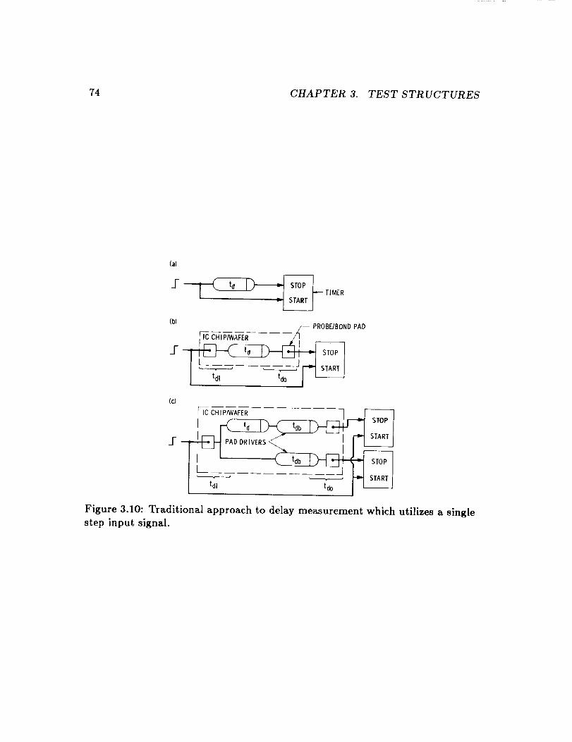
74 CHAPTER 3. TEST STRUCTURES
(a)
_r _ TIMER
(b)
_-- PROBE/BOND PAD
.rlC CHIP/WAFER /! __
(c)
[IC CH IP/WAFER '7
_l-
Figure 3.10: Traditional approach to delay measurement which utilizes a singlestep input signal.

3.2. TIMING SAMPLER ARRAY 75
accuracy through averaging.
The method shown in Figure 3.10a has limitations which are illustrated in
Figure 3.10b. In this case, a considerable delay, Qo, is introduced in driving the
output pad and the STOP input of the timer. This output delay could be up to
six orders of magnitude larger than Q. An additional delay tai exists at the input
of the ta element. However, this delay is very small compared to ta when the
input pad is driven from a low impedance source and the wire connection from
input pad to delay element is short. Thus, the timer will measure tdi + ta + tao,
which, since Qo >> tai + td, is approximately trio. To successfully implement
this method, the STOP input of the timer must present a minimum load (on
the order of a minimum size gate load) to the output of the delay element.
To accomplish this, the timer must be integrated onto the IC chip. This is
impractical, however, because of the timer complexity, size, and possible low
yield for the fabrication process.
An obvious solution to this problem would be to use two parallel delay paths
as shown in Figure 3.10c. Although each path contains a delay of ta_ + tao, only
one path contains td, so the difference between the two measurements would yield
Q. The problem with this measurement, however, is that we are subtracting two
large numbers (tab +tao >> ta) having a variability as large or larger than ta. This
variation in the fixed part of the delay (td_) in each path is a result of local process
variations on the chip. A further drawback, is that this circuit occupies a large
area on the chip due to the pad drivers.
Our timing sampler method of measuring on-chip delays circumvents the
problems associated with the methods just discussed. This method still uses
a timer for delay measurement, but does not connect the STOP input to the
ta-delay output. Instead, the STOP input is generated by an off-chip source.
The timing sampler method uses two input pads that are driven by off-chip
start and stop signals. The delay between start and stop signal transitions is
adjusted and accurately measured with a timer as shown in Figure 3.11. The
START input drives the td-delay input and the td-delay output is connected to
the timing sampler A-input. The timing sampler A-input presents a minimum
load to the ta-delay output. The timing sampler B-input is connected to the
STOP input pad.
The timing sampler functions as an on-chip transition skew detector. It
determines if the skew, or delay between transitions on inputs A and B, is
positive or negative. Thus, it answers the question: "Did the transition on
input A occur before or after the transition on input B?" Since the A signal is
delayed by ta and the B signal is not, the timing sampler output indicates if the
on-chip delay ta is greater tha.n or less than the input delay t,, applied between
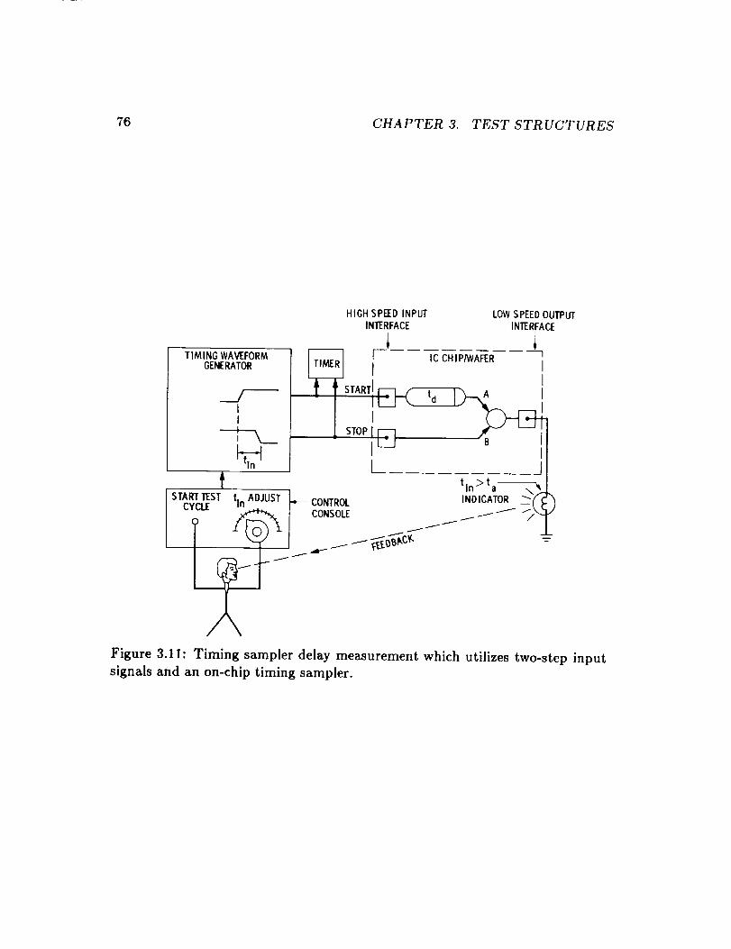
76 CHAPTER 3. TEST STRUCTURES
TIMING WAVEFORMGENERATOR
_
II
iS_,TTEST,. ADJUSTL__CONTRO_
CYC,_'_ I- CONSO,_j
HIGH SPFFD INPUTINTERFACE
L .....
jf
LOWSPEED OUTPUTINTERFACE
tln > ta_
INDICATOR "--_'_ )
.,I--
Figure 3.11: Timing sampler delay measurement which utilizes two-step input
signals and an on-chip timing sampler.
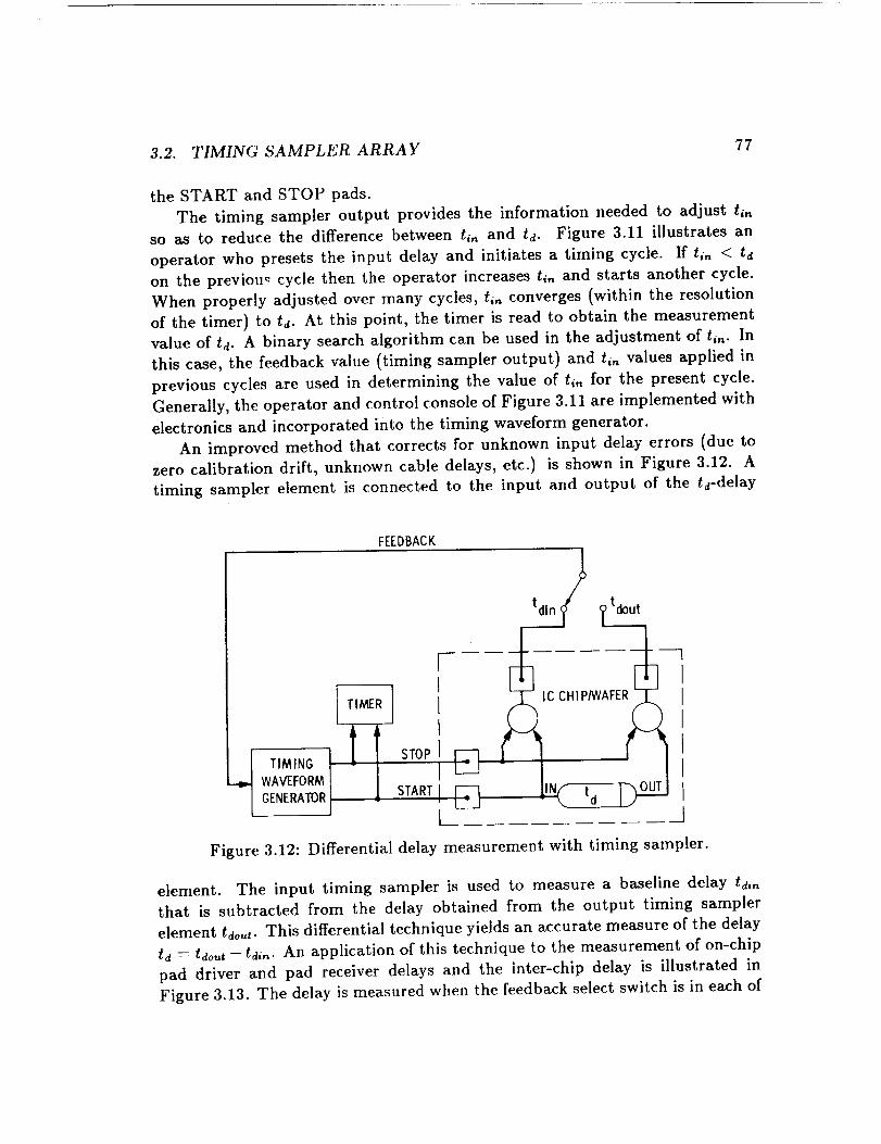
3.2. TIMING SAMPLER ARRAY 77
the START and STOP pads.
The timing sampler output provides the information needed to adjust ti,
so as to reduce the difference between ti, and ta. Figure 3.11 illustrates an
operator who presets the input delay and initiates a timing cycle. If t_, < td
on the previou_ cycle then the operator increases tin and starts another cycle.
When properly adjusted over many cycles, tm converges (within the resolution
of the timer) to td. At this point, the timer is read to obtain the measurement
value of ta. A binary search algorithm can be used in the adjustment of t,,. In
this case, the feedback value (timing sampler output) and t_, values applied in
previous cycles are used in determining the value of tin for the present cycle.
Generally, the operator and control console of Figure 3.11 are implemented with
electronics and incorporated into the timing waveform generator.
An improved method that corrects for unknown input delay errors (due to
zero calibration drift, unknown cable delays, etc.) is shown in Figure 3.12. A
timing sampler element is connected to the input and output of the ta-delay
FEEDBACK
i
I
TIMING - STOPI
t
E--I ,C CH,p/WAFE_ "-]
Figure 3.12: Differential delay measurement with timing sampler.
element. The input timing sampler is used to measure a baseline delay tdi n
that is subtracted from the delay obtained from the output timing sampler
element tao,t. This differential technique yields an accurate measure of the delay
ta = tao,,t - tdin. An application of this technique to the measurement of on-chip
pad driver and pad receiver delays and the inter-chip delay is illustrated in
Figure 3.13. The delay is measured when the feedback select switch is in each of

78 CHAPTER 3. TEST STRUCTURES
_o D I_ __-_ t
J START[---- RECEIVERJ
GENERATOR
L FEEDBACK
Figure 3.13: Measuring inter-chip delay.
3.2. TIMING SAMPLER ARRAY 79
the four positions. The difference between the position 1 and 2 measurements
is the delay of the chip 1 output pad driver. The delay difference between
positions 2 and 3 measurements is the inter-chip delay, and between positions 3
and 4 measurements it is the delay of the chip 2 input receiver.
3.2.3 Muller C-Element as a Timing Sampler
A timing sampler is a circuit whose output changes state if a transition on
one input occurs before a transition on the second input. A 2-input Muller
C-element is a circuit that behaves in this manner. The Muller C-element can
be constructed from a 3-input majority gate (a circuit whose output is high
when 2 or 3 of its inputs are high) by connecting one of the 3 inputs to the
output as shown in Figure 3.14. This circuit is a bistable device that is the
digital equivalent of a Schmitt trigger since its output displays hysteresis. The
C-element behaves as a 2-input AND gate when its output is low and like a
2-input OR gate when its output is high. The digital behavior of a 2-input
C-element is characterized by the transition diagram of Figure 3.14.
The C-element timing sampler can be used in the measurement of positive
or negative transition delays. Timing diagrams for the measurement of positive
transition delays using a C-element timing sampler are shown in Figure 3.15.
The measurement timing cycle consists of a setup phase and a measure phase.
The setup phase places the C-element into an initialized state. In this state, the
C-element will trip, thereby causing the output to change state when a transition
on input A occurs prior to a transition on input B. The setup phase consists
of resetting the C-element output and then arming the A input. For positive
transition delay measurement, this is equivalent to traversing through node 00
and then to node 10 on the transition diagram of Figure 3.14. For negative
transition delay measurement, the setup phase corresponds to traversing through
node 11 to node 01. The measure phase includes the input delay period (tin)
and the out period where the C-element output is sampled to see if it changed
state (indicating tin > td).
A practical CMOS implementation for the C-element is illustrated in Fig-
ure 3.16. This circuit is not constructed from a 3-input majority gate, therefore
the output is not static. The memory action of the C-element function is pro-
vided by the capacitance C. This capacitance primarily consists of the input
capacitance of an inverter connected to the output node. The output is driven
towards ground when n-channel MOSFETs nl and n2 are on (A and B both
high), and towards VDD when p-channel MOSFETs Pl and P2 are on (A and
B both low). When leakage paths are neglected, the output voltage remains

8O CHAPTER 3. TEST STRUCTURES
LOGICSYMBOL
OUT = OUT
IMPLEMENTATION USINGA 3 INPUTMAJORITYGATE
/-- NODES LABELED
__ / WITH INPUT(AB)
OOA_---.L---_,_O! _ BRANCHES LABELED/ _k_O J/'l "X _ WITH NEWOUTPUT
011 Ol NC_ II ) NC--NO CHANGE
I
TRANSITION DIAGRAM
Figure 3.14: Two-input Muller C-Element as a timing sampler.

3.2. TIMING SAMPLER ARRAY 81
STARTo._,,- DIGITAL NETWORK ]_ - OUT
STOP o
START
A
STOP
OUT
tin<tdpCYCLE: OUT DOESN'T CHANGE
I
-- SETUP _:_ NEASURE
I
reset arm _, delay _ oul
I
iI
r ii i
i i
ii i
0
I
1
I
_ out
Figure 3.15: Positive transition delay measurement using a C-Element.
fixed as long as the logic levels on the two inputs (A and B) are different. The
response of this circuit to step input signals is, to a first order approximation,
determined by the saturation current of the MOSFET in the charge/discharge
path having the smallest width-to-length ratio (W/L) and by the capacitance
C. The slew rate kc of the output to step inputs is given by kc = IDs_t/C, where
In,,, -- (1/2)KP(W/L)(VDD - VT) 2 is the saturation current of the MOS-
FET having the smaller W/L ratio, KP = #C_,= = #Oo=/(WL) is the intrinsic
channel conduction factor, and VT is the threshold voltage. To improve the
C-element response (increase the output slew rate), the capacitance C is made
as small as possible.
Because of the finite slew rate, the C-element output will not switch from one
rail (VDD or ground) to the other unless the delay from the rise/fall of input
A to the fall/rise of input B is greater or equal to VDD/k_. When the delay is
less than VDD/k_ then the output voltage may be a nondigital level (neither a
valid logic-0 or logic-I). If the C-element timing sampler output is used as an
input to on-chip logic such as a decoder (as on the CRRES chip timing sampler
array) then the decoder may produce invalid outputs and draw excessive cur-
rent. This can only be avoided by insuring that the output of the C-element is

82 CHAPTER 3. TEST STRUCTURES
VDD
A
V0
°2pl
A n2 iB o._$_.ii_nl C
CN)S INPLEMEgrATDN
I
1 _PI
' _VDD
I \\
I \
' ¥- GNDi i
0 VDD
kC
INITIAL INPUTS LOW
RESmNSE
ov0
LOGIC SYMBO L
A lII
B 1 'I
1', ,,_- VDD
0 I Ivi GND
i I
0 VDD
kC
INITIALINPUTS HIGH
RESPONSE
Figure 3.16: CMOS dynamic C-Element latch where k¢ is the slew rate (with
units of V/s).

3.2. TIMING SAMPLER ARRAY 83
always a valid logic level. A staticizer circuit can be used to restore a nondigital
value to a valid logic level (VDD or ground). The staticizer circuit is shown
in Figure 3.17 along with typical static and dynamic characteristic curves. The
GND
! ' lVDD
! Vil _>_Vol Vi2 _:,_ Vo2 _
5
_" 4
0
3
it 2
> 1
Figure
STATICCHARACTERISTICSOFSTATICIZER
o i
Vst= Vinv =2.12 VOLTS
!
2 3 4 5
Vil= V02 (VOLTS)
DYNAMICCHARACTERISTICSOFSTATICIZER
........... _........
•-. 2 _-;_i .............. : Vst
0 20 40 60 80 I00 120 140
TIME (NSEC)
3.17: Restoring the logic level of the C-Element with a staticizer.
staticizer consists of an inverter pair with week feedback (long channel trans-
mission gate). When the C-element initializes V_l to a voltage above/below the
switching threshold V,,t, the staticizer will drive this node through the feedback
element to VDD/ground. The staticizer output can still remain nondigital for
a long period of time (indefinitely if Vii is initialized exactly to Vu), so a cross
coupled transistor mutual exclusion circuit can be connected to the 1/-ol and Vo2
staticizer output nodes. The mutual exclusion circuit output does not begin
to change state until the staticizer is off balanced from its switching threshold
(metastable) point by at least one transistor threshold (11701 - Vow] > Vth which
is approximately 1 volt).
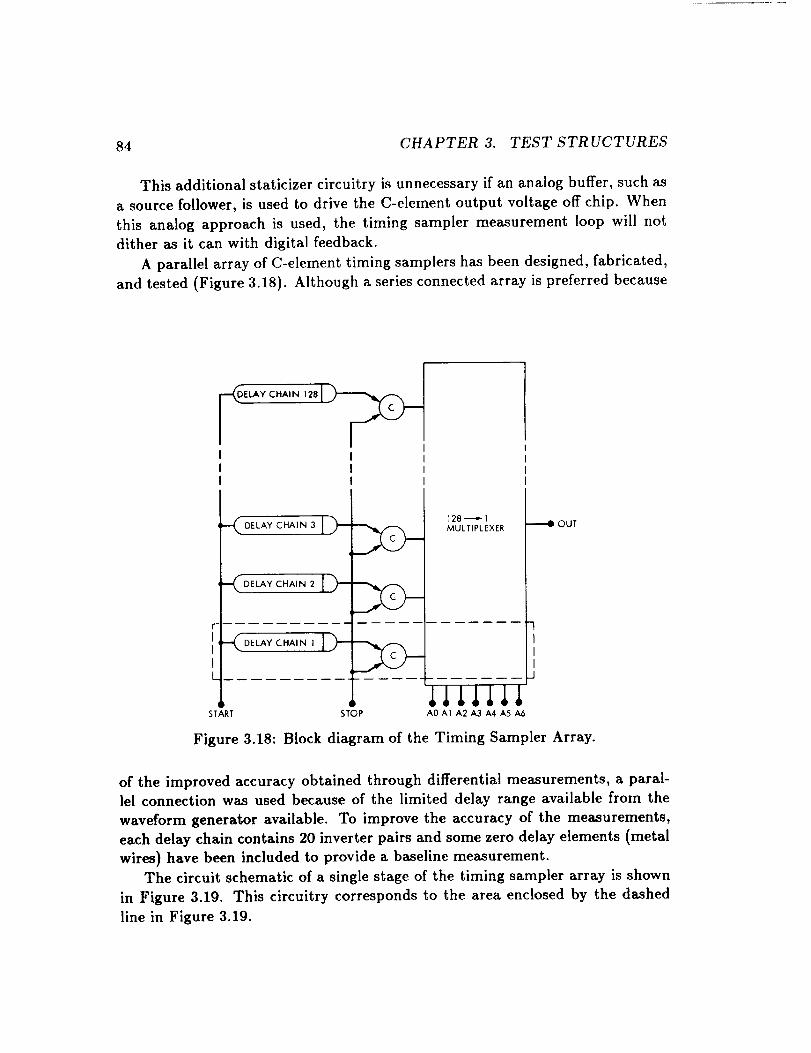
84 CHAPTER 3. TEST STRUCTURES
This additional staticizer circuitry is unnecessary if an analog buffer, such as
a source follower, is used to drive the C-element output voltage off chip. When
this analog approach is used, the timing sampler measurement loop will not
dither as it can with digital feedback.
A parallel array of C-element timing samplers has been designed, fabricated,
and tested (Figure 3.18). Although a series connected array is preferred because
---_E_Y CHAINL28J_____
-.._ DELAYCHAIN3 J )--- _(!!_,__
<DELAY CHAIN 2 JiI DELAYC.A,.;II
START STOP
128 ----_- IMULTIPLEXER
LLLLJ,,LJ,A0 A1 A2 A3 A4 A5 A6
OUT
Figure 3.18: Block diagram of the Timing Sampler Array.
of the improved accuracy obtained through differential measurements, a paral-
lel connection was used because of the limited delay range available from the
waveform generator available. To improve the accuracy of the measurements,
each delay chain contains 20 inverter pairs and some zero delay elements (metal
wires) have been included to provide a baseline measurement.
The circuit schematic of a single stage of the timing sampler array is shown
in Figure 3.19. This circuitry corresponds to the area enclosed by the dashed
line in Figure 3.19.

3.2. TIMING SAMPLER ARRAY 85
-(D.AYCHA,"']
IIIt
[
[
VDD
WEAK
FEEDBACK
TOR
r TIII
MULLER C-ELEMENT .L_
START SIOP OUT
_._ VDD /\/_ /\/
I _ I PULL-UP
MULTIPLEXER
Figure 3.19: One stage of the Timing Sampler Array.
3.2.4 Data Analysis
As-measured inverter pair data obtained from the timing sampler array, shown
in Figure 3.18, is displayed in Figure 3.20. This data comes from twenty inverter
delay chains which have transistors whose widths, W, and lengths, L, are dif-
ferent. The twenty transistor sizes used in the inverter delay chains correspond
to the points in the W vs. L plane whose as-drawn widths are 3, 4.5, 6, and
9#m and whose as-drawn lengths are 3, 6, 9, and 12/zm. In each inverter, the
p-channel transistor is the same size as the n-channel transistor; thus the ratio of
the p-pullup MOSFET to the n-pulldown MOSFET is r = 1.0. Also, the second
inverter of each inverter pair drives two equivalent inverters (fanout f = 2.0).
The X marked data points in Figure 3.20 correspond to rising (0 to 5V) output
transition delays, whereas the O marked data points correspond to falling (5 to
0V) output transition delays. Straight line segments have been drawn between
points of the same length.
A circuit tau model has been applied to the raw data. Figure 3.21 illustrates
the tau model applied to an inverter driving a fixed load capacitance CL. This
model states that the propagation delay of an inverter is proportional to the ratio
of the load capacitance CL to the gate capacitance of the charging/discharging
transistor (p-channel gate capacitance Cp for output rising edges/n-channel gate
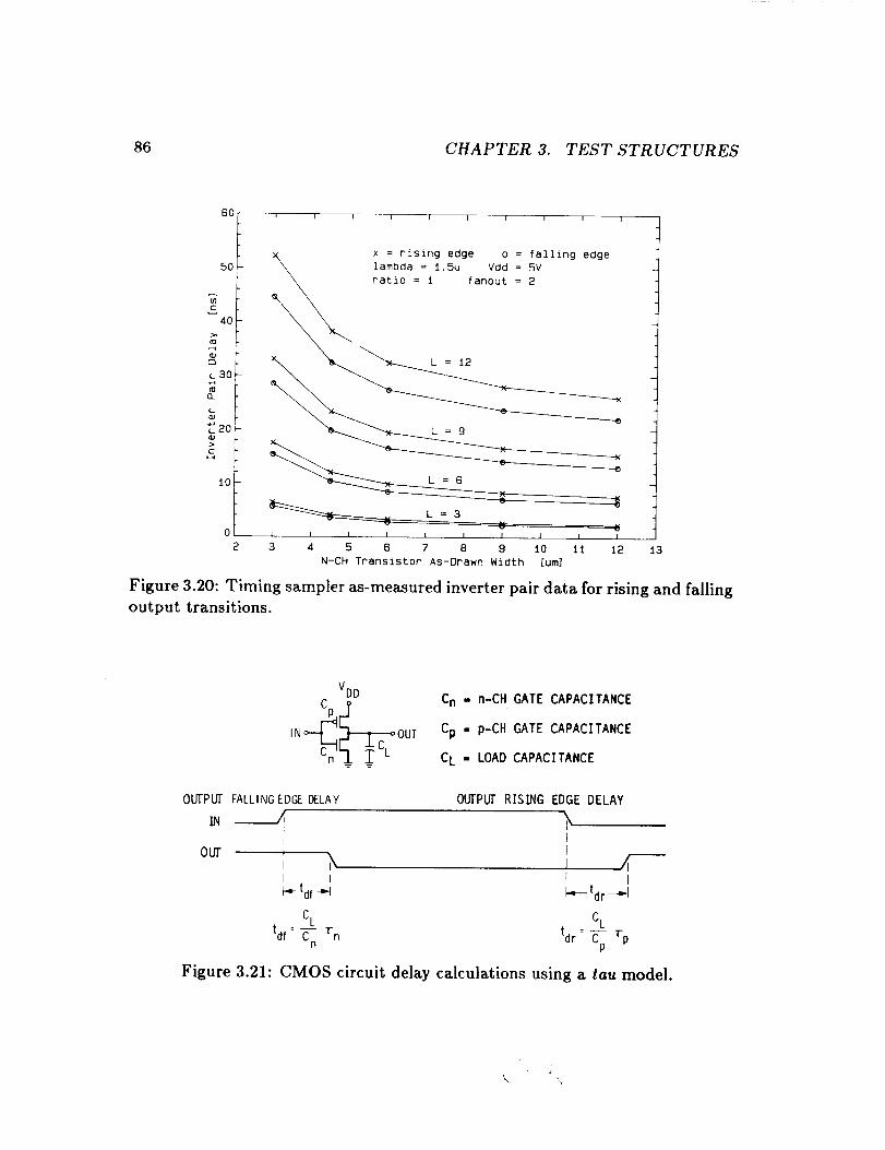
86 CHAPTER 3. TEST STRUCTURES
{30 _ I I T 3-- I I # I l
X, x = rising edge o : falling edge
50 _ lambda = i.Su Vdd = 5V
ratio = i fanout = 2
c40
L 30
Q_
aJ
_2o
c
lO
0 _ I I I t I I 1 I I
2 3 4 5 6 7 B 9 iO 11 12 13N-CH Transistor As-Drawn Width (um]
Figure 3.20: Timing sampler as-measured inverter pair data for rising and falling
output transitions.
VDD
CpCn . n-CH GATE CAPACITANCE
Cp - p-CH GATE CAPACITANCE
CL . LOAD CAPACITANCE
OUTPUT FALLING EDGEDELAY OUTPUT RISING EDGE DELAY
IN----./I
OUT _ I __, i', J /,r i 1 IP,,- tdf -,,H J-,,-- tdr
CL CL
tdf:_n n -r n tdr: _ p Vp
Figure 3.21: CMOS circuit delay calculations using a tau model.
I
, r

3.2. TIMING SAMPLER ARRAY 87
capacitance C, for output falling edges). The proportionality constant is r,_ of
the n-MOSFET for output falling edges, and _'p of the p-MOSFET for output
rising edges[2]. This results in an output falling edge delay ta/ = (CL/Cn)r,
and an output rising edge delay tdr = (CL/Cp)rp. A simple analysis of this
inverter circuit[2] shows that r is proportional to the square of the transistor
gate length, or r, - H,L_ and rp = HpL2p where the proportionality constants
are H, = 2VDD/[tt,(VDD - Vr,) _] for the n-channel MOSFETs and Hp =
2V DD/[#p(V DD-Vrp) 2] for the p-channel MOSFETs. H, and Hp are expressed
in terms of the n- and p-channel mobilities (/z,,,#p),and the n- and p-channel
threshold voltages (VT,, Vrp), and the power supply voltage V DD. This behavior
is illustrated by the data shown in Figure 3.20.
An interesting feature shown in Figure 3.20 is that, for a given length L,
the inverter pair delay increases as width W decreases. The reason for this
effect is that the load capacitance to gate capacitance ratio Ct./Cp or Ct./C,
depends on W. The load capacitance CL consists of the gate capacitance of the
MOSFET making up the inverters being driven as well as the interstage wiring
capacitance C,o. The MOSFET gate capacitances are proportional to gate areas
L×W: C, = eo_L,W,/To_ for the n-channel MOSFET and C_ = eo, LpWp/To, for
the p-channel MOSFET, where %, is the oxide permittivity and To, is the oxide
thickness. Referring to the inverter pair in Figure 3.22, the load capacitance
VDD
VDD VDD VDD
Figure 3.22: Timing sampler array inverter chain element.
at node '%" is CLa = C, + Cp + C_ and the load capacitance at node "b" is
CLb = f(C, + Cp) + C_b, where the fanout at node "b" is f = 2 (note: the fanout
at node "a" is f = 1). When considering output rising edge delays of inverters
consisting of transistors of constant length, the capacitance ratio CL/Cp consists
of a component that is independent of the width f(C, + Cp)/Cp and one that
is dependent on the width C_/Cp. It is this C_/Cp component that accounts
for the increase in the delay as the width decreases in Figure 3.20. Since Cp
is directly proportional to W, the inverter delay is proportional to 1/W. The

88 CHAPTER 3. TEST STRUCTURES
above argument applies to falling edge delays by replacing the denominator Cpwith C,,.
Another interesting feature of the data in Figure 3.20 is that for a given
length and width the rising edge delay is larger than the failing edge delay. This
can be attributed to the fact that the first inverter of each pair, which drives
node "a" in Figure 3.22, sees only one inverter input as a load (fanout = 1),
whereas the second inverter sees two inverter inputs as a load (fanout = 2),
and to the fact that p-channel transistors are slower than n-channel transistors
(Hp > H,, due to the differences in mobilities).
When the tau model is applied to the loaded inverter pair of Figure 3.22, the
following rising and falling edge delays are obtained:
1 Awa - Awb ]t_f = Hj, L2[1 + -r + rW-L ] + H'L2[f(1 + r) + WL'
where
and
A_a. 1 Awb ]tdr = H,_L2[1 + r + _{ + Hpi2[f(1 + r) +
CwbAwb --
C*o_
t Cp
- Ap._C'p + A._,_C L + A,,_C_
- ApbC_ + AmbCtm + AdbCld
C" C._ , CdCg_' Cd •Coz
L = Ln = Lp = Lo - A L, W = Wn = Wo - A W
Wp = rW,, Cp _ C_,,LWp Wp/Lp' c-.- c}:Lwo: ", w./L.......
The interstage wire capacitance is divided into three components: the polysilicon
capacitance (ApC_,), the metal capacitance (A,,_C,_), and the diffusion capaci-
tance (A_C_), where C_, C_, and C_ have units of capacitance per unit area and
Ap, A,_, and Aa are areas. Corrections are made to the as-drawn lengths/widths
(Lo/Wo) using AL/AW to obtain the true electrical lengths/widths (L/W). The
primed capacitance values, C_, C_, and C_ in the above equations have been
normalized by the oxide capacitance per unit area C_,, = eo,/To_ and are dimen-
sionless. Both of the equations for the inverter pair delays t4f and t_, can be
written as linear equations in l/W, where (W = Wo - AW). A fitting procedure
has been used to fit the as-measured data for rising and falling output edge

3.2. TIMING SAMPLER ARRAY 89
inverter pair delays (tdp and ta, as plotted in Figure 3.20) and the parameters
Lo, Wo, r, f, Ap_, A,_, Au,, Apb, A,_b, and Adb to the model equations to obtain! !
values for H,, Hp, AL, AW, Up, C,_, and C_. The finite difference Levenberg-
Marquardt algorithm was used in doing this fit. Figure 3.23 shows the results
S0
5O
.c4O
0Jo
L 30
n
c.
"220>c
10
i l i I i i
x = rising edge 0 = falling edge
Zarnbda = t.5_m Vdd = 5V L=11.72
ratio = i fanout = 2 _/^
Hn = 0.0157 ,HD.= 0.0284 //
Cp = 0.063 Cm = 0.253 Cd = 0.233 / Je
DELTAL = 0'281 __
L=2.72
0 I I I I I I
.06 0.14 0.22 0.30 0.38 0.46 0.54 0.62
I/N-CH Transistor Effective Width [1/#m]
Figure 3.23: Timing sampler fitted data where H is in units of ns/#m 2, W and
L are in units of #m, and C' is dimensionless.
of fitting the raw data to these equations. In this figure, the inverter pair data
is plotted against 1/W. The lines drawn through the data points are derived
from the model equations using the extracted parameters shown on the top of
the plot.The tau model fits the data very well considering its simplicity. The extracted
parameter C_, however, has an unrealistically high value. For the particular!
layout of the timing sampler, C_ should be less than C_ and Cp. The values
extracted for the three parameters C_, C_, and C_ are not accurate in a physical
sense because the changes in inverter pair delay due to the differences in metal,
polysilicon, and diffusion capacitance from one inverter chain to the next are
very small. This presents a problem in the separation of these parameters.

90 CHAPTER 3. TEST STRUCTURES
Another cause of this problem is that the periphery component of the diffusion
capacitance was not accounted for in the model.
3.2.5 Conclusions
The timing sampler is a compact test structure that allows fast, direct, and re-
peatable measurements of on-chip circuit delays. It overcomes the limitations of
the ring oscillator approach to delay measurement at the expense of some special
external hardware. The timing sampler delay measurement is also amenable to
wafer level measurements because there are no high speed outputs. Only two
high speed inputs need to be applied to the wafer and this is easy to accomplish
using coaxial cables and proper terminations on the probe card. Another posi-
tive aspect of the timing sampler is the ease with which it can be multiplexed.
The delay data obtained from a single compact timing sampler array can be
used to characterize gate delays over a range of device geometries employed in
typical circuit designs using the circuit tau delay model.
3.3 Proximity Structures
3.3.1 Introduction
The design rules, which are related to the spacing between different layers, are
not adequately tested by the common parametric test structures such as the
split-cross-bridge resistor, contact resistors, transistors, etc. To overcome this
deficiency, a set of very simple structures was developed and tested for the
CRRES fabrication run. These structures, which use only two pads and are
based on diode breakdown voltage, are termed collision test structures.
3.3.2 Structure Geometry
Figure 3.24 shows the geometry of the collision structures, with a cross section
shown of each. The distance d was varied from structure to structure. In every
case, d represents the "as drawn" dimension. It should be noted that because of
differences between fabrication processes, the actual physical dimension d could
vary between devices manufactured by different fabrication houses. The 'Active
region' shown in the cross sections refers to a thin-oxide region, such as the
source-drain junctions of a MOS transistor.

3.3. PROXIMITY STRUCTURES 91
..... °°,°
P-WELL
TO TO _ TO
PAD PAD PAD
I
ACTIVE ACTIVE ACTIVE
[] METAL i._i P-WELL
El ACTIVE • CUTS
:': p+ DIFFUSION,,.
Figure 3.24: Collision Test Structures for measuring p-well-to-diffusion (active)
and diffusion-to-diffusion breakdown voltage.
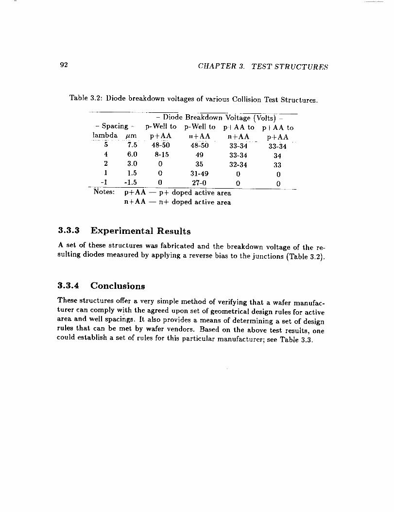
92 CHAPTER 3. TEST STRUCTURES
Table 3.2: Diode breakdown voltages of various Collision Test Structures.
- Diode Breakdown Voltage (Volts) -
- Spacing- p-Well to p-Well to p+AA to p+AA to
lambda /zm p+AA n+AA n+AA p+AA
5 7.5 48-50 48-50 33-34 33-34
4 6.0 8-15 49 33-34 34
2 3.0 0 35 32-34 33
1 1.5 0 31-49 0 0
-1 -1.5 0 27-0 0 0
Notes: p+AA -- p+ doped active area
n+AA -- n+ doped active area
3.3.3 Experimental Results
A set of these structures was fabricated and the breakdown voltage of the re-
sulting diodes measured by applying a reverse bias to the junctions (Table 3.2).
3.3.4 Conclusions
These structures offer a very simple method of verifying that a wafer manufac-
turer can comply with the agreed upon set of geometrical design rules for active
area and well spacings. It also provides a means of determining a set of design
rules that can be met by wafer vendors. Based on the above test results, one
could establish a set of rules for this particular manufacturer; see Table 3.3.

3.3. PROXIMITY STRUCTURES _ 93
Table 3.3: Design rules for manufacturer as indicated by Collision Test Struc-
tures.
Design Rule Name Design Rule Value
p-Well to p+Active Area
p-Well to n+Active Area
p+Active Area to n+Active Area
p-t-Active Area to p+Active Area
8.0/_m
7.0#m
3.0/zm
3.0/zm

ORIGINAL PAGE IS
OF POOR QUALITY
94 CHAPTER 3. TEST STRUCTURES
3.4 The Split-Cross-Bridge Resistor
1572 IEEE IRANSA('II()NN {JN ELI_CIRt)N DEVIfZI_S. VOL ED 33, N[) IO. O(I()BER IV8b
The Split-Cross-Bridge Resistor for Measuring theSheet Resistance, Linewidth, and Line Spacing of
Conducting Layers
MARTIN G. BUEHLER. MEMBER, IEEE, _.ND CHARLES W. HERSHEY
Ab_IrocI--A new lest _trncture _a_ developed ft_r evaluating the line
spacing bt'tween conductnrs on the _ame layer by using an electrical
measurement technique. This compact structure can also be used to
measure the _heet re_i,,tance, linewidth, rand line pitch of the cnnduct-
ing laser. I.ising an inlegraled-circuit fabrication prt_ess, Ihi_ struc-
ture _a_ fabricaled in difru_.ed pcdycry_lalllne sili_nn and metal layers.
Th¢_e _lru_ture_ _ere measured i,plieall) and rlectrically, and the_e
measured value were compared. For the lecrhnique_ u_,ed, Ihe optical
mei_urelneJil_ _ere typically one-quarter micromeler greater thin the
ele_lrieal measurements ftDr the pc_13,_ilicon and metal layers. Most
electrically measured line pitch valne_ were within 2 I/¢reent of Ihe
designed _ alum. A _mall difference between Ihe me=sured and designed
lint pileh i_ u_ed Io validale sheet resistance, linewidlh, and line spac-
ing _alne_. Ue_l results confirm the _lructure's _elf-cbecking _ature
based on the line pitch. Thai is, i small difference between the mea-
sured and designed line pilch is used to validate sheet resistance, Iine-
_idlh, and lir_ _paring values. Rule_ for designing abe lest _tructnre
are pre_nled in detail.
I. INTROI)U('I I[)N
HIS PAPER describes an approach to measuring the
sheet resistance, linewidth, and line spacing of elec-
trically conducting lines. The approach is an extension of
cross-bridge resistor I I I measurements and is based on an
electrical measurement technique in which the parameters
are determined from a specially designed cross-bridge re-
sis,or, termed the split-cross-bridge resistor. Alternative
techniques for measuring linewidth and spacing are based
on visual measurement techniques 121. The test structure
described here can be used to evaluate integrated-circuit
layout rules quickly and accurately. The technique was
demonstrated by fabricating 14 test structures in metal,
polycrystalline silicon, and diffused silicon layers. The
form of these test structures is shown in Fig. 1 and their
critical dimensions are listed in Table I.
To illustrate the measurement principle, consider the
polysilicon split-cross-bridge resistor shown in Fig. I,
which Was designed to evaluate the line spacing between
two polysilicon lines The split-cross-bridge resistor is a
combination of three structures. The upper structure is a
cross resistor, the middle structure is a bridge resistor, % - _0 _,
and the lower structure is a split-bridge resistor. The % " a'_ _"
j °r
Fig I Spilt crl_ss bridge re_islor designed I_1 evaluale Ihe linewidlh ½'.
line spacing S. and sheel resistance R, _la conducling layer
TABLE 1
SPLIT-CIIo_,S-BRI[XII_ RESISTOR CRITICal. DIIdENSIONS ANI) V_'II _AGE TAP
G_O_ETrlC_L ERI_ORS (E_)
Manus,:rlpt re°e,red December Ig. 1985. revised May I. 1986
The authnrs are with the }el Propulsion t a_ralol_y. California Instilule
of Techn,dog3,. Pasadena. CA 91109
IEEE Log Number 8610062
bridge resistor has a single conducting channel of width,
Wh = 2W + S. The split-bridge resistor has two con-
ducting channels, each with a width of W so that the ef-
fective width is IV, = 2W. The line spacing S is deter-
0018-9383/86/1000-1572501.00 © 1986 IEEE

ORIG/NAL P,_E; i3
OF. POOR QUALllV
3.4. THE SPLIT-CROSS-BRIDGE RESISTOR 95
BUEHt_ERAND HERSHEY SPI.IT.CROSS BRIDGE RESISTOR
mined by subtracting the width of the split-bridge resistor
(W, = 2W) from the width of the bridge resistor (W h =
2W q S)
II. MEASUREMENT TECHNIQUE
the technique requires three electric_al measurements,
which are illustrated by the following idealized relation-
ships. These relationships are uncorrected for geometrical
errors, which, as discussed in a later section, can be ig-
nored if the structure is designed properly, In the analysis,
the sheet resistance R, of the layer is needed, and this is
calculated from the cross resistor using the simplified van
der Pauw [3[, 14] equation
R, = tV.-/I,)tT/In 2> t])
where the potential difference V, is VL -- V 2 for a current
/, passed into I T and out of lF
The width of the bridge resistor is determined from the
idealized rectangular resistor expression
w h = 2W + S = R_LhlJVh (2)
where the potential difference Yh is V, - V_ for a current
Ih passed into/t and out of 1_. The distance between the
voltage taps is Lh, which is the distance specified on the
photomask. The sheet resistance R, is determined from
the cross resistor and (I). The width of the split-bridge
resistor is determined from
W, = 2W = R,L,I,/V, (3)
where the potential difference V, is V4 - V5 for a current
/, passed into Ii and out Of I_. The distance between the
voltage taps is L_. Note that the above equations require
that no significant magnification occur so that Lb and L,
can be taken as their design values.
The general expression for line spacing is
S = Wh - IV', = e,(Lb/hV, - L,I, Vb)I(V_V ,) (4)
where the sheet resistance R, is determined from the cross
resistor and (l).
For It, = 1, = I and Lt, = L, = L. then
S = R,LI(V, - Vb)ttVbV_) (5)
The [inewidth is calculated by modifying (3) and assum-
ingI, = landL, = L
W = R, LI/(2V,). (6)
Finally the line pitch P, between features is determined
from
P, = W + S = Wh - (W/2)
= R, LI(2V, - V_)/(2Vbl/O. (7)
Thus, the split-cross-bridge resistor can be used to eval-
uate four critical parameters of a conducting layer, i.e.,
sheet resistance, linewidth, line spacing, and line pitch.
Ill. MEASUREMENT INTERPRETATION
A physical model was developed that compares the
linewidths and spacings of photomasks or wafers features
1573
tLU$
lltcm -
Fig 2. Cross-sectional diagrams of a p.)lycr_slalltn¢ (poly) qlicon ta)erand a photomask where critical dtmenMons are indicated.
- r s_ -'t,
_1 -- $1 -rl -",llt,_ _1 "r,lt _
-I I -- tt -It7
1b1
Fig ] Cross sectional diagrams of two diffused layers formed (a) b:, auniform oxidation, diffusion, oxidation process and (b) by a local-oxi-dation, diff'asion, oxidation pt_ess where crmcal dimensions are tndl-caltd Intermediate surfaces a_e shov, n by dashed lines
measured by either visual or electrical techniques. The
size of a feature may expand or contract linearly due to a
number of factors, such as the bloating and shrinking of
features during photomask making or lateral etching, lat-
eral diffusion, and the coating of features of deposited
layers during wafer fabrication. The model requires the
use of the following eight parameters:
Wp. St, is the linewidth and spacing of a feature ob-
served visually on a photomask.
W_,, S,_ is the linewidth and spacing of a feature ob-
served visually on a fabricated wafer.
W,, S, is the )inewidth and spacing of a layer mea-
sured electrically on a fabricated wafer.V is the difference in the location of a feature
edge as determined from visual measure-
ments made on photomasks and fabricated
wafers.
X is the difference in the location of a feature
edge as determined from visual and electri-
cal measurements on fabricated wafers.
The relation among these parameters is shown in Figs. 2
and 3. Fig. 2 illustrates the fabrication ofa polycrystalline
silicon (poly) layer where the width of the poly layer ob-
served on the wafer (W, or W,,) is smaller than the width
(Wp) on the photomask. The visual width W,, is shown
arbitrarily at the base of the oxide, which surrounds the
poly layer. The electrical width IV, is shown at the mid-
point in the length of the trapezoid describing the poly
layer.

ORIGINAL PAGE iS
OF POOR QUALITY
96 CHAPTER 3. TEST STRUCTURES
1574
TABLE ]l
CfyMPARI'_ON OI [ANIwlDTHS aND SP_(INGS
IEEE tRANSACTIONS ON ELECTRON DEVICES. VOL ED]3, Nf) I0 OCTOBER 1g1¢6
II : _vaF I w/u2L
11 _ Isl II tTr 'k\
II al |1
Fig 4 The crn,r in measuring Ihe sheet resistance tr_m the Greek cro_s
due to shot1 arms Keeping A > 2 W ehrninales the get_melrtcal error
+n calculatin_ the ,heel re_i_lance from the van der Pau_ cqualion [5,
eq 11) t
Fig. 3 illustrates the formation of a diffused layer by
either I'1 a uniform oxidation, diffusion, oxidation process
or by 2) a local-oxidation, diffusion, oxidation process.
As illustrated in Fig. 3, the electrical width IV, includes
not only the planar portion of the diffusion but a fraction
of the lateral diffusion region as well.
The mathematical relationships among the eight param-
eters are illustrated in Table II. Note that the difference
between the upper equations for metal and poly structures
and the lower equations for diffused structures is the sign
reversal of the V and X terms. The measured quantities
W_, and W, are shown, along with three derived quantities:
W, - W+ (line spacing). W,12 (linewidth), and W_, IV,/
2 (line pitch). As can be seen in the table. IV, is larger or
smaller than IV, or We depending on the nature of the layer
being formed. For example, for a diffused layer, IV, is
larger than IV,, by 2V + 2X. Similar comments apply to
the line spacing. Such discrepancies are significant in
manufacturing processes.
The line pitch, W b -- (W,/2), listed in Table II deserves
special discussion. From the table it can be seen that IV,
+ S,. = W,, + $o = Wp + St,. This means that the linepitch measured electrically is a direct measure of the fea-
tures formed on the photomask That is. IV, + S, are not
affected by V and X because they are distances between
features that have the same kind of edge. For example.
W, + S,. is the distance between the left edges of two
parallel lines, and this distance is not affected by linear
changes in photomask features (bloating and shrinking) or
by wafer fabrication processes because both edges are af-
fected in an identical fashion provided features are not
magnified. If magnification can be ruled out. then W, +
S, can be used to verify that the design values for W and
S were correctly implemented on the photomask and were
measured correctly by the parametric test equipment. If
magnification (or a change in pitch) occurs, then the de-
sign value cannot be used for L_, and L, and the distance
between the voltage taps must be measured-visually.
IV. DESIGN CONSIDERATIONS
The design of the split-cross-bridge resistor follows
from four geometrical design rules. If these rules are fol-
lowed, then the equations given in Section II can be used
directly to obtain results that are accurate within one per-
cent.
The split-cross-bridge resistor was laid out so that it
could be probed with a 2 by N probe array 151where N is
an arbitrary positive integer. As illustrated in Fig. I, N =
4, and the probe pads are 80-#m squares separated by 80-
#m spaces.
The cross resistor is constructed from two equal-width
rectangles that intersect at right angles. Design rule #1
requires that the length A of each arm of the cross be at
least twice the arm width W in order for the sheet resis-
tance R_ to be calculated accurately from the idealized
sheet resistance expression [see (I)). This rule follows
from a detailed analysis of this structure 141; the result of
the analysis is shown in Fig. 4 The R, as calculated from
(I) is slightly less than the true sheet resistance, R,, as
given by
R_ = R.(I - E_) 18)
where E] is the geometrical error. By extralx)lating the
curve in Fig. 4, the error for A >= 2Wis seen to be
negligible.
As applied to the split-cross-bridge resistor, design rule
#1 requires that A > = 2W;, for the cross and bridge por-
tion of the structure. The A > = 2W_, (rather than A > =
Wb) rule was chosen to include the design of diffused
structures wh¢re lateral diffusion is a factor. Ira structure
has an excessively large lateral diffusion (such as a p-welt
in a CMOS process), the designer may have to calculate
a suitable A/W_, ratio to minimize errors.
The following discussion applies to both the bridge re-
sistor and the split-bridge resistor. Bridge resistors are
constructed from a conducting channel that is tapped in
two places along the length oftbe channel. There are three
design rules to be considered. They include the distance

ORIGINAL PAGE iS
OF POOR QUALITY
3.4. THE SPLIT-CROSS-BRIDGE RESISTOR 97
BUEHLER AND HERSH[_Y SPLIT-CROSS BRII_IE RESISTOR
O_ 1/11 _ 1 |1, 7,//|
! • ,R/ll t21
0 O1 17
_A
Fig, 5. The error m measunng Ihc line_idth Imm a briog¢ sti_cturc due
tO pc_orballon_, in lh¢ channel current flay, at the v_dtage lap_,.
between and width of the taps, the length of the taps, and
the location of the tap relative to a change in the channelwidth..
Design rule #2 requires that the width D of the voltage
taps be designed at the minimum width allowed and that
the distance L between the taps be large enough so that
the channel width can be calculated accurately from the
uncorrected rectangular resistor expression (W = R,L/R).
This rule follows from a detailed analysis of the bridge
resistor shown in Fig. 5.
This analysis is based upon the results of conformal
mapping described by Hall 161 where the length of the tap
is much larger than its width. His result [6. eq. (48) I in-
dicates that the resistance of a bridge between the voltage
taps is given by
R = R,(L/W)(I -- E_) (9)
where the geometrical error E z is
E 2 = (2W/rL)[(D/W) tan-I (D/2W}
- In(I + (D/(2W)):)I. (10a)
The uncorrected channel width is
W = (R JR) L ( 10b)
where L is the distance between the voltage taps and D is
the width of the tap. From this expression
W = W,/(I - E,3 (ti)
where W_ is the true channel width. This indicates that W,
as calculated from the idealized rectangular resistor equa-
tion (see (lOb)), is slightly larger than the true width W,.
The distance between and the width of the voltage taps
of the bridge resistors were chosen to reduce the geomet-
rical error to an acceptable amount. For the structures in-
cluded in this study, the width of the voltage taps was
taken as the minimum width allowed where L_ = 160 tun
and L_ = 140 ,urn. The errors for E 2 are listed in Table I,
where E:b is the error for the bridge resistor and E2, is the
error for the split-bridge resistor. The errors are worse for
the metal layer, but even for this worst case. the error is
less than one half of 1 percent.
1575
_v
t
_i " 1,
11
Fig 6 Re_or model o! uhc br}dge _trt/clurc u_ed io t'_lrma_c" ctror_ m
duced by bridge lap'_
Design rule #3 requires that the length G of a tap from
the current carrying channel be at least twice the width D
of the tap for the channel width W to be calculated accu-
rately from the uncorrected rectangular resistor expres-
sion (W = R,L/R). This rule follows from a resistor model
developed for the bridge as shown in Fig. 6 Each ma3or
area of the resistor is assigned an equivalent resistor that
is calculated from the rectangular resistor equation. The
objective of the model is to determine the parameter "'g."
which indicates the effect of the tap in diverting current
from the channel The resistor model leads to
R = R,[(L/W) E_] (12)
where
E_ = (D/W)/II + (W/gD)I (13)
The resistor model tap length is G* where G* = gD.
The parameter "g" was evaluated by finding a value
for g that provides a good fit between a plot _f E_ versus
D/W and an analytical expression derived from HaWs
equation 16, Eq. (48}1
E._ = (L/W)Ez = t2/r)[(D/W) tan I (DJ2W)
- In (I + (D/(2W))")I. {14)
This equation is applicable to the case where the tap is
much longer than its width and was derived from confor-
real mapping theory. Equation (13) is a very good ap-
proximation to (14) for g = 0. t8. This result indicates
that only a small fraction of the tap serves to shunt the
current from the main channel. The design rule requires
that the design tap length G > = 2D. This means that the
design requirement for G/D is I 1. I times larger than re-
quired by the model (G*/D = g = 0.18}. which should
minimize errors due to terminating the taps.
Design rule #4 requires that the edge of a voltage tap
be located twice the channel width from a change in the
channel width for the channel width W to be calculated
accurately from the uncorrected rectangular channel re-
sistor expression (W = R,L/R). As applied to the split-
cross-bridge shown in Fig. 1, this rule allows one to es-
tablish the distances H h and H, shown in the figure. This
rule follows from a detailed analysis of current flow past
a discontinuity in the width of the channel as shown in
Fig. 7. The analytical expression 161 for the current den-
sity J(x) along the r-axis is

ORIGINAL PAGE IS
OF POOR QUALITY
98 CHAPTER 3. TEST STRUCTURES
157h lEEk. tRANSA( tH)NS ()N Eli(IRON DEVICES. VOI. ED3_. NL) I(I. (X'IOBER Iqg6
27
_0- _ _ ,w[ ' ','
I(
P4 Q r "" ('Q'
"_-_'4'<>
FJ_ 7 ('un'enl denxH), ahmg Ihc NiItOlll edge of a conducting latyc[ Ihal
ahmplly _hange_ v_idlh Keeping voltage lap_ a distance that ix Iv, ice Ihe
_ldth ol the channel _rtHn the th_tt_nl_llLIl[}, nlinlltllIC_ Ihi_ error in cal
culaling the hn,:v, ldth tnmL tb)
whercfis the ratio of the width of the smaller channel to
the width ol the larger channel. The distance along the x-
axis is
_- = [in (a/h) ,fln (c/d)l/a- (16a)
a = _/-I +t + ,_1-_-let (16b)
¢,= ,;1 + t - I,_ + f>; (16c)
, : ,/i _/:, + r_q-_5 tl6d)
a_,/t +):7i /,/i + r (lbe)
where the parameters t and it that link the above equations
arc given by
t = exp(-2ul. (17)
These equations v, ere derived from HaWs equations 16,
eqs t40) and (41} I using the Iransfi_nna|ion 2 tanh _ (:.)
- Inl(l + z)/(l :_l.
The results shown in Fig. 7 indicate that the current
densit.', settles uut in a distance that is less than twice the
channel "_,idth from the discontinuity. This is tree for both
the small and the large channels. Notice that design rule
#4 is conservative wilh re_,pecl to the large channel, That
is. the 14" shown in Fig. 7 is one-half the width of the
bridge resistor.
V, EXPERIMEN'IAL RISUI.TS
Measurement procedures fbr evaluating the sheet resis-
tance and the electrical linewidth are detailed elsewhere
III, 131, 171. These procedures require the bridge voltage
to be measured for current flowing in both directions along
the channel This procedure is intended to eliminate errors
intrt_luced by voltage offsets due to instrumentation er-
rors and Ihermal voltages at switch relays. The elimina-
tion of such errors aSSUlnes that the current reversal is
accurate. Also. the sheet resistance as determined from
the cross resistor should result from the average of four
resistance measurements. One measurement requires cur-
rents to be forced in both directions between point I_ and
I: and voltages measured between V_ and V,. The other
measurement requires currents to be lotted in both direc-
lions between points 1_ and VI and voltages measured be-
tween V2 and I, 131. [7]. A minimum of eight resistance
values is required to measure R. W, S, and P, from the
split-cross-bridge resistor, In addition, the currents forced
through the structures must be adjusted to avoid various
interference effects such as self-heating. These effects are
discussed at length in [7]. Additional measurements can
be used to determine if any of these effects are a signifi-
cant factor.
The procedures for measuring the optical linewidth of
the layers are given below. The procedures were devel-
oped to minimize magnification errors associated with the
SEM. The test structures used for this comparison con-
sisted of 14 different split-cross-bridge resistors arranged
on a test chip. These structures were fabricated using a 3-
,am CMOS bulk process. Two sizes of structures were de-
signed for each of seven layers: metal layer, n _ diffusion
layer, p+ diffusion layer, n* poly layer on field oxide
(thick oxide), n" poly layer on gate oxide (thin oxide),
p+ poly layer on field oxide, and p' poly layer on gate
oxide. Two different manufacturers fabricated the test chip
and four test chips were randomly chosen from each run.
The linewidths on these structures were first measured
electrically and then optically, The electrical measure-
ments were made using an automatic data acquisition sys-
tem with a computer controlled wafer prober. For this
study, the test currents forced through each structure were
1 mA firr the polysilicon on gate oxide. 500-,aA for the
polysilicon on field oxide and n ÷ diffusion layers, 200
ttA for the p* diffusion, and 5 mA for the metal layer.
After measuring the structures electrically, the silicon
dioxide protective passivation was chemically removed
from each test chip to expose metal and poly linewidths
of the split-cross-bridge resistor patterns. In the process,
some of the thermally grown field oxide was removed
from the edges of the diffusion layer lines thus increasing
the apparent optical width of these lines. The amount of
this oxide removed was not strictly controlled and thus
varied from chip to chip. The lines of each structure were
then photographed using a SEM. The following proce-
dures were used m minimize magnification errors while
taking these photomicrographs.
All photomicrographs of each chip were taken in one
continuous session. At the beginning of each session a
photomicrograph was taken of an NBS linewidth standard
[81 at both magnification values (2000× and 5000 x) used
in this study. Once the session began, the high voltage
was never turned off and the chamber was never pressur-
ized and re-evacuated as this could affect the magnifica-
tion properties of the SEM. Magnification was selected
by a muhiposition switch only. Each discrete magnifica-
tion value was therefore calibrated by using an NBS stan-
dard. No image enhancement (such as electronic focus
compensation) was used. Instead. the NBS standard and
test structures were focused by moving the sample into
and out of the field of focus, since electronically changing
the focus could change the magnification to an unknown

3.4. THE SPLIT-CROSS-BRIDGE RESISTOR
ORIGINAL PAGE iS
OF POOR QUALITY
99
BUEHLER ANn HFRSHE'f SPI.ll ('RIISS BRIIX;_ RESISIOR
value. For this analysis we selected a SEM with a record
of electronic stability and low magnification drift.
For the purpose of obtaining clear pictures, all samples
were photographed at a tilt angle of 45 degrees to the elec-
tron beam. The tilt axis was perpendicular to all distances
being measured.
Two photomicrographs were taken of each split-cross-
bridge resistor structure, one of the wide bridge line and
one of the splh-bfidge region. The second photomicro-
graph thus contained two lines. Thus, a total of 224 pho-
tomicrographs (2 photos × 2 bridges × 7 layers × 4 chips
x 2 manufacturers) were taken of the structures providing
a potcntial 224 independent data points (one data point
per wire width). Some of the structures were damaged
when the oxide layers were removed. In addition, line-
width data from all structures with an electrically mea-
sured pitch error greater than 3 percent were considered
unreliable and not used. Therefore, only 199 of the pho-
tomicrographs were used in this analysis.
The linewidlhs were measured on the photomicro-
graphs using a vernier caliper and a magnifying lens. The
vernier pro'_ided readings in thousandths of inches. The
width of each line segment ,...,as measured in three places:
near the top and bottom and in the middle of the photo-
micrograph. This resulted in three or six measurements
from each photomicrograph depending on whether the
photo was of the bridge or split part of the structures.
The measurements from each photomicrograph were
averaged separately and an uncertainty for each average
was calculated based on the spread of the data. These un-
certainties were typically less than one half of 1 percent.
The averages for each of the NBS photomicrographs,
along with the certified distances for the NBS standard
were used to determine a multiplying factor for each chip/
magnification combination. These were then used to con-
vert the average values for each linewidth measurement
to a width in micrometers The averaged linewidth values
were then used to fit the data using an unweighted linear
least squares fit 191. A separate fit was calculated for each
layer from each manufacturer. These are shown in Table
III. A sample set of data points are shown with their least
squares fit line in Fig. 8.
Table Ill shows good agreement between the electri-
cally and optically measured linewidlhs for metal and poly
layers over a range of linewidths. The near unit)' slopes
(M} indicate that the given intercepts (B} are representa-
tive of the offsets for the range of linewidths studied. The
visual measurements are typically a quarter of a microm-
eter larger than the electrical measurements. The table also
shows a definite correspondence between electrical and
optical linewidth measurements of the diffusion layers.
Because the apparent diffusion linewidth was increased
when the oxide layer was removed, the offsets shown for
the diffusion layers are useful only as upper limits of the
expected offset. More elaborate techniques such as taking
cross sections of linewidth samples are necessary to de-
termine a more realistic expectation of offset values for
1577
p lll_ Ill_)l.llll ONJ
m)lMr)OITP* _atV Om lmm OZlO! ./
i lS /"°
i /¢/
- /
_J . tmooJrA." s points
o/
Fig 8 Vu,ual versus electrical linewtdth measuremenls ol p+ pt)ly or. Ihin
oxnde plolted along _*_th hnear least squares fit line The equalion Iorth¢
hne is given above the plol
TABLE Ill
V_*,I al P tl',, MI( R(IMF [I R',) Vt RSA: ¢, El t:ctNI( AL E (IS MIcrOMI rFrs)
LI_ _II)TH Rtt a11<P.",HIP P = ME + B _()r Spt I_-Cm)ss Bl_lt_;I _
R:- st_ r_lr',
Lnr,t M -,-., a -/- _o
,_- P_ _r_l_ ox_ 1.oo4*/-o.oo9 o_*/-_.o9
_. p_t_ ¸ _t_l_ _ l_l_*/-c._ o_6+,-ooa
the diffusion layers. Others have made similar compari-
sons between optical and electrical linewidth measure-
ments of polysilicon lines for the standard cross-bridge
resistor 110] and the Kelvin bridge test structure [11 ].
A comparison of electncal measurements with the de-
signed values of W, S, and P, is given in Table IV. The
data are based on measurements from four structures per
layer. The structures used for this comparison were the
smaller of the two split cross bridges on each layer from
one of the manufacturers. In order to provide a typical set
of measurement values, electrical values from all of these
structures were used regardless of deviations in line pitch.
which in some cases exceeded our 3-percent limit. As seen
in the table, the measured linewidth and line spacing val-
ues deviate significantly from the design values W o and
S_. In spite of this deviation, the mean line pitch errors
were less than half of 1 percent, and the measured line
pitch values P,_ were for most cases, within 2 percent of
the design line pitch values, P,0 = W_ + S 0. Thus the P,_
Pa_ values are useful in identifying bad data.
Vl. DISCUSSION
In order to calculate R, S. W, and P, from (1), (5), (6),
and (7"1. the split-cross-bridge resistor shown in Fig. I
must be designed according to the following layout rules.

ORIGINAL PAGE |3
OF POOR QUALITy
100 CHAPTER 3. TEST STRUCTURES
1578 IFI-t-: ]RANSACTIONS ON ELECTRON DEVICES, VOl. ED lb. NO 1O. OCTOBER 1996
TABLE IV
EXPtRIMI'qlA_ R_St LTS El F( I_I('AI A,_tlDkS_N 'V,_I t:F', ; _t_le.t SFIII
C_oss BRtt)GF R_ SISTOR',
Rule #1: The length A of the arm of each cross must be
at least twice the arm width We, (A > = 2WD.
Rule #2: The width D of the voltage taps of the bridge
resistor must be designed at the minimum
width allowed and the distance. L b and L,. be-
tween the voltage taps must be large enough so
as to minimize error E,; see Fig. 5.
Rule #3: The length G of the voltage taps from the cur-
rent carrying channel must be at least twice the
width D of the voltage taps (G > = 2DL
Rule #4: The distance H_, and H_ from the edge of a volt-
age tap to a change in the channel width must
be at least twice the width of the channel (tt,
> = 2W_,, /4, > = 2W,).
The experimental results obtained for this structure are
meant to demonstrate the "reduction to practice" of this
structure. The results are not meant to assure the user that
the structure will provide valid measurements for all pos-
sible linewidths and spaces. Some workers have sug-
gested that small lines will be overetched more than large
lines. If the etching is nonlinear in linewidth, the mea-
sured line pitch will not equal the design line pitch. This
inequality will alert the user to the discrepancy. Addi-
tional experimental studies are needed to confirm the use-
fulness of this test structure in measuring lines in the one
micrometer and smaller range. However. the results from
the cross-bridge resistor [10] would encourage the use of
the split-cross-bridge resistor in the submicrometer line-
width region.
Vii. CONCLUSION
The split-cross-bridge resistor is a compact test struc-
ture for measuring the sheet resistance, linewidth, line
spacing, and line pitch between various kinds of con-
ducting lines using electrical-measuremem techniques. A
model was developed to relate the electrical measure-
ments of linewidth and spacing to visual measurements.
According to this model, the electrical and visual tech-
niques give different results for the linewidth and spacing
measurements due to lateral diffusions and the coating of
layers. For a coated layer, the optical linewidth is larger
than the electrical lincwidth by about twice the thickness
of the coating. For pitch measurements, the visual and
electrical techniques measure the same quantity provided
features have not been magnified during the photomask
and wafer fabrication processes. If magnification can be
ruled out, then the electrical measurement of line pitch
can be used to assure thai R,. W. and S values were mea-
sured correctly. Fourteen kinds of test structures were de-
signed to measure the sheet resistance, linewidth, line
spacing, and line pitch of metal, poly. and diffused layers.
These structures were measured electrically and then op-
tically using a SEM. The optical measurements were typ-
ically a quarter micrometer greater than the electrical
measurements for the poly and metal layers. More so-
phisticated methods, such as cross section measurements,
are needed to determine the relation between electrical and
optical measurements of diffusion linewidths. The elec-
trically measured line pitch values are within 2 percent of
the design values for most cases,
ACKNOWLFDGMI-N !
Several staff members assisted in the development of
this project: C. Pina laid out the test structures. B_ Blaes
and H Sayah wrote the test programs, and H. Sayah ac-
quired the electrical data. Technical discussions with T.
Griswold and S. Suszko, both of JPL, D. Perlofl" of Pro-
metrix, L. Linhohn of NBS, P. Losleben of DARPA, and
the wafer fabrication se_ices of the Infimnation Sciences
Institute are gratefully acknowledged
REFERFNCES
I1_ M G Buehler. S D Grant. and W R Thurher. Br,dgc and van
tier Pauv. ,,beet re_i.,tnr,, t_r _h_act,:rlllt',g _he line v.idth of cotxduet
ing layers," J Ete(rrochem _,_ , _ol 125. no 4. pp 650 654.
Apr 1978.
121 D Nyyss0nen "'CaIibration of opt,cal systems fl)r line,._ldt_ men
suremems on '._afer_,' SPll-. _1 221. pp il9 126 1990
I31 L t van der Paul. Phthp_ Re_ Rep _1 I:_ p I. 1959. _lso tn
Phthp_ Teth Re_. vol 20. p 220. 1958
141 J M David and M G Buehler A numenc,d analysis of varltms
cross sheet resistor test ,,tnlcture_ ' Soltd.Shl_e Electron . v_ 20.
pp 539-543 1977
[51 M G Buehler. "Comprehensive test patterns _lth m(_tular test
slructures; The 2 by N probe pad array approach,_ Sohd Slate Te_h
nol . pp 99-94, Oci 1979
16] P M Hall, 'Resistance calculal_ons for thin film patterns.' Thin
Sohd Fdra.t. vol l. pp 277-295. 1967 1968
171 M G Buehler and W R Thurber. "'An experimental study of var
ioux cross sheet res_slor lest structure_." J E_e_tro, hera Soc. _oI
125. no 4. pp 645 650. Apr 1978
[81 B Ballard and F Ogburn. Nanonul Bureau o] Standards Certificate
Standard Reference Material 484h .Scatlmng k lectron Mtc ros( ope
Magnification $landard (elStage Me( rometer S_ale) Washington,DC. Natmnal Bureau ot Slandards. Nov 6. 1980
191 D C Baird. Erperimecita,on An Introduction to Mea_uremem The
or3 and Experiment Design Englewc, od Chfl'_. NJ Prentice-Hall.In..:. 1962.
[lOI L W Linholm. D Yen. and M W Cres_,c.ell. ' Eleclrical Ime_tdth
measuremem in lhe near- and suh-mleron ]tnewtdth region," in Pro(
3rd /at Syrup VLSI Integration Set acid Tethnol. pp 2gO-308.
1985
till T F Hasan and D S Perlnff. "Automated electrical measurement
techniques Io conlrnl VLS] Ilnev*tdlh. resistivity and registration.'"
Test & Measurement World. vol 5. pp 78 90, Jan 1985
3.4. THE SPLIT-CROSS-BRIDGE RESISTOR 101
BUEHt.ER AND HERSHE_r SPI.IT-CROSS BRIIX;E RESIST(IR
=i,
Martin G. Buehler (M'66_ received the B S E E
and MS degrees from Duke University and in
1966 received the PhD degree in electrical en-
gineering from Stanford UniverxiU,
Prior to joining the National Bureau of Stan-
dards in 1972. he v,,a,, i= _taff member of the Semi-
conductor Re,,earth and l)evehlpment Laborato-
ries, Texa_; |nstnlments, /no , where he ipplied
¢leclrical measurement techniques to the detection
of defects and the prolihng of dopants in semicon-
ductor materials At NBS he led a group in pro-
ces_i mc'trology, designed nearly a dozen semiconductor lesl structures, and
initiated a program on self-eeoc lechnique_ for VLSI He joined the Jel Pro-
pulsion Laboratory_ in 1981 and is now a Senior Re.arch Scientist. He is
currently the principal investigator of the Product A_surance Technology
Program for LSUVLSI and Ihe GaAs IC Dexlgn and product Assurance
Programs
t57_
Dr Buehler is a member of lau Beta PI. Et_ Kappa Nu, Sigma Xi, and
the Eleclmmechanical Sl_iety He wa_ awarded Ihc Department ot Cclm
merce's Silver Medal ftlr creattve contrihutitm_ tq_ semic,_ndu_lor melrc_l.
ogy while at the NBS
Char|t_ W. Her_he) i_ eurren¢_ v,,_rLing ¢,,_¢ard fhe F_ S degree frl h_th
phy',ic_ and electrlcalengmccrlng ,itlhe C,lhfi,rnlahl_tilute_f Tc_hn_l
ogy While _tudyin_ for h1_ bacheh_r_ degree he i_ _L_rklng at |he J¢l Pro
pulsion l.al_ratory m _n academic pan _in_c pl,_It_n m lhe V| SI Fe_h
noiogy Group


Chapter 4
Reliability Test Structures
PRECEDING PAGE BLANK NOT FILMED
103
m_GE /_',_ INTENTIONALLYBLANK

104 CHAPTER 4. RELIABILITY TEST STRUCTURES
4.1 Introduction
4.1.1 Electromigration
Electromigration is known to have detrimental effects on the reliability of in-
tegrated circuits. Therefore, test chips to measure the interconnect and con-
tact electromigration mechanisms have been designed and fabricated in 3-#m
CMOS/BULK for wafer level tests.
To test either type of electromigration test chip, it is placed on a temperature
controlled wafer chuck and stressed by a current source. A relay matrix is
used to bypass burned out segments. A computer controlled tester is used to
automate the entire test sequence including stress current application, resistance
monitoring, leakage monitoring and data recording. The test procedures for both
test chips have been developed and preliminary interconnect electromigration
tests have been performed.
4.1.2 Time-Dependent Dielectric Breakdown (TDDB)
In the TDDB studies the step-stress technique is employed to characterize the
reliability and integrity of the gate dielectric. The technique consists of a series
of constant field tests for a sequence of increasing field values and combines the
attributes of the constant field test and the ramped voltage test.
4.2 Layer Electromigration
4.2.1 Test Structures
Figure 4.1 gives the overall layout of the test structure. It is designed for a
2 x 20 probe pad array and consists of fifteen electromigration stripes connected
in series in the first and second metallization layers. The pad functions are listed
in Table 4.1 and the metal dimensions are listed in Table 4.2. Figure 4.2 shows
a cross section of the test structure, while Figure 4.3 shows an expanded view of
the two metal layers. At the end of each segment is a tap which is connected to
a double probe pad. Thus each segment contains a Kelvin contact which allows
accurate voltage measurements. The first layer stripes run perpendicular to the
second layer metal, thus providing a worst-case step coverage for the second
layer. The pattern of the poly layer is identical to that of the metal two layer.
This provides the steps for the metal one layer.

4.2. LAYER ELECTROMIGRATION 105
Figure 4.1: The electromigration test structure.
*:,:.:::::
LATOR
AL 1
SiO2
p-Si
Figure 4.2: Cross section of part of the electromigration test structure.

106 CHAPTER 4. RELIABILITY TEST STRUCTURES
Table 4.1: The Interconnect Electromigration Test Chip.
Pad # Name Pad # Name
1
3
5 M1
7 M2
9 M1,
11 M1,
13 M1,
15 M1
17 M1
19 M1,
21 M1,
23 M1,
25 M1,
27 M1,
29 M1,
31 M1,
33 M1,
35 M1,
37 M2,
39 M1,
Spare
M2, Extrusion Monitor
2
4
End L* 6
End L* 8
Tap 1 10
Tap 2 12
Tap 3 14
Tap 4 16
Tap 5 18
Tap 6 20
Tap 7 22
Tap 8 24
Tap 9 26
Tap 10 28
Tap 11 30
Tap 12 32
Tap 13 34
Tap 14 36End R* 38
End R* 40
Poly
M2 Extrusion Monitor
M1
M2
M2
M2
M2
M2
M2,
M2,
M2,
M2,
M2,
M2,
M2,
M2,
M2,
M2,
M2,
M1,
End L*
End L*
Tap 1
Tap 2
Tap 3
Tap 4
Tap 5
Tap 6
Tap 7
Tap 8
Tap 9
Tap 10
Tap 11
Tap 12
Tap 13
Tap 14
End R*
End R*
L = Left R = Right as seen in Figure 4.1
* Pads pairs 5 & 6, 7 & 8, 37 & 38, and 39 & 40 shown in Figure 4.1
are double pads to allow Kelvin measurement
Table 4.2: Dimensions of Metal Wires in Layer Electromigration Structure.
Layer Width Serpentine Length
Metal One 4.5gm 2.0cm
Metal Two 7.5 #m 1.0cm

4.2. LAYER ELECTROMIGRATION 107
10
9 C-
L
12
/
f_
11 Ix
Figure 4.3: Metal one and two layers of the electromigration structure. The
metal one wire snakes across the figure from left to right and the metal two
wire snakes from top to bottom. As shown in Figure 4.2, the polysilicon wire is
directly beneath the metal two wire to create worst-case steps for metal one.

108 CHAPTER 4. RELIABILITY TEST STRUCTURES
The extrusion monitor (pad 3 or pad 4) is intended to allow a check of the
minimum metal spacing design rule and to provide a test for metal extrusion.
Pad 2, which is connected to the poly layer, is intended to allow a check of the
insulation layers by measuring the leakage currents between layers.
4.2.2 Test Methods
The test procedure for the interconnect electromigration structure consists of
several steps:
.
.
Tests for leakage between the various layers. A voltage is applied to one
layer, and the leakage current from the other layer is measured, using the
extrusion monitor to test for shorts within layers (metal 1, metal 2, and
poly). Then the metal lines are tested for continuity. These tests are
designed to eliminate faulty structures.
Using a low current (1 mA), the resistance of each of the 15 segments is
measured.
3. The resistance measurements are performed at different temperatures.
. The desired stress temperature is set, the stress current is applied, and the
segment resistance is measured and compared with the segment resistance
measured previously to determine the actual metal temperature.
During the stress a high current is forced through all fifteen segments. The
output voltage of the current source is then monitored. An open segment causes
the current source voltage to reach its compliance limit. When a segment opens,
its position is determined by locating the voltage transition. In addition to the
above measurements, the resistance of each segment under test is measured at
one-minute intervals.
4.3 Contact Electromigration
4.3.1 Test Structure
The contact electromigration test chip consists of a total of sixteen different
structures having four sizes of square contacts (3.0, 3.3, 3.6, and 3.9 _m on a side)
and four contact-to-diffusion spacings (1.5, 2.25, 3.00, and 3.75 #m). A typical
structure, shown in Figure 4.4, consists of eight separate p-wells connected to

4.3. CONTACT ELECTROMIGRATION 109
'-'I 1-1 I,II
I
I
IIL
CONTACT
PAIRS
I'I 1"1 I!
II
I
CONTACT
TO WELL
(a)
VOLTAGETAP
IL D THIN-OX/DIFFUSION
r-'_ p-WELLL.J
;'": p+_,,:
R CONTACT
[] METAL
(b)
Figure 4.4: The metal-n+diffusion contact electromigration test structure.

110 CHAPTER 4. RELIABILITY TEST STRUCTURES
the even-numbered pads 4 through 18. Each p-well contains an n+diffusion
with contacts on each end. Current is forced between pads 1 and 20. The odd-
numbered pads 3 through 19 provide taps to the metallization stripes between
the p-wells which are used to monitor the resistance of each segment and also
to bypass a failed segment. Aluminum spiking and the resultant reverse-bias
junction leakage is monitored using the p-well contacts.
4.3.2 Test Method
To test these structures, a check of the leakage current is made for each set of
contacts contained in the individual p-wells to detect initial faults. If the struc-
ture is found to be free of faults, a stress current is forced through the contact
chain at elevated temperature. On regular intervals (3 minutes) the stress is
interrupted and the n+ to p-well leakage current and the contact resistance of
each pair of contacts is measured. If a leakage exceeds 1 #A or the resistance is
found to have increased by a factor of 2.0, the contact pair is considered failed.
The failed contact pair is then bypassed through an external switch matrix and
the test continued.
4.4 Time-Dependent Dielectric Breakdown
4.4.1 Test Structure
The Time-Dependent Dielectric Breakdown (TDDB) structure consists of two
side-by-side structures each probed by a 2 × 20 padblock as seen in Figure 4.5.
There are 76 sub-structures, where half are n-channel and half are p-channel.
These structures are essentially ganged arrays of MOSFETs. As shown below,
a large number of theses structures must be measured in order to acquire a
statistically significant amount of data.
The test structure also contains several large geometry gate oxide capacitors
to measure the gate oxide thickness.
4.4.2 Test Method
The test structures are first screened at low voltage (3 to 5 V) for shorted ca-
pacitors which are then excluded from the life test experiment. The criterion
for shorted capacitors varies with the size. oxide thickness, and other character-
istics of the test device. Typically, a gate oxide leakage current in excess of one
nanoampere indicates a dielectric failure.

4.4. TIME-DEPENDENT DIELECTRIC BREAKDOWN 111
_lr'lr'lt:lr'lr'll_l=l_0001 30000o_ 00000000000_
Figure 4.5: The time-dependent dielectric breakdown structure. This structure
consists of two arrays, each addressed by a 2 x 20 probe pad array found in the
center of the structure. Thus two probe set-downs are required to measure the
76 capacitors (38 n-channel and 38 p-channel) in this test structure.

112 CHAPTER 4. RELIABILITY TEST STRUCTURES
For TDDB evaluation we use the step-stress technique [20,21]. This tech-
nique combines the conventional TDDB and the ramp breakdown measurements.
For a set of oxide field values El, E2, .... , En arranged in increasing order, the
field E1 is applied to the test structure consisting of a set of 38 large capaci-
tors. The stress is interrupted after cumulative times of, say, .01, .1, 1, 10, and
100 seconds and the individual capacitors are examined for dielectric failure.
The failure data are recorded and the failed devices are disconnected using an
external switch matrix after each interruption of the stress. This procedure is
repeated for all of the field values in the set. As an example, the values 4.5, 5.5,
6.5, and 7.5 MV/cm constitute a reasonable set for this purpose. At the higher
fields (about 7 MV/cm and above), however, the breakdown mechanism changes.
At high electric fields, oxide conduction is dominated by Fowler-Nordheim cur-
rents. This introduces failure modes not present under circuit use conditions.
Therefore, caution must be exercised in the analysis of high field data.
4.4.3 Analysis Method
It has been experimentally observed that the time-to-failure distribution for the
gate dielectric at constant field exhibits a log-normal behavior and thus, on a
log-normal plot, it is represented as a straight line. Further, it has been shown
that if the stress field is varied this distribution changes only in the value of
the median-time-to-failure, ts0, and is otherwise unaffected. The extent of the
change in ts0 in response to the change in the field is given by the acceleration
factor, ff [22]. If ff were known, the step-stress data could be reduced to a
sequence of equivalent times-to-failure under the normal operating field (or any
other field). As discussed above, the data should then give a straight line on
a log-normal plot. Therefore, one can resort to a parameter fitting algorithm
to determine the acceleration factor. The analysis simply involves locating the
value of _/which best fits a straight line to the entire data set. Therefore, only
one parameter, the acceleration factor, needs to be fitted. Once the value of this
parameter is established, the standard deviation, o, and ts0 of the distribution
can be calculated.
Fortran codes were written to analyze the results of the step-stress experi-
ments. The program was subsequently tested for stability and sensitivity using
modeled data with known parameters. They were calculated using a random
number generator. These data simulate the results of the experiments conducted
on a sample population of finite size with the assumed values of the failure pa-

4.4. TIME-DEPENDENT DIELECTRIC BREAKDOWN 113
Table 4.3: Examples of modeled data for the step-stress oxide breakdown ex-
periment. The assumed parameters are: "7 = 7.6, a - 11.6, E0 - 1MV/cm,
and tso = 1.7× 10¹⁹s. For these values lnts0 =44.3and tl= 1 year. For the
numbers picked, time to 1% failure just happened to come out equal to one year.
E -- Cumulative Time (s} --
(MV/cm) 0.01 0.1 1 10 100
Exact
SO: 4.5 0.02725 0.04232 0.06352 0.09219 0.12948
5.5 0.12282 0.15052 0.19311 0.25087 0.31788
6.5 0.32349 0.35234 0.41632 0.49338 0.57202
7.5 0.57817 0.60878 0.67143 0.73845 0.79862
Sample Size = 3200
SI: 4.5 0.03625 0.05063 0.07344 0.10219 0.13969
5.5 0.14281 0.15656 0.20437 0.26156 0.33781
6.5 0.34250 0.37062 0.43281 0.50625 0.58594
7.5 0.59219 0.62094 0.68500 0.75281 0.80813
$2: 4.5 0.02688 0.04094 0.06344 0.08781 0.12562
5.5 0.12781 0.14312 0.18844 0.25375 0.31813
6.5 0.32344 0.34969 0.41625 0.49469 0.56875
7.5 0.57500 0.60281 0.66219 0.72938 0.79188
$3: 4.5 0.02313 0.04156 0.06344 0.09281 0.12344
5.5 0.12500 0.14375 0.18375 0.24469 0.30750
6.5 0.31406 0.34219 0.40531 0.48000 0.56000
7.5 0.56500 0.59406 0.65500 0.72688 0.79500
rameters 7, a, tso, and a failure distribution given by
f(ln t)_ av/_l ,['"t-ooexp (- lnt'-lntso+a(E-2o E°))dlnt'
where E is the oxide field and E0 is some reference field taken for simplicity to
be the operating field. It can be argued that the oxide field factor should be in
the form of lIE.
The data contains the purely statistical noise that is present in real data
due to finite sample size. Table 4.3 gives an example of modeled data sets, Si,
calculated by introducing random noise. The set So is from an exact (not ran-
domly generated) calculation based on the assumed values for the parameters
and corresponds to the case of an infinite sample size. For the other sets the

114 CHAPTER 4. RELIABILITY TEST STRUCTURES
Table 4.3: Examples of modeled data for the step-stress oxide breakdown ex-
periment. The assumed parameters are: "7 = 7.6, a -- 11.6, Eo = 1MV/cm, and
tso --- 1.7 × 10¹⁹ s. For these values In ts0 = 44.3 and tl = 1 year (Continued).
E- ........... Cuiimiativ_Time (s} ....(MV/cm) 0.01 O.1 1 10 100
Sample Size = 1600
$4 4.5 0.02313 0.04812 0.07312 0.10063 0.12500
5.5 0.12562 0.13875 0.18000 0.23937 0.30187
6.5 0.30687 0.33812 0.40250 0.47938 0.55250
7.5 0.55687 0.59000 0.66188 0.72562 0.79250
$5 4.5 0.03625 0.04750 0.07250 0.10250 0.13500
5.5 0.13750 0.15188 0.19437 0.24125 0.30750
6.5 0.31500 0.34000 0.40437 0.48625 0.57000
7.5 0.57437 0.60562 0.66938 0.74063 0.79562
$6 4.5 0.02437 0.04188 0.06000 0.09375 0.13375
5.5 0.13750 0.15687 0.19125 0.25125 0.30812
6.5 0.31563 0.34563 0.39562 0.47813 0.55937
7.5 0.56687 0.59938 0.65875 0.72750 0.80125
Sample Size = 800
$7 4.5 0.01875 0.02875 0.04000 0.05625 0.09000
5.5 0.09500 0.10750 0.15000 0.20500 0.28125
6.5 0.28750 0.31125 0.36875 0.46375 0.53875
7.5 0.54625 0.57125 0.64625 0.72875 0.80000
$8 4.5 0.02625 0.04000 0.06500 0.09250 0.12500
5.5 0.12750 0.15875 0.19375 0.24125 0.30875
6.5 0.31625 0.36125 0.41750 0.48125 0.55625
7.5 0.56250 0.59625 0.65500 0.73000 0.79500
$9 4.5 0.02250 0.03125 0.04375 0.06500 0.11125
5.5 0.13375 0.13250 0.17125 0.23000 0.30750
6.5 0.31125 0.33750 0.39625 0.49125 0.58000
7.5 0.58375 0.60625 0.66625 0.72625 0.78500
S10 4.5 0.02625 0.04000 0.05875 0.08000 0.11625
5.5 0.12000 0.13250 0.16625 0.22500 0.28875
6.5 0.29375 0.31625 0.39250 0.47000 0.56250
7.5 0.56625 0.59625 0.66500 0.74875 0.80625

4.4. TIME-DEPENDENT DIELECTRIC BREAKDOWN 115
Table 4.4: Results of the analysis of modeled data in Table 4.3. The assumed
parameters are: "7 = 7.6, a = 11.6, and tso = 1.7 x 10¹⁹s. For these values
In tso = 44.5 and tl = 1.0 year.
Sample Data Low High Passes "7 a tso tl Eo Sig.
Size Set '7 "7 (seconds)) (Years)_ - MV/cm __ Figs.Exact SO 6.48 9.19 308 7.6 11.6 44.3 1.0 1 6
3200 $1 5.21 9.60 335 8.0 12.3 45.7 0.8 1 6
3200 $2 5.79 9.72 311 7.6 11.6 44.4 1.2 1 6
3200 $3 5.41 9.52 290 7.4 11.3 43.2 0.7 1 6
1600 $4 4.79 12.32 309 7.5 11.7 44.3 0.8 1 6
1600 $5 5.09 10.40 295 8.0 12.7 46.9 1.1 1 6
1600 $6 4.24 10.57 323 7.1 11.0 42.5 0.7 1 7
800 $7 4.85 10.21 340 8.1 11.4 48.1 75 1 6
800 $8 5.46 10.15 304 7.7 11.9 45.1 1.2 1 6
800 $9 3.08 11.10 301 7.8 11.2 45.5 8.8 1 7
800 S10 4.80 10.31 291 8.0 11.9 47.2 9.5 1 7
corresponding sample size is given in Table 4.3. For each sample size, the simu-
lations were run a number of times. For the sample size = 3200, the simulations
were run three times and each run noted as S1, $2, and $3.
The results of the computer analysis of these data sets are given in Table 4.4.
The table groups the data sets by the sample size and in the second column
the data sets are identified (So, $1, etc.). The range in which the program
searched for the optimal value of the parameter is given by low and high
which is determined by a zero order consideration of the data. The number of
passes in the optimization algorithm and the resulting 7 are listed in the next
columns along with the corresponding values of a and ts0. The last column
gives the algorithm's estimate of the accuracy of the obtained "_ stated in terms
of significant figures. In addition there is a column for the parameter tl. It is
defined as time to one percent failure. In the study of device reliability we are
really interested in the low probability region, one percent or smaller. Therefore
tl is a more relevant parameter for comparison purposes.
Values for the various Sn are shown in Table 4.4. As can be seen, the values
for the S_1 vary further from the exact value of 1 as the sample size decreases.
This is due to the introduction of statistical noise into the data to simulate the

116 CHAPTER 4. RELIABILITY TEST STRUCTURES
finite sample size of the actual experiments.
One important variable in designing this type of experiment is the required
sample size for statistically meaningful results. Using tl as the figure of merit,
one observes that for sample sizes of 3200 and 1600, reasonably accurate results
can be deduced from the data. An experiment based on 800 samples, however,
yields results that may be in error by one or two orders of magnitude.The conclusions drawn from these exercises are that the algorithm is able to
perform the data analyses and appears to provide meaningful results for sample
sizes of 1600 or more capacitors (40 test chips minimum). If it is found that
n-channel and p-channel oxides are sufficiently alike, the data from both can be
combined and only 20 chips are needed.
4.5 Summary of Results and Future Work
Test structures for the study of interconnect electromigration and contact elec-
tromigration have been designed and fabricated. Software for automated stress
testing of both structures has been developed and debugged. Preliminary test-
ing of the interconnect electromigration structure indicates that a localized self-
heating effect is influencing our test results: further investigation is required to
resolve this problem and obtain improved results. No test results are available
for the contact electromigration structure.

Chapter 5
Device Models and Simulation
117

118
5.1
CHAPTER 5. DEVICE MODELS AND SIMULATION
MOSFET Subthreshold Parameter Extrac-
tion
5.1.1 Introduction
The extraction of parameters in the subthreshold region is needed to model the
leakage currents in SPICE simulations. In addition, the radiation effects com-
munity requires a standardized procedure for evaluating the radiation-induced
interface oxide trap densities [23]. The purpose of this effort is to develop a
standard analysis approach and to show that it is compatible with SPICE-like
MOSFET models. The extraction method developed here separates the inter-
face trap terms from body effect or bulk dopant terms and thus allows a more
accurate evaluation of the interface state and oxide trap densities.
In this effort, we restrict our view to MOS structures where radiation induces
oxide charge and creates oxide-silicon interface states but does not remove car-
riers from the bulk. These effects shift the threshold voltage and increase the
leakage currents of MOSFETs. In order to facilitate the analysis, two reference
cases were chosen and these are shown in Figures 5.1 and 5.2. For the p-MOS
reference case, shown in Figure 5.1, radiation induces positive oxide charge and
+ ++ +
+ + +m oW,,oo1110
GATE
OXIDEHOLETRAPS
•*--DONORINTERFACETRAPS]_-p-CHANNELHOLES•DEPLETEDn-SILICON
NEUTRALn-SILICON
Figure 5.1: The p-MOS reference case.
positive donor interface states. For the n-MOS reference case, shown in Fig-
ure 5.2, radiation induces positive oxide charge and negative acceptor interface
states [231 .
The threshold voltage for a "fat" FET, where short and narrow channel

5.1. MOSFET SUBTHRESHOLD PARAMETER EXTRACTION 119
-b -P .p
® ® ® ®
®o®o®ooo
GATE
OXIDE HOLE TRAPS
,,-'-ACCEPTOR INTERFACE TRAPS_'n-CHANNEL ELECTRONS
DEPLETED p-SILICON
NEUTRAL p-SILICON
Figure 5.2: The n-MOS reference case.
effects are negligible, is:
VT fb = VTo + FV/2¢f - VB (5.1)
where "fb" denotes a fat FET with back-gate bias, VB. For the n-MOS reference
case
YTo = 2¢f - Yot + Yit (5.2)
and for the p-MOS reference case
VTo = 2¢f + Vot + Vit
The threshold voltage for a fat FET without back-gate bias is:
VT fO = VTo + FV_
(5.3)
(5.4)
In the above expressions, 2¢f is the built-in potential due to the body doping, F
is the body effect term, and Vit is the potential due to the interface state charge.
Vot is the potential due to trapped oxide charge, interface implant charge, and
the gate-silicon work function.
The values associated with the radiation-induced quantities, Vot and Vit,
are positive when the sign of the induced charge conforms to the reference case.
A negative sign for either Vot or Vit signals the buildup of charge with a sign
opposite to that shown for the reference case. The following text is developed
for the fat FET where VT : VTfb.
The effect on the subthreshold current of the buildup of radiation-induced
charge is illustrated for a p-MOSFET in Figure 5.3 and for an n-MOSFET in

120 CHAPTER 5. DEVICE MODELS AND SIMULATION
RADLEVEL el _ VTfO(el) "1
["2q'_ --_2 e f'-_[-----Vit =1RADLEVEL e2 VTf0(e2)
LOG(IBinv)
LOG(IB)
LOG(IBmg)
GATEVOLTAGE,VG
Figure 5.3: Subthreshold characteristics for a p-MOSFET at radiation levels
¢2 > ¢1. The dashed line indicates how the characteristics shift if Vot changes
and Vit does not change with radiation.

5.1. MOSFET SUBTHRESHOLD PARAMETER EXTRACTION 121
_--_-F_/2$ f _1--2 _ f-_'_Vit_"_
RAD LEVEL _I I VTf0(_I) =I= -Vot-_
_I_F2-,_ _I 2_f_,J vit-----I=I = -Vot |RAD LEVEL OZl._VTf0(e2 ) I
LOG(IBinv)
LOG(IB)
LOG(I Bmg)
GATE VOLTAGE, VG
Figure 5.4: Subthreshold characteristics for an n-MOSFET at radiation levels
¢2 > ¢1. The dashed line indicates how the characteristics shift if Vot changes
and Vit does not change with radiation.

122 CHAPTER 5. DEVICE MODELS AND SIMULATION
GATEG'=G
VG_...__
UG
DRAIND'
IDIB
IA
,CloVD UD
S'SOURCE
BODY
B'=B
Figure 5.5: The model of an n-MOSFET where the drain and source resistance
is R. The subthreshold leakage current passes through the drain-source diodes.
Figure 5.4. These schematic semi-log plots of body current versus gate voltage
illustrate how the subthreshold current varies between the onset of inversion
(IBinv where VG = VT) and the condition where the Fermi level is located at
the middle of the band gap (IBmg where VG << VT). When the Fermi level
is at mid gap traps are uncharged; whereas at the onset of inversion, where
VG = VT, traps are fully charged. For the p-MOSFET, the buildup of positive
oxide traps and positive interface traps causes the IB curve shown in Figure 5.3
to shift to higher gate voltages with a smaller slope. For the n-MOSFET, the
buildup of positive oxide traps and negative interface traps causes the IB curve
shown in Figure 5.4 to shift to smaller gate voltages with a smaller slope.
In the model for the MOSFET shown in Figure 5.5, the measured drain
current, ID, enters the extrinsic drain tap, D t, splits into the channel current,
IC, and the body current, IB, and exits the device at the extrinsic source tap,
S'. Thus ID = IC + IB. The intrinsic and extrinsic drain-source voltages are
VD and UD respectively, while the intrinsic and extrinsic body-source voltages

5.1. MOSFET SUBTHRESHOLD PARAMETER EXTRACTION 123
are VB and UB respectively. In the subthreshold region, the extrinsic voltages
are assumed to be equal to the intrinsic voltages since IC = O.
5.1.2 Subthreshold Expression
In the subthreshold region, it is assumed that the current is dominated by dif-
fusion and that the MOSFET appears as a bipolar transistor where the source
is the emitter, the drain is the collector, and the body is the uniformly doped
base. These assumptions lead to the following expression for the subthreshold
zr yt 2 (¢_o - 2¢f) {1 - exp (- v DIB = 2v/¢so - vBeXp Vt --V-t-)} (5.5)
current [24]:
where Cso is the oxide-silicon equilibrium surface potential at the source, Cf is
the bulk Fermi potential, Vt = kT/q, T is the temperature, k is the Boltzmann
constant, F = v/2es x qN/Co, es is the silicon dielectric constant, N is the body
dopant density, fl --- KP x WE/LE, KP = _o x Co, #o is the channel mobility,
Co = eo/Xo is the gate-oxide capacitance/area, eo is the oxide dielectric con-
stant, Xo is the oxide thickness, WE = W - AW is the effective channel width,
W is the as-drawn channel width, AW is the two-sided channel width shrinkage,
LE = L - AL is the effective channel length, L is the as-drawn channel length,
and AL is the two-sided channel length shrinkage.
In order to evaluate the above expression, Cso must be related to VG. The
following expressions were derived for an n-channel MOSFET where the charge
density, electric field, and electric potential relationships are as shown in Fig-
ure 5.6. From charge balance considerations at the oxide-silicon interface the
charge density (in charge/area) is
Qe + Qot = -(Qc + Qb) (5.6)
where Qg is the positive gate charge density, Qot is the positive oxide trapped
charge density, Qc is the negative channel charge density, and Qb is the negative
bulk charge density.
The gate-oxide charge density, Qg, is given by:
Qg = Combo = Co(VGB - _bs) (5.7)
where _bo is the oxide potential drop, VGB = VGS + VSB is the gate-body
potential drop, _bs = Cs + VCS + VSB, VGS is the gate-source surface poten-
tial drop, VSB is the source-body potential drop, VCS is the channel-source

124 CHAPTER 5. DEVICE MODELS AND SIMULATION
CHARGEDENSITY
]Qg Oot
Xo =i _
- qN _ Qc
[v!sVGB
I VSBI
ELECTRICFIELD
L__ x
L OT ,O OTENT,ALSSLOPE CHANGE DUETO
_n _ CHANGEIN DIELECTRIC
¢p_¢f
Figure 5.6: Charge density, electric field, and electric potentials for a uniformly
doped n-MOSFET.

5.1. MOSFET SUBTHRESHOLD PARAMETER EXTRACTION 125
potential drop, and Cs = Cn + Cp is the equilibrium surface potential. In this
derivation Cp = C f, where Cf is the bulk Fermi potential in the bulk region;
also Cn is the Fermi potential at the oxide-silicon interface.
The oxide trapped-charge density, Qot, is due to the as-fabricated oxide
charge and other effects which can be represented as a fixed oxide charge. These
include the gate-silicon work function and the charge due to ion-implanted
dopants which are assumed to be a delta function of dopant located at the
oxide-silicon interface. Although this charge is shown located at the oxide-
silicon interface, it is evaluated in terms of an equivalent positive charge located
on the gate. Thus Qot is expressed in terms of the gate voltage, Vot, and Co:
Qot = CoVot (5.8)
The channel charge density, Qc, is composed of the channel electrons and the
interface trapped charge density, Qit. In the subthreshold region, the channel
electron density is zero so the channel charge is made up of interface traps with
density Nit. For an n-MOSFET, the Fermi level traverses only the upper half
of the band gap where the interface traps are assumed to be negatively charged
acceptors. For this case the incremental interface trap density is [25]:
qDit- dQit (5.9)
where Dit has units of 1/(Volts x cm2). For simplicity, the acceptor trap density
is assumed to be uniformly distributed over the upper half of the band gap. Thus
for a given Cs, the interface charge density is found by integrating Dit from the
mid-gap potential, Cf to Cs:
Qit = -q DitdCs = -qDit(¢s - el)y
(5.1o)
By reasoning similar to that given for Qot, Qit is expressed in terms of an
equivalent gate voltage, Vit, and Co as Qit = CoVit. The value of Vit is
determined for VG = VT or Cs = 26f. Thus Vit = (qDit/Co)¢f. The
substitution of this expression into Equation 5.10 yields:
d_x MQc = Qit = -CoVit _-:--5"_" (5.11)
Cf
The total interface trap density over the upper half of the band gap is Nit =
Dit × Cf with units of 1/cm 2. Thus Nit - CoVit/q.

126 CHAPTER 5. DEVICE MODELS AND SIMULATION
The bulk charge density, Qb, represents the depleted bulk acceptor dopants
and, for a uniformly doped bulk, is given by [24]
Qb= -rcoJ = -rcov/ s + vcs + vsB (5.12)
By combining Equations 5.7, 5.8, 5.11, and 5.12 with Equation 5.6 evaluated
at the source where VCS = 0, with VGB = VGS + VSB, VG = VGS, and
VB = -VSB we get:
V G( ¢so, V B) =¢so- V ot + F _/¢so _V B + V it _8° - 4_fCf
(5.13)
where Cso is Cs evaluated at the source. This expression is simplified by expand-
ing VG in the variable Cso and evaluating at the channel inversion point, Cso =
2¢f. This approach follows Swanson and Meindl [26]; however Fichtner and
Potzl [24] expanded VG about Cso = 1.5¢f which is halfway between mid gap
and channel inversion. In the following expression, we used the first two terms
from the Taylor series: YG(¢so) = YG(2¢f) + {dYG(2¢f)/dCso}(¢so - 2¢f).
This leads to an expression for the gate-source voltage, VG, in the subthreshold
region (VG < VT):
VG = VT + Mi(¢so- 2¢f) (5.14)
where the n-MOSFET threshold voltage is:
VT = va(2¢f) = 2¢f- Vot + Va + rv/2¢f ' VB
and where an intermediate value for M is
F Vit
Mi= 1+ 2V'2¢]:r_-:_VB + :-:¢I
(5.15)
(5.16)
Note that Equation 5.15 is identical to Equation 5.1. The above VG expression,
Equation 5.14, yields:VG - VT
= 2¢f + .... M i:-- (5.17)
which shows how Cso depends on VG and VB which is embedded in VT and
Mi.
Now we are ready to evaluate the subthreshold current expression, IB, given
in Equation 5.5. The In IB Taylor series expansion about VG = VT for VD
and VB constant is
d In IB
lnlB = lnlB 1¢.,o=2_! + dV-----G 1_,,o=2_1 (VG- VT) (5.18)

5.1. MOSFET SUBTHRESHOLD PARAMETER EXTRACTION 127
The logarithmic form of Equation 5.5 is
f /3F V t _In IB = In
VD 1
{1 - exp (- _t-)} ) - _ In (¢so - VB)¢so- 2¢y (5.19)
+ Vt
and thus the t_cms in the Taylor series approximation are:
_FVt 2 VD
lnlB 1¢,,o=2#= In (2x/2-_ _--vB){1 - exp (--V-_-)}(5.20)
dlnlB 1 Vt
dVG I_bs°=2_bf-- MiVt [lf - 2(2¢f- VB) )(5.21)
where dCso/dVG = 1/Mi was obtained from Equation 5.17. Thus
IB = IBOexp(VG-M × v-tVT){1 - exp( -VD-_)} (5.22)
where
and where
_F V t 2IBO = (5.23)
2v/2¢f - VB
MiM = vt (5.24)
1- _(2_f-¢B]
The above expression for IB holds only for VG <_ VT. For VG > VT, IB,
given by Equation 5.22, far exceeds the current drawn by the MOSFET in its
active region. Thus the IB function must be terminated slightly inside the
active region or a new function developed. In SPICE [27], IB is terminated for
VG > Von. This ensures the continuity of current between the subthreshold
and saturation regions but not the slope of the current-voltage curve. Other
workers have suggested a new formula for IB which allows for continuity in the
derivatives across the subthreshold-saturation region boundary. Antognetti et.
al. [28] and Fung [29] suggest formulations that are equivalent to the following:
( vD))IB = F x IB0(1 - exp ,- Vt, (5.25)
-(vc,-vr))1 + F exp (-- _izi
where F is a factor that is either a fitting parameter [28] or estimated [29]. This
function is very attractive. For VG < VT, IB is identical to Equation 5.22. For
VD > Vt and for VG = VT, IB = (F × IBO/(1 + F)). For VD > Vt and for
VG > VT, IB = F × IBO. It is seen that for VG > VT that IB = F × IBO

128 CHAPTER 5. DEVICE MODELS AND SIMULATION
when VG exceeds VT by a few Vt or 50 mV at room temperature. A difficulty
arises when attempting to evaluate F. Numerous approaches were attempted
with the most successful being one in which F was determined from an offset
current found in the saturation region. However, the extraction procedure was
not considered robust enough. Thus we have chosen to let F = 1 in the above
equation and formulated the subthreshold current for all values of VG [30] as:
VD
IB IBO(1 - exp (-V_))......... (5.26)l+exp( M×Vt
5.1.3 Parameter Extraction Algorithms
The expression for the subthreshold current given in Equation 5.22 is easily
linearized by expressing it in logarithmic form:
IB 1 VG- VT (5.27)In ( 1 - exp (- viVD)) = [lnlB0] + [_1 Vt
where the extracted parameters, IBO and M, are shown inside the brackets.
In order to extract Vit, IB is measured at two values of VB, that is VB = 0
and -2.5V. From Equations 5.16 and 5.24 the M-factor is expressed as:
1 Vt
M{1 - 2(26f- VB )}lrm] (5.25)
= [MO] + 2v/2¢f _ VB
where M0 = 1 + Vit/¢f so that
Vit = (M0- 1)¢f (5.29)
In the above expression Fm has the same meaning as F derived from the active
region analysis of a MOSFET. The "m" denotes that Fm is derived from the
subthreshold region M factor. In practice, the values extracted for Fm are closeto those extracted for F.
The extraction of Vot follows from Equation 5.2; that is, for an n-MOSFET:
Vot = 2¢f + Vit - VTo (5.30)
where Vit comes from Equation 5.29 and VTo comes from the active region
threshold voltage.
For p-MOSFETs, Vot is derived from Equation 5.3; that is
Vot = VTo - 2¢f - Vit (5.31)

5.1. MOSFET SUBTHRESHOLD PARAMETER EXTRACTION 129
where again Vit comes from the subthreshold region and VTo from the active
region threshold voltage.
Finally, the extraction of F0 follows from the fitting of Equation 5.23:
_Vt 2IBO
[ltFOJ2v/2_b f-VB(5.32)
where F0 has the same physical meaning as the active region F. The "0" de-
notes that F0 is derived from the IBO expression. In practice, it is found that F0
values differ significantly from F values. This is because F0 was derived by ap-
proximating the width of the base of the bipolar transistor. Thus F0 reflects the
uncertainties in this approximation. In addition F0 depends on the extraction
of IBO which in turn depends on the value of the threshold voltage extracted
from the active region. Thus F0 should be interpreted as a fitting factor with
little physical significance.
5.1.4 Results
The results of fitting a set of four different sizes of MOSFETs are listed in
Tables 5.1 to 5.3. These results were obtained using the JFETFIT parameter
extractor [30] where the L and W dimensions for the MOSFETs are given in the
L and W columns. In this extraction process the threshold voltages determined
from the saturation region were used.
The parameters used to fit each MOSFET on an individual basis are listed in
Table 5.1. These parameters are to be compared with the individual parameters
listed in Table 5.2 which were determined from the global fit parameters listed
in Table 5.3. By comparing the values in Tables 5.1 and 5.2, it is seen that
the major parameters (e.g., VT and/_) agree extremely well. In addition, the
correlation coefficients, CC, indicate a tolerable degradation from the individual
to the global fits. The three subthreshold parameters, Vit, Fro, and F0, are listed
in Table 5.3. Notice that Fm = 0.850 v/V agrees closely with F = 0.831 _ but
as discussed earlier FO = 11.13 _ differs significantly from F. The density
of interface states can be calculated from the equation given above as: Nit =
VitCo/q. For Co = eo/Xo where Xo = 50 mn, and eo = 3.9 x 8.86 × 10 -14 F/cm,
Nit = 8.2 × 10⁹ (1/cm2). The conversion formula is: Nit (1/cm 2) = 2.16 × 10 _3 ×
Vit(V)/Xo(nm).
The parameters for the MOSFET with W(gm)/L(ttm) = 9/3, listed in
Table 5.1, were placed in the JFETFIT MOSFET model and used to exam-
ine the continuity of the derivatives of the drain current curves. The result
is shown in Figures 5.7 and 5.8 where IBO = 1.067_tA, VT = 0.700V, and
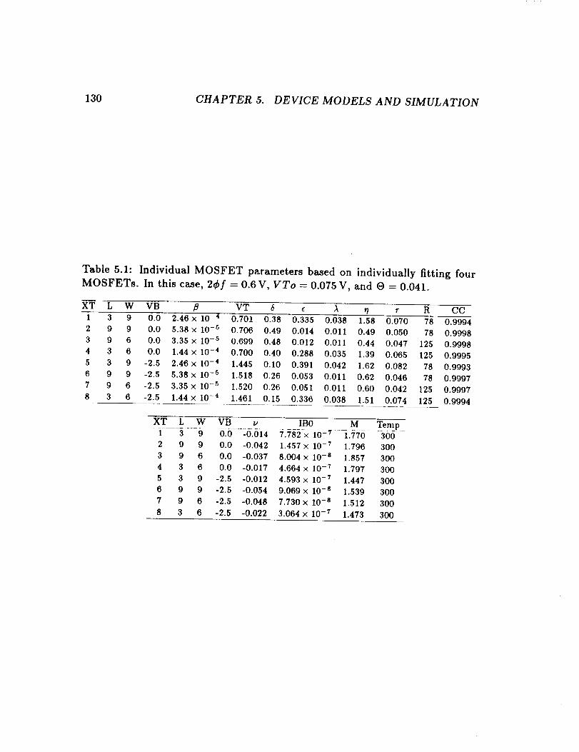
130 CHAPTER 5. DEVICE MODELS AND SIMULATION
Table 5.1: Individual MOSFET parameters based on individually fitting four
MOSFETs. In this case, 2¢f -- 0.6V, VTo = 0.075 V, and O = 0.041.
XT L W VB _ VT 6 e A _ r R CC1 3 9 0.0 2.46 × 10 -4 0.701 0.38 0.335 0.038 1.58 0.070 78 0.9994
2 9 9 0.0 5.38 x 10 -s 0.706 0.49 0.014 0.011 0.49 0.050 78 0.9998
3 9 6 0.0 3.35 x 10 -5 0.699 0.48 0.012 0.011 0.44 0.047 125 0.9998
4 3 6 0.0 1.44 x 10 -4 0.700 0.40 0.288 0.035 1.39 0.065 125 0.9995
5 3 9 -2.5 2.46 × 10 -4 1,445 0.10 0.391 0.042 1.62 0,082 78 0.9993
6 9 9 -2.5 5.38 x 10 -5 1.518 0.26 0.053 0.011 0.62 0.046 78 0.9997
7 9 6 -2.5 3.35 x 10 -5 1.520 0.26 0.051 0.011 0.60 0.042 125 0.9997
8 3 6 -2.5 1.44 x 10 -4 1.461 0.15 0.336 0.038 1.51 0.074 125 0.9994
XT L W VB v IB0 M Temp
2 9 9 0.0 -0.042 1.457 X 10 -7 1.796 300
3 9 6 0.0 -0.037 8.004 x 10 -s 1.857 300
4 3 6 0.0 -0.017 4.664 x 10 -7 1.797 300
5 3 9 -2.5 -0.012 4.593 x 10 -7 1.447 300
6 9 9 -2.5 -0.054 9.069 x 10 -s 1.539 300
7 9 6 -2.5 -0,048 7.730x 10 -s 1.512 300
8 3 6 -2.5 -0.022 3.064 × 10 -7 1.473 300

5.1. MOSFET SUBTHRESHOLD PARAMETER EXTRACTION 131
Table 5.2: Individual MOSFET parameters derived from the global FET pa-
rameters given in Table 5.3. In this case, 2¢f -- 0.6 V and VTo = 0.075 V.
XT L W VB _ VT 6 c A _ r R CC
1 3 9 0.0 2.39 × 10 -4 0.702 0.37 0.338 0.039 1.52 0.067 50 0.9994
2 9 9 0.0 5.39 x 10 -s 0.704 0.48 0.032 0.012 0.54 0.049 50 0.9995
3 9 6 0.0 3.35 x 10 -5 0.700 0.51 0.032 0.010 0.54 0.049 81 0.9980
4 3 6 0.0 1.48 x 10 -4 0.698 0.40 0.338 0.038 1.52 0.067 81 0.9993
5 3 9 -2.5 2.39 x 10 -4 1.449 0.11 0.338 0.039 1.52 0.067 50 0.9990
6 9 9 -2.5 5.39 x 10 -5 1.514 0.22 0.032 0.012 0.54 0.049 50 0.9966
7 9 6 -2.5 3.35 x 10 -5 1.523 0.26 0.032 0.010 0.54 0.049 81 0.9990
8 3 6 -2.5 1.48 x 10 -4 1.457 0.15 0.338 0.038 1.52 0.067 81 0.9980
XT L W VB u IB0 M Temp
1 3 9 0.0 -0.0!4 8.011 x-i_ 1.766 300
2 9 9 0.0 -0.042 1.810 x 10 -7 1.766 300
3 9 6 0.0 -0.037 1.124 x 10 -7 1.766 300
4 3 6 0.0 -0.017 4.974 x 10 -7 1.766 300
5 3 9 -2.5 -0.012 3.524 x 10 -_ 1.487 300
6 9 9 -2.5 -0.054 7.961 x 10 -s 1.487 300
7 9 6 -2.5 -0.048 4.943 x 10 -s 1.487 300
8 3 6 -2.5 -0.022 2.188 x 10 -T 1.487 300

132 CHAPTER 5. DEVICE MODELS AND SIMULATION
Table 5.3: Global MOSFET parameters. The parameters which are indented
are calculated; all other parameters are measured.
Transistor Parameter
BETA:
THRESHOLD:
DELTA:
TAU:
ETA:
EPSILON:
LAMBDA:
M:
IB0:
Value Standard + %
Deviation ±
AW(#m) = 1.086 ± 0.211 (19.38%)
AL(pm) = 1.249 4- 0.071 (5.71%)
VTf0(V) = 0.711 4- 0.028 (3.89%)
Vot(V) : 0.604 4- 0.027 (4.39%)
VTo(V) = 0.077 4- 0.024 (31.35%)
r(vV) = o.8194-o.o18 (2.16%)KLG(V x pm) = 0.005 4- 0.012 (260.24%)KLGB(pm) = 0.057 4- 0.007 (11.77%)
KWG(V x #m) = -0.051 + 0.068 (-134.17%)
KWGB(V x _m) = 0.065 4- 0.039 (59.42%)
D0(v/V) = 0.355 4- 0.022 (6.09%)
KLD(pm) = 0.248 4- 0.039 (15.54%)
KWD(#m) = 0.422 4- 0.138 (32.75%)
o(1/v) : 0.0434- 0.003 (6.25%)KLT(pm/V) = 0.042 4- 0.007 (15.34%)
RW(n ×/zm) = 401.965 4- 62.943 (15.66%)
H0(1/V) = 0.251 4- 0.062 (24.68%)
KiH(pm/V) = 2.227 4- 0.150 (6.72%)
E0(1/V) = 0.057 4- 0.022 (39.38%)
KLE(pm/V) -- 0.690 4- 0.054 (7.83%)
L0(1/V) = 0.006 4- 0.003 (47.28%)
KLL(um/V) = 0.062 4- 0.003 (4.52%)
KWL(_m/V) = 0.020 4- 0.016 (80.63%)
MO(uuitless) = 1.267 4- 0.037 (2.94%)
Vit(V) = 0.080 4- 0.011 (13.94%)
rm(CV) = 0.772 4- 0.075 (9.68%)
ro(_/V) = 7.788 4- 0.424 (5.44%)
File : [SANG.TRY2]C30N61

5.1. MOSFET SUBTHRESHOLD PARAMETER EXTRACTION 133
3211, , ,/t2568
O 1926
1284c_:_:__-
642 IB _
0 I I ] I I
SUBTHRESHOLD I SATURATION
29 I i I u _ t
: dID_" 23 -
_ ,, _u_.-_ _
-_ _-0 I I -0.65 0.69 0.73 0.77 0.81 0.85
UG (V)
Figure 5.7: MOSFET drain characteristics for VDS = 5V. This graph
shows that the slope is continuous at the subthreshold-saturation boundary at
VGS = VT = 0.700V.

134 CHAPTER 5. DEVICE MODELS AND SIMULATION
2209r1767
<_- ,D= ,c+ ,B\ ',_ I
----" 883
0 I i _ I_ I41 --I-- -I_
SUBTHRESHOLD SATURATION LINEAR
14.7 ! , I _ i
I d,D /',- ,, _UG.....J ,Z'-- .! ,, .7/! /
O(-9_1_8,8 ', / /'_ d,c" -t/ / _
=td 5.9 _ { --_ /- ', /_ J , diE}
0,0 I l0.65 0.69 0.73 0.77 0.81 0.85
UG(V)
Figure5.8:MOSFET draincharacteristicsforVDS = 0.05V. This graph shows
that the slope iscontinuous at the subthreshold-saturation and saturation-linear
boundaries.

5.2. INTEGRATED CIRCUIT SIMULATION ON THE HYPERCUBE 135
ID = IB + IC. As seen in Figure 5.7, where VDS = 5 V, the derivatives are
continuous across the subthreshold-saturation boundary at VT = 0.700V. As
seen in Figure 5.8, where VDS = 0.050V, the derivatives are continuous not
only at the subthreshold-saturation boundary but also at the saturation-linear
boundary. This ":hows that the JFETFIT MOSFET model maintains continu-
ity in the derivatives at both the subthreshold-saturation and saturation-linear
boundaries.
5.1.5 Conclusions
Simple expressions are presented for the extraction of the subthreshold current
from MOSFETs. The expressions are derived from a bipolar model of the MOS-
FET operating in the subthreshold region. This region is characterized by the
three parameters: Vit, Fro, and FO. Using the interface trap potential, Vit and
the oxide threshold voltage, VTo, derived from the active region allows the ex-
traction of Vot, the oxide trap potential. An expression suitable for inclusion in
SPICE-like simulations was given and it was shown that the derivatives of this
function are continuous at the threshold voltage. Experimental data indicates
that Fm values are close to F values but F0 values differ significantly from F
values where F is derived from the active region. Thus, Fm values serve as a
double check of F and F0 serves as a subthreshold fitting parameter.
5.2 Integrated Circuit Simulation on the
Hypercube
5.2.1 Objectives
The objectives of this task were:
° To determine the feasibility of transporting the SPICE circuit simulator
(University of California, Berkeley) to the hypercube concurrent comput-
ers being constructed at JPL, rewriting code as necessary, to exploit con-
currency in computation.
° To understand the simulator and its algorithms, to gain insight into the
distribution and decomposition of SPICE onto the JPL computers, and
generally to acquire the expertise required to deal with the problem.

136 CHAPTER 5. DEVICE MODELS AND SIMULATION
3. To begin development of a simulator providing easily incorporated device
models, transistor-level simulation, and a programmable fault environment
(for the introduction of simulated faults) using the SPICE transport as a
starting point.
4. To execute benchmarks upon the new code for both correctness and speed.
The specific goals were:
1. To implement a subset of SPICE able to compute transient analyses for
transistors, resistors, capacitors, and programmable current and voltage
sources.
2. If succeeding in this, to begin to enhance the code with the other features.
5.2.2 Progress and Results
The subset of SPICE (mentioned in Section 5.2.1) has been completely imple-
mented. To achieve this, the decomposition problem has been adequately solved,
and programs written to accept standard SPICE decks, perform load balancing
and communication routings, generate tables for downloading into the hyper-
cube, and format output results for display. These ancillary codes are complete.
The SPICE subset itself, executing on the cube, accepts these tables properly
and is able to produce correct numerical results.
This effort terminated just as the benchmarking of large circuits commenced.
At the end of the effort an unexplained fault caused simulations to "hang"
randomly and, for this reason, no useful timing results could be acquired.
5.2.3 Significance of the Results
The transport of SPICE onto the hypercube was successful. Increase of memory
resources, and identification of the unexplained fault, which is either an unini-
tialized memory error or an intermittent communication failure, should remove
all remaining obstacles. The code has been sufficiently understood, as mani-
fested in part by our modifying of SPICE 3 to execute a new MOSFET model,
and in part by the successful transport to the cube. The decomposition and
exploitation-of-concurrency issues are well understood, and we await only the
appropriate machine resources to commence simulation and timing experiments
on large circuits.

5.2. INTEGRATED CIRCUIT SIMULATION ON THE HYPERCUBE 137
The most important result is that we have learned how to decompose the
problem onto a hypercube of any dimension: the codes already written support
any cube from 32 nodes to 1024 nodes.
The future development of SPICE on the hypercube (by inclusion of a pro-
grammable fault facility) is expected to assist in the modeling of single-event
upsets of Random Access Memories (RAMs). The modeling of the memory re-
sponse to heavy ion hits requires repetitive simulations in order to determine
the upset point (critical charge). SPICE on the hypercube should speed up the
process of both evaluating existing RAMs and designing new RAM cells that
are more resistant to heavy ion upset.
To make this program a viable laboratory utility, the importance of ease
of access between the laboratory's VAX computers (which generate the SPICE
tables) and the hypercube (which executes the tables) cannot be understated.A form of the JPL MARK II batch scheduler and file server for the JPL MARK
III cubes would be highly desirable for this application.
5.2.4 Personnel
We are grateful to the following members of the community at the California
Institute of Technology: Sven Mattison and Charles Seitz (Computer Science)
for foundational work on the problem, Geoffrey Fox and colleagues (Physics) for
their assistance in the decomposition and load-balancing issues, Alain Martin
(Computer Science) for assistance with the resulting intractable optimization
problem, and James Okamoto (Physics) for SPICE code benchmarking.
5.2.5 Publications
The complete report, including computer codes, is being compiled as SPICE ON
THE HYPERCUBE, JPL Internal Report, December 1986.


Chapter 6
A Test Chip Case Study
PRECEDING PAGE BLANK h;OT r,..[,_,F..D
139

140 CHAPTER 6. A TEST CHIP CASE STUDY
6.1 Introduction
This case study is an application of the methodology developed in the Product
Assurance Technology Program for the qualification circuits fabricated at a sil-
icon foundry. The study consists of an analysis of 3-/zm, CMOS/bulk, p-Well,
single metal, single poly wafers from a foundry run for the CRRES Chip project.
The CRRES Chip geometry (CIF) files were submitted to VLSI Technology Inc.
(VTI) for fabrication. Four wafers from Lot Number 4236-0000C4, Run A366
were returned to JPL for testing and qualification, and were code-named "VTI-
2." These wafers were numbered 1 (broken on left), 4, 5, and 10.
Over 110 CRRES chips were fabricated on each wafer in a grid 13 chips wide
at the diameter of the wafer. The wafer is shown in Figures 6.1 and 6.2. The
chips on these wafers are identified by 13 rows and 13 columns, where location
row 1, column 1 is at the lower left-hand corner of the wafer. Each chip is 7130
(horizontal) by 7025 (vertical) micrometers, measured center to center on the
uncut wafers. In wafer number 1, columns 1 and 2 are missing.
Two test vehicles were included on this run: the first, a Test Strip containing
a small number of selected test structures, was placed on each of the CRRES
chips (over 100 sites). The second, a Test Chip of the same area as the CRRES
chip and containing a large number of test structures, was placed in a regular
3 × 3 matrix within the "prime site," i.e., the central section, of each wafer.
Each Test Chip was separated from the others by 3 wafer sites.
The purpose was to compare results obtained from measurements of Test
Strips with those of Test Chips to determine the area required for test structures
on a wafer. It was expected that Test Chips might be adequate to characterize
the wafer for certain parameters but Test Strips, which provide much more wafer
coverage, might be necessary for other parameters.
Section 6.11 contains a full set of wafer maps from wafer #10.
6.2 Areas of Investigation
Each wafer contained over 100 production chips, each bearing a Test Strip. At
the same time there were 9 dedicated Test Chips on each wafer. Among the
issues explored during the preparation of the Test Chips and Strips, and during
the data acquisition and its subsequent analysis, were the following:
1. The first issue was to determine how frequently a parameter needed to be
sampled across a wafer. Comparisons between data from the Test Chips

6.2. AREAS OF INVESTIGATION 141
Figure 6.1: Four-inch diameter silicon wafer from run VTI-2.

142 CHAPTER 6. A TEST CHIP CASE STUDY
/f
i\
__AA A A A AA A X__A>AA A!V2AAA
A A AAAAA
/ X A A C D D C VI E E C A \ CH,PSINCLUDED LOCATION
A A A A A A A A A A A A x _ CRRESCHIP-IKRAM ACRRES CHIP-IK RAM ISPECIAI) B
A A A A A A A A A A A A A I ,PLDROP-,NCM,,,,'STS,02 CKELVIN TAPPED TRANS ISTOR D
A A A C A A C IVl B B C B B ARRAYIN-TYPE)KELVIN TAPPED TRANSISTOR E
ARRAY (P-TYPE _B B B B B B B B B B B B B 400ITYPECHIP (D,E)PAD TEST CHIPS (3} (D)
B B B B B B B B B B B B X / VENDORDROPIN Vl, V2INCOMPLETE DIE X
X B B C D D CVIE E CX
\ XBBBBBBBBB×/
N,. B B B BV2B B B>,./"_X B B B B X.
Figure 6.2: Map of the VTI-2 wafer shown in Figure 6.1 where the different
types of chips are indicated in the key.

6.2. AREAS OF INVESTIGATION 143
and Test Strips for different parameters helped to determine the degree of
wafer coverage required.
, A second issue was whether the nine sites were sufficient to fit a surface
which ce_.¢eyed "sufficient" detail (wafer mapping), and if so, for which
parameters. Therefore, a quantitative comparison was made between the
surface fitted from the many Test Strips and the surface fitted from the
nine Test Chips.
3. The issue of determining which points were statistical outliers, and how
to identify them, was also approached using two different techniques:
(a)
(b)
The first technique was applied to the Test Strip data and involved
two passes over the data: the first pass combined corresponding data
from all wafers to plot global histograms (for this procedure to be ac-
curate, the wafers must be similar enough to be considered samplings
from the same population and no wafer can depart pathologically
from the population). From these global histograms, the criteria for
exclusions (identification and elimination of outliers) for the second
pass were determined. The second pass applied these exclusion win-dows to the individual wafers.
The second exclusion technique was applied to the Test Chip data.
In this case, exclusions were made to data from each wafer inde-
pendently. The resulting distributions were used to create the lot
summary data using no further exclusions. In effect, decisions on
exclusions were made on each wafer in isolation from the others, and
the results were subsequently combined. We were curious to know if
the results would be realistic, and what clues would become manifest
when this method was inadequate. This involved a comparison of the
summary results for the two methods. The reason for seeking the
validity of the latter technique is due to the severe data management
problems of the first technique.
4. The final issue concerned correlations between test structure data and
certain functional circuits on the production chips. Examples of the test
structure data are transistor thresholds, KP, etc., compared with the re-
sults of functional circuits such as a RAM or the timing sampler described
elsewhere (Chapter 7) in this report.

144 CHAPTER 6. A TEST CHIP CASE STUDY
6.3 Test Chip and Test Strip Design
As used in this report, the nine Test Chips are chips fully dedicated to test
structures; therefore, only a few Test Chips can be included on a production
wafer. The Test Chips on this run consumed about 8 percent of the available
chip positions, and occupied nine "prime sites" on the wafer.
Test Strips have much smaller dimensions than Test Chips, limiting the num-
ber of test structures that can be placed on each strip. However, the Test Strip
is replicated on every site on the wafer that contains a production chip. In
this run, the Test Strip consumes approximately 5 percent of the area of the
production chip and thus about 5 percent of the total area of the wafer.
Test structures for the Test Chips were selected from the following categories:
1. Process parameter extraction.
2. Device parameter extraction.
3. Circuit parameter extraction.
4. Layout rule checking.
5. Yield analysis.
The size of the Test Chip allows structures from all categories to be included;
the smaller size of the Test Strip allows selected structures from only the first
three categories to be included.
To satisfy the requirements of parameter extraction routines for circuit sim-
ulators, transistors of various sizes are included on the Test Chips. Dimensions
for both n- and p-channel transistors included on this run, along with the cal-
culated KP for each size, are shown in Table 6.1. These values were derived
from the maximum slope,/3, of the ID versus VG curve for VD = 50 mV us-
ing KP = /3L/W where L and W are the as-drawn channel length and width
dimensions, respectively. The KP values shown in Table 6.1 are not corrected
for AL and AW.
6.4 Geometry and Test Program Generation
Once the decisions on the contents of the Test Chip and the Test Strip had been
made, the JPL Test Chip Assembler (TCA) was used to generate the geometry.
The Test Chips were identified as CM5111, and the Test Strips as ST5102. The

6.4. GEOMETRY AND TEST PROGRAM GENERATION 145
Table 6.1: Transistor Geometries for both n- and p-channel transistors from Run
VTI-2, 3-#m CMOS/Bulk p-well, W vs. L, showing KP in #A/V 2 (mean + a
at VBS = 0) for each Device. The data shown is from wafers 1, 4, 5, and 10.
n-Channel 15.0
Transistors
As-Drawn
Width
(#m)
p-Channel
Transistors
As-Drawn
Width
(#m)
12.0
9.0
6.0
4.5
3.0
15.0
12.0
4.5
3.0
As-Drawn Length (#m)
2.0 3.0 6.0 9.0 12.0 15.0
56.7 49.0 46.5 45.2 44.7
-t-2.7 +1.5 =t=1.4 =t::l.1 =t:0.8
55.7
+3.3
103. 54.6 44.5
=}=12. +3.5 +0.9
49.9 44.4
±3.4 ±I.I
81.7 47.6 43.8 41.6 40.6
±9.2 ±3.3 ±1.3 ±1.3 ±1.3
77.2 44.6 38.4
=t=8.7 +2.6 +1.9
-.688
±.029
-.717
=t:.026
-.809 -.827
±.027 =1=.018
- .807
:1:.023
-.811
± .025
- .829
±.021
-.836 -.860
±.020 ±.019
-.854
-{-.021
-.831 -.837 -.836
±.017 =t=.022 +.024
- .846 - .844
±.023 ±.017
- .858
±.019
- .866 - .872
±.019 ±.016
- .888
±.017

146 CHAPTER 6. A TEST CHIP CASE STUDY
two projects were laid out independently. Using a text input file containing gross-
level specifications of the required structures and placement, the TCA generated
all detailed geometry automatically. The result was an output file in Caltech
Intermediate Form (CIF) which was sent directly to the foundry for fabrication
(in the case of the Test Chip CM5111), or else merged into the geometry for the
CRRES Chip project (in the case of the Test Strip ST5102).
In addition to producing geometry files in CIF, the TCA produced descrip-
tion files which state the exact locations of the structures in the project, the
type of structure, and the essential parameters of each structure. These files
were routed to the Test Program Generator, which automatically prepared a
test program to be executed by the prober and the test instrumentation. The
compilation of a test program on a VAX 11/780 takes about ten minutes. Two
separate wafer probing programs were generated: one to test the Test Strips
and one to test the Test Chips.
6.5 Wafer Probing and Disposition of Data
The VTI-2 wafers were probed using JPL's test system which, at the time, was
built around an LSI-11 computer. Since this system has been replaced by a
microVAX-II system, no machine-dependent details of the test software will be
given. The test system was designed to execute test programs generated for it
following the steps outlined above. Thus, the electrical test and the position of
the wafer prober were automatically programmed by the earlier steps.
This study used four wafers, numbered 1, 4, 5, and 10. Wafer 1 had the
leftmost two columns (of the 13 x 13 grid) missing.
The output from the wafer probing was a binary, sequential file which was
moved to a VAX 11/780 computer for final formatting. On the VAX, the file
was processed by a program called the Test Data Preprocessor, to organize the
raw data into labeled, archival, data files. Once this is complete, the binary fileis discarded.
The result is a series of small ASCII files written in a format called CRUNCH
reference files. Each CRUNCH file, which contains all data from all chips for
one particular structure, has an identifier incorporated into its name which is
uniquely assigned to this structure by the Test Compiler. For example, had
there been a transistor (of given dimensions), called "349" by the test compiler,
drawn into the Test Chip, then one CRUNCH file for each wafer would have
been generated, each with the characters "349" as part of its filename. Since
the Test Chip appears nine times on each wafer, then one such CRUNCH file

6.6. TEST STRIP WAFER MAP PRELIMINARY RESULTS 147
would contain nine points. Each of the nine points is labeled in such a way that
the exact coordinates of each site, on the wafer, are known. Thus, one CRUNCH
file contains enough data to fit a surface for a wafer map.
The test data preprocessor, furthermore, labels the data in each CRUNCH
file with informution it obtains from the "description file" output of the TCA.
Therefore, the labeling of the output data, and the construction of the CRUNCH
files, is fully automatic.
Each CRUNCH filename incorporates information to identify the wafer num-
ber and whether it was taken from the Test Strip or Test Chip. This filename
structure allowed algorithmic file construction and automated access to files.
This is essential to automating the analysis of the (formatted but as-measured)
data in the CRUNCH files, by the main analysis tool, a program called STMJPL
which was derived from the National Bureau of Standards statistical analysis
program STATII [31].
6.6 Test Strip Wafer Map Preliminary Results
The STMJPL program generates wafer maps of the important parameters and
structures on the Test Strips. The exclusions applied to the data were deter-
mined by studying the global histograms to decide which points would be con-
sidered "outliers." In this case, the histogram data was normally distributed,
indicating to a first approximation that no one wafer was significantly different
from the others. Two histograms from this run are shown: the first is the dis-
tribution of contact resistance for metal to n+poly (Table 6.2), an example of
normally distributed data, and the second is the sheet resistance of the metal
layer (Table 6.3), showing a skewed distribution. Wafer maps were generated
for individual wafers. A map of contact resistance to n+poly is shown, once in
"full" mode (Table 6.4) and the second time in "avenue" mode (Table 6.5).
6.7 Parametric Test Structure Probing: Initial
Qualitative Results Test Strip ST5102
From the entire series of wafer maps and the statistics printed with each plot,
a preliminary summary was prepared. This is not the result of a full statistical
analysis on the data, but rather a tabulation of information obtained from the
wafer maps. The data referred to in this section is listed in Table 6.6.
1. Sheet Resistance from Split-Cross-Bridge Resistors:

148 CHAPTER 6. A TEST CHIP CASE STUDY
Table 6.2: Histogram of the normal distribution of contact resistance for metal
to n+poly on the Test Strips of Run VTI2, Wafer #1. Mean -- 2.1112;
Stdev -- 0.4312; % Stdev -- 20.69; Median -- 2.1512; Minimum = 0.7312;
Maximum -- 3.23 12.
INTERVAL NO.
MIDPOINT OBS. NUMBER OF OBSERVATIONS
(OHMS) 0 10 20 30 4O
INCLUDED = 418; EXCLUDED = 0
LOWER BOUND -- 0.73; UPPER BOUND -- 3.23; BIN COUNT = 34
POINTS BELOW BIN 1 = 0; POINTS ABOVE BIN 34 = 0; BIN WIDTH = 0.0738

6.7. PARAMETRIC TEST STRIP PROBING 149
Table 6.3: Histogram of the skewed distribution of sheet resistance of the
metal layer from the Split-Cross-Bridge Resistor on the Test Strips of Run
VTI2, Wafer #l. Mean = 0.033[1/D; Stdev = 10-sial/D; % Stdev = 3.15;
Median = 0.0316Vt/[] ; Minimum = 0.0305fl/[] ; Maximum = 0.0357fl/_.
INTERVAL NO. NUMBER OF OBSERVATIONS
MIDPOINT OBS.
(RSHEET) 0 10 20 30 4O
0.0306 3 ***
0.0307 9 ******
0.0309 18 ******
0.0310 34 ******
0.0312 41 ******
0.0314 39 ******
0.0315 47 ******
0.0317 43 ******
0.0318 31 ******
0.0320 > 23 ******
0.0321 17 *****************
0.0323 8 ********
0.0324 7 *******
0.0326 11 ***********
0.0328 2 **
0.0329 + 9 *********
0.0331 9 *********
0.0332 9 *********
0.0334 4 ****
0.0335 9 *********
0.0337 3 ***
0.0339 6 ******
0.0340 3 ***
0.0342 5 *****
0.0343 4 ****
0.0345 4 ****
0.0346 1 *
0.0348 0
0.0349 4 ****
0.0351 0
0.0353 2 **
0.0354 0
0.0356 1 *
0.0357 2 **
LOWER BOUND = 0.0305; UPPER BOUND = 0.0358; BIN COUNT = 34POINTS BELOW BIN 1 = 0; POINTS ABOVE BIN 34 = 0; BIN WIDTH = 1.56 x 10⁻⁴

150 CHAPTER 6. A TEST CHIP CASE STUDY
Table 6.4: "Full" Wafer Map of Contact Resistance to n+Poly Wafer #1.
Mean = 2.40_, Stdev = 0.31811, % Stdev = 13.3, Median = 2.36_,
Minimum = 1.69 12, Maximum = 3.24 12.
VT-i260866:c,6i cMos VTi2: _VTI DE_]._i236-0000C4 RUN A366 3U CMOS/BULK
(VTI2)( t)(ST5102)860,870,880,0
21-JUN-1986 22:56:18.00- ST5102: TEST STRIP CONTACT RESISTOR
INCLUDED= 95 EXCLUDED-- 0 NON-POINTS= 13 N= 1.00
13 v
12 v
11 v
10 v
9 v
8 v
7 v
6 v
5 v
4 v
3 v
2 v
1
)< )< >< )( )( )< >< >< )( )( >< ><
78998887776668899
87#77#88#87#76#67#77653
++8756677888877666666554332
++#87#56#78#88777#66#65#44322
+988887777788888777777665544333
+988#88#88#88#88#88#88#76#55#5556
+++99888899899988888877765666555566
++9988#87789999999888875545666666#666
123455666767888999888776544566666655555
-123455#66#67#77#77#77#76#56#66#65#5555
455566667777666666666666777665666555544
2345566#77#76#55#55#56#67#76#56#55#44#4
.... 13456676655555545666777655555555443
---0134#66666#56#55556677#66#54455#44#3
887777777787655777666666655555433454433
+++9987#77#76#56#77#66#66#55#54#45#44#3
+++988877666655667777656666665545555433
9988877#65#55#56#67#76#56#76#65#55#4332
5556666665556666678875567777765554332
55666#67766778876777667778876544332
666677787778888777777777777544332
666#77#77#78#88#77#66#66#65#432
66666667778888888875555655443
6#66#66#67#88888#76#55#5554
55544556666666556555555
33#44#55#55#55#55
>< >< >< >< >( >< >< >< >< >< >< ><
1 3 5 7 9 11 13
2 4 6 8 10 12
-: less than 0,73
0:0.73 to 0.98
1:0.98 to 1.23
2:1.23 to 1.48
3:1.48 to 1.73
4:1.73 to 1.99
5:1.99 to 2.24
6:2.24 to 2.49
7:2.49 to 2.74
8:2.74 to 2.99
9:2.99 to 3,24
+: 3.24 or greater

6.7. PARAMETRIC TEST STRIP PROBING 151
Table 6.5: "Avenue" Wafer Map of contact resistance to n+Poly for Wafer
#1. Mean = 2.4012, Stdev -- 0.318f_, % Stdev -- 13.3i2, Median = 2.36f_,
Minimum = 1.6.o fl, Maximum -- 3.24 _t.
VTI200860.C01 CMOS VTI2: VTI DEV.4236-0000C4 RUN A366 3U CMOS/BULK
(VTI2)( 1)(ST5102)860,870,880,0
21-JUN-1986 22:56:18.00 - ST5102: TEST STRIP - CONTACT RESISTOR
Array = OHMS CP C n+POLY 3.00000
13
12
11
10
9
8
7
6
5
4
3
2
1
INCLUDED= 95 EXCLUDED= 0 NON-POINTS= 13 N= 1.00
>< >< >< >< >< >< >< >< >< >< >< ><
.8..888...66688..
v 8 .... 88888...666 .... 6..
..8..66..8888..666666..4..2
v ...8.6.66.8888...66666..44.22
..8888 ..... 88888 ...... 66..44...
v ..88888888.888888888888.66 ...... 6
..... 8888..8...888888...6.666 .... 66
v .... 8888..8 ....... 8888...4.666666.666
.2.4..666.6.888...888..6.44.666666 .....
v ..2.4..66666 ............ 6..666666 ......
4...6666 .... 666666666666...66.666 .... 44
v 2.4..666..8.6 ........ 666...6..66...4444
...... 4.66.66 ...... 4.666...6 ........ 44.
v ...0..4.66666..66 .... 66...66..44...444.
88 ........ 8.6 ..... 6666666 ..... 4..4,44..
v ..... 8 ...... 6..6.,.666666 ..... 444..44..
.... 888..6666,.66 .... 6.666666..4 .... 4..
v ..888,..6 ...... 666.8.6..6..666 ..... 4..2
...666666...66666.88...6 ..... 6...4..2
v ..66666..66..88.6...66...88.6.44..2
6666...8...8888 ............. 44..2
v 6666 ....... 8888 .... 6666666.44.2
6666666...88888888 ..... 6..44,
v 666666666..88888..6 ....... 4
...44..6666666..6 ......
...44 ...... 4 .....
>< >< >< >< >< >< >< >< >< >< >< ><
1 3 5 7 9 11 13
2 4 6 8 10 12
-: less than 0.73
0:0.73 to 0.98
1:0.98 to 1.23
2:1.23 to 1.48
3:1.48 to 1.73
4:1.73 to 1.99
5:1.99 to 2.24
6:2.24 to 2.49
7:2.49 to 2.74
8:2.74 to 2.99
9:2.99 to 3.24
+: 3.24 or greater

152 CHAPTER 6. A TEST CHIP CASE STUDY
(a) R_p,mer (p+diffusion): Combining all points (415) from all wafers, the
mean is 87.2 =L 1.9 _l/V1. Individual wafer statistics match combined
statistics very closely. On all wafers the sheet resistance increased
linearly from the bottom to the top of the wafer.
(b) Rsn,pOLY (n+poly): Combining all points (419) from all wafers, the
mean is 22.5 + 0.67 fl/[]. Individual wafer statistics match combined
statistics very closely; only wafer #5 shows slightly higher (0.2 fl/[])
sheet resistance overall. All wafer maps show uniform sheet resistance
except on the periphery of the wafer, where, for a very short distance
(1 to 2 chips) from the edges, higher sheet resistance is found. In
column 13 it is about 212/_ higher than on the rest of the wafer.
(c) R,n.D_F_" (n+diffusion): First, it should be noted that the n+diffusion
layer showed a bimodal distribution in sheet resistance. For all four
wafers, row 13 had sheet resistance greater than the rest of the wafer
by 20 - 25 fl/[3. The effect is very abrupt, affecting all chips on only
that row. Therefore, the top row was excluded from the analysis and
contains chips that probably should not be used. A corresponding
effect also appeared in the n-channel transistor and the inverter maps;
all n-channel transistors and inverters on the top row were excluded
as outliers. Combining all points (395) from all wafers, the mean
is 21.8 + 1.312/D. The distribution is skewed downwards, that is,
the "tail" is toward low resistance values. The mode appears to be
at about 2312. Individual wafers have statistics which match the
combined statistics very closely, with no wafer-to-wafer shifts, and
the skewed behavior appearing in all four wafers. The wafer maps all
show fairly uniform sheet resistance except on the periphery of the
wafer. On all four wafers there is a crescent-shaped region centered
to the right along the periphery where the resistance is lower than
on the rest of tile wafer. The crescent at its thickest is about 2 chips
distance across. The effect appears on all four wafers. The area not
part of the crescent, which is a circular area within the crescent with
its center point to the left of the wafer center, has very uniform sheet
resistance at the mode value (approx. 23 _/[]).
(d) R_,METAL (Metal): Combining all points (408), from all wafers, the
mean is 0.0320 =t=0.0010 l-l/[3. The distribution is skewed upwards,
that is, the "tail" is toward high resistance values. The mode appears
to be at about 0.0315 i'l/[3. Statistics from individual wafers match
the combined statistics very closely, the skewed behavior appearing

6.7. PARAMETRIC TEST STRIP PROBING 153
in all four wafers. All four wafer maps show fairly uniform sheet
resistance except on the periphery of the wafer, where higher sheet
resistance is found. The area of higher resistance is an annulus about
1 chip across.
2. Contact resistance:
(a) Rcmn,POLY (Metal to n+poly): Combining all points (418) from all
wafers, the mean value is 2.12 :t: 0.44 fl. The distribution is normal.
Individual wafers have similar statistics, with wafer # 1 slightly higher
(mean about 2.38 _) and wafer #4 slightly lower (mean about 1.72 f_).There was no common trend in the individual wafer maps except for
a pattern of the rightmost side of each wafer, one or two chips wide,
having the lower contact resistances on each wafer.
(b) Rcmp,DIFF (Metal to p+diffusion): Combining all points (399) from all
wafers, the mean value is 15.0 + 3.4 I2. The distribution is normal.
Individual wafers have similar statistics, with wafer # 1 slightly higher
(mean about 16.6 I2) and wafer #4 slightly lower (mean about 13.2 f_).
This follows the pattern for metal-n+poly contacts stated above. All
four wafers showed the common trend of having the lowest contact
resistances on the right side of the wafer, and increasing linearly as
one moves left across the wafer. The effect is much more prominent
than for the metal to n+poly contacts listed above.
(c) Rcmn.DIFF (Metal to n+diffusion): Combining all points (392) from all
wafers, the mean value is 5.13 ± 1.312. The distribution is normal.
Individual wafers have similar statistics, with wafer #4 lower (mean
about 4.78 fI). All four wafers showed the common trend of having the
lowest contact resistances on the right side of the wafer, in a crescent
pattern the width of two chips at its thickest point. The remaining
circular region (with its center left of wafer center) has, within itself,
resistances going linearly from intermediate to high values as one
moves across that circular region from right to left.
(d) General comments on all contact wafer maps: The surfaces were con-
sistently irregular, except for the overall trends noted above. High
values tended to form a mesh of ridges while relatively lower values
formed valleys. As seen from the standard deviation figures above,
the difference in resistance moving from a ridge into a valley could
be several ohms. Valleys were about three or four chips in diameter.

154 CHAPTER 6. A TEST CHIP CASE STUDY
Table 6.6: Test Strip ST5102 results. Parametric data was taken from four 4-inch
diameter CMOS/bulk wafers each containing 108 Test Strips and 9 drop-in Test
Chips. The parameters from the Test Strips and Test Chips were fitted to
over 3700 pixels and compared pixel by pixel to compute the parameter percent
difference using 100 × (Chip - Strip)/(Strip). The data mean and standard
deviations were computed after outlier exclusion.
DATA KEY: (# STRIPS VS # CHIPS)
(MEAN %DIF +- ST DEV. %DIF)
(STRIP MEAN +- STRIP STDEV)
(CHIP MEAN +- CHIP STDEV)
lEST STRUCTUREPARAMETER WAFER 1 WAFER 4 WAFER 5 WAFER I0 LOT SUMMARY..............................................................................................................
BRIDGE R 89 vs 8 102 vs 7 I02 vs 7 102 vs 8 395 vs 30SHEET R 3.69 +- 7.52 4.01 +- 6.92 3.4l +- 7.03 4.26 +- 6.79 NOT APPLICABLE
Rsn DIFF 21,8 +- 1.40 21.8 +- 1.31 21.9 +- 1.32 21.9 +- 1.36 21.8 +- 1.34
(ohm/sq} 22.5 +- 0.80 22,5 +- 0.81 22.4 +- 0.79 22.5 +- 0.75 22.5 + 0.75
BRIDGE R 89 vs 7 101 vs 6 102 vs 6 ]02 vs I 394 vs 26
LINEWIDTH -0.34 +- 1,87 -0.42 +- 1.34 -0.24 +- 1.76 -0.80 +- 1.80 NOT APPLICABLE
Wn DIFF 4.59 +- O.Ol 4.78 +- 0.08 4.60 +- 0.05 4.58 ÷- 0.05 4,64 +- 0. II
(urn) 4.57 +- 0,04 4.78 +- 0.05 4,60 +- 0.02 4.56 +- 0.02 4.62 +- 0.09
BRIDGE R 94 vs 8 I07 vs 7 107 vs 8 107 vs 8 4IS vs 31
SHEET R -0.38 +- 0.69 -0.10 +- I.O0 -0.91 +- 1.64 -0.40 +- 0.81 NOT APPLICABLE
Rsp DIFF 87.3 +- 1.91 86.9 +- 1.86 87.2 +- 1.87 87.2 +- 2.02 87.2 +- ].92
(ohm/sq) 86.7 +- ].49 86.6 +- 1.68 86.1 +- 2.18 86.7 +- 1.52 86.6 +- 1.67
BRIDGE R 94 vs 7 104 vs 7 107 vs 5 107 vs 8 412 vs 27
LINEWIDTH -0.25 +- 1.76 -0.67 +- 2.52 0.05 +- 2.]6 -1.20 +- 1.97 NOT APPLICABLE
Wp DIFF 4.33 +- O.lO 4.49 +- 0.09 4.31 +- O.Ol 4.28 +- 0.08 4.35 +- 0,12
(urn) 4.31 +- 0.03 4.47 +- 0.04 4.30 +- 0.03 4.23 + 0.03 4.33 +- O.lO
BRIDGE R 95 vs 8 108 vs 7 108 vs 7 108 vs 9 419 vs 31
SHEET R -0.74 +- 6.41 1.08 +- 2.93 0.72 +- 3.32 -2.07 +- 3.52 NO1 APPLICABLE
Rsn POLY 22.3 +- 0.68 22.5 +- 0.69 22.8 +- 0.65 22,4 +- 0.06 22.5 +- 0.67
(ohm/sq) 22.0 +- 0.36 22.4 +- 0.78 22.7 +- 0.60 21.8 +- O.SS 22.2 +- 0.65
BRIDGE R 94 vs 6 I07 vs 7 108 vs 6 108 vs 7 416 vs 26
LINEWIDTH 4,73 +- ]9.9 4.17 +- S.14 4.86 +- 6.43 1.4l +- 4.22 NOT APPLICABLE
Wn POLY 2.62 +- 0.17 2.54 +- 0.11 2.54 +- 0.10 2.63 +- 0.10 2.59 +- 0.18
(urn) 2.68 +- 0.06 2.60 +- 0.10 2.63 +- 0.05 2.65 +- 0.08 2.64 +- 0.08
BRIDGE R 95 vs 8 97 vs 7 108 vs 7 108 vs 8 408 vs 30
SHEET R -1.77 +- 3.70 -2.37 +- 4.10 -2.88 +- 3.59 -2.68 +- 4.03 NOT APPLICABLE
Rs METAL 31.9 +- 1,05 31,9 +- 1.08 32.0 +- 1.00 32.0 +- 1.00 31.9 +- 1.01
(mohm/sq) 31.6 +- l.O0 31.4 +- 1.00 31.3 +- 1.00 31.5 +- 1.00 3l.S +- 1.00
BRIDGE R 94 vs 7 97 vs 7 108 vs 6 108 vs 7 407 vs 27LINEWIDTH -0.64 +- 2.58 -2.28 +- 3.]3 -I.17 +- 3.28 -1.96 +- 3,47 NOT APPLICABLE
W METAL 3.79 +- 0.15 3,72 +- 0.13 3.75 +- 0.12 3.87 +- 0.19 3.78 +- 0.16
(urn) 3.73 +- 0.10 3.64 +- 0.10 3.68 +- O.IS 3.80 +- 0.15 3.71 +- 0.14
CONTACT R 89 vs 9 99 vs 8 102 vs 9 102 vs 9 392 vs 35
CONTACT R 5.46 +- 26.6 13.1 +- 31.0 13.5 +- 30.3 IS.6 +- 43.9 NOT APPLICABLE
Rcmn DIFF 5.30 +- 1.12 4.78 +- 1.19 5.24 +- 1.19 5.19 +- 1.43 5.13 +- 1.25
(ohm) 5.67 +- 1.25 4.94 +- 1.26 5.27 +- 1.03 5.41 +- 1.44 5.33 +- 1.22

6.7. PARAMETRIC TEST STRIP PROBING 155
Table 6.6: Test Strip ST5102 results (Continued).
TEST STRUCTURE
PARAMETER WAFER 1 WAFER 4 WAFER 5 WAFER 10 LOT SUMMARY.................................................................................................................
CONTACT R 94 vs 8 91 vs 8 I07 vs 8 107 vs 9 399 vs 33
CONTACT R -0.97 ÷- 14.7 -0.91 +- 14.9 0.41 +- 9.76 0.78 +- 16.4 NOT APPLICABLE
Rcmp DIFF ]6.7 +- 3.41 13.2 +- 3.03 15.2 +- 2.59 14.8 +- 3.74 15.0 +- 3.42
(ohm) 16.4 +- 3.16 12.7 +- 2.71 15.0 +- 2.83 14.0 +- 3.49 14.5 +- 3.24
CONTACT R 95 vs 7 I07 vs 9 ]08 vs g 108 vs 9 418 vs 34
CONTACT R -4.16 +- 13.9 6.14 +- 31.0 15.3 +- 23.4 7.35 +- 18.0 NOT APPLICABLE
Rcmn POLY 2.40 +- 0.32 1.73 +- 0.41 Z.16 +- 0.28 2.22 ÷- 0.43 2.12 +- 0.44
(ohm) 2.31 +- 0.32 1.70 +- 0.34 2.27 +- 0.26 2.25 +- 0.42 2.12 +- 0.42
N-MOSFET 89 vs 8 102 vs 8 102 vs 9 102 vs 9 395 vs 34
THRESHOLD -1.18 +- 1.59 -0.60 +- 1.18 -.094 +- 2.51 -0.41 +- 1.61 NOT APPLICABLE
VTOn 0.674 +- 0.008 0.655 +- 0.012 0.668 +- 0.013 0.680 +- 0.009 0.669 +- 0.014
(V) 0.670 +- 0.011 0.653 +- 0.007 0.670 +- 0.008 0,678 ÷- .007 0.6_ +- 0.012
N-MOSFET 89 vs 8 102 vs 8 102 vs 9 102 vs g 395 vs 34
CONDUCTANCE 1.36 +- 5.06 -0.05 +- 6.41 -2.52 +- 6.82 ].61 +- 5.52 NOT APPLICABLE
KPn-uCo 53.2 +- 2.43 58.0 +- 3.38 55.6 +- 3.39 52.9 +- 2.83 55.0 +- 3.68
(uA/V^2) 53.5 +- 1.93 57.2 +- 4.06 54.0 +- 3,33 53.8 +- 3.49 54.6 +- 3.48
P-MOSFET 94 vs 8 108 vs 9 ]07 vs 9 108 vs 9 4]3 vs 35
THRESHOLD 1.50 +- 1.45 0.91 +- 2.34 -3.55 +- 4.62 0.87 +- 1.49 NOT APPLICABLE
VTOp -0.801 +- 0.010 -0.832 +- 0.016 -0.807 +- 0.011 -0.810 +- 0.012 -0.813 +- 0.017(V) -0.786 +- 0.005 -0,827 +- 0.024 -0.822 +- 0.028 -0.805 +- 0.015 -0.81l +- 0.025
P-MOSFET 94 vs 8 108 vs 9 107 vs 9 ]08 vs 9 413 vs 35CONDUCTANCE -1.60 +- 3.80 3.38 +- 6.05 2.19 +- 4.91 -0.34 +- 5.75 NOT APPLICABLE
KPp-uCo 20.0 +- .860 20.6 +- 1.17 19.8 +- .669 ]9.5 +- 1.20 20.0 +- 1.07
(uA/V^2) 19.8 +- .645 2].I +- .715 20.2 +- .851 19.5 +- .660 20.] +- .944
INVERTER 88 vs 9 102 vs 9 102 vs 9 102 vs 9 394 vs 36
THRESHOLD -2.08"+- 0.68 -1.90 +- 0,84 -2.49 +- 0.95 -2.33 +- 0.88 NOT APPLICABLE
VINV 2.21 +- 0.014 2.17 +- 0.015 2.20 +- 0.011 2.19 +- 0.0]3 2.19 +- 0.022
(V) 2.17 +- 0.015 2.12 +- 0.010 2.15 +- 0.017 2.14 +- O.OOB 2.15 +- 0,020
INVERTER 88 vs 9 102 vs 9 102 vs 9 102 vs 9 394 vs 36
GAIN -].30 +- 5,]1 -0.13 +- 4.34 -3.12 +- 6.01 -2.]9 +- 5.04 NOT APPLICABLE
(unitless) -15.0 +- 0.59 -14.8 +- 0.79 -14.6 +- 0.67 -15.7 +- 0.7] -15.0 +- 0.82-15.3 +- 0.37 -14.9 +- 0.46 -14.9 +- 0.33 -]5.9 +- 0.80 -15.2 +- 0.64
Transistor dimensions: Length - 3 um, Width - 9 um for both n- and p- channel.
Inverter Dimensions: Ln - 3.0, Wn - 4.5, Lp - 3.0, Wp = 6.0 (um, strips).
Ln - 3.0, Wn - 4.5, Lp = 3.0, Wp = 5.6 (um, chips).Contact Dimensions: 3.0 um square, all layers.

156 CHAPTER 6. A TEST CHIP CASE STUDY
This was manifest for all layers. The surfaces were never smooth or
continuous, nevertheless the irregularities were not so closely spaced
that the fitting algorithm could be suspected of working at too fine a
resolution. Again, the features were three to four chips in diameter,
so the fitted surfaces (using roughly a hundred points) were received
with justifiable confidence.
3. Transistors: The following tables contain values for the threshold voltage,
VTO, and KP derived from the maximum slope of the ID versus VG
curve measured at VD = 50 mV. The KP values were calculated using
the as-drawn channel width and length dimensions.
(a) Threshold voltage, VTO (V) at VBS = 0:
Transistor
Dimensions
(#m)n'channei
length=3width=6
n-channel
length=3
width=9
n-channel
length=9width=6
n-channel
length=9
width=9
p-channel
length=3
width=6
p-channel
length=3
width=9
All Wafers Wafer Wafer Wafer Wafer
Combined # 1 # 4 # 5 # 10
0.669 0.674 0.-6-55-- 0.6(_8 - 0.680
:kO.O14 ±0.008 ±0.012 i0.013 ±0.009
395 pts. 89 pts. 102 pts. 102 pts. 102 pts.
0.672 0.676 0.658 0.669 0.683
+0.015 ±0.009 ±0.015 -1-0.013 ±0.009
394 pts. 89 pts. 101 pts. 102 pts. 102 pts.
0.709 0.713 0.696 0.709 0.719
i0.012 ±0.006 _:0.011 ±0.010 ±0.007
394 pts. 89 pts. 102 pts. 101 pts. 102 pts.
0.685 0.688 0.673 0.684 0.693
±0.012 ±0.007 ±0.009 ±0.011 +0.008
391 pts. 89 pts. 99 pts. 101 pts. 102 pts.
-.835 -.821 -.849 -.833 -.834
±0.016 ±0.012 ±0.013 ±0.011 ±0.012
415 pts. 94 pts. 107 pts. 107 pts. 107 pts.
-.813 -.801 -.832 -.807 -.809
±0.017 ±0.010 ±0.016 +0.011 ±0.012
413 pts. 94 pts. 106 pts. 107 pts. 106 pts.

6.7. PARAMETRIC TEST STRIP PROBING 157
Transistor All Wafers
Dimensions Combined
(#m)
p-channel -.860
length=9 +0.014
width=6 414 pts.
Wafer Wafer Wafer Wafer
#1 #4 #5 #10
.845 -.8 5 -.860 :,856±0.008 -t-0.011 ±0.011 ±0.009
94 pts. 106 pts. 107 pts. 107 pts.
p-channel -.846 -.833 -.861 -.845 -.845
length=9 ±0.013 +0.009 +0.011 t0.009 +0.009
width=9 414 pts. 94 pts. 106 pts. 107 pts. 107 pts.
(b) KP = #oCo at VBS --- O. Figures shown are KP (#A/V'):
Transistor All Wafers Wafer Wafer Wafer Wafer
Dimensions Combined # 1 # 4 # 5 # 10
(_m)
n-channel 50.1 48.5 53.4 50.6 47.8
length=3 +3.64 :k2.19 ±3.33 ±3.27 +2.53
width=6 394 pts. 89 pts. 101 pts. 102 pts. 102 pts.
n-channel
length=3
width=9
55.0 53.2 58.0 55.6 52.9
±3.68 ±2.43 -4-3.38 +3.39 ±2.83
395 pts. 89 pts. 102 pts. 102 pts. 102 pts.
n-channel
length=9
width=6
44.6 44.0 46.5 44.2 43.7
±1.51 ±0.74 +0.93 ±1.29 ±0.88
394 pts. 89 pts. 102 pts. 101 pts. 102 pts.
n-channel
length=9width=9
44.6 44.0 46.0 44.3 43.6
±1.24 ±0.66 +0.72 ±1.29 ±0.84
391 pts. 89 pts. 99 pts. 101 pts. 102 pts.
p-channel
length=3width=6
19.2 19.2 20.0 19.1 18.6
±1.06 +0.62 ±1.06 ±0.76 ±1.12
415 pts. 94 pts. 107 pts. 107 pts. 107 pts.
p-channel 20.0
length=3 ±1.07
width=9 413 pts.
20.0 20.6 19.8 19.3
t0.86 ±1.17 ±0.67 ±1.20
94 pts. 106 pts. 107 pts. 106 pts.

158 CHAPTER 6. A TEST CHIP CASE STUDY
Transistor All Wafers Wafer
Dimensions Combined # 1
(#m)
p-channel i5.5 -- 15.7
length=9 +0.54 -t-0.30
width=6 414 pts. 94 pts.
Wafer Wafer Wafer
#4 #5 #10
i6.0 i510 15.3
4-0.26 4-0.43 _=0.52
106 pts. 107 pts. 107 pts.
p-channel 16.3 16.5 16.5 15.9 16.2
length=9 +0.45 +0.23 4-0.30 +0.37 +0.52
width=9 414 pts. 94 pts. 106 pts. 107 pts. 107 pts.
(c) General Comments about Transistor Maps: VTO values were very
uniformly distributed over all wafers with the standard deviation
ranging from 12 - 17mV. KP values for L = 3 #m show more
variability than for L = 9 #m. This is due in part to variations in
the channel length.
4. Inverters ( Pulldown L = 3, W = 4.5; Pullup L = 3, W = 6 ):
(a) VINV (VDD = 5V): After all final exclusions, the mean value is
2.192 4- 0.022 V. The distributions were quite uniform over all four
wafers (394 points). There was a slight tendency for the distribution
to be lower at the perimeter (1 chip from the edge) with this effect
most pronounced for wafer #5.
(b) Gain: With all final exclusions, the mean value is -15.01 =[=0.82
(394 points). This parameter is uniformly distributed, except at the
perimeter, about 2 chips from the edge.
6.8 Wafer Map Comparison of Test Strip and
Test Chip Data
The surface fitting technique used is a Bivariate Interpolation and Smooth Sur-
face Fit Algorithm [32,33]. We have found that the mean and standard devia-
tions are generally well-preserved after interpolation. Surfaces were constructed
using data from the Test Chips (termed the chip surface) and the Test Strips
(termed the strip surface). Results for wafers 1, 4, 5, and 10 are listed in Ta-ble 6.6.
The chip surface is constructed from nine sites located in a 3 x 3 array
found in the plane. Due to the limited number of points, exclusions of outliers
6.8. WAFER MAP COMPARISONS 159
disrupt the surface fitting algorithm, which produces less reliable results due to
the fewer number of seed points.
The strip surface is constructed from over a hundred points well dispersed
over the plane. In general, the internal parts of surfaces constructed from so
many points is 'vustworthy, but extrapolations on the perimeter can "explode"
more quickly than if the number of seed points is small.
The chip and strip surfaces were generated by letting 25 interpolated points
(each point is called a pixel) located in a 5 x 5 array represent each chip position.
Then, the difference surface was formed by subtracting each strip pixel from the
corresponding chip pixel, dividing this value by the absolute value of the strip
pixel, and multiplying the result by 100. This surface represents the mean
percent difference from which the standard deviation can be calculated to allow
a simple comparison of the two wafer maps.
The difference map, with percent difference computed for each pixel position,
and the histogram of these percent difference pixels were plotted. This gives an
instant visual statement of the quality of the fidelity between the two fitted
surfaces. To our knowledge, this is the first time such a comparison has been
carried out. The results are listed in Table 6.6.
Briefly, the following general trends were found for this VTI-2 run:
. VINV: The mean was -2 percent (the effect was systematic, due to the
inverters on the strips differing slightly in structure from those on the
chips), the standard deviation was 0.8 percent, and the difference surface
was very uniform.
, Gain: The mean was 2 percent (except for wafer #5 being 3 percent) and
the standard deviation was 4 to 6 percent. For the gain, the surfaces were
not as uniform as for VINV. In some interior regions the surfaces differed
by over 5 percent and there was extensive variation in the periphery.
Differences between contact resistance maps were the most pronounced. The
reasons are hinted at above where it is indicated that the surface generated from
the Test Strips is a very "rugged" surface. In fact, the surface is sufficiently irreg-
ular that one would not expect the surface constructed from the chips (with eight
or nine sites) to be comparable to the strip surface. However, the surface con-
structed from eight or nine chip sites, although a smooth surface relative to that
constructed from the strip data, was an excellent "average" surface through the
mountainous terrain. The pixel difference "mode" value was generally within
five percent. The difference "mean" values were from 4 to 15 percent on the
n+poly and n+diffusion contacts, but within one percent for the p+diffusion

160 CHAPTER 6. A TEST CHIP CASE STUDY
contacts. However, because we have an average surface through a mountainous
terrain, the standard deviations of the percent differences were high. The best
fit was just less than ten percent while the worst fit (n+diffusion on wafer ten)
was almost 44 percent. This effect was due largely to the effects of extrapola-
tion external to the data points located on the periphery of the fitted surfaces.
Therefore in this particular process, the nine Test Chips did not provide high
fidelity in constructing the detail of the surface for contact resistance. The chip
data did succeed in reconstructing the "average" surface with surprising sta-
tistical uniformity over the interior of the surfaces. This is evidenced by the
relatively low mean value for percent difference.
Sheet resistance values, measured using the split-cross-bridge resistors, were
in very close agreement between strips and chips. For p+diffusion, the mean
difference was always less than one percent, with the standard deviation less than
one percent; i.e., the surfaces agreed almost exactly. The means for n+diffusion
were within four percent, with standard deviations less than seven percent. The
surfaces for n+poly had mean differences of about one percent (except for wafer
# 10 where it was two percent) and standard deviations of about three percent.
The surfaces when plotted, however, are more rugged than (for example) for
p+diffusion, and the histograms are wider, as the larger standard deviations
would indicate. The metal sheet resistance difference maps suffered only on the
periphery; the means were about two percent and standard deviations about
four percent.
Transistor parameters were studied for the case of gate length = 3 #m and
gate width = 9 _um. Here, the mean value of the n-channel threshold voltage (for
VBS = 0) difference maps was less than one percent and standard deviations
were less than two percent. However, the n-channel KP values had means
within two percent and standard deviations of about six percent. The p-channel
transistor values were similar except for wafer #5, which had a mean of four
percent for VTO. The standard deviation for VTO was slightly less for n-channel
and differed by almost two percent. Means for KP were within three percent but
standard deviations were as high as six percent. It has not yet been determined
whether these trends applied to other transistor dimensions.
In general, the agreement between the Test Strip and the Test Chip surfaces
was surprisingly good except for the case of contact resistance.
In addition, we note that should any one of the nine sites be excluded for sta-
tistical reasons, the surface would have to be reconstructed with the excluded
positions "filled" by extrapolations from the other sites. We propose that if
structures are included on the Test Chips with the intent of characterizing a
surface, those structures be redundantly constructed on each chip. This sug-

6.9. MEAN VALUE COMPARISONS 161
gested that 18 sites be used instead of 9. Thus, excluded data could be replaced
by data acquired from a spare site.
6.9 Mean Value Comparison of Test Strip and
Test Chip Data
The information to be presented below has been compiled from the statistical in-
formation which is produced for every run. While to this point, the analysis has
been based on qualitative analyses, the software proceeds to generate true statis-
tical analyses of the data. In the distillation which follows, we have suppressed
the standard deviation and percent standard deviation, minimum, maximum,
and population size information; we have also suppressed the wafer-by-wafer
statistics, and the comparisons of the individual wafers to the lot summary
statistics. In addition, many of the parameters obtained for transistors have
also been suppressed. Shown below are the mean values for the entire lot only.
From a study of the histograms for the Test Strips, and from a statistical anal-
ysis of the parameter means, it was found that no significant differences existed
between the wafers. Thus, all wafers could be considered as drawing their values
from a single normally distributed population. The same conclusion was applied
to the Test Chips since their values are drawn from the same populations.
6.10 Mean Value Comparisons: Summary
Results
Process: 3-/_m CMOS/Bulk p-Well Single Metal Single Poly
Lot Number: JPL "VTI2", VTI Dev.4236-0000C4 Run A366
Wafer Numbers: 1, 4, 5, and 10
Date Compiled: August 1, 1986
In each data set below the three numeric columns are:
1. Mean from Test Strips on all wafers.
2. Mean from Test Chips on all wafers.
3. % difference, Test Strips to Test Chips.
1. Contact Resistors
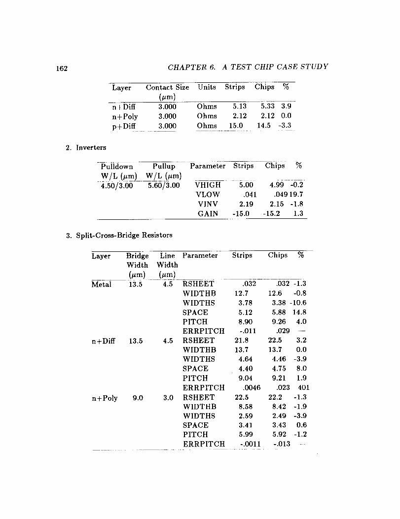
162
2. Inverters
CHAPTER 6. A TEST CHIP CASE STUDY
Layer Contact Size Units Strips Chips %
(.m)n+Diff 3.000 Ohms 5.13
n+Poly 3.000 Ohms 2.12
p+Diff_ ....3.000 _ __Ohms ..... 15:0
5.33 3.9
2.12 0.0
14.5 -3.3
Pulldown Pullup
W/L(_m) W/L (_m)
4.50/3.o0 5.60/3.00
Parameter Strips Chips %
VHIGH 5.00 4.99 -0.2
VLOW .041 .049 19.7
VINV 2.19 2.15 -1.8
GAIN -15.0 -15.2 1.3
3. Split-Cross-Bridge Resistors
Layer Bridge Line Parameter
Width Width
(#m) (_m)
Strips Chips %
Metal
n+Diff
n+Poly
13.5 4.5 RSHEET .032 .032 -1.3
WIDTHB 12.7 12.6 -0.8
WIDTHS 3.78 3.38 -10.6
SPACE 5.12 5.88 14.8
PITCH 8.90 9.26 4.0
ERRPITCH -.011 .029 --
13.5 4.5 RSHEET 21.8 22.5 3.2
WIDTHB 13.7 13.7 0.0
WIDTHS 4.64 4.46 -3.9
SPACE 4.40 4.75 8.0
PITCH 9.04 9.21 1.9
ERRPITCH .0046 .023 401
9.0 3.0 RSHEET 22.5 22.2 -1.3
WIDTHB 8.58 8.42 -1.9
WIDTHS 2.59 2.49 -3.9
SPACE 3.41 3.43 0.6
PITCH 5.99 5.92 -1.2
ERRPITCH -.0011 -.013 --

6.10. MEAN VALUE COMPARISONS: SUMMARY RESULTS 163
Layer Bridge Line Parameter
Width Width
........ (.m) .....p+Diff 13.5 4.5 RSHEET
WIDTHB 13.3
WIDTHS 4.35
SPACE 4.59
PITCH 8.94
ERRPITCH -.0069
Strips Chips %
87.2 86.6 -0.7
13.1 -1.5
4.22 -3.0
4.61 0.4
8.84 -1.1
-.018 164
4. Transistors
Type .... Witi/]Len Parameter Strips chips %
n-MOSFET 6.00/3.00 VT0 .672 .674 0.3
VT1 1.06 1.06 0.0
VT5 1.95 1.95 0.0
KPRIME0 50.1 49.9 -0.4
GAMMA01 .833 .833 0.0
GAMMA15 .818 .819 0.1
DRLEAK 20.2 26.3 30.2
ISAT0 508. 505. -0.6
ISATI 458. 455. -0.7
ISAT5 327. 325. -0.6
6.00/9.00 VT0 .709 .708 -0.1VT1 1.12 1.12 0.0
VT5 2.09 2.09 0.0
KPRIME0 44.6 44.4 -0.4
GAMMA01 .870 .871 0.1
GAMMA15 .899 .899 0.0
DRLEAK 21.1 17.3 -18.0
ISAT0 174. 173. -0.6
ISAT1 150. 150. 0.0
ISAT5 91.6 91.1 -0.5
9.00/3.00 VT0 .669 .668 -0.1VT 1 1.06 1.06 0.0
VT5 1.93 1.93 0.0
KPRIME0 55.0 54.6 -0.7
GAMMA01 .829 .832 0.4

164 CHAPTER 6. A TEST CHIP CASE STUDY
Type Wid/Len Parameter Strips Chips %
n-MOSFET 9.00/3.00 GAMMA15 .802 .806 0.5DRLEAK 14.3 19.9 39.2
ISAT0 819. 812. . -0.9
ISAT1 742. 735. -0.9
ISAT5 544. 538. -1.1
9.00/9.00 VT0 .685 .683 -0.3
VT1 1.09 1.09 0.0
VT5 2.05 2.05 0.0
KPRIME0 44.6 44.5 -0.2
GAMMA01 .867 .868 0.1
GAMMA15 .886 .884 -0.2
DRLEAK 20.9 12.8 -38.8
ISAT0 274. 274. 0.0
ISAT1 238. 237. -0.4
ISAT5 148. 147. -0.7
p-MOSFET 6.00/3.00 VT0 -.835 -.829 -0.7VT1 -1.01 -1.01 0.0
VT5 -1.37 -1.37 0.0
KPRIME0 19.2 19.4 1.0
GAMMA01 -.385 -.386 0.3
GAMMA15 -.331 -.329 -0.6
DRLEAK -20.9 -19.2 -8.1
ISAT0 -223. -225. 0.9
ISAT1 -210. -212. 1.0
ISAT5 -177. -179. 1.1
6.00/9.00 VT0 -.860 -.858 -0.2VT1 -1.07 -1.07 0.0
VT5 -1.56 -1.56 0.0
KPRIME0 15.5 15.3 -1.3
GAMMA01 -.460 -.460 0.0
GAMMA15 -.446 -.448 0.4
DRLEAK -22.8 -25.0 9.6
ISAT0 -60.7 -60.3 -0.7
ISAT1 -55.1 -54.8 -0.5
ISAT5 -41.9 -41.6 -0.7
9.00/3.00 VT0 -.813 -.811 -0.2
VT1 -.984 -.981 -0.3

6.11. WAFER MAPS 165
Type Wid/Len Parameter Strips Chips %
(Urn)p-MOSFET 9.00/3.00 VT5 -1.32 -1.32 0.0
KPRIME0 20.0 20.1 0.5
GAMMA01 -.367 -.366 -0.3
GAMMA15 -.310 -.309 -0.3
DRLEAK -13.4 -28.1 109.7
ISAT0 -356. -358. 0.6
ISAT1 -337. -340. 0.9
ISAT5 -290. -293. 1.0
VT0 -.846 -.846 0.0
VT1 -1.05 -1.06 1.0
VT5 -1.52 -1.52 0.0
KPRIME0 16.3 16.1 -1.2
GAMMA01 -.446 -.454 1.8
GAMMA15 -.426 -.428 0.5
DRLEAK -22.6 -13.3 -41.2
ISAT0 -95.3 -95.0 -0.3
ISAT1 -87.1 -86.8 -0.3
ISAT5 -67.5 -67.2 -0.4
9.00//9.00
Notes: KPRIME --#oCo × 106
DRLEAK in picoamps
ISAT @ VGS=SV, VDS = 5.0V in microamps
VTx, ISATx where x = value of VBS in volts
The agreement between Test Strips and Test Chips is generally within three
percent. In the cases of metal sheet resistance and transistor leakage the dif-
ferences are due to highly skewed populations, indicating the need for a more
effective method of identifying outliers.
6.11 Wafer Maps
The following pages contain selected Test Strip wafer maps from Wafer #10.
The data is presented as avenue wafer maps where dots indicate the location of
the data points on the four-inch diameter CMOS wafer. The surfaces were fitted
to the data using a Bivariate Interpolation and Smooth Fit Algorithm[32,33].

166 CHAPTER 6. A TEST CHIP CASE STUDY
SHEET RESISTANCE
RSndiff (ohmslsq)--2l. 9 • I. ,416.2°1o): ::::::::.:._::x=2%STDEV
• m |kllt+ llJlll m I .....
lll_ l]3]]J]331_J. IIILI .......
_1 3]]13 ........ 3331 Ill ......
• l• 1!, 515:5_,.. _ .... •555 J3331 13a ....[I }_ 55_. ,7772277777777 .... 555.13].1| .....
,1 3 % ..... 7_7)7)3 ......... 7739 .55 33..1 ....
.... 3 557773_7773337777 ..... 7731773 5555.1311 ....
]i 7777;_)?_7737777 ....... )?_7_73 .... 2.315 ._1 5•,rz_. m _m))TTm7 m m.7)?mT))Im m5_J3 l..
L 3572 ...... 777777? ......... 7777777777 ..... 55..11 ....
] 5_ )_ .... 77)7 ........ 77_Z)717_ ..... 55 3 l.,
55• 7771 I I 7,27.1 .... m.. m.zl_lt)lzT_?e++. ,+31e7_' ............. 77 ............... 77_7_77777_.. 5 3 I.
7;7_7777 ...................... 771777_177,.25.3[. •
777777777)7_ ....................... 77777777777...55.3_L +.
. 777773777197 .77737777 ............ 7T7237337773..,_5,3,[,,$55.7771177717_71777717777177.| .... 1?777_7777i777#._•31_
5_.TT;_ZT77; 77;77777777777_P77777)7777771777 .... _ 3_
]3 _ ?_7;_;_7777722777777)77777777777772377 ...... 55 .3 ....
3 _ 77_7777_272777777_7777377377377 ........ 555+,31 .....
_55 _727_7_77777_???7777377777777 ...... 522511 L
l _ _? ...... 777277777? .... 5E55 ,)l 11
Lk i _ _ ......... 777 .... 5555 333 II
It J_] ........ _55_ ..... 3]J] . lit
/iZ 3)33333 ........ 31313 1111 .......
I till l 31331)13) a 111 i ....
_illlI ...... _]IL_I ........
l m _ I. + I
LINE'WIDTH
Wndiff (#m 1=4.58 O.055 (1.2%)+_- ,_...... ,7-- A=_o STDEV
.... --, wo=a.:_ m: m' .I _ • .... i • m ?_
+SmSm5,_m+= _5555_m_-++-35
51¢ 55+ 15+mml+555155551_.55_lSm+Sl • • mm1555+_.
555555m_ ......... 55m5 5_555 m
_ =_55e:5 .• ........ _551_5
F555 .......... _555_
.15_551 .. I... t .... I .m ...I • , m I55_5
.5_5_ ................ _mSSS_m_ 55_5
5_=_=_ ..... ¢.55_5555555_555<5555 _ . 5555:5
_155 .l + I+_5_155_5155_51_155m515 m i I_551_5
555_ . =555555555555_555_5555555=-:5 _35_555555 ...... 555555555555555555._55555_5555 _55_55
55+ I.. 55 ISE 55__ 5555t5555t_555555_ _ .__ , 5_55
555 ..... 55_=5555555._555555555555555555 . _555_
55:_ 5555555=555555555_5555_55555 _ "55_"
55155 I .SISSSSISST_ISS55_5555m5555_ l • • | 55155
5_5T_ ..... 5555555555_5555E5555555_' .. .'_5=5
_55 ...... ¢55555_5555555_.555555 _ :55"5:
-'_+_.: • .+ i. 551555__,555515555155 • • • w | ,:S_
_:_:= 555555_5555_555=555_ ....+'i--i- .i i'_5 55_'_5"55"_._5 "_e "=
_g75=5 555_=5
55_= =315 I . .I_E55155551 i ,
_5:5 _5555555555555555_55555=5
5-lScc=l_5}giS_St}Sc_555_#_5 • _5515_55:5
3313333tm 3333el ) ) +to ) ) ? ?Im
)))l))) _l )IS)))))
RSpdiff (ohms/sq)=87. 2+ 2.0 (2.77777777777777777777777
............................... _=2_ STDEV.... 7_?7777777_)7??77777727777777777
...... 7777777777777777777777377772
.! • _1777)7777?_7_7757777577 .....
...... 777)?7?77777 .........
5555_5555 ...................................... 5
5555555555E== .................................. 55555555.
555d55551555555 ............................... 55555515552
552. 55555555555 .......... 5555 ........ 55 .... 555555555555255555 . 555_555555555 ..... 5555555 ,,5555555555555555555555555
515 I 55155_5•55551_..•5555_5555a5555155551555515555155S25,
555_ .... 55555555_555552552525555555555555555555555555555555
555 ...... 555555555555555555§5_555555555_55555555555555555555 .....
55+ .... I..55_555.$..55t5555t55.1.5_51555512555155515555155..t.
........ s+++5%_...+s+,+,,+s+.:+..... 5.+,s,++,+5+,..... sss. ....................... 555555555 .... 55555 ............ 5555 .......
333 ...... 555_55 ....... 55555.,.33 ............................
331131 ...... 55 ........ 55_ .... 13 ..............................
.313333l.. I .... I...l .... I .... 13+.+I .... • .... • .... I .... I .... I.
+31332 ..........................................................333333 .................................................
131131 • l .... 131 .... l .... I .... l .... I .... 1 111311311331 ..................... 333 ............. 33333+3]33133
,333333 .................... 333 ............... 1113111333111
3313_33..I ................ 311 ................ 333331313333
313333 .... 33313 .............. 111113333333n31_T:::)i]:::;::::..33131 ........... 311333n3n3
3J3331 2_)+_33 • ..1+3)131,1 _|33]1131331333317
3333]3_r?3333J ........ 333333.33333133J3333333_33
331333_333333333 ....... 33333333313333333333333333
333133313333133331 .... 13333033|333333_3333333
33333332333333333313333333133333313333333
13311333313313331_333333)333313133133
IJ33J133331333_l$3331331]#13113
33333333333_33333333113
Wpdiff (#m)=4. 28 0.08 (1. C o)• ....................... /_=2_ STDEV
7:+77777777;777_77777777 77?77 55 +
............................ Wo-4.5pm• 5_•5_5515555m ..... 55#555515555155 .....
5_5_5"_-=_t_S2¶_555=b:b255555_ ....
55555=5f1555255_5555_5555555555 ..................
# ..I . 1.555555551555_#5555e5 # I .... I..
........ 5:555555_ ..... 5 ........... 2
.................. 555 .............. 33 ........... 5
.... I. I ...................... 1333 .... 1 52
........................... I]]3 ..... 52
......................................... ]33 ........... 55
.• ...I • . •. ._.5551E5.1 .... • .... _ .... I .... i .... I ....................... 555_555555555555 ...........................
...... 5 ...... _5555555555555555555_ .........................
--1-..5155--I..555555515555155551555515+t .... I .... I ..I .... I.
..... SSS552.,.5555555_555555555555555f5 ................
..... 55555555555E55555555555555555555_5 .................
,I..$5155551555_55555155551555_555555 .... I. .I ....... I .I.
..... 555555555555555555555555555555555 ........................
.... SSSSSS .... 5555555555555555555555 ...........................
.15_5155.1.5_I$5S51_555•555_155_I .... I .... #1 a.. I .... i..
...... 555 ..... 555555_5555555555555 .........................
15,es55!15555.552515555155 I .... • .... |3J. I ..I ....
5555555_55525555555_5_ .......... )333 ..............;i_;22. 5_5555s_55_555_55555 .......... 11311
.5155•_5525. 555_55_555_5 ......... 131 ..............
.... 555_5G555555 .....................
. 5_ ........... 55_55_555525 ................. 3333
.! . I .... •.555e55551555 I i..i .... I53353
..... _55555_555 ............... 33........ 55_.555555555 ................. 1
.• I.. I |_5555 .I .... • .... I ....
i::;++++J++]++]++++_J+++j+++l++ ::iGs]3333dl]lll]l]313]]31J333e3313.
CC (Wndiff vs Wpdiff)- 0.82Figure 6.3: Test Chip wafer maps for the sheet resistance and linewidths of the
n+diffusion (top) and p+diffusion (bottom) from VTI 2, Wafer #10.

6.11. WAFER MAPS 167
SHEET RESISTANCE
RSnpoly (ohm/sqi:22.4 + O.6 12.7%)............................ n=2% STDEV
]] .5 ....... 55 ..... 555
......... 555 •.55 ....... 555:_
:,_ ,5555#_5555..33m 5.m; #555 ....
5 .57553:5555 333]35. 55555 ..... P?
v,_ :::_s_35 ., ......... 5_=555555 .... 77p
m;;_.4 =_ j .... u .... i .#555m i 5.$. 7777
5..555 ]1 ]J ..... 33 ....... 5,35]]..]]555 .... ;:l
53 _]3 _ ]J]3] 11 3 ........... 3]] .... 3],555 i377
55 ._]_ ...]]_3],Lll ] ........ 3]]3 .... ]3..555 .;g
5 333 ]3_]_ ]31il ] ....... ]333333333 5555
5a ]]_]Ji].]_ # m5]#..]]l .... • I]33313]#.555_55
_55 . _5333_] ...... 33 .... 33] ......... 3]333 ..... 55555555555
55 ..... ]]3 33)333 ]]3] ................ 55555555555
51 # 513 I. #]3] • ]15..l .1.515555#555 #
5 _ 555 .]] 33. 3.55 ........ 555 5555 ....
]]]]i_]]] ....... ]333331 355 .... 333]3.55 ...... 77
5.I 33_J3]]_3i]]]3 I]]13].I.3],55 ]I]]331333.5.1 .... 17_
55 33131_]I_]333]]3] .... L.13.53333333]]333,55 .... _727
2755 ]3]]] 3333 ..... 3 3 .... 3333333333333 555 ;7;
71 55_i]Ii I }ill 51 .]I 33l.]]I]]313]13] 1551_I
77 555 I]!3333]J1] 5 ]]333 .... ]]333 .333] .. 55 )I
35_ 33333 .......... 3333333J]3 ............ 55. 7
I .... i I I 31]]331 .... 155551 .... 1555..
• ]3. 5 ........ 3555 ..... 555. 33]33. 55555555535555
3]3333 55555 553.,333 55555555555 5555
3]]_,_ _ 5_5_.3 55, 5555555555555_555
_3 l_ _Sr .333 555555 555555
] 5t5;::_ 5, ]333555 . _5555 ....
:::_:;::55_:: .... ]_ 55 ;??;,zz,,
_5_5:_555_555_ ;_ 1
LINEWIDTH
WnNly (pm)-2.63 +0. 10 (3.7%)......... 5.... -_ _:2% STDEV
................ 5., Wo;30_5333 :--5 .. _;_Z;7. 5_ _ ;z 55. ]3 .I
3] _. 7?;; . 7 . _? 59 . ?_1 555 3]]]]
3 ]_]..7•77! . 55_5 ; 959. • 55 555 3]_]
l 3 .55555;= 555:_55 ._? 55535 31 1
I ]3 . _i;7 5555555. 777_77;!;_ . 55. ] .
33 5 27; _ . 55 55 _??;_7_ . 5 3 1
53] 5_ 5_5 353_55_:5 3 5,; _7 55555555_ 5_ ] :
55555:5555 55 55 333_ ;_; 55:5 . 55 ]
55535 555_55555 55. 5555_55 55555 3333]
3] :5 5_55 _55 5 55 5_5 55 ]]]] LI
I _3 _:_ 5 5 _7 ]] 5 3333 I] _e
;I ] .: _ --: 33 _ 5_3=5:.5 J]]:_
.j _ 55_
RSmetal (mohmlsq)=32.0 * I. 0 (3.0°Io)...... ' ...._......... A:_o STDEV
i_ I]_71 **1 .771.,_19.
._ 55 ....... 333333].,3333333]]..55 ..........
7_7 555 ........... ]33333].33333]]33]...55555 ..... 37
71 551 3]I]].I,,]I]3].I 333133331]._.15551,,,3.9
7,..55.33333] ....... 33] ...... 333335333]],.5555,7,99
;.5555 .... 3333]]5 .... 3 ........ ]33333]3] .... 55..3..9.
77.# .... _33..33..5555 ...... 5555 .... 3333333 .... 55..#_9.
7_ ........ 3333]3 55555 ..... 55.555 ...... 3333 .... 55,799.7 55 ] ..... 33333]33 55555 .... 55,,55_ ..... 333]3 ..555.79..
7155.@]3 ._ 333|333,#.55#55.#55_5555_ .... _3353e3..#579.
]7.55 33]. 333 ........ 555 .... 5555m55 ..... 333333.,55 9.
_.5_5 ........................... 5555 ........ 333333_. 5.79..
.5#5 • _55#5..# .... I .... #,, .I .... I 33@333.#5.?#
555 ............ 556555 ....................... ]33333335.].9..
5555 ............. 5555555 ............... 5 ....... 313.335,.7.9.55m5..i. _ .... 555#55551 ............ 55# .... #333 .... 3155.;I._
555 ............... 55555555 ............ 5555 ....... 333333355.7.9
55 .............. 55 .. 555 ....................... 333333.55,?_
551 .... #]...I _ .... _ .... # .... l .... # .... _ .... I. ]#33].1537m9
555 ..33]] ................................... 33333.,57 g
55. 3333333 .............................. 333333.,55.79.
155 #3333_3] I .... _ .#. ! #..,I.313333_3_.._57_ 9.
55..3333]]] .... 3 .................... ]33333333..5.779
5 .33333!]13. 333] .......... ]3.3333333331],55 .79
5_•]_]_]J1333333]_] ........ 3]33]]..]333]3 55 7553]]1]_ .]3333333]]] ..... 333] . ]]33. 555 7
55 ]33!_ ]3_]3333333333333333,_ )]]33 5555
55 _•_l_ , ]],3]]_I]3331333]W3_]3_]]]3# _55555
.55 }]_1]]_]_133333333335]]]]3]_33] 555555555
55 33333]]333.33333]3]3]333]55 ......
7# 55 _333_]3331],.333333o3]33_5.e 777777
?? 5h .... 35333333353..3 ..... 5_;_ ....
_9 55555 ............. 5555 ,77799
1. _555535555#5555_.7#).99
7 ......... 555 .... 777
Wmetal (ym)=3.87 + O.19 (5.05)_']................A:2% STDEV
............................. Wo:4 5#m............ :555 ...... 7777; .........
.... a ....... 5555 ...... 55]777] ........... 939
.5555 .5=..3 55 .... 3,.5..37.777 ........... 99_9
55_55 _ 531 . 13313h 577 7;777? _; ..... g•g_ .
555555 5 ] .lIll ])_]]333]. 7 .... 77;777777;_7. .9_9_
. 555555 .:5] Illll ]]33 33.57 .... ]7777777_?_7;. 99999_9
, 55555555_ .]J ], ]]]3]. 5.777777_;;777777_
, 55 ....... 55 333 ........ 333.55.77777?77 ........ 7117
]55 .... 55555,3333 ..... 335.373777777;;7 77777
]].555 .... 55555_55. ]]] ...... 35 .... 3773_77.. _77_?777zz7
3]•. 55_5555#55555 .... •3]].• ..... 3.5 ..... l; # ???_l;._
333...555555555555555.333 ...... 55 ........... 7;?; .... 5
3]]..55555_555555555.33.1111.,] 55555.555 .......... 7777 .... 5
I]3#5555#5555#55 N].IIIII}#. ]I ]]I 5.# .... •,.77i7_ I55
333 555555555 .33 illiil[[[ 333]333 55555555,._ 555
11.33) ...... ]]]31..l[ll]llLi]ll ..... 3] .... 5555 .5555
1#3]_)333,3!_3_ #llllllliIIllllelll|ll ]e., 155_# 55_55
111.3333333], .IlIl .................... i133.55535_55555
,t_3 ...... ]_ ................... t_33 555555555
.I[I• ..• 111l[11 ....... 11 .... I 33 . 55555555
lllll ]Illl .I .... 1I!11111], ]1 33 5555_5
33J3]!J ]A3333 ................. ]] ........ 5_5
33]3)]3]]33]3]33]]] ............ 3]3],555555555
# _ _3J3#]]3 _ ]_]] 155 55
33]]]3]]3]] ......... ] 5 77
.]]]]]]3]]]3]] ....... 1111111 35. ?] I]3I]] I.llII_ # 1.3
I .... 33511II ......
Figure 6.4: Test Chip wafer maps for the sheet resistance and linewidths of the
n+po]y (top) and metal (bottom) from VT] 2, Wafer #10.

168 CHAPTER 6. A TEST CHIP CASE STUDY
CONTACT RESISTANCE
RCmndiff (ohm)-5. lg + 1.43 (27.5+/o),, .,_,:.. ,, ...... ............ A-8% STDEV
] .71133] II ........ It .....
J_l]3]]].]3)]33.H ...... I..LL ........
_]_3_37#]# +#.]]].l|lfl|l,J[l,+| .......
.33 ......... 5 .... . .... ]]..ii|..ll ...........+33 ......... 555555555555555...33.1111|11 ..........
]l...515_551_55.1.555dS..71.551.ll[i..Jl...I ......
]..555,5555 ....... 555+7...7.55.]5 ..... 3_ [ ..........
.555 .............. 7 ..5555.7...] 5..3 .... 53]]+Z ..........
5 077571 7 ......... 55555.77.755+3...53..]11+.,e ....
.7777..339997 ........ 5555555...755.33..3775..33..1 ........
777,. 9 ...... 777 .... 5553355553, .5.35353.+$ .... 31 .........
.159e. | 177771...515555155.|55.)m]3..1...3|1.0 .....
,.9_9 .......... 99777 ............... 55..]J5] .... _33,,_ .........7..g5 .... 95955.999.77 ........ 7,77 .... 555 ....... 33333..1 .........
7.|95.e._m .9 d957_.555..971.77 0.5551...5i3555_ .]|I .... |.+..99 ..... $ 5.+ 97.555.7 .... 7_...555..333 ....... II ........
++.99 ............. 9+7...5555..L59.T7?P.55+5..|l|XL. lll ......
.#99.• .... a .... @77m+555#55.7?.99...P7.BS.3.#l...ll|lll .... m..
.... 7+.9 ....... _9.77..5555555.77 ....... 77,5.3.L],,.11111 .......
.... 7+.,_5 ..... 5..777.555555 .... 77 ...... 77.5.+3.11 .............
..B�.].m.._+i .91777+1515...I..7]157.,_]..5133,1D .... I .... 0 +
7.,3.3 .... 3.9 277777_ ................. 7777+55..5,]1] ..........
55.7_ .......... 7 .... 77777 .... 7]]77] ........ 555 .33 .... |[ ........
+..I .... _9 51571.77.#+]7.B7,SB5555_.1553D..[ll .......5.79 ....... 975,57 .... 77.77 .... 7,5 ....... 333,..353..,1 .......
.575++. 99 .5557.9_,777,9.7,.._3533555...3]]3...| ......
.57I ,_i ,7.5.7._5 7...7 .... 7.5.333353333.3333..1 ......
5..7 ..... 77 3 _ 5 77,._,5_],. _35353J.,1]1 .....
5_., 377779.3555, 777_5..33 .... )]]3..lZill ....
)3+.5 .55555.]7._.,555555,,,333..i11llI ....
.33] ........ _5555 ......... 3333+..11 ...........
_1| .333335333333533 .... ||_l .........
,|ll ............... IX1 ...........
llillillllll_l| ........
RCmpdiff (ohm)=14. 8 +3.7 (25.2%).......... 55.+.+,.. A 8% STDEV
_77757_ 775_5,,_33 ...... Ill ....
_.. 7175_777,.,5555..]]3 ,Ill|l|.
9+99 .... 77777.777..:55555 ]],.Illlll., .......95_ ...... 777+,.P? ....... _.]l_ .... lift+.
+137, I i..+I.]..17.+71.511]] I ll,,l .....
,9+++5 ............ 7.5557]]..5..]JJJJJJ,.,| ..........
+.9559597 ..... 77777,,7+155,]773.555 ....... 3.,1 ...........,91999515,..77 .... 7.7) 55,7717.55555555,3].I| ...... I
.99799099..77.75.557...7.55 ......... 555+J..[t ........
99_9_999.77..5..5.7 7.5555 ...... 55..3..L| ...........
,I. 91599919_+.#7.55t5 _7_77,505555_5_5515,33•.11+i .... I .....
• _9999595_]..777..555 7777.55555555555.3]...[[ ............
,999.99999_ 7777 553 ,, 333 Ill .
.lYY• 99•99 _277717,+I . 5_55.,1533113..iLL11 .... I .... I3999 ........... 777 ........ 55555.333333333 ..ill .............
......... 777..555555555555..]3335333 ..... 11151]l .....
.i_777_7777555155551555555+353533153.1 ...... lilt .... I
....... 777777_?17.55 ........ 555.3]33333]3 ..... |_]lll .......
777 ..... ?? 7755 .............. 3]]3335]..1]|11111 ......
77.7.._ 1775_ ...| ...I .... 131331]].1[|1]t1L..i I7 ............. 755...]3..35. 333]]] . ill|Ill ....
......... }7 53 .... 5555 ..... 33]] ...... kill ..........
9_, ..... _9 _55 ..... 5_55555_,J]]]j .Ill[ ....
399 .... _77_9"197.55 ...... 555555..]533333 .... |ll | ......
i ,71,2 99_ ]55 ..... 555555.133337 .... lllll .....
..... 777777._9.55 ....... 5555 ]]]_]l .... IIllll ....• 77 777. +75 ........ 55 .... 333333 ..... llllli
_7_7_7 555 ..+5 ............ 3333] ..... ||ILIIi
77. 5_5555555_555 ....... 333 .... ltllll_|
.+_55_ _ _.55155 + 1.]l]._illtlll
555_55 ...... 3]]37333 .... ll/|Z]lt/555551555 _ .311 .dlllll .....
5355 _l llH|| ....
RCmnpoly (ohm)-2.22+ 0.43 (19.3%)
....... ' -']"' ...... A=8% STDEVI 5#.5.31 .... i]3))e).l|l
.... 555.]] .... ]31533].i|ili .....55551.33333113.35333313+.1 ...........
..|5551 33|+ .13]33533)a3.|+1 .... I .......777 .... 5535 )333333533 ..... 3]]5.IILH ...........
7777,7.... 555555............. 5m...u_... .......,l,,_ItT.._ .... 1.5551555_$..3_33331J..Z•I+ +• ......
.+_ ...... 7777..7777...555_555..333 .... 3..lll_ ........
..$._$9_...77777_777 .... _5...55.]53] 3 .]llll .......
..51_5_I. 7777.7777_1+5555555,33]]33 ........ lllll ....
775935559_ 7777 77.55 ...... ]3]..3 ........... llll .....
77_7777 .... 777 ........... 53 ....... ]]J ..... 353]]] ...... _ .....
...................._55 777.555 ....... _333333333.35533.._|.
77777;]7..5555 ..... 55555.7777..§55 .................. 333,1li .....
771_77_1.5515555_5555_5 7177.515..I .... I. 1 .... 13..11 .... I +
...... 7 .... 55555_5555 5. 5_555 ........... 3333333]33 l| .....
555, ........ 555_55555 .......... 5 .......... 53..llll..33].t[ .....
,515555t .... 155555555._..]]1333 ..... 33 .... 133,II .... L.3,111.1..5533555 .... 55 .......... 333_3333333333 .... ]..it. .ll ......... l
............. 53 )]2]+.5.,_33353333]]353.3333...1_Z111_1il .......
7717,.,I,..•5_ ,I]3 5•35#]] •]]]]l_]])•SJJS#. IH]I• .... •...77 ......... 35 .... 5555 ...................... ]]]33.H ......
.55,,77777 ..... 55535555553.,.$55555 ......... 5555 .... ]].1 ........
._5.7177771. • .... |.555155..I.55,1..'5155._,$51.3.|I ....
.53,77 .... 77777 .... 777.,,555,,77755,.55 ............ _..|| ....
35,7 ........... 7, .77L.5..7,,,77._555 .... 77 ..... 5].11.77.199994_9_d_9 7 .... ? ...... 7..55 .... 335555 ).l|
.775.99_9 ..... 999; .... 79_9..77 ...... _5 ..... 3 |l
7.._.99999 ...... ]9_,7...7]. 9 .... 77,,.5_5 .... 155.,11
,.,5_5199_51)95_177.1..771.7177.1555.1.5]]I.H....99 .......... 7..55..77_77_?7 .... 5_5 .... _]5..II,
............ 7777.,55_5 .......... 55555..33.L|.
._7777177771..51 .... 55551555515555155..3 I
77Z7 ......... 5_555§S..5555_55555555555..
_.5555555555 ..... 7_7..555 ....... 5555
..... 155•,7,177+51 3313]]3+
J33..55.7..9.77,]] ....
CORRELATIONCOEFFICIENTS
RCmnpoly RSncliff RSpcliff RSnpoiy0. 66(a) O.66 -O.75(a) O.
RCmndiffRCmpdiffRCmnpoly
RCmpdiff
0. 80(a)
a:CORRELATIONDUE TOCONTACT CUT.
-0.19
Figure 6.5: Test Chip wafer maps for the contact resistances of metal to (1)
n+diffusion (top, left) (2)p+diffusion (top, right), and (3)n+poly (bottom, left)
from VTI 2, Wafer # 10. In the lower right hand corner is a matrix showing the
correlations between the different contact resistance wafer maps and between
the contact resistance and related sheet resistance maps.

6.11. WAFER MAPS 169
THRESHOLD VOLTAGE
VTOn (V):0. 680+ O.009 (1.3"/o)]_' it.......... A=5 mV
J 5' J _ i111,111_
..]1. _33]J]33] _ t_ 5_ 33:]3333
*t J.-_,J. • • 55 # 5 3133331],_l=_ • _3 1
_3_U 5 3 ]335_55 Jlll
]] _+. J]]] ) 7 5] . ] 55_ JJJ +
J 3_1533 i ]]_JJJSt333 } 55 33 3]33] _.]33]] |lL
3]33]]]] 11113 _LL ] 5_5 5 .33 333 ]]3131 [1
J]J3]]3333]_ls] 3JJJ . 3 55_ 5555 3333333J] IIi
#33331331 , .3_.]33J1333 • 3 i _5#555515555#5 • •.J ll
333]3 5. 555_5555555555 ]J 11
• 5551 333. _
_555". "7; 55_5=_ _77 ] 335 _: 7_77. 55 H] 1
J •= i . , , i _• 55•_: i 55155::•5 • 5_._
. : _7_ 555 555_55 . .555_
II_: _. i • •?'7 # I" , ;_ I'_ #. _ i '_ m55 • •.555
: • :5-: _; _ _' 5.2311 55
. .+ ]. _? _, ]33] 3]3 _c
.2 = , = =55_55=._5555555 5 3]J
.; • : : • :_:_-_5+: 5555 _== 555 31 ...
• ".+_:::+::_ • • •1555*55 !_: 3l ...
• ,,,_• ._ • +)# .. ]J• 5 2#7/? # ::
,it L. j_ 3_j J_il]33 55_Z75:7 %_._. J3t3_,, ] ."'"
5_,_% _ 5 J333
VTOp (V)=0. 810+0. 012 (1.555....... ' .... ' ..... 5mY, z;,7 5_.5 9, t7 J 5 _=
;:;.: :5. 5 + 1333.33 ....... 5 79,
55":<_15 i 5 ]i 13 33313].155S51 77.
5"+" :: ;: : 1]J_ 31333555555555 ....
55555 2777777 55.5555557777.3,3.5555555
t _:L_: .;?; . 72#7 1 77. 9_• 31115 # ....
3255 T, _ ........ _77. 77 93_ 95 13 333333J
333_ _i : ? .... 7277 7 9 3 .... 3t]3333]
"]3] 7 55555555 53 .... 53.I 3111 Ii
I 3 5 ?) ] 325 777 5 .555_..3335 7 53 33] I ....
+l_ _+ - _+, _ * 5 :•75 1 55155 .# 5,55 3# 3}I ill .
till 33 _D _ 7 ? 5 55 ..555b5.333313 11 .....
3i.!_ .czt_;, =_55 _ +, ;5 55_ .'_ 5 333 333 I ......! .:2 )1_ 135152 i d] 1331 l l
]]]]3 ]! u+; 9 b 55 +'9 .5753533. 33] I .......
15135]+l]3J _5:5555 +7 55 5 5J33333333311 ....J]+_l+]/ +.15 5555551 5b51 333 5+ 5 5333 13333 tltllllllil
]J3] 55555555 5 555555 .3JJ 5 _ 5 .13 33 kllllllll
]3 + 5555:: .......... 3 55 55: 555553lli. It 3]
# 551 _551 # 5155 # 3]]1 5 15155 15 31L[l 1 .i]
3J ]3 +5555++, L5:555 .... 55 77722/ ...... 533331_lI .33
PP lit+ 55_ t+5555m5555555 759.;77;55 3331L[1.33
;I55331 135 •: # # l? 31 9 e7 51 #J311[ 13
+ ?g] ! 5 + ;, :F?;+t77? ..... 9 7 + 55 3lilt )
+ P 553?+,,+ "_ 5 7+7 ; 3 5 5.3 555,3 ILLLIL[
_+ . • j+_! :! •_ + ! +?99 523 I 555 I l_, ,,+'+ ]+ 5 + ++++ _ .5_5 l
J'J,lJ _ "+ i :_ 1, ;? 531 J.55Jl ....
+- + # l 15 +;t l%][lt ]515 J•i J +, ,' :J t 555 55 3 555 + 11
' i+]i]j]j]]]] !555555555+55 3 i
::. + . ]]+]]]J#l]]l 5555+555515555155531
+ l ]3 ]]]]] +b 5555_35_
]+ ] 5 777772555555, 717
+++•- 155?1 1751 55
_555_ 5 + ++ 35
CONDUCTION FACTOR
KPn ( uAN2)=47. 6 2_1.4 (3.
............................ A=2% SIDEV_ I 533 1.33313.5555555555
_5;;355. 33. ..3333]] ...... 555555555
I 551551, 33133333333313...M .... I .......
5 _g_55 33_3313331 ...............
55 .... 33331 ................. 333] .... 11]]3] ........
515551 331 13.# .... I .... I 331333_3111333t ..... 53 11L3 ..... 555555 53 .333 33 3335. 55
333i .... ] t1115 ...... 5555553.1.3331. 3333].. 555
55. #]]31 31 ]5 31 3.55555331111 33333. 333.#5555
.5533113 ........... ]]1.3.55555.3..11..]...3313...55555
,,55 ...... 55555555555.3,11 .... 55555.+31111.1 ..... 33]]3..55555
71555155_5551 551331,33.1555515 ]l•].155. d., ,1.5555
555555555555 5553333]3.55555553355555555 ...... 55555
555.55{55+5_555_55555.. 3_3. 5555555555555 ....... 55555555555
5515555#555_I 55155551 .... # .... 155.1 .. I 1.77#3155551
5555555555 . 55555 ........... 55.71_ ...... 77777 .........
555 ................. 33.557_555555555 ........ 55 .7;
55# ]11233113]]3 .... I I13133355 .5 I . 155555555515.1;_
.53 3333]]]333333] .... ]] .... 3.55533]3] .... 331]] .555.,.77_
77 55 ...... 33 ..] .... 555 3 .... 3 .... ] .... ]]]l) ..... 3.55 ....
9 I;551 .... I 31 1
+?_55 ...... 33 3 ...... 333333333 +ill .... 13 ..... 555..
77 55555]13333 333 .... 333333 ..... 3]3]333.5555
_E5 15555• 3+•331 33133.•|5..31333 1 .... 1333133 t3.555555555555 3_3333 ..... 333] 555533]333 .... 33.3 ] .... 5
555 33]] 3]3 .55 3331 5 5333333. • ]3 33 ......
t._] •]3 5_]].55 .... 555 ] .).3 .....
333 _ 5. 55 555 55555_ ] 3555555
5 _5 _77_ 5 555:J5 555555_53 ] 55555555
'7, 55555555 .55555 555555555.
.;'_:7_ 55_55 .... 555555 .............
;_5777•7 5155.1 .55555_55 1377717777_7
.... 7_77H7. 7775555 .
]_9991971 91 ; 5155 _ 7_
39 .... _99 55555
KPp (p.A/V2)=17. 6 ± O.9 15.I%)............. 3......... A=_/_ STD[V
..... 11333133]]1333.1++ 1.. 33
.1.]3333 .... 33333..+55555. ]Jl
...... 55 ................ 55 .... 5..]].ll
• i _55 1 .5t55 .... 15515.133..tl.
...... 3 5565 .... 555 .5 33] lilt
...... 1333333.. 55 ......... 5555. 333532 .....
• 31.]+]3331331 _.1 .... I .... #]]3 l .... 1 .333+1.555 .33] 33333 ............... 333+.II..333333.,5
..... 35.3 ....... 333 33 ...... 333]. 1111.,.3133..,55
1_ ]313 .... Ii it 33333 ..... ]3]llltt .... 333,1.555t{illll3 3 .... lit ..... 1 .3.55 33.111 .... 333 .......
I It 33]33 . It .... t 35.+333 .......... 3355. 333,
31 ll#lll _.. Ill 1.111 3.1..3133..1 .... 133 515 3 .l
333333 II 3333] ..... IIII1 .33 ...... 33333 ..... 33 ...... 1
3333 55.+3 .... 333333333 ....... 333333333 ...... 3333 3333 ...... l.
+1.55_5 .3•]]].I 331333.1333313333_33..I.,.31333.1 .... • .... Mr,5555555.3333 ........ 3333333 .... 3323,.5555.33 .... 33333333+ ,l
555 3]] ....... 555 ............ 5 .... 55...5.]] .... 3.55,55 +]33]
15.]ii] • .... 5555#555 I 55.555.7_.,5.•]335 .77_5 I.]
?_? 5 3]] .... 55555555555..5.7.37_. 5. 33]35 .... 55,
_755 .............. 555555555557???55.+.55..3]]355555..33+
I;? _5551 .I .... • 55.1.551555.I.55.1..5515..]13 I ••35,.
?77 Y? 555555555 ..... 55555555555555 ........... 331557 _55 55555555..775 ..... 55.555 ......... 555535 1
37 _m ? 5,55,5.?e;..515_371_ 313].5155 • •.#5555#5,]].3 5. ._5555 .... 7 .7 5555.777.3,3555551 5555. 5 ]]
3 55 777 .... 77 ./555 7?775].35555 ..... 555...55..]]
] 5#5 T#7_ 77 . 5 5 7 3335 _5 .55 .... 5555.
_ 55 _:_ _3_?<.s _ +_555__5_iii._5 ..... 55555_ .'_ .77_7_77 .555555 ....... 555_ ........
# :'+']75•2_I 55155 # 771 ,5•55 i _7
_ f5 ??TrT;;,'Tt7777 ....... _77777_77 ..... 7777
331 _ 7N 7771727717777777?7# 7..#777 I .... ?3_ 5 7 777:?7777 .......... 7_? .....
5 77 _?.9_55g_9.9999 77
/.399#9 1991 99#99995999
59_ 9 .......
Figure 6.6: Test Chip wafer maps for the transistor threshold voltage, VTO,
(top) and conduction factor, KP, (bottom) for n-channel MOSFETs (top) and
p-channel MOSFETs (bottom).

170 CHAPTER 6. A TEST CHIP CASE STUDY
INVERTER THRESHOLD VOLTAGE
VINV (V)-2.19+0.013 (0.6%)_]5................... ._5 mV] 55. 7 5. 9 _} ........ _=
I } 577.9_99,,I ..........
.i .>31 .5_,7/, 49..7 ......... lliIll
3)1 ]Ill 31..5 I ?77 .... 7l,] lllll .......
_1 .... 55,??1...11.533]]3333]))
55555_5 ]5..5.11...7 ..... 5..95 ........ 113333
5155 # 555o55 11511157,1.75131515555t5 I., 3
555555 555 7.7 .... ].,9553133.5.5555955_55 ......
} .. 555_5 77937 lIl .... 75335,759..55555555.555331 .... 1555 I_3 ..... 3.,_55_,3_$77595_5_5555515555
1.1 ...... _ 79.37.1L..1 31.I]5L9,555,..55555 55 .3
.......13 ]33 55.7 ..... ?_)..llll[ .... 5_759.7 ...... 555..37..31,
7l 3..15, # 517919..,i]]]II]..]15J1791,-gl ,7 1753,,
...... 55555 5_511 .... 5555 ........ 55.7777.5 .... 5_..77_5 1.
?_555555555555555 ........... 1777 55 555 7 .......
,07157 5.55. m555,e.777e777_m7777eT.Sm..�#5 7 e;sa.t7 .333 5 71,5 33333..55..7L9.77 .... 7.,5 ..... 555_77 .....
L531.135._ 7531]1_ _L.55.7.5..77#7555_7 5,333.5 .... 5.1
7as37.tl | ) 5 ]) • 33_e 5 .9 555 199e_._Sm,133.5 19) !
77 531 i,51 5 3_31_)_ 5.?.7.55.7 7 5, 95 55 ]
_9.7.9 _99_ 7 55 55533 5.7775..3,.55.7.595555.. 553
9e 7 e 7_ I ? _59 • 5 .15.715,31 33155 1,5 m55 1 55_5
.9989 . 9 _755 55.55. 5..7.53333333.5.,.5 3.,55 555555
9 . 99,,_9_$ P5533]3. . 55.7_55..31333355.95 .... 3.,555 .....
9gl_u_ _ 5.33...11.i5 771_ 5,|131311 51 til.3 15 7_
_9_9_ 1 _ ]]J lill ]55 777. 5 31331 5 531 13 5 _?_
..99_9 ._53] [) 1 955.7775 .... 3 ]53 .... 57799
91951} 33 1.3...55555.3._5553l I ..... 13 7 3
#J_?5 ] tI 3 ]]33]333333133 5 ........ 5.1
7?771E_ t 3 .3]333 ....... ) .... 5 ...... 52.9 .
_5 55.] iI 1_.333i3 t]1t. 3.55] .I)_ 7 s,
533J ilt_3_33333333..tll13 .)Hi 35. .
11171 I ..... 3333. lLt. 3553_ ......till 3 .... It11.333331 .... 55,5.31 ....
[ . I 1.1_13 /555513_71375 1
7 13 5 _77'i9"1
INVERTER GAIN
IGAINI :15.74- O.7 (4.5%).9_7111ill _J3.5..... ,,53 ........... 55...... A =201,,STDEV
,.1...7,.75,333333,.,555.1..53,1..,
.11 .... 7772,5 ....... 5_55.,_7.5.3,13.,.
,ill 137177.5@_55555.177717 5.i3.1X..
i1.3333.5.77317 .......... 77777.7_75331>
.. 33..555 .... 777777_7777777777_ 775533,1i.
.133 !_.71777717_771 .... I._71_,,919.771.5,,131|1
.33...55.77 ..... 77777 ...... 9 ....... 99..9..7.,55..33..1l
,33..595 7..999,777L.,9999999 ..... 99...9..7..55,3...11
33#555.1777 ..... 777>,9_99 ..5_ ..... 99999. 77. 55 331.1l.
.1.3..55...77777_77.77,,999 .... 99 ............. 775r33 ,|1-,.1..333.59 ......... 77 .... 99999_ .... 7777777.7777..5 .3,1 ....
,11,,,1355l., I .... #,777i .... 4 ...17777@77171777,15,.31,i ....
.11.3333_55 ........... 777777777.,777777 ............ 5..3.ii.
.355...7777 ..... 777777?7 ...... 77377 ..... 555555...55..11 ......
5333395.37771777 ..... 777_?..5.5_ ....... _55,55. 5531 .....
3133333155 ....... 55.77777..3.55 77 .... 55555555595 311 ....
331]3.173.51 _55_1571.793+35,7777,+1._51559 .... 331|1.1
333333, ) .5. 555555555.77.51 .... 7..77,..555555555..33.11 .....
.3333133 55 .... 5559555 ...... 533.3,7..77 .... 555555555.3.1 .......
.)#3)315717 5155 • 5i5.3]i),71#77 1,55155515.3.1 .... I333 .... 55_P_ ............ 955 .... 9.77777.. 5555555 )illl..
.333..55555 .................. 5955,7777 .... 5555555555 33. 1 . .133.l_5551,717/71777•> 1777177,.#555l 55 155 31 I
,333. 5555.7777777777777777...7777777..955 .... 5 ,55 311 ....
,.333.95..7777 777777777 .... 7_7777 5555 .5 55 II ,
,13351 7777 777_ 7_959 ........ 59_5555.5] _1
.... 33.555 777?? ..55..551555555555555i5 l]ll..... 33 59 _ 595 ...... 55555 .... 55. ) ii
I ..... _1_13_ 55515551331 i .... I,> 1171i ....
il ...... 7?31 .... 31333]3 ....... 3313i33 I1 ......
1111117...313333313,.33.._.. 33333 .... 11, .
llllll .......... 33,._55..33 llil,,.
111111lll .... 333..595533.1111
,,,..,..,33..55.5.1. WIlllt,ll3 .59, 5
CC(VINV vs VTOdiff)-- -0. 17
VTOdiff : VTOn-IVTOplTHIS CORRELATIONEXPECTEDBUTNOTOBSERVEDBECAUSEVTO'sEXTREMELYTIGHT.
Figure 6.7: Test Chip wafer maps for the inverter parameters VINV (left) and
Gain (right).
CC (IGAINI vs Wnpoly) : 0.82CC (IGAINI vs VTOsum)- 0.54
VTOsum = VTOn + IVTOpl

Chapter 7
CRRES Project
171
172 CHAPTER 7. CRRES PROJECT
7.1 Introduction
The JPL CRRES Chip is a full custom test circuit designed for inclusion in
the Microelectronics Package (MEP) of the Combined Release and Radiation
Effects Satellite (CRRES). The JPL CRRES chip consists of three operational
test circuits for space radiation testing: a Static Random Access Memory for
evaluating single event upset rates, a Timing Sampler circuit for evaluating
radiation-induced timing degradation, and a-32 cell Transistor Matrix for eval-
uating the radiation degradation of SPICE-like transistor parameters.
The chip was fabricated at a CMOS foundry and parts for the MEP were
delivered to the CRRES program in March 1986. Parts were also supplied to
the NASA/JPL ground test segment of the CRRES program.
7.2 Purpose
The purpose of the JPL CRRES chip is:
1. To demonstrate the viability of using custom VLSI circuits in a spacecraft.
2. To validate the JPL microcircuit product assurance technology approach,
based on the use of a family of test chips, for procuring custom ICs.
3. To provide a transistor-level understanding of the radiation response of
VLSI circuits fabricated at a radiation-soft silicon foundry.
4. To correlate the space radiation response of CRRES chip parameters with
ground radiation tests and to provide worst-case circuit design guidelines.
5. To evaluate Single Event Upset (SEU) and total ionizing dose (TID) radi-ation effects.
7.3 Description of CRRES Chip and Foundry
Runs During Reporting Period
The JPL CRRES chip shown in Figure 7.1 is a 3-#m CMOS/Bulk p-well space
radiation test chip containing three unique experimental structures: a transis-
tor matrix for parameter extraction, a static random access memory (SRAM)
for single-event-upset (SEU) detection, and a timing sampler for measuring
radiation-induced timing degradation. The JPL CRRES chip is included in the

ORIGINAL PAGE IS
OF. POOR QUALITY
7.3. CRRES CHIP DESCRIPTION 173
T$ T$ TS T$ INV XT INV INV
O1 D0 SPARE SPARE SilARE SPARE SPARE SPARE E i SPARE SPARE N-GATE WELL WELL V$$
24 23 22 21 20 19 18 17 16 15 14 13 12 11 10 9
TS D2 25
TS D3 26
TS 04 27
TS D5 Z8
GND 29
RAM DQI5 30
RAM DOI4 31
RAM DQ13 32
RAM DO12 33
RAM _:_11 34
RAM 0010 35
RAM DC9 36
RAM DQ8 37
i
RAM DQ7 36
RAM D(_ 30
RAM DG5 40
T64-STAGE TIMING SAMPLER INVERTER
TEST STRIP __
4 x 8MOSFETMATRIX
INV P-GATE
iNV VDO
INV SUB
5 INV OUT
4XTVG
3 SPARE
2 XT VP$
1 VDD
_84 XT VD
63 XT ID
82 XT C2
61 XT Cl
_XTCO
59XT R0
UXTR1
57 SPARE
41 42 43 44 46 41_ 47 46 49 50 51 52 53 54 55 56
RAM RAM RAM RAM RAM RAM RAM RAM RAM RAM RAM RAM RAM RAM RAM XT
DO4 DO3 DO2 DOt DO0 $ W E EP A5 A4 A3 A2 A1 A0 EN
Figure 7.1: The JPL CRRES Chip which is 6.9 mm × 6.8 mm.
DESIGNED DEC. 'B5

174 CHAPTER 7. CRRES PROJECT
Microelectronics Package (MEP) of the CRRES satellite (Figure 7.2), presently
scheduled to be launched in the early 1990's. The CRRES chip also contains
several circuits for ground test: a stand-alone six-terminal inverter, JPL para-
metric test strips for process/fabrication assurance, and (on early versions) a
ring oscillator for obtaining timing data to confirm timing sampler results.
This section provides a brief description of the design and function of the
JPL CRRES chip and a description of results obtained during the report pe-
riod. Pin-outs and timing requirements for testing the chip can be found in
Section 7.10. The JPL CRRES chip design and function are described in the
"Product Assurance Technology for Custom LSI/VLSI Electronics" report for
the period October 1982-September 1984 (JPL Publication No. 85-76).
The 1 kbit Static Random Access Memory (SRAM) is organized into 64
16-bit words. The SRAM utilizes either a symmetrical or an asymmetrical six-
transistor SRAM cell. These different cells allow investigation of changes in
upset rate due to geometry and are described in Section 7.4. The read/write
circuitry (Figure 7.3) allows full static operation; all timing data is for minimum
execution times for given operations. This design is expected to be the least
susceptible to radiation-induced timing changes affecting SEU results.
The transistor matrix (Figure 7.4) is a 32-element, Kelvin tapped, low-
leakage circuit for extraction of SPICE-like parameters. The device under test is
powered by a separate supply, allowing sub-threshold (pA) measurement. The
matrix has 8 columns of 4 locations with either n- or p-channel transistors (Fig-
ure 7.5): 29 of these locations contain normal gate oxide transistors of one of
four sizes (Figure 7.6). Two locations contain n-channel field oxide transistors
(one poly and one metal gate), and one location remains blank for measuring
total leakage when all transistors are off.
The timing sampler (Figure 7.7) is a chain of 64 loaded inverter pairs. It
is tested by sending a pulse along the chain for a given time. The number of
stages that the pulse passes is presented as a binary number. Thus, in-space
measurements are simplified. The timing sampler circuit and test results are
also described in Chapter 3.
The chip was fabricated by the MOS Implementation Service of ISI (MOSIS)
and by two foundry submissions (Foundry 1 and Foundry 2) to enable compar-
isons of radiation hardness of different processes and manufacturers. Table 7.1
lists the foundry runs used in the development of this chip. Electrical analysis
of Foundry 1 indicated that the lk SRAM chips were only nominally acceptable.
The yield was about 20 percent at the wafer level and the chips were latch-up
prone. The dominant failure mode of the remaining lk SRAM chips was high
leakage current (on the order of hundreds of microamperes). The 4k SRAM

7.3. CRRES CHIP DESCRIPTION 175
POWER AND
CONTROL BOARDS
TOTAL DOSE
INNER = 2
MIDDLE = 8 J. kRAD(Si)/YEAROUTER =340
EXPERIMENT
BOARDS
10-MIL ALUMINUM SHIELD
MICROELECTRONICSPACKAGE
CRRES
Figure 7.2: The CRRES Satellite showing the location of the Microelectronics
Package (MEP), the expected doses for the various experimental boards, and
the locations of the 12 JPL CRRES chips denoted by A1-A4, B1-B4, and C1-C4.

176 CHAPTER 7. CRRES PROJECT
Table 7.1: Summary of CRRES/MOSIS Projects as of March, 1987.
PROJECT MOSIS -- DATES -- ADDITIONAL
NAME(S) RUN SUBMIT PKGS RUN(S)NUMBER OUT
RAM1,RAMIB,RAM1F M65P 5-20 7-23
CRESCHP18_B,CRESCHPI8_A M61P 1-8 2-21CRESCHP17_B M5BG 11-22 2-7
CRESCHP17_A M5BG 11-22 2-7CRESCHP16M M5BE 11-5 1-29
PADTEST2 M5BE 10-28 1-29
PADTEST3 M5BE 10-28 1-29
PADTEST1 M5BE 10-28 1-29
CRRES4Kg,CRESCHP16 M5BE 10-17 1-29
CRRES4K8,CRESCHP15 M59A 9-26 1-28CR4K7TS,CR4KTR,CR4KTM -- 8-17 *CRRES4K7 M56G 5-30 7-23
CRRES4K6 M55C 4-24 7-16
ARRAYN1,ARRAYP1 M53X 3-12 t
CRRES4K5 M53X 2-15
PADTEST M53X 2-18CRESCHP14 M53X 2-6 ?CRRES4K4 M52S 2-6-85 4-8
PADTEST M4CL 11-19 2-5
CRRES4K3 M4CL 11-19 2-5
CRRES4K2 M4AD 10-17 1-30-85
2KRAM M49A 9-13 12-21
CRESCHP12,CHIP8284 M48V 6-2 11-30CRESCHPI1 M46M 6-19 9-13
CRESCHP10,CRRESCHP8 M45H 5-23 10-10CRRESCHP7 M44E 3-30 6-19
CRRESCHP6 --- 2-29
CRRESCHP5 --- 2-28 $CRRESCHP3 M42X 2-1 fCRRESCHIP2 M41V 1-16-84 4-11-84
CRRESCHIP M3AJ 10-19-83 t
M57QM54A
M54A,M57Q
M58U,M63EM54A
M54A
M54A
MS1P-F
M4BG-F-M51R-F
M4AD
M49A
M47T-F-M48V
M46M-M47T-F
M45H
M39D,M39H,M3BM,
M3CO,M41V
Notes: CRRESCHPn = Ik SRAM VersionCRRES Chip
CRRESCHPnM = Ik SRAM Version CRRES Chip, MOSIS/MIT I/O Pads
CRRES4Kn = 4k SRAM Version CRRES Chip
ARRAYP1, ARRAYNI = I>-or n-Channel Kelvin Tapped Transistors
RAM1, RAMIB, RAMIF = Normal, Asymmetrical, or Faulted SRAM
*DELETE-CIF; tWAFERS FAILED; SRUN CANCELLED

7.3. CRRES CHIP DESCRIPTION 177
ADDRESS DECODER tVDD
...... .__ __-____-__ _-L_.L_L.__ _ _ _;_ _o.II___HOW.,O._t,N_O_,_fl I'_^'_-_-"_^'I
r Vss_ t ' -
co tRO I_ L4--___
I
ROW1
MEMORY CELL
SENSEAMPLIFIER
ENABLE
DATA LATCH
PRE-CHARGE
PREC gE TRANSISTORS
R/W
TRANSMISS ION GATES
R/W
_-_----- TRI-STATE ENABLE
I ('T'-HI Z STATEI
IITRI-STATEI/0
J
Figure 7.3: JPL CRRES chip SRAM logic diagram.
chips had zero percent yield; the dominant failure was very high leakage current
(milliamperes).
The 4k SRAM problem was traced to two design errors (Figure 7.8): the
pulldown transistors were not connected to ground in the SRAM cell due to a
misplaced p-well ground connection and the p-well and p+diffusion separation
in adjoining SRAM cells was too small.
The lk SRAM chip was submitted for destructive physical analysis at JPL.
The problems on this chip were traced to encroachment of the p-well beyond
the JPL design rules (Figures 7.9 and 7.10). Such encroachment caused the
functional problems described above. The foundry's design rules were examined
and found to be more conservative than JPL's on this critical dimension. This
analysis also indicated substantial voiding in the field oxide (Figure 7.11). This
voiding is not thought to have contributed to any observed yield or functional
problems, but could cause long-term reliability problems.
The lk chip was selected for design modifications and fabrication in order
to assure a functional circuit in the remaining single foundry run. At this same

178 CHAPTER 7. CRRES PROJECT
[]
E_
i •
[] []
1
I
I
[] [] []
[]
°..
[]
[]
Figure 7.4: The JPL CRRES Chip MOSFET Matrix.

7.3. CRRES CHIP DESCRIPTION 179
BINARY INPUT
II II II III COLUMN SELECT ]
Figure 7.5: Locations of the various transistor sizes in the MOSFET matrix.
time, the ring oscillator was removed from the timing sampler circuit and a new
drop-in test strip was placed on the chip.
The Foundry 2 submission was received at the end of February 1986: pack-
aged parts and four wafers were delivered. This run incorporated chips with
symmetrical and asymmetrical SRAM cells. About 50 percent of the packaged
symmetric cell parts passed all screening tests; this was considerably better than
the 20 percent yield resulting from Foundry 1. The asymmetric cell did not pass
qualification for the CRRES due to consistently bad I/O lines (DQ1-4).
Chips of the same design as those fabricated at Foundry 2 were also fabricated
by MOSIS (MOSIS run M61P). However, the MOSIS run resulted in zero percent
electrical yield, compared to 50 percent yield from Foundry 2. The zero percent
MOSIS yield was caused by a step coverage problem in the first metal fabrication
step and was identified by comparison of results from JPL Fault Chips (Section
2.2) fabricated on each of the two runs.
CRRES Chips from the Foundry 1 and 2 runs were sent to the CRRES pro-
gram in March of 1986 for integration into the MEP and to serve as spares. A
complete listing of all deliveries of JPL CRRES Chips to the CRRES program
is shown in Table 7.2 along with the expected total dose before failure for these

180 CHAPTER 7. CRRES PROJECT
--_ 9.0 _--
IEZ]l
T
(9/3)
9.0
m
5/'//J
ii//wwww
i///
////.
]
19/91
]±
9.0
T
I-1
(6/3)
O
tr7
(6/9)
D = DIFFUSION _ = POLYSILICON GATE
Figure 7.6: Geometry of cells in MOSFET Matrix.
Table 7.2: JPL CRRES Chip deliveries to the CRRES program.
Process Fail-Dose Breadboard Flight Flight SEU
krad(Si)
(De-Lidded) (Spare) JPL
TID
AFWL
A (VTI2) 15 4(b) l(b)
B (VTI2) 15 4(b) l(b)
C (VTI!) _15 ......... 9(a) ..... 4(b) ..... !(_b)
(a) = 12-18-85; (b) = 3-11-86; (c) = 3-15-86
6(c) 10
4(¢)

7.3. CRRES CHIP DESCRIPTION 181
E Av
T CIa
II LATCH
_1,
Clb
T
BINARYOUTPUT
DECODER
,, 1,,v
T C2a
000
I
L 000
T C2b
E / \ /----X I
i / \
O \)_XXXXX l \XXXXYX_1_ I .... I I_ _1 .... I_ _
RESET'-F'ARM-IDE LAY I-: - I_ELAy--I--DATA-DATA- I_ESE-ITI_ARM -
Tipr VALID Tipf VALID
Figure 7.7: JPL CRRES Chip Timing Sampler Circuit.

182 CHAPTER 7. CRRES PROJECT
i ii:i _ :_
,=°.oo_
..........lilll i.........°°o°°°o
! I,l[llkl liI r:_ I _ "i ::: 1% ! : !
:P-WELL TO P DIFFUSION
LESS THAN DESIGN RULE
, I 11D m --.L __-J -
NO CONTACT BETWEEN PULLDOWN
TRANSISTORS AND GROUND
I'--I_.,_ox/r 7 P-WmLL _LY i _P_LJDIF F L--J _ ...... :
METAL
Figure 7.8: Design errors in the 4 kbit SRAM cell.
parts. These parts used the 1 kbit SRAM with symmetrically designed cells.
Before the parts intended for the satellite were shipped, they were fully char-
acterized electrically and the data archived at JPL for analysis of test results
from space. The location of the chips in the MEP is shown in Figure 7.2 along
with the expected dose rate for each board. Table 7.3 shows the chip/board
placement and dose rate expected for the JPL CRRES Chips in the MEP.
An analysis of the MEP/JPL CRRES Chip interface was performed in Jan-
uary 1987 and a complete circuit diagram generated, as seen in Figure 7.12.
There are several concerns about this interface, indicated on the figure, which
may affect the accuracy of measurements made on the JPL CRRES Chips.
7.4 SRAM
The SRAM test circuit (Figure 7.3) is accessed through 64 16-bit words (through
tri-state I/O pads), using 4 control lines and 6 address lines. The memory cell
is the six-transistor static cell typically used for radiation hard applications.
Functional testing of the SRAM is conducted using a DAS 9100. Standard
SRAM patterns of all ones, all zeros, walking ones, and walking zeros are used

ORIGINAL PAGE IS
OF POOR QUALITY
7.4. SRAM 183
UNSTAINED
P-WELL EDGE "__
(AS DESIGNED)
STAINED
P÷ DIFFUSION
P-WELL _AS DES
EDGE _AS FABRICATED
Figure 7.9: Encroachment of the p-well into the p+diffusion in the transistor
matrix decoder circuitry.
ORIGINAL PAGE IS
OF POOR QUALITY
184 CHAPTER 7. CRRES PROJECT
UNSTAINED
P-WELL EDGE(AS DESIGNED)
STAINED I,I,.'(io00xSEM SUPERIMPOSED) _'
P-WELLI AS DESIGNEDEDGE [ AS FABRICJ
Figure 7.10: Expansion of the p-well around design boundaries in the SRAM
cell. Note in the superimposed cross-section on the lower picture that there is
more lateral diffusion in this process than depth.

7.4. SRAM
ORIGINAL PAGE IS
OF POOR QUALITY
185
_f/NITRIDE INTERLEVELOXIDE
METAL
"--" THERMALOXI DE
SILICONFIELD OXI DE
VOIDS ININTERLEVELOXIDE
METALTHINNINGAT STEP
fjNITRIDEINTERLEVELOXIDE
--,------METAL
"--- THERMALOXI DE
FIELD OXI DE
8000X SEM MICROGRAPH(CROSS SECTION)
Figure 7.11: Voiding in the interlevel oxide. This was not shown to have con-
tributed to any particular failures which were seen on this run, however, it is
expected that this could lead to long-term reliability problems.

ORIGINAL PAGE IS
OF POOR QUALITY
186 CHAPTER 7. CRRES PROJECT
TSE 2_TSI
6rs DATA OUT _I
TSBE2
TSBEI
SENSE DUT NO I
SV BUS SO OUT NO. 2
SENSE DUT NO 2
5S qALL_
10v BUS _ )I_S WSAI
EN VG VOID ENID vo vG
XT xT
RAM RAM
WEEP $ oo WEEP
ID vO VD SOURCEn FEEOBACK
: lOOK
8E . BOARD ENAOLE. TlS - TRISTATE
(I} IN DISABLE STATE OUTPUT LOW .. RAM DESELECTED
(2) IN DISABLE STATE AOOR AND DATA t JNE$ F LOAT UNLESS THESE RESlSTORS ARE _NSTALLED
_31 IN DISABLE STATE WEEP LINES HELD LOW • INSURES CHIP DEESLECTEO,
(4) THESE TWO RESISTORS MUST BE REMOVED OR XT CIRCUIT WILL NOT WORK
Figure 7.12: Circuit diagram of one pair of JPL CRRES Chips on the MEP.
The notes indicate concerns, as of January, 1987, about the interface between
the JPL CRRES Chips and the MEP.

7.4. SRAM 187
Table 7.3: Chip placement and expected dose rate for the boards of the MEP.
Process Board Placement Dose Rate
(krad(Si)/year)
A 1A, 1B 340
B, C 2A, 2B 8
and the test is performed at the SRAM's nominal operating rate of 2MHz.
Ground radiation testing was performed by Ted Smith and Don Nichols of
JPL's Electronic Parts Reliability Section (Section 514). Such testing is con-
ducted using heavy ions (Z > 1) to simulate the effects of primary cosmic rays
on semiconductor devices [34]. These effects are Single Event Upset (SEU), a
non-destructive change in state of a flip-flop and latch-up, a potentially destruc-
tive triggering of the parasitic p-n-p-n device found in all CMOS n- or p-well
technologies. This test is performed using a known beam energy and angle of
incidence with the ion fluence measured. The device under test is exercised by
initially writing a test pattern and then continuously reading and then writing
each cell, counting the number of times an upset has occurred. The test fixture
used for the CRRES chip writes a pattern of all ones (or zeros) and keeps a
total of how many cells have upset. From this data, along with the measured
ion fluence, the upset rate and cross section are calculated. A record of specific
cell upset locations was not kept in this test.
Tests were also performed at the UC Berkeley 88-inch cyclotron on CRRES
chips from the foundry runs that are included in the MEP. Included in these tests
were CRRES chips with both balanced and unbalanced cells. The unbalanced
cell was developed to find a method for increasing SEU statistics. The data for
each of these types of cells is shown in Figures 7.13 and 7.14. Work done on
SEU rate modeling, along with the analysis of this data, was published in the
proceedings of the 1986 Nuclear and Space Radiation Effects Conference (IEEE
Transactions on Nuclear Science, December 1986) and the text of this paper is
included in this report as Section 7.5.
The SEU test in the MEP will be similar to the ground test. All ones or
all zeros will be written into the SRAM and the number of upsets counted.
Dosimetry will be provided by the MEP, which allows for calculation of upset
rate and cross section. In addition, the upset location within the SRAM will be
stored, except during periods of high upset rates (i.e. solar flares).

188 CHAPTER 7. CRRES PROJECT
m
m
E:::L
0q)
i0I,-0
ffJ0
0
I I 1 16001 JPL CRRES CHIP VTI2
0 ZERO500 /_ ONE
400
o241 MeVKr0 ° z_
i I 1 1 I I!
TOTAL170 MeV Br 60 °
170 MeV Br 0 °
p-MOSFET DRAIN
300
82 MeV CI 60 °
200
n-MOSFET DRAINS
100
0
82 MeV CI 0 °
0 0.1 0.2 0.3
I I I
0.4 0.5 0.6 0.7 0.8
LINEAR CHARGE TRANSFER, L =
Figure 7.13: Symmetrical cell, lk SRAM heavy ion upset response.

7.4. SRAM 189
m
Ixl
E--1
¢D0
t_
i0I---
wmmffl0
u,Iffl
1500
1000
500
JPL CRRES CHIP VTI2
TOTAL
170 MeV Br 60 °
p-MOSFETDRAIN
241 Me V Kr 0 °
170 MeV Br 0 °
82 MeV CI 60 °
82 MeV CI 0 ° n-MOSFET DRAINS
°° (°°tLINEAR CHARGE TRANSFER, L= _ sec 0 _-_
Figure 7.14: Asymmetrical cell, lk SRAM heavy ion upset response.

ORIGINAL PAGE IS
OF POOR QUAi-ITY
190 CHAPTER 7. CRRES PROJECT
Paper Presented at the 1986 Nuclear and
Space Radiation Effects Conference
IFFF Pran_,hlion, on Nuclear S_lcnvc. _ol NS }3, No 6. D,:_:cmbcr 1986
AA ANAIYTICAL _ETIIOD FOR PRED!CTING CMt)S SRAN UPSETS UITH APPLICATION TO AS_,_IETRICAL MEMORY CELLS
1617
Martin G, Buehler and Richard A. Allen
Jet Propulsion Laboratory
California Institute of Technology
Pabadena, California 01109
Abstract
An analytical method was developed to predict the
heavy-ion-induced upset rate of static random access
memory (SRA.H) cells. The method was applied to the
deslgn of a mem<,ry with asy_etrical cells where the
goal was to increase the upset rate in order to
uric reuse the nu_lber of observed upsets in a space
envirorunent. The asyrm'netry ts achieved by increasing
the drain area of selected transistors in the cell,
Results from the analytical model for a space
environment indicate the upset rate for the experi-
mental asy_etrical cell (17,2 upsets/l kblt-year)
will be 4.7 times larger than the upset rate for the
minimLLm-geometry balanced cell (l.b upsets/
i khit-year). The asymmetrical SRA2_ was designed
into a test chip intended for the Combined Release
WORD ....
L --4 !
Fig. 1. Six-transistor static memory cell notation.
and Radiation Effeccs Sateli:te (CRRES).
Introduction
This effort is directed at characterizing the
single-event-upset (SEU) rate of a static random
access memory (SRAH) cell. Specially designed memory
ceils with et,hanced upset rates are to be included in
the JPL test chip I as a part of the
Hicroelectronics Package (HEP) Of the Combined
Release and Radiation Effect_ Satellite (CRRES).
SRAHs are the memory of choice [or space flight
because they have a very low upset rate, but this
makes the detection of upset rates dil[i(ult. To
increase the upset tare, the six-transistor ceil
(Fig. l) was designed with oversize drain regions for
both the pull up Mpa and the pull down Mnb
transistors (Fig. 2). With this design, the maximum
upset rate is estimated to increase [rom ].6 to 17.2
upsets/l kbitSR&H-year aI] increase of over four
times. The modifi,'ation to the ceil requires no
additional processing steps.
The upset rates were calculated from a '*node set
and release" approach and a state-space analy£i_2
of the resulting trajectories. As seen in Fig. ]
node b is held at VDD = 5 V while node a is raised to
a critical voltage for which the cell upsets. The
state-space trajectories shown in Fig, 3 suggest that
the critical voltage can be derived from the initial
slope of the Va and IB0 curves. This approach is in
contrast with the usual approach of determinin R cell
upset by injecting a current pulse at a cell node.
In such an approach, one must be concerned with the
nature of the current pulse.
The author_ have recently learned that Jaeger
et. al. } also derived an analytical expression for
calculating the critical charge of "syrametrical" CMOS
SRAM cells based on a state-space analysis. They
used current pulse to simulate cell upset and their
analytical expression follows the SPICE current-pulse
analysis reasonably well for large current pulses.
The differences between the Jaeger approach and our
approach lie in our treatr_nt of critical voltages
j -]WORD I l
_ -,......... . . . : :....... --mril" .................4i , ::lml
4, i ;T=' .........- Jl z
1
VDD VOD
Bil GND BIT
l'"'"
Fig, 2. Asyrm_trical experimental memory ce[l where the S£U tenlitJve drlini are cross-hitched, The
dimensions are given in Table 2 except that Zpa = 30 I_m, Bpa = [6.5 _m, tnd Znb = 12 _.
0015-9_99/_/1200-16]7_0100 © 1996 IEEE

ORIGINAL PAGE IS
OF POOR QUALITY
7.5. 1986 NSREC PAPER 191
1638
Sl \ONE__ Z_'H_'22/.Lm
Mpa HITI STATE
z
1
/ '\
O I 2 ) 4
NODE b VO_AG_ Vb (V}
Fig, 3, SPICE derived state-space analysis of an
as_mmetrlcal six-transistor static merry cell
showing the voltage trajectories after node a is
raised to various initial voltages, Vao. Prom the
SPICE analysis, the critical voltage VCpa, is _.35 V;
from the analytic model, the critical voltage, VCpa,
is _,31 V.
4.5
4,4
4.2 _
4.1
\¢0
using a node set-and-release method rather than a
current pulse method, second-order differences in the
treatment Of the node capacitances, and different
simplifications used tO create the analytical models.
Also in the Jaeger model, the critical voltage
includes the forward diode voltage drop, which is
needed to gw)dei the current pulse. Further, the
prelent paper extends the analysis to the treatment
of asymmetrical cells.
_tical Model
Cell upset iS induced by the collision of an
energetic heav_ ion with a reverse-biased drain diode
connected to either node a or node b. Upset occurs
when the ion deposits s charge in the vicinity of the
depleted diode sufficient to cause the node voltage
to reach a critical voltage. When the cell is in the
zero-state, defined for node a voltage (Va) lOW and
node b voltage (Vb) high, the drain diodes of tran-
sistors M_b, Mtb, and Mpa are reverse biased and thus
are sensitive to a heavy-ion collision. When the
re1] is in the one-state, defined as Va = high and
Vb ffi low, the drain diodes of transistors Mna, Mta,
and Mpb are reverse biased and thus are sensitive to
a heavy-ion collision.
With the cell in the zero-state (Va = low and
Vb = high), the analytical expression for the
critical voltage VCpa for an Mpa heavy-lon hit is
derived as fotlows. Mpa is off and its p+n drain
diode iS reverse biased. An Mpa heavy-ion hit on the
drain causes the voltage on node a to increase from
its initial zero value. W_en the voltage increases
to a critical value, VCpa, the ceil will change
state. Since VCpa is usually between VDD - IvTpland VDD, the power supply biaJ, and since Vb = VDD,
it iS safe to assu/me that both p-channel pull-up
transistor_ Mpa and Mpb are off SO that in_ediately
after the hit the initial node a current flows
through the n-channel pull-do_n transistor Mna
according to the relation,
Inao = -Ca[dVa/dtlo) (I)
where Ca is the initial node a capacitance evaluated
at Va = VCpa. Likewise the initial node b current
flows through the n-channel transistor Mnb according
to
Inbo = -Cb(dVbldtlo] (2)
where Cb is the initial node capacitance evaluated at
Vb = VDD. From the state-space analysis, the ratio
of the initial node-voltage time-derivatives for
nodes a and b is approximated by
(dVa/dtlo)/(dVb/dtJo) = VCpa/VDD. (3)
Since the nodal voltages are either at or near VDD,
the n-channel currents are given by the saturation
region expressions, For Mna,
Inao = gna(VDD - VTna) 2 (&)
and for Mnb,
lnbo = gnb(VCpa - VTnb) 2 (5)
where VTqi is the threshold voltage,
gqi = KPqWqi/(2Lqi), Wql is the channel width, Lqi is
the channel length. KPq = UOqCO, UOq is the channel
mobility, and CO is the gate-oxlde capacitance per
unit area, The notation indicates that a q-type
diode (q = p for p*n diodes and q = n lot n+p
diodes) is connected to the i-th node (i = a or b).
Combining the above equations we have the
transcendental equation
(VCpa - VTnb) 2 : _ngCbVDD (VDD - VTna) 2. (6)
BnbCaVCpa
This equation was solved for VCpa using a
computer-aided iteration scheme.
The dependence of VCpa on the various parameters
can be seen by taking the square root of the above
equation. Rearrangment of the resulting expression
leads tO
iWnaLnbCbVDDVCpa = VTnb + (VDD - VT.a) WnbLnacavcpa • (7)
This expression can be simplified for Wna = Wnb and
Lna = Lnb. For VCpa = VDD inside the square root
term,
VCpa = VTnb * (VDD- VTna)_Cc_. (8)
From this expression it can be seen chat VCpa depends
on the n-channel threshold voltages VTna and VTnb and
the nodal capacitances Ca and Cb. For a
Sylm1_etrlcally designed cell where Ca = Cb and
VTna = VTnb, there is no dependence of VCpa on the
threshold voltage or nodal capacitance; however, any
imbalance in the cell design or any differential
degradation in the threshold voltages will lead to a
change in VCpa that will raake the cell easier or
harder tO upset.
With the cell in the zero-state (Us = low and
%rb = high), the critical voltage VCnb for an Mnb
heavy ion hit is derived in a manner similar to the
derivation for VCpa given above. For Va = O, the
critical voltaEe VCnb is the voltage required to

0R|GINAL PAGE IS
OF. POOR QUALITY
192 CHAPTER 7. CRRES PROJECT
cause cell upset. From the state-space analysis, the
ratio of the initial node-voltage time-derivatives
for nodes a and b is approximated by
(dVb/dtlo)/(dVa/dt[o) = (VDD - VCnb)/VDD. (9)
Since both node voltages are low, the n-channel
transistors are off and the p-channel transistors are
attempting to pull the nodes high, The initial
saturation current through Hpa is
Ipao = Ca[dVa/dtto]
= gpa(VDD - VCnb - [VTpal) 2 (lO)
and through Hpb is
Ipbo = Cb[dVb/dt[ol
= Bpb(VDD - IVTpbI) 2. (ll)
Combining the above equations gives for VCnb
(VDD - VCnb - [VTpa[) 2 =
BpbCaVDD (VDD - IWTpbl) 2 (i2)
8paCb(VDD - VCnb)
By a similar analysis, the critical voltages for
the one-state (Va = high and Vb = low) can be
determined. For a heavy-ion hit on Hpb. the critical
voltage VCpb is given by
(VCpb - VTna) 2 = BnbCaVDD (VDD - VTnb) 2. (13)gnaCbVCpb
For a heavy-ion hit on Mna, the critical vo[tage VCna
is given by
(VDD - VCna - IVTpbl) 2 =
apaCbVDD(VDD - jVTpa[) 2. (14)
BpbCa(VDD - VCna)
In the anaiytlcai results presented in this
paper, the node a capacitance is given by 4
Ca = CDna + CDta + CDpa + CGnb
+ CGpb + CWBSa + CWPISa (15)
and the node b capacitance is given by
Cb = ClYnb + CDtb + CDpb * CGna
+ CGpa + CNPSb + CNMSb (Ib)
where CDqi is the diode capacitance, CGqi il the
Kate-oxide capacitance, CNFSi is the poly-to-silicon
wire capacitance, and CVRSi is the _tal-to-&illcon
wire capacitance. The capacitance of a one-sided
step junction S is given by
CDqi . CJOqAJqi/(l • Vqi/Pgq)P, Jq
+ CEOqAEqi/(l + Vqi/Pgq)HEq (17)
where CJOq is the planar capacitance per unit area,
AJqi is the planar area, HJq is the planar
capacitance exponent, CEOq is the edge capacitance
per unit length. AEqi is the length Of the diode
periphery, MEq is the edge capacitance exponent, and
Pgq is the diode built-in potential barrier. In the
above expression, the applied junction bias Vqi for
16$9
p+n diodes is given by
Vni = Vii = VCni ([8)
and for n+p diodes is given by
Vpi = VDD - VCpi (19)
where Vqi is positive for reverse-biased diodes and
negative for forward-biased diodes• The diode area
iJ given by
AJ = W*E + H*Z (20)
and the length of the diode edge for Z > W is
AE = 2E + 2H + 2Z - W (21)
and for Z ( W,
AE = 2E + 2g - W (22)
where the diode dimensional parameters E, H, and Z
are shown in Fig, 2. The gate-oxide capacitance has a
complex voltage dependence, but in this effort this
capacitance is given simply by the fixed value
CG = CO*W*L. (23)
The poly-to-silicon wire capacitance is given by
CWPS = CPS*APS (24)
where CPS is the capacitance per area and APS is the
capacitor area. The Betal-to-silieon wire
capacitance is given by
CWHS = CMS*AHS (25)
vhere CPLS is the capacitance per area and At_S is the
capacitor area.
lq_e upset rate was determined from the Petersen
equation 6, which is baaed on a 10-percent _orst
case differential cosmlc-rsy spectrum. "the upset
rate in upsets per bit-day for a heavy-ion hit on a
q-type reversed-biased diode on the i-th node ks
given by
Rqi = 5E-SO AJqIXCq2/QCqi 2 (26)
where AJ is the diode area in square micrometers and
XC is the carrier collection depth in micrometers.
For n+p diodes, XC is given by 7
XCn = XCt = (1 + UP/UN)X/Yn (27)
and for p+n diodes by
XCp = (1 + I_/UP)XDp (28)
where UN and UP are the electron and hole bulk
_obilitles. In this study the bulk mobility ratio
UN/UF was taken as 3, The junction depletion width
for a one-sided step junction with full power-supply
bias is given by
XDq = (EPSILONsICJOq) (1 • VDD/PBq) NJq (29)
where the dielectric constant for silicon is
EPSILONI = 11.7 x 8.86E-lkP/cm. in the above
equations the critical charge in picocoulombs is
given by
QCni = OCti = Ci(VOD - VCni) (30)
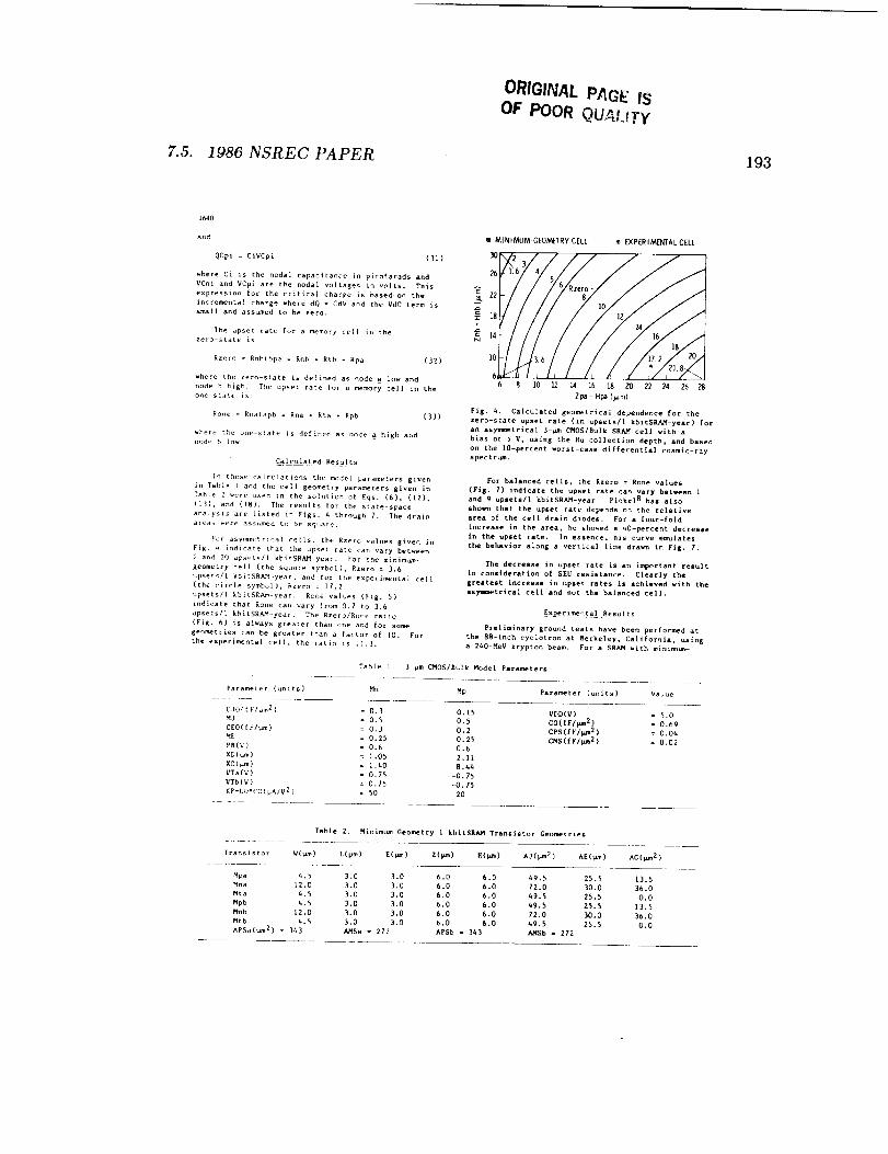
7.5. 1986 NSREC PAPER
ORIGINAL PAGE |S
OF POOR QU4L!Ty
193
1640
and
QCpi = CiYCpi (31)
where Ci is the nodal capacitance in picofarads and
YCni and VCpi are the nodal voltages in volts. This
expression for the critical charge is based on the
incremental charge where dQ = CdV and the VdC term is
small and assuraed to be zero.
The upset tale for a memory cell in the
zero-state is
Bze_o = R_btbpa = Rob *Rtb * Bpa (32)
where the zero_state is defined as node _ low and
node b high. The upset rate for a memory cell in the
one state is:
Rone = gnatapb : Rna + Rta + gpb (33)
where the one state is defined as node a high and
node b low.
C alsulated Results
In these calculations the model parameters given
in Table l and the cell geometry parameters given in
Table 2 were used in the solution of Eqs, (6), ([2),
(i_), and (Ig). The results [or the state-space
analysis are Listed in Figs. 4 through 7, The drain
areas were ass_ed to be square.
For asy_,:trical cells, the Bzero values given in
Fig, _ indicate that the upset rate can vary between
2 and 20 upsets/I kbitSRAN-year. For the minimum-
geometry cell (the square symbol)_ Rzero = 3.6
upset_/l kbitSR&Myear, and for the experimental cell
(the circle symbol), Rzero ; 12.2
upsets/1 kbitS_Am-year. Bone values (Fig. 5)
indicate that gone can vary 6rom 0,7 to 3.6
upsets/1 kbitSRAM--year, The Rzero/Rone ratio
(Fig. 6 ) is always greater than one and for some
geometries can be greater than a factor of lO. For
the experir_ntal cell, the ratio is Li.3.
Table I.
Parameter (_nits} Mn
m MINIMUM-GEOMETRY CELL • EXPERIMENTAL CELL
26 6 4 5
l0 3.6
8 lO 12 14 16 18 2'0 22 24 _ 28
Zpa • Hpa l_m}
Fig. 4. Calculated geometrical dependence for the
zero-state upset rate (in upsets/1 kbitSRAH-year) for
an asy_m_etrical 3-_ CMOS/Bulk SPAN cell with a
bias of 5 V, using the Hu collection depth, and based
on the 10-percent worst-case differential cosmic-ray
spectr_.
For balanced ceils, the Bzero = Bone values
(Fig. 7) indicate the upset rate can vary between I
and 9 upsets/1 kbltSRAH-year. Pickel 8 has also
sho_ that the upset rate depends on the relative
area Of the cell drain diodes, For a four-fold
increase in the area, he showed a 40-percent decrease
in the upset rate. In essence, his curve emulates
the behavior along a vertical line drawn in Fig. 7.
The decrease in upset rate is an important result
In consideration Of SEE resi6tance, Clearly the
greatest Increase in upset fetes is achieved with the
as_lnetrical cell and not the balanced cell.
_rirnental Results
Preliminary ground tests have been performed at
the 8B-inch cyclotron at Berkeley, California, using
a 2hO-MeY krypton beam. For a SRAH with minimum
3-pm CMOS/Bulk Model Parameters
Mp _arame t er (units) Value
CJO(fF/um 2 ) = 0,3 0.15
MJ = 0,5 0.5
CEO(fF/wn) : 0.3 O.2
ME : 0.25 0.25
PB(V) = 0.6 0,6
XD(_) = 1.O5 2.11
XC(um) = 1.40 8.44
VTa(V) = 0.75 -0.75
VTb(V) = 0,25 _0.75
KP=UO*CO(_AIV 2 ) = 50 20
_
VDD(V) = 5.0
CO(fFI_ 2) = 0.69
CPS(fY/l_m 2 ) = 0.04
CMS(fF/Hm 2 ) - 0.02
Table 2. Minimum Geometry l-kbltgRAH Transistor Geometries
Transistor W(pm) L(pm) E(_) Z(_n) H(_) AJ(pm 2 ) AE(_) AC(Bm 2 )
Mpa 4.5 3.0 3.0 6.0 6.0 49.5 25.5 13.5
Mna 12.0 3.0 3.0 6.0 6.0 72.0 30.0 36.O
Mta 4,5 3.0 3,0 6.0 6.0 49.5 25.5 0.0
Mpb 4.5 3.0 3.0 6.0 6.0 69.5 25.5 13.5
Mnb 12.0 3.0 3.0 6.0 6.0 72.0 30.0 3b.0
Mtb 4.5 3.0 3.0 6.0 6.0 _9.5 25.5 0.0
AFSa(_m 2 ) = 343 AHSa = 272 A_Sb = 3t, 3 AHSb = 272
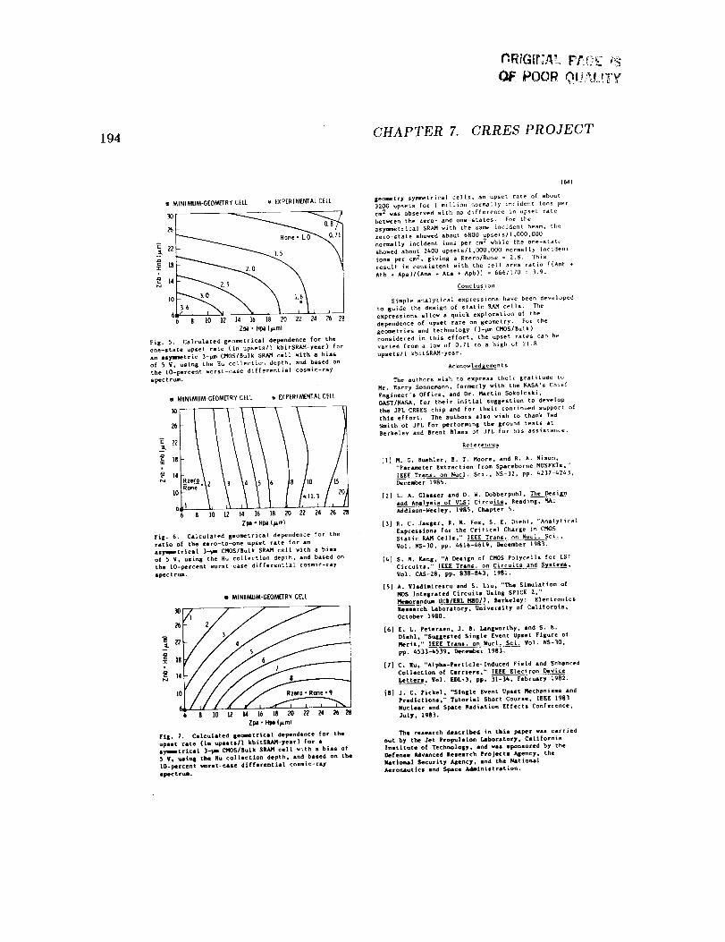
OF POOR qU:_L<T¥
194 CHAPTER 7. CRRES PROJECT
MINIMUM-GEOMETRY CELL _ _PERIh_NTAI CELL
26 0.8
Is- 2.0 l_c 14 2. 5
10 3.0 L6
3.6 •L I
8 10 12 14 16 18 Z0 22 24 26 28
Zpa • Hpa I/_ml
Fig. 5. Calculated geometrical dependence for the
one-state upset rate (in upsets/l kbitSRAM-year) for
an aa]mmetric 3-pm CMOS/Bulk SRAM celI with a bias
Of 5 U. using the Hu collection depth, and based on
the lO-percent worst-case differential cosmic-ray
spectrum.
m MIN_MUM-GEOM_RY CELL _ EXPERIMENTAL CELL
26 -
E 725
N 2 6 8 0
10 - _ll.3
6 L1 l 1
$ 10 [2 ]4 16 18 20 ?Z 24 .?6 ?8
Zpa " Hpe (/_m)
Fig. 6. Calculated geometrical dependence for the
ratio of the zero-to-one upset rate for an
as_trieal 3-pro CMOSlgulk SHAM cell with a bias
of 5 V0 using the Hu collection depth, and based on
the tO-percent worst-case differential cosmiC-ray
spirt rm=.
m MINIMUM-GEOJg_qRY CELL
22 - 4
5
a_
14
10 - Rze_0 • R0ne • 9
$ I0 12 |4 16 Ig 20 T_ 24 26 28
Zpa • Hpa I/_m}
Fig. 7. C_lculated geol_trical dependence for the
upset rate (in upseta/l bbltSRAM-year) for a
syametrical 3-p_ CROS/BuIk ggAR cell with a bias of
5 V, t_llng the gu ¢ollectlot_ depth, and based on the
lO-I_rcent _rlt-Ceae differential cosmic-ray
slmct rum.
1641
geometry symmetrical cells, an upset rate of about
3200 upsets for l million normally i_cident ions per
cm 2 was observed with no dif[erence in upset ra:e
betwten the zero- and one-states. For the
asymmetrical SRAH with the same incident beam, the
zero-state showed about 6800 upsets/[,000,O00
normally incident ions per cm 2 while the one-sea te
_howed about 2400 upsets/l,O00,O00 normally incident
ions per cm 2, giving a Rzero/Rone = 2,8. This
result ia consistent with the cell area ratio [(Anb +
Atb * Apa)/(Ana + Ata * Apb)] _ 656/170 = 3.9.
Conclusion
Simple analytical expressions have been developed
tO guide the design of static P-_ cells. The
expressions allow a quick exploration of the
dependence of upset rate on geometry. For the
geometries and technology (]-pm CMOS/gulk)
considered in this effort, the upset rates can be
varied from a lOW of 0.7[ tO a high of 21.8
upsets/i kbitSRAH-year,
_ements
The authors wish to express their gratitude to
Mr. Barry Sonnemann_ formerly with the NASA's Chief
Engineer's Office, and Dr. Martin Sokoloski,
OAST/NASA, for their initial suggestion to develop
the JPL CRRES chip and for their continued support of
this effort. The authors also wish to thank Ted
Smith of JPL for performing the ground tests at
gerkeley and Erent Bides of JPL for his assistance.
References
Ill M. G* Buehlert S. T, Moore, and R. B. Nixon0
"Parameter Extraction from Spaceborne MOSFETs,"
IEEE _ran_. oo hurl. Sci. NS-}2, pp, h2]_-4243,
December 1985,
121 L. A, Glaszer and D. N. Dobberpuhl, _e_
and Amsl_sis of VL_I Circuit_, Readiog, HA:
Addison-_esley, 1985. Chapter 5.
[3] H. C. Jaeger, g. M, Pox, S. E. Diehl, "Analytical
Expressions for the Critical Charge in CNOS
Static RAM Cells," IEEE Trans. on hurl. Sci,,
Voi. NS-]O, pp. A616-4619, December 1983.
[_] S. N. Kang, "A Design of C_OS Polycells for LSI
Circuits0" IEEE Trans. on Circuits and Systems,
Vol. CAS-28, pp. 838-8h3, 198i.
[5] A. Vladimirescu and S. Liu, "The Simulation of
_OS Integrated Circuits Bsing SPICE 2,"
Nemorandulu UCg/ERL R80/7, _rkeley: Electronics
geseercb Laboratory. University of Califoroia,October 1980.
[6} E. L. Peteraen, J. }. Leng_orthy, and S. E.
Diehl, "S_ggested Single Event Upset Figure of
Merit," IEEE TranL on Nucl. Sci. Vol. NS-30,
pp. k533-_539, December 198].
[71C. gu, "Alpha-Particle-Induced Field and Enhanced
Collection of Carriera,'" IEEE Electron Device
laettera, VoI, EDL-3, pp. 31-34, February 1982.
[8] J. C. Plckel, "Single E_ent Upset Mechanisms and
Predictions," Tutorial Short Course_ IEEE 1983
Nuclear and Space Radiation Effects Conference,
JulT_ 1983.
_e research described in this pa_r wal carried
out by t_Me Jet Propulsion lJboratory. California
l_ltitutl of Technology, and was lpO_lored by the
Defe_le _vanced geselrch Projects klency t the
National Security Agency, and the National
Aerortaut|¢a and Space M_inistration.

7.6. MOSFET MATRIX 195
7.6 MOSFET Matrix
The MOSFET matrix is used for accurate measurement of individually ad-
dressed transistors to allow evaluation of CMOS transistor parameters. Ge-
ometry dependcace of several of these parameters requires MOSFETs with at
least four W/L ratios which, for statistical purposes, are each repeated three or
four times in the matrix.
Two distinct modes of matrix operation are controlled by an enable pin (XT
EN); see Figure 7.15. When XT EN is low, the matrix is in standby and the
transistors are biased in the worst case condition for radiation damage. The
gates of all transistors are connected to VDD (VGS for the n-MOSFET is
5.0V and VGS for the p-MOSFET is 0.0V) and the drains are floated. This
forces radiation-induced positive charge to the silicon dioxide-silicon interface,
where it has the maximum effect on threshold voltage shifts. When the matrix
is enabled, all devices except the device addressed are in a non-conducting state
and transmission gates direct the gate voltage (XT VG) to the transistor under
test. Drain current is forced through a common pin (XT ID) and the drain
voltage (XT VD) is measured by Kelvin connection via transmission gates. A
common p-well connection (XT PWELL) is available for the evaluation of body
effect in n-channel transistors, allowing the well of the transistor under test to
be biased. A common connection to the sources of all p-MOSFET transistors
(XT VPS) is used to evaluate the p-MOSFET body effect. To accomplish this,
VDD, which is tied to chip substrate, is raised above 5 V, while the source is
held at 5 V during the test.
The measurements require an HP4141B, which has four source/monitor
units, two voltage sources, and two voltage monitors; hence the entire measure-
ment can be conducted with one instrument. The matrix addressing circuitry
is powered by chip VDD. The pin assignments for the CRRES chip during and
between irradiation are shown in Section 7.10. The time required for a complete
(ground) test of the matrix is 35 minutes. The measurement configuration in the
MEP is simplified (Figure 7.15) due to limitations on the amount of ancillary
circuitry that can be flown in space.
During the report period, a sample CRRES chip was irradiated using a
Cobalt-60 source. The radiation sequence is shown in Table 7.4. Time between
irradiations was less than 60 minutes. Irradiation, electrical testing, and anneal-
ing were done at room temperature. The chip was mounted in a 64-pin package;
the package lid remained on during irradiation and electrical testing. The elec-
trical data was analyzed with the parameter extraction program, JMOSFIT
[351.
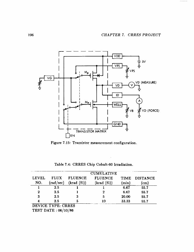
196 CHAPTER 7. CRRES PROJECT
VD (MEASURE)
C_VD (FORCE)
Figure 7.15: Transistor measurement configuration.
Table 7.4: CRRES Chip Cobalt-60 Irradiation.
CUMULATIVE
LEVEL FLUX FLUENCE FLUENCE TIME
NO. (rad/sec) (krad (Si)) (krad (Si)) (min)
DISTANCE
(cm)1 2.5 1 1 6.67
2 2.5 1 2 6.67
3 2.5 3 5 20.00
4 2.5 5 10 33.33
55.7
55.7
55.7
55.7
DEVICE TYPE: CRRES
TEST DATE :06/10/86

7. 7. TIMING SAMPLER 197
All 32 transistors in the matrix were tested between irradiations, and a total
of 252 data points was acquired for each transistor. The gate voltage was steppedfrom 5.0 to 0.25 V in 0.25 V decrements and then to 0.05 V for the final data
point; the drain voltage was stepped from 5.0 to 1.0 V in 0.5 V decrements and
then to 0.6, 0.2, and 0.05 V. Four characteristic transistor curves were plotted
before and after irradiation for each transistor and are shown in Figure 7.16.
The overall chip leakage current is shown versus total Cobalt-60 dose in
Figure 7.17. The leakage current increased from 1 nA at 0 krad(Si) to 8 #A at
10 krad(Si).
Table 7.5 is a row by row comparison of transistors; most parameters are
in close agreement between devices. The parameters with the largest percent
errors are the geometrical coefficients KWG, KWGB, KWD, KWL, HO, and
LO. The primary parameters, such as KP, VTO, and GAMMA agree to within
5 percent.
Tables 7.6 and 7.7 show that the results display the expected behavior for
relatively low radiation doses. That is, the change in the threshold voltage,
VTO, for both n- and p-MOSFETs, indicates a buildup of positive charge in
the oxide. Note that the absolute value of the (negative) threshold voltage is
listed in Table 7.7 for the p-MOSFETs. Parameters expected to be insensitive to
oxide charge are KP, GAMMA, DO, THETA, KLT, RW, EO, KLE, LO, KLL,
and KWL; with the exception of DO and KWL for the n-MOSFETs, this is
evidenced in the results.
Threshold voltage for n- and p-MOSFETs for W/L = 6 lzm/3 lzm are plotted
versus total dose in Figure 7.18. The slope and y-intercept were calculated using
least-squares fitting.
7.7 Timing Sampler
The CRRES Chip timing sampler [2] provides a substantially improved method
for the direct measurement of on-chip circuit delay. The timing sampler is not
afflicted with the problem of higher harmonic oscillation modes, as is the ring
oscillator, since delays are directly measured using externally generated transi-
tions. This results in repeatable and accurate measurements, and therefore, a
high degree of confidence in the results.

198 CHAPTER 7. CRRES PROJECT
363
303
242
>
>182
<
= 121
0.O0 1.OO 200 3.00 400 5.00
VG(V)
000 I 00 200 300 400 5 00
VGIV)
VD=VO = 23.0 5 O0
o.o5 ,-/_.,,i ._//.,,_ 4:5o
020 !-0.60 192350
1.oo I ,4V/ ..,I"3 3001.5o 154 I- _F"_ -1 25o2.5o2°°_ I j-/ _ 2.00300 ,151_ i t,:'o°3.50 -_ I J'/ I o.6o4.00
O0000 1 O0 200 3 O0 4 O0 5.00
VG(V)VG
VD= 531 5.005.00 4.75
450 4.50
400 443 4.254.O0
3.50 3.75
3.00 354 3.50250 3.25
3002.00 A275
1,50 _.266 2.50I O0 2.25
060 2001,75
020 177 1.50005 1.25
1.00
89 0.750.500.25
0 0.05
000 1 O0 2.00 3 O0 400 500
VD(Vl
;Oo =372 5 ' 5.00
I /JA 0.20 45031oF ///I o.6o . 4.00
I ////I 1oo 35oI ////j 15o 300
>- I /II//A 2.50 200
>0186L "/////_3"00 _ r f_ 1 1"50r j-//////_ 350 122 1ooI /////////_ 4.00 o.eo
= I-124 //////,'/._=_=_ 4 5os oo "62 r .,_,.._..._..__ o.2ooos
.___ 0,00 1 O0 200 3.00 4.00 5.00 0.00 I O0 200 300 400 5.00MG(VI VGMG(V) VD = 584 5.00
30 l I I _ 5.00 4.75
450 4.50
4.00 467 4.25" 4.00
4.0 3.50 3.75= 3.00 3.50
_._ _ 250 389 3.25¢ z 5.0 200 3.00
:ED< _ - 2,75¢ 150 .._ 292 2.501 O0 2.25
"_ 6.0 060 2.001.75
0,20 135 1.500.05 1 25
1.00
T 7.0 -- 97 0.750.50
0.25
80 I I t t 0 0.050.00 1.00 2.00 3.00 4.0o 5o0 0.00 100 2.0o 3.00 4.0o 5.0o
VGIV) VD(VI
Figure 7.16: n-Channel MOSFET pre-irradiation curves (top) and post-irradia-
tion curves (bottom) after 10 krad(Si) at 2.5 rad(Si)/sec).

7. 7. TIMING SAMPLER 199
IOOuA
10. uA
i.0uA
100hA
tO. nA
i.0nA
0.InA
I I I I I I I | | I I
PRERAD
_DOSE RATE =
, CHIP 1
2.5 Rad
, i l , I i l _ i I ,
1.0 I0
DOSE C0-60, kRAD (Si)
Figure 7.17: CRRES Chip leakage versus total dose.
Si)/s
I
I00
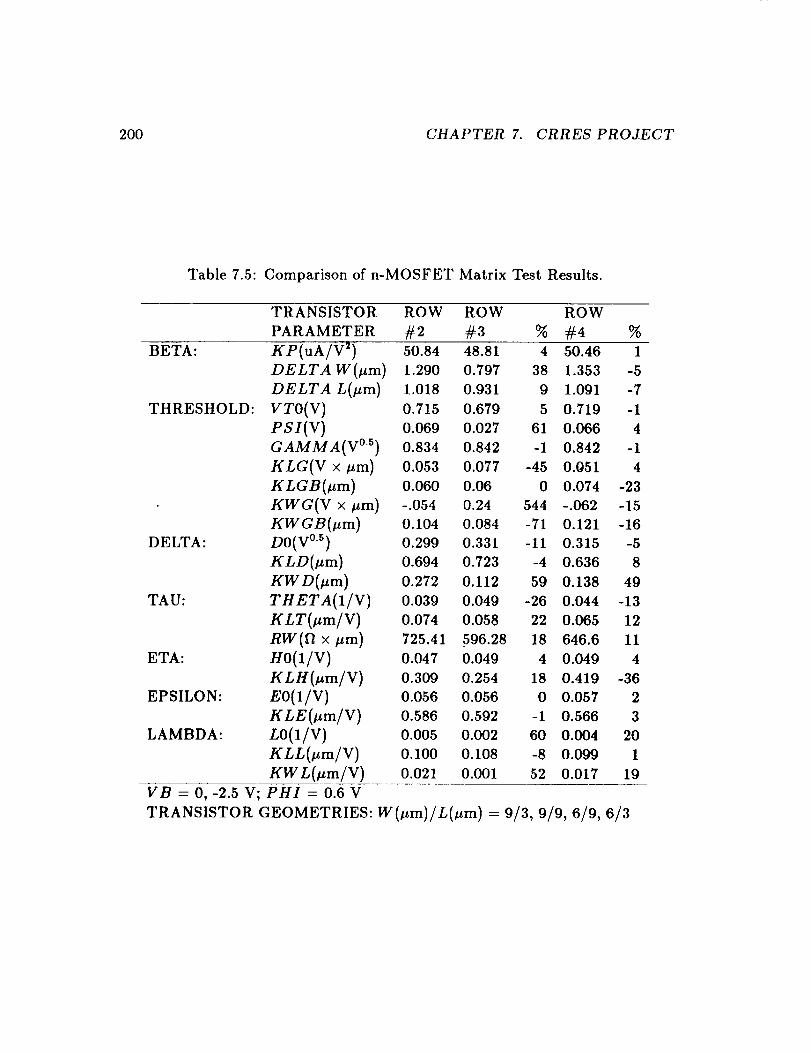
200 CHAPTER 7. CRRES PROJECT
Table 7.5: Comparison of n-MOSFET Matrix Test Results.
TRANSISTOR ROW ROW ROW
PARAMETER #2 #3 % #4 %
BETA: KP(uA/V 2) 50.84 48.81 4 50.46 1
DELTA W(#m) 1.290 0.797 38 1.353 -5
DELTA L(_m) 1.018 0.931 9 1.091 -7
THRESHOLD: VT0(V) 0.715 0.679 5 0.719 -1
PSI(V) 0.069 0.027 61 0.066 4
GAMMA(V °s) 0.834 0.842 -1 0.842 -1
KLG(V × #m) 0.053 0.077 -45 0.051 4
KLGB(#m) 0.060 0.06 0 0.074 -23
KWG(V x #m) -.054 0.24 544 -.062 -15
KWGB(Izm) 0.104 0.084 -71 0.121 -16
DELTA: D0(V °'s) 0.299 0.331 -11 0.315 -5
KLD(I_m) 0.694 0.723 -4 0.636 8
KWD(#m) 0.272 0.112 59 0.138 49
TAU: THETA(1/V) 0.039 0.049 -26 0.044 -13
KLT(#m/V) 0.074 0.058 22 0.065 12
RW(_ x _um) 725.41 596.28 18 646.6 11
ETA: H0(1/V) 0.047 0.049 4 0.049 4
KLH(t_m/V) 0.309 0.254 18 0.419 -36
EPSILON: E0(1/V) 0.056 0.056 0 0.057 2
KLE(I_m/V) 0.586 0.592 -1 0.566 3
LAMBDA: L0(1/V) 0.005 0.002 60 0.004 20
KLL(_m/V) 0.100 0.108 -8 0.099 1
KWL(#m/V) 0.021 0.001 52 0.017 19
VB = O,-2.5 V; PHI = 0.6 V
TRANSISTOR GEOMETRIES: W(#m)/L(lzm) = 9/3, 9/9, 6/9, 6/3

7. 7. TIMING SAMPLER 201
Table 7.6: n-MOSFET Matrix Cobalt-60 Radiation Test Results.
TRANSISTOR TOTAL DOSE (krad (Si))
PARAMETER Ok lk % 5k % 10k
- BE]-TA: gb{UA/V:_i 50.84 49.54 3 53.40 -5 49.23
DELTA W(#m) 1.290 1.049 19 1.437 -11 1.002
DELTA L(#m) 1.018 1.054 -4 0.998 2 0.996
THRESHOLD: VT0(V) 0.715 0.681 5 0.612 14 0.421
PSI(V) 0.069 0.033 52 -.031 145 -.287
GAMMA(V °5) 0.834 0.837 -4 0.83 5 0.914
KLG(V × #m) 0.053 0.049 8 0.071 -34 -.028
KLGB(#m) 0.060 0.074 -23 0.067 -12 0.126
KWG(V x #m) -.054 -.045 -17 -.216 300 -.301
KWGB(#m} 0.104 0.133 -28 0.1 4 0.114
DELTA: D0(V °s) 0.299 0.3 0 0.33 -10 0.426
KLD(#m) 0.694 0.635 9 0.744 -7 0.926
KWD(pm) 0.272 0.388 -43 0.248 9 0.245
TAU: THETA(1/V) 0.039 0.035 10 0.045 -15 0.04
KLT(#m/V) 0.074 0.081 -10 0.062 16 0.07
RW(i2 x #m) 725.41 813.2 -12 579.25 20 707.2
ETA: H0(1/V) 0.047 0.105 -123 0.106 -126 0.206
KLH(#m/V) 0.309 0.528 -71 0.341 -10 0.194
EPSILON: E0(1/V) 0.056 0.051 9 0.057 -2 0.058
KLE(#m/V) 0.586 0.596 -2 0.593 -1 0.603
LAMBDA: L0(1/V) 0.005 0.003 40 0.005 0 0.005
KLL{#m/V) 0.100 0.098 2 0.103 -3 0.103
KWL(#m/V) 0.021 0.001 52 0.019 10 0.012
%3
22
2
41
516
-10
153
-110
457
-10
-43
-33
10
-3
5
3
-338
37
-4
-3
0
-3
43
VB = 0,-2.5 V; PHI = 0.6 V
TRANSISTOR GEOMETRIES: W(#m)/L(l_m) = 9/3, 9/9, 6/9, 6/3

202 CHAPTER 7. CRRES PROJECT
Table 7.7: p-MOSFET Matrix Cobalt-60 Radiation Test Results.
TRANSISTOR TOTAL DOSE (krad (Si))PARAMETER Ok lk % 2k % 5k %
BETA: KP-(u-A/V_i 18.03 18.61 -3 18.41 -2 17.23 4
DELTA W{#m) 0.527 1.075 -104 0.898 -71 0.835 -58
DELTA L(#m) 1.112 1.026 8 1.082 3 1.209 -9
THRESHOLD: VT0{V) 0.776 0.809 -4 0.835 -8 0.893 -15
PSI(V) 0.425 0.462 -9 0.502 -18 0.541 -27
GAMMA(V °5) 0.453 0.448 1 0.431 5 0.455 -0.4
KLG(V x pro} 0.081 0.087 -7 0.067 17 0.052 36
KLGB(#m) 0.117 0.108 8 0.108 8 0.098 16
KWG(V × pro) 0.159 0.163 -3 0.189 -19 0.358 -125
KWGB(#m) 0.104 0.094 10 0.122 -17 0.073 30
DELTA: D0(V °'5} 0.25 0.204 18 0.230 8 0.201 20
KLD(pm) 0.428 0.482 -13 0.414 3 0.215 50
KWD(#m) 0.425 0.116 73 0.009 98 -.191 145
TAU: THETA(I/V) 0.099 0.106 -7 0.113 -14 0.I03 -4
KLT(#m/V) 0.073 0.047 36 0.049 33 0.053 27
RW(fl x #m) 2038 1270 38 1323 35 1551 24
ETA: HO(I/V} 0.47 0.198 58 0.258 45 0.1 79KLH(#m/V) 0.845 0.625 26 0.741 12 1.326 -57
EPSILON: E0(1/V) 0.043 0.043 0 0.036 16 0.034 21
KLE(pm/V) 0.313 0.283 10 0.268 14 0.273 13
LAMBDA: L0{1/V) 0.018 0.014 22 0.013 28 0.016 11
KLL(pm/V) 0.174 0.187 -7 0.184 -6 0.174 0
KWL{pm/V} 0.039 0.037 5 0.028 28 0.032 18
VB = O,2.5 V; PHI = 0.6 VTRANSISTORGEOMETRIES:W(#m)/L(pm) = 9/3, 9/9, 6/9, 6/3

7. 7. TIMING SAMPLER 203
1.8 -- [] :VBS=0, SLOPE_-30.0 mV/kRAD (Si), VTo-0.674V
1 6 _-- O :VBS=-2.5, SLOPE=-30.9 mV/kRAD (Si], VTo_=1.47V
1 4(_ _ DOSE RATE= 2.5 RAD(Si)/S --
• ._ _ VTI2, CHIP#l, W = 6#tm, L=3k(rr, :
_" 1.2 _-_--- _]_.,_-CHANNEL MOSFET -_
,.o--_-0.8 -- -=
0.6(_
o.4
o __,,, 1,,,,1,,,,i,,,,i,,,, i,,,,i,_f,l,l_,l,l,,ll,,,_-0.2 --
- [] :VBS--0 SLOPE=-34.7 mV/kRAD(Si), VTo=-0.762V -
-0.4 -__-- O:VBS:2.5 SLOPE=-34.5 mV/kRAD(Si), VT o :-1.11V --
-o._--0.8 [_ DOSE RATE : 2.5 RAD(Si)Is --
Z '-'__.._.._ VTI2, CHIP#l,, W:6_,lm, L=3/_m -
-1_0(__ _ P-CHANNEL MOSFET --_,._-_--_ __ _ -_
-1.6
-1.8 _ __ :
-2.o ,,, I,,,,I,JJ , I,,_,1,,,, I,,,,1 ,,,,1_,,, h-_,, I,,,,-0 3 6 9 12 15 18 21 24 27 30
DOSE Co-60 (KRAD)
Figure 7.18: Threshold voltage versus dose for n- (top) and p-channel (bottom)
MOSFETs. The gate voltage was 5 V during irradiation.

204 CHAPTER 7. CRRES PROJECT
7.7.1 Test Hardware and Measurement Procedure
The CRRES chip timing sampler array consists of a series of 128 identical invert-
ers grouped as 64 inverter-pairs. The output of each inverter-pair is connected
to one input of a dynamic Muller-C timing sampler element. The other input of
each timing sampler element is connected to the timing sampler array's enable
input pad (TSE). The input to the first inverter-pair of the chain is connected to
the timing sampler array's delay chain input pad (TSI). As a result of space and
weight limitations, the measurement procedure on the CRRES satellite consists
of applying a fixed 100 ns delay input (delay between edges on TSI and TSE
pins), and then reading the 6-bit binary output word. This output word reflects
the number of inverter-pairs the transition has propagated through in the 100
ns period. The timing sampler is essentially a delay-to-digital converter, and
therefore results in a possible quantization error in the measured output. This
error is minus one least significant bit and results in a worst-case inverter-pair
delay error of 100/N percent where N is the number of inverter pairs tripped.
The wafer level measurements performed in the JPL VLSI technology lab
employ a more sophisticated technique which eliminates this quantization error
and allows the delay to be measured at each of the 64 taps on the inverter-pair
chain. The delay from TSI input to tap N on the inverter-pair chain is measured
by applying a start transition to input TSI followed by a stop transition on
TSE, and then observing the circuit output D0-D5. This sequence is repeated
at a 100 kHz rate by a tester that adjusts the delay between start and stop
transitions each cycle. The delay is increased when the output from the previous
cycle is less than N and decreased when the output is greater than or equal
to N. Figure 7.19 illustrates the measurement timing relationships. When the
TSI (START)
TSE (STOP)
OUT ) N
h
I I
I I
I
I
I
ARM INPUTDELAY # 2
I I I IRESET I ARM INPUT DATA REST I DATA J
VALID I ] VALID II DELAY#1 ] (OUT<N) II I (OUT _= N)I
i I I i Ii I
_, 10 ,us CYCLE # 1 _i _ 10 ,us CYCLE # 2 _'_
Figure 7.19: Timing analysis for the CRRES chip timing sampler.
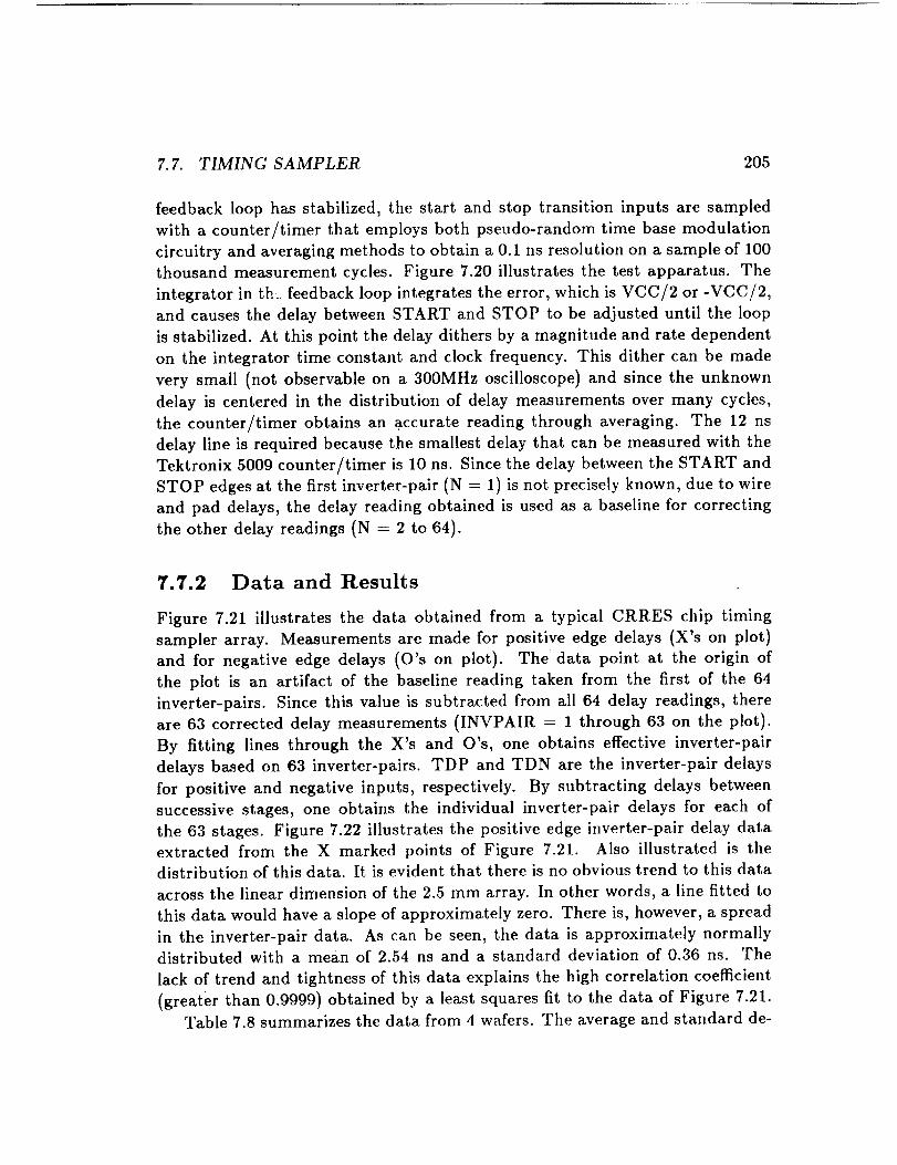
7. 7. TIMING SAMPLER 205
feedback loop has stabilized, the start and stop transition inputs are sampled
with a counter/timer that employs both pseudo-random time base modulation
circuitry and averaging methods to obtain a 0.1 ns resolution on a sample of 100
thousand measurement cycles. Figure 7.20 illustrates the test apparatus. The
integrator in th_ feedback loop integrates the error, which is VCC/2 or -VCC/2,
and causes the delay between START and STOP to be adjusted until the loop
is stabilized. At this point the delay dithers by a magnitude and rate dependent
on the integrator time constant and clock frequency. This dither can be made
very small (not observable on a 300MHz oscilloscope) and since the unknown
delay is centered in the distribution of delay measurements over many cycles,
the counter/timer obtains an accurate reading through averaging. The 12 ns
delay line is required because the smallest delay that can be measured with the
Tektronix 5009 counter/timer is 10 ns. Since the delay between the START and
STOP edges at the first inverter-pair (N = 1) is not precisely known, due to wire
and pad delays, the delay reading obtained is used as a baseline for correcting
the other delay readings (N = 2 to 64).
7.7.2 Data and Results
Figure 7.21 illustrates the data obtained from a typical CRRES chip timing
sampler array. Measurements are made for positive edge delays (X's on plot)
and for negative edge delays (O's on plot). The data point at the origin of
the plot is an artifact of the baseline reading taken from the first of the 64
inverter-pairs. Since this value is subtracted from all 64 delay readings, there
are 63 corrected delay measurements (INVPAIR = 1 through 63 on the plot).
By fitting lines through the X's and O's, one obtains effective inverter-pair
delays based on 63 inverter-pairs. TDP and TDN are the inverter-pair delays
for positive and negative inputs, respectively. By subtracting delays between
successive stages, one obtains the individual inverter-pair delays for each of
the 63 stages. Figure 7.22 illustrates the positive edge inverter-pair delay data
extracted from the X marked points of Figure 7.21. Also illustrated is the
distribution of this data. It is evident that there is no obvious trend to this data
across the linear dimension of the 2.5 mm array. In other words, a line fitted to
this data would have a slope of approximately zero. There is, however, a spread
in the inverter-pair data. As can be seen, the data is approximately normally
distributed with a mean of 2.54 ns and a standard deviation of 0.36 ns. The
lack of trend and tightness of this data explains the high correlation coefficient
(greater than 0.9999) obtained by a least squares fit to the data of Figure 7.21.
Table 7.8 summarizes the data from 4 wafers. The average and standard de-

206 CHAPTER 7. CRRES PROJECT
DEC LSI 11/73 ISYSTEMCONTROLLER
I!
IEEE488 IB
TEKTRONIX 5009
COUNTER/TIMER
(1
CRRES CHIPTIMINGSAMPLER ARRAY
TSI TSE
START STOP
12nsDELAY
DO° /6• I
D5
TIMING WAVEFORM GENERATOR
IVCC
IIIIII[
VCC
I
D
VOLTAGEICONTROLLED
: DELAY JGENERATOR
I
J
A
A>B
B
FEEDBACK
Figure 7.20: Apparatus for measuring JPL CRRES chip timing sampler.

7. 7. TIMING SAMPLER 207
180-
160-
140-
C
= 1204--*
r-,.-
0100
5 8o
"' 60._J"-n
40
20
0
VDD : 5 VOLTS, VT12 CHIP #2lllhl II I h I11, h III I h I IIIh I IIIIIhh Ill III I II I h l lit III Ih I, I,I Ill Ill I II I II I|1 I Jllh I II I I1 I II I hill I hh h | II * II I Ill III ,I ,.1,
X : POSITIVE INPUT EDGE (tn) >"_,_<I_E-
0 = NEGATIVE INPUTEDGE(tn) _/ I
__J_ .
MEP DELAY RANGE _;_g_;_";"
-7-
J TDP lp/Np 2.95 ns
TDN -tn/N n :2.82ns
,,i, n" l,U, I' l,l, l, i ,], n,l ,l' U'l 'l, l 'I, I, I,I ,u, T,l, 1, I,I, I, 1,1, l, i ,i, l, |,l, I, +,I, i, l ,u, l'n' I ' I, I,I, l" I 'T" l,r, i, I 'i" I' i'i, 1+ v ,it+
0 5 lO 15 20 25 30 35 40 45 50 55 60
NUMBER OF INVERTER PAIRS TRIPPED, Nn OR Np
Figure 7.21: Timing sampler inverter-pair array data.

208 CHAPTER 7. CRRES PROJECT
3.6
3.4
3.2
3.0u')
¢-
"-'2.8>-
w 2.6r%
2.4<
_ 2.2
,,, 2.0>_- 1.8
" 1.6
1.4
I I I I I I
I I I I I I I I
5 10 15 20 25 30 35 40
INVERTER PAIR NUMBER
I I I I t
I
I I 1 I_
45 50 55 60
I t
1.0 2.0
DISTANCE ACROSS INVERTER PAIR ARRAY (ram)
!2.5
INTERVAL NO.
MIDPOINT OBS.
(ns)
1.35 1
1.47 1
1.58 1
1.70 0
1.81 1
1.93 0
2.04 0
2.16 - 3
2.27 2
2.39 10
2.50 > 13
2 .62 13
2.73 4
2.85 + 9
2.96
3.08
3.19
3.31
3.42
3.54
MEAN STDEV
2.53 ns 0.360 ns
Figure 7.22: Positive edge
NUMBER OF OBSERVATIONS
0 i0 20
+ ......... + ......... +
2
i
0
I *
0
1 *
**********
*************
*************
*********
% STDEV MEDIAN MINIMUM MAXIMUM
14.1 2.50 ns 1.30 ns 3.60 ns
inverter-pair delta data from one chip.

7. 7. TIMING SAMPLER 209
Table 7.8: Summarized data from the timing samplers on four wafers.
Wafer #1 (9 sites tested)'EAN STDEV % STDEV MEDIAN MINIMUM MAXIMUM
TDP 2.72 0.113 4.16 2.71 2.57 2.86
PR2 0.9998 0 0 0.9999 0.9995 0.9999
TDN 2.57 0.102 3.97 2.58 2.42 2.69
NR2 0.9999 0 0 0.9999 0.9998 0.9999TDPAVG 2.69 0.107 3.97 2.68 2.54 2.83
TDPSIG 0.27 0.03 11.0 0.28 0.22 0.31
TDNAVG 2.56 0.104 4.05 2.56 2.41 2.68
TDNSIG 0.20 0.03 " 15.3 0.19 0.15 0.25
Wafer #4 (41 sites tested)MEAN STDEV _ STDEV MEDIAN MINIMUM MAXIMUM
TDP 2.61 0.158 6.05 2.61 2.29 2.94
PR2 0.9999 0 0 0.9999 0.9997 0.9999
TDN 2.46 0.134 5.43 2.46 2.18 2.73
NR2 0.9999 0.0006 0.062 0.9999 0.9995 0.9999
TDPAVG 2.58 0.159 6.16 2.59 2.26 2.92
TDPSIG 0.26 0.03 13.3 0.26 0.15 0.32
TDNAVG 2.44 0.135 5.54 2.45 2.14 2.71
TDNSIG 0.20 0.04 20.0 0.20 0.13 0.28
Wafer #5 (70 sites tested)MEAN STDEV % STDEV MEDIAN MINIMUM MAXIMUM
TDP 2.65 0.179 6.76 2.65 2.31 3.64
PR2 0.9999 0 0 0.9999 0.9997 0.9999TDN 2.48 0.27 11.04 2.51 0.56 3.22
NR2 0.9999 0.0005 0.047 0.9999 0.9993 0.9999
TDPAVG 2.62 0.173 6.59 2.62 2.29 3.54
TDPSIG 0.28 0.05 17.1 0.27 0.22 0.61
TDNAVG 2.49 0.141 5.68 2.50 2.21 3.15TDNSIG 0.19 0.05 27.6 0.19 0.10 0.56
Wafer #10 (9 sites tested)MEAN STDEV % STDEV MEDIAN MINIMUM MAXIMUM
TDP 2.80 0.131 4.70 2.81 2.56 3.02
PR2 0.9999 0 0 0.9999 0.9998 0.9999
TDN 2.66 0.126 4.75 2.67 2.43 2.87
NR2 0.9999 0 0 0.9999 0.9998 0.9999
TDPAVG 2.76 0.127 4.59 2.76 2.53 2.98
TDPSIG 0.27 0.04 14.8 0.26 0.22 0.34TDNAVG 2.65 0.119 4.51 2.64 2.43 2.85
TDNSIG 0.18 0.02 10.8 0.19 0.15 0.21

210 CHAPTER 7. CRRES PROJECT
viation computed from the inverter-pair data for positive/negative input transi-
tions is specified by TDPAVG/TDNAVG and TDPSIG/TDNSIG, respectively.
PR2/NR2 are the correlation coefficients corresponding to the line fits for the
positive/negative transition data. Notice that the average delay variation over
a wafer is very small, with a standard deviation of less than 0.2 ns.
The inverter-pair delays for positive and negative transitions on wafer #4
are displayed in Figures 7.23 and 7.24 respectively. The 41 boxed numbers are
the actual locations that were measured on this wafer. These maps show that
the fastest circuits would be obtained from the lower left side on the wafer.
If a microprocessor, whose longest computational delay per clock cycle was 80
gate delays, was fabricated on this run, processors from the lower left portion
of the wafer could run at a maximum clock frequency of around 11.5 MHz but
processors from the upper right portion of the wafer could run only 9 MHz.
The inverter-pair delay for positive transitions is 5 to 6 percent larger than
the inverter-pair delay for negative transitions. This difference is due to the
different response times of the n- and p-channel transistors in the inverters.
This is due to the timing sampler's design in which the first inverter of each
inverter-pair drives a fanout of 1 and the second inverter drives a fanout of 2.
So, if the input to the inverter pair is a positive edge, the n-channel transistor in
the first inverter drives the output (fanout of 1) while the p-channel transistor
in the second inverter drives the output (fanout of 2). If these fanouts were
the same, then the positive and negative transition delays would be equal. The
magnitude of the delay difference between positive and negative transition delays
is a function of the loading imbalance as well as the p=channel and n-channel
transistor channel mobility difference and the ratio of the p-channel to n-channel
width to length ratio r (r = 5/3 on CRRES chip). This inverter-pair delay can
be expressed in terms of intrinsic n-channel and p-channel transistor delays Tn
and vp respectively [2].
7.7.3 Conclusions
The data obtained from the CRRES chip timing sampler demonstrates this
approach to be accurate and robust. This structure provides an easy way to
measure inverter delays on a satellite that has power and weight limitations and
cannot afford to include standard type lab test equipment such as a frequency
counter. Since the delay data obtained from one timing sampler array shows that
the inverter pairs all have the same delay (±0.4ns), the procedure performed on
the satellite (inverter-pair delay = 100 ns/# stages tripped) should give accurate
results to within minus one least significant bit.

ORIGINAL PAGE IS
OF POOR QUALITY
7. 7. TIMING SAMPLER 211
12 v
ii v
I0 v
9 v
8 v
7 v
6 v
5 V
4 v
3 v
2 v
1
>< >< >< >< >< >< >< >< >< >< ><
1 3 5 7 9 ii
2 4 6 8 i0 12
-: less than 2.25 ns
0:2.25 ns to 2.32 ns
i: 2.32 ns to 2.39 ns
2:2.39 ns to 2.45 ns
3:2.45 ns to 2.52 ns
4:2.52 ns to 2.59 ns
5:2.59 ns to 2.65 ns
6:2.65 ns to 2.72 ns
7: 2.72 ns to 2.78 ns
8:2.78 ns to 2.85 ns
9: 2.85 ns to 2.92 ns
+: 2.92 ns or greater
INTERVAL NO.MIDPOINT OBS.
(ns)
2 29 4
2 35 1
2 42 - 4
2 49 3
2 55 > 9
2 62 9
2 69 4
2.75 + 3
2.82 3
2.88 1
NUMBER OF OBSERVATIONS
0 i0 20
+ ......... + ......... +
***
MEAN STDEV % STDEV MEDIAN MINIMUM MAXIMUM
2.57 ns 0.159 ns 6.15 2.58 ns 2.25 ns 2.92 ns
Figure 7.23: Wafer map of the average inverter-pair delay for positive edges
(Wafer 4).

ORIGINA[ PAGE' iS
OF POOR QUALITY
212 CHAPTER 7. CRRES PROJECT
>< >< >< >< >< >< >< >< >< >< ><
12
ii
I0
9
8
7
6
5
4
3
2
1
v
9 ^V
A
V
A
V
4 ^
V
^
V 4
0 ^
v
01 ^
v 9A
V
001 ^
V
3 ^V
)- ^
>< >< >< >< >< >< >< >< >< >< ><
1 3 5 7 9 ii
2 4 6 8 i0 12
-: less
0:2.13
i: 2.19
2:2.25
3:2.30
4:2.36
5:2.42
6:2.48
7:2.53
8:2.59
9:2.65
+: 2.71
than
ns tons to
ns to
ns to
ns to
ns to
ns tons to
ns to
ns to
_s or
2 13 ns
2 19 ns
2 25 ns
2 30 ns
2 36 ns
2 42 ns
2 48 ns
2 53 ns
2 59 ns
2 65 ns
2 71 ns
greater
INTERVAL NO. NUMBER OF OBSERVATIONS
MIDPOINT OBS.
(ns) 0 i0 20+ ......... + ......... +
2.16 2 **
2.22 3 ***
2.27 - 3 ***
2.33 2 **
2.39 5 *****
2.45 > 11 ***********
2.50 6 ******
2.56 + 4 ****
2.62 2 **
2.68 3 ***
MEAN STDEV % STDEV MEDIAN MINIMUM MAXIMUM
2.44 ns 0.135 ns 5.54 2.45 ns 2.13 ns 2.71 ns
Figure 7.24:
(Wafer 4).
Wafer map of the average inverter-pair delay for negative edges

7.8. CONCLUSIONS 213
7.8 Conclusions
The major goal of the JPL CRRES chip project was to provide parts to AFGL
for inclusion on the MEP. This was accomplished in March 1986. Additional,
parts have been J_elivered to the ground test part of the CRRES program.
In this report period, the SRAM design was changed in two important ways:
design rule violations were eliminated and the asymmetrical SRAM cell design
was incorporated to increase the overall probability of seeing SEU. Results from
SEU tests of the asymmetrical cell indicate that the upset rate is almost a factor
of three greater than that of the balanced cell. Since these tests were performed
at energy levels substantially above the minimum energy required to cause upset,
the results correspond to the cr0ss-section ratio between the cell geometries.
The transistor matrix design has not changed in the report period except for
a slight modification in the ancillary circuitry mandated by foundry-specified
minimum design spacings. Results from electrical tests confirm that transistor
parameters extracted from transistors in an addressed matrix are a highly suc-
cessful and preferable alternative to testing individual transistors. Cobalt-60
test results indicate the decoder circuitry does not interfere in any way with
transistor measurements until a sufficiently high dose causes the n-channel en-
hancement mode devices to become depletion mode.
7.9 Future Work
The functions of the CRRES chip will be split into two chips, an SEU Chip and
a TID Chip. This is being done since many SRAMs are needed in a satellite
experiment in order to get sufficient statistical data on SEUs. For the CRRES
chip SRAM cell, we calculate 10 Mbits would be desired. The TID Chip will
consist of a MOSFET matrix and timing sampler.
Experimental work is planned to study the radiation effects of the field-oxide
devices on MOSFET matrix measurements to establish the specific cause of chip
leakage currents. This work is essential to evaluate potential design changes.
Plans for upgrading functional test capabilities are underway. Improved test
capabilities will greatly simplify and expedite heavy ion testing of the SRAM
and Cobalt 60 testing of the MOSFET matrix and timing sampler.

214 CHAPTER 7. CRRES PROJECT
7.10 CRRES Chip Test Configuration Pin Outs
This section contains pin-outs and connection diagrams to serve as a guide to a
user of the JPL CRRES chip.
1. CRRES Chip Leakage Measurement Pin Configuration
PIN FUNCTION PIN STATE PIN FUNCTION PIN STATE
1 VDD VDD 33 SRAM DQ12 GND
2 XT VPS VDD 34 SRAM DQ11 GND
3 SRAM A7 GND 35 SRAM DQ10 GND
4 XT VG GND 36 SRAM DQ9 GND
5 INV OUT NC 37 SRAM DQ8 GND
6 INV SUB VDD 38 SRAM DQ7 GND
7 INV VDD VDD 39 SRAM DQ6 GND
8 INV p-GATE GND 40 SRAM DQ5 GND
9 INV VSS GND 41 SRAM DQ4 GND
10 INV WELL GND 42 SRAM DQ3 GND
11 XT WELL GND 43 SRAM DQ2 GND
12 INV n-GATE GND 44 SRAM DQ1 GND
13 SPARE GND 45 SRAM DQ0 GND
14 SPARE GND 46 SRAM S GND
15 TS I GND 47 SRAM W GND
16 TS E GND 48 SRAM E GND
17 SPARE GND 49 SRAM EP GND
18 SPARE GND 50 SRAM A5 GND
19 SPARE GND 51 SRAM A4 GND
20 SPARE GND 52 SRAM A3 GND
21 SPARE GND 53 SRAM A2 GND
22 SPARE GND 54 SRAM A1 GND
23 TS DO NC 55 SRAM A0 GND24 TS D1 NC 56 XT EN GND
25 TS D2 NC 57 SRAM A6 GND
26 TS D3 NC 58 XT R1 GND
27 TS D4 NC 59 XT R0 GND
28 TS D5 NC 60 XT CO GND
29 GND GND 61 XT C1 GND
30 SRAM DQ15 GND 62 XT C2 GND
31 SRAM DQ14 GND 63 XT ID NC
32 SRAM DQ13 GND 64 XT VD NCNC = NO CONNECTION
TS = TIMING SAMPLER
XT = TRANSISTOR MATRIX
SRAM = STATIC RANDOM ACCESS MEMORY
INV = INVERTER

7.10. CRRES CHIP TEST CONFIGURATION PIN OUTS 215
2. CRRES Chip Pin Configuration for SRAM Operation. See also Fig-
ures 7.1, 7.3, and 7.25.
PIN FUNCTION PIN STATE PIN FUNCTION PIN STATE
1 VDD VDD 33 SRAM DQ12 (0,I)
2 XT VPS VDD 34 SRAM DQII (0,I)
3 SPARE GND 35 SRAM DQI0 (0,I)
4 XT VG GND 36 SRAM DQ9 (0,1)
5 INV OUT NC 37 SRAM DQ8 (0,I)
6 INV SUB VDD 38 SRAM DQ7 (0,I)
7 INV VDD VDD 39 SRAM DQ6 (0,I)
8 INV p-GATE GND 40 SRAM DQ5 (0,I)
9 INV VSS GND 41 SRAM DQ4 (0,I)
10 INV WELL GND 42 SRAM DQ3 (0,1)
11 XTWELL GND 43 SRAM DQ2 (0,1)
12 INV n-GATE GND 44 SRAM DQ1 (0,1)
13 SPARE GND 45 SRAM DQ0 (0,1)
14 SPARE GND *46 SRAMS *(0,1)
15 TS I GND *47 SRAM W *(0,1)16 TS E GND *48 SRAM E *(0,1)
17 SPARE GND *49 SRAM EP *(0,1)
18 SPARE GND 50 SRAM A5 (0,1)
19 SPARE GND 51 SRAM A4 (0,1)
20 SPARE GND 52 SRAM A3 (0,1)
21 SPARE GND 53 SRAM A2 (0,1)
22 SPARE GND 54 SRAM A1 (0,1)
23 TS DO NC 55 SRAM A0 (0,1)24 TS D1 NC 56 XT EN GND
25 TS D2 NO 57 SPARE GND
26 TS D3 NO 58 XT R1 GND
27 TS D4 NC 59 XT R0 GND28 TS D5 NC 60 XT CO GND
29 GND GND 61 XTC1 GND
30 SRAM DQI5 (0,1) 62 XT C2 GND
31 SRAMDQ14 (0,1) 63 XT ID NC
32 SRAM DQ13 (0,1) 64 XT VD NCNC = NO CONNECTION
TS = TIMING SAMPLER
XT = TRANSISTOR MATRIX
SRAM = STATIC RANDOM ACCESS MEMORY
INV = INVERTER
*SRAM S, SRAM W, SRAM E, AND SRAM EP, SEE TIMING DIAGRAM

ORIGINAL PAGE IS
OF POOR QUALITY
216 CHAPTER 7. CRRES PROJECT
BLOCK DIAGRAM:
AO 55 0-,,-_A1 ._ e,---
,_ S2 _"--
A5 50 _"--AS 57 _
A7 3 _'-'-_
! LLJ
44 DQ1
31 DQ14
IO_30 DO15
,11 2tl 48474849
VDD GND S W E EP
TIMING DIAGRAM:
S
w_--_
EP
READ CYCLE
/
I.,,--• --,,_,_-----".-_,,._-. ,:-,,.l
_._ d_'
P-XT ON
N-XT OFF
TG OFF
B OFF
A_
SPECIFICATIONS:
\ ore /
/ ON
OTHER PINS IN
STANDBY CONDITION
WRITE CYCLE
w x_L/ __
ON
P-XT _ OFF
OFF N-XT OFF _ OFF
TG OFF
f ON _ B OFF
;_Z A xZi_'
II _ 10@ ns e > 100 ns
b > 400nl f ,,_ 400m
© ;> 400 n_ DATA VALID DURING ¢ II ;_ 400 m
a_ d < a+Y_b
CHIP CURRENT DURING RAM OPERATION - 300 IaA
Figure 7.25: Test specifications for the JPL CRRES Chip SRAM.
OFF

7.10.
.
CRRES CHIP TEST CONFIGURATION PIN OUTS
CRRES Chip Pin Configuration for Timing Sampler Operation.
Figures 7.1, 7.7, and 7.26.
217
See also
PIN FUNCTION PIN STATE PIN FUNCTION PIN STATE
1 VDD VDD 33 SRAM DQ12 GND
2 XT VPS VDD 34 SRAM DQll GND
3 SPARE GND 35 SRAM DQ10 GND
4 XT VG GND 36 SRAM DQ9 GND
5 INV OUT NC 37 SRAM DQ8 GND
6 INV SUB VDD 38 SRAM DQ7 GND
7 INV VDD VDD 39 SRAM DQ6 GND
8 INV p-GATE GND 40 SRAM DQ5 GND
9 INVVSS GND 41 SRAM DQ4 GND
10 INV WELL GND 42 SRAM DQ3 GND
11 XTWELL GND 43 SRAM DQ2 GND12 INVn-GATE GND 44 SRAM DQ1 GND
13 SPARE GND 45 SRAM DQ0 GND
14 SPARE GND 46 SRAM S GND
15 TS I *(start} 47 SRAM W GND
16 TS E *(stop} 48 SRAM E GND17 SPARE GND 49 SRAM EP GND
18 SPARE GND 50 SRAM A5 GND19 SPARE GND 51 SRAM A4 GND
20 SPARE GND 52 SRAM A3 GND
21 SPARE GND 53 SRAM A2 GND
22 SPARE GND 54 SRAM A1 GND
23 TS DO (0,1) OUT 55 SRAM A0 GND
24 TSD1 (0,1) OUT 56 XT EN GND
25 TS D2 (0,1) OUT 57 SPARE GND
26 TS D3 (0,1) OUT 58 XT R1 GND27 TS D4 (0,1) OUT 59 XT R0 GND
28 TS D5 (0,1) OUT 60 XT CO GND29 GND GND 61 XTC1 GND
30 SRAM DQ15 GND 62 XT C2 GND
31 SRAM DQ14 GND 63 XT ID NC
32 SRAM DQ13 GND 64 XT VD NC
NC = NO CONNECTION
TS = TIMING SAMPLER
XT = TRANSISTOR MATRIXSRAM = STATIC RANDOM ACCESS MEMORY
INV = INVERTER
*TS I AND TS E, SEE TIMING DIAGRAM
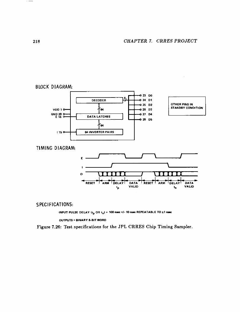
218 CHAPTER 7. CRRES PROJECT
BLOCK
TIMING
DIAGRAM:
IVDD 1 0---,
GND 29 o---- uE16_
115_ '_
DIAGRAM:
DECODER
DATA LATCHES
64 INVERTER PAIRS
F ,--0 23 DO16j 3 24 D1
J/ _.---,O25 D2
----O 26 D3
i ._O27 D428 D5
OTHER PINS IN
STANDBY CONDITION
E
I
D
,11RESET
__1 x I
/ %
xxxxxX
--I_'ARM_ IDELAY[-- DATA =1RESETrI-"ARMVlDELA_f I DATA
tp VALID tn VALID
SPECIFICATIONS:
INPUT PULSE DELAY (tp OR t n) = 100 nN¢ +/- 10 n=e¢ REPEATABLE TO+I nm¢
OUTPUTS = BINARY 8-BIT WORD
Figure 7.26: Test specifications for the JPL CRRES Chip Timing Sampler.

7.10. CRRES CHIP TEST CONFIGURATION PIN OUTS 219
4. CRRES Chip Pin Configuration for MOSFET Matrix Measurement. See
also Figures 7.1, 7.4, and 7.27.
PIN FUNCTION PIN STATE PIN FUNCTION PIN STATE
1 VDD VDD 33 SRAM DQ12 GND
2 XT VPS VDD 34 SRAM DQll GND
3 SPARE GND 35 SRAM DQ10 GND
4 XT VG VS 36 SRAM DQ9 GND
5 INVOUT NC 37 SRAMDQ8 GND
6 INV SUB VDD 38 SRAM DQ7 GND
7 INV VDD VDD 39 SRAM DQ6 GND
8 INV p-GATE GND 40 SRAM DQ5 GND
9 INVVSS GND 41 SRAM DQ4 GND10 INV WELL GND 42 SRAM DQ3 GND
11 XT WELL VS 43 SRAM DQ2 GND
12 INVn-GATE GND 44 SRAM DQ1 GND
13 SPARE GND 45 SRAM DQ0 GND14 SPARE GND 46 SRAM S GND
15 TS I GND 47 SRAM W GND16 TS E GND 48 SRAM E GND
17 SPARE GND 49 SRAM EP GND
18 SPARE GND 50 SRAM A5 GND
19 SPARE GND 51 SRAM A4 GND
20 SPARE GND 52 SRAMA3 GND21 SPARE GND 53 SRAM A2 GND
22 SPARE GND 54 SRAMA1 GND
23 TS DO NC 55 SRAM A0 GND
24 TS D1 NC 56 XT EN VDD
25 TS D2 NC 57 SPARE GND
26 TS D3 NC 58 XT R1 (0,I)
27 TS D4 NC 59 XT R0 (0,1)
28 TS D5 NC 60 XT CO (0,1)
29 GND GND 61 XTC1 (0,1)
30 SRAM DQ15 GND 62 XTC2 (0,1)31 SRAM DQ14 GND 63 XT ID VS,IM
32 SRAM DQ13 GND 64 XT VD DVMNC = NO CONNECTION
TS = TIMING SAMPLER
XT -- TRANSISTOR MATRIX
SRAM = STATIC RANDOM ACCESS MEMORY
INV = INVERTER
VS = VOLTAGE SOURCE; IM = CURRENT MEASURE
n-CH XT: COL 0, 2, 4, AND 6; p-CH XT: COL 1, 3, 5, AND 7
XT DIM: Col 1 & 2 W/L = 6/zm/3 #m; Col 3 & 4 W/L =- 9/zm/3 _m,
Col 5 & 6 W/L -- 6_m/3_m; Col 7 & 8 W/L -- 9/zm/3/_mLARGE FIELD OXIDE XT: ROW 0, COL 4 AND 6; BLANK: ROW 0, COL 5

220 CHAPTER 7. CRRES PROJECT
BLOCK D IAGRAM:
VDD 1
GND 29 O---
MEP SPECIFICATION:
lOS MEASURE
VDS MEASURE
VDS SUPPLY
VGS SUPPLY
TRANSISTOR I
MATRIX
I
60 61 62
CO C1 C2
1_ _±t0_TOlmA±0.5_RCENT
0TOSV±tmV
0TO5V±lmV
0TO5V±lmV
lOS - 0.05,0.2,0.6, 1, 1.5,2,2.5,3,3.5,4,4.5,5V
VGS - 0.05, 0.5, 1, 1.5, 2, 2.5, 3, 3.5, 4, 4.5, 5 V
VBS - 0
12 VOLTAGES
11 VOLTAGES
'--'O 11 WELL
•""04 VG
,m..O 2 VPS
•"-064 VD
_63 ID
56 ENABLE
TOTAL - 132 DATAPOINTS
OTHER PINS IN
STANDBY CONDITION
PREFERRED MEASUREMENT SPECIFICATION:
VOS - 0.05,0.2.0,6,1, 1.5,2,3.5,5V
VGS - 0.1, 0.2, 0.3, 0.4, 0.5, 0.8, 0.7,0.8, 0.g 1.0, 1.1, 1.5, 2. 3, 4, 5 V
VBS - 0
/8 VOLTAGES _. TOTAL - t28 DATA POINTS
16 VOLTAGES !
Figure 7.27: Test specifications for the JPL CRRES Chip MOSFET Matrix.

7.10.
o
CRRES CHIP TEST CONFIGURATION PIN OUTS 221
CRRES Chip Leakage Measurement Pin Configuration. Early CRRES
Runs Only: Foundry Run 1 (VTI1). This pin-out list is different in that
the Ring Oscillator had not yet been removed from the timing sampler
circuit
PIN FUNCTION PIN STATE PIN FUNCTION PIN STATE
1 VDD VDD 33 SRAM DQ12 GND
2 XTVPS VDD 34 SRAM DQll GND3 SRAM A7 GND 35 SRAM DQ10 GND
4 XT VG GND 36 SRAM DQ9 GND
5 INV OUT NC 37 SRAM DQ8 GND
6 INVSUB VDD 38 SRAM DQ7 GND
7 INV VDD VDD 39 SRAM DQ6 GND
8 INV p-GATE GND 40 SRAM DQ5 GND9 INV VSS GND 41 SRAM DQ4 GND
10 INV WELL GND 42 SRAM DQ3 GND
11 XT WELL GND 43 SRAM DQ2 GND
12 INV n-GATE GND 44 SRAM DQ1 GND
13 SPARE GND 45 SRAM DQ0 GND14 SPARE GND 46 SRAM S GND
15 TS I GND 47 SRAM W GND
16 TS E GND 48 SRAM E GND
17 RO ENABLE GND 49 SRAM EP GND
18 RO OUTPUT NC 50 SRAM A5 GND19 SPARE GND 51 SRAM A4 GND
20 SPARE GND 52 SRAM A3 GND
21 SPARE GND 53 SRAM A2 GND
22 SPARE GND 54 SRAM A1 GND
23 TS DO NC 5S SRAM A0 GND
24 TS D1 NC 56 XT EN GND
25 TS D2 NC 57 SRAM A6 GND
26 TS D3 NC 58 XT R1 GND
27 TS D4 NC 59 XT R0 GND
28 TS D5 NC 60 XT CO GND29 GND GND 61 XTC1 GND
30 SRAM DQ15 GND 62 XT G2 GND
31 SRAM DQ14 GND 63 XT ID NC
32 SRAM DQ13 GND 64 XT VD NC
NC = NO CONNECTION
TS = TIMING SAMPLER
XT = TRANSISTOR MATRIX
INV -- INVERTER
SRAM = STATIC RANDOM ACCESS MEMORY


Bibliography
[1] M. G. Buehler, T. W. Griswold, C. A. Pifia, and C. Timoc, "Test Chips for
Custom ICs: Six Kinds of Test Structures," Circuits Manufacturing, Vol.
22, pp. 36-42, June 1982.
[2] M. G. Buehler, B. R. Blaes, G. A. Jennings, B. T. Moore, R. H. Nixon,
C. A. Pifia, H. R. Sayah, M. W. Sievers, and N. F. Stahlberg, "Product
Assurance Technology for Custom LSI/VLSI Electronics Report for Period
October 1982 - September 1984," JPL Publication 85-76.
[3] M. G. Buehler, B. R. Blaes, C. A. Pifia, T. W. Griswold, "Pinhole Array
Capacitor for Oxide Integrity Analysis," Solid State Technology, Vol. 26,
pp. 131-137, November 1983.
[4] E. Kooi, J. G. van Lierop, J. A. Appels, "Formation of Silicon Nitride at
an Si-SiO2 Interface during Local Oxidation of Silicon and during Heat-
Treatment of Oxidized Silicon in NHz Gas," J. Electrochem. Soc., Vol. 123,
pp. 1117-1120, 1976.
[5] O. Nakajima, N. Shiono, S. Musamoto, and C. Hushimoto, "Defects in a
Gate Oxide Grown after the LOCOS Process," Jpn. J. Appl. Phys., Vol.
18, pp. 943-951, 1979.
[6] C. A. Goodwin and J. W. Brossman, "MOS Gate Oxide Defects Relatedto Treatment of Nitride Coated Wafers Prior Local Oxidation," J. Elec-
trochem. Soc., Vol. 129, pp. 1066-1070, 1982.
[7] U. Leineweg and D. Hannaman, "Yield Analysis of Interfacial Contact Re-
sistance Measured on Cross-Contact-Chains," IEEE VLS[ Workshop on
Test Structures, Long Beach, California, February 1986.
[8] J. Shen, W. Maly, and F. Ferguson, Carnegie-Mellon University, "Induc-
;rive Fault Analysis of MOS Integrated Circuits," IEEE Design and Test of
Computers, Vol. 2, pp 13-26, December 1985.
PRECEDING PAGE BLANK NOT FILMED
223
z-, ....

224
[91
[lO]
[11]
[12]
[13]
[14]
[15]
[16]
[171
[18]
[19]
BIBLIOGRAPHY
M. Buehler and H. Sayah, "Addressable Inverter Matrix for Process and
Device Characterization," Solid State Technology, Vol. 28, pp 185-191, May
1985.
Fail-Safe Technology, "Report on Failure Characteristics of the NMOS and
PMOS SMARTPAC," 18 July 1986.
H. Iwai and S. Kohyama, "On-Chip Capacitance Measurement Circuits in
VLSI Structures," IEEE Tran. Elec. Dev., Vol. ED-29, No. 10, pp. 1622-
1626, October 1982.
J. Paulos and D. Antoniadis, "Measurement of Minimum-Geometry MOS
Transistor Capacitances," IEEE Tran. Elec. Dev., Vol. ED-32, No. 2, pp.
357-363, February, 1985.
H. Iwai, J. Oristian, J. Walker, and R. Dutton, "A Scalable Technique for
the Measurement of Intrinsic MOS Capacitance with Atto-Farad Resolu-
tion," IEEE Tran. Elec. Dev., Vol. ED-32, No. 2, pp. 344-356, February,
1985.
M. Furukawa, H. Hatano, and K. Hanihara, "Precision Measurement Tech-
nique of Integrated MOS Capacitor Mismatching Using a Simple On-Chip
Circuit," IEEE Tran. Elee. Dev., Vol. ED-33, No. 7, pp. 938-944, July, 1986.
T. Chan, A. Wu, P. Ko, and C. Hu, "A Capacitance Method to Determine
the Gate-to-Drain/Source Overlap Length of MOSFET's," IEEE Elec. Dev.
Lett., Vol. EDL-8, No. 6, pp. 269-271, June, 1987.
P. Richman, MOS Field-Effect Transistors and Integrated Circuits, John
Wiley & Sons, New York, 1973.
N. Sasaki, "Higher Harmonic Generation in CMOS/SOS Ring Oscillators,"
IEEE Trans. Elec. Dev., Vol. ED-29, pp. 280-283, 1982.
T. W. Houston, "Comments on 'Higher Harmonic Generation in CMOS/
SOS Ring Oscillators,'" IEEE Trans. Elec. Dev., Vol. ED-30, pp. 958-959,
1983.
I. Ohkura, K. Okazaki, and Y. Horiba, "A New Exact Delay Logic Simu-
lation for ED MOS LSI," Proceedings IEEE Int. Conf. Cir. Comp., p. 953,
1980.
BIBLIOGRAPHY 225
[20] E. S. Anolock and L. Y. Chen, "Application of Step Stress to Time Depen-
dent Breakdown," Proc. 19th Rel. Phys. Syrup., _). 23, 1981.
[21] E. S. Anolock and L. Y. Chen, "Screening of Time Dependent Dielectric
Breakdown," Proc. 20th Rel. Phys. Syrup., p. 238, 1982.
[22] A. Berman, "Time-Zero Dielectric Reliability Test by a Ramp Method,"
Proc. 19th Rcl. Phys. Syrup., p. 204, 1981.
[23] P. S. Winokur, J. R. Schwank, P. J. McWorter, P. V. Dressendorfer, and
D. C. Turpin, "Correlating the Radiation Response of MOS Capacitors and
Transistors," IEEE Trans. on Nucl. Sci., Vol. NS-31, pp. 1453-1460, 1984.
[24] W. Fichtner and H. W. Potzl, "MOS Modeling by Analytical Approxima-
tions: Subthreshold Current and Threshold Voltage," Int. J. Elec., Vol. 46,
pp. 33 - 55, 1979.
[25] S. M. Sze, Physics of Semiconductor Devices, John Wiley and Sons, New
York, 1969.
[26] R. M. Swanson and J. D. Meindl, "Ion-Implanted CMOS transistors in
Low-Voltage Circuits," IEEE J. Solid-State Circ., SC-7, p. 145, 1972.
[27] A. Vladimirescu and S. Liu, "The Simulation of MOS Integrated Circuits
Using SPICE2," Memorandum No. UCB/ERL M80/7, February 1980.
[28] P. Antognetti, D. D. Caviglia, and E. Profumo, "CAD Model for Threshold
and Subthreshold Conduction in MOSFET's," IEEE J. Solid-State Circ.,
Vol. SC-17, pp. 454 - 458, 1982.
[29] A. H.-C. Fung, "A Subthreshold Conduction Model for BSIM," Memoran-
dum No. UCB/ERL M85/22, March 1985.
[3o] M. G. Buehler and Y.-S. Lin, "Comparison of Results From Simple Expres-
sions for MOSFET Parameter Extraction," Proc. IEEE Conf. Microelec-
tronic Test Structures, Vol. 1, pp. 90-96, 1988.
[31] R. L. Mattis, "A FORTRAN Program for Analysis of Data from Microelec-
tronic Text Structures," National Bureau of Standards Special Publication
400-75, July 1983.
[32] H. Akima, Collected Algorithms from ACM, Algorithm 526, revised June 61977: ACM 1978.

226 BIBLIOGRAPHY
[33] ACM Transactions on Mathematical Software, Vol. 4, No. 2, pp. 160-164,
June 1978.
[34] D. K. Nichols, W. E. Price, and C. Malone, "A Guideline for Heavy IonRadiation Testing for Single Event Upset," JPL Publication 84-22, 1984.
[35] M. G. Buehler, B. T. Moore, and R. H. Nixon. "Parameter Extraction from
Spacebourne MOSFETs," IEEE Trans. Nucl. Sci., NS-32, pp. 4237-4243,
1985.

1. Report No..TPT, pz_hl "ir_t-lnn _g-1
4. Title and Subtitle
2. Government Accession No.
Product Assurance Technology for Procuring Reliable
Radiatlon-Hard, Custom LSI/VLSI Electronics
7. Author_)M_G. Bu_hleT; R.A. Allen; B.R. Blaes;K.A.Hic_
G.A.Jennings; _f-S._in; C.A.Pina; H.R.Sayah; N. Zamani
TECHNICAL REPORT STANDARD TITLE PAGEi
3. Recipient's Catalog No.
5. Report Date
January 1989
6. Performing Organization Code
:s_. Performing Organization Report No.
9. Performing Organization Name and Address
JET PROPULSION LABORATORY
California Institute of Technology
4800 Oak Grove Drive
Pasadena, California 91109
12. Spons_ing Agency Name and Address
NATIONAL AERONAUTICS AND SPACE ADMINISTRATION
Washington, D.C. 20546
10. Work Unit No.
11. Contract or Grant No.NAS7-918
13. Type of Report and Period CoveredJPL Publication
Report for Period:
October 1984 - September 1986
14. Sponsoring Agency CodeREI91 BW-323-51-20-06-00
15. Supplementary Notes
16. A_tractIn this effort, advanced measurement methods that use microelectronic test chips are
described. These chips are intended to be used in acquiring the data needed to
qualify Application Specific Integrated Circuits (ASICs) for space use. This work
represents the collaborative effort of integrated-clrcuit (IC) parts specislists,
device physicists, test-chlp engineers, and fault-tolerant-circuit designers. Theiz
efforts were focused on developing the technology for obtaining custom ICs from
CMOS/bulk silicon foundries. In pursuit of this goal, a series of test chips has
been developed: a Parametric Test Strip, a Fault Chip, a set of RellabilJty Chips,
and the CRRES (Combined Release and Radiation Effects Satellite) Chip, a test
curcuit for monitoring space zadiation effects.
The technical accomplishments of the effort include: (I) Development of a Fault Chip
thst contains a set of test structures used to evaluate the density of various
process-induced defects; (2) Development of new test structures and testing
techniques for measuring gate-oxide capacitance, gate-overlap capacitance, and
propagation delay; (3) Development of a set of Reliability Chips that are used toevaluate failure mechanisms in CMOS/Bulk: interconnect and contact electromigration
and time-dependent dielectric breakdown; (4) Development of MOSFET parameter
extraction procedures for evaluating subthreshold characteristics; (5) Evaluation of
Test Chips and Test Strips on the second CRRES wafer run; (6) Two dedicated
fabrication runs for the CRRES Chip flight parts; and (7) Publication of two papers:
one on the Split-Cross Bridge Resistor and another on Asymmetrical SRAM Cells for
Single-Event Upset Analysis. ,.
17. Key Wor_ _elec_d by Aurora)) 18. Olstribut_n Statement
Microelectronic test chips; Custom
LSI/VLSI circuits; Product Assurance Unclassified - Unlimited
Methodology.
19. Security Clmslf. _f this repo_)
Unclassified
20. Security Clmsif. _f this page)
Unclassified
21. No. of Pages 22. Price
239
JPL O184 R 9183


,,t