Embed Size (px)
Citation preview

EE 200 Midterm Exam 20 March 2014
Last Name (Print):
First Name (Print):
ID number (Last 4 digits):
Section:
DO NOT TURN THIS PAGE UNTIL YOU ARE TOLD TO DO SO
Problem Weight Score
1 25
2 25
3 25
4 25
Total 100
INSTRUCTIONS
1. You have 2 hours to complete this exam.
2. This is a closed book exam. You may use one 8.5”× 11” note sheet.
3. Calculators are allowed.
4. Solve each part of the problem in the space following the question. If you need more space, continue your solutionon the reverse side labeling the page with the question number; for example, Problem 1.2 Continued. NO
credit will be given to solutions that do not meet this requirement.
5. DO NOT REMOVE ANY PAGES FROM THIS EXAM. Loose papers will not be accepted and agrade of ZERO will be assigned.
6. The quality of your analysis and evaluation is as important as your answers. Your reasoning must be preciseand clear; your complete English sentences should convey what you are doing. To receive credit, you must
show your work.
7. Any student caught cheating on an exam will receive a grade of zero for the exam. Additional sanctions,including assigning an XF grade, will be pursued following university guidelines.
1

Problem 1: (25 Points)
1. (11 points) Figure 1 shows the circuit diagram of a Moore finite state machine with input x and output y.
Figure 1: Discrete logic realization of a Moore finite state machine with input x and output y.
(a) (3 points) Determine expressions for DA, DB, and y in terms of x, QA, and QB.
(b) (8 points) Complete the state table in Table 1.
Present State Next State OutputQA QB x x y0 0
0 11 0
1 1
Table 1: State table for the Moore finite state machine in Figure 1.
2

2. (10 points) Table 2 shows the state table for another finite state machine, with inputs x and y, and output z.The notation xy indicates that the input x is in a logic low-state while the input y is in a logic high-state.For a given present state, input combinations that are not possible are indicated by X. Using the four-variableKarnaugh map in Figure 2, determine the excitation equation for the input DB to the D-type flip-flop whoseoutput is QB. To receive credit, mark all the minterms with either a 1, 0 or X (Don’t Care) in the Karnaughmap.
Present State Next State OutputSymbol QA QB xy xy xy xy z
S0 0 0 S0 X S0 S0 0S1 0 1 S0 S0 S1 S2 1S2 1 1 S2 S1 X X 1
Table 2: State table for a Moore finite state machine.
Figure 2: Four-variable Karnaugh map
3

3. (4 points) Realize the logic expressionw = xy + zx
using two-input NAND gates. Show all calculations needed to place the expression for w in a form suitable forimplementing with NAND gates, and neatly sketch the resulting discrete-logic circuit.
4

Problem 2: (25 Points)
1. (12 points) The circuit in Figure 3(A), with input vi(t) and output vo(t), uses a CMOS exclusive-or gate witha low-state output voltage VL = VSS = 0 V and a high-state output voltage VH = VDD. The circuit is drivenby the pulse in Figure 3(B). Immediately prior to the input pulse that is applied at time 0, there is no energystored in the capacitor. Neatly sketch the resulting waveforms vC(t) and vo(t) in Figure 4 on page 6. To receivefull credit:
• Carefully label the maximum amplitude of the waveforms vC(t) and vo(t).
• Determine the width of any pulse appearing in the output vo(t) in terms of the parameters R and C.
• Show the calculations used to derive the pulse width in terms of the parameters R and C.
• Indicate the pulse width in Figure 4.
Figure 3: (A) CMOS circuit with input vi(t) and output vo(t) and (B) the input waveform vi(t).
5

Figure 4: Input and output waveforms for the circuit in Figure 3.
6

2. (13 points) The passive network in Figure 5 implements a filter network with input voltage f(t) and outputvoltage y(t).
Figure 5: Passive filter network.
(a) (7 points) The frequency response function of the network in Figure 5 has the form
H(ω) =Y
F= K
1
ω/ωc + 1,
where Y and F are the phasor representations of the output and input respectively. Express the parametersK and ωc in terms of R1, R2, and C.
7

8

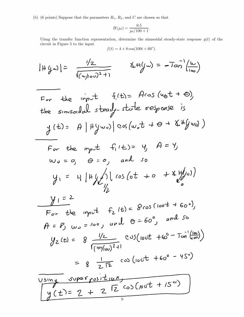
(b) (6 points) Suppose that the parameters R1, R2, and C are chosen so that
H(ω) =0.5
ω/100 + 1.
Uisng the transfer function representation, determine the sinusoidal steady-state response y(t) of thecircuit in Figure 5 to the input
f(t) = 4 + 8 cos(100t + 60◦).
9

Problem 3: (25 Points)
1. (7 points) For the LabVIEW block diagram appearing in Figure 6:
• (2 point) Specify if the output indicator displays a scalar, a 1D array, or a 2D array, as well as its datatype, for example, a 32-bit signed integer.
• (5 points) Determine the value(s) displayed by the indicator. If the output is a 1D array, you must expressyour answer as a row or column vector with the correct dimension. If the output is a 2D array, you mustshow the correct number of rows and columns. Show work for partial credit.
Figure 6: Block diagram for Problem 3 Part 1.
10

2. (5 points) Determine the value displayed by the indicator in the LabVIEW block diagram appearing in Figure7. Show work for partial credit.
Figure 7: Block diagram for Problem 3 Part 2.
11

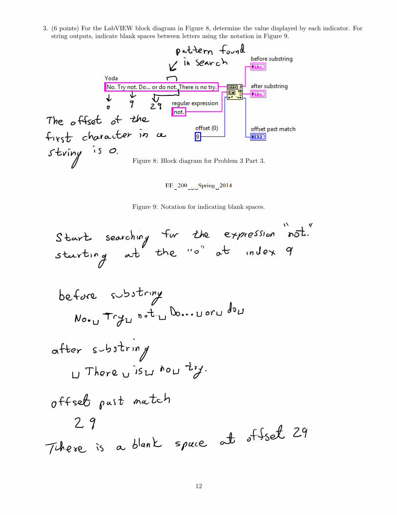
3. (6 points) For the LabVIEW block diagram in Figure 8, determine the value displayed by each indicator. Forstring outputs, indicate blank spaces between letters using the notation in Figure 9.
Figure 8: Block diagram for Problem 3 Part 3.
Figure 9: Notation for indicating blank spaces.
12

4. (7 points) For the LabVIEW block diagram appearing in Figure 10:
• (2 point) Specify if the output indicator displays a scalar, a 1D array, or a 2D array, as well as its datatype, for example, a 1D array of ten 32-bit signed integers.
• (5 point) Determine the value(s) displayed by the indicator. If the output is a 1D array, you must indicatethe value of every element of the array.
Figure 10: Block diagram for Problem 3 Part 4.
13

Problem 4: (25 Points)
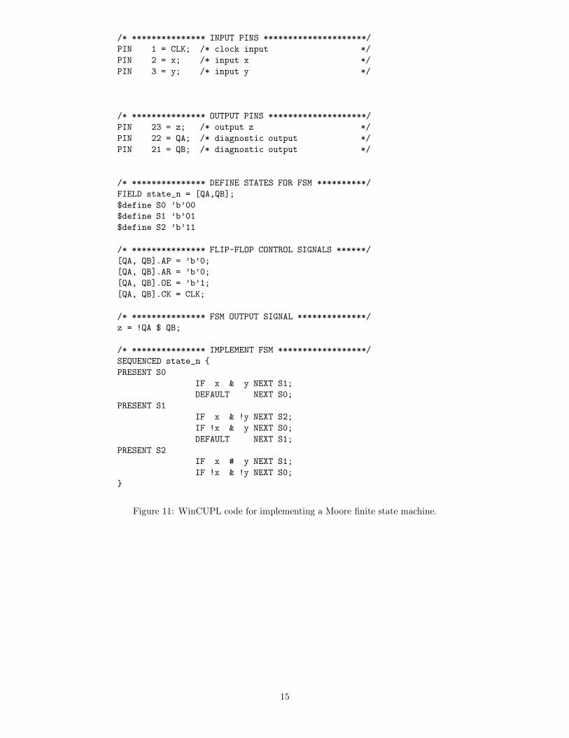
1. (10 points) Figure 11 on page 15 shows the HDL code for realizing a Moore finite state machine using theATMEL 750CL programmable logic device. The finite state machine has three states S0, S1, and S2, twoinputs x and y, and one output z.
(a) (7 points) Draw the state state diagram representation of the Moore finite state machine realized by theHDL code in Figure 11 on 15.
(b) (3 points) Modify the HDL code to include an asynchronous reset that drives the finite state machine tostate S0 when the logic level on pin 4 goes from a logic-high state to a logic low-state. In the space below,write the required modified and/or additional lines of code and include appropriate comment statements.
14

/* *************** INPUT PINS *********************/
PIN 1 = CLK; /* clock input */
PIN 2 = x; /* input x */
PIN 3 = y; /* input y */
/* *************** OUTPUT PINS ********************/
PIN 23 = z; /* output z */
PIN 22 = QA; /* diagnostic output */
PIN 21 = QB; /* diagnostic output */
/* *************** DEFINE STATES FOR FSM **********/
FIELD state_n = [QA,QB];
$define S0 ’b’00
$define S1 ’b’01
$define S2 ’b’11
/* *************** FLIP-FLOP CONTROL SIGNALS ******/
[QA, QB].AP = ’b’0;
[QA, QB].AR = ’b’0;
[QA, QB].OE = ’b’1;
[QA, QB].CK = CLK;
/* *************** FSM OUTPUT SIGNAL **************/
z = !QA $ QB;
/* *************** IMPLEMENT FSM ******************/
SEQUENCED state_n {
PRESENT S0
IF x & y NEXT S1;
DEFAULT NEXT S0;
PRESENT S1
IF x & !y NEXT S2;
IF !x & y NEXT S0;
DEFAULT NEXT S1;
PRESENT S2
IF x # y NEXT S1;
IF !x & !y NEXT S0;
}
Figure 11: WinCUPL code for implementing a Moore finite state machine.
15

2. (8 points) Figure 12 shows the SPICE model for an amplifier realized as a Multisim component. Draw aschematic representation of the component. To receive credit:
• Specify the numeric value of each component.
• Label each node using the designations (1), (2), (3), and (4).
• For dependent sources, indicate the controlling variable and its polarity, or reference direction, in yourschematic.
.SUBCKT Amp 1 4
RR1 1 2 50
RR2 2 0 10MEG
RR3 2 4 1K
RR4 3 4 100
CC1 2 4 0.01U
Eg 3 0 0 2 .1MEG
.ENDS Amp
Figure 12: SPICE model for a Multisim component that realizes an amplifier.
16

3. (7 points) Figures 13 and Figure 14 on page 18 shows an amplifier and its printed circuit board layout,respectively. The printed circuit board layout is consistent with the schematic; there are no wiring errors.What recommendations would you make regarding the layout? Assign each of your suggestions a number, andin Figure 14, circle the affected region and label the circle with the corresponding suggestion number.
17

Figure 13: Amplifier circuit diagram.
Figure 14: Realization of the amplifier using the top layer of a printed circuit board.
18

EE 200 Midterm Exam 20 March 2014
Last Name (Print):
First Name (Print):
ID number (Last 4 digits):
Section:
DO NOT TURN THIS PAGE UNTIL YOU ARE TOLD TO DO SO
Problem Weight Score
1 25
2 25
3 25
4 25
Total 100
INSTRUCTIONS
1. You have 2 hours to complete this exam.
2. This is a closed book exam. You may use one 8.5”× 11” note sheet.
3. Calculators are allowed.
4. Solve each part of the problem in the space following the question. If you need more space, continue your solutionon the reverse side labeling the page with the question number; for example, Problem 1.2 Continued. NO
credit will be given to solutions that do not meet this requirement.
5. DO NOT REMOVE ANY PAGES FROM THIS EXAM. Loose papers will not be accepted and agrade of ZERO will be assigned.
6. The quality of your analysis and evaluation is as important as your answers. Your reasoning must be preciseand clear; your complete English sentences should convey what you are doing. To receive credit, you must
show your work.
7. Any student caught cheating on an exam will receive a grade of zero for the exam. Additional sanctions,including assigning an XF grade, will be pursued following university guidelines.
1

Problem 1: (25 Points)
1. (11 points) Figure 1 shows the circuit diagram of a Moore finite state machine with input x and output y.
Figure 1: Discrete logic realization of a Moore finite state machine with input x and output y.
(a) (3 points) Determine expressions for DA, DB, and y in terms of x, QA, and QB.
(b) (8 points) Complete the state table in Table 1.
Present State Next State OutputQA QB x x y0 0
0 11 0
1 1
Table 1: State table for the Moore finite state machine in Figure 1.
2

2. (10 points) Table 2 shows the state table for another finite state machine, with inputs x and y, and output z.The notation xy indicates that the input x is in a logic low-state while the input y is in a logic high-state.For a given present state, input combinations that are not possible are indicated by X. Using the four-variableKarnaugh map in Figure 2, determine the excitation equation for the input DB to the D-type flip-flop whoseoutput is QB. To receive credit, mark all the minterms with either a 1, 0 or X (Don’t Care) in the Karnaughmap.
Present State Next State OutputSymbol QA QB xy xy xy xy z
S0 0 0 S0 X S0 S0 0S1 0 1 S0 S0 S1 S2 1S2 1 1 S2 S1 X X 1
Table 2: State table for a Moore finite state machine.
Figure 2: Four-variable Karnaugh map
3

3. (4 points) Realize the logic expressionw = xy + zx
using two-input NAND gates. Show all calculations needed to place the expression for w in a form suitable forimplementing with NAND gates, and neatly sketch the resulting discrete-logic circuit.
4

Problem 2: (25 Points)
1. (12 points) The circuit in Figure 3(A), with input vi(t) and output vo(t), uses a CMOS exclusive-or gate witha low-state output voltage VL = VSS = 0 V and a high-state output voltage VH = VDD. The circuit is drivenby the pulse in Figure 3(B). Immediately prior to the input pulse that is applied at time 0, there is no energystored in the capacitor. Neatly sketch the resulting waveforms vC(t) and vo(t) in Figure 4 on page 6. To receivefull credit:
• Carefully label the maximum amplitude of the waveforms vC(t) and vo(t).
• Determine the width of any pulse appearing in the output vo(t) in terms of the parameters R and C.
• Show the calculations used to derive the pulse width in terms of the parameters R and C.
• Indicate the pulse width in Figure 4.
Figure 3: (A) CMOS circuit with input vi(t) and output vo(t) and (B) the input waveform vi(t).
5

Figure 4: Input and output waveforms for the circuit in Figure 3.
6

2. (13 points) The passive network in Figure 5 implements a filter network with input voltage f(t) and outputvoltage y(t).
Figure 5: Passive filter network.
(a) (7 points) The frequency response function of the network in Figure 5 has the form
H(ω) =Y
F= K
1
ω/ωc + 1,
where Y and F are the phasor representations of the output and input respectively. Express the parametersK and ωc in terms of R1, R2, and C.
7

8
(b) (6 points) Suppose that the parameters R1, R2, and C are chosen so that
H(ω) =0.5
ω/100 + 1.
Uisng the transfer function representation, determine the sinusoidal steady-state response y(t) of thecircuit in Figure 5 to the input
f(t) = 4 + 8 cos(100t + 60◦).
9

Problem 3: (25 Points)
1. (7 points) For the LabVIEW block diagram appearing in Figure 6:
• (2 point) Specify if the output indicator displays a scalar, a 1D array, or a 2D array, as well as its datatype, for example, a 32-bit signed integer.
• (5 points) Determine the value(s) displayed by the indicator. If the output is a 1D array, you must expressyour answer as a row or column vector with the correct dimension. If the output is a 2D array, you mustshow the correct number of rows and columns. Show work for partial credit.
Figure 6: Block diagram for Problem 3 Part 1.
10

2. (5 points) Determine the value displayed by the indicator in the LabVIEW block diagram appearing in Figure7. Show work for partial credit.
Figure 7: Block diagram for Problem 3 Part 2.
11
3. (6 points) For the LabVIEW block diagram in Figure 8, determine the value displayed by each indicator. Forstring outputs, indicate blank spaces between letters using the notation in Figure 9.
Figure 8: Block diagram for Problem 3 Part 3.
Figure 9: Notation for indicating blank spaces.
12

4. (7 points) For the LabVIEW block diagram appearing in Figure 10:
• (2 point) Specify if the output indicator displays a scalar, a 1D array, or a 2D array, as well as its datatype, for example, a 1D array of ten 32-bit signed integers.
• (5 point) Determine the value(s) displayed by the indicator. If the output is a 1D array, you must indicatethe value of every element of the array.
Figure 10: Block diagram for Problem 3 Part 4.
13

Problem 4: (25 Points)
1. (10 points) Figure 11 on page 15 shows the HDL code for realizing a Moore finite state machine using theATMEL 750CL programmable logic device. The finite state machine has three states S0, S1, and S2, twoinputs x and y, and one output z.
(a) (7 points) Draw the state state diagram representation of the Moore finite state machine realized by theHDL code in Figure 11 on 15.
(b) (3 points) Modify the HDL code to include an asynchronous reset that drives the finite state machine tostate S0 when the logic level on pin 4 goes from a logic-high state to a logic low-state. In the space below,write the required modified and/or additional lines of code and include appropriate comment statements.
14
/* *************** INPUT PINS *********************/
PIN 1 = CLK; /* clock input */
PIN 2 = x; /* input x */
PIN 3 = y; /* input y */
/* *************** OUTPUT PINS ********************/
PIN 23 = z; /* output z */
PIN 22 = QA; /* diagnostic output */
PIN 21 = QB; /* diagnostic output */
/* *************** DEFINE STATES FOR FSM **********/
FIELD state_n = [QA,QB];
$define S0 ’b’00
$define S1 ’b’01
$define S2 ’b’11
/* *************** FLIP-FLOP CONTROL SIGNALS ******/
[QA, QB].AP = ’b’0;
[QA, QB].AR = ’b’0;
[QA, QB].OE = ’b’1;
[QA, QB].CK = CLK;
/* *************** FSM OUTPUT SIGNAL **************/
z = !QA $ QB;
/* *************** IMPLEMENT FSM ******************/
SEQUENCED state_n {
PRESENT S0
IF x & y NEXT S1;
DEFAULT NEXT S0;
PRESENT S1
IF x & !y NEXT S2;
IF !x & y NEXT S0;
DEFAULT NEXT S1;
PRESENT S2
IF x # y NEXT S1;
IF !x & !y NEXT S0;
}
Figure 11: WinCUPL code for implementing a Moore finite state machine.
15

2. (8 points) Figure 12 shows the SPICE model for an amplifier realized as a Multisim component. Draw aschematic representation of the component. To receive credit:
• Specify the numeric value of each component.
• Label each node using the designations (1), (2), (3), and (4).
• For dependent sources, indicate the controlling variable and its polarity, or reference direction, in yourschematic.
.SUBCKT Amp 1 4
RR1 1 2 50
RR2 2 0 10MEG
RR3 2 4 1K
RR4 3 4 100
CC1 2 4 0.01U
Eg 3 0 0 2 .1MEG
.ENDS Amp
Figure 12: SPICE model for a Multisim component that realizes an amplifier.
16

3. (7 points) Figures 13 and Figure 14 on page 18 shows an amplifier and its printed circuit board layout,respectively. The printed circuit board layout is consistent with the schematic; there are no wiring errors.What recommendations would you make regarding the layout? Assign each of your suggestions a number, andin Figure 14, circle the affected region and label the circle with the corresponding suggestion number.
17
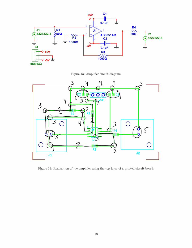
Figure 13: Amplifier circuit diagram.
Figure 14: Realization of the amplifier using the top layer of a printed circuit board.
18