Embed Size (px)
DESCRIPTION
Problem in book Fundamentals of Digital Logic with VHDL Design 3rd Ed
Citation preview
Aji Widhi Wibowo @2013 Jawaban sebisanya “Fundamentals of Digital Logic with VHDL Design 3rd Edition” -- S.Brown & Z.Vranesic
1 | P a g e
Problem 7.31
Modify the code in Figure 7.67 to use the control circuit in Figure
7.59. Synthesize the code for implementation in a chip and perform
a timing simulation.
Untuk mendapatkan hasil sirkuit seperti Figure 7.59 maka harus
dilakukan beberapa tahap.
Tahap pertama dilakukan untuk menghasilkan blok D flipflop yang
memiliki output Qbar. Karena dalam CAD, D flipflop yang dihasilkan
Aji Widhi Wibowo @2013 Jawaban sebisanya “Fundamentals of Digital Logic with VHDL Design 3rd Edition” -- S.Brown & Z.Vranesic
2 | P a g e
dengan VHDL tidak memiliki output Qbar maka untuk membuat
Qbar, D flipflop diberi sinyal internal untuk digunakan dalam blok
prosesnya. Barulah hasil sinyal digunakan sebagai output Qbar
dengan inverse.
-- D Flip Flop
library ieee;
use ieee.std_logic_1164.all;
entity d_ff is
port(D, Clock, Reset : in std_logic;
Q, Qbar : out
std_logic);
end entity d_ff;
architecture customsignal of d_ff is
signal state : std_logic;
begin
p0: process(Clock, Reset) is begin
if Reset='0' then
state <= '0';
else
if Clock'event and Clock='1' then
state <= D;
end if;
end if;
end process p0;
Q <= state;
Qbar <= not state;
end architecture customsignal;
dengan kode VHDL di atas maka akan menghasilkan Figure 1.
Figure 1: D flipflop
Kemudian D flipflop di atas digunakan sebagai blok D fliplop baru
(Figure 2) yang seakan sudah memiliki Qbar.
Figure 2: D flip flop dengan Qbar
D flipflop dengan Qbar dibutuhkan untuk membuat output untuk
R2out, R3in seperti yang dibutuhkan pada Figure 7.59.
Gambaran secara utuh control yang ada pada Figure 7.59 seperti
Figure 3.

Aji Widhi Wibowo @2013 Jawaban sebisanya “Fundamentals of Digital Logic with VHDL Design 3rd Edition” -- S.Brown & Z.Vranesic
3 | P a g e
Figure 3: modified control
Kode VHDL swapmux (Figure 7.67) dirubah untuk dapat melakukan
proses swap / tukar nilai.
Untuk bagian VHDL swapmux yang dirubah adalah sebagai berikut:
...
package components is
...
component shiftr --left to righ shift
register with async reset
generic(K: integer:=4);
port(Resetn, Clock, w : in
std_logic;
Q, Qbar, Qout: buffer
std_logic_vector(1 to K) );
end component;
...
end components;
...
architecture bhvr of swapmux is
signal Rin, Q, Qbar, Qout:
std_logic_vector(1 to 3);
...
begin
control: shiftr generic map(K => 3)
port map (Resetn, Clock, w, Q, Qbar,
Qout);
Rin(1) <= RinExt(1) or Qout(3);
Rin(2) <= RinExt(2) or Qout(2);
Rin(3) <= RinExt(3) or Qout(1);
muxes: with Qout select
BusWires <= Data when "000",
R2 when "100",
R1 when "010",
R3 when others;
...
end bhvr;
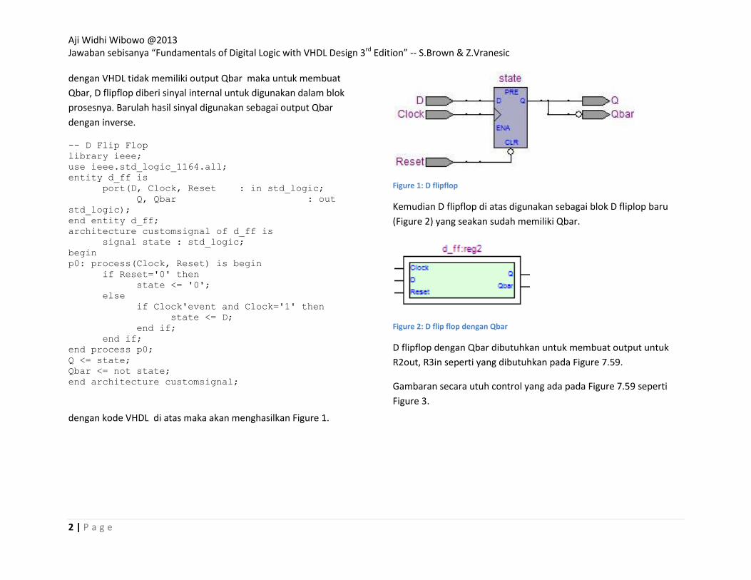
Hasil timing simulation dapat dilihat pada Figure 4
Aji Widhi Wibowo @2013 Jawaban sebisanya “Fundamentals of Digital Logic with VHDL Design 3rd Edition” -- S.Brown & Z.Vranesic
4 | P a g e
Figure 4: tukar nilai / swap register 1 dan 2
Figure 4 pada nilai waktu sekitar 580ns, w bernilai 1 yang
membangkitkan perintah untuk menukar nilai. Nilai register 1
ditukar dengan nilai register 2 menggunakan register 3 sebagai
register transitnya. Pertama nilai register 2 akan dikopi ke register 3,
kemudian nilai register 2 diganti dengan nilai register 1. Setelah
selesai barulah nilai register 1 digantikan dengan nilai dari register 3
yang sebelumnya merupakan nilai register 2.
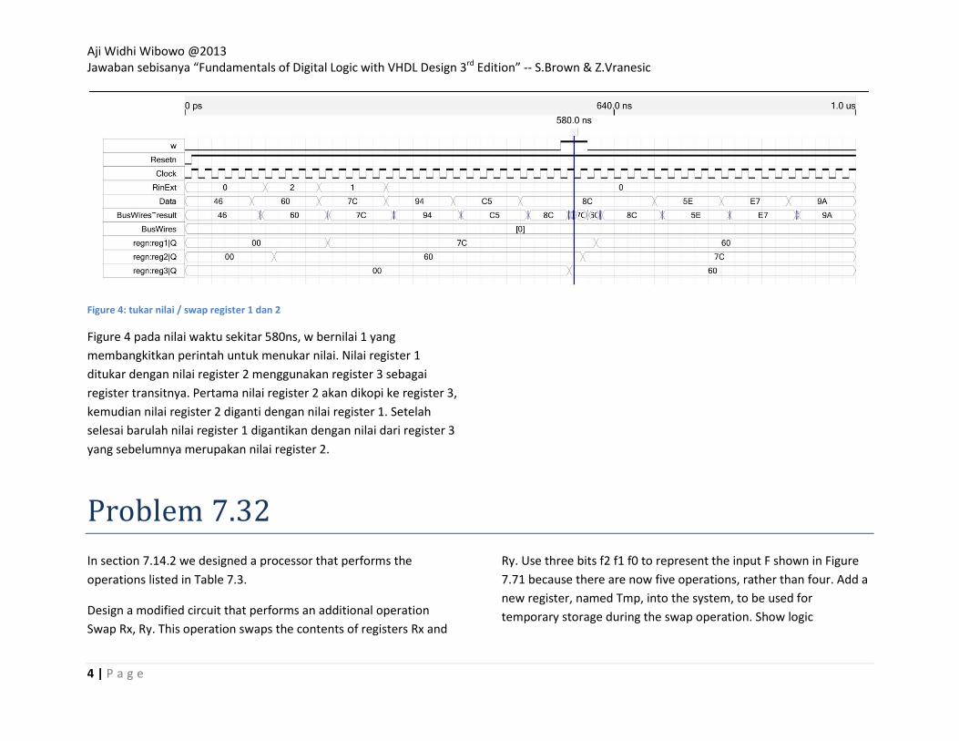
Problem 7.32
In section 7.14.2 we designed a processor that performs the
operations listed in Table 7.3.
Design a modified circuit that performs an additional operation
Swap Rx, Ry. This operation swaps the contents of registers Rx and
Ry. Use three bits f2 f1 f0 to represent the input F shown in Figure
7.71 because there are now five operations, rather than four. Add a
new register, named Tmp, into the system, to be used for
temporary storage during the swap operation. Show logic

Aji Widhi Wibowo @2013 Jawaban sebisanya “Fundamentals of Digital Logic with VHDL Design 3rd Edition” -- S.Brown & Z.Vranesic
5 | P a g e
expressions for the outputs of the control circuit, as was done in
section 7.14.2.
Hasil simulasi Timing operasi swap seperti gambar 2. Sinyal F
ditambahkan dari semula f1 dan f0 untuk menampung 4 instruksi,
menjadi f2, f1, f0 agar dapat menampung 5 intruksi. Sinyal “1xx”
akan akan melakukan swap nilai pada register alamat Rx dan Ry.
Rancangan langkah swap secara umum sebagai berikut:
Pada counter “01” nilai register dengan pointer Rx disimpan ke
register Tmp dan nilai register pointer Ry dipindah ke Rx.
Pada counter “10” nilai register Tmp akan dimasukkan ke nilai
register Rx melalui BusWires.
Figure 5: simulasi timing instruksi swap processor

Aji Widhi Wibowo @2013 Jawaban sebisanya “Fundamentals of Digital Logic with VHDL Design 3rd Edition” -- S.Brown & Z.Vranesic
6 | P a g e
Fungsi swap pada contoh simulasi di atas adalah “111”, tetapi
sebenarnya perintah swap bernilai “1xx” dengan ‘x’ bernilai
berapapun. Proses swap mulai berjalan ditandai dengan sinyal
w=1. Rx dan Ry merupakan petunjuk register mana yang akan di
swap, pada simulasi di atas register 2 dan 3 akan di-swap. Nilai
dari register ini masing-masing tersimpan pada regn:reg2|Q dan
regn:reg3|Q yang masing masing semula bernilai 204 dan 1.
Pada 240ns swap dilaksanakan ditandai dengan nilai TmpSave=1
sehingga Rx ( reg2|Q ) disimpan nilainya pada register Tmp saat
clock TmpSave bernilai 1 tersebut.
Nilai sebagai selector register mana yang akan dimasukkan ke
register Tmp adalah: R0 = “100”, R1 = “101”, R2 = “110”, R3 =
“111”.
Sedangkan untuk step yang dilakukan per counter:
T1 T2
TmpSave = 1, Rin = X, Rout = Y
Rin = Y, Rout = “1111”, Done = 1
Kode VHDL proc alternative (Figure 7.74) yang dirubah:
...
I <= FuncReg(1 TO 3) ;
functionreg: regn GENERIC MAP ( N => 7 )
PORT MAP ( Func, FRin, Clock, FuncReg ) ;
decX: dec2to4 PORT MAP ( FuncReg(4 to 5), High, X ) ;
decY: dec2to4 PORT MAP ( FuncReg(6 to 7), High, Y ) ;
controlsignal: PROCESS(T, I, X, Y) BEGIN
...
TmpSave <= '0';
case I(0) is
when '1' => --swap
case T is
when "00" =>
when "01" =>
TmpSave <= '1';
Rin <= X;
Rout <= Y;
when others =>
Rin <= Y;
Rout <= "1111";
Done <= '1';
end case;
when others =>
CASE T IS
WHEN "00" =>
WHEN "01" =>
...
END CASE;
...
end case;
END PROCESS;
WITH Sel SELECT
BusWires <= R0 WHEN "100000",
R1 WHEN "010000",
R2 WHEN "001000",
R3 WHEN "000100",
Tmp when "111100",
G WHEN "000010",
Data WHEN OTHERS;
with TmpSave & Rx select
Tmp <= R0 when "100",
R1 when "101",
R2 when "110",
R3 when "111",
unaffected when others;
...

Aji Widhi Wibowo @2013 Jawaban sebisanya “Fundamentals of Digital Logic with VHDL Design 3rd Edition” -- S.Brown & Z.Vranesic
7 | P a g e
Problem 7.33
A ring oscillator is a circuit that has an odd number, n, of inverters
connected in a ring like structure, as shown in Figure P7.5. The
output of each inverter is a periodic signal with a certain period.
(a) Assume that all the inverters are identical; hence they all have
the same delay, called tp. Let the output of one of the inverters be
named f . Give an equation that expresses the period of the signal f
in terms of n and tp.
Berdasarkan sumber slide 15/31
(http://www.uio.no/studier/emner/matnat/ifi/INF4420/v12/underv
isningsmateriale/INF4420_12_Ringoscillators_Print.pdf) frekuensi
dari ring oscillator adalah
f = 1/(2n∙tp)
Jadi periodenya adalah
T = 1/f = 2n∙tp
Problem 7.34
A circuit for a gated D latch is shown in Figure P7.7. Complete the timing diagram given in the figure P7.7

Aji Widhi Wibowo @2013 Jawaban sebisanya “Fundamentals of Digital Logic with VHDL Design 3rd Edition” -- S.Brown & Z.Vranesic
8 | P a g e
Figure 6: hasil simulasi D latch dengan 4 gerbang nand dan 1 inverter