Embed Size (px)
Citation preview

©2004 Robert S. Balog Jr., PE 1
Printed Circuit Boards Part I – Overview
Robert S. Balog Jr., PE

©2004 Robert S. Balog Jr., PE 2
Overview – Part I• Motivation• Cost issues• PCB Design Process• Post Design Process• PCB Manufacturing Overview

©2004 Robert S. Balog Jr., PE 3
PCB Advantages• Reliability of design
– Tight circuit design– No loose wires to pop-out
• Repeatability of experiments– Physically rugged– Archival design– No “black magic” to recreate original results
• Control of geometric considerations– Stray inductances and capacitances
• Cost of development– Time spend wire-wrapping and debugging vs. PCB design
• Marketable engineering skill

©2004 Robert S. Balog Jr., PE 4
PCB Disadvantages• Learning Curve
– Software– Layout skills– DFM – Design for Manufacturability
• Investment in time to create custom footprints.– Up-front investment in time – Mitigated by UIUC library of known good parts
• Fixed cost of PCB order

©2004 Robert S. Balog Jr., PE 5
PCB Development InvestmentUp-front vs. back-end costs
– PCB design: large initial investment– Vector board: trouble shooting / debugging commitment– Archival issues:– Cost recovery by communizing on parts in laboratory– Re-use known-good footprints

©2004 Robert S. Balog Jr., PE 6
PCB Vendor Cost Drivers• Material
– $0.167 per sq in. on prototype order– $0.153 per sq in on 50k production order
• Time– Engineer time – CAM review– Machine time– Delivery / shipping
• Pay for fast turn use UPS RED

©2004 Robert S. Balog Jr., PE 7
Delivery ScheduleHow fast do you need it? Ie a little bit of planning...• Prototype Service:
– Fast board turn options– Tooling costs included– Limitations on process capability (usually sufficient for our purposes)– 3 days 1 day: 96% premium (5pcs. 5” x 6”)
PROTOTYPE Price Matrix - unit price Qty 5-day 4-day 3-day 2-day
Best Value! 1-day same-day 5 N/A N/A $72.20 $87.20 $142.20 $182.20 10 N/A N/A $44.40 $51.90 $79.40 $99.40
• 3 for $33 ea. Special:– 5 day lead time– Limited process capability (1oz only)– Max. 85 sq. in. (8.5” x 10”)– 33 special 3 day proto service: 118% premium (5 pcs)

©2004 Robert S. Balog Jr., PE 8
Delivery ScheduleHow fast do you need it? Ie a little bit of planning...• Production Service:
– Fast board turn options– Tooling costs extra– Lowest cost in quantity– Designed for higher volume, longer delivery schedules– Full production capability– 2 weeks 3 days: 43% premium (50k pcs. 5” x 6”)
PRODUCTION Price Matrix - unit price
Qty 4-week 2-week 1-week
Best Value!
4-day 3-day 2-day 1-day same-day
5 $34.59 $48.43 $55.34 $63.99 $69.18 $89.93 $134.90 $169.491000 $4.74 $6.64 $7.58 $8.77 $9.48 $12.32 $18.49 $23.23
50000 $4.59 $6.43 $7.35 $8.50 $9.19 $11.94 $17.91 $22.51

©2004 Robert S. Balog Jr., PE 9
Design Process1. Electrical Circuit Design
Topologically correct, critical values (caps, inductors, power R)Breadboard testedDesign review with PI, Jonathan Kimball
2. DocumentationReview ECE Power Design Archives specification file:
SD00001-001 PCB File Management.doc3. Cadence Orcad Capture CIS v10.1 (PSD 15.1)
Topological schematicLogical flow not physical flowDRC
4. Cadence Orcad Layout Plus v10.1 (PSD 15.1)Signal / power flowComponent footprintsPadstacksDRC

©2004 Robert S. Balog Jr., PE 10
Post-Design Process1. Don’t rush. Up to 3pm counts as day #12. DRC (Design Rule Check)
SchematicLayout
3. FREE DFM at Advanced CircuitsOnly examples of errors, not each occurrenceFix errors and Re-run
4. OrderUpload DataCoordinate with Jonathan Kimball to place order
5. Watch e-mailWithin 1st day on-hold notice if problems

©2004 Robert S. Balog Jr., PE 11
Design Considerations
Cost Driver Design Stage Material Machine time Process Prototype Production Panel Utilization X X Layer Count X X X X Copper Thickness X X # hole sizes X X Minimum hole size X X X Internal corners X X Trace Spacing X X X

©2004 Robert S. Balog Jr., PE 12
Copper Weight1 oz of copper will cover 1 sq. ft. when rolled out to
a thickness of 0.0014” or 1.4 mil
Copper Weight/Thickness Table
Weight
1/2 oz. 1 oz. 2 oz.
Thickness
0.0007 0.0012” - 0.0014”
0.0028

©2004 Robert S. Balog Jr., PE 13
Printed Circuit Boards Part II – Manufacturing
Robert S. Balog Jr., PE

©2004 Robert S. Balog Jr., PE 14
Overview – Part II• Structure• Core Laminate• Drilling• Photo imaging process• Photo tools• Solder Mask• Finishes• Legend• Routing

©2004 Robert S. Balog Jr., PE 15
Printed Circuit BoardRigid Laminate material (FR4, typ.) consisting of a glass
epoxy substrate clad with copper on two sides for double side (0.062” typ.)
Typically in sheets at ½ oz. and 1 oz. Per square foot in weight (0.0007 and 0.0014 inches nominal thickness respectively).

©2004 Robert S. Balog Jr., PE 16
PrepregMultilayer “glue”Woven Fiberglass cloth pre-impregnated with
partially cured epoxy resinAlso known as B-stageThe Resin is activated and “melts” during the
lamination process from pressure and heat.It flows across oxide coating on the core to create
bond.

©2004 Robert S. Balog Jr., PE 17
Primary DrillingHoles are drilled through a stack of panels (usually 2
to 3 high)Drilled hole sizes are typically 5 mils larger than
finished plated through hole sizes

©2004 Robert S. Balog Jr., PE 18
Dry Film Photo ResistLight sensitive film is
applied, using heat and pressure, to the copper surfaces of the laminated panel.
Film also covers, or tents, all drilled holes

©2004 Robert S. Balog Jr., PE 19
Photo Tools (Artwork)The gerber data for the panel is used to plot film that
depicts the circuits and traces of the board. The photo tools or artwork includes solder mask and nomenclature or legend too.
File Names
*.TOP = Top Copper
*.BOT = Bottom Copper
*.SMT = Solder Mask Top
*.SMB = Solder Mast Bottom
*.SST = Silk Screen (legend) TOP

©2004 Robert S. Balog Jr., PE 20
ExposePanels are exposed to a high intensity light source
coming through the film. Clear areas allow light to pass through and polymerize (harden) the film resist thus creating a latent image of the circuit pattern – just like a photograph.
©2004 Robert S. Balog Jr., PE 21
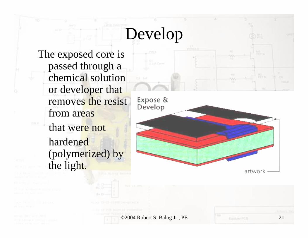
DevelopThe exposed core is
passed through a chemical solution or developer that removes the resist from areas that were not hardened (polymerized) by the light.

©2004 Robert S. Balog Jr., PE 22
EtchCopper is chemically
removed from the core in all areas not covered by film resist.
This creates a discrete copper pattern that matches the film pattern.
The core laminate surface now shows through in areas where copper was etched away.
©2004 Robert S. Balog Jr., PE 23
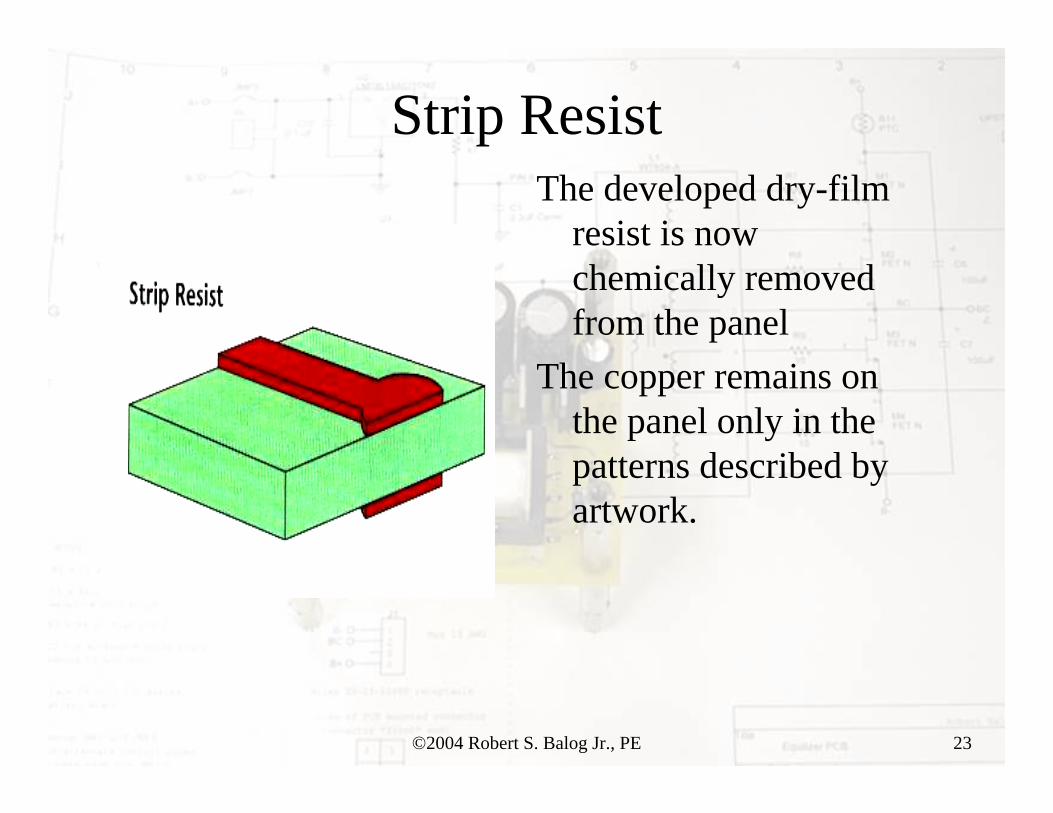
Strip ResistThe developed dry-film
resist is now chemically removed from the panel
The copper remains on the panel only in the patterns described by artwork.

©2004 Robert S. Balog Jr., PE 24
Copper Pattern PlateAlso called electroplating, additional copper is
electrically plated onto the exposed electrolesscopper surfaces.
The plated Copper thickness is approximately 1 mil, depending on the required final finish for the panel.

©2004 Robert S. Balog Jr., PE 25
Solder MaskSMOBC (Solder Mask Over Bare Copper)LPI (Liquid Photo-Imageable) 8mil resolution
A photo-sensitive liquid mask is applied to the front and back surface of the panel. It is then dried to the touch (referred to as tack-dry), but not cured.
Artwork is applied and exposed and the panel is developed leaving mask in pattern described by artwork.

©2004 Robert S. Balog Jr., PE 26
Finish Plating:
• Hot Air Solder Level (HAL or HASL)• Hard Gold – electro plated gold• Electro less Nickel Emersion Gold• White Tin• Organic Solderable Preservative (OSP)

©2004 Robert S. Balog Jr., PE 27
Hot Air Solder Leveling (HASL)Panels are processed through a bath of molten solder,
covering all exposed metal surfacesHigh pressure hot air, directed at both sides of the
panel simultaneously, removes excess solder from the holes and surfaces

©2004 Robert S. Balog Jr., PE 28
Legend (Silk Screen)Ink is silkscreened onto one or both sides of the
panel. This is purely an annotation detail typically consisting of component orientation outlines, reference designators, etc.

©2004 Robert S. Balog Jr., PE 29
Route, Score, and BevelScore lines help in de-panelization. Routing cuts the boards to size.

©2004 Robert S. Balog Jr., PE 30
Electrical TestBoards are tested for electrical integrity (opens and
shorts in circuitry) Data can be directly loaded onto various types of test machines or used to create fixtures and net list programs.
Flying Probe test machine.

©2004 Robert S. Balog Jr., PE 31
Printed Circuit Board Part III – Design Issues
Robert S. Balog Jr., PE

©2004 Robert S. Balog Jr., PE 32
Overview – Part III• Design aspects:
– Mechanical Considerations– Routing Strategies– Why Auto-Routers are bad– Current Capability and Voltage Spacing
• DFM:– Trace / Space Aspect Ratio– Manufacturing dictates clearances– Pad Stack– Pad Exits

©2004 Robert S. Balog Jr., PE 33
Mechanical Issues• 1st Quadrant Design (Pos x,y)• Board dimensions:
– Will this fit an enclosure?– 16”x20” Max panel size
• Mounting method:– Rubber feet– Standoffs / spacers– Clearance hole size for screws
• Off-Board Connectors:– Clearance requirements

©2004 Robert S. Balog Jr., PE 34
Routing Methodology• Place Components• Route power and ground• Route high speed busses• Route sensitive analog nets• No vias under components

©2004 Robert S. Balog Jr., PE 35
Auto-Routing?• In general it is a poor algorithm for power
electronics• Based on grids
– Top layer in one direction– Bottom layer in other– Vias as interconnects
• At best it will connect the nodes• At worst you will have a circuit with poor
performance due to inductive and capacitive coupling
• If you feel compelled, do power and and ground and high di/dt by hand first.

©2004 Robert S. Balog Jr., PE 36
Copper Weight1 oz of copper will cover 1 sq. ft. when rolled out to
a thickness of 0.0014” or 1.4 mil
4.86 mil3.65 mil2.43 mil
1.22 milMin Cu
4.51 mil3 oz5.69 mil4 oz
3.30 mil2 oz
2.08 Mil1 ozMin finished thicknessCu Weight
IPC-2221A “Generic Standards on Printed Circuit Board Design”

©2004 Robert S. Balog Jr., PE 37
Current Carrying Capability*
area sectional-cross TraceARise eTemperaturlayersinner 0.024layersouter 048.0
725.044.0
==∆
⎩⎨⎧
=
⋅∆⋅= T
k
ATkI
AmbientMax TTT −=∆
*IPC-2221A “Generic Standards on Printed Circuit Board Design”

©2004 Robert S. Balog Jr., PE 38
10 30 50 70 90 110 130 150 170 190 210 230 2500
5
10
15
20
25
Trace Width [mil]
Max
Cur
rent
[A]
Current and Trace Thickness for 1 oz Copper and Maximum allowed Temperature Rise
100 C 80 C 60 C 40 C 20 C

©2004 Robert S. Balog Jr., PE 39
10 30 50 70 90 110 130 150 170 190 210 230 2500
5
10
15
20
25
Trace Width [mil]
Max
Cur
rent
[A]
Current and Trace Thickness for a Temperature Rise of 20 C
4 oz3 oz2 oz1 oz

©2004 Robert S. Balog Jr., PE 40
Trace / Space / WeightLarge aspect ratio must take into account
etch-back and plating factorSpaceTrace Trace
Thickness
SpaceTrace Trace
Conductor width, thickness and spacing reduction of 30% allowed as per Advanced Circuits Spec.

©2004 Robert S. Balog Jr., PE 41
Electrical Isolation• Creepage: Shortest path between two conductive
parts measured along the surface of the insulation.– Humidity in the atmosphere. – Presence of contamination. – Corrosive chemicals.
• Clearance: Shortest distance between two conductive parts measured through air. – Relative humidity– Temperature,– Pollution in the environment.

©2004 Robert S. Balog Jr., PE 42
Electrical Isolation• Working Voltage: Highest voltage insulation is
subjected to when equipment is operating at its rated voltage and under normal conditions.– Peak value is used to determine the clearance– RMS value is used to calculate creepage.

©2004 Robert S. Balog Jr., PE 43
Electrical Clearance• IPC 2221A: AC and pulsed voltages > 200V must
consider dielectric and capacitive effects of substrate in addition to spacing.
49.2 mil151-30098.4 mil301-500
24.0 mil31-150
3.9 mil0-30Min. Spacing (B2)Withstand Voltage

©2004 Robert S. Balog Jr., PE 44
Thermal Issues• Thermal generators:
– Linear Regulators– Transistors– Transformers– Power Resistors
• Thermal susceptibility:– Analog IC’s– MOV, Transorbes, Zener Diodes– Electrolytic Capacitors

©2004 Robert S. Balog Jr., PE 45
Pad Design
manf.ringannular min max hole finishedpadmin 2 TolTDD +⋅+=

©2004 Robert S. Balog Jr., PE 46
Drilled HolePlated Hole size tolerance of +/- 0.005”
Board Dimensional tolerance of +/- 0.010”Plating thickness in the hole wall of 0.0008” minimum allowed

©2004 Robert S. Balog Jr., PE 47
Copper Annular Ring
Ø Copper annular pad
Ø Non-plated Drill
Best Practice 12 mil minimum annular Ring - Layout default is 10 mil. Large thru-hole parts need larger pads

©2004 Robert S. Balog Jr., PE 48
Solder Mask Relief
Ø Solder mask relief
Ø Copper annular pad
Ø Non-plated Drill
Solder mask mis-registration covering 180 degrees of through hole pad leaving a 0.002” annular ring allowed

©2004 Robert S. Balog Jr., PE 49
Tolerance Allowance
Drill Registration Tolerance
Solder Mask Registration

©2004 Robert S. Balog Jr., PE 50
Clearance
Pad - Pad
Pad - Trace
Trace - Trace
0.012
0.0100.010
0.010

©2004 Robert S. Balog Jr., PE 51
Pad exits: round pads

©2004 Robert S. Balog Jr., PE 52
Pad exits: square pads

©2004 Robert S. Balog Jr., PE 53
Silk Screen (Legend)• 8 mil minimum line width at Advanced Circuits• White is standard, others available• Preferred Character:
– 10 mil line width– 75 mil character height– 100 character
• Consistent orientation• Preferred top to bottom, left to right part numbers

©2004 Robert S. Balog Jr., PE 54
Auto Cleanup

©2004 Robert S. Balog Jr., PE 55
Gerber Data – 2 layer PCB• Extended Gerber 3.4 Format with CR after each block and
* as end of block character• Create a PBxxxx.zip file
PBxxxx.TOP Top copper layerPBxxxx.BOT Bottom copper layerPBxxxx.SMT Soldermask TopPBxxxx.SMB Soldermask BottomPBxxxx.SST Silk Screen TOPPBxxxx.DRD Drill Drawing + board dimensionsPBxxxx.tap Excellon Drill FilePBxxxx.lis Apeture ListPBxxxx.txt This readme filetotal files: 9

©2004 Robert S. Balog Jr., PE 56
Case Study• Datum not at lower left corner• No Layer Identification• Traces not on orthogonal grid• Vias under components, esp. resistors
– Not tented electrically exposed
• Top side traces under resistors• Legend width too small• Legend orientation inconsistent• Parts not grouped logically ex. R25 too far from ic

©2004 Robert S. Balog Jr., PE 57
Select References• http://www.energy.ece.uiuc.edu/balog
• IPC – 2221A1 “Generic Standard on PCB Design”
• UL 84022 “Insulation Coordination Including Clearance and Creepage Distances for Electrical Equipment”
• ANSI/ISA S82.012 “Safety Standard for Electrical and Electronic Test, Measuring, Controlling, and Related Equipment – General Requirements”
• IEC 61010-1 “Safety Standard for Electrical and Electronic Test, Measuring, Controlling, and Related Equipment – Part 1: General Requirements”
• UL 746E “Standard Polymeric Material used in Printed Wiring Boards”
1CEME Holding, 2UIUC Grainger Holding