Embed Size (px)
Citation preview

BE électronique automobile 5e année ESPE
Presentation of MPC5744P microcontroller (Panther)
http://www.alexandre-boyer.fr
Alexandre Boyer
Patrick Tounsi
5e année ESPE
November 2020
BE électronique automobile 5e année ESPE
2
I - Presentation of the MCU MPC5744P ................................................................................ 6
II - MPC5744P programming main steps ............................................................................. 8 III - Clock generation description ........................................................................................... 8
1. Clock architecture ........................................................................................................... 8 2. Peripheral clocks ........................................................................................................... 10 3. Auxiliary Clock Dividers .............................................................................................. 11
4. Clock Monitor Unit (CMU) .......................................................................................... 12
5. External oscillator (XOSC) ........................................................................................... 12
6. Dual PLL and its interface (PLLDIG) ........................................................................... 13 a. PLL0 .......................................................................................................................... 14 b. PLL1 or FMPLL .................................................................................................... 14 c. PLL frequency configuration ..................................................................................... 14
d. Register configuration of PLL0 ............................................................................. 15 e. Configuration of PLL1 .............................................................................................. 16
f. Initialization procedure .............................................................................................. 16 IV - Mode entry module (MC_ME) ..................................................................................... 17
1. Presentation of the different modes ............................................................................... 17
2. Mode entry module registers ......................................................................................... 18 a. Enabling modes ......................................................................................................... 18
b. Mode configuration ................................................................................................ 19 c. Peripheral configuration ............................................................................................ 20
d. System mode selection and transition .................................................................... 21 3. Summary – MCU initialization procedure .................................................................... 21
V - Memory map ................................................................................................................. 22
VI - Fault Collection and Control Unit (FCCU) ................................................................... 22
VII - GPIO pad configuration (System Integration Unit Lite2) ......................................... 23 1. Presentation ................................................................................................................... 23 2. Pad configuration .......................................................................................................... 24 3. GPIO Data registers ...................................................................................................... 25 4. REQ pads ....................................................................................................................... 26
VIII - Interrupt configuration ............................................................................................... 26 1. Interrupt service request (ISR) in MCU ........................................................................ 26
2. Presentation of INTC and interrupt vector .................................................................... 27 3. Enabling maskable interrupt .......................................................................................... 28 4. Configuring hardware triggered interrupt ..................................................................... 28
IX - Enhanced Direct Memory Access (eDMA) .................................................................. 29 1. eDMA overview ............................................................................................................ 29
2. eDMA architectural integration..................................................................................... 31 a. Crossbar switch (XBAR) ........................................................................................... 31 b. Peripheral bridge (AIPS-lite) ................................................................................. 33 c. DMA multiplexer (DMA_MUX) .............................................................................. 36
3. Activating eDMA transfer ............................................................................................. 39 4. Transfer process ............................................................................................................ 39

BE électronique automobile 5e année ESPE
3
a. Handling multiple transfer requests ........................................................................... 39
b. Major and minor transfer loops .............................................................................. 40 5. Block diagram ............................................................................................................... 41
a. Transfer Control Descriptors (TCD) ......................................................................... 41 6. Configuring the eDMA ................................................................................................. 43
X - Motor control modules .................................................................................................. 45 XI - FlexPWM module ......................................................................................................... 45
1. Presentation - Overview ................................................................................................ 45
2. Functional details .......................................................................................................... 48 a. PWM clocking ........................................................................................................... 48 b. Counter synchronization ........................................................................................ 48 c. Register reload ........................................................................................................... 49 d. PWM generation .................................................................................................... 50
e. PWM alignment ......................................................................................................... 51
f. Independent or complimentary channel operation .................................................... 52
g. Deadtime insertion ................................................................................................. 52 h. Output logic ........................................................................................................... 54 i. ADC triggering .......................................................................................................... 54
3. PWM configuration ....................................................................................................... 55
a. Control registers ........................................................................................................ 55 b. Configuration of PWM signal parameters ............................................................. 56
c. Configuration of the output ....................................................................................... 56 d. Configuration of the deadtime ............................................................................... 57 e. Output trigger ............................................................................................................ 57
f. Run the PWM module ............................................................................................... 57 XII - Cross Triggering Unit (CTU) .................................................................................... 58
1. Presentation - Overview ................................................................................................ 58 2. Functional details .......................................................................................................... 60
a. Trigger Generator Subunit (TGS) ............................................................................. 60 b. Scheduler subunit ................................................................................................... 62 c. ADC command list .................................................................................................... 63
d. ADC result FIFO .................................................................................................... 64
e. Reload ........................................................................................................................ 64 f. Interrupts .................................................................................................................... 64 g. DMA ...................................................................................................................... 65
3. CTU configuration ........................................................................................................ 65 a. Trigger input selection ............................................................................................... 65
b. Trigger generator subunit configuration ................................................................ 65 c. Scheduler subunit configuration ................................................................................ 66
d. FIFO management ................................................................................................. 67 e. Interrupt management ................................................................................................ 68 f. General control of the CTU ....................................................................................... 68
XIII - Analog-to-digital converter (ADC) ........................................................................... 68 1. Presentation - Overview ................................................................................................ 68
2. Structure and main features of the ADC ....................................................................... 69 3. Functional description ................................................................................................... 70
a. Conversion modes ..................................................................................................... 70 b. Clock and conversion time settings ....................................................................... 72 c. Presampling ............................................................................................................... 73 d. Programmable analog watchdog ............................................................................ 73

BE électronique automobile 5e année ESPE
4
e. Interrupts and DMA ................................................................................................... 73
f. Calibration ................................................................................................................. 74 g. Self test ................................................................................................................... 74
4. ADC registers ................................................................................................................ 75 a. Configuration of the pad ............................................................................................ 75 b. Configuration settings of the ADC block .............................................................. 75 c. Conversion timing registers ....................................................................................... 75 d. Selection of analog inputs ...................................................................................... 75
e. Configuration of interrupts ........................................................................................ 76 f. Power down configuration ......................................................................................... 76 g. Data registers ......................................................................................................... 77 h. Calibration, BIST Control and status Register....................................................... 77
XIV - Periodic interrupt Timer (PIT) ................................................................................... 78
XV - SPI bus and SPI module ............................................................................................ 79
1. Some elements about SPI protocol ................................................................................ 79
2. Presentation of DSPI module ........................................................................................ 80 a. General description .................................................................................................... 80 b. TX Buffering and transmitting mechanisms .......................................................... 81 c. RX buffering and receiving mechanisms .................................................................. 82
d. Transfer attributes .................................................................................................. 83 e. Interrupts .................................................................................................................... 83
3. Configuration of the SPI module .................................................................................. 84 a. Module configuration ................................................................................................ 84 b. Clock and transfer attributes .................................................................................. 85
c. TX FIFO writing ........................................................................................................ 85 d. RX FIFO writing .................................................................................................... 86
e. Interrupt/DMA configuration and status ................................................................... 86 XVI - UART with LINFlex module .................................................................................... 87
1. Presentation of the LINFlex module in UART mode ................................................... 88 2. Configuration ................................................................................................................ 88
a. Initialization of LINFlex module ............................................................................... 88
b. Configuration for UART mode .............................................................................. 89
c. Status of the UART ................................................................................................... 89 d. Configuration of the baud rate ............................................................................... 90 e. Transmission of a message ........................................................................................ 90 f. Reception of a message ............................................................................................. 91
XVII - Fault Collection and Control Unit (FCCU) ............................................................... 91
1. Presentation - Overview ................................................................................................ 91 2. Functional description of FCCU ................................................................................... 92
3. EOUT interface ............................................................................................................. 93 4. FCCU Output Supervision Unit (FOSU) ...................................................................... 94 5. FCCU configuration ...................................................................................................... 94
a. Configuration entry/exit ............................................................................................ 94 b. Global configuration of FCCU .............................................................................. 95
c. Configuration of fault-recovery management for NCF ............................................. 95 d. Configuration state timeout .................................................................................... 97 e. Status of the FCCU - source identification ................................................................ 98 f. Software emulation of NCF ....................................................................................... 99 g. Interrupt requests ................................................................................................... 99 h. Fault-output signaling ............................................................................................ 99

BE électronique automobile 5e année ESPE
5

BE électronique automobile 5e année ESPE
6
This document aims at providing basic information for application development on the
microcontroller MPC5744P. The content of the document is not exhaustive and does not
detail every part of the microcontroller unit (MCU). Only the peripherals and functions which
are required for the lab are presented.
Some library and code source examples are also provided to get familiar with the MCU
programming. For more technical information about the component, please refer to the
reference manual MPC5744PRM.pdf. Links to the datasheet are provided in this document.
Remark: sometimes, the register names given in the datasheet do not match with those
provided by the MCU library MPC5744P.h. Don’t hesitate to verify the right name in the
library. You can also refer to code examples provided by NXP (Code Project Examples for
MPC574xP.zip) for help to configure the different peripherals of this microcontroller.
Your applications will be developed on evaluation boards DEVKIT-MPC5744P. Please refer
to the user manual DEVKIT-MPC5744P_QSG_v6.pdf for more detail about this evaluation
board, and to the schematic DEVKIT-MPC5744P Schematic_RevB (SCH-29333).pdf.
I - Presentation of the MCU MPC5744P MPC5744P is a MCU developed by NXP Semiconductor and
belongs to the Qorivva family MPC574x, also called Panther. It is
a 32 bit double core MCU dedicated to motor control application
in automotive (inverter in hybrid or electric vehicle, electronic
power steering, suspension, braking…). It targets applications
which require a high Safety Integrity Level (SIL). This MCU
complies with SafeAssure requirements in order to meet the
automotive safety standard ISO26262 ASIL A to D.
Both cores of the MCU are based on a Power Architecture ® and a
e200z4 CPU. Both cores operate in delayed lock step to ensure
integrity of the embedded program execution.
The version used in the Lab is mounted in a LQFP 144 package. Its main characteristics are:
▪ Core frequency up to 200 MHz MHz, based on two frequency modulated PLL (FM
PLL)
▪ The MCU is supplied under 1.25 V (for the core) and 3.3 V for I/O and analog part.
The Analog to digital converter reference can withstand 5 V.
▪ Up to 2.5 MB of Flash memory and 384 KB of SRAM memory, with Error Correcting
Code (ECC) feature, and memory protection unit (MPU)
▪ Embedded floating point unit (EFPU2) to support real-time single-precision floating-
point operations using the general-purpose registers. Moreover, a Lightweight Signal
Processing Extension (LSP) is provided to support real-time fixed-point operation
using the general-purpose registers.
▪ An interrupt controller (INTC) with 32 priority levels
▪ 4 modules of 16 channels for 12-bit analog-to-digital converters (ADC), with
hardware Built-In Self Test (BIST) and analog watchdogs. 22 analog pads are
provided in the version mounted in LQFP144.

BE électronique automobile 5e année ESPE
7
▪ Two PWM modules (FlexPWM) containing four submodules of complementary
channels, mainly dedicated to three phase inverter control.
▪ Two modules of Cross-Triggering Unit (CTU) to trigger ADC on PWM signals.
▪ 4 serial peripheral interface (DSPI) modules with 8 chip select signals
▪ 2 serial communication interface (LINFlex) supporting UART communication, 3
CAN modules (FlexCAN)
▪ Up to 79 configurable general-purpose input-output (GPIO) and 23 general-purpose
input (GPI) in the LQFP144 version
▪ One periodic interrupt timers (PIT) module with 4 channels and 32-bit counter
resolution
▪ Device testing based on JTAG bus (IEEE 1149.1)
▪ The MCU has four different configurable running modes, two low power modes and
one safety mode.
▪ A programmable Fault control and Collect Unit (FCCU) to monitor the status of the
MCU and configure its reaction in case of failure
Fig. 1 presents the block diagram of the MCU. The name of the main internal parts and
peripherals of the MCU are shown.
Cross Bar Switch –E2E ECC (Addr+Data)
Memory Protection Unit – 32 regions
1MFLASH (I/D)(A+D ECC)
PMU
SWT
MCM
STM
INTC
CACHE
Power™e200
VLE
S-FPU
DLMEMNexus/Aurora
JTAG
Debug
CACHE
Power™e200
SafetyChecker
VLE
S-FPU
2 x
LINFlex
4 x D
SPI
4 x A
DC
3FlexC
AN
3 x
eTim
er
FCC
U
2 x
FlexPW
M
2x C
TU
2 x TSEN
S
I/D-cache
128 KBSRAM
(A+D ECC)
FlexRaySIPI
2 x SEN
T
SafeeDMA
Safety Lake
I/OBridge
SRAM CtrlMulti Ported
Flash ctrlI/O
Bridge
I/O
Sys
tem
Crossbar Slaves
Ethernet
Motor control peripherals
Crossbar Masters
Figure 1 - Block diagram of MPC5744P

BE électronique automobile 5e année ESPE
8
II - MPC5744P programming main steps This part aims at giving the main steps for the programming of the MCU. You are not forced
to follow this sequence, it intends only to help you to start with programming.
▪ Initialization of system clock and modes for system and peripherals (see Part III of this
document for clock generation, and Part IV for mode entry module MC_ME).
The operation mode must be defined at initialization for every peripheral. Enter in
RUNx (x = 0 to 3) mode (see Chapter 8 for mode entry module MC_ME)
▪ Configure input-output pads (direction, alternate function activation, output drive,
pull-up, pull-down, filtering) (see chapter 20 for System Integration Unit Lite module
SIUL)
▪ Configure peripherals (clock, interrupt enable, parameters, energy mode…)
▪ Configuration of INTC interrupt handlers
▪ Enable maskable interrupt requests
▪ Launch peripherals
▪ Main program
Tips: during the configuration of the peripherals, ensure that the applied clock complies with
the maximum frequency requirements. Incorrect frequency settings may result in failures or
degraded operation.
The register names can be found in the MPC5744P reference manual, but the given names can
differ from the actual name defined in the MCU library. Refer to the header file MPC5774P.h
(normally included in your projects) to find the correct names of registers and bits.
III - Clock generation description Refer to Chapter 13 – Clocking for more details about the clock structure of the
microcontroller. The management of the clock sources and clock distribution through the chip
is ensured by the Clock generation module (CGM), which is described in Chapter 27 Clock
Generation Module (MC_CGM).
Only the configuration of XOSC, PLL0 and PLL1 are presented in this document. The
activation and selection of clock sources for the system clock are managed by the mode entry
MC_ME module, described in part IV of this document. Detail of the configuration of the
PLL blocks can be found in chapter 25 of the reference manual (Dual PLL Digital Interface
(PLLDIG)). The MCU provides also a clock Monitor Unit (CMU) to check the integrity of
the different clocks. Refer to chapter 26 for more details about this module.
1. Clock architecture
The MCU contains several bus clocks which run at different configurable frequencies. They
are dedicated to specific parts of the MCU. These clocks can be produced by three different
internal sources:
▪ 16 MHz internal RC oscillator (IRC); this clock is activated by default for boot and
backup purpose.
▪ External quartz oscillator (XOSC); it can run between 8 and 44 MHz
▪ Dual PLL, formed by PLL0 and PLL1. PLL0 provides two outputs: PHI and PH1. The
PHI1 output of PLL0 can also be used as the clock source for PLL1. PLL1 can be FM-
modulated for EMI reduction purpose

BE électronique automobile 5e année ESPE
9
The overall clock architecture of the MCU is described in Figure 2. The figure describes the
connections between the clock sources (IRC, XOSC, PLL), the different internal bus clocks
(XXX_CLK), the location of the different CMU. The core of the MCU is clocked by
SYSCLK. The other clocks are dedicated to the different peripherals, as explained in the next
part.
Figure 2 – MPC5744P Clock network architecture (MPC5744PRM.pdf - p. 337 – Fig. 13-1)
The source of the bus clocks can be selected to drive system peripherals depending on the
configuration of the Auxiliary Clock Selectors. A total of seven clock selectors allows
developers to select the PLL reference clocks, drive various system peripherals with an
independent clock source. Each of the outputs of the Auxiliary Clock Selectors has up to three
dividers, which allows for even more clock frequency granularity with division factors up to
64 for a given group of peripherals.
BE électronique automobile 5e année ESPE
10
The quality of clock sources is checked by the Clock Monitor Unit (CMU). This module can
detect loss of clock integrity and switch to a SAFE mode in case of clock failure interrupt. It
can also be used as frequency meter.
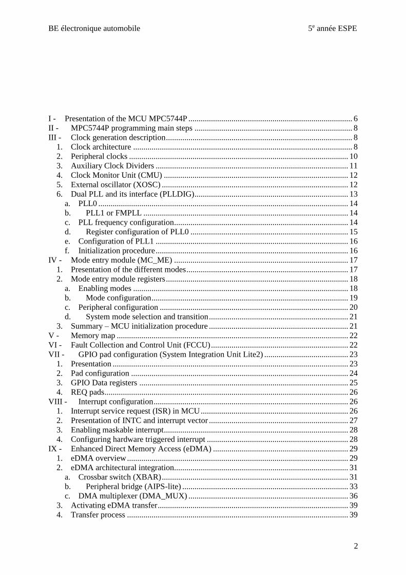
Figure 3 summarizes the limitation of the different bus clocks. They are required to maintain
synchronization between the different branches of the clock system. Any incorrect
configuration may result in failure or unpredictable behavior.
Figure 3 – System clock limitation (MPC5744PRM.pdf - p. 339 – Table 13-2)
The pin PB[6] proposes as alternate function CLKOUT, for the external observation of the
system clock. The bit EN in the register CGM_OC_EN is set to enable the output clock (see p
138). The frequency of the output clock can be divided through the content of the register
CGM_OCDS_SC.
2. Peripheral clocks
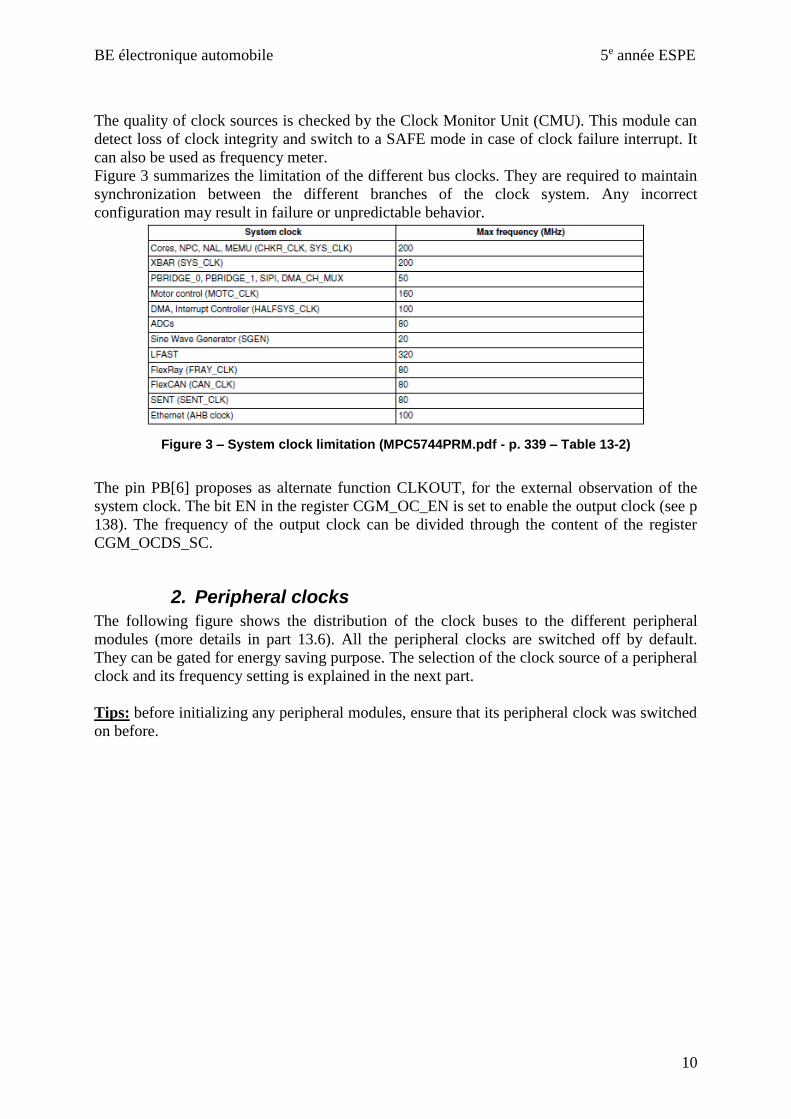
The following figure shows the distribution of the clock buses to the different peripheral
modules (more details in part 13.6). All the peripheral clocks are switched off by default.
They can be gated for energy saving purpose. The selection of the clock source of a peripheral
clock and its frequency setting is explained in the next part.
Tips: before initializing any peripheral modules, ensure that its peripheral clock was switched
on before.

BE électronique automobile 5e année ESPE
11
Figure 4 – Clock distribution (MPC5744PRM.pdf - p. 347 – Figure 13-3)
3. Auxiliary Clock Dividers
One of the purpose of the block MC_CGM is the generation of peripheral clocks. Typically,
three registers are related to the control of the auxiliary clocks:
▪ ACn_SC: clock source select between IRC, XOSC, PLL0 and PLL1
▪ ACn_SS: status of the clock source selection (read only)
▪ ACn_DC: activation and configuration of the divider of the auxiliary clock. The
division is equal to DIV+1. The write access to DIV is enabled only if DE is set. Byte
and half-word write accesses are not allowed for this type of register.

BE électronique automobile 5e année ESPE
12
The MC_CGM generates the following peripheral clocks (refer to Table 13-1 p 338):
▪ PBRIDGE0/1_CLK - controlled by CGM_SC_DC0 register
▪ Motor Control clock - controlled by the CGM_AC0_DC0 register
▪ SGEN clock - controlled by the CGM_AC0_DC1 register
▪ ADC clock - controlled by the CGM_AC0_DC2 register
▪ FlexRay clock - controlled by the CGM_AC1_DC0 register
▪ SENT clock - controlled by the CGM_AC1_DC1 register
▪ CAN clock - controlled by the CGM_AC2_DC0 register
▪ LFAST PLL clock - controlled by the CGM_AC5_DC0 register
▪ CLKOUT pin clock - controlled by the CGM_AC6_DC0 register
▪ ENET clock - controlled by the CGM_AC10_DC0 register
▪ ENET TIME clock - controlled by the CGM_AC11_DC0 clock register
Moreover, MC_CGM controls the selection of clock sources for PLL0 and PLL1:
▪ PLL0 - clock source selected by the MC_CGM_AC3_SC register
▪ PLL1 - clock source selected by the MC_CGM_AC4_SC register
4. Clock Monitor Unit (CMU)
Five Clock Monitor Units (CMU) are placed on clock buses in order used to test their
integrity and make sure that their frequencies stay within necessary operating limits. They act
as frequency meter, with IRCOSC used as clock monitor reference. For all safety critical
clocks, the microcontroller detects a missing clock or incorrect frequency.
If any of the five CMU detects an issue with the clock signal that is being monitored, an
interrupt or system reset could be generated, depending on how the CMUs are configured.
Each CMU is programmed independently. The reaction of the MCU to a clock loss depends
on the configuration of the FCCU.
Table 13.6 p 351 lists the monitored clocks by the different CMU.
Figure 5 – Monitored clock by the CMU (MPC5744PRM.pdf - p. 351 – Figure 13-6)
5. External oscillator (XOSC)
Refer to Part 13.5.2 and Chapter 28 for more information about FXOSC and its configuration.
This on-chip oscillator uses 8 MHz to 44 MHz crystal inputs. It can provide a clock source for
the system clock, both PLL and the different peripheral clocks. The energy management, the

BE électronique automobile 5e année ESPE
13
activation and the selection of XOSC as system clock are controlled by the mode entry
MC_ME module.
The only register which controls the XOSC is XOSC_CTL (p 841). OSCBYP controls the
bypass of the oscillator, EOCV counter specifies the duration for oscillator stabilization
checking. The interrupt linked to XOSC clock failure is enabled by the bit M_OSC. The flag
bit I_OSC indicates if an oscillator clock interrupt is pending. It must be cleared by writing a
‘1’.
After reset, XOSC is placed in powerdown mode. Its switch on is controlled by software
through the MC_ME module (ME_<mode>_MC register, XOSCON bit). The availability of a
stable oscillator clock is indicated by the status bit S_XOSC in the register ME_GS of the
MC_ME module.
6. Dual PLL and its interface (PLLDIG)
Refer to Part 13.5 and Chapter 25 for more information about dual PLL systems. The PLL
system in the MPC5744P is a dual PLL that provides separate system and peripheral clocks.
The dual PLL system is composed of PLL0 and PLL1 analog blocks and the digital interface
(PLLDIG) for PLL configuration. The two analog PLL blocks are cascaded, with the PHI1
output of PLL0 feeding the clock input of PLL1. The PHI0 output of PLL0 can serve as clock
source for the core or the peripheral clocks. With such an architecture, two clock sources with
independent frequencies can be used to drive peripherals and system core. While PLL0 is
non-modulated, PLL1 can be modulated for EMI reduction purpose.
The overall architecture of the dual PLL system is described in Figure 6. The PLLs are
disabled after power on and must be enabled by software:
▪ PLL0 is the primary PLL. This PLL is used to source a non-Frequency Modulated
clock to the MPC5744P modules and also the reference clock to PLL1.
▪ PLL1 is a Frequency Modulated PLL (FMPLL) that is typically used to drive the
system clock. PHI is the output of PLL1 which drives the System Clock Selector and
AUX Clock Selector 6 of the MC_CGM.

BE électronique automobile 5e année ESPE
14
Figure 6 – Block diagram of the PLL (MPC5744PRM.pdf - p. 341 – Fig. 13-2)
a. PLL0
The possible input clock sources for PLL0 are the XOSC, IRCOSC, and EXTAL Bypass. The
EXTAL Bypass input is the EXTAL pin. AUX Clock Selector 3 selects which input clock
will be used as the source for PLL0. The output clocks from PLL0 are PHI and PHI1. The
PHI output clock drives various peripheral clocks and the system clock when selected in the
MC_CGM. The PHI1 output provides one of the input references for PLL1.
b. PLL1 or FMPLL
The possible input clock sources for PLL1 are XOSC, PLL0_PHI, and EXTAL Bypass. The
EXTAL Bypass input is the EXTAL pin, which "bypasses" the XOSC output. AUX Clock
Selector 4 selects which input clock is used as the source for PLL1. The selection between
XOSC and EXTAL Bypass is made via the XOSC_CTL register of the XOSC module. The
output clock from PLL1 is the PHI clock, which can drive the system clock if the System
Clock Selector of the MC_CGM is configured to do so. The PHI output clock contains a
fractional divider that can be applied to the loop divide of the PLL to achieve good granularity
in the PLL1 PHI output clock frequency.
c. PLL frequency configuration
Except for the frequency modulation, the configuration of both PLL is quite similar. Figure 7
gives an overview of both PLL block diagram and the register to set their frequencies.
MFD
PREDIV
RFDPHI1
RFDPHI
RFDPHI
MFD
MC_CGM.AC3_SC.SELCTL
MC_CGM.AC4_SC.SELCTL
Figure 7 – Block diagram of both PLL and the register for frequency setting

BE électronique automobile 5e année ESPE
15
The relationship between input and output frequency is determined by programming the
PLL0DV, PLL1DV, and PLL1FD registers, and calculated according to the following
equations:
The relationship between the VCO frequency (fVCO) and the output frequency of the PLLs is
determined by the configuration of the PLL1DV, PLL1FD, and PLL0DV registers, according
to the following equations:
The frequency setting depends on the configuration of several registers, which must be done
carefully. PLL and VCO inputs and outputs must lie within frequency ranges to ensure a
correct operation. Any incorrect settings may lead to an unpredictable failure. PHI and PHI1
of PLL0 ranges are 4.76 - 200MHz and 20 - 156 MHz respectively. PLL1 output range is 4.76
- 200MHz. PLL0 input clock range is 8 - 40 MHz, while PLL1 input clock range is 38 - 78
MHz. When programming the PLLs, user software must not violate the maximum system
clock frequency or max/min VCO frequency specification of PLL0 and PLL1 (between 600
and 1250 MHz). Furthermore, the PLL0DV[PREDIV] value must not be set to any value that
causes the input frequency to the phase detector of analog PLL blocks to go below the
prescribed ranges.
d. Register configuration of PLL0
The input clock is selected by the auxiliary selector 3, through the field SELCTL of register
MC_CGM.AC3_SC and can be provided by either the IRC oscillator (SELCTL = 0) or
XOSC quartz oscillator (SELCTL = 1). The frequency setting for outputs PHI and PHI1
depends on the configuration of several dividers, defined in the register PLL0DV. The divider
names are the same as those used in the block diagram shown in Figure 7:
▪ PREDIV defines the division factor of the input clock of PLL0 (from 1 to 7).
▪ MFD defines the loop multiplication factor divider (from 8 to 127)
▪ RFDPHI and RFDPHI1 define the frequency dividers on PHI (from 1 to 63) and PHI1
(from 4 to 15) outputs
PLL0DV can be modified at anytime, but the changes become effective only after the PLL is
disabled and then re-enabled. If these fields are changed without powering down the PLL, the
PLL will lose lock and generate either a reset or interrupt based on which is enabled.

BE électronique automobile 5e année ESPE
16
Two interrupts are related with PLL0: loss of clock and loss of lock. They can be enabled
through the bits LOLIE and LOCIE in register PLL0CR. The status of related flags are given
by PLL0SR register.
The activation of the PLL0 by the bit PLL0ON in MC_ME.RUNx_MC register (see part IV).
e. Configuration of PLL1
The configuration of PLL1 is very similar to PLL0, except the clock source and the frequency
settings. The input clock is selected by the auxiliary selector 4, through the field SELCTL of
register MC_CGM.AC4_SC. It can be either the XOSC quartz oscillator (SELCTL = '01') or
PLL0_PHI1 output (SELCTL = '11').
The frequency settings depend on two registers: PLL1DV and PLL1FD. In PLL1DV, the
values of the reduced frequency divider (RFDPHI) and loop multiplication factor divider
(MFD) can be modified at anytime, but the new values only become effective after the PLL is
disabled, then re-enabled.
▪ MFD defines the loop multiplication factor divider (from 16 to 34)
▪ RFDPHI define the frequency divider on PHI output (from 1 to 63).
The frequency of PLL1 output can be finely tuned by enabling a fractional divider, set by
register PLL1FD. The fractional divider is enabled by the bit FD_EN and the division factor
is defined by the field FRCDIV.
The activation of the PLL1 by the bit PLL1ON in MC_ME.RUNx_MC register.
f. Initialization procedure
From RESET state, PLL0 and PLL1 are disabled. The initialization procedure is explained in
part 13.5.1.4 - p 343 of the reference manual.

BE électronique automobile 5e année ESPE
17
IV - Mode entry module (MC_ME) This block controls the different modes of the MCU and the transition sequences between the
different modes. The notions of modes and transitions between modes are essential to
configure the MCU correctly and initiate the user mode, which the normal operation mode.
Refer to Chapter 59 – Mode entry module for more details about the MPC5744P modes.
1. Presentation of the different modes
The MCU proposes different modes corresponding to different usages (system configuration
and monitoring, user mode, low power modes…). The embedded software executes only in
DRUN, SAFE, TEST and RUN0..RUN3 modes. RESET, DRUN, SAFE and TEST modes are
system modes. They are dedicated to the configuration and the monitoring of the system.
RUN0..RUN3, HALT0, STOP0 and STANDBY0 are user modes. HALT0, STOP0 and
STANDBY0 are low power modes. In the next chapter (Wakeup Unit), the procedure to exit
these low power modes will be detailed. The configuration of the MCU mode depends on the
requirements in term of energy management and processing power. Figure 8 presents a state
diagram of the microcontroller modes and the possible transitions.
▪ RESET: the application is not active, the chip configuration is initialized. The system
enters in this mode after a reset.
▪ DRUN: entry mode for the embedded software. It enables the configuration of the
system at the start-up. This is the only mode entry to a user mode. If the embedded
software does not enable a transition between DRUN mode and a user mode, the main
program defined by the user cannot execute. The system enters in this mode after the
end of Reset mode, and after software request from RUN0..RUN3, SAFE, TEST
modes, and a wake up request from STANDBY mode.
▪ SAFE: the system enters in this mode after the detection of a recoverable error. The
system exits this mode after a reset or DRUN from software (refer to part XVII of this
document - FCCU for details about configuration of the MCU to errors).
▪ TEST: for device self-test. The system enters in this mode from DRUN mode by
software request. The system exits this mode after a reset or by software request to
come back in DRUN mode.
▪ RUN0 .. RUN3: these are the embedded software modes where most processing
activity is done. 4 RUN modes are provided to enable different power and clock
configuration. The system enters in one of these modes after DRUN by software
request, interrupt event from HALT0, interrupt or wake up event from STOP0. The
system exists one of these modes after reset, entry in SAFE mode after an hardware or
software error, HALT0, STANDBY0 or STOP0 by request.
▪ STOP0: Reduced activity low power mode. The wakeup signals are processed rapidly,
contrary to HALT mode. By default, system clock is FIRC, but it can be switched off.
The data and flash memories are powered down but can be activated; the main
regulator is switched on. See chapter Wakeup Unit for more details about the exit of
STOP0 mode.

BE électronique automobile 5e année ESPE
18
▪ HALT0: Reduced activity low power mode. The clock core is disabled. The analog
peripherals can be switched off. The system enters in this mode by software request
from RUN0..RUN3 modes. The systems leaves this mode after a reset, after a
hardware or software failure to go in SAFE mode, or interrupt event to come back in
previous RUN0..RUN3 modes. Contrary to STOP0 and STANDBY0 modes, wakeup
signals cannot be used to exit from HALT0 mode.
▪ STANDBY0: This is the lowest power mode which ensures a reduced leakage current.
Most of the blocks of the MCU are switched off from the power supply to reduce
leakage current. Wake up from this mode is quite long. The system enters in this mode
by software request from DRUN, RUN0..RUN3 modes. The system leaves this mode
after reset, of after wake-up event to enter in DRUN mode (see chapter Wakeup Unit).
The wakeup from STANDBY0 mode is longer than from STOP0 mode. All the pins
are in high impedance mode. Only the reset generation mode, power control unit,
wake up unit, 8K RAM, RTC/API, CAN sampler, IRC and XOSC are powered.
Figure 8 – Mode entry diagram and possible mode transitions (MPC5744PRM.pdf - p. 2386– Fig. 59-2)
2. Mode entry module registers
a. Enabling modes
The Mode Enable Register ME allows enabling or disabling some MCU modes (except
RESET, DRUM, SAFE and RUN0).

BE électronique automobile 5e année ESPE
19
b. Mode configuration
A mode configuration register is associated to each mode to control the connection or
disconnection of some peripherals in the mode, such as the I/O output buffers, internal voltage
regulator, data and code flash memory, PLL, fast external crystal and RC oscillators. It
specifies also the system clock (SYSCLK) used by the system (PLL, crystal oscillator, fast
RC oscillator…). All these registers have the same structure. The following figure shows the
register structure for RUN0 .. RUN3 mode configuration registers, called RUN[0] to RUN[3].

BE électronique automobile 5e année ESPE
20
c. Peripheral configuration
Up to eight different behaviors can be configured for the peripherals of the MCU in the
different run modes. These 8 behaviors are defined by the Run Peripheral Configuration
Registers 0 to 7 (RUNPC[0] to RUNPC[7]).
Setting a bit associated to a mode to ‘0’ means that, if this configuration is given to a
peripheral, this peripheral will be frozen in with clock gated during this mode. If this bit is set
to ‘1’, the peripheral will be active. For example, let’s suppose that we define one behavior in
RUNPC[0] and we write 0x00000030. If this configuration is associated to one peripheral,
this peripheral will be active only in RUN0 and RUN1 mode. In all other modes, it will be
frozen.
For the low power modes HALT0 and STOP0, 8 behaviors can also be configures through the
registers Low Power Peripheral Configuration LPPC[0]to LPPC[7].
Once the different possible behaviors have been configured with registers RUNPC and LPPC
registers, these behaviors can be associated to the peripherals of the MCU. 32 registers called
Peripheral Control Registers PCTL[9]to PCTL[255] are associated to each peripheral. These
registers contains 3 fields: the field RUN_CFG defines which one of the 8 behaviors defined
in RUNPC[0] to RUNPC[7] will be associated to the peripheral during the run modes. The
field LP_PC defines which one of the 8 behaviors defined in LPPC[0] to LPPC[7] will be
associated to the peripheral during the non run modes. The bit DBG_F sets the behavior of the
peripheral in Debug mode.
The status of the peripherals is given by the registers PS0, PS1, PS2 and PS3.
Remark: to find the correct PCTL register associated to one peripheral, refer to the memory
map of the ME module (Table p 2291, the PCTL register can be found at the end of the table).
For example, the register PCTL[237] is associated to the ADC0 block, the register PCTL[255]
is associated to the module PWM0.

BE électronique automobile 5e année ESPE
21
d. System mode selection and transition
The Mode Control Register MCTL is used to trigger mode change by software. The
TARGET_MODE field defines the target mode to be entered by software request.
The KEY field is a control key to enable the writing in this register. The KEY is 0x5AF0. A
different value is invalid and any writing in the register will be ignored. Actually, two writing
of the register have to be done to force the device to enter in the mode defined by
TARGET_MODE: first time with the good value of the key, a second time with the inverted
value of the key. For example, suppose that we want the system to exit DRUN mode to enter
RUN0 mode. The TARGET_MODE field must be equal to ‘0100’. Therefore, the two
following lines have to be written in the software:
MC_ME.MCTL.R= 0x40005AF0; /* Enter the target mode and the Key */
MC_ME.MCTL.R= 0x4000A50F; /* Enter the target mode and the inverted Key */
The global mode status of the system is given by the register Glogal Status Register GS. The
field S_CURRENTMODE notifies the current device mode. The bit S_MTRANS notifies if a
mode transition is on-going. It gives also the status of several MCU peripherals.
3. Summary – MCU initialization procedure
The procedure to initialize the MCU is always the same and describes below. This procedure
must be done in DRUN mode.
1. Enables the modes to be used

BE électronique automobile 5e année ESPE
22
2. Configure the clock sources
3. Configure the modes to be used
4. Configure the peripherals
5. Switch from DRUN mode to a user mode (RUN0,1,2,3)
Tips: in case of lack of operation of one peripheral, ensure that it has been enabled in the
current running mode. If it is not the case, the peripheral is frozen.
V - Memory map The memory map of the MPC5744P is described in Chapter 5 of the reference manual. The
addressing is done at the octet level. Before any write/read operation in the memory, ensure
that it is not done in a reserved area. Any operation in a reserved area of the memory may lead
to a degraded and unpredictable operation.
For example, the system RAM, which is dedicated for embedded program, is located between
address 0x40000000 and 0x4005FFFF. You cannot use this part of the memory to store data.
In contrary, the address region between 0x50800000 and 0x5080FFFF , which is called D-
MEM CPU0, is a 64 kBytes area to store data.
VI - Fault Collection and Control Unit (FCCU) Refer to chapter 69 - Fault Collection and Control Unit (FCCU).
The Fault Collection and Control Unit (FCCU) offers a hardware channel to collect faults and
to place the device into a safe state when a failure in the device is detected. No CPU
intervention is requested for collection and control operation.
Collect faults and configurable fault control and reaction.
Main features:
Management of non-critical faults
• HW or SW fault recovery management
• Fault detection and collection
• Fault injection (fake faults)
• External reaction (fault state): EOUT signalling. Error indication via the pin(s) is
controlled by the FCCU.
• Internal chip reactions (alarm state): interrupt request
• Internal chip reactions (fault state):
• long functional reset request pulse
• short functional reset request pulse
• NMI
• Bi-Stable, Dual-Rail and Time Switching output protocols on EOUT
• Internal (to the FCCU) watchdog timer for the reconfiguration phase
• Configuration lock

BE électronique automobile 5e année ESPE
23
Two pins sent to SBC: EOUT[0] and EOUT[1] (Error Output—Indicate to off-chip logic that
a fault has occurred).
Dual core operation: transparent for the programmer. The only thing to do is to configure the
FCCU.
VII - GPIO pad configuration (System Integration Unit Lite2)
Refer to Chapter 16 – System Integration Unit Lite for the configuration of General Purpose
I/O (GPIO) pads and the multiplexing of alternate functions associated to GPIO. Refer also to
chapter 4 for the signal description and the pin-out of the MPC5744P according to the
package version.
1. Presentation
The microcontroller MPC5744P may support up to 32 ports of 16 I/O pads, i.e. 512 pads. In
practice, only 10 ports (port A to J) are provided. Depending on the package, some pins may
be removed. The I/Os of the microcontroller are supplied under 3.3 V, so I/Os support only 0-
3.3 V signal !
All the pad can be configured independently through the pad configuration registers. Two
different pad configuration registers exist for each pad to multiplex the which source signal is
connected to the register's associated destination (input or output buffer of the pad):
▪ the register Multiplexed Signal Configuration Register (MSCR[n] with n from 0 to
263) for multiplexing from on-chip module to the pad output buffer
▪ the register Input Multiplexed Signal Configuration Register (IMCR[n]) for
multiplexing from the pad input buffer and the on-chip module

BE électronique automobile 5e année ESPE
24
The number of the MSCR and IMCR register related to a given pad can be found in table 4.7
p 107 or table 4.16 p 151 of the reference manual. Be careful, the number associated to
MSCR and IMCR for the same pad are different !
For example, the pad PA[0] is associated to the register MSCR[0], but three different IMCR
are related to PA[0]: IMCR[48], IMCR[59] and IMCR[173].
One input register GPDI and one output register GPDO are associated to each pad. 15 GPIO
are associated to External Interrupt Request (EIRQ) pins (EIRQ[0:15]). They can trigger
interrupt on rising edge or falling edge events, depending on the configuration of registers
SIUL_IREER and SIUL_IFEER. Some glitch filter can be configured at the input of these
pins.
2. Pad configuration
Most of the pad configuration is related to MSCR register. MSCR also controls the routing of
source signals from various on-chip module to one I/O pad. The routing of a signal from I/O
pads to an on-chip module is controlled by the peripheral input multiplexing register: IMCR
register. Figure 9 illustrates the connection between on-chip module and input/output buffer.
Figure 9 – Multiplexing between on-chip module and input/output buffer of I/O pad (MPC5744PRM.pdf - p. 497– Fig. 16-2)
MSCR[n] registers controls:
▪ the activation of input and output buffers (bits IBE and OBE)
▪ the activation of the analog pad (bit APC, required when the signal is routed to an
analog block)
▪ the activation of pull-up or pull-down devices
▪ the slew rate and drive of the I/O (SRC fields). Full drive without slew rate control is
required for high speed I/O. For EMI reduction purpose, it is required to use reduced
drive with slew rate control for I/O without high speed constraints.
▪ the source signal (up to 4) through the field SSS.
The details of multiplexing associated to each IMCR registers can be found in part 4.3.6 of
the reference manual (p. 136).

BE électronique automobile 5e année ESPE
25
Tips : if an I/O pad is used as an output, the bit OBE must be set to '1' and the bit IBE to '0'. If
the I/O pad is used as an input, the bit OBE must be set to '0' and the bit IBE to '1'.
Tips : the list of pins with analog functions can be found in part 4.3.7 of the reference manual
(p. 148).
3. GPIO Data registers
The logical status of I/O pads can be accessed at pad level, but also at port level. Here, the
different methods to read or write I/O pads are described.
The data are written on individual output pads by the bit PDO of the registers GPDO[n], n = 0
to 263, where n is the MSCR number associated to the pad. The data are read from individual
input pads by the bit PDI of the registers GPDI[n], n = 0 to 263.
The I/O pads are mapped into ports of 16 I/O pads. I/O ports can be accessed in parallel mode
with registers PGPDO and PGPDI for writing and reading direction respectively.
Figure 10 – Mapping of I/O ports to PGPDO registers (MPC5744PRM.pdf - p. 149– Table 4-12)
Figure 11 – Mapping of I/O ports to PGPDI registers (MPC5744PRM.pdf - p. 149– Table 4-13)

BE électronique automobile 5e année ESPE
26
It is also possible to write on output ports through a mask, defined by the registers
MPGPDO[n]. Each 32 bit register is associated to one port. The 16 most significant bits of the
register define the mask (field MASK). The 16 least significant bits define the data to be
written on the output buffer (field MPPDO).
4. REQ pads
32 GPIO are also defined as external interrupt request input pins, called REQ[n], n from 0 to
31. Any rising or falling edge events applied on these input pads can trigger maskable
interrupts. Four interrupts request are associated to REQ pads (SIUL2 External Interrupt 0 to
3, vectors 243 to 246). The 8 first REQ pads are associated to the first interrupt request vector
while the 8 last EIRQ are associated to fourth interrupt request vector.
The interrupt request associated to each EIRQ input can be individually enabled by the
register DIRER0. The reaction of the MCU to external interrupt request can be either a direct
memory access (DMA) or an interrupt, depending on the configuration of DIRSR0.
Each time an interrupt is pending, the flag bit EIF of the register DISR0 is set to ‘1’. Writing a
‘1’ clears the flag. Interrupt can arise on rising and/or falling edge events on REQ pins. It can
be configured by the registers IREER0 and IFEER0.
Noise coupled on input pins can induce glitches that may be misread as a rising or falling
edge. Therefore, digital glitch filter can be enabled on each REQ inputs, by setting bits IFE in
IFER0 register. The digital glitch filters are configured by the registers IFMCR and IFCPR.
VIII - Interrupt configuration Refer to Chapter 21 – Interrupt Controller (INTC) for the configuration of priority of the
different interrupt source.
1. Interrupt service request (ISR) in MCU
All the real-time controllers in interaction with their environment operate by interruption of
their on-going program. The execution of functions depends on external events (e.g. pushed
button, detection of a voltage above a given threshold, reception of a signal…). The interrupt
service requests (ISR) are predefined and associated either to hardware peripherals, resets or
software requests. When the conditions for the triggering of an interrupt are detected by the
CPU, the execution of a function dedicated to the ISR processing can launched, depending on
the interrupt configuration (interrupt enabled or not if the interrupt is maskable), the content
of interrupt vector table and the level of priority of the ISR.
The interrupt vector table is an area of the memory divided in interrupt vectors. Each interrupt
vector has a fixed memory address and is associated to a given ISR (e.g. edge detection on an
input digital buffer or time-out of a timer). At the address of the interrupt vector, the memory
contains the address of the function dedicated to the processing of the ISR (for example, when
an edge is detected on an input digital buffer, the programmer wants to launch a program that
switch on an external LED). The programmer must know exactly the address of interrupt
vector in order to associate an ISR to the execution of a processing function.
When an ISR is triggered during the execution of the main program, the address of the next
instruction of the main program must be saved, in order to come back to the main program
after the processing of the interrupt. In practice, before stopping the execution of the main
program and launch the interrupt program, the content of the program counter is saved and
will be updated at the end of the interrupt program.
BE électronique automobile 5e année ESPE
27
The interrupt management is complex and is done by an interrupt controller (INTC) which
aims at scheduling the ISR, i.e:
▪ Notifying the CPU that an ISR is transmitted by a peripheral or the software
▪ Managing the priorities between the different incoming ISR
▪ Transmitting to the CPU the address of the program to process the interrupt
2. Presentation of INTC and interrupt vector
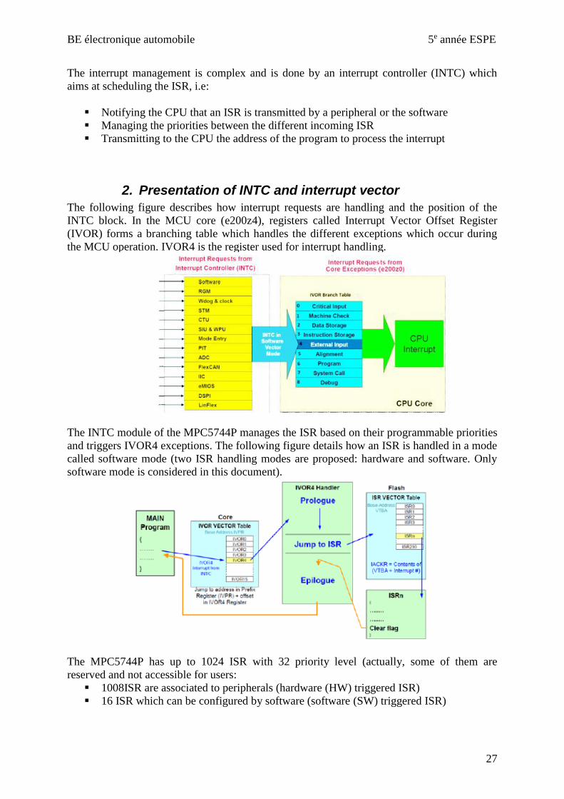
The following figure describes how interrupt requests are handling and the position of the
INTC block. In the MCU core (e200z4), registers called Interrupt Vector Offset Register
(IVOR) forms a branching table which handles the different exceptions which occur during
the MCU operation. IVOR4 is the register used for interrupt handling.
The INTC module of the MPC5744P manages the ISR based on their programmable priorities
and triggers IVOR4 exceptions. The following figure details how an ISR is handled in a mode
called software mode (two ISR handling modes are proposed: hardware and software. Only
software mode is considered in this document).
The MPC5744P has up to 1024 ISR with 32 priority level (actually, some of them are
reserved and not accessible for users:
▪ 1008ISR are associated to peripherals (hardware (HW) triggered ISR)
▪ 16 ISR which can be configured by software (software (SW) triggered ISR)

BE électronique automobile 5e année ESPE
28
Refer to Table 7-16 p 193 for the list of available ISR and the number of interrupt vector
associated to an interrupt source. For example, interrupt request triggered by time-out of
module Timer channel 0 (PIT_0) is associated to interrupt vector 226.
Tips: when you develop embedded code project with S32DS IDE, the list of interrupt vectors
can be found in the file intc_SW_mode_isr_vectors_MPC5744P.c, which is automatically
added in the project.
SW triggered ISR are dedicated to:
▪ In a multiprocessor context, interruption of a processor activity by another processor
▪ In a program launched by a high level ISR, if a part of the program has a lower level
priority, it is possible to suspend the execution of this part by a software ISR. It
improves the management of dead-lines of operation.
The priority of each ISR can be configured, with a level from 0 (lowest priority) to 31
(highest priority). Most of the HW triggered interrupts are maskable, i.e. it is possible to
inhibit the ISR transmission to the INTS by the peripheral, by setting an interrupt enable bit
(see configuration registers of each peripheral to know how to mask interrupt). Each time an
ISR is launched, a flag bit is set. One flag bit is associated to one ISR source. The flag bits are
in interrupt flag registers associated to the peripherals.
In order to associate an ISR coming from a peripheral or the software and a program to
process the ISR, an interrupt handler has to be defined. This interrupt handler writes the
address of the interrupt processing program at the interrupt vector address, and manages the
ISR priority. We will see how to deal with interrupt handler with hardware or software ISR in
the MPC5744P.
3. Enabling maskable interrupt
Maskable interrupt must be enabled at two levels: at local level (i.e. at peripheral level) by a
interrupt enable bit associated to ISR source, and at global level. In project developed with
S32DS, in order to enable ISR in the MCU, you can execute this routine in your program:
xcptn_xmpl ()
This function is defined in the source file MPC57xx__Interrupt_Init.c, which is automatically
added in a new project. This function initializes INTC and enable interrupt at global level.
4. Configuring hardware triggered interrupt
HW triggered interrupts are most of the time maskable interrupts, so the peripheral
configuration must enable ISR and the maskable interrupt must enabled at global level. INTC
configuration routines are implemented in several files: vector.c, MPC57xx__Interrupt_Init.c
and intc_SW_mode_isr_vectors_MPC5744P.c. They contain the routines used to execute the
ISR handling procedure.
In order to configure the interrupt handler, two operation must be done:
▪ 1. associate a ISR vector to an ISR routine, i.e. the user-defined function that will be
called when the interrupt is triggered.
▪ 2. define the priority level of the ISR

BE électronique automobile 5e année ESPE
29
In project developed in S32DS, the link between the ISR routine and the ISR vector can be
done in the file intc_SW_mode_isr_vectors_MPC5744P.c, which lists all ISR vectors. Here is
an example with ISR related to Timer module PIT_0:
(uint32_t) &dummy, /* Vector # 226 Periodic Interrupt Timer (PIT_0) channel 0 PIT_0 */
(uint32_t) &dummy, /* Vector # 227 Periodic Interrupt Timer (PIT_0) channel 1 PIT_0 */
(uint32_t) &dummy, /* Vector # 228 Periodic Interrupt Timer (PIT_0) channel 2 PIT_0 */
(uint32_t) &dummy, /* Vector # 229 Periodic Interrupt Timer (PIT_0) channel 3 PIT_0 */
In the default configuration, the function dummy is called each time an ISR related to PIT_0 is
triggered. As its name indicates, this function defined in the file
intc_SW_mode_isr_vectors_MPC5744P.c does nothing in particular. Let suppose that you
enable the ISR related to time-out of PIT_0 channel 0 and that you have defined an ISR
routine PIT0_Ch0_isr, change the line associated to vector 226 in the following way:
(uint32_t) &PIT0_Ch0_isr, /* Vector # 226 Periodic Interrupt Timer (PIT_0) channel 0 PIT_0
*/
The priority level of each ISR source can be configured with the register PSR[n] of INTC,
where n is the number of the interrupt vector.
IX - Enhanced Direct Memory Access (eDMA) Refer to chapter 22 for details about eDMA and to chapter 23 for DMA multiplexer
(DMA_MUX). Refer also to part 7.4.7 for integration of DMA within the system. When
DMA transfer concerns peripheral, some architectural principles about memory access in
Power architecture are required. This chapter will also provide some details about the crossbar
switch (XBAR) and the peripheral bridges (AIPS). Information about crossbar switch is
available in chapter 17 and also in part 7.4.7 for its architecture. Refer to chapter 19 for
information about peripheral bridge and part 7.4.5 for its architecture.
1. eDMA overview
eDMA is a DMA controller, which aims at managing memory transfer without CPU
intervention. Once configured and initiated, the DMA controller operates in parallel to the
Central Processing Unit (CPU), performing data transfers that would otherwise have been
handled by the CPU. This results in reduced CPU loading and a corresponding increase in
system performance. In a motor control application, DMA can be beneficial: numerous
analog-to-digital conversion are launched and data are transferred regularly to off-chip circuit
(e.g. MOS driver, speed/position sensors). Without DMA, CPU must initiate the data
read/write operation of ADC results and communication data. With DMA, the intervention of
CPU is not necessary to initiate the transfer. In Figure 12, DMA is illustrated through an
example of a source data writing in the transmission buffer of SPI bus.

BE électronique automobile 5e année ESPE
30
Figure 12 - Illustration of DMA principle (from Freescale AN4765 - MPC57xx: Configuring and Using the eDMA Controller)
MPC5744P implements two 32-channel DMA controllers: DMA_0 and DMA_1. DMA_1 is
implemented in delayed lockstep and is not visible to software. A DMA channel manages the
data transfer from one memory location to another. Each DMA channel is configurable by the
user. The DMA arbitrates channel service requests in two groups of 16 channels each:
▪ Group 1 contains channels 31-16
▪ Group 0 contains channels 15-0
DMA can be initiated from two request sources:
▪ software request, i.e. from a CPU request
▪ hardware request, from a peripheral.
As it will be explained in the following part, for software request, DMA configuration is quite
simple. However, for hardware request, several parts of the system may be configured
(DMA_MUX, AIPS, XBAR). The DMA multiplexer (DMA_MUX) is extremely important. It
aims at connecting the DMA hardware request sources to the DMA channel. Without
configuration of DMA_MUX, the hardware request cannot reach the eDMA module.
This device contains two DMA_MUX modules. DMAMUX_0 connects directly to DMA
channels 0-15. DMAMUX_1 connects directly to DMA channels 16-31.
Each DMA channel can be independently configured with the details of the transfer sequence
that is to be executed. These details are specified in the channel Transfer Control Descriptor
(TCD) registers.
eDMA transfers can be activated in three ways:
▪ 1. Events occurring in peripheral modules and off-chip can assert a DMA transfer
request
▪ 2. Software activation
▪ 3. Channel-to-channel linking—on completion of a transfer, one channel activates
another
Each channel can generate interrupts to indicate that it has partially completed or fully
completed a transfer. Interrupts can also be generated to indicate that a transfer error has
occurred.

BE électronique automobile 5e année ESPE
31
2. eDMA architectural integration
Before explaining how to configure eDMA, it is necessary to give some explanation about
how memory access is managed in Power architecture microcontroller, especially when
attempt to read/write peripheral memory is done. Two modules are involved in this process:
the crossbar switch and the peripheral bridge.
a. Crossbar switch (XBAR)
To allow the eDMA, CPUs, and other masters to operate simultaneously, a multi-master bus
architecture is implemented in MPC5744P. The MPC57xx chips feature multiple bus masters:
for example, cores, Fast Ethernet Controller, and LFAST. The crossbar switch (XBAR) forms
the heart of this multi-master architecture. It links each master to the required slave device.
The crossbar switch connects bus masters and bus slaves using a crossbar switch structure, as
shown in Figure 13. This structure allows all bus masters to access different bus slaves
simultaneously, while providing arbitration among the bus masters when they access the same
slave. The multi-port Crossbar Switch concurrently supports up to 4 simultaneous connections
between master ports and slave ports. Data passes from one crossbar to the next if a master
requires access to a slave that is not on the same crossbar as itself.
If two or more masters attempt joint access to the same slave, an arbitration scheme
commences, eliminating the risk of bus contention. Both fixed-priority and round-robin
arbitration schemes are available.
Figure 13 - Multi-master bus architecture provided by the crossbar switch (from Freescale AN4765 - MPC57xx: Configuring and Using the eDMA Controller)
The Crossbar Switch provides the following features:
▪ Four master ports and five slave ports, given in the figure below. For example, eDMA
is the master number 5. PBRIDGE 0 and PBRIDGE 1 will be discussed in the next
part. They will give access to peripheral memory.
▪ 32-bit Address, 64-bit Data paths (applies to all ports) with misaligned access
signaling
▪ Concurrent transfers between independent master and slave ports
▪ Programmable arbitration priorities on a per-slave port basis
▪ Round-robin arbitration available on a per-slave port basis
▪ Parking on slave ports: explicit master, park_on_last_master, none (low power parking)

BE électronique automobile 5e année ESPE
32
Figure 14 - Crossbar switch integration (MPC5744PRM.pdf - p. 186 – Fig. 7-1)
The crossbar switch and interaction between bus masters and slave devices is illustrated in a
simplified version in the figure below. In this example, the eDMA controller is accessing one
of the peripherals on the IP bus while the CPU is concurrently accessing the SRAM memory.
The crossbar switch has formed the appropriate connections for this situation. Two scenarii
are illustrated:
▪ software request: the core sends a software DMA request to the DMA engine. The
DMA access to the SRAM memory as a master of XBAR switch. If the targeted data
corresponds to a memory location associated to peripheral, the peripheral bridge
(AIPS) serves as interface between the memory and the XBAR switch.
▪ hardware request: the hardware DMA request is directed to the DMA channel by the
DMA_MUX. As in the previous case, the DMA engine is the master of the XBAR
switch. As the peripheral request an access to its memory, AIPS must be configured to
authorize read/write access.

BE électronique automobile 5e année ESPE
33
When a master accesses the crossbar switch, the access is immediately taken. If the targeted
slave port of the access is available, then the access is immediately presented on the slave port.
Single-clock or zero-wait-state accesses are possible through the crossbar. If the targeted slave
port of the access is busy or parked on a different master port, the requesting master simply
sees wait states inserted until the targeted slave port can service the master's request. The
latency in servicing the request depends on each master's priority level and the responding
slave's access time.
Because the crossbar switch appears to be just another slave to the master device, the master
device has no knowledge of whether it actually owns the slave port it is targeting. While the
master does not have control of the slave port it is targeting, it simply waits.
Arbitration settings for the crossbar switch can be configured in the XBAR module registers.
When operating in fixed-priority mode, each master is assigned a unique priority level in the
priority registers (PRSn). If two masters request access to the same slave port, the master with
the highest priority in the selected priority register gains control over the slave port. If an
attempt is made to program multiple master ports with the same priority level within the
priority registers (PRSn), the crossbar switch responds with a bus error.
In most of cases, no initialization is required for the crossbar switch. By default, fixed-priority
mode is configured and default priority is given to the different master. Hardware reset
ensures all the register bits used by the crossbar switch are properly initialized to a valid state.
However, settings and priorities may be programmed to achieve maximum system
performance. It is outside the scope of this document.
b. Peripheral bridge (AIPS-lite)
The peripheral bridge (PBRIDGE or AIPS or IPS bus) modules are used to access the
registers of most of the modules on this device. The peripheral bridge functions as a bus
protocol translator between the crossbar switch and the slave peripheral bus. The peripheral
bridge manages all transactions destined for the attached slave devices and generates select
signals for modules on the peripheral bus by decoding accesses within the attached address
space.
This device contains two identical peripheral bridge instances (PBRIDGE0 or AIPS0, and
PBRIDGE1 or AIPS1). The peripheral bridge occupies 64 MB of the address space, which is
divided into peripheral slots of 16 KB. The bridge includes separate clock enable inputs for
each of the slots to accommodate slower peripherals.
Tips: the clocks PBRIDGE0_clk and PBRIDGE1_clk are dedicated to PBRIDGE0 and
PBRIDGE1. These clocks are derived from SYSCLK after a configurable prescaler. The
frequency of these clocks must not exceed 50 MHz.
The slave devices connected to the peripheral bridge are modules which contain a
programming model of control and status registers. The system masters read and write these
registers through the peripheral bridge. The register maps of the peripherals are located on 16
KB boundaries. Each peripheral is allocated one or more 16-KB block(s) of the memory map.
Each Peripheral Bridge's MPRA register (Master Privilege Register A) contains fields for
each Crossbar Switch master on the chip. It defines the access-privilege level associated with
a bus master in the device to various peripherals: master n trusted for read and/or write. By

BE électronique automobile 5e année ESPE
34
default, only accesses from master 0 (the core) have read and write privileges. Thus, in order
to give privilege to DMA to access to peripheral bridge, the register MPRA must be set.
The peripherals attached to the peripheral bridges each are assigned to a memory map slot that
corresponds to a peripheral bridge register field. Every on-platform peripheral has an assigned
PACRn field within the PACRA to PACRH registers, and every off-platform peripheral has
an assigned OPACRn field within the OPACRA to OPACRAF registers. These registers
define the access level supported by the module:
▪ Supervisor protect: Determines whether the peripheral requires supervisor privilege
level for accesses
▪ Write protect: Determines whether the peripheral allows write access
▪ Trusted protect: determines whether the peripheral allows accesses from an untrusted
master
In order to configure the privilege access to the memory associated to the different
peripherals, the peripheral slot assignment to the PACR and OPACR is required. The
following tables provide the peripheral slot assignments for this device.

BE électronique automobile 5e année ESPE
35

BE électronique automobile 5e année ESPE
36
For most off-platform peripherals (e.g. CTU, ADC, …), write accesses are allowed by default.
Thus, the default configuration can be used for DMA access to these peripheral registers.
c. DMA multiplexer (DMA_MUX)
The DMA multiplexer (DMA_MUX) performs the task of routing the peripheral DMA
request sources to the desired DMA channel of eDMA module. It also provides the ability to
gate a transfer request with the Periodic Interrupt Controller (PIT), on selected MUX
implementations.
The DMA multiplexer is used to route the numerous peripheral DMA sources to individual
DMA channels. The Direct Memory Access Multiplexer (DMAMUX) routes DMA sources,
called slots, to any of the 16 DMA channels. Up to 27 peripheral slots and up to six always-on
slots can be routed to 16 channels. 16 independently selectable DMA channel routers, with
the first four channels additionally provide a trigger functionality. Each channel router can be
assigned to one of the possible peripheral DMA slots or to one of the always-on slots.
There are three operation modes:
▪ disabled: the DMA channel is disabled (after reset or for reconfiguration). It may also
be used to temporarily suspend a DMA channel while reconfiguration of the system
takes place (for example, changing the period of a DMA trigger).
▪ normal: DMA source is routed directly to the specified DMA channel. The operation
of the DMAMUX in this mode is completely transparent to the system.
▪ periodic trigger mode: a DMA source may only request a DMA transfer, such as when
a transmit buffer becomes empty or a receive buffer becomes full, periodically.
Configuration of the period is done in the registers of the periodic interrupt timer (PIT).
This mode is available only for channels 0–3.
Figure 15 - DMA_MUX block diagram (MPC5744PRM.pdf - p. 740 – Fig. 23-1)

BE électronique automobile 5e année ESPE
37
The following tables define the mapping of the DMA_MUX source slots to the DMA
hardware request sources on the device.

BE électronique automobile 5e année ESPE
38
The DMA_MUX also provides a number of “always enabled” request sources that can be
used in periodic trigger mode. These permit transfers to be initiated based only on the PIT.
The DMA channel triggering capability allows the system to schedule regular DMA transfers,
usually on the transmit side of certain peripherals, without the intervention of the processor.
This trigger works by gating the request from the peripheral to the DMA until a trigger event
has been seen. After the DMA request has been serviced, the peripheral will negate its request,
effectively resetting the gating mechanism until the peripheral reasserts its request and the
next trigger event is seen. This means that if a trigger is seen, but the peripheral is not
requesting a transfer, then that trigger will be ignored.
Each of the DMA channels can be independently enabled/disabled and associated with one of
the DMA slots (peripheral slots or always-on slots) in the system, through the configuration of
Channel Configuration registers CHCFGn (n = 0..15).
Tips: Setting multiple CHCFG registers with the same source value will result in
unpredictable behavior. This is true, even if a channel is disabled (ENBL==0). Before
changing the trigger or source settings, a DMA channel must be disabled via
CHCFGn[ENBL].

BE électronique automobile 5e année ESPE
39
Configuration of the DMAMUX is intended to be a static procedure done during execution of
the system boot code. The configuration of the DMA_MUX can be changed during the
normal operation of the system.
3. Activating eDMA transfer
Events occurring within other peripheral modules can be enabled to activate eDMA transfers.
In many modules, event flags can be asserted as either eDMA or interrupt requests. Due to the
high number of sources for those requests, a configurable multiplexer (DMA_MUX) is
implemented to route peripheral DMA requests to DMA channels.
Channels may also be activated by software. The channels’ TCDs provide a START bit that
activates the channel when asserted. This makes it possible to activate each channel in
software.
Channel linking provides the means for one channel to assert the START bit of another
channel. The linked channel can be activated at stages of the transfer or on completion of the
transfer. More details about the transfer process are given in the next part.
4. Transfer process
a. Handling multiple transfer requests
Only one channel can actively perform a transfer at a given time. Therefore, to handle
multiple pending transfer requests the eDMA controller offers channel prioritization. Fixed-
priority or round-robin prioritization can be selected.
In the fixed-priority scheme, each channel is assigned a priority level. When multiple requests
are pending, the channel with the highest priority level performs its transfer first. By default,
fixed priority arbitration is implemented, with each channel being assigned a priority level
equal to its channel number. Other priority levels can be assigned if required. Higher priority
channels can preempt lower priority channels. Preemption occurs when a channel is
performing a transfer while a transfer request is asserted to a channel of a higher priority. In
this case, the lower priority channel halts its transfer and allows the channel of higher priority
to carry out its transfer. The lower priority channel then resumes its transfer when the higher
priority channel has completed its transfer. One level of preemption is supported. Preemption
is an option and must be enabled on a per-channel basis if required.
In round-robin mode, the eDMA cycles through the channels in order (from high to low
channel number), checking for a pending request and without regard to priority. When a
channel with a pending request is reached, it is allowed to perform its transfer. When the
transfer has been completed, the eDMA continues to cycle through the channels looking for
the next pending request.
Arbitration within each group (group 0 = channel 15-0 and group 1 = channel = 31-16) is set
according to fixed-priority or round-robin mode. The group priorities operate in a similar
fashion. In group fixed priority arbitration mode, channel service requests in the highest
priority group are executed first, where priority level 1 is the highest and priority level 0 is the
lowest. The group priorities are assigned in the GRPnPRI fields of the DMA Control Register
(CR). All group priorities must have unique values prior to any channel service requests
occurring; otherwise, a configuration error will be reported. For group round robin arbitration,

BE électronique automobile 5e année ESPE
40
the group priorities are ignored and the groups are cycled through (from high to low group
number) without regard to priority.
b. Major and minor transfer loops
During DMA transfer, data are sent by packets according to a scheme made of a certain
number of loops. Each time a channel is activated and executes, a number of bytes,
“NBYTES,” are transferred from the source to the destination. This is referred to as a minor
transfer loop. A major transfer loop consists of a number of minor transfer loops. This number
is specified within the TCD registers. As iterations of the minor loop are completed, the
current iteration counter (CITER) in TCD field is decremented. When the current iteration
field has been exhausted, the channel has completed a major transfer loop. Figure 16 shows
the relationship between major and minor loops. In this example, a channel is configured so
that a major loop consists of three iterations of a minor loop. The minor loop is configured to
be a transfer of 4 bytes.
Figure 16 - Major and minor loop transfer (from Freescale AN4765 - MPC57xx: Configuring and Using the eDMA Controller)
The channel performs a selection of tasks upon completion of each minor and major transfer
loop. On completion of the minor loop, excluding the final minor loop, the eDMA carries out
the following tasks:
▪ Each time source data is transferred, updating the source address by adding the current
source address to the signed source offset: SADDR = SADDR + SOFF. Source
address is updated automatically as transfers are performed. On completion of the
minor loop, the source address contains source address for the last piece of data that
was read in the minor loop; offset is added to this value.
▪ Updating the destination address by adding the current destination address to the
signed destination offset: DADDR = DADDR + DOFF. It is done in a similar way as
source address updating.
▪ Decrementing the current iteration (CITER) counter
▪ Updating channel status bits and requesting (enabled) interrupts
▪ Asserting the start bit of the linked channel upon completion of minor loop, if channel
linking is enabled
On completion of the major/final minor loop, the eDMA performs the following tasks:
▪ Updating source address by adding the current source address to the last source
address adjustment: SADDR = SADDR + SLAST
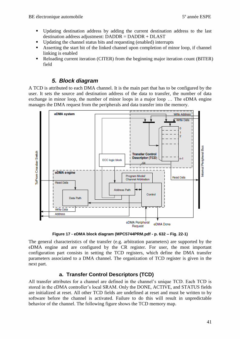
BE électronique automobile 5e année ESPE
41
▪ Updating destination address by adding the current destination address to the last
destination address adjustment: DADDR = DADDR + DLAST
▪ Updating the channel status bits and requesting (enabled) interrupts
▪ Asserting the start bit of the linked channel upon completion of minor loop, if channel
linking is enabled
▪ Reloading current iteration (CITER) from the beginning major iteration count (BITER)
field
5. Block diagram
A TCD is attributed to each DMA channel. It is the main part that has to be configured by the
user. It sets the source and destination address of the data to transfer, the number of data
exchange in minor loop, the number of minor loops in a major loop … The eDMA engine
manages the DMA request from the peripherals and data transfer into the memory.
Figure 17 - eDMA block diagram (MPC5744PRM.pdf - p. 632 – Fig. 22-1)
The general characteristics of the transfer (e.g. arbitration parameters) are supported by the
eDMA engine and are configured by the CR register. For user, the most important
configuration part consists in setting the TCD registers, which define the DMA transfer
parameters associated to a DMA channel. The organization of TCD register is given in the
next part.
a. Transfer Control Descriptors (TCD)
All transfer attributes for a channel are defined in the channel’s unique TCD. Each TCD is
stored in the eDMA controller’s local SRAM. Only the DONE, ACTIVE, and STATUS fields
are initialized at reset. All other TCD fields are undefined at reset and must be written to by
software before the channel is activated. Failure to do this will result in unpredictable
behavior of the channel. The following figure shows the TCD memory map.

BE électronique automobile 5e année ESPE
42
The following table describes the TCD’s elements and their functions.
Field Description SADDR[31:0] Source address: start of the memory address of the transfer source data. As the eDMA
performs transfers, this field is automatically updated for the next transfer.
SMOD[4:0] and
DMOD[4:0]
Source and destination address modulo: in order to create a circular buffer
SSIZE[2:0] and
DSIZE[2:0]
Source and destination Data Transfer Size: it defines the read data format (8, 16 or 32
bits)
SOFF[15:0] Source Address Signed Offset: signed offset (in terms of actets) that is added to the
current source address, after a data has been transferred, to calculate the new source
address value.
DOFF[15:0] Destination Address Signed Offset: signed offset (in terms of actets) that is added to the
current destination address, after a data has been transferred, to calculate the new
destination address value.
NBYTES[31:0]/
[31:2]/[31/22]
Minor Byte Transfer Count: number of bytes to be transferred upon each activation of
the channel. Length of the field varies depending on enabling/disabling minor offset.
SMLOE[1:0] and
DMLOE[1:0]
Source/Destination Minor Loop Offset Enable
MLOFF[21:2] If SMLOE or DMLOE is set, this field represents a sign-extended offset applied to the
source or destination address to form the next-state value after the minor loop
completes.
SLAST[31:0] Last Source Address Adjustment. Signed offset that is added to the source address upon
completion of the major loop, to calculate the new source address value. It can be used
to restore the source address to the original value or to adjust the source address to the
next data structure.
DADDR[31:0] Destination Address. Memory address of the transfer destination. As the eDMA
performs transfers, this field is automatically updated for the next transfer.
CITER_E_LINK Enable Channel Linking on Completion of a minor loop .
This field must be equal to the BITER_E_LINK field or a configuration error will be
reported.
CITER_LINKCH[5:0] Minor Loop Complete Link Channel. As the channel completes a minor loop, it asserts

BE électronique automobile 5e année ESPE
43
the START bit of the channel defined in CITER_LINKCH[5:0].
CITER[14:0] or
CITER[8:0]
Current Iteration Count. Represents the current number of minor loops that are to be
executed to complete the major loop. As minor loops are completed, this field is
decremented until it is exhausted. When it is exhausted, a major loop is complete. Upon
completion of a major loop, the field is reloaded with the value contained in the BITER
field.
DLASTSGA[31:0] Last Destination Address Adjustment or Memory Address for the Next TCD. If
Scatter/Gather is disabled (ESG = 0), then the value contained in this field performs the
same task as the SLAST field for the destination address.
BITER_E_LINK Beginning Enable Channel Linking on Minor Loop Complete. When a major loop is
completed, this field is used to reload the CITER_E_LINK field. Hence, when writing
the BITER_E_LINK and CITER_E_LINK they must be configured to the same value.
BITER_LINKCH[5:0] Beginning Minor Loop Complete Link Channel. When a major loop is completed, this
field is used to reload the CITER_LINKCH field. Hence, when configuring the
BITER_LINKCH and CITER_LINKCH they must be configured to the same value.
BITER[14:0] or
BITER[8:0]
Beginning Major Iteration Count. When a major loop is completed, this field is used to
reload the CITER field in preparation for the next channel activation. When
configuring the BITER and CITER fields, they should be configured to the same value.
BWC[1:0] Bandwidth Control. Provides a means of controlling the amount of bus bandwidth the
eDMA uses.
MAJORLINKCH[5:0] Major Loop Complete Link Channel. As the channel completes a major loop—and
channel linking on completion of a major loop is enabled (MAJORELINK = 1)—the
START bit of the channel defined in MAJORLINKCH[5:0] is asserted.
DONE Channel Done. This bit is set when the channel completes a major loop. It remains set
until the channel is reactivated by a transfer request or it is cleared by software.
ACTIVE Channel Active. This bit is set if the channel is performing a transfer. It is set when a
minor loop transfer is started and it is cleared, by the hardware, when that minor loop is
complete.
MAJORELINK Enable Channel Linking on Completion of a Major Loop
ESG Enable Scatter/Gather Processing
DREQ Disable Request. If set when the channel completes a major loop, the eDMA clears the
corresponding DMAERQ, disabling the transfer request.
INTHALF Generate Interrupt when Major Loop is Half-Complete. When CITER = BITER ÷ 2,
the eDMA asserts an interrupt request in the DMAINT register.
INTMAJOR Generate an Interrupt on Completion of a Major Loop. When CITER = 0, the eDMA
asserts an interrupt request in the DMAINT register
START Channel Start. Writing this bit as a 1 explicitly activates the channel and a minor loop
transfer is performed. It is used only for software request.
If a channel’s TCD descriptor is configured with an illegal value or an illegal combination of
values, a channel error will be reported in the DMAERR register.
6. Configuring the eDMA
To configure the eDMA, the following initialization steps have to be performed:
1. Program the Control Register (CR). This step is necessary only if a configuration other than
the default is required. Writes to the CR register must be performed only when the DMA
channels are inactive (when TCDn_CSR[ACTIVE] bits are cleared). This register aims at
configuring group priority (GRPnPRI), minor loop enable, fixed-priory or round-robin
arbitration at channel and group level.

BE électronique automobile 5e année ESPE
44
2. Configure Channel Priority Registers (DCHPRI[x]). This step is necessary only if a
configuration other than the default is required. the contents of these registers define the
unique priorities associated with each channel within a group. The channel priorities are
evaluated by numeric value; for example, 0 is the lowest priority, 1 is the next higher priority,
then 2, 3, etc. Software must program the channel priorities with unique values; otherwise, a
configuration error is reported. The range of the priority value is limited to the values of 0
through 15. Channel preemption can be enabled or disabled.
3. Enable error interrupts using either the DMAEEI or DMASEEI register. This step is
necessary only if a configuration other than the default is required.
4. Write the Transfer Control Descriptors (TCD[n]) for all channels that will be used.
5. Enable any hardware service requests via the ERQ registers (only for DMA requested by
peripherals, not required for software requests), or via the SERQ register that offers
alternative methods to enable DMA requests.
6. Request channel service via either:
▪ Software: setting the TCDn_CSR[START]
▪ Hardware: slave device asserting its eDMA peripheral request signal
7. Configure the appropriate peripheral module and configure the DMA_MUX to route the
activation signal to the appropriate channel
If default priority parameters of crossbar switch are not sufficient, the XBAR.PRS[n] register
may be modified. The default configuration should be sufficient for most of applications.
For hardware requests, DMA will access to memory slots associated to peripherals. By default,
only the core has privilege to read and write to the peripheral memory, not the DMA. Thus,
the write privilege of this master must be changed. In order to provide read/write access
privilege to all the masters of AIPS0 and 1, you may write the following instructions: AIPS_0.MPRA.R |= 0x77777770; /* All masters have RW & user level access */ AIPS_1.MPRA.R |= 0x77777770; /* All masters have RW & user level access */

BE électronique automobile 5e année ESPE
45
X - Motor control modules
In the MPC5744PRM reference manual, several peripherals such as ADC and PWM are
gathered in a category called motor control modules. The reason is that motor control is
usually PWM driven and that required current/voltage measurements must be synchronized
with PWM signals.
Synchronization between PWM signal generation and ADC channel acquisition can be done
by software by using ISR. However, this solution has two major drawbacks for motor control
applications:
▪ compared to hardware synchronization, the added delay is long and could be excessive
when motor speed is high.
▪ the CPU is involved, so less time is dedicated to update the motor command
parameters. Once again, it may become critical when motor speed is high.
That's why ADC channel acquisition can be synchronized by PWM through hardware
mechanisms, without any intervention of the CPU. A specific peripheral called Cross
Triggering Unit (CTU) is used to configure the synchronization between PWM and ADC. In
the next parts, the peripherals FlexPWM, CTU and ADC are described. Not all the
functionalities are detailed, only the most important for three-phase motor control applications.
XI - FlexPWM module Refer to Chapters 40 – Motor Control Pulse Width Modulator Module (FlexPWM) for the
principles and the configuration of FlexPWM.
1. Presentation - Overview
The microcontroller MPC5744P includes two FlexPWM modules (FlexPWM0 and
FlexPWM1). Each module is formed by 4 submodules (0 to 3) which can generate two
outputs (A and B) plus one auxiliary output (X). The four submodules can operate
independently. In motor application, output A is related to the command of the top transistor
of one leg of the inverter, while output B commands the bottom transistor, as described in
Figure 18.
Outputs A and B can be generated independently or complementarily. Period and duty cycles
can be configured with a 16 bit resolution. Programmable dead time can be inserted on rising
and falling edges when output pairs A and B operates in complementary mode.
Most of the configuration registers are double-buffered to ensure that all the registers will be
updated simultaneously by a reload signal triggering. Moreover, submodule 0 is able to
produce the reload signal for the three other submodules. In three-phase motor control, the
duty cycle of PWM signals sent to three legs of the inverter is updated regularly. This reload
functionality is mandatory to ensure that the duty cycles of the PWM signal are updated
simultaneously. FlexPWM proposes different reload strategies.
Each submodule can generate output triggers, that can be used by CTU to trigger ADC.

BE électronique automobile 5e année ESPE
46
Figure 18 - Typical three-phase inverter and PWM signals
Figure 19 presents a block diagram of a FlexPWM module. The I/O pins of the module are:
▪ PWMA and PWMB are the output pins of the PWM channels. They can be
independent PWM signals or form a complementary pair
▪ PWMX is the auxiliary output pins of the PWM channel. Its timing parameters cannot
be set
▪ Faults[n] are input pins for disabling selected PWM outputs
▪ EXT_SYNC input signal allows a source external to the PWM to initialize the PWM
counter. In this manner the PWM can be synchronized to external circuitry.
▪ EXT_FORCE input signal allows a source external to the PWM to force an update of
the PWM outputs. In this manner the PWM can be synchronized to external circuitry.
▪ EXTA[n] and EXTB[n] - Alternate PWM Control Signals pins allow an alternate
source to control the PWMA and PWMB outputs
▪ OUT_TRIG0[n] and OUT_TRIG1[n] outputs allow the PWM submodules to control
timing of the ADC conversions
▪ EXT_CLK - External Clock Signal: This on-chip input signal allows an on-chip
source external to the PWM (typically a Timer) to control the PWM clocking. In this
manner the PWM can be synchronized to the Timer. This signal must be generated
synchronously to the PWM's clock since it is not resynchronized in the PWM.
In the block diagram, the submodule 0 is specific because it produces several signals that can
be used by the other submodules, in order to synchronize them on Submodule 0 if necessary:
▪ Master Sync: the PWM signal generation is based on comparison between the value of
a counter and the content of several configuration registers. At each PWM cycle, the
counter is reinitialized by an initialization signal (Init). It can be local or delivered by
submodule 0 (Master Sync).
▪ Master Reload: the reload signal controls the reload logic, used to control double
buffering of configuration registers. The reload signal of submodule 0 can be used by
the other submodule to synchronize the updating of parameters of the different
submodules.
▪ Master Force: the update of output signals PWMA and PWMB is triggered by a force-
out signal. In order to synchronize the update of the outputs of all the submodules, the
force-out signal of submodule 0 can be used as force-out signal for the other
submodules (Master Force).
▪ AuxClock: the clock source of submodule 0 can be used as clock source for the other
submodules

BE électronique automobile 5e année ESPE
47
Figure 19 - Block diagram of FlexPWM module (MPC5744PRM.pdf - p. 1124 – Fig. 40-1)
A more detailed block diagram of a submodule is shown below. More details about its
operation will be given in the next parts. They are identical for all the submodules, except for
submodule 0 which is able to deliver several master signals for the other submodules.
Figure 20 - Detailed block diagram of one submodule of FlexPWM (MPC5744PRM.pdf - p. 1125 – Fig. 40-2)

BE électronique automobile 5e année ESPE
48
2. Functional details
a. PWM clocking
Clock source of each submodule may be configured independently. By default, the peripheral
clock is used, which is MOTC clock. Its selection and configuration are done at the Aux clock
selector 0. Two other clock sources can also be used: an external clock signal (Ext_clk) or the
clock used in submodule 0 (Aux_clk). This clock is then divided by a 8 bit prescaler (division
ratio from 1 to 128). This divided clock is used to synchronize a 16 bit counter which is used
to shape PWM signals.
Figure 21 - Clocking block diagram of each submodule of FlexPWM (MPC5744PRM.pdf - p. 1180 – Fig. 40-13)
b. Counter synchronization
The counter counts from an initial value contained in a register INIT, up to a maximum value
stored in a register VAL1. The comparison between VAL1 and counter value causes a rising
edge to occur on the Local Sync signal which is one of four possible sources used to cause the
16-bit counter to be initialized with INIT. Thus, VAL1 sets the PWM period in terms of
submodule clock cycles. One counter cycle is equal to one PWM cycle.
The counter can also be initialized by submodule 0's Master reload or Master Sync signals,
and an external synchronization signal (EXT_SYNC). The counter can optionally initialize
upon the assertion of the FORCE_OUT signal assuming that the FORCE_EN bit is set,
regardless of which signal is selected as the counter init signal.
Figure 22 - Submodule counter initialization (MPC5744PRM.pdf - p. 1180 – Fig. 40-13)
The timing profile of PWMA and PWMB signals is also defined by a comparison between the
counter value and 5 other registers (VAL0, VAL2, VAL3, VAL4 and VAL5). They will be
defined later.

BE électronique automobile 5e année ESPE
49
c. Register reload
In motor control, the PWM parameters (e.g. frequency, pulse width) are recalculated
continuously. When several legs are controlled, these parameters must be updated
synchronously. The register reload block diagram is illustrated below.
In FlexPWM, the signal LDOK is used to generate the local reload signal in each submodule.
LDOK allows software to finish calculating all of these PWM parameters so they can be
synchronously updated. SUBn_CTRL1[PRSC], SUBn_INIT and SUBn_VALx are loaded by
software into a set of outer buffers. When LDOK is set, these values are transferred to an
inner set of registers at the beginning of the next PWM reload cycle to be used by the PWM
generator. After loading, LDOK is automatically cleared.
The reload can be also triggered by the Master Reload signal, delivered by submodule 0.
Figure 23 - Register reload logic (MPC5744PRM.pdf - p. 1181 – Fig. 40-14)
FlexPWM proposes also several configurable reload strategies. The reload can be done every
N PWM cycles, where N = 1 to 16, as illustrated below. The reload frequency is set by the
bits LDFQ in CTRL1 register. The LDFQ bits take effect at every PWM reload opportunity,
regardless the state of the LDOK bit. A reload opportunity occurs either at the end of a PWM
cycle (bit FULL set) or at half of a PWM cycle (bit HALF set). If both HALF and FULL are
set, a reload opportunity occurs twice per PWM cycle when the count equals VAL1 and when
it equals VAL0.
At every reload opportunity, the PWM Reload Flag (RF) in the FlexPWM_SUBn_STS
register is set. Setting RF happens even if an actual reload is prevented by the LDOK bit. If
the PWM reload interrupt enable bit RIE is set, the RF flag generates CPU interrupt requests
allowing software to calculate new PWM parameters in real time. When RIE is not set,
reloads still occur at the selected reload rate without generating CPU interrupt requests.
Whenever either SUBn_VALx or SUBn_CTRL1[PSRC] is updated, the RUF flag is set to
indicate that the data is not coherent. RUF will be cleared by a successful reload which
consists of the reload signal while LDOK is set. If RUF is set and LDOK is clear when the

BE électronique automobile 5e année ESPE
50
reload signal occurs, a reload error has taken place and the REF bit is set. If RUF is clear
when a reload signal asserts, then the data is coherent and no error will be flagged.
d. PWM generation
Figure 24 illustrates how PWM generation is performed in each submodule. In each case,
comparators and associated VALx (x = 0 ..5) registers are utilized to define the timing profile
of PWM signals. These 16-bit register contains a number of submodule clock cycles. It is
important to underline that the value are signed. As it will be shown later, it can facilitate the
computation of PWM parameters. The registers are:
▪ VAL0 defines the mid-point of the PWM cycle. It is used to launch the reload at half
PWM cycle
▪ VAL1 defines the last value of the counter and thus the PWM period. It is used to
launch the reload at full PWM cycle
▪ VAL2 and VAL3 define respectively the position of rising and falling edge of PWMA
signal (except in complementary mode, as explained later). The internal signal
responsible of the generation of PWM output is called PWM23. VAL2 defines the
count value to set PWM23 high. VAL3 defines the count value to set PWM23 low.
▪ VAL4 and VAL5 define respectively the position of rising and falling edge of PWMB
signal (except in complementary mode, as explained later). The internal signal
responsible of the generation of PWM output is called PWM45. VAL4 defines the
count value to set PWM45 high. VAL5 defines the count value to set PWM45 low.
Figure 24 - PWM generation block diagram (MPC5744PRM.pdf - p. 1181 – Fig. 40-14)
All the comparators can also generate an interrupt or an output trigger signal for ADC
acquisition.
The initial values delivered by PWMA, PWMB and PWMX outputs are defined by
PWM23_INIT, PWM45_INIT and PWMX_INIT respectively.

BE électronique automobile 5e année ESPE
51
e. PWM alignment
Depending on the configuration of VALx register, different alignments of PWM signal pairs
are possible. Below, three alignments are described. The value in these registers are in 2's
complement format. It is advised to use signed number to facilitate the PWM configuration.
In 2's complemented values, bipolar PWM control is possible, where a duty cycle less than
50 % leads to a negative load voltage. Thus, there is a direct relation between the voltage and
the turn off edge value.
Center aligned PWM
The edges of each PWM signals are controlled independently and are centered in the PWM
cycle. In 2's complement format, the midpoint VAL0 is set to 0. The initial and final value of
the counters are provided by INIT and VAL1 registers. They contain the same modulus (equal
to half the PWM period) but with opposite signs.
Two values are specified to set the position of the turn-on (VAL2 and VAL4) and turn-off
(VAL3 and VAL5) edges. Once again, in 2's complement format, they contain the same
modulus (equal to half of the duty cycle) but with opposite signs.
Edge aligned PWM
The turn-on of each pulse is specified by the INIT value. VAL2 and VAL4 are equal to INIT.
Only the turn-off edge values (given by VAL3 and VAL5) needs to be periodically updated to
change the pulse width.

BE électronique automobile 5e année ESPE
52
Phase shifted PWM
The values VAL2, VAL3, VAL4 and VAL5 define offsets on the turn-on and turn-off edges
of different PWM signals, resulting in a phase shift between PWM signals.
f. Independent or complimentary channel operation
Each PWM output is controlled by its own VALx pair operating independently of the other
output. Writing a logic one to the INDEP bit of the CNFG register configures the pair of
PWM outputs as two independent PWM channels. Writing a logic zero to the INDEP bit
configures the PWM output as a pair of complementary channels. The PWM pins are paired
in complementary channel operation as shown in Figure 25.
The polarity is related to which signal is connected to the output pin (PWM23 or PWM45). It
is determined by the IPOL bit. While in the complementary mode, a PWM pair can be used to
drive top/bottom transistors, as shown in the figure above. When the top PWM channel is
active, the bottom PWM channel is inactive, and vice versa.
Figure 25 - Complementary channel logic (MPC5744PRM.pdf - p. 1186 – Fig. 40-18)
The complementary channel operation is for driving top and bottom transistors in a motor
drive circuit, such as the one in the following figure. Complementary operation allows the use
of the deadtime insertion feature.
g. Deadtime insertion
To avoid short circuiting the DC bus and endangering the transistor, there must be no overlap
of conducting intervals between top and bottom transistor. However, the transistor's
characteristics may cause its switching-off time to be longer than its switching-on time. To
avoid the conducting overlap of top and bottom transistors, deadtime needs to be inserted in
the switching period.

BE électronique automobile 5e année ESPE
53
Figure 26 shows the deadtime insertion logic of each submodule which is used to create non-
overlapping complementary signals when not in independent mode.
Figure 26 - Deadtime insertion logic (MPC5744PRM.pdf - p. 1188 – Fig. 40-20)
The deadtime generators automatically insert software-selectable activation delays into the
pair of PWM outputs. The deadtime registers (DTCNT0 and DTCNT1) specify the number of
peripheral clock cycles to use for deadtime delay in PWMA and PWMB respectively. Every
time the deadtime generator inputs change state, deadtime is inserted. Deadtime forces both
PWM outputs in the pair to the inactive state. In practice, the deadtime values have to be
tuned experimentally.

BE électronique automobile 5e année ESPE
54
h. Output logic
A specific logic controls the state of the PWM outputs, to set its polarity and prevent
generating faulty signals. Figure 27 shows the output logic of each submodule including how
each PWM output has individual fault disabling, polarity control, and output enable.
Figure 27 - PWM output logic (MPC5744PRM.pdf - p. 1193 – Fig. 40-25)
The PWM23 and PWM45 signals are output from the deadtime logic and are positive true
signals. In other words, a high level on these signals should result in the corresponding
transistor in the PWM inverter being turned ON. The voltage level required at the PWM
output pin to turn the transistor ON or OFF is a function of the logic between the pin and the
transistor. Therefore, it is imperative that the user programs the POLA and POLB bits in the
register OCTRL before enabling the output pins. PWMA and PWMB are in tristate until the
PWMA_EN or PWMB_EN bits are set. A fault condition can result in the PWM output being
tristated, forced to a logic 1, or forced to a logic 0 depending on the values programmed into
the PWMxFS fields.
i. ADC triggering
In cases where the timing of the ADC triggering is critical, it must be scheduled as a hardware
event instead of software activated. With this PWM module, multiple ADC triggers can be
generated in hardware per PWM cycle without the requirement of another timer module.
There are two output trigger signal per submodule (OUT_TRIG0 and OUT_TRIG1).
The following figure shows how this is accomplished. When specifying complimentary mode
of operation, only two edge comparators are required to generate the output PWM signals for
a given submodule. This means that the other comparators are free to perform other functions.
VAL0, VAL2, and VAL4 can be used to generate OUT_TRIG0 and VAL1, VAL3, and
VAL5 can be used to generate OUT_TRIG1. The OUT_TRIGx signals are only asserted as
long as the counter value matches the VALx value. Therefore up to six triggers can be
generated (three each on OUT_TRIG0 and OUT_TRIG1) per PWM cycle per submodule.
The selection of the VALx register to produce output trigger signal is done by the bits
OUT_TRIG_EN in the TCTRL register.

BE électronique automobile 5e année ESPE
55
3. PWM configuration
PWM signal requires an output pad, so that the MSCR register of this I/O pad must be
carefully configured (refer to part VII of this document). The alternate function has to be
selected by the SSS bit field. It is not necessary to activate the output buffer of the I/O, since
the pad is connected to the output flip-flop of the unified PWM channel.
Moreover, the peripheral clock for FlexPWM (MOTC or Auxiliary clock 0 - Divider 0) must
be activated and configured correctly.
a. Control registers
There are two control registers per sub-modules: CTRL1 and CTRL2. They configure the
submodule clock, reload strategy, initialization source, force-out source …
The clock configuration is made by the bits CLK_SEL (selection of clock source) and PRSC
(prescaler value, from 20 to 27). The reload source (local or master reload) is selected by
RELOAD_SEL . The reload frequency defined in PWM cycle numbers is set by LDFQ.

BE électronique automobile 5e année ESPE
56
HALF and FULL bits set if the reload occurs at half or at the end of PWM cycle. The bit
LDMOD defines if the PWM parameters takes effect at the next PWM cycle when LDOK is
set or immediately after LDOK is set.
INDEP sets if the PWM pair runs in independent or complementary mode. PWM23_Init,
PWM45_Init and PWMX_Init define the intial values for PWM23, PWM45 and PWMX.
DBGEN enables the PWM to run when the chip is in debug mode.
INIT_SEL defines which source can initialize the counter, between PWMX, Master reload or
Master Sync from Submodule0, or EXT_SYNC signal.
b. Configuration of PWM signal parameters
The register INIT defines the initial count value for the PWM in PWM clock periods. This is
the value loaded into the submodule counter when local sync, master sync, or master reload is
asserted (based on the value of INIT_SEL) or when FORCE is asserted and force init is
enabled. For PWM operation, the buffered contents of this register are loaded into the counter
at the start of every PWM cycle. The INIT register is buffered. The value written does not
take effect until the LDOK bit is set and the next PWM load cycle begins or LDMOD is set.
This register cannot be written when LDOK is set. It is the same for the VALx registers.
VAL0 defines the midpoint of the PWM cycle. VAL1 defines the final value of the counter.
VAL2 and VAL4 set the rising edge position of PWMA and PWMB. VAL3 and VAL5 set
the falling edge position of PWMA and PWMB.
The actual value of the submodule counter is reflected in CNT register.
c. Configuration of the output
The register OCTRL configures the polarity of PWM output (POLA, POLB, POLX). If an
output is inverted, a low level on PWM pin leads to an "on" or active state.
PWMAFS, PWMBFS and PWMXFS determine the fault state for the PWM outputs during
fault conditions and STOP mode (logic 0, 1 or tristate). It may also define the output state
during DEBUG modes depending on the settings of DBGEN.
The outputs PWMA, PWMB and PWMX of a submodule are enabled if the corresponding bit
in the PWMA_EN, PWMB_EN or PWMX_EN in register OUT_EN is set.

BE électronique automobile 5e année ESPE
57
The register MASK forces the output PWMA, B and X to 0 when a bit 1 is written in the
corresponding field.
d. Configuration of the deadtime
Deadtime insertion is only possible in complementary channel mode. Registers
FlexPWM_SUBn_DTCNT0 and FlexPWM_SUBn_DTCNT1 configures the deadtime during
0 to 1 and 1 to 0 transitions. The deadtime is expressed in peripheral clock cycles regardless
of the setting of PRSC and/or CLK_SEL. By default, the value is 2047 clock cycles.
e. Output trigger
If OUT_TRIG_EN bit is not set, OUT_TRIGx will not set when the counter value matches
the VALx value. Otherwise, OUT_TRIGx will set when the counter value matches the VALx
value.
f. Run the PWM module
The register MCTRL (master control register) contains the command to load the PWM signal
parameters and activate the PWM output.
IPOL (current polarity) selects between PWM23 and PWM45 as the source for the generation
of the complementary PWM pair output in each submodule. It is ignored in independent mode.
LDOK loads the PWM parameter values (prescaler, counter modulus and PWM values) in the
associated register of each submodule. RUN bits field enables the clock to the PWM
generator of each sub-module.
Initialize all registers and set the LDOK bit before setting the RUN bit.

BE électronique automobile 5e année ESPE
58
XII - Cross Triggering Unit (CTU) Refer to Chapters 41 – Cross-Triggering Unit (CTU) for the principles and the configuration
of CTU.
1. Presentation - Overview
MPC5744P contains two CTU modules (CTU0 and CTU1). One of the main purpose of CTU
in motor control application is the synchronization by hardware of Analog to Digital
Converters (ADC) measurements on timing events from PWM, in desired time intervals. The
advantage of the CTU is that it can trigger the ADC faster than an interrupt request and the
CPU does not need to be involved for the data acquisition by the ADC. The CTU is not only
able to trigger ADC measurement but also store measured data into buffer located in SRAM
automatically, based on DMA mechanism. Thus, this autonomous measurement concept
offloads the CPU and presents a very precise method to achieve the ADC time critical
measurement synchronized with PWM signal generated by FlexPWM module. The hardware
concept for PWM signal generation, ADC measurement and DMA machine are illustrated in
Figure 28.
Figure 28 - Illustration of the autonomous ADC measurement synchronized on PWM event
Tips: the ADC must be configured in CTU mode, as explained in chapter XIII of this
document. Conversion results are not only available in internal FIFO of CTU, but also in
conversion data registers of ADC. Interrupt requests can be enabled when end of CTU
conversion occurs to indicate that conversion results are available. Thus, there are several
methods to retrieve conversion result. The most efficient method from CPU loading point of
view is DMA access.

BE électronique automobile 5e année ESPE
59
The CTU aims at receiving triggering signals, scheduling the acquisition tasks by the ADC in
desired interval and collecting conversion results in internal FIFOs. Figure 29 presents the
block diagram of the CTU module. It is composed of two main parts, clocked by a prescaled
version of MOTC_clk (the same clock source than FlexPWM modules):
▪ Trigger Generation Subunit (TGS): receives up to 16 digital signals from different
sources such as PWM, timers, position decoder, external pins, and/or software. The
correspondence between these 16 input signals and sources is given in Figure 30.
These signals are then delayed in order to to generate up to eight trigger events, which
are used by the scheduler unit. An input event can be a rising edge, a falling edge, or
both edges of the incoming signal.
▪ Scheduler Subunit (SU): is responsible for the generation of ADC command lists,
output triggers to on-chip logic such as timers or off-chip external trigger signals. The
scheduler unit generates trigger events which can be a pulse, an ADC command, or a
stream of consecutive ADC commands for oversampling support. The outputs are
targeted to one or more peripherals such as ADCs (ADC0 which is called ADC A and
ADC1 called ADC B) and eTimers 0, 1 and 2.
Figure 29 – CTU block diagram
Input Source Input Source
0 FlexPWM0 master reload (PWM_REL) 8 FlexPWM0 submodule 3 - OUT_TRIG1
(PWM_EVEN_3)
1 FlexPWM0 submodule 0 - OUT_TRIG0
(PWM_ODD_0)
9 FlexPWM0 submodule 0 - PWMX0
(RPWM_0)
2 FlexPWM0 submodule 1 - OUT_TRIG0
(PWM_ODD_1)
10 FlexPWM0 submodule 1 - PWMX1
(RPWM_1)
3 FlexPWM0 submodule 2 - OUT_TRIG0
(PWM_ODD_2)
11 FlexPWM0 submodule 2 - PWMX2
(RPWM_2)
4 FlexPWM0 submodule 3 - OUT_TRIG0
(PWM_ODD_3)
12 FlexPWM0 submodule 3 - PWMX3
(RPWM_3)
5 FlexPWM0 submodule 0 - OUT_TRIG1
(PWM_EVEN_0)
13 eTimer 1 (ETIMER1_IN)
6 FlexPWM0 submodule 1 - OUT_TRIG1
(PWM_EVEN_1)
14 eTimer 2 (ETIMER2_IN)
7 FlexPWM0 submodule 2 - OUT_TRIG1
(PWM_EVEN_2)
15 External input (EXT_IN)
Figure 30 – Number of input trigger source of CTU

BE électronique automobile 5e année ESPE
60
Two external signals are associated with a CTU module:
▪ EXT_IN: input pin for external trigger sources
▪ EXT_TRG: output pin to send external trigger signal
To ensure a coherent update during the transition from one control cycle to the next,
configuration registers of the CTU are double-buffered. A register reload mechanism is
provided, as in FlexPWM module.
Tips: CTU Clock (MOTC_CLK) and ADC_CLK should either be same and synchronous or
CTU can also operate with ADC_CLK being an integer plus half (1.5, 2.5,3.5, ...) of
MOTC_CLK clock. If this condition is not fulfilled, triggering of ADC measurements could
be erroneous.
2. Functional details
a. Trigger Generator Subunit (TGS)
The TGS is composed of one counter to generate sequential trigger events and 8 double-
buffered registers for the generation of delay between input and output trigger signals.
The TGS has two modes of operation:
▪ Trigger mode: the input events from the CTU interface are used to generate a
sequence of up to 8 triggers to several outputs such as the ADCs, timers, and external
triggers. Internal sequencer logic is used to schedule the triggers based upon the input
event occurrence.
▪ Sequential mode: each input event generates only one trigger for the selected output,
such as ADCs, timers, and external triggers.
TGS is synchronized by a divided version of MOTC_clk, according to a prescaler defined by
PRES bits in TGSCR register.
In trigger mode
The TGS has 16 input signals selected from the input selection register (TGSISR). The
available selections are rising, falling or both edges. These 32 input events are selected
through the TGSISR register and OR-ed in order to generate the Master Reload Signal (MRS),
which defines a control cycle. This signal ensures the reload mechanism in double-buffered
register. In trigger mode, only one input trigger signal is generated from these different input
sources.
Tips: TGSISR register is double buffered. Its loading is controlled by a specific bit, contrary
to the other double-buffered registers of the CTU (whose loading is done by setting the GRE
bit is CR register). The loading of TGSISR is controlled by the bit TGSISR_RE bit in the CR
register.
The rest of the TGS aims at setting a controlled delay between this input trigger signal and the
output trigger signals. The delay is set by comparing the content of the TGS counter with the
content of trigger compare registers. The triggers list registers consist of 8 compare registers
(TCR[0] to TCR[7]). Each register is associated with a comparator, where a match with the
TGS counter generates an output trigger. Thus 8 output triggers can be generated. The counter
counts from a minimum value defined by the counter reload register TGSCRR. When a reload

BE électronique automobile 5e année ESPE
61
triggered by MRS occurs, the counter is reinitialized to TGSCRR value. It can count up to a
maximum value defined by Counter Compare Register (TGSCCR). When the counter reaches
this value, it stops counting until the next MRS occurrence when it will be reinitialized. The
value in TGSCRR and TGSCCR are 2's completed so the minimum value is 0x8000 and the
maximum value is 0X7FFF.
Figure 31 - Trigger Generator subunit in triggered mode (MPC5744PRM.pdf - p. 1252 – Fig. 41-3)
The different trigger outputs are produced by comparison of the counter with values stored in
Triggers Compare Registers TCR. Hence, delays can be controlled between the trigger source
and the output trigger signals. It is illustrated in the figure below.
Figure 32 - Timing diagram for TGS in triggered mode (MPC5744PRM.pdf - p. 1254 – Fig. 41-4)
In sequential mode
In this mode, only one input signal generates the MRS signal. However, the selected input
signals which arises after the master reload signal will be able to produce Event Signals (ES).
Output trigger signals will be generated from these Event Signals after a controlled delay.
Once again, the delay is controlled by comparing the content of the TGS counter with the
content of trigger compare registers. Only one of the 32 input signals is selected by the 5-bit
MRS_SM (master reload selection) in TGSCR register. The selected signal re-loads the
trigger list and resets the 3-bit ES counter which selects the trigger event. Sequences of up to
eight trigger events are generated in one control cycle.

BE électronique automobile 5e année ESPE
62
Figure 33 - Trigger Generator subunit in sequential mode (MPC5744PRM.pdf - p. 1255 – Fig. 41-5)
The trigger events are indicated with the delay with respect to the ES. Note that initially ES
and MRS are aligned. The TGS counter is re-loaded on each ES and starts counting up until
the next ES or until it matches the value in TGSCCR register and stops.
Figure 34 - Timing diagram for TGS in sequential mode (MPC5744PRM.pdf - p. 1255 – Fig. 41-6)
b. Scheduler subunit
The SU receives 8 trigger signals from the Trigger Generator subunit, and starts a command
list to the selected ADC (ADC 0 or ADC 1), or generates the trigger event outputs, whatever
the TGS mode. Each of the SU outputs can be linked to any of the 8 trigger events from TGS.
This is implemented by the Trigger Handler block. Each trigger event can be linked to one or
more SU outputs.
When a trigger is linked to an ADC, an associated ADC stream or list of commands is
generated. The address of the first command is defined by registers CLCR1/2. When a trigger
is linked to an eTimer or an EXT_TRG, an event is generated on the corresponding output.

BE électronique automobile 5e année ESPE
63
Figure 35 - Scheduler subunit block diagram (MPC5744PRM.pdf - p. 1257 – Fig. 41-8)
c. ADC command list
The SU implements a command list that can store up to 24 ADC commands in a double-
buffered implementation. The commands are stored in CLR[x].A or CLR[x].B registers. The
command list buffer registers may be updated at any time between two consecutive MRS, but
the transfer is done only after an MRS occurs. The first command in a list is pointed by the 5-
bit CLCR1 and CLCR2 registers. Once a command list is triggered, it executes until the last
command is found.
Tips: The CTU reads the next command line (the LC bit) to determine if the present
command is the last one to be executed. So, if a command is the last one, its LC bit must be 0
but the LC bit of the next command must be set.
The ADC command follows two formats: they can be configured for single (only one ADC is
targeted) or dual conversion (two ADC are targeted at the same time). An ADC command is
composed by the following fields depending upon the conversion format used:
▪ Channel A: ADC A (ADC_0) channel number (4 bits)
▪ Channel B: ADC B (ADC_1) channel number (4 bits)
▪ Target ADC selection: ADC A or ADC B used in single conversion mode only (1
▪ bit)
▪ FIFO selection bits for the selected ADC unit: up to four FIFOs (2 bits)
▪ Conversion mode selection: single or dual conversion mode (1 bit)
▪ Last command (LC): defines the last command in a list (1 bit)
▪ Interrupt request: enable interrupt request on command execution (1 bit)
There are two modes of operation regarding the ADC command list execution: streaming
mode and parallel mode, depending on bit PAR_LIST in register LISTCSR. In streaming
mode, the command lists should behave as a stream of commands, meaning that two or more
lists cannot be executed at the same time, but only in a sequence. In parallel mode, up to two

BE électronique automobile 5e année ESPE
64
lists can be executed at the same time. In order to avoid errors during the execution of two
parallel lists, they should not have commands for the same ADC and the same channel.
d. ADC result FIFO
ADC results are stored in one of the four internal FIFO of the CTU. Each FIFO has its own
interrupt line, DMA request signal, and a status register. The target FIFO for a conversion
result is specified in the ADC command. Each FIFO element is 32 bits wide. FIFO0 and
FIFO1 have 16 entries each, dimensioned for full PWM period current acquisitions. FIFO2
and FIFO3 have 4 entries each dimensioned for low rate acquisitions.
The FIFO result register can be read in a right- or left-aligned format using two different
addresses:
▪ Unsigned right-justified, read from register FRx
▪ Signed left-justified, read from register FLx
DMA and interrupts can be configured individually for each FIFO. An interrupt line is
associated to each FIFO. Four interrupt flags are associated to each FIFO: empty FIFO, full
FIFO, overrun FIFO and overflow FIFO. Overflow condition is related to a user-configurable
threshold defined by register FTH. If the number of elements in the FIFO exceeds this
threshold, overflow condition arises.
e. Reload
In the majority of the CTU registers, the re-load is controlled by the Master Reload Signal
(MRS). Since MRS is generated by the hardware, it may occur while the software is still
updating the buffer registers. In this case, incoherent values are written to the registers
because the CPU did not finish the programing of all registers. In order to avoid this situation,
a General Reload Enable, GRE, control bit is provided. If GRE is cleared then no reload
occurs. If this bit is set, then the reload is done when MRS occurs.
f. Interrupts
The CTU generates the following interrupt requests which are controlled by the IR register:
▪ Error interrupt request (1 interrupt line), when CTU faults and errors occur
▪ ADC command interrupt request (1 interrupt line), when a new ADC command is
issued
▪ MRS interrupt request (1 interrupt line), when the MRS signal occurs.
▪ Trigger event interrupt request (1 interrupt line for each of the 8 trigger events), when
the corresponding trigger event occurs

BE électronique automobile 5e année ESPE
65
▪ FIFOs interrupt and/or DMA transfer request (1 interrupt line for each FIFO).
Interrupts can triggered in empty, full, overrun or overflow conditions depending on
the configuration of FCR.
▪ DMA transfer request on the MRS occurrence if GRE bit is set.
g. DMA
DMA support is provided for reading FIFO stored data. Each FIFO can be configured to
perform a DMA request when the number of stored words reaches a threshold value defined
in the FTH register. After a DMA_DONE and the remaining data in the FIFO is below the
watermark, then the DMA request is removed. Thus for an efficient operation, the DMA
should be configured to execute a loop reading all data in the FIFO considering the amount of
data the same as defined by the watermark. DMA is enabled in each FIFO individually by the
register FDCR.
3. CTU configuration
The peripheral clock for CTU is MOTC, i.e. Auxiliary clock 0 - Divider 0, which must be
activated and configured correctly. The peripheral control registers associated to CTU0 and
CTU1 are PCTL251 and PCTL141 respectively. If external pins are required, they must be
configured.
a. Trigger input selection
The register TGSISR selects which of the 16 inputs of the CTU will be used to generate
trigger signals. Bits In_RE define if input n is sensitive to rising edge and bits In_FE define if
input n is sensitive to falling edge.
This register is double-buffered. The load from the corresponding buffer to the register is
controlled by the TGSISR_RE bit in the CTU_CR register.
b. Trigger generator subunit configuration
The register TGSCR controls the mode of operation (trigger or sequential mode) of the TGS
(TGS_M bit), the selection of one of the 32 inputs as master reload signal in sequential mode
(MRS_SM), and sets the prescaler value of the TGS counter (PRES field).

BE électronique automobile 5e année ESPE
66
The content of the 8 compare registers is accessible through the registers TnCR (n = 0 to 7).
They are double-buffered. The TGS counter counts from the value defined by the 16-bit
register TGSCRR. This value is loaded when a MRS occurs. When the counter reaches the
value defined in the 16-bit register TGSCCR, it stops counting.
These different registers aim at defining a delay between the trigger source and the sequence
of trigger signals that will be sent to the destination peripheral.
c. Scheduler subunit configuration
The first part of the scheduler subunit is the trigger handler, which generates output trigger
signal to one destination peripheral (ADC, eTimer, external trigger). It is controlled by two
registers: THCR1 and THCR2, which are organized in 8 groups of 7 enable bits. Each group
is associated with one trigger from the Trigger subunit. Each group of enable bits has 7
enables corresponding to a master trigger enable, External Trigger output enable, 4 eTimer
outputs, and the ADC command list enable, respectively. If the master trigger enable Tn_E is
cleared, the trigger is disabled and the other trigger enable bits in the group have no effect.
These registers are double-buffered and updated when MRS signal occurs.
If the trigger destination is the ADC, the ADC command list must be configured. It can
contain up to 24 command lines which are stored in the scheduler subunit. The address of up
to 8 commands are stored in the registers CLCR1 and CLCR2, where the 5 bits in the field
Tn_index code the address (valid address from 0 to 23).
The ADC command list can be configured for single or dual conversion mode. The single
conversion mode is controlled by the registers CLR_A_n, CLR_B_n, CLR_C_n, where n = 1
to 24 (one register per command line). For single conversion mode, the format of command
line defined by CLR_A_n is used, while in dual conversion mode, CLR_B_n is considered. In
single conversion mode, the bit CMS and STO of the CLR_A_n register must be '0' and '0'
respectively. The bit LC indicates if this command line is the last command of a sequence
(thus the next command line is the beginning of a new sequence). CIR may enable interrupt
request when error on command execution arises. SU selects ADC port A (ADC_0) or B
(ADC_1) and CH provides the number of the ADC channel. FIFO selects the FIFO used to
store the conversion result from ADC.

BE électronique automobile 5e année ESPE
67
The ADC command list can be executed either in streaming or parallel mode, according to the
bit PAR_LIST in register LISTCSR.
d. FIFO management
DMA requests on each result FIFO are enabled by the register FDCR register.
FCR register to enable the different interrupts associated to FIFO (overrun, overflow, empty,
and full).
The status of the FIFO is given by different flags available in the register FST.
A pointer is associated to each FIFO. In order to determine if an overflow of the pointer arises
or to determine if the amount of data in the FIFO is sufficient to read it, a FIFO threshold
register has been defined (FTH). Thresholds can be defined for the four FIFO.
The FIFO result register can be read in a right- or left-aligned format using two different
addresses:
▪ Unsigned right-justified, read from register FRx (for FIFO x)
▪ Signed left-justified, read from register FLx (for FIFO x)

BE électronique automobile 5e année ESPE
68
These registers indicate also from which ADC the data comes from and the channel number.
e. Interrupt management
Interrupts associated to each FIFO are enabled by the register FCR, as explained previously.
The other interrupt requests are enabled by the register IR. Interrupt flags are available in the
register IFR, while error flags are given in the register EFR.
f. General control of the CTU
When the bit CTU_ODIS is set, the CTU output is disabled. The bit DFE enables the digital
filter on the trigger input of the CTU.
The bit GRE controls the reload mechanism for double buffered register of the CTU. when it
is set to 1, these registers will be updated at the next occurrence of MRS signal. This bit can
be cleared with CGRE bit so no reload can occur.
The bit TGSISR_RE controls the reload of the register TGSISR, which selects the trigger
input of the CTU.
The bits T0_SG to T7_SG generate software trigger events.
XIII - Analog-to-digital converter (ADC) Refer to Chapters 35 and 36 – Analog-to-Digital Converter (ADC) for the principles and the
configuration of ADC.
1. Presentation - Overview
There are four 12-bit ADC modules based on Successive Approximation Rate (SAR)
architecture, each consists in 16 analog channels. The maximum sampling rate is 1
Msamples/second at the maximum ADC clock frequency (80 MHz).
ADC 0 and ADC 1 contain only precision channels, contrary to ADC 2 and ADC 3. The
ADC_0 has one channel dedicated to the internal temperature sensor TSENS0, while ADC_1
has one channel dedicated to the internal temperature sensor TSENS1. In addition, all four
ADCs have watchdog functionality (up to 16 watchdogs) that compares ADC results against
predefined levels before results are stored in the appropriate ADC result location. All four
ADCs have only two possible ADC supplies: ADC0 and ADC1. These two supplies must be
enabled to use the ADC functionality.
Two operating modes are proposed: regular mode and motor control mode. In normal mode,
the conversion is launched by software. In motor control mode, the conversion is triggered by
PWM signals through the CTU.

BE électronique automobile 5e année ESPE
69
ADC block diagram (p 959)
Figure 36 - ADC block diagram (MPC5744PRM.pdf - p. 959)
Each ADC is controlled by a CTU block in CTU Control Mode. In this mode, the CTU can
control each ADC by sending an ADC command. The CPU is able to write in the ADC
registers but it cannot start a new conversion. For the MPC5744P device, the CTU0 is the
controller for ADC0 and ADC1 whilst the CTU1 controls the ADC2 and ADC3 modules.
External triggers from eTimer1 and eTimer2 can also be used to start conversion.
The different analog pad can be multiplexed to several ADC module inputs. Read table 35-1 p.
960 for ADC pin muxing. Example: the analog pad ADC0_ADC1_AN11 is associated
physically to the pin B9 (PAD[25]) of the microcontroller. It can be multiplexed to the
channel 11 of either ADC0 or ADC1.
2. Structure and main features of the ADC
The ADC is composed of a digital part (ADCD) which holds the configuration, control, and
status registers accessible to software via the host bus, the conversion results, and an analog
part (ADCA). The analog channel inputs are fed to the inputs of the ADCA. Each channel is
sampled for a specific duration and compared with an analog voltage generated with digital
code via a digital-to-analog converter (DAC) in the ADCA. The comparison result is given to
the ADCD to generate the converted digital value.

BE électronique automobile 5e année ESPE
70
Figure 37 - ADC block diagram (MPC5744PRM.pdf - p. 965 – Fig. 36-1)
The ADCD uses the bus clock (AD_clk, derived from auxiliary clock 0) to access to the
internal registers. The AD_clk is the operating clock for ADCA and the SAR. Depending on
the bit ADCLKSEL of register MCR, AD_clk can have the same frequency than the bus clock,
or half frequency.
The sampling of the different channels can be configured independently.
Conversions can be initiated by either software or hardware. The ADCD has an on-chip
interface with the CTU that can also initiate conversions. The CTU interface supports CTU
Control mode.
The ADCD provides interrupt/DMA support for each type of channel for various end-of
channel conversion conditions. Data can be transferred via DMA. Interrupts arise for the
following conditions:
▪ End of conversion for a single channel for both normal and injected conversions
▪ End of conversion for a chain for both normal and injected conversions
▪ End of CTU conversion
▪ Watchdog thresholds crossover
The ADCA can be recalibrated through software-initiated calibration process.
The ADCD can be configured to periodically check the health of the ADCA through various
self-tests and communicate any critical/non-critical faults to the Fault Collection and Control
Unit (FCCU). The severity (critical/noncritical) of the different tests is programmable.
3. Functional description
After power-up or reset, the ADC is in power-down mode until the MCR[PWDN] field is
written. There are some configurations available only in power-down mode, that must be
handled before exiting power down.
a. Conversion modes
There are three conversion modes:

BE électronique automobile 5e année ESPE
71
▪ Normal conversion mode: each channel used in normal conversion mode is enabled by
bits in register NCMR0 (the channels are only selectable when the conversion is
stopped). A normal conversion is launched by software setting the bit NSTART in
register MCR. it can be initiated by an external trigger by setting the bit TRGEN. A
programmed event (rising/falling edge), depending on bit EDGE on the normal trigger
input starts the conversion. In this mode, the conversion process consists in two phases:
a sampling of an analog channel, and then the conversion of the sampled channel. In
normal mode, the change of the configuration must be done before the launching of
the conversion. Two sub-modes are proposed:
o in one shot mode, only one sequential conversion is launched for all the
activated analog channels. The bit NSTART is reset automatically when the
conversion starts. At the end of conversion of the last activated channel, the
scanning of channels stops and the converted result is stored into the
corresponding data registers CDRn, n = channel number. The end of
conversion of the running chain is indicated by an End of Chain (ECH)
Interrupt. The end of conversion of each channel is indicated by end-of-
conversion (EOC) interrupt if enabled in the IMR register and by the
corresponding mask bit in the register CIMR0. The corresponding channel bit
within the appropriate CEOCFR0 register is updated to indicate that data is
available on the data register (CDRn) of the respective channel.
o In scan mode, the sequential conversions are done on each activated analog
channel continuously. At the end of each conversion, the converted result is
stored into the corresponding data registers. The NSTART status bit is
automatically set when the normal conversion starts. Unlike One-Shot mode,
the MCR[NSTART] bit is not reset automatically in Scan mode. It can be reset
by software when you need to stop Scan mode. The end of conversion of each
channel is indicated by end-of-conversion (EOC) interrupt if enabled in the
IMR register and by the corresponding mask bit in the register CIMR0. The
corresponding channel bit within the appropriate CEOCFR0 register is updated
to indicate that data is available on the data register (CDRn) of the respective
channel.
▪ Injected channel conversion mode: the normal conversion process can be interrupted
to inject the conversion of another channel.
▪ CTU triggered conversion mode: Refer to chapter XII of this document for the
configuration of CTU module. The interface between CTU and ADC is shown below.
The CTU generates a trigger and a channel number to be converted. A single channel
is converted for each request. After performing the conversion, the ADC returns the
result. The conversion result is also saved in the corresponding data register.

BE électronique automobile 5e année ESPE
72
Figure 38 - Links between CTU and ADC (MPC5744PRM.pdf - p. 1040 – Fig. 36-4)
In CTU Control mode, if enabled via MCR[CTUEN], the CPU is able to write in the ADC
registers, but it cannot start a conversion. Conversion requests can be generated only by a
CTU trigger. When the CTU conversion starts, the bit MSR[CTUSTART]is set automatically.
ADC calibration cannot be done during CTU request.
b. Clock and conversion time settings
The clock (AD_clk) provided to the ADC's SAR controller must satisfy particular conditions
of frequency and duty cycle. The maximum acceptable frequency is 80 MHz with a duty
cycle equal to 50 % (+/- 5 %). The AD_clk frequency can be scaled by programming the
MCR[ADCLKSEL] bit. If this bit is set, AD_clk frequency is the same as the bus clock.
Otherwise, AD_clk frequency is half of the bus clock. MCR[ADCLKSEL] can only be
written in power-down.
Tips: do not forget to configure the ADC_clk. It is derived by the Auxiliary clock selector 0
and the divider 2. Its frequency must not exceed 80 MHz.
The conversion time is controlled by settings in the Conversion Timing Register CTR0 for
precision channels (except the temperature sensor which is controlled by register CTR1). The
conversion time is composed of four time intervals:
▪ Trigger processing time (TPT): it consists in two clock cycles to prepare the channel
and start the operation. For a continuous conversion, this time is not required. Triggers
from synchronous CTU interface requires two cycle of bus clock for first conversion,
and then only one cycle.
▪ Sample phase time (ST): the sample time duration is controlled by the INPSAMP[7:0]
field of Conversion timing Registers ADC_CTR0. The minimum number of clock
cycles is 8.
▪ Compare phase time (CT): it is dependent on the resolution setting It takes ((n + 1) × 4)
cycles of AD_clk, where n is the resolution setting configured in
CALBISTREG[OPMODE]. For normal resolution, n = 12. For high accuracy, n = 13.
▪ Data processing time (DT): The ADC takes 2 cycles of AD_clk to post process and
load the data registers.
Thus, the total conversion time is equal to: TPT+ST+CT+DT. If presampling is enabled, it is
done before the channel sampling phase. Its duration must be taken into account: it takes
CTRx[INPSAMP] cycles plus two cycles to switch to the actual channel sampling phase.

BE électronique automobile 5e année ESPE
73
c. Presampling
The ADC block proposes presampling features for the conversion. It consists in precharging
or discharging the ADC sampling capacitor just before the sampling step, in order to remove
history effect and parasitic offset, and thus improve the conversion quality. During
presampling, the ADC samples the internally generated voltage while, during sampling, the
ADC samples the analog input coming from the pads. Presampling can be enabled on an
individual channel by setting the corresponding bit in the applicable PSR0 register. Sampling
of the channel can be bypassed by setting the bit PSCR[PRECONV], and the presampled
voltage is converted. The two bits PREVAL0[0:1] of the register PSCR select analog input
voltage for presampling from the available four internal voltages for internal precision
channels (see MPC5744PRM.pdf - p. 1042– table 36-1 for information about the selectable
voltages). The presample voltage for the temperature sensor channel is selectable by the bits
PREVAL1.
d. Programmable analog watchdog
The ADC block proposes also one programmable analog watchdog per analog channel. This
function verifies if a conversion result belongs to a predefined voltage interval, set by the
threshold registers THRH and THRL which define the upper and lower limits of the interval.
After the conversion of the selected channel, a comparison is performed between the
converted value and the threshold values. If the converted value lies outside the guard area,
then the corresponding threshold violation interrupt is generated. Moreover, the
corresponding bit is set in the Analog Watchdog Out of Range Register (AWORR). The
comparison result is stored as WTISR[WDGxH] and WTISR[WDGxL]. Depending on the
WTIMR[MSKWDGxL] and WTIMR[MSKWDGxH] mask bits, an interrupt is generated
upon threshold violation.
The analog watchdog for each precision channel can be enabled independently by
programming CWENR0 register bits. Up to 16 high and low threshold voltages can be
defined by the registers THRHLRx,(x=0..15). For each channel, one of these 16 threshold
value is selected by the register CWSELR0/1.
e. Interrupts and DMA
Several maskable interrupt are proposed:
▪ EOC (end of a conversion)
▪ ECH (end of conversion of a chain)
▪ JEOC (end of an injected conversion)
▪ JECH (end of injection chain)
▪ EOCTU (end of conversion in CTU conversion mode)
▪ WDGxL and WDGxH (Watchdog threshold interrupt)
The Interrupt Mask Register (IMR) is used to enable the interrupt request related to end of
conversion (WTIMR is used to mask interrupt related to analog watchdog). Interrupts can be
individually enabled on a channel-by-channel basis by programming the Channel Interrupt
Mask Register (CIMR0). A Channel Pending Register (CEOCFR0) is also provided in order
to signal which of the channels' measurement has been completed.

BE électronique automobile 5e année ESPE
74
A Direct Memory Access (DMA) request can be programmed after the conversion of every
channel by setting the respective masking bit in DMAR0 register, if the DMAEN bit is set in
the register DMAE.
f. Calibration
The raw converted ADC data contains many types of errors such as offset, gain, DC bias, and
so on. To generate error-free results, raw converted data is processed before it is written to a
result register. The process of error correction goes bit-by-bit during conversion with the
values generated during the offset calculation and calibration process.
The ADC is calibrated and tested runtime through the same set of test conversions. The test
result is used for computation and stored during the calibration process and only checked in
self-test. To eliminate errors due to manufacturing process and environmental effects, the
ADC must be calibrated prior to any conversion after every power-up/destructive reset and
whenever required in runtime operation. In the calibration process, a fixed known reference
voltage (VrefH) is sampled many times (up to 512) and converted under various controlled
conditions to check for deviations between these converted values and predefined values. The
deviations, known as offsets or modified values, are used to eliminate errors during the data
processing of normal conversions. The recommended frequency for calibration is 40 MHz. It
can take some tens of ms.
The calibration process is configured according to the settings of register CALBISTREG,
only when the ADC is in power mode: the averaging mode can be enabled, the number of
samples for averaging and the sampling period are set. The calibration must be done outside
the power-down mode of the ADC. No normal conversion must be launched, otherwise the
calibration is aborted. The calibration is set by setting bit TEST_EN of register
CALBISTREG.
At the end of the calibration process (indicated by status bit CALBISTREG[C_T_BUSY]),
the bit MSR[CALIBRTD] is set to 1 if the calibration is successful. Otherwise, the bit
CALBISTREG[TEST_FAIL] is set to 1, which means that the calibration configuration was
not correct or the ADC health is not good.
g. Self test
For devices used for very critical applications requiring high reliability it is important to
check at regular intervals if the ADC is functioning correctly. For this purpose, Self Testing
feature (Quick Check) has been incorporated inside ADC. Two algorithms are proposed to
test the ADC:
▪ Supply Self test: algorithm S. It includes the conversion of the bandgap, supply and
VREF voltages. It includes a sequence of three test conversions (steps). The supply
test conversions must be an atomic operation (no functional conversions interleaved).
▪ Capacitive Self test: algorithm C. It includes a sequence of 12 test conversions (steps)
to check the capacitive array
The supply test can be followed by the capacitive test. More information about the tests and
its settings can be found in the MPC5744P reference manual
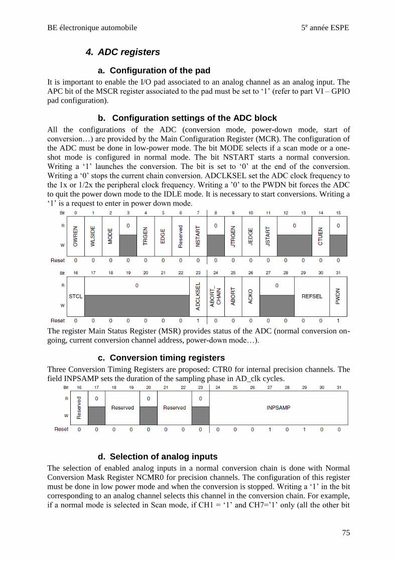
BE électronique automobile 5e année ESPE
75
4. ADC registers
a. Configuration of the pad
It is important to enable the I/O pad associated to an analog channel as an analog input. The
APC bit of the MSCR register associated to the pad must be set to ‘1’ (refer to part VI – GPIO
pad configuration).
b. Configuration settings of the ADC block
All the configurations of the ADC (conversion mode, power-down mode, start of
conversion…) are provided by the Main Configuration Register (MCR). The configuration of
the ADC must be done in low-power mode. The bit MODE selects if a scan mode or a one-
shot mode is configured in normal mode. The bit NSTART starts a normal conversion.
Writing a ‘1’ launches the conversion. The bit is set to ‘0’ at the end of the conversion.
Writing a ‘0’ stops the current chain conversion. ADCLKSEL set the ADC clock frequency to
the 1x or 1/2x the peripheral clock frequency. Writing a ’0’ to the PWDN bit forces the ADC
to quit the power down mode to the IDLE mode. It is necessary to start conversions. Writing a
‘1’ is a request to enter in power down mode.
The register Main Status Register (MSR) provides status of the ADC (normal conversion on-
going, current conversion channel address, power-down mode…).
c. Conversion timing registers
Three Conversion Timing Registers are proposed: CTR0 for internal precision channels. The
field INPSAMP sets the duration of the sampling phase in AD_clk cycles.
d. Selection of analog inputs
The selection of enabled analog inputs in a normal conversion chain is done with Normal
Conversion Mask Register NCMR0 for precision channels. The configuration of this register
must be done in low power mode and when the conversion is stopped. Writing a ‘1’ in the bit
corresponding to an analog channel selects this channel in the conversion chain. For example,
if a normal mode is selected in Scan mode, if CH1 = ‘1’ and CH7=’1’ only (all the other bit

BE électronique automobile 5e année ESPE
76
set to ‘0’), the following conversion sequence will be done continuously: sample/convert
channel 1, sample/convert channel 7, sample/convert channel 1, sample/convert channel 7….
The selection of injected channels is done with the JCMR0 registers.
e. Configuration of interrupts
Several registers are proposed to mask the maskable interrupts associated to the ADC block.
The Interrupt Mask Register (IMR) enables End-of-Conversion type interrupts. The interrupts
are enabled by writing ‘1’ in register bits. The interrupts related to the analog watchdog are
maskable with the register WTIMR.
The register Interrupt Status Register (ISR) gives the interrupt flags associated to the
maskable interrupt enabled by IMR register.
Interrupts can be associated to the end of conversion of each channel with the Channel
Interrupt Mask Registers CIMR0. The register Channel Pending Register CEOCFR0 gives the
interrupt flags associated to the maskable interrupt enabled by CIMR register.
End of conversion interrupts are associated to interrupt vector numbers 496 to 498 for ADC_0
and 500 to 502 for ADC_1 (report to Table 7.16 p 193).
f. Power down configuration
As explained previously, the request of power down entry or exit is set with PWDN bit in
MCR register. It is possible to configure the delay between the exit of power down mode and
the start of the conversion with the Power Down Exit Delay Register (PDEDR).
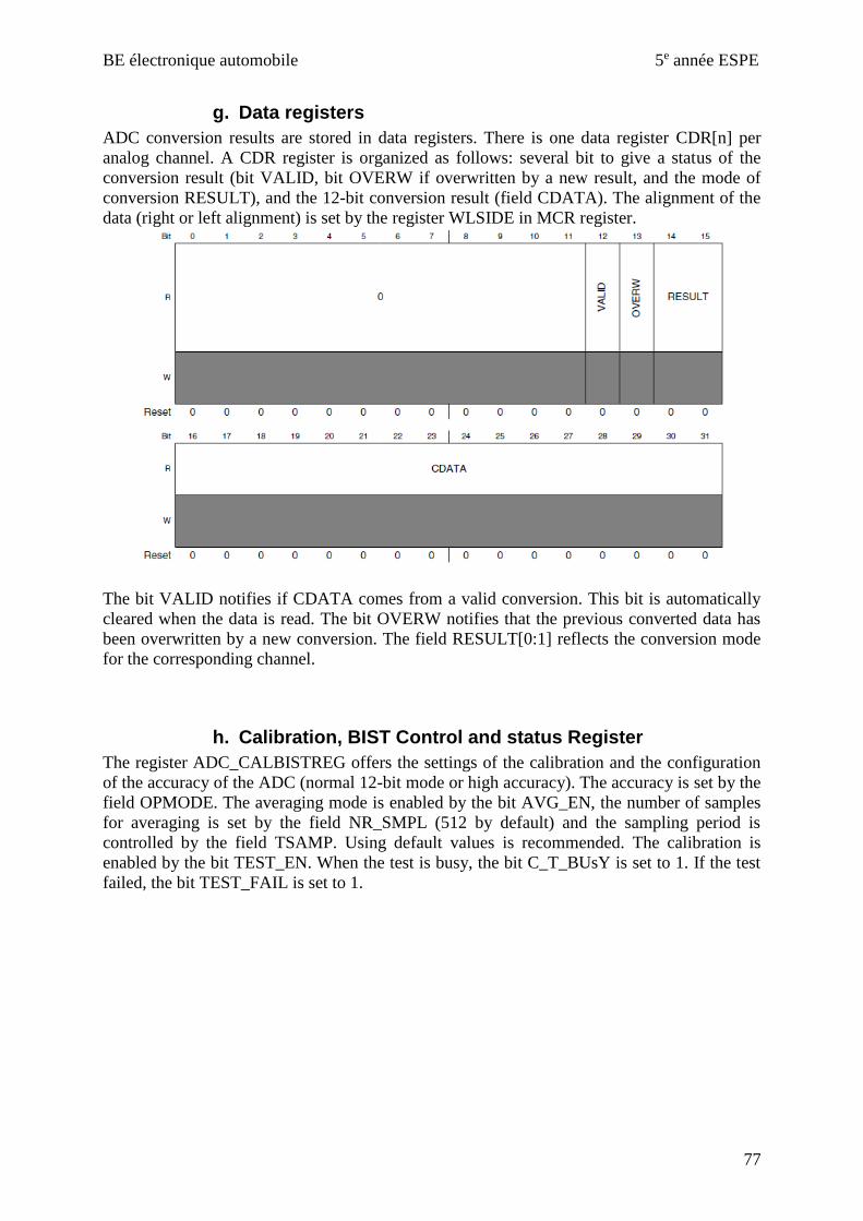
BE électronique automobile 5e année ESPE
77
g. Data registers
ADC conversion results are stored in data registers. There is one data register CDR[n] per
analog channel. A CDR register is organized as follows: several bit to give a status of the
conversion result (bit VALID, bit OVERW if overwritten by a new result, and the mode of
conversion RESULT), and the 12-bit conversion result (field CDATA). The alignment of the
data (right or left alignment) is set by the register WLSIDE in MCR register.
The bit VALID notifies if CDATA comes from a valid conversion. This bit is automatically
cleared when the data is read. The bit OVERW notifies that the previous converted data has
been overwritten by a new conversion. The field RESULT[0:1] reflects the conversion mode
for the corresponding channel.
h. Calibration, BIST Control and status Register
The register ADC_CALBISTREG offers the settings of the calibration and the configuration
of the accuracy of the ADC (normal 12-bit mode or high accuracy). The accuracy is set by the
field OPMODE. The averaging mode is enabled by the bit AVG_EN, the number of samples
for averaging is set by the field NR_SMPL (512 by default) and the sampling period is
controlled by the field TSAMP. Using default values is recommended. The calibration is
enabled by the bit TEST_EN. When the test is busy, the bit C_T_BUsY is set to 1. If the test
failed, the bit TEST_FAIL is set to 1.

BE électronique automobile 5e année ESPE
78
XIV - Periodic interrupt Timer (PIT) Refer to Chapter 44 –Timers for the configuration of periodic interrupt timer (PIT).
The MCU MPC5744P proposes several timer peripherals dedicated to different uses:
▪ System Timer Module (STM): it contains a 32-bit running-up counters clocked by the
MCU system clock and four 32 bit compare channels with individual interrupts. This
block is dedicated to the measurement of code execution time (number of clock
cycles).
▪ Periodic Interrupt Timer (PIT): one PIT module (PIT_0) with four programmable
channels for general purpose time measurements
▪ Software Watchdog Time (SWT): it contains a 32 bit timer used to prevent from
system lock-up when the software is trapped in a loop or a bus transaction failed.
Only PIT will be detailed in this chapter.
The PIT block is an array of 4 programmable timers (or channels) that can trigger maskable
interrupt request each time they reach ‘0’. These timer channels are PIT_0.TIMER[0] to
PIT_0.TIMER[3]. They are associated to 32 bits downcounters.

BE électronique automobile 5e année ESPE
79
The general configuration of PIT block is set by the register MCR. The bit FRZ ensures that
the timers are stopped in debug mode when set. Setting the MDIS bit to ‘0’ enables the clock
for the timers.
The configuration, the count value charging and the interrupt flag are provided by several
registers for each timer channel. The register LDVAL configures the timer start value and
thus the timeout period of the timer (depending on the timer clock period). Writing a value in
this register does not restart the timer. The timer has to be disabled first and then enabled
again. The value is loaded in the timer counter (its current value is indicated by the register
CVAL, only in read mode) at each time-out (i.e. each time it reaches 0). The individual
configuration of each timer channel is set by the register TCTRL. Setting the bit TEN loads
LDVAL value in the timer counter and starts the downcounting operation. Setting the bit TIE
enables interrupt raise each time the timer counter reaches 0.
The bit TIF of the register TFLG is set to 1 when the time-out of the timer channel occurs. If
the interrupt associated to time-out of the channel is enabled, the TIF causes an interrupt
request. To reset the TIF bit, a ’1’ has to be written.
XV - SPI bus and SPI module This chapter aims at providing some elements about hardware architecture and operation
principles of SPI bus, but also the more basic programming elements for the embedded SPI
controller of the MPC5744P. Refer to Chapter 49 –Serial Peripheral Interface for the
configuration of SPI module.
1. Some elements about SPI protocol
The SPI is a synchronous serial communication bus which operates in full-duplex mode. The
communication is based on a master-slave protocol. Several slaves can be placed on the bus,
the selection is done through a Chip Select line.
The bus is made of 4 logical signals:
▪ SCLK: the clock generated by the master
▪ MOSI (Master Output, Slave Input) or Data Out: data sent by the master
▪ MISO (Master Input, Slave Output) or Data In: data sent by the slave

BE électronique automobile 5e année ESPE
80
▪ CS (Chip Select) or PCS (Peripheral Chip Select): selection of the slave by the master,
usually active at low state
The MOSI of the master must be connected to the MISO of the slave and vice-versa. At each
SCLK period, one bit is exchanged. When a data transfer operation is performed, data is
serially shifted by a pre-determined number of bit positions. Because the registers are linked,
data is exchanged between the master and the slave. The data that was in the master’s shift
register is now in the shift register of the slave, and vice versa. The number of bits to
exchange can vary (it must not exceed the size of shift register).
Figure 39 – SPI communication overview
2. Presentation of DSPI module
a. General description
The MCU embeds 4 DSPI modules called SPI_0 to SPI_3 with 4 clock and attribute registers
and 8 Chip Select per module. Each SPI module has the following pins:
▪ CS0: peripheral chip select 0 (slave select in master mode)
▪ CS1 to CS4 and CS6 to CS7: peripheral chip select 1 to 4 and 6 to 7 (unused in slave
mode)
▪ CS4: peripheral chip select 4 (master trigger)
▪ CS5: peripheral chip select 5 (unused in slave mode. In master mode, it is used as a
strobe signal transmitted after CSx signal to prevent from glitches)
▪ SIN: serial data in
▪ SOUT: serial data out
▪ SCK: serial clock
The block diagram of the SPI module is described in Figure 40. The clock bus for SPI
modules is PBRIDGE_clk. This clock source is used to generate the timing parameters of SPI
transfer, through several configurable prescalers.
A 16-bit shift register in master and a 16 bit shift register in slave are associated to SOUT_x,
and SIN_x signals, and form a 32 bit register. The SPI frames can be from 4 to 16 bits long.
The data to be transmitted can come from queues stored in SRAM external to the SPI. Host
software can transfer the SPI data from the queues to a first-in first-out (FIFO) buffer. Host
software can add (or push) entries to the TX FIFO by writing to the SPIx_PUSHR. The SPI
ignores attempts to push data to a full TX FIFO.
The received data is stored in entries in the receive FIFO (RX FIFO) buffer. Host software
transfers the received data from the RX FIFO to memory external to the SPI.

BE électronique automobile 5e année ESPE
81
Figure 40 - Block diagram of SPI module (MPC5744PRM.pdf - Fig. 49-1 - p. 1576)
The SPI has 4 modes of operation:
▪ Master mode (SPI initiates and control the serial communication, the pins SCK, Sout
and CS are outputs and controlled by SPI)
▪ Slave mode (SPI responds to external SPI bus masters and cannot initiate
communications. The SCK and CS pin are configured as input, an internal pull-up
must be configured on CS0_x input. All transfer attributes are controlled by the bus
master, except the clock polarity, clock phase and the number of bits to transfer which
must be configured in the SPI slave to communicate correctly.)
▪ Module disable mode (low power mode)
▪ Debug mode
The SPI has two operating states: STOPPED and RUNNING. The states are independent of
SPI configuration. The default state of the SPI is STOPPED. In the STOPPED state no serial
transfers are initiated in master mode and no transfers are responded to in slave mode. The
STOPPED state is also a safe state for writing the various configuration registers of the SPI
without causing undetermined results. After a reset, the SPI module is in STOPPED state.
b. TX Buffering and transmitting mechanisms
The data field in the executing TX FIFO entry is loaded into the shift register and shifted out
on the serial out (SOUT_x) pin. The TX FIFO functions as a buffer of SPI data and SPI
commands for transmission. SPI commands and data are added to the TX FIFO by writing to
the SPI push TX FIFO register (PUSHR). TX FIFO entries can only be removed from the TX
FIFO by being shifted out or by flushing the TX FIFO. The TX FIFO counter field (TXCTR)
in the SPI status register (SR) indicates the number of valid entries in the TX FIFO. The

BE électronique automobile 5e année ESPE
82
TXCTR is updated every time the DPUSHR is written or SPI data is transferred into the shift
register from the TX FIFO.
The TX FIFO entries are removed (drained) by shifting SPI data out through the shift register.
Entries are transferred from the TX FIFO to the shift register and shifted out as long as there
are valid entries in the TX FIFO. Every time an entry is transferred from the TX FIFO to the
shift register, the TX FIFO counter is decremented by one. At the end of a transfer, the TCF
bit in the SR is set to indicate the completion of a transfer. The TX FIFO is flushed by writing
a ‘1’ to the CLR_TXF bit in MCR. If an external SPI bus master initiates a transfer with a SPI
slave while the slave’s SPI TX FIFO is empty, the transmit FIFO underflow flag (TFUF) in
the slave’s SPIx_SR is set.
Figure 41 – Structure of the TX FIFO and associated counter (MPC5744PRM.pdf - Fig. 49-18 - p. 1630)
c. RX buffering and receiving mechanisms
The RX FIFO functions as a buffer for data received on the SIN pin. The RX FIFO holds four
received SPI data frames. SPI data is added to the RX FIFO at the completion of a transfer
when the received data in the shift register is transferred into the RX FIFO. SPI data is
removed (or popped) from the RX FIFO by reading the SPIx_POPR register. RX FIFO
entries can only be removed from the RX FIFO by reading the SPIx_POPR or by flushing the
RX FIFO. The RX FIFO counter field (RXCTR) in the SPI status register (SPIx_SR)
indicates the number of valid entries in the RX FIFO. The RXCTR is updated every time the
SPI _POPR is read or SPI data is copied from the shift register to the RX FIFO.
The RX FIFO is filled with the received SPI data from the shift register. While the RX FIFO
is not full, SPI frames from the shift register are transferred to the RX FIFO. Every time an
SPI frame is transferred to the RX FIFO, the RX FIFO counter is incremented by one. If the
RX FIFO and shift register are full and a transfer is initiated, the RFOF bit in the SPIx_SR is
set indicating an overflow condition. Depending on the state of the ROOE bit in the
SPIx_MCR, the data from the transfer that generated the overflow is ignored or put in the
shift register. If the ROOE bit is set, the incoming data is put in the shift register. If the ROOE
bit is cleared, the incoming data is ignored.

BE électronique automobile 5e année ESPE
83
Host software can remove (pop) entries from the RX FIFO by reading the SPIx_POPR. A
read of the SPIx_POPR decrements the RX FIFO counter by one. Attempts to pop data from
an empty RX FIFO are ignored, the RX FIFO counter remains unchanged. The data returned
from reading an empty RX FIFO is undetermined.
d. Transfer attributes
The transfer attributes define the baud rate, the clock polarity, the delays between clock edge
and CS and data sampling… In master mode, they define SCK signal properties. In Slave
mode, the transfer attributes of SPI must be the same than the Master transfer attribute to
ensure a correct reception.
The SPI module contains 4 CTAR register which defines the transfer attributes. The SPI slave
mode transfer attributes are set in the CTAR0_SLAVE.
When the SPI is the bus master, the CPOL and CPHA bits in the CTAR registers select the
polarity and phase of the serial clock, SCK_x. The polarity bit selects the idle state of the
SCK_x. The clock phase bit selects if the data on SOUT_x is valid before or on the first
SCK_x edge. In slave mode, clock polarity, clock phase and number of bits to transfer must
be identical for the master device and the slave device to ensure proper transmission.
The frame size is configurable from 4 to 16 with the field FMSZ.
The SCK_x frequency and the delay values for serial transfer are generated by dividing the
system clock frequency by a prescaler and a scaler with the option of doubling the baud rate.
The baud rate is the frequency of the serial communication clock (SCK_x). The system clock
is divided by a baud rate prescaler (defined by CTAR[PBR]) and baud rate scaler (defined by
CTAR[BR]) to produce SCK_x with the possibility of doubling the baud rate. The DBR, PBR,
and BR fields in the CTARs select the frequency of SCK_x using the following formula:
The CS_x to SCK_x delay is the length of time from assertion of the CS_x signal to the first
SCK_x edge.
The after SCK_x delay is the length of time between the last edge of SCK_x and the negation
of CS_x.
The delay after transfer is the length of time between negation of the CSx signal for a frame
and the assertion of the CSx signal for the next frame.
e. Interrupts
The SPI has five conditions that can generate interrupt requests:
▪ End of transfer queue has been reached (flag EOQF): it indicates that the end of a
transmit queue is reached. The end of queue request is generated when the EOQ bit in
the executing SPI command is asserted and the EOQF_RE bit in the RSER is set.

BE électronique automobile 5e année ESPE
84
▪ Current frame transfer is complete (flag TCF): it indicates the end of the transfer of a
serial frame. The transfer complete request is generated at the end of each frame
transfer when the TCF_RE bit is set in the RSER.
▪ TX FIFO underflow has occurred (flag TFUF): it indicates that an underflow
condition in the TX FIFO has occurred. If an external SPI bus master initiates a
transfer with a SPI slave while the slave’s TX FIFO is empty, the transmit FIFO
underflow flag (TFUF) in the slave’s SR is set. If the TFUF bit is set while the
TFUF_RE bit in the RSER is set, an interrupt request is generated.
▪ RX FIFO overflow has occurred (flag RFOF): it indicates that an overflow condition
in the RX FIFO has occurred. A receive FIFO overflow request is generated when RX
FIFO and shift register are full and a transfer is initiated. The RFOF_RE bit in the
RSER must be set for the interrupt request to be generated. Depending on the state of
the ROOE bit in the MCR, the data from the transfer that generated the overflow is
either ignored or shifted in to the shift register. If the ROOE bit is set, the incoming
data is shifted in to the shift register. If the ROOE bit is negated, the incoming data is
ignored.
▪ FIFO overrun has occurred (flag TFUF or RFOF): it indicates that at least one of the
FIFOs in the SPI has exceeded its capacity. The FIFO overrun request is generated by
logically OR’ing together the RX FIFO overflow and TX FIFO underflow signals.
3. Configuration of the SPI module
a. Module configuration
The module configuration is ensured by the MCR register.
The bit MSTR configures the module in Master (‘1’) or Slave (‘0’) mode. The MDIS bit
allows the module disable mode entry. The FRZ bit stops SPI transfer when the device enters
in debug mode. The bit HALT provides a mechanism for software to start (‘0’) and stop (‘1’)

BE électronique automobile 5e année ESPE
85
DSPI transfer: transition from STOPPED to RUNNING mode. The bits DIS_TXF and
DIS_RXF disable RX and TX FIFO. The bits CLR_TXF and CLR_RXF clear or flush the TX
or RX FIFO by clearing the associated counter. See MCU datasheet for details about the other
bits.
The bits in PCSIS enables/disables the corresponding eight peripheral chip select signals.
b. Clock and transfer attributes
The SPI modules contain four clock and transfer attribute registers (CTAR[n]) which are used
to define different transfer attribute configurations. Each CTAR controls the frame size, the
Baud rate and transfer delay values, the clock phase and polarity and defines if MSB or LSB
is considered as first bit. Do not write in this register in RUNNING mode (HALT = 0).
In slave mode, CTAR0_SLAVE is used to set the slave transfer attributes. When the SPI is
configured as an SPI master, the CTAS field in the command portion of the TX FIFO entry
selects which of the SPIx_CTAR registers is used on a per-frame basis.
The field FMSZ defines the frame size (from 4 to 16). The number of bits transferred per
frame is equal to the FMSZ value plus 1. CPOL bit defines the clock polarity, i.e. the inactive
state of SCLK. CPHA defines the clock phase, i.e. which SCK edge causes the data to change
or to be captured. The bit LSBFE defines if the LSB or MSB is transferred first.
The baud rate depends on DBR, PBR and BR bit fields (see datasheet for more information
about computation of bit rate). Depending on DBR, PBR and CPHA, duty cycle of SCLK is
changed.
The fields PCSSCK, PASC, PDT, CSSCK, ASC and DT define different delays between
either SCK, CS and data.
c. TX FIFO writing
Data are written by software in TX FIFO by the Push TX FIFO register PUSHR. Data written
in this register are written in TX FIFO. This register contains command bits and data (16 bits).
The field CTAS defines which CTAR register is used for clock and transfer attributes. The bit
PCSx defines if signal CSx is asserted during transfer. Setting CONT to '1' asserts the CS
signal to '0' between transfers. As normal frame size is 8 or 16 bits for this MCU, this option
can be useful for transfer with frame size larger 16 bits. When the module is disabled, writing
to this register does not update the FIFO. Therefore, any reads performed while the module is
disabled return the last PUSHR write performed while the module was still enabled.

BE électronique automobile 5e année ESPE
86
The data in TX FIFO are visible in registers TXFRn (n from 0 to 3). They are read-only
registers and cannot be modified.
Tips: An 8- or 16-bit write access transfers all 32 bits to the TX FIFO. Thus, update all the
fields of this register simultaneously !
d. RX FIFO writing
Received data can be read by software in RX FIFO through the POP RX register POPR. This
register contains only received data (16 bits). Once the RX FIFO is read, the read data pointer
is moved to the next entry in the RX FIFO. Therefore, read POPR only when you need the
data. A write to this register will generate a Transfer Error.
The data in RX FIFO are visible in registers RXFRn (n from 0 to 3). They are read-only
registers and cannot be modified.
Tips: the POPR register is cleared after a reading. However, it can generate application error
during in-situ debugging. Indeed, each time the debugging tool reads POPR, this register will
be cleared. For example, if the application software embedded in MCU memory reads POPR
just after the debugging tool, POPR has been cleared to the reading of POPR by the
application software will return 0 instead of the actual value received by SPI. During
debugging session, it is recommended to not read POPR to prevent this problem.
e. Interrupt/DMA configuration and status
The RSER enables flag bits in the SR to generate interrupt requests. Do not write to the RSER
while the SPI is running.

BE électronique automobile 5e année ESPE
87
The status of the module is indicated by flag bits in status register SR. They are set by
hardware and reflect the status of SPI module. They can be cleared by software only by
writing ‘1’.
TCF flag indicates that a transfer is completed, i.e. all bits in a frame have been shifted out.
EOQF flag indicates that the last entry in queue transmission is ongoing. The flag TFFF
indicates that the TX FIFO is not full and be filled. It is cleared by software or when the FIFO
is full.
RFDF flag indicates the the RX FIFO is not empty and the received data can be drained in
POPR register. The flags TFUF and RFOF reflect TX FIFO underflow and RX FIFO
overflow conditions.
The bit TXRXS indicates that TX and RX operation are enabled (RUNNING state) or
disabled (STOPPED mode). TXCTR and RXCTR are TX and RX FIFO counter.
TXNXTPTR indicates which entry in TX FIFO will be transmitted during the next transfer.
POPNXTPTR contains a pointer to the RX FIFO entry that is returned when the POPR is read.
The POPNXTPTR is updated when the POPR is read.
XVI - UART with LINFlex module The main purpose of LINFlex module is the management of LIN communication, which is a
robust low-data rate bus widely-used in automotive. However, LINFlex also provides support

BE électronique automobile 5e année ESPE
88
for UART transfers. Data can be read by an hyperterminal for debugging purpose. Another
possible use for debugging motor control applications is the interfacing with Freemaster tool.
This chapter aims at describing how to configure LINFlex as UART interface. More
information about LINFlex can be found in Chapter 52 - LINFlexD of the reference manual.
1. Presentation of the LINFlex module in UART mode
MPC5744P contains two LINFlex modules: LINFlex0 and LINFlex2, with UART and LIN
with DMA support. The module uses two different clocks: HALF_SYSCLK to generate the
baud rate of the signal, and PBRIDGE_clk for all the other functions. Full-duplex
8/9/13/16/17-bit communication is supported. A parity bit can be added to each frame. The
structure of the frame is illustrated in Figure 42 for a 8-bit data frame.
Figure 42 – Structure of the 8-bit data frame in UART mode (MPC5744PRM.pdf - Fig. 52-15 - p. 1965)
Transmitted or received messages are stored in a 8 bytes buffer, whose structure is described
in Figure 43. This buffer is divided in two parts: the first four bytes are dedicated for
transmission (Tx0 to Tx3, i.e. BDR0 to BDR3), while the last four are for reception (Rx0 to
Rx3, i.e. BDR4 to BDR7). In case of 16-bit frame, the lower significant eight bits are written
in BDR0 and the upper significant eight bits in BDR1. It is the same for reception.
Figure 43 – Structure of the 8-bytes UART mode (MPC5744PRM.pdf - Fig. 52-20 - p. 1967)
2. Configuration
a. Initialization of LINFlex module
The configuration of the module can be done only in initialization mode. LINCR1 register
consists of control bits used to configure features of the LINFlexD. The bit SLEEP is set to '1'
to enter in Sleep mode. The bit INIT is set to '1' to enter in initialization mode. After clearing
INIT and SLEEP, the module enters in normal mode, either if it is used in LIN or UART
mode. Once all the initialization is finished, the module must exit the initialization mode by
setting INIT to '0'.

BE électronique automobile 5e année ESPE
89
b. Configuration for UART mode
The configuration of the UART mode depends on the register UARTCR. The bit UART has
to be set to '1' to enable UART mode and start the configuration of this mode. TxEN and
RxEN enables the transmitter and the receiver respectively.
WL0 and WL1 sets the word length in UART mode (if WLS is set, special word length is
used). PCE enables the presence of parity bit. The parity control is configured by the bits PC0
and PC1. The number of stop bits is set by SBUR bits.
Transmitter and receiver are configured in buffer or FIFO mode according to bits TFBM and
RFBM. The fields TFDL_TFC and TFDL_RFC define the number of bytes to be transmitted
or received when the module is configured in buffer mode.
c. Status of the UART
The register UARTSR gives the status of the LINFlex module in UART mode. The bit
DTFTFF is set by hardware (if in buffer mode) to indicate that data transmission is completed.
The bit DRFRFE indicates that the number of bytes programmed in RDFL have been received.
The bit RMB indicates that the data in the reception buffer can be read.
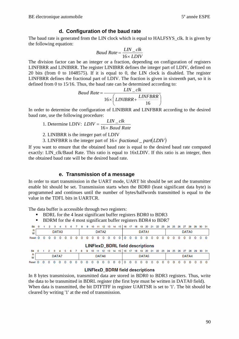
BE électronique automobile 5e année ESPE
90
d. Configuration of the baud rate
The baud rate is generated from the LIN clock which is equal to HALFSYS_clk. It is given by
the following equation:
LDIV
clkLINRateBaud
=
16
_
The division factor can be an integer or a fraction, depending on configuration of registers
LINFBRR and LINIBRR. The register LINIBRR defines the integer part of LDIV, defined on
20 bits (from 0 to 1048575). If it is equal to 0, the LIN clock is disabled. The register
LINFBRR defines the fractional part of LDIV. The fraction is given in sixteenth part, so it is
defined from 0 to 15/16. Thus, the baud rate can be determined according to:
+
=
1616
_
LINFBRRLINIBRR
clkLINRateBaud
In order to determine the configuration of LINIBRR and LINFBRR according to the desired
baud rate, use the following procedure:
1. Determine LDIV: RateBaud
clkLINLDIV
=
16
_
2. LINIBRR is the integer part of LDIV
3. LINFBRR is the integer part of ( )LDIVpartfractional _16
If you want to ensure that the obtained baud rate is equal to the desired baud rate computed
exactly: LIN_clk/Baud Rate. This ratio is equal to 16xLDIV. If this ratio is an integer, then
the obtained baud rate will be the desired baud rate.
e. Transmission of a message
In order to start transmission in the UART mode, UART bit should be set and the transmitter
enable bit should be set. Transmission starts when the BDR0 (least significant data byte) is
programmed and continues until the number of bytes/halfwords transmitted is equal to the
value in the TDFL bits in UARTCR.
The data buffer is accessible through two registers:
▪ BDRL for the 4 least significant buffer registers BDR0 to BDR3
▪ BDRM for the 4 most significant buffer registers BDR4 to BDR7
In 8 bytes transmission, transmitted data are stored in BDR0 to BDR3 registers. Thus, write
the data to be transmitted in BDRL register (the first byte must be written in DATA0 field).
When data is transmitted, the bit DTFTFF in register UARTSR is set to '1'. The bit should be
cleared by writing '1' at the end of transmission.

BE électronique automobile 5e année ESPE
91
f. Reception of a message
The reception of a message is indicated by the flag DRFRFE in UARTSR register. A message
consists in a number of bytes defined by the field RDLF_RFC in UARTCR register. When
the buffer data are ready to be read, the bit RMB in UARTSR is set to '1'.
In 8 bytes reception, received data are stored in BDR4 to BDR7 registers. The data can be
read in BDRM register. After the reception of the message, clear the bits DRFRFE and RMB
by writing '1'.
XVII - Fault Collection and Control Unit (FCCU) FCCU is one of the central block in safety management of MPC5744P. This chapter aims at
describing how to configure the FCCU. More information about FCCU can be found in
Chapter 69 of the reference manual.
1. Presentation - Overview
The Fault Collection and Control Unit (FCCU) offers a hardware peripheral which aims at
collecting faults and placing the MCU into a safe state when a failure in the device is
detected, without any CPU intervention.
FCCU has the following main features:
▪ Configurable fault control (from HW or SW faults)
▪ Configurable internal reactions for each non-critical fault (NCF): no reaction, IRQ
(alarm state), short/long functional reset and non-maskable interrupt (NMI) (fault state)
▪ External reactions via two configurable output pins
▪ Lockable configuration
▪ Fault injection (for test purpose)
▪ Lockable configuration
The block diagram of the FCCU is shown below:
▪ the REG interface includes the register file, the IPS bus interface, the IRQ interface
and the parity block (PB) for the configuration registers
▪ the HNSHK blocks (master and slave) includes the FSM's ability to support the
handshake between the REG interface and the FSM unit due to the usage of 2
asynchronous clocks (IPS system clock and RC oscillator clock)
▪ the Finite State Machine (FSM) unit implements the main functions of the FCCU
▪ the FAULT interface is dedicated to fault conditioning and management
▪ EOUT0 and EOUT1 interfaces manage EOUT[1:0] error outputs
The FCCU is clocked by CLKSYS primarily, but also by CLKSAFE 0 and 1 provided by a
RC oscillator which produces two redundant 16 MHz clocks. CLKSAFE0 and 1 are often
referred to as the same clock (CLKSAFE). CLKSAFE is not synchronized on CLKSYS.
FCCU is designed to function when CLKSYS is faster than the CLKSAFE clocks.
FCCU is connected to Reset Generation Module (RGM) and interrupt controller (INTC).
Depending on the type of faults and FCCU configuration, an IRQ or MCU reset can be
generated on fault detection. The FCCU is also connected to the wake up unit module to force
the MCU to exit a sleep mode in case of fault, and to the CPU to send it non maskable
interrupts (NMI) request when the FCCU enters in a Fault state.

BE électronique automobile 5e année ESPE
92
Figure 44 – FCCU block diagram (MPC5744PRM.pdf - Fig. 69-1 - p. 2720)
The FCCU provides two bidirectional signals (EOUT[1:0]) as a failure indication to the
external world. Different fault-output modes (protocols) for the fault-output (EOUT) interface
are supported (FCCU_CFG[FOM]): dual rail encoding, time-switching protocol, bistable
protocol.
The FCCU collects faults from 75 sources, whicn may trigger Non-Critical Fault (NCF)
depending on FCCU configuration by the user. The mapping between the NCF and the fault
sources is given in Table 7-33 p 236 of the MPC5744P reference manual.
The FCCU manages fault recovery according to two methods:
▪ HW recovery fault: the fault signal is latched externally to the FCCU in the module
where the fault occurred. The fault indication is an edge-triggered and level-sensitive
signal that remains asserted until the fault cause is deasserted. The status is
automatically cleared when the fault signal goes to 1. No SW intervention in the
FCCU is required to recover the fault condition.
▪ SW recoverable fault: The fault signal is latched in the FCCU. The fault recovery is
executed following a SW recovery procedure (status/flag register clearing).
FCCU supports three types of reset:
▪ destructive: the entire chip is initialized as a result of a power-failure condition
▪ long functional: the digital circuitry is initialized except the FCCU and STCU2 (Self-
Test Control Unit, dedicated to the built-in-self test)
▪ short functional: the digital circuitry is initialized except the FCCU, OCOTP and
STCU2
2. Functional description of FCCU
The operation of the FCCU is described by a finite state machine shown in Figure 45, where
four states can be identified:
▪ CONFIG: this mode is used to change the configuration of FCCU, through a subset of
configuration registers accessible only in write mode. This mode is accessible from the
NORMAL mode and only if the configuration has not been locked. The Configuration
to Normal state transition can be executed by SW or automatically following a timeout

BE électronique automobile 5e année ESPE
93
condition of the watchdog. The incoming faults, occurring during the configuration
phase will be processed during the NORMAL state.
▪ NORMAL: this is the operating state when no faults occur or after a reset exit.
Transitions occur when:
o unmasked noncritical faults with the timeout disabled → FCCU moves to Fault
state
o unmasked noncritical faults with the timeout enabled → FCCU moves to
Alarm state
o masked noncritical faults → FCCU stays in Normal state
▪ ALARM: FCCU moves into this state when an unmasked noncritical fault occurs and
the timeout is enabled. this fault may be recovered within a programmable timeout
period, before it generates a transition to Fault state. The timeout is reinitialized if
FCCU enters Normal state.
▪ FAULT: FCCU moves into this state either when timeout related to a noncritical fault
when FCCU is in Alarm state, or when unmasked noncritical faults with the timeout
disabled
The transition between NORMAL, ALARM and FAULT states may trigger NMI interrupt,
EOUT signaling, short/long functional reset. Multiple faults can occur at the same time. If
only one fault is configured without alarm, the FCCU will enter directly in FAULT state. This
is due to the priority scheme given to fault and alarm: Fault has a higher priority than Alarm.
The FAULT to NORMAL state transition occurs only if all the NCF have been cleared.
Figure 45 – FCCU state diagram (MPC5744PRM.pdf - Fig. 69-2 - p. 2725)
3. EOUT interface
EOUT[1:0] error pads provide two bidirectional signals provided by FCCU to indicate MCU
failure to external components (e.g. power system basis chip). These output signals support
different protocols:
▪ Dual-rail: in non-faulty condition or CONFIG mode, EOUT[1] and EOUT[0] toggle
and have inverted logical state (toggling between '01' and '10'). In case of fault, they
continue to toggle but they have the same logical state ('00' and '11'). In RESET mode,

BE électronique automobile 5e année ESPE
94
they are in high impedance state so they do not toggle. The toggling frequency is 61
Hz.
▪ Time-switching: in NORMAL or ALARM state, EOUT[1] and EOUT[0] toggle at a
frequency defined by CFG[FOP] and have inverted logical state. The frequency of this
signal is derived from CLKSAFE. In FAULT state, EOUT[0] is set to '0' and EOUT[1]
to '1'. In RESET mode, they are in high impedance state so they do not toggle.
▪ Bistable: EOUT[1:0] do not toggle in this protocol. In non faulty condition or
CONFIG mode, EOUT[1:0] = '01'. In faulty condition, EOUT[1:0] = '10'. In RESET
mode, they are in high impedance state.
In dual-rail and time-switching protocols, two switching modes can be defined according to
the bit SM in CFG register. In slow switching mode, NORMAL - FAULT transition is
indicated after a maximum delay equal to the half-period of the toggling period. Thus, there is
no timing violation of EOUT signaling protocol. In fast switching mode, NORMAL - FAULT
transition is indicated immediately.
4. FCCU Output Supervision Unit (FOSU)
The FOSU block ensures a supervision of the correctness of the FCCU response. If the FCCU
fails to respond in a given time window after a fault is signaled (given by the timer
FOSU_COUNT), a destructive reset is triggered. If the FCCU has a reaction to the incoming
fault (IRQ, Error out, reset), the FOSU timer stops. The value of FOSU_COUNT is 65535
IRCOSC clock cycles, i.e. 4.096 ms.
An important thing to note is that the FCCU cannot have any reaction to incoming faults
during CONFIG state. If a fault triggers during CONFIG and if the FCCU remains in this
state for a too long time, FOSU will reset the circuit. That's why the FCCU should not be kept
in CONFIG for longer than the FOSU_COUNT duration.
5. FCCU configuration
The FCCU contains numerous configuration registers to define the reaction of the FCCU to
incoming faults. All these registers are accessible in write mode only in CONFIG states.
These configuration registers return to the default value after configuration watchdog timer
expires. So the time to configure FCCU registers is limited. These registers can also be locked
by FCCU_TRANS_LOCK and FCCU_PERMNT_LOCK registers. The configuration register
setting has effect only when the FCCU state exits from the CONFIG state.
For each possible NCF failure source a different reaction shall be configurable through the
use of NMI, IRQ, long/short reset selection registers as well as no reaction by disabling the
former registers. It is not possible for a single event upset to switch off all reactions on
failures as implementation is per fault source (but it will be possible to switch them all off by
SW if intended). Failures themselves are not able to disable all reactions and indications.
a. Configuration entry/exit
A specific procedure has to be followed to enter in CONFIG mode or exit this mode:
▪ 1. Write the key into the CTRLK register
▪ 2. Write the CTRL register (operations OP1 or OP2 )

BE électronique automobile 5e année ESPE
95
OP1 means 'Set the FCCU into the CONFIG state' and OP2 ' Set the FCCU into the
NORMAL state'. The key to write into CTRLK for OP1 is 0x913756AF, and is 0x825A132B
for OP2.
Then, write in the field OPR of register CTRL the code of the operation (enter CONFIG or
NORMAL mode): '0001' for OP1 and '0010' for OP2.
b. Global configuration of FCCU
The global configuration of FCCU is defined by the register CFG. It consists mainly in the
configuration of EOUT[1:0] pins. If FCCU_SET_AFTER_RESET is set to '1', the FCCU
starts functioning after a power-on reset. FCCU_SET_CLEAR defines the error pin state
during FAULT. The toggling frequency of error output signal is defined by bit FOPE and
field FOP according to the following equation:
The EOUT polarity during FAULT is defined by bit PS (only in time switching and Bistable
protocols). The error signaling protocol is selected by bits FOM.
c. Configuration of fault-recovery management for NCF
This ensured by the registers NCF_CFG[0..2] registers Each configuration register is
associated to 32 NCF channels.
Each bit of these registers define the fault recovery mode:

BE électronique automobile 5e année ESPE
96
▪ if 0, a hardware-recovery fault mechanism is selected. They are self-recovered if the
root cause has been removed. In other word, if the input fault disappears, the related
status flag is cleared.
▪ if 1, software-recovery fault mechanism is selected. They are recovered by software,
i.e. when the software clears the associated status flag.
Hardware recoverable faults should be configured only if a previous latching stage captures
and holds the physical fault; otherwise, the fault can be lost. All other faults should be
configured as software faults.
The fault reaction is defined by the NCFS_CFG[0..4] registers (short or long functional reset
request pulse). Each configuration register is associated to 16 NCF channels.
Four reactions can be defined, according to the NCFSCx bits:
The NCF_S[0..2] registers contain the latched fault indication collected from the NCF sources.
Faults are latched also in the CONFIG state. No reactions are executed until the FCCU moves
in the NORMAL state.
FCCU reacts and moves from the NORMAL state into the ALARM state only if the
respective enable bit for a fault is set in the NCF_Ex register and the respective enable bit for
the timeout is set in the TOEx register. FCCU reacts and moves from the NORMAL or
ALARM state into the FAULT state if the respective enable bit for a fault is set in the
NCF_Ex register and the respective enable bit for the timeout is disabled in the TOEx register.
FCCU reacts and moves from the ALARM state into the FAULT state if the timeout (TO
register) is elapsed before recovering from the fault. The timeout is stopped only when the
FCCU returns in the NORMAL state.
The FCCU moves from the FAULT or ALARM state into the NORMAL state if all the
source faults that caused the transition into the FAULT state have been removed (HW
recoverable fault) or cleared via SW (SW recoverable fault).
The status bits of the NCF_Sx register, configured as SW recoverable faults, can be cleared
by the following locked sequence:
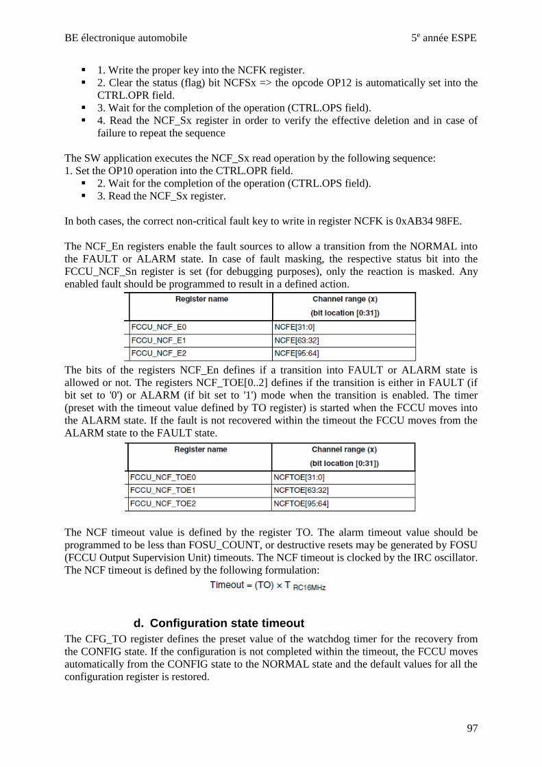
BE électronique automobile 5e année ESPE
97
▪ 1. Write the proper key into the NCFK register.
▪ 2. Clear the status (flag) bit NCFSx => the opcode OP12 is automatically set into the
CTRL.OPR field.
▪ 3. Wait for the completion of the operation (CTRL.OPS field).
▪ 4. Read the NCF_Sx register in order to verify the effective deletion and in case of
failure to repeat the sequence
The SW application executes the NCF_Sx read operation by the following sequence:
1. Set the OP10 operation into the CTRL.OPR field.
▪ 2. Wait for the completion of the operation (CTRL.OPS field).
▪ 3. Read the NCF_Sx register.
In both cases, the correct non-critical fault key to write in register NCFK is 0xAB34 98FE.
The NCF_En registers enable the fault sources to allow a transition from the NORMAL into
the FAULT or ALARM state. In case of fault masking, the respective status bit into the
FCCU_NCF_Sn register is set (for debugging purposes), only the reaction is masked. Any
enabled fault should be programmed to result in a defined action.
The bits of the registers NCF_En defines if a transition into FAULT or ALARM state is
allowed or not. The registers NCF_TOE[0..2] defines if the transition is either in FAULT (if
bit set to '0') or ALARM (if bit set to '1') mode when the transition is enabled. The timer
(preset with the timeout value defined by TO register) is started when the FCCU moves into
the ALARM state. If the fault is not recovered within the timeout the FCCU moves from the
ALARM state to the FAULT state.
The NCF timeout value is defined by the register TO. The alarm timeout value should be
programmed to be less than FOSU_COUNT, or destructive resets may be generated by FOSU
(FCCU Output Supervision Unit) timeouts. The NCF timeout is clocked by the IRC oscillator.
The NCF timeout is defined by the following formulation:
d. Configuration state timeout
The CFG_TO register defines the preset value of the watchdog timer for the recovery from
the CONFIG state. If the configuration is not completed within the timeout, the FCCU moves
automatically from the CONFIG state to the NORMAL state and the default values for all the
configuration register is restored.

BE électronique automobile 5e année ESPE
98
The watchdog timeout is clocked by CLKSAFE. The default timeout value is 4.096 ms.
Longer activation of CONFIG state can lead to resets if a failure is indicated during the time
the FCCU is in CONFIG state due to FOSU. The configuration timeout is defined according
to the following formulation.
Both Alarm and configuration timeout are related to watchdogs, whose counter values can be
read in register XTMR. The content of this register can be read according to a specific
procedure.
e. Status of the FCCU - source identification
The FCCU status is provided by the register STAT: if the system is in fault state, the status of
the error pins and the FCCU. The SW application executes a FCCU status read operation by
the following sequence:
▪ 1. Set the OP3 operation into the CTRL.OPR field.
▪ 2. Wait for the completion of the operation (CTRL.OPS field).
▪ 3. Read the FCCU status (STAT register).
The source of the NCF can be identified by the register N2AF status. A specific code is given
to each NCF source. However, in case of multiple NCF, the source cannot be identified. A
specific procedure has to be followed to read it:
▪ 1. Set the OP4 operation into the CTRL.OPR field.
▪ 2. Wait for the completion of the operation (CTRL.OPS field).
▪ 3. Read the N2AF_STATUS register.
The bit status can be cleared according to the following procedure:
▪ 1. Set the OP13 operation into the CTRL.OPR field.
▪ 2. Wait for the completion of the operation (CTRL.OPS field). (All the freeze registers
are cleared by this operation.)
Similarly, A2FF_STATUS register is used to identify the timeout trigger that caused the state
transition from the ALARM state to the FAULT state. A2FF can be read according to the
following procedure:
▪ 1. Set the OP5 operation into the CTRL.OPR field.
▪ 2. Wait for the completion of the operation (FCCU_CTRL.OPS field).
▪ 3. Read the A2FF_STATUS register.
It can be cleared according to:
▪ 1. Set the OP13 operation into the CTRL.OPR field.
▪ 2. Wait for the completion of the operation (CTRL.OPS field).
Similarly, N2FF_STATUS register can be used to identify the source of the NCF that caused
the state transition from the NORMAL state to the FAULT state. To read this register:
▪ 1. Set the OP6 operation into the CTRL.OPR field.
▪ 2. Wait for the completion of the operation (CTRL.OPS field).
▪ 3. Read the N2FF_STATUS register.
To clear it:
▪ 1. Set the OP13 operation into the CTRL.OPR field.

BE électronique automobile 5e année ESPE
99
▪ 2. Wait for the completion of the operation (CTRL.OPS field).
Similarly, F2A_STATUS register can be used to identify the source of the NCF that caused
the state transition from the FAULT state to the ALARM state. To read this register:
▪ 1. Set the OP7 operation into the CTRL.OPR field.
▪ 2. Wait for the completion of the operation (CTRL.OPS field).
▪ 3. Read the N2FF_STATUS register.
To clear it:
▪ 1. Set the OP13 operation into the CTRL.OPR field.
▪ 2. Wait for the completion of the operation (CTRL.OPS field).
f. Software emulation of NCF
The register NCFF is used to generate fake faults. It is useful to verify the correct reaction of
the FCCU in case of NCF triggering.
g. Interrupt requests
Interrupt requests from the FCCU are enabled by the register IRQ_EN. Only the configuration
timeout error is considered. The bit CFG_TO_IEN must be set and also the bit
CFG_TO_STAT of the register IRQ_STAT.
IRQ_STAT register provides the FCCU interrupt status related to the following events:
▪ Configuration timeout error
▪ Alarm interrupt
▪ NMI interrupt
The registers IRQ_ALARM_EN[x] provides bits to enable the IRQ when an alarm is
triggered, according to the NCF channel source.
Non-maskable interrupts are generated according to the configuration of register NMI_EN[x].
h. Fault-output signaling
Registers EOUT_SIG_EN[x] to enable fault outputs depending on the NCF channel.

BE électronique automobile 5e année ESPE
100
Fault-output (EOUT) signaling is enabled for the associated noncritical fault channels when
FCCU is configured for Bistable fault-output mode


![Untitled-2 [] · Romance Pink Avadable in Ramco PRODUCTS . An Clin Angelina Available in 5 ml ... PANTHER PANTHER PANTHER PANTHER Black Panther Available in 100 Ramco](https://img.dokumen.tips/doc/110x75/5b5319867f8b9a0d398b631e/untitled-2-romance-pink-avadable-in-ramco-products-an-clin-angelina-available.jpg)