Embed Size (px)
Citation preview
PREPARATION AND CHARACTERIZATIONOF POLYMER COMPOSITES CONTAINING
GOLD NANOPARTICLES
a dissertation submitted to
the department of chemistry
and the graduate school of engineering and science
of bilkent university
in partial fulfillment of the requirements
for the degree of
doctor of philosophy
By
Eda Yılmaz
September, 2011
I certify that I have read this thesis and that in my opinion it is fully adequate,
in scope and in quality, as a dissertation for the degree of doctor of philosophy.
Prof. Dr. Sefik Suzer (Advisor)
I certify that I have read this thesis and that in my opinion it is fully adequate,
in scope and in quality, as a dissertation for the degree of doctor of philosophy.
Prof. Dr. Erdal Bayramlı
I certify that I have read this thesis and that in my opinion it is fully adequate,
in scope and in quality, as a dissertation for the degree of doctor of philosophy.
Assoc. Prof. Dr. Margarita Kantcheva
ii
I certify that I have read this thesis and that in my opinion it is fully adequate,
in scope and in quality, as a dissertation for the degree of doctor of philosophy.
Assist. Prof. Dr. Erman Bengu
I certify that I have read this thesis and that in my opinion it is fully adequate,
in scope and in quality, as a dissertation for the degree of doctor of philosophy.
Assist. Prof. Dr. Coskun Kocabas
Approved for the Institute of Engineering and Science:
Prof. Dr. Levent OnuralDirector of the Institute
iii
IV
ABSTRACT
PREPARATION AND CHARACTERIZATION OF POLYMER COMPOSITES
CONTAINING GOLD NANOPARTICLES
EDA YILMAZ
Ph.D. in Chemistry
Supervisor: Prof. Dr. Şefik Süzer
September, 2011
In this study, light-assisted synthesis of gold nanoparticles in polymer films is demonstrated
and characterization of gold nanoparticle-polymer composites using various techniques is
shown. There are various methods introduced for the synthesis of gold nanoparticles in
solution and their integration to the polymer films afterwards. However, synthesizing gold
nanoparticles directly inside the polymer matrix is more advantageous for the production of
polymer-nanoparticle composites.
An advantage of synthesizing gold nanoparticles within polymer films is the opportunity of
photo-patterning. Films having patterns made of regions with and without gold nanoparticles
can be produced, using masks designed to cut off the radiation at desired places. Such
patterned films were investigated with scanning electron microscope (SEM) and dark regions
between irradiated regions and masked regions were observed. These dark regions are shown
to be “ion depleted regions”, where gold ions diffuse through irradiated regions during the
irradiation. These regions of about 10 m width, suggests a very large distance for gold ions
to diffuse through a rigid matrix like Poly(methyl methacrylate)(PMMA), which is very
interesting. Supporting evidence for the existence of these regions was obtained from
fluorescence studies with Rhodamine 6G molecule and x-ray electron spectroscopy (XPS).
The observations made through the formation of ion depleted regions can be used to estimate
the diffusion constant of gold ions inside the PMMA matrix. Also the presence of ion
depleted regions indicate the stability of photo-patterns created on the polymer film against
V
smearing during light exposure after the production, by setting an upper limit to the critical
feature size.
During the characterization of gold nanoparticle-polymer composites, the electrical properties
of PMMA with and without gold nanoparticles were investigated using charge resolved XPS,
while applying external bias to the films with and without gold nanoparticles to probe the
charging properties of the films. An enhancement of conductivity of PMMA films containing
gold nanoparticles was observed using this technique. Additionally charge resolved XPS
technique was also used to determine the charge storage characteristics of the polymer
surfaces, which is important for the identification of charging mechanisms during contact and
other electrification processes. It was shown that the PMMA surface is very susceptible to
negative charging and even native negative charges on the PMMA surface can be observed
prior to any treatment. Also when the surface is charged carbon and oxygen atoms of the
carbonyl and methoxy groups of PMMA were observed to behave differently from the
backbone of the polymer, which shows the chemical specificity of the charge accumulating
spots on the surface.
Keywords: Gold nanoparticle, PMMA, XPS, Charge resolved XPS, Photo-patterning, Ion
depleted region, Contact electrification
VI
ÖZET
ALTIN NANOPARÇACIKLARI İÇEREN POLİMER KOMPOSİTLERİNİN
HAZIRLANMASI VE KARAKTERİZASYONU
EDA YILMAZ
Danışman: Prof. Dr. Şefik Süzer
Eylül, 2011
Bu çalışmada altın nanoparçacıklarının polimer filmleri içerisinde ışık yardımıyla
sentezlenmesi ve çeşitli teknikler kullanılarak altın nanoparçacığı-polimer kompositlerinin
karakterizasyonu gösterilmektedir. Altın nanoparçacıklarının çözelti fazında sentezini ve
sonradan polimer filmlerine bütünleştirilmesini gösteren başka çalışmalarda mevcuttur. Fakat
bu uygulamalara nazaran altın nanoparçacıklarının polimer filmleri içerisinde sentezlenmesi,
polimer-nanoparçacık kompositlerinin üretimi açısından daha basit ve avantajlıdır.
Altın nanoparçacıklarının polimer filmleri içinde sentezlenmesinin bir avantajı, bu tekniğin
ışıkla desenleme uygulamalarına imkan sağlamasıdır. Bu yöntemle UV ışığını istenen
bölgelerde kesen maskeler kullanılarak, polimer içinde altın nanoparçacığı içeren ve
içermeyen bölgelerden oluşan desenler oluşturulabilir. Bu şekilde oluşturulan desenli
filmlerin taramalı elektron mikroskobu ile incelenmesi sırasında, maskelenmiş ve radyasyona
maruz bırakılmış bölgeler arasında mikroskopta koyu gözüken bölgeler tespit edilmiştir. Bu
koyu bölgeler “İyondan arındırılmış bölgeler” olarak adlandırılmış olup oluşumları sırasında
altın iyonlarının radyasyona maruz bırakılmış bölgelere doğru hareket ettiği düşünülmektedir.
İyonların bu bölgeleri oluştururken katı bir polimer filmi içerisinde 10 µm gibi uzun bir
mesafe kat etmesi ilgi çekicidir. Bu bölgelerin varlığı ile alakalı destekleyici kanıtlar
Rhodamine 6G molekülünü kullanan floresans çalışmalarından ve x-ışını fotoelektron
spektroskopisinden (XPS) elde edilmiştir. İyondan arındırılmış bölgelerde yapılan
incelemelerden yola çıkılarak, altın iyonlarının poli(metil metakrilat) (PMMA) filmleri
VII
içerisindeki hareket kabiliyetlerine ait difüzyon katsayısı hesaplanabilir. Bunun yanı sıra
iyondan arındırılmış bölgelerin varlığı, daha dayanıklı, ışıkla temas sonucu kusma yapmayan
desen oluşumunda çok önemlidir.
Altın nanoparçacığı-polimer kompositlerinin karakterizasyonu bağlamında, yük çözümlemeli
XPS tekniği ile altın nanoparçacığı içeren ve içermeyen PMMA filmleri, dışarıdan voltaj
uygulanarak incelenmiştir. Bu çalışmalar sonucunda altın nanoparçacığı içeren PMMA
filmlerinin iletkenliklerinin arttığı gözlemlenmiştir. Buna ek olarak, yük çözümlemeli XPS
tekniği ayrıca polimer yüzeylerinin yük toplama özelliğinin incelenmesi için kullanılmıştır.
Bu özellik yalıtkan malzemelerin temasla elektriklenmesi olayının aydınlatılması için büyük
önem taşımaktadır. Bu çalışmalarda PMMA yüzeyinin eksi yükleri toplamaya çok yatkın
olduğu gösterilmiş ayrıca yüzeyde hiçbir etki olmaksızın yerel eksi yüklerinde bulunduğu
gözlemlenmiştir. Ayrıca yüzey yüklü olduğu durumlarda PMMA‟nın karbonil ve metoksi
gruplarının polimerin iskeletinden daha farklı davrandığı görülmüştür. Bu durum özellikle
yük toplama noktalarının kimyasal özelliklerinin tayini için önem arz etmektedir.
Anahtar kelimeler: Altın nanoparçacığı, PMMA, XPS, Yük çözümlemeli XPS, Işıkla
desenleme, İyondan arındırılmış bölge, Temasla elektriklenme.

VIII
ACKNOWLEDGEMENTS
I would like to express my deepest gratitude to Prof. Dr. Şefik Süzer for his excellent
supervision and his support during 7 years starting from my undergraduate to my Ph.D.
graduation. I would like to thank Dr. Gülay Ertaş for always answering my questions and
helping me in every possible way. I‟m also grateful to my committee members for their
valuable contributions during the preparation on this thesis.
I‟m indebted to my husband and my family for all their support and self-sacrifice on my
behalf.
I also would like to thank my present and past groups members, Hikmet Sezen, İlknur Tunç,
Ivalina Avromova, C. Pinar Cönger, Hacı Osman Güvenç and Merve Taner, for their support.
Finally, I would like express my gratitude to TÜBİTAK for the financial support during my
studies.
IX
Table of Contents
ABSTRACT ............................................................................................................................ IV
ÖZET ....................................................................................................................................... VI
ACKNOWLEDGEMENTS ................................................................................................ VIII
Table of Contents ................................................................................................................... IX
List of Figures ......................................................................................................................... XI
List of Tables ........................................................................................................................ XIV
1 Introduction ........................................................................................................................ 1
1.1 Applications of Gold Nanoparticles ............................................................................ 3
1.1.1 Gold Nanoparticles in Electronics ........................................................................ 3
1.1.2 Gold Nanoparticles in Catalysis ........................................................................... 4
1.1.3 Gold Nanoparticles in Biotechnology .................................................................. 5
1.1.4 Gold Nanoparticles in Characterization ............................................................... 5
1.2 Applications of Nanoparticle-Polymer Composites .................................................... 7
1.3 Synthesis of Nanoparticles ........................................................................................ 10
1.3.1 Synthesis of Gold Nanoparticles in the Solution Phase ..................................... 10
1.3.2 Synthesis of Nanoparticles in Polymer Matrix .................................................. 12
1.4 Advantages of Poly(methyl methacrylate) as a Synthesis Medium .......................... 14
1.5 Photo-Patterning of Polymer Composites ................................................................. 15
1.6 Ultraviolet-Visible Spectroscopy .............................................................................. 16
1.6.1 Surface Plasmon Resonance Band of Gold Nanoparticles ................................. 17
1.7 X-Ray Photoelectron Spectroscopy ........................................................................... 19
1.7.1 Using Charging as a tool in XPS ........................................................................ 21
1.8 Contact Electrification of Insulating Materials ......................................................... 24
1.9 Objective of the Study ............................................................................................... 26
X
2 Experimental .................................................................................................................... 28
2.1 Materials .................................................................................................................... 28
2.2 Preparation of Samples .............................................................................................. 28
2.3 Instrumentation .......................................................................................................... 30
3 Results and Discussion ..................................................................................................... 34
3.1 Light Induced Production of Gold Nanoparticles...................................................... 34
3.2 Photo-patterning and Investigation of Ion Depleted Regions ................................... 43
3.3 Effect of Gold Nanoparticles on the Dielectric Properties of PMMA ...................... 57
3.4 Extra electrons on the PMMA Surface: Pendant Groups are Affected More than
Skeleton Carbons .................................................................................................................. 65
4 Conclusions ...................................................................................................................... 74
5 List of Abbreviations ........................................................................................................ 76
6 References ........................................................................................................................ 77
7 Appendix .......................................................................................................................... 83
7.1 Publications ............................................................................................................... 83
7.2 Conference Presentations .......................................................................................... 83
XI
List of Figures
Figure 1.1 Evolution of electronic states of a metal from molecule to bulk .............................. 2
Figure 1.2 Schematic representation UV radiation induced, reduction of Au3+
ions to Au0
atoms and nucleation and growth of Au nanoparticles in polymer matrix .............................. 13
Figure 1.3 A UV-Vis spectrum showing the dependency of SPR band to the particle size. ... 17
Figure 1.4 Schematic representation of XPS measurement ..................................................... 19
Figure 1.5 Schematic representation of angle resolved XPS measurement. ............................ 20
Figure 1.6 Shifting of the XPS peaks due to +/- 10 V DC bias in a conducting sample. ........ 22
Figure 1.7 Schematic representation of contact electrification. ............................................... 24
Figure 2.1 Schematic representation of spin coating procedure. ............................................. 29
Figure 2.2 Illustration of experimental setup for the SQW voltage applied measurement on
PMMA films. ........................................................................................................................... 32
Figure 3.1 UV-Vis Spectrum of PMMA/Au film; reduction of Au3+ and nucleation and
growth of Au NPs ..................................................................................................................... 34
Figure 3.2 Effect of heating and addition of Pt ions on NP formation vs. Au3+ reduction. It „s
seen that both heating and Pt ions addition increases NP formation without affecting reduction
rate. ........................................................................................................................................... 36
Figure 3.3 Structure of benzophenone ..................................................................................... 37
Figure 3.4 UV-Vis spectra of PMMA/Au films with and without benzophenone taken in
appropriate time intervals ......................................................................................................... 37
Figure 3.5 UV-Vis spectra of PVA/Ag films with and without benzophenone taken in
appropriate time intervals ......................................................................................................... 38
Figure 3.6 IR spectra of Au-PVA and PVA films taken after appropriate irradiation times ... 39
Figure 3.7 Reduction of Au3+
in PMMA by different wavelengths of UV-Vis radiation ........ 40
Figure 3.8 Reduction of Au3+
in PVA by different wavelengths of UV-Vis radiation ............ 41
Figure 3.9 Graph summarizing the reducing effects of different wavelengths of light on PVA
and PMMA. .............................................................................................................................. 41
Figure 3.10 Light microscope image of the photo-pattern produced on Au-PMMA film ....... 43
XII
Figure 3.11 Raman spectra recorded from different regions of the photo-patterned film on a
silicon wafer substrate .............................................................................................................. 44
Figure 3.12 Secondary electron (left) and backscattered electron (right) images of a
photopatterned Au-PMMA film ............................................................................................... 45
Figure 3.13 Light microscope image of photopattern produced on Au-PMMA film by 200 μm
x 200 μm mesh, the film was irradiated for another 24 hours after the mask was removed. ... 46
Figure 3.14 SEM image of the photopatterned Au-PMMA film after second UV treatment .. 46
Figure 3.15 Illustration of ion migration during irradiation and the ion depleted region at the
border, after mask is removed and after second UV treatment. ............................................... 47
Figure 3.16 Fluorescence microscope image of a photo-patterned Au/R6G/PMMA film. ..... 49
Figure 3.17 Fluorescence images of photo-patterned (a) Au-PMMA and (b) PMMA films
with R6G taken by fluorescence microscope. .......................................................................... 50
Figure 3.18 Fluorescence microscope images of PMMA with gold and R6G, the middle of
which contains that of only R6G film overlapped. .................................................................. 51
Figure 3.19 Overlapped images of SEM and fluorescence microscope of the same sample ... 52
Figure 3.20 Fluorescence images of PMMA film with Au and R6G irradiated for 30 minutes,
1 hour and 24 hours. Inlet: XPS line scans of the Au4f peak intensity ................................... 53
Figure 3.21 Photo-patterned PVA film containing Au nanoparticles and R6G, left hand-side
shows SEM image right hand-side shows fluorescence image. ............................................... 56
Figure 3.22 The scheme of samples used for XPS measurement ............................................ 58
Figure 3.23 Charging behaviour of C lines of PMMA films a) without gold nanoparticles, b)
with gold nanoparticles and c) with a large amount of gold nanoparticles .............................. 59
Figure 3.24 Measurement of dielectric behaviour of Graphite, PMMA and Au NP/PMMA
films with SQW voltages at different frequencies. .................................................................. 61
Figure 3.25 Off-set shift observed in the C lines of PMMA with and without gold
nanoparticles compared to line positions of Graphite as a reference ....................................... 62
Figure 3.26 Snapshot spectra of PMMA/Au NPs film (left) and PMMA film (right) taken as a
function of 0.01 Hz +/-10 V SQW voltage and the effect of flood gun. .................................. 63
XIII
Figure 3.27 IV measurement performed on PMMA film containing Au3+ ions and Au
nanoparticles ............................................................................................................................. 64
Figure 3.28 XPS spectra of carbon and oxygen 1s peaks of PMMA at Ground, -0.25 V and
+0.25 V. .................................................................................................................................... 67
Figure 3.29 Fitted peak positions for dynamic measurement of -/+5 V at 0.002 Hz. (a)
Comparison of binding energy change of carbonyl carbon and backbone carbon. (b)
Comparison of binding energy change of methoxy carbon and backbone carbon. (c)
Comparison of binding ............................................................................................................. 68
Figure 3.30 Scheme representing the non-uniform distribution of charges on the PMMA
surface. ..................................................................................................................................... 70
Figure 3.31 Fitted dynamic XPS measurements performed on a PMMA film with and without
flood gun. ................................................................................................................................. 71
Figure 3.32 Fitted dynamic XPS measurements performed on PMMA and Au/PMMA films
without flood gun, with flood gun without Ar and with flood gun with Ar. ............................ 72

XIV
List of Tables
Table 3.1 Resistance and capacitance values calculated for Au NP/PMMA and PMMA films
with SQW measurements ......................................................................................................... 61
Table 3.2 Reference binding energies of C1s and O1s peaks for PMMA and the binding
energy differences between the reference O1s and C1s values. .............................................. 69
1
1 Introduction
Nanotechnology has been one of the most popular fields of science for the last 20
years and the attention towards this area continues to increase. Nanotechnology includes a
wide range of applications in the interest of many different fields. For that reason,
interdisciplinary approaches are generally essential for the creation of novel methods or
materials within the scope of nanotechnology. “Nano” term in nanotechnology, in general,
refers to materials with features in the 1 nm - 100 nm size range. In this size range materials
behave differently from their bulk and atomic forms, hence materials which were previously
unknown to us have been synthesized utilizing these properties. In addition to producing new
materials, nanotechnology is also important to build smaller components for many
applications like new generation electronics, computers etc.. In this respect, there is an ever-
increasing demand for smaller components for technology with increased capacity to create
more compact devices than before. Especially for the computers, the transistor technology we
have now is not sufficient to build machines with higher capacity. New ways to fit more
transistors or other circuit elements to smaller chips are required. To achieve this mission,
scientists now use nanotechnology to create smaller and more powerful transistors, capacitors
and other circuit components for such systems. Of course this example is only a very small
fraction of the studies conducted in the field of nanotechnology. Such approaches to build
smaller and more efficient materials are employed in many different fields like biotechnology,
catalysis chemistry, environmental chemistry, sensor design, energy related research etc.
One of the most studied materials in nanotechnology is probably metal nanoparticles,
sometimes referred as Quantum Dots (QD) as well. Nanoparticles are basically particles made
of any material that are again within the size range of 1-100 nm. The reason of the demand for
nanoparticles in various applications is their fascinating size-related properties. 1-3
Each metal
nanoparticle behaves different and has specific properties depending on its size, shape and
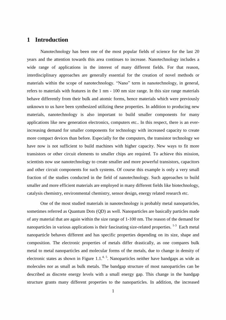
composition. The electronic properties of metals differ drastically, as one compares bulk
metal to metal nanoparticles and molecular forms of the metals, due to change in density of
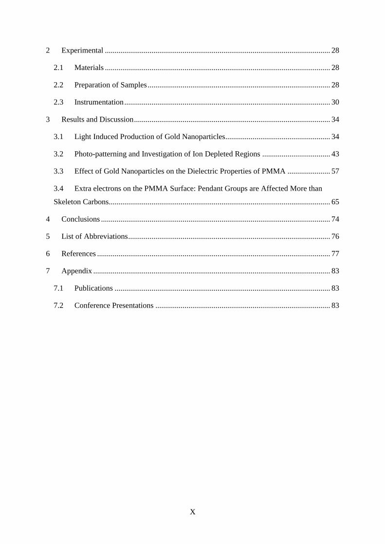
electronic states as shown in Figure 1.1.4, 5
. Nanoparticles neither have bandgaps as wide as
molecules nor as small as bulk metals. The bandgap structure of most nanoparticles can be
described as discrete energy levels with a small energy gap. This change in the bandgap
structure grants many different properties to the nanoparticles. In addition, the increased
2
surface/volume ratio imparts some nanoparticles more reactivity than their bulk counterparts
and enables them to catalyze reactions more efficiently and/or some nanoparticles gain
superior electrical properties making them excellent candidates for the next generation
electronic devices. Of course how their properties change is strongly related to the material
they are made of. Nanoparticles can be synthesized from noble metals atoms like gold,
platinum or silver or transition metals like manganese, iron etc. or even the oxides of the
transition metals. In addition to that, nanoparticles consisting of two or more different metals
can also be synthesized. Core-shell nanoparticles and alloy nanoparticles are examples for this
kind of nanoparticles. Creating such bimetallic (or multimetallic) nanoparticles enables us to
achieve properties that cannot be achieved with monometallic nanoparticles. Whatever they
are made of, the band structure imparted in nanoparticles is particularly important and
enables many applications in electronics3, 6
, optics7, 8
, catalysis9, 10
and biotechnology11, 12
.
Figure 1.1 Evolution of electronic states of a metal from molecule to bulk
As mentioned, nanoparticles of noble metals like gold or silver can be synthesized and
they have exciting chemical, optical and physical properties unlike their bulk metals. For
example, although the bulk form of gold is an inert material, the nanoparticle form of gold is
highly reactive and can catalyze many different reactions. 13-16
Also they have interesting
optical properties. A strong absorption band in visible range is observed for most of these
noble metals, which is called Surface Plasmon Resonance (SPR) band. SPR band is usually a
very strong absorption band which makes the nanoparticles having this band, especially in the
visible range, very valuable for optical applications. In the upcoming chapters, the
extraordinary properties of gold nanoparticles and the applications related to these properties
will be discussed in more detail for a better understanding of the motivation for this work.
.
Molecule Nanoparticle Metal
Band gap
Molecule Nanoparticle Metal
Band gap
3
1.1 Applications of Gold Nanoparticles
Although gold nanoparticles have become popular for the last decade but they are not
newly discovered. They have been used by many cultures from Egypt to China as a colorant
for glass or ceramics throughout the history. We can still admire stained glass windows in
churches colored with colloidal gold from centuries ago. Considering the elapsed time we‟ve
been using gold nanoparticles, the detailed characterization to classify them as nanoparticles
is very recent. After realization of the special electronic structure of gold nanoparticles and
introduction of synthesis methods with excellent control on the particle size and shape, the
research considering the possible applications of gold nanoparticles has increased
tremendously for the last 50 years. Nowadays gold nanoparticles are even being used in some
commercial applications created with certain nanotechnology approaches. There are also
numerous applications of gold nanoparticles in different fields. Brief insights to some of these
fields will be mentioned in the following sections to demonstrate the importance of gold
nanoparticles in science and technology.
1.1.1 Gold Nanoparticles in Electronics
In the electronics, the most demanding objective is to build smaller devices with
higher performance and with less energy consumption. The current semiconductor technology
cannot fulfill these requirements any further since it has reached its physical limit. In place of
the current systems, more capable new materials should be developed. An important
candidate for such technologies is single electron device concept, which uses quantum dots as
its components. The single-electron devices are expected to employ “switchable” quantum
dots and quantum channels with correlated electrons that can offer order of magnitude smaller
components for the new generation electronics. This can result in new generation of
computers, supersensitive electrometers, near infrared receivers and very simple miniature
lasers. Gold nanoparticles can be employed to produce such devices as shown in a study by
Sato et al. in which a single-electron transistor has been constructed using alkanedithiol-
stabilized gold nanoparticles as tunnel junctions.17
When metallic nanoparticles with a diameter in the range of a few nanometers are
arranged with an interparticle distance of about 1nm, they build tunnel junctions with low
electrical capacitances. 18
With this process controlled charge transport between the particles
can be achieved by single-electron tunneling (SET) events at room temperature. SET devices
can range from a single conductive nanoparticle between two microelectrodes to 2D-3D
4
arrays of nanoparticles with SET property in contact with a STM tip. For example, scanning
tunneling spectroscopy has been used to observe SET effects on nanoparticle monolayers of
Au55 nanoparticles in contact with a tip and “Coulomb staircase” behavior (single electron
transfer steps in current-potential curve) was observed even at room temperature and the
capacitance of the nanoparticles was calculated as 3.9 x 10⁻¹⁹
F. 19
Combining many SET
elements to develop computing devices is still challenging. Although construction of single
nanotransistors is not a hard task, combining 1012
transistors to form a transistor network is
yet a dream. But judging from the current studies, gold nanoparticles are excellent candidates
for the components of such devices.
1.1.2 Gold Nanoparticles in Catalysis
Normally gold is known as a chemically inert element and indeed it is one of the most
stable elements. But gold nanoparticles are surprisingly very active catalysts for many
different reactions. For example, Haruta et al. reported that gold nanoparticles dispersed on
Co3O4, Fe2O3 or TiO2 substrates are highly active catalysts for CO and H2 oxidation, NO
reduction, water-gas shift reaction, CO2 hydrogenation and catalytic combustion of methanol.
13-16 This surprising catalytic activity again is a result of the intermediate electronic structure
of gold nanoparticles between bulk metal and atomic state. Catalytic performance can be
sensitive to particle size since the surface structure and electronic properties can change
greatly with the size of the nanoparticles. One of the most important studies about gold
nanoparticle catalysts was by Valden et al. 20
. They produced a highly active model gold
catalyst where gold nanoparticles are spread uniformly on a Ti2O3 surface that showed ~50
fold improvement in the performance of realistic, high surface area catalysts.
Besides improved electronic structure suitable for catalysis, gold nanoparticles are also
preferred as catalysts for their large surface/volume ratio. For catalysis the area of the catalyst
interacting with the substrate is of great importance. For the same amount of catalysts the
ones with larger surface/volume ratio have greater activity than the others if all other
conditions are equal. For this reason generally catalyst species are attached to mesoporous or
microporous structures for heterogeneous catalysis to achieve the largest possible area for
interactions with the substrate. In this aspect, gold nanoparticles serve as a practical solution
for this problem with their easy synthesis and naturally large surface/volume ratio. 1
For instance a final note on catalysis with gold nanoparticles is, as can be realized
from the list of the important reactions that are catalyzed by gold nanoparticles, most of the
5
reactions are related to degradation of harmful gases that cause air pollution and global
warming. For this reason gold nanoparticle based catalyst research is a very hot topic and
better catalysts for the exhaust of the cars or other pollution sources are anticipated in the near
future.
1.1.3 Gold Nanoparticles in Biotechnology
Gold nanoparticles are also widely used in biology and biotechnology for various
applications, mostly on the basis of attaching different groups on nanoparticles and
functionalizing them as sensors or for targeted drug delivery. Currently, DNA-gold
nanoparticle assemblies for biological sensors, gold nanoparticle enhanced immuno-sensing,
gold nanoparticle sugar sensors and other gold nanoparticle bioconjugates like peptides,
lipids, enzymes, drugs and viruses are some of the areas of interests. Conjugates of gold
nanoparticles with oligonucleotides are of great interest because of the potential use of the
programmability of DNA base pairing to organize nanoparticles in space and the multiple
ways of providing a signature for the detection of precise DNA sequences. With these
properties such conjugate systems have many applications in the fields of biosensors, disease
diagnosis and gene expression. 21
22
23
For example, in a study of Mirkin‟s group DNA and
RNA oligonucleotides attached to gold nanoparticles was monitored using surface-enhanced
Raman spectroscopy (SERS) and with the shifts of the corresponding Raman signals
matching with the target oligonucleotides was detected. 24
Like this example, by changing the
attached groups on gold nanoparticles many of the biological molecules could be detected
since biological systems are generally based on pair matching mechanisms. Using this basis,
it is possible to design biosensor chips, consisting of gold nanoparticles with different
recognition groups as an array on the chip and a single drop of specimen can be detected for
many different threads at the same time.
1.1.4 Gold Nanoparticles in Characterization
Gold nanoparticles are also used for the improvement of instrumentation techniques
and detection methods. The mostly known example in this area is SERS effect of gold
nanoparticles. 25
Generally Raman signals of most molecules are hard to detect since the
signals are very weak and the concentration must be very high to conduct a reliable
measurement. But for cases like molecular biology generally the amount of the molecule to be
detected may be very small and some kind of signal enhancement is needed at such cases.

6
Surface plasmon resonance of gold nanoparticles enhances Raman signals and enables non-
detectable amounts of materials to be detected.
Besides, gold nanoparticles can also be used for analytical detection of desired
elements or molecules, changing the attached groups. An example of such studies is given by
Kim et al. for detection of small concentrations (“spectroscopically silent”) of aqueous heavy
metal ions, including toxic metals like lead, cadmium, mercury, was accomplished using
simple calorimetry. 26
In this study, functionalized gold nanoparticles were aggregated in
solution in the presence of divalent metal ions by an ion-templated chelation process and this
caused an easily measurable change in the absorption spectrum of the particles.
7
1.2 Applications of Nanoparticle-Polymer Composites
Polymer composites have been produced and used for decades for various applications.
Probably the most famous and widely used polymer composite is Bakelite, which is a clay
reinforced resin that was developed in the early 20th
century. Nevertheless the true importance
of polymer composites was not fully realized until the end of 20th
century. With the growing
attention towards nanomaterials such as nanoparticles, carbon nanotubes and nanowires, the
investigations towards possible applications of these materials in polymer composites has also
became popular. Addition of nanoparticles or other nanomaterials to the polymer matrix
enables the modification of polymer properties or sometimes implies addition of new
properties to the polymers. These new materials with superior properties have many
applications in different areas like optics, microelectronics, piezoelectrics, batteries, organic
solar cells and biomedical sciences etc. and the application areas still continue to increase.
Some of the most popular applications will be reviewed briefly in this section.
There are several ways to produce polymer-nanoparticle composites depending on the
desired properties and the area of use. Nanoparticles can either be integrated to the polymer
matrix to produce homogeneous composite films or can be capped with polymers to produce
nanoparticle-core/polymer-shell composite nanoparticles. To produce homogeneous
composite films of polymer-nanoparticle composites nanoparticles can either be synthesized
beforehand and integrated to the polymer or can be synthesized within the polymer. For both
cases homogeneous distribution of the pre-synthesized nanoparticles is important. In the
former synthesis method, ligands that are used to stabilize nanoparticles against
agglomeration, can be immiscible with polymer and prevent homogeneous distribution in
some cases. The ligand choice should be carefully made for the synthesis of nanoparticles for
that reason. However in the latter case, which is the synthesis of the nanoparticles directly
within the polymers, the homogeneous distribution of nanoparticles in polymer is granted for
most cases. Comparing the distribution of metal pre-cursors to nanoparticles, the distribution
of metal pre-cursors can be more easily achieved because of their small size and high
miscibility with the polymer.
Another important criterion to be watched for the nanoparticle-polymer composites is
maintaining the interaction and full integration of nanoparticles in the polymer matrix. In this
case ligands around the nanoparticles can again be a problem since even if the ligand is
8
miscible with polymer and enables homogeneous distribution, it still forms a barrier between
nanoparticle and polymer. Especially in applications for electronics, full integration of
nanoparticles with the polymer is needed for improved electron transfer between
nanoparticles and polymer. For this reason ligand hinderance should be kept at a minimum.
The synthesis of nanoparticles inside polymer matrices is again advantageous for such cases
since the nanoparticles synthesized with this method in the polymer don‟t need ligands for the
stabilization. Polymer maintains the particle size of nanoparticles and prevents them against
agglomeration by its limited pore size and low diffusion rate within. For that reason better
interaction of polymer with nanoparticle can be maintained using this synthesis technique.
One of the most important effects of nanoparticles on polymer materials is changing
their optical properties. For example, the addition of nanoparticles can change the refractive
index of the polymers, as shown by many different studies27-32
. TiO2 is one of the most widely
used materials to modify the refractive index of the polymers, but there are also studies
employing ZrO2, Al2O2, ZnO and PbS for this purpose. The modification of refractive index
of polymers is especially important for applications like microoptics and optical data
transmission. Photoluminescence of nanocomposites is another interesting property of
nanoparticle-polymer composites and it has a high potential for applications. For example
epoxy nanocomposites containing ZnO nanoparticles can be used as solid state lightning33
and
ZnO-polymer core-shell nanoparticles can be used for in vitro cell imaging34
.
Combination of Fe2O3, Fe3O4 or ferrite nanoparticles with polymers creates the
opportunity to produce polymeric materials with magnetic properties. Polymer
nanocomposites with desired magnetic properties free of hysteresis at room temperature and
in some cases transparent can be produced this way.35, 36
For polymers with magnetic
properties there are many potential applications in different fields such as in industry; as
microwave absorbing material37
, as contrast agent for magnetic resonance imaging38, 39
, in
cancer treatment by local hyperthermia40, 41
, as drug carriers42, 43
or as biocompatible
ferromagnetic fluid44, 45
.
Polymer composites with interesting dielectric properties can be synthesized with the
addition of conductive metal nanoparticles to polymers. The most aspiring advantage of using
polymer composites as parts of integrated circuits is the opportunity of “printing” the
polymers on the boards to create these circuits. Such an opportunity would bring down the
production costs tremendously compared to the current technology. Also polymers can be
synthesized with low cost methods and there is practically unlimited amount of resources
9
compared to the limited resources of silicon, which is used as the base material of the current
electronic devices. Additionally light and flexible devices can be produced using polymer
composites as the main material which is an advantage regarding the preferences of the
consumers towards such products. Studies continue to grow aiming to produce suitable
nanocomposites as components for electronic applications. 3, 46
For example there are many
attempts to design materials with high permittivity to be used as capacitors. BaTiO3
composites with polymers are promising candidates for such applications because of the high
permittivity of BaTiO3. 47, 48
In another study the capacitive and resistive characteristics of
ionic polymer metal composites are discussed in length. 49
Although there are encouraging
examples of polymer composites demonstrating excellent capacitance or conductance abilities
for the design of circuit components, the integration of those into circuits and devices still has
a long way to go and studies will continue to overcome many hardships in this way.
Another important potential application field for the polymer-nanoparticle composites is
employing them as electrodes in lithium-ion batteries. Nanocomposites based on inorganic
nanoparticles and carbon are very advantageous as anode materials in lithium-ion-batteries
and are expected to increase the performance of the batteries significantly since reducing
dimensions using nanomaterials increases the diffusion rate of lithium insertion and removal
due to short diffusion lengths. 50
Also the electron transfer between nanoparticles is enhanced
and the high surface/volume ratio enables high contact area with the electrolytes.
Nanocomposites containing SnO2 seems very promising as anode materials since they have
higher specific capacities than the standard carbon anodes. The most important point to
improve about nanocomposite anodes is the cyclability of the anode. The current cyclability
of the nanocomposites are quite low comparing to the current systems and studies to improve
this problem continue. Combining nanoparticles with carbon based materials gives promising
results for increasing the number of cycles the anode can go through. Zhang et al.
demonstrated a high number of cycles (100 cycles with 34% decay) for metallic Sn
nanoparticles encapsulated in an elastic carbon sphere. 51
Carbon encapsulation of SnO2 also
results in high reversible specific capacity according to a study by Park et al. 52
10
1.3 Synthesis of Nanoparticles
Synthesis methods for nanoparticles are typically grouped into two categories: (i) top-
down and (ii) bottom-up approaches. The top-down approach involves division of a bulky
solid into smaller portions, using milling, chemical methods and volatilization of a solid
followed by condensation of the volatilized components. The bottom-up approach uses
condensation of atoms or molecular species from the gas phase or the solution. Both methods
have advantages and disadvantages in different aspects. The top-down approach employing
lithography and etching techniques can advantageously be used to generate required
nanostructures in a spatially controlled manner. This property is important for integration and
interconnection of nanoparticles into circuit elements and/or to design other specific
applications. On the other hand, the bottom-up approach is very powerful in creating
monodisperse nanoparticles with atomic precision and this precise synthesis is important for
applications in need of well-defined nanoparticles. Also the machinery and the costs of both
approaches differ considerably. For the top-down techniques generally expensive machinery
and careful maintenance are needed. While for the bottom-up techniques, reactions generally
take place in a test tube and the cost of reagents are a lot cheaper compared to the costs of
machinery used in the top-down approach. There are strong and weak sides of both
approaches and one would select the most suitable method for their own application.
1.3.1 Synthesis of Gold Nanoparticles in the Solution Phase
As mentioned before, nanoparticles can be produced with many different techniques,
gold nanoparticles are no exception to that. Nevertheless solution phase synthesis is the most
commonly used synthesis approach for gold nanoparticles, because of its well defined nature
and the accuracy of the synthesized nanoparticles.1, 53
The solution phase synthesis generally
consists of two steps; reduction of gold salt ions in the solution with a mild reducing agent
and capping the nanoparticles with an organic molecule to prevent the further agglomeration
of the particles. The reducing agent reduces Au3+
ions to Au0 atoms and Au
0 atoms coalesce
to form nanoparticles since they are thermodynamically more stable. To prevent further
aggregation of the formed nanoparticles, organic capping agents are used to result in stable
and dispersed nanoparticles.
Among the commonly used synthesis methods of gold nanoparticles the most popular
one is Turkevitch method, introduced by Turkevitch in 1951.54
The Turkevitch method
11
employs citrate reduction of HAuCl4 in water. Gold nanoparticles of about 10-30 nm can be
synthesized with this method. Also a method for the synthesis of nanoparticles with pre-
chosen size was introduced by Frens in 1973. 55
It was shown that the derivation of the ratio
between the reducing/stabilizing agents can lead to nanoparticles size between 16 nm – 147
nm size range. Turkevitch synthesis is generally used to produce nanoparticles with a loose
shell of ligands (citrate ions) around the gold nanoparticle core.
Another method used widely for gold nanoparticle synthesis is the Brust-Schiffrin
method. 56, 57
This method was proposed in 1994 and had quite an impact on the field since it
enabled the facile synthesis of thermally stable and air-stable gold nanoparticles with reduced
dispersity and controlled size for the first time. Nanoparticles synthesized by this method can
be repeatedly isolated and redissolved in common organic solvents without aggregation and
decomposition so they can be easily handled like stable organic molecules. This synthesis
method uses thiol ligands that strongly bind gold, because of the soft character of both gold
and sulfur. AuCl4- is transferred to toluene using tetraoctylammonium bromide as the phase
transfer agent and reduced by NaBH4 in the presence of dodecanethiol. The color of organic
phase changes from orange to deep brown within a few seconds upon the addition of NaBH4.
Gold nanoparticles synthesized with this method are in the size range of 1 nm – 3 nm, the size
of the nanoparticles can be controlled adjusting the gold/thiol ratio and also the temperature of
the reaction medium. Fast reductant addition and cooled solutions produce smaller and more
monodispersed nanoparticles with this method.
Other than the synthesis methods mentioned above there are many other methods to
produce gold nanoparticles with pre-chosen size and morphology. In these methods the size
and shape of the nanoparticles are generally controlled by changing the medium temperature,
the concentration of gold salt, the concentration of the reducing agent, adding reactants slower
or faster or by variation of stirring conditions.
Thus, using solution phase synthesis methods, particle size, composition and life-time
of nanoparticles may be controlled very accurately. However integration of the synthesized
nanoparticles into solid materials like polymers or films is a big problem for this synthesis
method if one wants to produce nanoparticle-polymer composites. Especially the spatial
control on the distribution of nanoparticles throughout the polymer matrix is very hard using
this synthesis method.
12
1.3.2 Synthesis of Nanoparticles in Polymer Matrix
Polymer-nanoparticle composites are important candidates for new age technological
devices as mentioned in the previous sections and ongoing research by many different groups
is performed for production and characterization of these systems. Polymers can be used as
platforms to support gold nanoparticles as substrates. For example, in many biological
applications polymers are used as carrying media for nanoparticles to their targets, or in
catalysis polymers can be used as supports for nanoparticle catalysts. As much as polymers
are good candidates for supporting nanoparticles, nanoparticle-polymer composites can also
be functionalized to produce new materials using both properties of gold nanoparticles and
polymers. Flexible, low weight, advanced electronic devices can be designed using such
materials in the production. But as mentioned before the primary problem that we must
overcome to produce such systems is the integration of nanoparticles in to the polymers
homogeneously and for some applications with a spatially controlled manner.
Nanoparticles may be synthesized before the integration to polymer or within the
polymer to produce composite systems. For example, Vitale et al.58
synthesized Au
nanoparticles and dispersed these dodecanethiol functionalized Au nanoparticles, in
poly[platinum-bis(tributhylphosphine) diethynylbiphenyl] afterwards, whereas Horiuchi et al.
demonstrated that Pd nanoparticles may be produced in polymethylmethacrylate films,
through adsorption of Pd(acac)2 vapor to irradiated polymer films.59
With the method
proposed by Horiuchi et al. patterned polymer films of diblock-co-polymers or polymer
blends can be produced using the varying adsorption tendencies of Pd(acac)2 vapor to
different polymers. However, this process needs high temperature conditions (180oC) for the
evaporation of Pd metal into the polymer matrix thus is not appropriate for systems working
at room temperature.
At room temperature, an efficient approach, used for the production of nanoparticles
within the polymer matrix is employment of irradiation. Energetic light is a widely used
element to produce electrons within in the synthesis medium for reduction of metal salts and
it is both used in the solution phase synthesis as well as, in the solid state synthesis. Gachard
et al. has reported a synthesis method, which employs γ-rays to induce reduction in an
aqueous solution of 2-propanol and polyvinyl alcohol with gold salt.60
In another study, we
reported that x-rays can also be used to reduce gold ions into gold atoms followed by
formation of gold nanoparticles61
. Not only highly energetic light like γ-rays and x-rays are
employed for reduction, but also less energetic UV irradiation can also be used for this
13
purpose. Korchev et al. proposed that silver nanoparticles can be produced in sulfonated
poly(ether−ether)ketone−poly(vinyl alcohol) films by direct irradiation with 350 nm UV
light62
. Alexandrov et al. used UV light to initiate the gold nanoparticle growth in PMMA
films and finalized the synthesis by annealing the samples at different temperatures from 20oC
up to 80oC
63.
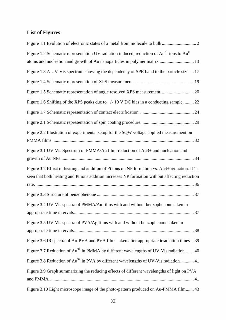
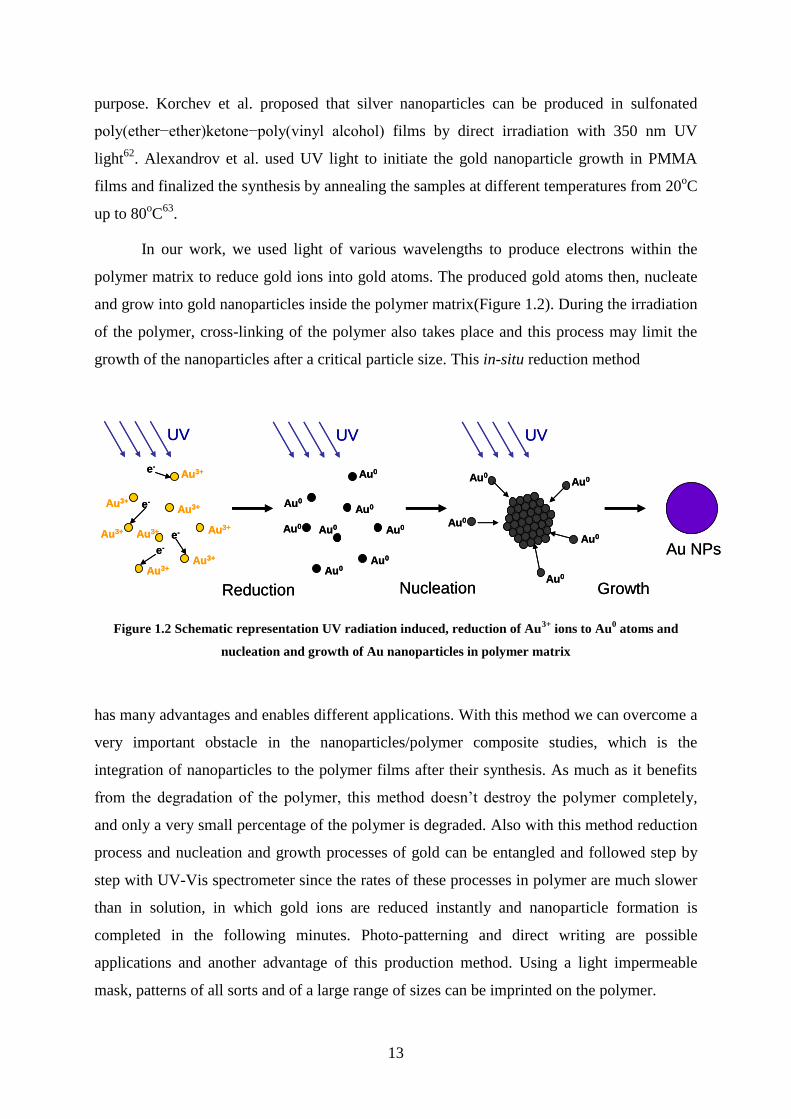
In our work, we used light of various wavelengths to produce electrons within the
polymer matrix to reduce gold ions into gold atoms. The produced gold atoms then, nucleate
and grow into gold nanoparticles inside the polymer matrix(Figure 1.2). During the irradiation
of the polymer, cross-linking of the polymer also takes place and this process may limit the
growth of the nanoparticles after a critical particle size. This in-situ reduction method
Figure 1.2 Schematic representation UV radiation induced, reduction of Au3+
ions to Au0 atoms and
nucleation and growth of Au nanoparticles in polymer matrix
has many advantages and enables different applications. With this method we can overcome a
very important obstacle in the nanoparticles/polymer composite studies, which is the
integration of nanoparticles to the polymer films after their synthesis. As much as it benefits
from the degradation of the polymer, this method doesn‟t destroy the polymer completely,
and only a very small percentage of the polymer is degraded. Also with this method reduction
process and nucleation and growth processes of gold can be entangled and followed step by
step with UV-Vis spectrometer since the rates of these processes in polymer are much slower
than in solution, in which gold ions are reduced instantly and nanoparticle formation is
completed in the following minutes. Photo-patterning and direct writing are possible
applications and another advantage of this production method. Using a light impermeable
mask, patterns of all sorts and of a large range of sizes can be imprinted on the polymer.
Au0Au0
Au0
Au0
Au0
Au NPs
Au3+
Au3+Au3+
Au3+
Au3+Au3+
Au3+ Au3+
Au0
Au0Au0
Au0
Au0Au0
Au0 Au0
UV UV UV
Reduction Nucleation Growth
e-
e-
e-
e-
Au0Au0
Au0
Au0
Au0
Au NPs
Au3+
Au3+Au3+
Au3+
Au3+Au3+
Au3+ Au3+
Au0
Au0Au0
Au0
Au0Au0
Au0 Au0
UV UV UV
Reduction Nucleation Growth
e-
e-
e-
e-
14
1.4 Advantages of Poly(methyl methacrylate) as a Synthesis Medium
PMMA is a well known, utilized and extensively studied polymer, which is an
important dielectric element in electronics. One of the advantages of using PMMA as a
substrate is the ease of processibility and preparation of PMMA films. PMMA can be
dissolved in acetone relatively easier compared to the dissolution of other polymers in their
particular solvents. Acetone was selected as the solvent since it can both dissolve PMMA and
HAuCl4 and is not as hazardous as other organic solvents. Film preparation with acetone is
also fast and easy since acetone can evaporate at room temperature very quickly compared to
many other solvents.
Besides the ease of preparation, PMMA is also appropriate for its stability. PMMA
matrix is more rigid compared to many other polymers, hence nanoparticles can be confined
to specific sites after their preparation within the matrix. For example, PVA was also used in
our studies in earlier stages and for specific purposes and gold nanoparticles can also be
prepared in PVA matrices, but our experiences showed us that PVA films containing gold
nanoparticles were not as stable as PMMA films. There were also reports concerning this fact
in the literature. 64
After their preparation PMMA films conserve their spectroscopic
properties for a long time (3 years of stability was observed until now). For PVA films change
in the absorption of surface plasmon resonance band was observed after 1 year and distortion
on the photo-patterns printed on PVA was also observed. On the other hand, photo-patterns
printed at PMMA films were stable.
15
1.5 Photo-Patterning of Polymer Composites
Patterning of polymer composites is a technologically important process for many
different applications. In polymer-nanoparticle composite preparation, besides being able to
achieve homogeneous distribution of nanoparticles inside polymer films for successful
composites, pattern creation on or in polymer films using nanoparticles is another important
issue, especially for optical and electronic applications. There are many different techniques
employed to create patterned polymer films. One of the most used techniques for achieving
patterns, consisting of regions with and without nanoparticles, is to use the immiscibility of
various polymer blends to selectively adsorb nanoparticles in one of the immiscible polymers.
In such a study Horiuchi et al. demonstrated the selective reduction Pd(acac)2 vapors by
poly(styrene)(PS) matrix in PMMA-PS blends. 59
They subjected PS-PMMA blends to
Pd(acac)2 vapor in N2 atmosphere, the blend adsorbed Pd vapor and only PS matrix
selectively reduced Pd ions to Pd nanoparticles because of the PS‟s high reduction power
towards Pd ion. PMMA matrix on the other hand didn‟t produce any Pd nanoparticles since
the reduction power of PMMA is rather low. This study showed with selective production of
Pd nanoparticles by different polymers in a blend, one can produce patterned films according
to the blend‟s structure. Nevertheless the control on the pattern morphology is very hard to
achieve with such a technique. In another study, Horiuchi et al. found a way to increase
PMMA reducing power externally to modify the printed patterns. 65
In which they subjected
PMMA films to UV irradiation for an increased reduction power of PMMA towards adsorbed
Pd ions and with this method they produced patterns consisting of UV irradiated Pd
nanoparticles containing regions and non-irradiated Pd ion containing regions.
Another technique that can be used to achieve such patterns on polymer films is to
start with a dispersed metal precursor and selectively reducing required regions for the pattern
to produce nanoparticles within. 66
This technique is the one we used to produce patterns
consisting of regions with and without gold nanoparticles within the PMMA matrix. With this
technique using a photomask impermeable to light, any pattern can be printed on the polymer
films consisting of regions with and without nanoparticles. The stability of the printed
patterns is an important issue in this technique and the production of stable patterned films
was achieved and this issue will be discussed in the upcoming chapters.
16
1.6 Ultraviolet-Visible Spectroscopy
Ultraviolet-Visible (UV-Vis) spectroscopic technique measures the absorption spectra
of samples in the ultraviolet and visible range of the electromagnetic spectrum by recording
the amount of light adsorbed by the sample in different wavelengths. The absorption spectra
in this range include electronic transitions which are generally the transition of an electron
from a ground state to an excited state in the molecular orbitals. In addition, some vibrational
transitions may also be observed when the spectrum is of a gas phase molecule. The
electronic transitions observed in the UV-Vis spectroscopy generally appear as broad peaks
because of the interactions of molecules with each other and the solvent molecules. For
example the UV-Vis spectrum of a molecule dissolved in water, generally includes the effects
of hydrogen bonding and molecular interactions in addition to its own electronic transitions.
To get rid of this broadening is only possible if the spectrum is recorded in gas phase and/or
in inert matrices, but this may not be possible for many samples.
UV-Vis spectroscopy is a widely used technique since it‟s very easy to use and
relatively cheap compared to many other techniques and can give valuable information for
different types of samples. The most fundamental formulation used in UV-Vis spectroscopy
for the quantification of measured absorption values is the Beer-Lambert law:
In this formulation, A is the measured absorbance at a specific wavelength, is the molar
absorptivity or extinction coefficient at a specific wavelength, b is the path-length through the
sample and C is the concentration of the absorbing species. Thus, one can calculate the
concentration of the absorbing species in a sample by simply measuring the absorption of the
sample and using the molar absorptivity at a specific wavelength. Of course the only
information UV-Vis provides about the sample is not its concentration. At least, the
applications of UV-Vis spectroscopy in nanotechnology are more. Especially, in the
nanoparticle characterization UV-Vis spectroscopy is widely used for the determination of
many different properties. For example, for quantum dots, the UV-Vis spectroscopy can be
used to calculate the average particle size and more importantly the band-gap of the
nanoparticles. The particle size has an important role in the determination of the absorption
spectrum in UV-Vis range, since, even though the material which makes up a nanoparticle,
defines its intrinsic energy signature, the effect of nanoparticle's size significant at energies
near the bandgap. The noble metal nanoparticles like gold or silver are also no exceptions.
17
They have distinct surface plasmon resonance bands in the visible region, which gives them
their characteristic color. Surface plasmon resonance band will be discussed in length in the
following section.
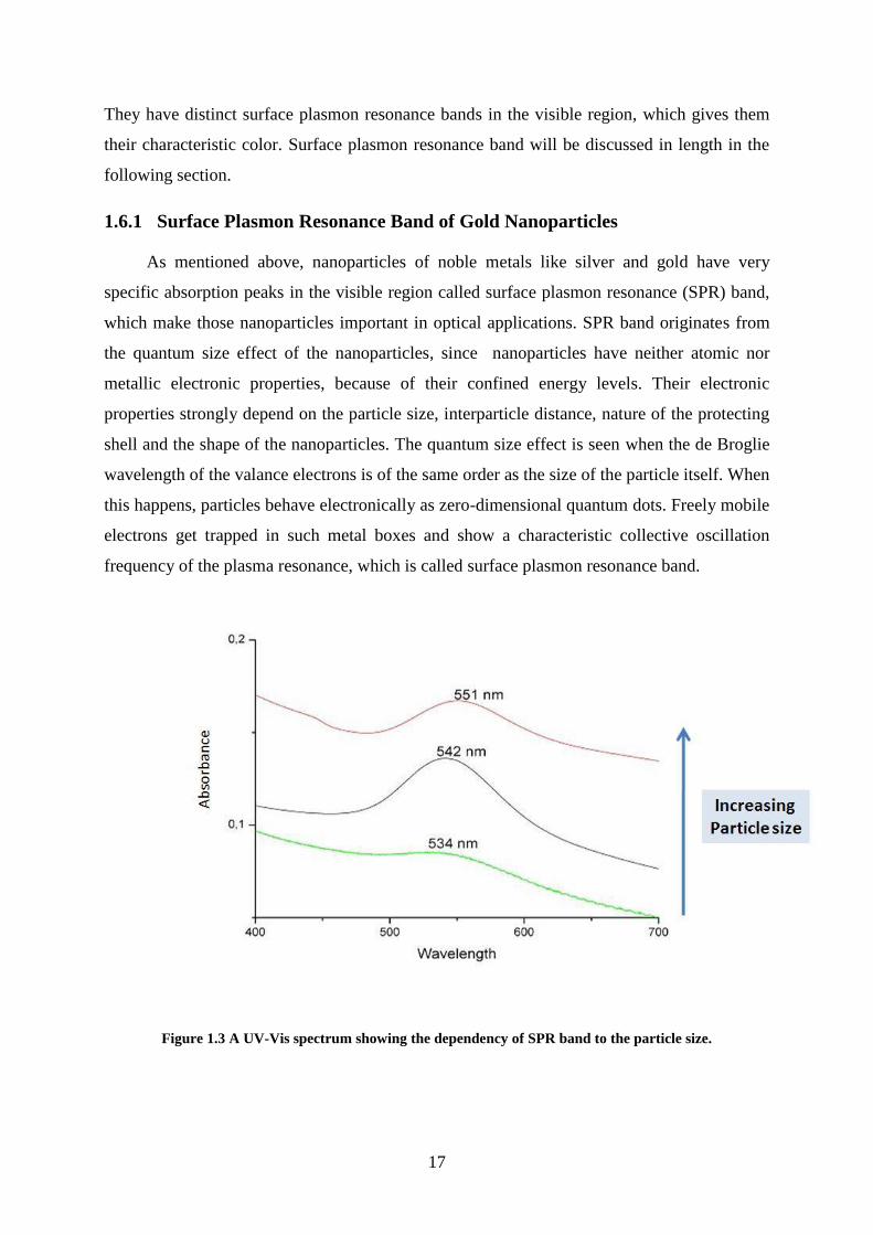
1.6.1 Surface Plasmon Resonance Band of Gold Nanoparticles
As mentioned above, nanoparticles of noble metals like silver and gold have very
specific absorption peaks in the visible region called surface plasmon resonance (SPR) band,
which make those nanoparticles important in optical applications. SPR band originates from
the quantum size effect of the nanoparticles, since nanoparticles have neither atomic nor
metallic electronic properties, because of their confined energy levels. Their electronic
properties strongly depend on the particle size, interparticle distance, nature of the protecting
shell and the shape of the nanoparticles. The quantum size effect is seen when the de Broglie
wavelength of the valance electrons is of the same order as the size of the particle itself. When
this happens, particles behave electronically as zero-dimensional quantum dots. Freely mobile
electrons get trapped in such metal boxes and show a characteristic collective oscillation
frequency of the plasma resonance, which is called surface plasmon resonance band.
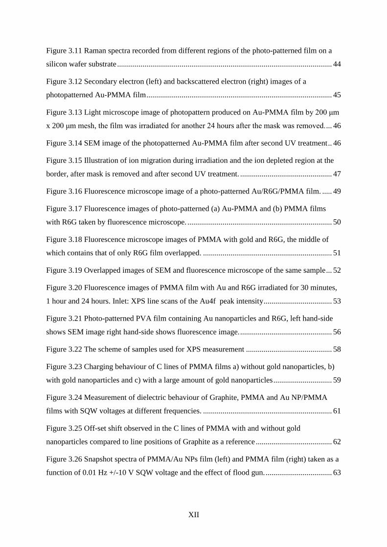
Figure 1.3 A UV-Vis spectrum showing the dependency of SPR band to the particle size.
18
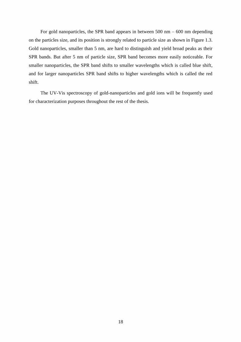
For gold nanoparticles, the SPR band appears in between 500 nm – 600 nm depending
on the particles size, and its position is strongly related to particle size as shown in Figure 1.3.
Gold nanoparticles, smaller than 5 nm, are hard to distinguish and yield broad peaks as their
SPR bands. But after 5 nm of particle size, SPR band becomes more easily noticeable. For
smaller nanoparticles, the SPR band shifts to smaller wavelengths which is called blue shift,
and for larger nanoparticles SPR band shifts to higher wavelengths which is called the red
shift.
The UV-Vis spectroscopy of gold-nanoparticles and gold ions will be frequently used
for characterization purposes throughout the rest of the thesis.
19
1.7 X-Ray Photoelectron Spectroscopy
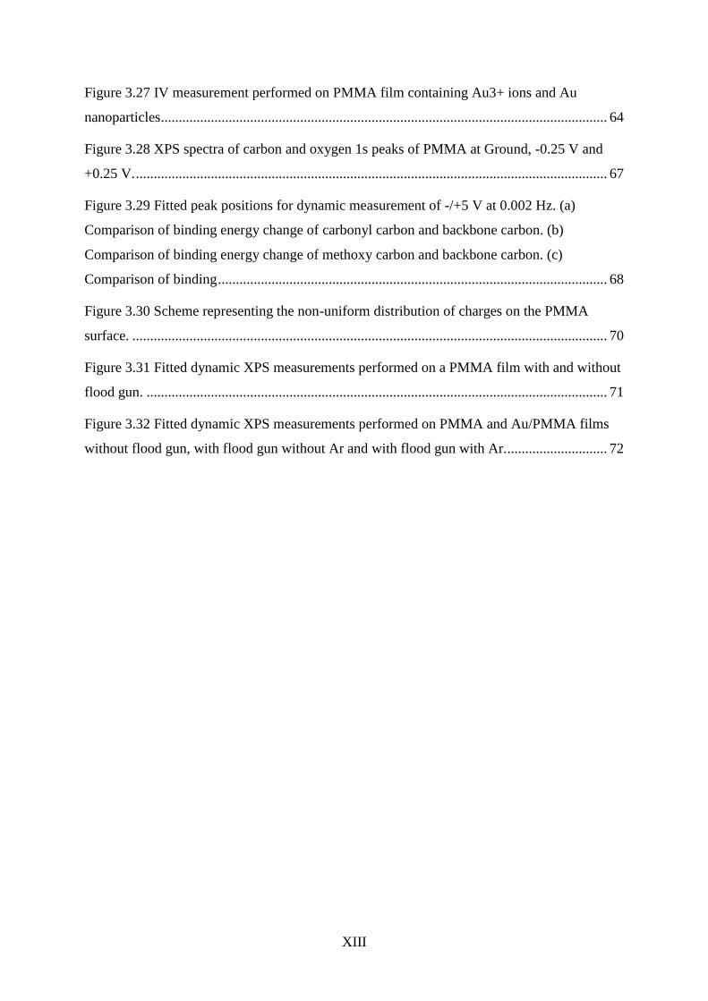
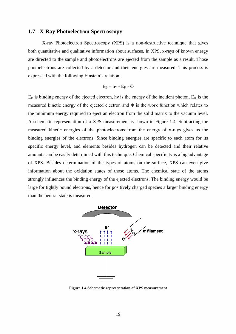
X-ray Photoelectron Spectroscopy (XPS) is a non-destructive technique that gives
both quantitative and qualitative information about surfaces. In XPS, x-rays of known energy
are directed to the sample and photoelectrons are ejected from the sample as a result. Those
photoelectrons are collected by a detector and their energies are measured. This process is
expressed with the following Einstein‟s relation;
EB = hν - EK - Φ
EB is binding energy of the ejected electron, hν is the energy of the incident photon, EK is the
measured kinetic energy of the ejected electron and Φ is the work function which relates to
the minimum energy required to eject an electron from the solid matrix to the vacuum level.
A schematic representation of a XPS measurement is shown in Figure 1.4. Subtracting the
measured kinetic energies of the photoelectrons from the energy of x-rays gives us the
binding energies of the electrons. Since binding energies are specific to each atom for its
specific energy level, and elements besides hydrogen can be detected and their relative
amounts can be easily determined with this technique. Chemical specificity is a big advantage
of XPS. Besides determination of the types of atoms on the surface, XPS can even give
information about the oxidation states of those atoms. The chemical state of the atoms
strongly influences the binding energy of the ejected electrons. The binding energy would be
large for tightly bound electrons, hence for positively charged species a larger binding energy
than the neutral state is measured.
Figure 1.4 Schematic representation of XPS measurement
e-
x-rays
Sample
Detector
e-
e- filamente-e-
x-raysx-rays
Sample
Detector
e-
e- filament
e-e-
e- filament
20
XPS is also a very surface sensitive technique. X-rays can penetrate through microns
of depth into the sample, but ejected electrons without energy lost can only come from the top
10 nm or less (depending on the type of material the sample is made of) of the sample because
the photoelectrons cannot travel through larger distances without loss of energy. To have
information from depths deeper than 10 nm x-rays with high energies should be used and
such measurements can be performed only at synchrotron facilities. Conventional XPS
instruments usually work with x-rays at two different energies, Al Kα has 1486.6 eV and Mg
Kα has 1253.6 eV x-ray energies.
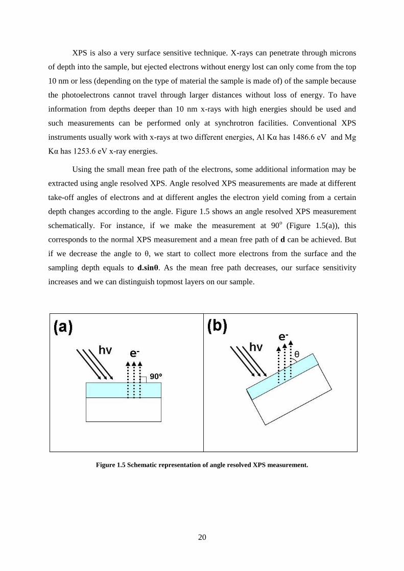
Using the small mean free path of the electrons, some additional information may be
extracted using angle resolved XPS. Angle resolved XPS measurements are made at different
take-off angles of electrons and at different angles the electron yield coming from a certain
depth changes according to the angle. Figure 1.5 shows an angle resolved XPS measurement
schematically. For instance, if we make the measurement at 90o
(Figure 1.5(a)), this
corresponds to the normal XPS measurement and a mean free path of d can be achieved. But
if we decrease the angle to θ, we start to collect more electrons from the surface and the
sampling depth equals to d.sinθ. As the mean free path decreases, our surface sensitivity
increases and we can distinguish topmost layers on our sample.
Figure 1.5 Schematic representation of angle resolved XPS measurement.
21
1.7.1 Using Charging as a tool in XPS
In XPS measurements, a current is generated by the flow of photoelectrons and
secondary electrons from the sample to the vacuum. Normally, the generated charge on the
surface of the sample is neutralized by the electrons coming from the ground and no effect of
this charging is seen through the measurements. But if the sample is non-conducting, the
neutralization of the surface charging cannot be achieved and shifts at line positions are
observed during the measurements, because of the charging. In the early years of XPS
experiments, the charging of non-conducting samples had been considered as a nuisance and
many successful techniques were developed to overcome this problem. For example, an
electron filament can be added to the system to generate extra low energy electrons for the
sample to ease the neutralization as shown in Figure 1.4.
Indeed charging phenomena causes shifts in the binding energies and inconsistent
results can be produced. But it is also proved to be true that when used correctly, additional
information about the samples can be harvested using charging as a tool. Applying external
voltage bias to the sample during a XPS measurement causes shifts in the positions depending
to the nature of the sample. For conducting samples positions shift as much as the applied
bias, but for non-conducting samples the shift is observed to be nonlinear due to charging.
This nonlinear behavior contains additional molecular and structural information. For
example, it was shown by Ulgut et al.,67
that the thickness of SiO2 films on Si substrates can
be measured, with the application of positive and negative biases to the sample. Also in
another paper the structure of a composite film was extracted again using charging as a tool
for extracting additional information.68
One way to use charging in XPS is applying a DC bias to sample at various voltages.
For conducting samples if +10 V is applied to the sample an exact 10 eV shift towards higher
binding energy is observed for its corresponding lines, this process is shown in Figure 1.6. If
we have a non-conducting sample, according to its charging properties a smaller shift is
observed in its line positions. This result points out the accumulated negative charge on the
surface. When positive 10 V is applied to the non-conducting sample, the line position shifts
+10 eV, but the positive potential on the surface attracts more low energy electrons from its
surroundings than normal, thus the line positions start to shift to lower binding energies
depending on the resistance of the sample. Overall, line shifts are smaller than the applied
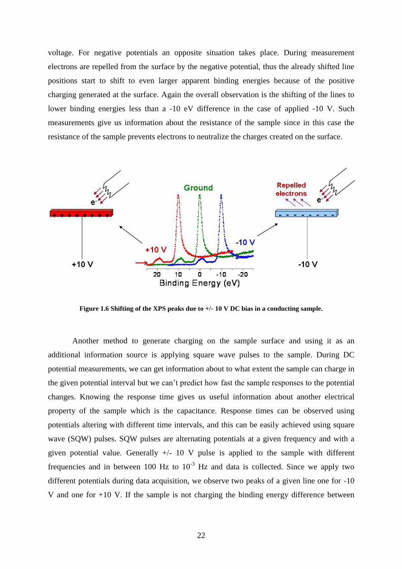
22
voltage. For negative potentials an opposite situation takes place. During measurement
electrons are repelled from the surface by the negative potential, thus the already shifted line
positions start to shift to even larger apparent binding energies because of the positive
charging generated at the surface. Again the overall observation is the shifting of the lines to
lower binding energies less than a -10 eV difference in the case of applied -10 V. Such
measurements give us information about the resistance of the sample since in this case the
resistance of the sample prevents electrons to neutralize the charges created on the surface.
Figure 1.6 Shifting of the XPS peaks due to +/- 10 V DC bias in a conducting sample.
Another method to generate charging on the sample surface and using it as an
additional information source is applying square wave pulses to the sample. During DC
potential measurements, we can get information about to what extent the sample can charge in
the given potential interval but we can‟t predict how fast the sample responses to the potential
changes. Knowing the response time gives us useful information about another electrical
property of the sample which is the capacitance. Response times can be observed using
potentials altering with different time intervals, and this can be easily achieved using square
wave (SQW) pulses. SQW pulses are alternating potentials at a given frequency and with a
given potential value. Generally +/- 10 V pulse is applied to the sample with different
frequencies and in between 100 Hz to 10-3
Hz and data is collected. Since we apply two
different potentials during data acquisition, we observe two peaks of a given line one for -10
V and one for +10 V. If the sample is not charging the binding energy difference between
23
these two peaks can be observed as 20 eV. But in the case of charging the binding energy
difference between these two peaks starts to decrease with the increase in charging.
Basically the working principle behind the SQW potential and the DC potential
measurements is the same. But for SQW potential measurements, additionally we can have
information about capacitance property of the sample as mentioned before. The reason for
that is in the case of SQW we can switch between negative and positive potential with a given
frequency, thus we can see how quick the sample responses to the change of the potential in
the frequency range we apply. For example, at high frequencies like 100 Hz, the potential
switches from -10 V to +10 V so quickly that our polymeric samples cannot follow them , as
a result we see no charging changes and observe an exact 20 eV binding energy difference,
even though the sample itself maybe is in a charged state. Samples cannot find enough time to
build up charge on them at frequencies so high. But for example, at frequencies like 10-2
Hz
the potential switches from negative to positive at every 100 seconds, so the sample has
enough time to build up charge and we can see binding energy differences smaller than 20 eV
at such frequencies for non-conducting polymeric samples. The charge build up is of course
different for every sample since this property depends on the dielectric properties of the
sample, for example using this difference we can obtain capacitance for these samples by
taking measurements at different frequencies and following the trend of each sample. At very
low frequencies like 10-4
or 10-5
Hz the binding energy difference reaches to a point where it
doesn‟t decay anymore and this point gives us the same binding energy difference as the DC
potential measurements give. So SQW measurements give us information both on resistance
and on capacitance of the sample.
24
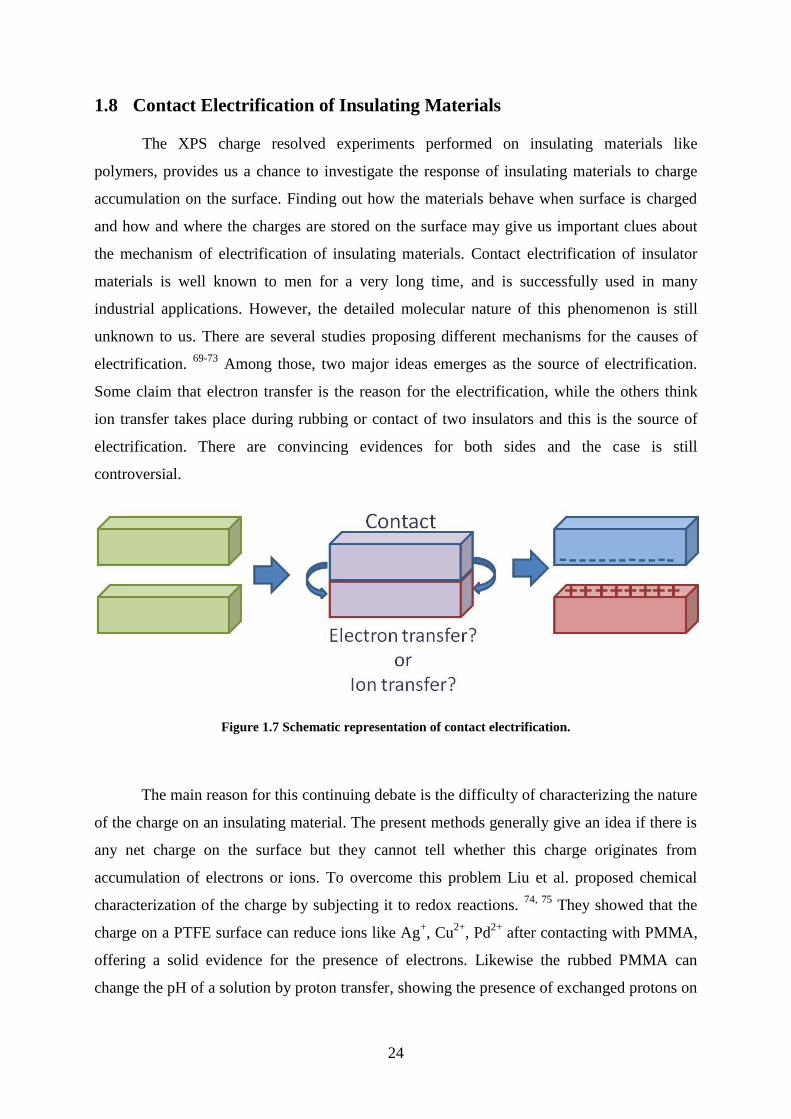
1.8 Contact Electrification of Insulating Materials
The XPS charge resolved experiments performed on insulating materials like
polymers, provides us a chance to investigate the response of insulating materials to charge
accumulation on the surface. Finding out how the materials behave when surface is charged
and how and where the charges are stored on the surface may give us important clues about
the mechanism of electrification of insulating materials. Contact electrification of insulator
materials is well known to men for a very long time, and is successfully used in many
industrial applications. However, the detailed molecular nature of this phenomenon is still
unknown to us. There are several studies proposing different mechanisms for the causes of
electrification. 69-73
Among those, two major ideas emerges as the source of electrification.
Some claim that electron transfer is the reason for the electrification, while the others think
ion transfer takes place during rubbing or contact of two insulators and this is the source of
electrification. There are convincing evidences for both sides and the case is still
controversial.
Figure 1.7 Schematic representation of contact electrification.
The main reason for this continuing debate is the difficulty of characterizing the nature
of the charge on an insulating material. The present methods generally give an idea if there is
any net charge on the surface but they cannot tell whether this charge originates from
accumulation of electrons or ions. To overcome this problem Liu et al. proposed chemical
characterization of the charge by subjecting it to redox reactions. 74, 75
They showed that the
charge on a PTFE surface can reduce ions like Ag+, Cu
2+, Pd
2+ after contacting with PMMA,
offering a solid evidence for the presence of electrons. Likewise the rubbed PMMA can
change the pH of a solution by proton transfer, showing the presence of exchanged protons on
25
the surface. Supporting Liu et al. suggestion, Jacobs et al. show that there is no detectable
material transfer during contact electrification, regardless of the ion transfer claims, and they
propose, proton transfer occurs between carboxylic acid groups of PDMS and carbonyl
groups of PMMA during contact. 69, 76
On the other hand, McCarthy et al. claim that electron
transfer is not energetically plausible, since it involves many demanding processes like
removing an electron from a material, transferring it through separation of charge across an
interface and adding an electron to another material and these processes can occur at room
temperature for only materials with zero bandgap. 73, 77
They proposed that ion transfer is the
source of contact electrification for insulating electrets. Likewise Diaz et al. nominated ions as
the source of charge during contact electrification and constructed a model explaining the role
of ions during charging process on polymers. 70, 78, 79
Understanding the reason of contact electrification process is important for the
advancement of many applications and preventing problems arising from the contact
electrification. Understanding of electrification process is also important for the development
of electroactive polymers and elastomers. In a recent article by Carpi et al. the importance of
dielectric elastomer actuators for applications like touch screens for consumer electronics and
artificial muscles. 80
As shown by Brochu et al. artificial muscles can exceed the performance
of natural muscles using dielectric elastomers. 81
One other application possibility, mentioned
by Carpi et al. is using dielectric elastomer transduction in reverse way and producing
electrical energy from the mechanical energy, which would be groundbreaking if applicable.
A better understanding of the electrification process will definitely help realization of such
applications and should be pursued. Therefore, within the scope of this thesis, XPS is used for
the purpose, hoping that with its chemical specificity, and at the same time being sensitive to
charge accumulation/dissipation may offer new insight(s) at the molecular level.
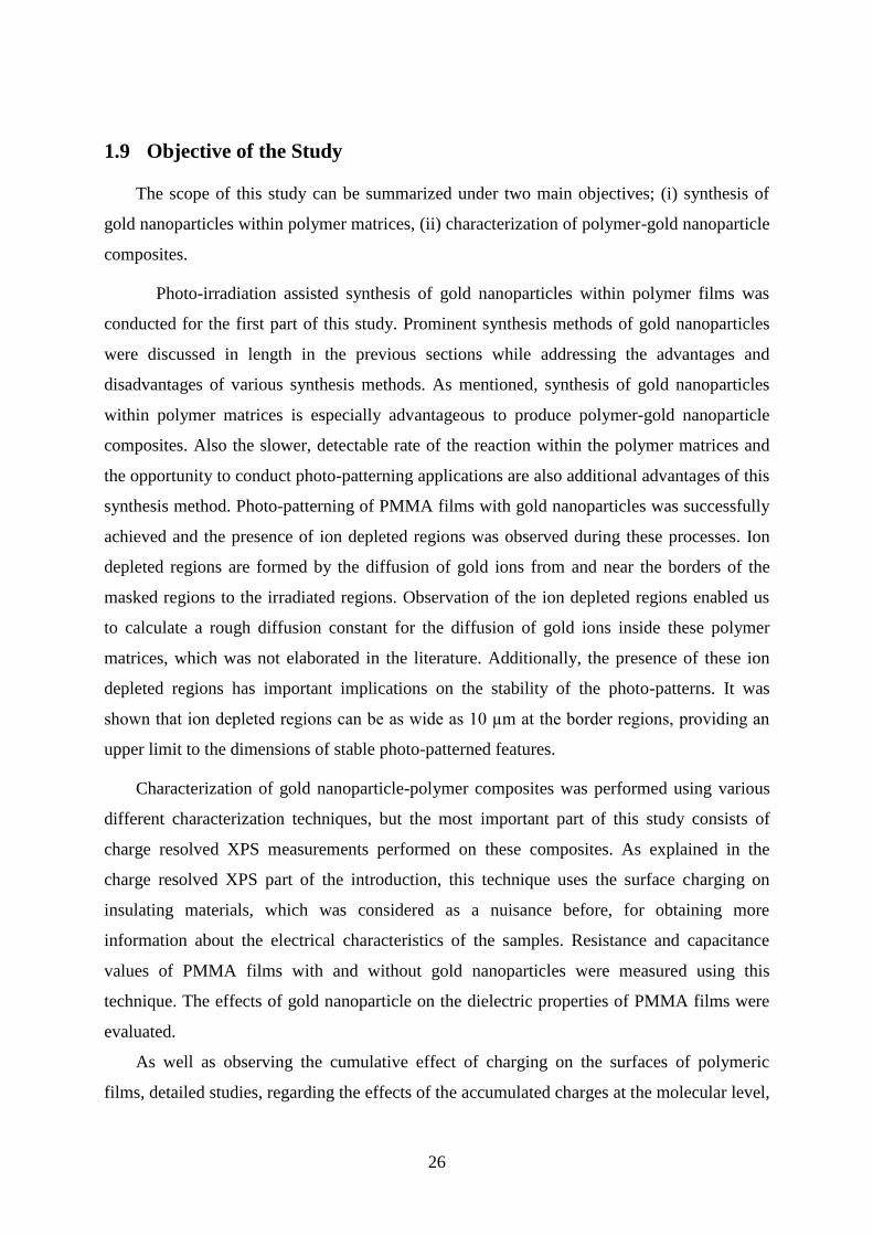
26
1.9 Objective of the Study
The scope of this study can be summarized under two main objectives; (i) synthesis of
gold nanoparticles within polymer matrices, (ii) characterization of polymer-gold nanoparticle
composites.
Photo-irradiation assisted synthesis of gold nanoparticles within polymer films was
conducted for the first part of this study. Prominent synthesis methods of gold nanoparticles
were discussed in length in the previous sections while addressing the advantages and
disadvantages of various synthesis methods. As mentioned, synthesis of gold nanoparticles
within polymer matrices is especially advantageous to produce polymer-gold nanoparticle
composites. Also the slower, detectable rate of the reaction within the polymer matrices and
the opportunity to conduct photo-patterning applications are also additional advantages of this
synthesis method. Photo-patterning of PMMA films with gold nanoparticles was successfully
achieved and the presence of ion depleted regions was observed during these processes. Ion
depleted regions are formed by the diffusion of gold ions from and near the borders of the
masked regions to the irradiated regions. Observation of the ion depleted regions enabled us
to calculate a rough diffusion constant for the diffusion of gold ions inside these polymer
matrices, which was not elaborated in the literature. Additionally, the presence of these ion
depleted regions has important implications on the stability of the photo-patterns. It was
shown that ion depleted regions can be as wide as 10 µm at the border regions, providing an
upper limit to the dimensions of stable photo-patterned features.
Characterization of gold nanoparticle-polymer composites was performed using various
different characterization techniques, but the most important part of this study consists of
charge resolved XPS measurements performed on these composites. As explained in the
charge resolved XPS part of the introduction, this technique uses the surface charging on
insulating materials, which was considered as a nuisance before, for obtaining more
information about the electrical characteristics of the samples. Resistance and capacitance
values of PMMA films with and without gold nanoparticles were measured using this
technique. The effects of gold nanoparticle on the dielectric properties of PMMA films were
evaluated.
As well as observing the cumulative effect of charging on the surfaces of polymeric
films, detailed studies, regarding the effects of the accumulated charges at the molecular level,
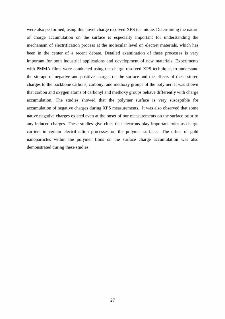
27
were also performed, using this novel charge resolved XPS technique. Determining the nature
of charge accumulation on the surface is especially important for understanding the
mechanism of electrification process at the molecular level on electret materials, which has
been in the center of a recent debate. Detailed examination of these processes is very
important for both industrial applications and development of new materials. Experiments
with PMMA films were conducted using the charge resolved XPS technique, to understand
the storage of negative and positive charges on the surface and the effects of these stored
charges to the backbone carbons, carbonyl and methoxy groups of the polymer. It was shown
that carbon and oxygen atoms of carbonyl and methoxy groups behave differently with charge
accumulation. The studies showed that the polymer surface is very susceptible for
accumulation of negative charges during XPS measurements. It was also observed that some
native negative charges existed even at the onset of our measurements on the surface prior to
any induced charges. These studies give clues that electrons play important roles as charge
carriers in certain electrification processes on the polymer surfaces. The effect of gold
nanoparticles within the polymer films on the surface charge accumulation was also
demonstrated during these studies.
28
2 Experimental
2.1 Materials
Poly(methyl methacrylate) (PMMA), poly(vinyl alcohol) (PVA), Hydrogen
tetrachloroaurate (HAuCl4), Silver nitrate (AgNO3), benzophenone and rhodamine 6G were
purchased from Aldrich and used without further purification. Absolute acetone with a purity
>99.5% was used for the preparation of all samples. Deionized water was used for the
cleaning and sample preparation purposes.
2.2 Preparation of Samples
PMMA films containing gold ions were prepared by firstly dissolving both HAuCl4
and PMMA in an appropriate common solvent, which was acetone for most of the
experiments. Then the solutions of both reagents were mixed in various ratios to prepare the
mixture to cast the films. HAuCl4 solution concentration can vary from 10-2
M to 10-4
M
depending on the experiment type and PMMA solution concentration can vary in between
0.5% and 10% (w/w) depending on the required film thickness.
Thickness of the prepared films depends on a couple of factors. Firstly, the
concentration of the polymer solution is important. Thick films can be produced using higher
concentrations of PMMA solution. The second factor affecting the film thickness is the
preparation method. Uniform films of PMMA can be prepared either with spin-coating, or
room temperature casting in which the polymer solution is casted on a flat surface and the
solvent is evaporated at room temperature slowly. In our studies thick films were produced
from ~5-10% (w/w) solutions by room temperature casting on flat surfaces (glass or
polypropylene substrates), the fully dried films then can be extracted as free standing polymer
films. During evaporation process an acetone rich atmosphere around the sample may be
necessary for obtaining clear films. On the other hand, thin films was prepared in the range of
tens to hundreds of nanometers thicknesses by the spin coating technique, which is
schematically described in Figure 2.1. During spin coating process, excess amount of the
solution for the targeted film is dropped on the substrate surface while the substrate spins at
full speed and homogeneous films can be produced with the aid of centrifugal force. For spin
coated PMMA films, ~0.5-2% (w/w, depending on the desired thickness) PMMA solution is
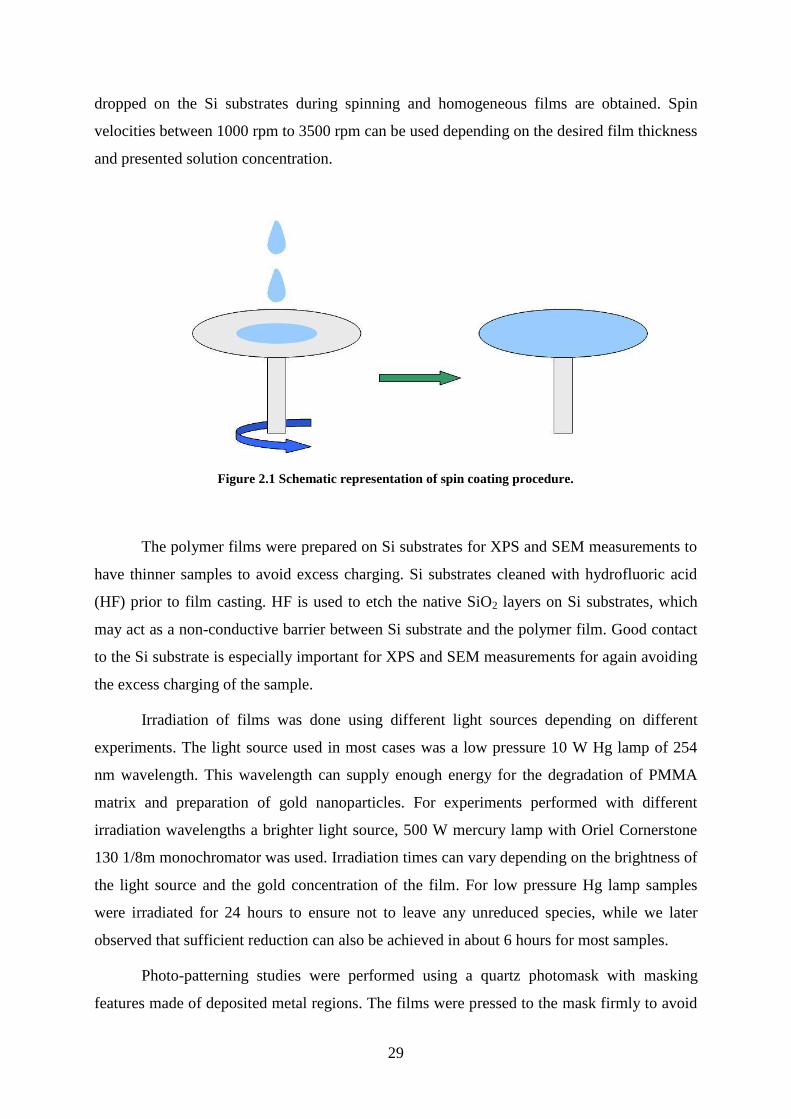
29
dropped on the Si substrates during spinning and homogeneous films are obtained. Spin
velocities between 1000 rpm to 3500 rpm can be used depending on the desired film thickness
and presented solution concentration.
Figure 2.1 Schematic representation of spin coating procedure.
The polymer films were prepared on Si substrates for XPS and SEM measurements to
have thinner samples to avoid excess charging. Si substrates cleaned with hydrofluoric acid
(HF) prior to film casting. HF is used to etch the native SiO2 layers on Si substrates, which
may act as a non-conductive barrier between Si substrate and the polymer film. Good contact
to the Si substrate is especially important for XPS and SEM measurements for again avoiding
the excess charging of the sample.
Irradiation of films was done using different light sources depending on different
experiments. The light source used in most cases was a low pressure 10 W Hg lamp of 254
nm wavelength. This wavelength can supply enough energy for the degradation of PMMA
matrix and preparation of gold nanoparticles. For experiments performed with different
irradiation wavelengths a brighter light source, 500 W mercury lamp with Oriel Cornerstone
130 1/8m monochromator was used. Irradiation times can vary depending on the brightness of
the light source and the gold concentration of the film. For low pressure Hg lamp samples
were irradiated for 24 hours to ensure not to leave any unreduced species, while we later
observed that sufficient reduction can also be achieved in about 6 hours for most samples.
Photo-patterning studies were performed using a quartz photomask with masking
features made of deposited metal regions. The films were pressed to the mask firmly to avoid
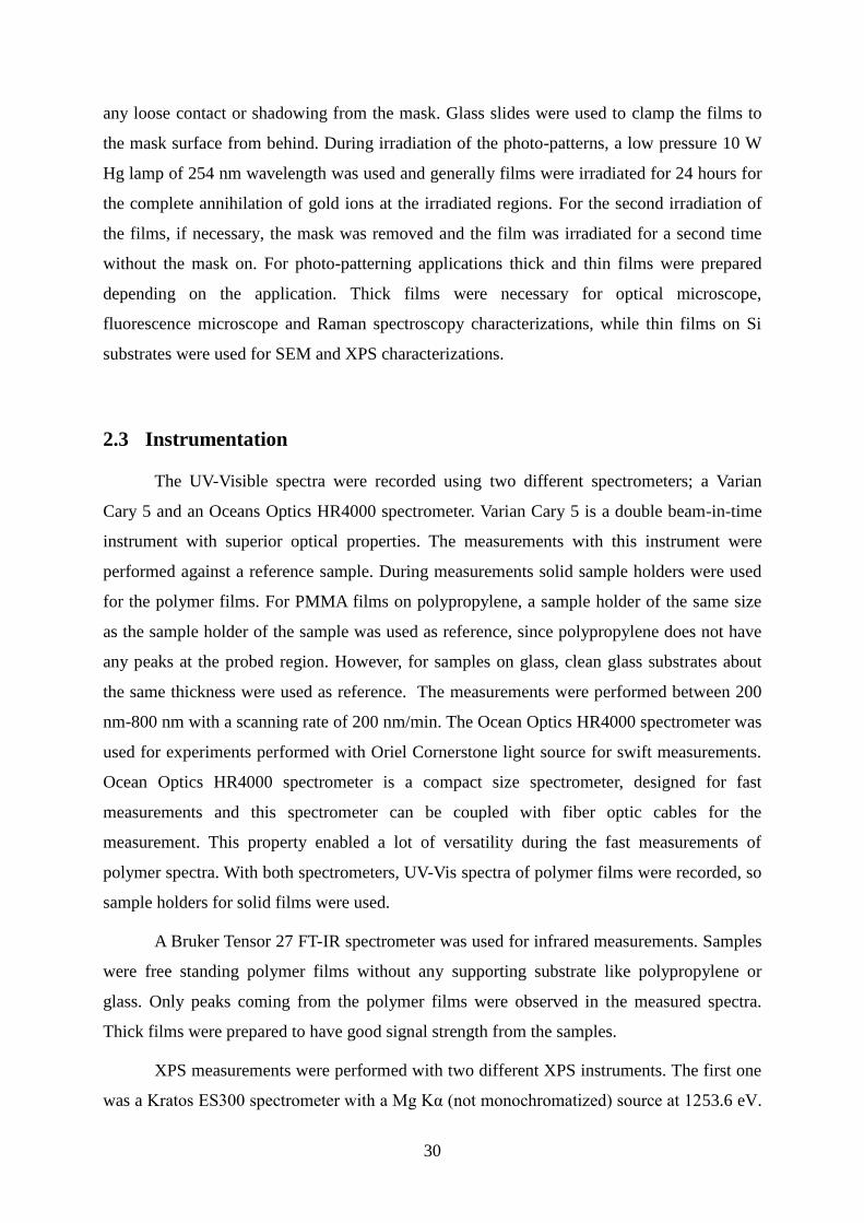
30
any loose contact or shadowing from the mask. Glass slides were used to clamp the films to
the mask surface from behind. During irradiation of the photo-patterns, a low pressure 10 W
Hg lamp of 254 nm wavelength was used and generally films were irradiated for 24 hours for
the complete annihilation of gold ions at the irradiated regions. For the second irradiation of
the films, if necessary, the mask was removed and the film was irradiated for a second time
without the mask on. For photo-patterning applications thick and thin films were prepared
depending on the application. Thick films were necessary for optical microscope,
fluorescence microscope and Raman spectroscopy characterizations, while thin films on Si
substrates were used for SEM and XPS characterizations.
2.3 Instrumentation
The UV-Visible spectra were recorded using two different spectrometers; a Varian
Cary 5 and an Oceans Optics HR4000 spectrometer. Varian Cary 5 is a double beam-in-time
instrument with superior optical properties. The measurements with this instrument were
performed against a reference sample. During measurements solid sample holders were used
for the polymer films. For PMMA films on polypropylene, a sample holder of the same size
as the sample holder of the sample was used as reference, since polypropylene does not have
any peaks at the probed region. However, for samples on glass, clean glass substrates about
the same thickness were used as reference. The measurements were performed between 200
nm-800 nm with a scanning rate of 200 nm/min. The Ocean Optics HR4000 spectrometer was
used for experiments performed with Oriel Cornerstone light source for swift measurements.
Ocean Optics HR4000 spectrometer is a compact size spectrometer, designed for fast
measurements and this spectrometer can be coupled with fiber optic cables for the
measurement. This property enabled a lot of versatility during the fast measurements of
polymer spectra. With both spectrometers, UV-Vis spectra of polymer films were recorded, so
sample holders for solid films were used.
A Bruker Tensor 27 FT-IR spectrometer was used for infrared measurements. Samples
were free standing polymer films without any supporting substrate like polypropylene or
glass. Only peaks coming from the polymer films were observed in the measured spectra.
Thick films were prepared to have good signal strength from the samples.
XPS measurements were performed with two different XPS instruments. The first one
was a Kratos ES300 spectrometer with a Mg Kα (not monochromatized) source at 1253.6 eV.
31
This instrument analyzes the signal coming from nearly all the sample surface instead of
focusing to one spot, so the spectra taken with this instrument are always an average of the
signal from the sample. Charging experiments on PMMA films with and without gold
nanoparticles were performed using this instrument while applying DC bias or square wave
pulses of +/-10 V to the sample holder. An electron filament was used in some measurements
for the neutralization of the sample surface against excess charging.
The second instrument used for the XPS measurements was a Thermo Sceintific K-
Alpha XPS spectrometer with a monochromatized source with 1486.68 eV photon energy.
This spectrometer can probe the sample with a small x-ray spot size between 30 µm-400 µm.
And it‟s equipped with a flood gun as an external electron and ion source for the
neutralization of the sample surface when necessary. Using this instrument charge resolved
XPS measurements can be performed with DC bias or SQW pulses and as well as other
measurements like line scan or area scan on the sample. One advantage of this instrument was
collecting snapshot spectra of the sample very fast and being able to monitor the movement in
peak positions in very small time intervals. Snapshot spectra mode was used especially with
charge resolved XPS technique using SQW pulses to monitor the changes in the sample
during the charging events. A schematic representation of charge resolved XPS measurements
with SQW pulses monitored with snapshot mode and its interpretation is given in Figure 2.2.
As can be seen in the figure, the spectra of the relevant lines were collected step by step with
this technique very swiftly (0.01 – 1.0 sec for each spectrum depending on the experiment
conditions) and as a result the collection of these spectra clearly shows the movement of the
line during biasing. Then those spectra can be fitted and the line positions can be calculated
and plotted for the quantification of the charging event.
32
Figure 2.2 Illustration of experimental setup for the SQW voltage applied measurement on PMMA films.
The XPS spectra data obtained were fitted using the XPSPEAK 4.0 fitting program for
individual spectra and automatically fitted by Avantage program for the snapshot
experiments. Then those data were plotted using Origin 7.5. The data were normally recorded
at a 90° electron takeoff angle.
Scanning electron microscope images were taken by a Zeiss EVO 40 electron
microscope. This instrument can provide electron beam brightness up to 30 kV, but our
measurements were generally performed at beam energies between 5 kV to 10 kV since
polymer films can easily burn at high energy electron beams. Both secondary electron
detector and backscattered electron detector were available and measurements with both of
them were performed. SEM was especially used for the imaging of photo-patterns in this
study. Regions containing gold nanoparticles of the photo-patterns appeared brighter than the
other regions because of the high secondary electron yield of gold nanoparticles. This
instrument was also equipped with an energy dispersive x-ray detector, which can analyze the
33
x-rays emitted from the sample along with the secondary electrons for chemical
characterization of the sample. We also tried to use this technique for the characterization of
our patterned films, but we couldn‟t obtain consistent results because of the low energy of the
beam. For good results in energy dispersive x-ray technique high beam voltages should be
employed, which in our case results the burning of the polymer films.
Zeiss Axio Imager A1 was used for our fluorescence microscope imaging. Our
samples contained Rhodamine 6G dye molecules, which emits fluorescence strongly between
500 nm and 700 nm when excited with 480 nm light. This microscope is a polarized light
microscope which was originally designed for the fluorescence studies in biological systems.
By our trials we also found out that FITC filter, which excites at around 490 nm and collects
around 520 nm, was the most efficient filter for our samples.
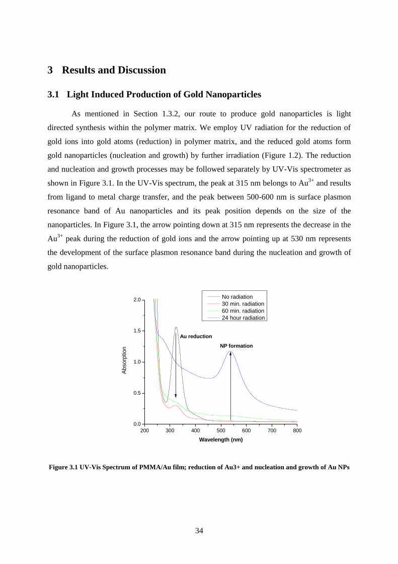
34
3 Results and Discussion
3.1 Light Induced Production of Gold Nanoparticles
As mentioned in Section 1.3.2, our route to produce gold nanoparticles is light
directed synthesis within the polymer matrix. We employ UV radiation for the reduction of
gold ions into gold atoms (reduction) in polymer matrix, and the reduced gold atoms form
gold nanoparticles (nucleation and growth) by further irradiation (Figure 1.2). The reduction
and nucleation and growth processes may be followed separately by UV-Vis spectrometer as
shown in Figure 3.1. In the UV-Vis spectrum, the peak at 315 nm belongs to Au3+
and results
from ligand to metal charge transfer, and the peak between 500-600 nm is surface plasmon
resonance band of Au nanoparticles and its peak position depends on the size of the
nanoparticles. In Figure 3.1, the arrow pointing down at 315 nm represents the decrease in the
Au3+
peak during the reduction of gold ions and the arrow pointing up at 530 nm represents
the development of the surface plasmon resonance band during the nucleation and growth of
gold nanoparticles.
Figure 3.1 UV-Vis Spectrum of PMMA/Au film; reduction of Au3+ and nucleation and growth of Au NPs
200 300 400 500 600 700 800
0.0
0.5
1.0
1.5
2.0
Ab
so
rptio
n
Wavelength (nm)
No radiation
30 min. radiation
60 min. radiation
24 hour radiation
NP formation
Au reduction
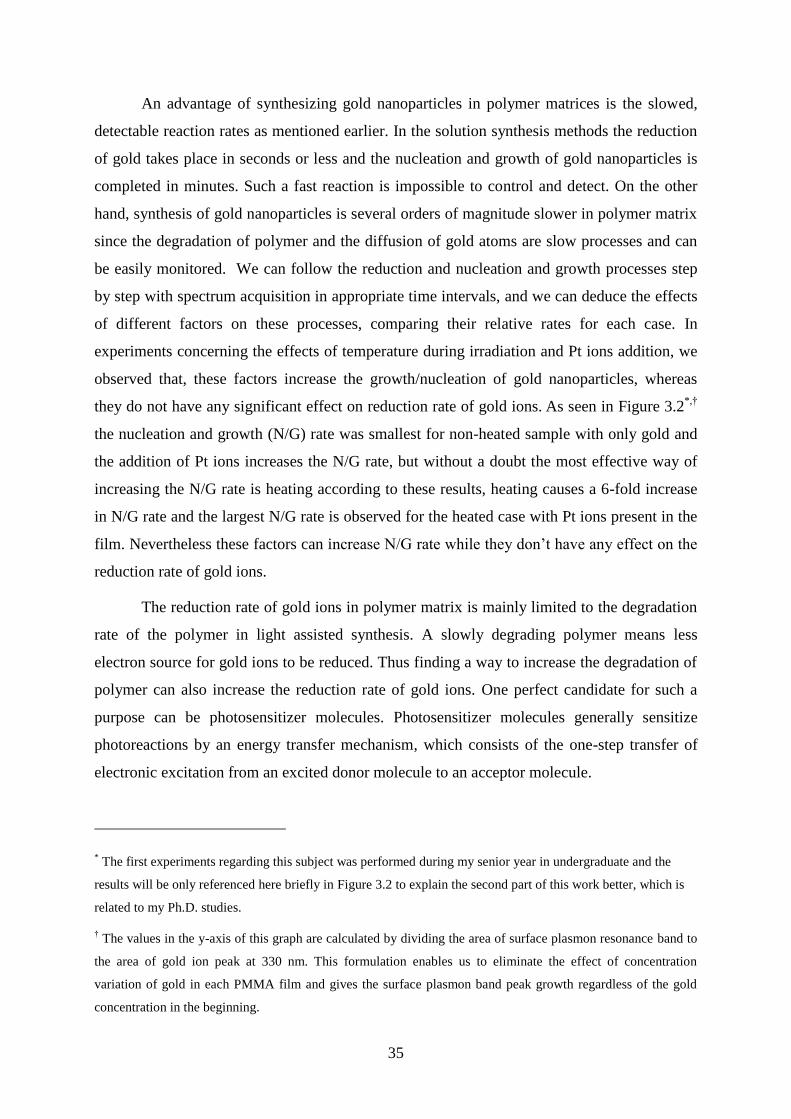
35
An advantage of synthesizing gold nanoparticles in polymer matrices is the slowed,
detectable reaction rates as mentioned earlier. In the solution synthesis methods the reduction
of gold takes place in seconds or less and the nucleation and growth of gold nanoparticles is
completed in minutes. Such a fast reaction is impossible to control and detect. On the other
hand, synthesis of gold nanoparticles is several orders of magnitude slower in polymer matrix
since the degradation of polymer and the diffusion of gold atoms are slow processes and can
be easily monitored. We can follow the reduction and nucleation and growth processes step
by step with spectrum acquisition in appropriate time intervals, and we can deduce the effects
of different factors on these processes, comparing their relative rates for each case. In
experiments concerning the effects of temperature during irradiation and Pt ions addition, we
observed that, these factors increase the growth/nucleation of gold nanoparticles, whereas
they do not have any significant effect on reduction rate of gold ions. As seen in Figure 3.2
*,†
the nucleation and growth (N/G) rate was smallest for non-heated sample with only gold and
the addition of Pt ions increases the N/G rate, but without a doubt the most effective way of
increasing the N/G rate is heating according to these results, heating causes a 6-fold increase
in N/G rate and the largest N/G rate is observed for the heated case with Pt ions present in the
film. Nevertheless these factors can increase N/G rate while they don‟t have any effect on the
reduction rate of gold ions.
The reduction rate of gold ions in polymer matrix is mainly limited to the degradation
rate of the polymer in light assisted synthesis. A slowly degrading polymer means less
electron source for gold ions to be reduced. Thus finding a way to increase the degradation of
polymer can also increase the reduction rate of gold ions. One perfect candidate for such a
purpose can be photosensitizer molecules. Photosensitizer molecules generally sensitize
photoreactions by an energy transfer mechanism, which consists of the one-step transfer of
electronic excitation from an excited donor molecule to an acceptor molecule.
* The first experiments regarding this subject was performed during my senior year in undergraduate and the
results will be only referenced here briefly in Figure 3.2 to explain the second part of this work better, which is
related to my Ph.D. studies.
† The values in the y-axis of this graph are calculated by dividing the area of surface plasmon resonance band to
the area of gold ion peak at 330 nm. This formulation enables us to eliminate the effect of concentration
variation of gold in each PMMA film and gives the surface plasmon band peak growth regardless of the gold
concentration in the beginning.
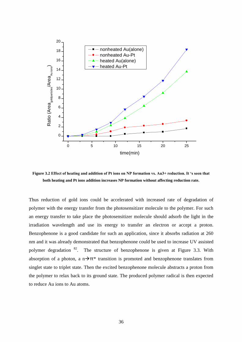
36
Figure 3.2 Effect of heating and addition of Pt ions on NP formation vs. Au3+ reduction. It ‘s seen that
both heating and Pt ions addition increases NP formation without affecting reduction rate.
Thus reduction of gold ions could be accelerated with increased rate of degradation of
polymer with the energy transfer from the photosensitizer molecule to the polymer. For such
an energy transfer to take place the photosensitizer molecule should adsorb the light in the
irradiation wavelength and use its energy to transfer an electron or accept a proton.
Benzophenone is a good candidate for such an application, since it absorbs radiation at 260
nm and it was already demonstrated that benzophenone could be used to increase UV assisted
polymer degradation 82
. The structure of benzophenone is given at Figure 3.3. With
absorption of a photon, a nπ* transition is promoted and benzophenone translates from
singlet state to triplet state. Then the excited benzophenone molecule abstracts a proton from
the polymer to relax back to its ground state. The produced polymer radical is then expected
to reduce Au ions to Au atoms.
0 5 10 15 20 25
0
2
4
6
8
10
12
14
16
18
20
Ra
tio
(A
rea
gold
part
icle
s/A
rea
Au ions)
time(min)
nonheated Au(alone)
nonheated Au-Pt
heated Au(alone)
heated Au-Pt
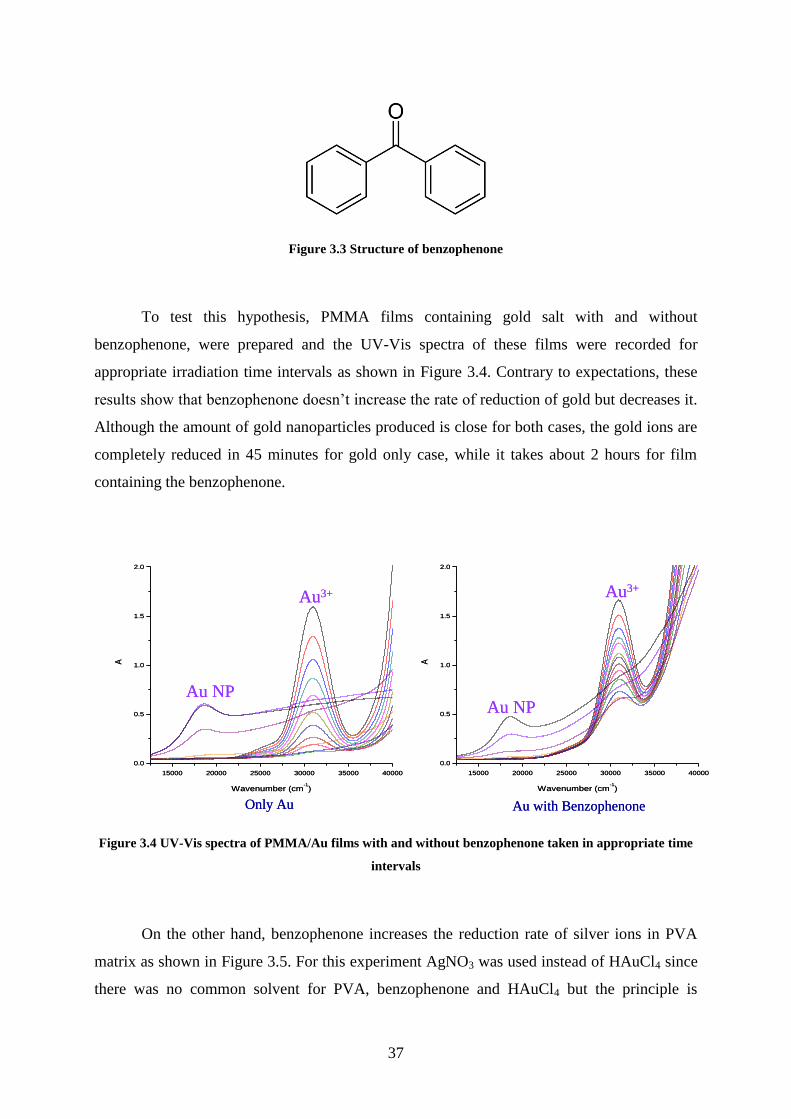
37
Figure 3.3 Structure of benzophenone
To test this hypothesis, PMMA films containing gold salt with and without
benzophenone, were prepared and the UV-Vis spectra of these films were recorded for
appropriate irradiation time intervals as shown in Figure 3.4. Contrary to expectations, these
results show that benzophenone doesn‟t increase the rate of reduction of gold but decreases it.
Although the amount of gold nanoparticles produced is close for both cases, the gold ions are
completely reduced in 45 minutes for gold only case, while it takes about 2 hours for film
containing the benzophenone.
Figure 3.4 UV-Vis spectra of PMMA/Au films with and without benzophenone taken in appropriate time
intervals
On the other hand, benzophenone increases the reduction rate of silver ions in PVA
matrix as shown in Figure 3.5. For this experiment AgNO3 was used instead of HAuCl4 since
there was no common solvent for PVA, benzophenone and HAuCl4 but the principle is
15000 20000 25000 30000 35000 40000
0.0
0.5
1.0
1.5
2.0
A
Wavenumber (cm-1)
15000 20000 25000 30000 35000 40000
0.0
0.5
1.0
1.5
2.0
A
Wavenumber (cm-1)
Only Au Au with Benzophenone
Au NPAu NP
Au3+ Au3+
15000 20000 25000 30000 35000 40000
0.0
0.5
1.0
1.5
2.0
A
Wavenumber (cm-1)
15000 20000 25000 30000 35000 40000
0.0
0.5
1.0
1.5
2.0
A
Wavenumber (cm-1)
Only Au Au with Benzophenone
Au NPAu NP
Au3+ Au3+
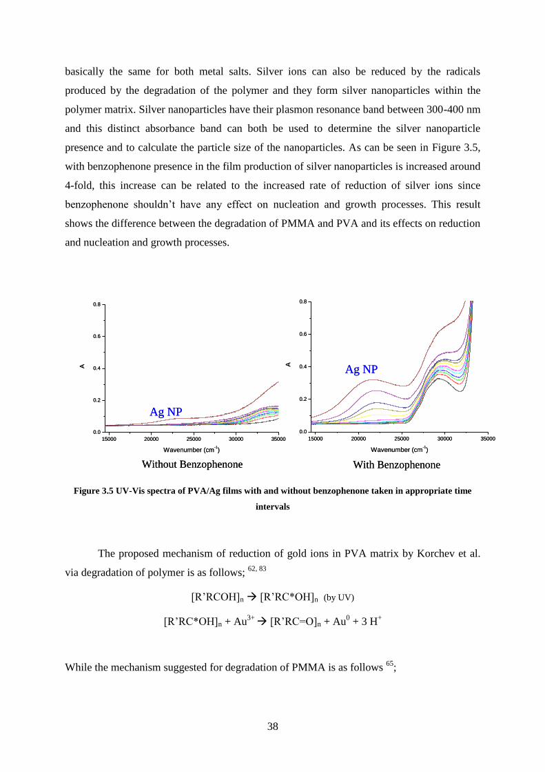
38
basically the same for both metal salts. Silver ions can also be reduced by the radicals
produced by the degradation of the polymer and they form silver nanoparticles within the
polymer matrix. Silver nanoparticles have their plasmon resonance band between 300-400 nm
and this distinct absorbance band can both be used to determine the silver nanoparticle
presence and to calculate the particle size of the nanoparticles. As can be seen in Figure 3.5,
with benzophenone presence in the film production of silver nanoparticles is increased around
4-fold, this increase can be related to the increased rate of reduction of silver ions since
benzophenone shouldn‟t have any effect on nucleation and growth processes. This result
shows the difference between the degradation of PMMA and PVA and its effects on reduction
and nucleation and growth processes.
Figure 3.5 UV-Vis spectra of PVA/Ag films with and without benzophenone taken in appropriate time
intervals
The proposed mechanism of reduction of gold ions in PVA matrix by Korchev et al.
via degradation of polymer is as follows; 62, 83
[R‟RCOH]n [R‟RC*OH]n (by UV)
[R‟RC*OH]n + Au3+ [R‟RC=O]n + Au
0 + 3 H
+
While the mechanism suggested for degradation of PMMA is as follows 65
;
15000 20000 25000 30000 35000
0.0
0.2
0.4
0.6
0.8
A
Wavenumber (cm-1)
15000 20000 25000 30000 35000
0.0
0.2
0.4
0.6
0.8
A
Wavenumber (cm-1)
Without Benzophenone With Benzophenone
Ag NP
Ag NP
15000 20000 25000 30000 35000
0.0
0.2
0.4
0.6
0.8
A
Wavenumber (cm-1)
15000 20000 25000 30000 35000
0.0
0.2
0.4
0.6
0.8
A
Wavenumber (cm-1)
Without Benzophenone With Benzophenone
Ag NP
Ag NP
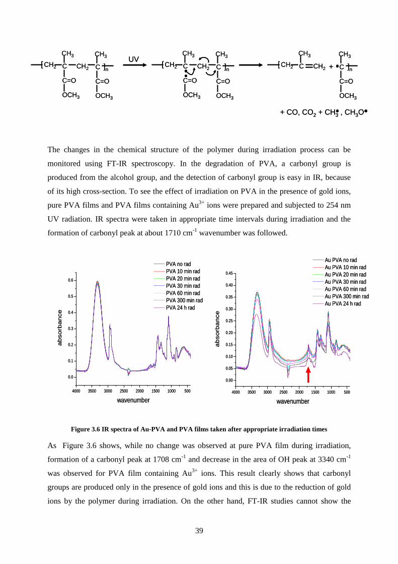
39
The changes in the chemical structure of the polymer during irradiation process can be
monitored using FT-IR spectroscopy. In the degradation of PVA, a carbonyl group is
produced from the alcohol group, and the detection of carbonyl group is easy in IR, because
of its high cross-section. To see the effect of irradiation on PVA in the presence of gold ions,
pure PVA films and PVA films containing Au3+
ions were prepared and subjected to 254 nm
UV radiation. IR spectra were taken in appropriate time intervals during irradiation and the
formation of carbonyl peak at about 1710 cm-1
wavenumber was followed.
Figure 3.6 IR spectra of Au-PVA and PVA films taken after appropriate irradiation times
As Figure 3.6 shows, while no change was observed at pure PVA film during irradiation,
formation of a carbonyl peak at 1708 cm-1
and decrease in the area of OH peak at 3340 cm-1
was observed for PVA film containing Au3+
ions. This result clearly shows that carbonyl
groups are produced only in the presence of gold ions and this is due to the reduction of gold
ions by the polymer during irradiation. On the other hand, FT-IR studies cannot show the
CH3
CH2 C
C=O
OCH3
CH2
CH3
C
OCH3
C=O
[ ]n
UVCH3
CH2 C
C=O
OCH3
CH2
CH3
C
OCH3
C=O
[ ]n
CH3
CH2 C CH2
CH3
C
OCH3
C=O
[ ]n+
+ CO, CO2 + CH3 , CH3O
CH3
CH2 C
C=O
OCH3
CH2
CH3
C
OCH3
C=O
[ ]n
UVCH3
CH2 C
C=O
OCH3
CH2
CH3
C
OCH3
C=O
[ ]n
CH3
CH2 C CH2
CH3
C
OCH3
C=O
[ ]n+
+ CO, CO2 + CH3 , CH3O
4000 3500 3000 2500 2000 1500 1000 500
0.0
0.1
0.2
0.3
0.4
0.5
0.6
PVA no rad
PVA 10 min rad
PVA 20 min rad
PVA 30 min rad
PVA 60 min rad
PVA 300 min rad
PVA 24 h rad
ab
so
rba
nce
wavenumber
4000 3500 3000 2500 2000 1500 1000 500
0.00
0.05
0.10
0.15
0.20
0.25
0.30
0.35
0.40
0.45
Au PVA no rad
Au PVA 10 min rad
Au PVA 20 min rad
Au PVA 30 min rad
Au PVA 60 min rad
Au PVA 300 min rad
Au PVA 24 h rad
ab
so
rba
nce
wavenumber
4000 3500 3000 2500 2000 1500 1000 500
0.0
0.1
0.2
0.3
0.4
0.5
0.6
PVA no rad
PVA 10 min rad
PVA 20 min rad
PVA 30 min rad
PVA 60 min rad
PVA 300 min rad
PVA 24 h rad
ab
so
rba
nce
wavenumber
4000 3500 3000 2500 2000 1500 1000 500
0.00
0.05
0.10
0.15
0.20
0.25
0.30
0.35
0.40
0.45
Au PVA no rad
Au PVA 10 min rad
Au PVA 20 min rad
Au PVA 30 min rad
Au PVA 60 min rad
Au PVA 300 min rad
Au PVA 24 h rad
ab
so
rba
nce
wavenumber
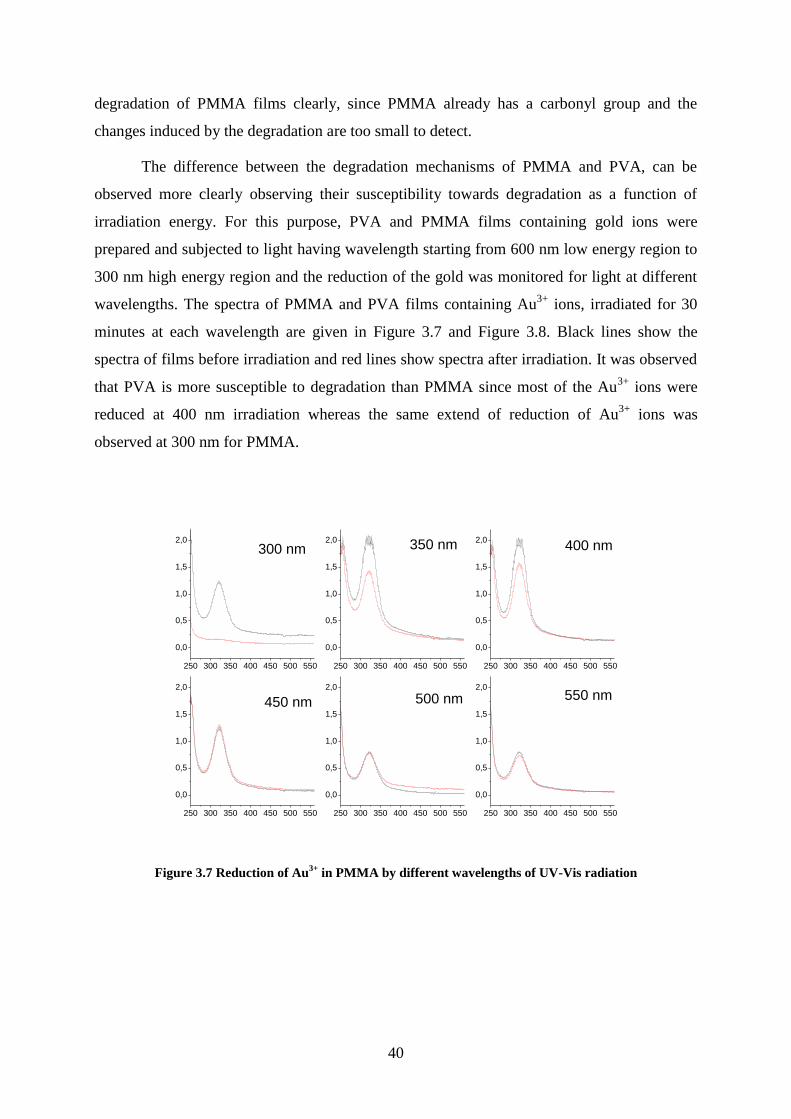
40
degradation of PMMA films clearly, since PMMA already has a carbonyl group and the
changes induced by the degradation are too small to detect.
The difference between the degradation mechanisms of PMMA and PVA, can be
observed more clearly observing their susceptibility towards degradation as a function of
irradiation energy. For this purpose, PVA and PMMA films containing gold ions were
prepared and subjected to light having wavelength starting from 600 nm low energy region to
300 nm high energy region and the reduction of the gold was monitored for light at different
wavelengths. The spectra of PMMA and PVA films containing Au3+
ions, irradiated for 30
minutes at each wavelength are given in Figure 3.7 and Figure 3.8. Black lines show the
spectra of films before irradiation and red lines show spectra after irradiation. It was observed
that PVA is more susceptible to degradation than PMMA since most of the Au3+
ions were
reduced at 400 nm irradiation whereas the same extend of reduction of Au3+
ions was
observed at 300 nm for PMMA.
250 300 350 400 450 500 550
0,0
0,5
1,0
1,5
2,0
300 nm
250 300 350 400 450 500 550
0,0
0,5
1,0
1,5
2,0 350 nm
250 300 350 400 450 500 550
0,0
0,5
1,0
1,5
2,0400 nm
250 300 350 400 450 500 550
0,0
0,5
1,0
1,5
2,0
450 nm
250 300 350 400 450 500 550
0,0
0,5
1,0
1,5
2,0
500 nm
250 300 350 400 450 500 550
0,0
0,5
1,0
1,5
2,0
550 nm
Figure 3.7 Reduction of Au3+
in PMMA by different wavelengths of UV-Vis radiation
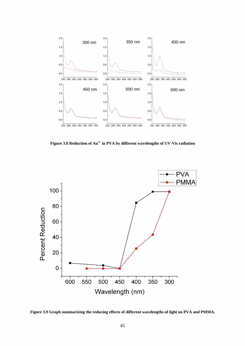
41
250 300 350 400 450 500 550
0,0
0,5
1,0
1,5
2,0
300 nm
250 300 350 400 450 500 550
0,0
0,5
1,0
1,5
2,0
350 nm
250 300 350 400 450 500 550
0,0
0,5
1,0
1,5
2,0
400 nm
250 300 350 400 450 500 550
0,0
0,5
1,0
1,5
2,0
450 nm
250 300 350 400 450 500 550
0,0
0,5
1,0
1,5
2,0
500 nm
250 300 350 400 450 500 550
0,0
0,5
1,0
1,5
2,0
600 nm
Figure 3.8 Reduction of Au3+
in PVA by different wavelengths of UV-Vis radiation
Figure 3.9 Graph summarizing the reducing effects of different wavelengths of light on PVA and PMMA.
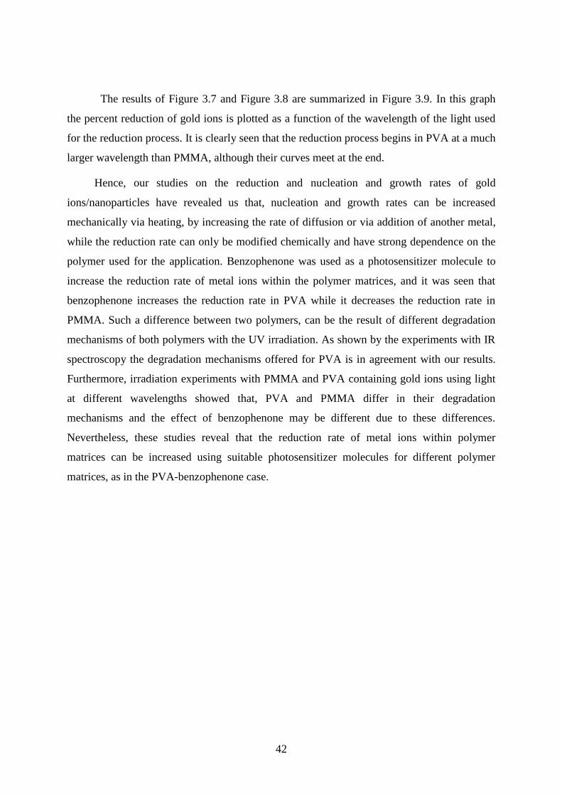
42
The results of Figure 3.7 and Figure 3.8 are summarized in Figure 3.9. In this graph
the percent reduction of gold ions is plotted as a function of the wavelength of the light used
for the reduction process. It is clearly seen that the reduction process begins in PVA at a much
larger wavelength than PMMA, although their curves meet at the end.
Hence, our studies on the reduction and nucleation and growth rates of gold
ions/nanoparticles have revealed us that, nucleation and growth rates can be increased
mechanically via heating, by increasing the rate of diffusion or via addition of another metal,
while the reduction rate can only be modified chemically and have strong dependence on the
polymer used for the application. Benzophenone was used as a photosensitizer molecule to
increase the reduction rate of metal ions within the polymer matrices, and it was seen that
benzophenone increases the reduction rate in PVA while it decreases the reduction rate in
PMMA. Such a difference between two polymers, can be the result of different degradation
mechanisms of both polymers with the UV irradiation. As shown by the experiments with IR
spectroscopy the degradation mechanisms offered for PVA is in agreement with our results.
Furthermore, irradiation experiments with PMMA and PVA containing gold ions using light
at different wavelengths showed that, PVA and PMMA differ in their degradation
mechanisms and the effect of benzophenone may be different due to these differences.
Nevertheless, these studies reveal that the reduction rate of metal ions within polymer
matrices can be increased using suitable photosensitizer molecules for different polymer
matrices, as in the PVA-benzophenone case.
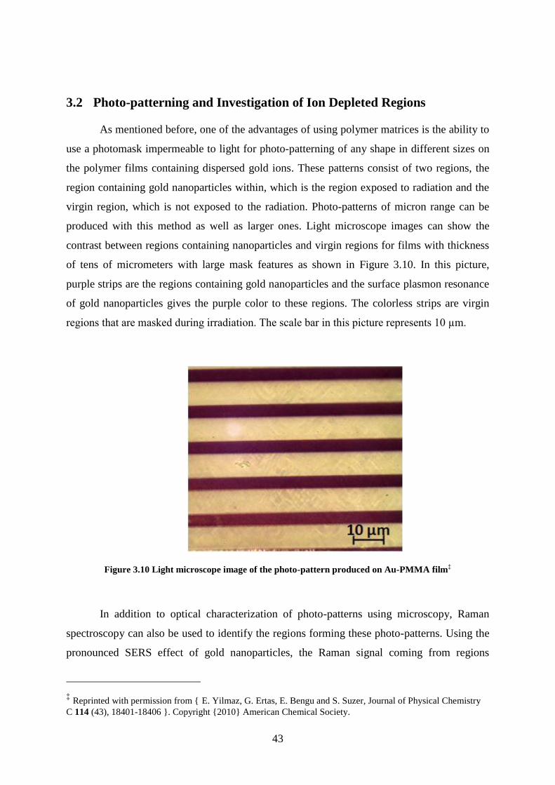
43
3.2 Photo-patterning and Investigation of Ion Depleted Regions
As mentioned before, one of the advantages of using polymer matrices is the ability to
use a photomask impermeable to light for photo-patterning of any shape in different sizes on
the polymer films containing dispersed gold ions. These patterns consist of two regions, the
region containing gold nanoparticles within, which is the region exposed to radiation and the
virgin region, which is not exposed to the radiation. Photo-patterns of micron range can be
produced with this method as well as larger ones. Light microscope images can show the
contrast between regions containing nanoparticles and virgin regions for films with thickness
of tens of micrometers with large mask features as shown in Figure 3.10. In this picture,
purple strips are the regions containing gold nanoparticles and the surface plasmon resonance
of gold nanoparticles gives the purple color to these regions. The colorless strips are virgin
regions that are masked during irradiation. The scale bar in this picture represents 10 µm.
Figure 3.10 Light microscope image of the photo-pattern produced on Au-PMMA film‡
In addition to optical characterization of photo-patterns using microscopy, Raman
spectroscopy can also be used to identify the regions forming these photo-patterns. Using the
pronounced SERS effect of gold nanoparticles, the Raman signal coming from regions
‡ Reprinted with permission from { E. Yilmaz, G. Ertas, E. Bengu and S. Suzer, Journal of Physical Chemistry
C 114 (43), 18401-18406 }. Copyright {2010} American Chemical Society.
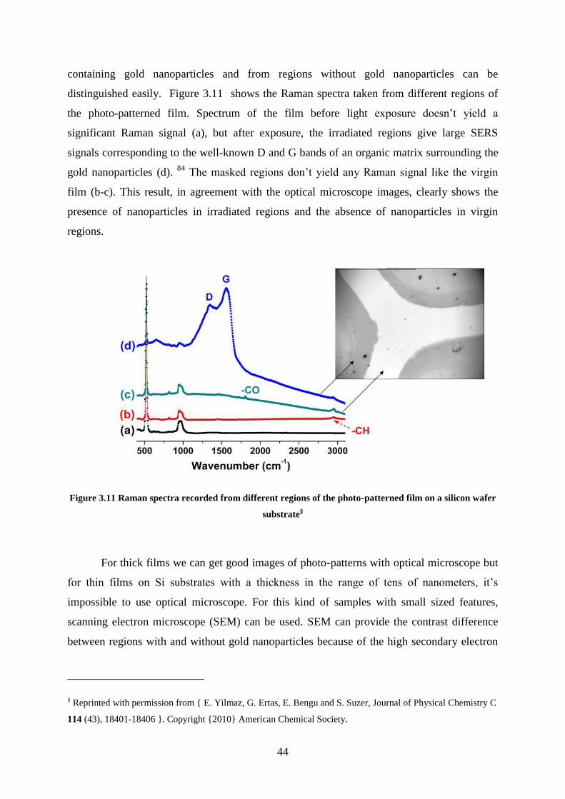
44
containing gold nanoparticles and from regions without gold nanoparticles can be
distinguished easily. Figure 3.11 shows the Raman spectra taken from different regions of
the photo-patterned film. Spectrum of the film before light exposure doesn‟t yield a
significant Raman signal (a), but after exposure, the irradiated regions give large SERS
signals corresponding to the well-known D and G bands of an organic matrix surrounding the
gold nanoparticles (d). 84
The masked regions don‟t yield any Raman signal like the virgin
film (b-c). This result, in agreement with the optical microscope images, clearly shows the
presence of nanoparticles in irradiated regions and the absence of nanoparticles in virgin
regions.
Figure 3.11 Raman spectra recorded from different regions of the photo-patterned film on a silicon wafer
substrate§
For thick films we can get good images of photo-patterns with optical microscope but
for thin films on Si substrates with a thickness in the range of tens of nanometers, it‟s
impossible to use optical microscope. For this kind of samples with small sized features,
scanning electron microscope (SEM) can be used. SEM can provide the contrast difference
between regions with and without gold nanoparticles because of the high secondary electron
§ Reprinted with permission from { E. Yilmaz, G. Ertas, E. Bengu and S. Suzer, Journal of Physical Chemistry C
114 (43), 18401-18406 }. Copyright {2010} American Chemical Society.
45
yield of gold atoms or ions. Also with the use of backscattered electron detector in SEM, the
regions containing high Z elements and nanoparticles can be distinguished by the high
backscattering properties of these systems. Figure 3.12 shows a SEM image of a photo-
patterned PMMA film, prepared by spin coating on Si wafer substrate. The image on the left
is the secondary electron detector image, while the image on the right is the backscattered
electron image, and in both images, regions containing gold nanoparticles appear brighter
than the other regions because of the aforementioned reasons.
Figure 3.12 Secondary electron (left) and backscattered electron (right) images of a photopatterned Au-
PMMA film
One interesting thing about the produced photo-patterns was, even after the mask is
removed and the films were irradiated for an additional 24 hours without the mask, photo-
patterned features were still intact after the 2nd
UV treatment. In addition, to our big surprise,
there was no significant change in the unexposed regions as well. Normally the virgin regions
would be containing the unreacted gold ions after the first UV treatment, and it was expected
that they would undergo further photoreaction during the second UV treatment and reduce
gold ions to gold nanoparticles like the original irradiated regions. This should have resulted
in the disappearance or blurring of the photo-patterns. In contrary as seen in Figure 3.13, such
a photo-patterned film irradiated for the second time after the mask was removed, didn‟t show
any decay in its photo-pattern (image on the right). The film does not lose its photo-patterned
features after the second 24 hours irradiation without the mask. This result is rather interesting
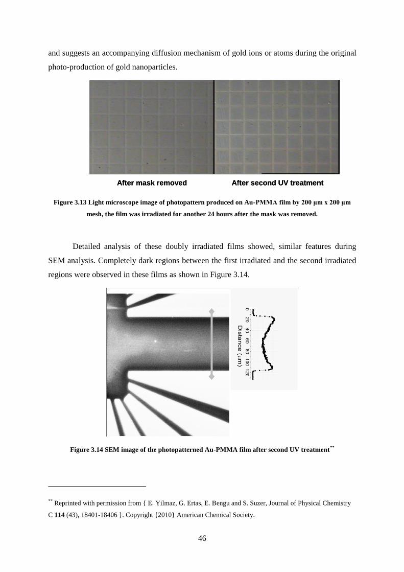
46
and suggests an accompanying diffusion mechanism of gold ions or atoms during the original
photo-production of gold nanoparticles.
Figure 3.13 Light microscope image of photopattern produced on Au-PMMA film by 200 μm x 200 μm
mesh, the film was irradiated for another 24 hours after the mask was removed.
Detailed analysis of these doubly irradiated films showed, similar features during
SEM analysis. Completely dark regions between the first irradiated and the second irradiated
regions were observed in these films as shown in Figure 3.14.
Figure 3.14 SEM image of the photopatterned Au-PMMA film after second UV treatment**
** Reprinted with permission from { E. Yilmaz, G. Ertas, E. Bengu and S. Suzer, Journal of Physical Chemistry
C 114 (43), 18401-18406 }. Copyright {2010} American Chemical Society.
After mask removed After second UV treatmentAfter mask removed After second UV treatment
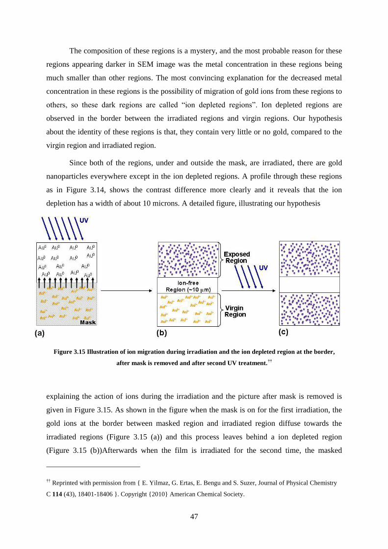
47
The composition of these regions is a mystery, and the most probable reason for these
regions appearing darker in SEM image was the metal concentration in these regions being
much smaller than other regions. The most convincing explanation for the decreased metal
concentration in these regions is the possibility of migration of gold ions from these regions to
others, so these dark regions are called “ion depleted regions”. Ion depleted regions are
observed in the border between the irradiated regions and virgin regions. Our hypothesis
about the identity of these regions is that, they contain very little or no gold, compared to the
virgin region and irradiated region.
Since both of the regions, under and outside the mask, are irradiated, there are gold
nanoparticles everywhere except in the ion depleted regions. A profile through these regions
as in Figure 3.14, shows the contrast difference more clearly and it reveals that the ion
depletion has a width of about 10 microns. A detailed figure, illustrating our hypothesis
Figure 3.15 Illustration of ion migration during irradiation and the ion depleted region at the border,
after mask is removed and after second UV treatment.††
explaining the action of ions during the irradiation and the picture after mask is removed is
given in Figure 3.15. As shown in the figure when the mask is on for the first irradiation, the
gold ions at the border between masked region and irradiated region diffuse towards the
irradiated regions (Figure 3.15 (a)) and this process leaves behind a ion depleted region
(Figure 3.15 (b))Afterwards when the film is irradiated for the second time, the masked
†† Reprinted with permission from { E. Yilmaz, G. Ertas, E. Bengu and S. Suzer, Journal of Physical Chemistry
C 114 (43), 18401-18406 }. Copyright {2010} American Chemical Society.
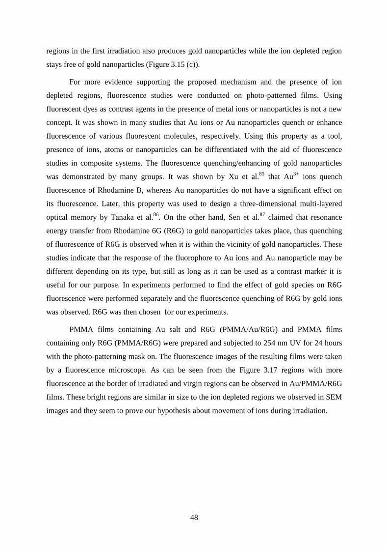
48
regions in the first irradiation also produces gold nanoparticles while the ion depleted region
stays free of gold nanoparticles (Figure 3.15 (c)).
For more evidence supporting the proposed mechanism and the presence of ion
depleted regions, fluorescence studies were conducted on photo-patterned films. Using
fluorescent dyes as contrast agents in the presence of metal ions or nanoparticles is not a new
concept. It was shown in many studies that Au ions or Au nanoparticles quench or enhance
fluorescence of various fluorescent molecules, respectively. Using this property as a tool,
presence of ions, atoms or nanoparticles can be differentiated with the aid of fluorescence
studies in composite systems. The fluorescence quenching/enhancing of gold nanoparticles
was demonstrated by many groups. It was shown by Xu et al.85
that Au3+
ions quench
fluorescence of Rhodamine B, whereas Au nanoparticles do not have a significant effect on
its fluorescence. Later, this property was used to design a three-dimensional multi-layered
optical memory by Tanaka et al.86
. On the other hand, Sen et al.87
claimed that resonance
energy transfer from Rhodamine 6G (R6G) to gold nanoparticles takes place, thus quenching
of fluorescence of R6G is observed when it is within the vicinity of gold nanoparticles. These
studies indicate that the response of the fluorophore to Au ions and Au nanoparticle may be
different depending on its type, but still as long as it can be used as a contrast marker it is
useful for our purpose. In experiments performed to find the effect of gold species on R6G
fluorescence were performed separately and the fluorescence quenching of R6G by gold ions
was observed. R6G was then chosen for our experiments.
PMMA films containing Au salt and R6G (PMMA/Au/R6G) and PMMA films
containing only R6G (PMMA/R6G) were prepared and subjected to 254 nm UV for 24 hours
with the photo-patterning mask on. The fluorescence images of the resulting films were taken
by a fluorescence microscope. As can be seen from the Figure 3.17 regions with more
fluorescence at the border of irradiated and virgin regions can be observed in Au/PMMA/R6G
films. These bright regions are similar in size to the ion depleted regions we observed in SEM
images and they seem to prove our hypothesis about movement of ions during irradiation.
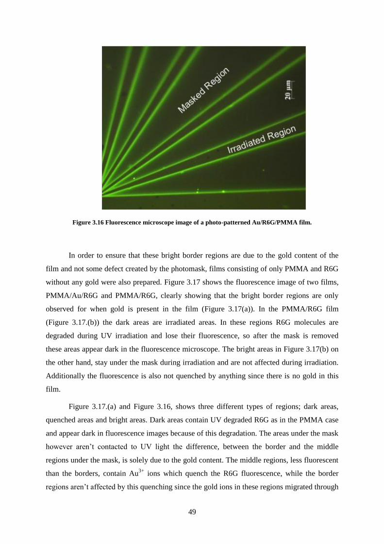
49
Figure 3.16 Fluorescence microscope image of a photo-patterned Au/R6G/PMMA film.
In order to ensure that these bright border regions are due to the gold content of the
film and not some defect created by the photomask, films consisting of only PMMA and R6G
without any gold were also prepared. Figure 3.17 shows the fluorescence image of two films,
PMMA/Au/R6G and PMMA/R6G, clearly showing that the bright border regions are only
observed for when gold is present in the film (Figure 3.17(a)). In the PMMA/R6G film
(Figure 3.17.(b)) the dark areas are irradiated areas. In these regions R6G molecules are
degraded during UV irradiation and lose their fluorescence, so after the mask is removed
these areas appear dark in the fluorescence microscope. The bright areas in Figure 3.17(b) on
the other hand, stay under the mask during irradiation and are not affected during irradiation.
Additionally the fluorescence is also not quenched by anything since there is no gold in this
film.
Figure 3.17.(a) and Figure 3.16, shows three different types of regions; dark areas,
quenched areas and bright areas. Dark areas contain UV degraded R6G as in the PMMA case
and appear dark in fluorescence images because of this degradation. The areas under the mask
however aren‟t contacted to UV light the difference, between the border and the middle
regions under the mask, is solely due to the gold content. The middle regions, less fluorescent
than the borders, contain Au3+
ions which quench the R6G fluorescence, while the border
regions aren‟t affected by this quenching since the gold ions in these regions migrated through
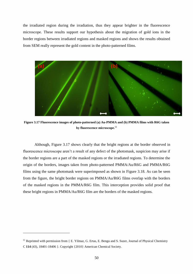
50
the irradiated region during the irradiation, thus they appear brighter in the fluorescence
microscope. These results support our hypothesis about the migration of gold ions in the
border regions between irradiated regions and masked regions and shows the results obtained
from SEM really represent the gold content in the photo-patterned films.
Figure 3.17 Fluorescence images of photo-patterned (a) Au-PMMA and (b) PMMA films with R6G taken
by fluorescence microscope.‡‡
Although, Figure 3.17 shows clearly that the bright regions at the border observed in
fluorescence microscope aren‟t a result of any defect of the photomask, suspicion may arise if
the border regions are a part of the masked regions or the irradiated regions. To determine the
origin of the borders, images taken from photo-patterned PMMA/Au/R6G and PMMA/R6G
films using the same photomask were superimposed as shown in Figure 3.18. As can be seen
from the figure, the bright border regions on PMMA/Au/R6G films overlap with the borders
of the masked regions in the PMMA/R6G film. This interception provides solid proof that
these bright regions in PMMA/Au/R6G film are the borders of the masked regions.
‡‡ Reprinted with permission from { E. Yilmaz, G. Ertas, E. Bengu and S. Suzer, Journal of Physical Chemistry
C 114 (43), 18401-18406 }. Copyright {2010} American Chemical Society.
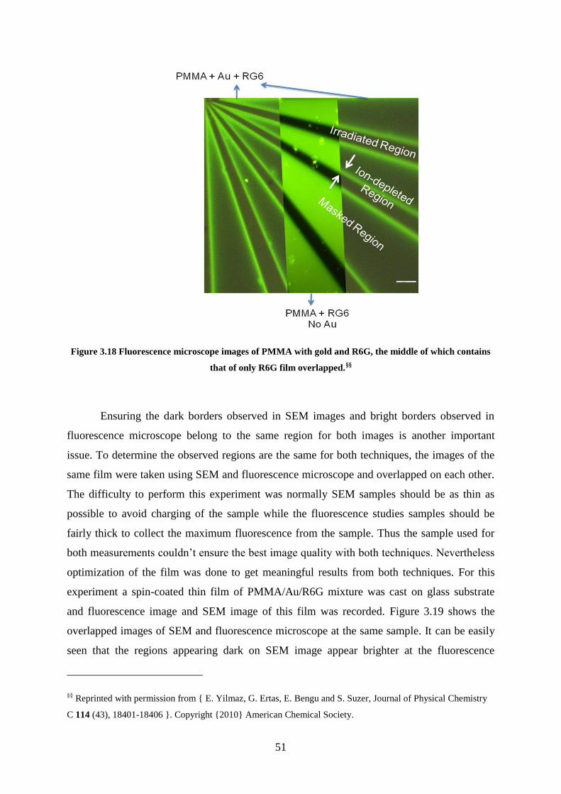
51
Figure 3.18 Fluorescence microscope images of PMMA with gold and R6G, the middle of which contains
that of only R6G film overlapped.§§
Ensuring the dark borders observed in SEM images and bright borders observed in
fluorescence microscope belong to the same region for both images is another important
issue. To determine the observed regions are the same for both techniques, the images of the
same film were taken using SEM and fluorescence microscope and overlapped on each other.
The difficulty to perform this experiment was normally SEM samples should be as thin as
possible to avoid charging of the sample while the fluorescence studies samples should be
fairly thick to collect the maximum fluorescence from the sample. Thus the sample used for
both measurements couldn‟t ensure the best image quality with both techniques. Nevertheless
optimization of the film was done to get meaningful results from both techniques. For this
experiment a spin-coated thin film of PMMA/Au/R6G mixture was cast on glass substrate
and fluorescence image and SEM image of this film was recorded. Figure 3.19 shows the
overlapped images of SEM and fluorescence microscope at the same sample. It can be easily
seen that the regions appearing dark on SEM image appear brighter at the fluorescence
§§ Reprinted with permission from { E. Yilmaz, G. Ertas, E. Bengu and S. Suzer, Journal of Physical Chemistry
C 114 (43), 18401-18406 }. Copyright {2010} American Chemical Society.
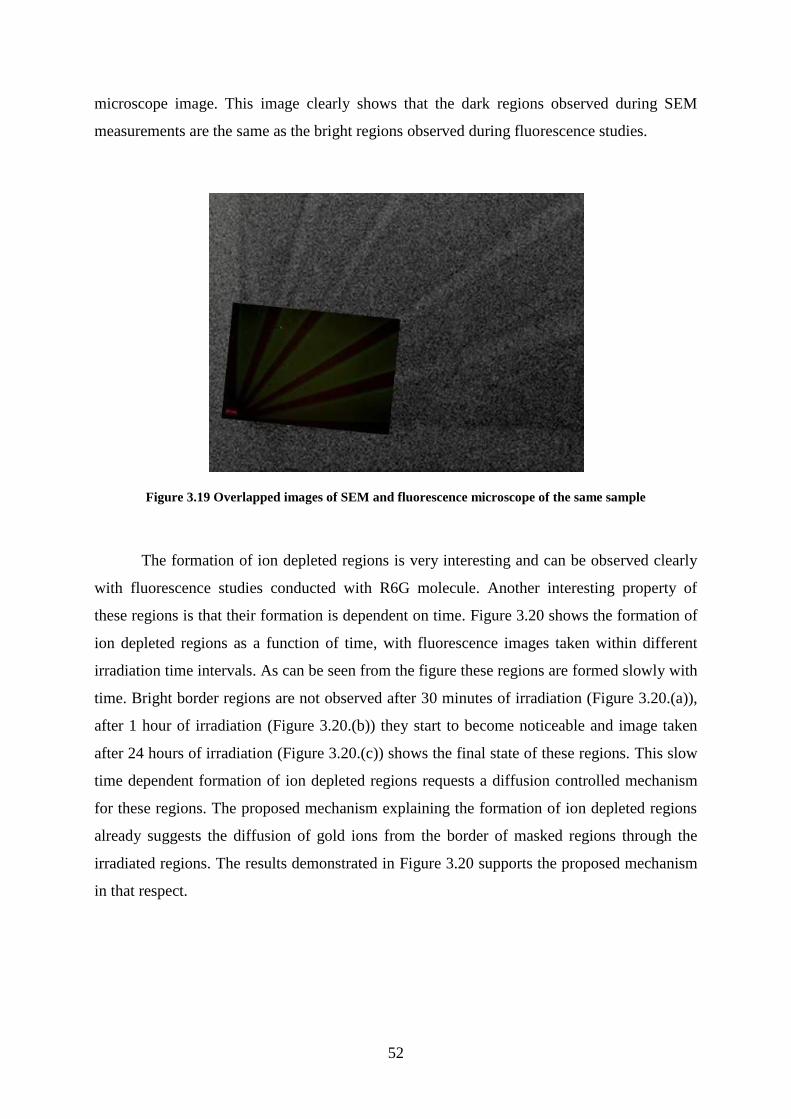
52
microscope image. This image clearly shows that the dark regions observed during SEM
measurements are the same as the bright regions observed during fluorescence studies.
Figure 3.19 Overlapped images of SEM and fluorescence microscope of the same sample
The formation of ion depleted regions is very interesting and can be observed clearly
with fluorescence studies conducted with R6G molecule. Another interesting property of
these regions is that their formation is dependent on time. Figure 3.20 shows the formation of
ion depleted regions as a function of time, with fluorescence images taken within different
irradiation time intervals. As can be seen from the figure these regions are formed slowly with
time. Bright border regions are not observed after 30 minutes of irradiation (Figure 3.20.(a)),
after 1 hour of irradiation (Figure 3.20.(b)) they start to become noticeable and image taken
after 24 hours of irradiation (Figure 3.20.(c)) shows the final state of these regions. This slow
time dependent formation of ion depleted regions requests a diffusion controlled mechanism
for these regions. The proposed mechanism explaining the formation of ion depleted regions
already suggests the diffusion of gold ions from the border of masked regions through the
irradiated regions. The results demonstrated in Figure 3.20 supports the proposed mechanism
in that respect.
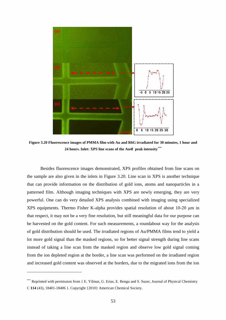
53
Figure 3.20 Fluorescence images of PMMA film with Au and R6G irradiated for 30 minutes, 1 hour and
24 hours. Inlet: XPS line scans of the Au4f peak intensity***
Besides fluorescence images demonstrated, XPS profiles obtained from line scans on
the sample are also given in the inlets in Figure 3.20. Line scan in XPS is another technique
that can provide information on the distribution of gold ions, atoms and nanoparticles in a
patterned film. Although imaging techniques with XPS are newly emerging, they are very
powerful. One can do very detailed XPS analysis combined with imaging using specialized
XPS equipments. Thermo Fisher K-alpha provides spatial resolution of about 10-20 μm in
that respect, it may not be a very fine resolution, but still meaningful data for our purpose can
be harvested on the gold content. For such measurements, a roundabout way for the analysis
of gold distribution should be used. The irradiated regions of Au/PMMA films tend to yield a
lot more gold signal than the masked regions, so for better signal strength during line scans
instead of taking a line scan from the masked region and observe low gold signal coming
from the ion depleted region at the border, a line scan was performed on the irradiated region
and increased gold content was observed at the borders, due to the migrated ions from the ion
*** Reprinted with permission from { E. Yilmaz, G. Ertas, E. Bengu and S. Suzer, Journal of Physical Chemistry
C 114 (43), 18401-18406 }. Copyright {2010} American Chemical Society.
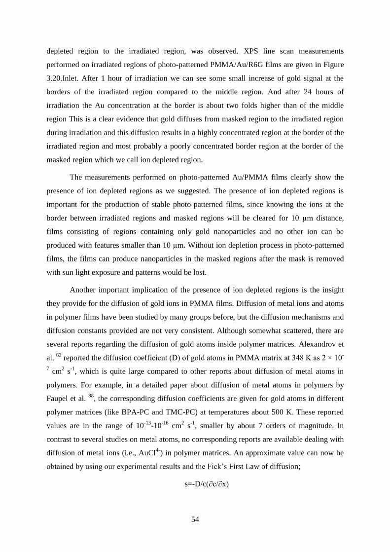
54
depleted region to the irradiated region, was observed. XPS line scan measurements
performed on irradiated regions of photo-patterned PMMA/Au/R6G films are given in Figure
3.20.Inlet. After 1 hour of irradiation we can see some small increase of gold signal at the
borders of the irradiated region compared to the middle region. And after 24 hours of
irradiation the Au concentration at the border is about two folds higher than of the middle
region This is a clear evidence that gold diffuses from masked region to the irradiated region
during irradiation and this diffusion results in a highly concentrated region at the border of the
irradiated region and most probably a poorly concentrated border region at the border of the
masked region which we call ion depleted region.
The measurements performed on photo-patterned Au/PMMA films clearly show the
presence of ion depleted regions as we suggested. The presence of ion depleted regions is
important for the production of stable photo-patterned films, since knowing the ions at the
border between irradiated regions and masked regions will be cleared for 10 µm distance,
films consisting of regions containing only gold nanoparticles and no other ion can be
produced with features smaller than 10 µm. Without ion depletion process in photo-patterned
films, the films can produce nanoparticles in the masked regions after the mask is removed
with sun light exposure and patterns would be lost.
Another important implication of the presence of ion depleted regions is the insight
they provide for the diffusion of gold ions in PMMA films. Diffusion of metal ions and atoms
in polymer films have been studied by many groups before, but the diffusion mechanisms and
diffusion constants provided are not very consistent. Although somewhat scattered, there are
several reports regarding the diffusion of gold atoms inside polymer matrices. Alexandrov et
al. 63
reported the diffusion coefficient (D) of gold atoms in PMMA matrix at 348 K as 2 × 10-
7 cm
2 s
-1, which is quite large compared to other reports about diffusion of metal atoms in
polymers. For example, in a detailed paper about diffusion of metal atoms in polymers by
Faupel et al. 88
, the corresponding diffusion coefficients are given for gold atoms in different
polymer matrices (like BPA-PC and TMC-PC) at temperatures about 500 K. These reported
values are in the range of 10-13
-10-16
cm2 s
-1, smaller by about 7 orders of magnitude. In
contrast to several studies on metal atoms, no corresponding reports are available dealing with
diffusion of metal ions (i.e., AuCl4-
) in polymer matrices. An approximate value can now be
obtained by using our experimental results and the Fick‟s First Law of diffusion;
s=-D/c(∂c/∂x)
55
where s denotes the terminal speed of the ions, D is the diffusion coefficient, c is the
concentration, and ∂c/∂x is the concentration gradient. For a movement of 10 μm = 0.001 cm
within 24 h, we can get an estimate of 1.2 × 10⁻⁸
cm/s for s, and an upper limiting value for
the concentration gradient can be estimated as c /10 μm, by assuming total consumption of the
ions within the irradiated regions.
D = 1.2 x 10⁻⁸
cm / s*0.001 cm
This rough procedure yields an unreasonably large diffusion constant of 10-11
cm2/s for ions to
move in polymer matrices at RT. The reason behind this large estimation may be a driving
force for the gold ions to move from masked regions to irradiated regions. Such a force would
definitely accelerate the motion of gold ions and may result in diffusion constants much larger
at room temperature.
It is well-known that gold atoms tend to come together, following their photoreduction
step, which results in formation of gold nanoparticles, because of their large cohesive energy
(366 kJ/mol), but we are yet to know of a factor to force the gold ions to diffuse at a 10 μm
distance from the masked regions toward the irradiated ones at RT, and in the absence of
external electrical potentials. Development of an electrochemical potential due to depletion of
ions as result of photoreduction in the irradiated regions can be thought of as the
thermodynamic driving force, but its magnitude can be estimated as ca. 120 mV (11 kJ/mol)
for an extreme concentration difference of a factor of 100 between the two regions. Even this
value is about 30 times smaller than the driving force for the gold atoms. Thus the nature of
the driving force behind this unusual movement of gold nanoparticles is yet to known but we
can observe its effects in our photo-patterned films with the formation of ion depleted regions.
In addition to the preparation of gold nanoparticles in PMMA films, we can also
produce gold nanoparticles in PVA films as mentioned beforehand. Such films can also be
photo-patterned using masking method. In order to see if there were similar ion depletion
processes in PVA/Au films, PVA/Au/R6G films were prepared and photo-patterned by UV
irradiation. SEM images and fluorescence images of PVA/Au/R6G film can be seen in Figure
3.21. As can be seen from the figure, both SEM image shows dark regions at the borders and
fluorescence image shows the bright regions at the borders like those observed in the PMMA
films. This result ensures us that similar ion depletion process also takes place in PVA matrix.
This result shows that the ion depletion process is not specific to the polymer, but it is
probably a process depending only on the gold ions and their reduction processes.
56
Figure 3.21 Photo-patterned PVA film containing Au nanoparticles and R6G, left hand-side shows SEM
image right hand-side shows fluorescence image.†††
As a conclusion, in this section photo-patterning of PMMA films with gold
nanoparticles was demonstrated. Photo-patterned thick Au/PMMA films were imaged in
optical microscope while for thin photo-patterned films SEM imaging was employed. During
SEM studies dark regions, between masked regions and irradiated regions of the photo-
patterned films, were observed. Close investigation of these dark regions with fluorescence
studies, hinting the gold content of the patterned films, concluded the formation of ion
depleted region between masked regions and irradiated regions, due to the migration of gold
ions from the masked regions through the irradiated regions. Ion depleted region are as wide
as 10 µm, which is surprisingly large for an ion to diffuse through a polymeric substance. The
presence of ion depleted regions is especially important for the production of durable photo-
patterned films with feature size less than 10 µm and using the data we obtain during the
formation of ion depleted regions, diffusion constant of the gold ions in PMMA matrix can be
calculated.
††† Reprinted with permission from { E. Yilmaz, G. Ertas, E. Bengu and S. Suzer, Journal of Physical Chemistry
C 114 (43), 18401-18406 }. Copyright {2010} American Chemical Society.
57
3.3 Effect of Gold Nanoparticles on the Dielectric Properties of PMMA
Normally PMMA is used as a dielectric component in electronic applications due to
its high resistivity. 89
On the other hand, the change in resistivity of PMMA by the addition of
conducting species to the matrix is also point of concern. 90, 91
Also, the effect of gold NPs on
PMMA conductivity is a well-discussed issue in previous studies of different groups.
Abyaneh et al. 92
showed the decreased resistivity of PMMA films with increasing gold NP
content. In their experiments oleylamine capped gold NPs were mixed with PMMA by
different weight percentage ratios and I-V measurements were performed with a Keithley 238
current/voltage sourcemeter unit. In another recent study, the increased conductivity of
PMMA by gold ions was studied by Salvadori et al. 93
with a buried conducting layer of
metal/polymer nanocomposite which was formed by very low energy gold ion
implementation. The measurement was made through electrical contacts attached to the film
with silver glue and covered by a thin Pt film for better contact. The gold ions penetrated
through 2.7 nm depth of the 50 nm PMMA film and it was shown that the conductivity of
PMMA increased drastically with the increasing amount of gold ions within the polymer. In
our study, we focus mainly on the charging properties of PMMA and Au NPs/PMMA films to
understand the effect of Au NPs on the electrical properties of PMMA films and we present a
new method to investigate the conductivity of gold nanoparticle-PMMA composites using
XPS.
Using charging as a tool to investigate the resistivity of PMMA films in XPS has
many advantages. The currents measured from polymer films are usually very low in the
range of nanoamperes due to high resistivity. The common method of measuring resistivity of
a film, the I-V measurement, needs very good electrical contacts to the sample film and
sensitive equipment to perform a meaningful measurement. Additionally the measurement
must be insulated from the surroundings so that the measurement is not altered by the
environmental factors. At the other hand, XPS measurements don‟t need taxing contacts,
since the information comes directly from the surface of the film. Also needless to say that,
the sample is already isolated from the surrounding factors. Hence, more reliable results can
be obtained using XPS as a tool for resistivity and capacitance measurements of insulating
samples.
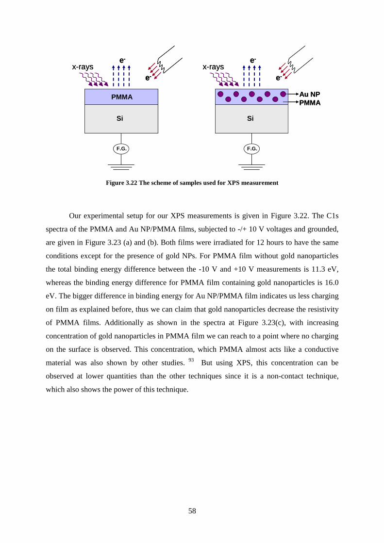
58
Figure 3.22 The scheme of samples used for XPS measurement
Our experimental setup for our XPS measurements is given in Figure 3.22. The C1s
spectra of the PMMA and Au NP/PMMA films, subjected to -/+ 10 V voltages and grounded,
are given in Figure 3.23 (a) and (b). Both films were irradiated for 12 hours to have the same
conditions except for the presence of gold NPs. For PMMA film without gold nanoparticles
the total binding energy difference between the -10 V and +10 V measurements is 11.3 eV,
whereas the binding energy difference for PMMA film containing gold nanoparticles is 16.0
eV. The bigger difference in binding energy for Au NP/PMMA film indicates us less charging
on film as explained before, thus we can claim that gold nanoparticles decrease the resistivity
of PMMA films. Additionally as shown in the spectra at Figure 3.23(c), with increasing
concentration of gold nanoparticles in PMMA film we can reach to a point where no charging
on the surface is observed. This concentration, which PMMA almost acts like a conductive
material was also shown by other studies. 93
But using XPS, this concentration can be
observed at lower quantities than the other techniques since it is a non-contact technique,
which also shows the power of this technique.
e-
e-
x-rays
e-
e-
x-rays
PMMA
Si Si
Au NP
PMMA
F.G. F.G.
e-
e-
x-rays
e-e-
e-
x-rays
PMMA
Si Si
Au NP
PMMA
F.G. F.G.
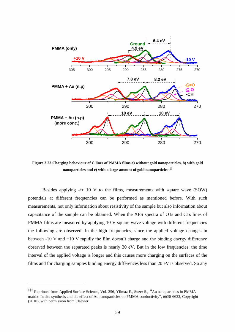
59
Figure 3.23 Charging behaviour of C lines of PMMA films a) without gold nanoparticles, b) with gold
nanoparticles and c) with a large amount of gold nanoparticles‡‡‡
Besides applying -/+ 10 V to the films, measurements with square wave (SQW)
potentials at different frequencies can be performed as mentioned before. With such
measurements, not only information about resistivity of the sample but also information about
capacitance of the sample can be obtained. When the XPS spectra of O1s and C1s lines of
PMMA films are measured by applying 10 V square wave voltage with different frequencies
the following are observed: In the high frequencies, since the applied voltage changes in
between -10 V and +10 V rapidly the film doesn‟t charge and the binding energy difference
observed between the separated peaks is nearly 20 eV. But in the low frequencies, the time
interval of the applied voltage is longer and this causes more charging on the surfaces of the
films and for charging samples binding energy differences less than 20 eV is observed. So any
‡‡‡ Reprinted from Applied Surface Science, Vol. 256, Yilmaz E., Suzer S., “Au nanoparticles in PMMA
matrix: In situ synthesis and the effect of Au nanoparticles on PMMA conductivity”, 6630-6633, Copyright
(2010), with permission from Elsevier.
270280290300
7.8 eV
-C=O-C-O
PMMA (only)
PMMA + Au (n.p)
8.2 eV
-CH
+10 V
10 eV10 eVPMMA + Au (n.p)
(more conc.)
270280290300
-10 V
6.4 eVGround4.9 eV
305 300 295 290 285 280 275 270
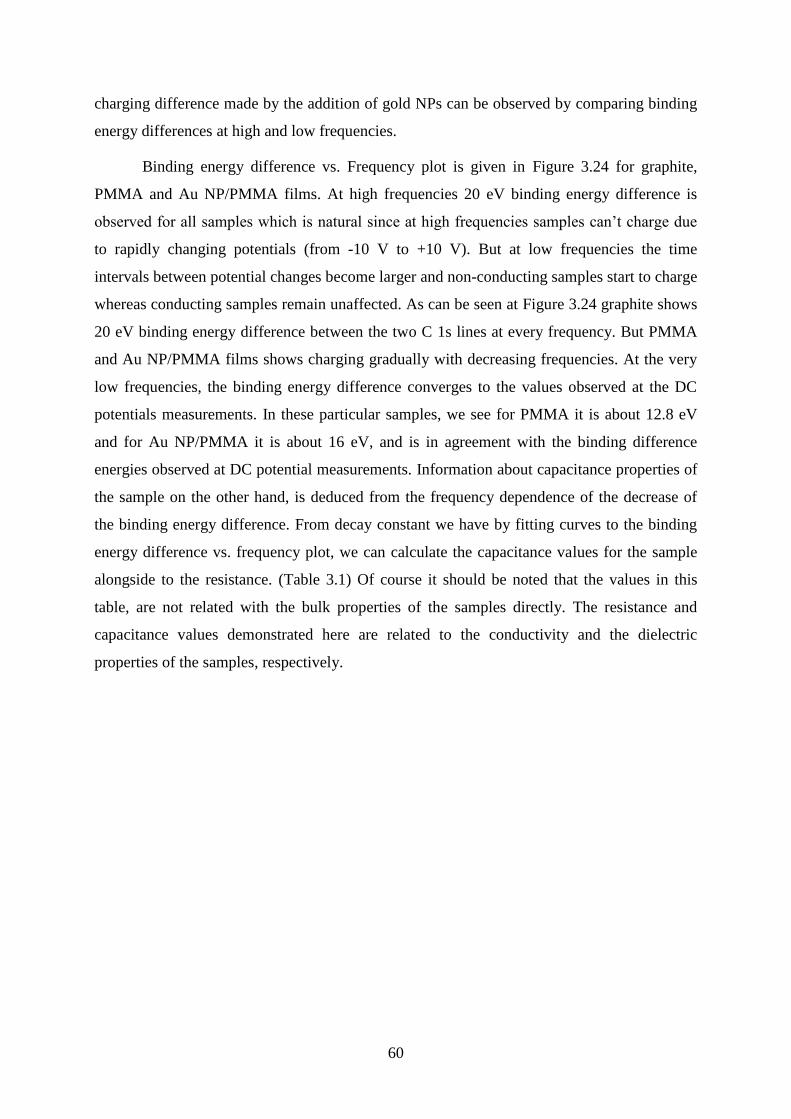
60
charging difference made by the addition of gold NPs can be observed by comparing binding
energy differences at high and low frequencies.
Binding energy difference vs. Frequency plot is given in Figure 3.24 for graphite,
PMMA and Au NP/PMMA films. At high frequencies 20 eV binding energy difference is
observed for all samples which is natural since at high frequencies samples can‟t charge due
to rapidly changing potentials (from -10 V to +10 V). But at low frequencies the time
intervals between potential changes become larger and non-conducting samples start to charge
whereas conducting samples remain unaffected. As can be seen at Figure 3.24 graphite shows
20 eV binding energy difference between the two C 1s lines at every frequency. But PMMA
and Au NP/PMMA films shows charging gradually with decreasing frequencies. At the very
low frequencies, the binding energy difference converges to the values observed at the DC
potentials measurements. In these particular samples, we see for PMMA it is about 12.8 eV
and for Au NP/PMMA it is about 16 eV, and is in agreement with the binding difference
energies observed at DC potential measurements. Information about capacitance properties of
the sample on the other hand, is deduced from the frequency dependence of the decrease of
the binding energy difference. From decay constant we have by fitting curves to the binding
energy difference vs. frequency plot, we can calculate the capacitance values for the sample
alongside to the resistance. (Table 3.1) Of course it should be noted that the values in this
table, are not related with the bulk properties of the samples directly. The resistance and
capacitance values demonstrated here are related to the conductivity and the dielectric
properties of the samples, respectively.
61
Figure 3.24 Measurement of dielectric behaviour of Graphite, PMMA and Au NP/PMMA films with SQW
voltages at different frequencies.§§§
Table 3.1 Resistance and capacitance values calculated for Au NP/PMMA and PMMA films with SQW
measurements
R C
PMMA 2.25 Mohm 6 μF
Au NP/PMMA 0.9 Mohm 20 μF
Another interesting feature observed at SQW measurements is the off-set in the line
positions of charging samples at high frequencies. Figure 3.25 shows such a measurement
performed on PMMA and Au NP/PMMA films and compared to conducting graphite
spectrum. Off-set in line positions at non-conducting samples is observed because of IR-drop
§§§ Reprinted from Applied Surface Science, Vol. 256, Yilmaz E., Suzer S., “Au nanoparticles in PMMA matrix:
In situ synthesis and the effect of Au nanoparticles on PMMA conductivity”, 6630-6633, Copyright (2010), with
permission from Elsevier.
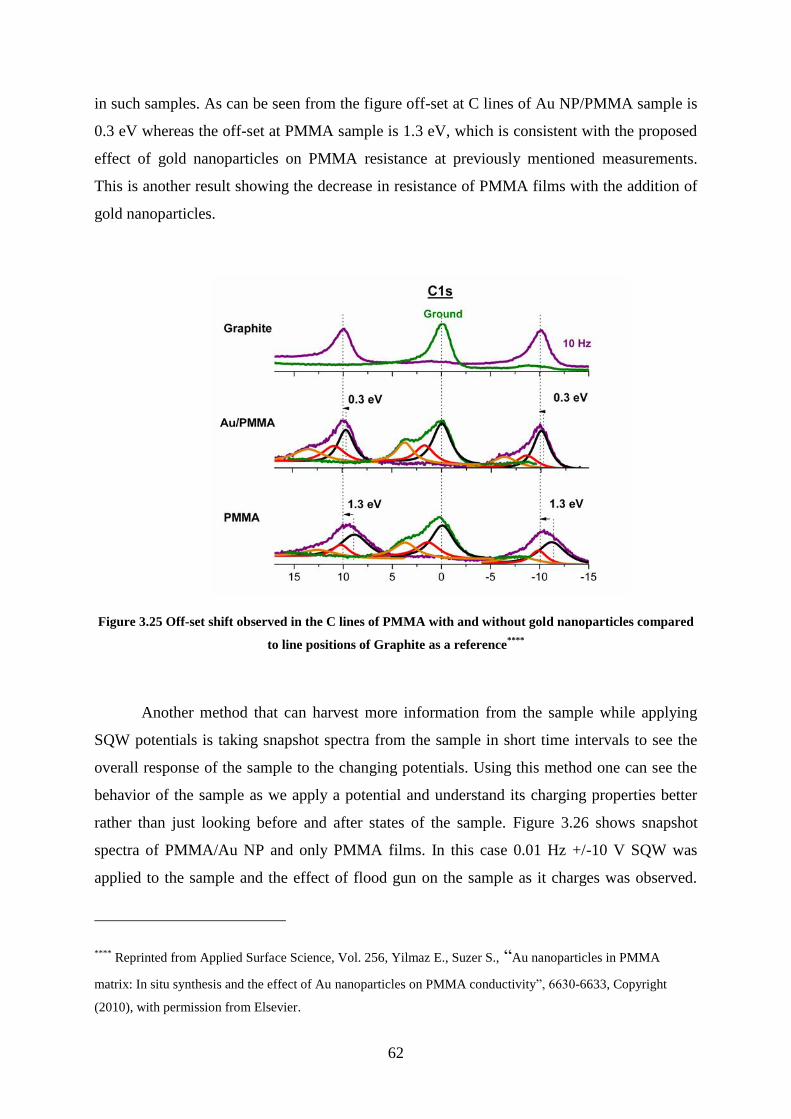
62
in such samples. As can be seen from the figure off-set at C lines of Au NP/PMMA sample is
0.3 eV whereas the off-set at PMMA sample is 1.3 eV, which is consistent with the proposed
effect of gold nanoparticles on PMMA resistance at previously mentioned measurements.
This is another result showing the decrease in resistance of PMMA films with the addition of
gold nanoparticles.
Figure 3.25 Off-set shift observed in the C lines of PMMA with and without gold nanoparticles compared
to line positions of Graphite as a reference****
Another method that can harvest more information from the sample while applying
SQW potentials is taking snapshot spectra from the sample in short time intervals to see the
overall response of the sample to the changing potentials. Using this method one can see the
behavior of the sample as we apply a potential and understand its charging properties better
rather than just looking before and after states of the sample. Figure 3.26 shows snapshot
spectra of PMMA/Au NP and only PMMA films. In this case 0.01 Hz +/-10 V SQW was
applied to the sample and the effect of flood gun on the sample as it charges was observed.
**** Reprinted from Applied Surface Science, Vol. 256, Yilmaz E., Suzer S., “Au nanoparticles in PMMA
matrix: In situ synthesis and the effect of Au nanoparticles on PMMA conductivity”, 6630-6633, Copyright
(2010), with permission from Elsevier.
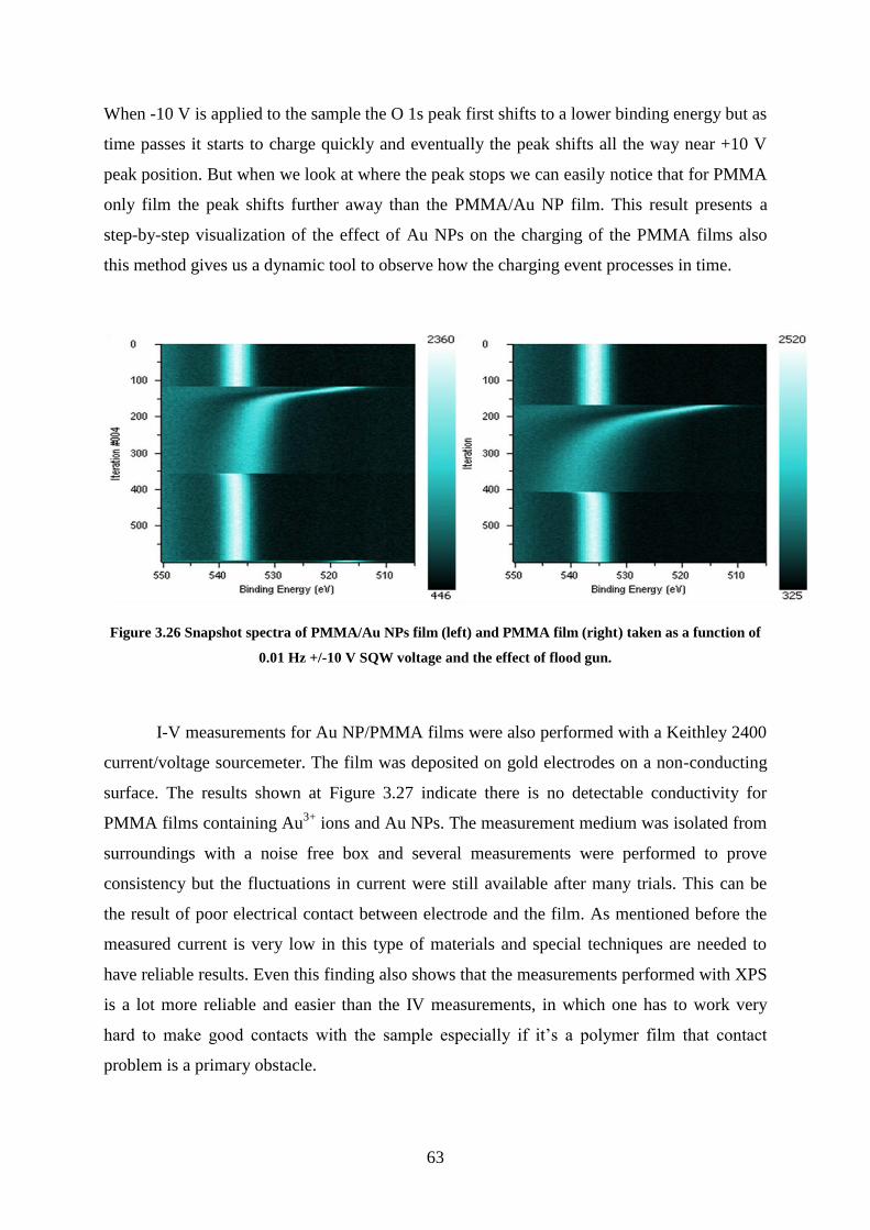
63
When -10 V is applied to the sample the O 1s peak first shifts to a lower binding energy but as
time passes it starts to charge quickly and eventually the peak shifts all the way near +10 V
peak position. But when we look at where the peak stops we can easily notice that for PMMA
only film the peak shifts further away than the PMMA/Au NP film. This result presents a
step-by-step visualization of the effect of Au NPs on the charging of the PMMA films also
this method gives us a dynamic tool to observe how the charging event processes in time.
Figure 3.26 Snapshot spectra of PMMA/Au NPs film (left) and PMMA film (right) taken as a function of
0.01 Hz +/-10 V SQW voltage and the effect of flood gun.
I-V measurements for Au NP/PMMA films were also performed with a Keithley 2400
current/voltage sourcemeter. The film was deposited on gold electrodes on a non-conducting
surface. The results shown at Figure 3.27 indicate there is no detectable conductivity for
PMMA films containing Au3+
ions and Au NPs. The measurement medium was isolated from
surroundings with a noise free box and several measurements were performed to prove
consistency but the fluctuations in current were still available after many trials. This can be
the result of poor electrical contact between electrode and the film. As mentioned before the
measured current is very low in this type of materials and special techniques are needed to
have reliable results. Even this finding also shows that the measurements performed with XPS
is a lot more reliable and easier than the IV measurements, in which one has to work very
hard to make good contacts with the sample especially if it‟s a polymer film that contact
problem is a primary obstacle.
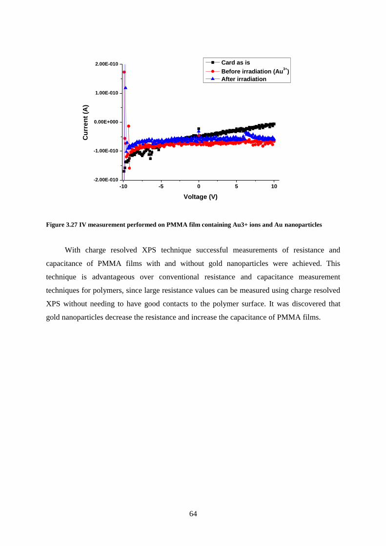
64
Figure 3.27 IV measurement performed on PMMA film containing Au3+ ions and Au nanoparticles
With charge resolved XPS technique successful measurements of resistance and
capacitance of PMMA films with and without gold nanoparticles were achieved. This
technique is advantageous over conventional resistance and capacitance measurement
techniques for polymers, since large resistance values can be measured using charge resolved
XPS without needing to have good contacts to the polymer surface. It was discovered that
gold nanoparticles decrease the resistance and increase the capacitance of PMMA films.
-10 -5 0 5 10
-2.00E-010
-1.00E-010
0.00E+000
1.00E-010
2.00E-010
Cu
rren
t (A
)
Voltage (V)
Card as is
Before irradiation (Au3+
)
After irradiation
65
3.4 Extra electrons on the PMMA Surface: Pendant Groups are Affected
More than Skeleton Carbons
Electrification or electret formation is well-known to men for more than 2500 years.
An “electret” is defined as a material that develops a permanent electrostatic potential due to
extra charges, or has a permanent dipole moment. Electrons are spatially localized within
atoms and molecules occupying atomic and molecular orbitals, and when larger particles or
assemblies are considered interatomic and intermolecular delocalization of electrons becomes
important, and dictate the electrical properties of metals and to some extent of
semiconductors. However, for semiconductors additional electronic states due to doping or
defects, imperfections at their surfaces and/or grain boundaries, as well within the lattice,
commonly described as traps, impurity states, etc., contribute significantly to their electrical
properties. For insulating materials like polymers (PMMA, PTFE, PVDF), salts, metal oxides,
nitrides, and sulphides, etc., which are described as having larger band-gap values, where
electrons are localized, leading to extremely low conductivities. In these materials, other
electronic states, like interface and impurity states, defect sites, etc. completely dominate their
electrical properties. In addition, electrical properties of these materials are strongly
influenced by external stresses, like exposure to light, energetic particles, mechanical
distortions, milling, etc., which are attributed to insertion of localized electrons and/or ions at
interfaces, grain boundaries, cracks, or in bulk sites like cavities, which even lead to certain
chemical oxidation-reduction reactions. 75
Among these, contact electrification has recently
been in focus, due to the recent studies, proposing two different mechanisms as its cause,
being electron transfer as opposed to ions or materials transfer with sound experimental
findings on both side. 69-73
One can probe the charges on an insulator surface in different ways. Wiles et al.
proposes the use of an electrometer which measures the charge accumulated on a
ferromagnetic sphere as it rolls over the polymer surface surrounded by a Faraday cage. 94
While Liu et al. shows the presence of cryptoelectrons as they conduct redox reactions on the
surface of contact electrified polymers. 75
We are now proposing a different novel technique
for analyzing this problem by using charge resolved XPS technique. As mentioned earlier, the
charging on the surface can be controlled with the applied external bias, thus the response of
the polymer surface to the induced charges and the accommodation of these charges can be
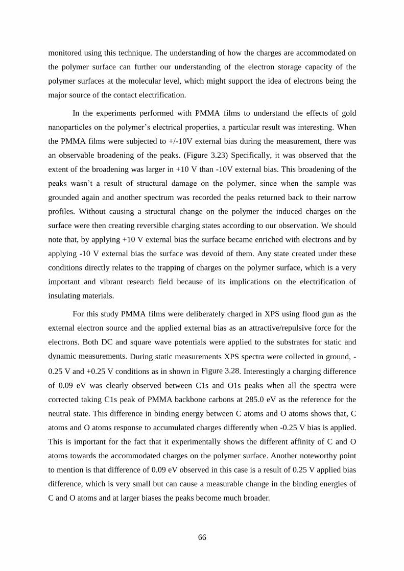
66
monitored using this technique. The understanding of how the charges are accommodated on
the polymer surface can further our understanding of the electron storage capacity of the
polymer surfaces at the molecular level, which might support the idea of electrons being the
major source of the contact electrification.
In the experiments performed with PMMA films to understand the effects of gold
nanoparticles on the polymer‟s electrical properties, a particular result was interesting. When
the PMMA films were subjected to +/-10V external bias during the measurement, there was
an observable broadening of the peaks. (Figure 3.23) Specifically, it was observed that the
extent of the broadening was larger in +10 V than -10V external bias. This broadening of the
peaks wasn‟t a result of structural damage on the polymer, since when the sample was
grounded again and another spectrum was recorded the peaks returned back to their narrow
profiles. Without causing a structural change on the polymer the induced charges on the
surface were then creating reversible charging states according to our observation. We should
note that, by applying +10 V external bias the surface became enriched with electrons and by
applying -10 V external bias the surface was devoid of them. Any state created under these
conditions directly relates to the trapping of charges on the polymer surface, which is a very
important and vibrant research field because of its implications on the electrification of
insulating materials.
For this study PMMA films were deliberately charged in XPS using flood gun as the
external electron source and the applied external bias as an attractive/repulsive force for the
electrons. Both DC and square wave potentials were applied to the substrates for static and
dynamic measurements. During static measurements XPS spectra were collected in ground, -
0.25 V and +0.25 V conditions as in shown in Figure 3.28. Interestingly a charging difference
of 0.09 eV was clearly observed between C1s and O1s peaks when all the spectra were
corrected taking C1s peak of PMMA backbone carbons at 285.0 eV as the reference for the
neutral state. This difference in binding energy between C atoms and O atoms shows that, C
atoms and O atoms response to accumulated charges differently when -0.25 V bias is applied.
This is important for the fact that it experimentally shows the different affinity of C and O
atoms towards the accommodated charges on the polymer surface. Another noteworthy point
to mention is that difference of 0.09 eV observed in this case is a result of 0.25 V applied bias
difference, which is very small but can cause a measurable change in the binding energies of
C and O atoms and at larger biases the peaks become much broader.
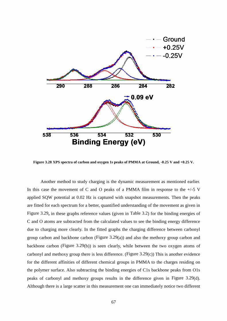
67
Figure 3.28 XPS spectra of carbon and oxygen 1s peaks of PMMA at Ground, -0.25 V and +0.25 V.
Another method to study charging is the dynamic measurement as mentioned earlier.
In this case the movement of C and O peaks of a PMMA film in response to the +/-5 V
applied SQW potential at 0.02 Hz is captured with snapshot measurements. Then the peaks
are fitted for each spectrum for a better, quantified understanding of the movement as given in
Figure 3.29, in these graphs reference values (given in Table 3.2) for the binding energies of
C and O atoms are subtracted from the calculated values to see the binding energy difference
due to charging more clearly. In the fitted graphs the charging difference between carbonyl
group carbon and backbone carbon (Figure 3.29(a)) and also the methoxy group carbon and
backbone carbon (Figure 3.29(b)) is seen clearly, while between the two oxygen atoms of
carbonyl and methoxy group there is less difference. (Figure 3.29(c)) This is another evidence
for the different affinities of different chemical groups in PMMA to the charges residing on
the polymer surface. Also subtracting the binding energies of C1s backbone peaks from O1s
peaks of carbonyl and methoxy groups results in the difference given in Figure 3.29(d).
Although there is a large scatter in this measurement one can immediately notice two different
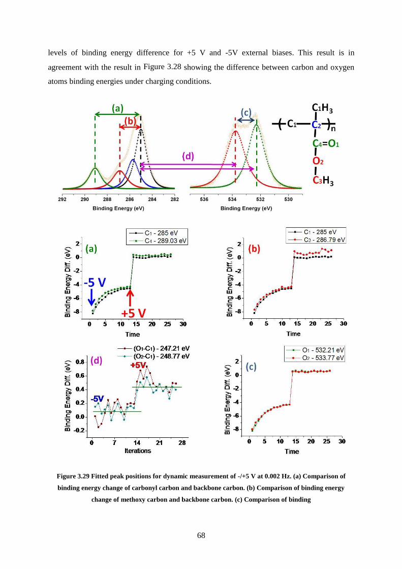
68
levels of binding energy difference for +5 V and -5V external biases. This result is in
agreement with the result in Figure 3.28 showing the difference between carbon and oxygen
atoms binding energies under charging conditions.
Figure 3.29 Fitted peak positions for dynamic measurement of -/+5 V at 0.002 Hz. (a) Comparison of
binding energy change of carbonyl carbon and backbone carbon. (b) Comparison of binding energy
change of methoxy carbon and backbone carbon. (c) Comparison of binding
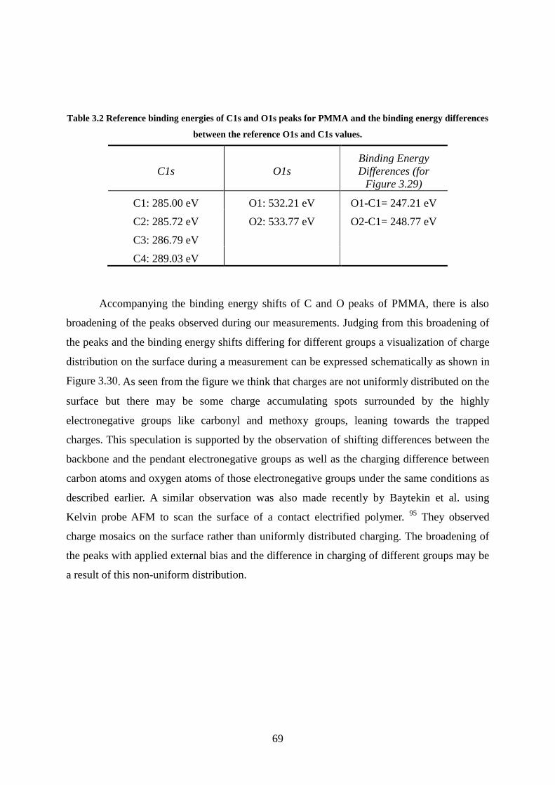
69
Table 3.2 Reference binding energies of C1s and O1s peaks for PMMA and the binding energy differences
between the reference O1s and C1s values.
C1s O1s
Binding Energy
Differences (for
Figure 3.29)
C1: 285.00 eV O1: 532.21 eV O1-C1= 247.21 eV
C2: 285.72 eV O2: 533.77 eV O2-C1= 248.77 eV
C3: 286.79 eV
C4: 289.03 eV
Accompanying the binding energy shifts of C and O peaks of PMMA, there is also
broadening of the peaks observed during our measurements. Judging from this broadening of
the peaks and the binding energy shifts differing for different groups a visualization of charge
distribution on the surface during a measurement can be expressed schematically as shown in
Figure 3.30. As seen from the figure we think that charges are not uniformly distributed on the
surface but there may be some charge accumulating spots surrounded by the highly
electronegative groups like carbonyl and methoxy groups, leaning towards the trapped
charges. This speculation is supported by the observation of shifting differences between the
backbone and the pendant electronegative groups as well as the charging difference between
carbon atoms and oxygen atoms of those electronegative groups under the same conditions as
described earlier. A similar observation was also made recently by Baytekin et al. using
Kelvin probe AFM to scan the surface of a contact electrified polymer. 95
They observed
charge mosaics on the surface rather than uniformly distributed charging. The broadening of
the peaks with applied external bias and the difference in charging of different groups may be
a result of this non-uniform distribution.
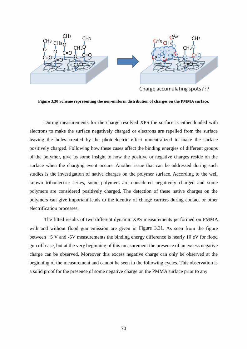
70
Figure 3.30 Scheme representing the non-uniform distribution of charges on the PMMA surface.
During measurements for the charge resolved XPS the surface is either loaded with
electrons to make the surface negatively charged or electrons are repelled from the surface
leaving the holes created by the photoelectric effect unneutralized to make the surface
positively charged. Following how these cases affect the binding energies of different groups
of the polymer, give us some insight to how the positive or negative charges reside on the
surface when the charging event occurs. Another issue that can be addressed during such
studies is the investigation of native charges on the polymer surface. According to the well
known triboelectric series, some polymers are considered negatively charged and some
polymers are considered positively charged. The detection of these native charges on the
polymers can give important leads to the identity of charge carriers during contact or other
electrification processes.
The fitted results of two different dynamic XPS measurements performed on PMMA
with and without flood gun emission are given in Figure 3.31. As seen from the figure
between +5 V and -5V measurements the binding energy difference is nearly 10 eV for flood
gun off case, but at the very beginning of this measurement the presence of an excess negative
charge can be observed. Moreover this excess negative charge can only be observed at the
beginning of the measurement and cannot be seen in the following cycles. This observation is
a solid proof for the presence of some negative charge on the PMMA surface prior to any
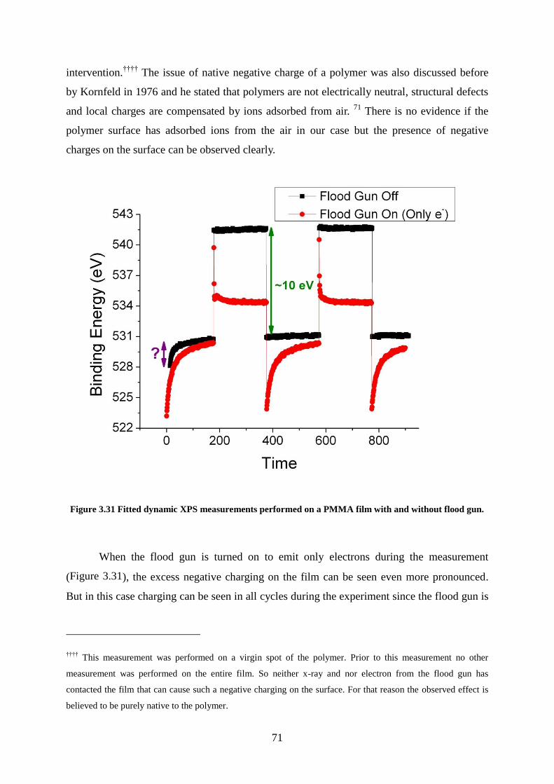
71
intervention.††††
The issue of native negative charge of a polymer was also discussed before
by Kornfeld in 1976 and he stated that polymers are not electrically neutral, structural defects
and local charges are compensated by ions adsorbed from air. 71
There is no evidence if the
polymer surface has adsorbed ions from the air in our case but the presence of negative
charges on the surface can be observed clearly.
Figure 3.31 Fitted dynamic XPS measurements performed on a PMMA film with and without flood gun.
When the flood gun is turned on to emit only electrons during the measurement
(Figure 3.31), the excess negative charging on the film can be seen even more pronounced.
But in this case charging can be seen in all cycles during the experiment since the flood gun is
†††† This measurement was performed on a virgin spot of the polymer. Prior to this measurement no other
measurement was performed on the entire film. So neither x-ray and nor electron from the flood gun has
contacted the film that can cause such a negative charging on the surface. For that reason the observed effect is
believed to be purely native to the polymer.
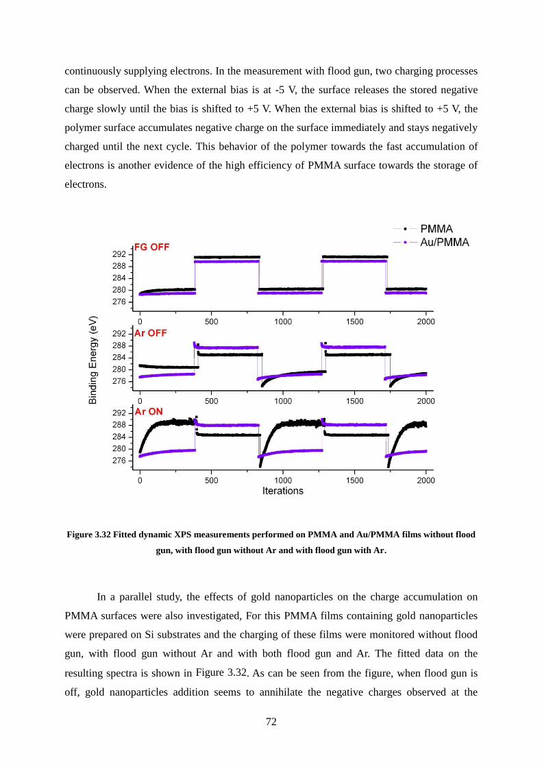
72
continuously supplying electrons. In the measurement with flood gun, two charging processes
can be observed. When the external bias is at -5 V, the surface releases the stored negative
charge slowly until the bias is shifted to +5 V. When the external bias is shifted to +5 V, the
polymer surface accumulates negative charge on the surface immediately and stays negatively
charged until the next cycle. This behavior of the polymer towards the fast accumulation of
electrons is another evidence of the high efficiency of PMMA surface towards the storage of
electrons.
Figure 3.32 Fitted dynamic XPS measurements performed on PMMA and Au/PMMA films without flood
gun, with flood gun without Ar and with flood gun with Ar.
In a parallel study, the effects of gold nanoparticles on the charge accumulation on
PMMA surfaces were also investigated, For this PMMA films containing gold nanoparticles
were prepared on Si substrates and the charging of these films were monitored without flood
gun, with flood gun without Ar and with both flood gun and Ar. The fitted data on the
resulting spectra is shown in Figure 3.32. As can be seen from the figure, when flood gun is
off, gold nanoparticles addition seems to annihilate the negative charges observed at the
73
beginning of the measurement. For flood gun on cases with and without Ar, the decreased
charge accumulation can be observed for the Au/PMMA film for both of the cases. These
results support our observations on the increasing of conductivity of PMMA films with gold
nanoparticle addition in our previously discussed studies.
The experiments performed with PMMA via charge resolved XPS technique, showed
the affinity of PMMA surface for the storage of electrons on the surface and it was also
observed that pendant groups and the backbone carbons response differently under charging
conditions, due to accumulation of charges. This difference in response is thought to be due to
the non-uniform distribution of charges on the polymer surface and relatively free movement
of the pendant groups. According to our hypothesis, the pendant groups can surround and
form charge accumulation spots and trap the surface charges in those spots. These
observations are important insights for furthering of our understanding of the mechanism of
electrification process on insulator materials like polymers and the effects of charge
accumulation at the molecular level. Additionally, in studies performed on PMMA films
containing gold nanoparticles, it was observed that gold nanoparticles decrease the charge
accumulation on the PMMA films.
74
4 Conclusions
In our studies, we have synthesized gold nanoparticles within polymer matrices using
photo irradiation. With this technique we obtain nanoparticle-polymer composites in one-step
without any further procedure. The reduction of Au3+
ions and formation of Au nanoparticles
are much slower in polymer matrix than in solution. So we can follow these two processes
separately using UV-Vis spectrometer and different factors affecting these processes may be
investigated. We probed the effects of heating, addition of another metal ion and
phototosensitizers on reduction and nucleation and growth, and we assessed the effects of the
given conditions on the reduction and nucleation and growth rates. Important information was
gained with these studies about the reduction mechanism of gold ions and the role of polymer
during reduction and nucleation and growth processes.
Photo-patterning is an important application of this synthesis method. Films of
different thicknesses with different feature sizes can be produced with light-impermeable
photomasks with this method. In our studies we discovered the presence of ion depleted
regions, which contain no gold ions or nanoparticles and are formed by migration of gold ions
at and near the border of the mask to the irradiated regions. Those regions can be observed as
dark border regions at SEM and additional verification on the content of the ion depleted
regions was also performed using fluorescence studies with Rhodamine 6G (R6G) molecules.
Fluorescence studies conducted with the addition of R6G molecules to the patterned films
concluded that, the ion depleted regions are indeed formed with the diffusion of gold ions at
the border of the masked regions through the irradiated regions.
For characterization of the films we also perform charging studies with XPS using DC
and SQW pulses. Thin films of PMMA with and without gold nanoparticles were probed with
applied DC potentials and it was observed that gold nanoparticles decrease the resistance of
PMMA films as shown by the previous studies in the literature. SQW potentials were also
used for getting additional information about the electric properties of such films. The SQW
potential measurements give us information about the capacitance properties of non-
conducting samples and in our experiments we saw the effect of gold nanoparticles on the
capacitance of the PMMA films with this method. Gold nanoparticles increased the
capacitance of PMMA films and decreased the resistance of the PMMA films as the summary
of our studies. These results were not new, but the point we want to emphasize is that these
measurements are very hard to do using normal electrical IV measurement since making good
75
electrical contacts to polymer films is difficult and also the measured current values are very
low. But in this study we reliably have shown that such measurements can be made by XPS
non-contact, more easily and accurately.
Another important process we investigated using charge resolved XPS technique is the
charge accumulation on the polymer surfaces and the effect of gold nanoparticles on this
process. Probing the charge accumulation on polymer surfaces may give us information on
the identity of charge carrying groups during contact and other forms of electrification of
electrets. The studies conducted to understand the charge accumulation on the PMMA surface
showed that, PMMA surface is very susceptible to accumulate negative charges on its surface
and there are even native negative charges on the surface prior to any treatment. This
observation partly supports the other studies claiming that the electrons are the charge carriers
during the contact electrification of insulators. Another observation done during these
experiments was that, the carbon and oxygen atoms of the pendant groups were reacting
differently than the carbon atoms of the polymer backbone when the surface was charged.
Presence of charge accumulation spots, surrounded by highly electronegative groups leaning
towards those charges, may be leading to this observation. Additionally the effect of gold
nanoparticles, on this charge accumulation process was also monitored during these studies.
And the decreasing charge accumulation with the addition of gold nanoparticles was
observed, supporting our previous observations on the effect of gold nanoparticle on the
conductivity of the PMMA films.
76
5 List of Abbreviations
DC Direct current
FG Flood gun
FT-IR Fourier Transform Infrared
NP Nanoparticle
PDMS Poly(dimethyl siloxane)
PMMA Poly(methyl methacrylate)
PS Poly(styrene)
PVA Poly(vinyl alcohol)
R6G Rhodamine 6G
SEM Scanning electron microscope
SERS Surface enhanced Raman spectroscopy
SPR Surface plasmon resonance
SQW Square wave
UV Ultraviolet
UV-Vis Ultraviolet-Visible
XPS X-ray photoelectron spectroscopy
77
6 References
1. M. C. Daniel and D. Astruc, Chemical Reviews 104 (1), 293-346 (2004).
2. K. Watanabe, D. Menzel, N. Nilius and H. J. Freund, Chemical Reviews 106 (10),
4301-4320 (2006).
3. A. N. Shipway, E. Katz and I. Willner, Chemphyschem 1 (1), 18-52 (2000).
4. R. Hoffmann, Angewandte Chemie-International Edition in English 26 (9), 846-878
(1987).
5. G. Schmid, Chem. Rev. 92 (8), 1709-1727 (1992).
6. M. Brust, D. Bethell, C. J. Kiely and D. J. Schiffrin, Langmuir 14 (19), 5425-5429
(1998).
7. T. Goodson, O. Varnavski and Y. Wang, International Reviews in Physical Chemistry
23 (1), 109-150 (2004).
8. X. Li, J. W. M. Chon and M. Gu, Australian Journal of Chemistry 61 (5), 317-323
(2008).
9. A. T. Bell, Science 299 (5613), 1688-1691 (2003).
10. M. S. Chen and D. W. Goodman, Science 306 (5694), 252-255 (2004).
11. L. He, M. D. Musick, S. R. Nicewarner, F. G. Salinas, S. J. Benkovic, M. J. Natan and
C. D. Keating, Journal of the American Chemical Society 122 (38), 9071-9077 (2000).
12. R. P. Bagwe, X. J. Zhao and W. H. Tan, Journal of Dispersion Science and
Technology 24 (3-4), 453-464 (2003).
13. M. Haruta, T. Kobayashi, H. Sano and N. Yamada, Chem. Lett. (2), 405-408 (1987).
14. M. Haruta, N. Yamada, T. Kobayashi and S. Iijima, J. Catal. 115 (2), 301-309 (1989).
15. H. Sakurai and M. Haruta, Catalysis Today 29 (1-4), 361-365 (1996).
16. A. Ueda, T. Oshima and M. Haruta, Applied Catalysis B-Environmental 12 (2-3), 81-
93 (1997).
17. T. Sato, H. Ahmed, D. Brown and B. F. G. Johnson, J. Appl. Phys. 82 (2), 696-701
(1997).
78
18. L. E. Brus, M. Bawendi, W. L. Wilson, L. Rothberg, P. J. Carroll, T. M. Jedju and M.
L. Steigerwald, Abstracts of Papers of the American Chemical Society 201, 409-INOR
(1991).
19. L. F. Chi, M. Hartig, T. Drechsler, T. Schwaack, C. Seidel, H. Fuchs and G. Schmid,
Applied Physics a-Materials Science & Processing 66, S187-S190 (1998).
20. M. Valden, X. Lai and D. W. Goodman, Science 281 (5383), 1647-1650 (1998).
21. A. P. Alivisatos, K. P. Johnsson, X. G. Peng, T. E. Wilson, C. J. Loweth, M. P.
Bruchez and P. G. Schultz, Nature 382 (6592), 609-611 (1996).
22. G. P. Mitchell, C. A. Mirkin and R. L. Letsinger, Journal of the American Chemical
Society 121 (35), 8122-8123 (1999).
23. T. A. Taton, R. C. Mucic, C. A. Mirkin and R. L. Letsinger, Journal of the American
Chemical Society 122 (26), 6305-6306 (2000).
24. Y. W. C. Cao, R. C. Jin and C. A. Mirkin, Science 297 (5586), 1536-1540 (2002).
25. A. Campion and P. Kambhampati, Chem. Soc. Rev. 27 (4), 241-250 (1998).
26. Y. J. Kim, R. C. Johnson and J. T. Hupp, Nano Letters 1 (4), 165-167 (2001).
27. C. Guan, C. L. Lu, Y. R. Cheng, S. Y. Song and B. Yang, J. Mater. Chem. 19 (5), 617-
621 (2009).
28. C. L. Lu, C. Guan, Y. F. Liu, Y. R. Cheng and B. Yang, Chemistry of Materials 17
(9), 2448-2454 (2005).
29. Y. Imai, A. Terahara, Y. Hakuta, K. Matsui, H. Hayashi and N. Ueno, Polymer
Journal 42 (2), 179-184 (2010).
30. J. L. H. Chau, C. T. Tung, Y. M. Lin and A. K. Li, Mater. Lett. 62 (19), 3416-3418
(2008).
31. Y. F. Liu, C. L. Lu, M. J. Li, L. Zhang and B. Yang, Colloids and Surfaces a-
Physicochemical and Engineering Aspects 328 (1-3), 67-72 (2008).
32. T. Hanemann, J. Hausselt and E. Ritzhaupt-Kleissl, Microsystem Technologies-
Micro-and Nanosystems-Information Storage and Processing Systems 15 (3), 421-427
(2009).
79
33. Y. Q. Li, Y. Yang, S. Y. Fu, X. Y. Yi, L. C. Wang and H. D. Chen, Journal of
Physical Chemistry C 112 (47), 18616-18622 (2008).
34. H. M. Xiong, Y. Xu, O. G. Ren and Y. Y. Xia, Journal of the American Chemical
Society 130 (24), 7522-+ (2008).
35. R. F. Ziolo, E. P. Giannelis and R. D. Shull, Nanostructured Materials 3 (1-6), 85-92
(1993).
36. R. F. Ziolo, E. P. Giannelis, B. A. Weinstein, M. P. Ohoro, B. N. Ganguly, V.
Mehrotra, M. W. Russell and D. R. Huffman, Science 257 (5067), 219-223 (1992).
37. C. M. Yang, H. Y. Li, D. B. Xiong and Z. Y. Cao, Reactive & Functional Polymers 69
(2), 137-144 (2009).
38. A. Masotti, A. Pitta, G. Ortaggi, M. Corti, C. Innocenti, A. Lascialfari, M. Marinone,
P. Marzola, A. Daducci, A. Sbarbati, E. Micotti, F. Orsini, G. Poletti and C.
Sangregorio, Magnetic Resonance Materials in Physics Biology and Medicine 22 (2),
77-87 (2009).
39. Z. Y. Wang, G. Liu, J. Sun, B. Y. Wu, Q. Y. Gong, B. Song, H. Ai and Z. W. Gu,
Journal of Nanoscience and Nanotechnology 9 (1), 378-385 (2009).
40. S. A. Meenach, A. A. Anderson, M. Suthar, K. W. Anderson and J. Z. Hilt, Journal of
Biomedical Materials Research Part A 91A (3), 903-909 (2009).
41. B. Thiesen and A. Jordan, International Journal of Hyperthermia 24 (6), 467-474
(2008).
42. J. L. Arias, M. Lopez-Viota, J. Lopez-Viota and A. V. Delgado, Int. J. Pharm. 382 (1-
2), 270-276 (2009).
43. Y. F. Zhu, S. Kaskel, T. Ikoma and N. Hanagata, Microporous and Mesoporous
Materials 123 (1-3), 107-112 (2009).
44. C. Albornoz and S. E. Jacobo, J. Magn. Magn. Mater. 305 (1), 12-15 (2006).
45. A. M. Schmidt, Macromolecular Rapid Communications 26 (2), 93-97 (2005).
46. P. Murugaraj, D. Mainwaring and N. Mora-Huertas, Dielectric enhancement in
polymer-nanoparticle composites through interphase polarizability. (AIP, 2005).
80
47. S. K. Bhattacharya and R. R. Tummala, Journal of Materials Science-Materials in
Electronics 11 (3), 253-268 (2000).
48. S. K. Bhattacharya and R. R. Tummala, Microelectronics Journal 32 (1), 11-19
(2001).
49. J. W. Paquette, K. J. Kim, J.-D. Nam and Y. S. Tak, Journal of Intelligent Material
Systems and Structures 14 (10), 633-642 (2003).
50. P. G. Bruce, B. Scrosati and J. M. Tarascon, Angewandte Chemie-International
Edition 47 (16), 2930-2946 (2008).
51. W. M. Zhang, J. S. Hu, Y. G. Guo, S. F. Zheng, L. S. Zhong, W. G. Song and L. J.
Wan, Advanced Materials 20 (6), 1160-+ (2008).
52. M. S. Park, Y. M. Kang, J. H. Kim, G. X. Wang, S. X. Dou and H. K. Liu, Carbon 46
(1), 35-40 (2008).
53. S. Panigrahi, S. Kundu, S. K. Ghosh, S. Nath and T. Pal, Journal of Nanoparticle
Research 6 (4), 411-414 (2004).
54. J. Turkevitch, P. C. Stevenson and J. Hillier, Discussions of the Faraday Society 11,
55-75 (1951).
55. G. Frens, Nature Phys. Sci. 241, 20-22 (1973).
56. M. Brust, J. Fink, D. Bethell, D. J. Schiffrin and C. Kiely, Journal of the Chemical
Society-Chemical Communications (16), 1655-1656 (1995).
57. M. Brust, M. Walker, D. Bethell, D. J. Schiffrin and R. Whyman, Journal of the
Chemical Society-Chemical Communications (7), 801-802 (1994).
58. F. Vitale, L. Mirenghi, E. Piscopiello, G. Pellegrini, E. Trave, G. Mattei, I. Fratoddi,
M. V. Russo, L. Tapfer and P. Mazzoldi, Materials Science & Engineering C-
Biomimetic and Supramolecular Systems 27 (5-8), 1300-1304 (2007).
59. S. Horiuchi, M. I. Sarwar and Y. Nakao, Advanced Materials 12 (20), 1507-1511
(2000).
60. E. Gachard, H. Remita, J. Khatouri, B. Keita, L. Nadjo and J. Belloni, New J. Chem.
22 (11), 1257-1265 (1998).
61. F. Karadas, G. Ertas, E. Ozkaraoglu and S. Suzer, Langmuir 21 (1), 437-442 (2005).
81
62. A. S. Korchev, T. Konovalova, V. Cammarata, L. Kispert, L. Slaten and G. Mills,
Langmuir 22 (1), 375-384 (2006).
63. A. Alexandrov, L. Smirnova, N. Yakimovich, N. Sapogova, L. Soustov, A. Kirsanov
and N. Bityurin, Appl. Surf. Sci. 248 (1-4), 181-184 (2005).
64. M. Sakamoto, T. Tachikawa, M. Fujitsuka and T. Majima, Advanced Functional
Materials 17 (6), 857-862 (2007).
65. S. Horiuchi, T. Fujita, T. Hayakawa and Y. Nakao, Advanced Materials 15 (17), 1449-
1452 (2003).
66. E. Yilmaz, G. Ertas, E. Bengu and S. Suzer, Journal of Physical Chemistry C 114 (43),
18401-18406 (2010).
67. B. Ulgut and S. Suzer, The Journal of Physical Chemistry B 107 (13), 2939-2943
(2003).
68. S. Suzer, A. Dana and G. Ertas, Anal. Chem. 79 (1), 183-186 (2006).
69. J. J. Cole, C. R. Barry, R. J. Knuesel, X. Y. Wang and H. O. Jacobs, Langmuir 27
(11), 7321-7329 (2011).
70. A. F. Diaz and D. Fenzelalexander, Langmuir 9 (4), 1009-1015 (1993).
71. M. I. Kornfeld, J. Phys. D: Appl. Phys. 9, 10 (1976).
72. C. Y. Liu and A. J. Bard, Chem. Phys. Lett. 480 (4-6), 145-156 (2009).
73. L. S. McCarty and G. M. Whitesides, Angewandte Chemie-International Edition 47
(12), 2188-2207 (2008).
74. C. Y. Liu and A. J. Bard, Nature Materials 7 (6), 505-509 (2008).
75. C. Y. Liu and A. J. Bard, Journal of the American Chemical Society 131 (18), 6397-
6401 (2009).
76. J. J. Cole, C. R. Barry, X. Y. Wang and H. O. Jacobs, Acs Nano 4 (12), 7492-7498
(2010).
77. L. S. McCarty, A. Winkleman and G. M. Whitesides, Journal of the American
Chemical Society 129 (13), 4075-4088 (2007).
78. A. Diaz, D. Fenzelalexander, D. Wollmann and J. A. Barker, Langmuir 8 (11), 2698-
2706 (1992).
82
79. A. F. Diaz, D. Wollmann and D. Dreblow, Chemistry of Materials 3 (6), 997-999
(1991).
80. F. Carpi, S. Bauer and D. De Rossi, Science 330 (6012), 1759-1761 (2010).
81. P. Brochu and Q. B. Pei, Macromolecular Rapid Communications 31 (1), 10-36
(2010).
82. S. Balci, O. Birer and S. Suzer, Polymer 45 (21), 7123-7128 (2004).
83. A. S. Korchev, T. S. Shulyak, B. L. Slaten, W. F. Gale and G. Mills, Journal of
Physical Chemistry B 109 (16), 7733-7745 (2005).
84. A. Kudelski and B. Pettinger, Chem. Phys. Lett. 321 (5-6), 356-362 (2000).
85. P. Xu and H. Yanagi, Chemistry of Materials 11 (10), 2626-2628 (1999).
86. T. Tanaka, K. Yamaguchi and S. Yamamoto, Opt. Commun. 212 (1-3), 45-50 (2002).
87. T. Sen and A. Patra, Journal of Physical Chemistry C 112 (9), 3216-3222 (2008).
88. F. Faupel, R. Willecke and A. Thran, Materials Science & Engineering R-Reports 22
(1), 1-55 (1998).
89. W. H. Teh, C. T. Liang, M. Graham and C. G. Smith, Journal of
Microelectromechanical Systems 12 (5), 641-648 (2003).
90. V. Raja, A. K. Sharma and V. Rao, Mater. Lett. 58 (26), 3242-3247 (2004).
91. W. Zheng and S. C. Wong, Composites Science and Technology 63 (2), 225-235
(2003).
92. M. K. Abyaneh, R. Pasricha, S. W. Gosavi and S. K. Kulkarni, Nanotechnology 17
(16), 4129-4134 (2006).
93. M. C. Salvadori, M. Cattani, F. S. Teixeira and I. G. Brown, Appl. Phys. Lett. 93 (7)
(2008).
94. J. A. Wiles, B. A. Grzybowski, A. Winkleman and G. M. Whitesides, Anal. Chem. 75
(18), 4859-4867 (2003).
95. H. T. Baytekin, A. Z. Patashinski, M. Branicki, B. Baytekin, S. Soh and B. A.
Grzybowski, Science 333 (6040), 308-312 (2011).
83
7 Appendix
7.1 Publications
Yilmaz E, Ertas G, Bengu E, Suzer S, The Journal of Physical Chemistry C,
Vol.114(43), Pages: 18401-18406, 2010
Yilmaz E, Suzer S, Applied Surface Science, Vol.256, Issue: 22, Pages: 6630- 6633,
2010
Ozkaraoglu E, Tunc K, Suzer S, Polymer, Volume: 50, Issue: 2, Pages: 462-466, 2009
Ozkaraoglu E, Tunc I, Suzer S, Surface & Coatings Technology, Volume: 201, Issue:
19-20, Pages: 8202-8204, AUG 5 2007
Karadas F, Ertas G, Ozkaraoglu E, Suzer S, Langmuir, Volume: 21, Issue: 1, Pages:
437-442, JAN 4 2005
7.2 Conference Presentations
Yilmaz E, Suzer S, “UV Induced Synthesis and XPS Characterization of Gold
Nanoparticle-PMMA Composites”, Poster Presentation, AVS 57th International
Symposium & Exhibition, October 17-22 2010, Albuquerque, New Mexico, USA
Yilmaz E, Suzer S, “Photo-patterning of PMMA Films with Gold Nanoparticles”, Oral
Presentation, 6th Nanoscience and Nanotechnology Conference, June 15-18 2010,
Izmir, TURKEY
Ozkaraoglu E, Suzer S, “Gold Nanoparticles in PMMA Matrix: in-situ Synthesis and
Gold Nanoparticle-PMMA interactions”, Oral Presentation, 13th European
Conference on Applications of Surface and Interface Analysis, October 18-23 2009,
Antalya, TURKEY
Ozkaraoglu E, Suzer S, “Gold Nanoparticles in PMMA Matrix: in-situ Synthesis and
Gold Nanoparticle-PMMA interactions”, Oral Presentation, 8th International
Conference on Advanced Polymers via Macromolecular Engineering, October 4-7
2009, Dresden, GERMANY
84
Ozkaraoglu E, Suzer S, “Gold Nanoparticles in PMMA Matrix: in-situ Synthesis and
Gold Nanoparticle-PMMA interactions”, Oral Presentation, 26th European
Conference on Surface Science, August 30 - September 4 2009, Parma, ITALY
Ozkaraoglu E, Suzer S, “UV Induced in-situ Synthesis of Gold Nanoparticles within
PMMA Films”, Oral Presentation, 5th Nanoscience and Nanotechnology Conference,
June 9-11 2009, Eskisehir, TURKEY
Ozkaraoglu E, Tunc I, Suzer S, “UV and X-Ray Induced Production of Au and Pt
Mono/Bimetallic Nanoparticles within Polymer Films”, Poster Presentation, 12th
European Conference on Applications of Surface and Interface Analysis, September
9-14 2007, Brussels, BELGIUM
Ozkaraoglu E, Tunc I, Suzer S, “Synthesis and Characterization of Gold Nanoparticles
with UV radiation and/or X-rays within Polymer Films”, Oral Presentation, 10th
National Spectroscopy Conference, July 4-7 2007, Izmir, TURKEY