Embed Size (px)
Citation preview

PREMA Photodiodes
PREMA PHOTODIODESspectral sensitivity selected by structure
Example: Dual-Photodiode PR5001
CONTENT
Automation applications in every day life increases the demand of photodiodes..............................................................................................................................................................................................................................................................................................................................................................................................................................................................................................................................................................................2
Absorber material – photon penetration depth affects the spectral sensitivity.....................................................................2
Structures of PREMA Photodiodes ..............................................................................................................................................................................................................................................................................................................................................................................................................3
Spectral sensitivity of PREMA Photodiodes ............................................................................................................................................................................................................................................................................................................................................4
Effects of insulation layer and anti-reflective coating on....................................................................................................................6
Impact of transparent packaging on PREMA Photodiodes Type I.............................................................................................................................................................................8
Sample applications for photodiodes.......................................................................................................................................................................................................................................................................................................................................................................................8
The capacity of a photodiode makes the response time ....................................................................................................................................................................................................................................10
IR remote control receiver....................................................................................................................................................................................................................................................................................................................................................................................................................................................................12
Photodiodes applied in optical encoders .........................................................................................................................................................................................................................................................................................................................................................13
Sensitivity boosted by PREMA Phototransistors .................................................................................................................................................................................................................................................................................................14
Summary...............................................................................................................................................................................................................................................................................................................................................................................................................................................................................................................................................................................................15
© PREMA Semiconductor GmbH 2014 Page 1/16

PREMA Photodiodes
Automation Applications in every day life increase the demand of photodiodes
Beside conventional applications such as:
motion detection(optical encoders or light barriers), brightness detection(bar code readers or flame detectors) orX-ray image detectors(in hospitals or at airports)
that are mostly used in industry, a rising number of photodiodes enhance the comfort of humans in their daily life. To do so, technical devices need to 'know' as much as we do about the ambient light. A smartphone can only adjust the brightness of a display if it gathers information about the light irradiation. This is one example out of a thousand that explains the actual trend. Thus, there is a high demand on powerful, efficient and small photodiodes. Similar issues need to be solved for TV screens or anti-glare mirrors applied in cars. With focus on comfort, the innovation of the automotive industry is expressed by
several applications - control of:
headlamps (front lights)back lightsdashboard lightsanti-glare mirrors andwindshield wipers.
Currently, these automatically operated devices are built into almost all vehicles. Of course, innovative products cannot only be found in automotive industry. There are several other products using photodiodes:
optical communication devicespollution analysismeasuring blood pressureautomated hand washer orautomated flushing…
So called 'wearables' in combination with photodiodes might play an essential role for future innovations. Here, a small size and a low power consumption will be the key for integration.
Absorber material – photon penetration depth affects the spectral sensitivity
Using PREMA Photodiodes, the major light absorption happens in weakly p-doped silicon. Here, the indirect bandgap of 1.1 eV is utilized. Therefore, light with wavelengths less than ~1135 nm is able to generate electron-hole pairs. Due to a high carrier mobility, electrons can drift and/or
diffuse to the n-doped silicon of the photodiode. The internal field of the pn-junction makes this effect irreversible and electrons contribute to a photocurrent.
Due to the density of states DOS in the valence and in the conduction band, the probability of a photon to be
© PREMA Semiconductor GmbH 2014 Page 2/16

PREMA Photodiodesabsorbed by creating an electron-hole-pair depends on photon energy respectively photon wavelength. To be more precise, photons with higher frequencies (energies) have a higher probability to be absorbed. Therefore, photons with longer wavelengths can penetrate deeper into the silicon. For illustration, in the following diagram (Fig. 1) the spectral sensitivity is given for several absorption thicknesses. Using the properties of silicon and assuming a quantum efficiency QE of 100 % (each photon creates an electron contributing to the photocurrent), the calculation covers the spectral range starting from ultraviolet (< 400 nm) until the infrared light (> 700 nm).
Obviously, the spectral photon absorption of silicon depends on the thickness of the absorbing layer. Whereas the absorption of the ultraviolet light already happens in the initial tenths of microns, there is a wide range of thicknesses (5 - 100 µm) still exhibiting significant variations in the spectral absorption of infrared light. Based on this effect, photodiodes with varied spectral sensitivities can already
be obtained without applying additional absorption filters in front of a photodiode.
PREMA Semiconductor GmbH fabricates photodiodes with different pn-junctions to obtain varied spectral sensitivities.
Figure 1: For several absorption thicknesses (labeled), the spectral sensitivity is plotted as a
function of photon wavelength.
Structures of PREMA Photodiodes
Because of its unique ability of HighVoltage-Implantation, PREMA Semiconductor GmbH is capable to fabricate different kinds of photodiodes that benefit from the effect described above. In Fig. 2, for different types of photodiodes, varied cross sections including several silicon doping concentrations, a transparent insulator and a metalization are shown.
In a most simple case, Type I, a thin area of heavily n-doped silicon (dark blue) is doped within a weakly p-doped substrate (light gray). Thus, for the PREMA Photodiode Type I, having the pn-junction right below the surface, nearly all incoming photons can be detected. By using contacts with high hole concentrations (dark gray and black), substrates are typically
© PREMA Semiconductor GmbH 2014 Page 3/16
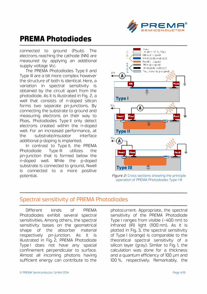
PREMA Photodiodesconnected to ground (Psub). The electrons reaching the cathode (NN) are measured by applying an additional supply voltage Vcc.
The PREMA Photodiodes Type II and Type III are a bit more complex however the structure of both is identical. Here, a variation in spectral sensitivity is obtained by the circuit apart from the photodiode. As it is illustrated in Fig. 2, a well that consists of n-doped silicon forms two separate pn-junctions. By connecting the substrate to ground and measuring electrons on their way to Pbas, Photodiodes Type II only detect electrons created within the n-doped well. For an increased performance, at the substrate/insulator interface additional p-doping is implanted.
In contrast to Type II, the PREMA Photodiode Type III utilizes the pn-junction that is formed below the n-doped well. While the p-doped substrate is connected to ground, Nwell is connected to a more positive potential. Figure 2: Cross sections showing the principle
operation of PREMA Photodiodes Type I-III
Spectral sensitivity of PREMA Photodiodes
Different kinds of PREMA Photodiodes exhibit several spectral sensitivities. Among others, the spectral sensitivity bases on the geometrical shape of the absorber material respectively pn-junction. As it is illustrated in Fig. 2, PREMA Photodiode Type I does not have any spacial confinement perpendicular to surface. Almost all incoming photons having sufficient energy can contribute to the
photocurrent. Appropriate, the spectral sensitivity of the PREMA Photodiode Type I ranges from visible (~400 nm) to infrared (IR) light (1100 nm). As it is plotted in Fig. 3, the spectral sensitivity of Type I (orange) is comparable to the theoretical spectral sensitivity of a silicon layer (gray). Similar to Fig. 1, the calculation was done for a thickness and a quantum efficiency of 100 µm and 100 %, respectively. Remarkably, the
© PREMA Semiconductor GmbH 2014 Page 4/16

PREMA Photodiodesactual performance of the PREMA Photodiode Type I that is not limited in depth is comparable to the achievable maximum sensitivity.
Figure 3: Spectral sensitivities for PREMA Photodiodes Type I - III (see Fig. 2). While Type I
(orange) is comparable to the theoretical maximum (gray), Type II (blue) and Type III (black) are designed for selected spectral
sensitivities for visible and IR light.
Besides the performance of Type I that collects all incoming photons, varied spectral sensitivities can be obtained by PREMA Photodiodes Type II and Type III. By the utilization of the pn-junction within and below the n-doped well (see Fig. 2), preferred spectral sensitivities in the visible and the IR range can be selected, respectively. It can be extracted from Fig. 3 that the photocurrent detected by Type II (blue) originates from the upper silicon layers. Thus, the Photodiode Type II is not very sensitive for infrared light.
In contrast, the PREMA Photodiode Type III detects a photocurrent that originates from deeper layers. Here, parts of the visible light are already absorbed and only residual photons can contribute to the photocurrent. Therefore, Type III (black) is mainly sensitive for infrared light (Fig. 3).
Remarkably, the sum of spectral sensitivities corresponding to Type II and Type III are roughly about the spectral sensitivity of Type I.
Furthermore, using proper external wiring, Type II and Type III can be combined to determine roughly the ratio of visible and IR light to the total radiation. Potentially, various information can be received, by measuring the relation of visible to IR light over time.
In contrast to the calculation (gray), measured spectral sensitivities exhibit an additional peak structure. These periodically arranged maxima originate from interference effects in the insulation layer that is deposited directly on the silicon during the chip manufacturing process. Light enters this insulation layer (dielectric layer) and is subsequently reflected at the insulation/silicon interface and at the surface of the insulation layer. According to the superposition of reflected beams, maxima and minima in the spectral sensitivity (Fig. 3) occur due to destructive and constructive interference. Because interference depends on optical path length to wave length ratio, these peaks shift with thickness variations of the insulation layer.
© PREMA Semiconductor GmbH 2014 Page 5/16

PREMA Photodiodes
Effects of insulation layer and anti-reflective coating
PREMA PHOTODIODE TYPE I
In the following two opportunities are presented to get rid of the interference effect. For the PREMA Photodiode Type I, varied spectral sensitivities measured with dielectric layer (blue), without dielectric layer (black) and with an anti-reflective coating (orange) are shown in Fig. 4. If the dielectric layer is omitted, the total amount of photons entering the photodiode is decreased by the larger discontinuity in the index of refraction from air to the silicon. But in addition to the decreased spectral sensitivity, the interference effects are disappeared.
Enhanced performance with increased spectral sensitivity is obtained by using an anti-reflective coating ARC (orange). Here, an additional layer with adapted thickness and index of refraction is deposited on the silicon. Thus, a spectral sensitivity can be obtained that comes close to the theoretical maximum (see Fig. 3). For PREMA Photodiodes Type I, photons with wavelengths from 400 to 1100 nm can be detected.
Based on calculations for spectral sensitivities (Fig. 1), a detailed calculation (gray) has been done for the photodiode with an anti-reflective coating ARC (orange). Here, information about specific dimensions of the pn-junction, electron diffusion and the effect of the anti-reflective coating ARC has been added to a quantum efficiency of 100 %.
Figure 4: Spectral sensitivities are shown for the PREMA Photodiode Type I with dielectric
layer (blue), uncoated (black) and anti-reflective coating ARC (orange). For the latter, an
additional calculation (gray) is given.
© PREMA Semiconductor GmbH 2014 Page 6/16

PREMA Photodiodes
PREMA PHOTODIODES TYPE II ANDTYPE III
Similar measurements were done with PREMA Photodiodes Type II (Fig. 5) and Type III (Fig. 6). By removing the insulation layer (dielectric layer) and leaving the silicon uncoated, the interference effects vanish as well. For both kinds a reduction in spectral sensitivity is detected. But applying the detailed calculation demonstrates the conclusive performance of PREMA Photodiodes. For selected wavelengths, anti-reflective coatings enable a performance close to theoretical limit. Here, maxima in spectral sensitivities are obtained at about 530 and 880 nm for PREMA Photodiodes Type II and Type III, respectively.
Figure 5: Spectral sensitivities for the PREMA Photodiodes Type II with dielectric layer (blue), uncoated (black) and a calculation for the anti-
reflective coating (orange).
In the present case the n-doped well of Type II and Type III (see Fig. 2) is implanted the furthest into the silicon substrate. Thus, by implanting the well less deep, varied spectral sensitivities can be generated. Especially for PREMA Photodiodes Type II (Fig. 5), the spectral sensitivity of the luminous efficiency function for scotopic vision can easily be received. Here, the spectral sensitivity ranges from 400 to 600 nm.
Figure 6: Spectral sensitivities for the PREMA Photodiodes Type III with dielectric layer (blue), uncoated (black) and a calculation for the anti-
reflective coating (orange).
© PREMA Semiconductor GmbH 2014 Page 7/16

PREMA Photodiodes
Impact of transparent packaging on PREMA Photodiodes Type I
Figure 7: The spectral currents of 10 encapsulated PREMA Photodiodes Type I are
measured. Beside an average value (blue), the standard deviation (gray) is given.
Etching the dielectric layer and the deposition of an anti-reflective coating are extra processing steps that increase the costs of manufacturing. As it is shown in Fig. 7 the interference effects are already reduced by packaging in a transparent encapsulation. For many application, especially for those measuring a spectral range, the photodiodes satisfy without specific post-processing steps. Fig. 7 shows the variation of 10 different encapsulated photodiodes coming from the same wafer. While the mean spectral sensitivity of 10 photodiodes is shown in blue, the standard deviation for individual photodiodes at each wavelength is given in gray.
Sample applications for photodiodes
Figure 8: The capacity utilization of an assembly line measured by a light barrier.
Photodiodes are used to detect electromagnetic radiation. In a most simple case valuable information can already be obtained by an on/off state. Therefore, a measured intensity (photocurrent) goes above or below a certain threshold value. Schematically, an example is illustrated in Fig. 8. A light barrier consisting of a LED and photodiode are mounted to measure the position of bottles on an assembly line. According to the direction of motion the optical beam path is positioned perpendicular. Thus, the
© PREMA Semiconductor GmbH 2014 Page 8/16

PREMA Photodiodesphotodiode measures a lower intensity if a bottle passes. In bright rooms the background intensity can be decreased by appropriate shielding. If that is not sufficient, IR radiation can be utilized. Here, PREMA Photodiode Type III is well-suited for.
Equally operating systems can be found in elevators to check the absence
of people at the doors while closing them. For simplification, LED and photodiode are located at one side. This can be realized by a reflector at the other side of the door. Thus, the beam passes the door twice.
The complexity of monitoring can be increased by an array of LEDs and photodiodes. As the simplified image in Fig. 9 illustrates, the shape of items can be obtained by light intensities (photocurrents) measured at different positions. In the present case only photodiode 1 and 2 do not measure any change in intensity while the bottle passes perpendicular to the image plane. Occasionally, a certain intensity profile can be used to check the accuracy of a manufacturing process. In Fig. 9, for a filled bottle an intensity profile is shown exemplary.
Here, PREMA Semiconductor GmbH can reveal its strength of combining photodiodes with application specific integrated circuits (ASICs). For example, an ASIC can be used in addition to evaluate photocurrents, measured by several photodiodes, to output a single voltage. Based on requirements of applications, output voltages can have any characteristics. In addition, ASICs can be integrated for controlling and to operate further manufacturing processes.
Figure 9: The shape of items can be determined by light curtains.
© PREMA Semiconductor GmbH 2014 Page 9/16
PREMA PhotodiodesThe triangulation method can be
used to measure height differences. In this method, stray light that comes from the surface of a sample is analyzed. As it is schematically shown in Fig. 10, a horizontal shift (black arror) of the reflective surface causes a variation of the focus point (red arror). This variation can be detected by a photodiode with spatial resolution.
Appropriate to the Dual-Photodiode PR5001 (shown at front page), in the present example two separate photodiodes can resolve two different heights. Based on request several photodiodes can closely be aligned next to each other. Finally, a suitable analysis can be done by an integrated circuit.
Figure 10: Triangulation method to measure height differences
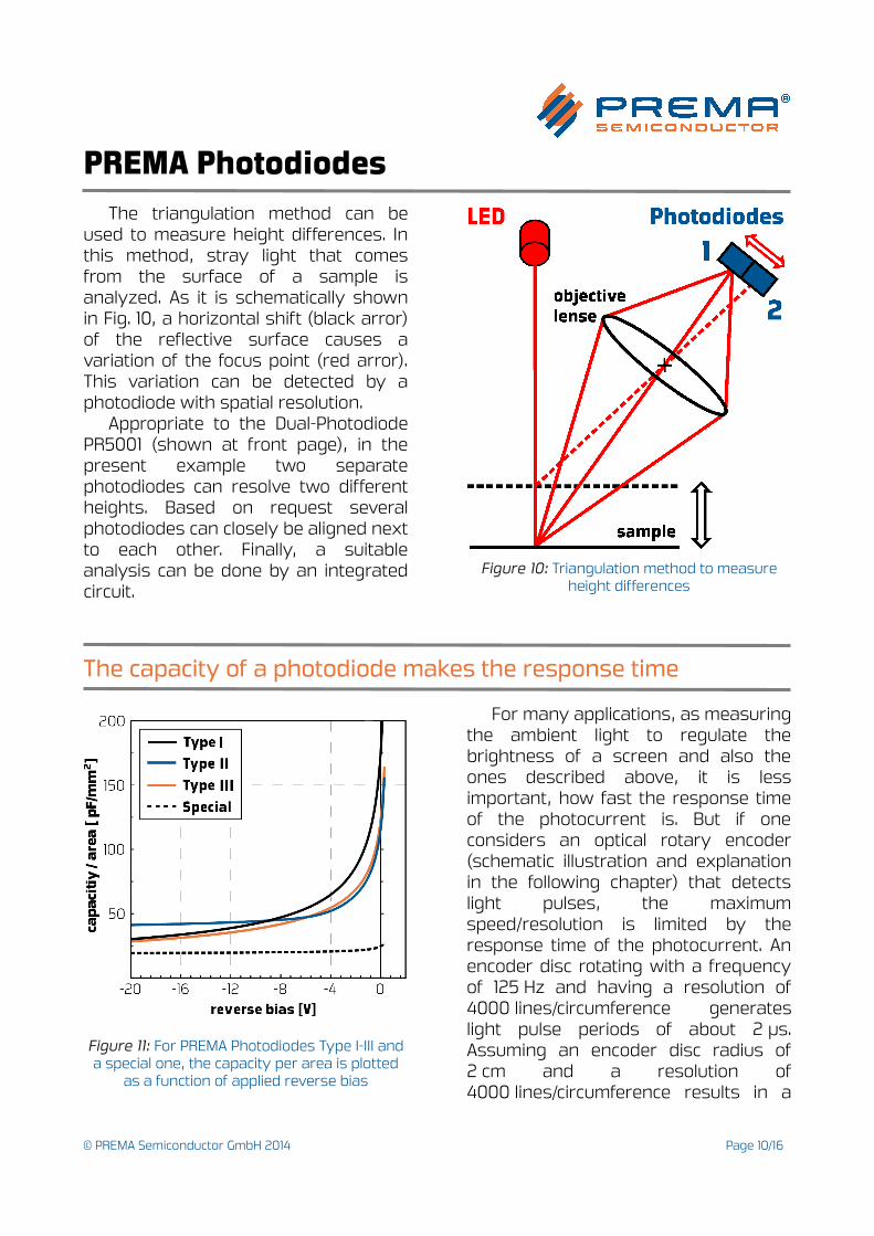
The capacity of a photodiode makes the response time
Figure 11: For PREMA Photodiodes Type I-III and a special one, the capacity per area is plotted
as a function of applied reverse bias
For many applications, as measuring the ambient light to regulate the brightness of a screen and also the ones described above, it is less important, how fast the response time of the photocurrent is. But if one considers an optical rotary encoder (schematic illustration and explanation in the following chapter) that detects light pulses, the maximum speed/resolution is limited by the response time of the photocurrent. An encoder disc rotating with a frequency of 125 Hz and having a resolution of 4000 lines/circumference generates light pulse periods of about 2 µs. Assuming an encoder disc radius of 2 cm and a resolution of 4000 lines/circumference results in a
© PREMA Semiconductor GmbH 2014 Page 10/16

PREMA Photodiodesperiodicity of 16 µm. The example shows that neither the resolution on the encoder disc nor the frequency are extremely high, but the response time of an applied photodiode already becomes relevant. The discussed demand is even enhanced by rise and fall times within the pulse periods that are appreciated to be as steep as possible.
A useful approach to reduce the capacity of a photodiode is to apply a reverse bias that causes a wider depletion zone. For PREMA Photodiodes Type I-III, the dependence of capacity on reverse bias voltage is quantitatively shown in Fig. 11. A significant reduction can be obtained if a reverse bias voltage > 4 V is applied. For higher voltages, the capacity barely decreases further. Noticeable, the slope for Type II (blue) is even flatter. This can be explained by the limited size of the depletion zone in the photodiode.
A further approach to reduce the capacity of a photodiode is the optimization of the lateral layout of the pn-junction. As it is shown in Fig. 11, PREMA has developed a particular kind of photodiode. A 'special' PREMA Photodiode (dashed line) exhibits a lower capacity than the PREMA Photodiodes Type I-III (solid lines). Remarkably, at zero applied voltage, the capacity is reduced by a factor of ten. Simultaneously, the spectral sensitivity of the adapted pn-junction is only reduced by about 20 %. According to requirements of particular applications, the reduction in spectral sensitivity might be negligible while the gain in response time is indispensable.
Figure 12: Effect of reverse bias (caption) on spectral sensitivity of PREMA Photodiode Type I
As it has been initially introduced, the capacity of a photodiode can be reduced by a reverse bias. For the PREMA Photodiode Type I the effect of reverse bias on the spectral sensitivity is illustrated in Fig. 12. It can be seen that there isn't any significant deviation for applied voltages of 0 V, 1 V or 10 V.
Using PREMA Photodiodes Type I-III, the maximum spectral sensitivity can be preserved while the capacity is intensively reduced for applied reverse voltages > 4 V. For high speed applications with further reduced capacity, especially at low applied reverse bias, a 'special' PREMA Photodiode with low capacity needs to be considered.
© PREMA Semiconductor GmbH 2014 Page 11/16

PREMA Photodiodes
IR remote control receiver
Figure 13: Block diagram of a IR remote control receiver
The block diagram of a typical application for the 'special' PREMA Photodiode with a low capacity is illustrated in Fig. 13. Often IR remote controls send modulated signals with wavelength of 900 nm and carrier frequencies of 36 kHz or 38 kHz. Thus, spectral sensitivity as well as raise an fall times of the 'special' PREMA Photodiode are sufficient for application.
After the infrared light is absorbed by the photodiode, a transimpedance amplifier (TIA) is used to convert the photocurrent into a voltage signal that is subsequently amplified by a variable gain amplifier (VGA). A bandpass filter is applied to get rid of noise. Finally, the integrator and the hysteresis comparator demodulate and digitize the signal, respectively.
Due to its ability of manufacturing integrated circuits, PREMA Semiconductor GmbH perfectly understands how to integrate a photodiode and the corresponding circuit into one chip. Furthermore, the integration of additional sensor functions can easily be implemented for controlling devices.
© PREMA Semiconductor GmbH 2014 Page 12/16

PREMA Photodiodes
Photodiodes applied in optical encoders
Figure 14: Schematic illustration of an optical encoder offered by PREMA
Especially, in automation technology measuring motion of mechanically moving parts is of importance for a smooth and precise operation. Among others, rotation as well as linear motion can be detected optically. Schematically, the principle is illustrated in Fig. 14. Here, a LED, an encoder disk, a reticle and a
photodiode (chip) are used to generate a signal according to the motion. While the encoder disc rotates, the light is subsequently transmitted or blocked by periodically arranged pattern. To enhance the performance of an optical encoder, a reticle is placed close to either the photodiode or the LED. Properly chosen pattern enable a high resolution and the recognition of the direction of rotation.
Due to the general knowledge that PREMA has gained in the field of application specific integrated circuits (ASICs), further processing of signals can be done, based on customer needs. Next to a simple amplification, PREMA ASICs that can be integrated into the photodiode can operate other devises as motors or LEDs.As it is denoted in Fig. 14, LED, encoder disk, reticle and PCP are offered as well. The resolution that your product requires can be easily obtained by the pattern at the encoder disc. The pattern can be individually adapted. Ito safe money, a special feature enables a fast mounting of the encoder in your product.
© PREMA Semiconductor GmbH 2014 Page 13/16

PREMA Photodiodes
Sensitivity boosted by PREMA Phototransistors
Figure 15: Schematic assembly of a PREMA Phototransistor
Ultra-high sensitivity is reached with the PREMA Phototransitor. With a further pn-junction (Fig. 15) between the n-doped Emitter and the n-doped collector, a npn-transistor is formed. But instead of controlling the collector-emitter current by the basis-emitter current, the conduction from collector to emitter is stimulated by light irradiation. The current gain is typically around 100 and can be extracted from the comparison of Fig. 16 and Fig. 5 which shows the spectral sensitivity of PREMA Photodiode Type II. This makes a phototransistor rather feasible for applications with reduced illuminance as sensitive motion detectors, light barriers or optocouplers.Due to their sensitivity and their ability to isolate electric circuits from another, optocouplers are implemented in electronic devices. In a simplified manner, the assembly is illustrated in Fig. 17. Encapsulated in one package a photodiode and a phototransistor are used to transmit or to amplify a signal. Due to the cut-off frequency of
phototransistors, caused by raise and fall times of a few µs, frequencies higher than several kHz can not be transferred anymore.
Figure 16: Spectral sensitivity of a PREMA Phototransistor
Figure 17: Schematic assembly of an optocoupler
© PREMA Semiconductor GmbH 2014 Page 14/16

PREMA Photodiodes
Summary
PREMA Photodiodes and Transistors can meet diverse requirements as variable applicability, high sensitivity, low response times, low capacities and adjusted sensitivities.
Simple transparent dielectric layers that can be delivered with convenient prices already fulfill most applications. For measuring an integrated light spectrum as adjusting the brightness of screens, occurring interference effects do not matter. This interference effects do not matter either if ON or OFF states are detected, as for example in photo-electric barriers. Here, varied intensities of signals can be adapted.
If PREMA Photodiodes are intended to be used in an environment with monochromatic light in combination with a high demand on measuring intensities quantitatively, PREMA Photodiodes with anti-reflective coatings ARC have to be applied.
Further applications, requiring fast response times or ultra-high sensitivities, can be excellently achieved by special photodiodes a with low capacity and by phototransistors, respectively.
For open questions, do not hesitate to contact PREMA Semiconductor GmbH. We would like to assist you to find the ideal device for your needs.
Crucially, PREMA Semiconductor GmbH is well-experienced in designing ASIC-Products for more than 20 years. Thus, combining Photodiodes with costumer adapted ICs can lead to innovative products that give your company a competitive advantage ahead of the field. Due to the PREMA HighVoltage Implantation process, a copy protection for your product is already included.
© PREMA Semiconductor GmbH 2014 Page 15/16

PREMA Photodiodes
DisclaimerInformation provided by PREMA is believed to be accurate and correct. However, no responsibility is assumed by PREMA for its use, nor for any infringements of patents or other rights of third parties which may result from its use. PREMA reserves the right at any time without notice to change circuitry and specifications.
Life Support PolicyPREMA Semiconductors products are not authorized for use as critical components in life support devices or systems without the express written approval of PREMA Semiconductor. As used herein:1. Life support devices or systems are devices or systems which, (a) are intended for surgical implant into the body, or (b) support or sustain life, and whose failure to perform when properly used in accordance with instructions for use provided in the labeling, can be reasonably expected to result in a significant injury to the user.2. A critical component is any component of a life support device or system whose failure to perform can be reasonably expected to cause the failure of the life support device or system, or to affect its safety or effectiveness.
PREMA Semiconductor GmbHRobert-Bosch-Str. 655129 Mainz GermanyPhone: +49-6131-5062-0Fax: +49-6131-5062-220Email: [email protected] Web site: www.prema.com
© PREMA Semiconductor GmbH 2014 Page 16/16