Embed Size (px)
Citation preview

RDA5981A IEEE 802.11b/g/n MCU WIFI Rev1.1
The information contained herein is the exclusive property of RDA and shall not be distributed, reproduced, or disclosed in whole or in part without prior written permission of RDA. Page 1 of 16
PRELIMINARY DATA SHEET
Revision: 1.1
Release date: 17 May 2017
RDA5981A IEEE802.11b/g/n MCU WIFI
RDA5981A IEEE 802.11b/g/n MCU WIFI Rev1.1
The information contained herein is the exclusive property of RDA and shall not be distributed, reproduced, or disclosed in whole or in part without prior written permission of RDA. Page 2 of 16
1. General Description
RDA5981A is a low power MCU with IEEE802.11b/g/n MAC/PHY/radio integrated into one chip. TCP/IP protocols along with SSL are included, providing improved link robustness, extended range, and increased performance. For the highest integration level, the required board space has been minimized and customer cost has been reduced. Manufacturers can easily and fast integrate RDA5981A on their product to enable a rapid time to market.
RDA5981A uses a compact 5×5mm² QFN package, 0.4mm pitch QFN-40.
1.1 WLAN Features
CMOS single-chip fully-integrated radio, PHY and MAC
2.4GHz IEEE 802.11b/g/n Internal PA, LNA Data rates up to 150Mbps with 20/40
MHz bandwidth Dynamic TX power saving Low power listen mode
Fast AGC control Support WPS, WMM Support WPA, WPA2, WEP, TKIP,
CCMP Support STA, softAP, P2P, STA+softAp,
STA+P2P Support A-MPDU, A-MSDU, HT-BA Light Weight TCP/IP protocol
1.2 MCU Features
Integrated ARM-CM4 MCU, Maximum clock Frequency 160MHz
Integrated MPU and mbed uvisor supported to isolate security domains
Up to 352KBytes internal sram for WIFI protocol and application developments
SPI / UART / USB2.0 interface allows simple interfacing to host device
UART with an AT command set Integrated hardware crypto accelerator
AES/RSA Integrated true random number generator
(TRNG) and CRC accelerator
Support external psram interface Integrated 8Mbit SPI flash in package Integrated a bunch of configurable
GPIOs with external level/edge trigger/wakeup
Integrated UART×2/I2S×2/I2C×1 /PWM×8/SPI×4/SDMMC×1/USB2.0×1
Integrated 2 channels application ADC Integrated watchdog and low power
timer 16×16 bits eFuse configuration Support freeRTOS/mbedOS5.1

RDA5981A IEEE 802.11b/g/n MCU WIFI Rev1.1
The information contained herein is the exclusive property of RDA and shall not be distributed, reproduced, or disclosed in whole or in part without prior written permission of RDA. Page 3 of 16
1.3 Applications
IOT devices Smart home Wi-Fi speaker/home audio Smart watch

RDA5981A IEEE 802.11b/g/n MCU WIFI Rev1.1
The information contained herein is the exclusive property of RDA and shall not be distributed, reproduced, or disclosed in whole or in part without prior written permission of RDA. Page 4 of 16
2. Block Description
Figure2-1 RDA5981A Block Diagram
RDA5981A IEEE 802.11b/g/n MCU WIFI Rev1.1
The information contained herein is the exclusive property of RDA and shall not be distributed, reproduced, or disclosed in whole or in part without prior written permission of RDA. Page 5 of 16
3. Functional Description
3.1 Memory System
RDA5981A integrates ROM, internal RAM and SPI nor flash to provide applications with a variety of memory requirements.
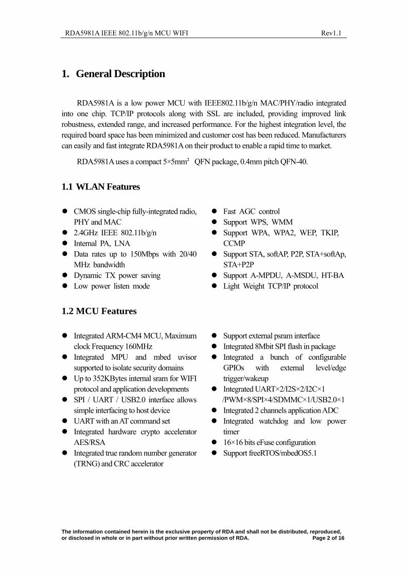
3.1.1 Memory Map
Table 3-1 RDA5981A Memory Map
Component Address Range Size comments
MEMORY
BOOT_ROM 0x0000_0000-0x0000_FFFF 64K
I_SRAM 0x0010_0000-0x0011_FFFF 128K
D_SRAM 0x0018_0000-0x0018_FFFF 64K
PSRAM 0x1000_0000-0x13FF_EFFF data 64M
FLASH 0x1400_0000-0x147F_FFFF FLASH data 8M
I-cache 0x1800_0000-0x1FFF_FFFF I-cache
LOGIC
SCU 0x40000000-0x40000FFF 4K
GPIO 0x40001000-0x40001FFF 4K
TIMER 0x40002000-0x40002FFF 4K
I2C_master 0x40003000-0x40003FFF 4K
PWM 0x40004000-0x40004FFF 4K
PSRAM_CFG 0x40005000-0x40005FFF 4K
SDMMC 0x40006000-0x40006FFF 4K
I2C 0x40010000-0x40010FFF 4K
UART1 0x40012000-0x40012FFF 4K
AHB_EXIF 0x40013000-0x40013FFF 4K
WIFI_PA 0x40020000-0x40021FFF 8K
WIFI_CE 0x40022000-0x40022FFF 4K
WLAN_MON 0x40024000-0x40027FFF 20K
SDIO 0x40030000-0x40030FFF 4K
USB 0x40031000-0x40031FFF 4K
MEMC0 0x40100000-0x4017FFFF 512k
UART2 0x40180000-0x40180FFF 4K
DMA_CFG 0x40181000-0x40181FFF 4K

RDA5981A IEEE 802.11b/g/n MCU WIFI Rev1.1
The information contained herein is the exclusive property of RDA and shall not be distributed, reproduced, or disclosed in whole or in part without prior written permission of RDA. Page 6 of 16
3.1.2 Internal ROM
RDA5981A integrates internal ROM to provide basic functions: eFuse functions USB/SPI interface initialization MCU/Wi-Fi mode initialization
3.1.3 Internal RAM
RDA5981A integrates: 96K Bytes SRAM for user 32K Bytes icache
3.1.4 SPI Nor FLASH
RDA5981A supports standard SPI mode and SPI-Quad mode and integrated 8Mbit flash in package.
3.2 GPIO Characteristics
Table 3-2 GPIO Configurable Function Summary Table

RDA5981A IEEE 802.11b/g/n MCU WIFI Rev1.1
The information contained herein is the exclusive property of RDA and shall not be distributed, reproduced, or disclosed in whole or in part without prior written permission of RDA. Page 7 of 16
3.3 UART Interface Characteristics
RDA5981A supports 2 UARTs with configurable baud rate from 1200bps to 4Mbps.
3.4 I2S Interface Characteristics
RDA5981A supports 2 I2S interface; the I2S master BCLK supports 96/192/384/512/ 44.1/88.2KHz. The interface supports 16/32 bit per channel, the data format can be configured as 16/20/24bit per channel or decided by software (up to 24bit per channel).
3.5 I2C Interface Characteristics
RDA5981A supports 1 I2C standard interface. It supports master or slave I2C operation and 3 standard speed modes: 1. Standard mode (<100Kb/s) 2. Fast mode (<400Kb/s) 3. High-speed mode (<3.4Mb/s)
3.6 PWM Interface Characteristics
RDA5981A supports 8 PWM interfaces. Period and Duty of PWM is programmable. The Duty of PWM/PWT/PWL can be flexible configured between 0~100. The accurate of duty is 1%.The period are programmable, the software can select different clock to product long Period.
Table 3-3 PWM Period & Duty
Name Number Duty Period
PWM 4 1~100% 5us-256s Standard PWM
PWT 1 1~100% 5us-4s Standard PWM
LPG 1 <25% <2s The wave has a short pull
up in a long period
PWL 2 1~100% - The wave is non-periodic,
use for screen background
light
3.7 SPI Interface Characteristics
RDA5981A supports 4 SPI interfaces, master only. The SPI clock rate is

RDA5981A IEEE 802.11b/g/n MCU WIFI Rev1.1
The information contained herein is the exclusive property of RDA and shall not be distributed, reproduced, or disclosed in whole or in part without prior written permission of RDA. Page 8 of 16
programmable and up to 20MHz. The data length can be configured by the software, the max data length is 64bit.
3.8 SDMMC Interface Characteristics
RDA5981A supports 1 SDMMC interface.
3.9 USB Interface Characteristics
RDA5981A supports USB interface.

RDA5981A IEEE 802.11b/g/n MCU WIFI Rev1.1
The information contained herein is the exclusive property of RDA and shall not be distributed, reproduced, or disclosed in whole or in part without prior written permission of RDA. Page 9 of 16
4. WLAN Section Electrical Characteristics
Table 4-1 DC Electrical Specification (Recommended Operation Conditions)
SYMBOL DESCRIPTION MIN TYP MAX UNIT
VBAT Supply Voltage from battery or LDO 3.3 4.0 5.0 V
Tamb Ambient Temperature -20 27 +70 ℃
VIL CMOS Low Level Input Voltage 0 0.3*VIO V
VIH CMOS High Level Input Voltage 0.7*VIO VIO V
VTH CMOS Threshold Voltage 0.5*VIO V
Table 4-2 DC Electrical Specification (Absolute Maximum Ratings)
SYMBOL DESCRIPTION MIN TYP MAX UNIT
IIN Input Current -10 +10 mA
VIN Input Voltage -0.3 VIO+0.3 V
Vlna LNA Input Level +10 dBm
RDA5981A IEEE 802.11b/g/n MCU WIFI Rev1.1
The information contained herein is the exclusive property of RDA and shall not be distributed, reproduced, or disclosed in whole or in part without prior written permission of RDA. Page 10 of 16
5. PINS Description
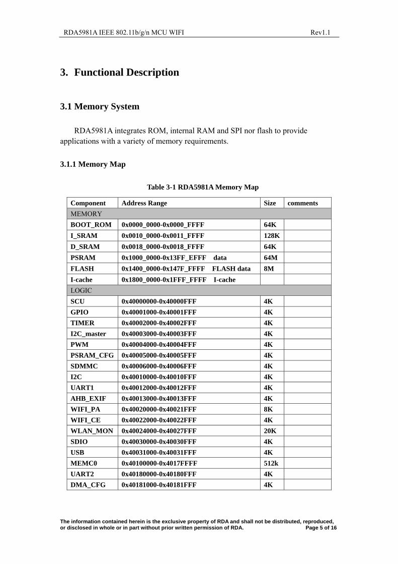
Table 5-1 Pin Types
Pin Type Description I/O Digital input/output I Digital input O Digital output A,I Analog input A,O Analog output A,I/O Analog input/output PWR Power GND Ground
Table 5-2 RDA5981A Pins Description
PIN NO. TYPE DESCRIPTION VBAT 1 PWR buck power supply SW_GND 2 GND buck ground
SW_Buck 3 PWR Switching node of buck
VA18 4 PWR 1.8V power output LX_Buck 5 PWR Switching output VD11 6 PWR 1.1V power output GPIO9 7 I/O General purpose input/output V_CORE 8 PWR digital core power in USB_DN 9 I/O USB negative signal USB_DP 10 I/O USB positive signal GPADC0 11 I/O General purpose ADC GPIO7 12 I/O General purpose input/output GPIO8 13 I/O General purpose input/output GPIO5 14 I/O General purpose input/output GPIO4 15 I/O General purpose input/output UART_TX 16 I/O UART_TX PDN 17 I Power Down signal of the chip AVDD33_PAD 18 PWR 3.3V PA driver power in AVDD33_PA 19 PWR 3.3V PA power in RFIO 20 A,I/O WIFI transmitter output/receiver input GPIO1 21 I/O General purpose input/output GPIO2 22 I/O General purpose input/output GPIO3 23 I/O General purpose input/output UART_RX 24 I/O UART_RX AVDD_RF 25 PWR 1.8V RF power in AVDD_CLK 26 PWR 1.8V clock power in XIN 27 A,I 26M crystal input XTAL 28 A,O 26M crystal output GPIO13 29 I/O General purpose input/output GPIO12 30 I/O General purpose input/output GPIO25 31 I/O General purpose input/output GPIO24 32 I/O General purpose input/output

RDA5981A IEEE 802.11b/g/n MCU WIFI Rev1.1
The information contained herein is the exclusive property of RDA and shall not be distributed, reproduced, or disclosed in whole or in part without prior written permission of RDA. Page 11 of 16
GPIO23 33 I/O General purpose input/output
GPIO22 34 I/O General purpose input/output
GPIO21 35 I/O General purpose input/output
GPIO0 36 I/O General purpose input/output
VIO_LDO 37 I/O I/O power output VIO 38 PWR I/O power supply LDO33 39 PWR 3.3V LDO output VBAT 40 PWR power supply
RDA5981A IEEE 802.11b/g/n MCU WIFI Rev1.1
The information contained herein is the exclusive property of RDA and shall not be distributed, reproduced, or disclosed in whole or in part without prior written permission of RDA.
Page 12 of 16
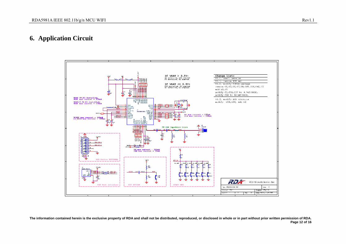
6. Application Circuit
RDA5981A IEEE 802.11b/g/n MCU WIFI Rev1.1
The information contained herein is the exclusive property of RDA and shall not be distributed, reproduced, or disclosed in whole or in part without prior written permission of RDA.
Page 13 of 16
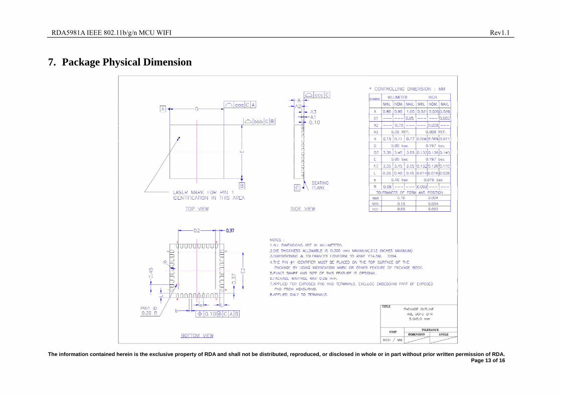
7. Package Physical Dimension

RDA5981A IEEE 802.11b/g/n MCU WIFI Rev1.1
The information contained herein is the exclusive property of RDA and shall not be distributed, reproduced, or disclosed in whole or in part without prior written permission of RDA. Page 14 of 16
8. Recommended Reflow Profile
Figure.8-1 Classification Reflow Profile
Table 8-1 Classification Reflow Profiles
Profile Feature Sn-Pb Eutectic Assembly Pb-Free Assembly
Average Ramp-Up Rate 3 ℃/second max. 3 ℃/second max.
(TSmax to Tp)
Preheat
-Temperature Min (Tsmin) 100 ℃ 150 ℃
-Temperature Max (Tsmax) 100 ℃ 200 ℃
-Time (tsmin to tsmax) 60-120 seconds 60-180 seconds
Time maintained above:
-Temperature (TL) 183 ℃ 217℃
-Time (tL) 60-150seconds 60-150 seconds
Peak /Classification See Table 8-2 See Table 8-3
Temperature(Tp)
Time within 5 oC of actual Peak 10-30 seconds 20-40 seconds
Temperature (tp)
Ramp-Down Rate 6 ℃/second max. 6 ℃/seconds max.
Time 25 oC to Peak 6 minutes max. 8 minutes max.
Temperature
RDA5981A IEEE 802.11b/g/n MCU WIFI Rev1.1
The information contained herein is the exclusive property of RDA and shall not be distributed, reproduced, or disclosed in whole or in part without prior written permission of RDA. Page 15 of 16
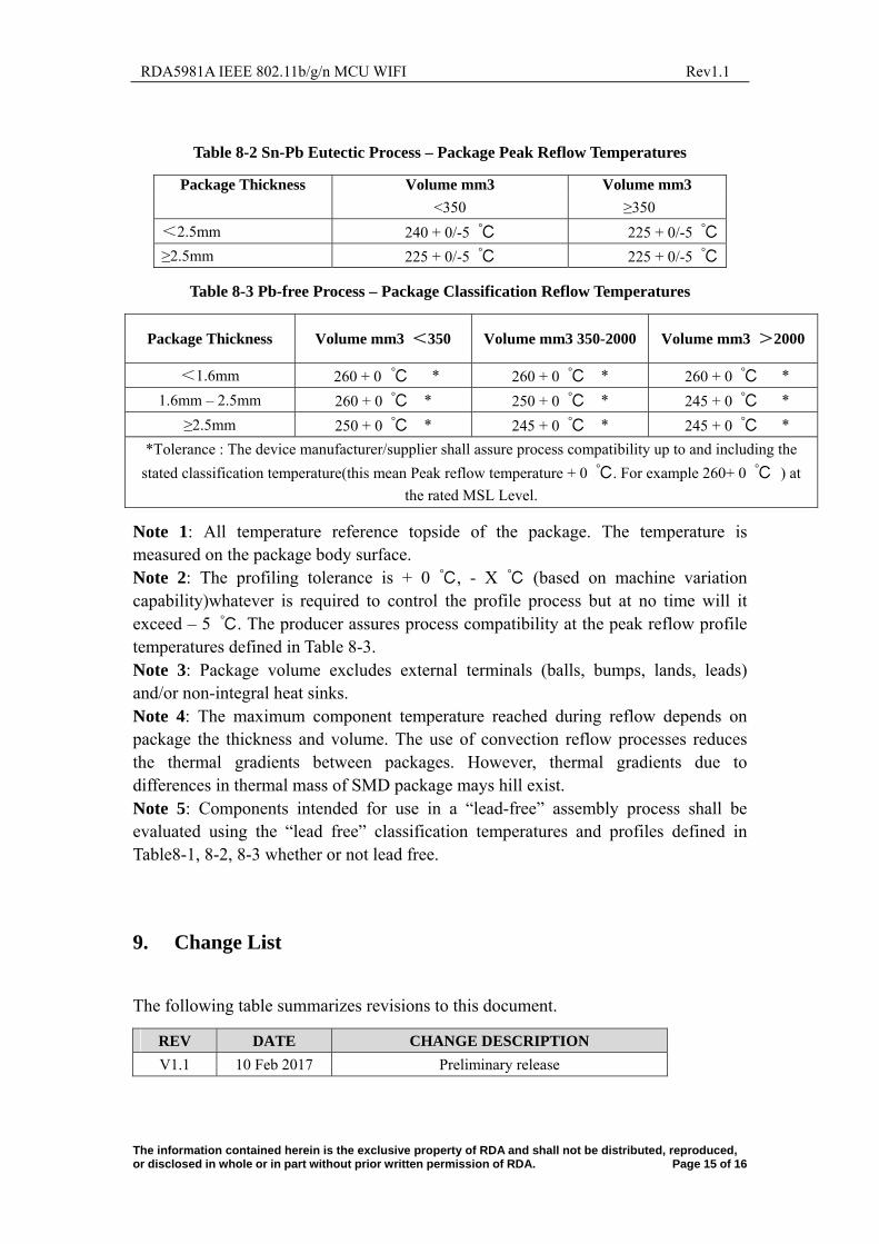
Table 8-2 Sn-Pb Eutectic Process – Package Peak Reflow Temperatures
Package Thickness Volume mm3 Volume mm3
<350 ≥350
<2.5mm 240 + 0/-5 ℃ 225 + 0/-5 ℃
≥2.5mm 225 + 0/-5 ℃ 225 + 0/-5 ℃
Table 8-3 Pb-free Process – Package Classification Reflow Temperatures
Package Thickness Volume mm3 <350 Volume mm3 350-2000 Volume mm3 >2000
<1.6mm 260 + 0 ℃ * 260 + 0 ℃ * 260 + 0 ℃ *
1.6mm – 2.5mm 260 + 0 ℃ * 250 + 0 ℃ * 245 + 0 ℃ *
≥2.5mm 250 + 0 ℃ * 245 + 0 ℃ * 245 + 0 ℃ *
*Tolerance : The device manufacturer/supplier shall assure process compatibility up to and including the
stated classification temperature(this mean Peak reflow temperature + 0 ℃. For example 260+ 0 ℃ ) at
the rated MSL Level.
Note 1: All temperature reference topside of the package. The temperature is measured on the package body surface. Note 2: The profiling tolerance is + 0 ℃, - X ℃ (based on machine variation capability)whatever is required to control the profile process but at no time will it exceed – 5 ℃. The producer assures process compatibility at the peak reflow profile temperatures defined in Table 8-3. Note 3: Package volume excludes external terminals (balls, bumps, lands, leads) and/or non-integral heat sinks. Note 4: The maximum component temperature reached during reflow depends on package the thickness and volume. The use of convection reflow processes reduces the thermal gradients between packages. However, thermal gradients due to differences in thermal mass of SMD package mays hill exist. Note 5: Components intended for use in a “lead-free” assembly process shall be evaluated using the “lead free” classification temperatures and profiles defined in Table8-1, 8-2, 8-3 whether or not lead free.
9. Change List
The following table summarizes revisions to this document.
REV DATE CHANGE DESCRIPTION
V1.1 10 Feb 2017 Preliminary release
RD
The ior dis
10.
polyther
11.
prec
12.
assuno rbe achanthis RDAlife Cop
For WebMaiRDATel:Fax
DA5981A IEE
information cosclosed in who
RoHS Co
The produybrominatedrefore is con
ESD Pr
ESD protcautions are
Disclaim
The informumes no relreliability foat the user’snge withoutinformatio
A Microelesupport dev
pyright@20
technical qbsite: www.ilbox: info@A Microele +86-10-58
x: +86-10-58
EE 802.11b/g
ontained hereinole or in part w
ompliant
uct does nod biphenylnsidered Ro
recautions
tection circe required.
mer
mation proviability for
for the use os own risk. t notice on tn describedctronics dovices or sys16 RDA M
questions an.rdamicro.co
@rdamicro.cctronics (Be
8286588 8286599
/n MCU WIF
n is the exclusiwithout prior wr
ot contain lls (PBB)
oHS complia
s
cuitry is co
vided here iinaccuracieof this inforSpecificatiothe purpose
d herein shoes not authotems. icroelectron
nd additionaom com eijing), Inc.
FI
ve property of ritten permissio
lead, mercuor polybroant.
ontended in
is believed es and omisrmation andons describee of improviould not be iorize or war
nics Inc. All
al informatio
.
f RDA and shalon of RDA.
ury, cadmiuominated d
n this dev
to be reliabsions. RDAd all such ined and conting the desigimplied or grrant any R
l rights rese
on about RD
l not be distrib
um, hexavaldiphenyl e
ice, but sp
ble; RDA MA Microelect
nformation ained here agn and perfgranted for
RDA product
erved
DA Microel
Rev1
buted, reproduc Page 16
alent chromethers (PBD
pecial hand
Microelectrotronics assushould ent
are subjecteformance. Aany third pts for use in
lectronics In
1.1
ced, 6 of 16
mium, DE),
dling
onics umes irely ed to
All of party. n the
nc.:


![INTEGRATED AMPLIFIER Audio Analogue Puccini Anniversary · 8 DSD [HFN May ’16] – her Easy Living set with Joe Pass [88.2kHz/24-bit from HDTracks; Pablo 0888072328419] – I was](https://img.dokumen.tips/doc/110x75/5f601ebf175776140c0905f4/integrated-amplifier-audio-analogue-puccini-anniversary-8-dsd-hfn-may-a16-a.jpg)