Embed Size (px)
Citation preview

Structured Hardware Design
New revised 6L 1A edition.
DJ Greaves
April 28, 1998
1 Building Blocks for Digital Electronics.2 Clocking and Synchronous FSM Combination.3 Technology, Speed, Power and Gate Delays.4 Hardware and Software Design Partition.5 Modular Design and Design Partition.6 Further Circuit Structures.
Further copies of these notes can be printed from the Web page on the front cover. Copyright forthese notes belongs to DJ Greaves. c 1998.
Preface
This is the new, revised, six lecture Structured Hardware Design course for 1A. The materialcovered is di�erent from the older 1B course. Some of the material previously covered is now inthe new 1B 8L ECAD course.
Bibliography (Book list)
Books related to the course, in approximate order of importance, are:
W.Ditch. `Microelectronic Systems, A practical approach.' Edward Arnold. The �nal chapterswith details of the Z80 and 6502 are not relevant to this course.
Floyd. `Digital Fundamentals' Prentice Hall International.
T.J. Stoneham. `Digital Logic Techniques' Chapman and Hall. This is a basic book and relatesmore to the previous course on Digital Electronics.
Randy H Katz. `Contemporary logic design.' Benjamin Cummings ISBN 0 8053 2703 7
Texas Instruments. `System 74 Series Logic Family.' Texas Instruments.
Old�eld, Gray, Kean, Dorf. `Field Programmable Gate Arrays.' New York; Chichester: Wiley,c1995.
L.J. Herbst `Integrated circuit engineering: establishing a foundation.' Oxford University Press,c1996.
1

Glossary of jargon and acronyms
Here are some acronyms:
ALU Arithemetic and logic unit.ASIC Application speci�c integrated circuit.
BICMOS A process with both CMOS and bipolar transistors on one die.CAD Computer aided design.CAE Computer aided engineering.CAM Computer aided manufacture.CLB Con�gurable logic block.CRC Cyclic redundancy check (added to end of a data frame).CMOS Complementary metal oxide of silicon.DRAM Dynamic random access memory.DMA Direct memory access.DSP Digital signal processor/ing.EDO Extended Data Out for DRAMS.ECL Emitter coupled logic.EMC Electromagnetic compatibility.EMI Electromagnetic ingress or i(m)missions (sic).FET Field e�ect transistor.FSM Finite state machine.FPGA Field programmable gate array.GaAs Gallium Arsenide.HDL Hardware description language.IEEE Institure of electrical and electronic engineers.IPR Intellectual Property Rights.JTAG Joint technical advisory groupLSI Large scale integration (say about 5000 gates, 10000 transistors).LCA Logic cell array.MCM Multi-chip module.MSI Medium scale integration (i.e. the larger ttl devices).NRE Non recurring engineering costs. i.e paid once per design.OTP One-time programmablePAL Programmable array logic.PIO Programmed Input and Output.PCB Printed ciruit board.PLL Phase-locked loop.PIN Personal identi�cation number.RTL Register transfer level.SRAM Static RAM.SIMM Single in-line memory module.SSI Small scale integration (i.e. about 4 gates on a chip).TTL Transistor-transistor logic.UART Universal asynchronous recevier and transmitter.Verilog An HDL language in wide use (not an acronym).VHDL VHSIC Hardware Description LanguageVHSIC Very High Speed Integrated CircuitVNL Verilog netlist.VCO Voltage controlled oscillator.VLSI Very large scale integration (big chips).XNF Xilinx netlist format.
2

The Boss
Marketing Sales Software Hardware Miscellaneous
The Board
ChipDesignTeam
PCBDesignTeam
FoundryPCB
Assembly
Production
- Accounts- Personnel- Lawyers- Hangerson
ProgrammersPublic
Relations
InventoryStock Control
Salesmen
Advertising
TestingProduct
Prototypes
Figure 1: Structure of a small company with hardware products that use its own hardware, softwareand chips.
Introduction
A good hardware design works the �rst time. A structured approach to its design is required ifthe system is complicated. Simulation of the system behaviour before fabrication is also vital tohelp get it right. As Figure 1 shows, the �nal product relies on successful interworking betweencustom chips and the other parts on the circuit boards, together with the software.
Most designs today are held in a database which contains details of custom circuits, printed circuitboards, other chips, software, part numbers and so on. The database can help automate everypart of the design process, except for the initial design decisions. These decisions de�ne the basicstructure of the product and they are what this course is about.
To create a new hardware design, as with software, it is important to use a top-down approach,starting with an accurate capture of the requirements speci�cation and then decomposing thesystem into modules. As with software, the module must have well-de�ned functions and well-de�ned interfaces and tghe modules must be suitable for individual testing. However, two bigdi�erences are 1. that the modules in hardware are often made of di�erent technology from oneanother, and 2. that the desireability of using pre-existing modules is much greater.
3

Broadsideregister
N N
Clock
QD
D
Clock
D
D
D
Q0
Q1
Q2
Q(N-1)
D0
D1
D2
D(N-1)
Figure 2: A broadside register: schematic symbol and internal structure.
1 Building Blocks in Digital Electronics.
This section introduces a number of building blocks that are frequently used in hardware designs.In times gone by, these were refered to MSI (medium scale integration) and LSI (large scaleintegration) subsystems. Today, many of these blocks rarely exist as separate components: insteadthey are placed inside custom (or semi-custom) application-speci�c, integrated circuits (ASICs).
1.1 Busses and Broadside Components.
A bus is a number of signals that operate in parallel to carry a binary number. In the schematics,a thicker line is used, and the number next to the slash is the number of signals in the bus.
Figure 2 demonstrates the concept of a broadside component, in this case, a broadside set ofD-types. To form a broadside component, the building block is instantiated a number of timeswith the data inputs and outputs connected to the member lines of input and output busses. Thecontrol connections are paralleled and driven from a single external source. A broadside set of ip- ops is a register.
Figure 3 shows the schematic and a suitable circuit implementation for a broadside, two-inputmultiplexor. Most systems will regard a two input multiplexor as a fundamental building blockand implement it at the transistor level, rather than from gates.
Figure 4 shows the schematic symbol for a dual-port register �le. This device internally containsa number of broadside registers and multiplexors, but they are grouped into the �le for convenientaccess. Such a �le is a key part of all computers. The illustrated dual-port �le has two readingports and one writing port, so might be considered a tripple-ported �le. On the positive edge of theclock, the data on the write port is stored in the addressed register. For reading, at any time, likean SRAM, the read address may be changed and the output data will change shortly afterwards.
Exercise: Sketch the circuitry that would turn a collection of standard broadside registers into adual-port �le. You will have to use one of the clock enabling techniques de�ned in section 2.
4

MUX2N
NN
Select
DT
DFY
Select
Y0
Y1
Y(N-1)
DT0
DF0
DT1
DF1
DT(N-1)
DF(N-1)
Figure 3: An N-bit broadside, two-to-one multiplexor.
Write Address
Data in Data out A
clock
N N
A
Read Address B
A
Read Address A
A
Data out B
N
Figure 4: Dual port register �le.
5

The ROM takes A address bits named A0 to A<A-1> and produces datawords of N bits wide. For example, if A=5 and D=8 then the ROMcontains 2**5 which is 32 locations of 8 bits each. The address linesare called A0, A1, A2, A3, A4 and the data lines D0, D1, ... D7
Address In
Data Out
Enable Input(active low)
Valid dataHigh-ZHigh-Z
The ROM’s outputs are high impedance unless the enable inputis asserted (low). After the enable is low the
output drivers turn on. When the address has been stablesufficiently long, valid data from that address comes out.
The ROM contentsare placed inside during
manufacture or fieldprogramming.
Data Out
Address In
Enable Input(active low)
E
Addr
Data
NA
ROMPROM
orEPROM
Access Time
Ouput Turnon Time
Figure 5: Read Only Memory (ROM).
1.2 Read Only Memories
Figure 5 shows the logic symbol for a read only memory (ROM). The contents are non-volatile andare placed in the ROM during manufacture using a fabrication mask or with a special programmingstep in the �eld. The techniques for storing �eld programmed information are:
� W-Sn fuse: One time programmable by melting selected fuses. This is an old technologywhich is not very reliable or dense. When used for ROM gives a PROM.
� Antifuse: One time programmable, high density process. Used on one contemporary familyof FPGAs. Not used in ROMs today.
� Floating gate technology with ultraviolet erase. A static electrical charge is stored on the oating gate and is put there using a supervoltage that causes tunneling or other breakdownsin the insulator. Discharge is achieved using intense ultraviolet illumination to make thecharge leak away. When used for a ROM, gives an EPROM.
A varient on EPROM is an OTP-EPROM (one-time-programmable) which the same devicepackaged in a windowless package at much lower cost.
� Electrically reprogrammable oating gate devices. Again charge is stored on the gate, butelectrical techniques used for programming can be applied for erasing. Used widely in personalorganisers and (Flash) memory cards and in most modern PAL devices. Often, erase ofindividual bits is impossible: only block erase is supported.
Mask programmed ROMs of several megabytes may cost sub 50 pence each in quantities of tens ofthousands. Flash memory may be more than 100 times more expensive. The choice of which tech-
6

nology to use depends on the number of units that are going to be made and the expected numberof reprogramming cycles required. There is always a testing problem with one time programmabledevices!
1.3 RAM memories
Figure 6 shows a random access memory or RAM. It is as equally random access as a ROM, so isa misnomer. RAM is normally volatile, meaning it loses its contents when power is disconnected.Static RAM (SRAM) normally uses one ip- op per bit stored. A transparent latch su�ces, so itis not as complicated as having a D-type per bit. A possible internal structure for an SRAM isshown in Figure 7. However this would lead to a long, skinny chip. In practice, a square array ofstorage elements is used, meaning that the on-chip tri-state bus is much wider than the externaldata bus. The on-chip bus will have width approximately equal to the square root of the numberof bits stored in the device. Modern SRAM devices have an access time of 20 nanoseconds andhave capacities of about half a megabyte. Price is about six pounds per megabyte, but dependsgreatly on the access time required. Second-level cache chips for PCs are SRAMs and produced inhigh volume, so are currently a good way to purchase SRAM, even for other designs or uses.
A property of the SRAM, shared with the ROM, is that there is no clock and, during read, theoutput is essentially a combinatorial logic function of the address input value.
When writing, the address must not change and the data present on the data pins at the backedge of the (active low) write pulse is the data actually written.
Figure 8 shows the schematic symbol for a dynamic RAM. DRAMs store their data not in ip- ops, but in small capacitors. The value stored leaks away over time unless refreshed. It is alsodestroyed by readout: after readout, the device always writes back the value internally, removingthe job from external circuitry, but meaning that the external logic must not start a new cycleimmediately. Therefore the cycle time and access times of DRAM are di�erent. Typically, today,DRAM cycle and access times are 60 and 120 nanoseconds and capacity is 2 to 4 megabyte.
All DRAMs are accessed by applying the address in two halves. First a row address is presentedand RAS taken low, then a column address is applied, and CAS is taken low. These row andcolumn addresses typically correspond to the actual physical topology of the rectangular array ofbits on the device. In external view, some DRAMs are one bit wide and others are four.
DRAM is much cheaper than SRAM owing to the smaller silicon area needed per bit. Smallerpackages are also possible, owing to the multiplexed address bus.
Refresh cycles do not transfer data in or out of the chip, but must be done su�ciently often anyway.A typical speci�cation is that 512 refresh cycles are executed every 4 milliseconds. Since DRAMconsumes most of its power when being refreshed, a designer who puts all of the refresh cycles inone batch at the end of every 4 millisecond period makes the design of power supplies much moredi�cult.
Modern EDO (extended data out) DRAMs guarantee that the data will be valid on the output fora period after CAS is deasserted, thereby easing system timings and helping the designer.
DRAMs are often packed on SIMMs (single in line memory modules). Capcities of SIMMs arearound 16 to 32 Mbyte with prices of tens of pounds per SIMM.
High performance systems today use synchronous DRAMs (SDRAM) which incluce broadsideregisters on the address or data connects. This gives a pipeline delay (section 2.4) but allows fasteroperation.
Exercise: When would you use SRAM and when DRAM ?
Exercise: Sketch the circuitry that could be put around a bank of DRAM to make it appear like anSRAM with a single, non-multiplexed address bus and similar control signals. What shortcomingshave you made ?
7

Address In
Data Bus
Enable Input(active low)
Valid dataHigh-ZHigh-Z
Read Cycle - Like the ROM
Write Cycle - Data stored internally
Read or writemode select
Address In
Data Bus
Enable Input(active low)
Data must be validhere to be stored.
High-Z
High-Z
Read or writemode select
Data In and Out
Address In
Enable Input(active low)
E
Addr
Data
N
A
RAMR/WbRead or write
mode select
Figure 6: Read and Write Memory (RAM).
8

GD GD GD GD GD GDData
Address Input
Binary to unary decoder
WE*
CE*
outputenable
G
QD
Transparent latchschematic symbol
D
G
Q
Transparent latch implemented from gates.
Figure 7: Schematic and possible implementation of a transparent latch and a naive implementationof an SRAM using broadside transparent latches.
9
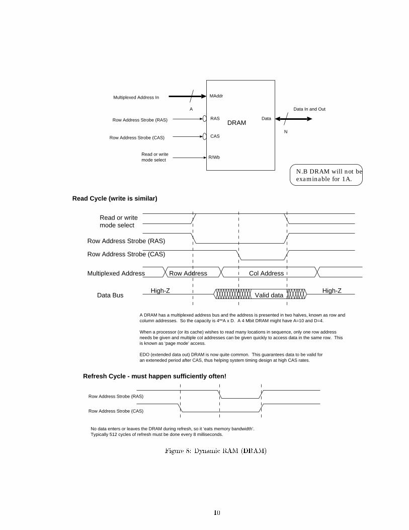
Refresh Cycle - must happen sufficiently often!
A DRAM has a multiplexed address bus and the address is presented in two halves, known as row andcolumn addresses. So the capacity is 4**A x D. A 4 Mbit DRAM might have A=10 and D=4.
When a processor (or its cache) wishes to read many locations in sequence, only one row addressneeds be given and multiple col addresses can be given quickly to access data in the same row. Thisis known as ‘page mode’ access.
EDO (extended data out) DRAM is now quite common. This guarantees data to be valid foran exteneded period after CAS, thus helping system timing design at high CAS rates.
Multiplexed Address
Data Bus Valid dataHigh-ZHigh-Z
Read Cycle (write is similar)
Read or writemode select
Row Address Col Address
Row Address Strobe (RAS)
Row Address Strobe (CAS)
Row Address Strobe (RAS)
Row Address Strobe (CAS)
No data enters or leaves the DRAM during refresh, so it ‘eats memory bandwidth’.Typically 512 cycles of refresh must be done every 8 milliseconds.
Data In and Out
Multiplexed Address In
Row Address Strobe (RAS) RAS
MAddr
Data
N
A
DRAM
R/WbRead or writemode select
Row Address Strobe (CAS) CAS
N.B DRAM will not beexaminable for 1A.
Figure 8: Dynamic RAM (DRAM).
10

33pF
Ground
33pF
1M
Figure 9: A crystal oscillator clock source.
Ground
C
R
Figure 10: An RC oscillator clock source.
1.4 Miscellaneous Components
Figure 9 shows a circuit frequently used as a clock source. A carefully cut slither of quartz crystalis used as the timing reference. Quartz is pizoelectric, so can be made to change shape by applyingan AC signal across metal coatings applied to its sides. Also, as it changes shape, it generatesan equivalent electrical signal. Since the speed of sound in quartz is very high, a slice about 100microns thick will resonate at several MHz. The details of the circuit are beyond the scope of thiscourse, but su�ce to note that the sine waves generated by the crystal become good quality squarewaves, suitable for use as a clock, after passing through a few inverters. A crystal might cost onepound to add to a design, but is accurate to about 50 parts per million in frequency, so is highlyuseful.
Figure 10 shows a cheaper circuit that serves as a clock when accuracies of only a few percent areneeded. The �rst inverted must be a special Schmidt inverter with abrubt switching and hysteresisfor the circuit to work. The capacitor is the only component that is hard to make on an integratedcircuit, so a single pin on the device serves to connect the external capacitor. The crystal oscillatoralways needs two pins.
Figure 11 shows the typical arrangement of clock distribution inside a large, modern IC. The clockis actually provided from a lower-frequency external reference and multiplied up internally with aphase-locked loop. Skew in the delivery to the various parts of the device is minimised by using abalanced clock distribution tree. Inverters are used instead of bu�ers to minimise pulse shrinkage(duty-cycle distortion).
Figure 12 shows a circuit that is often used to generate a reset signal when a system is switched on.When power is applied, the capcitor is initially discharged, so has zero volts across it. Thereforethe output is a logic one. After a while, the resistor charges the capacitor such that the input tothe invertor crosses the switching threshold of the Schmidt input and the output from the circuit
11

VCO
Clock distribution tree
66 MHz
33 MHz
Divide 2
Externalclockinput
PLL Circuit
Figure 11: Typical clock multiplication and distribution system for a large IC.
Ground
C
R
Reset output
Supply
Figure 12: A circuit often used as a power up reset.
12

Ground
R
Control input
High Voltage Supply
EMFdiode
Powertransistor
Figure 13: A typical structure used to drive a heavy current or high-voltage load.
is deasserted. Typical delay times used are about half a second, which is long enough for the powersupply to become stable and for oscillators to settle down. The diode discharges the capacitorinto the supply rail when power is removed. On most devices, a reset switch is also �tted, whichdischarges the capacitor when pressed, therefore starting the device as from power up.
Figure 13 shows a typical structure used to drive a high power load from a logic signal. Thesemiconductor processing used to fabricate logic devices may be too expensive to waste on largetransistors or may not be able to tolerate the higher voltages required to control the load. There-fore, external driver transistors in individual packages or in power driver ICs are used. Typicalapplications are motor, loudspeaker, solenoid, relay, and print head driving.
Figure 14 shows the circuit typically used to get a clean signal out of a mechanical switch. Insuch a switch, when one contact hits another, it bounces o� with a supersonic ping, which meansthat the circuit is made and broken a few thousand times for each switching operation executed.Using a two-pole switch and an RS latch formed from a pair of cross-coupled NAND gates, a cleanoutput is generated. The systems works on the basis that the �rst time the commuting contacthits the stator contact, the latch changes state, and stays there until the switch is moved all theway back to the other side, where the reverse happens.
1.5 ALU and ALU circuits
The arithmetic and logic unit (ALU) is a fundamental block of all computers: it is the basisof the integer execution unit. Figure 15 shows the normal schematic for an ALU. The ALU iscombinatorial, but is shown connected to a ag register, which does have a clock input. For adetailed example, look at the 74181 in the System 74 databook.
The illustrated ALU has two N-bit inputs and a 4 bit function code input. The output is also N-bit.The function code determines what function of the two inputs is computed. Typical functions areadd, add with carry, bitwise AND and OR, subtract and identity functions of the two inputs. Theinstruction set for the ARM microprocessor contains 16 data manipulation instructions which area good example of the 16 most useful functions that an ALU can perform.
Like all combinatorial logic functions, the ALU is guaranteed to compute its output within a �xedtime interval from the last input change. The value of this delay is typically dependent on the carrychain speed inside the ALU and it will set the maximul clock frequency of a simple microprocessor.
Question: Suggest why ALU's typically only support addition and subtraction as arithmetic op-erations and not multiplication or division ?
13

A
B
Output
Output
A
B
Gnd
+5Volt supply rail
PullupResistors
Bounces
Switch
Figure 14: A debouncer circuit for a two-pole switch.
Function Code4
N
N
N
Carry In
ALU
A-input
B-input
Output
C
N
Z
V
Flags Clock
Flags register
Figure 15: Schematic symbol for an ALU, connected to a ags register.
14
FunctionCode
4
8
Carry In
8 bitALU
A-input
B-input
Output
4 bitcounter
Register file16 registers
of 8 bits
4
A
8
D
Carry Out
QDin
8
B
A
Clock source
FUNCTION GEN
Zerodetect
8
FUNCTION GEN
for F code
for A input
Figure 16: Example structure using an ALU and register �le.
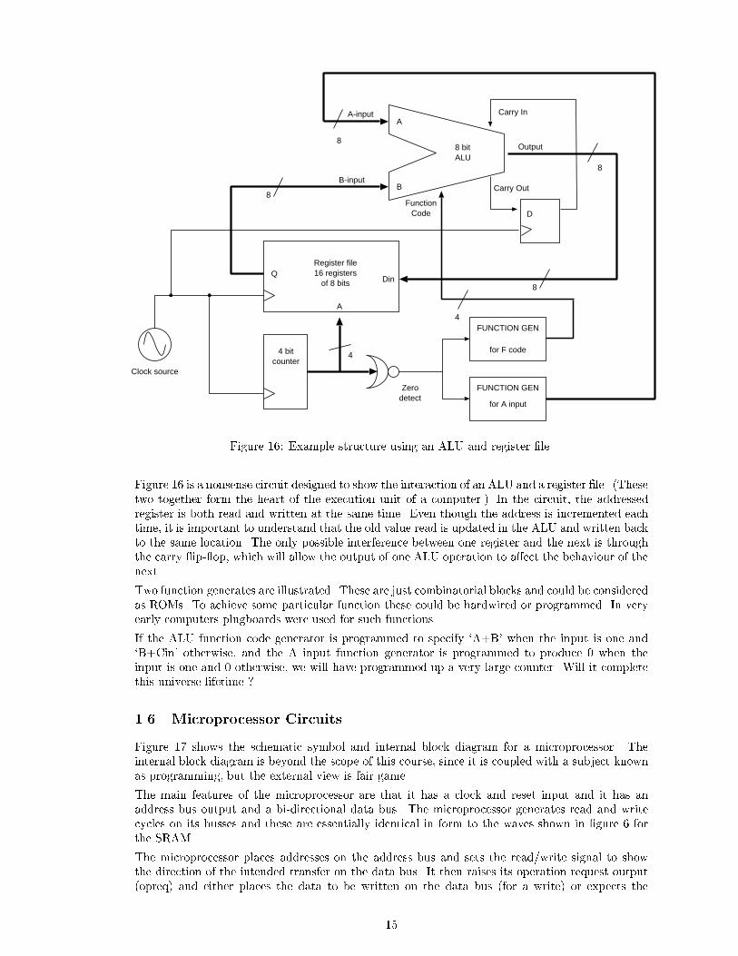
Figure 16 is a nonsense circuit designed to show the interaction of an ALU and a register �le. (Thesetwo together form the heart of the execution unit of a computer.) In the circuit, the addressedregister is both read and written at the same time. Even though the address is incremented eachtime, it is important to understand that the old value read is updated in the ALU and written backto the same location. The only possible interference between one register and the next is throughthe carry ip- op, which will allow the output of one ALU operation to a�ect the behaviour of thenext.
Two function generates are illustrated. These are just combinatorial blocks and could be consideredas ROMs. To achieve some particular function these could be hardwired or programmed. In veryearly computers plugboards were used for such functions.
If the ALU function code generator is programmed to specify `A+B' when the input is one and`B+Cin' otherwise, and the A input function generator is programmed to produce 0 when theinput is one and 0 otherwise, we will have programmed up a very large counter. Will it completethis universe lifetime ?
1.6 Microprocessor Circuits
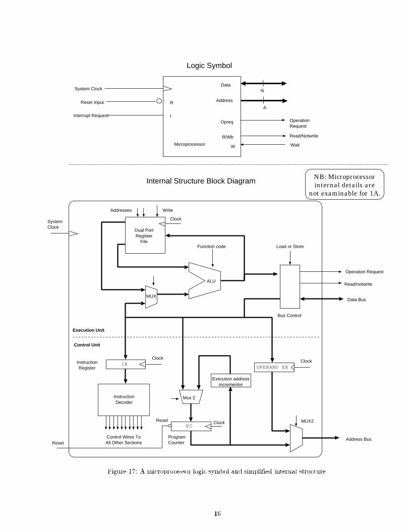
Figure 17 shows the schematic symbol and internal block diagram for a microprocessor. Theinternal block diagram is beyond the scope of this course, since it is coupled with a subject knownas programming, but the external view is fair game.
The main features of the microprocessor are that it has a clock and reset input and it has anaddress bus output and a bi-directional data bus. The microprocessor generates read and writecycles on its busses and these are essentially identical in form to the waves shown in �gure 6 forthe SRAM.
The microprocessor places addresses on the address bus and sets the read/write signal to showthe direction of the intended transfer on the data bus. It then raises its operation request output(opreq) and either places the data to be written on the data bus (for a write) or expects the
15
Logic Symbol
Internal Structure Block Diagram
Address
DataN
A
System Clock
Reset Input
Interrupt RequestOperationRequest
Read/Notwrite
Wait
I
W
R/Wb
Opreq
R
Microprocessor
Operation Request
Read/notwrite
Data Bus
Address Bus
Bus Control
Clock
ALU
MUX
Addresses
Dual PortRegister
File
Write
Execution Unit
Control Unit
InstructionRegister
InstructionDecoder
Control Wires ToAll Other Sections
Mux 2
ProgramCounter
Execution addressincrementor
Clock
ClockClock
MUX2
Function code Load or Store
NB: Microprocessorinternal details are
not examinable for 1A.
System Clock
ResetPC
Reset
OPERAND EAIR
Figure 17: A microprocessor logic symbol and simpli�ed internal structure.
16

D Q
GND
VCCBroadside latch
Broadsidetri-state
Microprocessor
D0
D1
D2
Part of data bus
Part of address bus
A12
A13
A14
A15
R/Wbar
OPREQ
Pullup resistors
Light emitting diodes(LEDs)
Write to leds
Read from switches
D3
D4
D5 Switches
Figure 18: Example of memory address decode and simple LED and switch interfacing for pro-grammed IO (PIO) to a microprocessor.
addressed device to drive the data bus with its information (for a read).
Figure 18 shows how to connect some LEDs and switches to a microprocessor for simple pro-grammed input and output. Only the low order data bits are used, so when reading from theswitches, random values may appear on the higher order bits. Conversley, when writing to theLED registers, the higher order bits are ignored.
Exercise: If the address bus is 16 bits, how many addresses are consumed by the switches andleds. If the data bus is 8 bits, what percentage of addressable bits have been wasted and is this asensible design ?
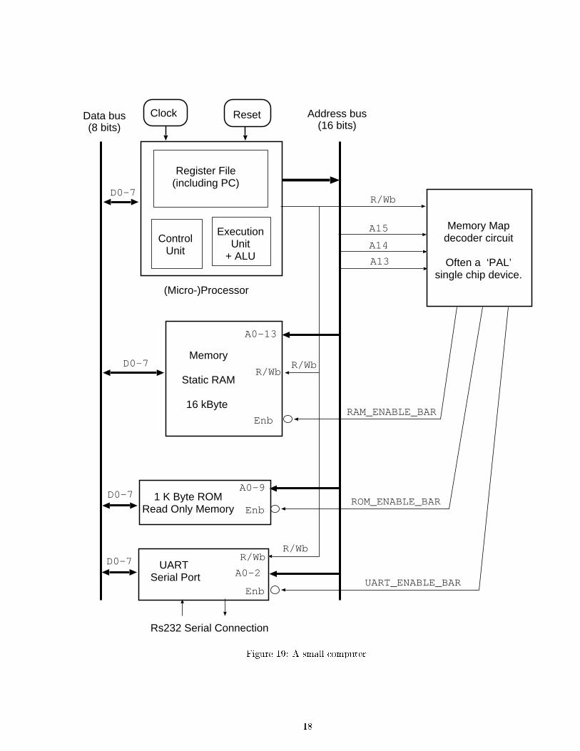
Figure 19 is the circuit of small, microprocessor based computer. The microprocessor can address216 locations of eight bits (65536 bytes) and some of these are �lled in with devices.
Exercise: What would happen if the microprocessor tried to write to the read only memory ?
Exercise: Figure 20 shows the signals involved in a parallel port, as frequently used to connectprinters to computers. The basic operation is that the master places a byte of data on the databus and then strobes the strobe signal low until acknowledge is asserted by the device. The mastermust not present a new byte to the printer while the printer has put busy high. Design the parallelport interface logic by drawing on the ideas shown in �gure 18. To do this, it is su�cient if thebusy signal appears to the processor like one of the switch inputs and the data output is ratherlike eight LEDs. Considering that the processor really does not care about the acknowledge signal
17
ControlUnit
ExecutionUnit
+ ALU
Memory
Static RAM
16 kByte
UART Serial Port
Address bus(16 bits)
Data bus(8 bits)
(Micro-)Processor
Rs232 Serial Connection
Register File(including PC)
D0-7
D0-7
D0-7
Clock Reset
R/Wb
Memory Mapdecoder circuit
Often a ‘PAL’single chip device.
A15
A14
A13
R/WbR/Wb
A0-13
Enb
Enb
Enb
1 K Byte ROMRead Only Memory
A0-9
A0-2
R/WbR/Wb
ROM_ENABLE_BAR
UART_ENABLE_BAR
RAM_ENABLE_BAR
D0-7
Figure 19: A small computer.
18

Address
Data
device select/cs
Strobe
Read/Writebarr/wbar
Acknowledge
Parallel Data
Busy
D25 Parallel (Centronix) Port
Strobe_bar
Acknowledge
Parallel Data
Busy
Valid Data For Transfer To Peripheral Device
Ready for next data
Parallel Port Interface Logic
Figure 20: PC or Centronics Parallel Printer Port.
or when the strobe signal is deasserted, you might care to use an RS latch to help the processorgenerate the strobe signal.
19

FSM
Clock
Mealy Outputs
Inputs
D
Clock
D
D
D
Q0
Q1
Q2
Moore Outputs
LOOP-FREE COMBINATORIAL LOGIC BLOCK
I0
I1
I(M-1)
M
I2
CURRENT STATE FEEDBACK
STATE FLOPS
LOOP-FREE COMBINATORIAL LOGIC BLOCK
LOOP-FREE COMBINATORIAL LOGIC BLOCK
Figure 21: Canonical synchronous, �nite-state machine.
2 Clocking and Synchronous FSM Combination.
This section looks at aspects of clock signals and considers the how, when and why of multipleclocks in a system. The decisions relating to clocks are fundamental to any hardware design andare normally taken very early in the process.
2.1 Finite State Machines.
Figure 21 shows the schematic symbol and canonical circuit for a �nite-state machine. It is amantra among mature hardware designers to consider everything as a collection of �nite-statemachines. Beginner hardware designers tend not to have this approach, and instead think nothingof treating the clock input to a ip- op as suitable for wiring to anything convenient. They do notget far like this, since all CAD tools, design techniques and formal methods will stop providingany help and circut bugs will creep up everywhere. (An exception is certain licensed asynchronoushardware designers, like Dr Simon Moore, who often don't even have clocks in their circuits.)
20
Clock
Data in
D Q oiutputQ
Q oiutput
Data in
Clock
Hold time
Propagation delay
Setup time
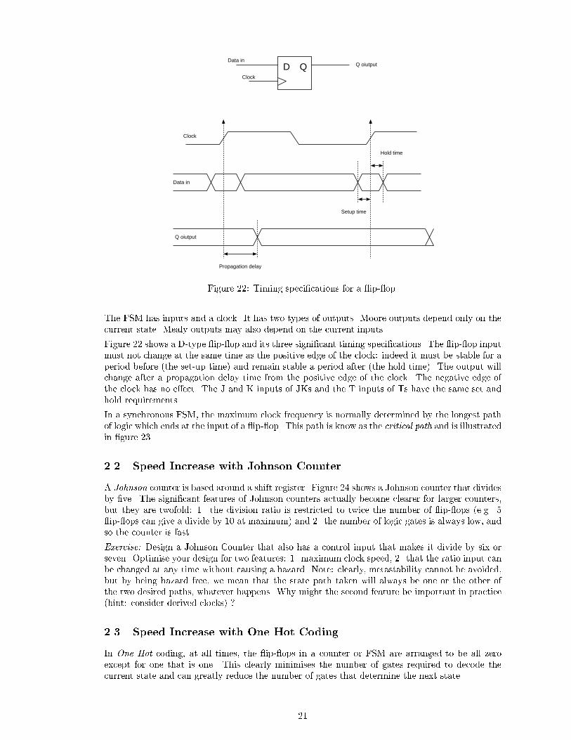
Figure 22: Timing speci�cations for a ip- op.
The FSM has inputs and a clock. It has two types of outputs. Moore outputs depend only on thecurrent state. Mealy outputs may also depend on the current inputs.
Figure 22 shows a D-type ip- op and its three signi�cant timing speci�cations. The ip- op inputmust not change at the same time as the positive edge of the clock: indeed it must be stable for aperiod before (the set-up time) and remain stable a period after (the hold time). The output willchange after a propagation delay time from the positive edge of the clock. The negative edge ofthe clock has no e�ect. The J and K inputs of JKs and the T inputs of Ts have the same set andhold requirements.
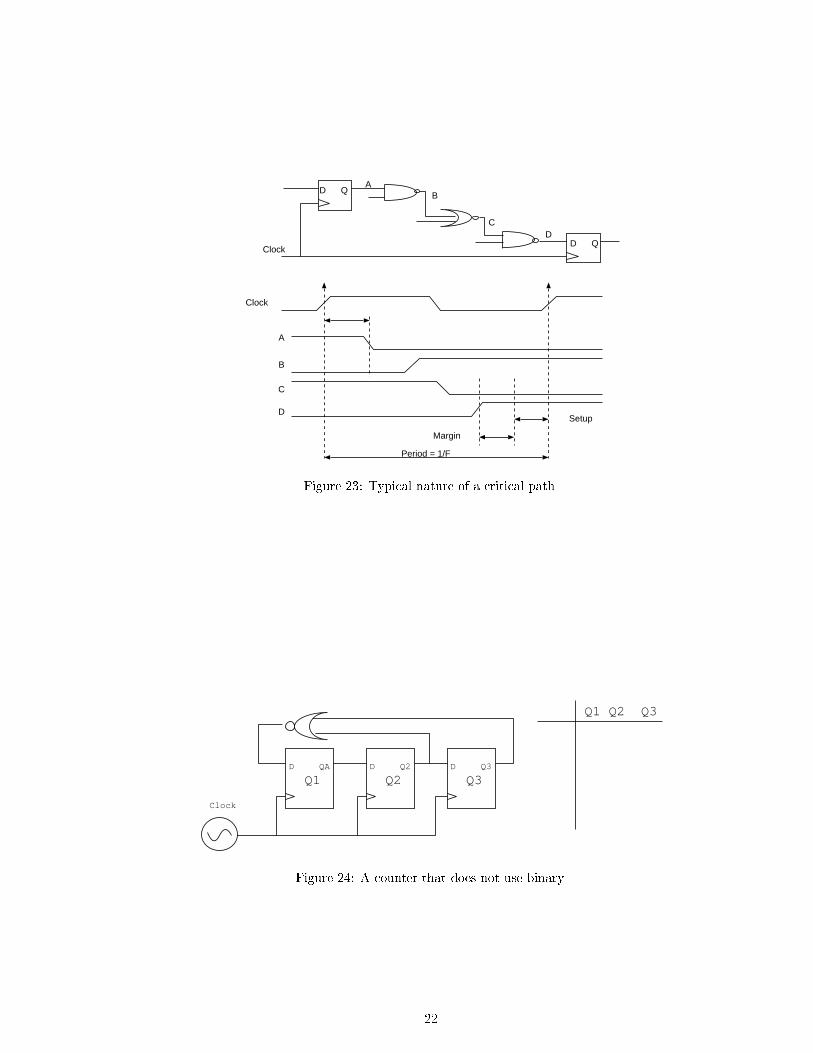
In a synchronous FSM, the maximum clock frequency is normally determined by the longest pathof logic which ends at the input of a ip- op. This path is know as the critical path and is illustratedin �gure 23.
2.2 Speed Increase with Johnson Counter
A Johnson counter is based around a shift register. Figure 24 shows a Johnson counter that dividesby �ve. The signi�cant features of Johnson counters actually become clearer for larger counters,but they are twofold: 1. the division ratio is restricted to twice the number of ip- ops (e.g. 5 ip- ops can give a divide by 10 at maximum) and 2. the number of logic gates is always low, andso the counter is fast.
Exercise: Design a Johnson Counter that also has a control input that makes it divide by six orseven. Optimise your design for two features: 1. maximum clock speed, 2. that the ratio input canbe changed at any time without causing a hazard. Note: clearly, metastability cannot be avoided,but by being hazard free, we mean that the state path taken will always be one or the other ofthe two desired paths, whatever happens. Why might the second feature be important in practice(hint: consider derived clocks) ?
2.3 Speed Increase with One Hot Coding
In One Hot coding, at all times, the ip- ops in a counter or FSM are arranged to be all zeroexcept for one that is one. This clearly minimises the number of gates required to decode thecurrent state and can greatly reduce the number of gates that determine the next state.
21
Clock
A
B
C
DSetup
Margin
Period = 1/F
Clock
D Q
D Q
AB
CD
Figure 23: Typical nature of a critical path.
D Q3D Q2D QA
Clock
Q1 Q2 Q3
Q1 Q2 Q3
Figure 24: A counter that does not use binary.
22

Data in
D Q
D Q
D Q
D Q
D Q
D Q
Synchronous global clock signal
Another input
Yet another input
An output
Yet another output
Another output still
Large loop-free combinatorial logic function
Data in
D Q
D Q
D Q
D Q
D Q
D Q
Synchronous global clock signal
Another input
Yet another input
An output
Yet another output
Another output still
Loop-free combinatorial logicfunction - second half
Desired logic function
Desired logic function - pipelined version.
D Q
D Q
D Q
D Q
Loop-free combinatorial logicfunction - first half
Figure 25: Example of introducing pipelining to increase throughput, but also delay.
2.4 Speed Increase using Pipelineing
Figure 25 shows a circuit before and after the addition of a pipelining stage. The pipeline stagemay have a fewer or greater number of ops as the input or output. The bene�t of the pipelinestage is that a complex combinatorial logic function is split into two halves, thereby reducing themaximum length of unclocked logic leading to the inputs of the output ip- ops. The disadvantageof the pipeline stage is that data takes longer to be processed. This disadvantage is not often aproblem: for instance, if the data has just come down a link in a network, then the additionaldelay will be just as if the link were a few meters longer. More than one stage of pipelining can beinserted if needed.
Some modern logic synthesiser tools will insert pipeline delays where possible, if helpful. Otherswill back-propagate them if they are instantiated at the outputs.
Exercise Sketch the circuit of a large adder with ripple carry and then modify it to include apipeline stage. Note, the output signals should always re ect the result of a single addition inany one clock cycle. Explain or estimate the e�ect of the pipeline delay on the maximum clockfrequency. If the adder is now used to form a counter where an input value N is added to anaccummulator register each clock cycle a) what goes wrong, and b) how can this be �xed ?
23

FSM
Mealy OutputsInputs
Moore Outputs
FSM
Mealy Outputs
Moore Outputs
FSM
Inputs
Clock
Moore
Mealy
Inputs
Figure 26: Cascading FSMs to produce larger circuits.
2.5 Derived Clocks.
Figure 26 shows a concatenation of �nite-state machines running from the same clock. Of course,canonicly, these together simply form one larger FSM. However, the decomposed view is vital inpractice, since the density of wiring between FSMs will be lower than within the FSM and thefunctionality, authorship, history and even ownership of the IPR (intellectual property rights) ofthe FSMs will be di�erent.
If we feed a Mealy output into another FSM, delays accumulate, reducing maximum clock fre-quency. This does not happen with Moore outputs. Moore outputs should be used if possible, butfor some designs, a Mealy output is needed in order to reduce processing delay of the unit as awhole.
24
Serialdata in
Serial clock
in
Paralleldata output
Word clockoutput
Divide by 5 counter
D D D D D
DDDDD
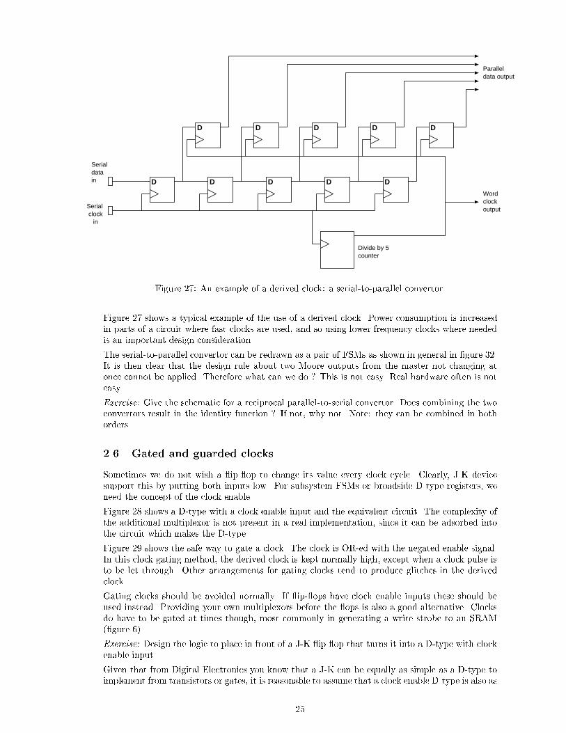
Figure 27: An example of a derived clock: a serial-to-parallel convertor.
Figure 27 shows a typical example of the use of a derived clock. Power consumption is increasedin parts of a circuit where fast clocks are used, and so using lower frequency clocks where neededis an important design consideration.
The serial-to-parallel convertor can be redrawn as a pair of FSMs as shown in general in �gure 32.It is then clear that the design rule about two Moore outputs from the master not changing atonce cannot be applied. Therefore what can we do ? This is not easy. Real hardware often is noteasy.
Exercise: Give the schematic for a reciprocal parallel-to-serial convertor. Does combining the twoconvertors result in the identity function ? If not, why not. Note: they can be combined in bothorders.
2.6 Gated and guarded clocks
Sometimes we do not wish a ip- op to change its value every clock cycle. Clearly, J-K devicesupport this by putting both inputs low. For subsystem FSMs or broadside D-type registers, weneed the concept of the clock enable.
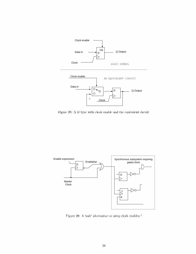
Figure 28 shows a D-type with a clock enable input and the equivalent circuit. The complexity ofthe additional multiplexor is not present in a real implementation, since it can be adsorbed intothe circuit which makes the D-type.
Figure 29 shows the safe way to gate a clock. The clock is OR-ed with the negated enable signal.In this clock gating method, the derived clock is kept normally high, except when a clock pulse isto be let through. Other arrangements for gating clocks tend to produce glitches in the derivedclock.
Gating clocks should be avoided normally. If ip- ops have clock enable inputs these should beused instead. Providing your own multiplexors before the ops is also a good alternative. Clocksdo have to be gated at times though, most commonly in generating a write strobe to an SRAM(�gure 6).
Exercise: Design the logic to place in front of a J-K ip op that turns it into a D-type with clockenable input.
Given that from Digital Electronics you know that a J-K can be equally as simple as a D-type toimplement from transistors or gates, it is reasonable to assume that a clock enable D-type is also as
25
D
Clock
Data in
Q Output
Clock enable
DData in Q Output
Clock enable
Clock
CE
LOGIC SYMBOL
AN EQUIVALENT CIRCUIT
1
0
Figure 28: A D-type with clock enable and the equivalent circuit.
D
Master Clock
D
Synchronous subsystem requiringgated clock
J
K
EnablebarEnable expression
Figure 29: A `safe' alternative to using clock enables ?
26

D Q
Delay
D Q
Delay
D Q
Delay
Data input Data outputQA QB
Clock
a) A three-stage shift register with some clock skew delays.
D Q
Delay
D Q
Delay
D Q
Delay
Data input Data outputQA QB
Clock
b) A three-stage shift register with data delays and clock skew delays.
Delay Delay
D Q
Delay
D Q
Delay
D Q
Delay
Data input Data outputQA QB
Clock
c) A solution for serious skew and delay problems ?
Delay Delay
Figure 30: Synchronous systems, but with clock skew.
simple. Therefore why should we ever use gated clocks instead of clock enable inputs ? The answeris that if we have a large number of ip- ops that are all to share the same clock-enable expression,we would have two penalties of using clock enable: 1. we have to route the clock enable signal toall of them, and 2. we have to make the ip- ops from logic which is capable of being clocked atevery opportunity. We use clock-enable inputs where single or smaller numbers of ip- ops are tobe enabled in unison, such as in a broadside register with clock enable. For single ip- ops, theclock enable is best considered as just one aspect of the FSM that the op is part of.
2.7 Clock and Data Skews
Skew is when a signal that is intended to arrive at several places at the same time actually arrivesat various times.
Figure 30 shows a shift register circuit with clock skew. Skew is the enemy of synchronous, �nite-state machines, since in the worst scenario, the output of one op may have changed, causing achange in the input to another op, before that second op has been clocked itself: this destroysthe FSM behaviour.
If there is considerable delay in both the data and the clock, and these delays are random, thenthe shift register is not likely to work well. An example of such a system is where the shift registeris actually a communications medium snaking around a number of circuit boards in a system. Thedelays are in the interconnecting cables. Typically, the logic at each station is not simply a D-type,but is logic which can read and change the data as it passes and the data may be a bus instead ofa single wire. In this case, the solution is to invert the clock at each hop.
Exercise: Draw a timing diagram for the inverting-the-clock solution and work out the maximumfrequency of operation. Use the following �gures: conductor delay random between 4 and 9nanoseconds, ip- op set-up time 2 nanoseconds, hold time 1 nanoseconds and propagation time 5nanoseconds. Note: in practice you would not run such a system close to the maximum you have
27
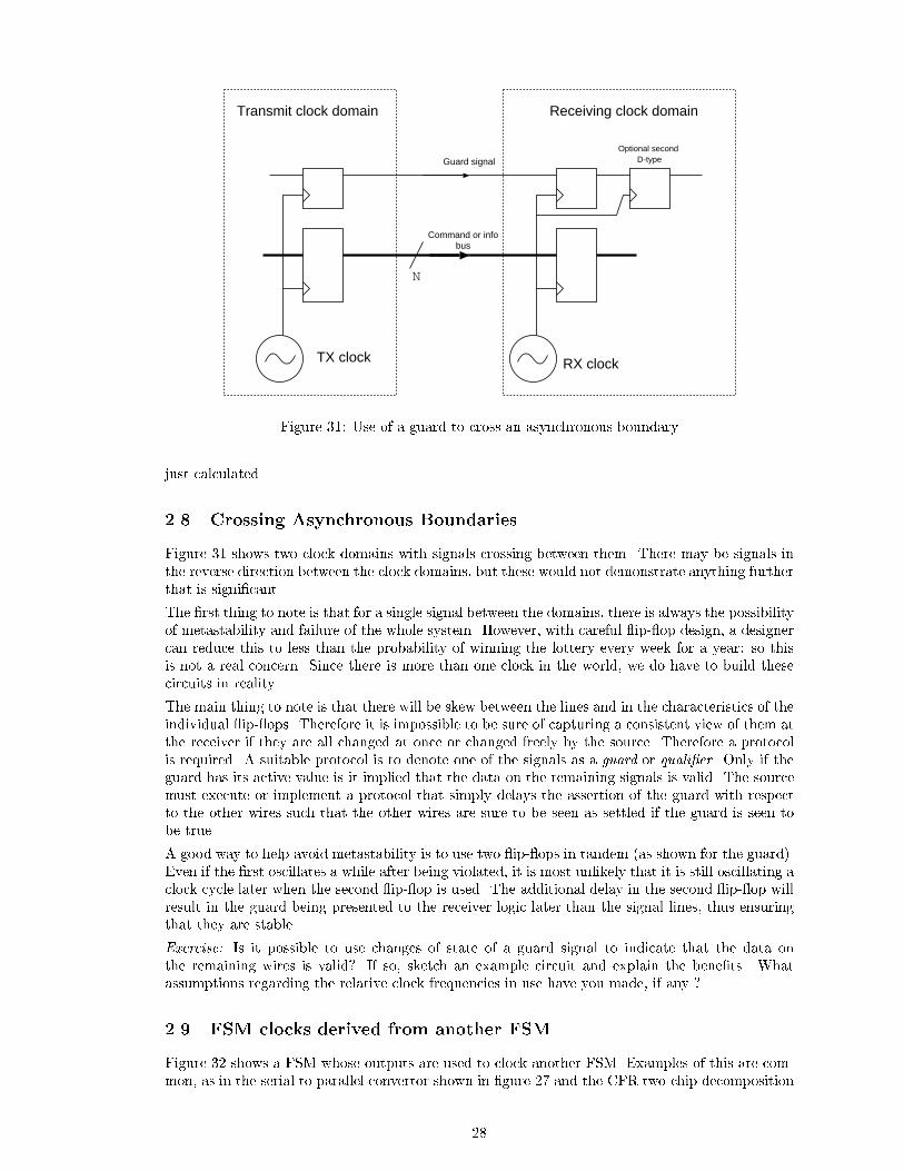
Receiving clock domainTransmit clock domain
TX clock RX clock
Guard signal
Command or infobus
N
Optional second D-type
Figure 31: Use of a guard to cross an asynchronous boundary
just calculated.
2.8 Crossing Asynchronous Boundaries
Figure 31 shows two clock domains with signals crossing between them. There may be signals inthe reverse direction between the clock domains, but these would not demonstrate anything furtherthat is signi�cant.
The �rst thing to note is that for a single signal between the domains, there is always the possibilityof metastability and failure of the whole system. However, with careful ip- op design, a designercan reduce this to less than the probability of winning the lottery every week for a year: so thisis not a real concern. Since there is more than one clock in the world, we do have to build thesecircuits in reality.
The main thing to note is that there will be skew between the lines and in the characteristics of theindividual ip- ops. Therefore it is impossible to be sure of capturing a consistent view of them atthe receiver if they are all changed at once or changed freely by the source. Therefore a protocolis required. A suitable protocol is to denote one of the signals as a guard or quali�er. Only if theguard has its active value is it implied that the data on the remaining signals is valid. The sourcemust execute or implement a protocol that simply delays the assertion of the guard with respectto the other wires such that the other wires are sure to be seen as settled if the guard is seen tobe true.
A good way to help avoid metastability is to use two ip- ops in tandem (as shown for the guard).Even if the �rst oscillates a while after being violated, it is most unlikely that it is still oscillating aclock cycle later when the second ip- op is used. The additional delay in the second ip- op willresult in the guard being presented to the receiver logic later than the signal lines, thus ensuringthat they are stable.
Exercise: Is it possible to use changes of state of a guard signal to indicate that the data onthe remaining wires is valid? If so, sketch an example circuit and explain the bene�ts. Whatassumptions regarding the relative clock frequencies in use have you made, if any ?
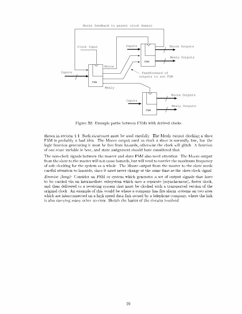
2.9 FSM clocks derived from another FSM
Figure 32 shows a FSM whose outputs are used to clock another FSM. Examples of this are com-mon, as in the serial to parallel convertor shown in �gure 27 and the CFR two-chip decomposition
28
FSM
Inputs
Clock Input
Moore
Mealy
FSM
Mealy Outputs
Moore Outputs
Inputs
FSM
Mealy Outputs
Moore OutputsInputs
Moore feedback to parent clock domain
Feedforward of outputs to son FSM
Figure 32: Example paths between FSMs with derived clocks
shown in section 4.4. Such structures must be used carefully. The Mealy output clocking a slaveFSM is probably a bad idea. The Moore output used to clock a slave is normally �ne, but thelogic function generating it must be free from hazards, otherwise the clock will glitch. A functionof one state variable is best, and state assignment should have considered that.
The non-clock signals between the master and slave FSM also need attention. The Moore outputfrom the slave to the master will not cause hazards, but will tend to restrict the maximum frequencyof safe clocking for the system as a whole. The Moore output from the master to the slave needscareful attention to hazards, since it must never change at the same time as the slave clock signal.
Exercise (long): Consider an FSM or system which generates a set of output signals that haveto be carried via an intermediate subsystem which uses a separate (asynchronous), faster clock,and then delivered to a receiving system that must be clocked with a transported version of theoriginal clock. An example of this would be where a company has �re alarm systems on two siteswhich are interconnected on a high speed data link owned by a telephone company, where the linkis also carrying many other services. Sketch the basics of the circuits involved.
29

Figure 33: A wafer outline showing where it will be diced (Chips are not always square).
DIE
PIN
PACKAGEBOND PADCAVITY
Figure 34: A chip in its package, ready for bond wires.
3 Technology
The cost of a system depends on the cost of its parts. There are many ways to design a systemand typically we want to minimise cost. Therefore, before you can design a system, you need to befamiliar with a vocabulary of technologies and pre-existing parts. You also need to know how toproduce new integrated circuits for your application design. Application-speci�c integrated circuits(ASICs) and make up a large fraction of the IC market by revenue.
3.1 Basics of ICs.
Note: this section is a briefest of introductions to VLSI.
Chips are made of Si or GaAs with layers of Al on top for signal wiring. Chips are made on arectangualr grid on a wafer of the substrate material. Wafers are about 0.3 mm thick and from 3to 8 inches in diameter. Most of the wafer depth is only present for handling reasons and the activeportion of the chip lies in the top few microns of the wafer or is built up above the top surface.
Wafers are processed using ion implantation and photo-resistive etching at elevated temperaturesin the presence of dopant and etchant gasses. Each photo-resist is �rst exposed to an ultravioletor X-ray source under a mask generated by the CAD tools. Between 7 and 25 masks might beused, depending on the technology. The masks are stepped over the wafer to form the rectangular
30

Connectionsto and fromcore logic
Pad powersupply
PadElectronics
SupplyPad
GroundRail
SignalBondPad
Edge of Die
Power Rail
GroundPad
CORE AREA
Figure 35: The corner of a typical chip showing IO and power pads.
array of chips. Masked areas are left with an intact layer of resist and then remain una�ected bythe next processing step, hence successive masks build up complex three dimensional structuresforming the active components and conductors. Typical chips are today made using 0.25 to 0.5micron feature sizes. The smaller a transistor the faster it operates.
A wafer contains many chips which are diced after wafer testing. The chip is then packaged toease handling and to dissipate heat.
A typical chip is 4 to 100 square millimetres.
Wires are connected to chips at bond pads. Bond pads are about 100 microns square and 150microns apart or half this size (linear dimension) in modern devices. The corner of a typical deviceis shown in Figure 35. Most chips have the shown power and ground `rings' around the outsidewith the bond pads in between. These rings provide low resistance power supplies to the pad logic.The pad logic is bu�er circuitry to provide high-power drive to o�-chip loads and to protect theinternal circuitry from external static discharges.
Figure 34 shows the chip carrier cavity containing a die. Connections are made from the conductorsin the package to the bond pads around the chip's perimeter using cold-welded gold wires.
3.2 Will an ASIC be core or pad bound ?
A chip may be either:
� Pad bound if it has many more pins than natural perimeter, or
� Core bound if it has su�cient active core area to dominate.
A pad bound chip is wasteful of area since we have to use a bigger die to get the pads on, but thebody of the die is not fully occupied with gates.
Generally we end up with separate fabrication processes for each of the following subsystems:
� memory,
31

� random logic,
� analogue circuits and analogue to/from digital conversion,
� high speed (e.g. clock rate greater than about 100 MHz).
Also, we must group together functions which can be implemented in the same technology, so theycan most easily be put on one chip. This is hard if the functions do not otherwise have much todo with each other: we might prefer to put the two sections of logic further apart.
3.3 Chip cost versus area
The cost of a chip divides into two parts: NRE and per-device cost.
NRE | non-recurring expenditure. NRE is paid once, regardless of how many devices are made.It consists of:
{ design cost (labour, computer time, management overheads),
{ mask making cost.
Per device | recurring expenditure consists of:
{ cost of basic silicon wafer,
{ cost of processing a wafer,
{ cost of testing devices,
{ cost of device packages and packaging,
{ cost of further testing, possibly under stressful conditions.
The per device cost is in uenced by the yield | the fraction of working dice.
The fraction of wafers where at least some of the die work is the `wafer yield' and is typically closeto 100 percent for a mature fabrication process.
The fraction of die which work on a wafer (often simply the `yield') depends on wafer impuritydensity and device size. Die yield goes down with chip area.
The fraction of devices which pass wafer probe (i.e. before the wafer is diced) and fail post packagingtests is very low. However, full testing of analog sections or other lengthy operations are typicallyskipped at the wafer probe stage.
3.4 Example of CMOS die cost
A six inch diameter wafer has area (3:14r2) = 18000 mm2:
A chip has area A, which can be anything between 2 to 200 mm2 (including scoring lines).
Dies per wafer is 18000=A
Processed wafer cost might be 5000 pounds. (Actually it's probably about one third this cost tothe silicon foundry, but there are overheads and pro�t to add on.)
Probability of working = wafer yield � die yield (assume wafer yield is 1.0 or else included in thewafer cost).
Assume 99.5 percent of square millimetres are defect free. Die yield is then
P (All A squares work) = 0:995A
cost of working dice is5000
18000
A0:995A
pounds each:
Here is a program to estimate the cost of a working die given a six inch wafer with a processingcost of 5000 pounds and a probability of a square millimetre being defect free of 99.55 percent. Itsoutput is shown in table 1.
32

Area Wafer dies Working dies Cost per working die
2 9000 8910 0.56
3 6000 5910 0.85
4 4500 4411 1.13
6 3000 2911 1.72
9 2000 1912 2.62
13 1385 1297 3.85
19 947 861 5.81
28 643 559 8.95
42 429 347 14.40
63 286 208 24.00
94 191 120 41.83
141 128 63 79.41
211 85 30 168.78
316 57 12 427.85
474 38 4 1416.89
Table 1: Output from the die cost program.
#include <math.h>
display(double area)
{
double dies = 18000.0 / area;
double yield = dies * pow(0.995, area);
double cost = 5000.0 / yield;
printf("%.0f %.0f %.0f %.2f\n", area, dies, yield, cost);
}
int main()
{
double area = 2.0; /* area in square mm */
while (area < 500.0)
{
display(area);
area = trunc(area * 1.5);
}
}
Large dies sometimes use redundant design such that one, two or three faults can be tolerated.Laser or ion beam trimming is used to patch out faulty sections (of say a RAM array) and substitutepreviously redundant sections.
Exercise: Given that the cost of patching a die doubles its processing cost and is 90 percentsuccessful and requires 10 percent additional area in the design, for what size and type of deviceis it suitable ? It is necessary to make various assumptions to answer this.
3.5 Classes of Integrated Circuits
Figure 36 presents a taxonomy of chip design approaches. The top-level division is between stan-dard parts, ASICs and �eld programmable parts.
3.5.1 Standard Parts
A standard part is essentially any chip that a chip manufacturer is prepared to sell to someoneelse along with a datasheet. The design may actually previously have been an ASIC for a speci�ccustomer which is now on general release. However, most standard parts are general purpose logic,memory and microprocessor devices. These are normally full custom designs designed in-house bythe chip manufacturer to make the most of in-house fabrication line, perhaps using optimisationsnot made available to others who use the line as a foundry. Other standard parts include graphicscontrollers, LAN controllers, bus interface devices, and miscellaneous useful chips.
33

StandardParts
SemiCustom
FullCustom
StandardCell
GateArray
Integrated Circuits
MaskedASICs
FieldProgrammable
Parts
FPGAArrayLogic(PALs)
CommodityParts
General Chip Products
Figure 36: A taxonomy of integrated circuits.
3.5.2 Masked ASICs.
A masked ASIC (application speci�c integrated circuit) is a device manufactured for a customerinvolving a set of masks where at least some of the masks are used only for that device. Thesedevices include full-custom and semi-custom ASICs.
A full-custom chip (or part of a chip) has had detailed manual design e�ort expended on its circuitsand the position of each transistor and section of interconnect. This allows an optimum of speedand density and power consumption.
Full-custom design is used for devices which will be produced in very large quantities: e.g. millionsof parts where the design cost is justi�ed. Full-custom design is also used when required forperformance reasons. Microprocessors, memories and digital signal processing devices are primaryusers of full-custom design.
In semi-custom design, each cell has a �xed design and is repeated each time it is used, both withina chip and across many devices which have used the library. This simpli�es design, but drive powerof the cell is not optimised for each instance.
Semi-custom is achieved using a library of logic cells. Figure 45 shows a cell from the data bookfor a standard cell library. This device has twice the `normal' drive power, which indicates one ofthe compromises implicit in standard cell over full-custom, which is that the size (driving power)of transistors used in a cell is not tuned on a per-instance basis.
There are two types of semi-custom devices:
� standard cell
� gate array.
In standard cell designs, cells from the library can freely be placed anywhere on the device andthe number of IO pads and the size of the die can be freely chosen. Clearly this requires that allof the masks used for a device are unique to that device and cannot be used again. (Mask makingis one of the largest costs in chip design).
In gate array designs, the silicon vendor o�ers a range of chip sizes. Each size of chip has a �xedlayout and the location of each transistor, resistor and IO pad is common to every design that usesthat size. A gate array is con�gured for a particular design by wiring up the transistors (and other
34

components) in the desired way. Many transistors will be unused. The wiring up is, as usual, donewith the top two or three layers of metal wiring. Therefore only two or three masks need be madeto make a new design.
Silicon vendors will typically have stocks of wafers which have had the bottom 15 to 20 processsteps made and are only awaiting �nal metalisation to be turned into usable devices. Hence designtime is low. Risk is also low since the �nished chip has only a small NRE cost and gate arraytechnology is intrinsically conservative and hence reliable.
The disadvantage of gate arrays is their intrinsic low density of active silicon.
Standard cell designs use a set of well-proven logic cells on the chip, much in the way that previousgenerations of standard logic have been used as board-level products, such as Texas Instruments'System 74.
A variation on the semi-custom approach is to include full-custom macrocells such as processorcores in �xed positions on the wafer.
Exercise: Ignoring the title, determine from the data sheet whether the cell in �gure 45 is forstandard cell or gate array use ? What other information about the cell is needed to prepare anaudit of resources used in a design which has used this cell ? The audit refered to is typically areport generated by the CAD tools which gives summary information.
3.5.3 Field programmable logic
About 25 to 40 percent of chip sale revenue now comes from �eld programmable logic devices.These are chips which can be programmed electronicly on the user's site to provide the desiredfunction. The Xilinx FPGA parts used in the Part 1B E+A classes are one of the most importantexamples of �eld programmable logic.
Field programmable devices may be volatile (need programming every time after power up), repro-grammable or one-time programable. This relates to how the programming information is storedinside the devices, which can be in RAM cells or in any of the ways mentioned for ROM devicesin section 1.2.
3.5.4 FPGAs
An FPGA (�eld programmable gate array) consists of an array of con�gurable logic blocks (CLBs),as shown in Figure 37. Not shown is that the device also contains a good deal of hidden logic usedjust for programming it. Some pins are also dedicated to programming. Such FPGA devices havebeen popular since about 1990.
Each CLB (Figure 38) typically contains one or two ip- ops, and has a few (�ve shown) gen-eral purpose inputs, some special purpose inputs (only a clock is shown) and two outputs. Theillustrated CLB is of the look-up table type, where the logic inputs index a small section of pre-con�gured RAM memory which implements the desired logic function. For �ve inputs and oneoutput, a 32 by 1 SRAM is needed. Some FPGA families now give the designer write access tothis SRAM, thereby greatly increasing the amount of storage available to the designer. However,it is still an expensive way to buy memory.
All CLBs within a FPGA generally have the same structure, but FPGAs are available with lowerand higher functionality CLBs. The best size of CLB is not yet clear. Modern designs of FPGAhave a heirarchy of CLB internconnection patterns, giving CLB clusters within clusters.
An FPGA is very like a mask-programmed gate array to use. The design ow and CAD tools arevirtually identical. The expenditure before the designer has the �rst device in her hands might be1000 times lower. The cost of further devices is at least 10 times higher than mask-programmeddevices, owing to the programming cost and wasted die area devoted to the programming activities.Clearly there is a crossover production volume point!
FPGAs also tend to be quite slow, owing to the signals passing through hidden logic used only forcon�guration.
35

CLB
SWITCHMATRIX
CLB
SWITCHMATRIX
CLB
SWITCHMATRIX
CLB
SWITCHMATRIX
CLB
SWITCHMATRIX
CLB
SWITCHMATRIX
CLB
SWITCHMATRIX
CLB
SWITCHMATRIX
CLBCLB CLB
CLB
SWITCHMATRIX
CLB
CLB
SWITCHMATRIX
SWITCHMATRIX
Bondpad
IOB
Bondpad
IOB
Bondpad
IOB
Bondpad
Bondpad
IOBBondpad
IOBBondpad
IOB
Edge of die
Figure 37: Field programmable gate array structure, showing IO blocks around the edge, inter-connection matrix blocks and con�gurable logic blocks.
Generalinputs
Combinatorialfunctiongenerator
D Q
D Q
Clock input
First output
Second Output
Programmable multiplexers
Figure 38: A con�gurable logic block for a look-up-table based FPGA.
36
Bond PAD
Input buffer
Input
Output
Tristatecontrol
Outputenable
Programmablemultiplexor
1
0
Output buffer
Connectionsto
centralarray.
Figure 39: A simple IO block for an FPGA.
Often a designer or company will build prototypes and early production units using FPGAs andthen use a drop-in mask-programmed equivalent once the design is mature and sales volumes pickup.
Exercise: Attempt to sketch the logic needed inside one of the programmable switch matrix boxes.You should �nd this is a vast amount of logic and therefore understand why FPGAs are so expensivefor their functionality. (If you know how to use pass transistors, this will help your design).
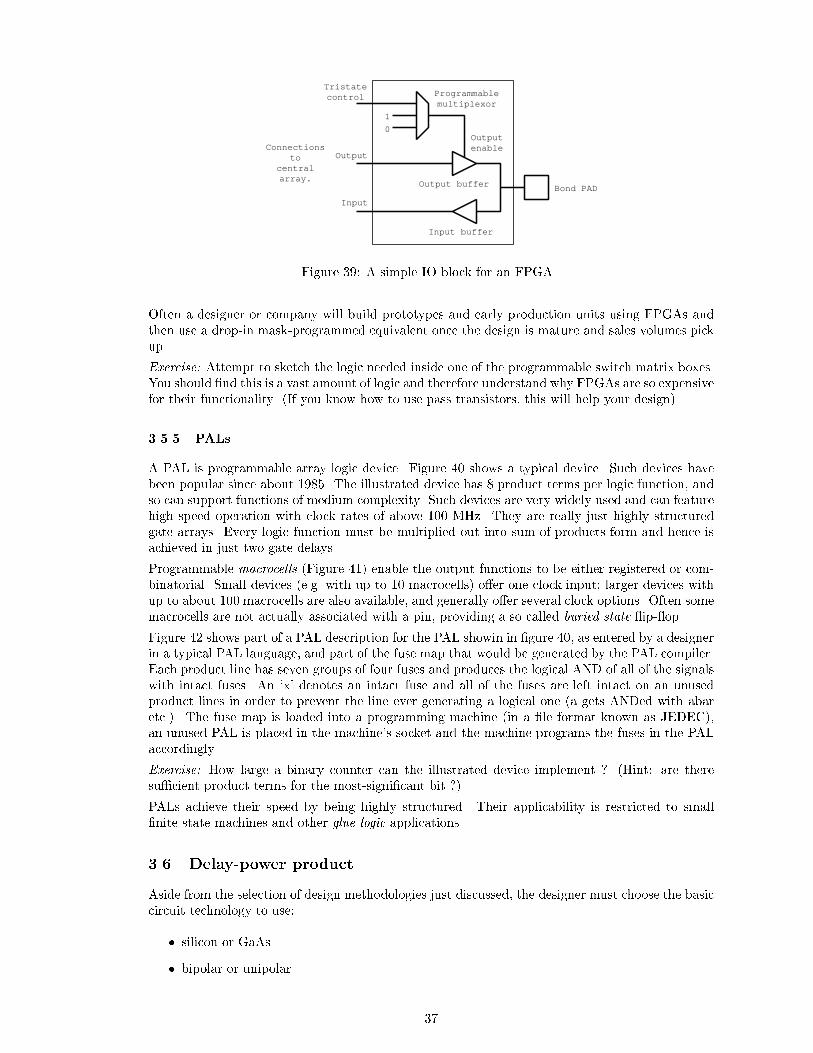
3.5.5 PALs
A PAL is programmable array logic device. Figure 40 shows a typical device. Such devices havebeen popular since about 1985. The illustrated device has 8 product terms per logic function, andso can support functions of medium complexity. Such devices are very widely used and can featurehigh speed operation with clock rates of above 100 MHz. They are really just highly structuredgate arrays. Every logic function must be multiplied out into sum-of-products form and hence isachieved in just two gate delays.
Programmable macrocells (Figure 41) enable the output functions to be either registered or com-binatorial. Small devices (e.g. with up to 10 macrocells) o�er one clock input; larger devices withup to about 100 macrocells are also available, and generally o�er several clock options. Often somemacrocells are not actually associated with a pin, providing a so called buried state ip- op.
Figure 42 shows part of a PAL description for the PAL showin in �gure 40, as entered by a designerin a typical PAL language, and part of the fuse map that would be generated by the PAL compiler.Each product line has seven groups of four fuses and produces the logical AND of all of the signalswith intact fuses. An `x' denotes an intact fuse and all of the fuses are left intact on an unusedproduct lines in order to prevent the line ever generating a logical one (a gets ANDed with abaretc.). The fuse map is loaded into a programming machine (in a �le format known as JEDEC),an unused PAL is placed in the machine's socket and the machine programs the fuses in the PALaccordingly.
Exercise: How large a binary counter can the illustrated device implement ? (Hint: are theresu�cient product terms for the most-signi�cant bit ?)
PALs achieve their speed by being highly structured. Their applicability is restricted to small�nite state machines and other glue logic applications.
3.6 Delay-power product
Aside from the selection of design methodologies just discussed, the designer must choose the basiccircuit technology to use:
� silicon or GaAs
� bipolar or unipolar
37

Powersupplypin
Clocksignal
Clockinput
Generalpurposeinputs
Productline
Termline
Outputpad
(can alsobe input).
Outputenable
product line
Groundpin.
The crosspoints in
these shadedregions
areprogrammable
points
Macro-cell
Macro-cell
Macro-cell
1
2
3
4
5
6
7
8
910
11
12
13
14
15
16
17
Figure 40: A typical PAL with 7 inputs and 7 I/Os.
38

Inputbuffer
Clock Net
I/O Pad
Tristateoutput pad
Programmablemultiplexor
D-typeflip-flop
D QMain input
S-of-P
Output enableterm
Feedback toarray
Figure 41: Contents of the PAL macrocell.
pin 16 = o1;
pin 2 = a;
pin 3 = b;
pin 4 = c
o1.oe = ~a;
o1 = (b & o1) | c;
-x-- ---- ---- ---- ---- ---- ---- (oe term)
--x- x--- ---- ---- ---- ---- ---- (pin 3 and 16)
---- ---- x--- ---- ---- ---- ---- (pin 4)
xxxx xxxx xxxx xxxx xxxx xxxx xxxx
xxxx xxxx xxxx xxxx xxxx xxxx xxxx
xxxx xxxx xxxx xxxx xxxx xxxx xxxx
xxxx xxxx xxxx xxxx xxxx xxxx xxxx
xxxx xxxx xxxx xxxx xxxx xxxx xxxx
x (macrocell fuse)
Figure 42: Example programming of a PAL showing only fuses for the top macrocell.
39
Delay (ns)
Power pergate (mW).
0.1 1.0 10 100 1000
1
10
100 ECL
TTL
CMOS
Lines of constantdelay-power product
1980
1990
2000
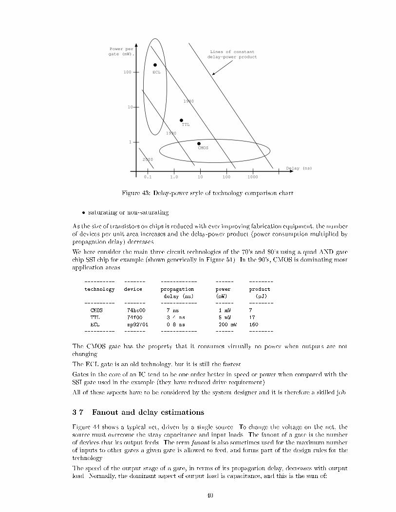
Figure 43: Delay-power style of technology comparison chart.
� saturating or non-saturating.
As the size of transistors on chips is reduced with ever improving fabrication equipment, the numberof devices per unit area increases and the delay-power product (power consumption multiplied bypropagation delay) decreases.
We here consider the main three circuit technologies of the 70's and 80's using a quad AND gatechip SSI chip for example (shown generically in Figure 51). In the 90's, CMOS is dominating mostapplication areas.
---------- ------- ------------ ------ --------
technology device propagation power product
delay (ns) (mW) (pJ)
---------- ------- ------------ ------ --------
CMOS 74hc00 7 ns 1 mW 7
TTL 74f00 3.4 ns 5 mW 17
ECL sp92701 0.8 ns 200 mW 160
---------- ------- ------------ ------ --------
The CMOS gate has the property that it consumes virtually no power when outputs are notchanging.
The ECL gate is an old technology, but it is still the fastest.
Gates in the core of an IC tend to be one order better in speed or power when compared with theSSI gate used in the example (they have reduced drive requirement).
All of these aspects have to be considered by the system designer and it is therefore a skilled job.
3.7 Fanout and delay estimations.
Figure 44 shows a typical net, driven by a single source. To change the voltage on the net, thesource must overcome the stray capacitance and input loads. The fanout of a gate is the numberof devices that its output feeds. The term fanout is also sometimes used for the maximum numberof inputs to other gates a given gate is allowed to feed, and forms part of the design rules for thetechnology.
The speed of the output stage of a gate, in terms of its propagation delay, decreases with outputload. Normally, the dominant aspect of output load is capacitance, and this is the sum of:
40

Parasitic
input
capacitance
Track to substrate
capacitance proportional
to total track length (area)
Driving
Gate
Driven
gates
Figure
44:Logicnet
with
trackingandinputloadcapacita
nces.
Simulator/HDL Call
NAND4 Standard Cell
4 input NAND gate with x2 drive
Schematic Symbol
NAND4X2(f, a, b, c, d);
ELECTRICAL SPECIFICATIONSwitching characteristics : Nominal delays (25 deg C, 5 Volt, signal rise and fall 0.5 ns)
Inputs Outputs
O/P Falling O/P Rising
ABCD
FFFF
(ps) ps/LU ps ps/LU
142161165170
37373737
198249293326
33333334
Min and Max delays depend upon temperature range, supply voltage, input edge speed and processspreads. The timing information is for guidance only. Accurate delays are used by the UDC.
: (One load unit = 49 fF)
Parameters
Input loading
Drive capability
Pin
abcd
f
Value
2.12.12.12.0
35
Load units
Load units
Units
a
b
c
d
f
Logical Function
F = NOT(a & b & c & d)
Library: CBG0.5um
X2
CELL PARAMETERS
Figure
45:Anexamplecell
from
amanufactu
rer'scell
library.
41

1. the capacitance proportional to the area of the output conductor
2. the sum of the input capacitances of the devices fed.
To estimate the delay from the input to a gate, through the internal electronics of a gate, throughits output structure and down the conductor to the input of the next gate, we must add threethings:
1. the internal delay of the gate, termed the intrinsic delay
2. the reduction in speed of the output stage, owing to the fanout/loading, termed the deratingdelay,
3. the propagation delay down the conductor.
The propagation delay down a conductor obeys standard transmission line formula and dependson the distributed capacitance, inductance and resistance of the conductor material and adjacentinsulators. For circuit board traces, resistance can be neglected and the delay is just the speed oflight in the circuit board material: about 7 inches per nanosecond, or 200 metres per microsecond.
On a chip, the speed of light can be neglected because chips are physically small, but the resistanceof the aluminum conductors is su�ciently large to have an e�ect for critical applications, such asmaster clock signals.1
The upshot of this is that on a chip, we can mostly neglect the third aspect of delay, whereas on acircuit board, we need to model certain critical conductors as components in themseleves. Thesehave a simple delay model, whose value can be set by post routing back annotation.
The �rst two aspects of delay may easily be absorbed into the model for a component. We can usethe following formula
device delay = (intrinsic delay) + (output load � derating factor).
The intrinsic speed of a device is given in its data sheet, as is the derating factor and the loadingfactor of its inputs. Typical values for a standard cell array are shown in Figure 45. The outputload is the sum of a track dependent part and the fanout dependent part.
The track dependent part is a library constant times the track area.
The load dependent part is the sum of the input loads of all of the devices being fed.
Exercise: How true is the above model of signal delay when we use �eld programmable gatearrays with high e�ective track resistance ? The conductors on FPGAs consist of many sectionsof real metalic conductor interconnected by the user-programmed connection points. We thenhave considerable resistances at points along each conductor's path. How would you estimate thevarious delays for the staggered arrival of a signal on each part of the net ?
3.8 Comparative view of digital logic technologies
Table 2 gives some randomish numbers for what can be achieved with today's chips. These numbersare only accurate to about half an order of magnitude. Technology is always advancing!
For CMOS technology, the number of transistors on a chip and the clock rate both seem to doubleevery three years.
1Older technologies used polysilicon interconnections which had signi�cant resistance and so the di�erent gates
connected to a polysilicon net would experience di�erent arrival times of a signal at their inputs.
42

Maximum Maximum Maximum
Technology clock speed gate count pin count
GaAs bipolar 50 GHz 50 5
GaAs fet 3 GHz 300 100
Si ECL 3 GHz 5000 300
Si CMOS 400 MHz 1 E6 500
Within Si CMOS
Full-custom 400 MHz 1 E6 500
Standard cell 200 MHz 40000 500
Gate array 100 MHz 20000 500
PAL 75 MHz 500 68
FPGA 35 MHz 4000 200
Table 2: Approximate limits on contemporary technology.
4 Hardware, Software and Design Partition.
A hardware system can be designed using only hardware or hardware with an embedded processorand software in ROM. Perhaps several processors are to be used. A design also must be partitionedinto standard components and application speci�c integrated circuits (ASICs). The choice of whichparts of the design are realised in what technology is the design partition problem.
4.1 Embedded Systems
A processor which is permanently connected to a single ROM which contains all of the softwarethat the processor will ever execute is called an embedded processor. Here we consider when to usean embedded processor, and then, when using one, the designer has to chose whether to design anew one or use an existing one.
The main di�erence between a hardware solution and a software solution is the degree of paral-lelism. Processors typically execute one instruction at a time, reusing the same hardware com-ponents again and again. Hardware solutions typically have dedicated circuits for each function.If most of the hardware is likely to be idle for most of the time, a processor is prefered, but if aprocessor cannot achieve the throughput required, increased parallelism using hardware is prefered.
Complex functions normally require a processor, but CAD tools are evolving, allowing complexfunctions to be expressed alogrithmicly but implemented in logic gates.
High speed processing normally requires dedicated hardware. For instance, consider the errorcorrection performed by a CD player to overcome dirt and scratches. When CD players �rst cameout, this error correction was done with dedicated hardware, but today, microprocessors haveincreased in speed, and so the function can be done using the processor which is already thereto provide other complex functions (e.g. track skip). However, on the latest, 24 speed CD ROMdrives for computers, the error correction must be done 24 times faster, and so dedicated hardwareis re-introduced.
Processors give exibility: if the design is likely to be changed in minor ways to form new models,or to provide �eld upgrades, then using a processor and providing a new software release is a goodtechnique.
Standard processor chips can be very cheap for a given performance. This is because a very greatdeal of e�ort is put into their design and they are sold in large quantites, thereby reducing price.Part of the cost of any product is in testing it. A standard processor not only comes with its owntest quali�cation programme, it is able to execute software to help test the rest of the system.
Processors can be placed on an ASIC.
The decision to design and use a custom processor for an application should not be taken lightly.It can be useful, however, when the application is very simple or highly specialised. Examplesare signal processing, where a particular algortihm needs to be executed at high speed to track amissile or assist computer vision.
43

D QD Q D Q D Q
D Q
D Q
D QD Q D Q D QD Q
First operand
Second operand
Serial sum
Carry
Full adder
+
Figure 46: Addition of two integers serially, l.s.b. �rst
4.2 Logic Synthesis and Collapsing
If one considers an embedded processor connected to a ROM, it may be viewed as one large FSM.Since for any given piece of software, the ROM is unlikely to be full and there are likely to beresources in the processor that are not used by that software, the application of a good qualitylogic minimiser to the system, while it is in the design database, could trim it greatly. In most realdesigns, this will not be helpful: for instance, the advantages of full-custom applied to the processorcore will be lost. Infact, the minimisation function may be too complex for most algorithms totackle on today's computers.
However, there are cases that are practical. For instance, many digitial signal processing applica-tions do use this approach. A processing algorithm typically consists of multiple stages with namessuch as pre-emphasis, equalisation, coe�cient adaptation, �t, deconvolution and reconstruction.Each of these steps normally has to be done as fast as possible and so parallelism through multipleinstances of ALU and register hardware is needed. However, there can be data dependencies inthat one step cannot be done until the previous is completed, or in that two steps take the sameamount of processing as one other step. In these cases, we desire to reuse the same hardware foreach step. The Cathederal DSP compiler is the most famous tool for helping design such circuits.It performs folding of the algorithm to reuse hardware from one step in the next.
Bit-serial arithmetic is also a key approach in custom signal processing. The adder shown in�gure 46 requires only about 10 gates to add any number of bits. It operartes l.s.b. �rst so thatthe carry from one digit is available for the next digit. The clock speed for the calculation doesnot need to be reduced if longer words must be consumed, but the pipeline delay does go up.Multiplication is also easy in bit serial form, as shown for multiplication by a constant in �gure 47.Consider the same functions implemented in naive, broadside implementations.
A battery operated walkman CD ROM player may implement a great deal of DSP. The printing onthe unit may advertise `8 times oversampling D-to-A bitstream convertor and MASH bit mapping'.The processing power required for this is as much an Intel Pentium can produce, but through theuse of bit serial arithmetic, it takes very little power or silicon area.
The problem with bit-serial processing for the human designer is that it is very tricky to work outwhere individual bits are at any one time, and the optimisations that are possible cannot readilybe seen by the human. Therefore, good quality CAD tools are vital in the design of such systems.
4.3 ASICs
The cost of developing an ASIC has to be compared with the cost of using an existing part. Theexisting part may not perform the required function exactly, requiring either a design speci�cationchange, if possible, and/or some additional glue logic to adapt the part to the application.
More than one ASIC may be needed under any of the following conditions:
44

D Q
D QD Q D Q D QD Q
Input operand
Serial product
Carry
Full adder
+
Figure 47: Bit-serial multiplication of an integer by a hardwired constant
� application speci�c functions are physically distant
� application speci�c functions require di�erent technologies
� application speci�c functions are just too big for one ASIC
� it is desired to split the cost and risk or reuse part of the system later on.
Factors to consider on a per chip basis:
� pad count limitation (pad density limit of 15 per mm)
� power consmption limitation (powers above 5 Watts need special attention)
� gate count limitation (above 100 kgates is big for CMOS)
� speed of operation | in uences choice of technology
� will it be core or pad bound ?
� special considerations :
{ special static or dynamic RAM needs
{ mixed with analogue parts ?
{ high power handling outputs for load control: e.g. motors.
� availability of a developed module for future reuse
Power dissipation is generally proportional to:
Power / (clock speed) � (number of gates) � (supply voltage squared).
Various technologies can be positioned in the speed-power plane, as shown in Figure 43 and astime goes by, things get better.
4.4 Partitioning example: The Cambridge Fast Ring two chip set.
Two devices were developed for the CFR local-area network, illustrating the almost classical designpartition required in high-speed networking. They were never given grander names than the ECLchip and the CMOS chip. The block diagram for an adaptor card is shown in Figure 48.
The ECL chip clocks at 100 MHz and contains the minimal amount of logic that needs to clock atthe full network clock rate. Its functions are:
� implement serial transmission modulator and demodulator
45

8
8
8
DRAM
CMOSCHIP
(StandardPart)
ECLCHIP
Isolatingtransformers
RingConnector
VCO(analogue)
InterruptPAL
Standard databuffers
Address PAL
HostBus
12.5 MHz
100 MHz
Figure 48: Example of a design partition | the adaptor card for the Cambridge Fast Ring.
� convert from 1 bit wide to 8 bits wide and the other way around
� perform reception byte alignment (when instructed by logic in the CMOS chip).
Other features:
� ECL logic can support analogue line receivers at low additional cost so can receive theincoming signal directly on to the chip.
� ECL logic has high output power if required (1 volt into 25 ohms) and so can drive outgoingtwisted pair lines directly.
The CMOS chip clocks at one-eigth the rate and handles the complex logic functions:
� CRC generation
� full/empty bit protocol
� minipacket storage in on-chip RAM
� host processor interface
� ring monitoring and maintenance functions.
The ECL chip has at least 50 times the power consumption of the CMOS chip. The CMOS chiphas more than 50 times the gates of the ECL chip.
Two standard parts are used to augment the CFR set: the DRAM chip incorporates a densememory array which could not have been achieved for anywhere near the same cost onboard theCMOS chip and the VCO (Voltage Controlled Oscillator) device used for clock recovery was lefto� the ECL chip since it was a di�cult-to-design analogue component where the risk of having iton the chip was not desired.
PALs are used to `glue' the network interface itself to a particular host system bus. Only the gluelogic needs to be redesigned when a new machine is to be �tted with the chipset. PALs have ashort design turn-around time since they are �eld programmable.
46

Telephoneline interface
Off-hook relay
Isolationtransformer
A-to-D
D-to-A
MainDSP
processor
Single-chipprocessor
RS-232line drivers
Computerinterface
Led indicators
Power supplyconditioning
Ringdetector
DSPROM
DSPRAM
Directionalisolator
NV-RAM
DC powerinput
Figure 49: Example of a design partition | an external modem.
4.5 Partitioning example: An external PC Modem.
Figure 49 shows the block diagram of a typical modem. The illustrated device is an externalmodem, meaning that it sits in a box beside the computer and has an RS-232 serial connection tothe computer. It also requires its own power supply.
The device contains a few analog components which behave broadly like a standard telephone,but most of it is digital. A relay is used to connect the device to the line and its contacts mirrorthe `o�-hook' switch which is part of every telephone. It connects a transformer across the line.The relay and transformer provide isolation of the computer ground signal from the line voltages.Similarly the ringing detector often uses a optocoupler to provide isolation. Clearly, these analogaspects of the design are particular to a modem and are designed by a telephone expert.
Modems from the 1960's implemented everything in analog circuitry since microprocessors werenot then possible. Today, two microprocessors are often used, but as processing power increases,this can be reduced to one (or sometimes even none, if the main processor of a PC provides thefunctions needed).
The reason for two processors are interesting and will be discussed in lectures.
Note that the non-volatile RAM requires a special manufacturing processing step and so in notincluded as a resource on board the singe chip processor. Similarly, the RS-232 drivers need tohandle voltages of +/- 12 volts and so these cannot be included on chip without increasing thecost of the rest of the chip by using a fabrication proceess which can handle these voltages. TheNV-RAM is used to store the owner's settings, such as whether to answer an incoming call andwhat baud rate to attempt a �rst connection, etc..
47
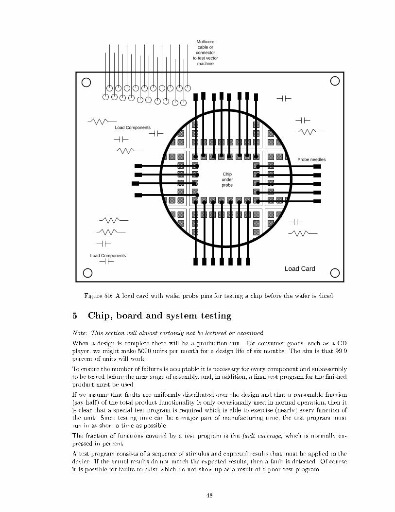
Chipunderprobe
Probe needles
Load Card
Load Components
Load Components
Multicorecable or
connectorto test vector
machine
Figure 50: A load card with wafer probe pins for testing a chip before the wafer is diced.
5 Chip, board and system testing.
Note: This section will almost certainly not be lectured or examined.
When a design is complete there will be a production run. For consumer goods, such as a CDplayer, we might make 5000 units per month for a design life of six months. The aim is that 99.9percent of units will work.
To ensure the number of failures is acceptable it is necessary for every component and subassemblyto be tested before the next stage of assembly, and, in addition, a �nal test program for the �nishedproduct must be used.
If we assume that faults are uniformly distributed over the design and that a reasonable fraction(say half) of the total product functionality is only occasionally used in normal operation, then itis clear that a special test program is required which is able to exercise (nearly) every function ofthe unit. Since testing time can be a major part of manufacturing time, the test program mustrun in as short a time as possible.
The fraction of functions covered by a test program is the fault coverage, which is normally ex-pressed in percent.
A test program consists of a sequence of stimulus and expected results that must be applied to thedevice. If the actual results do not match the expected results, then a fault is detected. Of courseit is possible for faults to exist which do not show up as a result of a poor test program.
48
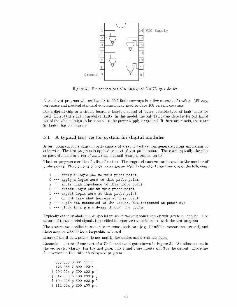
1
2
3
4
5
6
7 8
9
10
11
12
13
14 VCC Supply
Ground
Figure 51: Pin connections of a 7400 quad NAND gate device.
A good test program will achieve 98 to 99.5 fault coverage in a few seconds of testing. Military,aerospace and medical standard equipment may need to have 100 percent coverage.
For a digital chip or a circuit board, a tangible subset of `every possible type of fault' must beused. This is the stuck at model of faults. In this model, the only fault considered is for one singlenet of the whole design to be shorted to the power supply or ground. If there are n nets, there are2n faults that could occur.
5.1 A typical test vector system for digital modules
A test program for a chip or card consists of a set of test vectors generated from simulation orotherwise. The test program is applied to a set of test probe points. These are typically the pinsor pads of a chip or a bed of nails that a circuit board is pushed on to.
The test program consists of a list of vectors. The length of each vector is equal to the number ofprobe points. The elements of each vector are an ASCII character taken from one of the following:
1 --- apply a logic one to this probe point
0 --- apply a logic zero to this probe point
z --- apply high impedance to this probe point
H --- expect logic one at this probe point
L --- expect logic zero at this probe point
x --- do not care what happens at this point
p --- a pin not connected to the tester, but connected to power etc.
c --- clock this pin mid-way through the cycle.
Typically other symbols enable special pulses or varying power supply voltages to be applied. Thenature of these special signals is speci�ed in separate tables included with the test program.
The vectors are applied in sequence at some clock rate (e.g. 10 million vectors per second) andthere may be 100000 for a large chip or board.
If any of the H or L points do not match, the device under test has failed.
Example | a test of one part of a 7400 quad nand gate shown in Figure 51. We allow spaces inthe vectors for clarity. For the �rst gate, pins 1 and 2 are inputs and 3 is the output. There arefour vectors in this rather inadequate program.
000 000 0 001 111 1
123 456 7 890 123 4
[ 00H 00x p H00 x00 p ]
[ 01x 00H p H00 x00 p ]
[ 10x 00H p H00 x00 p ]
[ 11L 00x p H00 x00 p ]
49

Exercise: Write a 100 percent coverage test program for a 7400.
5.2 The need for test modes.
For some designs it would take a very long test program to test certain functions. For example, theleap year circuitry in a digital watch is might need four years' worth of clock pulses before beingexercised. Therefore, the throughput of the testing station would be low.
For other designs, the observability of internal state can be low. This occurs when there is a lotof internal state and few outputs. For example, a credit card PIN number checker need only haveone output net, saying good or bad. Many di�erent test sets would have to be presented beforethe a�ect of every part of the internal logic could be felt at the output net. This either leads tolow fault coverage or long test programs.
Testability can be increased by adding either:
1. Additional outputs to bring out the state of internal nets
2. Additional inputs, which are tied o� to one logic level during normal operation, but whichduring testing can shorten the length of counter cycles or cause more of the internal state tobe brought out to the existing pins.
The addition of a single test input is often the preferred solution.
Exercise: Consider the testability of devices with built in redundancy.
5.3 Fault Simulator and Automatic Test Generation
The CAD tool which determines the fault coverage of a given test program against a given designis called the Fault Simulator. Its outputs are the fault coverage percentage and the list of stuck atfaults not detected by the given test program.
Exercise: Design a fault simulation algorithm whose expected running time is O(n�v) where thereare n nets and v vectors. Can you design a better algorithm ?
A test program generator is a CAD tool which generates a good test program for a design byanalysing the structure of the design. It can also inform the designer that her masterpiece isdi�cult to test, allowing her to make modi�cations at an early stage.
Manual test programs are often generated from the designer's functional simulations | the onesshe has used to determine whether the design meets its speci�cation. Typically the designerconcatenates each of these simulations (along with some others which she feels may bump up thefault coverage) and feeds them into the standard simulator. The simulator is run in a mode whereit prints a test vector to a �le at a certain fraction through every clock event and this �le is thenthe test program. It is clear that a working device will pass this test program, but there is noguarantee that such an approach will yield su�cient fault coverage.
Automatic test program generation can involve sophisticated logic analysis algorithms. The sectionin Kinniment and McLauchlan on this subject is very good.
5.4 Boundary scan
Test vectors have traditionally been applied to the device under test using a separate wire fromthe testing machine to each probe point. This is suitable when the device under test is
1. a die on a wafer
2. a packaged chip
3. a printed circuit board.
50

But today it is desirable to apply these same test programs to the component parts of a completeassembly. Examples are:
1. a multi-board �nished product
2. a macrocell placed on a larger ASIC.
With boundary scan, the chip can be put into a boundary scan test mode where the IO pads of achip are connected into a shift register. The shift register is a chain of ip- ops, one being builtinto each IO pad for the purpose.
In test mode, the test vector is shifted into the ip- ops. The signal on an input pad is overriddenby the value in the scan ip- op. The test path is then activated using a strobe line which latchesthe values on the output pads into the scan ip ops. The test vector with output data is thenshifted out and examined as the next vector is shifted in.
IO pads are intrinsically big (to get the bond wire on) and slow (owing to the large transistors anddiodes used in them). The speed and complexity penalty of adding boundary scan logic to themis therefore low.
Owing to the serial nature of scan path testing, multiple chips can be put in series on the scanpath. These chips can be macrocells on one large piece of silicon, or spearate pieces of silicon ona circuit card.
Speed of testing can be a problem for long scan chains. Clearly the rate of exchange of test databetween the device under test and the testing machine is much lower with a serial interconnectionthan o�ered by the multiple parallel paths of the bed-of-nails approach.
5.5 General scan path
General scan path testing is similar to boundary scan, but threads the scan path through all ofthe ip- ops within the design.
In addition to its normal connections and operations, each ip- op must support a scan mode andhas an extra input for connection to the output of the previous ip- op in the scan path and aconnection to a global control net which enables scan mode.
� Advantage | full testability and observability
� Disadvantage | increase in complexity and reduction in device speed.
5.6 JTAG boundary scan.
The IEEE 1149 (JTAG) international standard de�nes four wires per chip available for boundaryscan. These are:
tms | test mode select | put high to enter boundary scan modetdi | test data input | serial data inputtck - test clock to clock each serial bit intdo - test data output to read back old data as new
is shifted in.
For normal operation of the chip, connect the three inputs to logic zero (ground). A �fth wire,test reset, is often found in new implementations.
Figure 52 shows a boundary scan path that is inserted as part of the electronics of each input oroutput pan. When the test mode select is low, this light has no e�ect, but when in test mode, theboundary scan logic takes over from the input pads.
The required logic is based around a shift register with one bit per pin. The JTAG test data inputand output are placed at the ends of the shift register and the clock is the JTAG test clock. Aninternal counter, not shown in the �gure, counts the shi�ted bits until a whole new vector has been
51
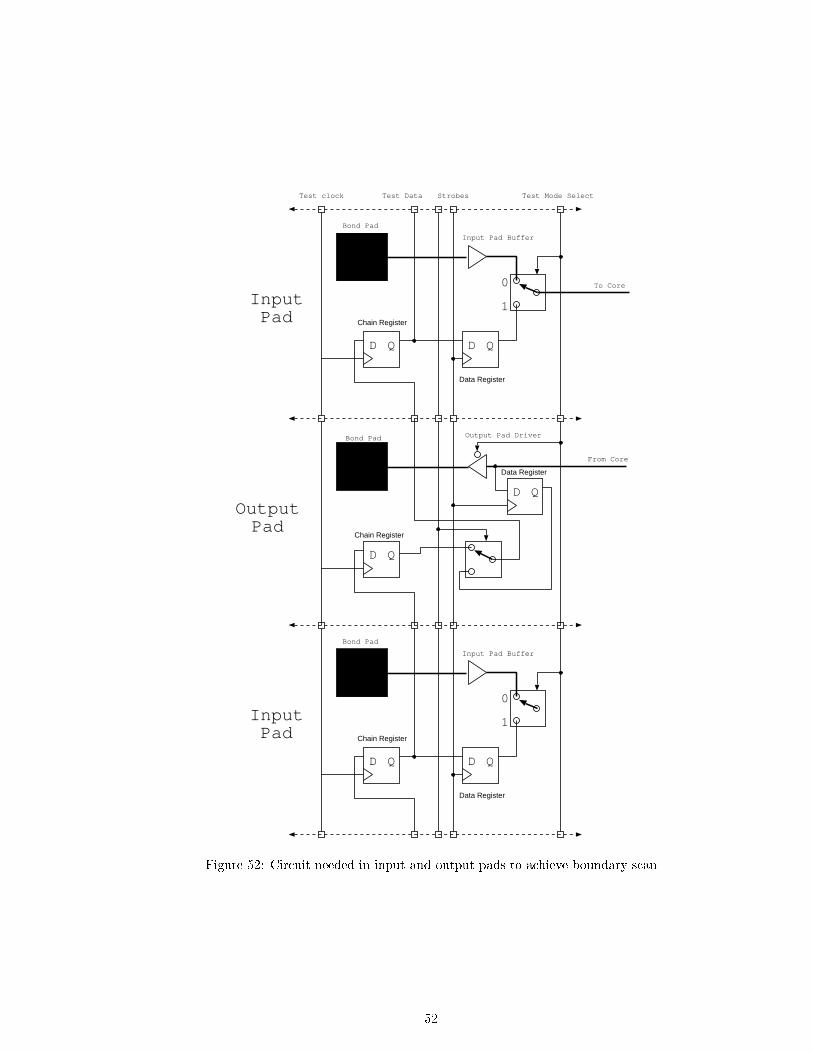
D Q
D Q
Chain Register
Data Register
Output Pad DriverBond Pad
From Core
To Core
OutputPad
D Q D Q
1
0
Bond Pad
Chain Register
Data Register
Input Pad Buffer
InputPad
D Q D Q
1
0
Bond Pad
Chain Register
Data Register
Input Pad Buffer
InputPad
Test clock Test Mode SelectTest Data Strobes
Figure 52: Circuit needed in input and output pads to achieve boundary scan
52

inserted and then generates strobe signals to transfer data in and out of the holding data registersin each pad.
Disadvantage: The main problem with JTAG is that four pins is quite a large number.
Advantage 1: Chips can be tested in place on their �nal circuit board (an in-circuit test).
Advantage 2: If the `chip' is actually a macrocell built into a larger chip or module, then the `chip'can be tested as an autonomous subunit, reusing its own standard test program.
The JTAG port of a chip is becoming used for additional functions:
� device type and serial number,
� in-circuit programming of reusable FPGAs,
� single step debugging of embedded microprocessors.
53

D
Clock
Data inD
Edge Pulse
Figure 53: A simple edge detector
Microprocessor(8 bit generally)
RAM(e.g. 2 Kbytes)
OTPEPROM
(e.g.
8 Kbytes)
ClockOsc
Power Upreset
Programmable IOCounters andTimers
UART
I/O wires OR external bus
Reset capacitorClock
Serial TX and RX
Internal A and D busses
Figure 54: A typical single-chip microcomputer.
6 Further Circuit Structures.
This section introduces some further, fundamental building blocks and includes examples of realproducts. The important points to note are the reasons for the design partition.
6.1 Single Chip Processor
Figure 54 shows the block diagram of a typical single-chip microcomputer. Such devices areavailable in 24, 40 or 80 pin packages and can cost only one or two pounds. The device containsthe whole of a computer, requiring externally only a power supply and some clock and resetcomponents. A number of programmable I/O pins are provided, but generally another basic modeof operation is provided where 24 or so of them turn into the processor address and data bussesfor connection of external devices, such as further RAM or EPROM.
Programming is performed in all of the ways available for ROMs. Generally, uses will use windowedEPROM devices for development and prototypes and ship product with OTP devices.
A Universal asynchronous recevier and transmitter (UART) is normally always provided to helpconnect to RS-232 serial interfaces.
These devices are found everywhere today, from keyboards, clock radios, mice, telephones, carwindow winders, `computer controlled' cassette recorders, cell phones and modems.
54
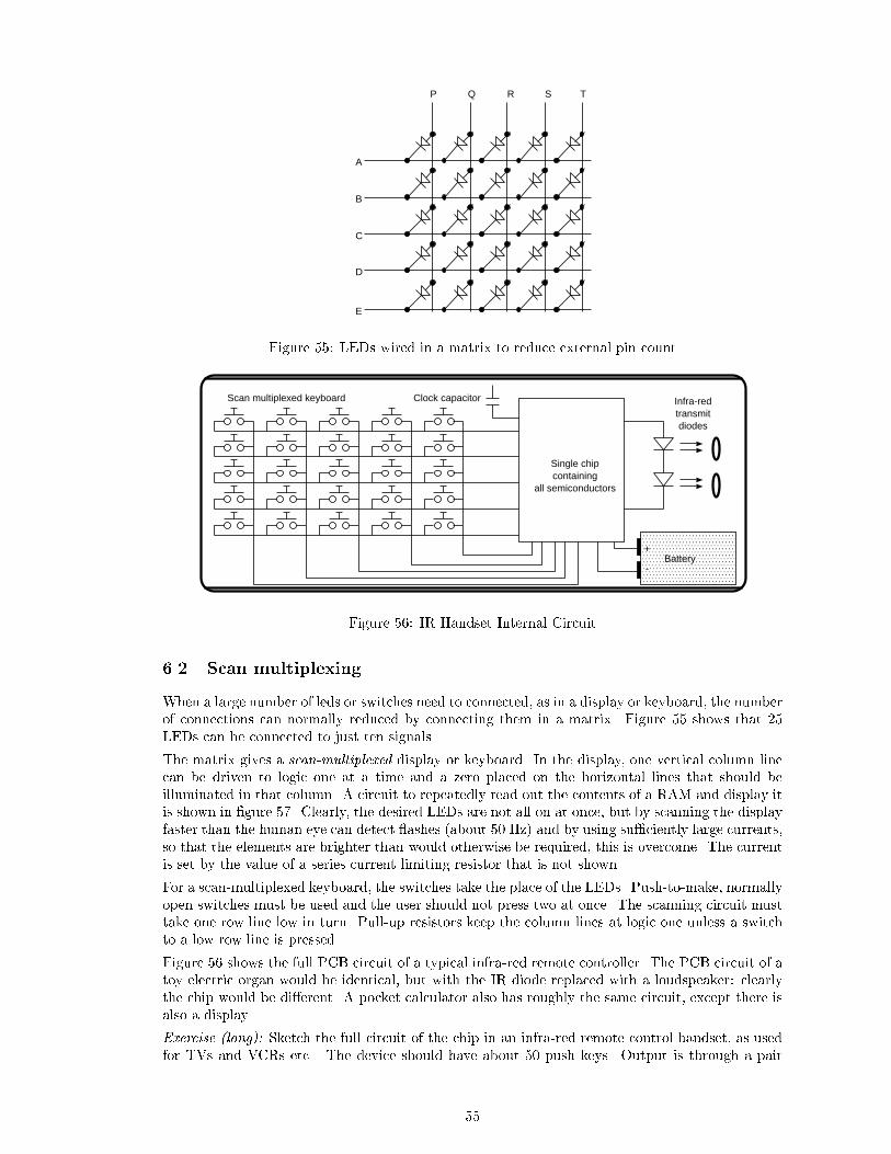
A
B
C
D
E
P Q R S T
Figure 55: LEDs wired in a matrix to reduce external pin count
Battery
Scan multiplexed keyboard
Single chipcontaining
all semiconductors
Clock capacitor Infra-redtransmitdiodes
+
-
Figure 56: IR Handset Internal Circuit
6.2 Scan multiplexing.
When a large number of leds or switches need to connected, as in a display or keyboard, the numberof connections can normally reduced by connecting them in a matrix. Figure 55 shows that 25LEDs can be connected to just ten signals.
The matrix gives a scan-multiplexed display or keyboard. In the display, one vertical column linecan be driven to logic one at a time and a zero placed on the horizontal lines that should beilluminated in that column. A circuit to repeatedly read out the contents of a RAM and display itis shown in �gure 57. Clearly, the desired LEDs are not all on at once, but by scanning the displayfaster than the human eye can detect ashes (about 50 Hz) and by using su�ciently large currents,so that the elements are brighter than would otherwise be required, this is overcome. The currentis set by the value of a series current limiting resistor that is not shown.
For a scan-multiplexed keyboard, the switches take the place of the LEDs. Push-to-make, normallyopen switches must be used and the user should not press two at once. The scanning circuit musttake one row line low in turn. Pull-up resistors keep the column lines at logic one unless a switchto a low row line is pressed.
Figure 56 shows the full PCB circuit of a typical infra-red remote controller. The PCB circuit of atoy electric organ would be identical, but with the IR diode replaced with a loudspeaker: clearlythe chip would be di�erent. A pocket calculator also has roughly the same circuit, except there isalso a display.
Exercise (long): Sketch the full circuit of the chip in an infra-red remote control handset, as usedfor TVs and VCRs etc.. The device should have about 50 push keys. Output is through a pair
55

Pixel
RAM
SCANMULTIPLEXED
DISPLAYMATRIX
N bitCOUNTER
BINARY to UNARYDECODER
Row
Addr
Data lilines(zero for on)
CLOCK
A
D
2^N col lines
One col line islogic one at a time.
Figure 57: Scan multiplex logic for an LED pixel-mapped display
PixelRAM
SCANMULTIPLEXED
DISPLAYMATRIX
N bitCOUNTER
BINARY to UNARYDECODER
Row
A
D
Broadsidetri-statebuffer
Writedata
Write address
WE
Writestrobebar
MUX2 N
Figure 58: Addition of psudo dual-porting logic.
of infra-red transmitting diodes which go on or o� together. The design must include a ROMwhich can be programmed at chip manufacture with the desired sequence of pulses needed. TheROM must contain 16 bits for each key and these bits must be transmitted in turn through theIR diode using a 1 millisecond pulse of light for a zero and a 3 millisecond pulse for a one, with a1 millisecond gap between each pulse.
Exercise: For the IR handset, is it necessary for the clock to be running at all times or only whena key is pressed ? This design aspect will a�ect battery life greatly.
Figure 58 shows how a multiplexor can be added to allow update of the display RAM from aprocessor or similar. The display will brie y show the wrong data while being updated, butthis may be imperceptible to the human. The compromise implied by such psudo-dualporting isaccepted instead of having the cost penalty of truely dual-ported storage. (A second independentport to a RAM or register �le greatly adds to silicon area).
Figure 59 shows the use of a ROM as a function look up table. All electric guitarists use a distortingampli�er and are pernickerty about the exact nature of the distortion. By using a ROM whichcontains a function appropriately distorted from the identity function, any desired distortion canbe achieved.
The input A-to-D circuit samples the input signal at 44100 samples per second, which is the CDsampling frequency. The D-to-A converter on the output reconstructs an analogue signal.
56

A to Dconvertor
Look-up table ROM
D to Aconvertor
16 16
65536 by 16 ROM
Sample clock 44.1 kHz
12 inch speakers
Amplifer
A D
Figure 59: Use of a ROM as a function look-up table.
The analog signals will vary both positively and negatively about zero. Two's complement represen-tations are therefore normally used. Note that to convert from o�set binary to two's complement,one just puts an inverter in the most signi�cant bit.
Exercise: Sketch an alternative circuit using a microprocessor instead of the hardwired solution.What pros and cons do the two approaches have ? How does a processor help with the userinterface?
Figure 60 shows the use of a static RAM to achieve a delay. The counter addresses each locationin turn, and at each location, the old contents are read out before the new contents are put back.
Exercise: The circuit shown produces only a delay. For a true echo e�ect, the original signal mustalso appear at the output. To achieve multiple echos, the output must be fed back to the input atreduced amplitude. Introduce an adder and any additional logic to achieve these results. Use thefact that division by a constant power of two can be achieved by shifting right while leaving thesign bit unchanged.
c DJG 1995, 96, 97, 98.
57

A to Dconvertor
D to Aconvertor
16 16
Amplifer
A
D
Static RAM65536 by 16 bits16 bit
synchronouscounter 16
RAMWE
RAMOE
ADOE
Timing generatorcircuit
ADOE
RAMWE
RAMOE
Derived clock, 44.1 kHz
88.2 kHz
Read cycle Write cycle Read cycle
Clock 88.2
Clock 44.1
RAMWE
RAMOE
Counter Output N-1 N N+1
RAM data pins Old sample replay New sample write
Figure 60: Use of an SRAM to make the delay required for an echo unit.
58

Example Exam Questions
Q. A circuit is needed to divide a very high frequency clock by an average of 21.6. This is tobe done with a counter which accepts a division ratio input to make it divide either by 21 or22. A further counter, made from slower and cheaper logic, is clocked from the output whichgenerates the control signal to the divider, such that the ratio of 21 and 22 counts overall gives thedesired target division ratio. Design it. Prove there are no hazards in your design. Estimate themaximum clock frequency given that the setup time and gate delays of the higher speed logic are1 nanosecond.
Q. An FPGA is to be used to generate a sequencer for disco lights. The FPGA will receive somepulses that are roughly in time with the music (generated by a crude analog circuit or else by amaniac with some switches) and generate 10 or so output signals to control the lights. There arealso some control inputs to select the basic mode (blackout, strobes, dark, light, pattern selectetc.). Sketch a block diagram of the whole system and sketch the circuitry of the FPGA. Is usingan FPGA a good idea?
Q. What is semi-custom design ? When would you use semi-custom? Why might you use anFPGA to prototype a design that is later to be built in semi-custom? What cost di�erence wouldyou expect between an FPGA and a semi-custom versions and why? How might your partition bea�ected by the amount of RAM needed?
Q. A design is required for a wand computer toy. The wand will have a barcode reader whichwill scan barcodes found on groceries and other goods and accumulate credit inside the wand inan unforegable, non-volatile way. A group of young friends, each with their own wand, will beable to compete against each other, gathering points from each item scanned, with more points forrare/valuable goods. Design the wand, including its display and controls and a method for wandsto connect to each other to exchange/swap barcode sightings.
59


![BIBLIOGRAPHY FOR THE LIST OF LISTS [04/01/2012]s3.amazonaws.com/.../files/2012/08/Bibliography-for-the-List-of-Lists… · BIBLIOGRAPHY FOR THE LIST OF LISTS [04/01/2012] ANNUALS:](https://img.dokumen.tips/doc/110x75/5f0288897e708231d404bc94/bibliography-for-the-list-of-lists-04012012s3-bibliography-for-the-list-of.jpg)


![NoodleTools Create a [bibliography, source list…] *](https://img.dokumen.tips/doc/110x75/56816753550346895ddc04f9/noodletools-create-a-bibliography-source-list-.jpg)


![Bibliography Milorad Dusic - List of Publications and Lectures · 2015. 9. 30. · Bibliography Milorad Dusic - List of Publications and Lectures [1] Dusic, M., The measurement of](https://img.dokumen.tips/doc/110x75/5fbeb3590e6fa8270a5d9a30/bibliography-milorad-dusic-list-of-publications-and-lectures-2015-9-30-bibliography.jpg)