Embed Size (px)
Citation preview
Precision Low Noise, Low InputBias Current Operational Amplifiers
Data Sheet OP1177/OP2177/OP4177
Rev. H Document Feedback Information furnished by Analog Devices is believed to be accurate and reliable. However, no responsibility is assumed by Analog Devices for its use, nor for any infringements of patents or other rights of third parties that may result from its use. Specifications subject to change without notice. No license is granted by implication or otherwise under any patent or patent rights of Analog Devices. Trademarks and registered trademarks are the property of their respective owners.
One Technology Way, P.O. Box 9106, Norwood, MA 02062-9106, U.S.A. Tel: 781.329.4700 ©2001–2018 Analog Devices, Inc. All rights reserved. Technical Support www.analog.com
FEATURES Low offset voltage: 60 μV maximum Very low offset voltage drift: 0.7 μV/°C maximum Low input bias current: 2 nA maximum Low noise: 8 nV/√Hz typical CMRR, PSRR, and AVO > 120 dB minimum Low supply current: 400 μA per amplifier Dual supply operation: ±2.5 V to ±15 V Unity-gain stable No phase reversal Inputs internally protected beyond supply voltage
APPLICATIONS Wireless base station control circuits Optical network control circuits Instrumentation Sensors and controls
Thermocouples Resistor thermal detectors (RTDs) Strain bridges Shunt current measurements
Precision filters
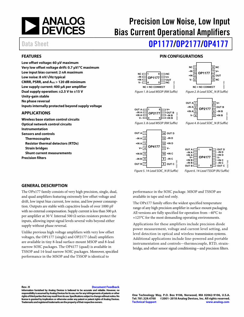
PIN CONFIGURATIONS
–IN+INV–
V+
NC
NC1 8
OP1177NC
OUT
NC = NO CONNECT
4 5
0262
7-00
1
1
2
3
4
8
7
6
5
–IN
V–
+IN
V+
OUT
NC
NC
NC
NC = NO CONNECT
OP1177
0262
7-00
2
Figure 1. 8-Lead MSOP (RM Suffix) Figure 2. 8-Lead SOIC_N (R Suffix)
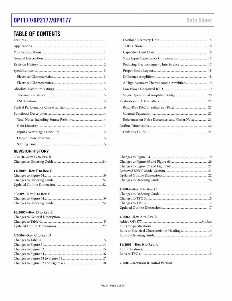
–IN A+IN A
V–
OUT B
+IN B
V+1 8
OP2177OUT A
–IN B4 5
0262
7-00
3
1
2
3
4
8
7
6
5
–IN A
V–
+IN A
OUT B
–IN B
V+
+IN B
OUT A
OP2177
0262
7-00
4
Figure 3. 8-Lead MSOP (RM Suffix) Figure 4. 8-Lead SOIC_N (R Suffix)
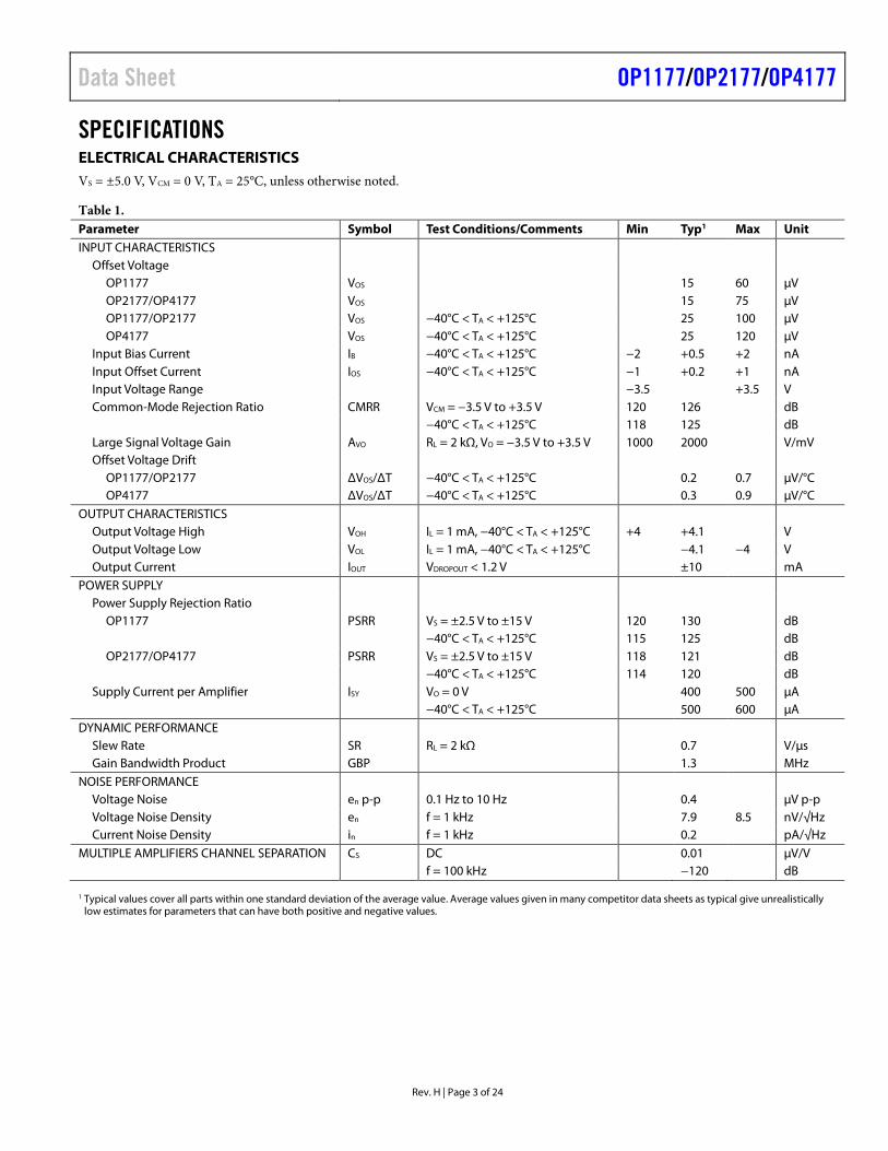
OUT B 7 8
+IN B 5 10
–IN B 6 9
V+ 4 11
–IN A 2 13
+IN A 3 12
OUT A 1 14
OUT C
+IN C
–IN C
V–
–IN D
+IN D
OUT D
OP4177
0262
7-00
5
OUT A–IN A+IN A
V++IN B–IN B
OUT B
–IN D+IN DV–
OUT D
–IN COUT C
+IN C
14
8
1
7
OP4177
0262
7-00
6
Figure 5. 14-Lead SOIC_N (R Suffix) Figure 6. 14-Lead TSSOP (RU Suffix)
GENERAL DESCRIPTION The OPx177 family consists of very high precision, single, dual, and quad amplifiers featuring extremely low offset voltage and drift, low input bias current, low noise, and low power consump-tion. Outputs are stable with capacitive loads of over 1000 pF with no external compensation. Supply current is less than 500 μA per amplifier at 30 V. Internal 500 Ω series resistors protect the inputs, allowing input signal levels several volts beyond either supply without phase reversal.
Unlike previous high voltage amplifiers with very low offset voltages, the OP1177 (single) and OP2177 (dual) amplifiers are available in tiny 8-lead surface-mount MSOP and 8-lead narrow SOIC packages. The OP4177 (quad) is available in TSSOP and 14-lead narrow SOIC packages. Moreover, specified performance in the MSOP and the TSSOP is identical to
performance in the SOIC package. MSOP and TSSOP are available in tape and reel only.
The OPx177 family offers the widest specified temperature range of any high precision amplifier in surface-mount packaging. All versions are fully specified for operation from −40°C to +125°C for the most demanding operating environments.
Applications for these amplifiers include precision diode power measurement, voltage and current level setting, and level detection in optical and wireless transmission systems. Additional applications include line-powered and portable instrumentation and controls—thermocouple, RTD, strain-bridge, and other sensor signal conditioning—and precision filters.
OP1177/OP2177/OP4177 Data Sheet
Rev. H | Page 2 of 24
TABLE OF CONTENTS Features .............................................................................................. 1 Applications ....................................................................................... 1 Pin Configurations ........................................................................... 1 General Description ......................................................................... 1 Revision History ............................................................................... 2 Specifications ..................................................................................... 3
Electrical Characteristics ............................................................. 3 Electrical Characteristics ............................................................. 4
Absolute Maximum Ratings ............................................................ 5 Thermal Resistance ...................................................................... 5 ESD Caution .................................................................................. 5
Typical Performance Characteristics ............................................. 6 Functional Description .................................................................. 14
Total Noise-Including Source Resistors................................... 14 Gain Linearity ............................................................................. 14 Input Overvoltage Protection ................................................... 15 Output Phase Reversal ............................................................... 15 Settling Time ............................................................................... 15
Overload Recovery Time .......................................................... 15 THD + Noise ............................................................................... 16 Capacitive Load Drive ............................................................... 16 Stray Input Capacitance Compensation .................................. 17 Reducing Electromagnetic Interference .................................. 17 Proper Board Layout .................................................................. 18 Difference Amplifiers ................................................................ 18 A High Accuracy Thermocouple Amplifier ........................... 19 Low Power Linearized RTD ...................................................... 19 Single Operational Amplifier Bridge ....................................... 20
Realization of Active Filters .......................................................... 21 Band-Pass KRC or Sallen-Key Filter ........................................ 21 Channel Separation .................................................................... 21 References on Noise Dynamics and Flicker Noise ............... 21
Outline Dimensions ....................................................................... 22 Ordering Guide .......................................................................... 24
REVISION HISTORY 9/2018—Rev. G to Rev. H Changes to Ordering Guide .......................................................... 24 11/2009—Rev. F to Rev. G Changes to Figure 64 ...................................................................... 19 Changes to Ordering Guide .......................................................... 24 Updated Outline Dimensions ....................................................... 22 5/2009—Rev. E to Rev. F Changes to Figure 64 ...................................................................... 19 Changes to Ordering Guide .......................................................... 24 10/2007—Rev. D to Rev. E Changes to General Description .................................................... 1 Changes to Table 4 ............................................................................ 5 Updated Outline Dimensions ....................................................... 22 7/2006—Rev. C to Rev. D Changes to Table 4 ............................................................................ 5 Changes to Figure 51 ...................................................................... 14 Changes to Figure 52 ...................................................................... 15 Changes to Figure 54 ...................................................................... 16 Changes to Figure 58 to Figure 61 ................................................ 17 Changes to Figure 62 and Figure 63 ............................................. 18
Changes to Figure 64 ...................................................................... 19 Changes to Figure 65 and Figure 66 ............................................ 20 Changes to Figure 67 and Figure 68 ............................................ 21 Removed SPICE Model Section ................................................... 21 Updated Outline Dimensions ....................................................... 22 Changes to Ordering Guide .......................................................... 24 4/2004—Rev. B to Rev. C Changes to Ordering Guide ............................................................. 4 Changes to TPC 6 .............................................................................. 5 Changes to TPC 26 ............................................................................ 7 Updated Outline Dimensions ....................................................... 17 4/2002—Rev. A to Rev. B Added OP4177 ......................................................................... Global Edits to Specifications ....................................................................... 2 Edits to Electrical Characteristics Headings .................................. 4 Edits to Ordering Guide ................................................................... 4 11/2001—Rev. 0 to Rev. A Edit to Features .................................................................................. 1 Edits to TPC 6 ................................................................................... 5 7/2001—Revision 0: Initial Version
Data Sheet OP1177/OP2177/OP4177
Rev. H | Page 3 of 24
SPECIFICATIONS ELECTRICAL CHARACTERISTICS VS = ±5.0 V, VCM = 0 V, TA = 25°C, unless otherwise noted.
Table 1. Parameter Symbol Test Conditions/Comments Min Typ1 Max Unit INPUT CHARACTERISTICS
Offset Voltage OP1177 VOS 15 60 μV OP2177/OP4177 VOS 15 75 μV OP1177/OP2177 VOS −40°C < TA < +125°C 25 100 μV OP4177 VOS −40°C < TA < +125°C 25 120 μV
Input Bias Current IB −40°C < TA < +125°C −2 +0.5 +2 nA Input Offset Current IOS −40°C < TA < +125°C −1 +0.2 +1 nA Input Voltage Range −3.5 +3.5 V Common-Mode Rejection Ratio CMRR VCM = −3.5 V to +3.5 V 120 126 dB −40°C < TA < +125°C 118 125 dB Large Signal Voltage Gain AVO RL = 2 kΩ, VO = −3.5 V to +3.5 V 1000 2000 V/mV Offset Voltage Drift
OP1177/OP2177 ΔVOS/ΔT −40°C < TA < +125°C 0.2 0.7 μV/°C OP4177 ΔVOS/ΔT −40°C < TA < +125°C 0.3 0.9 μV/°C
OUTPUT CHARACTERISTICS Output Voltage High VOH IL = 1 mA, −40°C < TA < +125°C +4 +4.1 V Output Voltage Low VOL IL = 1 mA, −40°C < TA < +125°C −4.1 −4 V Output Current IOUT VDROPOUT < 1.2 V ±10 mA
POWER SUPPLY Power Supply Rejection Ratio
OP1177 PSRR VS = ±2.5 V to ±15 V 120 130 dB −40°C < TA < +125°C 115 125 dB OP2177/OP4177 PSRR VS = ±2.5 V to ±15 V 118 121 dB
−40°C < TA < +125°C 114 120 dB Supply Current per Amplifier ISY VO = 0 V 400 500 μA
−40°C < TA < +125°C 500 600 μA DYNAMIC PERFORMANCE
Slew Rate SR RL = 2 kΩ 0.7 V/μs Gain Bandwidth Product GBP 1.3 MHz
NOISE PERFORMANCE Voltage Noise en p-p 0.1 Hz to 10 Hz 0.4 μV p-p Voltage Noise Density en f = 1 kHz 7.9 8.5 nV/√Hz Current Noise Density in f = 1 kHz 0.2 pA/√Hz
MULTIPLE AMPLIFIERS CHANNEL SEPARATION CS DC 0.01 μV/V f = 100 kHz −120 dB 1 Typical values cover all parts within one standard deviation of the average value. Average values given in many competitor data sheets as typical give unrealistically
low estimates for parameters that can have both positive and negative values.
OP1177/OP2177/OP4177 Data Sheet
Rev. H | Page 4 of 24
ELECTRICAL CHARACTERISTICS VS = ±15 V, VCM = 0 V, TA = 25°C, unless otherwise noted.
Table 2. Parameter Symbol Conditions Min Typ1 Max Unit INPUT CHARACTERISTICS
Offset Voltage OP1177 VOS 15 60 μV OP2177/OP4177 VOS 15 75 μV OP1177/OP2177 VOS −40°C < TA < +125°C 25 100 μV OP4177 VOS −40°C < TA < +125°C 25 120 μV
Input Bias Current IB −40°C < TA < +125°C −2 +0.5 +2 nA Input Offset Current IOS −40°C < TA < +125°C −1 +0.2 +1 nA Input Voltage Range −13.5 +13.5 V Common-Mode Rejection Ratio CMRR VCM = −13.5 V to +13.5 V, −40°C < TA < +125°C 120 125 dB Large Signal Voltage Gain AVO RL = 2 kΩ, VO = –13.5 V to +13.5 V 1000 3000 V/mV Offset Voltage Drift
OP1177/OP2177 ΔVOS/ΔT −40°C < TA < +125°C 0.2 0.7 μV/°C OP4177 ΔVOS/ΔT −40°C < TA < +125°C 0.3 0.9 μV/°C
OUTPUT CHARACTERISTICS Output Voltage High VOH IL = 1 mA, −40°C < TA < +125°C +14 +14.1 V Output Voltage Low VOL IL = 1 mA, −40°C < TA < +125°C −14.1 −14 V Output Current IOUT VDROPOUT < 1.2 V ±10 mA Short-Circuit Current ISC ±25 mA
POWER SUPPLY Power Supply Rejection Ratio
OP1177 PSRR VS = ±2.5 V to ±15 V 120 130 dB −40°C < TA < +125°C 115 125 dB OP2177/OP4177 PSRR VS = ±2.5 V to ±15 V 118 121 dB
−40°C < TA < +125°C 114 120 dB Supply Current per Amplifier ISY VO = 0 V 400 500 μA −40°C < TA < +125°C 500 600 μA
DYNAMIC PERFORMANCE Slew Rate SR RL = 2 kΩ 0.7 V/μs Gain Bandwidth Product GBP 1.3 MHz
NOISE PERFORMANCE Voltage Noise en p-p 0.1 Hz to 10 Hz 0.4 μV p-p Voltage Noise Density en f = 1 kHz 7.9 8.5 nV/√Hz Current Noise Density in f = 1 kHz 0.2 pA/√Hz
MULTIPLE AMPLIFIERS CHANNEL SEPARATION CS DC 0.01 μV/V f = 100 kHz −120 dB 1 Typical values cover all parts within one standard deviation of the average value. Average values given in many competitor data sheets as typical give unrealistically
low estimates for parameters that can have both positive and negative values.
Data Sheet OP1177/OP2177/OP4177
Rev. H | Page 5 of 24
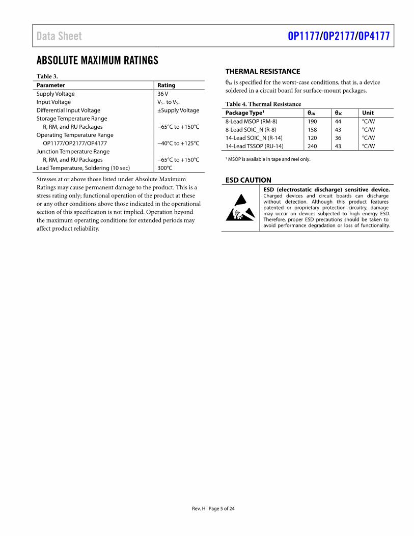
ABSOLUTE MAXIMUM RATINGS Table 3. Parameter Rating Supply Voltage 36 V Input Voltage VS− to VS+ Differential Input Voltage ±Supply Voltage Storage Temperature Range
R, RM, and RU Packages −65°C to +150°C Operating Temperature Range
OP1177/OP2177/OP4177 −40°C to +125°C Junction Temperature Range
R, RM, and RU Packages −65°C to +150°C Lead Temperature, Soldering (10 sec) 300°C
Stresses at or above those listed under Absolute Maximum Ratings may cause permanent damage to the product. This is a stress rating only; functional operation of the product at these or any other conditions above those indicated in the operational section of this specification is not implied. Operation beyond the maximum operating conditions for extended periods may affect product reliability.
THERMAL RESISTANCE
θJA is specified for the worst-case conditions, that is, a device soldered in a circuit board for surface-mount packages.
Table 4. Thermal Resistance Package Type1 θJA θJC Unit 8-Lead MSOP (RM-8) 190 44 °C/W 8-Lead SOIC_N (R-8) 158 43 °C/W 14-Lead SOIC_N (R-14) 120 36 °C/W 14-Lead TSSOP (RU-14) 240 43 °C/W 1 MSOP is available in tape and reel only.
ESD CAUTION
OP1177/OP2177/OP4177 Data Sheet
Rev. H | Page 6 of 24
TYPICAL PERFORMANCE CHARACTERISTICS
INPUT OFFSETVOLTAGE (µV)
NU
MB
ER O
F A
MPL
IFIE
RS
45
40
35
30
25
20
15
10
5
–30 –20 –10 0 10 20 30 400
50
–40
VSY = ±15V
0262
7-00
7
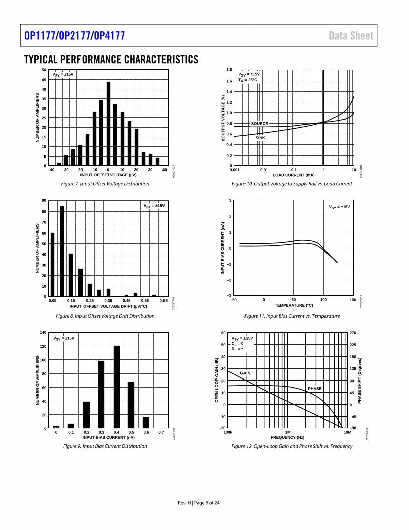
Figure 7. Input Offset Voltage Distribution
INPUT OFFSET VOLTAGE DRIFT (µV/°C)
NU
MB
ER O
F A
MPL
IFIE
RS
80
70
60
50
40
30
20
10
0.15 0.25 0.35 0.45 0.55 0.650
90
0.05
VSY = ±15V
0262
7-00
8
Figure 8. Input Offset Voltage Drift Distribution
INPUT BIAS CURRENT (nA)
NU
MB
ER O
F A
MPL
IFIE
RS
120
100
80
60
40
20
0.1 0.2 0.3 0.4 0.5 0.6 0.70
140
0
VSY = ±15V
0262
7-00
9
Figure 9. Input Bias Current Distribution
LOAD CURRENT (mA)
ΔO
UTP
UT
VOLT
AG
E (V
)
0.01 0.1 1
1.6
1.4
1.2
1.0
0.8
0.6
0.4
0.2
0
1.8
0.001 10
SOURCE
SINK
VSY = ±15VTA = 25°C
0262
7-01
0
Figure 10. Output Voltage to Supply Rail vs. Load Current
TEMPERATURE (°C)
VSY = ±15V
INPU
T B
IAS
CU
RR
ENT
(nA
)2
1
0
–1
–2
0 50 100
3
–3–50 150
0262
7-01
1
Figure 11. Input Bias Current vs. Temperature
FREQUENCY (Hz)
PHA
SE S
HIF
T (D
egre
es)
OPE
N-L
OO
P G
AIN
(dB
)
1M
50
40
30
20
10
0
–10
60
–20100k 10M
225
180
135
90
45
0
–45
270
–90
GAIN
PHASE
VSY = ±15VCL = 0RL = ∞
0262
7-01
2
Figure 12. Open-Loop Gain and Phase Shift vs. Frequency
Data Sheet OP1177/OP2177/OP4177
Rev. H | Page 7 of 24
FREQUENCY (Hz)
CL
OS
ED
-LO
OP
GA
IN (
dB
)
10k 100k 1M 10M
100
80
60
40
20
0
–20
–40
–60
120
–801k 100M
VSY = ±15VVIN = 4mV p-pCL = 0RL = ∞
AV = 100
AV = 1
AV = 10
0262
7-01
3
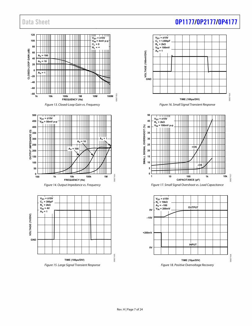
Figure 13. Closed-Loop Gain vs. Frequency
FREQUENCY (Hz)
OU
TP
UT
IM
PE
DA
NC
E (Ω
)
1k 10k 100k 1M
450
400
350
300
250
200
150
100
50
100
500
0
VSY = ±15VVIN = 50mV p-p
AV = 10
AV = 100
AV = 1
0262
7-01
4
Figure 14. Output Impedance vs. Frequency
TIME (100µs/DIV)
VO
LT
AG
E (
1V/D
IV)
GND
VSY = ±15VCL = 300pFRL = 2kΩVIN = 4VAV = 1
0262
7-01
5
Figure 15. Large Signal Transient Response
TIME (100µs/DIV)
VO
LT
AG
E (
100m
V/D
IV)
GND
VSY = ±15VCL = 1,000pFRL = 2kΩVIN = 100mVAV = 1
0262
7-01
6
Figure 16. Small Signal Transient Response
CAPACITANCE (pF)
SM
AL
L S
IGN
AL
OV
ER
SH
OO
T (
%)
10 100 1k1 10k
45
40
35
30
25
20
15
10
5
50
0
+OS
–OS
VSY = ±15VRL = 2kΩVIN = 100mV p-p
0262
7-01
7
Figure 17. Small Signal Overshoot vs. Load Capacitance
TIME (10µs/DIV)
+200mV
0V
–15V
0V
VSY = ±15VRL = 10kΩAV = –100VIN = 200mV
INPUT
OUTPUT
0262
7-01
8
Figure 18. Positive Overvoltage Recovery
OP1177/OP2177/OP4177 Data Sheet
Rev. H | Page 8 of 24
TIME (4µs/DIV)
0V
–200mV
0V
15V
VSY = ±15VRL = 10kΩAV = –100VIN = 200mV
INPUT
OUTPUT
0262
7-01
9
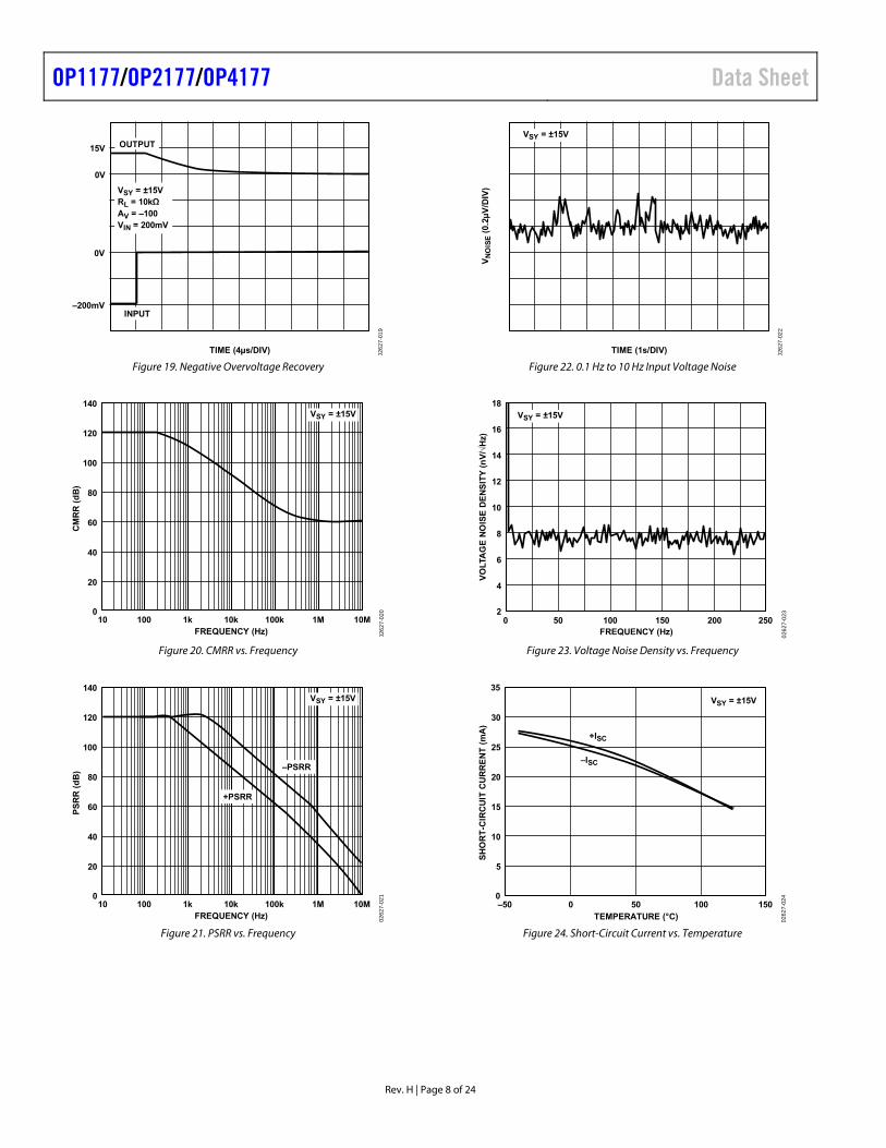
Figure 19. Negative Overvoltage Recovery
FREQUENCY (Hz)
CM
RR
(d
B)
100 1k 10k 100k 1M
120
100
80
60
40
20
140
010 10M
VSY = ±15V
0262
7-02
0
Figure 20. CMRR vs. Frequency
FREQUENCY (Hz)
PS
RR
(d
B)
100 1k 10k 100k 1M
120
100
80
60
40
20
140
010 10M
VSY = ±15V
+PSRR
–PSRR
0262
7-02
1
Figure 21. PSRR vs. Frequency
VN
OIS
E (
0.2µ
V/D
IV)
TIME (1s/DIV)
VSY = ±15V
0262
7-02
2
Figure 22. 0.1 Hz to 10 Hz Input Voltage Noise
FREQUENCY (Hz)
16
14
12
10
8
6
4
18
250 100 150 2000 250
VSY = ±15V
VO
LTA
GE
NO
ISE
DE
NS
ITY
(n
V/√
Hz)
0262
7-02
3
Figure 23. Voltage Noise Density vs. Frequency
SH
OR
T-C
IRC
UIT
CU
RR
EN
T (
mA
)
+ISC
–ISC
TEMPERATURE (°C)
30
25
20
15
10
5
0 50 100
35
0–50 150
VSY = ±15V
0262
7-02
4
Figure 24. Short-Circuit Current vs. Temperature
Data Sheet OP1177/OP2177/OP4177
Rev. H | Page 9 of 24
OU
TPU
T VO
LTA
GE
SWIN
G (V
)
14.40
14.00
14.30
14.05
14.25
14.20
14.15
14.10
14.35
+VOH
–VOL
TEMPERATURE (°C)0 50 100–50 150
VSY = ±15V
0262
7-02
5
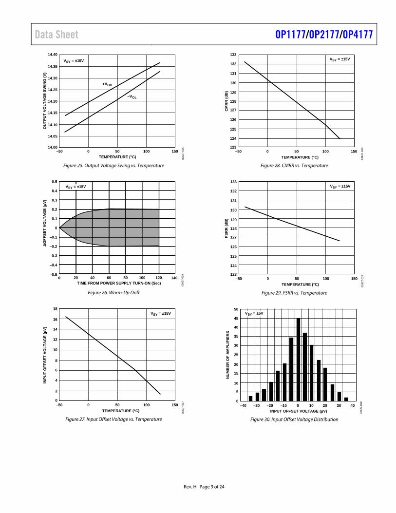
Figure 25. Output Voltage Swing vs. Temperature
TIME FROM POWER SUPPLY TURN-ON (Sec)
ΔO
FFSE
T VO
LTA
GE
(µV)
0.4
0.3
0.2
0.1
0
–0.1
–0.2
–0.3
0.5
–0.5
–0.4
20 40 60 80 100 1200 140
VSY = ±15V02
627-
026
Figure 26. Warm-Up Drift
INPU
T O
FFSE
T VO
LTA
GE
(µV)
0
12
8
4
14
18
2
6
10
16
TEMPERATURE (°C)
VSY = ±15V
0 50 100–50 150
0262
7-02
7
Figure 27. Input Offset Voltage vs. Temperature
CM
RR
(dB
)
123
127
125
128
129
124
126
130
131
132
133
TEMPERATURE (°C)
VSY = ±15V
0 50 100–50 150
0262
7-02
8
Figure 28. CMRR vs. Temperature
PSR
R (d
B)
123
127
125
128
129
124
126
130
131
132
133
TEMPERATURE (°C)
VSY = ±15V
0 50 100–50 150
0262
7-02
9
Figure 29. PSRR vs. Temperature
INPUT OFFSET VOLTAGE (µV)
NU
MB
ER O
F A
MPL
IFIE
RS
50
15
0
45
20
10
5
30
25
40
35
VSY = ±5V
–40 –30 –20 –10 0 10 20 30 40
0262
7-03
0
Figure 30. Input Offset Voltage Distribution
OP1177/OP2177/OP4177 Data Sheet
Rev. H | Page 10 of 24
∆O
UT
PU
T V
OL
TA
GE
(V
)
LOAD CURRENT (mA)
1.4
0.8
0
0.4
0.2
0.6
1.0
1.2
0.01 0.1 1
VSY = ±5VTA = 25°C
SINK
SOURCE
0.001 10
0262
7-03
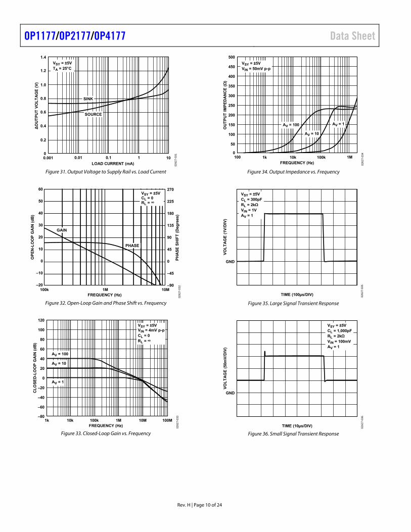
1Figure 31. Output Voltage to Supply Rail vs. Load Current
02
627-
032
FREQUENCY (Hz)
PH
AS
E S
HIF
T (
Deg
rees
)
OP
EN
-LO
OP
GA
IN (
dB
)
1M
50
40
30
20
10
0
–10
60
–20100k 10M
225
180
135
90
45
0
–45
270
–90
GAIN
PHASE
VSY = ±5VCL = 0RL = ∞
Figure 32. Open-Loop Gain and Phase Shift vs. Frequency
FREQUENCY (Hz)
CL
OS
ED
-LO
OP
GA
IN (
dB
)
10k 100k 1M 10M
100
80
60
40
20
0
–20
–40
–60
120
–801k 100M
VSY = ±5VVIN = 4mV p-pCL = 0RL = ∞
AV = 100
AV = 1
AV = 10
0262
7-03
3
Figure 33. Closed-Loop Gain vs. Frequency
FREQUENCY (Hz)
OU
TP
UT
IM
PE
DA
NC
E (Ω
)
1k 10k 100k100 1M
450
400
350
300
250
200
150
100
50
500
0
VSY = ±5VVIN = 50mV p-p
AV = 100 AV = 1
AV = 10
0262
7-03
4
Figure 34. Output Impedance vs. Frequency
TIME (100µs/DIV)
VO
LT
AG
E (
1V/D
IV)
GND
VSY = ±5VCL = 300pFRL = 2kΩVIN = 1VAV = 1
0262
7-03
5
Figure 35. Large Signal Transient Response
TIME (10µs/DIV)
VO
LT
AG
E (
50m
V/D
IV)
GND
VSY = ±5VCL = 1,000pFRL = 2kΩVIN = 100mVAV = 1
0262
7-03
6
Figure 36. Small Signal Transient Response
Data Sheet OP1177/OP2177/OP4177
Rev. H | Page 11 of 24
CAPACITANCE (pF)
SM
AL
L S
IGN
AL
OV
ER
SH
OO
T (
%)
10 100 1k1 10k
45
40
35
30
25
20
15
10
5
50
0
+OS
–OS
VSY = ±5VRL = 2kΩVIN = 100mV
0262
7-03
7
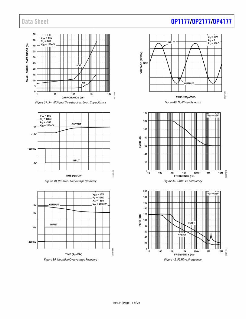
Figure 37. Small Signal Overshoot vs. Load Capacitance
TIME (4µs/DIV)
+200mV
0V
–15V
0V
VSY = ±5VRL = 10kΩAV = –100VIN = 200mV
INPUT
OUTPUT
0262
7-03
8
Figure 38. Positive Overvoltage Recovery
TIME (4µs/DIV)
0V
–200mV
0V
5V
VSY = ±5VRL = 10kΩAV = –100VIN = 200mV
INPUT
OUTPUT
0262
7-03
9
Figure 39. Negative Overvoltage Recovery
TIME (200µs/DIV)
VO
LT
AG
E (
2V/D
IV)
GND
VS = ±5VAV = 1RL = 10kΩINPUT
OUTPUT
0262
7-04
0
Figure 40. No Phase Reversal
FREQUENCY (Hz)
CM
RR
(d
B)
100 1k 10k 100k 1M
120
100
80
60
40
20
140
010 10M
VSY = ±5V
0262
7-04
1
Figure 41. CMRR vs. Frequency
FREQUENCY (Hz)
PS
RR
(d
B)
100 1k 10k 100k 1M
160
120
80
40
200
010 10M
VSY = ±5V
140
100
60
20
180
+PSRR
–PSRR02
627-
042
Figure 42. PSRR vs. Frequency
OP1177/OP2177/OP4177 Data Sheet
Rev. H | Page 12 of 24
VN
OIS
E (
0.2µ
V/D
IV)
TIME (1s/DIV)
VSY = ±5V
0262
7-04
3
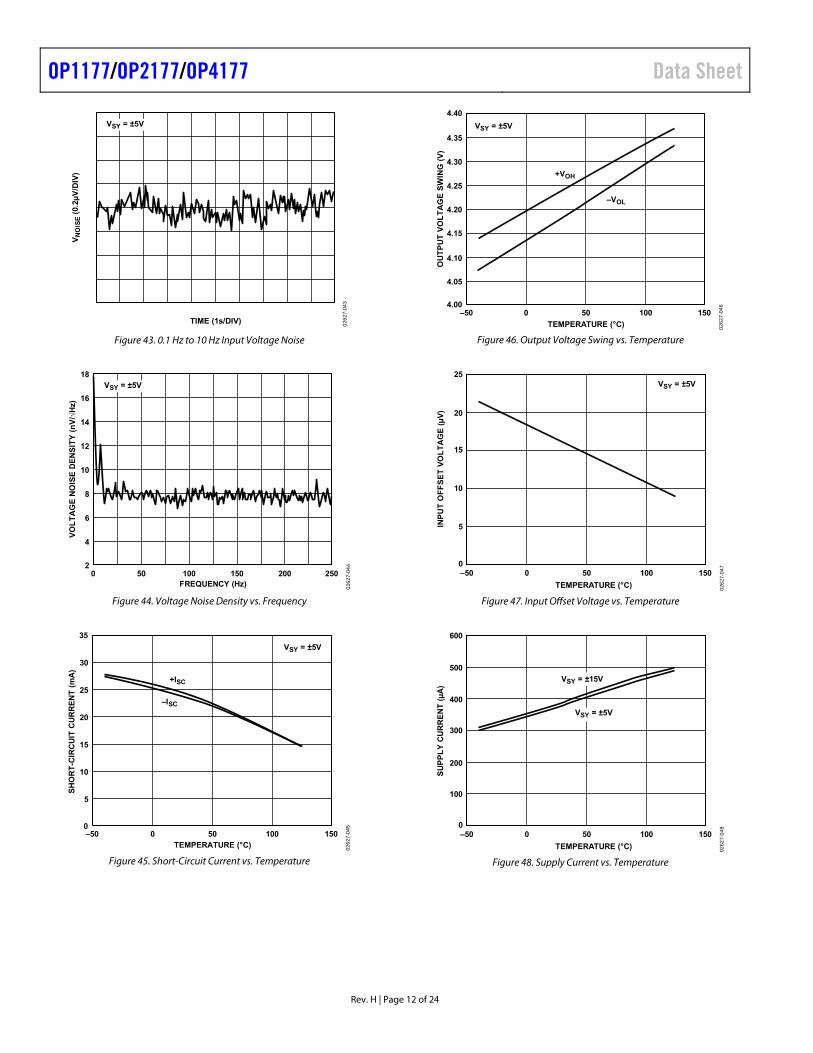
Figure 43. 0.1 Hz to 10 Hz Input Voltage Noise
FREQUENCY (Hz)
16
14
12
10
8
6
4
18
250 100 150 2000 250
VSY = ±5V
VO
LT
AG
E N
OIS
E D
EN
SIT
Y (
nV
/√H
z)
0262
7-04
4
Figure 44. Voltage Noise Density vs. Frequency
SH
OR
T-C
IRC
UIT
CU
RR
EN
T (
mA
)
+ISC
–ISC
TEMPERATURE (°C)
30
25
20
15
10
5
0 50 100
35
0–50 150
VSY = ±5V
0262
7-04
5
Figure 45. Short-Circuit Current vs. Temperature
OU
TP
UT
VO
LT
AG
E S
WIN
G (
V)
4.40
4.00
4.30
4.05
4.25
4.20
4.15
4.10
4.35
+VOH
–VOL
TEMPERATURE (°C)
0 50 100–50 150
VSY = ±5V
0262
7-04
6
Figure 46. Output Voltage Swing vs. Temperature
INP
UT
OF
FS
ET
VO
LT
AG
E (
µV
)
0
10
5
20
25
15
TEMPERATURE (°C)
VSY = ±5V
0 50 100–50 150
0262
7-04
7
Figure 47. Input Offset Voltage vs. Temperature
SU
PP
LY
CU
RR
EN
T (
µA
)
0
300
200
500
600
400
TEMPERATURE (°C)
0 50 100–50 150
100
VSY = ±5V
VSY = ±15V
0262
7-04
8
Figure 48. Supply Current vs. Temperature
Data Sheet OP1177/OP2177/OP4177
Rev. H | Page 13 of 24
SUPP
LY C
UR
REN
T (µ
A)
0
300
200
100
350
450
50
150
250
400
SUPPLY VOLTAGE (V)5 10 150 20 25 30 35
TA = 25°C
0262
7-04
9
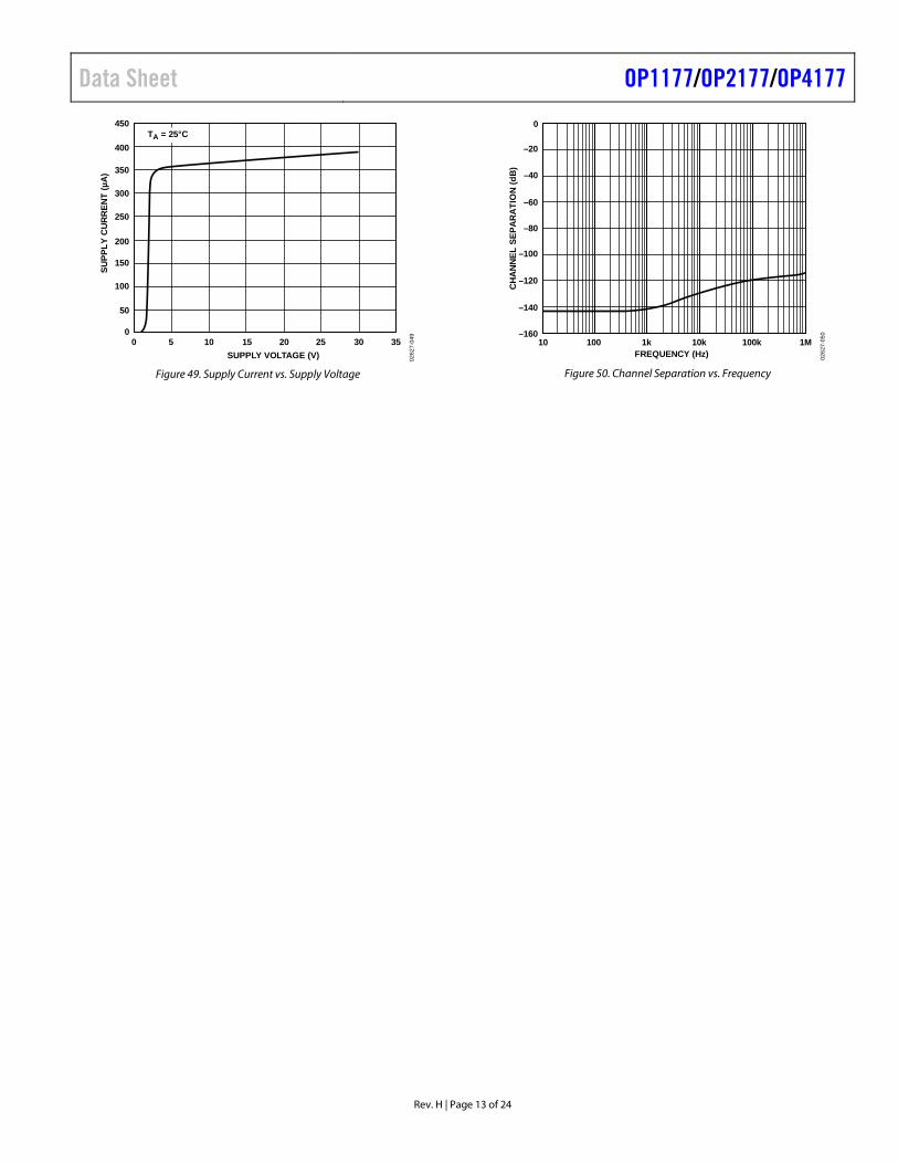
Figure 49. Supply Current vs. Supply Voltage
FREQUENCY (Hz)
CH
AN
NEL
SEP
AR
ATI
ON
(dB
)
100 1k 10k 100k
–20
–40
–60
–80
–100
–120
–140
0
–16010 1M
0262
7-05
0
Figure 50. Channel Separation vs. Frequency
OP1177/OP2177/OP4177 Data Sheet
Rev. H | Page 14 of 24
FUNCTIONAL DESCRIPTION The OPx177 series is the fourth generation of Analog Devices, Inc., industry-standard OP07 amplifier family. OPx177 is a high precision, low noise operational amplifier with a combination of extremely low offset voltage and very low input bias currents. Unlike JFET amplifiers, the low bias and offset currents are relatively insensitive to ambient temperatures, even up to 125°C.
Analog Devices proprietary process technology and linear design expertise has produced a high voltage amplifier with superior performance to the OP07, OP77, and OP177 in a tiny MSOP 8lead package. Despite its small size, the OPx177 offers numerous improvements, including low wideband noise, very wide input and output voltage range, lower input bias current, and complete freedom from phase inversion.
OPx177 has a specified operating temperature range as wide as any similar device in a plastic surface-mount package. This is increasingly important as PCB and overall system sizes continue to shrink, causing internal system temperatures to rise. Power consumption is reduced by a factor of four from the OP177, and bandwidth and slew rate increase by a factor of two. The low power dissipation and very stable performance vs. temperature also act to reduce warmup drift errors to insignificant levels.
Open-loop gain linearity under heavy loads is superior to compet-itive parts, such as the OPA277, improving dc accuracy and reducing distortion in circuits with high closed-loop gains. Inputs are internally protected from overvoltage conditions referenced to either supply rail.
Like any high performance amplifier, maximum performance is achieved by following appropriate circuit and PCB guidelines. The following sections provide practical advice on getting the most out of the OPx177 under a variety of application conditions.
TOTAL NOISE-INCLUDING SOURCE RESISTORS The low input current noise and input bias current of the OPx177 make it useful for circuits with substantial input source resistance. Input offset voltage increases by less than 1 μV maximum per 500 Ω of source resistance.
The total noise density of the OPx177 is
SSnnTOTALn kTRRiee 42 2,
where: en is the input voltage noise density. in is the input current noise density. RS is the source resistance at the noninverting terminal. k is Boltzmann’s constant (1.38 × 10⁻²³ J/K). T is the ambient temperature in Kelvin (T = 273 + temperature in degrees Celsius).
For RS < 3.9 kΩ, en dominates and
en,TOTAL ≈ en
For 3.9 kΩ < RS < 412 kΩ, voltage noise of the amplifier, the current noise of the amplifier translated through the source resistor, and the thermal noise from the source resistor all contribute to the total noise.
For RS > 412 kΩ, the current noise dominates and
en,TOTAL ≈ inRS
The total equivalent rms noise over a specific bandwidth is expressed as
BWee TOTALnn ,
where BW is the bandwidth in hertz.
The preceding analysis is valid for frequencies larger than 50 Hz. When considering lower frequencies, flicker noise (also known as 1/f noise) must be taken into account.
For a reference on noise calculations, refer to the Band-Pass KRC or Sallen-Key Filter section.
GAIN LINEARITY Gain linearity reduces errors in closed-loop configurations. The straighter the gain curve, the lower the maximum error over the input signal range. This is especially true for circuits with high closed-loop gains.
The OP1177 has excellent gain linearity even with heavy loads, as shown in Figure 51. Compare its performance to the OPA277, shown in Figure 52. Both devices are measured under identical conditions, with RL = 2 kΩ. The OP2177 (dual) has virtually no distortion at lower voltages. Compared to the OPA277 at several supply voltages and various loads, OP1177 performance far exceeds that of its counterpart.
(5V/DIV)
OP1177
(10µ
V/D
IV)
VSY = ±15VRL = 2kΩ
0262
7-05
1
Figure 51. Gain Linearity

Data Sheet OP1177/OP2177/OP4177
Rev. H | Page 15 of 24
(5V/DIV)
OPA277
VSY = ±15VRL = 2kΩ
(10µ
V/D
IV)
0262
7-05
2
Figure 52. Gain Linearity
INPUT OVERVOLTAGE PROTECTION When input voltages exceed the positive or negative supply voltage, most amplifiers require external resistors to protect them from damage.
The OPx177 has internal protective circuitry that allows voltages as high as 2.5 V beyond the supplies to be applied at the input of either terminal without any harmful effects.
Use an additional resistor in series with the inputs if the voltage exceeds the supplies by more than 2.5 V. The value of the resistor can be determined from the formula
5 mA500
IN S
S
V VR
With the OPx177 low input offset current of <1 nA maximum, placing a 5 kΩ resistor in series with both inputs adds less than 5 μV to input offset voltage and has a negligible impact on the overall noise performance of the circuit.
5 kΩ protects the inputs to more than 27 V beyond either supply. Refer to the THD + Noise section for additional information on noise vs. source resistance.
OUTPUT PHASE REVERSAL Phase reversal is defined as a change of polarity in the amplifier transfer function. Many operational amplifiers exhibit phase reversal when the voltage applied to the input is greater than the maximum common-mode voltage. In some instances, this can cause permanent damage to the amplifier. In feedback loops, it can result in system lockups or equipment damage. The OPx177 is immune to phase reversal problems even at input voltages beyond the supplies.
VSY = 10VAV = 1
TIME (400µs/DIV)
VIN
VOUT
VO
LTA
GE
(5V
/DIV
)
0262
7-05
3
Figure 53. No Phase Reversal
SETTLING TIME Settling time is defined as the time it takes an amplifier output to reach and remain within a percentage of its final value after application of an input pulse. It is especially important in measure-ment and control circuits in which amplifiers buffer ADC inputs or DAC outputs.
To minimize settling time in amplifier circuits, use proper bypassing of power supplies and an appropriate choice of circuit components. Resistors should be metal film types, because they have less stray capacitance and inductance than their wire-wound counterparts. Capacitors should be polystyrene or polycarbonate types to minimize dielectric absorption.
The leads from the power supply should be kept as short as possible to minimize capacitance and inductance. The OPx177 has a settling time of about 45 μs to 0.01% (1 mV) with a 10 V step applied to the input in a noninverting unity gain.
OVERLOAD RECOVERY TIME Overload recovery is defined as the time it takes the output voltage of an amplifier to recover from a saturated condition to its linear response region. A common example is one in which the output voltage demanded by the transfer function of the circuit lies beyond the maximum output voltage capability of the amplifier. A 10 V input applied to an amplifier in a closed-loop gain of 2 demands an output voltage of 20 V. This is beyond the output voltage range of the OPx177 when operating at ±15 V supplies and forces the output into saturation.
Recovery time is important in many applications, particularly where the operational amplifier must amplify small signals in the presence of large transient voltages.
OP1177/OP2177/OP4177 Data Sheet
Rev. H | Page 16 of 24
OP11776
72
3
4
V+
V–
R2100kΩ
VOUT
10kΩ
R11kΩ
+–
200mV
0262
7-05
4
Figure 54. Test Circuit for Overload Recovery Time
Figure 18 shows the positive overload recovery time of the OP1177. The output recovers in less than 4 μs after being overdriven by more than 100%.
The negative overload recovery of the OP1177 is 1.4 μs, as seen in Figure 19.
THD + NOISE The OPx177 has very low total harmonic distortion. This indicates excellent gain linearity and makes the OPx177 a great choice for high closed-loop gain precision circuits.
Figure 55 shows that the OPx177 has approximately 0.00025% distortion in unity gain, the worst-case configuration for distortion.
FREQUENCY (Hz)
TH
D +
N (
%)
100 1k
0.001
0.01
20 6k0.0001
0.1
0262
7-05
5
VSY = ±15VRL = 10kΩBW = 22kHz
Figure 55. THD + N vs. Frequency
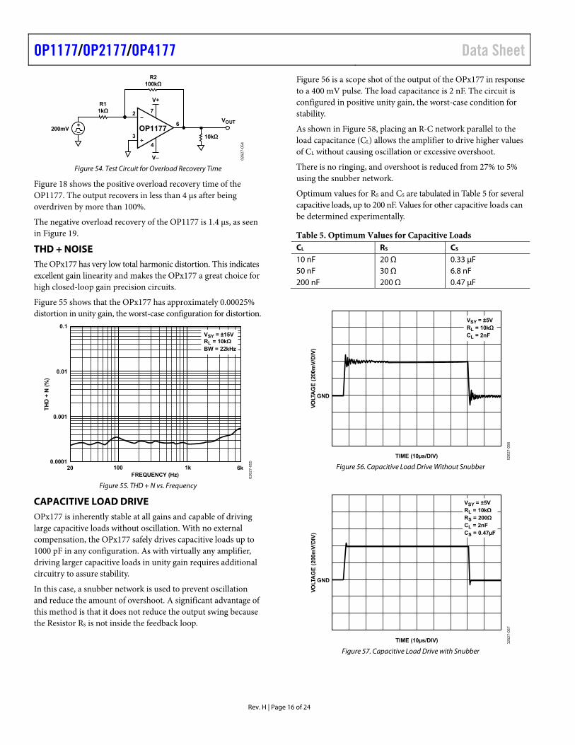
CAPACITIVE LOAD DRIVE OPx177 is inherently stable at all gains and capable of driving large capacitive loads without oscillation. With no external compensation, the OPx177 safely drives capacitive loads up to 1000 pF in any configuration. As with virtually any amplifier, driving larger capacitive loads in unity gain requires additional circuitry to assure stability.
In this case, a snubber network is used to prevent oscillation and reduce the amount of overshoot. A significant advantage of this method is that it does not reduce the output swing because the Resistor RS is not inside the feedback loop.
Figure 56 is a scope shot of the output of the OPx177 in response to a 400 mV pulse. The load capacitance is 2 nF. The circuit is configured in positive unity gain, the worst-case condition for stability.
As shown in Figure 58, placing an R-C network parallel to the load capacitance (CL) allows the amplifier to drive higher values of CL without causing oscillation or excessive overshoot.
There is no ringing, and overshoot is reduced from 27% to 5% using the snubber network.
Optimum values for RS and CS are tabulated in Table 5 for several capacitive loads, up to 200 nF. Values for other capacitive loads can be determined experimentally.
Table 5. Optimum Values for Capacitive Loads CL RS CS 10 nF 20 Ω 0.33 μF 50 nF 30 Ω 6.8 nF 200 nF 200 Ω 0.47 μF
0GND
VO
LTA
GE
(20
0mV
/DIV
)
TIME (10µs/DIV)
VSY = ±5VRL = 10kΩCL = 2nF
0262
7-05
6
Figure 56. Capacitive Load Drive Without Snubber
GND
VO
LTA
GE
(20
0mV
/DIV
)
TIME (10µs/DIV)
VSY = ±5VRL = 10kΩRS = 200ΩCL = 2nFCS = 0.47µF
0262
7-05
7
Figure 57. Capacitive Load Drive with Snubber
Data Sheet OP1177/OP2177/OP4177
Rev. H | Page 17 of 24
OP11776
72
3
4
V+
V–
VOUT
RS+–
400mV
CS
CL
0262
7-05
8
Figure 58. Snubber Network Configuration
Caution: The snubber technique cannot recover the loss of bandwidth induced by large capacitive loads.
STRAY INPUT CAPACITANCE COMPENSATION The effective input capacitance in an operational amplifier circuit (Ct) consists of three components. These are the internal differential capacitance between the input terminals, the internal common-mode capacitance of each input to ground, and the external capacitance including parasitic capacitance. In the circuit in Figure 59, the closed-loop gain increases as the signal frequency increases.
The transfer function of the circuit is
R1sCR1R2
t 1 1
indicating a zero at
tt CR2R1R2R1CR1R2s
/ 21
Depending on the value of R1 and R2, the cutoff frequency of the closed-loop gain can be well below the crossover frequency. In this case, the phase margin (ΦM) can be severely degraded, resulting in excessive ringing or even oscillation.
A simple way to overcome this problem is to insert a capacitor in the feedback path, as shown in Figure 60.
The resulting pole can be positioned to adjust the phase margin.
Setting Cf = (R1/R2) Ct achieves a phase margin of 90°. R2R1
V1
+
–OP1177
2
3
VOUTCt
0262
7-05
9
6
7
4
V+
V– Figure 59. Stray Input Capacitance
R2R1
V1
+
–OP1177
2
3
VOUTCt
Cf
0262
7-06
0
6
7
4
V+
V– Figure 60. Compensation Using Feedback Capacitor
REDUCING ELECTROMAGNETIC INTERFERENCE A number of methods can be utilized to reduce the effects of EMI on amplifier circuits.
In one method, stray signals on either input are coupled to the opposite input of the amplifier. The result is that the signal is rejected according to the CMRR of the amplifier.
This is usually achieved by inserting a capacitor between the inputs of the amplifier, as shown in Figure 61. However, this method can also cause instability, depending on the value of capacitance.
R2R1
V1
+
–OP1177
2
3
VOUTC
0262
7-06
1
6
7
4
V+
V– Figure 61. EMI Reduction
Placing a resistor in series with the capacitor (see Figure 62) increases the dc loop gain and reduces the output error. Positioning the breakpoint (introduced by R-C) below the secondary pole of the operational amplifier improves the phase margin and, therefore, stability.
R can be chosen independently of C for a specific phase margin according to the formula
R1R2
jfaR2R
2
1
where: a is the open-loop gain of the amplifier. f2 is the frequency at which the phase of a = ΦM − 180°.
OP1177
2
3
R
C
R1
R2
VOUTV1
+
–
0262
7-06
2
6
7
4
V+
V– Figure 62. Compensation Using Input R-C Network
OP1177/OP2177/OP4177 Data Sheet
Rev. H | Page 18 of 24
PROPER BOARD LAYOUT The OPx177 is a high precision device. To ensure optimum performance at the PCB level, care must be taken in the design of the board layout.
To avoid leakage currents, the surface of the board should be kept clean and free of moisture. Coating the surface creates a barrier to moisture accumulation and helps reduce parasitic resistance on the board.
Keeping supply traces short and properly bypassing the power supplies minimizes power supply disturbances due to output current variation, such as when driving an ac signal into a heavy load. Bypass capacitors should be connected as closely as possible to the device supply pins. Stray capacitances are a concern at the outputs and the inputs of the amplifier. It is recommended that signal traces be kept at least 5 mm from supply lines to minimize coupling.
A variation in temperature across the PCB can cause a mismatch in the Seebeck voltages at solder joints and other points where dissi-milar metals are in contact, resulting in thermal voltage errors. To minimize these thermocouple effects, orient resistors so heat sources warm both ends equally. Input signal paths should contain matching numbers and types of components, where possible to match the number and type of thermocouple junctions. For example, dummy components such as zero value resistors can be used to match real resistors in the opposite input path. Matching components should be located in close proximity and should be oriented in the same manner. Ensure leads are of equal length so that thermal conduction is in equilibrium. Keep heat sources on the PCB as far away from amplifier input circuitry as is practical.
The use of a ground plane is highly recommended. A ground plane reduces EMI noise and also helps to maintain a constant temperature across the circuit board.
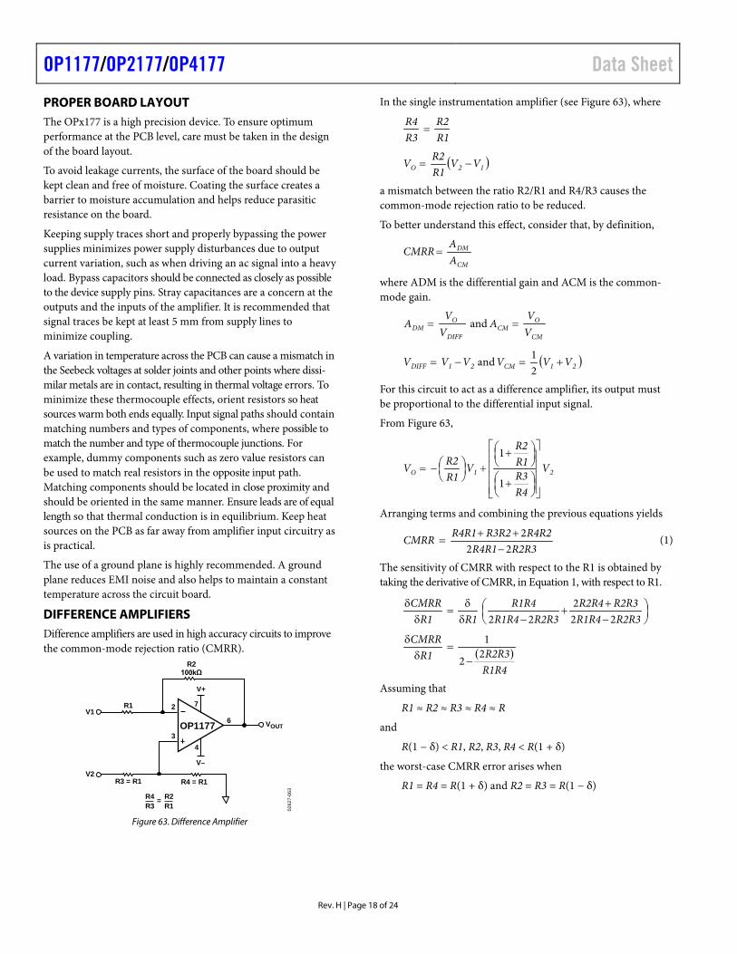
DIFFERENCE AMPLIFIERS Difference amplifiers are used in high accuracy circuits to improve the common-mode rejection ratio (CMRR).
R1V1
V2R3 = R1 R4 = R1
OP1177
2
3
=R4R3
R2R1
R2100kΩ
VOUT
0262
7-06
3
6
7
4
V+
V–
Figure 63. Difference Amplifier
In the single instrumentation amplifier (see Figure 63), where
R1R2
R3R4 =
( )12O VVR1R2V −=
a mismatch between the ratio R2/R1 and R4/R3 causes the common-mode rejection ratio to be reduced.
To better understand this effect, consider that, by definition,
CM
DM
AA
CMRR =
where ADM is the differential gain and ACM is the common-mode gain.
CM
OCM
DIFF
ODM V
VA
VV
A and ==
( )21CM21DIFF VVVVVV +=−= 21 and
For this circuit to act as a difference amplifier, its output must be proportional to the differential input signal.
From Figure 63,
21O V
R4R3R1R2
VR1R2V
1
1
+
+
+
−=
Arranging terms and combining the previous equations yields
R2R3R4R1R4R2R3R2R4R1CMRR
222
−++
= (1)
The sensitivity of CMRR with respect to the R1 is obtained by taking the derivative of CMRR, in Equation 1, with respect to R1.
−+
+−δ
δ=
δδ
R2R3R1R4R2R3R2R4
R2R3R1R4R1R4
R1R1CMRR
222
22
( )R1R4R2R3R1
CMRR22
1 −
=δ
δ
Assuming that
R1 ≈ R2 ≈ R3 ≈ R4 ≈ R
and
R(1 − δ) < R1, R2, R3, R4 < R(1 + δ)
the worst-case CMRR error arises when
R1 = R4 = R(1 + δ) and R2 = R3 = R(1 − δ)
Data Sheet OP1177/OP2177/OP4177
Rev. H | Page 19 of 24
Plugging these values into Equation 1 yields
δ≅
21 MINCMRR
where δ is the tolerance of the resistors.
Lower tolerance value resistors result in higher common-mode rejection (up to the CMRR of the operational amplifier).
Using 5% tolerance resistors, the highest CMRR that can be guaranteed is 20 dB. Alternatively, using 0.1% tolerance resistors results in a common-mode rejection ratio of at least 54 dB (assuming that the operational amplifier CMRR × 54 dB).
With the CMRR of OPx177 at 120 dB minimum, the resistor match is the limiting factor in most circuits. A trimming resistor can be used to further improve resistor matching and CMRR of the difference amplifier circuit.
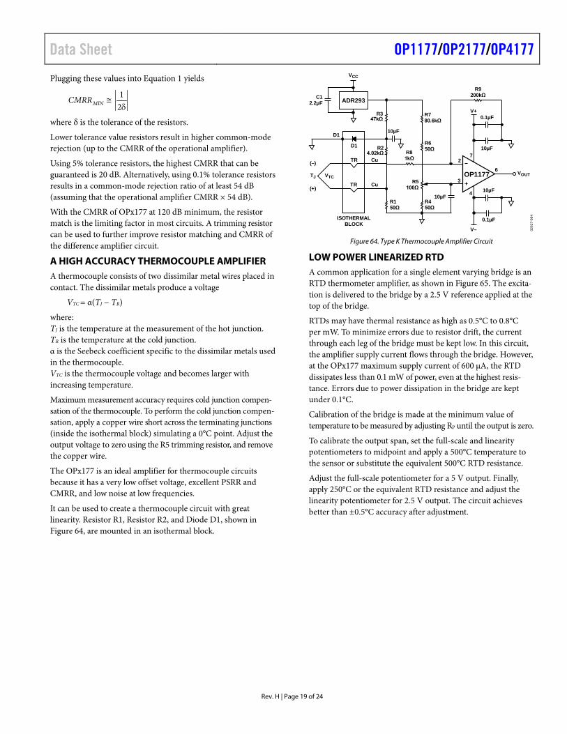
A HIGH ACCURACY THERMOCOUPLE AMPLIFIER A thermocouple consists of two dissimilar metal wires placed in contact. The dissimilar metals produce a voltage
VTC = α(TJ − TR)
where: TJ is the temperature at the measurement of the hot junction. TR is the temperature at the cold junction. α is the Seebeck coefficient specific to the dissimilar metals used in the thermocouple. VTC is the thermocouple voltage and becomes larger with increasing temperature.
Maximum measurement accuracy requires cold junction compen-sation of the thermocouple. To perform the cold junction compen-sation, apply a copper wire short across the terminating junctions (inside the isothermal block) simulating a 0°C point. Adjust the output voltage to zero using the R5 trimming resistor, and remove the copper wire.
The OPx177 is an ideal amplifier for thermocouple circuits because it has a very low offset voltage, excellent PSRR and CMRR, and low noise at low frequencies.
It can be used to create a thermocouple circuit with great linearity. Resistor R1, Resistor R2, and Diode D1, shown in Figure 64, are mounted in an isothermal block.
V+
7
4Cu
Cu
TR
TR
D1
D1
ADR293
VCC
C12.2µF
R347kΩ
10µF
R24.02kΩ R8
1kΩ
R780.6kΩ
R650Ω
R9200kΩ
0.1µF
10µF
0.1µF
10µF
V–
10µFR450Ω
R5100Ω
R150Ω
ISOTHERMALBLOCK
VTCTJ
(–)
(+)
6
2
3OP1177 VOUT
0262
7-06
4
Figure 64. Type K Thermocouple Amplifier Circuit
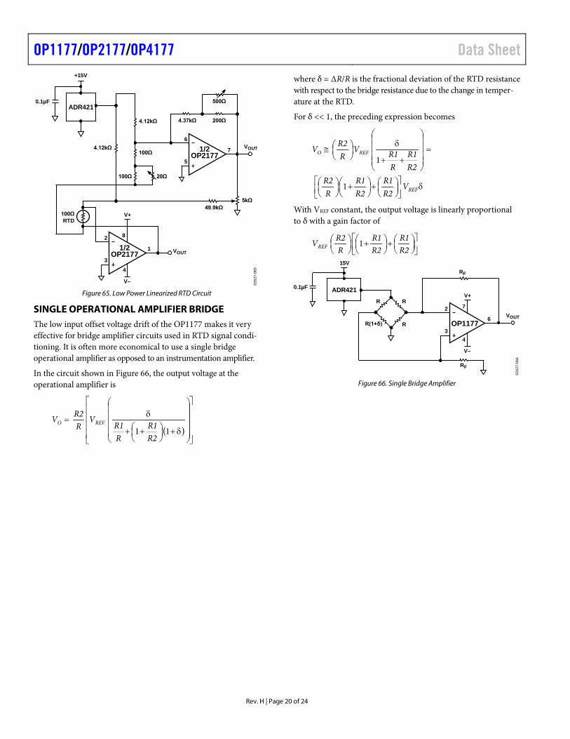
LOW POWER LINEARIZED RTD A common application for a single element varying bridge is an RTD thermometer amplifier, as shown in Figure 65. The excita-tion is delivered to the bridge by a 2.5 V reference applied at the top of the bridge.
RTDs may have thermal resistance as high as 0.5°C to 0.8°C per mW. To minimize errors due to resistor drift, the current through each leg of the bridge must be kept low. In this circuit, the amplifier supply current flows through the bridge. However, at the OPx177 maximum supply current of 600 µA, the RTD dissipates less than 0.1 mW of power, even at the highest resis-tance. Errors due to power dissipation in the bridge are kept under 0.1°C.
Calibration of the bridge is made at the minimum value of temperature to be measured by adjusting RP until the output is zero.
To calibrate the output span, set the full-scale and linearity potentiometers to midpoint and apply a 500°C temperature to the sensor or substitute the equivalent 500°C RTD resistance.
Adjust the full-scale potentiometer for a 5 V output. Finally, apply 250°C or the equivalent RTD resistance and adjust the linearity potentiometer for 2.5 V output. The circuit achieves better than ±0.5°C accuracy after adjustment.
OP1177/OP2177/OP4177 Data Sheet
Rev. H | Page 20 of 24
0262
7-06
5
200Ω
500Ω
4.37kΩ
100Ω
100Ω 20Ω
4.12kΩ
4.12kΩ
5kΩ49.9kΩ
ADR421
+15V
0.1µF
V+100ΩRTD
1/2OP2177
7
6
5
1/2OP2177
1
82
34
V–
VOUT
VOUT
Figure 65. Low Power Linearized RTD Circuit
SINGLE OPERATIONAL AMPLIFIER BRIDGE The low input offset voltage drift of the OP1177 makes it very effective for bridge amplifier circuits used in RTD signal condi-tioning. It is often more economical to use a single bridge operational amplifier as opposed to an instrumentation amplifier.
In the circuit shown in Figure 66, the output voltage at the operational amplifier is
( )
δ+
++
δ=
1 1
R2R1
RR1
VR
R2V REFO
where δ = ∆R/R is the fractional deviation of the RTD resistance with respect to the bridge resistance due to the change in temper-ature at the RTD.
For δ << 1, the preceding expression becomes
δ
+
+
=
++
δ
≅
REF
REFO
VR2R1
R2R1
RR2
R2R1
RR1V
RR2
V
1
1
With VREF constant, the output voltage is linearly proportional to δ with a gain factor of
+
+
R2R1
R2R1
RR2VREF 1
0262
7-06
6
R
R
R
R(1+δ)
ADR421
15V
0.1µF
OP11776
7
4
2
3
V+
V–
RF
RF
VOUT
Figure 66. Single Bridge Amplifier
Data Sheet OP1177/OP2177/OP4177
Rev. H | Page 21 of 24
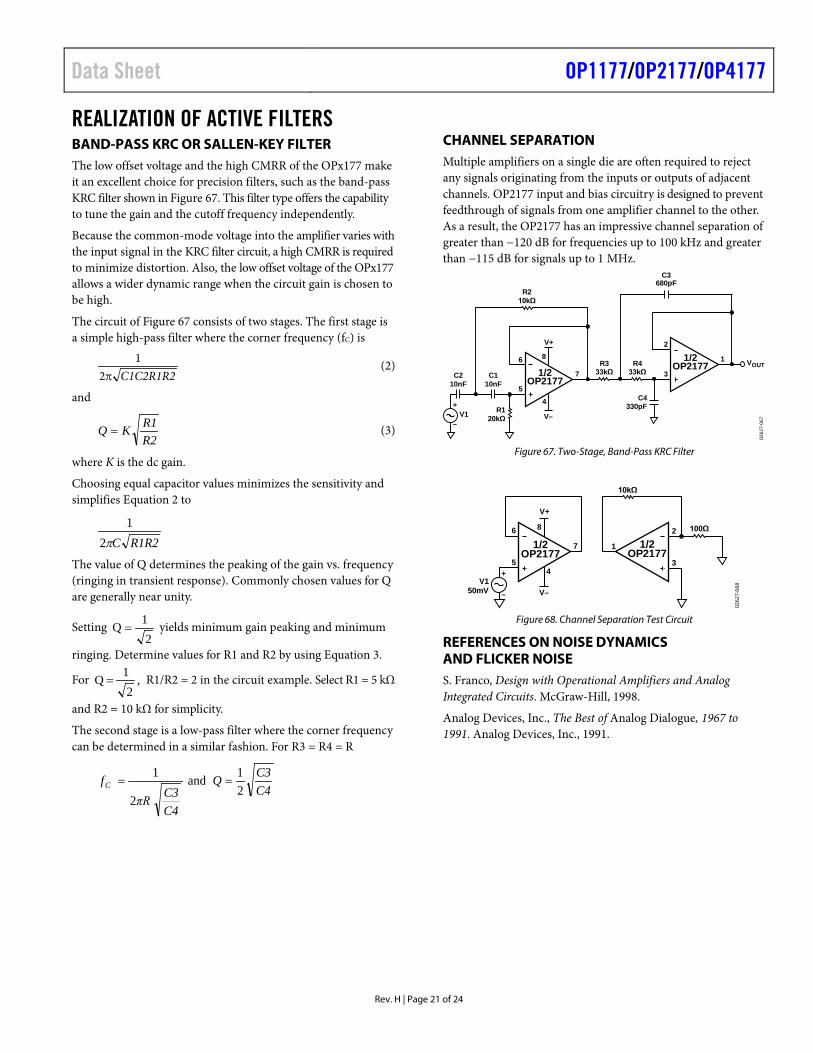
REALIZATION OF ACTIVE FILTERS BAND-PASS KRC OR SALLEN-KEY FILTER The low offset voltage and the high CMRR of the OPx177 make it an excellent choice for precision filters, such as the band-pass KRC filter shown in Figure 67. This filter type offers the capability to tune the gain and the cutoff frequency independently.
Because the common-mode voltage into the amplifier varies with the input signal in the KRC filter circuit, a high CMRR is required to minimize distortion. Also, the low offset voltage of the OPx177 allows a wider dynamic range when the circuit gain is chosen to be high.
The circuit of Figure 67 consists of two stages. The first stage is a simple high-pass filter where the corner frequency (fC) is
C1C2R1R2π21 (2)
and
R2R1KQ = (3)
where K is the dc gain.
Choosing equal capacitor values minimizes the sensitivity and simplifies Equation 2 to
R1R2Cπ21
The value of Q determines the peaking of the gain vs. frequency (ringing in transient response). Commonly chosen values for Q are generally near unity.
Setting 2
1Q = yields minimum gain peaking and minimum
ringing. Determine values for R1 and R2 by using Equation 3.
For ,2
1Q = R1/R2 = 2 in the circuit example. Select R1 = 5 kΩ
and R2 = 10 kΩ for simplicity.
The second stage is a low-pass filter where the corner frequency can be determined in a similar fashion. For R3 = R4 = R
C4C3Q
C4C3πR
f C 21and
2
1==
CHANNEL SEPARATION Multiple amplifiers on a single die are often required to reject any signals originating from the inputs or outputs of adjacent channels. OP2177 input and bias circuitry is designed to prevent feedthrough of signals from one amplifier channel to the other. As a result, the OP2177 has an impressive channel separation of greater than −120 dB for frequencies up to 100 kHz and greater than −115 dB for signals up to 1 MHz.
0262
7-06
7
C3680pF
1/2OP2177
7
86
54
V+
V–
1/2OP2177
1
2
3
R210kΩ
V1+
–
R120kΩ
C210nF
C110nF
R333kΩ
R433kΩ
C4330pF
VOUT
Figure 67. Two-Stage, Band-Pass KRC Filter
1
2
3
1/2OP2177
100Ω
10kΩ
1/2OP2177
7
86
54
V+
V–
+
–
0262
7-06
8V150mV
Figure 68. Channel Separation Test Circuit
REFERENCES ON NOISE DYNAMICS AND FLICKER NOISE S. Franco, Design with Operational Amplifiers and Analog Integrated Circuits. McGraw-Hill, 1998.
Analog Devices, Inc., The Best of Analog Dialogue, 1967 to 1991. Analog Devices, Inc., 1991.

OP1177/OP2177/OP4177 Data Sheet
Rev. H | Page 22 of 24
OUTLINE DIMENSIONS
CONTROLLING DIMENSIONS ARE IN MILLIMETERS; INCH DIMENSIONS(IN PARENTHESES) ARE ROUNDED-OFF MILLIMETER EQUIVALENTS FORREFERENCE ONLY AND ARE NOT APPROPRIATE FOR USE IN DESIGN.
COMPLIANT TO JEDEC STANDARDS MS-012-AA
0124
07-A
0.25 (0.0098)0.17 (0.0067)
1.27 (0.0500)0.40 (0.0157)
0.50 (0.0196)0.25 (0.0099) 45°
8°0°
1.75 (0.0688)1.35 (0.0532)
SEATINGPLANE
0.25 (0.0098)0.10 (0.0040)
41
8 5
5.00 (0.1968)4.80 (0.1890)
4.00 (0.1574)3.80 (0.1497)
1.27 (0.0500)BSC
6.20 (0.2441)5.80 (0.2284)
0.51 (0.0201)0.31 (0.0122)
COPLANARITY0.10
Figure 69. 8-Lead Standard Small Outline Package [SOIC_N]
Narrow Body (R-8)
Dimensions shown in millimeters and (inches)
CONTROLLING DIMENSIONS ARE IN MILLIMETERS; INCH DIMENSIONS(IN PARENTHESES) ARE ROUNDED-OFF MILLIMETER EQUIVALENTS FORREFERENCE ONLY AND ARE NOT APPROPRIATE FOR USE IN DESIGN.
COMPLIANT TO JEDEC STANDARDS MS-012-AB
0606
06-A
14 8
71
6.20 (0.2441)5.80 (0.2283)
4.00 (0.1575)3.80 (0.1496)
8.75 (0.3445)8.55 (0.3366)
1.27 (0.0500)BSC
SEATINGPLANE
0.25 (0.0098)0.10 (0.0039)
0.51 (0.0201)0.31 (0.0122)
1.75 (0.0689)1.35 (0.0531)
0.50 (0.0197)0.25 (0.0098)
1.27 (0.0500)0.40 (0.0157)
0.25 (0.0098)0.17 (0.0067)
COPLANARITY0.10
8°0°
45°
Figure 70. 14-Lead Standard Small Outline Package [SOIC_N]
Narrow Body (R-14)
Dimensions shown in millimeters and (inches)
Data Sheet OP1177/OP2177/OP4177
Rev. H | Page 23 of 24
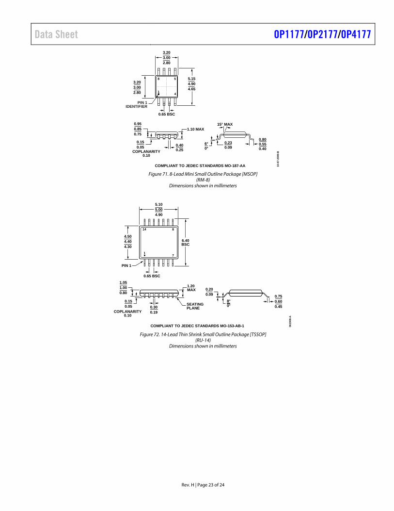
COMPLIANT TO JEDEC STANDARDS MO-187-AA
6°0°
0.800.550.40
4
8
1
5
0.65 BSC
0.400.25
1.10 MAX
3.203.002.80
COPLANARITY0.10
0.230.09
3.203.002.80
5.154.904.65
PIN 1IDENTIFIER
15° MAX0.950.850.75
0.150.05
10-0
7-20
09-B
Figure 71. 8-Lead Mini Small Outline Package [MSOP]
(RM-8) Dimensions shown in millimeters
COMPLIANT TO JEDEC STANDARDS MO-153-AB-1 0619
08-A
8°0°
4.504.404.30
14 8
71
6.40BSC
PIN 1
5.105.004.90
0.65 BSC
0.150.05 0.30
0.19
1.20MAX
1.051.000.80
0.200.09 0.75
0.600.45
COPLANARITY0.10
SEATINGPLANE
Figure 72. 14-Lead Thin Shrink Small Outline Package [TSSOP]
(RU-14) Dimensions shown in millimeters
OP1177/OP2177/OP4177 Data Sheet
Rev. H | Page 24 of 24
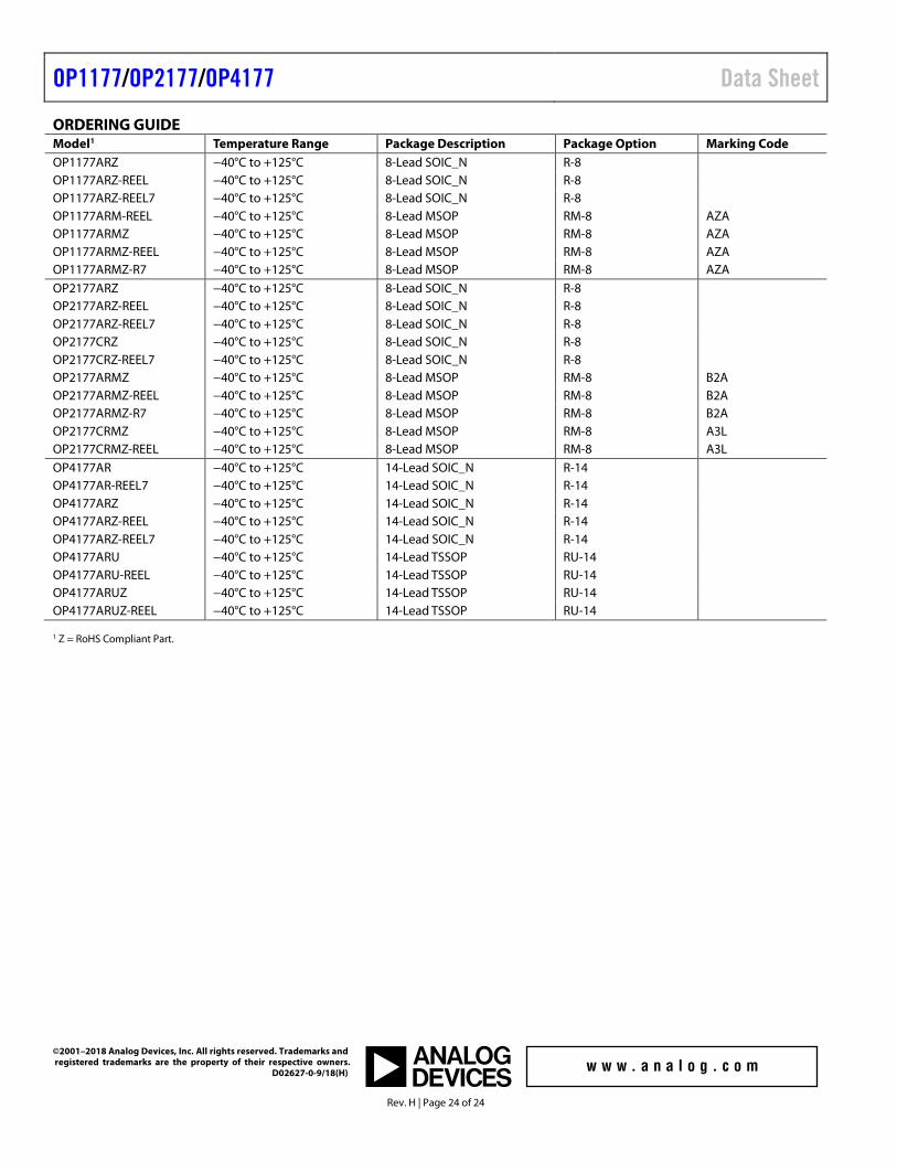
ORDERING GUIDE Model1 Temperature Range Package Description Package Option Marking Code OP1177ARZ −40°C to +125°C 8-Lead SOIC_N R-8 OP1177ARZ-REEL −40°C to +125°C 8-Lead SOIC_N R-8 OP1177ARZ-REEL7 −40°C to +125°C 8-Lead SOIC_N R-8 OP1177ARM-REEL −40°C to +125°C 8-Lead MSOP RM-8 AZA OP1177ARMZ −40°C to +125°C 8-Lead MSOP RM-8 AZA OP1177ARMZ-REEL −40°C to +125°C 8-Lead MSOP RM-8 AZA OP1177ARMZ-R7 −40°C to +125°C 8-Lead MSOP RM-8 AZA OP2177ARZ −40°C to +125°C 8-Lead SOIC_N R-8 OP2177ARZ-REEL −40°C to +125°C 8-Lead SOIC_N R-8 OP2177ARZ-REEL7 −40°C to +125°C 8-Lead SOIC_N R-8 OP2177CRZ −40°C to +125°C 8-Lead SOIC_N R-8 OP2177CRZ-REEL7 −40°C to +125°C 8-Lead SOIC_N R-8 OP2177ARMZ −40°C to +125°C 8-Lead MSOP RM-8 B2A OP2177ARMZ-REEL −40°C to +125°C 8-Lead MSOP RM-8 B2A OP2177ARMZ-R7 −40°C to +125°C 8-Lead MSOP RM-8 B2A OP2177CRMZ −40°C to +125°C 8-Lead MSOP RM-8 A3L OP2177CRMZ-REEL −40°C to +125°C 8-Lead MSOP RM-8 A3L OP4177AR −40°C to +125°C 14-Lead SOIC_N R-14 OP4177AR-REEL7 −40°C to +125°C 14-Lead SOIC_N R-14 OP4177ARZ −40°C to +125°C 14-Lead SOIC_N R-14 OP4177ARZ-REEL −40°C to +125°C 14-Lead SOIC_N R-14 OP4177ARZ-REEL7 −40°C to +125°C 14-Lead SOIC_N R-14 OP4177ARU −40°C to +125°C 14-Lead TSSOP RU-14 OP4177ARU-REEL −40°C to +125°C 14-Lead TSSOP RU-14 OP4177ARUZ −40°C to +125°C 14-Lead TSSOP RU-14 OP4177ARUZ-REEL −40°C to +125°C 14-Lead TSSOP RU-14 1 Z = RoHS Compliant Part.
©2001–2018 Analog Devices, Inc. All rights reserved. Trademarks and registered trademarks are the property of their respective owners. D02627-0-9/18(H)