Embed Size (px)
Citation preview

System Power Management and Portable Power
2.0
1. Point-of-Load Power2. System Power Management and Portable Power3. Power for Mixed Analog/Digital Systems 4. Hardware Design Techniques
Practical Power Solutions
Copyright © 2009 By Analog Devices, Inc.All rights reserved. This book, or parts thereof, must not be reproduced in any form without permission of the copyright owner.
SECTION 2SYSTEM POWER MANAGEMENT AND PORTABLE POWER
Designing a Typical System Power Chain..........................................................................2.1Microprocessor Supervisory Functions.........................................................................2.13Power Supply Monitoring and Sequencing......................................................................2.20Hot Swap Controllers..........................................................................................................2.32Temperature Monitoring...................................................................................................2.42Digital Isolation and Isolated Power...............................................................................2.48Digital Power Applications.................................................................................................2.58Powering Portable Systems..............................................................................................2.63Technical References.......................................................................................................2.76
System Power Management and Portable Power
2.1
Designing a Typical SystemPower Chain
System Power Management and Portable Power
2.2
A Typical System Using AC Power
MEMORY2.5V @ 1A
ADSP-BF535 DSP CORE
1.5V @ 0.5A
CPU CORE1.2V @ 5A
CPU I/O2.5V @ 0.5A
ADSP-BF535 DSP I/O
3.3V @ 0.1A
AUDIO POWER AMP12V @ 1A
HARD DISK DRIVE5V @ 2A
???
100V to 250VAC
PEAK VALUES ASSUMED FOR CURRENTS AT NOMINAL VOLTAGES
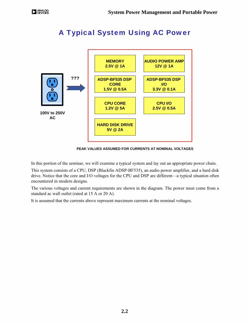
In this portion of the seminar, we will examine a typical system and lay out an appropriate power chain.This system consists of a CPU, DSP (Blackfin ADSP-BF535), an audio power amplifier, and a hard disk drive. Notice that the core and I/O voltages for the CPU and DSP are different—a typical situation often encountered in modern designs.The various voltages and current requirements are shown in the diagram. The power must come from a standard ac wall outlet (rated at 15 A or 20 A). It is assumed that the currents above represent maximum currents at the nominal voltages.

System Power Management and Portable Power
2.3
End Power Requirements for System
32.83Total Power
0.330.103.30ADSP-BF535 DSP I/O
0.750.501.50ADSP-BF535 DSP Core
10.002.005.00Hard Disk Drive
2.501.002.50Memory
1.250.502.50CPU I/O
6.005.001.20CPU Core
12.001.0012.00Audio Power Amp
Power (W)Current (A)Voltage (V)Function
PEAK VALUES ASSUMED FOR CURRENTS AT NOMINAL VOLTAGES
This figure breaks out the various voltages and currents required to power the system. The total power consumed is 32.83 W.

System Power Management and Portable Power
2.4
General Guidelines for Power Trains
Start with higher voltages and regulate down (buck), not up (boost)Do not make more voltages than you actually need
Exception: For a low noise power rail, you may need to pre-regulate the input of an LDO with a buck (or maybe a boost) converter to keep power dissipation in the LDO low
Do not run the power through more conversions than you need:
91% EFFICIENTDC-to-DC CONVERTER
94% EFFICIENTDC-to-DC CONVERTER
12V 5V 1.2V @ 5A
OVERALL EFFICIENCY = 0.91 × 0.94 × 100% = 85.5%
86% EFFICIENTDC-to-DC CONVERTER
12V 1.2V @ 5A
OVERALL EFFICIENCY = 86%
Before starting the design, it is useful to examine several useful guidelines relating to fixed (non-portable) power system design.As previously discussed, it is wise to distribute higher voltages and then regulate down from them at the points-of-load using buck regulators or LDOs. It is generally unwise to use boost converters in fixed power applications. These are much more suitable for battery-operated portable systems. However, if the current is low enough, a boost converter can be useful in certain applications. You should also try and design the system with as few voltages as possible; i.e. do not generate intermediate bus voltages that are not used in the system. There is one important exception to this rule where it is desirable to use an LDO to generate a low noise supply voltage, perhaps to power a mixed-signal device such as an ADC, PLL, or other noise-sensitive analog circuit. In this case it may be wise to use a buck converter (in some cases a boost converter) as a pre-regulator for the LDO. The output of the buck or boost converter is made slightly higher than the LDO output voltage plus the LDO dropout voltage. This minimizes power dissipation in the LDO.Finally, try and minimize the number of power conversions in any given power path. Remember that the overall efficiency of two converters in series is equal to the product of the individual efficiencies. A 91% efficient converter in series with a 94% efficient converter yields a total efficiency of 85.5%. The example above shows that the 12 V to 1.2 V buck converter is only 86% efficient, primarily because of the high VIN/VOUT ratio. Even though the individual 12 V to 5 V and 5 V to 1.2 V converters are more efficient (91% and 94%, respectively), their combined efficiency of 85.5% is no better than using the single converter.

System Power Management and Portable Power
2.5
Choice of AC Power Adapter
5V, 9V, 12V, 18V, 24V ????
This is the largest voltage that we need in the systemWe don't have to use a separate regulator for the 12V audio ampWe can regulate down from here to get the other voltages
The first step in the power design is to select the ac adapter output voltage. These adapters are available with a number of different dc voltage outputs.We will select a 12 V adapter because 12 V can be used directly by the power amplifier. This way the power amplifier does not need its own regulator. Here we are assuming that after proper filtering, the 12xV supply is "quiet" enough to power the audio amplifier. The 12 V output can be regulated down to get the other voltages required in the system.

System Power Management and Portable Power
2.6
After Choosing a 12V Power Bus, What is the Next Step?
MEMORY2.5V @ 1A
ADSP-BF535 DSPCORE
1.5V @ 0.5A
CPU CORE1.2V @ 5A
CPU I/O2.5V @ 0.5A
ADSP-BF535 DSP I/O
3.3V @ 0.1A
AUDIO POWER AMP12V @ 1A
HARD DISK DRIVE5V @ 2A
100V to 250VAC
12V
HIGH CURRENT DEVICES
Now that 12 V has been chosen as the primary dc bus, what is the next step in the design?A good place to start is to examine the requirements for the voltages which require the largest current: the 1.2 V CPU core voltage (5 A) and the 5 V hard disk drive (2 A).

System Power Management and Portable Power
2.7
Powering the High Current Devices from a Dual Synchronous Buck Controller
CPU CORE1.2V @ 5AADP1829 DUAL
SYNC. BUCKCONTROLLER
AUDIO POWER AMP12V @ 1A
HARD DISK DRIVE
5V @ 2A
12V
1.2V
5V
USE INTERMEDIATE BUSFOR THE REMAINDER OF THE SYSTEM
12V
FROMAC ADAPTER
Since there are two relatively high current rails, a dual synchronous buck controller such as the ADP1829 can be used to generate both the 5 V and 1.2 V rails from the 12 V input. The 5 V rail can then be used as an intermediate bus to generate the lower voltages required in the system. Although it would be possible to generate the 1.2 V CPU core voltage from the intermediate 5 V bus, this puts two high current regulators in series, and the overall efficiency will be no better than generating the 1.2 V directly from the 12 V rail.

System Power Management and Portable Power
2.8
Finishing the Design using the 5VIntermediate Bus and More POL Regulators
CPU CORE1.2V @ 5AADP1829 DUAL
SYNC. BUCKCONTROLLER
AUDIO POWER AMP12V @ 1A
HARD DISK DRIVE
5V @ 2A
12V
1.2V
5V
12V
FROMAC ADAPTER
ADP17061A LDO
ADP21072A SYNC.
BUCK REG.
ADP17061A LDO
ADSP-BF535 DSP CORE1.5V @ 0.5A
MEMORY2.5V @ 1A
CPU I/O2.5V @ 0.5A
ADSP-BF535DSP I/O
3.3V @ 0.1A
3.3V
2.5V
1.5V2A≈ 1A
≈ 3.1A
ADP1710 150mA LDO could be used here,but has no soft-start feature
Continuing with the design, we will use an LDO to generate the 3.3 V required for the DSP I/O because the current requirement is only 0.1 A. The ADP1710 150 mA low cost LDO comes in a 5-lead TSOT package and has a worst case θJA = 170°C/W (assuming no surrounding copper area). In the circuit the part dissipates 0.17 W, giving a 29°C rise from ambient-to-junction. Although this is more than adequate for operation at 85°C ambient, the ADP1710 does not have a soft-start feature which might be needed for sequencing. The ADP1706 handles 1 A and has a worst case θJA of 58°C/W in the 8-lead, exposed paddle SOIC; and a worst case θJA of 66°C/W in the 8-lead exposed paddle LFCSP. This part is rated for 1 A and has a soft-start feature.We will use the ADP2107 2 A synchronous buck regulator to generate the 2.5 V for the CPU I/O and the memory. The ADP1706 LDO is used to generate the 1.5 V core voltage for the DSP. In the circuit, the ADP1706 dissipates 0.5 W, so this yields an ambient to junction rise of 33°C using θJA = 66°C/W.In order to maintain parts commonality and to allow for soft-start capability, we will use the ADP1706 LDO in both applications.
System Power Management and Portable Power
2.9
Overall System Efficiency Calculations
CPU CORE1.2V @ 5AADP1829 DUAL
SYNC. BUCKCONTROLLER
AUDIO POWER AMP12V @ 1A
HARD DISK DRIVE
5V @ 2A
12V
1.2V
5V
12V
FROMAC ADAPTER
ADP1706LDO
ADP2107SYNC.
BUCK REG.
ADP1706LDO
ADSP-BF535 DSP CORE1.5V @ 0.5A
MEMORY2.5V @ 1A
CPU I/O2.5V @ 0.5A
ADSP-BF535DSP I/O
3.3V @ 0.1A
3.3V
2.5V
1.5V2A
60% EFFPLOSS = 0.5W
90% EFFPLOSS = 0.56W
90% EFF, EACHHALFPLOSS 1.2V = 0.67WPLOSS 5V = 1.78W
66% EFFPLOSS = 0.17W
12W
6W
10W
0.33W
1.25W
2.5W
0.75W
TOTAL INPUT POWER = 24.51WTOTAL LOSS = 3.68WTOTAL OUTPUT POWER = 20.83W
TOTAL EFF = POUT/PIN = 84.99%
1.11A
3.21A
Not included inefficiency calculations
2.05A3.05A
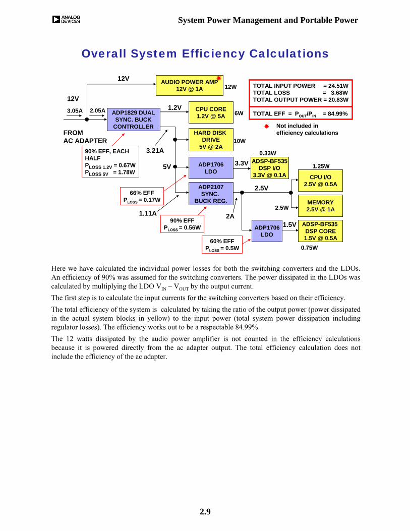
Here we have calculated the individual power losses for both the switching converters and the LDOs. An efficiency of 90% was assumed for the switching converters. The power dissipated in the LDOs was calculated by multiplying the LDO VIN – VOUT by the output current.The first step is to calculate the input currents for the switching converters based on their efficiency.The total efficiency of the system is calculated by taking the ratio of the output power (power dissipated in the actual system blocks in yellow) to the input power (total system power dissipation including regulator losses). The efficiency works out to be a respectable 84.99%.The 12 watts dissipated by the audio power amplifier is not counted in the efficiency calculations because it is powered directly from the ac adapter output. The total efficiency calculation does not include the efficiency of the ac adapter.

System Power Management and Portable Power
2.10
Efficiency Comparison: ADP2107 Synchronous Regulator vs. ADP1864 Asynchronous Controller
ADP2105/ADP2106/ADP2107: Synchronous Buck Regulator, Internal Switches
Optimized for output currents of 1A (ADP2105), 1.5A (ADP2106), and 2A (ADP2107).VIN = 2.7V to 5.5V, VOUT = 0.8V to VINSynchronous gives good efficiency for higher currents, low voltages1.2MHz Switching FrequencyFor output currents less than 0.6A, ADP2102 or ADP2108 regulators offer compact solutions at 3MHz switching frequencies
ADP1864: Asynchronous Buck Controller, External PMOS FET and Schottky diode
VIN = 3.15V to 14V, VOUT = 0.8V to VINGenerally used for outputs up to 5ADiode limits efficiency for high currents, low output voltages580kHz Switching Frequency
For output currents less than a few amps, a synchronous buck regulator is a good choice, such as the ADP2105 (1 A), ADP2106 (1.5 A), and ADP2107 (2 A). The switches are integrated, and the parts therefore require only a few external components for a complete design. The synchronous switch gives good efficiency, especially for higher currents and low output voltages. For currents of 600 mA or less, the ADP2102 and ADP2108 offer compact solutions because of their 3xMHz switching frequencies.On the other hand, an asynchronous buck regulator using external components, such as the ADP1864, can be configured to supply more output current with a higher parts count and larger size. The ADP1864 is useful for output currents up to about 5 A. In this exercise, we will let ADIsimPower create two designs. The first design uses the ADP2107 synchronous regulator, and the second design uses the ADP1864 asynchronous buck controller. The ADIsimPower designs allow comparisons between the efficiency, cost, and board space for the two approaches.
System Power Management and Portable Power
2.11
Design Solutions Using ADIsimPower
366mW88mW
10µF×2
2.7µH
10µF2.2µH
47µF×2
22µF+10µF
51.1kΩ
100kΩ
56pF
12.4kΩ
1nF 33mΩ
178kΩ
47pF
VIN = 5VVIN = 5V
VOUT1.2V
390mW
128mW
VIN = 5VVOUT = 1.2V @ 2APOUT = 2.4WPLOSS = 530mWEFF = 82%
COST ≈ $2.63AREA ≈ 74mm2
VIN = 5VVOUT = 1.2V @ 2APOUT = 2.4WPLOSS = 516mWEFF = 82%
COST ≈ $3.02AREA ≈ 333mm2
VOUT1.2V
ADP2107 DESIGN ADP1864 DESIGN
ADP2107
1nF
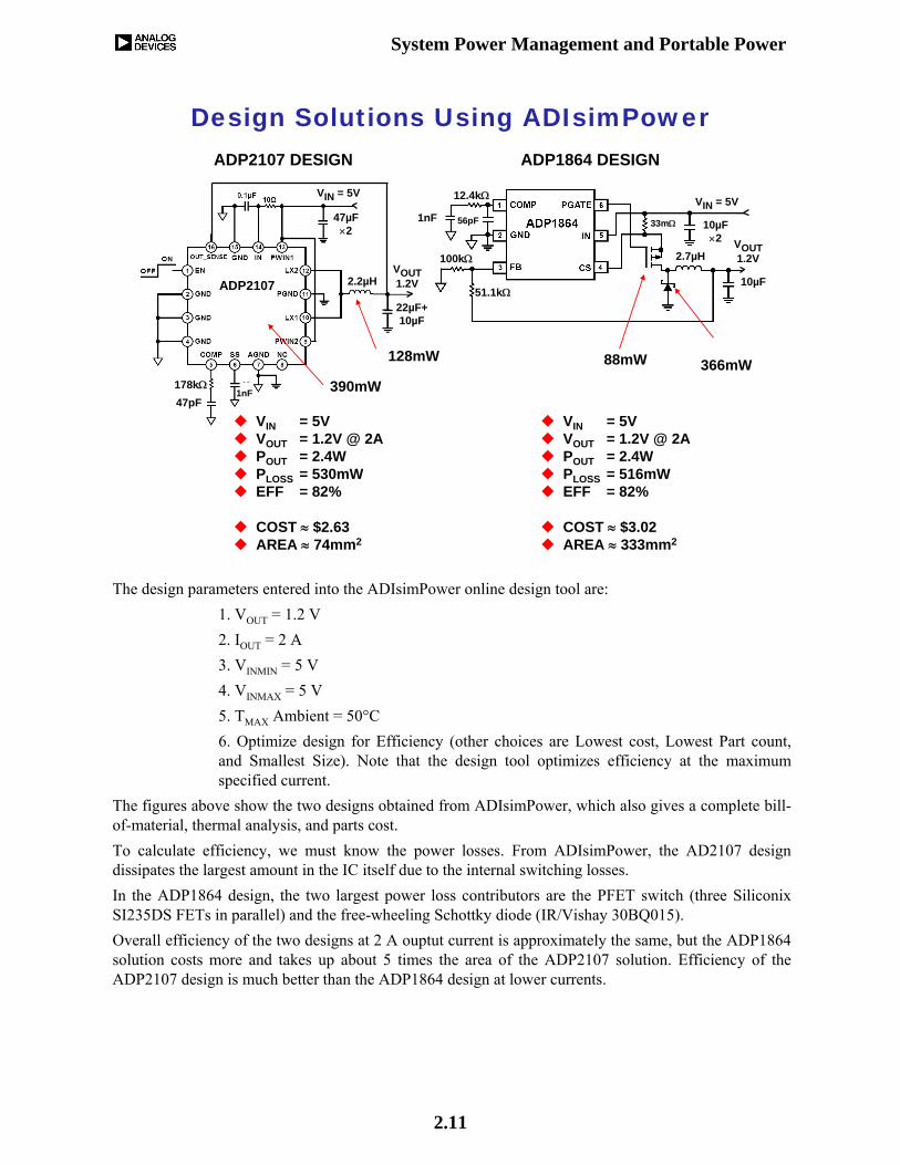
The design parameters entered into the ADIsimPower online design tool are:1. VOUT = 1.2 V2. IOUT = 2 A3. VINMIN = 5 V4. VINMAX = 5 V5. TMAX Ambient = 50°C6. Optimize design for Efficiency (other choices are Lowest cost, Lowest Part count, and Smallest Size). Note that the design tool optimizes efficiency at the maximum specified current.
The figures above show the two designs obtained from ADIsimPower, which also gives a complete bill-of-material, thermal analysis, and parts cost.To calculate efficiency, we must know the power losses. From ADIsimPower, the AD2107 design dissipates the largest amount in the IC itself due to the internal switching losses. In the ADP1864 design, the two largest power loss contributors are the PFET switch (three SiliconixSI235DS FETs in parallel) and the free-wheeling Schottky diode (IR/Vishay 30BQ015). Overall efficiency of the two designs at 2 A ouptut current is approximately the same, but the ADP1864 solution costs more and takes up about 5 times the area of the ADP2107 solution. Efficiency of the ADP2107 design is much better than the ADP1864 design at lower currents.

System Power Management and Portable Power
2.12
Efficiency of ADP1864 Asynchronous Buck Controller vs. ADP2107 PFM Synchronous Buck Regulator
VIN = 5V, VOUT = 1.2V
ADP2107
ADP1864
95%
90%
85%
80%
75%
70%
65%
0 0.2 0.4 0.6 0.8 1.0 1.2 1.4 1.6 1.8 2.0
EFFI
CIE
NC
Y
OUTPUT CURRENT (A)
This shows the efficiency of the two designs from output currents of 10 mA up to 2 A. The ADP2107 smoothly transitions from the PWM (pulse width modulation) mode to the variable frequency PFM (pulse frequency mode) mode of operation when the load current decreases below the pulse-skipping threshold current, switching only as necessary to maintain the output voltage within regulation. When the output voltage first dips below regulation, the ADP2107 enters the PFM mode for a few oscillator cycles to increase the output voltage back to regulation. During the wait time between bursts, both power switches are off, and the output capacitor supplies all the load current. Because the output voltage dips and recovers occasionally, the output voltage ripple in this mode is larger than the ripple in the PWM mode of operation.The output current at which the ADP2107 transitions from variable frequency PFM control to fixed frequency PWM control is called the pulse-skipping threshold. The pulse-skipping threshold has been optimized for excellent efficiency over all load currents. The efficiency of the ADP1864 design is not as good at low currents, and the cost, parts count, and area is greater.The obvious conclusion is that it is better to use a fully integrated PFM synchronous regulator where possible for currents of a few amps or less.

System Power Management and Portable Power
2.13
Microprocessor Supervisory Functions
www.analog.com/supervisory
System Power Management and Portable Power
2.14
Simple Reset and Power-On Reset GeneratorRESET
TRIP POINT OPTIONS
OUTPUTOPTIONS
PACKAGEOPTIONS
RESETTIMEOUTOPTIONS
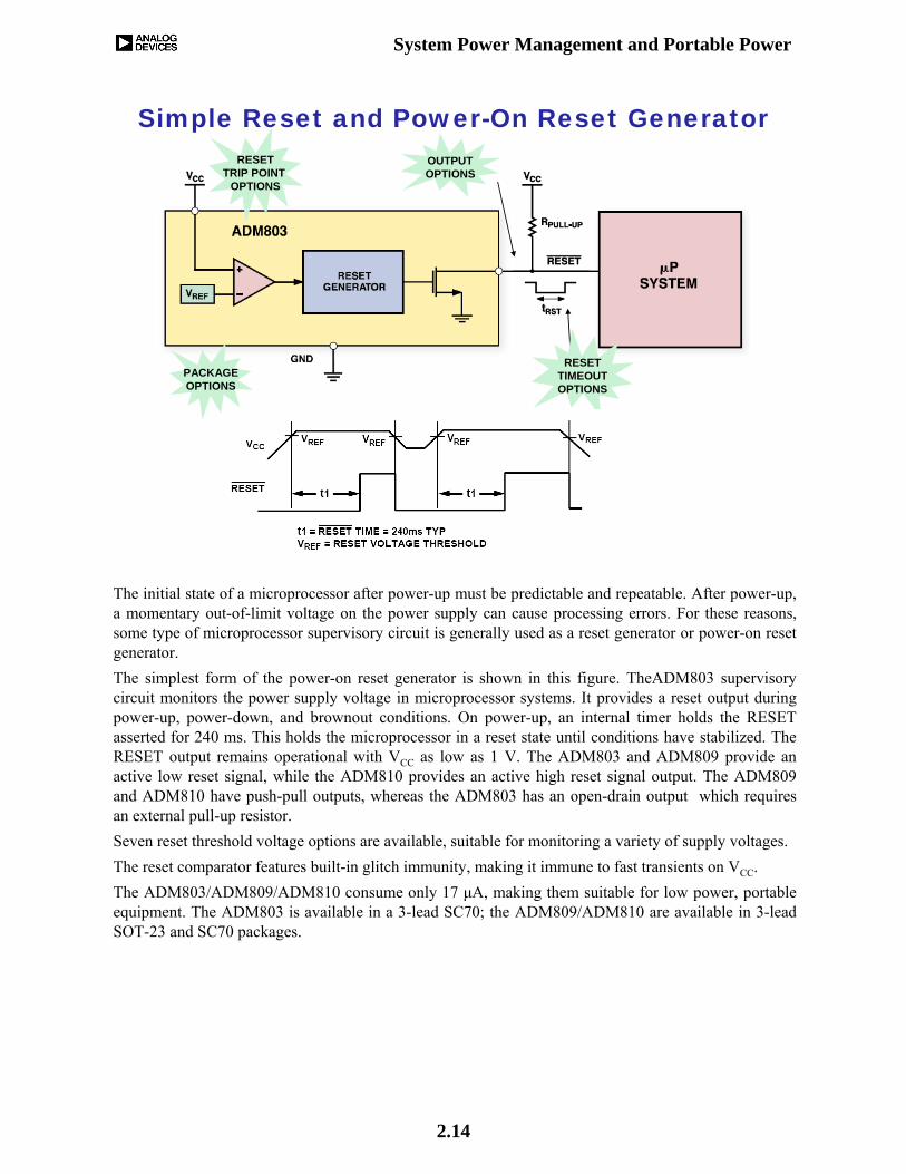
The initial state of a microprocessor after power-up must be predictable and repeatable. After power-up, a momentary out-of-limit voltage on the power supply can cause processing errors. For these reasons, some type of microprocessor supervisory circuit is generally used as a reset generator or power-on reset generator.The simplest form of the power-on reset generator is shown in this figure. TheADM803 supervisory circuit monitors the power supply voltage in microprocessor systems. It provides a reset output during power-up, power-down, and brownout conditions. On power-up, an internal timer holds the RESET asserted for 240 ms. This holds the microprocessor in a reset state until conditions have stabilized. The RESET output remains operational with VCC as low as 1 V. The ADM803 and ADM809 provide an active low reset signal, while the ADM810 provides an active high reset signal output. The ADM809 and ADM810 have push-pull outputs, whereas the ADM803 has an open-drain output which requires an external pull-up resistor.Seven reset threshold voltage options are available, suitable for monitoring a variety of supply voltages.The reset comparator features built-in glitch immunity, making it immune to fast transients on VCC.The ADM803/ADM809/ADM810 consume only 17 μA, making them suitable for low power, portable equipment. The ADM803 is available in a 3-lead SC70; the ADM809/ADM810 are available in 3-lead SOT-23 and SC70 packages.
System Power Management and Portable Power
2.15
ADM6710 Low Voltage Quad Supervisory Circuit
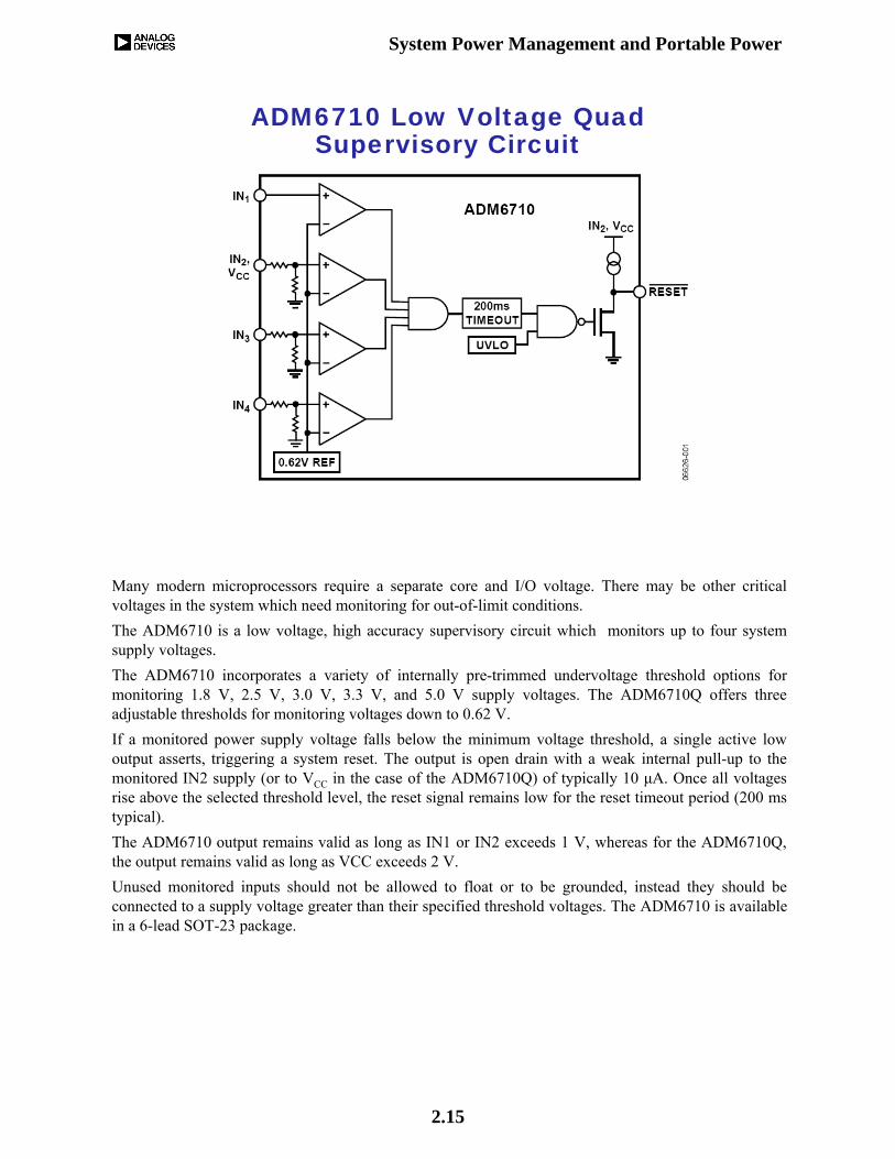
Many modern microprocessors require a separate core and I/O voltage. There may be other critical voltages in the system which need monitoring for out-of-limit conditions.The ADM6710 is a low voltage, high accuracy supervisory circuit which monitors up to four system supply voltages. The ADM6710 incorporates a variety of internally pre-trimmed undervoltage threshold options for monitoring 1.8 V, 2.5 V, 3.0 V, 3.3 V, and 5.0 V supply voltages. The ADM6710Q offers three adjustable thresholds for monitoring voltages down to 0.62 V. If a monitored power supply voltage falls below the minimum voltage threshold, a single active low output asserts, triggering a system reset. The output is open drain with a weak internal pull-up to the monitored IN2 supply (or to VCC in the case of the ADM6710Q) of typically 10 μA. Once all voltages rise above the selected threshold level, the reset signal remains low for the reset timeout period (200 ms typical). The ADM6710 output remains valid as long as IN1 or IN2 exceeds 1 V, whereas for the ADM6710Q, the output remains valid as long as VCC exceeds 2 V. Unused monitored inputs should not be allowed to float or to be grounded, instead they should be connected to a supply voltage greater than their specified threshold voltages. The ADM6710 is available in a 6-lead SOT-23 package.

System Power Management and Portable Power
2.16
Adding an External Reset and a Watchdog Timer to the Reset Generator
VCCVCC
MR
RESET
WDI
RESET
I/O LINE
µP
PUSH-PULL AND OPEN-DRAIN
OUTPUT OPTIONS
WATCHDOGTIMEOUT OPTIONS:
6.3ms, 102ms,1600ms, 25.6s
RESETTIMEOUTOPTIONS:1ms, 20ms,
140ms, 1120ms
RESETTRIP POINT
OPTIONSFROM 2.5V
A wide range of reset generator circuits are available designed for use in microprocessor-based systems to monitor power supply voltage levels from 5 V down to 1.58 V. Their reset output signals are asserted whenever the supply voltage falls below a preset threshold level. Reset remains active for a fixed timeout period after the supply voltage has returned to a valid level, so that the supply has time to stabilize before the microprocessor starts up again. The various models provide a choice of active low or active high and push-pull or open-drain output stages. Microprocessors need to be reset when code execution errors occur, as well as when supply voltages fall to invalid levels. A watchdog function can detect code execution errors by monitoring frequent logic transitions on a microprocessor’s output pin. If a transition is not detected within a certain time period, the watchdog circuit will initiate a reset signal that will take the microprocessor out of its invalid state. Many reset generator/watchdog circuits also feature a power fail detection comparator that asserts an active low signal when the unregulated power supply voltage falls below a predetermined level. This power fail output can be used to generate an interrupt, which allows the microprocessor to implement a shutdown procedure before power is lost.
System Power Management and Portable Power
2.17
Reset Generator and Battery Backup Circuit
LINEARREG
USE FOR > 100mA LOADS
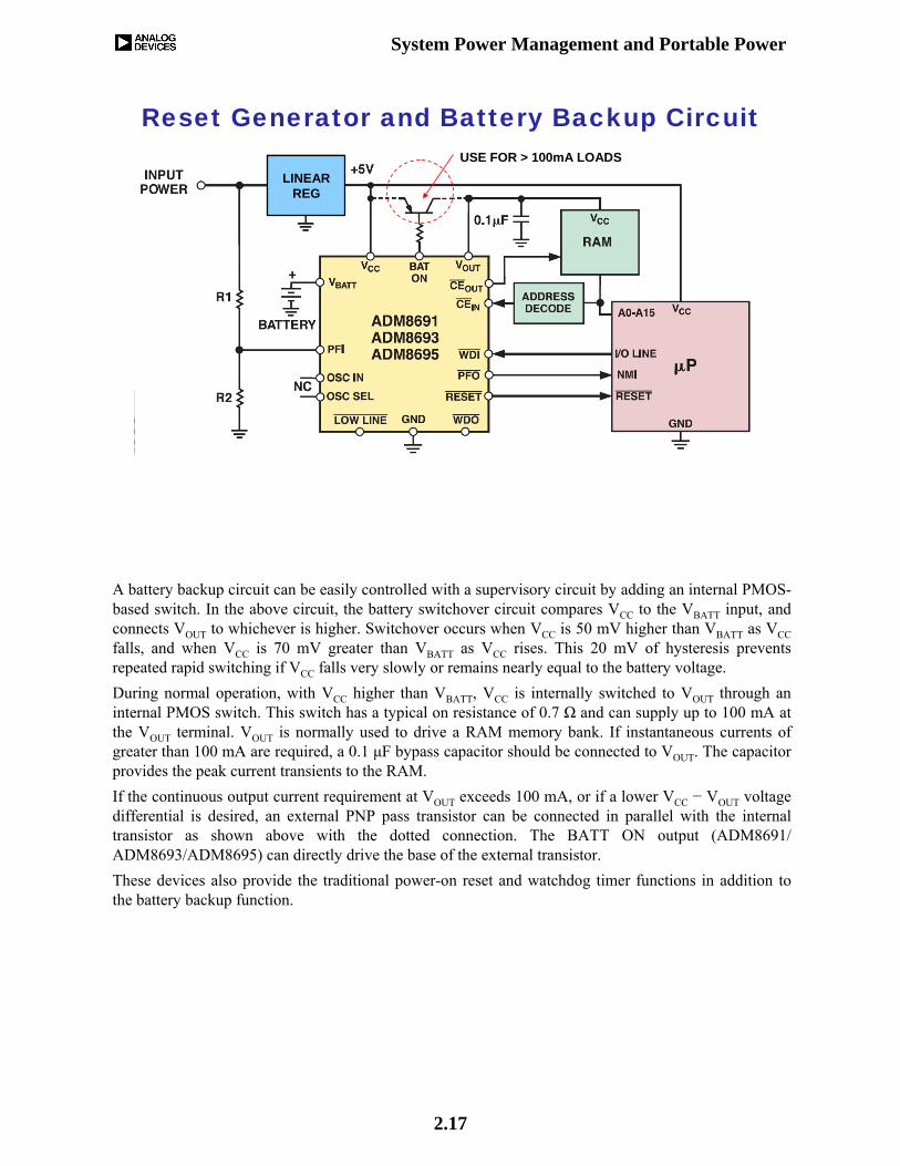
A battery backup circuit can be easily controlled with a supervisory circuit by adding an internal PMOS-based switch. In the above circuit, the battery switchover circuit compares VCC to the VBATT input, and connects VOUT to whichever is higher. Switchover occurs when VCC is 50 mV higher than VBATT as VCCfalls, and when VCC is 70 mV greater than VBATT as VCC rises. This 20 mV of hysteresis prevents repeated rapid switching if VCC falls very slowly or remains nearly equal to the battery voltage.During normal operation, with VCC higher than VBATT, VCC is internally switched to VOUT through an internal PMOS switch. This switch has a typical on resistance of 0.7 Ω and can supply up to 100 mA at the VOUT terminal. VOUT is normally used to drive a RAM memory bank. If instantaneous currents of greater than 100 mA are required, a 0.1 μF bypass capacitor should be connected to VOUT. The capacitor provides the peak current transients to the RAM. If the continuous output current requirement at VOUT exceeds 100 mA, or if a lower VCC − VOUT voltage differential is desired, an external PNP pass transistor can be connected in parallel with the internal transistor as shown above with the dotted connection. The BATT ON output (ADM8691/ ADM8693/ADM8695) can directly drive the base of the external transistor.These devices also provide the traditional power-on reset and watchdog timer functions in addition to the battery backup function.

System Power Management and Portable Power
2.18
On-Line Supervisory Parametric Search
Because of the wide variety of options available in supervisory products, some type of selection tool is mandatory in order to select the proper part for a specific application.The online Supervisory Parametric Search performs parametric searches on all Analog Devices supervisory products, both those currently available, and those that can be ordered. Searches can be performed on trip points, reset timeouts, watchdog timeouts, reset types, and other features. This figure shows the opening screen of the search function where the data is entered.In addition, a general ADI website tool provides cross-referencing between Analog Devices and competitive parts.

System Power Management and Portable Power
2.19
Results from Supervisory Parametric Search
After entering the inputs, the parametric search narrows the list of products based on the inputs. In this manner, the proper part can be easily chosen for a specific application.

System Power Management and Portable Power
2.20
Power Supply Monitoring and Sequencing
www.analog.com/sequencing
System Power Management and Portable Power
2.21
Comparators as Voltage MonitorsDISCRETE SOLUTION INTEGRATED SOLUTION WITH RESET
5VIN
3.3VIN
1.8VIN
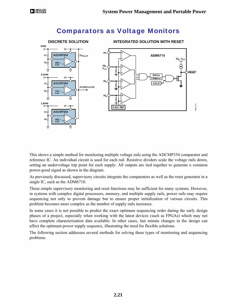
This shows a simple method for monitoring multiple voltage rails using the ADCMP354 comparator and reference IC. An individual circuit is used for each rail. Resistive dividers scale the voltage rails down, setting an undervoltage trip point for each supply. All outputs are tied together to generate a common power-good signal as shown in the diagram. As previously discussed, supervisory circuits integrate the comparators as well as the reset generator in a single IC, such as the ADM6710. These simple supervisory monitoring and reset functions may be sufficient for many systems. However, in systems with complex digital processors, memory, and multiple supply rails, power rails may require sequencing not only to prevent damage but to ensure proper initialization of various circuits. This problem becomes more complex as the number of supply rails increases. In some cases it is not possible to predict the exact optimum sequencing order during the early design phases of a project, especially when working with the latest devices (such as FPGAs) which may not have complete characterization data available. In other cases, last minute changes in the design can affect the optimum power supply sequence, illustrating the need for flexible solutions.The following section addresses several methods for solving these types of monitoring and sequencing problems.
System Power Management and Portable Power
2.22
Sequencing Supplies: I/O Before Core
IN
IN
OUT
OUT
EN
EN
DC-to-DC
DC-to-DC
12V IN5V IN
12V OUT5V OUT
3.3V OUT (I/O)
1.8V OUT (CORE)
R1
C1R2
C2
R3
C3
12 VOUT
5V OUT3.3V OUT (I/O)1.8V OUT (CORE)
tt1 t2 t3
SS
SS
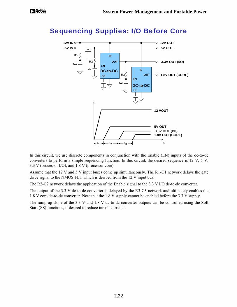
In this circuit, we use discrete components in conjunction with the Enable (EN) inputs of the dc-to-dc converters to perform a simple sequencing function. In this circuit, the desired sequence is 12 V, 5 V, 3.3 V (processor I/O), and 1.8 V (processor core).Assume that the 12 V and 5 V input buses come up simultaneously. The R1-C1 network delays the gate drive signal to the NMOS FET which is derived from the 12 V input bus.The R2-C2 network delays the application of the Enable signal to the 3.3 V I/O dc-to-dc converter.The output of the 3.3 V dc-to-dc converter is delayed by the R3-C3 network and ultimately enables the 1.8 V core dc-to-dc converter. Note that the 1.8 V supply cannot be enabled before the 3.3 V supply.The ramp-up slope of the 3.3 V and 1.8 V dc-to-dc converter outputs can be controlled using the Soft Start (SS) functions, if desired to reduce inrush currents.
System Power Management and Portable Power
2.23
Sequencing Supplies: Core Before I/O
IN
IN
OUT
OUT
EN
EN
DC-to-DC
DC-to-DC
12V IN5V IN
12V OUT5V OUT
1.8V OUT (CORE)
3.3V OUT (I/O)
R1
C1R2
C2
R3
C3
12V OUT
5V OUT3.3V OUT (I/O)1.8V OUT (CORE)
t1 t2 t3
SS
SS
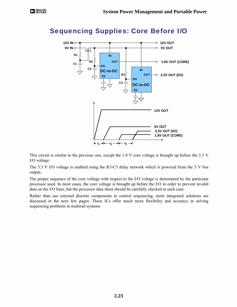
This circuit is similar to the previous one, except the 1.8 V core voltage is brought up before the 3.3 V I/O voltage.The 3.3 V I/O voltage is enabled using the R3-C3 delay network which is powered from the 5 V bus output. The proper sequence of the core voltage with respect to the I/O voltage is determined by the particular processor used. In most cases, the core voltage is brought up before the I/O in order to prevent invalid data on the I/O lines, but the processor data sheet should be carefully checked in each case. Rather than use external discrete components to control sequencing, more integrated solutions are discussed in the next few pages. These ICs offer much more flexibility and accuracy in solving sequencing problems in multirail systems.

System Power Management and Portable Power
2.24
Basic Sequencing Using ADM1085 Simple Sequencer® and Regulator Enables
SS SS SS SS
Here, three ADM1085 Simple Sequencers are used to sequence four individual supplies on power-up. The ADM1085 block diagram is also shown. The device consists of a comparator, capacitor-controlled adjustable delay, and an output stage, very similar to a microprocessor power-on reset circuit. The threshold voltage is set by the resistor divider which scales the particular supply voltage to the internal comparator reference voltage of 0.6 V. The positive-going threshold is 0.56 V to 0.64 V, and the negative-going threshold is 0.545 V to 0.645 V (over the operating temperature range of –40°C to +125°C). The accuracy of the 0.6 V threshold is approximately 7% over the full operating temperature range. The ADM1085 family of parts are in a 6-lead SC-70 package.The delay is determined by the value of the capacitor on the CEXT pin. Separate capacitors on the CEXT pins determine the time delays between enabling of the 3.3 V, 2.5 V, 1.8 V, and 1.2 V supplies. Because the dc-to-dc converters and ADM1085s are connected in a cascade, and the output of any converter is dependent on that of the previous one, an external controller can disable all four supplies simultaneously by disabling the first dc-to-dc converter in the chain.For power-down sequencing, an external controller dictates when the supplies are switched off by accessing the ENIN inputs individually. The ADM1085/ADM1086/ADM1087/ADM1088 are compatible with voltage regulators and dc-to-dc converters that have active high or active low enable or shutdown inputs, with a choice of open-drain or push-pull output stages. The sequence of the supplies is easily changed by simply changing the position of the dc-to-dc converter in the chain and adjusting the divider resistors appropriately. The dc-to-dc converter soft-start (SS) function can be used to control the individual power supply ramp rates if desired to reduce inrush currents.

System Power Management and Portable Power
2.25
ADM1185 Quad Voltage Monitor & Sequencer
4 Monitoring Comparators : 0.6V Reference, 0.8% AccurateTrip points set with external resistor dividers
VCC : 2.7V to 5.5V4 Open-Drain Outputs:
Three Enable Outputs for RegulatorsPower Good Output (PWRGD)
Logical Core:Provides power supply sequencing and fault detection
Package:10-lead MSOP Industry’s smallest Quad Sequencer
+-
+-
+-
+-
LOGICLOGIC
POWER AND REFERENCE GENERATOR
POWER AND REFERENCE GENERATOR
Ref=0.6V
0.6V
0.6V
0.6V
0.6V
VIN1
VIN2
VIN3
VIN4
VCC
OUT1
OUT2
OUT3
PWRGD
Rather than using an individual Simple Sequencer for each supply voltage as previously described, the ADM1185 allows monitoring and sequencing of up to four supplies. The part contains four individual comparators that are 0.8% accurate as well as a pre-programmed state machine for sequencing.The hardwired logical state machine core interprets the status of the comparator outputs. Internal time delays can be used for sequencing the startup of subsequent power supplies enabled by the outputs. Supplies falling out of range are also detected and, as a result, appropriate outputs are disabled. The ADM1185 has four open drain outputs. In a typical configuration, OUT1 to OUT3 are used to enable power supplies, while PWRGD is a common power-good output indicating the status of all monitored supplies, i.e., all four comparators are high. It is important to note that as processor core voltages decrease, the accuracy required to reliably monitor them increases. ADI provides voltage monitoring and sequencing products with accuracies as good as 0.8%.

System Power Management and Portable Power
2.26
1.2V OUT
ADM1185 Typical Monitoring & Sequencing Application
4 RAILS MONITORED
VIN1VIN2VIN3VIN4
OUT1
OUT2
OUT3
PWRGD
VCCADM1185
IN
EN OUT
Regulator 1
GNDIN
EN OUT
Regulator 2
GNDIN
EN OUT
Regulator 3
GND
3.3V IN
2.5V OUT1.8V OUT1.2V OUT 2.5V OUT
1.8V OUT
C1,2 DELAYC2,3 DELAY
3 REGULATORSSEQUENCED
This shows a typical application of the ADM1185 monitoring four supplies and sequencing three regulators. The resistor dividers scale the monitored voltages to equal the 0.6 V internal comparator reference voltage. External capacitors can be added in order to add more delay between the enabling of the regulators. OUT1 is an open-drain active high output. In this application, OUT1 is connected to the enable pin of Regulator 1. Before the voltage on VIN1 has reached 0.6 V, this output is switched to ground, disabling Regulator 1. Note that all outputs are driven to ground as long as there is at least 1 V on the VCC pin of the ADM1185. When the main system voltage reaches 2.9 V, VIN1 detects 0.6 V. This causes OUT1 to assert after a 190 ms (typical) delay. When this occurs, the open-drain output switches high, and the external pull-up resistor pulls the voltage on the Regulator 1 enable pin above its turn-on threshold, turning on the output of Regulator 1. The assertion of OUT1 turns on Regulator 1. The 2.5 V output of this regulator begins to rise. This is detected by input VIN2. When VIN2 detects the 2.5 V rail rising above its UV point, it asserts output OUT2, which turns on Regulator 2. A capacitor can be placed on the VIN2 pin to slow the rise of the voltage on this pin. This effectively sets a time delay between the 2.5 V rail powering up and the next regulator enable. The same scheme is implemented with the other input and output pins. Every rail that is turned on via an output pin, OUTx, is monitored via an input pin VIN(x + 1).The final comparator inside the VIN4 pin detects the final supply turning on, which is 1.2 V in this case. The output pins, OUT1 to OUT3, are logically AND'ed together to generate a system power-good signal (PWRGD). There is an internal 190 ms delay (typical) associated with the assertion of the PWRGD output.Note that the soft-start feature can be used if desired to control the output voltage ramp-up of any or all the regulators. Also, the regulators can be sequenced in any desired order by their placement in the chain with respect to OUT1, OUT2, and OUT3.
System Power Management and Portable Power
2.27
Timing Diagram for ADM1185
VIN1
OUT1
OUT2
PWRGD
tPROP
tPROP
tPROP
VT (RISING)
190ms
+ REG.3 DELAY190ms
190ms
OUT3
VT (RISING)VT (FALLING) = 0.6V
(A) POWER-UP (B) NEGATIVE-GOING GLITCH ON +3.3V
VIN1
OUT1
OUT2
PWRGD
OUT3
30µs + REG.1 DELAY+ C1,2 DELAY
30µs + REG.2 DELAY+ C2,3 DELAY
190ms
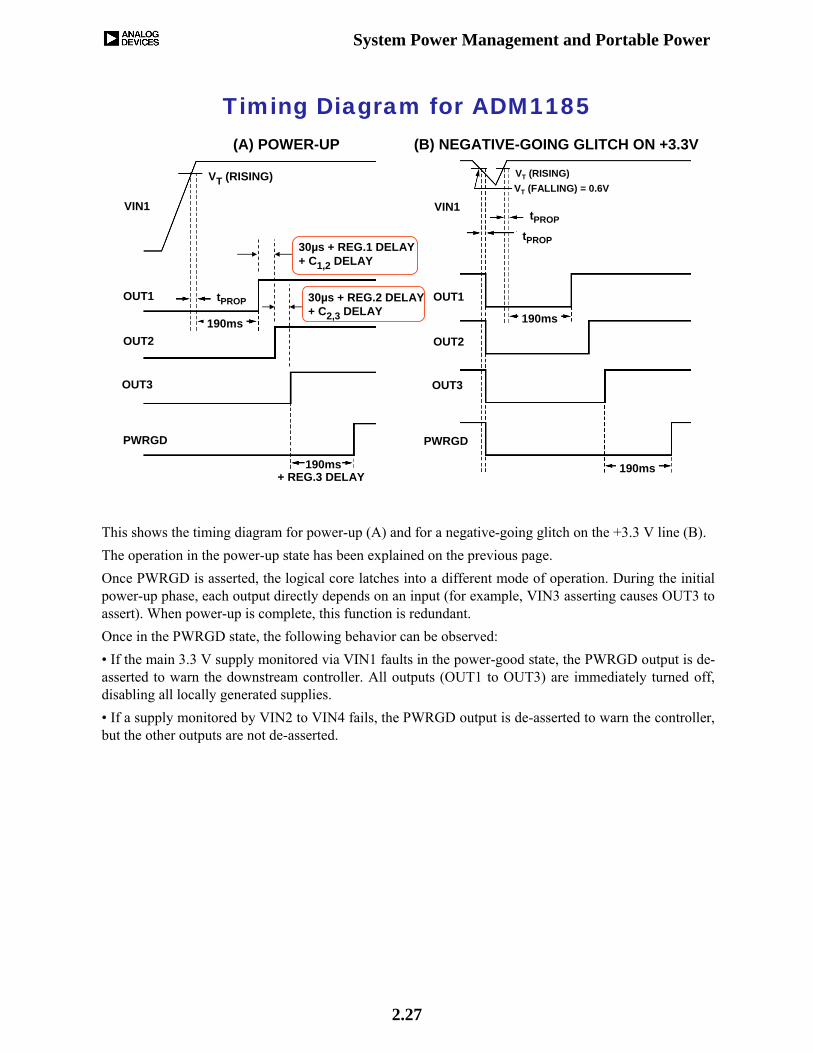
This shows the timing diagram for power-up (A) and for a negative-going glitch on the +3.3 V line (B). The operation in the power-up state has been explained on the previous page.Once PWRGD is asserted, the logical core latches into a different mode of operation. During the initial power-up phase, each output directly depends on an input (for example, VIN3 asserting causes OUT3 to assert). When power-up is complete, this function is redundant.Once in the PWRGD state, the following behavior can be observed:• If the main 3.3 V supply monitored via VIN1 faults in the power-good state, the PWRGD output is de-asserted to warn the downstream controller. All outputs (OUT1 to OUT3) are immediately turned off, disabling all locally generated supplies.• If a supply monitored by VIN2 to VIN4 fails, the PWRGD output is de-asserted to warn the controller, but the other outputs are not de-asserted.

System Power Management and Portable Power
2.28
ADM1066 Super Sequencer®
Sequencing more than three or four supply rails can become quite complex using individual sequencing ICs. Consider a system with eight voltage rails that requires a complex power-up sequence. Each rail must be monitored for undervoltage and overvoltage faults. In the event of a fault, all voltages could be turned off, or a power-down sequence could be initiated, depending on the failure mechanism. Actions must be taken depending upon the state of the control signals, and flags must be generated depending on the state of the power supplies. Implementing a circuit of this complexity with discrete devices and simple ICs may require hundreds of individual components, a huge amount of board space, and a significant combined cost. In systems with four or more voltages, it may make sense to use a centralized device to manage the power supplies. An example of this approach is shown above.The ADM106x Super Sequencer family continues to use comparators, but with some important differences. Two comparators are dedicated to each input so that undervoltage and overvoltage detection can be implemented, thus providing windowed monitoring for the rails. An undervoltage fault is the normal condition of a rail before it powers up, so this indication is used for sequencing. An overvoltage condition usually indicates a critical fault—such as a shorted FET or inductor—and calls for immediate action.Systems with higher supply counts usually have greater complexity, and thus have tighter accuracy constraints. Also, setting accurate thresholds with resistors becomes challenging at lower voltages, such as 1.0 V and 0.9 V. Although a 10% tolerance may be acceptable on a 5 V rail, this tolerance is generally insufficient on a 1 V rail. The ADM1066 allows input detector comparator thresholds to be set within 1% worst case, independent of the voltage (as low as 0.6 V)—and across the entire temperature range of the device. It adds internal glitch filtering and hysteresis to each comparator. Its logic inputs can be used to start the power-up sequence, shut down all rails, or perform other functions.

System Power Management and Portable Power
2.29
State Machine Based Sequencing Engine Core
The information from the bank of comparators is then fed into a powerful and flexible stage machine core and can be used for various purposes:1. Sequencing: When the output voltage of a recently enabled supply comes into a window, a time delay can be triggered to turn on the next rail in the power-up sequence. Complex sequencing, with multiple power-up and power-down sequences, or vastly different sequences for power-up and power-down is possible.2. Timeout: If a rail that has been enabled does not come on as expected, a suitable course of action can be taken (such as generating an interrupt or shutting down the system). A purely analog solution would simply hang at that point in the sequence. 3. Monitoring: If the voltage on any rail moves out of the preset window, a suitable course of action can be taken—depending on the rail that faulted, the type of fault that occurred, and the current operating mode. Systems with more than five supplies are often expensive, so comprehensive fault protection is crucial. An on-board charge pump is used to generate approximately 12 V of gate drive, even if the highest available system voltage is as low as 3 V, allowing outputs to directly drive series NMOS FETs. Additional outputs enable or shut down dc-to-dc converters or regulators, allowing an output to internally pull up to one of the inputs or the on-board regulated voltage. The outputs can also be asserted open-drain. Outputs may also be used as status signals such as power good or power-on reset. Status LEDs can be directly driven from the outputs if required.The state machine core is programmed via the industry-standard 2-wire SMBus interface.

System Power Management and Portable Power
2.30
ADM1066 Super Sequencer
The ADM1066 is a configurable supervisory/sequencing device that offers a single-chip solution for supply monitoring and sequencing in multiple-supply systems. In addition to these functions, the ADM1066 integrates a 12-bit ADC and six 8-bit voltage output DACs. These circuits can be used to implement a closed-loop margining system that enables supply adjustment by altering either the feedback node or reference of a dc-to-dc converter using the DAC outputs.Supply margining can be performed with a minimum of external components. The margining loop can be used for in-circuit testing of a board during production (for example, to verify the board’s functionality at −5% of nominal supplies), or can be used dynamically to accurately control the output voltage of a dc-to-dc converter.The device also provides up to 10 programmable inputs for monitoring under, over, or out-of-window faults on up to 10 supplies. In addition, 10 programmable outputs can be used as logic enables. Six of them can also provide up to a 12 V output for driving the gate of an NMOS FET, which can be placed in the path of a supply.The logical core of the device is a sequencing engine. This state-machine-based construction provides up to 63 different states. This design enables very flexible sequencing of the outputs, based on the condition of the inputs.The device is controlled via configuration data that can be programmed into an EEPROM. The whole configuration can be programmed using an intuitive GUI-based software package provided by Analog Devices, Inc. The on-board nonvolatile memory allows it to be reprogrammed as many times as necessary, while the sequencing and monitoring needs of the system evolve during the development process. This means that the hardware design can be completed early in the prototype process, and optimization of the monitoring and sequencing can be done as the project progresses.

System Power Management and Portable Power
2.31
Closed-Loop Supply MarginingUsing ADM1062/ADM1066
-
In addition to monitoring multiple voltage rails and providing a solution for complex sequencing, integrated power management devices, such as the ADM1066, also provide the tools to temporarily or permanently adjust individual rail voltages. The voltage output of a dc-to-dc converter or regulator can be altered by adjusting the voltage at the trim or feedback node of that device. Typically, a resistive divider between the output and ground of the module sets a nominal voltage at the trim/feedback pin. This, in turn, sets a nominal output voltage. Simple schemes involving switching extra resistors or controlling variable resistances in the feedback loop will alter the trim/feedback voltage and hence adjust the output voltage.The ADM1066 is equipped with digital-to-analog converters (DACs) to provide direct control over the trim/feedback node. For maximum efficiency, these DACs do not operate between ground and a maximum voltage; instead they operate across a relatively narrow window centered on the nominal trim/feedback level. The value of an attenuation resistor scales the incremental change in the output of the power module with each LSB change of the DAC. This open-loop adjustment provides margin-up and margin-down levels equivalent to those obtained by digital resistance switching in the reference circuit, and will adjust the output to a similar accuracy.The ADM1066 also includes a 12-bit analog-to-digital converter (ADC) to measure the supply voltages, so a closed-loop supply adjustment scheme can be implemented. With a given DAC output setting, the voltage output of the power module is digitized by the ADC and compared with the target voltage in software. The DAC can then be adjusted to calibrate the voltage output as closely as possible to the target voltage. This closed-loop scheme provides a very accurate method for supply adjustment. With a closed-loop method, the accuracy of the external resistors is completely irrelevant.
System Power Management and Portable Power
2.32
Hot Swap Controllers
www.analog.com/hotswap

System Power Management and Portable Power
2.33
What is a Hot Swap Controller?A Hot Swap Controller is a device which allows a removable circuit board to be removed or inserted into a live system without interrupting the system's power supply bus.Typical Backplane Bus Voltages: –48V, +12V, +5V
Hot swap controllers allow a circuit board to be removed or inserted into a live system without interrupting the system power supply bus.They are useful in many critical infrastructure applications such as telecommunications systems, servers, switchers and routers, and base stations—virtually any system which uses high currents and must remain operational while repairs, upgrades, or modifications are made. The standard backplane voltage for telecommunications is –48 V. This standard had its origins in the early days of the telephone network. The 48 V supply was considered to be the largest dc voltage that was not lethal under normal circumstances, and was a standard voltage easily generated by a battery backup bank made up of four 12 V batteries in series. The negative voltage was chosen to minimize galvanic corrosion causing corrosion of cables under damp conditions. A conductor with a negative charge will repel chlorine ions, as Cl (chlorine) ions are negative also. If the conductor were to have a positive charge, Cl ions would be attracted. This form of corrosion protection is called cathodic protection. It is often used for pipelines, bridges, etc. Such protection was very important in the days of open wire transmission lines.Other standard backplane voltages are +12 V and +5 V, and there are others.

System Power Management and Portable Power
2.34
Hot Swap TechniquesUsing short pin on connector
Provided delay on enabling Power Supply to eliminate arcing at connectors.
RC / Slew control on Power Supply SwitchThis allowed the voltage to increase slowly and hence charge capacitors slowly reducing inrush current spikes.
Some problems that remainedNo overcurrent protectionNo true inrush current protection—current limitedNo Short circuit protection
Benefits of Integrated Hot Swap controllersClosed Loop Accurate Current ControlTrue linear Soft Start controlProgrammable timing circuit breakerNMOS series-pass FETs
An early hot swap technique was to use a short pin on the connector for the power supply connection. This allowed all pins in the connector to be firmly in place before the actual power was applied, thereby minimizing arcing. Other techniques were used, such as RC slew-rate limiting on the power supply switch, but modern ICs allow the function to be performed much more reliably and seamlessly. Integrated hot swap controllers provide overcurrent protection, inrush current limiting, soft-start, and programmable timer controlled circuit breakers. The majority of IC hot swap controllers are designed to operate with low cost and highly reliable NMOS series pass FETs as the main power switching device.
System Power Management and Portable Power
2.35
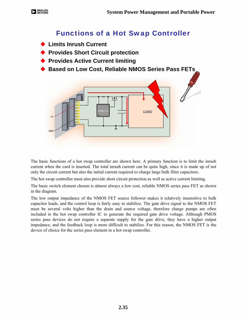
Functions of a Hot Swap ControllerLimits Inrush CurrentProvides Short Circuit protectionProvides Active Current limitingBased on Low Cost, Reliable NMOS Series Pass FETs
The basic functions of a hot swap controller are shown here. A primary function is to limit the inrush current when the card is inserted. The total inrush current can be quite high, since it is made up of not only the circuit current but also the initial current required to charge large bulk filter capacitors. The hot swap controller must also provide short circuit protection as well as active current limiting.The basic switch element chosen is almost always a low cost, reliable NMOS series pass FET as shown in the diagram. The low output impedance of the NMOS FET source follower makes it relatively insensitive to bulk capacitor loads, and the control loop is fairly easy to stabilize. The gate drive signal to the NMOS FET must be several volts higher than the drain and source voltage, therefore charge pumps are often included in the hot swap controller IC to generate the required gate drive voltage. Although PMOS series pass devices do not require a separate supply for the gate drive, they have a higher output impedance, and the feedback loop is more difficult to stabilize. For this reason, the NMOS FET is the device of choice for the series pass element in a hot swap controller.

System Power Management and Portable Power
2.36
Components of a Hot Swap Controller
VCP×20
This shows the basic components of a hot swap controller. The external components required are a sense resistor (RSENSE), NMOS FET switch, feedback compensation network (RG, RC, CC), voltage divider (RON1, RON2), and a timer capacitor (CTIMER). The voltage divider sets the threshold voltage to the internal comparator in the hot swap controller IC. In the case of the ADM4210, the comparator reference voltage is 1.3 V. the divider network shown divides the 5 V bus voltage by a factor of 3. In this circuit, the threshold voltage referenced to the bus voltage is 3 × 1.3 V = 3.9 V. The internal circuit breaker is controlled by a current sense comparator which starts an overcurrenttimeout sequence when the sense voltage is equal to 50 mV. The sense resistor limits the fault current to 50 mV/RSENSE. A sense resistor of 0.01 Ω gives a fault current of 5 A. The timing control circuit gives an initial timing delay of 273 ms/µF × CTIMER and a circuit breaker delay of 22 ms/µF × CTIMER. The timer generates ramp voltages by either sourcing or sinking current in or out of the CTIMER capacitor. The gate drive is turned on or off by two additional comparators and control logic. The internal comparator threshold voltages are 0.2 V and 1.3 V. The ADM4210 also contains a gate drive circuit for the external NMOS FET using an internal charge pump. The gate driver consists of a 12 µA pull-up current source from the internal charge pump voltage. The internal charge pump voltage range is typically 7.5 V to 11 V above VCC , for VCC between 3 V and 15 V.

System Power Management and Portable Power
2.37
How the Hot Swap Controller Works forNormal Power Up
Normal Power Up1. Controller is enabled
2. Timer Cycles Initial Period
3. Gate comes up
4. Inrush Current is Limited
5. Inrush Current falls off to normal
6. Power up complete
ON
TIMER
GATE
I LOAD
VOUT
12
3
45
6
This figure shows how a typical hot swap controller works for normal power up conditions.1. When the card is plugged in and the input voltage crosses the undervoltage lockout threshold, the controller is enabled, starting the internal timer.2. The timer voltage ramps up at a rate controlled be the external CTIMER capacitor and a pull-up current of 5 µA. 3. When the timer voltage reaches 1.3 V, this is the end of the first timing cycle. The timer current changes to a pull-down current of 100 µA, and the ramp voltage changes direction. When the ramp voltage reaches 0.2 V, the GATE pin is pulled high turning on the NMOS FET. 4. The second timer cycle is then enabled. When the voltage across the sense resistor exceeds the circuit breaker trip voltage, a timer pull-up current of 60 µA is activated. 5. If the sense voltage falls below the current limit level before the timer voltage reaches 1.3 V, the 60xμA pull-up is disabled and a 2 μA pull-down current is enabled. This is the normal operating mode if the overcurrent fault is only inrush current or a transient. 6. The 2 µA pull-down current causes the ramp voltage to return to zero, and the power-up cycle is completed.

System Power Management and Portable Power
2.38
How the Hot Swap Controller Works forPower Up Into a Fault
Power Up into a Fault1. Controller is enabled
2. Timer Cycles Initial Period
3. Gate comes up
4. Inrush Current is Limited
5. Current remains at limit due to Fault
6. Timer Expires and FET is Shutdown
FAULT
ON
TIMER
GATE
I LOAD
VOUT
12
3
4 5
6
6
This figure shows how the hot swap controller works when a card having a short circuit is plugged in.1. When the card is plugged in and the input voltage crosses the undervoltage lockout threshold, the controller is enabled, starting the internal timer.2. The timer voltage ramps up at a rate controlled be the external CTIMER capacitor and a pull-up current of 5 µA. 3. When the timer voltage reaches 1.3 V, this is the end of the first timing cycle. The timer current changes to a pull-down current of 100 µA, and the ramp voltage changes direction. When the ramp voltage reaches 0.2 V, the GATE pin is pulled high turning on the NMOS FET. 4. The second timer cycle then enabled. When the voltage across the sense resistor exceeds the circuit breaker trip voltage, a timer pull-up current of 60 µA is activated.5. The short circuit continues, and the ramp voltage reaches the 1.3 V threshold. The short circuit timer has now expired.6. The gate drive is pulled low, disabling the FET. On the ADM4210-1, the timer function activates the 2 μA pull-down once the 1.3 V threshold is reached, and continues to pull down until it reaches the 0.2 V threshold. At this point, the 100 μA pull-down is activated, and the GATE pin is enabled. The device then keeps retrying. The duty cycle of this automatic retry cycle is set to the ratio of 2 μA/60 μA, which approximates 3.8% on. The value of the timer capacitor determines the on-time of this cycle.The ADM4210-2 model has a latch-off system whereby when a current fault is detected, the GATE isswitched off after a time determined by the timer capacitor. Toggling the ON-CLR pin, or pulling the TIMER pin to GND for a brief period, resets this condition.
System Power Management and Portable Power
2.39
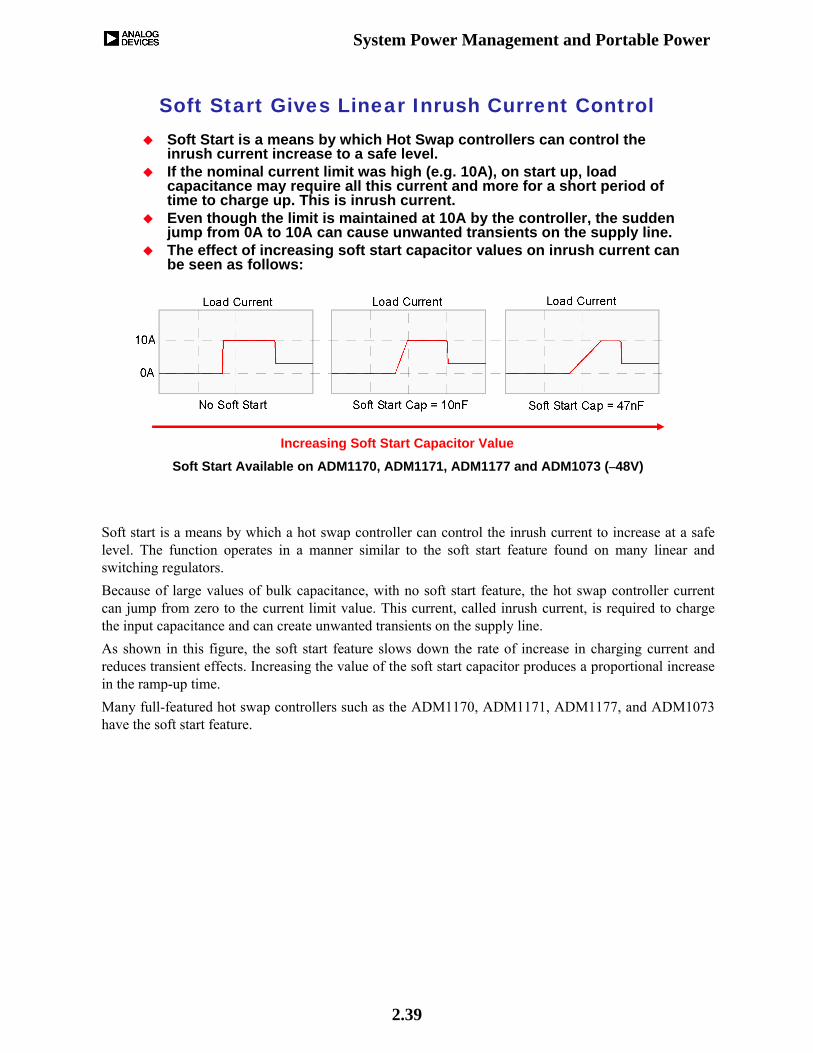
Soft Start Gives Linear Inrush Current ControlSoft Start is a means by which Hot Swap controllers can control the inrush current increase to a safe level.If the nominal current limit was high (e.g. 10A), on start up, load capacitance may require all this current and more for a short period of time to charge up. This is inrush current.Even though the limit is maintained at 10A by the controller, the sudden jump from 0A to 10A can cause unwanted transients on the supply line.The effect of increasing soft start capacitor values on inrush current can be seen as follows:
Increasing Soft Start Capacitor Value
Soft Start Available on ADM1170, ADM1171, ADM1177 and ADM1073 (–48V)
Soft start is a means by which a hot swap controller can control the inrush current to increase at a safe level. The function operates in a manner similar to the soft start feature found on many linear and switching regulators.Because of large values of bulk capacitance, with no soft start feature, the hot swap controller current can jump from zero to the current limit value. This current, called inrush current, is required to charge the input capacitance and can create unwanted transients on the supply line. As shown in this figure, the soft start feature slows down the rate of increase in charging current and reduces transient effects. Increasing the value of the soft start capacitor produces a proportional increase in the ramp-up time. Many full-featured hot swap controllers such as the ADM1170, ADM1171, ADM1177, and ADM1073 have the soft start feature.
System Power Management and Portable Power
2.40
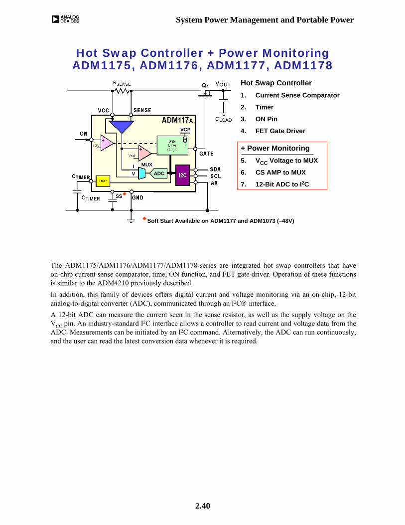
Hot Swap Controller + Power MonitoringADM1175, ADM1176, ADM1177, ADM1178
Hot Swap Controller1. Current Sense Comparator
2. Timer
3. ON Pin
4. FET Gate Driver
+ Power Monitoring5. VCC Voltage to MUX
6. CS AMP to MUX
7. 12-Bit ADC to I2C
VCP
MUXIV ADC
SS
Soft Start Available on ADM1177 and ADM1073 (–48V)
The ADM1175/ADM1176/ADM1177/ADM1178-series are integrated hot swap controllers that have on-chip current sense comparator, time, ON function, and FET gate driver. Operation of these functions is similar to the ADM4210 previously described. In addition, this family of devices offers digital current and voltage monitoring via an on-chip, 12-bit analog-to-digital converter (ADC), communicated through an I2C® interface.A 12-bit ADC can measure the current seen in the sense resistor, as well as the supply voltage on the VCC pin. An industry-standard I2C interface allows a controller to read current and voltage data from the ADC. Measurements can be initiated by an I2C command. Alternatively, the ADC can run continuously, and the user can read the latest conversion data whenever it is required.

System Power Management and Portable Power
2.41
ADM117x/ADM119x Solution for Digital Power Measurement
12V 5V
3.3VA 3.3VB
Advantages of Localized Sensing
Local DigitizationMinimizes NoiseSimple Bus Routing
-+
ADC
ADM117xADM119x
-+
ADC
ADM117xADM119x
ADC
ADM117xADM119x
+ -
ADC
ADM117xADM119x
+ -
Power = V x I
µP(I2C MASTER)
I2C Bus
Digital Current+ Voltage
Digital Current+ Voltage
Digital Current + Voltage
Digital Current + Voltage
As well as performing the hot swap function, the ADM1175/ADM1176/ADM1177/ADM1178-series can monitor total power consumed by each PC board via the on-chip ADC and the I2C bus. Noise is minimized by performing the digitization locally on each PC board and transmitting the current and voltage measurements digitally, rather than transmitting the actual PC board voltages and the current-sense signals over system wiring. The ADM1191 and ADM1192 perform the power monitoring function, but without the hot swap feature.

System Power Management and Portable Power
2.42
Temperature Monitoring
www.analog.com/temperature

System Power Management and Portable Power
2.43
THERMOCOUPLE RTD THERMISTOR SEMICONDUCTOR
Widest Range:
–184ºC to +2300ºC
Range:
–200ºC to +850ºC
Range:
0ºC to +100ºC
Range:
–55ºC to +150ºC
High Accuracy and
Repeatability
Fair Linearity Poor Linearity Linearity: 1ºC
Accuracy: 1ºC
Needs Cold Junction
Compensation
Requires
Excitation
Requires
Excitation
Requires Excitation
Low-Voltage Output Low Cost High Sensitivity 10mV/K, 20mV/K,
or 1µA/K Typical Output
Types of Temperature Sensors
Measurement of temperature is critical in modern electronic devices, especially expensive computers with densely packed circuits which dissipate considerable power in the form of heat. Knowledge of system temperature can also be used to control battery charging as well as prevent damage to expensive microprocessors. Compact high power portable equipment often has fan cooling to maintain junction temperatures at proper levels. In order to conserve battery life, the fan should only operate when necessary. Accurate control of the fan requires a knowledge of critical temperatures from the appropriate temperature sensor.Accurate temperature measurements are required in many other measurement systems such as process control and instrumentation applications. In most cases, because of low-level nonlinear outputs, the sensor output must be properly conditioned and amplified before further processing can occur. Thermocouples have the widest temperature range of all the sensors, but require specialized signal conditioning circuitry because of their low-level outputs and non-linear transfer functionsResistance Temperature Devices (RTDs) are accurate, but require excitation current and are generallyused in bridge circuits. Thermistors have the most sensitivity but are the most non-linear. However, they are popular in portable applications such as measurement of battery temperature and other critical temperatures in a system. Modern semiconductor temperature sensors offer high accuracy and high linearity over an operating range of about –55ºC to +150ºC. Internal amplifiers can scale the output to convenient values, such as 10xmV/ºC. Semiconductor temperature sensors can be integrated into multi-function ICs which perform a number of other hardware monitoring functions, and are ideal for most system applications where temperature is critical.

System Power Management and Portable Power
2.44
Basic Relationship for IC Temperature Sensors
IC IC
VBE VN
ΔVBE VBE VNkTq
N= − = ln( )
VBEkTq
ICIS
=⎛⎝⎜
⎞⎠⎟ln VN
kTq
ICN IS
=⋅
⎛⎝⎜
⎞⎠⎟ln
INDEPENDENT OF IC, IS
ONE TRANSISTORN TRANSISTORS
Modern semiconductor temperature sensors offer high accuracy and high linearity over an operating range of about –55°C to +150°C. All semiconductor temperature sensors make use of the relationship between a bipolar junction transistor's (BJT) base-emitter voltage to its collector current:
where k is Boltzmann's constant, T is the absolute temperature (K), q is the charge of an electron, and Isis a current related to the geometry and the temperature of the transistors. (The equation assumes a voltage of at least a few hundred mV on the collector, and ignores Early effects.)If we take N transistors identical to the first and allow the total current Ic to be shared equally among them, we find that the new base-emitter voltage is given by the equation
Neither of these circuits is of much use by itself because of the strongly temperature dependent current Is, but if we have equal currents in one BJT and N similar BJTs then the expression for the difference between the two base-emitter voltages is proportional to absolute temperature and does not contain Is:
VBE
kTq
IcIs
=⎛⎝⎜
⎞⎠⎟ln
VN
kTq
IcN Is
=⋅
⎛⎝⎜
⎞⎠⎟ln
VBE VNkTq
IcIs
IcN Is
kTq
N− =
⎛⎝⎜
⎞⎠⎟
⋅⎛⎝⎜
⎞⎠⎟
⎡
⎣
⎢⎢⎢⎢
⎤
⎦
⎥⎥⎥⎥
=ln ln( )

System Power Management and Portable Power
2.45
Classic Band Gap Temperature Sensor
"BROKAW CELL"R R
+I2 ≅ I1
Q2NA
Q1A
R2
R1
VN VBE(Q1)
VBANDGAP = 1.205V
+VIN
VPTAT = 2 R1R2
kTq ln(N)
ΔVBE VBE VNkTq
N= − = ln( )
The circuit shown in this figure implements the previous equation and is known as the "Brokaw Cell". The voltage VBE – VN appears across resistor R2. The emitter current in Q2 is therefore (VBE – VN)/R2. The op amp's servo loop and the resistors, R, force the same current to flow through Q1. The Q1 and Q2 currents are equal and are summed and flow into resistor R1. The corresponding voltage developed across R1 is proportional to absolute temperature (PTAT) and given by:
The band gap cell reference voltage, VBANDGAP, appears at the base of Q1 and is the sum of VBE(Q1) and VPTAT. VBE(Q1) is complementary to absolute temperature (CTAT), and summing it with VPTAT causes the band gap voltage to be constant with respect to temperature (assuming proper choice of R1/R2 ratio and N to make the band gap voltage equal to 1.205 V). This circuit is the basic band gap temperature sensor, and is widely used in semiconductor temperature sensors.
( )VPTATVBE VNR
RR
kTq
N=−
=2R1
22 1
2ln( )

System Power Management and Portable Power
2.46
Analog Temperature Sensors are Now Integrated into Many Different Parts
TEMPSENSOR
VPTAT
COMPARATORSOR ADC
SWITCHSETPOINT CONTROLLER PWMSPI, I2C, SMBus
DIGITAL OUTPUTS
TEMPSENSOR
VPTAT
DATA ACQUISITION SYSTEMPRECISION ANALOG MICROCONTROLLERSINTEGRATED SET POINT CONTROLLERS
TEMPERATURE-TO-DIGITAL CONVERTERS
INTEGRATED SOLUTIONS THAT INCLUDE TEMPERATURE SENSOR
Voltage references form an integral part of data acquisition systems of all types. The VPTAT voltage is conveniently part of the reference and is available for temperature sensing as well. It is therefore relatively easy to integrate a temperature sensor into most modern ICs if one is required. The sensor monitors the temperature of its junction, which should be approximately equal to the ambient temperature, provided the total internal power dissipation of the device is low, and self-heating is not an issue. Digital temperature sensors can take many forms. The simplest is a VPTAT generator followed by a comparator which acts as a simple on/off function, depending on the comparator voltage reference. This type of temperature sensor forms the basis of modern setpoint controllers. More sophisticated digital temperature sensors use an ADC to convert the temperature sensor voltage into either a PWM signal, or bus-compatible digital signal.

System Power Management and Portable Power
2.47
Low Cost, 2.7V to 5.5V, MicropowerTemperature Switches in SOT-23
ADT6502
FROM 12-BIT SIGMA-DELTA MODULATOR
The ADT6501/ADT6502/ADT6503/ADT6504 are trip point temperature switches available in a 5-lead SOT-23 package. Each part contains an internal band gap temperature sensor for local temperature sensing. The band gap output voltage (VPTAT) is digitized with a 12-bit sigma-delta modulator. The 12-bit output from the modulator is input into a digital comparator where it is compared with a factory set trip level. The output trip pin is activated if the temperature measured is greater than the factory set trip level. Overall accuracy for the ADT650x family is ±6°C from −45°C to +115°C.Factory set trip levels are available in 10°C increments from +35°C to +115°C for the ADT6501/ADT6502 and from –45°C to +15°C for the ADT6503/ADT6504. The ADT6501/ADT6503 logic output is active low and open-drain. The ADT6502/ADT6504 logic output is active high and push-pull. The temperature is digitized to a resolution of 0.0625°C (12 bit). The factory settings are 10°C apart starting from −45°C to +15°C for the cold threshold models and from +35°C to +115°C for the hot threshold models.These devices require no external components and typically consume 30 μA supply current. Hysteresis is pin-selectable at 2°C and 10°C. The temperature switch is specified to operate over the supply range of 2.7 V to 5.5 V.The ADT6501 and ADT6502 are used for monitoring temperatures from +35°C to +115°C only. Therefore, the logic output pin becomes active when the temperature goes higher than the selected trip point temperature.The ADT6503 and ADT6504 are used for monitoring temperatures from −45°C to +15°C only. Therefore, the logic output pin becomes active when the temperature goes lower than the selected trip point temperature.The circuit shown uses the ADT6502 and an external NMOS FET to drive a fan. The output of the ADT6502 goes high when the temperature goes higher than the selected trip point temperature, turning on the FET and the fan.
System Power Management and Portable Power
2.48
Digital Isolation and Isolated Power
www.analog.com/icoupler

System Power Management and Portable Power
2.49
Digital Isolators Based on iCoupler® Technology
Digital isolators are extremely useful in separating system grounds. Designed primarily for galvanic isolation in industrial applications, the iCoupler isolator can be used to pass signals between ground planes at different potentials. No currents will circulate through the various grounds, since we are using transformers to isolate the grounds. The transfer rate through the iCoupler can be as high as 100 Mbps.The ADuM140x1 are 4-channel digital isolators based on Analog Devices, Inc. iCoupler technology. Combining high speed CMOS and monolithic air core transformer technology, these isolation components provide outstanding performance characteristics superior to alternatives such as optocouplerdevices.By avoiding the use of LEDs and photodiodes, iCoupler devices remove the design difficulties commonly associated with optocouplers. The typical optocoupler concerns regarding uncertain current transfer ratios, nonlinear transfer functions, and temperature and lifetime effects are eliminated with the simple iCoupler digital interfaces and stable performance characteristics.The need for external drivers and other discrete components is eliminated with these iCoupler products. Furthermore, iCoupler devices consume one-tenth to one-sixth the power of optocouplers at comparable signal data rates and are more cost effective.The ADuM140x isolators provide four independent isolation channels in a variety of channel configurations and data rates. All models operate with the supply voltage on either side ranging from 2.7xV to 5.5 V, providing compatibility with lower voltage systems as well as enabling a voltage translation functionality across the isolation barrier. Unlike other optocoupler alternatives, the ADuM140x isolators have a patented refresh feature that ensures dc correctness in the absence of input logic transitions and during power-up/power-down conditions.

System Power Management and Portable Power
2.50
Construction of the iCoupler Digital Isolator
CMOS INTERFACE CHIPS CONTAINDRIVE AND RECEIVE CIRCUITS
20µm POLYIMIDEINSULATIONWITHSTANDS>5kV ISOLATION
TRANSFORMERCOILS TRANSMITDATA IN BOTHDIRECTIONS
This photo shows a 4-channel digital isolator, which houses three die in a single package. Two CMOS interface circuits (left and right) integrate drive and receive electronics. The middle die contains four chip-scale microtransformers, each comprising metal (AlCu and Au) coils on either side of a 20 µm polyimide insulation layer. The polyimide is capable of withstanding more than 5 kV rms for one minute. In most applications that require isolated data transmission, isolated power must be available on both sides of the isolation barrier, or it must be provided separately. System designers typically introduce isolated power by designing an isolated power supply using discrete components—including a transformer with the appropriate isolation rating—or by purchasing a commercial off-the-shelf isolated dc-to-dc converter. Each approach has its advantages and disadvantages. In the first instance, isolated power supplies may be custom tailored to an application, allowing system designers to optimize their cost, isolation rating, power output, or other important specifications depending on the application requirements. The downside, however, is that custom solutions tend to be bulky, require safety certification, and can lengthen development times. Commercially available isolated power supplies, on the other hand, can reduce time to market, but they carry a price penalty and may not be optimized to fit a particular application. While smaller in size than their custom counterparts, they are still fairly bulky, with only limited availability of surface-mount package options.A third way is isoPower®, which combines the benefits of both options. iCoupler digital isolators condition and drive data across the transformers. isoPower uses the same chip-scale microtransformertechnology, but instead of transmitting only data, isoPower employs switches, rectifiers, and regulators to generate power that is isolated to the same degree as the data channels.

System Power Management and Portable Power
2.51
Unidirectional and Bidirectional Transmission(A)
(B)
(C) I2C BUS FOR BIDIRECTIONAL COMMUNICATIONS
In isolation, the term bidirectional has traditionally referred to an isolator with separate transmit and receive channels in one package—the isolator as a whole is capable of bidirectional data transfer, but the individual channels are unidirectional as shown in (A). This approach is compatible with communications protocols such as RS-232, RS-485, and SPI, but it is not compatible with true bidirectional communication protocols, such as I2C, SMBus, and PMBus, which support bidirectional data transfer through a single channel as shown in (B). The inter-integrated-circuit (I2C) bus is a popular 2-wire, bidirectional communication protocol that was developed to provide simple, low-cost, short-distance communication between an on-board controller and its peripherals. I2C buses limit the cost of applications in which multiple devices share a single bus with a host controller, as shown in (C). Two bidirectional wires—one for the data and one for the clock—are used to achieve low cost at the expense of data rate, so I2C is typically used in systems with many peripherals running at data rates less than 1 Mbps. Systems that use a limited number of peripherals running at higher data rates will often employ protocols such as SPI.

System Power Management and Portable Power
2.52
iCoupler Simplifies True Bidirectional Isolation
(A) OPTOCOUPLER SOLUTION (B) iCOUPLER SOLUTION
The I2C isolation challenge has been that optocouplers are based on diodes that can transmit in only one direction, and are therefore inherently unidirectional. A bidirectional I2C bus could be isolated using optocouplers as shown in (A), but the implementation is messy. A special buffer is used to separate each bidirectional channel into two distinct channels: transmit and receive. Once separated, the four unidirectional channels can be individually isolated and then recombined. This solution requires four isolators and expands the bus from two wires to four wires. Additional circuitry is also required, making this solution costly and large, and defeating the original purpose of the 2-wire bus implementation: to save money and space.The good news is that by adopting the new digital isolation techniques the circuitry that is used to separate, isolate, and recombine the data channels can be integrated into a single package. This approach can be implemented with the new ADuM1250 and ADuM1251 hot-swappable dual I2C isolators. Figure (B) illustrates how much more compact the iCoupler solution is.

System Power Management and Portable Power
2.53
True Bidirectional Isolation Using the ADuM1250 Digital Isolator
This figure shows how bidirectional isolation is achieved within the package. Just as the discrete solution employs a buffer to separate the two bidirectional channels into four unidirectional channels and four isolators, so, too, does the ADuM125x family. The difference is that all the electronics are integrated onto a single IC. A designer sees only the 2-wire interface, and the entire device is less than 40 mm2, a 90% reduction compared with the optocoupler/buffer solution, which takes up about 350xmm2.The ADuM125x family operates at rates up to 1 MHz.

System Power Management and Portable Power
2.54
ADuM5240 Dual-Channel Isolator with isoPower Integrated DC-to-DC Converter
In addition to digital isolation, the capability of providing isolated power is important in many applications. The ADuM524x are dual-channel digital isolators with isoPower integrated, isolated power. An on-chip dc-to-dc converter provides up to 50 mW of regulated, isolated power at 5 V, which eliminates the need for a separate isolated dc-to-dc converter in low power isolated designs. The ADuM524x isolators provide two independent isolation channels in a variety of channel configurations, operating from a 5 V input supply. ADuM524x units may be used in combination with other iCoupler products to achieve greater channel counts.The ADuM524x family of isolators operates at data rates up to 1 Mbps.

System Power Management and Portable Power
2.55
isoPower Digital Isolator Implements Isolated Power
This figure shows the isolated power section of the ADuM5240, ADuM5241, and ADuM5242 the first iCoupler products with isoPower. Four cross-coupled CMOS switches generate an ac waveform that drives the transformer. On the isolated side, Schottky diodes rectify the ac signal. The rectified signal is passed to a linear regulator, which maintains the output voltage at a nominal 5 V setpoint. The output is capable of supplying 10 mA of current. The chip-scale microtransformers are made from 6 μm thick gold, separated by a 20 μm polyimide insulation layer, which is capable of providing greater than 5 kV rms isolation. Because the transformer coils, only 600 mm in diameter, have a low L/R ratio compared with conventional transformers, high-efficiency power generation requires high-frequency switching—on the order of 300 MHz. As noted earlier, the transformers used to generate power employ the same process as those used to isolate data. The only significant difference between data and power channels is the conditioning circuitry on either side of the isolation barrier.
System Power Management and Portable Power
2.56
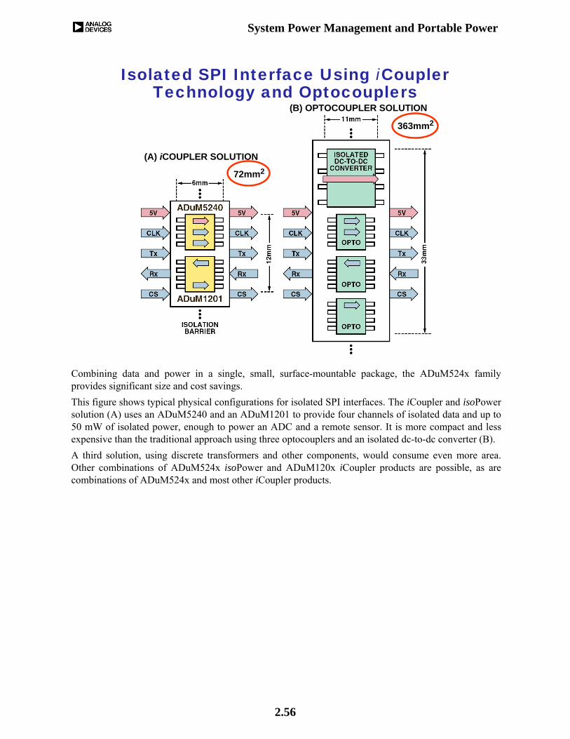
Isolated SPI Interface Using iCouplerTechnology and Optocouplers
(A) iCOUPLER SOLUTION
(B) OPTOCOUPLER SOLUTION
72mm2
363mm2
Combining data and power in a single, small, surface-mountable package, the ADuM524x family provides significant size and cost savings. This figure shows typical physical configurations for isolated SPI interfaces. The iCoupler and isoPowersolution (A) uses an ADuM5240 and an ADuM1201 to provide four channels of isolated data and up to 50 mW of isolated power, enough to power an ADC and a remote sensor. It is more compact and less expensive than the traditional approach using three optocouplers and an isolated dc-to-dc converter (B).A third solution, using discrete transformers and other components, would consume even more area. Other combinations of ADuM524x isoPower and ADuM120x iCoupler products are possible, as are combinations of ADuM524x and most other iCoupler products.

System Power Management and Portable Power
2.57
Completely Isolated Turbidity Sensor and ADC
DOUT
ISOLATED POWER
ISOLATED 3-WIREINTERFACE
This figure shows a completely isolated turbidity sensor system that measures the amount of particulates in a liquid solution and can be used to determine the cleanliness of a volume of water. They are increasingly being used in home appliances, such as dishwashers and washing machines, both to conserve water and to improve cleaning performance. Conventional appliances wash or rinse for a set time, overestimating the required level of cleaning to ensure that the load is fully clean at the end of the cycle. A turbidity sensor, however, can let the system know when to stop cleaning. The machine will use the optimal amount of water for the optimal time, thus minimizing waste while maximizing useful cleaning performance.Because turbidity sensors must be immersed in the water, they present two challenges to an appliance designer. First, the sensor must be small enough to fit unobtrusively anywhere within the space where clothes or dishes are to be placed. The size of the sensor is, therefore, critical. Second, the powered circuit is immersed in water, so the sensor must be safely isolated from the rest of the system. If the physical insulation should fail, the user and the system electronics must not be harmed, and there must be no possibility of fire. Both the power and the data must therefore be isolated.This figure demonstrates a cost-effective solution. The AD7823 low-power 8-bit 200 kSPS SAR ADC uses a 3-wire interface to convert the analog output of a turbidity sensor. The digitized turbidity data is transmitted across the galvanic isolation barrier of the ADuM1200 and ADuM5242. The 50 mW of isolated power from the ADuM5242 is sufficient to supply the ADuM1200, the AD7823, and the turbidity sensor. The combined area of the isolators and converter is less than 100 mm2, excluding external components.

System Power Management and Portable Power
2.58
Digital Power Applications

System Power Management and Portable Power
2.59
Digital Power Management andDigital Power Control
Digital Power ManagementVoltage MonitoringSequencingMarginingTemperature Monitoring and Fan ControlSupervisionCommunication via data bus (SMBus, I2C, PMBus)
Digital Power ControlReal-time control of a power converter using an ADC and digital techniques within a feedback loop
REF
We have seen how digital techniques are currently being used in voltage monitoring, sequencing, margining, temperature monitoring, fan control supervision, etc. These applications fall into the broad area loosely defined as digital power management. Although the results obtained through digital techniques (generally comparators or ADCs) may be used to control various system parameters, there is no real-time feedback loop in the classic sense of feedback control systems (operational amplifiers, servo systems, process control, etc.). Digital power control, on the other hand, refers specifically to the real-time control of a power converter (ac-to-dc or dc-to-dc) using an ADC and digital techniques (digital filter, for example) within a feedback loop as shown above. As is usually the case, the digital approach offers many advantages (neglecting the economic factor for the moment).Currently most point-of-load switching converters use analog techniques to control output voltage. There is no technical reason why the digital techniques illustrated above can't be used. The slow migration to digital power control is mostly due to economic factors. The digital implementation is simply more costly using today's CMOS process technology. Digital control is, however, beginning to appear in the high power primary-side ac-to-dc converters and in secondary-sided dc-to-dc converters, where the requirements and economics make digital control an attractive alternative to traditional analog techniques. As digital processes continue to shrink (analog processes do too, but not as rapidly), digital control will eventually progress further downstream in the power chain.

System Power Management and Portable Power
2.60
Digital Control Loop FeaturesIntegration of all typical controller functions
Remote and local voltage sense Both primary and secondary side current sensePWM control Synchronous Rectifier controlDigital or Analog Current Share Bus
Digital Control LoopIntegrated filterFilter can be adapted through software
Easier to maintain phase margin with voltage-mode controllersFaster development timeFaster debuggingOption to compensate for temperature
Programmability through I2CDigital control currently used in AC-to-DC primary-side converters and DC-to-DC secondary-side converters
ADC technology in CMOS has progressed rapidly. The requirement for ADCs in digital power control is approximately 12 bits at sampling rates of a few MHz. This will obviously change due to product improvements, but represents the current requirement in primary and secondary-side power converters. Other than increased reliability, functionality, power density, efficiency, reduced component count, etc., digital control offers design flexibility in the feedback control loop compensation. Current point-of-load supplies designed for powering high power microprocessors (such as Intel and AMD) are often manually adjusted on the system board for optimum load current step response. Digital adaptive feedback loop control and timing should eliminate this need.Most analog switching converters use voltage-mode (VM), current-mode (CM), or a combination of the two in order to determine the value of feedback compensation values. Proper compensation of the feedback loop in order to maintain adequate phase margin in both the continuous conduction mode (CCM) and discontinuous conduction mode (DCM) is somewhat complicated. This is especially difficult when using only voltage-mode control. In a digital feedback control loop, the compensation is performed by digital filters whose characteristics can be easily changed depending on the mode of operation. This means that VM control is practical using adaptive digital filter techniques.
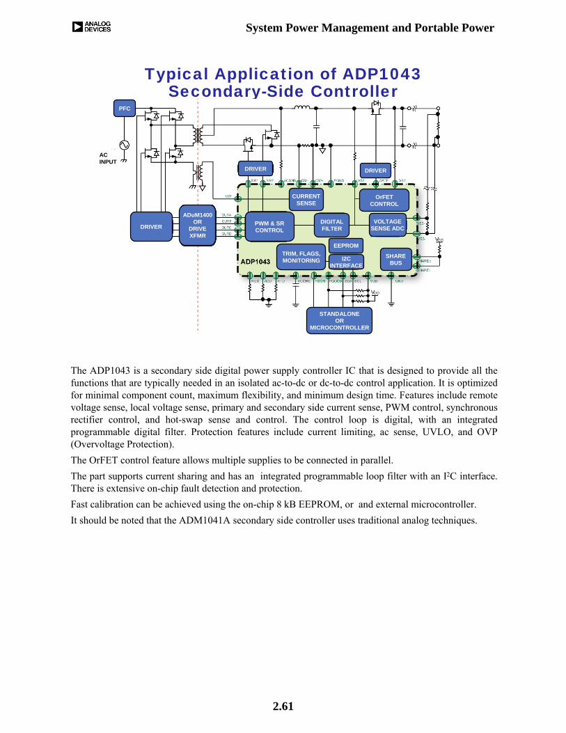
System Power Management and Portable Power
2.61
Typical Application of ADP1043Secondary-Side Controller
PFC
DRIVER
ADuM1400OR
DRIVEXFMR
CURRENTSENSE
PWM & SRCONTROL
TRIM, FLAGS,MONITORING
DIGITALFILTER
OrFETCONTROL
VOLTAGESENSE ADC
EEPROM
I2CINTERFACE
SHAREBUS
DRIVER DRIVER
DRIVER
PFC
ACINPUT
STANDALONEOR
MICROCONTROLLER
The ADP1043 is a secondary side digital power supply controller IC that is designed to provide all the functions that are typically needed in an isolated ac-to-dc or dc-to-dc control application. It is optimized for minimal component count, maximum flexibility, and minimum design time. Features include remote voltage sense, local voltage sense, primary and secondary side current sense, PWM control, synchronous rectifier control, and hot-swap sense and control. The control loop is digital, with an integrated programmable digital filter. Protection features include current limiting, ac sense, UVLO, and OVP (Overvoltage Protection).The OrFET control feature allows multiple supplies to be connected in parallel. The part supports current sharing and has an integrated programmable loop filter with an I2C interface. There is extensive on-chip fault detection and protection. Fast calibration can be achieved using the on-chip 8 kB EEPROM, or and external microcontroller. It should be noted that the ADM1041A secondary side controller uses traditional analog techniques.
System Power Management and Portable Power
2.62
Programmability and Monitoring(Through I2C)
Output Voltage SettingOvercurrent (OCP) limitOvervoltage (OVP) limitUndervoltage (UVP) limitOvertemperature (OTP) limitSoft-Start & Soft-Stop timingLoop filter poles and gainsPWM timingDuty cycle limitsOrFET On/Off trip voltage
Output currentOutput voltageOutput Line ImpedanceInput currentOutput powerDuty cycleCurrent share busTemperature
PROGRAMMABILITY MONITORING
The use of the I2C bus provides both programmability and monitoring functions. This figure lists some of the various functions included by each.

System Power Management and Portable Power
2.63
PoweringPortable Systems

System Power Management and Portable Power
2.64
Portable Power ConsiderationsBattery technology
Lithium Ion battery of choiceNiMH and NiCd being phased out
Maximize battery life!Sleep and low power modesNeed efficient, small, low cost buck, boost, and buck-boost regulators as well as LDOs
Digital cameras, cell phones, PDAs, etc. require custom-tailored solutions
Modern portable systems depend highly on battery technology and efficient power management techniques. Maximizing battery life is a prime concern of portable equipment manufacturers.Average power reduction techniques such as sleep, standby, or idle modes are required as well as efficient, small, low cost regulators. Buck, boost, and buck-boost switching regulators as well as LDOs must be carefully integrated into the power chain of a portable system. In many cases, a custom-tailored power management IC is required for the specific application.

System Power Management and Portable Power
2.65
The Energy System:Lithium Ion (Li-Ion)
DIS
CH
AR
GE
VOLT
AG
E (V
)
NNP = Nickel-Based New Platform, Matsushita Battery Industrial Co., LTD
By far the most popular battery technology for today's portable systems is Lithium-Ion (Li-Ion). The discharge curve is shown here. New technology (NNP) extends the capacity of the battery and is available. "NNP" is an abbreviation for Nickel-Based New Platform Lithium-ion technology from Matsushita Battery Industrial Co., LTD. Work is on-going to produce even greater capacity in Li-Ion batteries.The discharge curve shown here indicates that the usable battery voltage for current technology Li-Ion extends from 4.2V (fully charged) to 3.0 V (discharged). This means that the portable system power supply must provide the necessary output voltages over this fairly wide input voltage range. If the electronics require a 3.3 V supply, then it is clear that a buck-boost regulator is needed as the input voltage discharges from 4.2 V to 3.0 V. The new Li-Ion technology discharges to 2.5 V, thereby lowering the usable battery voltage and increasing the probability of needing a buck-boost regulator.

System Power Management and Portable Power
2.66
Techniques for Portable PowerEf
ficie
ncy
Load Current
Typical Conditions: VIN = Li-Ion Battery = 3.0 V (2.5 V, NNP) to 4.2 V VOUT = 1.8 V
150mA 200mA 800mA
95%
60%
85%
40%Linear
Low EfficiencySmall SizeLow CostLow Noise
Inductive DC-to-DC Buck, Boost or Buck-Boost
Highest EfficiencyLargest SizeHigh CostHigh Noise
Switched CapacitorMedium EfficiencySmall SizeMedium CostMedium Noise
There are three popular techniques for supplying portable power systems. The following guidelines apply specifically to a system powered by a single Li-Ion battery where the voltage ranges from 4.2 V to 3.0 V (2.5 V for NNP technology), and the output voltage is approximately 1.8 V. The inductive dc-to-dc buck, boost, or buck-boost regulator is the most efficient for higher currents, but takes up the most space and is generally the most costly of the three. Also the noise is the greatest.The switched capacitor ("inductorless") regulator has medium efficiency, smaller size, lower cost, and less noise than the inductive regulators. However, the current capability is limited to approximately 200xmA. The linear regulator (almost always an LDO) is by far the easiest to apply, the smallest, and has the lowest cost and noise of the three types. The efficiency of the LDO is approximately VOUT/VIN, so making general statements about their usage is somewhat dangerous. In applications where the VIN –VOUT voltage is low, the LDO may be an ideal choice if the current requirement is relatively low. We will now look at a few typical applications in portable systems and see how efficient use can be made of the available power management building blocks.

System Power Management and Portable Power
2.67
Processor Power Distribution with Separate Core and I/O Voltage
VIO
RESET
VCORE
PF
VDDOUT
VINVOFB
EN
VINVO
FBEN
µPORDSP
VIO = 1.8V TO 2.5V
ADP2105
ADP2108
VOLTAGESUPERVISOR
EN_VIO
EN_VCORE
Li-IonBATTERY
VCORE = 1.0V TO 1.8V
VBATT = 3.0V to 4.2V
ADP2102: VIN = 2.7V to 5.5V, VOUT = 0.8V to 3.3V, 0.6A, 3MHzADP2105: VIN = 2.7V to 5.5V, VOUT = 0.8V to 3.3V, 1.0A, 1.2MHzADP2106: VIN = 2.7V to 5.5V, VOUT = 0.8V to 3.3V, 1.5A, 1.2MHzADP2107: VIN = 2.7V to 5.5V, VOUT = 0.8V to 3.3V, 2.0A, 1.2MHzADP2108: VIN = 2.3V to 5.5V, VOUT = 1.0V to 3.3V, 0.6A, 3MHz
A common example in portable systems is generating the power for a microprocessor or DSP from a single Li-ion battery. As in "fixed" power applications, most modern microprocessors and DSPs for portable systems require a separate I/O and core voltage. In this application, the ADP2105 synchronous buck regulator generates the I/O voltage which can be between 1.8 V and 2.5 V depending on the processor. The maximum current output is 1 A. The ADP2108 would also work if the current requirement is less than 600 mA. The 1.0 V to 1.8 V core voltage is supplied by the ADP2108 synchronous buck regulator which can handle up to 600 mA.
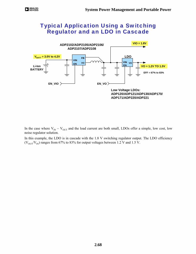
System Power Management and Portable Power
2.68
Typical Application Using a Switching Regulator and an LDO in Cascade
VINVO
FB
EN
LDOVIN VOENLi-Ion
BATTERY
ADP2102/ADP2105/ADP2106/ADP2107/ADP2108
EN_VIO
VIO = 1.8V
VO = 1.2V TO 1.5V
EN_VO
VBATT = 3.0V to 4.2V
EFF = 67% to 83%
Low Voltage LDOs:ADP120/ADP121/ADP130/ADP170/ADP171/ADP220/ADP221
In the case where VIN – VOUT and the load current are both small, LDOs offer a simple, low cost, low noise regulator solution. In this example, the LDO is in cascade with the 1.8 V switching regulator output. The LDO efficiency (VOUT/VIN) ranges from 67% to 83% for output voltages between 1.2 V and 1.5 V.

System Power Management and Portable Power
2.69
Point-of-Use Regulation Using LDOswith Low VIN – VOUT
ADP210xSwitchingRegulator
VBATT = 3.0Vto 4.2V
1.0V LDO
1.2V LDO
1.5V LDO
VOUT = 1.8V
Efficiency improves from27-40% to 55-83% by Operating LDOs on 1.8VLow Voltage LDOs: ADP120/ADP121/ADP130/ADP170/ADP171/ADP220/ADP221
Memory/IO’s
LDO EFF = 1.5/1.8 = 83%
LDO EFF = 1.2/1.8 = 67%
LDO EFF = 1.0/1.8 = 55%
VIN = 3.7LDO EFF = 1.0/3.7 = 27%
Li-IonBATTERY
In this application, LDOs are driven from the ADP210x switching regulator 1.8 V output and provide efficiencies between 55% and 83% for output voltages between 1.0 V and 1.5 V.Without the intermediate bus voltage of 1.8 V, the 1.0 V LDO efficiency drops to 27% if driven directly from the Li-Ion battery with a nominal voltage of 3.7 V.
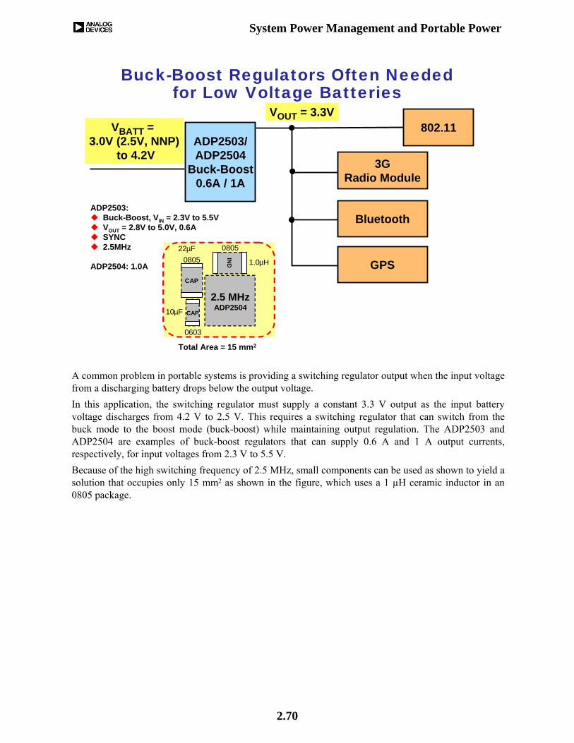
System Power Management and Portable Power
2.70
Buck-Boost Regulators Often Needed for Low Voltage Batteries
ADP2503/ADP2504
Buck-Boost0.6A / 1A
VBATT = 3.0V (2.5V, NNP)
to 4.2V
GPS
Bluetooth
3GRadio Module
VOUT = 3.3V802.11
ADP2503: Buck-Boost, VIN = 2.3V to 5.5V VOUT = 2.8V to 5.0V, 0.6ASYNC2.5MHz
ADP2504: 1.0A
Total Area = 15 mm2
0603
0805
1.0µH
IND
2.5 MHzADP2504
CAP
080522µF
CAP10µF
0603
0805
1.0µH
IND
IND
2.5 MHzADP2504
CAP
080522µF
CAP10µF
A common problem in portable systems is providing a switching regulator output when the input voltage from a discharging battery drops below the output voltage. In this application, the switching regulator must supply a constant 3.3 V output as the input battery voltage discharges from 4.2 V to 2.5 V. This requires a switching regulator that can switch from the buck mode to the boost mode (buck-boost) while maintaining output regulation. The ADP2503 and ADP2504 are examples of buck-boost regulators that can supply 0.6 A and 1 A output currents, respectively, for input voltages from 2.3 V to 5.5 V. Because of the high switching frequency of 2.5 MHz, small components can be used as shown to yield a solution that occupies only 15 mm2 as shown in the figure, which uses a 1 µH ceramic inductor in an 0805 package.

System Power Management and Portable Power
2.71
Integrated Camera Module Solution
9.6/19.2MHz
APPLICATIONPROCESSOR
xSHTSDA SCL DN
xSHTSD SCL DN
xSHTSDA SCL DN
xSHTDN SDA SCL
ADP5020 IMAGESENSOR
LENSDRIVER
SYNC
VDD_IO
GPIO/EN
VDDx
VLDO
VBUCK/BOOST
VBUCK
VIO
2.8V3.3V
SYNC
MOTOR
2.8V
MICRO-CONTROLLER
SDA SCL
Driver
LENS
VIO1.8V 2.5V-2.8V
@ 100mA
3.3V@ 400mA
1.2V-1.8V@200mA
VCORE+
BATTERY:2.3V TO 5V SYNCHRONOUS BUCK
H-BRIDGE BUCK/BOOSTLDO
This figure shows an integrated power solution for a camera module. The ADP5020 controller provides the following outputs:
1. 3.3 V, 400 mA buck-boost output based on an H-bridge FET controller.2. 1.2 V to 1.8 V buck output capable of 200 mA for core voltage.3. 2.5 V to 2.8 V 100 mA LDO output.
The device operates on an input voltage range of 2.3 V to 5.0 V, thereby covering all popular battery types.The internal switching frequency of the regulators is 3 MHz.The digital interface is I2C.The figure shows the interface of the ADP5020 with the application process, image sensor, lens driver, and microcontroller.

System Power Management and Portable Power
2.72
ADP1653 Flash LED Driver RequiresBoost Regulator
LED Current can be set by resistor or I2C
ILEDVBAT
An excellent example of a boost regulator application is in a flash LED driver. The system typically operates on a single Li-ion battery (3.0 V to 4.2 V), but at least 7.5 V is required for the diode bias voltage. Flash systems generally use two LEDs in series, so the total voltage drop across the two diodes in the flash mode is 3.6 × 2 = 7.2 V. The current source shown in the figure needs a headroom of 0.3 V, so the total diode bias voltage required is 7.5 V. This voltage is generated by the ADP1653 boost regulator. The LED current can be set by a resistor or programmed using the I2C interface. The ADP1653 is a very compact, high efficiency, high power, camera-flash LED driver optimized for cellular phones. The device’s high efficiency and dynamic LED current control improve flash brightness and picture quality in dimly lit environments. Efficiency peaks at 92% and is higher than charge pump solutions over the Li-ion battery range.The device has a dual-mode interface that is configurable to 2-bit logic or an I2C interface. The indicator LED and high power LED currents are programmable with external resistors or through the I2C interface. To maximize overall flash brightness, the ADP1653 offers an input to reduce flash LED current in less than 50 μs, referred to as the Tx mask. Tx masking reduces battery stress by scaling back flash LED current during an RF transmission.The ADP1653 solution requires only four external components in I2C mode and fits in a 6.4 mm ×7.2xmm space. The part integrates multiple safety features such as soft start, flash timeout, output current limit, thermal protection, and overvoltage protection.

System Power Management and Portable Power
2.73
Basic Switched Capacitor VoltageInverter and Voltage Doubler
VOUT ≈ –VIN
LOAD
VIN+
C1 C2
IOUT
INVERTER
VOUT ≈ 2VIN
LOAD
VIN+
C1 C2
IOUTDOUBLER
We have seen how inductors can be used to transfer energy and perform voltage conversions. This section examines switched capacitor voltage converters which accomplish energy transfer and voltage conversion using capacitors. The two most common switched capacitor voltage converters are the voltage inverter and the voltage doubler circuit shown in the figure. In the voltage inverter, the charge pump capacitor, C1, is charged to the input voltage during the first half of the switching cycle. During the second half of the switching cycle, its voltage is inverted and applied to capacitor C2 and the load. The output voltage is the negative of the input voltage, and the average input current is approximately equal to the output current. The switching frequency impacts the size of the external capacitors required, and higher switching frequencies allow the use of smaller capacitors. The duty cycle—defined as the ratio of charging time for C1 to the entire switching cycle time—is usually 50%, because that generally yields the optimal chargetransfer efficiency. After initial start-up transient conditions and when a steady-state condition is reached, the charge pump capacitor only has to supply a small amount of charge to the output capacitor on each switching cycle. The amount of charge transferred depends upon the load current and the switching frequency. During the time the pump capacitor is charged by the input voltage, the output capacitor C2 must supply the load current. The load current flowing out of C2 causes a droop in the output voltage which corresponds to a component of output voltage ripple. Higher switching frequencies allow smaller capacitors for the same amount of droop. There are, however, practical limitations on the switching speeds and switching losses, and switching frequencies are generally limited to a few hundred kHz. The voltage doubler works similarly to the inverter; however, the pump capacitor is placed in series with the input voltage during its discharge cycle, thereby accomplishing the voltage doubling function. In the voltage doubler, the average input current is approximately twice the average output current.

System Power Management and Portable Power
2.74
ADP3605 120mA Switched Capacitor Inverter with Regulated Output
RON CONTROL
By far the simplest and most effective method for achieving regulation in a switched capacitor voltage converter is to use an error amplifier to control the on-resistance of one of the switches as shown in this figure, a block diagram of the ADP3605 120 mA voltage inverter. This device offers a regulated –3 V output for an input voltage of +3 V to +6 V. The output is sensed and fed back into the device via the VSENSE pin. Output regulation is accomplished by varying the on-resistance of one of the MOSFET switches as shown by the control signal labeled "RON CONTROL" in the diagram. This signal accomplishes the switching of the MOSFET as well as controlling the on-resistance.
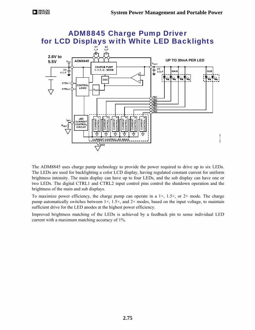
System Power Management and Portable Power
2.75
ADM8845 Charge Pump Driver for LCD Displays with White LED Backlights
2.6V to5.5V UP TO 30mA PER LED
The ADM8845 uses charge pump technology to provide the power required to drive up to six LEDs. The LEDs are used for backlighting a color LCD display, having regulated constant current for uniform brightness intensity. The main display can have up to four LEDs, and the sub display can have one or two LEDs. The digital CTRL1 and CTRL2 input control pins control the shutdown operation and the brightness of the main and sub displays.To maximize power efficiency, the charge pump can operate in a 1×, 1.5×, or 2× mode. The charge pump automatically switches between 1×, 1.5×, and 2× modes, based on the input voltage, to maintain sufficient drive for the LED anodes at the highest power efficiency.Improved brightness matching of the LEDs is achieved by a feedback pin to sense individual LED current with a maximum matching accuracy of 1%.

System Power Management and Portable Power
2.76
Technical References

System Power Management and Portable Power
2.77
Analog Devices' Technical References1. Hank Zumbahlen, Basic Linear Design, Analog Devices, 2006, ISBN: 0-915550-28-1.
Also available as Linear Circuit Design Handbook, Elsevier-Newnes, 2008, ISBN-10: 0750687037, ISBN-13: 978-0750687034. See Chapter 9.
2. Walt Kester, Analog-Digital Conversion, Analog Devices, 2004, ISBN: 0916550273. Also available as Data Conversion Handbook, Elsevier-Newnes, 2005, ISBN: 0750678410. See Chapter 7.
3. Walt Jung, Op Amp Applications, Analog Devices, 2002, ISBN: 0-916550-26-5. Also available as Op Amp Applications Handbook, Elsevier-Newnes, 2004, ISBN: 0-7506-7844-5. See Chapter 7.
4. Sridhar Gurram, Oliver Brennan, Tim Wilkerson, "DC-to-DC Switching-Regulator Insights—Achieving Longer Battery Life in DSP Systems," Analog Dialogue 41-12, December 2007.