Embed Size (px)
Citation preview

G522-0290-00 MPCFPE/AD1/97
REV. 1
PowerPC
™
Microprocessor Family:
The Programming Environments

© Motorola Inc. 1997. All rights reserved.Portions hereof © International Business Machines Corp. 1991–1997. All rights reserved.
This document contains information on a new product under development by Motorola and IBM. Motorola and IBM reserve the right to change ordiscontinue this product without notice. Information in this document is provided solely to enable system and software implementers to use PowerPCmicroprocessors. There are no express or implied copyright or patent licenses granted hereunder by Motorola or IBM to design, modify the design of, orfabricate circuits based on the information in this document.
The PowerPC microprocessor embodies the intellectual property of Motorola and of IBM. However, neither Motorola nor IBM assumes any responsibilityor liability as to any aspects of the performance, operation, or other attributes of the microprocessor as marketed by the other party or by any third party.Neither Motorola nor IBM is to be considered an agent or representative of the other, and neither has assumed, created, or granted hereby any right orauthority to the other, or to any third party, to assume or create any express or implied obligations on its behalf. Information such as errata sheets anddata sheets, as well as sales terms and conditions such as prices, schedules, and support, for the product may vary as between parties selling the product.Accordingly, customers wishing to learn more information about the products as marketed by a given party should contact that party.
Both Motorola and IBM reserve the right to modify this document and/or any of the products as described herein without further notice.
NOTHING INTHIS DOCUMENT, NOR IN ANY OF THE ERRATA SHEETS, DATA SHEETS, AND OTHER SUPPORTING DOCUMENTATION, SHALL BEINTERPRETED AS THE CONVEYANCE BY MOTOROLA OR IBM OF AN EXPRESS WARRANTY OF ANY KIND OR IMPLIED WARRANTY,REPRESENTATION, OR GUARANTEE REGARDING THE MERCHANTABILITY OR FITNESS OF THE PRODUCTS FOR ANY PARTICULARPURPOSE
. Neither Motorola nor IBM assumes any liability or obligation for damages of any kind arising out of the application or use of these materials.Any warranty or other obligations as to the products described herein shall be undertaken solely by the marketing party to the customer, under a separatesale agreement between the marketing party and the customer. In the absence of such an agreement, no liability is assumed by Motorola, IBM, or themarketing party for any damages, actual or otherwise.
“Typical” parameters can and do vary in different applications. All operating parameters, including “Typicals,” must be validated for each customerapplication by customer’s technical experts. Neither Motorola nor IBM convey any license under their respective intellectual property rights nor the rightsof others. Neither Motorola nor IBM makes any claim, warranty, or representation, express or implied, that the products described in this document aredesigned, intended, or authorized for use as components in systems intended for surgical implant into the body, or other applications intended to supportor sustain life, or for any other application in which the failure of the product could create a situation where personal injury or death may occur. Shouldcustomer purchase or use the products for any such unintended or unauthorized application, customer shall indemnify and hold Motorola and IBM andtheir respective officers, employees, subsidiaries, affiliates, and distributors harmless against all claims, costs, damages, and expenses, and reasonableattorney’s fees arising out of, directly or indirectly, any claim of personal injury or death associated with such unintended or unauthorized use, even if suchclaim alleges that Motorola or IBM was negligent regarding the design or manufacture of the part.
Motorola and are registered trademarks of Motorola, Inc. Motorola, Inc. is an Equal Opportunity/Affirmative Action Employer.
IBM, the IBM logo, IBM Microelectronics, RS/6000, and System/370 are trademarks of International Business Machines Corporation.The PowerPC name, the PowerPC logotype, PowerPC 601, PowerPC 602, PowerPC 603, PowerPC 603e, PowerPC 604, PowerPC 604e, and PowerPC620 are trademarks of International Business Machines Corporation used by Motorola under license from International Business Machines Corporation.International Business Machines Corporation is an Equal Opportunity/Affirmative Action Employer.

Overview
PowerPC Register Set
Operand Conventions
Addressing Modes and Instruction Set Summary
Cache Model and Memory Coherency
Exceptions
Memory Management
Instruction Set
PowerPC Instruction Set Listings
POWER Architecture Cross Reference
Multiple-Precision Shifts
Floating-Point Models
Synchronization Programming Examples
Simplified Mnemonics
Glossary of Terms and Abbreviations
Index
1
2
3
4
5
6
8
7
A
B
C
D
E
F
IND
GLO

Overview
PowerPC Register Set
Operand Conventions
Addressing Modes and Instruction Set Summary
Cache Model and Memory Coherency
Exceptions
Memory Management
Instruction Set
PowerPC Instruction Set Listings
POWER Architecture Cross Reference
Multiple-Precision Shifts
Floating-Point Models
Synchronization Programming Examples
Simplified Mnemonics
Glossary of Terms and Abbreviations
Index
A
B
C
D
E
F
2
3
4
5
6
1
8
7
IND
GLO

Contents
iii
CONTENTS
ParagraphNumber Title Page
Number
About This Book
Audience ............................................................................................................ xxixOrganization....................................................................................................... xxixSuggested Reading...............................................................................................xxxConventions ..................................................................................................... xxxiiiAcronyms and Abbreviations .......................................................................... xxxivTerminology Conventions .............................................................................. xxxvii
Chapter 1
Overview
1.1 PowerPC Architecture Overview......................................................................... 1-21.1.1 The 64-Bit PowerPC Architecture and the 32-Bit Subset ............................... 1-41.1.2 The Levels of the PowerPC Architecture ........................................................ 1-51.1.3 Latitude Within the Levels of the PowerPC Architecture ............................... 1-71.1.4 Features Not Defined by the PowerPC Architecture ....................................... 1-81.1.5 Summary of Architectural Changes in this Revision....................................... 1-91.2 The PowerPC Architectural Models .................................................................. 1-101.2.1 PowerPC Registers and Programming Model ............................................... 1-101.2.2 Operand Conventions .................................................................................... 1-111.2.2.1 Byte Ordering ............................................................................................ 1-111.2.2.2 Data Organization in Memory and Data Transfers.................................... 1-121.2.2.3 Floating-Point Conventions ....................................................................... 1-121.2.3 PowerPC Instruction Set and Addressing Modes .......................................... 1-121.2.3.1 PowerPC Instruction Set............................................................................ 1-131.2.3.2 Calculating Effective Addresses................................................................ 1-151.2.4 PowerPC Cache Model.................................................................................. 1-151.2.5 PowerPC Exception Model............................................................................ 1-161.2.6 PowerPC Memory Management Model ........................................................ 1-161.3 Changes in This Revision of The Programming Environments Manual ........... 1-181.3.1 General Changes to the PowerPC Architecture............................................. 1-191.3.2 Changes Related to the Optional 64-Bit Bridge ............................................ 1-19

iv
PowerPC Microprocessor Family: The Programming Environments, Rev. 1
CONTENTS
ParagraphNumber Title Page
Number
Chapter 2
PowerPC Register Set
2.1 PowerPC UISA Register Set................................................................................ 2-12.1.1 General-Purpose Registers (GPRs).................................................................. 2-32.1.2 Floating-Point Registers (FPRs) ...................................................................... 2-42.1.3 Condition Register (CR) .................................................................................. 2-52.1.3.1 Condition Register CR0 Field Definition .................................................... 2-62.1.3.2 Condition Register CR1 Field Definition .................................................... 2-62.1.3.3 Condition Register CR
n
Field—Compare Instruction ................................ 2-72.1.4 Floating-Point Status and Control Register (FPSCR)...................................... 2-72.1.5 XER Register (XER) ..................................................................................... 2-112.1.6 Link Register (LR)......................................................................................... 2-112.1.7 Count Register (CTR).................................................................................... 2-122.2 PowerPC VEA Register Set—Time Base.......................................................... 2-132.2.1 Reading the Time Base .................................................................................. 2-162.2.1.1 Reading the Time Base on 64-Bit Implementations.................................. 2-162.2.1.2 Reading the Time Base on 32-Bit Implementations.................................. 2-162.2.2 Computing Time of Day from the Time Base ............................................... 2-172.3 PowerPC OEA Register Set............................................................................... 2-172.3.1 Machine State Register (MSR) ...................................................................... 2-202.3.2 Processor Version Register (PVR) ................................................................ 2-242.3.3 BAT Registers................................................................................................ 2-252.3.4 SDR1.............................................................................................................. 2-282.3.5 Address Space Register (ASR) ...................................................................... 2-302.3.6 Segment Registers.......................................................................................... 2-312.3.7 Data Address Register (DAR) ....................................................................... 2-332.3.8 SPRG0–SPRG3 ............................................................................................. 2-332.3.9 DSISR ............................................................................................................ 2-342.3.10 Machine Status Save/Restore Register 0 (SRR0) .......................................... 2-342.3.11 Machine Status Save/Restore Register 1 (SRR1) .......................................... 2-352.3.12 Floating-Point Exception Cause Register (FPECR) ...................................... 2-362.3.13 Time Base Facility (TB)—OEA.................................................................... 2-362.3.13.1 Writing to the Time Base........................................................................... 2-362.3.14 Decrementer Register (DEC)......................................................................... 2-372.3.14.1 Decrementer Operation.............................................................................. 2-372.3.14.2 Writing and Reading the DEC................................................................... 2-382.3.15 Data Address Breakpoint Register (DABR).................................................. 2-382.3.16 External Access Register (EAR).................................................................... 2-392.3.17 Processor Identification Register (PIR) ......................................................... 2-402.3.18 Synchronization Requirements for Special Registers and
for Lookaside Buffers ................................................................................ 2-40
Contents
v
CONTENTS
ParagraphNumber Title Page
Number
Chapter 3
Operand Conventions
3.1 Data Organization in Memory and Data Transfers.............................................. 3-13.1.1 Aligned and Misaligned Accesses ................................................................... 3-13.1.2 Byte Ordering .................................................................................................. 3-23.1.2.1 Big-Endian Byte Ordering........................................................................... 3-23.1.2.2 Little-Endian Byte Ordering ........................................................................ 3-33.1.3 Structure Mapping Examples........................................................................... 3-33.1.3.1 Big-Endian Mapping ................................................................................... 3-43.1.3.2 Little-Endian Mapping................................................................................. 3-53.1.4 PowerPC Byte Ordering .................................................................................. 3-63.1.4.1 Aligned Scalars in Little-Endian Mode ....................................................... 3-63.1.4.2 Misaligned Scalars in Little-Endian Mode .................................................. 3-93.1.4.3 Nonscalars.................................................................................................. 3-103.1.4.4 PowerPC Instruction Addressing in Little-Endian Mode.......................... 3-103.1.4.5 PowerPC Input/Output Data Transfer Addressing in Little-Endian Mode 3-113.2 Effect of Operand Placement on Performance—VEA ...................................... 3-123.2.1 Summary of Performance Effects.................................................................. 3-123.2.2 Instruction Restart.......................................................................................... 3-143.3 Floating-Point Execution Models—UISA......................................................... 3-153.3.1 Floating-Point Data Format ........................................................................... 3-163.3.1.1 Value Representation................................................................................. 3-183.3.1.2 Binary Floating-Point Numbers................................................................. 3-193.3.1.3 Normalized Numbers (
±
NORM)............................................................... 3-193.3.1.4 Zero Values (
±
0)........................................................................................ 3-203.3.1.5 Denormalized Numbers (
±
DENORM)...................................................... 3-203.3.1.6 Infinities (
±∞
) ............................................................................................ 3-213.3.1.7 Not a Numbers (NaNs) .............................................................................. 3-213.3.2 Sign of Result................................................................................................. 3-223.3.3 Normalization and Denormalization.............................................................. 3-233.3.4 Data Handling and Precision ......................................................................... 3-243.3.5 Rounding........................................................................................................ 3-253.3.6 Floating-Point Program Exceptions............................................................... 3-283.3.6.1 Invalid Operation and Zero Divide Exception Conditions ........................ 3-353.3.6.1.1 Invalid Operation Exception Condition................................................. 3-373.3.6.1.2 Zero Divide Exception Condition.......................................................... 3-383.3.6.2 Overflow, Underflow, and Inexact Exception Conditions ........................ 3-393.3.6.2.1 Overflow Exception Condition.............................................................. 3-413.3.6.2.2 Underflow Exception Condition............................................................ 3-423.3.6.2.3 Inexact Exception Condition ................................................................. 3-43
vi
PowerPC Microprocessor Family: The Programming Environments, Rev. 1
CONTENTS
ParagraphNumber Title Page
Number
Chapter 4
Addressing Modes and Instruction Set Summary
4.1 Conventions ......................................................................................................... 4-24.1.1 Sequential Execution Model............................................................................ 4-34.1.2 Computation Modes......................................................................................... 4-34.1.2.1 64-Bit Implementations ............................................................................... 4-34.1.2.2 32-Bit Implementations ............................................................................... 4-44.1.3 Classes of Instructions ..................................................................................... 4-44.1.3.1 Definition of Boundedly Undefined ............................................................ 4-44.1.3.2 Defined Instruction Class ............................................................................ 4-44.1.3.2.1 Preferred Instruction Forms..................................................................... 4-54.1.3.2.2 Invalid Instruction Forms ........................................................................ 4-54.1.3.2.3 Optional Instructions ............................................................................... 4-54.1.3.3 Illegal Instruction Class ............................................................................... 4-64.1.3.4 Reserved Instructions................................................................................... 4-74.1.4 Memory Addressing ........................................................................................ 4-74.1.4.1 Memory Operands ....................................................................................... 4-74.1.4.2 Effective Address Calculation ..................................................................... 4-84.1.5 Synchronizing Instructions .............................................................................. 4-94.1.5.1 Context Synchronizing Instructions ............................................................ 4-94.1.5.2 Execution Synchronizing Instructions ....................................................... 4-104.1.6 Exception Summary....................................................................................... 4-104.2 PowerPC UISA Instructions .............................................................................. 4-114.2.1 Integer Instructions ........................................................................................ 4-114.2.1.1 Integer Arithmetic Instructions.................................................................. 4-124.2.1.2 Integer Compare Instructions .................................................................... 4-174.2.1.3 Integer Logical Instructions ....................................................................... 4-184.2.1.4 Integer Rotate and Shift Instructions ......................................................... 4-214.2.1.4.1 Integer Rotate Instructions..................................................................... 4-214.2.1.4.2 Integer Shift Instructions ....................................................................... 4-234.2.2 Floating-Point Instructions ............................................................................ 4-254.2.2.1 Floating-Point Arithmetic Instructions ...................................................... 4-264.2.2.2 Floating-Point Multiply-Add Instructions ................................................. 4-284.2.2.3 Floating-Point Rounding and Conversion Instructions ............................. 4-294.2.2.4 Floating-Point Compare Instructions......................................................... 4-314.2.2.5 Floating-Point Status and Control Register Instructions ........................... 4-314.2.2.6 Floating-Point Move Instructions .............................................................. 4-33
Contents
vii
CONTENTS
ParagraphNumber Title Page
Number
4.2.3 Load and Store Instructions ........................................................................... 4-334.2.3.1 Integer Load and Store Address Generation.............................................. 4-344.2.3.1.1 Register Indirect with Immediate Index Addressing for
Integer Loads and Stores ....................................................................... 4-344.2.3.1.2 Register Indirect with Index Addressing for Integer Loads and Stores. 4-354.2.3.1.3 Register Indirect Addressing for Integer Loads and Stores................... 4-354.2.3.2 Integer Load Instructions ........................................................................... 4-364.2.3.3 Integer Store Instructions........................................................................... 4-384.2.3.4 Integer Load and Store with Byte-Reverse Instructions............................ 4-404.2.3.5 Integer Load and Store Multiple Instructions ............................................ 4-414.2.3.6 Integer Load and Store String Instructions ................................................ 4-424.2.3.7 Floating-Point Load and Store Address Generation.................................. 4-424.2.3.7.1 Register Indirect with Immediate Index Addressing for Floating-Point
Loads and Stores.................................................................................... 4-434.2.3.7.2 Register Indirect with Index Addressing for Floating-Point Loads and
Stores ..................................................................................................... 4-434.2.3.8 Floating-Point Load Instructions ............................................................... 4-444.2.3.9 Floating-Point Store Instructions ............................................................... 4-454.2.4 Branch and Flow Control Instructions........................................................... 4-474.2.4.1 Branch Instruction Address Calculation.................................................... 4-474.2.4.1.1 Branch Relative Addressing Mode........................................................ 4-474.2.4.1.2 Branch Conditional to Relative Addressing Mode................................ 4-484.2.4.1.3 Branch to Absolute Addressing Mode................................................... 4-494.2.4.1.4 Branch Conditional to Absolute Addressing Mode............................... 4-504.2.4.1.5 Branch Conditional to Link Register Addressing Mode ....................... 4-504.2.4.1.6 Branch Conditional to Count Register Addressing Mode ..................... 4-514.2.4.2 Conditional Branch Control....................................................................... 4-524.2.4.3 Branch Instructions .................................................................................... 4-554.2.4.4 Simplified Mnemonics for Branch Processor Instructions ........................ 4-564.2.4.5 Condition Register Logical Instructions .................................................... 4-564.2.4.6 Trap Instructions ........................................................................................ 4-574.2.4.7 System Linkage Instruction—UISA.......................................................... 4-574.2.5 Processor Control Instructions—UISA ......................................................... 4-584.2.5.1 Move to/from Condition Register Instructions.......................................... 4-584.2.5.2 Move to/from Special-Purpose Register Instructions (UISA)................... 4-584.2.6 Memory Synchronization Instructions—UISA ............................................. 4-594.2.7 Recommended Simplified Mnemonics.......................................................... 4-614.3 PowerPC VEA Instructions ............................................................................... 4-624.3.1 Processor Control Instructions—VEA........................................................... 4-624.3.2 Memory Synchronization Instructions—VEA .............................................. 4-634.3.3 Memory Control Instructions—VEA ............................................................ 4-644.3.3.1 User-Level Cache Instructions—VEA ...................................................... 4-644.3.4 External Control Instructions......................................................................... 4-68

viii
PowerPC Microprocessor Family: The Programming Environments, Rev. 1
CONTENTS
ParagraphNumber Title Page
Number
4.4 PowerPC OEA Instructions ............................................................................... 4-694.4.1 System Linkage Instructions—OEA ............................................................. 4-694.4.2 Processor Control Instructions—OEA........................................................... 4-704.4.2.1 Move to/from Machine State Register Instructions................................... 4-714.4.2.2 Move to/from Special-Purpose Register Instructions (OEA).................... 4-714.4.3 Memory Control Instructions—OEA ............................................................ 4-724.4.3.1 Supervisor-Level Cache Management Instruction .................................... 4-724.4.3.2 Segment Register Manipulation Instructions............................................. 4-734.4.3.3 Translation and Segment Lookaside Buffer Management Instructions .... 4-75
Chapter 5
Cache Model and Memory Coherency
5.1 The Virtual Environment ..................................................................................... 5-15.1.1 Memory Access Ordering................................................................................ 5-25.1.1.1 Enforce In-Order Execution of I/O Instruction ........................................... 5-25.1.1.2 Synchronize Instruction ............................................................................... 5-35.1.2 Atomicity ......................................................................................................... 5-45.1.3 Cache Model .................................................................................................... 5-55.1.4 Memory Coherency ......................................................................................... 5-55.1.4.1 Memory/Cache Access Modes .................................................................... 5-65.1.4.1.1 Pages Designated as Write-Through ....................................................... 5-65.1.4.1.2 Pages Designated as Caching-Inhibited................................................... 5-65.1.4.1.3 Pages Designated as Memory Coherency Required................................ 5-75.1.4.1.4 Pages Designated as Memory Coherency Not Required......................... 5-75.1.4.1.5 Pages Designated as Guarded.................................................................. 5-75.1.4.2 Coherency Precautions ................................................................................ 5-75.1.5 VEA Cache Management Instructions ............................................................ 5-85.1.5.1 Data Cache Instructions ............................................................................... 5-85.1.5.1.1 Data Cache Block Touch (
dcbt
) and Data Cache Block Touch for Store (
dcbtst
) Instructions........................ 5-85.1.5.1.2 Data Cache Block Set to Zero (
dcbz
) Instruction ................................... 5-95.1.5.1.3 Data Cache Block Store (
dcbst
) Instruction............................................ 5-95.1.5.1.4 Data Cache Block Flush (
dcbf
) Instruction........................................... 5-105.1.5.2 Instruction Cache Instructions ................................................................... 5-105.1.5.2.1 Instruction Cache Block Invalidate Instruction (
icbi
) ........................... 5-115.1.5.2.2 Instruction Synchronize Instruction (
isync
) .......................................... 5-115.2 The Operating Environment .............................................................................. 5-125.2.1 Memory/Cache Access Attributes ................................................................. 5-125.2.1.1 Write-Through Attribute (W) .................................................................... 5-135.2.1.2 Caching-Inhibited Attribute (I).................................................................. 5-145.2.1.3 Memory Coherency Attribute (M)............................................................. 5-155.2.1.4 W, I, and M Bit Combinations................................................................... 5-15

Contents
ix
CONTENTS
ParagraphNumber Title Page
Number
5.2.1.5 The Guarded Attribute (G) ........................................................................ 5-165.2.1.5.1 Performing Operations Out of Order..................................................... 5-165.2.1.5.2 Guarded Memory................................................................................... 5-175.2.1.5.3 Out-of-Order Accesses to Guarded Memory......................................... 5-185.2.2 I/O Interface Considerations.......................................................................... 5-195.2.3 OEA Cache Management Instruction—
Data Cache Block Invalidate (
dcbi
) .......................................................... 5-19
Chapter 6
Exceptions
6.1 Exception Classes ................................................................................................ 6-36.1.1 Precise Exceptions ........................................................................................... 6-66.1.2 Synchronization ............................................................................................... 6-66.1.2.1 Context Synchronization ............................................................................. 6-66.1.2.2 Execution Synchronization.......................................................................... 6-76.1.2.3 Synchronous/Precise Exceptions ................................................................. 6-76.1.2.4 Asynchronous Exceptions ........................................................................... 6-86.1.2.4.1 System Reset and Machine Check Exceptions........................................ 6-86.1.2.4.2 External Interrupt and Decrementer Exceptions...................................... 6-86.1.3 Imprecise Exceptions....................................................................................... 6-96.1.3.1 Imprecise Exception Status Description...................................................... 6-96.1.3.2 Recoverability of Imprecise Floating-Point Exceptions............................ 6-106.1.4 Partially Executed Instructions ...................................................................... 6-116.1.5 Exception Priorities........................................................................................ 6-126.2 Exception Processing ......................................................................................... 6-146.2.1 Enabling and Disabling Exceptions............................................................... 6-186.2.2 Steps for Exception Processing...................................................................... 6-196.2.3 Returning from an Exception Handler........................................................... 6-206.3 Process Switching .............................................................................................. 6-216.4 Exception Definitions ........................................................................................ 6-226.4.1 System Reset Exception (0x00100)............................................................... 6-236.4.2 Machine Check Exception (0x00200) ........................................................... 6-246.4.3 DSI Exception (0x00300) .............................................................................. 6-256.4.4 ISI Exception (0x00400)................................................................................ 6-286.4.5 External Interrupt (0x00500) ......................................................................... 6-296.4.6 Alignment Exception (0x00600) ................................................................... 6-306.4.6.1 Integer Alignment Exceptions ................................................................... 6-336.4.6.1.1 Page Address Translation Access Considerations................................. 6-336.4.6.1.2 Direct-Store Interface Access Considerations ....................................... 6-336.4.6.2 Little-Endian Mode Alignment Exceptions............................................... 6-336.4.6.3 Interpretation of the DSISR as Set by an Alignment Exception ............... 6-34

x
PowerPC Microprocessor Family: The Programming Environments, Rev. 1
CONTENTS
ParagraphNumber Title Page
Number
6.4.7 Program Exception (0x00700)....................................................................... 6-366.4.8 Floating-Point Unavailable Exception (0x00800) ......................................... 6-386.4.9 Decrementer Exception (0x00900)................................................................ 6-386.4.10 System Call Exception (0x00C00) ................................................................ 6-396.4.11 Trace Exception (0x00D00)........................................................................... 6-406.4.12 Floating-Point Assist Exception (0x00E00) .................................................. 6-42
Chapter 7
Memory Management
7.1 MMU Features ..................................................................................................... 7-27.2 MMU Overview................................................................................................... 7-47.2.1 Memory Addressing ........................................................................................ 7-67.2.1.1 Effective Addresses in 32-Bit Mode............................................................ 7-67.2.1.2 Predefined Physical Memory Locations ...................................................... 7-67.2.2 MMU Organization.......................................................................................... 7-77.2.3 Address Translation Mechanisms.................................................................. 7-127.2.4 Memory Protection Facilities......................................................................... 7-157.2.5 Page History Information............................................................................... 7-177.2.6 General Flow of MMU Address Translation................................................. 7-177.2.6.1 Real Addressing Mode and Block Address Translation Selection ............ 7-177.2.6.2 Page and Direct-Store Address Translation Selection............................... 7-187.2.6.2.1 Selection of Page Address Translation .................................................. 7-217.2.6.2.2 Selection of Direct-Store Address Translation ...................................... 7-227.2.7 MMU Exceptions Summary .......................................................................... 7-227.2.8 MMU Instructions and Register Summary.................................................... 7-247.2.9 TLB Entry Invalidation.................................................................................. 7-277.3 Real Addressing Mode....................................................................................... 7-277.4 Block Address Translation................................................................................. 7-287.4.1 BAT Array Organization ............................................................................... 7-297.4.2 Recognition of Addresses in BAT Arrays ..................................................... 7-317.4.3 BAT Register Implementation of BAT Array ............................................... 7-337.4.4 Block Memory Protection.............................................................................. 7-377.4.5 Block Physical Address Generation .............................................................. 7-407.4.6 Block Address Translation Summary ............................................................ 7-427.5 Memory Segment Model ................................................................................... 7-427.5.1 Recognition of Addresses in Segments ......................................................... 7-437.5.1.1 Selection of Memory Segments................................................................. 7-437.5.1.2 Selection of Direct-Store Segments........................................................... 7-447.5.2 Page Address Translation Overview.............................................................. 7-447.5.2.1 Segment Descriptor Definitions ................................................................ 7-477.5.2.1.1 STE Format—64-Bit Implementations ................................................. 7-477.5.2.1.2 Segment Descriptor Format—32-Bit Implementations......................... 7-49

Contents
xi
CONTENTS
ParagraphNumber Title Page
Number
7.5.2.2 Page Table Entry (PTE) Definitions.......................................................... 7-517.5.2.2.1 PTE Format for 64-Bit Implementations............................................... 7-517.5.2.2.2 PTE Format for 32-Bit Implementations............................................... 7-527.5.3 Page History Recording ................................................................................. 7-537.5.3.1 Referenced Bit ........................................................................................... 7-547.5.3.2 Changed Bit ............................................................................................... 7-557.5.3.3 Scenarios for Referenced and Changed Bit Recording ............................. 7-557.5.3.4 Synchronization of Memory Accesses and Referenced and
Changed Bit Updates ............................................................................. 7-577.5.4 Page Memory Protection ............................................................................... 7-577.5.5 Page Address Translation Summary.............................................................. 7-617.6 Hashed Page Tables ........................................................................................... 7-637.6.1 Page Table Definition .................................................................................... 7-647.6.1.1 SDR1 Register Definitions ........................................................................ 7-657.6.1.1.1 SDR1 Register Definition for 64-Bit Implementations ......................... 7-657.6.1.1.2 SDR1 Register Definition for 32-Bit Implementations ......................... 7-667.6.1.2 Page Table Size.......................................................................................... 7-677.6.1.2.1 Page Table Sizes for 64-Bit Implementations ....................................... 7-687.6.1.2.2 Page Table Sizes for 32-Bit Implementations ....................................... 7-697.6.1.3 Page Table Hashing Functions .................................................................. 7-707.6.1.3.1 Page Table Hashing Functions—64-Bit Implementations .................... 7-707.6.1.3.2 Page Table Hashing Functions—32-Bit Implementations .................... 7-717.6.1.4 Page Table Addresses ................................................................................ 7-727.6.1.4.1 Page Table Address Generation for 64-Bit Implementations................ 7-737.6.1.4.2 Page Table Address Generation for 32-Bit Implementations................ 7-757.6.1.5 Page Table Structure Summary ................................................................. 7-777.6.1.6 Page Table Structure Examples ................................................................. 7-787.6.1.6.1 Example Page Table for 64-Bit Implementation ................................... 7-787.6.1.6.2 Example Page Table for 32-Bit Implementation ................................... 7-797.6.1.7 PTEG Address Mapping Examples ........................................................... 7-817.6.1.7.1 PTEG Address Mapping Example—64-Bit Implementation ................ 7-817.6.1.7.2 PTEG Address Mapping Example—32-Bit Implementation ................ 7-847.6.2 Page Table Search Operation......................................................................... 7-877.6.2.1 Page Table Search Operation for 64-Bit Implementations........................ 7-877.6.2.2 Page Table Search Operation for 32-Bit Implementations........................ 7-887.6.2.3 Flow for Page Table Search Operation...................................................... 7-897.6.3 Page Table Updates ....................................................................................... 7-917.6.3.1 Adding a Page Table Entry........................................................................ 7-927.6.3.2 Modifying a Page Table Entry................................................................... 7-937.6.3.2.1 General Case.......................................................................................... 7-937.6.3.2.2 Clearing the Referenced (R) Bit ............................................................ 7-937.6.3.2.3 Modifying the Virtual Address.............................................................. 7-947.6.3.3 Deleting a Page Table Entry ...................................................................... 7-94

xii
PowerPC Microprocessor Family: The Programming Environments, Rev. 1
CONTENTS
ParagraphNumber Title Page
Number
7.6.4 ASR and Segment Register Updates ............................................................. 7-957.7 Hashed Segment Tables—64-Bit Implementations........................................... 7-957.7.1 Segment Table Definition.............................................................................. 7-957.7.1.1 Address Space Register (ASR).................................................................. 7-977.7.1.2 Segment Table Hashing Functions ............................................................ 7-987.7.1.3 Segment Table Address Generation ........................................................ 7-1007.7.1.4 Segment Table in 32-Bit Mode................................................................ 7-1037.7.1.5 Segment Table Structure (with Examples) .............................................. 7-1037.7.2 Segment Table Search Operation ................................................................ 7-1067.7.3 Segment Table Updates ............................................................................... 7-1077.7.3.1 Adding a Segment Table Entry................................................................ 7-1087.7.3.2 Modifying a Segment Table Entry .......................................................... 7-1097.7.3.3 Deleting a Segment Table Entry.............................................................. 7-1097.8 Direct-Store Segment Address Translation ..................................................... 7-1107.8.1 Segment Descriptors for Direct-Store Segments ......................................... 7-1107.8.2 Direct-Store Segment Accesses ................................................................... 7-1127.8.3 Direct-Store Segment Protection ................................................................. 7-1127.8.4 Instructions Not Supported in Direct-Store Segments................................. 7-1127.8.5 Instructions with No Effect in Direct-Store Segments ................................ 7-1137.8.6 Direct-Store Segment Translation Summary Flow...................................... 7-1137.9 Migration of Operating Systems from 32-Bit Implementations to
64-Bit Implementations ............................................................................... 7-1157.9.1 ISF Bit of the Machine State Register ......................................................... 7-1167.9.2
rfi
and
mtmsr
Instructions in a 64-Bit Implementation.............................. 7-1167.9.3 Segment Register Manipulation Instructions in the 64-Bit Bridge.............. 7-1177.9.4 64-Bit Bridge Implementation of Segment Register Instructions
Previously Defined for 32-Bit Implementations Only............................. 7-1187.9.4.1 Move from Segment Register—
mfsr
...................................................... 7-1187.9.4.2 Move from Segment Register Indirect—
mfsrin
..................................... 7-1197.9.4.3 Move to Segment Register—
mtsr
........................................................... 7-1207.9.4.4 Move to Segment Register Indirect—
mtsrin
.......................................... 7-1217.9.5 Segment Register Instructions Defined Exclusively for the 64-Bit Bridge. 7-1227.9.5.1 Move to Segment Register Double Word—
mtsrd
................................. 7-1237.9.5.2 Move to Segment Register Double Word Indirect—
mtsrdin
................. 7-123

Contents
xiii
CONTENTS
ParagraphNumber Title Page
Number
Chapter 8
Instruction Set
8.1 Instruction Formats .............................................................................................. 8-18.1.1 Split-Field Notation ......................................................................................... 8-28.1.2 Instruction Fields ............................................................................................. 8-28.1.3 Notation and Conventions ............................................................................... 8-48.1.4 Computation Modes......................................................................................... 8-88.2 PowerPC Instruction Set ...................................................................................... 8-9
Appendix A PowerPC Instruction Set Listings
A.1 Instructions Sorted by Mnemonic....................................................................... A-1A.2 Instructions Sorted by Opcode............................................................................ A-9A.3 Instructions Grouped by Functional Categories ............................................... A-17A.4 Instructions Sorted by Form.............................................................................. A-29A.5 Instruction Set Legend ...................................................................................... A-41
Appendix BPOWER Architecture Cross Reference
B.1 New Instructions, Formerly Supervisor-Level Instructions.................................B-1B.2 New Supervisor-Level Instructions .....................................................................B-1B.3 Reserved Bits in Instructions ...............................................................................B-2B.4 Reserved Bits in Registers ...................................................................................B-2B.5 Alignment Check .................................................................................................B-2B.6 Condition Register ...............................................................................................B-2B.7 Inappropriate Use of LK and Rc bits ...................................................................B-3B.8 BO Field...............................................................................................................B-3B.9 Branch Conditional to Count Register.................................................................B-4B.10 System Call/Supervisor Call ................................................................................B-4B.11 XER Register .......................................................................................................B-4B.12 Update Forms of Memory Access .......................................................................B-4B.13 Multiple Register Loads.......................................................................................B-5B.14 Alignment for Load/Store Multiple .....................................................................B-5B.15 Load and Store String Instructions ......................................................................B-5B.16 Synchronization ...................................................................................................B-5B.17 Move to/from SPR ...............................................................................................B-6B.18 Effects of Exceptions on FPSCR Bits FR and FI ................................................B-6B.19 Floating-Point Store Single Instructions..............................................................B-7B.20 Move from FPSCR ..............................................................................................B-7

xiv
PowerPC Microprocessor Family: The Programming Environments, Rev. 1
CONTENTS
ParagraphNumber Title Page
Number
B.21 Clearing Bytes in the Data Cache ........................................................................B-7B.22 Segment Register Instructions .............................................................................B-7B.23 TLB Entry Invalidation........................................................................................B-8B.24 Floating-Point Exceptions....................................................................................B-8B.25 Timing Facilities ..................................................................................................B-8B.25.1 Real-Time Clock..............................................................................................B-8B.25.2 Decrementer.....................................................................................................B-9B.26 Deleted Instructions .............................................................................................B-9B.27 POWER Instructions Supported by the PowerPC Architecture ........................B-11
Appendix CMultiple-Precision Shifts
C.1 Multiple-Precision Shifts in 64-Bit Mode............................................................C-2C.2 Multiple-Precision Shifts in 32-Bit Mode............................................................C-3
Appendix DFloating-Point Models
D.1 Execution Model for IEEE Operations ............................................................... D-1D.2 Execution Model for Multiply-Add Type Instructions....................................... D-4D.3 Floating-Point Conversions ................................................................................ D-5D.3.1 Conversion from Floating-Point Number to Floating-Point Integer .............. D-5D.3.2 Conversion from Floating-Point Number to Signed Fixed-Point Integer
Double Word .............................................................................................. D-6D.3.3 Conversion from Floating-Point Number to Unsigned Fixed-Point
Integer Double Word .................................................................................. D-6D.3.4 Conversion from Floating-Point Number to Signed Fixed-Point
Integer Word............................................................................................... D-6D.3.5 Conversion from Floating-Point Number to Unsigned Fixed-Point
Integer Word............................................................................................... D-7D.3.6 Conversion from Signed Fixed-Point Integer Double Word to
Floating-Point Number ............................................................................... D-7D.3.7 Conversion from Unsigned Fixed-Point Integer Double Word to
Floating-Point Number ............................................................................... D-8D.3.8 Conversion from Signed Fixed-Point Integer Word to
Floating-Point Number ............................................................................... D-8D.3.9 Conversion from Unsigned Fixed-Point Integer Word to Floating-Point
Number ....................................................................................................... D-9D.4 Floating-Point Models ........................................................................................ D-9D.4.1 Floating-Point Round to Single-Precision Model........................................... D-9D.4.2 Floating-Point Convert to Integer Model...................................................... D-13D.4.3 Floating-Point Convert from Integer Model ................................................. D-15

Contents
xv
CONTENTS
ParagraphNumber Title Page
Number
D.5 Floating-Point Selection.................................................................................... D-16D.5.1 Comparison to Zero ...................................................................................... D-17D.5.2 Minimum and Maximum.............................................................................. D-17D.5.3 Simple If-Then-Else Constructions .............................................................. D-17D.5.4 Notes ............................................................................................................. D-17D.6 Floating-Point Load Instructions ...................................................................... D-18D.7 Floating-Point Store Instructions ...................................................................... D-19
Appendix ESynchronization Programming Examples
E.1 General Information.............................................................................................E-1E.2 Synchronization Primitives..................................................................................E-2E.2.1 Fetch and No-Op..............................................................................................E-2E.2.2 Fetch and Store ................................................................................................E-3E.2.3 Fetch and Add..................................................................................................E-3E.2.4 Fetch and AND ................................................................................................E-3E.2.5 Test and Set......................................................................................................E-3E.3 Compare and Swap ..............................................................................................E-4E.4 Lock Acquisition and Release .............................................................................E-5E.5 List Insertion ........................................................................................................E-6
Appendix FSimplified Mnemonics
F.1 Symbols ...............................................................................................................F-1F.2 Simplified Mnemonics for Subtract Instructions.................................................F-2F.2.1 Subtract Immediate ..........................................................................................F-2F.2.2 Subtract ............................................................................................................F-2F.3 Simplified Mnemonics for Compare Instructions................................................F-3F.3.1 Double-Word Comparisons .............................................................................F-3F.3.2 Word Comparisons ..........................................................................................F-3F.4 Simplified Mnemonics for Rotate and Shift Instructions ....................................F-4F.4.1 Operations on Double Words ..........................................................................F-5F.4.2 Operations on Words .......................................................................................F-5F.5 Simplified Mnemonics for Branch Instructions...................................................F-7F.5.1 BO and BI Fields .............................................................................................F-7F.5.2 Basic Branch Mnemonics ................................................................................F-7F.5.3 Branch Mnemonics Incorporating Conditions...............................................F-13F.5.4 Branch Prediction ..........................................................................................F-18F.6 Simplified Mnemonics for Condition Register Logical Instructions.................F-19F.7 Simplified Mnemonics for Trap Instructions.....................................................F-20
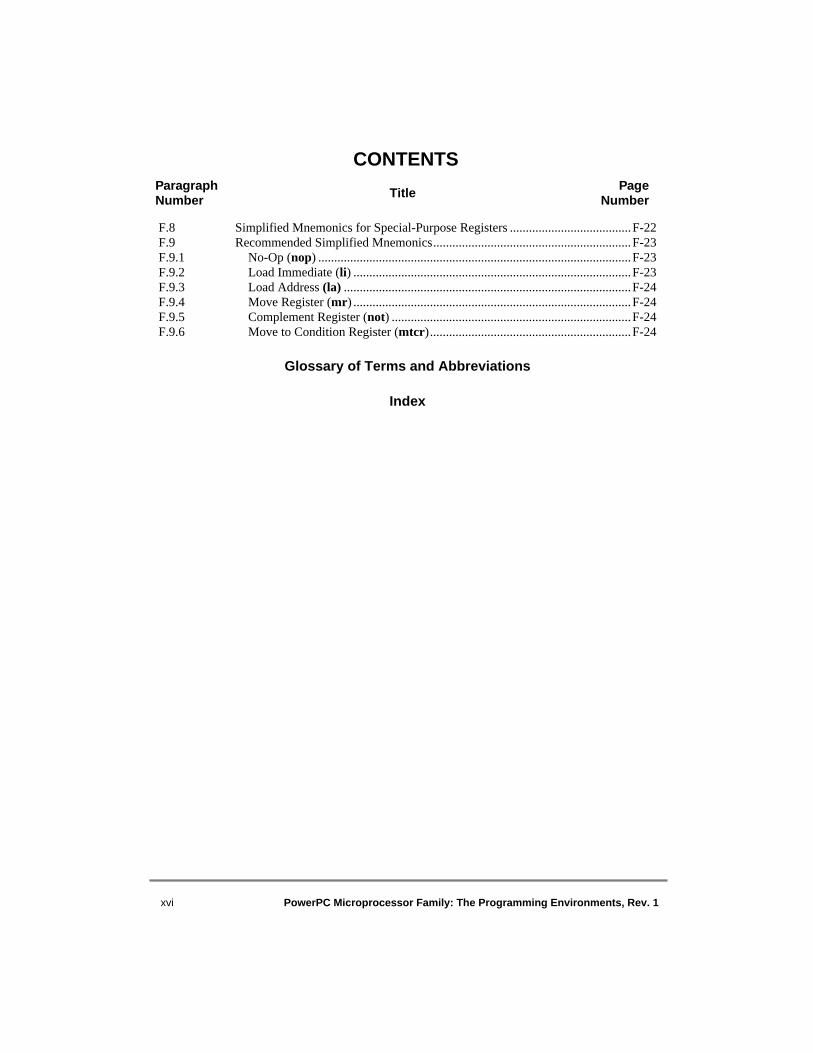
xvi
PowerPC Microprocessor Family: The Programming Environments, Rev. 1
CONTENTS
ParagraphNumber Title Page
Number
F.8 Simplified Mnemonics for Special-Purpose Registers ......................................F-22F.9 Recommended Simplified Mnemonics..............................................................F-23F.9.1 No-Op (
nop
) ..................................................................................................F-23F.9.2 Load Immediate (
li
) .......................................................................................F-23F.9.3 Load Address
(la)
..........................................................................................F-24F.9.4 Move Register (
mr
) .......................................................................................F-24F.9.5 Complement Register (
not
) ...........................................................................F-24F.9.6 Move to Condition Register (
mtcr
)...............................................................F-24
Glossary of Terms and Abbreviations
Index

Illustrations
xvii
ILLUSTRATIONS
FigureNumber Title Page
Number
1-1 Programming Model—PowerPC Registers ......................................................... 1-101-2 Big-Endian Byte and Bit Ordering....................................................................... 1-122-1 UISA Programming Model—User-Level Registers .............................................. 2-22-2 General-Purpose Registers (GPRs) ........................................................................ 2-42-3 Floating-Point Registers (FPRs)............................................................................. 2-52-4 Condition Register (CR)......................................................................................... 2-52-5 Floating-Point Status and Control Register (FPSCR) ............................................ 2-82-6 XER Register........................................................................................................ 2-112-7 Link Register (LR) ............................................................................................... 2-122-8 Count Register (CTR) .......................................................................................... 2-122-9 VEA Programming Model—User-Level Registers Plus Time Base ................... 2-142-10 Time Base (TB).................................................................................................... 2-152-11 OEA Programming Model—All Registers .......................................................... 2-182-12 Machine State Register (MSR)—64-Bit Implementations .................................. 2-212-13 Machine State Register (MSR)—32-Bit Implementations .................................. 2-212-14 Processor Version Register (PVR)....................................................................... 2-242-15 Upper BAT Register—64-Bit Implementations .................................................. 2-252-16 Lower BAT Register—64-Bit Implementations .................................................. 2-252-17 Upper BAT Register—32-Bit Implementations .................................................. 2-252-18 Lower BAT Register—32-Bit Implementations .................................................. 2-262-19 SDR1—64-Bit Implementations .......................................................................... 2-282-20 SDR1—32-Bit Implementations .......................................................................... 2-292-21 Address SpaceRegister (ASR)—64-Bit Implementations Only .......................... 2-302-22 Address Space Register (ASR)—64-Bit Bridge .................................................. 2-312-23 Segment Register Format (T = 0)......................................................................... 2-322-24 Segment Register Format (T = 1)......................................................................... 2-322-25 Data Address Register (DAR).............................................................................. 2-332-26 SPRG0–SPRG3.................................................................................................... 2-342-27 DSISR................................................................................................................... 2-342-28 Machine Status Save/Restore Register 0 (SRR0) ................................................ 2-352-29 Machine Status Save/Restore Register 1 (SRR1) ................................................ 2-352-30 Decrementer Register (DEC) ............................................................................... 2-372-31 Data Address Breakpoint Register (DABR) ........................................................ 2-382-32 External Access Register (EAR) .......................................................................... 2-393-1 C Program Example—Data Structure S................................................................. 3-33-2 Big-Endian Mapping of Structure
S
....................................................................... 3-4

xviii
PowerPC Microprocessor Family: The Programming Environments, Rev. 1
ILLUSTRATIONS
FigureNumber Title Page
Number
3-3 Little-Endian Mapping of Structure
S ....................................................................
3-53-4 Little-Endian Mapping of Structure
S
—Alternate View....................................... 3-63-5 Munged Little-Endian Structure
S
as Seen by the Memory Subsystem ................ 3-73-6 Munged Little-Endian Structure
S
as Seen by Processor ....................................... 3-83-7 True Little-Endian Mapping, Word Stored at Address 05 ..................................... 3-93-8 Word Stored at Little-Endian Address 05 as Seen by the Memory Subsystem... 3-103-9 Floating-Point Single-Precision Format............................................................... 3-163-10 Floating-Point Double-Precision Format ............................................................. 3-163-11 Approximation to Real Numbers ......................................................................... 3-183-12 Format for Normalized Numbers ......................................................................... 3-193-13 Format for Zero Numbers .................................................................................... 3-203-14 Format for Denormalized Numbers ..................................................................... 3-203-15 Format for Positive and Negative Infinities ......................................................... 3-213-16 Format for NaNs................................................................................................... 3-213-17 Representation of Generated QNaN..................................................................... 3-223-18 Single-Precision Representation in an FPR ......................................................... 3-253-19 Relation of Z1 and Z2 .......................................................................................... 3-263-20 Selection of Z1 and Z2 for the Four Rounding Modes ........................................ 3-273-21 Rounding Flags in FPSCR ................................................................................... 3-283-22 Floating-Point Status and Control Register (FPSCR) .......................................... 3-283-23 Initial Flow for Floating-Point Exception Conditions.......................................... 3-363-24 Checking of Remaining Floating-Point Exception Conditions............................ 3-404-1 Register Indirect with Immediate Index Addressing for Integer Loads/Stores.... 4-344-2 Register Indirect with Index Addressing for Integer Loads/Stores...................... 4-354-3 Register Indirect Addressing for Integer Loads/Stores ........................................ 4-364-4 Register Indirect with Immediate Index Addressing for
Floating-Point Loads/Stores ............................................................................ 4-434-5 Register Indirect with Index Addressing for Floating-Point Loads/Stores .......... 4-444-6 Branch Relative Addressing................................................................................. 4-484-7 Branch Conditional Relative Addressing............................................................. 4-494-8 Branch to Absolute Addressing............................................................................ 4-494-9 Branch Conditional to Absolute Addressing........................................................ 4-504-10 Branch Conditional to Link Register Addressing ................................................ 4-514-11 Branch Conditional to Count Register Addressing .............................................. 4-526-1 Machine Status Save/Restore Register 0.............................................................. 6-156-2 Machine Status Save/Restore Register 1.............................................................. 6-156-3 Machine State Register (MSR)—64-Bit Implementation .................................... 6-156-4 Machine State Register (MSR)—32-Bit Implementation .................................... 6-167-1 MMU Conceptual Block Diagram—64-Bit Implementations ............................... 7-97-2 MMU Conceptual Block Diagram—32-Bit Implementations ............................. 7-117-3 Address Translation Types—64-Bit Implementations......................................... 7-147-4 General Flow of Address Translation (Real Addressing Mode and Block) ........ 7-187-5 General Flow of Page and Direct-Store Address Translation .............................. 7-19

Illustrations
xix
ILLUSTRATIONS
FigureNumber Title Page
Number
7-6 Location of Segment Descriptors ......................................................................... 7-217-7 BAT Array Organization—64-Bit Implementations............................................ 7-307-8 BAT Array Hit/Miss Flow—64-Bit Implementations ......................................... 7-327-9 Format of Upper BAT Registers—64-Bit Implementations ................................ 7-347-10 Format of Lower BAT Registers—64-Bit Implementations................................ 7-347-11 Format of Upper BAT Registers—32-Bit Implementations ................................ 7-347-12 Format of Lower BAT Registers—32-Bit Implementations................................ 7-347-13 Memory Protection Violation Flow for Blocks.................................................... 7-397-14 Block Physical Address Generation—64-Bit Implementations........................... 7-407-15 Block Physical Address Generation—32-Bit Implementations........................... 7-417-16 Block Address Translation Flow—64-Bit Implementations................................ 7-427-17 Page Address Translation Overview—64-Bit Implementations .......................... 7-457-18 Page Address Translation Overview—32-Bit Implementations .......................... 7-467-19 STE Format—64-Bit Implementations ................................................................ 7-477-20 Segment Register Format for Page Address Translation—
32-Bit Implementations ................................................................................... 7-497-21 Page Table Entry Format—64-Bit Implementations ........................................... 7-517-22 Page Table Entry Format—32-Bit Implementations ........................................... 7-527-23 Memory Protection Violation Flow for Pages ..................................................... 7-607-24 Page Address Translation Flow for 64-Bit Implementations—TLB Hit ............. 7-627-25 Page Memory Protection Violation Conditions for Page Address Translation ... 7-637-26 Page Table Definitions ......................................................................................... 7-647-27 SDR1 Register Format—64-Bit Implementations ............................................... 7-657-28 SDR1 Register Format—32-Bit Implementations ............................................... 7-667-29 Hashing Functions for Page Tables—64-Bit Implementations............................ 7-717-30 Hashing Functions for Page Tables—32-Bit Implementations............................ 7-727-31 Generation of Addresses for Page Tables—64-Bit Implementations .................. 7-747-32 Generation of Addresses for Page Tables—32-Bit Implementations .................. 7-767-33 Example Page Table Structure—64-Bit Implementations ................................... 7-797-34 Example Page Table Structure—32-Bit Implementations ................................... 7-807-35 Example Primary PTEG Address Generation—64-Bit Implementation ............. 7-827-36 Example Secondary PTEG Address Generation—64-Bit Implementation ......... 7-837-37 Example Primary PTEG Address Generation—32-Bit Implementation ............. 7-857-38 Example Secondary PTEG Address Generation—32-Bit Implementations........ 7-867-39 Page Table Search Flow....................................................................................... 7-907-40 Segment Table Definitions................................................................................... 7-967-41 ASR Format—64-Bit Implementations Only ...................................................... 7-977-42 Hashing Functions for Segment Tables ............................................................... 7-997-43 Generation of Addresses for Segment Table...................................................... 7-1027-44 Example Primary STEG Address Generation .................................................... 7-1047-45 Example Secondary STEG Address Generation ................................................ 7-1057-46 Segment Table Search Flow............................................................................... 7-107

xx
PowerPC Microprocessor Family: The Programming Environments, Rev. 1
ILLUSTRATIONS
FigureNumber Title Page
Number
7-47 Segment Descriptor Format for Direct-Store Segments—64-Bit Implementations ................................................................................. 7-110
7-48 Segment Register Format for Direct-Store Segments—32-Bit Implementations ................................................................................. 7-111
7-49 Direct-Store Segment Translation Flow............................................................. 7-1147-50 GPR Contents for
mfsr
,
mfsrin
,
mtsrd
, and
mtsrdin
...................................... 7-1197-51 GPR Contents for
mtsr
and
mtsrin
................................................................... 7-1218-1 Instruction Description........................................................................................... 8-9D-1 IEEE 64-Bit Execution Model .............................................................................. D-1D-2 Multiply-Add 64-Bit Execution Model................................................................. D-4

Tables
xxi
TABLES
TableNumber Title Page
Number
i Acronyms and Abbreviated Terms...................................................................... xxxivii Terminology Conventions .................................................................................. xxxviiiii Instruction Field Conventions ............................................................................ xxxvii1-1 Optional 64-Bit Bridge Features ........................................................................... 1-191-2 UISA Changes—Rev. 0 to Rev. 0.1 ...................................................................... 1-191-3 UISA Changes—Rev. 0.1 to Rev. 1.0 ................................................................... 1-201-4 VEA Changes—Rev. 0 to Rev. 0.1 ....................................................................... 1-201-5 VEA Changes—Rev. 0.1 to Rev. 1.0 .................................................................... 1-201-6 OEA Changes—Rev. 0 to Rev. 0.1 ....................................................................... 1-211-7 OEA Changes—Rev. 0.1 to Rev. 1.0 .................................................................... 1-212-1 Bit Settings for CR0 Field of CR ............................................................................ 2-62-2 Bit Settings for CR1 Field of CR ............................................................................ 2-62-3 CR
n
Field Bit Settings for Compare Instructions.................................................... 2-72-4 FPSCR Bit Settings ................................................................................................. 2-82-5 Floating-Point Result Flags in FPSCR.................................................................. 2-102-6 XER Bit Definitions .............................................................................................. 2-112-7 BO Operand Encodings......................................................................................... 2-132-8 MSR Bit Settings................................................................................................... 2-212-9 Floating-Point Exception Mode Bits ..................................................................... 2-232-10 State of MSR at Power Up .................................................................................... 2-232-11 BAT Registers—Field and Bit Descriptions ......................................................... 2-262-12 BAT Area Lengths ................................................................................................ 2-272-13 SDR1 Bit Settings—64-Bit Implementations ....................................................... 2-282-14 SDR1 Bit Settings—32-Bit Implementations ....................................................... 2-292-15 ASR Bit Settings.................................................................................................... 2-302-16 ASR Bit Settings—64-Bit Bridge ......................................................................... 2-312-17 Segment Register Bit Settings (T = 0)................................................................... 2-322-18 Segment Register Bit Settings (T = 1)................................................................... 2-322-19 Conventional Uses of SPRG0–SPRG3 ................................................................. 2-342-20 DABR—Bit Settings ............................................................................................. 2-382-21 External Access Register (EAR) Bit Settings ....................................................... 2-402-22 Data Access Synchronization ................................................................................ 2-412-23 Instruction Access Synchronization ...................................................................... 2-423-1 Memory Operand Alignment .................................................................................. 3-23-2 EA Modifications .................................................................................................... 3-73-3 Performance Effects of Memory Operand Placement, Big-Endian Mode ............ 3-13

xxii
PowerPC Microprocessor Family: The Programming Environments, Rev. 1
TABLESTableNumber Title Page
Number
3-4 Performance Effects of Memory Operand Placement, Little-Endian Mode ......... 3-143-5 IEEE Floating-Point Fields.................................................................................... 3-173-6 Biased Exponent Format ....................................................................................... 3-173-7 Recognized Floating-Point Numbers .................................................................... 3-183-8 FPSCR Bit Settings—RN Field............................................................................. 3-263-9 FPSCR Bit Settings ............................................................................................... 3-293-10 Floating-Point Result Flags — FPSCR[FPRF] ..................................................... 3-313-11 MSR[FE0] and MSR[FE1] Bit Settings for FP Exceptions .................................. 3-343-12 Additional Actions Performed for Invalid FP Operations..................................... 3-383-13 Additional Actions Performed for Zero Divide..................................................... 3-393-14 Additional Actions Performed for Overflow Exception Condition ...................... 3-413-15 Target Result for Overflow Exception Disabled Case .......................................... 3-423-16 Actions Performed for Underflow Conditions ...................................................... 3-434-1 Integer Arithmetic Instructions.............................................................................. 4-124-2 Integer Compare Instructions ................................................................................ 4-184-3 Integer Logical Instructions................................................................................... 4-194-4 Integer Rotate Instructions .................................................................................... 4-224-5 Integer Shift Instructions ....................................................................................... 4-244-6 Floating-Point Arithmetic Instructions.................................................................. 4-264-7 Floating-Point Multiply-Add Instructions............................................................. 4-284-8 Floating-Point Rounding and Conversion Instructions ......................................... 4-304-9 CR Bit Settings ...................................................................................................... 4-314-10 Floating-Point Compare Instructions .................................................................... 4-314-11 Floating-Point Status and Control Register Instructions ....................................... 4-324-12 Floating-Point Move Instructions.......................................................................... 4-334-13 Integer Load Instructions....................................................................................... 4-374-14 Integer Store Instructions ...................................................................................... 4-394-15 Integer Load and Store with Byte-Reverse Instructions........................................ 4-404-16 Integer Load and Store Multiple Instructions........................................................ 4-414-17 Integer Load and Store String Instructions............................................................ 4-424-18 Floating-Point Load Instructions........................................................................... 4-444-19 Floating-Point Store Instructions........................................................................... 4-464-20 BO Operand Encodings......................................................................................... 4-524-21 Branch Instructions................................................................................................ 4-554-22 Condition Register Logical Instructions................................................................ 4-564-23 Trap Instructions.................................................................................................... 4-574-24 System Linkage Instruction—UISA...................................................................... 4-574-25 Move to/from Condition Register Instructions...................................................... 4-584-26 Move to/from Special-Purpose Register Instructions (UISA)............................... 4-584-27 Memory Synchronization Instructions—UISA..................................................... 4-604-28 Move from Time Base Instruction ........................................................................ 4-624-29 User-Level TBR Encodings (VEA)....................................................................... 4-624-30 Supervisor-Level TBR Encodings (VEA)............................................................. 4-63

Tables xxiii
TABLESTableNumber Title Page
Number
4-31 Memory Synchronization Instructions—VEA ...................................................... 4-644-32 User-Level Cache Instructions .............................................................................. 4-654-33 External Control Instructions ................................................................................ 4-684-34 System Linkage Instructions—OEA ..................................................................... 4-694-35 Move to/from Machine State Register Instructions............................................... 4-714-36 Move to/from Special-Purpose Register Instructions (OEA)................................ 4-714-37 Cache Management Supervisor-Level Instruction ................................................ 4-734-38 Segment Register Manipulation Instructions ........................................................ 4-744-39 Translation Lookaside Buffer Management Instructions ...................................... 4-765-1 Combinations of W, I, and M Bits ........................................................................ 5-156-1 PowerPC Exception Classifications ........................................................................ 6-36-2 Exceptions and Conditions—Overview .................................................................. 6-46-3 IEEE Floating-Point Program Exception Mode Bits............................................. 6-106-4 Exception Priorities ............................................................................................... 6-126-5 MSR Bit Settings................................................................................................... 6-166-6 MSR Setting Due to Exception ............................................................................. 6-226-7 System Reset Exception—Register Settings ......................................................... 6-236-8 Machine Check Exception—Register Settings ..................................................... 6-256-9 DSI Exception—Register Settings ........................................................................ 6-276-10 ISI Exception—Register Settings.......................................................................... 6-296-11 External Interrupt—Register Settings ................................................................... 6-306-12 Alignment Exception—Register Settings.............................................................. 6-316-13 DSISR(15–21) Settings to Determine Misaligned Instruction.............................. 6-346-14 Program Exception—Register Settings................................................................. 6-376-15 Floating-Point Unavailable Exception—Register Settings ................................... 6-386-16 Decrementer Exception—Register Settings .......................................................... 6-396-17 System Call Exception—Register Settings ........................................................... 6-406-18 Trace Exception—Register Settings...................................................................... 6-416-19 Floating-Point Assist Exception—Register Settings............................................. 6-427-1 MMU Features Summary ........................................................................................ 7-37-2 Predefined Physical Memory Locations.................................................................. 7-77-3 Value of Base for Predefined Memory Use ............................................................ 7-77-4 Access Protection Options for Pages..................................................................... 7-157-5 Translation Exception Conditions ......................................................................... 7-237-6 Other MMU Exception Conditions ....................................................................... 7-247-7 Instruction Summary—Control MMU.................................................................. 7-267-8 MMU Registers ..................................................................................................... 7-277-9 BAT Registers—Field and Bit Descriptions for 64-Bit Implementations ............ 7-357-10 Upper BAT Register Block Size Mask Encodings................................................ 7-367-11 Access Protection Control for Blocks ................................................................... 7-377-12 Access Protection Summary for BAT Array......................................................... 7-387-13 Segment Descriptor Types .................................................................................... 7-437-14 STE Bit Definitions for Page Address Translation—64-Bit Implementations ..... 7-48

xxiv PowerPC Microprocessor Family: The Programming Environments, Rev. 1
TABLESTableNumber Title Page
Number
7-15 Segment Register Bit Definition for Page Address Translation—32-Bit Implementations ................................................................................... 7-49
7-16 Segment Register Instructions—32-Bit Implementations..................................... 7-507-17 PTE Bit Definitions—64-Bit Implementations ..................................................... 7-527-18 PTE Bit Definitions—32-Bit Implementations ..................................................... 7-537-19 Table Search Operations to Update History Bits .................................................. 7-547-20 Model for Guaranteed R and C Bit Settings.......................................................... 7-567-21 Access Protection Control with Key ..................................................................... 7-587-22 . Exception Conditions for Key and PP Combinations ........................................ 7-597-23 Access Protection Encoding of PP Bits for Ks = 0 and Kp = 1............................. 7-597-24 SDR1 Register Bit Settings—64-Bit Implementations ......................................... 7-657-25 SDR1 Register Bit Settings—32-Bit Implementations ......................................... 7-677-26 Minimum Recommended Page Table Sizes—64-Bit Implementations................ 7-687-27 Minimum Recommended Page Table Sizes—32-Bit Implementations................ 7-697-28 Segment Descriptor Bit Definitions for Direct-Store Segments—
64-Bit Implementations ................................................................................. 7-1117-29 Segment Register Bit Definitions for Direct-Store Segments ............................. 7-1117-30 Contents of rD after Executing mfsr................................................................... 7-1187-31 SLB Entry Following mfsrin .............................................................................. 7-1197-32 SLB Entry Following mtsr ................................................................................. 7-1207-33 SLB Entry Following mtsrin .............................................................................. 7-1217-34 SLB Entry Following mtsrd ............................................................................... 7-1237-35 SLB Entry Following mtsrdin ............................................................................ 7-1248-1 Split-Field Notation and Conventions ..................................................................... 8-28-2 Instruction Syntax Conventions .............................................................................. 8-28-3 Notation and Conventions ....................................................................................... 8-48-4 Instruction Field Conventions ................................................................................. 8-78-5 Precedence Rules..................................................................................................... 8-88-6 BO Operand Encodings......................................................................................... 8-248-7 BO Operand Encodings......................................................................................... 8-268-8 BO Operand Encodings......................................................................................... 8-288-9 PowerPC UISA SPR Encodings for mfspr......................................................... 8-1558-10 PowerPC OEA SPR Encodings for mfspr .......................................................... 8-1568-11 GPR Content Format Following mfsr................................................................. 8-1588-12 GPR Content Format Following mfsrin ............................................................. 8-1608-13 TBR Encodings for mftb..................................................................................... 8-1628-14 PowerPC UISA SPR Encodings for mtspr......................................................... 8-1728-15 PowerPC OEA SPR Encodings for mtspr .......................................................... 8-1738-16 SLB Entry Following mtsr ................................................................................. 8-1758-17 SLB Entry Following mtsrd ............................................................................... 8-1778-18 SLB Entry following mtsrdin............................................................................. 8-1788-19 SLB Entry Following mtsrin .............................................................................. 8-180
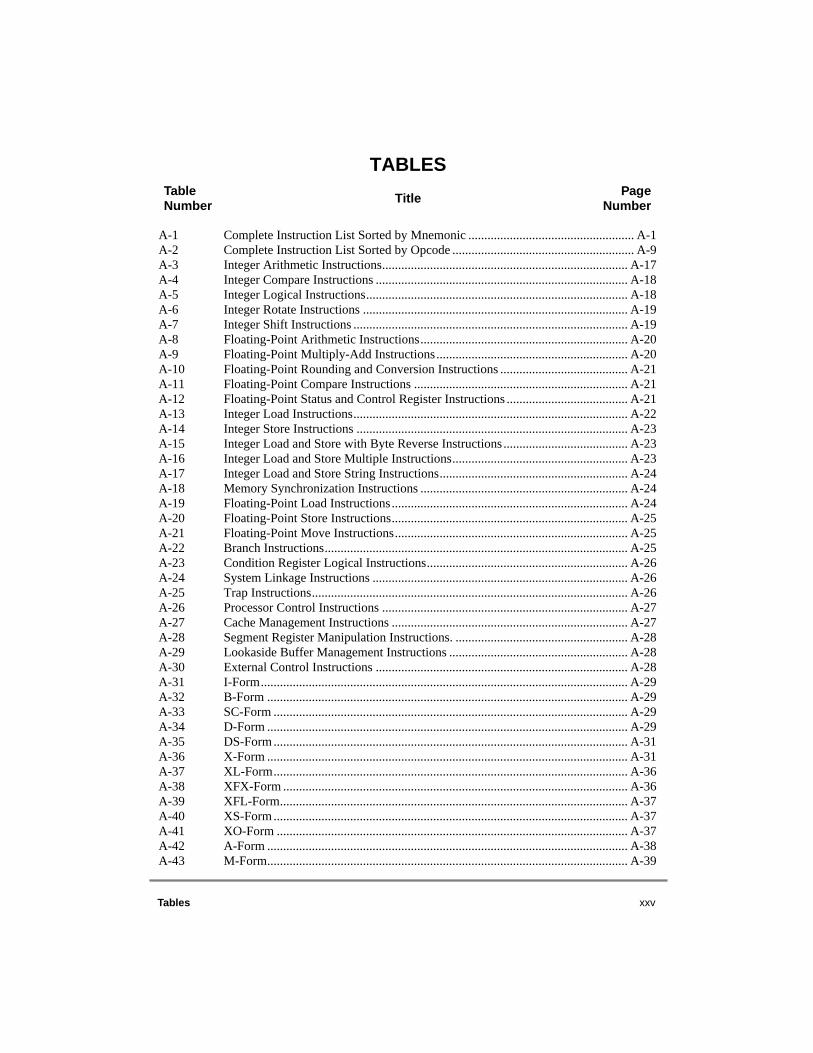
Tables xxv
TABLESTableNumber Title Page
Number
A-1 Complete Instruction List Sorted by Mnemonic .................................................... A-1A-2 Complete Instruction List Sorted by Opcode ......................................................... A-9A-3 Integer Arithmetic Instructions............................................................................. A-17A-4 Integer Compare Instructions ............................................................................... A-18A-5 Integer Logical Instructions.................................................................................. A-18A-6 Integer Rotate Instructions ................................................................................... A-19A-7 Integer Shift Instructions ...................................................................................... A-19A-8 Floating-Point Arithmetic Instructions................................................................. A-20A-9 Floating-Point Multiply-Add Instructions............................................................ A-20A-10 Floating-Point Rounding and Conversion Instructions ........................................ A-21A-11 Floating-Point Compare Instructions ................................................................... A-21A-12 Floating-Point Status and Control Register Instructions ...................................... A-21A-13 Integer Load Instructions...................................................................................... A-22A-14 Integer Store Instructions ..................................................................................... A-23A-15 Integer Load and Store with Byte Reverse Instructions ....................................... A-23A-16 Integer Load and Store Multiple Instructions....................................................... A-23A-17 Integer Load and Store String Instructions........................................................... A-24A-18 Memory Synchronization Instructions ................................................................. A-24A-19 Floating-Point Load Instructions.......................................................................... A-24A-20 Floating-Point Store Instructions.......................................................................... A-25A-21 Floating-Point Move Instructions......................................................................... A-25A-22 Branch Instructions............................................................................................... A-25A-23 Condition Register Logical Instructions............................................................... A-26A-24 System Linkage Instructions ................................................................................ A-26A-25 Trap Instructions................................................................................................... A-26A-26 Processor Control Instructions ............................................................................. A-27A-27 Cache Management Instructions .......................................................................... A-27A-28 Segment Register Manipulation Instructions. ...................................................... A-28A-29 Lookaside Buffer Management Instructions ........................................................ A-28A-30 External Control Instructions ............................................................................... A-28A-31 I-Form................................................................................................................... A-29A-32 B-Form ................................................................................................................. A-29A-33 SC-Form ............................................................................................................... A-29A-34 D-Form ................................................................................................................. A-29A-35 DS-Form............................................................................................................... A-31A-36 X-Form ................................................................................................................. A-31A-37 XL-Form............................................................................................................... A-36A-38 XFX-Form ............................................................................................................ A-36A-39 XFL-Form............................................................................................................. A-37A-40 XS-Form............................................................................................................... A-37A-41 XO-Form .............................................................................................................. A-37A-42 A-Form ................................................................................................................. A-38A-43 M-Form................................................................................................................. A-39

xxvi PowerPC Microprocessor Family: The Programming Environments, Rev. 1
TABLESTableNumber Title Page
Number
A-44 MD-Form.............................................................................................................. A-39A-45 MDS-Form ........................................................................................................... A-40A-46 PowerPC Instruction Set Legend.......................................................................... A-41B-1 Condition Register Settings.....................................................................................B-2B-2 Deleted POWER Instructions..................................................................................B-9B-3 POWER Instructions Implemented in PowerPC Architecture ..............................B-11D-1 Interpretation of G, R, and X Bits .......................................................................... D-2D-2 Location of the Guard, Round, and Sticky Bits—IEEE Execution Model ............ D-3D-3 Location of the Guard, Round, and Sticky Bits—
Multiply-Add Execution Model ....................................................................... D-4F-1 Condition Register Bit and Identification Symbol Descriptions.............................F-1F-2 Simplified Mnemonics for Double-Word Compare Instructions ............................F-3F-3 Simplified Mnemonics for Word Compare Instructions .........................................F-4F-4 Double-Word Rotate and Shift Instructions ............................................................F-5F-5 Word Rotate and Shift Instructions .........................................................................F-6F-6 Simplified Branch Mnemonics................................................................................F-8F-7 Simplified Branch Mnemonics for bc and bca Instructions
without Link Register Update ...........................................................................F-9F-8 Simplified Branch Mnemonics for bclr and bcclr Instructions
without Link Register Update .........................................................................F-10F-9 Simplified Branch Mnemonics for bcl and bcla Instructions
with Link Register Update...............................................................................F-11F-10 Simplified Branch Mnemonics for bclrl and bcctrl Instructions
with Link Register Update...............................................................................F-12F-11 Standard Coding for Branch Conditions ...............................................................F-13F-12 Simplified Branch Mnemonics with Comparison Conditions...............................F-14F-13 Simplified Branch Mnemonics for bc and bca Instructions without
Comparison Conditions and Link Register Updating .....................................F-15F-14 Simplified Branch Mnemonics for bclr and bcctr Instructions without
Comparison Conditions and Link Register Updating .....................................F-16F-15 Simplified Branch Mnemonics for bcl and bcla Instructions with
Comparison Conditions and Link Register Update.........................................F-17F-16 Simplified Branch Mnemonics for bclrl and bcctl Instructions with
Comparison Conditions and Link Register Update.........................................F-18F-17 Condition Register Logical Mnemonics................................................................F-19F-18 Standard Codes for Trap Instructions....................................................................F-20F-19 Trap Mnemonics....................................................................................................F-21F-20 TO Operand Bit Encoding.....................................................................................F-22F-21 Simplified Mnemonics for SPRs ...........................................................................F-22

About This Book xxvii
About This BookThe primary objective of this manual is to help programmers provide software that iscompatible across the family of PowerPC™ processors. Because the PowerPC architectureis designed to be flexible to support a broad range of processors, this book provides ageneral description of features that are common to PowerPC processors and indicates thosefeatures that are optional or that may be implemented differently in the design of eachprocessor.
This revision of this book describes both the 64- and the 32-bit portions of the PowerPCarchitecture from the perspective of the 64-bit architecture. The information in this manualthat pertains only to the 32-bit architecture is presented in PowerPC MicroprocessorFamily: The Programming Environments for 32-Bit Microprocessors. Both books reflectchanges to the PowerPC architecture made subsequent to the publication of PowerPCMicroprocessor Family: The Programming Environments, Rev. 0 and Rev. 0.1.
To locate any published errata or updates for this document, refer to the world-wide web athttp://www.mot.com/powerpc/ or at http://www.chips.ibm.com/products/ppc.
For designers working with a specific processor, this book should be used in conjunctionwith the user’s manual for that processor. For information regarding variances between aprocessor implementation and the version of the PowerPC architecture reflected in thisdocument, see the reference to Implementation Variances Relative to Rev. 1 of TheProgramming Environments Manual described in “PowerPC Documentation,” on Pagexxxi.
This document distinguishes between the three levels, or programming environments, ofthe PowerPC architecture, which are as follows:
• PowerPC user instruction set architecture (UISA)—The UISA defines the level of the architecture to which user-level software should conform. The UISA defines the base user-level instruction set, user-level registers, data types, memory conventions, and the memory and programming models seen by application programmers.
• PowerPC virtual environment architecture (VEA)—The VEA, which is the smallest component of the PowerPC architecture, defines additional user-level functionality that falls outside typical user-level software requirements. The VEA describes the memory model for an environment in which multiple processors or other devices can access external memory, and defines aspects of the cache model and cache control instructions from a user-level perspective. The resources defined by the VEA are
xxviii PowerPC Microprocessor Family: The Programming Environments, Rev. 1
particularly useful for optimizing memory accesses and for managing resources in an environment in which other processors and other devices can access external memory.
Implementations that conform to the PowerPC VEA also adhere to the UISA, but may not necessarily adhere to the OEA.
• PowerPC operating environment architecture (OEA)—The OEA defines supervisor-level resources typically required by an operating system. The OEA defines the PowerPC memory management model, supervisor-level registers, and the exception model.
Implementations that conform to the PowerPC OEA also conform to the PowerPC UISA and VEA.
It is important to note that some resources are defined more generally at one level in thearchitecture and more specifically at another. For example, conditions that can cause afloating-point exception are defined by the UISA, while the exception mechanism itself isdefined by the OEA.
Because it is important to distinguish between the levels of the architecture in order toensure compatibility across multiple platforms, those distinctions are shown clearlythroughout this book. The level of the architecture to which text refers is indicated in theouter margin, using the conventions shown in “Conventions,” on Page xxxiii.
This book does not attempt to replace the PowerPC architecture specification, whichdefines the architecture from the perspective of the three programming environments andwhich remains the defining document for the PowerPC architecture. This book reflectschanges made to the architecture before August 6, 1996. These changes are described inSection 1.3, “Changes in This Revision of The Programming Environments Manual.” Forinformation about the architecture specification, see “General Information,” on Page xxx.
For ease in reference, this book and the processor user’s manuals have arranged thearchitecture information into topics that build upon one another, beginning with adescription and complete summary of registers and instructions (for all three environments)and progressing to more specialized topics such as the cache, exception, and memorymanagement models. As such, chapters may include information from multiple levels of thearchitecture; for example, the discussion of the cache model uses information from both theVEA and the OEA.
It is beyond the scope of this manual to describe individual PowerPC processors. It must bekept in mind that each PowerPC processor is unique in its implementation of the PowerPCarchitecture.
TEMPORARY 64-BIT BRIDGE
The OEA also defines optional features to simplify the migration of 32-bit operating systems to 64-bit implementations.

About This Book xxix
The information in this book is subject to change without notice, as described in thedisclaimers on the title page of this book. As with any technical documentation, it is thereaders’ responsibility to be sure they are using the most recent version of thedocumentation. For more information, contact your sales representative.
AudienceThis manual is intended for system software and hardware developers and applicationprogrammers who want to develop products for the PowerPC processors in general. It isassumed that the reader understands operating systems, microprocessor system design, andthe basic principles of RISC processing.
This revision of this book describes both the 64- and the 32-bit portions of the PowerPCarchitecture, primarily from the perspective of the 64-bit architectural definition. Theinformation in this manual that pertains only to the 32-bit architecture is also presentedseparately in PowerPC Microprocessor Family: The Programming Environments for 32-Bit Microprocessors.
OrganizationFollowing is a summary and a brief description of the major sections of this manual:
• Chapter 1, “Overview,” is useful for those who want a general understanding of the features and functions of the PowerPC architecture. This chapter describes the flexible nature of the PowerPC architecture definition and provides an overview of how the PowerPC architecture defines the register set, operand conventions, addressing modes, instruction set, cache model, exception model, and memory management model.
• Chapter 2, “PowerPC Register Set,” is useful for software engineers who need to understand the PowerPC programming model for the three programming environments and the functionality of the PowerPC registers.
• Chapter 3, “Operand Conventions,” describes PowerPC conventions for storing data in memory, including information regarding alignment, single- and double-precision floating-point conventions, and big- and little-endian byte ordering.
• Chapter 4, “Addressing Modes and Instruction Set Summary,” provides an overview of the PowerPC addressing modes and a description of the PowerPC instructions. Instructions are organized by function.
• Chapter 5, “Cache Model and Memory Coherency,” provides a discussion of the cache and memory model defined by the VEA and aspects of the cache model that are defined by the OEA.
• Chapter 6, “Exceptions,” describes the exception model defined in the OEA.
• Chapter 7, “Memory Management,” provides descriptions of the PowerPC address translation and memory protection mechanism as defined by the OEA.

xxx PowerPC Microprocessor Family: The Programming Environments, Rev. 1
• Chapter 8, “Instruction Set,” functions as a handbook for the PowerPC instruction set. Instructions are sorted by mnemonic. Each instruction description includes the instruction formats and an individualized legend that provides such information as the level(s) of the PowerPC architecture in which the instruction may be found and the privilege level of the instruction.
• Appendix A, “PowerPC Instruction Set Listings,” lists all the PowerPC instructions. Instructions are grouped according to mnemonic, opcode, function, and form.
• Appendix B, “POWER Architecture Cross Reference,” identifies the differences that must be managed in migration from the POWER architecture to the PowerPC architecture.
• Appendix C, “Multiple-Precision Shifts,” describes how multiple-precision shift operations can be programmed as defined by the UISA.
• Appendix D, “Floating-Point Models,” gives examples of how the floating-point conversion instructions can be used to perform various conversions as described in the UISA.
• Appendix E, “Synchronization Programming Examples,” gives examples showing how synchronization instructions can be used to emulate various synchronization primitives and how to provide more complex forms of synchronization.
• Appendix F, “Simplified Mnemonics,” provides a set of simplified mnemonic examples and symbols.
• This manual also includes a glossary and an index.
Suggested ReadingThis section lists additional reading that provides background for the information in thismanual as well as general information about the PowerPC architecture.
General InformationThe following documentation provides useful information about the PowerPC architectureand computer architecture in general:
• The following books are available from the Morgan-Kaufmann Publishers, 340 Pine Street, Sixth Floor, San Francisco, CA 94104; Tel. (800) 745-7323 (U.S.A.), (415) 392-2665 (International); internet address: [email protected].
— The PowerPC Architecture: A Specification for a New Family of RISC Processors, Second Edition, by International Business Machines, Inc.
Updates to the architecture specification are accessible via the world-wide web at http://www.austin.ibm.com/tech/ppc-chg.html.
— PowerPC Microprocessor Common Hardware Reference Platform: A System Architecture, by Apple Computer, Inc., International Business Machines, Inc., and Motorola, Inc.

About This Book xxxi
— Macintosh Technology in the Common Hardware Reference Platform, by Apple Computer, Inc.
— Computer Architecture: A Quantitative Approach, Second Edition, by John L. Hennessy and David A. Patterson,
• Inside Macintosh: PowerPC System Software, Addison-Wesley Publishing Company, One Jacob Way, Reading, MA, 01867; Tel. (800) 282-2732 (U.S.A.), (800) 637-0029 (Canada), (716) 871-6555 (International).
• PowerPC Programming for Intel Programmers, by Kip McClanahan; IDG Books Worldwide, Inc., 919 East Hillsdale Boulevard, Suite 400, Foster City, CA, 94404; Tel. (800) 434-3422 (U.S.A.), (415) 655-3022 (International).
PowerPC DocumentationThe PowerPC documentation is organized in the following types of documents:
• User’s manuals—These books provide details about individual PowerPC implementations and are intended to be used in conjunction with The Programming Environments Manual. These include the following:
— PowerPC 601™ RISC Microprocessor User’s Manual: MPC601UM/AD (Motorola order #) and 52G7484/(MPR601UMU-02) (IBM order #)
— PowerPC 602™ RISC Microprocessor User’s Manual: MPC602UM/AD (Motorola order #) and MPR602UM-01 (IBM order #)
— PowerPC 603e™ RISC Microprocessor User’s Manual with Supplement for PowerPC 603 Microprocessor: MPC603EUM/AD (Motorola order #) and MPR603EUM-01 (IBM order #)
— PowerPC 604™ RISC Microprocessor User’s Manual:MPC604UM/AD (Motorola order #) and MPR604UMU-01 (IBM order #)
• Implementation Variances Relative to Rev. 1 of The Programming Environments Manual is available via the world-wide web at http://www.mot.com/powerpc/ or at http://www.chips.ibm.com/products/ppc.
• Addenda/errata to user’s manuals—Because some processors have follow-on parts an addendum is provided that describes the additional features and changes to functionality of the follow-on part. These addenda are intended for use with the corresponding user’s manuals. These include the following:
— Addendum to PowerPC 603e RISC Microprocessor User’s Manual: PowerPC 603e Microprocessor Supplement and User’s Manual Errata: MPC603EUMAD/AD (Motorola order #) and SA14-2034-00 (IBM order #)
— Addendum to PowerPC 604 RISC Microprocessor User’s Manual: PowerPC 604e™ Microprocessor Supplement and User’s Manual Errata: MPC604UMAD/AD (Motorola order #) and SA14-2056-01 (IBM order #)

xxxii PowerPC Microprocessor Family: The Programming Environments, Rev. 1
• Hardware specifications—Hardware specifications provide specific data regarding bus timing, signal behavior, and AC, DC, and thermal characteristics, as well as other design considerations for each PowerPC implementation. These include the following:
— PowerPC 601 RISC Microprocessor Hardware Specifications: MPC601EC/D (Motorola order #) and MPR601HSU-03 (IBM order #)
— PowerPC 602 RISC Microprocessor Hardware Specifications: MPC602EC/D (Motorola order #) and SC229897-00 (IBM order #)
— PowerPC 603 RISC Microprocessor Hardware Specifications:MPC603EC/D (Motorola order #) and MPR603HSU-03 (IBM order #)
— PowerPC 603e RISC Microprocessor Family: PID6-603e Hardware Specifications: MPC603EEC/D (Motorola order #) and G522-0268-00 (IBM order #)
— PowerPC 603e RISC Microprocessor Family: PID7V-603e Hardware Specifications: MPC603E7VEC/D (Motorola order #) and G522-0267-00 (IBM order #)
— PowerPC 604 RISC Microprocessor Hardware Specifications:MPC604EC/D (Motorola order #) and MPR604HSU-02 (IBM order #)
— PowerPC 604e RISC Microprocessor Family: PID9V-604e Hardware Specifications: MPC604E9VEC/D (Motorola order #) and SA14-2054-00 (IBM order #)
• Technical Summaries—Each PowerPC implementation has a technical summary that provides an overview of its features. This document is roughly the equivalent to the overview (Chapter 1) of an implementation’s user’s manual. Technical summaries are available for the 601, 602, 603, 603e, 604, and 604e as well as the following:
— PowerPC 620™ RISC Microprocessor Technical Summary: MPC620/D (Motorola order #) and SA14-2069-01 (IBM order #)
• PowerPC Microprocessor Family: The Bus Interface for 32-Bit Microprocessors: MPCBUSIF/AD (Motorola order #) and G522-0291-00 (IBM order #) provides a detailed functional description of the 60x bus interface, as implemented on the 601, 603, and 604 family of PowerPC microprocessors. This document is intended to help system and chipset developers by providing a centralized reference source to identify the bus interface presented by the 60x family of PowerPC microprocessors.
• PowerPC Microprocessor Family: The Programmer’s Reference Guide: MPCPRG/D (Motorola order #) and MPRPPCPRG-01 (IBM order #) is a concise reference that includes the register summary, memory control model, exception vectors, and the PowerPC instruction set.

About This Book xxxiii
• PowerPC Microprocessor Family: The Programmer’s Pocket Reference Guide: MPCPRGREF/D (Motorola order #) and SA14-2093-00 (IBM order #): This foldout card provides an overview of the PowerPC registers, instructions, and exceptions for 32-bit implementations.
• Application notes—These short documents contain useful information about specific design issues useful to programmers and engineers working with PowerPC processors.
• Documentation for support chips—These include the following:
— MPC105 PCI Bridge/Memory Controller User’s Manual:MPC105UM/AD (Motorola order #)
— MPC106 PCI Bridge/Memory Controller User’s Manual:MPC106UM/AD (Motorola order #)
Additional literature on PowerPC implementations is being released as new processorsbecome available. For a current list of PowerPC documentation, refer to the world-wideweb at http://www.mot.com/powerpc/ or at http://www.chips.ibm.com/products/ppc.
ConventionsThis document uses the following notational conventions:
mnemonics Instruction mnemonics are shown in lowercase bold.
italics Italics indicate variable command parameters, for example, bcctrx.Book titles in text are set in italics.
0x0 Prefix to denote hexadecimal number
0b0 Prefix to denote binary number
rA, rB Instruction syntax used to identify a source GPR
rD Instruction syntax used to identify a destination GPR
frA, frB, frC Instruction syntax used to identify a source FPR
frD Instruction syntax used to identify a destination FPR
REG[FIELD] Abbreviations or acronyms for registers are shown in uppercase text. Specific bits, fields, or ranges appear in brackets. For example, MSR[LE] refers to the little-endian mode enable bit in the machine state register.
x In certain contexts, such as a signal encoding, this indicates a don’t care.
n Used to express an undefined numerical value
¬ NOT logical operator
& AND logical operator
| OR logical operator

xxxiv PowerPC Microprocessor Family: The Programming Environments, Rev. 1
This symbol identifies text that is relevant with respect to the PowerPC user instruction set architecture (UISA). This symbol is used both for information that can be found in the UISA specification as well as for explanatory information related to that programming environment.
This symbol identifies text that is relevant with respect to the PowerPC virtual environment architecture (VEA). This symbol is used both for information that can be found in the VEA specification as well as for explanatory information related to that programming environment.
This symbol identifies text that is relevant with respect to the PowerPC operating environment architecture (OEA). This symbol is used both for information that can be found in the OEA specification as well as for explanatory information related to that programming environment.
Indicates reserved bits or bit fields in a register. Although these bits may be written to as either ones or zeroes, they are always read as zeros.
Additional conventions used with instruction encodings are described in Table 8-2 on page8-2. Conventions used for pseudocode examples are described in Table 8-3 on page 8-4.
Acronyms and AbbreviationsTable i contains acronyms and abbreviations that are used in this document. Note that themeanings for some acronyms (such as SDR1 and XER) are historical, and the words forwhich an acronym stands may not be intuitively obvious.
TEMPORARY 64-BIT BRIDGE
Text that pertains to the optional 64-bit bridge defined by the OEA is presented with a grayed background, as shown here.
Table i. Acronyms and Abbreviated Terms
Term Meaning
ALU Arithmetic logic unit
ASR Address space register
BAT Block address translation
BIST Built-in self test
BPU Branch processing unit
BUID Bus unit ID
CR Condition register
U
V
O
0 0 0 0
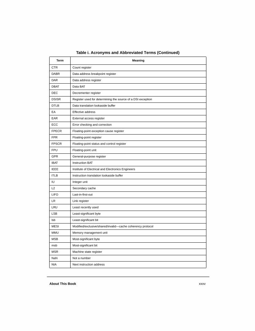
About This Book xxxv
CTR Count register
DABR Data address breakpoint register
DAR Data address register
DBAT Data BAT
DEC Decrementer register
DSISR Register used for determining the source of a DSI exception
DTLB Data translation lookaside buffer
EA Effective address
EAR External access register
ECC Error checking and correction
FPECR Floating-point exception cause register
FPR Floating-point register
FPSCR Floating-point status and control register
FPU Floating-point unit
GPR General-purpose register
IBAT Instruction BAT
IEEE Institute of Electrical and Electronics Engineers
ITLB Instruction translation lookaside buffer
IU Integer unit
L2 Secondary cache
LIFO Last-in-first-out
LR Link register
LRU Least recently used
LSB Least-significant byte
lsb Least-significant bit
MESI Modified/exclusive/shared/invalid—cache coherency protocol
MMU Memory management unit
MSB Most-significant byte
msb Most-significant bit
MSR Machine state register
NaN Not a number
NIA Next instruction address
Table i. Acronyms and Abbreviated Terms (Continued)
Term Meaning

xxxvi PowerPC Microprocessor Family: The Programming Environments, Rev. 1
No-op No operation
OEA Operating environment architecture
PIR Processor identification register
PTE Page table entry
PTEG Page table entry group
PVR Processor version register
RISC Reduced instruction set computing
RTL Register transfer language
RWITM Read with intent to modify
SDR1 Register that specifies the page table base address for virtual-to-physical address translation
SIMM Signed immediate value
SLB Segment lookaside buffer
SPR Special-purpose register
SPRGn Registers available for general purposes
SR Segment register
SRR0 Machine status save/restore register 0
SRR1 Machine status save/restore register 1
STE Segment table entry
TB Time base register
TLB Translation lookaside buffer
UIMM Unsigned immediate value
UISA User instruction set architecture
VA Virtual address
VEA Virtual environment architecture
XATC Extended address transfer code
XER Register used primarily for indicating conditions such as carries and overflows for integer operations
Table i. Acronyms and Abbreviated Terms (Continued)
Term Meaning

About This Book xxxvii
Terminology ConventionsTable ii lists certain terms used in this manual that differ from the architecture terminologyconventions.
Table iii describes instruction field notation conventions used in this manual.
Table ii. Terminology Conventions
The Architecture Specification This Manual
Data storage interrupt (DSI) DSI exception
Extended mnemonics Simplified mnemonics
Instruction storage interrupt (ISI) ISI exception
Interrupt Exception
Privileged mode (or privileged state) Supervisor-level privilege
Problem mode (or problem state) User-level privilege
Real address Physical address
Relocation Translation
Storage (locations) Memory
Storage (the act of) Access
Table iii. Instruction Field Conventions
The Architecture Specification Equivalent to:
BA, BB, BT crbA, crbB, crbD (respectively)
BF, BFA crfD, crfS (respectively)
D d
DS ds
FLM FM
FRA, FRB, FRC, FRT, FRS frA, frB, frC, frD, frS (respectively)
FXM CRM
RA, RB, RT, RS rA, rB, rD, rS (respectively)
SI SIMM
U IMM
UI UIMM
/, //, /// 0...0 (shaded)

xxxviii PowerPC Microprocessor Family: The Programming Environments, Rev. 1

Chapter 1. Overview 1-1
Chapter 1 Overview1010
The PowerPC™ architecture provides a software model that ensures software compatibilityamong implementations of the PowerPC family of microprocessors. In this document, andin other PowerPC documentation as well, the term ‘implementation’ refers to a hardwaredevice (typically a microprocessor) that complies with the specifications defined by thearchitecture.
In general, the architecture defines the following:
• Instruction set—The instruction set specifies the families of instructions (such as load/store, integer arithmetic, and floating-point arithmetic instructions), the specific instructions, and the forms used for encoding the instructions. The instruction set definition also specifies the addressing modes used for accessing memory.
• Programming model—The programming model defines the register set and the memory conventions, including details regarding the bit and byte ordering, and the conventions for how data (such as integer and floating-point values) are stored.
• Memory model—The memory model defines the size of the address space and of the subdivisions (pages and blocks) of that address space. It also defines the ability to configure pages and blocks of memory with respect to caching, byte ordering (big- or little-endian), coherency, and various types of memory protection.
• Exception model—The exception model defines the common set of exceptions and the conditions that can generate those exceptions. The exception model specifies characteristics of the exceptions, such as whether they are precise or imprecise, synchronous or asynchronous, and maskable or nonmaskable. The exception model defines the exception vectors and a set of registers used when exceptions are taken. The exception model also provides memory space for implementation-specific exceptions. (Note that exceptions are referred to as interrupts in the architecture specification.)
• Memory management model—The memory management model defines how memory is partitioned, configured, and protected. The memory management model also specifies how memory translation is performed, the real, virtual, and physical address spaces, special memory control instructions, and other characteristics. (Physical address is referred to as real address in the architecture specification.)

1-2 PowerPC Microprocessor Family: The Programming Environments, Rev. 1
• Time-keeping model—The time-keeping model defines facilities that permit the time of day to be determined and the resources and mechanisms required for supporting time-related exceptions.
These aspects of the PowerPC architecture are defined at different levels of the architecture,and this chapter provides an overview of those levels—the user instruction set architecture(UISA), the virtual environment architecture (VEA), and the operating environmentarchitecture (OEA).
To locate any published errata or updates for this document, refer to the website athttp://www.mot.com/powerpc/ or at http://www.chips.ibm.com/products/ppc.
1.1 PowerPC Architecture OverviewThe PowerPC architecture, developed jointly by Motorola, IBM, and Apple Computer, isbased on the POWER architecture implemented by RS/6000™ family of computers. ThePowerPC architecture takes advantage of recent technological advances in such areas asprocess technology, compiler design, and reduced instruction set computing (RISC)microprocessor design to provide software compatibility across a diverse family ofimplementations, primarily single-chip microprocessors, intended for a wide range ofsystems, including battery-powered personal computers; embedded controllers; high-endscientific and graphics workstations; and multiprocessing, microprocessor-basedmainframes.
To provide a single architecture for such a broad assortment of processor environments, thePowerPC architecture is both flexible and scalable.
The flexibility of the PowerPC architecture offers many price/performance options.Designers can choose whether to implement architecturally-defined features in hardware orin software. For example, a processor designed for a high-end workstation has greater needfor the performance gained from implementing floating-point normalization anddenormalization in hardware than a battery-powered, general-purpose computer might.
The PowerPC architecture is scalable to take advantage of continuing technologicaladvances—for example, the continued miniaturization of transistors makes it more feasibleto implement more execution units and a richer set of optimizing features without beingconstrained by the architecture.
The PowerPC architecture defines the following features:
• Separate 32-entry register files for integer and floating-point instructions. The general-purpose registers (GPRs) hold source data for integer arithmetic instructions, and the floating-point registers (FPRs) hold source and target data for floating-point arithmetic instructions.
• Instructions for loading and storing data between the memory system and either the FPRs or GPRs
Chapter 1. Overview 1-3
• Uniform-length instructions to allow simplified instruction pipelining and parallel processing instruction dispatch mechanisms
• Nondestructive use of registers for arithmetic instructions in which the second, third, and sometimes the fourth operand, typically specify source registers for calculations whose results are typically stored in the target register specified by the first operand.
• A precise exception model (with the option of treating floating-point exceptions imprecisely)
• Floating-point support that includes IEEE-754 floating-point operations
• A flexible architecture definition that allows certain features to be performed in either hardware or with assistance from implementation-specific software depending on the needs of the processor design
• The ability to perform both single- and double-precision floating-point operations
• User-level instructions for explicitly storing, flushing, and invalidating data in the on-chip caches. The architecture also defines special instructions (cache block touch instructions) for speculatively loading data before it is needed, reducing the effect of memory latency.
• Definition of a memory model that allows weakly-ordered memory accesses. This allows bus operations to be reordered dynamically, which improves overall performance and in particular reduces the effect of memory latency on instruction throughput.
• Support for separate instruction and data caches (Harvard architecture) and for unified caches
• Support for both big- and little-endian addressing modes
• Support for 64-bit addressing. The architecture supports both 32-bit or 64-bit implementations. This document typically describes the architecture in terms of the 64-bit implementations in those cases where the 32-bit subset can be easily deduced. Additional information regarding the 32-bit definition is provided where needed.
This chapter provides an overview of the major characteristics of the PowerPC architecturein the order in which they are addressed in this book:
• Register set and programming model• Instruction set and addressing modes• Cache implementations• Exception model• Memory management
1-4 PowerPC Microprocessor Family: The Programming Environments, Rev. 1
1.1.1 The 64-Bit PowerPC Architecture and the 32-Bit SubsetThe PowerPC architecture is a 64-bit architecture with a 32-bit subset. It is important todistinguish the following modes of operations:
• 64-bit implementations/64-bit mode—The PowerPC architecture provides 64-bit addressing, 64-bit integer data types, and instructions that perform arithmetic operations on those data types, as well as other features to support the wider addressing range. For example, memory management differs somewhat between 32- and 64-bit processors. The processor is configured to operate in 64-bit mode by setting a bit in the machine state register (MSR).
• Processors that implement only the 32-bit portion of the PowerPC architecture provide 32-bit effective addresses, which is also the maximum size of integer data types.
• 64-bit implementations/32-bit mode—For compatibility with 32-bit implementations, 64-bit implementations can be configured to operate in 32-bit mode by clearing the MSR[SF] bit. In 32-bit mode, the effective address is treated as a 32-bit address, condition bits, such as overflow and carry bits, are set based on 32-bit arithmetic (for example, integer overflow occurs when the result exceeds 32 bits), and the count register (CTR) is tested by branch conditional instructions following conventions for 32-bit implementations. All applications written for 32-bit implementations will run without modification on 64-bit processors running in 32-bit mode.
This book describes the full 64-bit architecture (for example, instructions are describedfrom a 64-bit perspective). In most cases, details of the 32-bit subset can easily bedetermined from the 64-bit descriptions. Significant differences in the 32-bit subset arehighlighted and described separately as they occur.
TEMPORARY 64-BIT BRIDGE
The OEA defines an additional, optional bridge that may make it easier to migrate a 32-bitoperating system to the 64-bit architecture. This bridge allows 64-bit implementations toretain certain aspects of the 32-bit architecture that otherwise are not supported, and insome cases not permitted, by the 64-bit architecture. These resources are summarized inSection 1.3.1, “Changes Related to the Optional 64-Bit Bridge,” and are described morefully in Section 7.9, “Migration of Operating Systems from 32-Bit Implementations to 64-Bit Implementations.”
These resources are not to be considered a permanent part of the PowerPC architecture.

Chapter 1. Overview 1-5
1.1.2 The Levels of the PowerPC ArchitectureThe PowerPC architecture is defined in three levels that correspond to three programmingenvironments, roughly described from the most general, user-level instruction setenvironment, to the more specific, operating environment.
This layering of the architecture provides flexibility, allowing degrees of softwarecompatibility across a wide range of implementations. For example, an implementationsuch as an embedded controller may support the user instruction set, whereas it may beimpractical for it to adhere to the memory management, exception, and cache models.
The three levels of the PowerPC architecture are defined as follows:
• PowerPC user instruction set architecture (UISA)—The UISA defines the level of the architecture to which user-level (referred to as problem state in the architecture specification) software should conform. The UISA defines the base user-level instruction set, user-level registers, data types, floating-point memory conventions and exception model as seen by user programs, and the memory and programming models. The icon shown in the margin identifies text that is relevant with respect to the UISA.
• PowerPC virtual environment architecture (VEA)—The VEA defines additional user-level functionality that falls outside typical user-level software requirements. The VEA describes the memory model for an environment in which multiple devices can access memory, defines aspects of the cache model, defines cache control instructions, and defines the time base facility from a user-level perspective. The icon shown in the margin identifies text that is relevant with respect to the VEA.
Implementations that conform to the PowerPC VEA also adhere to the UISA, but may not necessarily adhere to the OEA.
• PowerPC operating environment architecture (OEA)—The OEA defines supervisor-level (referred to as privileged state in the architecture specification) resources typically required by an operating system. The OEA defines the PowerPC memory management model, supervisor-level registers, synchronization requirements, and the exception model. The OEA also defines the time base feature from a supervisor-level perspective. The icon shown in the margin identifies text that is relevant with respect to the OEA.
U
V
O
1-6 PowerPC Microprocessor Family: The Programming Environments, Rev. 1
Implementations that conform to the PowerPC OEA also conform to the PowerPC UISA and VEA.
Implementations that adhere to the VEA level are guaranteed to adhere to the UISA level;likewise, implementations that conform to the OEA level are also guaranteed to conform tothe UISA and the VEA levels.
All PowerPC devices adhere to the UISA, offering compatibility among all PowerPCapplication programs. However, there may be different versions of the VEA and OEA thanthose described here. For example, some devices, such as embedded controllers, may notrequire some of the features as defined by this VEA and OEA, and may implement asimpler or modified version of those features.
The general-purpose PowerPC microprocessors developed jointly by Motorola and IBM(such as the PowerPC 601™, PowerPC 603™, PowerPC 603e™, PowerPC 604™,PowerPC 604e™, and PowerPC 620™ microprocessors) comply both with the UISA andwith the VEA and OEA discussed here. In this book, these three levels of the architectureare referred to collectively as the PowerPC architecture.
The distinctions between the levels of the PowerPC architecture are maintained clearlythroughout this document, using the conventions described in the section “Conventions” onpage xxxiii of the Preface.
TEMPORARY 64-BIT BRIDGE
The OEA defines an additional, optional bridge that may make it easier to migrate a 32-bit operating system to the 64-bit architecture. This bridge allows 64-bit implementations to use a simpler memory management model to access 32-bit effective address space. Processors that implement this bridge may implement resources, such as instructions, that are not supported, and in some cases not permitted by the 64-bit architecture.
For processors that implement the address translation portion of the bridge, segment descriptors take the form of the STEs defined for 64-bit MMUs; however, only 16 STEs are required to define the entire 4-Gbyte address space. Like 32-bit implementations, the effective address space is entirely defined by 16 contiguous 256-Mbyte segment descriptors. Rather than using the set of 16, 32-bit segment registers as is defined for the 32-bit MMU, the 16 STEs are implemented and are maintained in 16 SLB entries.
Chapter 1. Overview 1-7
1.1.3 Latitude Within the Levels of the PowerPC Architecture The PowerPC architecture defines those parameters necessary to ensure compatibilityamong PowerPC processors, but also allows a wide range of options for individualimplementations. These are as follows:
• The PowerPC architecture defines some facilities (such as registers, bits within registers, instructions, and exceptions) as optional.
• The PowerPC architecture allows implementations to define additional privileged special-purpose registers (SPRs), exceptions, and instructions for special system requirements (such as power management in processors designed for very low-power operation).
• There are many other parameters that the PowerPC architecture allows implementations to define. For example, the PowerPC architecture may define conditions for which an exception may be taken, such as alignment conditions. A particular implementation may choose to solve the alignment problem without taking the exception.
• Processors may implement any architectural facility or instruction with assistance from software (that is, they may trap and emulate) as long as the results (aside from performance) are identical to that specified by the architecture.
• Some parameters are defined at one level of the architecture and defined more specifically at another. For example, the UISA defines conditions that may cause an alignment exception, and the OEA specifies the exception itself.
Because of updates to the PowerPC architecture specification, which are described in thisdocument, variances may result between existing devices and the revised architecturespecification. Those variances are included in Implementation Variances Relative to Rev. 1of The Programming Environments Manual.

1-8 PowerPC Microprocessor Family: The Programming Environments, Rev. 1
1.1.4 Features Not Defined by the PowerPC Architecture Because flexibility is an important design goal of the PowerPC architecture, there are manyaspects of the processor design, typically relating to the hardware implementation, that thePowerPC architecture does not define, such as the following:
• System bus interface signals—Although numerous implementations may have similar interfaces, the PowerPC architecture does not define individual signals or the bus protocol. For example, the OEA allows each implementation to determine the signal or signals that trigger the machine check exception.
• Cache design—The PowerPC architecture does not define the size, structure, the replacement algorithm, or the mechanism used for maintaining cache coherency. The PowerPC architecture supports, but does not require, the use of separate instruction and data caches. Likewise, the PowerPC architecture does not specify the method by which cache coherency is ensured.
• The number and the nature of execution units—The PowerPC architecture is a RISC architecture, and as such has been designed to facilitate the design of processors that use pipelining and parallel execution units to maximize instruction throughput. However, the PowerPC architecture does not define the internal hardware details of implementations. For example, one processor may execute load and store operations in the integer unit, while another may execute these instructions in a dedicated load/store unit.
• Other internal microarchitecture issues—The PowerPC architecture does not prescribe which execution unit is responsible for executing a particular instruction; it also does not define details regarding the instruction fetching mechanism, how instructions are decoded and dispatched, and how results are written back. Dispatch and write-back may occur in order or out of order. Also while the architecture specifies certain registers, such as the GPRs and FPRs, implementations can implement register renaming or other schemes to reduce the impact of data dependencies and register contention.

Chapter 1. Overview 1-9
1.1.5 Summary of Architectural Changes in this RevisionThis revision of The Programming Environments Manual reflects enhancements to thearchitecture that have been made since the publication of the PowerPC MicroprocessorFamily: The Programming Environments, Rev. 0.1.
The primary differences described in this document are as follows:
• Addition of the rfid and mtmsrd instructions to the 64-bit portion of the architecture. The rfi and mtmsr instructions are now legal in 32-bit processors and illegal in 64-bit processors. Likewise, the rfid and mtmsrd are valid instructions only in 64-bit processors and are illegal in 32-bit processors.
In addition to these substantive changes, this book reflects smaller changes andclarifications to the PowerPC architecture. For more information, see Section 1.3,“Changes in This Revision of The Programming Environments Manual.”
TEMPORARY 64-BIT BRIDGE
• Addition of several optional and temporary features to facilitate migration of operating systems from 32-bit to 64-bit processors. These include the following:
— Additional bit in the address space register (ASR[V]) that indicates whether the starting address in the segment table is valid. If this bit is implemented, the following instructions can optionally be implemented:
– Ability to execute mtsr, mfsr, mtsrin, and mfsrin instructions in 64-bit implementations that support the architectural bridge. Otherwise, these instructions, which are defined for the 32-bit implementations, are illegal in 64-bit implementations. Note that 64-bit processors that implement these instructions do not implement actual segment registers as defined by the 32-bit architecture, but rather must provide 16 segment lookaside buffers (SLBs) that contain STE entries that define the entire 32-bit effective address space. The mtsr and mfsr instructions also are redefined slightly to accommodate the emulated segment registers.
– Additional instructions, mtsrd and mtsrdin, are used for writing to the segment descriptors for systems that provide a full 80-bit virtual address space as defined for 64-bit MMUs.
— Additional bit in the machine state register (MSR[ISF]) that is copied to the MSR[SF] bit to control whether the processor is in 32- or 64-bit mode when an exception is taken
— The ability to implement the rfi and mtmsr instructions as defined for 32-bit implementations
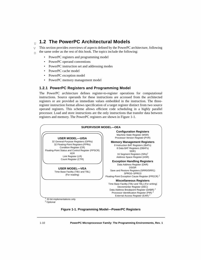
1-10 PowerPC Microprocessor Family: The Programming Environments, Rev. 1
1.2 The PowerPC Architectural ModelsThis section provides overviews of aspects defined by the PowerPC architecture, followingthe same order as the rest of this book. The topics include the following:
• PowerPC registers and programming model• PowerPC operand conventions• PowerPC instruction set and addressing modes• PowerPC cache model• PowerPC exception model• PowerPC memory management model
1.2.1 PowerPC Registers and Programming ModelThe PowerPC architecture defines register-to-register operations for computationalinstructions. Source operands for these instructions are accessed from the architectedregisters or are provided as immediate values embedded in the instruction. The three-register instruction format allows specification of a target register distinct from two sourceoperand registers. This scheme allows efficient code scheduling in a highly parallelprocessor. Load and store instructions are the only instructions that transfer data betweenregisters and memory. The PowerPC registers are shown in Figure 1-1.
Figure 1-1. Programming Model—PowerPC Registers
U
V
O
USER MODEL—UISA32 General-Purpose Registers (GPRs)
32 Floating-Point Registers (FPRs)Condition Register (CR)
Floating-Point Status and Control Register (FPSCR)XER
Link Register (LR)Count Register (CTR)
SUPERVISOR MODEL—OEA
Configuration RegistersMachine State Register (MSR)
Processor Version Register (PVR)
Memory Management Registers8 Instruction BAT Registers (IBATs)
8 Data BAT Registers (DBATs)SDR1
16 Segment Registers (SRs)1
Address Space Register (ASR)
Exception Handling RegistersData Address Register (DAR)
DSISRSave and Restore Registers (SRR0/SRR1)
SPRG0–SPRG3Floating-Point Exception Cause Register (FPECR) 2
Miscellaneous RegistersTime Base Facility (TBU and TBL) (For writing)
Decrementer Register (DEC)Data Address Breakpoint Register (DABR) 2
Processor Identification Register (PIR) 2
External Access Register (EAR) 2
USER MODEL—VEATime Base Facility (TBU and TBL)
(For reading)
1 32-bit implementations only2 Optional
Chapter 1. Overview 1-11
The programming model incorporates 32 GPRs, 32 FPRs, special-purpose registers(SPRs), and several miscellaneous registers. Each implementation may have its own uniqueset of hardware implementation (HID) registers that are not defined by the architecture.
PowerPC processors have two levels of privilege:
• Supervisor mode—used exclusively by the operating system. Resources defined by the OEA can be accessed only supervisor-level software.
• User mode—used by the application software and operating system software (Only resources defined by the UISA and VEA can be accessed by user-level software)
These two levels govern the access to registers, as shown in Figure 1-1. The division ofprivilege allows the operating system to control the application environment (providingvirtual memory and protecting operating system and critical machine resources).Instructions that control the state of the processor, the address translation mechanism, andsupervisor registers can be executed only when the processor is operating in supervisormode.
• User Instruction Set Architecture Registers—All UISA registers can be accessed by all software with either user or supervisor privileges. These registers include the 32 general-purpose registers (GPRs) and the 32 floating-point registers (FPRs), and other registers used for integer, floating-point, and branch instructions.
• Virtual Environment Architecture Registers—The VEA defines the user-level portion of the time base facility, which consists of the two 32-bit time base registers. These registers can be read by user-level software, but can be written to only by supervisor-level software.
• Operating Environment Architecture Registers—SPRs defined by the OEA are used for system-level operations such as memory management, exception handling, and time-keeping.
The PowerPC architecture also provides room in the SPR space for implementation-specific registers, typically referred to as HID registers. Individual HIDs are not discussedin this manual.
1.2.2 Operand ConventionsOperand conventions are defined in two levels of the PowerPC architecture—userinstruction set architecture (UISA) and virtual environment architecture (VEA). Theseconventions define how data is stored in registers and memory.
1.2.2.1 Byte OrderingThe default mapping for PowerPC processors is big-endian, but the UISA provides theoption of operating in either big- or little-endian mode. Big-endian byte ordering is shownin Figure 1-2.
U
V
O
U
V
U

1-12 PowerPC Microprocessor Family: The Programming Environments, Rev. 1
Figure 1-2. Big-Endian Byte and Bit Ordering
The OEA defines two bits in the MSR for specifying byte ordering—LE (little-endianmode) and ILE (exception little-endian mode). The LE bit specifies whether the processoris configured for big-endian or little-endian mode; the ILE bit specifies the mode when anexception is taken by being copied into the LE bit of the MSR. A value of 0 specifies big-endian mode and a value of 1 specifies little-endian mode.
1.2.2.2 Data Organization in Memory and Data TransfersBytes in memory are numbered consecutively starting with 0. Each number is the addressof the corresponding byte.
Memory operands may be bytes, half words, words, or double words, or, for the load/storestring/multiple instructions, a sequence of bytes or words. The address of a multiple-bytememory operand is the address of its first byte (that is, of its lowest-numbered byte).Operand length is implicit for each instruction.
The operand of a single-register memory access instruction has a natural alignmentboundary equal to the operand length. In other words, the natural address of an operand isan integral multiple of the operand length. A memory operand is said to be aligned if it isaligned at its natural boundary; otherwise it is misaligned.
1.2.2.3 Floating-Point ConventionsThe PowerPC architecture adheres to the IEEE-754 standard for 64- and 32-bit floating-point arithmetic:
• Double-precision arithmetic instructions may have single- or double-precision operands but always produce double-precision results.
• Single-precision arithmetic instructions require all operands to be single-precision values and always produce single-precision results. Single-precision values are stored in double-precision format in the FPRs—these values are rounded such that they can be represented in 32-bit, single-precision format (as they are in memory).
1.2.3 PowerPC Instruction Set and Addressing ModesAll PowerPC instructions are encoded as single-word (32-bit) instructions. Instructionformats are consistent among all instruction types, permitting decoding to occur in parallelwith operand accesses. This fixed instruction length and consistent format greatly simplifiesinstruction pipelining.
Byte 0 Byte 1 Byte N (max)
Big-Endian Byte Ordering
MSB
O
U

Chapter 1. Overview 1-13
1.2.3.1 PowerPC Instruction SetAlthough these categories are not defined by the PowerPC architecture, the PowerPCinstructions can be grouped as follows:
• Integer instructions—These instructions are defined by the UISA. They include computational and logical instructions.
— Integer arithmetic instructions— Integer compare instructions— Logical instructions— Integer rotate and shift instructions
• Floating-point instructions—These instructions, defined by the UISA, include floating-point computational instructions, as well as instructions that manipulate the floating-point status and control register (FPSCR).
— Floating-point arithmetic instructions— Floating-point multiply/add instructions— Floating-point compare instructions— Floating-point status and control instructions— Floating-point move instructions— Optional floating-point instructions
• Load/store instructions—These instructions, defined by the UISA, include integer and floating-point load and store instructions.
— Integer load and store instructions— Integer load and store with byte reverse instructions— Integer load and store multiple instructions— Integer load and store string instructions— Floating-point load and store instructions
• The UISA also provides a set of load/store with reservation instructions (lwarx/ldarx and stwcx./stdcx.) that can be used as primitives for constructing atomic memory operations. These are grouped under synchronization instructions.
• Synchronization instructions—The UISA and VEA define instructions for memory synchronizing, especially useful for multiprocessing:
— Load and store with reservation instructions—These UISA-defined instructions provide primitives for synchronization operations such as test and set, compare and swap, and compare memory.
— The Synchronize instruction (sync)—This UISA-defined instruction is useful for synchronizing load and store operations on a memory bus that is shared by multiple devices.
— Enforce In-Order Execution of I/O (eieio)— The eieio instruction provides an ordering function for the effects of load and store operations executed by a processor.
U
V
1-14 PowerPC Microprocessor Family: The Programming Environments, Rev. 1
• Flow control instructions—These include branching instructions, condition register logical instructions, trap instructions, and other instructions that affect the instruction flow.
— The UISA defines numerous instructions that control the program flow, including branch, trap, and system call instructions as well as instructions that read, write, or manipulate bits in the condition register.
— The OEA defines two flow control instructions that provide system linkage. These instructions are used for entering and returning from supervisor level.
• Processor control instructions—These instructions are used for synchronizing memory accesses and managing caches and translation lookaside buffers (TLBs) (and segment registers in 32-bit implementations). These instructions include move to/from special-purpose register instructions (mtspr and mfspr).
• Memory/cache control instructions—These instructions provide control of caches, TLBs, and segment registers (in 32-bit implementations).
— The VEA defines several cache control instructions.
— The OEA defines one cache control instruction and several memory control instructions.
• External control instructions—The VEA defines two optional instructions for use with special input/output devices.
TEMPORARY 64-BIT BRIDGE
• The 64-bit bridge allows several instructions to be used in 64-bit implementations that are otherwise defined for use in 32-bit implementations only. These include the following:
— Move to Segment Register (mtsr) and Move to Segment Register Indirect (mtsrin)
— Move from Segment Register (mfsr) and Move from Segment Register Indirect (mfsrin)
All four of these instructions are implemented as a group and are never implemented individually. Attempting to execute one of these instructions on a 64-bit implementation on which these instructions are not supported causes program exception.
• The 64-bit bridge also defines two instructions, Move to Segment Register Double Word (mtsrd) and Move to Segment Register Double Word Indexed (mtsrdin) that allow an operating system to write to segment descriptors to support accesses to 64-bit address space.
• Processors that implement the 64-bit bridge can optionally implement the rfi and mtmsr instructions, which otherwise are not supported in the 64-bit architecture.
U
O
V
O
V
O

Chapter 1. Overview 1-15
Note that this grouping of the instructions does not indicate which execution unit executesa particular instruction or group of instructions. This is not defined by the PowerPCarchitecture.
1.2.3.2 Calculating Effective Addresses The effective address (EA), also called the logical address, is the address computed by theprocessor when executing a memory access or branch instruction or when fetching the nextsequential instruction. Unless address translation is disabled, this address is converted bythe MMU to the appropriate physical address. (Note that the architecture specification usesonly the term effective address and not logical address.)
The PowerPC architecture supports the following simple addressing modes for memoryaccess instructions:
• EA = (rA|0) (register indirect)• EA = (rA|0) + offset (including offset = 0) (register indirect with immediate index)• EA = (rA|0) + rB (register indirect with index)
These simple addressing modes allow efficient address generation for memory accesses.
1.2.4 PowerPC Cache ModelThe VEA and OEA portions of the architecture define aspects of cache implementations forPowerPC processors. The PowerPC architecture does not define hardware aspects of cacheimplementations. For example, some PowerPC processors may have separate instructionand data caches (Harvard architecture), while others have a unified cache.
The PowerPC architecture allows implementations to control the following memory accessmodes on a page or block basis:
• Write-back/write-through mode• Caching-inhibited mode• Memory coherency • Guarded/not guarded against speculative accesses
Coherency is maintained on a cache block basis, and cache control instructions performoperations on a cache block basis. The size of the cache block is implementation-dependent. The term cache block should not be confused with the notion of a block inmemory, which is described in Section 1.2.6, “PowerPC Memory Management Model.”
The VEA portion of the PowerPC architecture defines several instructions for cachemanagement. These can be used by user-level software to perform such operations as touchoperations (which cause the cache block to be speculatively loaded), and operations tostore, flush, or clear the contents of a cache block. The OEA portion of the architecturedefines one cache management instruction—the Data Cache Block Invalidate (dcbi)instruction.
U
V
O
O
1-16 PowerPC Microprocessor Family: The Programming Environments, Rev. 1
1.2.5 PowerPC Exception ModelThe PowerPC exception mechanism, defined by the OEA, allows the processor to changeto supervisor state as a result of external signals, errors, or unusual conditions arising in theexecution of instructions. When exceptions occur, information about the state of theprocessor is saved to various registers and the processor begins execution at an address(exception vector) predetermined for each type of exception. Exception handler routinesbegin execution in supervisor mode. The PowerPC exception model is described in detailin Chapter 6, “Exceptions.” Note also that some aspects regarding exception conditions aredefined at other levels of the architecture. For example, floating-point exception conditionsare defined by the UISA, whereas the exception mechanism is defined by the OEA.
PowerPC architecture requires that exceptions be handled in program order (excluding theoptional floating-point imprecise modes and the reset and machine check exception);therefore, although a particular implementation may recognize exception conditions out oforder, they are handled strictly in order. When an instruction-caused exception isrecognized, any unexecuted instructions that appear earlier in the instruction stream,including any that have not yet begun to execute, are required to complete before theexception is taken. Any exceptions caused by those instructions must be handled first.Likewise, exceptions that are asynchronous and precise are recognized when they occur,but are not handled until all instructions currently executing successfully completeprocessing and report their results.
The OEA supports four types of exceptions:
• Synchronous, precise • Synchronous, imprecise• Asynchronous, maskable• Asynchronous, nonmaskable
1.2.6 PowerPC Memory Management ModelThe PowerPC memory management unit (MMU) specifications are provided by thePowerPC OEA. The primary functions of the MMU in a PowerPC processor are to translatelogical (effective) addresses to physical addresses for memory accesses and I/O accesses(most I/O accesses are assumed to be memory-mapped), and to provide access protectionon a block or page basis. Note that many aspects of memory management areimplementation-dependent. The description in Chapter 7, “Memory Management,”describes the conceptual model of a PowerPC MMU; however, PowerPC processors maydiffer in the specific hardware used to implement the MMU model of the OEA.
PowerPC processors require address translation for two types of transactions—instructionaccesses and data accesses to memory (typically generated by load and store instructions).
The memory management specification of the PowerPC OEA includes models for both 64-and 32-bit implementations. The MMU of a 64-bit PowerPC processor provides 264 bytes
O

Chapter 1. Overview 1-17
of logical address space accessible to supervisor and user programs with a 4-Kbyte pagesize and 256-Mbyte segment size.
In 32-bit implementations, the entire 4-Gbyte memory space is defined by sixteen 256-Mbyte segments. Segments are configured through the 16 segment registers. In 64-bitimplementations there are more segments than can be maintained in architecture-definedregisters, so segment descriptors are maintained in segment table entries (STEs) in memoryand are accessed through the use of a hashing algorithm much like that used for accessingpage table entries (PTEs).
PowerPC processors also have a block address translation (BAT) mechanism for mappinglarge blocks of memory. Block sizes range from 128 Kbyte to 256 Mbyte and are software-selectable. In addition, the MMU of 64-bit PowerPC processors uses an interim virtualaddress (80 bits) and hashed page tables in the generation of 64-bit physical addresses.
Two types of accesses generated by PowerPC processors require address translation:instruction accesses, and data accesses to memory generated by load and store instructions.The address translation mechanism is defined in terms of segment tables (or segmentregisters in 32-bit implementations) and page tables used by PowerPC processors to locatethe logical-to-physical address mapping for instruction and data accesses. The segmentinformation translates the logical address to an interim virtual address, and the page tableinformation translates the virtual address to a physical address.
Translation lookaside buffers (TLBs) are commonly implemented in PowerPC processorsto keep recently-used page table entries on-chip. Although their exact characteristics are notspecified by the architecture, the general concepts that are pertinent to the system softwareare described. Similarly, 64-bit implementations may contain segment lookaside buffers(SLBs) on-chip that contain recently-used segment table entries, but for which thePowerPC architecture does not define the exact characteristics.
The block address translation (BAT) mechanism is a software-controlled array that storesthe available block address translations on-chip. BAT array entries are implemented as pairsof BAT registers that are accessible as supervisor special-purpose registers (SPRs); refer toChapter 7, “Memory Management,” for more information.
TEMPORARY 64-BIT BRIDGE
The 64-bit bridge provides resources that may make it easier for a 32-bit operating systemto migrate to a 64-bit processor. The nature of these resources are largely determined bythe fact that in a 32-bit address space, only 16 segment descriptors are required to defineall 4 Gbytes of memory. That is, there are sixteen 256-Mbyte segments, as is the case inthe 32-bit architecture description.

1-18 PowerPC Microprocessor Family: The Programming Environments, Rev. 1
1.3 Changes in This Revision of The Programming Environments Manual
This book reflects changes made to the PowerPC architecture after the publication of Rev. 0of The Programming Environments Manual and before Dec. 13, 1994 (Rev. 0.1). Inaddition, it reflects changes made to the architecture after the publication of Rev. 0.1 of TheProgramming Environments Manual and before Aug. 6, 1996 (Rev. 1). Although there aremany changes in this revision of The Programming Environments Manual, this sectionsummarizes only the most significant changes and clarifications to the architecturespecification. There are three types of substantive changes made from Rev. 0 to Rev. 1.
• The temporary addition of a set of resources for optional implementation in 64-bit processors to simplify the adaptation of 32-bit operating systems. These resources are described briefly in Section 1.3.1, “Changes Related to the Optional 64-Bit Bridge.”
• The phasing out of the direct-store facility. This facility defined segments that were used to generate direct-store interface accesses on the external bus to communicate with specialized I/O devices; it was not optimized for performance in the PowerPC architecture and was present for compatibility with older devices only. As of this revision of the architecture (Rev. 1), direct-store segments are an optional processor feature. However, they are not likely to be supported in future implementations and new software should not use them.
• General additions to and refinements of the architecture specification are summarized in Section 1.3.2, “General Changes to the PowerPC Architecture.”
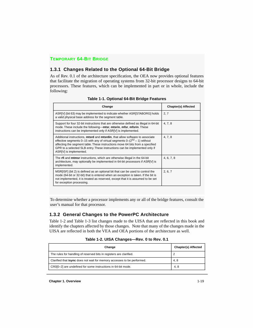
Chapter 1. Overview 1-19
1.3.2 General Changes to the PowerPC ArchitectureTable 1-2 and Table 1-3 list changes made to the UISA that are reflected in this book andidentify the chapters affected by those changes. Note that many of the changes made in theUISA are reflected in both the VEA and OEA portions of the architecture as well.
TEMPORARY 64-BIT BRIDGE
1.3.1 Changes Related to the Optional 64-Bit BridgeAs of Rev. 0.1 of the architecture specification, the OEA now provides optional featuresthat facilitate the migration of operating systems from 32-bit processor designs to 64-bitprocessors. These features, which can be implemented in part or in whole, include thefollowing:
To determine whether a processor implements any or all of the bridge features, consult theuser’s manual for that processor.
Table 1-2. UISA Changes—Rev. 0 to Rev. 0.1
Change Chapter(s) Affected
The rules for handling of reserved bits in registers are clarified. 2
Clarified that isync does not wait for memory accesses to be performed. 4, 8
CR0[0–2] are undefined for some instructions in 64-bit mode. 4, 8
Table 1-1. Optional 64-Bit Bridge Features
Change Chapter(s) Affected
ASR[V] (bit 63) may be implemented to indicate whether ASR[STABORG] holds a valid physical base address for the segment table.
2, 7
Support for four 32-bit instructions that are otherwise defined as illegal in 64-bit mode. These include the following—mtsr, mtsrin, mfsr, mfsrin. These instructions can be implemented only if ASR[V] is implemented.
4, 7, 8
Additional instructions, mtsrd and mtsrdin, that allow software to associate effective segments 0–15 with any of virtual segments 0–(252 – 1) without affecting the segment table. These instructions move 64 bits from a specified GPR to a selected SLB entry. These instructions can be implemented only if ASR[V] is implemented.
4, 7, 8
The rfi and mtmsr instructions, which are otherwise illegal in the 64-bit architecture, may optionally be implemented in 64-bit processors if ASR[V] is implemented.
4, 6, 7, 8
MSR[ISF] (bit 2) is defined as an optional bit that can be used to control the mode (64-bit or 32-bit) that is entered when an exception is taken. If the bit is not implemented, it is treated as reserved, except that it is assumed to be set for exception processing.
2, 6, 7
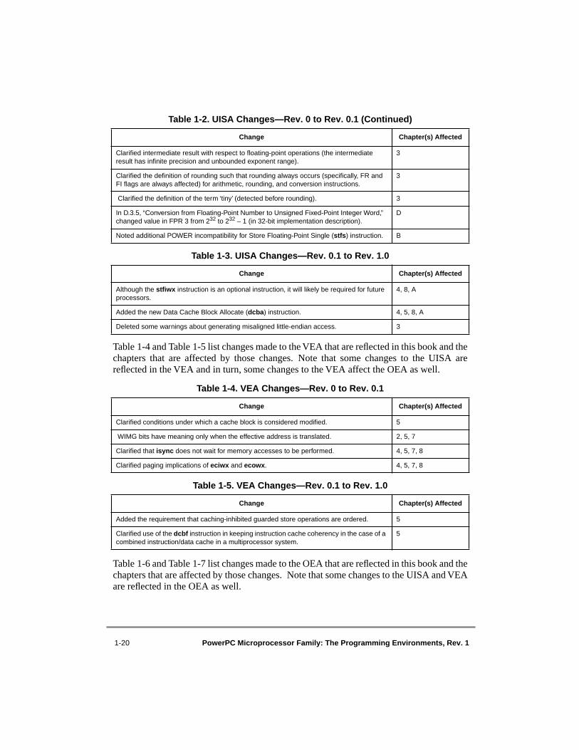
1-20 PowerPC Microprocessor Family: The Programming Environments, Rev. 1
Table 1-4 and Table 1-5 list changes made to the VEA that are reflected in this book and thechapters that are affected by those changes. Note that some changes to the UISA arereflected in the VEA and in turn, some changes to the VEA affect the OEA as well.
Table 1-6 and Table 1-7 list changes made to the OEA that are reflected in this book and thechapters that are affected by those changes. Note that some changes to the UISA and VEAare reflected in the OEA as well.
Clarified intermediate result with respect to floating-point operations (the intermediate result has infinite precision and unbounded exponent range).
3
Clarified the definition of rounding such that rounding always occurs (specifically, FR and FI flags are always affected) for arithmetic, rounding, and conversion instructions.
3
Clarified the definition of the term ‘tiny’ (detected before rounding). 3
In D.3.5, “Conversion from Floating-Point Number to Unsigned Fixed-Point Integer Word,” changed value in FPR 3 from 232 to 232 – 1 (in 32-bit implementation description).
D
Noted additional POWER incompatibility for Store Floating-Point Single (stfs) instruction. B
Table 1-3. UISA Changes—Rev. 0.1 to Rev. 1.0
Change Chapter(s) Affected
Although the stfiwx instruction is an optional instruction, it will likely be required for future processors.
4, 8, A
Added the new Data Cache Block Allocate (dcba) instruction. 4, 5, 8, A
Deleted some warnings about generating misaligned little-endian access. 3
Table 1-4. VEA Changes—Rev. 0 to Rev. 0.1
Change Chapter(s) Affected
Clarified conditions under which a cache block is considered modified. 5
WIMG bits have meaning only when the effective address is translated. 2, 5, 7
Clarified that isync does not wait for memory accesses to be performed. 4, 5, 7, 8
Clarified paging implications of eciwx and ecowx. 4, 5, 7, 8
Table 1-5. VEA Changes—Rev. 0.1 to Rev. 1.0
Change Chapter(s) Affected
Added the requirement that caching-inhibited guarded store operations are ordered. 5
Clarified use of the dcbf instruction in keeping instruction cache coherency in the case of a combined instruction/data cache in a multiprocessor system.
5
Table 1-2. UISA Changes—Rev. 0 to Rev. 0.1 (Continued)
Change Chapter(s) Affected

Chapter 1. Overview 1-21
Table 1-6. OEA Changes—Rev. 0 to Rev. 0.1
Change Chapter(s) Affected
Restricted several aspects of out-of-order operations. 2, 4, 5, 6, 7
Clarified instruction fetching and instruction cache paradoxes. 4, 5
Specified that IBATs contain W and G bits and that software must not write 1s to them. 2, 7
Corrected the description of coherence when the W bit differs among processors. 5
Clarified that referenced and changed bits are set for virtual pages. 7
Revised the description of changed bit setting to avoid depending on the TLB. 7
Tightened the rules for setting the changed bit out of order. 5, 7
Specified which multiple DSISR bits may be set due to simultaneous DSI exceptions. 6
Removed software synchronization requirements for reading the TB and DEC. 2
More flexible DAR setting for a DABR exception. 6
Table 1-7. OEA Changes—Rev. 0.1 to Rev. 1.0
Change Chapter(s) Affected
Changed definition of direct-store segments to an optional processor feature that is not likely to be supported in future implementations and new software should not use it.
2, 6, 7
Changed the ranges of bits saved from MSR to SRR1 (and restored from SRR1 to MSR on rfi[d]) on an exception.
2, 6
Clarified the definition of execution synchronization. Also clarified that the mtmsr and mtmsrd instructions are not execution synchronizing.
2, 4, 8
Clarified the use of memory allocated for predefined uses (including the exception vectors).
6, 7
For 64-bit implementations, changed the definition of the base address for the exception vectors when MSR[IP] = 1 from FFFF_FFFF to 0000–0000.
6
For 64-bit implementations, added the provision for virtual address spaces of 64 bits (as an alternative to the existing 80 bits).
7
Revised the page table update synchronization requirements and recommended code sequences.
7

1-22 PowerPC Microprocessor Family: The Programming Environments, Rev. 1
Chapter 2. PowerPC Register Set 2-1
Chapter 2 PowerPC Register Set2020
This chapter describes the register organization defined by the three levels of the PowerPCarchitecture—user instruction set architecture (UISA), virtual environment architecture(VEA), and operating environment architecture (OEA). The PowerPC architecture definesregister-to-register operations for all computational instructions. Source data for theseinstructions are accessed from the on-chip registers or are provided as immediate valuesembedded in the opcode. The three-register instruction format allows specification of atarget register distinct from the two source registers, thus preserving the original data foruse by other instructions and reducing the number of instructions required for certainoperations. Data is transferred between memory and registers with explicit load and storeinstructions only.
Note that the handling of reserved bits in any register is implementation-dependent.Software is permitted to write any value to a reserved bit in a register. However, asubsequent reading of the reserved bit returns 0 if the value last written to the bit was 0 andreturns an undefined value (may be 0 or 1) otherwise. This means that even if the last valuewritten to a reserved bit was 1, reading that bit may return 0.
2.1 PowerPC UISA Register SetThe PowerPC UISA registers, shown in Figure 2-1, can be accessed by either user- orsupervisor-level instructions (the architecture specification refers to user-level andsupervisor-level as problem state and privileged state respectively). The general-purposeregisters (GPRs) and floating-point registers (FPRs) are accessed as instruction operands.Access to registers can be explicit (that is, through the use of specific instructions for thatpurpose such as Move to Special-Purpose Register (mtspr) and Move from Special-Purpose Register (mfspr) instructions) or implicit as part of the execution of an instruction.Some registers are accessed both explicitly and implicitly.
The number to the right of the register names indicates the number that is used in the syntaxof the instruction operands to access the register (for example, the number used to accessthe XER is SPR 1).
Note that the general-purpose registers (GPRs), link register (LR), and count register (CTR)are 64 bits wide on 64-bit implementations and 32 bits wide on 32-bit implementations.
U
V
O
U
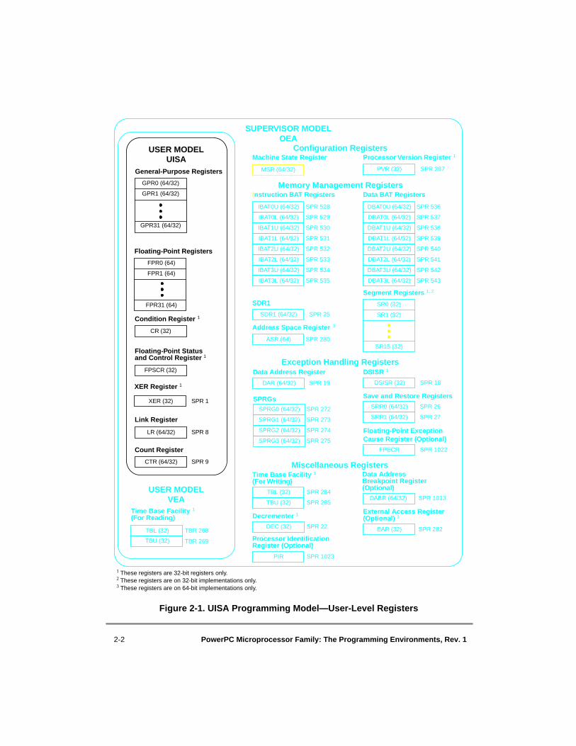
2-2 PowerPC Microprocessor Family: The Programming Environments, Rev. 1
Figure 2-1. UISA Programming Model—User-Level Registers
TBR 268
Time Base Facility 1 (For Reading)
TBL (32)
TBR 269TBU (32)
SUPERVISOR MODELOEA
Machine State Register
MSR (64/32)
Processor Version Register 1
SPR 287PVR (32)
Segment Registers 1, 2
SR0 (32)
SR1 (32)
SR15 (32)
DSISR 1
SPR 18DSISR (32)
Data Address Register
SPR 19DAR (64/32)
Save and Restore Registers
SPR 26SRR0 (64/32)
SPR 27SRR1 (64/32)
SPRGsSPR 272SPRG0 (64/32)
SPR 273SPRG1 (64/32)
SPR 274SPRG2 (64/32)
SPR 275SPRG3 (64/32)
SPR 22
Decrementer 1
DEC (32)
Time Base Facility 1
(For Writing)
SPR 284TBL (32)
SPR 285TBU (32)
SPR 282
External Access Register (Optional) 1
EAR (32)
SDR1
SPR 25SDR1 (64/32)
Address Space Register 3
SPR 280ASR (64)
Instruction BAT Registers
SPR 528IBAT0U (64/32)
SPR 529IBAT0L (64/32)
SPR 530IBAT1U (64/32)
SPR 531IBAT1L (64/32)
SPR 532IBAT2U (64/32)
SPR 533IBAT2L (64/32)
SPR 534IBAT3U (64/32)
SPR 535IBAT3L (64/32)
Data BAT Registers
SPR 536DBAT0U (64/32)
SPR 537DBAT0L (64/32)
SPR 538DBAT1U (64/32)
SPR 539DBAT1L (64/32)
SPR 540DBAT2U (64/32)
SPR 541DBAT2L (64/32)
SPR 542DBAT3U (64/32)
SPR 543DBAT3L (64/32)
Configuration Registers
Memory Management Registers
Exception Handling Registers
Miscellaneous Registers
USER MODELVEA SPR 1013DABR (64/32)
Data Address Breakpoint Register (Optional)
1 These registers are 32-bit registers only.2 These registers are on 32-bit implementations only.3 These registers are on 64-bit implementations only.
SPR 1
USER MODELUISA
Floating-Point Status and Control Register 1
CR (32)
FPSCR (32)
Condition Register 1
GPR0 (64/32)
GPR1 (64/32)
GPR31 (64/32)
FPR0 (64)
FPR1 (64)
FPR31 (64)
General-Purpose Registers
Floating-Point Registers
XER (32)
SPR 8
Link Register
LR (64/32)
SPR 9
Count Register
CTR (64/32)
XER Register 1
Floating-Point Exception Cause Register (Optional)
SPR 1022FPECR
SPR 1023
Processor Identification Register (Optional)
PIR

Chapter 2. PowerPC Register Set 2-3
The user-level registers can be accessed by all software with either user or supervisorprivileges. The user-level register set includes the following:
• General-purpose registers (GPRs). The general-purpose register file consists of 32 GPRs designated as GPR0–GPR31. The GPRs serve as data source or destination registers for all integer instructions and provide data for generating addresses. See Section 2.1.1, “General-Purpose Registers (GPRs),” for more information.
• Floating-point registers (FPRs). The floating-point register file consists of 32 FPRs designated as FPR0–FPR31; these registers serve as the data source or destination for all floating-point instructions. While the floating-point model includes data objects of either single- or double-precision floating-point format, the FPRs only contain data in double-precision format. For more information, see Section 2.1.2, “Floating-Point Registers (FPRs).”
• Condition register (CR). The CR is a 32-bit register, divided into eight 4-bit fields, CR0–CR7, that reflects the results of certain arithmetic operations and provides a mechanism for testing and branching. For more information, see Section 2.1.3, “Condition Register (CR).”
• Floating-point status and control register (FPSCR). The FPSCR contains all floating-point exception signal bits, exception summary bits, exception enable bits, and rounding control bits needed for compliance with the IEEE 754 standard. For more information, see Section 2.1.4, “Floating-Point Status and Control Register (FPSCR).” (Note that the architecture specification refers to exceptions as interrupts.)
• XER register (XER). The XER indicates overflows and carry conditions for integer operations and the number of bytes to be transferred by the load/store string indexed instructions. For more information, see Section 2.1.5, “XER Register (XER).”
• Link register (LR). The LR provides the branch target address for the Branch Conditional to Link Register (bclrx) instructions, and can optionally be used to hold the effective address of the instruction that follows a branch with link update instruction in the instruction stream, typically used for loading the return pointer for a subroutine. For more information, see Section 2.1.6, “Link Register (LR).”
• Count register (CTR). The CTR holds a loop count that can be decremented during execution of appropriately coded branch instructions. The CTR can also provide the branch target address for the Branch Conditional to Count Register (bcctrx) instructions. For more information, see Section 2.1.7, “Count Register (CTR).”
2.1.1 General-Purpose Registers (GPRs)Integer data is manipulated in the processor’s 32 GPRs shown in Figure 2-2. These registersare 64-bit registers in 64-bit implementations and 32-bit registers in 32-bitimplementations. The GPRs are accessed as source and destination registers in theinstruction syntax.

2-4 PowerPC Microprocessor Family: The Programming Environments, Rev. 1
Figure 2-2. General-Purpose Registers (GPRs)
2.1.2 Floating-Point Registers (FPRs)The PowerPC architecture provides thirty-two 64-bit FPRs as shown in Figure 2-3. Theseregisters are accessed as source and destination registers for floating-point instructions.Each FPR supports the double-precision floating-point format. Every instruction thatinterprets the contents of an FPR as a floating-point value uses the double-precisionfloating-point format for this interpretation. Note that FPRs are 64 bits on both 64-bit and32-bit processor implementations.
All floating-point arithmetic instructions operate on data located in FPRs and, with theexception of compare instructions, place the result into an FPR. Information about thestatus of floating-point operations is placed into the FPSCR and in some cases, into the CRafter the completion of instruction execution. For information on how the CR is affected forfloating-point operations, see Section 2.1.3, “Condition Register (CR).”
Load and store double-word instructions transfer 64 bits of data between memory and theFPRs with no conversion. Load single instructions are provided to read a single-precisionfloating-point value from memory, convert it to double-precision floating-point format, andplace it in the target floating-point register. Store single-precision instructions are providedto read a double-precision floating-point value from a floating-point register, convert it tosingle-precision floating-point format, and place it in the target memory location.
Single- and double-precision arithmetic instructions accept values from the FPRs indouble-precision format. For single-precision arithmetic and store instructions, all inputvalues must be representable in single-precision format; otherwise, the result placed intothe target FPR (or the memory location) and the setting of status bits in the FPSCR and inthe condition register (if the instruction’s record bit, Rc, is set) are undefined.
The floating-point arithmetic instructions produce intermediate results that may beregarded as infinitely precise and with unbounded exponent range. This intermediate resultis normalized or denormalized if required, and then rounded to the destination format. Thefinal result is then placed into the target FPR in the double-precision format or in fixed-pointformat, depending on the instruction. Refer to Section 3.3, “Floating-Point ExecutionModels—UISA,” for more information.
GPR0
GPR1
GPR31
0 63
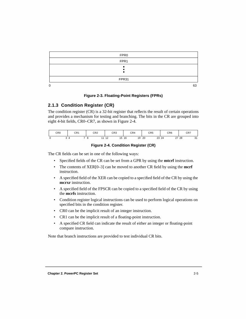
Chapter 2. PowerPC Register Set 2-5
Figure 2-3. Floating-Point Registers (FPRs)
2.1.3 Condition Register (CR)The condition register (CR) is a 32-bit register that reflects the result of certain operationsand provides a mechanism for testing and branching. The bits in the CR are grouped intoeight 4-bit fields, CR0–CR7, as shown in Figure 2-4.
Figure 2-4. Condition Register (CR)
The CR fields can be set in one of the following ways:
• Specified fields of the CR can be set from a GPR by using the mtcrf instruction.
• The contents of XER[0–3] can be moved to another CR field by using the mcrf instruction.
• A specified field of the XER can be copied to a specified field of the CR by using the mcrxr instruction.
• A specified field of the FPSCR can be copied to a specified field of the CR by using the mcrfs instruction.
• Condition register logical instructions can be used to perform logical operations on specified bits in the condition register.
• CR0 can be the implicit result of an integer instruction.
• CR1 can be the implicit result of a floating-point instruction.
• A specified CR field can indicate the result of either an integer or floating-point compare instruction.
Note that branch instructions are provided to test individual CR bits.
FPR0
FPR1
FPR31
0 63
CR0 CR1 CR2 CR3 CR4 CR5 CR6 CR7
0 3 4 7 8 11 12 15 16 19 20 23 24 27 28 31

2-6 PowerPC Microprocessor Family: The Programming Environments, Rev. 1
2.1.3.1 Condition Register CR0 Field DefinitionFor all integer instructions, when the CR is set to reflect the result of the operation (that is,when Rc = 1), and for addic., andi., and andis., the first three bits of CR0 are set by analgebraic comparison of the result to zero; the fourth bit of CR0 is copied from XER[SO].For integer instructions, CR bits 0–3 are set to reflect the result as a signed quantity.
The CR bits are interpreted as shown in Table 2-1. If any portion of the result is undefined,the value placed into the first three bits of CR0 is undefined.
Note that CR0 may not reflect the true (that is, infinitely precise) result if overflow occurs.Also, CR0 bits 0–2 are undefined if Rc = 1 for the mulhw, mulhwu, divw, and divwuinstructions in 64-bit mode.
2.1.3.2 Condition Register CR1 Field DefinitionIn all floating-point instructions when the CR is set to reflect the result of the operation (thatis, when the instruction’s record bit, Rc, is set), CR1 (bits 4–7 of the CR) is copied frombits 0–3 of the FPSCR and indicates the floating-point exception status. For moreinformation about the FPSCR, see Section 2.1.4, “Floating-Point Status and ControlRegister (FPSCR).” The bit settings for the CR1 field are shown in Table 2-2.
Table 2-1. Bit Settings for CR0 Field of CR
CR0 Bit
Description
0 Negative (LT)—This bit is set when the result is negative.
1 Positive (GT)—This bit is set when the result is positive (and not zero).
2 Zero (EQ)—This bit is set when the result is zero.
3 Summary overflow (SO)—This is a copy of the final state of XER[SO] at the completion of the instruction.
Table 2-2. Bit Settings for CR1 Field of CR
CR1 Bit
Description
4 Floating-point exception (FX)—This is a copy of the final state of FPSCR[FX] at the completion of the instruction.
5 Floating-point enabled exception (FEX)—This is a copy of the final state of FPSCR[FEX] at the completion of the instruction.
6 Floating-point invalid exception (VX)—This is a copy of the final state of FPSCR[VX] at the completion of the instruction.
7 Floating-point overflow exception (OX)—This is a copy of the final state of FPSCR[OX] at the completion of the instruction.

Chapter 2. PowerPC Register Set 2-7
2.1.3.3 Condition Register CRn Field—Compare InstructionFor a compare instruction, when a specified CR field is set to reflect the result of thecomparison, the bits of the specified field are interpreted as shown in Table 2-3.
2.1.4 Floating-Point Status and Control Register (FPSCR)The FPSCR, shown in Figure 2-5, contains bits that do the following:
• Record exceptions generated by floating-point operations • Record the type of the result produced by a floating-point operation• Control the rounding mode used by floating-point operations• Enable or disable the reporting of exceptions (invoking the exception handler)
Bits 0–23 are status bits. Bits 24–31 are control bits. Status bits in the FPSCR are updatedat the completion of the instruction execution.
Except for the floating-point enabled exception summary (FEX) and floating-point invalidoperation exception summary (VX), the exception condition bits in the FPSCR (bits 0–12and 21–23) are sticky. Once set, sticky bits remain set until they are cleared by an mcrfs,mtfsfi, mtfsf, or mtfsb0 instruction.
FEX and VX are the logical ORs of other FPSCR bits. Therefore, these two bits are notlisted among the FPSCR bits directly affected by the various instructions.
Table 2-3. CRn Field Bit Settings for Compare Instructions
CRn Bit1
Description2
0 Less than or floating-point less than (LT, FL).For integer compare instructions: rA < SIMM or rB (signed comparison) or
rA < UIMM or rB (unsigned comparison). For floating-point compare instructions: frA < frB.
1 Greater than or floating-point greater than (GT, FG).For integer compare instructions: rA > SIMM or rB (signed comparison) or
rA > UIMM or rB (unsigned comparison). For floating-point compare instructions: frA > frB.
2 Equal or floating-point equal (EQ, FE).For integer compare instructions: rA = SIMM, UIMM, or rB. For floating-point compare instructions: frA = frB.
3 Summary overflow or floating-point unordered (SO, FU).For integer compare instructions: This is a copy of the final state of XER[SO]
at the completion of the instruction. For floating-point compare instructions: One or both of frA and frB is a Not a
Number (NaN).
Notes:1Here, the bit indicates the bit number in any one of the 4-bit subfields, CR0–CR7.2For a complete description of instruction syntax conventions, refer to Table 8-2 on page 8-2.
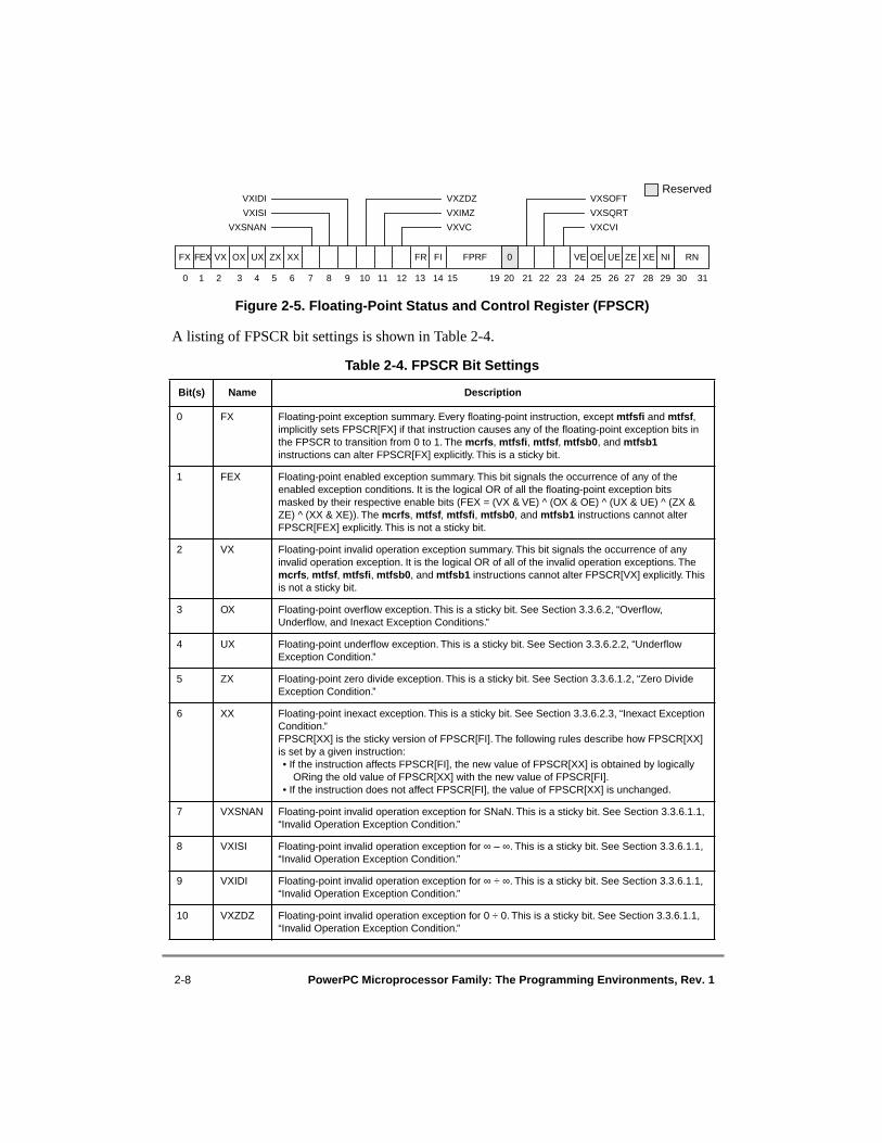
2-8 PowerPC Microprocessor Family: The Programming Environments, Rev. 1
Figure 2-5. Floating-Point Status and Control Register (FPSCR)
A listing of FPSCR bit settings is shown in Table 2-4.
Table 2-4. FPSCR Bit Settings
Bit(s) Name Description
0 FX Floating-point exception summary. Every floating-point instruction, except mtfsfi and mtfsf, implicitly sets FPSCR[FX] if that instruction causes any of the floating-point exception bits in the FPSCR to transition from 0 to 1. The mcrfs, mtfsfi, mtfsf, mtfsb0, and mtfsb1 instructions can alter FPSCR[FX] explicitly. This is a sticky bit.
1 FEX Floating-point enabled exception summary. This bit signals the occurrence of any of the enabled exception conditions. It is the logical OR of all the floating-point exception bits masked by their respective enable bits (FEX = (VX & VE) ^ (OX & OE) ^ (UX & UE) ^ (ZX & ZE) ^ (XX & XE)). The mcrfs, mtfsf, mtfsfi, mtfsb0, and mtfsb1 instructions cannot alter FPSCR[FEX] explicitly. This is not a sticky bit.
2 VX Floating-point invalid operation exception summary. This bit signals the occurrence of any invalid operation exception. It is the logical OR of all of the invalid operation exceptions. The mcrfs, mtfsf, mtfsfi, mtfsb0, and mtfsb1 instructions cannot alter FPSCR[VX] explicitly. This is not a sticky bit.
3 OX Floating-point overflow exception. This is a sticky bit. See Section 3.3.6.2, “Overflow, Underflow, and Inexact Exception Conditions.”
4 UX Floating-point underflow exception. This is a sticky bit. See Section 3.3.6.2.2, “Underflow Exception Condition.”
5 ZX Floating-point zero divide exception. This is a sticky bit. See Section 3.3.6.1.2, “Zero Divide Exception Condition.”
6 XX Floating-point inexact exception. This is a sticky bit. See Section 3.3.6.2.3, “Inexact Exception Condition.” FPSCR[XX] is the sticky version of FPSCR[FI]. The following rules describe how FPSCR[XX] is set by a given instruction:• If the instruction affects FPSCR[FI], the new value of FPSCR[XX] is obtained by logically
ORing the old value of FPSCR[XX] with the new value of FPSCR[FI].• If the instruction does not affect FPSCR[FI], the value of FPSCR[XX] is unchanged.
7 VXSNAN Floating-point invalid operation exception for SNaN. This is a sticky bit. See Section 3.3.6.1.1, “Invalid Operation Exception Condition.”
8 VXISI Floating-point invalid operation exception for ∞ – ∞. This is a sticky bit. See Section 3.3.6.1.1, “Invalid Operation Exception Condition.”
9 VXIDI Floating-point invalid operation exception for ∞ ÷ ∞. This is a sticky bit. See Section 3.3.6.1.1, “Invalid Operation Exception Condition.”
10 VXZDZ Floating-point invalid operation exception for 0 ÷ 0. This is a sticky bit. See Section 3.3.6.1.1, “Invalid Operation Exception Condition.”
0 1 2 3 4 5 6 7 8 9 10 11 12 13 14 15 19 20 21 22 23 24 25 26 27 28 29 30 31
VXIDI
VXISI
VXSNAN
VXZDZ
VXIMZ
VXVC
VXSOFT
VXSQRT
VXCVI
Reserved
FX FEX VX OX UX ZX XX FR FI FPRF 0 VE OE UE ZE XE NI RN

Chapter 2. PowerPC Register Set 2-9
11 VXIMZ Floating-point invalid operation exception for ∞ * 0. This is a sticky bit. See Section 3.3.6.1.1, “Invalid Operation Exception Condition.”
12 VXVC Floating-point invalid operation exception for invalid compare. This is a sticky bit. See Section 3.3.6.1.1, “Invalid Operation Exception Condition.”
13 FR Floating-point fraction rounded. The last arithmetic or rounding and conversion instruction that rounded the intermediate result incremented the fraction. See Section 3.3.5, “Rounding.” This bit is not sticky.
14 FI Floating-point fraction inexact. The last arithmetic or rounding and conversion instruction either rounded the intermediate result (producing an inexact fraction) or caused a disabled overflow exception. See Section 3.3.5, “Rounding.” This is not a sticky bit. For more information regarding the relationship between FPSCR[FI] and FPSCR[XX], see the description of the FPSCR[XX] bit.
15–19 FPRF Floating-point result flags. For arithmetic, rounding, and conversion instructions, the field is based on the result placed into the target register, except that if any portion of the result is undefined, the value placed here is undefined. 15 Floating-point result class descriptor (C). Arithmetic, rounding, and conversion
instructions may set this bit with the FPCC bits to indicate the class of the result as shown in Table 2-5.
16–19 Floating-point condition code (FPCC). Floating-point compare instructions always set one of the FPCC bits to one and the other three FPCC bits to zero. Arithmetic, rounding, and conversion instructions may set the FPCC bits with the C bit to indicate the class of the result. Note that in this case the high-order three bits of the FPCC retain their relational significance indicating that the value is less than, greater than, or equal to zero.16 Floating-point less than or negative (FL or <)17 Floating-point greater than or positive (FG or >)18 Floating-point equal or zero (FE or =)19 Floating-point unordered or NaN (FU or ?)
Note that these are not sticky bits.
20 — Reserved
21 VXSOFT Floating-point invalid operation exception for software request. This is a sticky bit. This bit can be altered only by the mcrfs, mtfsfi, mtfsf, mtfsb0, or mtfsb1 instructions. For more detailed information, refer to Section 3.3.6.1.1, “Invalid Operation Exception Condition.”
22 VXSQRT Floating-point invalid operation exception for invalid square root. This is a sticky bit. For more detailed information, refer to Section 3.3.6.1.1, “Invalid Operation Exception Condition.”
23 VXCVI Floating-point invalid operation exception for invalid integer convert. This is a sticky bit. See Section 3.3.6.1.1, “Invalid Operation Exception Condition.”
24 VE Floating-point invalid operation exception enable. See Section 3.3.6.1.1, “Invalid Operation Exception Condition.”
25 OE IEEE floating-point overflow exception enable. See Section 3.3.6.2, “Overflow, Underflow, and Inexact Exception Conditions.”
26 UE IEEE floating-point underflow exception enable. See Section 3.3.6.2.2, “Underflow Exception Condition.”
27 ZE IEEE floating-point zero divide exception enable. See Section 3.3.6.1.2, “Zero Divide Exception Condition.”
28 XE Floating-point inexact exception enable. See Section 3.3.6.2.3, “Inexact Exception Condition.”
Table 2-4. FPSCR Bit Settings (Continued)
Bit(s) Name Description

2-10 PowerPC Microprocessor Family: The Programming Environments, Rev. 1
Table 2-5 illustrates the floating-point result flags used by PowerPC processors. The resultflags correspond to FPSCR bits 15–19.
29 NI Floating-point non-IEEE mode. If this bit is set, results need not conform with IEEE standards and the other FPSCR bits may have meanings other than those described here. If the bit is set and if all implementation-specific requirements are met and if an IEEE-conforming result of a floating-point operation would be a denormalized number, the result produced is zero (retaining the sign of the denormalized number). Any other effects associated with setting this bit are described in the user’s manual for the implementation (the effects are implementation-dependent).
30–31 RN Floating-point rounding control. See Section 3.3.5, “Rounding.”00 Round to nearest 01 Round toward zero 10 Round toward +infinity11 Round toward –infinity
Table 2-5. Floating-Point Result Flags in FPSCR
Result Flags (Bits 15–19)Result Value Class
C < > = ?
1 0 0 0 1 Quiet NaN
0 1 0 0 1 –Infinity
0 1 0 0 0 –Normalized number
1 1 0 0 0 –Denormalized number
1 0 0 1 0 –Zero
0 0 0 1 0 +Zero
1 0 1 0 0 +Denormalized number
0 0 1 0 0 +Normalized number
0 0 1 0 1 +Infinity
Table 2-4. FPSCR Bit Settings (Continued)
Bit(s) Name Description

Chapter 2. PowerPC Register Set 2-11
2.1.5 XER Register (XER)The XER register (XER) is a 32-bit, user-level register shown in Figure 2-6.
.
Figure 2-6. XER Register
The bit definitions for XER, shown in Table 2-6, are based on the operation of aninstruction considered as a whole, not on intermediate results. For example, the result of theSubtract from Carrying (subfcx) instruction is specified as the sum of three values. Thisinstruction sets bits in the XER based on the entire operation, not on an intermediate sum.
2.1.6 Link Register (LR)The link register (LR) is a 64-bit register in 64-bit implementations and a 32-bit register in32-bit implementations. The LR supplies the branch target address for the BranchConditional to Link Register (bclrx) instructions, and in the case of a branch with linkupdate instruction, can be used to hold the logical address of the instruction that follows the
Table 2-6. XER Bit Definitions
Bit(s) Name Description
0 SO Summary overflow. The summary overflow bit (SO) is set whenever an instruction (except mtspr) sets the overflow bit (OV). Once set, the SO bit remains set until it is cleared by an mtspr instruction (specifying the XER) or an mcrxr instruction. It is not altered by compare instructions, nor by other instructions (except mtspr to the XER, and mcrxr) that cannot overflow. Executing an mtspr instruction to the XER, supplying the values zero for SO and one for OV, causes SO to be cleared and OV to be set.
1 OV Overflow. The overflow bit (OV) is set to indicate that an overflow has occurred during execution of an instruction. Add, subtract from, and negate instructions having OE = 1 set the OV bit if the carry out of the msb is not equal to the carry out of the msb + 1, and clear it otherwise. Multiply low and divide instructions having OE = 1 set the OV bit if the result cannot be represented in 64 bits (mulld, divd, divdu) or in 32 bits (mullw, divw, divwu), and clear it otherwise. The OV bit is not altered by compare instructions that cannot overflow (except mtspr to the XER, and mcrxr).
2 CA Carry. The carry bit (CA) is set during execution of the following instructions: • Add carrying, subtract from carrying, add extended, and subtract from extended instructions
set CA if there is a carry out of the msb, and clear it otherwise. • Shift right algebraic instructions set CA if any 1 bits have been shifted out of a negative
operand, and clear it otherwise. The CA bit is not altered by compare instructions, nor by other instructions that cannot carry (except shift right algebraic, mtspr to the XER, and mcrxr).
3–24 — Reserved
25–31 This field specifies the number of bytes to be transferred by a Load String Word Indexed (lswx) or Store String Word Indexed (stswx) instruction.
Reserved
SO OV CA 0 0000 0000 0000 0000 0000 0 Byte count
0 1 2 3 24 25 31
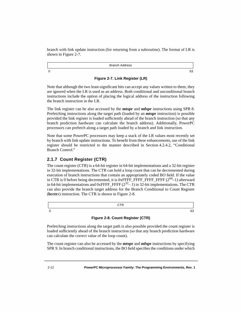
2-12 PowerPC Microprocessor Family: The Programming Environments, Rev. 1
branch with link update instruction (for returning from a subroutine). The format of LR isshown in Figure 2-7.
Figure 2-7. Link Register (LR)
Note that although the two least-significant bits can accept any values written to them, theyare ignored when the LR is used as an address. Both conditional and unconditional branchinstructions include the option of placing the logical address of the instruction followingthe branch instruction in the LR.
The link register can be also accessed by the mtspr and mfspr instructions using SPR 8.Prefetching instructions along the target path (loaded by an mtspr instruction) is possibleprovided the link register is loaded sufficiently ahead of the branch instruction (so that anybranch prediction hardware can calculate the branch address). Additionally, PowerPCprocessors can prefetch along a target path loaded by a branch and link instruction.
Note that some PowerPC processors may keep a stack of the LR values most recently setby branch with link update instructions. To benefit from these enhancements, use of the linkregister should be restricted to the manner described in Section 4.2.4.2, “ConditionalBranch Control.”
2.1.7 Count Register (CTR)The count register (CTR) is a 64-bit register in 64-bit implementations and a 32-bit registerin 32-bit implementations. The CTR can hold a loop count that can be decremented duringexecution of branch instructions that contain an appropriately coded BO field. If the valuein CTR is 0 before being decremented, it is 0xFFFF_FFFF_FFFF_FFFF (264–1) afterwardin 64-bit implementations and 0xFFFF_FFFF (232– 1) in 32-bit implementations. The CTRcan also provide the branch target address for the Branch Conditional to Count Register(bcctrx) instruction. The CTR is shown in Figure 2-8.
Figure 2-8. Count Register (CTR)
Prefetching instructions along the target path is also possible provided the count register isloaded sufficiently ahead of the branch instruction (so that any branch prediction hardwarecan calculate the correct value of the loop count).
The count register can also be accessed by the mtspr and mfspr instructions by specifyingSPR 9. In branch conditional instructions, the BO field specifies the conditions under which
Branch Address
0 63
CTR
0 63

Chapter 2. PowerPC Register Set 2-13
the branch is taken. The first four bits of the BO field specify how the branch is affected byor affects the CR and the CTR. The encoding for the BO field is shown in Table 2-7.
2.2 PowerPC VEA Register Set—Time BaseThe PowerPC virtual environment architecture (VEA) defines registers in addition to thosedefined by the UISA. The PowerPC VEA register set can be accessed by all software witheither user- or supervisor-level privileges. Figure 2-9 provides a graphic illustration of thePowerPC VEA register set. Note that the following programming model is similar to thatfound in Figure 2-1, however, the PowerPC VEA registers are now included.
The PowerPC VEA introduces the time base facility (TB), a 64-bit structure that consistsof two 32-bit registers—time base upper (TBU) and time base lower (TBL). Note that thetime base registers can be accessed by both user- and supervisor-level instructions. In thecontext of the VEA, user-level applications are permitted read-only access to the TB. TheOEA defines supervisor-level access to the TB for writing values to the TB. SeeSection 2.3.13, “Time Base Facility (TB)—OEA,” for more information.
In Figure 2-9, the numbers to the right of the register name indicates the number that is usedin the syntax of the instruction operands to access the register (for example, the numberused to access the XER is SPR 1).
Note that the general-purpose registers (GPRs), link register (LR), and count register (CTR)are 64 bits on 64-bit implementations and 32 bits on 32-bit implementations. Theseregisters are described fully in Section 2.1, “PowerPC UISA Register Set.”
Table 2-7. BO Operand Encodings
BO Description
0000y Decrement the CTR, then branch if the decremented CTR ≠ 0 and the condition is FALSE.
0001y Decrement the CTR, then branch if the decremented CTR = 0 and the condition is FALSE.
001zy Branch if the condition is FALSE.
0100y Decrement the CTR, then branch if the decremented CTR ≠ 0 and the condition is TRUE.
0101y Decrement the CTR, then branch if the decremented CTR = 0 and the condition is TRUE.
011zy Branch if the condition is TRUE.
1z00y Decrement the CTR, then branch if the decremented CTR ≠ 0.
1z01y Decrement the CTR, then branch if the decremented CTR = 0.
1z1zz Branch always.
Notes: The y bit provides a hint about whether a conditional branch is likely to be taken and is used by some PowerPC implementations to improve performance. Other implementations may ignore the y bit.
The z indicates a bit that is ignored. The z bits should be cleared (zero), as they may be assigned a meaning in a future version of the PowerPC UISA.
V

2-14 PowerPC Microprocessor Family: The Programming Environments, Rev. 1
Figure 2-9. VEA Programming Model—User-Level Registers Plus Time Base
TBR 2684
Time Base Facility 1 (For Reading)
TBL (32)
TBR 269TBU (32)
USER MODELVEA
1 These registers are 32-bit registers only.2 These registers are on 32-bit implementations only.3 These registers are on 64-bit implementations only.4 In 64-bit implementations, TBR268 is read as a 64-bit value.
SPR 1
USER MODELUISA
Floating-Point Status and Control Register 1
CR (32)
FPSCR (32)
Condition Register 1
GPR0 (64/32)
GPR1 (64/32)
GPR31 (64/32)
FPR0 (64)
FPR1 (64)
FPR31 (64)
General-Purpose Registers
Floating-Point Registers
XER (32)
SPR 8
Link Register
LR (64/32)
SPR 9
Count Register
CTR (64/32)
XER Register 1
SUPERVISOR MODELOEA
Machine State Register
MSR (64/32)
Processor Version Register 1
SPR 287PVR (32)
Segment Registers 1, 2
SR0 (32)
SR1 (32)
SR15 (32)
DSISR 1
SPR 18DSISR (32)
Data Address Register
SPR 19DAR (64/32)
Save and Restore Registers
SPR 26SRR0 (64/32)
SPR 27SRR1 (64/32)
SPRGsSPR 272SPRG0 (64/32)
SPR 273SPRG1 (64/32)
SPR 274SPRG2 (64/32)
SPR 275SPRG3 (64/32)
SPR 22
Decrementer 1
DEC (32)
Time Base Facility 1
(For Writing)
SPR 284TBL (32)
SPR 285TBU (32)
SPR 282
External Access Register (Optional) 1
EAR (32)
SDR1
SPR 25SDR1 (64/32)
Address Space Register 3
SPR 280ASR (64)
Instruction BAT Registers
SPR 528IBAT0U (64/32)
SPR 529IBAT0L (64/32)
SPR 530IBAT1U (64/32)
SPR 531IBAT1L (64/32)
SPR 532IBAT2U (64/32)
SPR 533IBAT2L (64/32)
SPR 534IBAT3U (64/32)
SPR 535IBAT3L (64/32)
Data BAT Registers
SPR 536DBAT0U (64/32)
SPR 537DBAT0L (64/32)
SPR 538DBAT1U (64/32)
SPR 539DBAT1L (64/32)
SPR 540DBAT2U (64/32)
SPR 541DBAT2L (64/32)
SPR 542DBAT3U (64/32)
SPR 543DBAT3L (64/32)
Configuration Registers
Memory Management Registers
Exception Handling Registers
Miscellaneous Registers
SPR 1013DABR (64/32)
Data Address Breakpoint Register (Optional)
Floating-Point Exception Cause Register (Optional)
SPR 1022FPECR
SPR 1023
Processor Identification Register (Optional)
PIR

Chapter 2. PowerPC Register Set 2-15
The time base (TB), shown in Figure 2-10, is a 64-bit structure that contains a 64-bitunsigned integer that is incremented periodically. Each increment adds 1 to the low-orderbit (bit 31 of TBL). The frequency at which the counter is incremented is implementation-dependent.
Figure 2-10. Time Base (TB)
The TB increments until its value becomes 0xFFFF_FFFF_FFFF_FFFF (264 – 1). At thenext increment its value becomes 0x0000_0000_0000_0000. Note that there is no explicitindication that this has occurred (that is, no exception is generated).
The period of the time base depends on the driving frequency. The TB is implemented suchthat the following requirements are satisfied:
1. Loading a GPR from the time base has no effect on the accuracy of the time base.
2. Storing a GPR to the time base replaces the value in the time base with the value in the GPR.
The PowerPC VEA does not specify a relationship between the frequency at which the timebase is updated and other frequencies, such as the processor clock. The TB updatefrequency is not required to be constant; however, for the system software to maintain timeof day and operate interval timers, one of two things is required:
• The system provides an implementation-dependent exception to software whenever the update frequency of the time base changes and a means to determine the current update frequency; or
• The system software controls the update frequency of the time base.
Note that if the operating system initializes the TB to some reasonable value and the updatefrequency of the TB is constant, the TB can be used as a source of values that increase at aconstant rate, such as for time stamps in trace entries.
Even if the update frequency is not constant, values read from the TB are monotonicallyincreasing (except when the TB wraps from 264 – 1 to 0). If a trace entry is recorded eachtime the update frequency changes, the sequence of TB values can be postprocessed tobecome actual time values.
However, successive readings of the time base may return identical values due toimplementation-dependent factors such as a low update frequency or initialization.
0 31 0 31
TBU—Upper 32 bits of time base TBL—Lower 32 bits of time base
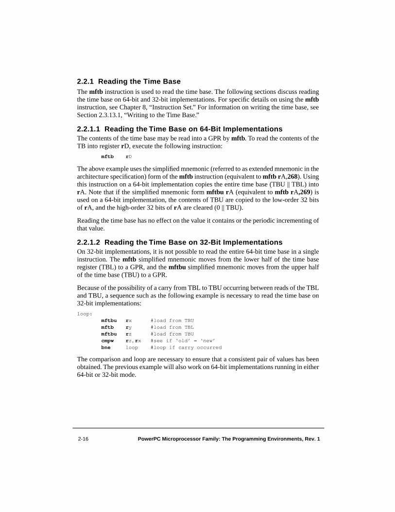
2-16 PowerPC Microprocessor Family: The Programming Environments, Rev. 1
2.2.1 Reading the Time BaseThe mftb instruction is used to read the time base. The following sections discuss readingthe time base on 64-bit and 32-bit implementations. For specific details on using the mftbinstruction, see Chapter 8, “Instruction Set.” For information on writing the time base, seeSection 2.3.13.1, “Writing to the Time Base.”
2.2.1.1 Reading the Time Base on 64-Bit ImplementationsThe contents of the time base may be read into a GPR by mftb. To read the contents of theTB into register rD, execute the following instruction:
mftb rD
The above example uses the simplified mnemonic (referred to as extended mnemonic in thearchitecture specification) form of the mftb instruction (equivalent to mftb rA,268). Usingthis instruction on a 64-bit implementation copies the entire time base (TBU || TBL) intorA. Note that if the simplified mnemonic form mftbu rA (equivalent to mftb rA,269) isused on a 64-bit implementation, the contents of TBU are copied to the low-order 32 bitsof rA, and the high-order 32 bits of rA are cleared (0 || TBU).
Reading the time base has no effect on the value it contains or the periodic incrementing ofthat value.
2.2.1.2 Reading the Time Base on 32-Bit ImplementationsOn 32-bit implementations, it is not possible to read the entire 64-bit time base in a singleinstruction. The mftb simplified mnemonic moves from the lower half of the time baseregister (TBL) to a GPR, and the mftbu simplified mnemonic moves from the upper halfof the time base (TBU) to a GPR.
Because of the possibility of a carry from TBL to TBU occurring between reads of the TBLand TBU, a sequence such as the following example is necessary to read the time base on32-bit implementations:
loop:mftbu rx #load from TBUmftb ry #load from TBLmftbu rz #load from TBUcmpw rz,rx #see if ‘old’ = ‘new’bne loop #loop if carry occurred
The comparison and loop are necessary to ensure that a consistent pair of values has beenobtained. The previous example will also work on 64-bit implementations running in either64-bit or 32-bit mode.
Chapter 2. PowerPC Register Set 2-17
2.2.2 Computing Time of Day from the Time BaseSince the update frequency of the time base is system-dependent, the algorithm forconverting the current value in the time base to time of day is also system-dependent.
In a system in which the update frequency of the time base may change over time, it is notpossible to convert an isolated time base value into time of day. Instead, a time base valuehas meaning only with respect to the current update frequency and the time of day that theupdate frequency was last changed. Each time the update frequency changes, either thesystem software is notified of the change via an exception, or else the change was instigatedby the system software itself. At each such change, the system software must compute thecurrent time of day using the old update frequency, compute a new value of ticks-per-second for the new frequency, and save the time of day, time base value, and tick rate.Subsequent calls to compute time of day use the current time base value and the saved data.
A generalized service to compute time of day could take the following as input:
• Time of day at beginning of current epoch• Time base value at beginning of current epoch• Time base update frequency• Time base value for which time of day is desired
For a PowerPC system in which the time base update frequency does not vary, the first threeinputs would be constant.
2.3 PowerPC OEA Register SetThe PowerPC operating environment architecture (OEA) completes the discussion ofPowerPC registers. Figure 2-11 shows a graphic representation of the entire PowerPCregister set—UISA, VEA, and OEA. In Figure 2-11 the numbers to the right of the registername indicates the number that is used in the syntax of the instruction operands to accessthe register (for example, the number used to access the XER is SPR 1).
All of the SPRs in the OEA can be accessed only by supervisor-level instructions; anyattempt to access these SPRs with user-level instructions results in a supervisor-levelexception. Some SPRs are implementation-specific. In some cases, not all of a register’sbits are implemented in hardware.
If a PowerPC processor executes an mtspr/mfspr instruction with an undefined SPRencoding, it takes (depending on the implementation) an illegal instruction programexception, a privileged instruction program exception, or the results are boundedlyundefined. See Section 6.4.7, “Program Exception (0x00700),” for more information.
Note that the GPRs, LR, CTR, TBL, MSR, DAR, SDR1, SRR0, SRR1, andSPRG0–SPRG3 are 64 bits wide on 64-bit implementations and 32 bits wide on 32-bitimplementations.
O
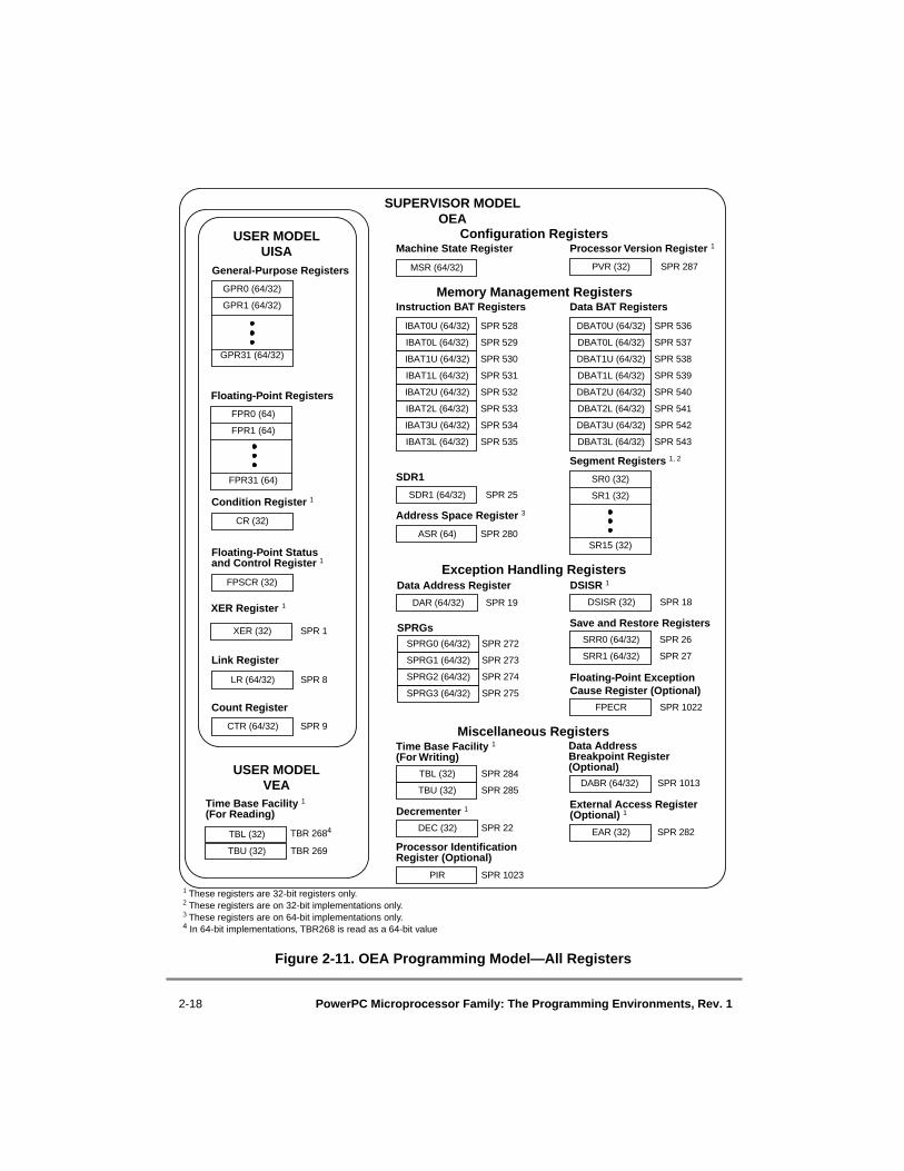
2-18 PowerPC Microprocessor Family: The Programming Environments, Rev. 1
Figure 2-11. OEA Programming Model—All Registers
TBR 2684
Time Base Facility 1 (For Reading)
TBL (32)
TBR 269TBU (32)
SUPERVISOR MODELOEA
Machine State Register
MSR (64/32)
Processor Version Register 1
SPR 287PVR (32)
Segment Registers 1, 2
SR0 (32)
SR1 (32)
SR15 (32)
DSISR 1
SPR 18DSISR (32)
Data Address Register
SPR 19DAR (64/32)
Save and Restore Registers
SPR 26SRR0 (64/32)
SPR 27SRR1 (64/32)
SPRGsSPR 272SPRG0 (64/32)
SPR 273SPRG1 (64/32)
SPR 274SPRG2 (64/32)
SPR 275SPRG3 (64/32)
SPR 22
Decrementer 1
DEC (32)
Time Base Facility 1(For Writing)
SPR 284TBL (32)
SPR 285TBU (32)
SPR 282
External Access Register (Optional) 1
EAR (32)
SDR1
SPR 25SDR1 (64/32)
Address Space Register 3
SPR 280ASR (64)
Instruction BAT Registers
SPR 528IBAT0U (64/32)
SPR 529IBAT0L (64/32)
SPR 530IBAT1U (64/32)
SPR 531IBAT1L (64/32)
SPR 532IBAT2U (64/32)
SPR 533IBAT2L (64/32)
SPR 534IBAT3U (64/32)
SPR 535IBAT3L (64/32)
Data BAT Registers
SPR 536DBAT0U (64/32)
SPR 537DBAT0L (64/32)
SPR 538DBAT1U (64/32)
SPR 539DBAT1L (64/32)
SPR 540DBAT2U (64/32)
SPR 541DBAT2L (64/32)
SPR 542DBAT3U (64/32)
SPR 543DBAT3L (64/32)
Configuration Registers
Memory Management Registers
Exception Handling Registers
Miscellaneous Registers
USER MODELVEA SPR 1013DABR (64/32)
Data Address Breakpoint Register (Optional)
1 These registers are 32-bit registers only.2 These registers are on 32-bit implementations only.3 These registers are on 64-bit implementations only.4 In 64-bit implementations, TBR268 is read as a 64-bit value
SPR 1
USER MODELUISA
Floating-Point Status and Control Register 1
CR (32)
FPSCR (32)
Condition Register 1
GPR0 (64/32)
GPR1 (64/32)
GPR31 (64/32)
FPR0 (64)
FPR1 (64)
FPR31 (64)
General-Purpose Registers
Floating-Point Registers
XER (32)
SPR 8
Link Register
LR (64/32)
SPR 9
Count Register
CTR (64/32)
XER Register 1
Floating-Point Exception Cause Register (Optional)
SPR 1022FPECR
SPR 1023
Processor Identification Register (Optional)
PIR

Chapter 2. PowerPC Register Set 2-19
A description of the PowerPC OEA supervisor-level registers follows:
• Configuration registers
— Machine state register (MSR). The MSR defines the state of the processor. The MSR can be modified by the Move to Machine State Register (mtmsrd [or mtmsr]), System Call (sc), and Return from Interrupt (rfid [or rfi]) instructions. It can be read by the Move from Machine State Register (mfmsr) instruction. For more information, see Section 2.3.1, “Machine State Register (MSR).”
— Processor version register (PVR). This register is a read-only register that identifies the version (model) and revision level of the PowerPC processor. For more information, see Section 2.3.2, “Processor Version Register (PVR).”
• Memory management registers
— Block-address translation (BAT) registers. The PowerPC OEA includes eight block-address translation registers (BATs), consisting of four pairs of instruction BATs (IBAT0U–IBAT3U and IBAT0L–IBAT3L) and four pairs of data BATs (DBAT0U–DBAT3U and DBAT0L–DBAT3L). See Figure 2-11 for a list of the SPR numbers for the BAT registers. Refer to Section 2.3.3, “BAT Registers,” for more information.
— SDR1. The SDR1 register specifies the page table base address used in virtual-to-physical address translation. For more information, see Section 2.3.4, “SDR1.” (Note that physical address is referred to as real address in the architecture specification.)
— Address space register (ASR). The ASR holds the physical address of the segment table. It is found only on 64-bit implementations. For more information, see Section 2.3.5, “Address Space Register (ASR).”
— Segment registers (SR). The PowerPC OEA defines sixteen 32-bit segment registers (SR0–SR15). Note that the SRs are implemented on 32-bit implementations only. The fields in the segment register are interpreted differently depending on the value of bit 0. For more information, see Section 2.3.6, “Segment Registers.” Note that the 64-bit bridge facility defines a way in which 64-bit implementations can use 16 SLB entries as if they were segment registers. See Chapter 7, “Memory Management,” for more detailed information about the bridge facility.
• Exception handling registers
— Data address register (DAR). After a DSI or an alignment exception, DAR is set to the effective address generated by the faulting instruction. For more information, see Section 2.3.7, “Data Address Register (DAR).”
— SPRG0–SPRG3. The SPRG0–SPRG3 registers are provided for operating system use. For more information, see Section 2.3.8, “SPRG0–SPRG3.”
— DSISR. The DSISR defines the cause of DSI and alignment exceptions. For more information, refer to Section 2.3.9, “DSISR.”
2-20 PowerPC Microprocessor Family: The Programming Environments, Rev. 1
— Machine status save/restore register 0 (SRR0). The SRR0 register is used to save machine status on exceptions and to restore machine status when an rfid (or rfi) instruction is executed. For more information, see Section 2.3.10, “Machine Status Save/Restore Register 0 (SRR0).”
— Machine status save/restore register 1 (SRR1). The SRR1 register is used to save machine status on exceptions and to restore machine status when an rfid (or rfi) instruction is executed. For more information, see Section 2.3.11, “Machine Status Save/Restore Register 1 (SRR1).”
— Floating-point exception cause register (FPECR). This optional register is used to identify the cause of a floating-point exception.
• Miscellaneous registers
— Time base (TB). The TB is a 64-bit structure that maintains the time of day and operates interval timers. The TB consists of two 32-bit registers—time base upper (TBU) and time base lower (TBL). Note that the time base registers can be accessed by both user- and supervisor-level instructions. For more information, see Section 2.3.13, “Time Base Facility (TB)—OEA” and Section 2.2, “PowerPC VEA Register Set—Time Base.”
— Decrementer register (DEC). This register is a 32-bit decrementing counter that provides a mechanism for causing a decrementer exception after a programmable delay; the frequency is a subdivision of the processor clock. For more information, see Section 2.3.14, “Decrementer Register (DEC).”
— External access register (EAR). This optional register is used in conjunction with the eciwx and ecowx instructions. Note that the EAR register and the eciwx and ecowx instructions are optional in the PowerPC architecture and may not be supported in all PowerPC processors that implement the OEA. For more information about the external control facility, see Section 4.3.4, “External Control Instructions.”
— Data address breakpoint register (DABR). This optional register is used to control the data address breakpoint facility. Note that the DABR is optional in the PowerPC architecture and may not be supported in all PowerPC processors that implement the OEA. For more information about the data address breakpoint facility, see Section 6.4.3, “DSI Exception (0x00300).”
— Processor identification register (PIR). This optional register is used to hold a value that distinguishes an individual processor in a multiprocessor environment.
2.3.1 Machine State Register (MSR)The machine state register (MSR) is a 64-bit register on 64-bit implementations (seeFigure 2-12) and a 32-bit register in 32-bit implementations (see Figure 2-13). The MSRdefines the state of the processor. When an exception occurs, MSR bits, as described inTable 2-8, are altered as determined by the exception. The MSR can also be modified bythe mtmsrd (or mtmsr), sc, and rfid (or rfi) instructions. It can be read by the mfmsrinstruction.

Chapter 2. PowerPC Register Set 2-21
Figure 2-12. Machine State Register (MSR)—64-Bit Implementations
Figure 2-13. Machine State Register (MSR)—32-Bit Implementations
Table 2-8 shows the bit definitions for the MSR.
Table 2-8. MSR Bit Settings
Bit(s)Name Description
64 Bit 32 Bit
0 — SF Sixty-four bit mode0 The 64-bit processor runs in 32-bit mode.1 The 64-bit processor runs in 64-bit mode. Note that this is the default
setting.
1 — — Reserved
TEMPORARY 64-BIT BRIDGE
2 — ISF Exception 64-bit mode (optional). When an exception occurs, this bit is copied into MSR[SF] to select 64- or 32-bit mode for the context established by the exception.Note: If the bridge function is not implemented, this bit is treated as reserved.
3–44 0–12 — Reserved
45 13 POW Power management enable0 Power management disabled (normal operation mode)1 Power management enabled (reduced power mode)Note: Power management functions are implementation-dependent. If the function is not implemented, this bit is treated as reserved.
46 14 — Reserved
47 15 ILE Exception little-endian mode. When an exception occurs, this bit is copied into MSR[LE] to select the endian mode for the context established by the exception.
48 16 EE External interrupt enable 0 While the bit is cleared, the processor delays recognition of external
interrupts and decrementer exception conditions. 1 The processor is enabled to take an external interrupt or the decrementer
exception.
0 1 2 3 44 45 46 47 48 49 50 51 52 53 54 55 56 57 58 59 60 61 62 63
POW 0 ILE EE PR FP ME FE0 SE BE FE1 0 IP IR DR 00 RI LESF 0 ISF* 0 0000 ... 0000 0
Temporary 64-Bit Bridge* Note that the ISF bit is optional and implemented only as part of the 64-bit bridge. For information see Table 2-8.
0 12 13 14 15 16 17 18 19 20 21 22 23 24 25 26 27 28 29 30 31
Reserved
0000 0000 0000 0 POW 0 ILE EE PR FP ME FE0 SE BE FE1 0 IP IR DR 00 RI LE

2-22 PowerPC Microprocessor Family: The Programming Environments, Rev. 1
49 17 PR Privilege level 0 The processor can execute both user- and supervisor-level instructions.1 The processor can only execute user-level instructions.
50 18 FP Floating-point available 0 The processor prevents dispatch of floating-point instructions, including
floating-point loads, stores, and moves.1 The processor can execute floating-point instructions.
51 19 ME Machine check enable 0 Machine check exceptions are disabled. 1 Machine check exceptions are enabled.
52 20 FE0 Floating-point exception mode 0 (see Table 2-9).
53 21 SE Single-step trace enable (Optional)0 The processor executes instructions normally. 1 The processor generates a single-step trace exception upon the
successful execution of the next instruction.Note: If the function is not implemented, this bit is treated as reserved.
54 22 BE Branch trace enable (Optional)0 The processor executes branch instructions normally. 1 The processor generates a branch trace exception after completing the
execution of a branch instruction, regardless of whether the branch was taken.
Note: If the function is not implemented, this bit is treated as reserved.
55 23 FE1 Floating-point exception mode 1 (See Table 2-9).
56 24 — Reserved
57 25 IP Exception prefix. The setting of this bit specifies whether an exception vector offset is prepended with Fs or 0s. In the following description, nnnnn is the offset of the exception vector. See Table 6-2.0 Exceptions are vectored to the physical address 0x000n_nnnn in 32-bit
implementations and 0x0000_0000_000n_nnnn in 64-bit implementations.
1 Exceptions are vectored to the physical address 0xFFFn_nnnn in 32-bit implementations and 0x0000_0000_FFFn_nnnn in 64-bit implementations.
In most systems, IP is set to 1 during system initialization, and then cleared to 0 when initialization is complete.
58 26 IR Instruction address translation 0 Instruction address translation is disabled. 1 Instruction address translation is enabled.For more information, see Chapter 7, “Memory Management.”
59 27 DR Data address translation 0 Data address translation is disabled. 1 Data address translation is enabled.For more information, see Chapter 7, “Memory Management.”
60–61 28–29 — Reserved
Table 2-8. MSR Bit Settings (Continued)
Bit(s)Name Description
64 Bit 32 Bit

Chapter 2. PowerPC Register Set 2-23
The floating-point exception mode bits (FE0–FE1) are interpreted as shown in Table 2-9.
Table 2-10 indicates the initial state of the MSR at power up.
62 30 RI Recoverable exception (for system reset and machine check exceptions).0 Exception is not recoverable. 1 Exception is recoverable.For more information, see Chapter 6, “Exceptions.”
63 31 LE Little-endian mode enable0 The processor runs in big-endian mode. 1 The processor runs in little-endian mode.
Table 2-9. Floating-Point Exception Mode Bits
FE0 FE1 Mode
0 0 Floating-point exceptions disabled
0 1 Floating-point imprecise nonrecoverable
1 0 Floating-point imprecise recoverable
1 1 Floating-point precise mode
Table 2-10. State of MSR at Power Up
Bit(s)Name
64-Bit Default Value
32-Bit Default Value
64 Bit 32 Bit
0 — SF 1 —
1 — — Unspecified1 —
TEMPORARY 64-BIT BRIDGE
2 — ISF 1 —
3–44 0–12 — Unspecified1 Unspecified1
45 13 POW 0 0
46 14 — Unspecified1 Unspecified1
47 15 ILE 0 0
48 16 EE 0 0
49 17 PR 0 0
50 18 FP 0 0
51 19 ME 0 0
52 20 FE0 0 0
Table 2-8. MSR Bit Settings (Continued)
Bit(s)Name Description
64 Bit 32 Bit

2-24 PowerPC Microprocessor Family: The Programming Environments, Rev. 1
2.3.2 Processor Version Register (PVR)The processor version register (PVR) is a 32-bit, read-only register that contains a valueidentifying the specific version (model) and revision level of the PowerPC processor (seeFigure 2-14). The contents of the PVR can be copied to a GPR by the mfspr instruction.Read access to the PVR is supervisor-level only; write access is not provided.
Figure 2-14. Processor Version Register (PVR)
The PVR consists of two 16-bit fields:
• Version (bits 0–15)—A 16-bit number that uniquely identifies a particular processor version. This number can be used to determine the version of a processor; it may not distinguish between different end product models if more than one model uses the same processor.
• Revision (bits 16–31)—A 16-bit number that distinguishes between various releases of a particular version (that is, an engineering change level). The value of the revision portion of the PVR is implementation-specific. The processor revision level is changed for each revision of the device.
53 21 SE 0 0
54 22 BE 0 0
55 23 FE1 0 0
56 24 — Unspecified1 Unspecified1
57 25 IP 12 12
58 26 IR 0 0
59 27 DR 0 0
60–61 28–29 — Unspecified1 Unspecified1
62 30 RI 0 0
63 31 LE 0 0
Notes: 1 Unspecified can be either 0 or 12 1 is typical, but might be 0
Table 2-10. State of MSR at Power Up (Continued)
Bit(s)Name
64-Bit Default Value
32-Bit Default Value
64 Bit 32 Bit
0 15 16 31
Version Revision

Chapter 2. PowerPC Register Set 2-25
2.3.3 BAT RegistersThe BAT registers (BATs) maintain the address translation information for eight blocks ofmemory. The BATs are maintained by the system software and are implemented as eightpairs of special-purpose registers (SPRs). Each block is defined by a pair of SPRs calledupper and lower BAT registers. These BAT registers define the starting addresses and sizesof BAT areas.
The PowerPC OEA defines the BAT registers as eight instruction block-address translation(IBAT) registers, consisting of four pairs of instruction BATs, or IBATs (IBAT0U–IBAT3Uand IBAT0L–IBAT3L) and eight data BATs, or DBATs, (DBAT0U–DBAT3U andDBAT0L–DBAT3L). See Figure 2-11 for a list of the SPR numbers for the BAT registers.
Figure 2-15 and Figure 2-16 show the format of the upper and lower BAT registers for64-bit PowerPC processors.
Figure 2-15. Upper BAT Register—64-Bit Implementations
Figure 2-16. Lower BAT Register—64-Bit Implementations
Figure 2-17 and Figure 2-18 show the format of the upper and lower BAT registers for32-bit PowerPC processors.
Figure 2-17. Upper BAT Register—32-Bit Implementations
Reserved
0 46 47 50 51 61 62 63
BEPI 0 000 BL Vs Vp
BRPN 0 0000 0000 0 WIMG* 0 PP
Reserved
0 46 47 56 57 60 61 62 63
*W and G bits are not defined for IBAT registers. Attempting to write to these bits causes boundedly-undefined results.
BEPI 0 000 BL Vs Vp
0 14 15 18 19 29 30 31
Reserved

2-26 PowerPC Microprocessor Family: The Programming Environments, Rev. 1
Figure 2-18. Lower BAT Register—32-Bit Implementations
Table 2-11 describes the bits in the BAT registers.
Table 2-11. BAT Registers—Field and Bit Descriptions
Upper/LowerBAT
BitsName Description
64 Bit 32 Bit
Upper BAT Register
0–46 0–14 BEPI Block effective page index. This field is compared with high-order bits of the logical address to determine if there is a hit in that BAT array entry. (Note that the architecture specification refers to logical address as effective address.)
46–50 15–18 — Reserved
51–61 19–29 BL Block length. BL is a mask that encodes the size of the block. Values for this field are listed in Table 2-12.
62 30 Vs Supervisor mode valid bit. This bit interacts with MSR[PR] to determine if there is a match with the logical address. For more information, see Section 7.4.2, “Recognition of Addresses in BAT Arrays."
63 31 Vp User mode valid bit. This bit also interacts with MSR[PR] to determine if there is a match with the logical address. For more information, see Section 7.4.2, “Recognition of Addresses in BAT Arrays.”
Lower BAT Register
0–46 0–14 BRPN This field is used in conjunction with the BL field to generate high-order bits of the physical address of the block.
47–56 15–24 — Reserved
57–60 25–28 WIMG Memory/cache access mode bitsW Write-throughI Caching-inhibitedM Memory coherenceG GuardedAttempting to write to the W and G bits in IBAT registers causes boundedly-undefined results. For detailed information about the WIMG bits, see Section 5.2.1, “Memory/Cache Access Attributes."
61 29 — Reserved
62–63 30–31 PP Protection bits for block. This field determines the protection for the block as described in Section 7.4.4, “Block Memory Protection."
Reserved
0 14 15 24 25 28 29 30 31
BRPN 0 0000 0000 0 WIMG* 0 PP
*W and G bits are not defined for IBAT registers. Attempting to write to these bits causes boundedly-undefined results.

Chapter 2. PowerPC Register Set 2-27
Table 2-12 lists the BAT area lengths encoded in BAT[BL].
Only the values shown in Table 2-12 are valid for the BL field. The rightmost bit of BL isaligned with bit 46 (bit 14 for 32-bit implementations) of the logical address. A logicaladdress is determined to be within a BAT area if the logical address matches the value inthe BEPI field.
The boundary between the cleared bits and set bits (0s and 1s) in BL determines the bits oflogical address that participate in the comparison with BEPI. Bits in the logical addresscorresponding to set bits in BL are cleared for this comparison. Bits in the logical addresscorresponding to set bits in the BL field, concatenated with the 17 bits of the logical addressto the right (less significant bits) of BL, form the offset within the BAT area. This isdescribed in detail in Chapter 7, “Memory Management.”
The value loaded into BL determines both the length of the BAT area and the alignment ofthe area in both logical and physical address space. The values loaded into BEPI and BRPNmust have at least as many low-order zeros as there are ones in BL.
Use of BAT registers is described in Chapter 7, “Memory Management.”
Table 2-12. BAT Area Lengths
BAT Area Length
BL Encoding
128 Kbytes 000 0000 0000
256 Kbytes 000 0000 0001
512 Kbytes 000 0000 0011
1 Mbyte 000 0000 0111
2 Mbytes 000 0000 1111
4 Mbytes 000 0001 1111
8 Mbytes 000 0011 1111
16 Mbytes 000 0111 1111
32 Mbytes 000 1111 1111
64 Mbytes 001 1111 1111
128 Mbytes 011 1111 1111
256 Mbytes 111 1111 1111

2-28 PowerPC Microprocessor Family: The Programming Environments, Rev. 1
2.3.4 SDR1The SDR1 is a 64-bit register in 64-bit implementations and a 32-bit register in 32-bitimplementations. The 64-bit implementation of SDR1 is shown in Figure 2-19.
Figure 2-19. SDR1—64-Bit Implementations
The bits of the 64-bit implementation of SDR1 are described in Table 2-13.
In 64-bit implementations the HTABORG field in SDR1 contains the high-order 46 bits ofthe 64-bit physical address of the page table. Therefore, the page table is constrained to lieon a 218-byte (256 Kbytes) boundary at a minimum. At least 11 bits from the hash functionare used to index into the page table. The page table must consist of at least 256 Kbytes (211
PTEGs of 128 bytes each).
The page table can be any size 2n where 18 ≤ n ≤ 46. As the table size is increased, morebits are used from the hash to index into the table and the value in HTABORG must havemore of its low-order bits equal to 0. The HTABSIZE field in SDR1 contains an integervalue that determines how many bits from the hash are used in the page table index. Thisnumber must not exceed 28. HTABSIZE is used to generate a mask of the form0b00...011...1; that is, a string of 0 bits followed by a string of 1 bits. The 1 bits determinehow many additional bits (at least 11) from the hash are used in the index; HTABORG musthave this same number of low-order bits equal to 0. See Figure 7-35 for an example of theprimary PTEG address generation in a 64-bit implementation.
For example, suppose that the page table is 16,384 (214), 128-byte PTEGs, for a total sizeof 221 bytes (2 Mbytes). Note that a 14-bit index is required. Eleven bits are provided fromthe hash initially, so three additional bits from the hash must be selected. The value inHTABSIZE must be 3 and the value in HTABORG must have its low-order three bits (bits 31–33 of SDR1) equal to 0. This means that the page table must begin on a 23 + 11 + 7 = 221 = 2 Mbytes boundary.
On implementations that support a virtual address size of only 64 bits, software should setthe HTABSIZE field to a value that does not exceed 25. Because the high-order 16 bits of
Table 2-13. SDR1 Bit Settings—64-Bit Implementations
Bits Name Description
0–45 HTABORG Physical base address of page table
46–58 — Reserved
59–63 HTABSIZE Encoded size of page table (used to generate mask)
00 0000 0000 000 HTABSIZE
Reserved
0 45 46 58 59 63
HTABORG

Chapter 2. PowerPC Register Set 2-29
the VSID must be zeros for these implementations, the hash value used in the page tablesearch will have the high-order three bits either all zeros (primary hash) or all ones(secondary hash). If HTABSIZE > 25, some of these hash value bits will be used to indexinto the page table, resulting in certain PTEGs never being searched.
The 32-bit implementation of SDR1 is shown in Figure 2-20.
Figure 2-20. SDR1—32-Bit Implementations
The bits of the 32-bit implementation of SDR1 are described in Table 2-14.
In 32-bit implementations, the HTABORG field in SDR1 contains the high-order 16 bits ofthe 32-bit physical address of the page table. Therefore, the page table is constrained to lieon a 216-byte (64 Kbytes) boundary at a minimum. At least 10 bits from the hash functionare used to index into the page table. The page table must consist of at least 64 Kbytes (210
PTEGs of 64 bytes each).
The page table can be any size 2n where 16 ≤ n ≤ 25. As the table size is increased, morebits are used from the hash to index into the table and the value in HTABORG must havemore of its low-order bits equal to 0. The HTABMASK field in SDR1 contains a mask valuethat determines how many bits from the hash are used in the page table index. This maskmust be of the form 0b00...011...1; that is, a string of 0 bits followed by a string of 1bits.The 1 bits determine how many additional bits (at least 10) from the hash are used in theindex; HTABORG must have this same number of low-order bits equal to 0. SeeFigure 7-37 for an example of the primary PTEG address generation in a 32-bitimplementation.
For example, suppose that the page table is 8,192 (213), 64-byte PTEGs, for a total size of219 bytes (512 Kbytes). Note that a 13-bit index is required. Ten bits are provided from thehash initially, so 3 additional bits form the hash must be selected. The value inHTABMASK must be 0x007 and the value in HTABORG must have its low-order 3 bits(bits 13–15 of SDR1) equal to 0. This means that the page table must begin on a 23 + 10 + 6 = 219 = 512 Kbytes boundary.
Table 2-14. SDR1 Bit Settings—32-Bit Implementations
Bits Name Description
0–15 HTABORG The high-order 16 bits of the 32-bit physical address of the page table
16–22 — Reserved
23–31 HTABMASK Mask for page table address
0000 000 HTABMASK
Reserved
0 15 16 22 23 31
HTABORG
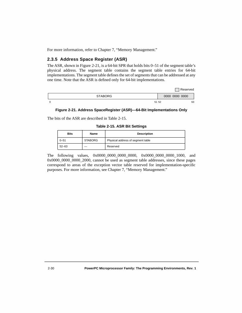
2-30 PowerPC Microprocessor Family: The Programming Environments, Rev. 1
For more information, refer to Chapter 7, “Memory Management.”
2.3.5 Address Space Register (ASR)The ASR, shown in Figure 2-21, is a 64-bit SPR that holds bits 0–51 of the segment table’sphysical address. The segment table contains the segment table entries for 64-bitimplementations. The segment table defines the set of segments that can be addressed at anyone time. Note that the ASR is defined only for 64-bit implementations.
Figure 2-21. Address SpaceRegister (ASR)—64-Bit Implementations Only
The bits of the ASR are described in Table 2-15.
The following values, 0x0000_0000_0000_0000, 0x0000_0000_0000_1000, and0x0000_0000_0000_2000, cannot be used as segment table addresses, since these pagescorrespond to areas of the exception vector table reserved for implementation-specificpurposes. For more information, see Chapter 7, “Memory Management.”
Table 2-15. ASR Bit Settings
Bits Name Description
0–51 STABORG Physical address of segment table
52–63 — Reserved
0 51 52 63
STABORG 0000 0000 0000
Reserved

Chapter 2. PowerPC Register Set 2-31
2.3.6 Segment RegistersThe segment registers contain the segment descriptors for 32-bit implementations. For 32-bit processors, the OEA defines a segment register file of sixteen 32-bit registers. Segmentregisters can be accessed by using the mtsr/mfsr and mtsrin/mfsrin instructions. Thevalue of bit 0, the T bit, determines how the remaining register bits are interpreted.Figure 2-23 shows the format of a segment register when T = 0.
TEMPORARY 64-BIT BRIDGE
Some 64-bit processors implement optional features that simplify the conversion of anoperating system from the 32-bit to the 64-bit portion of the architecture. Thisarchitecturally-defined bridge allows the option of defining bit 63 as ASR[V], theSTABORG field valid bit.
If the ASR[V] bit is implemented and is set, the ASR[STABORG] field is valid andfunctions are as described for the 64-bit architecture. However, if the ASR[V] bit isimplemented and ASR[V] and MSR[SF] are cleared, an operating system can use 16 SLBentries similarly to the way 32-bit implementations use the segment registers, which areotherwise not supported in the 64-bit architecture. Note that if ASR[V] = 0, a reference toa nonexistent address in the STABORG field does not cause a machine check exception.For more information, see Section 7.7.1.1, “Address Space Register (ASR).”
The ASR, with the optional V bit implemented, is shown in Figure 2-22.
Figure 2-22. Address Space Register (ASR)—64-Bit Bridge
The bits of the ASR, including the optional V bit, are described in Table 2-16.
Table 2-16. ASR Bit Settings—64-Bit BridgeBits Name Description
0–51 STABORG Physical address of segment table
52–62 — Reserved
63 V STABORG field valid (V = 1) or invalid (V = 0).Note that the V bit of the ASR is optional. If the function is not implemented, this bit is treated as reserved, except that it is assumed to be set for address translation.
0 51 52 62 63
STABORG 0000 0000 000 V
Reserved

2-32 PowerPC Microprocessor Family: The Programming Environments, Rev. 1
Figure 2-23. Segment Register Format (T = 0)
Segment register bit settings when T = 0 are described in Table 2-17.
Figure 2-24 shows the bit definition when T = 1.
Figure 2-24. Segment Register Format (T = 1)
The bits in the segment register when T = 1 are described in Table 2-18.
Table 2-17. Segment Register Bit Settings (T = 0)
Bits Name Description
0 T T = 0 selects this format
1 Ks Supervisor-state protection key
2 Kp User-state protection key
3 N No-execute protection
4–7 — Reserved
8–31 VSID Virtual segment ID
Table 2-18. Segment Register Bit Settings (T = 1)
Bits Name Description
0 T T = 1 selects this format.
1 Ks Supervisor-state protection key
2 Kp User-state protection key
3–11 BUID Bus unit ID
12–31 CNTLR_SPEC Device-specific data for I/O controller
0 1 2 3 4 7 8 31
T Ks Kp N 0000 VSID
Reserved
T Ks Kp BUID Controller-Specific Information
0 1 2 3 11 12 31

Chapter 2. PowerPC Register Set 2-33
If an access is translated by the block address translation (BAT) mechanism, the BATtranslation takes precedence and the results of translation using segment registers are notused. However, if an access is not translated by a BAT, and T = 0 in the selected segmentregister, the effective address is a reference to a memory-mapped segment. In this case, the52-bit virtual address (VA) is formed by concatenating the following:
• The 24-bit VSID field from the segment register• The 16-bit page index, EA[4–19]• The 12-bit byte offset, EA[20–31]
The VA is then translated to a physical address as described in Section 7.5, “MemorySegment Model.”
If T = 1 in the selected segment register (and the access is not translated by a BAT), theeffective address is a reference to a direct-store segment. No reference is made to the pagetables. However, note that the direct-store facility is being phased out of the architecture andwill not likely be supported in future devices. Thus, all new programs should write a valueof zero to the T bit. For further discussion of address translation when T = 1, seeSection 7.8, “Direct-Store Segment Address Translation.”
2.3.7 Data Address Register (DAR)The DAR is a 64-bit register in 64-bit implementations and a 32-bit register in 32-bitimplementations. The DAR is shown in Figure 2-25.
Figure 2-25. Data Address Register (DAR)
The effective address generated by a memory access instruction is placed in the DAR if theaccess causes an exception (for example, an alignment exception). If the exception occursin a 64-bit implementation operating in 32-bit mode, the high-order 32 bits of the DAR arecleared. For information, see Chapter 6, “Exceptions.”
2.3.8 SPRG0–SPRG3SPRG0–SPRG3 are 64-bit or 32-bit registers, depending on the type of PowerPC processor.They are provided for general operating system use, such as performing a fast state save orfor supporting multiprocessor implementations. The formats of SPRG0–SPRG3 are shownin Figure 2-26.
DAR
0 63

2-34 PowerPC Microprocessor Family: The Programming Environments, Rev. 1
Figure 2-26. SPRG0–SPRG3
Table 2-19 provides a description of conventional uses of SPRG0 through SPRG3.
2.3.9 DSISRThe 32-bit DSISR, shown in Figure 2-27, identifies the cause of DSI and alignmentexceptions.
Figure 2-27. DSISR
For information about bit settings, see Section 6.4.3, “DSI Exception (0x00300),” andSection 6.4.6, “Alignment Exception (0x00600).”
2.3.10 Machine Status Save/Restore Register 0 (SRR0)The SRR0 is a 64-bit register in 64-bit implementations and a 32-bit register in 32-bitimplementations. SRR0 is used to save machine status on exceptions and restore machinestatus when an rfid (or rfi) instruction is executed. It also holds the EA for the instructionthat follows the System Call (sc) instruction. The format of SRR0 is shown in Figure 2-28.For 32-bit implementations, the format of SRR0 is that of the low-order bits (32–63) ofFigure 2-28.
Table 2-19. Conventional Uses of SPRG0–SPRG3
Register Description
SPRG0 Software may load a unique physical address in this register to identify an area of memory reserved for use by the first-level exception handler. This area must be unique for each processor in the system.
SPRG1 This register may be used as a scratch register by the first-level exception handler to save the content of a GPR. That GPR then can be loaded from SPRG0 and used as a base register to save other GPRs to memory.
SPRG2 This register may be used by the operating system as needed.
SPRG3 This register may be used by the operating system as needed.
SPRG0
SPRG1
SPRG2
SPRG3
0 63
DSISR
0 31

Chapter 2. PowerPC Register Set 2-35
Figure 2-28. Machine Status Save/Restore Register 0 (SRR0)
When an exception occurs, SRR0 is set to point to an instruction such that all priorinstructions have completed execution and no subsequent instruction has begun execution.When an rfid (or rfi) instruction is executed, the contents of SRR0 are copied to the nextinstruction address (NIA)—the 64- or 32-bit address of the next instruction to be executed.The instruction addressed by SRR0 may not have completed execution, depending on theexception type. SRR0 addresses either the instruction causing the exception or theimmediately following instruction. The instruction addressed can be determined from theexception type and status bits.
If the exception occurs in 32-bit mode of a 64-bit implementation, the high-order 32 bits ofthe NIA are cleared, NIA[32–61] are set from SRR0[32–61], and the two least significantbits of NIA are cleared.
Note that in some implementations, every instruction fetch performed while MSR[IR] = 1,and every instruction execution requiring address translation when MSR[DR] = 1, maymodify SRR0.
For information on how specific exceptions affect SRR0, refer to the descriptions ofindividual exceptions in Chapter 6, “Exceptions.”
2.3.11 Machine Status Save/Restore Register 1 (SRR1)The SRR1 is a 64-bit register in 64-bit implementations and a 32-bit register in 32-bitimplementations. SRR1 is used to save machine status on exceptions and to restoremachine status when an rfid (or rfi) instruction is executed. The format of SRR1 is shownin Figure 2-29.
Figure 2-29. Machine Status Save/Restore Register 1 (SRR1)
In 64-bit implementations, when an exception occurs, bits 33–36 and 42–47 of SRR1 areloaded with exception-specific information and bits 0, 48–55, 57–59, and 62–63 of MSRare placed into the corresponding bit positions of SRR1. When rfid is executed, MSR[0, 48–55, 57–59, 62–63] are loaded from SRR1[0, 48–55, 57–59, 62–63].
SRR0
0 61 62 63
00
Reserved
SRR1
0 63
2-36 PowerPC Microprocessor Family: The Programming Environments, Rev. 1
For 32-bit implementations, when an exception occurs, bits 1–4 and 10–15 of SRR1 areloaded with exception-specific information and bits 16–23, 25–27, and 30–31 of MSR areplaced into the corresponding bit positions of SRR1.When rfi is executed, MSR[16–23,25–27, 30–31] are loaded from SRR1[16–23, 25–27, 30–31].
The remaining bits of SRR1 are defined as reserved. An implementation may define one ormore of these bits, and in this case, may also cause them to be saved from MSR on anexception and restored to MSR from SRR1 on an rfi.
Note that, in some implementations, every instruction fetch when MSR[IR] = 1, and everyinstruction execution requiring address translation when MSR[DR] = 1, may modify SRR1.
For information on how specific exceptions affect SRR1, refer to the individual exceptionsin Chapter 6, “Exceptions.”
2.3.12 Floating-Point Exception Cause Register (FPECR)The FPECR register may be used to identify the cause of a floating-point exception. Notethat the FPECR is an optional register in the PowerPC architecture and may beimplemented differently (or not at all) in the design of each processor. The user’s manualof a specific processor will describe the functionality of the FPECR, if it is implemented inthat processor.
2.3.13 Time Base Facility (TB)—OEAAs described in Section 2.2, “PowerPC VEA Register Set—Time Base,” the time base (TB)provides a long-period counter driven by an implementation-dependent frequency. TheVEA defines user-level read-only access to the TB. Writing to the TB is reserved forsupervisor-level applications such as operating systems and boot-strap routines. The OEAdefines supervisor-level, write access to the TB.
The TB is a volatile resource and must be initialized during reset. Some implementationsmay initialize the TB with a known value; however, there is no guarantee of automaticinitialization of the TB when the processor is reset. The TB runs continuously at start-up.
For more information on the user-level aspects of the time base, refer to Section 2.2,“PowerPC VEA Register Set—Time Base.”
2.3.13.1 Writing to the Time BaseNote that writing to the TB is reserved for supervisor-level software.
The simplified mnemonics, mttbl and mttbu, write the lower and upper halves of the TB,respectively. The simplified mnemonics listed above are for the mtspr instruction; seeAppendix F, “Simplified Mnemonics,” for more information. The mtspr, mttbl, and mttbuinstructions treat TBL and TBU as separate 32-bit registers; setting one leaves the otherunchanged. It is not possible to write the entire 64-bit time base in a single instruction.

Chapter 2. PowerPC Register Set 2-37
The instructions for writing the time base are not dependent on the implementation ormode. Thus, code written to set the TB on a 32-bit implementation will work correctly ona 64-bit implementation running in either 64- or 32-bit mode.
The TB can be written by a sequence such as:
lwz rx,upper #load 64-bit value forlwz ry,lower # TB into rx and ryli rz,0mttbl rz #force TBL to 0mttbu rx #set TBUmttbl ry #set TBL
Provided that no exceptions occur while the last three instructions are being executed,loading 0 into TBL prevents the possibility of a carry from TBL to TBU while the time baseis being initialized.
For information on reading the time base, refer to Section 2.2.1, “Reading the Time Base.”
2.3.14 Decrementer Register (DEC)The decrementer register (DEC), shown in Figure 2-30, is a 32-bit decrementing counterthat provides a mechanism for causing a decrementer exception after a programmabledelay. The DEC frequency is based on the same implementation-dependent frequency thatdrives the time base.
Figure 2-30. Decrementer Register (DEC)
2.3.14.1 Decrementer OperationThe DEC counts down, causing an exception (unless masked by MSR[EE]) when it passesthrough zero. The DEC satisfies the following requirements:
• The operation of the time base and the DEC are coherent (that is, the counters are driven by the same fundamental time base).
• Loading a GPR from the DEC has no effect on the DEC.
• Storing the contents of a GPR to the DEC replaces the value in the DEC with the value in the GPR.
• Whenever bit 0 of the DEC changes from 0 to 1, a decrementer exception request is signaled. Multiple DEC exception requests may be received before the first exception occurs; however, any additional requests are canceled when the exception occurs for the first request.
• If the DEC is altered by software and the content of bit 0 is changed from 0 to 1, an exception request is signaled.
DEC
0 31
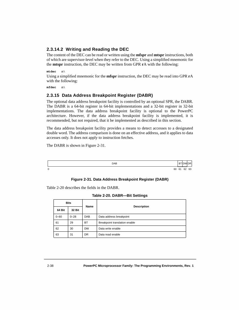
2-38 PowerPC Microprocessor Family: The Programming Environments, Rev. 1
2.3.14.2 Writing and Reading the DECThe content of the DEC can be read or written using the mfspr and mtspr instructions, bothof which are supervisor-level when they refer to the DEC. Using a simplified mnemonic forthe mtspr instruction, the DEC may be written from GPR rA with the following:
mtdec rA
Using a simplified mnemonic for the mfspr instruction, the DEC may be read into GPR rAwith the following:
mfdec rA
2.3.15 Data Address Breakpoint Register (DABR)The optional data address breakpoint facility is controlled by an optional SPR, the DABR.The DABR is a 64-bit register in 64-bit implementations and a 32-bit register in 32-bitimplementations. The data address breakpoint facility is optional to the PowerPCarchitecture. However, if the data address breakpoint facility is implemented, it isrecommended, but not required, that it be implemented as described in this section.
The data address breakpoint facility provides a means to detect accesses to a designateddouble word. The address comparison is done on an effective address, and it applies to dataaccesses only. It does not apply to instruction fetches.
The DABR is shown in Figure 2-31.
Figure 2-31. Data Address Breakpoint Register (DABR)
Table 2-20 describes the fields in the DABR.
Table 2-20. DABR—Bit Settings
BitsName Description
64 Bit 32 Bit
0–60 0–28 DAB Data address breakpoint
61 29 BT Breakpoint translation enable
62 30 DW Data write enable
63 31 DR Data read enable
0 60 61 62 63
DAB BT DW DR

Chapter 2. PowerPC Register Set 2-39
A data address breakpoint match is detected for a load or store instruction if the threefollowing conditions are met for any byte accessed:
• EA[0–60] = DABR[DAB]
• MSR[DR] = DABR[BT]
• The instruction is a store and DABR[DW] = 1, or the instruction is a load and DABR[DR] = 1.
Even if the above conditions are satisfied, it is undefined whether a match occurs in thefollowing cases:
• A store string instruction (stwcx. or stdcx.) in which the store is not performed
• A load or store string instruction (lswx or stswx) with a zero length
• A dcbz, dcbz, eciwx, or ecowx instruction. For the purpose of determining whether a match occurs, eciwx is treated as a load, and dcbz, dcba, and ecowx are treated as stores.
The cache management instructions other than dcbz and dcba never cause a match. If dcbzor dcba causes a match, some or all of the target memory locations may have been updated.
A match generates a DSI exception. Note that in 32-bit mode of a 64-bit implementation,the high-order 32 bits of the EA are treated as zero for the purpose of detecting a match.Refer to Section 6.4.3, “DSI Exception (0x00300),” for more information on the dataaddress breakpoint facility.
2.3.16 External Access Register (EAR)The EAR is an optional 32-bit SPR that controls access to the external control facility andidentifies the target device for external control operations. The external control facilityprovides a means for user-level instructions to communicate with special external devices.The EAR is shown in Figure 2-32.
Figure 2-32. External Access Register (EAR)
The high-order bits of the resource ID (RID) field beyond the width of the RID supportedby a particular implementation are treated as reserved bits.
The EAR register is provided to support the External Control In Word Indexed (eciwx) andExternal Control Out Word Indexed (ecowx) instructions, which are described in Chapter 8,“Instruction Set.” Although access to the EAR is supervisor-level, the operating system candetermine which tasks are allowed to issue external access instructions and when they areallowed to do so. The bit settings for the EAR are described in Table 2-21. Interpretation of
0 1 25 26 31
E 000 0000 0000 0000 0000 0000 00 RID
Reserved

2-40 PowerPC Microprocessor Family: The Programming Environments, Rev. 1
the physical address transmitted by the eciwx and ecowx instructions and the 32-bit valuetransmitted by the ecowx instruction is not prescribed by the PowerPC OEA but isdetermined by the target device. The data access of eciwx and ecowx is performed asthough the memory access mode bits (WIMG) were 0101.
For example, if the external control facility is used to support a graphics adapter, the ecowxinstruction could be used to send the translated physical address of a buffer containinggraphics data to the graphics device. The eciwx instruction could be used to load statusinformation from the graphics adapter.
This register can also be accessed by using the mtspr and mfspr instructions.Synchronization requirements for the EAR are shown in Table 2-22 and Table 2-23.
2.3.17 Processor Identification Register (PIR)The PIR register is used to differentiate between individual processors in a multiprocessorenvironment. Note that the PIR is an optional register in the PowerPC architecture and maybe implemented differently (or not at all) in the design of each processor. The user’s manualof a specific processor will describe the functionality of the PIR, if it is implemented in thatprocessor.
2.3.18 Synchronization Requirements for Special Registers and for Lookaside Buffers
Changing the value in certain system registers, and invalidating SLB and TLB entries, cancause alteration of the context in which data addresses and instruction addresses areinterpreted, and in which instructions are executed. An instruction that alters the context inwhich data addresses or instruction addresses are interpreted, or in which instructions areexecuted, is called a context-altering instruction. The context synchronization required forcontext-altering instructions is shown in Table 2-22 for data access and Table 2-23 forinstruction fetch and execution.
A context-synchronizing exception (that is, any exception except nonrecoverable systemreset or nonrecoverable machine check) can be used instead of a context-synchronizinginstruction. In the tables, if no software synchronization is required before (after) a context-
Table 2-21. External Access Register (EAR) Bit Settings
Bit Name Description
0 E Enable bit 1 Enabled0 DisabledIf this bit is set, the eciwx and ecowx instructions can perform the specified external operation. If the bit is cleared, an eciwx or ecowx instruction causes a DSI exception.
1–25 — Reserved
26–31 RID Resource ID
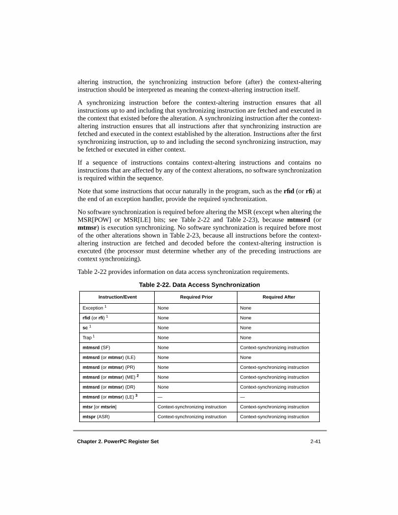
Chapter 2. PowerPC Register Set 2-41
altering instruction, the synchronizing instruction before (after) the context-alteringinstruction should be interpreted as meaning the context-altering instruction itself.
A synchronizing instruction before the context-altering instruction ensures that allinstructions up to and including that synchronizing instruction are fetched and executed inthe context that existed before the alteration. A synchronizing instruction after the context-altering instruction ensures that all instructions after that synchronizing instruction arefetched and executed in the context established by the alteration. Instructions after the firstsynchronizing instruction, up to and including the second synchronizing instruction, maybe fetched or executed in either context.
If a sequence of instructions contains context-altering instructions and contains noinstructions that are affected by any of the context alterations, no software synchronizationis required within the sequence.
Note that some instructions that occur naturally in the program, such as the rfid (or rfi) atthe end of an exception handler, provide the required synchronization.
No software synchronization is required before altering the MSR (except when altering theMSR[POW] or MSR[LE] bits; see Table 2-22 and Table 2-23), because mtmsrd (ormtmsr) is execution synchronizing. No software synchronization is required before mostof the other alterations shown in Table 2-23, because all instructions before the context-altering instruction are fetched and decoded before the context-altering instruction isexecuted (the processor must determine whether any of the preceding instructions arecontext synchronizing).
Table 2-22 provides information on data access synchronization requirements.
Table 2-22. Data Access Synchronization
Instruction/Event Required Prior Required After
Exception 1 None None
rfid (or rfi) 1 None None
sc 1 None None
Trap 1 None None
mtmsrd (SF) None Context-synchronizing instruction
mtmsrd (or mtmsr) (ILE) None None
mtmsrd (or mtmsr) (PR) None Context-synchronizing instruction
mtmsrd (or mtmsr) (ME) 2 None Context-synchronizing instruction
mtmsrd (or mtmsr) (DR) None Context-synchronizing instruction
mtmsrd (or mtmsr) (LE) 3 — —
mtsr [or mtsrin] Context-synchronizing instruction Context-synchronizing instruction
mtspr (ASR) Context-synchronizing instruction Context-synchronizing instruction

2-42 PowerPC Microprocessor Family: The Programming Environments, Rev. 1
For information on instruction access synchronization requirements, see Table 2-23.
1 Synchronization requirements for changing the power conserving mode are implementation-dependent.2 A context synchronizing instruction is required after modification of the MSR[ME] bit to ensure that the
modification takes effect for subsequent machine check exceptions, which may not be recoverable andtherefore may not be context synchronizing.
3 Synchronization requirements for changing from one endian mode to the other are implementation-dependent.4 SDR1 must not be altered when MSR[DR] = 1 or MSR[IR] = 1; if it is, the results are undefined.5 A sync instruction is required before the mtspr instruction because SDR1 identifies the page table and thereby
the location of the referenced and changed (R and C) bits. To ensure that R and C bits are updated in thecorrect page table, SDR1 must not be altered until all R and C bit updates due to instructions before the mtsprhave completed. A sync instruction guarantees this synchronization of R and C bit updates, while neither acontext synchronizing operation nor the instruction fetching mechanism does so.
6 Synchronization requirements for changing the DABR are implementation-dependent.7 For data accesses, the context synchronizing instruction before the slbie, slbia, tlbie, or tlbia instruction
ensures that all memory accesses, due to preceding instructions, have completed to a point at which they havereported all exceptions that may be caused. The context synchronizing instruction after the slbie, slbia, tlbie,or tlbia ensures that subsequent memory accesses will not use the SLB orTLB entry(s) being invalidated. Itdoes not ensure that all memory accesses previously translated by the SLB orTLB entry(s) being invalidatedhave completed with respect to memory or, for tlbie or tlbia, that R and C bit updates associated with thosememory accesses have completed; if these completions must be ensured, the slbie, slbia, tlbie, or tlbia mustbe followed by a sync instruction rather than by a context synchronizing instruction.
8 Multiprocessor systems have other requirements to synchronize TLB invalidate.
mtspr (SDR1) 4, 5 sync Context-synchronizing instruction
mtspr (DBAT) Context-synchronizing instruction Context-synchronizing instruction
mtspr (DABR) 6 — —
mtspr (EAR) Context-synchronizing instruction Context-synchronizing instruction
slbie 7 Context-synchronizing instruction Context-synchronizing instruction or sync
slbia 7 Context-synchronizing instruction Context-synchronizing instruction or sync
tlbie 7, 8 Context-synchronizing instruction Context-synchronizing instruction or sync
tlbia 7, 8 Context-synchronizing instruction Context-synchronizing instruction or sync
Notes:
Table 2-23. Instruction Access Synchronization
Instruction/Event Required Prior Required After
Exception 1 None None
rfid [or rfi] 1 None None
sc 1 None None
Table 2-22. Data Access Synchronization (Continued)
Instruction/Event Required Prior Required After

Chapter 2. PowerPC Register Set 2-43
1 Synchronization requirements for changing the power conserving mode are implementation-dependent.2 The alteration must not cause an implicit branch in effective address space. The mtmsrd (SF) instruction and
all subsequent instructions, up to and including the next context-synchronizing instruction, must have effectiveaddresses that are less than 232.
3 The effect of altering the EE bit is immediate as follows:• If an mtmsrd (or mtmsr) sets the EE bit to 0, neither an external interrupt nor a decrementer exception
can occur after the instruction is executed.• If an mtmsrd (or mtmsr) sets the EE bit to 1 when an external interrupt, decrementer exception, or higher
priority exception exists, the corresponding exception occurs immediately after the mtmsrd (or mtmsr) is executed, and before the next instruction is executed in the program that set MSR[EE].
4 A context synchronizing instruction is required after modification of the MSR[ME] bit to ensure that themodification takes effect for subsequent machine check exceptions, which may not be recoverable and thereforemay not be context synchronizing.
Trap 1 None None
mtmsrd (SF) 2 None Context-synchronizing instruction
mtmsrd (or mtmsr) (POW) 1 — —
mtmsrd (or mtmsr) (ILE) None None
mtmsrd (or mtmsr) (EE) 3 None None
mtmsrd (or mtmsr) (PR) None Context-synchronizing instruction
mtmsrd (or mtmsr) (FP) None Context-synchronizing instruction
mtmsrd (or mtmsr) (ME) 4 None Context-synchronizing instruction
mtmsrd (or mtmsr) (FE0, FE1) None Context-synchronizing instruction
mtmsrd (or mtmsr) (SE, BE) None Context-synchronizing instruction
mtmsrd (or mtmsr) (IP) None None
mtmsrd (or mtmsr) (IR) 5 None Context-synchronizing instruction
mtmsrd (or mtmsr) (RI) None None
mtmsrd (or mtmsr) (LE) 6 — —
mtsr [or mtsrin] 5 None Context-synchronizing instruction
mtspr (ASR) 5 None Context-synchronizing instruction
mtspr (SDR1) 7, 8 sync Context-synchronizing instruction
mtspr (IBAT) 5 None Context-synchronizing instruction
mtspr (DEC) 9 None None
slbie 10 None Context-synchronizing instruction or sync
slbia 10 None Context-synchronizing instruction or sync
tlbie 10, 11 None Context-synchronizing instruction or sync
tlbia 10, 11 None Context-synchronizing instruction or sync
Notes:
Table 2-23. Instruction Access Synchronization (Continued)
Instruction/Event Required Prior Required After

2-44 PowerPC Microprocessor Family: The Programming Environments, Rev. 1
5 The alteration must not cause an implicit branch in physical address space. The physical address of the context-altering instruction and of each subsequent instruction, up to and including the next context synchronizinginstruction, must be independent of whether the alteration has taken effect.
6 Synchronization requirements for changing from one endian mode to the other are implementation-dependent.7 SDR1 must not be altered when MSR[DR] = 1 or MSR[IR] = 1; if it is, the results are undefined.8 A sync instruction is required before the mtspr instruction because SDR1 identifies the page table and thereby
the location of the referenced and changed (R and C) bits. To ensure that R and C bits are updated in the correctpage table, SDR1 must not be altered until all R and C bit updates due to instructions before the mtspr havecompleted. A sync instruction guarantees this synchronization of R and C bit updates, while neither a contextsynchronizing operation nor the instruction fetching mechanism does so.
9 The elapsed time between the content of the decrementer becoming negative and the signaling of thedecrementer exception is not defined.
10 For data accesses, the context synchronizing instruction before the slbie, slbia, tlbie, or tlbia instructionensures that all memory accesses, due to preceding instructions, have completed to a point at which they havereported all exceptions that may be caused. The context synchronizing instruction after the slbie, slbia, tlbie,or tlbia ensures that subsequent memory accesses will not use the SLB or TLB entry(s) being invalidated. Itdoes not ensure that all memory accesses previously translated by the SLB orTLB entry(s) being invalidatedhave completed with respect to memory or, for tlbie or tlbia, that R and C bit updates associated with thosememory accesses have completed; if these completions must be ensured, the slbie, slbia, tlbie, or tlbia mustbe followed by a sync instruction rather than by a context synchronizing instruction.
11 Multiprocessor systems have other requirements to synchronize TLB invalidate.

Chapter 3. Operand Conventions 3-1
Chapter 3 Operand Conventions 3030
This chapter describes the operand conventions as they are represented in two levels of thePowerPC architecture—user instruction set architecture (UISA) and virtual environmentarchitecture (VEA). Detailed descriptions are provided of conventions used for storingvalues in registers and memory, accessing PowerPC registers, and representing data in theseregisters in both big- and little-endian modes. Additionally, the floating-point data formatsand exception conditions are described. Refer to Appendix D, “Floating-Point Models,” formore information on the implementation of the IEEE floating-point execution models.
3.1 Data Organization in Memory and Data TransfersIn a PowerPC microprocessor-based system, bytes in memory are numbered consecutivelystarting with 0. Each number is the address of the corresponding byte. Memory operandsmay be bytes, half words, words, or double words, or, for the load and store multiple andthe load and store string instructions, a sequence of bytes or words. The address of amemory operand is the address of its first byte (that is, of its lowest-numbered byte).Operand length is implicit for each instruction.
The following sections describe the concepts of alignment and byte ordering of data, andtheir significance to the PowerPC architecture.
3.1.1 Aligned and Misaligned AccessesThe operand of a single-register memory access instruction has a natural alignmentboundary equal to the operand length. In other words, the natural address of an operand isan integral multiple of the operand length. A memory operand is said to be aligned if it isaligned at its natural boundary; otherwise it is misaligned. Instructions are always fourbytes long and word-aligned.
U
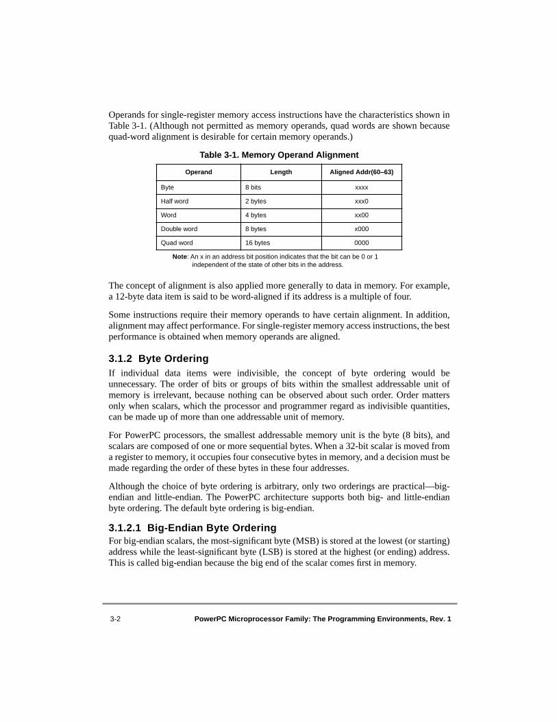
3-2 PowerPC Microprocessor Family: The Programming Environments, Rev. 1
Operands for single-register memory access instructions have the characteristics shown inTable 3-1. (Although not permitted as memory operands, quad words are shown becausequad-word alignment is desirable for certain memory operands.)
The concept of alignment is also applied more generally to data in memory. For example,a 12-byte data item is said to be word-aligned if its address is a multiple of four.
Some instructions require their memory operands to have certain alignment. In addition,alignment may affect performance. For single-register memory access instructions, the bestperformance is obtained when memory operands are aligned.
3.1.2 Byte Ordering If individual data items were indivisible, the concept of byte ordering would beunnecessary. The order of bits or groups of bits within the smallest addressable unit ofmemory is irrelevant, because nothing can be observed about such order. Order mattersonly when scalars, which the processor and programmer regard as indivisible quantities,can be made up of more than one addressable unit of memory.
For PowerPC processors, the smallest addressable memory unit is the byte (8 bits), andscalars are composed of one or more sequential bytes. When a 32-bit scalar is moved froma register to memory, it occupies four consecutive bytes in memory, and a decision must bemade regarding the order of these bytes in these four addresses.
Although the choice of byte ordering is arbitrary, only two orderings are practical—big-endian and little-endian. The PowerPC architecture supports both big- and little-endianbyte ordering. The default byte ordering is big-endian.
3.1.2.1 Big-Endian Byte OrderingFor big-endian scalars, the most-significant byte (MSB) is stored at the lowest (or starting)address while the least-significant byte (LSB) is stored at the highest (or ending) address.This is called big-endian because the big end of the scalar comes first in memory.
Table 3-1. Memory Operand Alignment
Operand Length Aligned Addr(60–63)
Byte 8 bits xxxx
Half word 2 bytes xxx0
Word 4 bytes xx00
Double word 8 bytes x000
Quad word 16 bytes 0000
Note: An x in an address bit position indicates that the bit can be 0 or 1 independent of the state of other bits in the address.
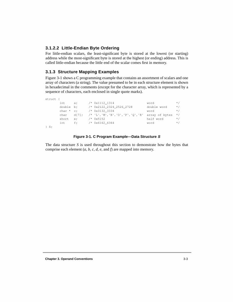
Chapter 3. Operand Conventions 3-3
3.1.2.2 Little-Endian Byte OrderingFor little-endian scalars, the least-significant byte is stored at the lowest (or starting)address while the most-significant byte is stored at the highest (or ending) address. This iscalled little-endian because the little end of the scalar comes first in memory.
3.1.3 Structure Mapping ExamplesFigure 3-1 shows a C programming example that contains an assortment of scalars and onearray of characters (a string). The value presumed to be in each structure element is shownin hexadecimal in the comments (except for the character array, which is represented by asequence of characters, each enclosed in single quote marks).
Figure 3-1. C Program Example—Data Structure S
The data structure S is used throughout this section to demonstrate how the bytes thatcomprise each element (a, b, c, d, e, and f) are mapped into memory.
struct {int a; /* 0x1112_1314 word */double b; /* 0x2122_2324_2526_2728 double word */char * c; /* 0x3132_3334 word */char d[7]; /* 'L','M','N','O','P','Q','R' array of bytes */short e; /* 0x5152 half word */int f; /* 0x6162_6364 word */
} S;

3-4 PowerPC Microprocessor Family: The Programming Environments, Rev. 1
3.1.3.1 Big-Endian MappingThe big-endian mapping of the structure, S, is shown in Figure 3-2. Addresses are shown inhexadecimal below each byte. The content of each byte, as shown in the preceding Cprogramming example, is shown in hexadecimal and, for the character array, as charactersenclosed in single quote marks. Note that the most-significant byte of each scalar is at thelowest address.
Figure 3-2. Big-Endian Mapping of Structure S
The structure mapping introduces padding (skipped bytes indicated by (x) in Figure 3-18)in the map in order to align the scalars on their proper boundaries—four bytes betweenelements a and b, one byte between elements d and e, and two bytes between elements eand f. Note that the padding is dependent on the compiler; it is not a function of thearchitecture.
Contents 11 12 13 14 (x) (x) (x) (x)
Address 00 01 02 03 04 05 06 07
Contents 21 22 23 24 25 26 27 28
Address 08 09 0A 0B 0C 0D 0E 0F
Contents 31 32 33 34 ‘L’ ‘M’ ‘N’ ‘O’
Address 10 11 12 13 14 15 16 17
Contents ‘P’ ‘Q’ ‘R’ (x) 51 52 (x) (x)
Address 18 19 1A 1B 1C 1D 1E 1F
Contents 61 62 63 64 (x) (x) (x) (x)
Address 20 21 22 23 24 25 26 27

Chapter 3. Operand Conventions 3-5
3.1.3.2 Little-Endian MappingFigure 3-3 shows the structure, S, using little-endian mapping. Note that the least-significant byte of each scalar is at the lowest address.
Figure 3-3. Little-Endian Mapping of Structure S
Figure 3-3 shows the sequence of double words laid out with addresses increasing from leftto right. Programmers familiar with little-endian byte ordering may be more accustomed toviewing double words laid out with addresses increasing from right to left, as shown inFigure 3-4. This allows the little-endian programmer to view each scalar in its natural byteorder of MSB to LSB. However, to demonstrate how the PowerPC architecture providesboth big- and little-endian support, this section uses the convention of showing addressesincreasing from left to right, as in Figure 3-3.
Contents 14 13 12 11 (x) (x) (x) (x)
Address 00 01 02 03 04 05 06 07
Contents 28 27 26 25 24 23 22 21
Address 08 09 0A 0B 0C 0D 0E 0F
Contents 34 33 32 31 ‘L’ ‘M’ ‘N’ ‘O’
Address 10 11 12 13 14 15 16 17
Contents ‘P’ ‘Q’ ‘R’ (x) 52 51 (x) (x)
Address 18 19 1A 1B 1C 1D 1E 1F
Contents 64 63 62 61 (x) (x) (x) (x)
Address 20 21 22 23 24 25 26 27
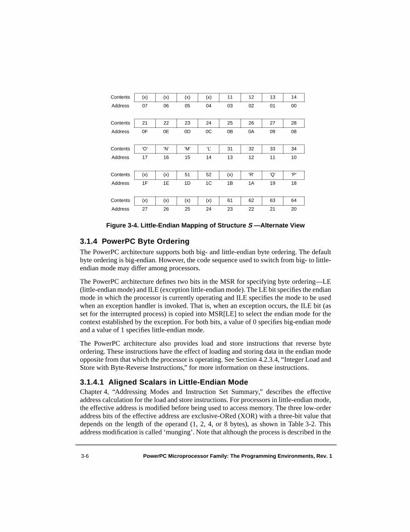
3-6 PowerPC Microprocessor Family: The Programming Environments, Rev. 1
Figure 3-4. Little-Endian Mapping of Structure S —Alternate View
3.1.4 PowerPC Byte OrderingThe PowerPC architecture supports both big- and little-endian byte ordering. The defaultbyte ordering is big-endian. However, the code sequence used to switch from big- to little-endian mode may differ among processors.
The PowerPC architecture defines two bits in the MSR for specifying byte ordering—LE(little-endian mode) and ILE (exception little-endian mode). The LE bit specifies the endianmode in which the processor is currently operating and ILE specifies the mode to be usedwhen an exception handler is invoked. That is, when an exception occurs, the ILE bit (asset for the interrupted process) is copied into MSR[LE] to select the endian mode for thecontext established by the exception. For both bits, a value of 0 specifies big-endian modeand a value of 1 specifies little-endian mode.
The PowerPC architecture also provides load and store instructions that reverse byteordering. These instructions have the effect of loading and storing data in the endian modeopposite from that which the processor is operating. See Section 4.2.3.4, “Integer Load andStore with Byte-Reverse Instructions,” for more information on these instructions.
3.1.4.1 Aligned Scalars in Little-Endian ModeChapter 4, “Addressing Modes and Instruction Set Summary,” describes the effectiveaddress calculation for the load and store instructions. For processors in little-endian mode,the effective address is modified before being used to access memory. The three low-orderaddress bits of the effective address are exclusive-ORed (XOR) with a three-bit value thatdepends on the length of the operand (1, 2, 4, or 8 bytes), as shown in Table 3-2. Thisaddress modification is called ‘munging’. Note that although the process is described in the
Contents (x) (x) (x) (x) 11 12 13 14
Address 07 06 05 04 03 02 01 00
Contents 21 22 23 24 25 26 27 28
Address 0F 0E 0D 0C 0B 0A 09 08
Contents ‘O’ ‘N’ ‘M’ ‘L’ 31 32 33 34
Address 17 16 15 14 13 12 11 10
Contents (x) (x) 51 52 (x) ‘R’ ‘Q’ ‘P’
Address 1F 1E 1D 1C 1B 1A 19 18
Contents (x) (x) (x) (x) 61 62 63 64
Address 27 26 25 24 23 22 21 20

Chapter 3. Operand Conventions 3-7
architecture, the actual term ‘munging’ is not defined or used in the specification. However,the term is commonly used to describe the effective address modifications necessary forconverting big-endian addressed data to little-endian addressed data.
The munged physical address is passed to the cache or to main memory, and the specifiedwidth of the data is transferred (in big-endian order—that is, MSB at the lowest address,LSB at the highest address) between a GPR or FPR and the addressed memory locations(as modified).
Munging makes it appear to the processor that individual aligned scalars are stored as little-endian, when in fact they are stored in big-endian order, but at different byte addresseswithin double words. Only the address is modified, not the byte order.
Taking into account the preceding description of munging, in little-endian mode, structureS is placed in memory as shown in Figure 3-5.
Figure 3-5. Munged Little-Endian Structure S as Seen by the Memory Subsystem
Table 3-2. EA Modifications
Data Width (Bytes) EA Modification
8 No change
4 XOR with 0b100
2 XOR with 0b110
1 XOR with 0b111
Contents (x) (x) (x) (x) 11 12 13 14
Address 00 01 02 03 04 05 06 07
Contents 21 22 23 24 25 26 27 28
Address 08 09 0A 0B 0C 0D 0E 0F
Contents ‘O’ ‘N’ ‘M’ ‘L’ 31 32 33 34
Address 10 11 12 13 14 15 16 17
Contents (x) (x) 51 52 (x) ‘R’ ‘Q’ ‘P’
Address 18 19 1A 1B 1C 1D 1E 1F
Contents (x) (x) (x) (x) 61 62 63 64
Address 20 21 22 23 24 25 26 27

3-8 PowerPC Microprocessor Family: The Programming Environments, Rev. 1
Note that the mapping shown in Figure 3-5 is not a true little-endian mapping of thestructure S. However, because the processor munges the address when accessing memory,the physical structure S shown in Figure 3-5 appears to the processor as the structure Sshown in Figure 3-6.
Figure 3-6. Munged Little-Endian Structure S as Seen by Processor
Note that as seen by the program executing in the processor, the mapping for the structureS (Figure 3-6) is identical to the little-endian mapping shown in Figure 3-3. However, fromoutside of the processor, the addresses of the bytes making up the structure S are as shownin Figure 3-5. These addresses match neither the big-endian mapping of Figure 3-2 nor thetrue little-endian mapping of Figure 3-3. This must be taken into account when performingI/O operations in little-endian mode; this is discussed in Section 3.1.4.5, “PowerPCInput/Output Data Transfer Addressing in Little-Endian Mode.”
Contents 14 13 12 11
Address 00 01 02 03 04 05 06 07
Contents 28 27 26 25 24 23 22 21
Address 08 09 0A 0B 0C 0D 0E 0F
Contents 34 33 32 31 ‘L’ ‘M’ ‘N’ ‘O’
Address 10 11 12 13 14 15 16 17
Contents ‘P’ ‘Q’ ‘R’ 52 51
Address 18 19 1A 1B 1C 1D 1E 1F
Contents 64 63 62 61
Address 20 21 22 23 24 25 26 27

Chapter 3. Operand Conventions 3-9
3.1.4.2 Misaligned Scalars in Little-Endian ModePerforming an XOR operation on the low-order bits of the address works only if the scalaris aligned on a boundary equal to a multiple of its length. Figure 3-7 shows a true little-endian mapping of the four-byte word 0x1112_1314, stored at address 05.
Figure 3-7. True Little-Endian Mapping, Word Stored at Address 05
For the true little-endian example in Figure 3-7, the least-significant byte (0x14) is storedat address 0x05, the next byte (0x13) is stored at address 0x06, the third byte (0x12) isstored at address 0x07, and the most-significant byte (0x11) is stored at address 0x08.
When a PowerPC processor, in little-endian mode, issues a single-register load or storeinstruction with a misaligned effective address, it may take an alignment exception. In thiscase, a single-register load or store instruction means any of the integer load/store,load/store with byte-reverse, memory synchronization (excluding sync), or floating-pointload/store (including stfiwx) instructions. PowerPC processors in little-endian mode are notrequired to invoke an alignment exception when such a misaligned access is attempted. Theprocessor may handle some or all such accesses without taking an alignment exception.
The PowerPC architecture requires that half words, words, and double words be placed inmemory such that the little-endian address of the lowest-order byte is the effective addresscomputed by the load or store instruction; the little-endian address of the next-lowest-orderbyte is one greater, and so on. However, because PowerPC processors in little-endian modemunge the effective address, the order of the bytes of a misaligned scalar must be as if theywere accessed one at a time.
Using the same example as shown in Figure 3-7, when the least-significant byte (0x14) isstored to address 0x05, the address is XORed with 0b111 to become 0x02. When the nextbyte (0x13) is stored to address 0x06, the address is XORed with 0b111 to become 0x01.When the third byte (0x12) is stored to address 0x07, the address is XORed with 0b111 tobecome 0x00. Finally, when the most-significant byte (0x11) is stored to address 0x08, theaddress is XORed with 0b111 to become 0x0F. Figure 3-8 shows the misaligned word,stored by a little-endian program, as seen by the memory subsystem.
Contents 14 13 12
Address 00 01 02 03 04 05 06 07
Contents 11
Address 08 09 0A 0B 0C 0D 0E 0F

3-10 PowerPC Microprocessor Family: The Programming Environments, Rev. 1
Figure 3-8. Word Stored at Little-Endian Address 05 as Seen by the Memory Subsystem
Note that the misaligned word in this example spans two double words. The two parts ofthe misaligned word are not contiguous as seen by the memory system. An implementationmay support some but not all misaligned little-endian accesses. For example, a misalignedlittle-endian access that is contained within a double word may be supported, while one thatspans double words may cause an alignment exception.
3.1.4.3 NonscalarsThe PowerPC architecture has two types of instructions that handle nonscalars (multipleinstances of scalars):
• Load and store multiple instructions• Load and store string instructions
Because these instructions typically operate on more than one word-length scalar, mungingcannot be used. These types of instructions cause alignment exception conditions when theprocessor is executing in little-endian mode. Although string accesses are not supported,they are inherently byte-based operations, and can be broken into a series of word-alignedaccesses.
3.1.4.4 PowerPC Instruction Addressing in Little-Endian ModeEach PowerPC instruction occupies an aligned word of memory. PowerPC processors fetchand execute instructions as if the current instruction address is incremented by four for eachsequential instruction. When operating in little-endian mode, the instruction address ismunged as described in Section 3.1.4.1, “Aligned Scalars in Little-Endian Mode,” forfetching word-length scalars; that is, the instruction address is XORed with 0b100. Aprogram is thus an array of little-endian words with each word fetched and executed inorder (not including branches).
Contents 12 13 14
Address 00 01 02 03 04 05 06 07
Contents 11
Address 08 09 0A 0B 0C 0D 0E 0F

Chapter 3. Operand Conventions 3-11
All instruction addresses visible to an executing program are the effective addresses that arecomputed by that program, or, in the case of the exception handlers, effective addresses thatwere or could have been computed by the interrupted program. These effective addressesare independent of the endian mode. Examples for little-endian mode include thefollowing:
• An instruction address placed in the link register by branch and link operation, or an instruction address saved in an SPR when an exception is taken, is the address that a program executing in little-endian mode would use to access the instruction as a word of data using a load instruction.
• An offset in a relative branch instruction reflects the difference between the addresses of the branch and target instructions, where the addresses used are those that a program executing in little-endian mode would use to access the instructions as data words using a load instruction.
• A target address in an absolute branch instruction is the address that a program executing in little-endian mode would use to access the target instruction as a word of data using a load instruction.
• The memory locations that contain the first set of instructions executed by each kind of exception handler must be set in a manner consistent with the endian mode in which the exception handler is invoked. Thus, if the exception handler is to be invoked in little-endian mode, the first set of instructions comprising each kind of exception handler must appear in memory with the instructions within each double word reversed from the order in which they are to be executed.
3.1.4.5 PowerPC Input/Output Data Transfer Addressing in Little-Endian Mode
For a PowerPC system running in big-endian mode, both the processor and the memorysubsystem recognize the same byte as byte 0. However, this is not true for a PowerPCsystem running in little-endian mode because of the munged address bits when theprocessor accesses memory.
For I/O transfers in little-endian mode to transfer bytes properly, they must be performedas if the bytes transferred were accessed one at a time, using the little-endian addressmodification appropriate for the single-byte transfers (that is, the lowest order address bitsmust be XORed with 0b111). This does not mean that I/O operations in little-endianPowerPC systems must be performed using only one-byte-wide transfers. Data transferscan be as wide as desired, but the order of the bytes within double words must be as if theywere fetched or stored one at a time. That is, for a true little-endian I/O device, the systemmust provide a mechanism to munge and unmunge the addresses and reverse the byteswithin a double word (MSB to LSB).

3-12 PowerPC Microprocessor Family: The Programming Environments, Rev. 1
In earlier processors, I/O operations can also be performed with certain devices by storingto or loading from addresses that are associated with the devices (this is referred to asdirect-store interface operations). However, the direct-store facility is being phased out ofthe architecture and will not likely be supported in future devices. Care must be taken withsuch operations when defining the addresses to be used because these addresses aresubjected to munging as described in Section 3.1.4.1, “Aligned Scalars in Little-EndianMode.” A load or store that maps to a control register on an external device may require thebytes of the value transferred to be reversed. If this reversal is required, the load and storewith byte-reverse instructions may be used. See Section 4.2.3.4, “Integer Load and Storewith Byte-Reverse Instructions,” for more information on these instructions.
3.2 Effect of Operand Placement on Performance—VEA
The PowerPC VEA states that the placement (location and alignment) of operands inmemory affects the relative performance of memory accesses. The best performance isguaranteed if memory operands are aligned on natural boundaries. For more informationon memory access ordering and atomicity, refer to Section 5.1, “The Virtual Environment.”
3.2.1 Summary of Performance EffectsTo obtain the best performance across the widest range of PowerPC processorimplementations, the programmer should assume the performance model described inTable 3-3 and Table 3-4 with respect to the placement of memory operands.
The performance of accesses varies depending on the following:
• Operand size• Operand alignment• Endian mode (big-endian or little-endian)• Crossing no boundary• Crossing a cache block boundary• Crossing a page boundary• Crossing a BAT boundary • Crossing a segment boundary
V

Chapter 3. Operand Conventions 3-13
Table 3-3 applies when the processor is in big-endian mode.
Table 3-3. Performance Effects of Memory Operand Placement, Big-Endian Mode
Table 3-4 applies when the processor is in little-endian mode.
Operand Boundary Crossing
SizeByte
AlignmentNone Cache Block Page BAT/Segment
Integer
8 byte 84<4
OptimalGoodPoor
—GoodPoor
—PoorPoor
—PoorPoor
4 byte 4<4
OptimalGood
—Good
—Poor
—Poor
2 byte 2<2
OptimalGood
—Good
—Poor
—Poor
1 byte 1 Optimal — — —
Imw, stmw 4 Good Good Good1 Poor
String — Good Good Poor Poor
Floating Point None Cache Block Page BAT/Segment
8 byte 84<4
OptimalGoodPoor
—GoodPoor
—PoorPoor
—PoorPoor
4 byte 4<4
OptimalPoor
—Poor
—Poor
—Poor
Note: 1 Note that crossing a page boundary where the memory/cache access attributes of the two pages differ is equivalent to crossing a segment boundary, and thus has poor performance.

3-14 PowerPC Microprocessor Family: The Programming Environments, Rev. 1
Table 3-4. Performance Effects of Memory Operand Placement, Little-Endian Mode
The load/store multiple and the load/store string instructions are supported only in big-endian mode. The load/store multiple instructions are defined by the PowerPC architectureto operate only on aligned operands. The load/store string instructions have no alignmentrequirements.
3.2.2 Instruction RestartIf a memory access crosses a page, BAT, or segment boundary, a number of conditionscould abort the execution of the instruction after part of the access has been performed. Forexample, this may occur when a program attempts to access a page it has not previouslyaccessed or when the processor must check for a possible change in the memory/cacheaccess attributes when an access crosses a page boundary. When this occurs, the processoror the operating system may restart the instruction. If the instruction is restarted, some bytesat that location may be loaded from or stored to the target location a second time.
The following rules apply to memory accesses with regard to restarting the instruction:
• Aligned accesses—A single-register instruction that accesses an aligned operand is never restarted (that is, it is not partially executed).
• Misaligned accesses—A single-register instruction that accesses a misaligned operand may be restarted if the access crosses a page, BAT, or segment boundary, or if the processor is in little-endian mode.
• Load/store multiple, load/store string instructions—These instructions may be restarted if, in accessing the locations specified by the instruction, a page, BAT, or segment boundary is crossed.
Operand Boundary Crossing
SizeByte
AlignmentNone Cache Block Page BAT/Segment
Integer
8 byte 8<8
OptimalPoor
—Poor
—Poor
—Poor
4 byte 4<4
OptimalPoor
—Poor
—Poor
—Poor
2 byte 2<2
OptimalPoor
—Poor
—Poor
—Poor
1 byte 1 Optimal — — —
Floating Point None Cache Block Page BAT/Segment
8 byte 8<8
OptimalPoor
—Poor
—Poor
—Poor
4 byte 4<4
OptimalPoor
—Poor
—Poor
—Poor
Chapter 3. Operand Conventions 3-15
The programmer should assume that any misaligned access in a segment might be restarted.When the processor is in big-endian mode, software can ensure that misaligned accessesare not restarted by placing the misaligned data in BAT areas, as BAT areas have no internalprotection boundaries. Refer to Section 7.4, “Block Address Translation,” for moreinformation on BAT areas.
3.3 Floating-Point Execution Models—UISAThere are two kinds of floating-point instructions defined for the PowerPC architecture:computational and noncomputational. The computational instructions consist of thoseoperations defined by the IEEE-754 standard for 64- and 32-bit arithmetic (those thatperform addition, subtraction, multiplication, division, extracting the square root, roundingconversion, comparison, and combinations of these) and the multiply-add and reciprocalestimate instructions defined by the architecture. The noncomputational floating-pointinstructions consist of the floating-point load, store, and move instructions. While both thecomputational and noncomputational instructions are considered to be floating-pointinstructions governed by the MSR[FP] bit (that allows floating-point instructions to beexecuted), only the computational instructions are considered floating-point operationsthroughout this chapter.
The IEEE standard requires that single-precision arithmetic be provided for single-precision operands. The standard permits double-precision arithmetic instructions to haveeither (or both) single-precision or double-precision operands, but states that single-precision arithmetic instructions should not accept double-precision operands. Theguidelines are as follows:
• Double-precision arithmetic instructions may have single-precision operands but always produce double-precision results.
• Single-precision arithmetic instructions require all operands to be single-precision and always produce single-precision results.
For arithmetic instructions, conversion from double- to single-precision must be doneexplicitly by software, while conversion from single- to double-precision is done implicitlyby the processor.
All PowerPC implementations provide the equivalent of the following execution models toensure that identical results are obtained. The definition of the arithmetic instructions forinfinities, denormalized numbers, and NaNs follow conventions described in the followingsections. Appendix D, “Floating-Point Models,” has additional detailed information on theexecution models for IEEE operations as well as the other floating-point instructions.
Although the double-precision format specifies an 11-bit exponent, exponent arithmeticuses two additional bit positions to avoid potential transient overflow conditions. An extrabit is required when denormalized double-precision numbers are prenormalized. A second
U

3-16 PowerPC Microprocessor Family: The Programming Environments, Rev. 1
bit is required to permit computation of the adjusted exponent value in the followingexamples when the corresponding exception enable bit is 1 (exceptions are referred to asinterrupts in the architecture specification):
• Underflow during multiplication using a denormalized operand• Overflow during division using a denormalized divisor
3.3.1 Floating-Point Data Format The PowerPC UISA defines the representation of a floating-point value in two differentbinary, fixed-length formats. The format is a 32-bit format for a single-precision floating-point value or a 64-bit format for a double-precision floating-point value. The single-precision format may be used for data in memory. The double-precision format can be usedfor data in memory or in floating-point registers (FPRs).
The lengths of the exponent and the fraction fields differ between these two formats. Thelayout of the single-precision format is shown in Figure 3-9; the layout of the double-precision format is shown in Figure 3-10.
Figure 3-9. Floating-Point Single-Precision Format
Figure 3-10. Floating-Point Double-Precision Format
Values in floating-point format consist of three fields:
• S (sign bit)• EXP (exponent + bias)• FRACTION (fraction)
If only a portion of a floating-point data item in memory is accessed, as with a load or storeinstruction for a byte or half word (or word in the case of floating-point double-precisionformat), the value affected depends on whether the PowerPC system is using big- or little-endian byte ordering, which is described in Section 3.1.2, “Byte Ordering.” Big-endianmode is the default.
S EXP FRACTION
0 1 8 9 31
S EXP FRACTION
0 1 11 12 63
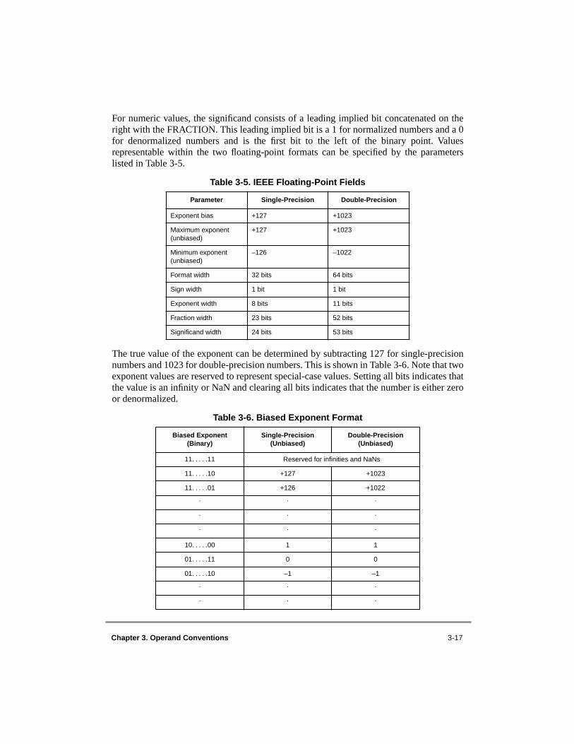
Chapter 3. Operand Conventions 3-17
For numeric values, the significand consists of a leading implied bit concatenated on theright with the FRACTION. This leading implied bit is a 1 for normalized numbers and a 0for denormalized numbers and is the first bit to the left of the binary point. Valuesrepresentable within the two floating-point formats can be specified by the parameterslisted in Table 3-5.
The true value of the exponent can be determined by subtracting 127 for single-precisionnumbers and 1023 for double-precision numbers. This is shown in Table 3-6. Note that twoexponent values are reserved to represent special-case values. Setting all bits indicates thatthe value is an infinity or NaN and clearing all bits indicates that the number is either zeroor denormalized.
Table 3-5. IEEE Floating-Point Fields
Parameter Single-Precision Double-Precision
Exponent bias +127 +1023
Maximum exponent (unbiased)
+127 +1023
Minimum exponent (unbiased)
–126 –1022
Format width 32 bits 64 bits
Sign width 1 bit 1 bit
Exponent width 8 bits 11 bits
Fraction width 23 bits 52 bits
Significand width 24 bits 53 bits
Table 3-6. Biased Exponent Format
Biased Exponent(Binary)
Single-Precision(Unbiased)
Double-Precision(Unbiased)
11. . . . .11 Reserved for infinities and NaNs
11. . . . .10 +127 +1023
11. . . . .01 +126 +1022
. . .
. . .
. . .
10. . . . .00 1 1
01. . . . .11 0 0
01. . . . .10 –1 –1
. . .
. . .

3-18 PowerPC Microprocessor Family: The Programming Environments, Rev. 1
3.3.1.1 Value RepresentationThe PowerPC UISA defines numerical and nonnumerical values representable withinsingle- and double-precision formats. The numerical values are approximations to the realnumbers and include the normalized numbers, denormalized numbers, and zero values. Thenonnumerical values representable are the positive and negative infinities and the NaNs.The positive and negative infinities are adjoined to the real numbers but are not numbersthemselves, and the standard rules of arithmetic do not hold when they appear in anoperation. They are related to the real numbers by order alone. It is possible, however, todefine restricted operations among numbers and infinities as defined below. The relativelocation on the real number line for each of the defined numerical entities is shown inFigure 3-11. Tiny values include denormalized numbers and all numbers that are too smallto be represented for a particular precision format; they do not include ±0.
Figure 3-11. Approximation to Real Numbers
The positive and negative NaNs are encodings that convey diagnostic information such asthe representation of uninitialized variables and are not related to the numbers, ±∞, or eachother by order or value.
Table 3-7 describes each of the floating-point formats.
. . .
00. . . . .01 –126 –1022
00. . . . .00 Reserved for zeros and denormalized numbers
Table 3-7. Recognized Floating-Point Numbers
Sign Bit Biased Exponent Implied Bit Fraction Value
0 Maximum x Nonzero NaN
0 Maximum x Zero +Infinity
0 0 < Exponent < Maximum 1 x +Normalized
0 0 0 Nonzero +Denormalized
0 0 x Zero +0
Table 3-6. Biased Exponent Format (Continued)
Biased Exponent(Binary)
Single-Precision(Unbiased)
Double-Precision(Unbiased)
Tiny Tiny
–∞ –NORM –DENORM +DENORM +NORM +∞
Unrepresentable, small numbers
+0–0

Chapter 3. Operand Conventions 3-19
The following sections describe floating-point values defined in the architecture.
3.3.1.2 Binary Floating-Point NumbersBinary floating-point numbers are machine-representable values used to approximate realnumbers. Three categories of numbers are supported—normalized numbers, denormalizednumbers, and zero values.
3.3.1.3 Normalized Numbers (±NORM)The values for normalized numbers have a biased exponent value in the range:
• 1–254 in single-precision format• 1–2046 in double-precision format
The implied unit bit is one. Normalized numbers are interpreted as follows:
NORM = (–1)s x 2E x (1.fraction)
The variable (s) is the sign, (E) is the unbiased exponent, and (1.fraction) is the significandcomposed of a leading unit bit (implied bit) and a fractional part. The format for normalizednumbers is shown in Figure 3-12.
Figure 3-12. Format for Normalized Numbers
The ranges covered by the magnitude (M) of a normalized floating-point number areapproximated in the following decimal representation:
Single-precision format:
1.2x10–38 ≤ M ≤ 3.4x1038
Double-precision format:
2.2x10–308 ≤ M ≤ 1.8x10308
1 0 x Zero –0
1 0 0 Nonzero –Denormalized
1 0 < Exponent < Maximum 1 x –Normalized
1 Maximum x Zero –Infinity
1 Maximum x Nonzero NaN
Table 3-7. Recognized Floating-Point Numbers (Continued)
Sign Bit Biased Exponent Implied Bit Fraction Value
MIN < EXPONENT < MAX(BIASED) FRACTION = ANY BIT PATTERN
SIGN BIT, 0 OR 1

3-20 PowerPC Microprocessor Family: The Programming Environments, Rev. 1
3.3.1.4 Zero Values (±0)Zero values have a biased exponent value of zero and fraction of zero. This is shown inFigure 3-13. Zeros can have a positive or negative sign. The sign of zero is ignored bycomparison operations (that is, comparison regards +0 as equal to –0). Arithmetic with zeroresults is always exact and does not signal any exception, except when an exception occursdue to the invalid operations as described in Section 3.3.6.1.1, “Invalid OperationException Condition.” Rounding a zero result only affects the sign (±0).
Figure 3-13. Format for Zero Numbers
3.3.1.5 Denormalized Numbers (±DENORM)Denormalized numbers have a biased exponent value of zero and a nonzero fraction. Theformat for denormalized numbers is shown in Figure 3-14.
Figure 3-14. Format for Denormalized Numbers
Denormalized numbers are nonzero numbers smaller in magnitude than the normalizednumbers. They are values in which the implied unit bit is zero. Denormalized numbers areinterpreted as follows:
DENORM = (–1)s x 2Emin x (0.fraction)
The value Emin is the minimum unbiased exponent value for a normalized number (–126for single-precision, –1022 for double-precision).
FRACTION = 0
SIGN BIT, 0 OR 1
EXPONENT = 0(BIASED)
SIGN BIT, 0 OR 1
EXPONENT = 0(BIASED)
FRACTION = ANY NONZEROBIT PATTERN

Chapter 3. Operand Conventions 3-21
3.3.1.6 Infinities (±∞)These are values that have the maximum biased exponent value of 255 in the single-precision format, 2047 in the double-precision format, and a zero fraction value. They areused to approximate values greater in magnitude than the maximum normalized value.Infinity arithmetic is defined as the limiting case of real arithmetic, with restrictedoperations defined among numbers and infinities. Infinities and the real numbers can berelated by ordering in the affine sense:
–∞ < every finite number < +∞
The format for infinities is shown in Figure 3-15.
Figure 3-15. Format for Positive and Negative Infinities
Arithmetic using infinite numbers is always exact and does not signal any exception, exceptwhen an exception occurs due to the invalid operations as described in Section 3.3.6.1.1,“Invalid Operation Exception Condition.”
3.3.1.7 Not a Numbers (NaNs)NaNs have the maximum biased exponent value and a nonzero fraction. The format forNaNs is shown in Figure 3-16. The sign bit of NaN does not show an algebraic sign; rather,it is simply another bit in the NaN. If the highest-order bit of the fraction field is a zero, theNaN is a signaling NaN; otherwise it is a quiet NaN (QNaN).
Figure 3-16. Format for NaNs
Signaling NaNs signal exceptions when they are specified as arithmetic operands.
Quiet NaNs represent the results of certain invalid operations, such as attempts to performarithmetic operations on infinities or NaNs, when the invalid operation exception isdisabled (FPSCR[VE] = 0). Quiet NaNs propagate through all operations, except floating-point round to single-precision, ordered comparison, and conversion to integer operations,and signal exceptions only for ordered comparison and conversion to integer operations.Specific encodings in QNaNs can thus be preserved through a sequence of operations andused to convey diagnostic information to help identify results from invalid operations.
SIGN BIT, 0 OR 1
EXPONENT = MAXIMUM(BIASED) FRACTION = 0
SIGN BIT (ignored)
EXPONENT = MAXIMUM(BIASED)
FRACTION = ANY NONZEROBIT PATTERN

3-22 PowerPC Microprocessor Family: The Programming Environments, Rev. 1
When a QNaN results from an operation because an operand is a NaN or because a QNaNis generated due to a disabled invalid operation exception, the following rule is applied todetermine the QNaN to be stored as the result:
If (frA) is a NaNThen frD ← (frA)Else if (frB) is a NaNThen if instruction is frsp
Then frD ← (frB)[0–34]||(29)0Else frD ← (frB)
Else if (frC) is a NaNThen frD ← (frC)Else if generated QNaN
Then frD ← generated QNaN
If the operand specified by frA is a NaN, that NaN is stored as the result. Otherwise, if theoperand specified by frB is a NaN (if the instruction specifies an frB operand), that NaN isstored as the result, with the low-order 29 bits cleared. Otherwise, if the operand specifiedby frC is a NaN (if the instruction specifies an frC operand), that NaN is stored as the result.Otherwise, if a QNaN is generated by a disabled invalid operation exception, that QNaN isstored as the result. If a QNaN is to be generated as a result, the QNaN generated has a signbit of zero, an exponent field of all ones, and a highest-order fraction bit of one with allother fraction bits zero. An instruction that generates a QNaN as the result of a disabledinvalid operation generates this QNaN. This is shown in Figure 3-17.
Figure 3-17. Representation of Generated QNaN
3.3.2 Sign of ResultThe following rules govern the sign of the result of an arithmetic operation, when theoperation does not yield an exception. These rules apply even when the operands or resultsare ±0 or ±∞:
• The sign of the result of an addition operation is the sign of the source operand having the larger absolute value. If both operands have the same sign, the sign of the result of an addition operation is the same as the sign of the operands. The sign of the result of the subtraction operation, x – y, is the same as the sign of the result of the addition operation, x + (–y).
• When the sum of two operands with opposite sign, or the difference of two operands with the same sign, is exactly zero, the sign of the result is positive in all rounding modes except round toward negative infinity (–∞), in which case the sign is negative.
• The sign of the result of a multiplication or division operation is the XOR of the signs of the source operands.
SIGN BIT (ignored)
111...1 1000....00

Chapter 3. Operand Conventions 3-23
• The sign of the result of a round to single-precision or convert to/from integer operation is the sign of the source operand.
• The sign of the result of a square root or reciprocal square root estimate operation is always positive, except that the square root of –0 is –0 and the reciprocal square root of –0 is –infinity.
For multiply-add instructions, these rules are applied first to the multiplication operationand then to the addition or subtraction operation (one of the source operands to the additionor subtraction operation is the result of the multiplication operation).
3.3.3 Normalization and Denormalization The intermediate result of an arithmetic or Floating Round to Single-Precision (frspx)instruction may require normalization and/or denormalization. When an intermediate resultconsists of a sign bit, an exponent, and a nonzero significand with a zero leading bit, theresult must be normalized (and rounded) before being stored to the target.
A number is normalized by shifting its significand left and decrementing its exponent byone for each bit shifted until the leading significand bit becomes one. The guard and roundbits are also shifted, with zeros shifted into the round bit; see Section D.1, “ExecutionModel for IEEE Operations,” for information about the guard and round bits. Duringnormalization, the exponent is regarded as if its range were unlimited.
If an intermediate result has a nonzero significand and an exponent that is smaller than theminimum value that can be represented in the format specified for the result, this value isreferred to as ‘tiny’ and the stored result is determined by the rules described in Section3.3.6.2.2, “Underflow Exception Condition.” These rules may involve denormalization.The sign of the number does not change.
An exponent can become tiny in either of the following circumstances:
• As the result of an arithmetic or Floating Round to Single-Precision (frspx) instruction or
• As the result of decrementing the exponent in the process of normalization.
Normalization is the process of coercing the leading significand bit to be a 1 whiledenormalization is the process of coercing the exponent into the target format's range. Indenormalization, the significand is shifted to the right while the exponent is incrementedfor each bit shifted until the exponent equals the format’s minimum value. The result is thenrounded. If any significand bits are lost due to the rounding of the shifted value, the resultis considered inexact. The sign of the number does not change.

3-24 PowerPC Microprocessor Family: The Programming Environments, Rev. 1
3.3.4 Data Handling and PrecisionThere are specific instructions for moving floating-point data between the FPRs andmemory. For double-precision format data, the data is not altered during the move. Forsingle-precision data, the format is converted to double-precision format when data isloaded from memory into an FPR. A format conversion from double- to single-precision isperformed when data from an FPR is stored as single-precision. These operations do notcause floating-point exceptions.
All floating-point arithmetic, move, and select instructions use floating-point double-precision format.
Floating-point single-precision formats are obtained by using the following four types ofinstructions:
• Load floating-point single-precision instructions—These instructions access a single-precision operand in single-precision format in memory, convert it to double-precision, and load it into an FPR. Floating-point exceptions do not occur during the load operation.
• Floating Round to Single-Precision (frspx) instruction—The frspx instruction rounds a double-precision operand to single-precision, checking the exponent for single-precision range and handling any exceptions according to respective enable bits in the FPSCR. The instruction places that operand into an FPR as a double-precision operand. For results produced by single-precision arithmetic instructions and by single-precision loads, this operation does not alter the value.
• Single-precision arithmetic instructions—These instructions take operands from the FPRs in double-precision format, perform the operation as if it produced an intermediate result correct to infinite precision and with unbounded range, and then force this intermediate result to fit in single-precision format. Status bits in the FPSCR and in the condition register are set to reflect the single-precision result. The result is then converted to double-precision format and placed into an FPR. The result falls within the range supported by the single-precision format.
Source operands for these instructions must be representable in single-precision format. Otherwise, the result placed into the target FPR and the setting of status bits in the FPSCR, and in the condition register if update mode is selected, are undefined.
• Store floating-point single-precision instructions—These instructions convert a double-precision operand to single-precision format and store that operand into memory. If the operand requires denormalization in order to fit in single-precision format, it is automatically denormalized prior to being stored. No exceptions are detected on the store operation (the value being stored is effectively assumed to be the result of an instruction of one of the preceding three types).
When the result of a Load Floating-Point Single (lfs), Floating Round to Single-Precision(frspx), or single-precision arithmetic instruction is stored in an FPR, the low-order 29fraction bits are zero. This is shown in Figure 3-18.

Chapter 3. Operand Conventions 3-25
Figure 3-18. Single-Precision Representation in an FPR
The frspx instruction allows conversion from double- to single-precision with appropriateexception checking and rounding. This instruction should be used to convert double-precision floating-point values (produced by double-precision load and arithmeticinstructions) to single-precision values before storing them into single-format memoryelements or using them as operands for single-precision arithmetic instructions. Valuesproduced by single-precision load and arithmetic instructions can be stored directly, or useddirectly as operands for single-precision arithmetic instructions, without being preceded byan frspx instruction.
A single-precision value can be used in double-precision arithmetic operations. The reverseis true only if the double-precision value can be represented in single-precision format.Some implementations may execute single-precision arithmetic instructions faster thandouble-precision arithmetic instructions. Therefore, if double-precision accuracy is notrequired, using single-precision data and instructions may speed operations in someimplementations.
3.3.5 RoundingAll arithmetic, rounding, and conversion instructions defined by the PowerPC architecture(except the optional Floating Reciprocal Estimate Single (fresx) and Floating ReciprocalSquare Root Estimate (frsqrtex) instructions) produce an intermediate result considered tobe infinitely precise and with unbounded exponent range. This intermediate result isnormalized or denormalized if required, and then rounded to the destination format. Thefinal result is then placed into the target FPR in the double-precision format or in fixed-pointformat, depending on the instruction.
The IEEE-754 specification allows loss of accuracy to be defined as when the roundedresult differs from the infinitely precise value with unbounded range (same as the definitionof ‘inexact’). In the PowerPC architecture, this is the way loss of accuracy is detected.
Let Z be the intermediate arithmetic result (with infinite precision and unbounded range) orthe operand of a conversion operation. If Z can be represented exactly in the target format,then the result in all rounding modes is exactly Z. If Z cannot be represented exactly in thetarget format, let Z1 and Z2 be the next larger and next smaller numbers representable inthe target format that bound Z; then Z1 or Z2 can be used to approximate the result in thetarget format.
S EXP x x x x . . . . . . . . . . . . . . . . . . . . . . . . . x x x 0 0 0 0 0 . . . . . . . . . . . . . . . . . . . . . . . . . . . . . . . . . . 0 0 0 0
0 1 11 12 63
Bit 35

3-26 PowerPC Microprocessor Family: The Programming Environments, Rev. 1
Figure 3-19 shows a graphical representation of Z, Z1, and Z2 in this case.
Figure 3-19. Relation of Z1 and Z2
Four rounding modes are available through the floating-point rounding control field (RN)in the FPSCR. See Section 2.1.4, “Floating-Point Status and Control Register (FPSCR).”These are encoded as follows in Table 3-8.
See Section D.1, “Execution Model for IEEE Operations,” for a detailed explanation ofrounding. Rounding occurs before an overflow condition is detected. This means that whilean infinitely precise value with unbounded exponent range may be greater than the greatestrepresentable value, the rounding mode may allow that value to be rounded to arepresentable value. In this case, no overflow condition occurs.
Table 3-8. FPSCR Bit Settings—RN Field
RN Rounding Mode Rules
00 Round to nearest Choose the best approximation (Z1 or Z2). In case of a tie, choose the one that is even (least-significant bit 0).
01 Round toward zero Choose the smaller in magnitude (Z1 or Z2).
10 Round toward +infinity Choose Z1.
11 Round toward –infinity Choose Z2.
Negative values
By incrementing lsb of Z
Infinitely precise value
By truncating after lsb
Z2 Z1 0 Z2 Z1
Z ZPositive values
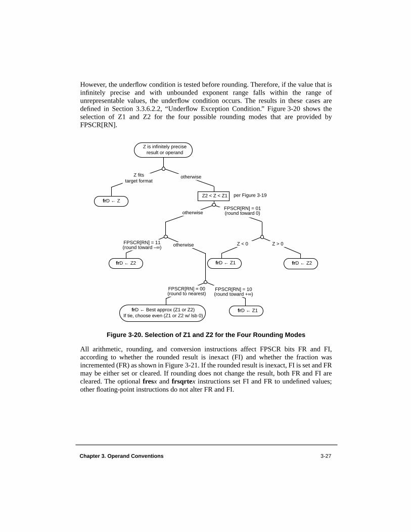
Chapter 3. Operand Conventions 3-27
However, the underflow condition is tested before rounding. Therefore, if the value that isinfinitely precise and with unbounded exponent range falls within the range ofunrepresentable values, the underflow condition occurs. The results in these cases aredefined in Section 3.3.6.2.2, “Underflow Exception Condition.” Figure 3-20 shows theselection of Z1 and Z2 for the four possible rounding modes that are provided byFPSCR[RN].
Figure 3-20. Selection of Z1 and Z2 for the Four Rounding Modes
All arithmetic, rounding, and conversion instructions affect FPSCR bits FR and FI,according to whether the rounded result is inexact (FI) and whether the fraction wasincremented (FR) as shown in Figure 3-21. If the rounded result is inexact, FI is set and FRmay be either set or cleared. If rounding does not change the result, both FR and FI arecleared. The optional fresx and frsqrtex instructions set FI and FR to undefined values;other floating-point instructions do not alter FR and FI.
Z is infinitely precise result or operand
frD ← ZZ2 < Z < Z1 per Figure 3-19
frD ← Z2frD ← Z1frD ← Z2
frD ← Z1frD ← Best approx (Z1 or Z2)If tie, choose even (Z1 or Z2 w/ lsb 0)
Z fits target format
FPSCR[RN] = 01(round toward 0)
Z > 0Z < 0FPSCR[RN] = 11(round toward –∞)
FPSCR[RN] = 00(round to nearest)
FPSCR[RN] = 10(round toward +∞)
otherwise
otherwise
otherwise
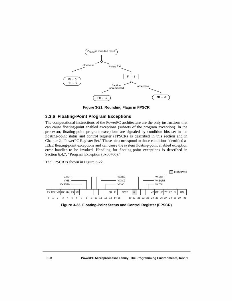
3-28 PowerPC Microprocessor Family: The Programming Environments, Rev. 1
Figure 3-21. Rounding Flags in FPSCR
3.3.6 Floating-Point Program ExceptionsThe computational instructions of the PowerPC architecture are the only instructions thatcan cause floating-point enabled exceptions (subsets of the program exception). In theprocessor, floating-point program exceptions are signaled by condition bits set in thefloating-point status and control register (FPSCR) as described in this section and inChapter 2, “PowerPC Register Set.” These bits correspond to those conditions identified asIEEE floating-point exceptions and can cause the system floating-point enabled exceptionerror handler to be invoked. Handling for floating-point exceptions is described inSection 6.4.7, “Program Exception (0x00700).”
The FPSCR is shown in Figure 3-22.
Figure 3-22. Floating-Point Status and Control Register (FPSCR)
Zround is rounded result
FI ← 0FR ← 0
FI ← 1
FR ← 1 FR ← 0
otherwisefraction incremented
Zround ≠ Zotherwise
0 1 2 3 4 5 6 7 8 9 10 11 12 13 14 15 19 20 21 22 23 24 25 26 27 28 29 30 31
VXIDI
VXISI
VXSNAN
VXZDZ
VXIMZ
VXVC
VXSOFT
VXSQRT
VXCVI
Reserved
FX FEX VX OX UX ZX XX FR FI FPRF 0 VE OE UE ZE XE NI RN
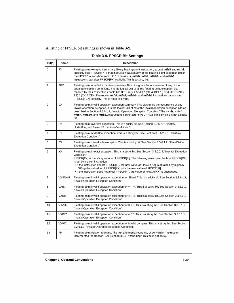
Chapter 3. Operand Conventions 3-29
A listing of FPSCR bit settings is shown in Table 3-9.
Table 3-9. FPSCR Bit Settings
Bit(s) Name Description
0 FX Floating-point exception summary. Every floating-point instruction, except mtfsfi and mtfsf, implicitly sets FPSCR[FX] if that instruction causes any of the floating-point exception bits in the FPSCR to transition from 0 to 1. The mcrfs, mtfsfi, mtfsf, mtfsb0, and mtfsb1 instructions can alter FPSCR[FX] explicitly. This is a sticky bit.
1 FEX Floating-point enabled exception summary. This bit signals the occurrence of any of the enabled exception conditions. It is the logical OR of all the floating-point exception bits masked by their respective enable bits (FEX = (VX & VE) ^ (OX & OE) ^ (UX & UE) ^ (ZX & ZE) ^ (XX & XE)). The mcrfs, mtfsf, mtfsfi, mtfsb0, and mtfsb1 instructions cannot alter FPSCR[FEX] explicitly. This is not a sticky bit.
2 VX Floating-point invalid operation exception summary. This bit signals the occurrence of any invalid operation exception. It is the logical OR of all of the invalid operation exception bits as described in Section 3.3.6.1.1, “Invalid Operation Exception Condition.” The mcrfs, mtfsf, mtfsfi, mtfsb0, and mtfsb1 instructions cannot alter FPSCR[VX] explicitly. This is not a sticky bit.
3 OX Floating-point overflow exception. This is a sticky bit. See Section 3.3.6.2, “Overflow, Underflow, and Inexact Exception Conditions.”
4 UX Floating-point underflow exception. This is a sticky bit. See Section 3.3.6.2.2, “Underflow Exception Condition.”
5 ZX Floating-point zero divide exception. This is a sticky bit. See Section 3.3.6.1.2, “Zero Divide Exception Condition.”
6 XX Floating-point inexact exception. This is a sticky bit. See Section 3.3.6.2.3, “Inexact Exception Condition.” FPSCR[XX] is the sticky version of FPSCR[FI]. The following rules describe how FPSCR[XX] is set by a given instruction:• If the instruction affects FPSCR[FI], the new value of FPSCR[XX] is obtained by logically
ORing the old value of FPSCR[XX] with the new value of FPSCR[FI].• If the instruction does not affect FPSCR[FI], the value of FPSCR[XX] is unchanged.
7 VXSNAN Floating-point invalid operation exception for SNaN. This is a sticky bit. See Section 3.3.6.1.1, “Invalid Operation Exception Condition.”
8 VXISI Floating-point invalid operation exception for ∞ – ∞. This is a sticky bit. See Section 3.3.6.1.1, “Invalid Operation Exception Condition.”
9 VXIDI Floating-point invalid operation exception for ∞ ÷ ∞. This is a sticky bit. See Section 3.3.6.1.1, “Invalid Operation Exception Condition.”
10 VXZDZ Floating-point invalid operation exception for 0 ÷ 0. This is a sticky bit. See Section 3.3.6.1.1, “Invalid Operation Exception Condition.”
11 VXIMZ Floating-point invalid operation exception for ∞ * 0. This is a sticky bit. See Section 3.3.6.1.1, “Invalid Operation Exception Condition.”
12 VXVC Floating-point invalid operation exception for invalid compare. This is a sticky bit. See Section 3.3.6.1.1, “Invalid Operation Exception Condition.”
13 FR Floating-point fraction rounded. The last arithmetic, rounding, or conversion instruction incremented the fraction. See Section 3.3.5, “Rounding.” This bit is not sticky.

3-30 PowerPC Microprocessor Family: The Programming Environments, Rev. 1
14 FI Floating-point fraction inexact. The last arithmetic, rounding, or conversion instruction either produced an inexact result during rounding or caused a disabled overflow exception. See Section 3.3.5, “Rounding.” This is not a sticky bit. For more information regarding the relationship between FPSCR[FI] and FPSCR[XX], see the description of the FPSCR[XX] bit.
15–19 FPRF Floating-point result flags. For arithmetic, rounding, and conversion instructions the field is based on the result placed into the target register, except that if any portion of the result is undefined, the value placed here is undefined. 15 Floating-point result class descriptor (C). Arithmetic, rounding, and conversion
instructions may set this bit with the FPCC bits to indicate the class of the result as shown in Table 3-10.
16–19 Floating-point condition code (FPCC). Floating-point compare instructions always set one of the FPCC bits to one and the other three FPCC bits to zero. Arithmetic, rounding, and conversion instructions may set the FPCC bits with the C bit to indicate the class of the result. Note that in this case the high-order three bits of the FPCC retain their relational significance indicating that the value is less than, greater than, or equal to zero.
16 Floating-point less than or negative (FL or <)17 Floating-point greater than or positive (FG or >)18 Floating-point equal or zero (FE or =)19 Floating-point unordered or NaN (FU or ?)Note that these are not sticky bits.
20 — Reserved
21 VXSOFT Floating-point invalid operation exception for software request. This is a sticky bit. This bit can be altered only by the mcrfs, mtfsfi, mtfsf, mtfsb0, or mtfsb1 instructions. For more detailed information, refer to Section 3.3.6.1.1, “Invalid Operation Exception Condition.”
22 VXSQRT Floating-point invalid operation exception for invalid square root. This is a sticky bit. For more detailed information, refer to Section 3.3.6.1.1, “Invalid Operation Exception Condition.”
23 VXCVI Floating-point invalid operation exception for invalid integer convert. This is a sticky bit. See Section 3.3.6.1.1, “Invalid Operation Exception Condition.”
24 VE Floating-point invalid operation exception enable. See Section 3.3.6.1.1, “Invalid Operation Exception Condition.”
25 OE IEEE floating-point overflow exception enable. See Section 3.3.6.2, “Overflow, Underflow, and Inexact Exception Conditions.”
26 UE IEEE floating-point underflow exception enable. See Section 3.3.6.2.2, “Underflow Exception Condition.”
27 ZE IEEE floating-point zero divide exception enable. See Section 3.3.6.1.2, “Zero Divide Exception Condition.”
28 XE Floating-point inexact exception enable. See Section 3.3.6.2.3, “Inexact Exception Condition.”
Table 3-9. FPSCR Bit Settings (Continued)
Bit(s) Name Description

Chapter 3. Operand Conventions 3-31
Table 3-10 illustrates the floating-point result flags used by PowerPC processors. The resultflags correspond to FPSCR bits 15–19 (the FPRF field).
The following conditions that can cause program exceptions are detected by the processor.These conditions may occur during execution of computational floating-point instructions.The corresponding bits set in the FPSCR are indicated in parentheses:
• Invalid operation exception condition (VX)
— SNaN condition (VXSNAN)— Infinity – infinity condition (VXISI)— Infinity ÷ infinity condition (VXIDI)— Zero ÷ zero condition (VXZDZ)— Infinity * zero condition (VXIMZ)
29 NI Floating-point non-IEEE mode. If this bit is set, results need not conform with IEEE standards and the other FPSCR bits may have meanings other than those described here. If the bit is set and if all implementation-specific requirements are met and if an IEEE-conforming result of a floating-point operation would be a denormalized number, the result produced is zero (retaining the sign of the denormalized number). Any other effects associated with setting this bit are described in the user’s manual for the implementation.Effects of the setting of this bit are implementation-dependent.
30–31 RN Floating-point rounding control. See Section 3.3.5, “Rounding.”00 Round to nearest 01 Round toward zero 10 Round toward +infinity11 Round toward –infinity
Table 3-10. Floating-Point Result Flags — FPSCR[FPRF]
Result Flags (Bits 15–19)Result Value Class
C < > = ?
1 0 0 0 1 Quiet NaN
0 1 0 0 1 –Infinity
0 1 0 0 0 –Normalized number
1 1 0 0 0 –Denormalized number
1 0 0 1 0 –Zero
0 0 0 1 0 +Zero
1 0 1 0 0 +Denormalized number
0 0 1 0 0 +Normalized number
0 0 1 0 1 +Infinity
Table 3-9. FPSCR Bit Settings (Continued)
Bit(s) Name Description
3-32 PowerPC Microprocessor Family: The Programming Environments, Rev. 1
— Invalid compare condition (VXVC)
— Software request condition (VXSOFT)
— Invalid integer convert condition (VXCVI)
— Invalid square root condition (VXSQRT)
These exception conditions are described in Section 3.3.6.1.1, “Invalid Operation Exception Condition.”
• Zero divide exception condition (ZX). These exception conditions are described in Section 3.3.6.1.2, “Zero Divide Exception Condition.”
• Overflow Exception Condition (OX). These exception conditions are described in Section 3.3.6.2.1, “Overflow Exception Condition.”
• Underflow Exception Condition (UX). These exception conditions are described in Section 3.3.6.2.2, “Underflow Exception Condition.”
• Inexact Exception Condition (XX). These exception conditions are described in Section 3.3.6.2.3, “Inexact Exception Condition.”
Each floating-point exception condition and each category of invalid IEEE floating-pointoperation exception condition has a corresponding exception bit in the FPSCR whichindicates the occurrence of that condition. Generally, the occurrence of an exceptioncondition depends only on the instruction and its arguments (with one deviation, describedbelow). When one or more exception conditions arise during the execution of aninstruction, the way in which the instruction completes execution depends on the value ofthe IEEE floating-point enable bits in the FPSCR which govern those exception conditions.If no governing enable bit is set to 1, the instruction delivers a default result. Otherwise,specific condition bits and the FX bit in the FPSCR are set and instruction execution iscompleted by suppressing or delivering a result. Finally, after the instruction execution hascompleted, a nonzero FX bit in the FPSCR causes a program exception if either FE0 or FE1is set in the MSR (invoking the system error handler). The values in the FPRs immediatelyafter the occurrence of an enabled exception do not depend on the FE0 and FE1 bits.
The floating-point exception summary bit (FX) in the FPSCR is set by any floating-pointinstruction (except mtfsfi and mtfsf) that causes any of the exception bits in the FPSCR tochange from 0 to 1, or by mtfsfi, mtfsf, and mtfsb1 instructions that explicitly set one ofthese bits. FPSCR[FEX] is set when any of the exception condition bits is set and theexception is enabled (enable bit is one).
A single instruction may set more than one exception condition bit only in the followingcases:
• The inexact exception condition bit (FPSCR[XX]) may be set with the overflow exception condition bit (FPSCR[OX]).
• The inexact exception condition bit (FPSCR[XX]) may be set with the underflow exception condition bit (FPSCR[UX]).

Chapter 3. Operand Conventions 3-33
• The invalid IEEE floating-point operation exception condition bit (SNaN) may be set with invalid IEEE floating-point operation exception condition bit (∞*0) (FPSCR[VXIMZ]) for multiply-add instructions.
• The invalid operation exception condition bit (SNaN) may be set with the invalid IEEE floating-point operation exception condition bit (invalid compare) (FPRSC[VXVC]) for compare ordered instructions.
• The invalid IEEE floating-point operation exception condition bit (SNaN) may be set with the invalid IEEE floating-point operation exception condition bit (invalid integer convert) (FPSCR[VXCVI]) for convert-to-integer instructions.
Instruction execution is suppressed for the following kinds of exception conditions, so thatthere is no possibility that one of the operands is lost:
• Enabled invalid IEEE floating-point operation• Enabled zero divide
For the remaining kinds of exception conditions, a result is generated and written to thedestination specified by the instruction causing the exception condition. The result maydepend on whether the condition is enabled or disabled. The kinds of exception conditionsthat deliver a result are the following:
• Disabled invalid IEEE floating-point operation• Disabled zero divide• Disabled overflow• Disabled underflow• Disabled inexact• Enabled overflow• Enabled underflow• Enabled inexact
Subsequent sections define each of the floating-point exception conditions and specify theaction taken when they are detected.
The IEEE standard specifies the handling of exception conditions in terms of traps and traphandlers. In the PowerPC architecture, an FPSCR exception enable bit being set causesgeneration of the result value specified in the IEEE standard for the trap enabled case—theexpectation is that the exception is detected by software, which will revise the result. AnFPSCR exception enable bit of 0 causes generation of the default result value specified forthe trap disabled (or no trap occurs or trap is not implemented) case—the expectation is thatthe exception will not be detected by software, which will simply use the default result. Theresult to be delivered in each case for each exception is described in the following sections.

3-34 PowerPC Microprocessor Family: The Programming Environments, Rev. 1
The IEEE default behavior when an exception occurs, which is to generate a default valueand not to notify software, is obtained by clearing all FPSCR exception enable bits andusing ignore exceptions mode (see Table 3-11). In this case the system floating-pointenabled exception error handler is not invoked, even if floating-point exceptions occur. Ifnecessary, software can inspect the FPSCR exception bits to determine whether exceptionshave occurred.
If the system error handler is to be invoked, the corresponding FPSCR exception enable bitmust be set and a mode other than ignore exceptions mode must be used. In this case thesystem floating-point enabled exception error handler is invoked if an enabled floating-point exception condition occurs.
Whether and how the system floating-point enabled exception error handler is invoked if anenabled floating-point exception occurs is controlled by MSR bits FE0 and FE1 as shownin Table 3-11. (The system floating-point enabled exception error handler is never invokedif the appropriate floating-point exception is disabled.)
In precise mode, whenever the system floating-point enabled exception error handler isinvoked, the architecture ensures that all instructions logically residing before the exceptinginstruction have completed and no instruction after the excepting instruction has beenexecuted. In an imprecise mode, the instruction flow may not be interrupted at the point ofthe instruction that caused the exception. The instruction at which the system floating-pointexception handler is invoked has not been executed unless it is the excepting instruction andthe exception is not suppressed.
In either of the imprecise modes, an FPSCR instruction can be used to force the occurrenceof any invocations of the floating-point enabled exception handler, due to instructionsinitiated before the FPSCR instruction. This forcing has no effect in ignore exceptionsmode and is superfluous for precise mode.
Table 3-11. MSR[FE0] and MSR[FE1] Bit Settings for FP Exceptions
FE0 FE1 Description
0 0 Ignore exceptions mode—Floating-point exceptions do not cause the program exception error handler to be invoked.
0 1 Imprecise nonrecoverable mode—When an exception occurs, the exception handler is invoked at some point at or beyond the instruction that caused the exception. It may not be possible to identify the excepting instruction or the data that caused the exception. Results from the excepting instruction may have been used by or affected subsequent instructions executed before the exception handler was invoked.
1 0 Imprecise recoverable mode— When an enabled exception occurs, the floating-point enabled exception handler is invoked at some point at or beyond the instruction that caused the exception. Sufficient information is provided to the exception handler that it can identify the excepting instruction and correct any faulty results. In this mode, no results caused by the excepting instruction have been used by or affected subsequent instructions that are executed before the exception handler is invoked.
1 1 Precise mode—The system floating-point enabled exception error handler is invoked precisely at the instruction that caused the enabled exception.

Chapter 3. Operand Conventions 3-35
Instead of using an FPSCR instruction, an execution synchronizing instruction or event canbe used to force exceptions and set bits in the FPSCR; however, for the best performanceacross the widest range of implementations, an FPSCR instruction should be used toachieve these effects.
For the best performance across the widest range of implementations, the followingguidelines should be considered:
• If IEEE default results are acceptable to the application, FE0 and FE1 should be cleared (ignore exceptions mode). All FPSCR exception enable bits should be cleared.
• If IEEE default results are unacceptable to the application, an imprecise mode should be used with the FPSCR enable bits set as needed.
• Ignore exceptions mode should not, in general, be used when any FPSCR exception enable bits are set.
• Precise mode may degrade performance in some implementations, perhaps substantially, and therefore should be used only for debugging and other specialized applications.
3.3.6.1 Invalid Operation and Zero Divide Exception ConditionsThe flow diagram in Figure 3-23 shows the initial flow for checking floating-pointexception conditions (invalid operation and divide by zero conditions). In any of these casesof floating-point exception conditions, if the FPSCR[FEX] bit is set (implicitly) andMSR[FE0–FE1] ≠ 00, the processor takes a program exception (floating-point enabledexception type). Refer to Chapter 6, “Exceptions,” for more information on exceptionprocessing. The actions performed for each floating-point exception condition aredescribed in greater detail in the following sections.

3-36 PowerPC Microprocessor Family: The Programming Environments, Rev. 1
Figure 3-23. Initial Flow for Floating-Point Exception Conditions
Execute Instruction;x ← Intermediate Result
(Infinitely Precise and with Unbounded Range)
Perform Actions per Section 3.3.6.1.1
Check forFP Exception Conditions
FP Computational Instructions
Invalid Operand Exception Condition
Check for Overflow, Underflow, & Inexact Exception Conditions (see Figure 3-24)
Perform Actions per Section 3.3.6.1.2
• xround ← Rounded x (per FPSCR[RN])• frD ←xround• Set FPSCR[FI, FR, FPRF] appropriately
Continue Instruction Execution
Take FP Enabled Program Exception
Take FP Enabled Program Exception
(for Invalid Operation)
(for Zero Divide)
(FPSCR[FEX] = 1) & (MSR[FE0–FE1] ≠ 00)
x = (0) or (±∞) otherwise
otherwise
otherwiseZero Divide
Exception Condition
otherwise
otherwise
(FPSCR[FEX] = 1) & (MSR[FE0–FE1] ≠ 00)

Chapter 3. Operand Conventions 3-37
3.3.6.1.1 Invalid Operation Exception ConditionAn invalid operation exception occurs when an operand is invalid for the specifiedoperation. The invalid operations are as follows:
• Any operation except load, store, move, select, or mtfsf on a signaling NaN (SNaN)
• For add or subtract operations, magnitude subtraction of infinities (∞ – ∞)
• Division of infinity by infinity (∞ ÷ ∞)
• Division of zero by zero (0 ÷ 0)
• Multiplication of infinity by zero (∞ * 0)
• Ordered comparison involving a NaN (invalid compare)
• Square root or reciprocal square root of a negative, nonzero number (invalid square root). Note that if the implementation does not support the optional floating-point square root or floating-point reciprocal square root estimate instructions, software can simulate the instruction and set the FPSCR[VXSQRT] bit to reflect the exception.
• Integer convert involving a number that is too large in magnitude to be represented in the target format, or involving an infinity or a NaN (invalid integer convert)
FPSCR[VXSOFT] allows software to cause an invalid operation exception for a conditionthat is not necessarily associated with the execution of a floating-point instruction. Forexample, it might be set by a program that computes a square root if the source operand isnegative. This allows PowerPC instructions not implemented in hardware to be emulated.
Any time an invalid operation occurs or software explicitly requests the exception viaFPSCR[VXSOFT], (regardless of the value of FPSCR[VE]), the following actions aretaken:
• One or two invalid operation exception condition bits is setFPSCR[VXSNAN] (if SNaN)FPSCR[VXISI] (if ∞ – ∞)FPSCR[VXIDI] (if ∞ ÷ ∞)FPSCR[VXZDZ] (if 0 ÷ 0)FPSCR[VXIMZ] (if ∞ * 0)FPSCR[VXVC] (if invalid comparison)FPSCR[VXSOFT] (if software request)FPSCR[VXSQRT] (if invalid square root)FPSCR[VXCVI] (if invalid integer convert)
• If the operation is a compare,FPSCR[FR, FI, C] are unchangedFPSCR[FPCC] is set to reflect unordered
• If software explicitly requests the exception,FPSCR[FR, FI, FPRF] are as set by the mtfsfi, mtfsf, or mtfsb1 instruction.
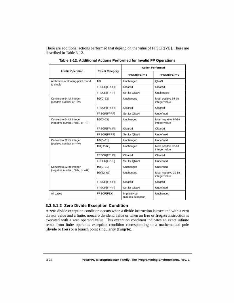
3-38 PowerPC Microprocessor Family: The Programming Environments, Rev. 1
There are additional actions performed that depend on the value of FPSCR[VE]. These aredescribed in Table 3-12.
3.3.6.1.2 Zero Divide Exception ConditionA zero divide exception condition occurs when a divide instruction is executed with a zerodivisor value and a finite, nonzero dividend value or when an fres or frsqrte instruction isexecuted with a zero operand value. This exception condition indicates an exact infiniteresult from finite operands exception condition corresponding to a mathematical pole(divide or fres) or a branch point singularity (frsqrte).
Table 3-12. Additional Actions Performed for Invalid FP Operations
Invalid Operation Result CategoryAction Performed
FPSCR[VE] = 1 FPSCR[VE] = 0
Arithmetic or floating-point round to single
frD Unchanged QNaN
FPSCR[FR, FI] Cleared Cleared
FPSCR[FPRF] Set for QNaN Unchanged
Convert to 64-bit integer (positive number or +∞)
frD[0–63] Unchanged Most positive 64-bit integer value
FPSCR[FR, FI] Cleared Cleared
FPSCR[FPRF] Set for QNaN Undefined
Convert to 64-bit integer (negative number, NaN, or –∞)
frD[0–63] Unchanged Most negative 64-bit integer value
FPSCR[FR, FI] Cleared Cleared
FPSCR[FPRF] Set for QNaN Undefined
Convert to 32-bit integer (positive number or +∞)
frD[0–31] Unchanged Undefined
frD[32–63] Unchanged Most positive 32-bit integer value
FPSCR[FR, FI] Cleared Cleared
FPSCR[FPRF] Set for QNaN Undefined
Convert to 32-bit integer (negative number, NaN, or –∞)
frD[0–31] Unchanged Undefined
frD[32–63] Unchanged Most negative 32-bit integer value
FPSCR[FR, FI] Cleared Cleared
FPSCR[FPRF] Set for QNaN Undefined
All cases FPSCR[FEX] Implicitly set(causes exception)
Unchanged

Chapter 3. Operand Conventions 3-39
When a zero divide condition occurs, the following actions are taken:
• Zero divide exception condition bit is set FPSCR[ZX] = 1.• FPSCR[FR, FI] are cleared.
Additional actions depend on the setting of the zero divide exception condition enable bit,FPSCR[ZE], as described in Table 3-13.
3.3.6.2 Overflow, Underflow, and Inexact Exception ConditionsAs described earlier, the overflow, underflow, and inexact exception conditions are detectedafter the floating-point instruction has executed and an infinitely precise result withunbounded range has been computed. Figure 3-24 shows the flow for the detection of theseconditions and is a continuation of Figure 3-23. As in the cases of invalid operation, or zerodivide conditions, if the FPSCR[FEX] bit is implicitly set as described in Table 3-9 andMSR[FE0–FE1] ≠ 00, the processor takes a program exception (floating-point enabledexception type). Refer to Chapter 6, “Exceptions,” for more information on exceptionprocessing. The actions performed for each of these floating-point exception conditions(including the generated result) are described in greater detail in the following sections.
Table 3-13. Additional Actions Performed for Zero Divide
Result CategoryAction Performed
FPSCR[ZE] = 1 FPSCR[ZE] = 0
frD Unchanged ±∞ (sign determined by XOR of the signs of the operands)
FPSCR[FEX] Implicitly set (causes exception) Unchanged
FPSCR[FPRF] Unchanged Set to indicate ±∞

3-40 PowerPC Microprocessor Family: The Programming Environments, Rev. 1
Figure 3-24. Checking of Remaining Floating-Point Exception Conditions
xnorm ← Normalized x(xnorm Infinitely Precise and with Unbounded Range)
Check for Overflow, Underflow, and Inexact
(from Figure 3-23)
Set FPSCR[FPRF] appropriately
FPSCR[FEX] = 1 (implicitly)
otherwise
If (FPSCR[FEX] = 1) & (MSR[FE0–FE1] ≠ 00), then take FP Program Exception;
otherwise, continue
otherwiseFPSCR[UE] = 0(underflow disabled)
otherwise magnitude of xround > magnitude of largest finite number in result precision
(overflow)
FPSCR[OX] ← 1
otherwise FPSCR[OE] = 0(overflow disabled)
• FPSCR[FEX] = 1 (implicitly)• Adjust Exponent per Table 3-14• frD ← xround (adjusted)• inexact ← xround ≠ xnorm
FPSCR[XX] ← 1
• Get default fromTable 3-15• frD ← default• FPSCR[FI] ← 1• FPSCR[FR] ← undefined
FPSCR[XX] ← 1
otherwise
FPSCR[XE] = 0(inexact disabled)
xround ← Rounded xnorm (per FPSCR[RN])
xnorm is tiny
• xdenorm ← Denormalized xnorm• Round xdenorm (per FPSCR[RN])• frD ← xround ← Rounded xdenorm • inexact ← xround ≠ xdenorm• If ‘inexact’, FPSCR[UX] ← 1
• FPSCR[UX] ← 1• FPSCR[FEX] = 1 (implicitly)• xadjust ←Adj. Exp. of xnorm per Table 3-14• Round xadjust (per FPSCR[RN])• frD ← xround ← Rounded xadjust • inexact ← xround ≠ xadjust
(inexact)
otherwise
• frD ← xround• inexact ← xround ≠ xnorm
inexact = 1

Chapter 3. Operand Conventions 3-41
3.3.6.2.1 Overflow Exception ConditionOverflow occurs when the magnitude of what would have been the rounded result (had theexponent range been unbounded) is greater than the magnitude of the largest finite numberof the specified result precision. Regardless of the setting of the overflow exceptioncondition enable bit of the FPSCR, the following action is taken:
• The overflow exception condition bit is set FPSCR[OX] = 1.
Additional actions are taken that depend on the setting of the overflow exception conditionenable bit of the FPSCR as described in Table 3-14.
Table 3-14. Additional Actions Performed for Overflow Exception Condition
When the overflow exception condition is disabled (FPSCR[OE] = 0) and an overflowcondition occurs, the default result is determined by the rounding mode bit (FPSCR[RN])and the sign of the intermediate result as shown in Table 3-15.
Condition Result CategoryAction Performed
FPSCR[OE] = 1 FPSCR[OE] = 0
Double-precision arithmetic instructions
Exponent of normalized intermediate result
Adjusted by subtracting 1536 —
Single-precision arithmetic and frspx instruction
Exponent of normalized intermediate result
Adjusted by subtracting 192 —
All cases frD Rounded result (with adjusted exponent)
Default result per Table 3-15
FPSCR[XX] Set if rounded result differs from intermediate result
Set
FPSCR[FEX] Implicitly set (causes exception)
Unchanged
FPSCR[FPRF] Set to indicate ±normal number Set to indicate ±∞ or ±normal number
FPSCR[FI] Reflects rounding Set
FPSCR[FR] Reflects rounding Undefined

3-42 PowerPC Microprocessor Family: The Programming Environments, Rev. 1
3.3.6.2.2 Underflow Exception ConditionThe underflow exception condition is defined separately for the enabled and disabled states:
• Enabled—Underflow occurs when the intermediate result is tiny.
• Disabled—Underflow occurs when the intermediate result is tiny and the rounded result is inexact.
In this context, the term ‘tiny’ refers to a floating-point value that is too small to be represented for a particular precision format.
As shown in Figure 3-24, a tiny result is detected before rounding, when a nonzerointermediate result value computed as though it had infinite precision and unboundedexponent range is less in magnitude than the smallest normalized number.
If the intermediate result is tiny and the underflow exception condition enable bit is cleared(FPSCR[UE] = 0), the intermediate result is denormalized (see Section 3.3.3,“Normalization and Denormalization”) and rounded (see Section 3.3.5, “Rounding”)before being stored in an FPR. In this case, if the rounding causes the delivered result valueto differ from what would have been computed were both the exponent range and precisionunbounded (the result is inexact), then underflow occurs and FPSCR[UX] is set.
Table 3-15. Target Result for Overflow Exception Disabled Case
FPSCR[RN]Sign of Intermediate
ResultfrD
Round to nearest Positive +Infinity
Negative –Infinity
Round toward zero Positive Format’s largest finite positive number
Negative Format’s most negative finite number
Round toward +infinity Positive +Infinity
Negative Format’s most negative finite number
Round toward –infinity Positive Format’s largest finite positive number
Negative –Infinity
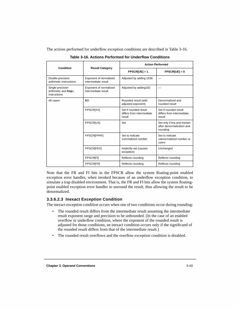
Chapter 3. Operand Conventions 3-43
The actions performed for underflow exception conditions are described in Table 3-16.
Note that the FR and FI bits in the FPSCR allow the system floating-point enabledexception error handler, when invoked because of an underflow exception condition, tosimulate a trap disabled environment. That is, the FR and FI bits allow the system floating-point enabled exception error handler to unround the result, thus allowing the result to bedenormalized.
3.3.6.2.3 Inexact Exception ConditionThe inexact exception condition occurs when one of two conditions occur during rounding:
• The rounded result differs from the intermediate result assuming the intermediate result exponent range and precision to be unbounded. (In the case of an enabled overflow or underflow condition, where the exponent of the rounded result is adjusted for those conditions, an inexact condition occurs only if the significand of the rounded result differs from that of the intermediate result.)
• The rounded result overflows and the overflow exception condition is disabled.
Table 3-16. Actions Performed for Underflow Conditions
Condition Result CategoryAction Performed
FPSCR[UE] = 1 FPSCR[UE] = 0
Double-precision arithmetic instructions
Exponent of normalized intermediate result
Adjusted by adding 1536 —
Single-precision arithmetic and frspx instructions
Exponent of normalized intermediate result
Adjusted by adding192 —
All cases frD Rounded result (with adjusted exponent)
Denormalized and rounded result
FPSCR[XX] Set if rounded result differs from intermediate result
Set if rounded result differs from intermediate result
FPSCR[UX] Set Set only if tiny and inexact after denormalization and rounding
FPSCR[FPRF] Set to indicate ±normalized number
Set to indicate ±denormalized number or ±zero
FPSCR[FEX] Implicitly set (causes exception)
Unchanged
FPSCR[FI] Reflects rounding Reflects rounding
FPSCR[FR] Reflects rounding Reflects rounding

3-44 PowerPC Microprocessor Family: The Programming Environments, Rev. 1
When an inexact exception condition occurs, the following actions are taken independentlyof the setting of the inexact exception condition enable bit of the FPSCR:
• Inexact exception condition bit in the FPSCR is set FPSCR[XX] = 1.• The rounded or overflowed result is placed into the target FPR.• FPSCR[FPRF] is set to indicate the class and sign of the result.
In addition, if the inexact exception condition enable bit in the FPSCR (FPSCR[XE]) is set,and an inexact condition exists, then the FPSCR[FEX] bit is implicitly set, causing theprocessor to take a floating-point enabled program exception.
In PowerPC implementations, running with inexact exception conditions enabled may havegreater latency than enabling other types of floating-point exception conditions.

Chapter 4. Addressing Modes and Instruction Set Summary 4-1
Chapter 4 Addressing Modes and Instruction Set Summary4040
This chapter describes instructions and addressing modes defined by the three levels of thePowerPC architecture—user instruction set architecture (UISA), virtual environmentarchitecture (VEA), and operating environment architecture (OEA). These instructions aredivided into the following functional categories:
• Integer instructions—These include arithmetic and logical instructions. For more information, see Section 4.2.1, “Integer Instructions.”
• Floating-point instructions—These include floating-point arithmetic instructions, as well as instructions that affect the floating-point status and control register (FPSCR). For more information, see Section 4.2.2, “Floating-Point Instructions.”
• Load and store instructions—These include integer and floating-point load and store instructions. For more information, see Section 4.2.3, “Load and Store Instructions.”
• Flow control instructions—These include branching instructions, condition register logical instructions, trap instructions, and other instructions that affect the instruction flow. For more information, see Section 4.2.4, “Branch and Flow Control Instructions.”
• Processor control instructions—These instructions are used for synchronizing memory accesses and managing of caches, TLBs, and the segment registers. For more information, see Section 4.2.5, “Processor Control Instructions—UISA,” Section 4.3.1, “Processor Control Instructions—VEA,” and Section 4.4.2, “Processor Control Instructions—OEA.”
• Memory synchronization instructions—These instructions control the order in which memory operations are completed with respect to asynchronous events, and the order in which memory operations are seen by other processors or memory access mechanisms. For more information, see Section 4.2.6, “Memory Synchronization Instructions—UISA,” and Section 4.3.2, “Memory Synchronization Instructions—VEA.”
• Memory control instructions—These include cache management instructions (user-level and supervisor-level), segment register manipulation instructions, and translation lookaside buffer management instructions. For more information, see Section 4.3.3, “Memory Control Instructions—VEA,” and Section 4.4.3, “Memory
U
V
O

4-2 PowerPC Microprocessor Family: The Programming Environments, Rev. 1
Control Instructions—OEA.” (Note that user-level and supervisor-level are referred to as problem state and privileged state, respectively, in the architecture specification.)
• External control instructions—These instructions allow a user-level program to communicate with a special-purpose device. For more information, see Section 4.3.4, “External Control Instructions.”
This grouping of instructions does not necessarily indicate the execution unit that processesa particular instruction or group of instructions within a processor implementation.
Integer instructions operate on byte, half-word, word, and double-word (in 64-bitimplementations) operands. Floating-point instructions operate on single-precision anddouble-precision floating-point operands. The PowerPC architecture uses instructions thatare four bytes long and word-aligned. It provides for byte, half-word, word, and double-word (in 64-bit implementations) operand fetches and stores between memory and a set of32 general-purpose registers (GPRs). It also provides for word and double-word operandfetches and stores between memory and a set of 32 floating-point registers (FPRs). TheFPRs are 64 bits wide in all PowerPC implementations. The GPRs are 32 bits wide in 32-bit implementations and 64 bits wide in 64-bit implementations.
Arithmetic and logical instructions do not read or modify memory. To use the contents of amemory location in a computation and then modify the same or another memory location,the memory contents must be loaded into a register, modified, and then written to the targetlocation using load and store instructions.
The description of each instruction includes the mnemonic and a formatted list of operands.PowerPC-compliant assemblers support the mnemonics and operand lists. To simplifyassembly language programming, a set of simplified mnemonics (referred to as extendedmnemonics in the architecture specification) and symbols is provided for some of the mostfrequently-used instructions; see Appendix F, “Simplified Mnemonics,” for a complete listof simplified mnemonics.
The instructions are organized by functional categories while maintaining the delineationof the three levels of the PowerPC architecture—UISA, VEA, and OEA; Section 4.2discusses the UISA instructions, followed by Section 4.3 that discusses the VEAinstructions and Section 4.4 that discusses the OEA instructions. See Section 1.1.2, “TheLevels of the PowerPC Architecture,” for more information about the various levels definedby the PowerPC architecture.
4.1 ConventionsThis section describes conventions used for the PowerPC instruction set. Descriptions ofcomputation modes, memory addressing, synchronization, and the PowerPC exceptionsummary follow.
U
U
V
O
U

Chapter 4. Addressing Modes and Instruction Set Summary 4-3
4.1.1 Sequential Execution ModelThe PowerPC processors appear to execute instructions in program order, regardless ofasynchronous events or program exceptions. The execution of a sequence of instructionsmay be interrupted by an exception caused by one of the instructions in the sequence, or byan asynchronous event. (Note that the architecture specification refers to exceptions asinterrupts.)
For exceptions to the sequential execution model, refer to Chapter 6, “Exceptions.” Forinformation about the synchronization required when using store instructions to accessinstruction areas of memory, refer to Section 4.2.3.3, “Integer Store Instructions,” andSection 5.1.5.2, “Instruction Cache Instructions.” For information regarding instructionfetching, and for information about guarded memory refer to Section 5.2.1.5, “TheGuarded Attribute (G).”
4.1.2 Computation ModesThe PowerPC architecture allows for the following types of implementations:
• 64-bit implementations, in which all general-purpose and floating-point registers, and some special-purpose registers (SPRs) are 64 bits long, and effective addresses are 64 bits long. All 64-bit implementations have two modes of operation: 64-bit mode (which is the default) and 32-bit mode. The mode controls how the effective address is interpreted, how condition bits are set, and how the count register (CTR) is tested by branch conditional instructions. All instructions provided for 64-bit implementations are available in both 64- and 32-bit modes.
The machine state register bit 0, MSR[SF], is used to choose between 64- and 32-bit modes. When MSR[SF] = 0, the processor runs in 32-bit mode, and when MSR[SF] = 1 the processor runs in the default 64-bit mode.
• 32-bit implementations, in which all registers except the FPRs are 32 bits long, and effective addresses are 32 bits long.
Instructions defined in this chapter are provided in both 64-bit implementations and 32-bitimplementations unless otherwise stated. Instructions defined only for 64-bitimplementations are illegal in 32-bit implementations, and vice versa.
4.1.2.1 64-Bit ImplementationsIn both 64-bit mode (the default) and 32-bit mode of a 64-bit implementation, instructionsthat set a 64-bit register affect all 64 bits, and the value placed into the register isindependent of mode. In both modes, effective address computations use all 64 bits of therelevant registers (GPRs, LR, CTR, etc.), and produce a 64-bit result; however, in 32-bitmode (MSR[SF] = 0), only the low-order 32 bits of the computed effective address are usedto address memory.
O
U

4-4 PowerPC Microprocessor Family: The Programming Environments, Rev. 1
4.1.2.2 32-Bit ImplementationsFor a 32-bit implementation, all references to 64-bit implementations should bedisregarded. The semantics of instructions for 32-bit implementations are the same as the32-bit mode definitions for 64-bit implementations, except that in a 32-bit implementationall registers except FPRs are 32 bits long.
4.1.3 Classes of InstructionsPowerPC instructions belong to one of the following three classes:
• Defined• Illegal• Reserved
Note that while the definitions of these terms are consistent among the PowerPCprocessors, the assignment of these classifications is not. For example, an instruction thatis specific to 64-bit implementations is considered defined for 64-bit implementations butillegal for 32-bit implementations.
The class is determined by examining the primary opcode, and the extended opcode if any.If the opcode, or the combination of opcode and extended opcode, is not that of a definedinstruction or of a reserved instruction, the instruction is illegal.
In future versions of the PowerPC architecture, instruction codings that are now illegal maybecome defined (by being added to the architecture) or reserved (by being assigned to oneof the special purposes). Likewise, reserved instructions may become defined.
4.1.3.1 Definition of Boundedly UndefinedThe results of executing a given instruction are said to be boundedly undefined if they couldhave been achieved by executing an arbitrary sequence of instructions, starting in the statethe machine was in before executing the given instruction. Boundedly undefined results fora given instruction may vary between implementations, and between different executionson the same implementation.
4.1.3.2 Defined Instruction ClassDefined instructions contain all the instructions defined in the PowerPC UISA, VEA, andOEA. Defined instructions are guaranteed to be supported in all PowerPC implementations.The only exceptions are instructions that are defined only for 64-bit implementations,instructions that are defined only for 32-bit implementations, and optional instructions, asstated in the instruction descriptions in Chapter 8, “Instruction Set.” A PowerPC processormay invoke the illegal instruction error handler (part of the program exception handler)when an unimplemented PowerPC instruction is encountered so that it may be emulated insoftware, as required.
A defined instruction can have invalid forms, as described in Section 4.1.3.2.2, “InvalidInstruction Forms.”
Chapter 4. Addressing Modes and Instruction Set Summary 4-5
4.1.3.2.1 Preferred Instruction FormsA defined instruction may have an instruction form that is preferred (that is, the instructionwill execute in an efficient manner). Any form other than the preferred form will takesignificantly longer to execute. The following instructions have preferred forms:
• Load/store multiple instructions• Load/store string instructions• Or immediate instruction (preferred form of no-op)
4.1.3.2.2 Invalid Instruction FormsA defined instruction may have an instruction form that is invalid if one or more operands,excluding opcodes, are coded incorrectly in a manner that can be deduced by examiningonly the instruction encoding (primary and extended opcodes). Attempting to execute aninvalid form of an instruction either invokes the illegal instruction error handler (a programexception) or yields boundedly-undefined results. See Chapter 8, “Instruction Set,” forindividual instruction descriptions.
Invalid forms result when a bit or operand is coded incorrectly, for example, or when areserved bit (shown as ‘0’) is coded as ‘1’.
The following instructions have invalid forms identified in their individual instructiondescriptions:
• Branch conditional instructions• Load/store with update instructions• Load multiple instructions• Load string instructions• Integer compare instructions (in 32-bit implementations only)• Load/store floating-point with update instructions
4.1.3.2.3 Optional InstructionsA defined instruction may be optional. The optional instructions fall into the followingcategories:
• General-purpose instructions—fsqrt and fsqrts• Graphics instructions—fres, frsqrte, and fsel• External control instructions—eciwx and ecowx• Lookaside buffer management instructions—slbia, slbie, tlbia, tlbie, and tlbsync
(with conditions, see Chapter 8, “Instruction Set,” for more information)
V
O

4-6 PowerPC Microprocessor Family: The Programming Environments, Rev. 1
Note that the stfiwx instruction is defined as optional by the PowerPC architecture to ensurebackwards compatibility with earlier processors; however, it will likely be required forsubsequent PowerPC processors.
Also, note that additional categories may be defined in future implementations. If animplementation claims to support a given category, it implements all the instructions in thatcategory.
Any attempt to execute an optional instruction that is not provided by the implementationwill cause the illegal instruction error handler to be invoked. Exceptions to this rule arestated in the instruction descriptions found in Chapter 8, “Instruction Set.”
4.1.3.3 Illegal Instruction ClassIllegal instructions can be grouped into the following categories:
• Instructions that are not implemented in the PowerPC architecture. These opcodes are available for future extensions of the PowerPC architecture; that is, future versions of the PowerPC architecture may define any of these instructions to perform new functions. The following primary opcodes are defined as illegal but may be used in future extensions to the architecture:
1, 4, 5, 6, 56, 57, 60, 61
• Instructions that are implemented in the PowerPC architecture but are not implemented in a specific PowerPC implementation. For example, instructions specific to 64-bit PowerPC processors are illegal for 32-bit processors.
The following primary opcodes are defined for 64-bit implementations only and areillegal on 32-bit implementations:
2, 30, 58, 62
• All unused extended opcodes are illegal. The unused extended opcodes can be determined from information in Section A.2, “Instructions Sorted by Opcode,” and Section 4.1.3.4, “Reserved Instructions.” Notice that extended opcodes for instructions that are defined only for 64-bit implementations are illegal in 32-bit implementations. The following primary opcodes have unused extended opcodes.
TEMPORARY 64-BIT BRIDGE
The optional 64-bit bridge facility has three other categories of optional instructions for64-bit implementations. These are described in greater detail in Section 7.9, “Migration ofOperating Systems from 32-Bit Implementations to 64-Bit Implementations,” andsummarized below:
• 32-bit segment register support instructions—mtsr, mtsrin, mfsr, and mfsrin • 32-bit system linkage instructions—rfi and mtmsr • 64-bit segment register support instructions—mtsrd and mtsrdin
U
Chapter 4. Addressing Modes and Instruction Set Summary 4-7
19, 31, 59, 63 (primary opcodes 30 and 62 are illegal for 32-bit implementations, butas 64-bit opcodes they have some unused extended opcodes)
• An instruction consisting entirely of zeros is guaranteed to be an illegal instruction. This increases the probability that an attempt to execute data or uninitialized memory invokes the illegal instruction error handler (a program exception). Note that if only the primary opcode consists of all zeros, the instruction is considered a reserved instruction, as described in Section 4.1.3.4, “Reserved Instructions.”
An attempt to execute an illegal instruction invokes the illegal instruction error handler (aprogram exception) but has no other effect. See Section 6.4.7, “Program Exception(0x00700),” for additional information about illegal instruction exception.
With the exception of the instruction consisting entirely of binary zeros, the illegalinstructions are available for further additions to the PowerPC architecture.
4.1.3.4 Reserved InstructionsReserved instructions are allocated to specific implementation-dependent purposes notdefined by the PowerPC architecture. An attempt to execute an unimplemented reservedinstruction invokes the illegal instruction error handler (a program exception). SeeSection 6.4.7, “Program Exception (0x00700),” for additional information about illegalinstruction exception.
The following types of instructions are included in this class:
1. Instructions for the POWER architecture that have not been included in the PowerPC architecture.
2. Implementation-specific instructions used to conform to the PowerPC architecture specifications (for example, Load Data TLB Entry (tlbld) and Load Instruction TLB Entry (tlbli) instructions for the PowerPC 603™ microprocessor).
3. The instruction with primary opcode 0, when the instruction does not consist entirely of binary zeros
4. Any other implementation-specific instructions that are not defined in the UISA, VEA, or OEA
4.1.4 Memory AddressingA program references memory using the effective (logical) address computed by theprocessor when it executes a load, store, branch, or cache instruction, and when it fetchesthe next sequential instruction.
4.1.4.1 Memory OperandsBytes in memory are numbered consecutively starting with zero. Each number is theaddress of the corresponding byte.
U
V
O
U

4-8 PowerPC Microprocessor Family: The Programming Environments, Rev. 1
Memory operands may be bytes, half words, words, or double words, or, for the load/storemultiple and load/store string instructions, a sequence of bytes or words. The address of amemory operand is the address of its first byte (that is, of its lowest-numbered byte).Operand length is implicit for each instruction. The PowerPC architecture supports bothbig-endian and little-endian byte ordering. The default byte and bit ordering is big-endian;see Section 3.1.2, “Byte Ordering,” for more information.
The operand of a single-register memory access instruction has a natural alignmentboundary equal to the operand length. In other words, the “natural” address of an operandis an integral multiple of the operand length. A memory operand is said to be aligned if itis aligned at its natural boundary; otherwise it is misaligned. For a detailed discussion aboutmemory operands, see Chapter 3, “Operand Conventions.”
4.1.4.2 Effective Address CalculationAn effective address (EA) is the 64- or 32-bit sum computed by the processor whenexecuting a memory access or branch instruction or when fetching the next sequentialinstruction. For a memory access instruction, if the sum of the effective address and theoperand length exceeds the maximum effective address, the memory operand is consideredto wrap around from the maximum effective address through effective address 0, asdescribed in the following paragraphs.
Effective address computations for both data and instruction accesses use 64- or 32-bitunsigned binary arithmetic. A carry from bit 0 is ignored. In a 64-bit implementation, the64-bit current instruction address and next instruction address are not affected by a changefrom 32-bit mode to the default 64-bit mode, but a change from the default 64-bit mode to32-bit mode causes the high-order 32 bits to be cleared.
In the default 64-bit mode, the entire 64-bit result comprises the 64-bit effective address.The effective address arithmetic wraps around from the maximum address, 264 – 1, toaddress 0.
When a 64-bit implementation executes in 32-bit mode (MSR[SF] = 0), the low-order 32bits of the 64-bit result comprise the effective address for the purpose of addressingmemory. The high-order 32 bits of the 64-bit effective address are ignored for the purposeof accessing data, but are included whenever a 64-bit effective address is placed into a GPRby load with update and store with update instructions. The high-order 32 bits of the 64-biteffective address are cleared for the purpose of fetching instructions, and whenever a 64-biteffective address is placed into the LR by branch instructions having link register updateoption enabled (LK field, bit 31, in the instruction encoding = 1). The high-order 32 bits ofthe 64-bit effective address are cleared in SPRs when an exception error handler is invoked.In the context of addressing memory, the effective address arithmetic appears to wraparound from the maximum address, 232 – 1, to address zero.
Treating the high-order 32 bits of the effective address as zero effectively truncates the 64-bit effective address to a 32-bit effective address such as would have been generated on a32-bit implementation.
U
O
U
Chapter 4. Addressing Modes and Instruction Set Summary 4-9
In 32-bit implementations, the 32-bit result comprises the 32-bit effective address.
In all implementations (including 32-bit mode in 64-bit implementations), the three low-order bits of the calculated effective address may be modified by the processor beforeaccessing memory if the PowerPC system is operating in little-endian mode. SeeSection 3.1.2, “Byte Ordering,” for more information about little-endian mode.
Load and store operations have three categories of effective address generation that dependon the operands specified:
• Register indirect with immediate index mode• Register indirect with index mode• Register indirect mode
See Section 4.2.3.1, “Integer Load and Store Address Generation,” for a detailed description of effective address generation for load and store operations.
Branch instructions have three categories of effective address generation:
• Immediate addressing.• Link register indirect • Count register indirect
See Section 4.2.4.1, “Branch Instruction Address Calculation,” for a detailed description of effective address generation for branch instructions.
Branch instructions can optionally load the LR with the next sequential instruction address(current instruction address + 4).
4.1.5 Synchronizing InstructionsThe synchronization described in this section refers to the state of activities within theprocessor that is performing the synchronization. Refer to Section 6.1.2,“Synchronization,” for more detailed information about other conditions that can causecontext and execution synchronization.
4.1.5.1 Context Synchronizing InstructionsThe System Call (sc), Return from Interrupt (rfi), Return from Interrupt Double Word(rfid), and Instruction Synchronize (isync) instructions perform context synchronization byallowing previously issued instructions to complete before performing a context switch.Execution of one of these instructions ensures the following:
1. No higher priority exception exists (sc) and instruction dispatching is halted.
2. All previous instructions have completed to a point where they can no longer cause an exception.
If a prior memory access instruction causes one or more direct-store interface error exceptions, the results are guaranteed to be determined before this instruction is executed. However, note that the direct-store facility is being phased out of the architecture and will not likely be supported in future devices.
O
4-10 PowerPC Microprocessor Family: The Programming Environments, Rev. 1
3. Previous instructions complete execution in the context (privilege, protection, and address translation) under which they were issued.
4. The instructions following the sc, rfi, rfid, or isync instruction execute in the context established by these instructions.
4.1.5.2 Execution Synchronizing InstructionsAn instruction is execution synchronizing if it satisfies the conditions of the first two itemsdescribed above for context synchronization. The sync instruction is treated like isync withrespect to the second item described above (that is, the conditions described in the seconditem apply to the completion of sync). The sync and mtmsr instructions are examples ofexecution-synchronizing instructions.
All context-synchronizing instructions are execution-synchronizing. Unlike a contextsynchronizing operation, an execution synchronizing instruction need not ensure that theinstructions following it execute in the context established by that instruction. This newcontext becomes effective sometime after the execution synchronizing instructioncompletes and before or at a subsequent context synchronizing operation.
4.1.6 Exception SummaryPowerPC processors have an exception mechanism for handling system functions and errorconditions in an orderly way. The exception model is defined by the OEA. There are twokinds of exceptions—those caused directly by the execution of an instruction and thosecaused by an asynchronous event. Either may cause components of the system software tobe invoked.
Exceptions can be caused directly by the execution of an instruction as follows:
• An attempt to execute an illegal instruction causes the illegal instruction (program exception) error handler to be invoked. An attempt by a user-level program to execute the supervisor-level instructions listed below causes the privileged instruction (program exception) handler to be invoked.
The PowerPC architecture provides the following supervisor-level instructions: dcbi, mfmsr, mfspr, mfsr, mfsrin, mtmsr, mtmsrd, mtspr, mtsr, mtsrd, mtsrin, mtsrdin, rfi, rfid, slbia, slbie, tlbia, tlbie, and tlbsync (defined by OEA). Note that the privilege level of the mfspr and mtspr instructions depends on the SPR encoding.
• The execution of a defined instruction using an invalid form causes either the illegal instruction error handler or the privileged instruction handler to be invoked.
• The execution of an optional instruction that is not provided by the implementation causes the illegal instruction error handler to be invoked.
• An attempt to access memory in a manner that violates memory protection, or an attempt to access memory that is not available (page fault), causes the DSI exception handler or ISI exception handler to be invoked.
U
U
V
O
U

Chapter 4. Addressing Modes and Instruction Set Summary 4-11
• An attempt to access memory with an effective address alignment that is invalid for the instruction causes the alignment exception handler to be invoked.
• The execution of an sc instruction permits a program to call on the system to perform a service, by causing a system call exception handler to be invoked.
• The execution of a trap instruction invokes the program exception trap handler.
• The execution of a floating-point instruction when floating-point instructions are disabled invokes the floating-point unavailable exception handler.
• The execution of an instruction that causes a floating-point exception that is enabled invokes the floating-point enabled exception handler.
• The execution of a floating-point instruction that requires system software assistance causes the floating-point assist exception handler to be invoked. The conditions under which such software assistance is required are implementation-dependent.
Exceptions caused by asynchronous events are described in Chapter 6, “Exceptions.”
4.2 PowerPC UISA InstructionsThe PowerPC user instruction set architecture (UISA) includes the base user-levelinstruction set (excluding a few user-level cache-control, synchronization, and time baseinstructions), user-level registers, programming model, data types, and addressing modes.This section discusses the instructions defined in the UISA.
4.2.1 Integer InstructionsThe integer instructions consist of the following:
• Integer arithmetic instructions• Integer compare instructions• Integer logical instructions• Integer rotate and shift instructions
Integer instructions use the content of the GPRs as source operands and place results intoGPRs. Integer arithmetic, shift, rotate, and string move instructions may update or readvalues from the XER, and the condition register (CR) fields may be updated if the Rc bit ofthe instruction is set.

4-12 PowerPC Microprocessor Family: The Programming Environments, Rev. 1
These instructions treat the source operands as signed integers unless the instruction isexplicitly identified as performing an unsigned operation. For example, Multiply High-Word Unsigned (mulhwu) and Divide Word Unsigned (divwu) instructions interpret bothoperands as unsigned integers.
The integer instructions that are coded to update the condition register, and the integerarithmetic instruction, addic., set CR bits 0–3 (CR0) to characterize the result of theoperation. In the default 64-bit mode, CR0 is set to reflect a signed comparison of the 64-bit result to zero. In 32-bit mode (of 64-bit implementations), CR0 is set to reflect a signedcomparison of the low-order 32 bits of the result to zero.
The integer arithmetic instructions, addic, addic., subfic, addc, subfc, adde, subfe,addme, subfme, addze, and subfze, always set the XER bit, CA, to reflect the carry out ofbit 0 in the default 64-bit mode and out of bit 32 in 32-bit mode (of 64-bit implementations).Integer arithmetic instructions with the overflow enable (OE) bit set in the instructionencoding (instructions with o suffix) cause the XER[SO] and XER[OV] to reflect anoverflow of the result. Except for the multiply low and divide instructions, these integerarithmetic instructions reflect the overflow of the 64-bit result in the default 64-bit modeand overflow of the low-order 32-bit result in 32-bit mode; however, the multiply low anddivide instructions (mulld, mullw, divd, divw, divdu, and divwu) with o suffix causeXER[SO] and XER[OV] to reflect overflow of the 64-bit result (mulld, divd, and divdu)and overflow of the low-order 32-bit result (mullw, divw, and divwu).
Instructions that select the overflow option (enable XER[OV]) or that set the XER carry bit(CA) may delay the execution of subsequent instructions.
Unless otherwise noted, when CR0 and the XER are set, they reflect the value placed in thetarget register.
4.2.1.1 Integer Arithmetic InstructionsTable 4-1 lists the integer arithmetic instructions for the PowerPC processors.
Table 4-1. Integer Arithmetic Instructions
Name MnemonicOperand Syntax
Operation
Add Immediate addi rD,rA,SIMM The sum (rA|0) + SIMM is placed into rD.
Add Immediate Shifted
addis rD,rA,SIMM The sum (rA|0) + (SIMM || 0x0000) is placed into rD.

Chapter 4. Addressing Modes and Instruction Set Summary 4-13
Add addadd.addoaddo.
rD,rA,rB The sum (rA) + (rB) is placed into rD.
add Addadd. Add with CR Update. The dot suffix enables the update of the
CR.addo Add with Overflow Enabled. The o suffix enables the overflow
bit (OV) in the XER. addo. Add with Overflow and CR Update. The o. suffix enables the
update of the CR and enables the overflow bit (OV) in the XER.
Subtract From subfsubf.subfosubfo.
rD,rA,rB The sum ¬ (rA) + (rB) +1 is placed into rD.
subf Subtract Fromsubf. Subtract from with CR Update. The dot suffix enables the
update of the CR.subfo Subtract from with Overflow Enabled. The o suffix enables the
overflow bit (OV) in the XER.subfo. Subtract from with Overflow and CR Update. The o. suffix
enables the update of the CR and enables the overflow bit (OV) in the XER.
Add Immediate Carrying
addic rD,rA,SIMM The sum (rA) + SIMM is placed into rD.
Add Immediate Carrying and Record
addic. rD,rA,SIMM The sum (rA) + SIMM is placed into rD. The CR is updated.
Subtract from Immediate Carrying
subfic rD,rA,SIMM The sum ¬ (rA) + SIMM + 1 is placed into rD.
Add Carrying addcaddc.addcoaddco.
rD,rA,rB The sum (rA) + (rB) is placed into rD.
addc Add Carryingaddc. Add Carrying with CR Update. The dot suffix enables the
update of the CR.addco Add Carrying with Overflow Enabled. The o suffix enables the
overflow bit (OV) in the XER. addco. Add Carrying with Overflow and CR Update. The o. suffix
enables the update of the CR and enables the overflow bit (OV) in the XER.
Subtract from Carrying
subfcsubfc.subfcosubfco.
rD,rA,rB The sum ¬ (rA) + (rB) + 1 is placed into rD.
subfc Subtract from Carryingsubfc. Subtract from Carrying with CR Update. The dot suffix
enables the update of the CR.subfco Subtract from Carrying with Overflow. The o suffix enables the
overflow bit (OV) in the XER. subfco. Subtract from Carrying with Overflow and CR Update. The o.
suffix enables the update of the CR and enables the overflow bit (OV) in the XER.
Table 4-1. Integer Arithmetic Instructions (Continued)
Name MnemonicOperand Syntax
Operation
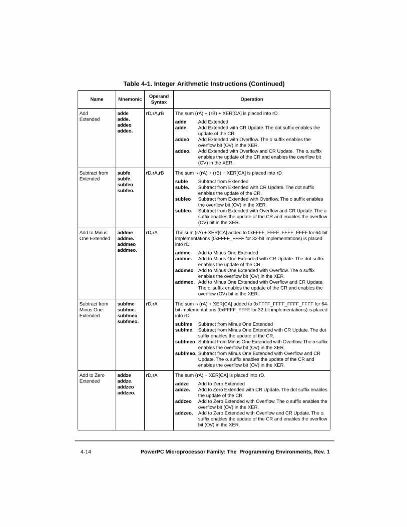
4-14 PowerPC Microprocessor Family: The Programming Environments, Rev. 1
Add Extended
addeadde.addeoaddeo.
rD,rA,rB The sum (rA) + (rB) + XER[CA] is placed into rD.
adde Add Extendedadde. Add Extended with CR Update. The dot suffix enables the
update of the CR. addeo Add Extended with Overflow. The o suffix enables the
overflow bit (OV) in the XER. addeo. Add Extended with Overflow and CR Update. The o. suffix
enables the update of the CR and enables the overflow bit (OV) in the XER.
Subtract from Extended
subfesubfe.subfeosubfeo.
rD,rA,rB The sum ¬ (rA) + (rB) + XER[CA] is placed into rD.
subfe Subtract from Extendedsubfe. Subtract from Extended with CR Update. The dot suffix
enables the update of the CR.subfeo Subtract from Extended with Overflow. The o suffix enables
the overflow bit (OV) in the XER. subfeo. Subtract from Extended with Overflow and CR Update. The o.
suffix enables the update of the CR and enables the overflow (OV) bit in the XER.
Add to Minus One Extended
addmeaddme.addmeoaddmeo.
rD,rA The sum (rA) + XER[CA] added to 0xFFFF_FFFF_FFFF_FFFF for 64-bit implementations (0xFFFF_FFFF for 32-bit implementations) is placed into rD.
addme Add to Minus One Extendedaddme. Add to Minus One Extended with CR Update. The dot suffix
enables the update of the CR.addmeo Add to Minus One Extended with Overflow. The o suffix
enables the overflow bit (OV) in the XER. addmeo. Add to Minus One Extended with Overflow and CR Update.
The o. suffix enables the update of the CR and enables the overflow (OV) bit in the XER.
Subtract from Minus One Extended
subfmesubfme.subfmeosubfmeo.
rD,rA The sum ¬ (rA) + XER[CA] added to 0xFFFF_FFFF_FFFF_FFFF for 64-bit implementations (0xFFFF_FFFF for 32-bit implementations) is placed into rD.
subfme Subtract from Minus One Extendedsubfme. Subtract from Minus One Extended with CR Update. The dot
suffix enables the update of the CR.subfmeo Subtract from Minus One Extended with Overflow. The o suffix
enables the overflow bit (OV) in the XER. subfmeo. Subtract from Minus One Extended with Overflow and CR
Update. The o. suffix enables the update of the CR and enables the overflow bit (OV) in the XER.
Add to Zero Extended
addzeaddze.addzeoaddzeo.
rD,rA The sum (rA) + XER[CA] is placed into rD.
addze Add to Zero Extendedaddze. Add to Zero Extended with CR Update. The dot suffix enables
the update of the CR.addzeo Add to Zero Extended with Overflow. The o suffix enables the
overflow bit (OV) in the XER. addzeo. Add to Zero Extended with Overflow and CR Update. The o.
suffix enables the update of the CR and enables the overflow bit (OV) in the XER.
Table 4-1. Integer Arithmetic Instructions (Continued)
Name MnemonicOperand Syntax
Operation
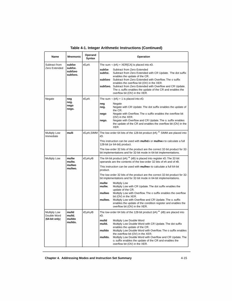
Chapter 4. Addressing Modes and Instruction Set Summary 4-15
Subtract from Zero Extended
subfzesubfze.subfzeosubfzeo.
rD,rA The sum ¬ (rA) + XER[CA] is placed into rD.
subfze Subtract from Zero Extendedsubfze. Subtract from Zero Extended with CR Update. The dot suffix
enables the update of the CR.subfzeo Subtract from Zero Extended with Overflow. The o suffix
enables the overflow bit (OV) in the XER. subfzeo. Subtract from Zero Extended with Overflow and CR Update.
The o. suffix enables the update of the CR and enables the overflow bit (OV) in the XER.
Negate negneg.negonego.
rD,rA The sum ¬ (rA) + 1 is placed into rD.
neg Negateneg. Negate with CR Update. The dot suffix enables the update of
the CR.nego Negate with Overflow. The o suffix enables the overflow bit
(OV) in the XER. nego. Negate with Overflow and CR Update. The o. suffix enables
the update of the CR and enables the overflow bit (OV) in the XER.
Multiply Low Immediate
mulli rD,rA,SIMM The low-order 64 bits of the 128-bit product (rA) ∗ SIMM are placed into rD.
This instruction can be used with mulhdx or mulhwx to calculate a full 128-bit (or 64-bit) product.
The low-order 32 bits of the product are the correct 32-bit product for 32-bit implementations and for 32-bit mode in 64-bit implementations.
Multiply Low mullwmullw.mullwomullwo.
rD,rA,rB The 64-bit product (rA) ∗ (rB) is placed into register rD. The 32-bit operands are the contents of the low-order 32 bits of rA and of rB.
This instruction can be used with mulhwx to calculate a full 64-bit product.
The low-order 32 bits of the product are the correct 32-bit product for 32-bit implementations and for 32-bit mode in 64-bit implementations.
mullw Multiply Low mullw. Multiply Low with CR Update. The dot suffix enables the
update of the CR.mullwo Multiply Low with Overflow. The o suffix enables the overflow
bit (OV) in the XER.mullwo. Multiply Low with Overflow and CR Update. The o. suffix
enables the update of the condition register and enables the overflow bit (OV) in the XER.
Multiply Low Double Word(64-bit only)
mulldmulld.mulldomulldo.
rD,rA,rB The low-order 64 bits of the 128-bit product (rA) ∗ (rB) are placed into rD.
mulld Multiply Low Double Wordmulld. Multiply Low Double Word with CR Update. The dot suffix
enables the update of the CR.mulldo Multiply Low Double Word with Overflow. The o suffix enables
the overflow bit (OV) in the XER.mulldo. Multiply Low Double Word with Overflow and CR Update. The
o. suffix enables the update of the CR and enables the overflow bit (OV) in the XER.
Table 4-1. Integer Arithmetic Instructions (Continued)
Name MnemonicOperand Syntax
Operation

4-16 PowerPC Microprocessor Family: The Programming Environments, Rev. 1
Multiply High Word
mulhwmulhw.
rD,rA,rB The contents of rA and rB are interpreted as 32-bit signed integers. The 64-bit product is formed. The high-order 32 bits of the 64-bit product are placed into the low-order 32 bits of rD. The value in the high-order 32 bits of rD is undefined.
mulhw Multiply High Wordmulhw. Multiply High Word with CR Update. The dot suffix enables
the update of the CR.
Multiply High Double Word(64-bit only)
mulhdmulhd.
rD,rA,rB The high-order 64 bits of the 128-bit product (rA) ∗ ( rB) are placed into register rD. Both operands and the product are interpreted as signed integers.
mulld Multiply High Double Wordmulld. Multiply High Double Word with CR Update. The dot suffix
enables the update of the CR.
Multiply High Word Unsigned
mulhwumulhwu.
rD,rA,rB The contents of rA and of rB are interpreted as 32-bit unsigned integers. The 64-bit product is formed. The high-order 32 bits of the 64-bit product are placed into the low-order 32 bits of rD. The value in the high-order 32 bits of rD is undefined.
mulhwu Multiply High Word Unsignedmulhwu. Multiply High Word Unsigned with CR Update. The dot suffix
enables the update of the CR.
Multiply High Double Word Unsigned(64-bit only)
mulhdumulhdu.
rD,rA,rB The high-order 64 bits of the 128-bit product (rA) ∗ ( rB) are placed into register rD.
mulhdu Multiply High Word Unsignedmulhdu. Multiply High Word Unsigned with CR Update. The dot suffix
enables the update of the CR.
Divide Word divwdivw.divwodivwo.
rD,rA,rB The 64-bit dividend is the signed value of the low-order 32 bits of rA. The 64-bit divisor is the signed value of the low-order 32 bits of rB. The low-order 32 bits of the 64-bit quotient are placed into the low-order 32 bits of rD. The contents of the high-order 32 bits of rD are undefined for 64-bit implementations. The remainder is not supplied as a result.
divw Divide Worddivw. Divide Word with CR Update. The dot suffix enables the update
of the CR.divwo Divide Word with Overflow. The o suffix enables the overflow bit
(OV) in the XER.divwo. Divide Word with Overflow and CR Update. The o. suffix enables
the update of the CR and enables the overflow bit (OV) in the XER.
Divide Double Word(64-bit only)
divddivd.divdodivdo.
rD,rA,rB The 64-bit dividend is (rA). The 64-bit divisor is (rB). The 64-bit quotient is placed into rD. The remainder is not supplied as a result.
divd Divide Double Word divd. Divide Double Word with CR Update. The dot suffix enables
the update of the CR.divdo Divide Double Word with Overflow. The o suffix enables the
overflow bit (OV) in the XER.divdo. Divide Double Word with Overflow and CR Update. The o.
suffix enables the update of the CR and enables the overflow bit (OV) in the XER.
Table 4-1. Integer Arithmetic Instructions (Continued)
Name MnemonicOperand Syntax
Operation

Chapter 4. Addressing Modes and Instruction Set Summary 4-17
Although there is no “Subtract Immediate” instruction, its effect can be achieved by usingan addi instruction with the immediate operand negated. Simplified mnemonics areprovided that include this negation. The subf instructions subtract the second operand (rA)from the third operand (rB). Simplified mnemonics are provided in which the third operandis subtracted from the second operand. See Appendix F, “Simplified Mnemonics,” forexamples.
4.2.1.2 Integer Compare InstructionsThe integer compare instructions algebraically or logically compare the contents of registerrA with either the zero-extended value of the UIMM operand, the sign-extended value ofthe SIMM operand, or the contents of register rB. The comparison is signed for the cmpiand cmp instructions, and unsigned for the cmpli and cmpl instructions. Table 4-2summarizes the integer compare instructions.
For 64-bit implementations, the PowerPC UISA specifies that the value in the L fielddetermines whether the operands are treated as 32- or 64-bit values. If the L field is 0 theoperand length is 32 bits, and if it is 1 the operand length is 64 bits. The simplifiedmnemonics for integer compare instructions, as shown in Appendix F, “SimplifiedMnemonics,” correctly set or clear the L value in the instruction encoding rather thanrequiring it to be coded as a numeric operand.
Divide Word Unsigned
divwudivwu.divwuodivwuo.
rD,rA,rB The 64-bit dividend is the zero-extended value in the low-order 32 bits of rA. The 64-bit divisor is the zero-extended value in the low-order 32 bits of rB. The low-order 32 bits of the 64-bit quotient are placed into the low-order 32 bits of rD. The contents of the high-order 32 bits of rD are undefined for 64-bit implementations. The remainder is not supplied as a result.
divwu Divide Word Unsigneddivwu. Divide Word Unsigned with CR Update. The dot suffix enables
the update of the CR.divwuo Divide Word Unsigned with Overflow. The o suffix enables the
overflow bit (OV) in the XER.divwuo. Divide Word Unsigned with Overflow and CR Update. The o.
suffix enables the update of the CR and enables the overflow bit (OV) in the XER.
Divide Double Word Unsigned(64-bit only)
divdudivdu.divduodivduo.
rD,rA,rB The 64-bit dividend is (rA). The 64-bit divisor is (rB). The 64-bit quotient is placed into rD. The remainder is not supplied as a result.
divdu Divide Word Unsigneddivdu. Divide Word Unsigned with CR Update. The dot suffix enables
the update of the CR.divduo Divide Word Unsigned with Overflow. The o suffix enables the
overflow bit (OV) in the XER.divduo. Divide Word Unsigned with Overflow and CR Update. The o.
suffix enables the update of the CR and enables the overflow bit (OV) in the XER.
Table 4-1. Integer Arithmetic Instructions (Continued)
Name MnemonicOperand Syntax
Operation

4-18 PowerPC Microprocessor Family: The Programming Environments, Rev. 1
When operands are treated as 32-bit signed quantities, bit 32 of (rA) and (rB) is the signbit. For 32-bit implementations, the L field must be cleared, otherwise the instruction formis invalid.
The integer compare instructions (shown in Table 4-2) set one of the leftmost three bits ofthe designated CR field, and clear the other two. XER[SO] is copied into bit 3 of the CRfield.
The crfD operand can be omitted if the result of the comparison is to be placed in CR0.Otherwise the target CR field must be specified in the instruction crfD field, using anexplicit field number.
For information on simplified mnemonics for the integer compare instructions seeAppendix F, “Simplified Mnemonics.”
4.2.1.3 Integer Logical InstructionsThe logical instructions shown in Table 4-3 perform bit-parallel operations on 64-bitoperands. Logical instructions with the CR updating enabled (uses dot suffix) andinstructions andi. and andis. set CR field CR0 (bits 0 to 2) to characterize the result of thelogical operation. In the default 64-bit mode, these fields are set as if the 64-bit result werecompared algebraically to zero. In 32-bit mode of a 64-bit implementation, these fields areset as if the sign-extended low-order 32 bits of the result were algebraically compared tozero. Logical instructions without CR update and the remaining logical instructions do notmodify the CR. Logical instructions do not affect the XER[SO], XER[OV], and XER[CA]bits.
Table 4-2. Integer Compare Instructions
Name Mnemonic Operand Syntax Operation
Compare Immediate
cmpi crfD,L,rA,SIMM The value in register rA (rA[32–63] sign-extended to 64 bits if L = 0) is compared with the sign-extended value of the SIMM operand, treating the operands as signed integers. The result of the comparison is placed into the CR field specified by operand crfD.
Compare cmp crfD,L,rA,rB The value in register rA (rA[32–63] if L = 0) is compared with the value in register rB (rB[32–63] if L = 0), treating the operands as signed integers. The result of the comparison is placed into the CR field specified by operand crfD.
Compare Logical Immediate
cmpli crfD,L,rA,UIMM The value in register rA (rA[32–63] zero-extended to 64 bits if L = 0) is compared with 0x0000_0000_0000 || UIMM, treating the operands as unsigned integers. The result of the comparison is placed into the CR field specified by operand crfD.
Compare Logical
cmpl crfD,L,rA,rB The value in register rA (rA[32–63] if L = 0) is compared with the value in register rB (rB[32–63] if L = 0), treating the operands as unsigned integers. The result of the comparison is placed into the CR field specified by operand crfD.

Chapter 4. Addressing Modes and Instruction Set Summary 4-19
See Appendix F, “Simplified Mnemonics,” for simplified mnemonic examples for integerlogical operations.
Table 4-3. Integer Logical Instructions
Name MnemonicOperand Syntax
Operation
AND Immediate
andi. rA,rS,UIMM The contents of rS are ANDed with 0x0000_0000_0000 || UIMM and the result is placed into rA.The CR is updated.
AND ImmediateShifted
andis. rA,rS,UIMM The content of rS are ANDed with 0x0000_0000 || UIMM || 0x0000 and the result is placed into rA.The CR is updated.
OR Immediate
ori rA,rS,UIMM The contents of rS are ORed with 0x0000_0000_0000 || UIMM and the result is placed into rA.
The preferred no-op is ori 0,0,0
OR Immediate Shifted
oris rA,rS,UIMM The contents of rS are ORed with 0x0000_0000 || UIMM || 0x0000 and the result is placed into rA.
XOR Immediate
xori rA,rS,UIMM The contents of rS are XORed with 0x0000_0000_0000 || UIMM and the result is placed into rA.
XOR Immediate Shifted
xoris rA,rS,UIMM The contents of rS are XORed with 0x0000_0000 || UIMM || 0x0000 and the result is placed into rA.
AND andand.
rA,rS,rB The contents of rS are ANDed with the contents of register rB and the result is placed into rA.
and ANDand. AND with CR Update. The dot suffix enables the update of the CR.
OR oror.
rA,rS,rB The contents of rS are ORed with the contents of rB and the result is placed into rA.
or ORor. OR with CR Update. The dot suffix enables the update of the CR.
XOR xorxor.
rA,rS,rB The contents of rS are XORed with the contents of rB and the result is placed into rA.
xor XORxor. XOR with CR Update. The dot suffix enables the update of the CR.
NAND nandnand.
rA,rS,rB The contents of rS are ANDed with the contents of rB and the one’s complement of the result is placed into rA.
nand NANDnand. NAND with CR Update. The dot suffix enables the update of CR.Note that nandx, with rS = rB, can be used to obtain the one's complement.
NOR nornor.
rA,rS,rB The contents of rS are ORed with the contents of rB and the one’s complement of the result is placed into rA.
nor NORnor. NOR with CR Update. The dot suffix enables the update of the CR.Note that norx, with rS = rB, can be used to obtain the one's complement.

4-20 PowerPC Microprocessor Family: The Programming Environments, Rev. 1
Equivalent eqveqv.
rA,rS,rB The contents of rS are XORed with the contents of rB and the complemented result is placed into rA.
eqv Equivalenteqv. Equivalent with CR Update. The dot suffix enables the update of
the CR.
AND with Complement
andcandc.
rA,rS,rB The contents of rS are ANDed with the one’s complement of the contents of rB and the result is placed into rA.
andc AND with Complementandc. AND with Complement with CR Update. The dot suffix enables the
update of the CR.
OR with Complement
orc orc.
rA,rS,rB The contents of rS are ORed with the complement of the contents of rB and the result is placed into rA.
orc OR with Complementorc. OR with Complement with CR Update. The dot suffix enables the
update of the CR.
Extend Sign Byte
extsbextsb.
rA,rS The contents of the low-order eight bits of rS are placed into the low-order eight bits of rA. Bit 56 of rS (bit 24 in 32-bit implementations) is placed into the remaining high-order bits of rA.
extsb Extend Sign Byteextsb. Extend Sign Byte with CR Update. The dot suffix enables the
update of the CR.
Extend Sign Half Word
extshextsh.
rA,rS The contents of the low-order 16 bits of rS are placed into the low-order 16 bits of rA. Bit 48 of rS (bit 16 in 32-bit implementations) is placed into the remaining high-order bits of rA.
extsh Extend Sign Half Wordextsh. Extend Sign Half Word with CR Update. The dot suffix enables the
update of the CR.
Extend Sign Word(64-bit only)
extswextsw.
rA,rS The contents of the low-order 32 bits of rS are placed into the low-order 32 bits of rA. Bit 32 of rS is placed into the remaining high-order bits of rA.
extsw Extend Sign Wordextsw. Extend Sign Word with CR Update. The dot suffix enables the
update of the CR.
Count Leading Zeros Word
cntlzwcntlzw.
rA,rS A count of the number of consecutive zero bits starting at bit 32 of rS (bit 0 in 32-bit implementations) is placed into rA. This number ranges from 0 to 32, inclusive.
If Rc = 1 (dot suffix), LT is cleared in CR0.
cntlzw Count Leading Zeros Wordcntlzw. Count Leading Zeros Word with CR Update. The dot suffix enables
the update of the CR.
Count Leading Zeros Double Word(64-bit only)
cntlzdcntlzd.
rA,rS A count of the number of consecutive zero bits starting at bit 0 of rS is placed into rA. This number ranges from 0 to 64, inclusive.
If Rc = 1 (dot suffix), LT is cleared in CR0.
cntlzd Count Leading Zeros Double Wordcntlzd. Count Leading Zeros Double Word with CR Update. The dot suffix
enables the update of the CR.
Table 4-3. Integer Logical Instructions (Continued)
Name MnemonicOperand Syntax
Operation

Chapter 4. Addressing Modes and Instruction Set Summary 4-21
4.2.1.4 Integer Rotate and Shift InstructionsRotation operations are performed on data from a GPR, and the result, or a portion of theresult, is returned to a GPR. The rotation operations rotate a 64-bit quantity left by aspecified number of bit positions. Bits that exit from position 0 enter at position 63.
The rotate and shift instructions employ a mask generator. The mask is 64 bits long andconsists of ‘1’ bits from a start bit, Mstart, through and including a stop bit, Mstop, and ‘0’bits elsewhere. The values of Mstart and Mstop range from 0 to 63. If Mstart > Mstop, the‘1’ bits wrap around from position 63 to position 0. Thus the mask is formed as follows:
if Mstart ≤ Mstop then
mask[mstart–mstop] = onesmask[all other bits] = zeros
elsemask[mstart–63] = onesmask[0–mstop] = onesmask[all other bits] = zeros
It is not possible to specify an all-zero mask. The use of the mask is described in thefollowing sections.
If CR updating is enabled, rotate and shift instructions set CR0[0–2] according to thecontents of rA at the completion of the instruction. Rotate and shift instructions do notchange the values of XER[OV] and XER[SO] bits. Rotate and shift instructions, exceptalgebraic right shifts, do not change the XER[CA] bit.
See Appendix F, “Simplified Mnemonics,” for a complete list of simplified mnemonics thatallows simpler coding of often-used functions such as clearing the leftmost or rightmostbits of a register, left justifying or right justifying an arbitrary field, and simple rotates andshifts.
4.2.1.4.1 Integer Rotate InstructionsInteger rotate instructions rotate the contents of a register. The result of the rotation is eitherinserted into the target register under control of a mask (if a mask bit is 1 the associated bitof the rotated data is placed into the target register, and if the mask bit is 0 the associatedbit in the target register is unchanged), or ANDed with a mask before being placed into thetarget register.
Rotate left instructions allow right-rotation of the contents of a register to be performed bya left-rotation of 64 – n, where n is the number of bits by which to rotate right. It also allowsright-rotation of the contents of the low-order 32 bits of a register to be performed by a left-rotation of 32 – n, where n is the number of bits by which to rotate right.
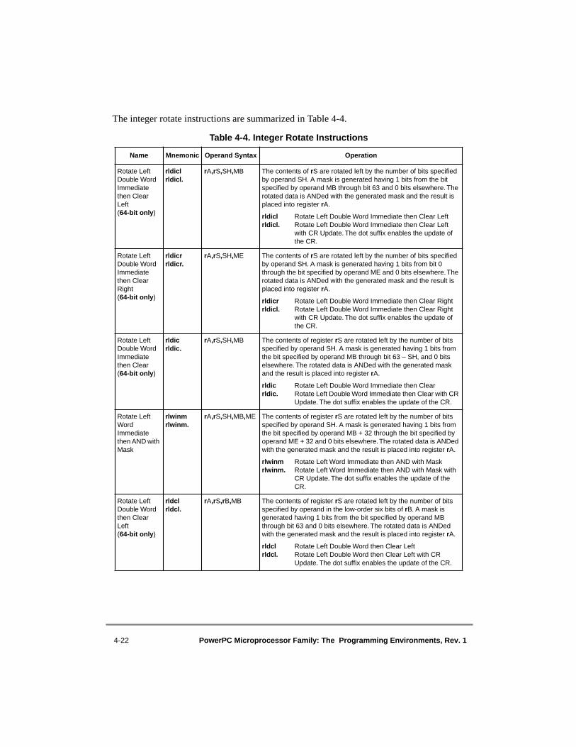
4-22 PowerPC Microprocessor Family: The Programming Environments, Rev. 1
The integer rotate instructions are summarized in Table 4-4.
Table 4-4. Integer Rotate Instructions
Name Mnemonic Operand Syntax Operation
Rotate Left Double Word Immediate then Clear Left (64-bit only)
rldiclrldicl.
rA,rS,SH,MB The contents of rS are rotated left by the number of bits specified by operand SH. A mask is generated having 1 bits from the bit specified by operand MB through bit 63 and 0 bits elsewhere. The rotated data is ANDed with the generated mask and the result is placed into register rA.
rldicl Rotate Left Double Word Immediate then Clear Leftrldicl. Rotate Left Double Word Immediate then Clear Left
with CR Update. The dot suffix enables the update of the CR.
Rotate Left Double Word Immediate then Clear Right(64-bit only)
rldicrrldicr.
rA,rS,SH,ME The contents of rS are rotated left by the number of bits specified by operand SH. A mask is generated having 1 bits from bit 0 through the bit specified by operand ME and 0 bits elsewhere. The rotated data is ANDed with the generated mask and the result is placed into register rA.
rldicr Rotate Left Double Word Immediate then Clear Rightrldicl. Rotate Left Double Word Immediate then Clear Right
with CR Update. The dot suffix enables the update of the CR.
Rotate Left Double Word Immediate then Clear(64-bit only)
rldicrldic.
rA,rS,SH,MB The contents of register rS are rotated left by the number of bits specified by operand SH. A mask is generated having 1 bits from the bit specified by operand MB through bit 63 – SH, and 0 bits elsewhere. The rotated data is ANDed with the generated mask and the result is placed into register rA.
rldic Rotate Left Double Word Immediate then Clear rldic. Rotate Left Double Word Immediate then Clear with CR
Update. The dot suffix enables the update of the CR.
Rotate Left Word Immediate then AND with Mask
rlwinmrlwinm.
rA,rS,SH,MB,ME The contents of register rS are rotated left by the number of bits specified by operand SH. A mask is generated having 1 bits from the bit specified by operand MB + 32 through the bit specified by operand ME + 32 and 0 bits elsewhere. The rotated data is ANDed with the generated mask and the result is placed into register rA.
rlwinm Rotate Left Word Immediate then AND with Maskrlwinm. Rotate Left Word Immediate then AND with Mask with
CR Update. The dot suffix enables the update of the CR.
Rotate Left Double Word then Clear Left(64-bit only)
rldclrldcl.
rA,rS,rB,MB The contents of register rS are rotated left by the number of bits specified by operand in the low-order six bits of rB. A mask is generated having 1 bits from the bit specified by operand MB through bit 63 and 0 bits elsewhere. The rotated data is ANDed with the generated mask and the result is placed into register rA.
rldcl Rotate Left Double Word then Clear Leftrldcl. Rotate Left Double Word then Clear Left with CR
Update. The dot suffix enables the update of the CR.

Chapter 4. Addressing Modes and Instruction Set Summary 4-23
4.2.1.4.2 Integer Shift InstructionsThe integer shift instructions perform left and right shifts. Immediate-form logical(unsigned) shift operations are obtained by specifying masks and shift values for certainrotate instructions. Simplified mnemonics (shown in Appendix F, “SimplifiedMnemonics”) are provided to make coding of such shifts simpler and easier to understand.
Any shift right algebraic instruction, followed by addze, can be used to divide quickly by2n. The setting of XER[CA] by the shift right algebraic instruction is independent of mode.
Multiple-precision shifts can be programmed as shown in Appendix C, “Multiple-PrecisionShifts.”
Rotate Left Double Word then Clear Right(64-bit only)
rldcrrldcr.
rA,rS,rB,ME The contents of register rS are rotated left by the number of bits specified by operand in the low-order six bits of rB. A mask is generated having 1 bits from bit 0 through the bit specified by operand ME and 0 bits elsewhere. The rotated data is ANDed with the generated mask and the result is placed into register rA.
rldcr Rotate Left Double Word then Clear Rightrldcr. Rotate Left Double Word then Clear Right with CR
Update. The dot suffix enables the update of the CR.
Rotate Left Word then AND with Mask
rlwnmrlwnm.
rA,rS,rB,MB,ME The contents of rS are rotated left by the number of bits specified by operand in the low-order five bits of rB. A mask is generated having 1 bits from the bit specified by operand MB + 32 through the bit specified by operand ME + 32 and 0 bits elsewhere. The rotated word is ANDed with the generated mask and the result is placed into rA.
rlwnm Rotate Left Word then AND with Maskrlwnm. Rotate Left Word then AND with Mask with CR Update.
The dot suffix enables the update of the CR.
Rotate Left Word Immediate then Mask Insert
rlwimirlwimi.
rA,rS,SH,MB,ME The contents of rS are rotated left by the number of bits specified by operand SH. A mask is generated having 1 bits from the bit specified by operand MB + 32 through the bit specified by operand ME + 32 and 0 bits elsewhere. The rotated word is inserted into rA under control of the generated mask.
rlwimi Rotate Left Word Immediate then Maskrlwimi. Rotate Left Word Immediate then Mask Insert with CR
Update. The dot suffix enables the update of the CR.
Rotate Left Double Word Immediate then Mask Insert(64-bit only)
rldimirldimi.
rA,rS,SH,MB The contents of rS are rotated left by the number of bits specified by operand SH. A mask is generated having 1 bits from the bit specified by operand MB through 63 – SH (the bit specified by SH), and 0 bits elsewhere. The rotated data is inserted into rA under control of the generated mask.
rldimi Rotate Left Word Immediate then Maskrldimi. Rotate Left Word Immediate then Mask Insert with CR
Update. The dot suffix enables the update of the CR.
Table 4-4. Integer Rotate Instructions (Continued)
Name Mnemonic Operand Syntax Operation

4-24 PowerPC Microprocessor Family: The Programming Environments, Rev. 1
The integer shift instructions are summarized in Table 4-5.
Table 4-5. Integer Shift Instructions
Name MnemonicOperand Syntax
Operation
Shift Left Double Word(64-bit only)
sldsld.
rA,rS,rB The contents of rS are shifted left the number of bits specified by the low-order seven bits of rB. Bits shifted out of position 0 are lost. Zeros are supplied to the vacated positions on the right. The result is placed into rA. Shift amounts from 64 to 127 give a zero result.
sld Shift Left Double Word sld. Shift Left Double Word with CR Update. The dot suffix enables
the update of the CR.
Shift Left Word
slwslw.
rA,rS,rB The contents of the low-order 32 bits of rS are shifted left the number of bits specified by operand in the low-order six bits of rB. Bits shifted out of position 32 (position 0 in 32-bit implementations) are lost. Zeros are supplied to the vacated positions on the right. The 32-bit result is placed into the low-order 32 bits of rA. In a 64-bit implementation, the value in the high-order 32 bits of rA is cleared, and shift amounts from 32 to 63 give a zero result.
slw Shift Left Word slw. Shift Left Word with CR Update. The dot suffix enables the update
of the CR.
Shift Right Double Word(64-bit only)
srdsrd.
rA,rS,rB The contents of rS are shifted right the number of bits specified by the low-order seven bits of rB. Bits shifted out of position 63 are lost. Zeros are supplied to the vacated positions on the left. The result is placed into rA. Shift amounts from 64 to 127 give a zero result.
srd Shift Right Double Word srd. Shift Right Double Word with CR Update. The dot suffix enables
the update of the CR.
Shift Right Word
srwsrw.
rA,rS,rB The contents of the low-order 32 bits of rS are shifted right the number of bits specified by the low-order six bits of rB. Bits shifted out of position 63 (position 31 in 32-bit implementations) are lost. Zeros are supplied to the vacated positions on the left. The 32-bit result is placed into the low-order 32 bits of rA. In a 64-bit implementation, the value in the high-order 32 bits of rA is cleared to zero, and shift amounts from 32 to 63 give a zero result.
srw Shift Right Word srw. Shift Right Word with CR Update. The dot suffix enables the
update of the CR.
Shift Right Algebraic Double Word Immediate(64-bit only)
sradisradi.
rA,rS,SH The contents of rS are shifted right the number of bits specified by operand SH. Bits shifted out of position 63 are lost. Bit 0 of rS is replicated to fill the vacated positions on the left. The result is placed into rA. XER[CA] is set if rS contains a negative number and any 1 bits are shifted out of position 63; otherwise XER[CA] is cleared. An operand SH of zero causes rA to be loaded with the contents of rS and XER[CA] to be cleared to zero.
sradi Shift Right Algebraic Double Word Immediatesradi. Shift Right Algebraic Double Word Immediate with CR Update.
The dot suffix enables the update of the CR.

Chapter 4. Addressing Modes and Instruction Set Summary 4-25
4.2.2 Floating-Point InstructionsThis section describes the floating-point instructions, which include the following:
• Floating-point arithmetic instructions• Floating-point multiply-add instructions• Floating-point rounding and conversion instructions• Floating-point compare instructions• Floating-point status and control register instructions• Floating-point move instructions
Note that MSR[FP] must be set in order for any of these instructions (including the floating-point loads and stores) to be executed. If MSR[FP] = 0 when any floating-point instructionis attempted, the floating-point unavailable exception is taken (see Section 6.4.8, “Floating-Point Unavailable Exception (0x00800)”). See Section 4.2.3, “Load and StoreInstructions,” for information about floating-point loads and stores.
The PowerPC architecture supports a floating-point system as defined in the IEEE-754standard, but requires software support to conform with that standard. Floating-pointoperations conform to the IEEE-754 standard, with the exception of operations performedwith the fmadd, fres, fsel, and frsqrte instructions, or if software sets the non-IEEE modebit (NI) in the FPSCR. Refer to Section 3.3, “Floating-Point Execution Models—UISA,”
Shift Right Algebraic Word Immediate
srawisrawi.
rA,rS,SH The contents of the low-order 32 bits of rS are shifted right the number of bits specified by operand SH. Bits shifted out of position 63 (position 31 in 32-bit implementations) are lost. Bit 32 of rS is replicated to fill the vacated positions on the left for 64-bit implementations. The 32-bit result is sign extended and placed into the low-order 32 bits of rA.
srawi Shift Right Algebraic Word Immediatesrawi. Shift Right Algebraic Word Immediate with CR Update. The dot
suffix enables the update of the CR.
Shift Right Algebraic Double Word(64-bit only)
sradsrad.
rA,rS,rB The contents of rS are shifted right the number of bits specified by the low-order seven bits of rB. Bits shifted out of position 63 are lost. Bit 0 of rS is replicated to fill the vacated positions on the left. The result is placed into rA.
srad Shift Right Algebraic Double Word srad. Shift Right Algebraic Double Word with CR Update. The dot suffix
enables the update of the CR.
Shift Right Algebraic Word
srawsraw.
rA,rS,rB The contents of the low-order 32 bits of rS are shifted right the number of bits specified by the low-order six bits of rB. Bits shifted out of position 63 (position 31 in 32-bit implementations) are lost. Bit 32 of rS is replicated to fill the vacated positions on the left for 64-bit implementations. The 32-bit result is placed into the low-order 32 bits of rA.
sraw Shift Right Algebraic Word sraw. Shift Right Algebraic Word with CR Update. The dot suffix
enables the update of the CR.
Table 4-5. Integer Shift Instructions (Continued)
Name MnemonicOperand Syntax
Operation

4-26 PowerPC Microprocessor Family: The Programming Environments, Rev. 1
for detailed information about the floating-point formats and exception conditions. Also,refer to Appendix D, “Floating-Point Models,” for more information on the floating-pointexecution models used by the PowerPC architecture.
4.2.2.1 Floating-Point Arithmetic InstructionsThe floating-point arithmetic instructions are summarized in Table 4-6.
Table 4-6. Floating-Point Arithmetic Instructions
Name MnemonicOperand Syntax
Operation
Floating Add(Double-Precision)
faddfadd.
frD,frA,frB The floating-point operand in register frA is added to the floating-point operand in register frB. If the most significant bit of the resultant significand is not a one the result is normalized. The result is rounded to the target precision under control of the floating-point rounding control field RN of the FPSCR and placed into register frD.
fadd Floating Add (Double-Precision)fadd. Floating Add (Double-Precision) with CR Update. The dot suffix
enables the update of the CR.
Floating Add Single
faddsfadds.
frD,frA,frB The floating-point operand in register frA is added to the floating-point operand in register frB. If the most significant bit of the resultant significand is not a one, the result is normalized. The result is rounded to the target precision under control of the floating-point rounding control field RN of the FPSCR and placed into register frD.
fadds Floating Add Single fadds. Floating Add Single with CR Update. The dot suffix enables the
update of the CR.
Floating Subtract (Double- Precision)
fsubfsub.
frD,frA,frB The floating-point operand in register frB is subtracted from the floating-point operand in register frA. If the most significant bit of the resultant significand is not 1, the result is normalized. The result is rounded to the target precision under control of the floating-point rounding control field RN of the FPSCR and placed into register frD.
fsub Floating Subtract (Double-Precision)fsub. Floating Subtract (Double-Precision) with CR Update. The dot
suffix enables the update of the CR.
Floating Subtract Single
fsubsfsubs.
frD,frA,frB The floating-point operand in register frB is subtracted from the floating-point operand in register frA. If the most significant bit of the resultant significand is not 1, the result is normalized. The result is rounded to the target precision under control of the floating-point rounding control field RN of the FPSCR and placed into frD.
fsubs Floating Subtract Single fsubs. Floating Subtract Single with CR Update. The dot suffix enables
the update of the CR.
Floating Multiply (Double-Precision)
fmulfmul.
frD,frA,frC The floating-point operand in register frA is multiplied by the floating-point operand in register frC.
fmul Floating Multiply (Double-Precision)fmul. Floating Multiply (Double-Precision) with CR Update. The dot
suffix enables the update of the CR.
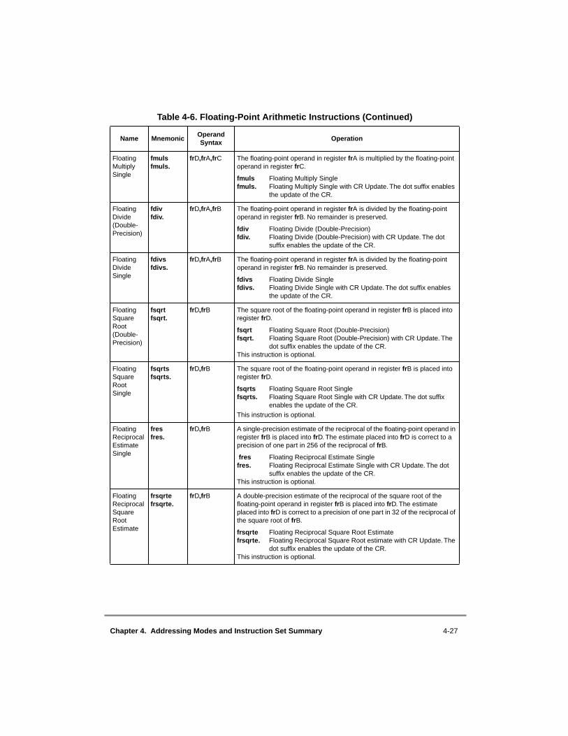
Chapter 4. Addressing Modes and Instruction Set Summary 4-27
Floating Multiply Single
fmulsfmuls.
frD,frA,frC The floating-point operand in register frA is multiplied by the floating-point operand in register frC.
fmuls Floating Multiply Single fmuls. Floating Multiply Single with CR Update. The dot suffix enables
the update of the CR.
Floating Divide(Double-Precision)
fdivfdiv.
frD,frA,frB The floating-point operand in register frA is divided by the floating-point operand in register frB. No remainder is preserved.
fdiv Floating Divide (Double-Precision)fdiv. Floating Divide (Double-Precision) with CR Update. The dot
suffix enables the update of the CR.
Floating Divide Single
fdivsfdivs.
frD,frA,frB The floating-point operand in register frA is divided by the floating-point operand in register frB. No remainder is preserved.
fdivs Floating Divide Singlefdivs. Floating Divide Single with CR Update. The dot suffix enables
the update of the CR.
Floating Square Root(Double-Precision)
fsqrtfsqrt.
frD,frB The square root of the floating-point operand in register frB is placed into register frD.
fsqrt Floating Square Root (Double-Precision)fsqrt. Floating Square Root (Double-Precision) with CR Update. The
dot suffix enables the update of the CR.This instruction is optional.
Floating Square Root Single
fsqrtsfsqrts.
frD,frB The square root of the floating-point operand in register frB is placed into register frD.
fsqrts Floating Square Root Singlefsqrts. Floating Square Root Single with CR Update. The dot suffix
enables the update of the CR.This instruction is optional.
Floating Reciprocal Estimate Single
fresfres.
frD,frB A single-precision estimate of the reciprocal of the floating-point operand in register frB is placed into frD. The estimate placed into frD is correct to a precision of one part in 256 of the reciprocal of frB.
fres Floating Reciprocal Estimate Singlefres. Floating Reciprocal Estimate Single with CR Update. The dot
suffix enables the update of the CR.This instruction is optional.
Floating Reciprocal Square Root Estimate
frsqrtefrsqrte.
frD,frB A double-precision estimate of the reciprocal of the square root of the floating-point operand in register frB is placed into frD. The estimate placed into frD is correct to a precision of one part in 32 of the reciprocal of the square root of frB.
frsqrte Floating Reciprocal Square Root Estimatefrsqrte. Floating Reciprocal Square Root estimate with CR Update. The
dot suffix enables the update of the CR.This instruction is optional.
Table 4-6. Floating-Point Arithmetic Instructions (Continued)
Name MnemonicOperand Syntax
Operation

4-28 PowerPC Microprocessor Family: The Programming Environments, Rev. 1
4.2.2.2 Floating-Point Multiply-Add InstructionsThese instructions combine multiply and add operations without an intermediate roundingoperation. The fractional part of the intermediate product is 106 bits wide, and all 106 bitstake part in the add/subtract portion of the instruction.
Status bits are set as follows:
• Overflow, underflow, and inexact exception bits, the FR and FI bits, and the FPRF field are set based on the final result of the operation, and not on the result of the multiplication.
• Invalid operation exception bits are set as if the multiplication and the addition were performed using two separate instructions (fmuls, followed by fadds or fsubs). That is, multiplication of infinity by zero or of anything by an SNaN, and/or addition of an SNaN, cause the corresponding exception bits to be set.
The floating-point multiply-add instructions are summarized in Table 4-7.
Floating Select
fsel frD,frA,frC,frB The floating-point operand in frA is compared to the value zero. If the operand is greater than or equal to zero, frD is set to the contents of frC. If the operand is less than zero or is a NaN, frD is set to the contents of frB. The comparison ignores the sign of zero (that is, regards +0 as equal to –0).
fsel Floating Selectfsel. Floating Select with CR Update. The dot suffix enables the
update of the CR.This instruction is optional.
Table 4-7. Floating-Point Multiply-Add Instructions
Name Mnemonic Operand Syntax Operation
Floating Multiply- Add (Double-Precision)
fmaddfmadd.
frD,frA,frC,frB The floating-point operand in register frA is multiplied by the floating-point operand in register frC. The floating-point operand in register frB is added to this intermediate result.
fmadd Floating Multiply-Add (Double-Precision)fmadd. Floating Multiply-Add (Double-Precision) with CR Update.
The dot suffix enables the update of the CR.
Floating Multiply- Add Single
fmaddsfmadds.
frD,frA,frC,frB The floating-point operand in register frA is multiplied by the floating-point operand in register frC. The floating-point operand in register frB is added to this intermediate result.
fmadds Floating Multiply-Add Single fmadds. Floating Multiply-Add Single with CR Update. The dot suffix
enables the update of the CR.
Table 4-6. Floating-Point Arithmetic Instructions (Continued)
Name MnemonicOperand Syntax
Operation

Chapter 4. Addressing Modes and Instruction Set Summary 4-29
For more information on multiply-add instructions, refer to Section D.2, “Execution Modelfor Multiply-Add Type Instructions.”
4.2.2.3 Floating-Point Rounding and Conversion InstructionsThe Floating Round to Single-Precision (frsp) instruction is used to truncate a 64-bitdouble-precision number to a 32-bit single-precision floating-point number. The floating-point convert instructions convert a 64-bit double-precision floating-point number to a 32-bit signed integer number.
Floating Multiply- Subtract (Double-Precision)
fmsubfmsub.
frD,frA,frC,frB The floating-point operand in register frA is multiplied by the floating-point operand in register frC. The floating-point operand in register frB is subtracted from this intermediate result.
fmsub Floating Multiply-Subtract (Double-Precision)fmsub. Floating Multiply-Subtract (Double-Precision) with CR
Update. The dot suffix enables the update of the CR.
Floating Multiply- Subtract Single
fmsubsfmsubs.
frD,frA,frC,frB The floating-point operand in register frA is multiplied by the floating-point operand in register frC. The floating-point operand in register frB is subtracted from this intermediate result.
fmsubs Floating Multiply-Subtract Singlefmsubs. Floating Multiply-Subtract Single with CR Update. The dot
suffix enables the update of the CR.
Floating Negative Multiply- Add (Double-Precision)
fnmaddfnmadd.
frD,frA,frC,frB The floating-point operand in register frA is multiplied by the floating-point operand in register frC. The floating-point operand in register frB is added to this intermediate result.
fnmadd Floating Negative Multiply-Add (Double-Precision)fnmadd. Floating Negative Multiply-Add (Double-Precision) with CR
Update. The dot suffix enables update of the CR.
Floating Negative Multiply- Add Single
fnmaddsfnmadds.
frD,frA,frC,frB The floating-point operand in register frA is multiplied by the floating-point operand in register frC. The floating-point operand in register frB is added to this intermediate result.
fnmadds Floating Negative Multiply-Add Single fnmadds. Floating Negative Multiply-Add Single with CR Update. The
dot suffix enables the update of the CR.
Floating Negative Multiply- Subtract (Double-Precision)
fnmsubfnmsub.
frD,frA,frC,frB The floating-point operand in register frA is multiplied by the floating-point operand in register frC. The floating-point operand in register frB is subtracted from this intermediate result.
fnmsub Floating Negative Multiply-Subtract (Double-Precision)fnmsub. Floating Negative Multiply-Subtract (Double-Precision) with
CR Update. The dot suffix enables the update of the CR.
Floating Negative Multiply- Subtract Single
fnmsubsfnmsubs.
frD,frA,frC,frB The floating-point operand in register frA is multiplied by the floating-point operand in register frC. The floating-point operand in register frB is subtracted from this intermediate result.
fnmsubs Floating Negative Multiply-Subtract Singlefnmsubs. Floating Negative Multiply-Subtract Single with CR Update.
The dot suffix enables the update of the CR.
Table 4-7. Floating-Point Multiply-Add Instructions (Continued)
Name Mnemonic Operand Syntax Operation

4-30 PowerPC Microprocessor Family: The Programming Environments, Rev. 1
The PowerPC architecture defines bits 0–31 of floating-point register frD as undefinedwhen executing the Floating Convert to Integer Word (fctiw) and Floating Convert toInteger Word with Round toward Zero (fctiwz) instructions. The floating-point roundinginstructions are shown in Table 4-8.
Examples of uses of these instructions to perform various conversions can be found inAppendix D, “Floating-Point Models.”
Table 4-8. Floating-Point Rounding and Conversion Instructions
Name MnemonicOperand Syntax
Operation
Floating Round to Single- Precision
frspfrsp.
frD,frB The floating-point operand in frB is rounded to single-precision using the rounding mode specified by FPSCR[RN] and placed into frD.
frsp Floating Round to Single-Precision frsp. Floating Round to Single-Precision with CR Update. The dot
suffix enables the update of the CR.
Floating Convert from Integer Double Word(64-bit only)
fcfidfcfid.
frD,frB The 64-bit signed integer operand in frB is converted to an infinitely precise floating-point integer. The result of the conversion is rounded to double-precision using the rounding mode specified by FPSCR[RN] and placed into register frD.
fcfid Floating Convert from Integer Double Wordfcfid. Floating Convert from Integer Double Word with CR Update. The
dot suffix enables the update of the CR.
Floating Convert to Integer Double Word(64-bit only)
fctidfctid.
frD,frB The floating-point operand in register frB is converted to a 64-bit signed integer, using the rounding mode specified by FPSCR[RN], and placed in frD.
fctiw Floating Convert to Integer Double Word fctiw. Floating Convert to Integer Double Word with CR Update. The
dot suffix enables the update of the CR.
Floating Convert to Integer Double Word with Round toward Zero(64-bit only)
fctidzfctidz.
frD,frB The floating-point operand in register frB is converted to a 64-bit signed integer, using the rounding mode Round toward Zero and placed in frD.
fctidz Floating Convert to Integer Double Word with Round toward Zerofctidz. Floating Convert to Integer Double Word with Round toward Zero
with CR Update. The dot suffix enables the update of the CR.
Floating Convert to Integer Word
fctiwfctiw.
frD,frB The floating-point operand in register frB is converted to a 32-bit signed integer, using the rounding mode specified by FPSCR[RN], and placed in the low-order 32 bits of frD. Bits 0–31 of frD are undefined.
fctiw Floating Convert to Integer Word fctiw. Floating Convert to Integer Word with CR Update. The dot suffix
enables the update of the CR.
Floating Convert to Integer Word with Round toward Zero
fctiwzfctiwz.
frD,frB The floating-point operand in register frB is converted to a 32-bit signed integer, using the rounding mode Round toward Zero, and placed in the low-order 32 bits of frD. Bits 0–31 of frD are undefined.
fctiwz Floating Convert to Integer Word with Round toward Zero fctiwz. Floating Convert to Integer Word with Round toward Zero with
CR Update. The dot suffix enables the update of the CR.
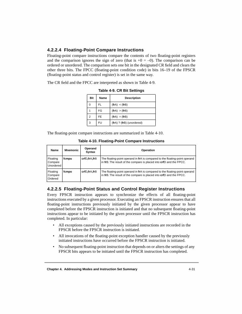
Chapter 4. Addressing Modes and Instruction Set Summary 4-31
4.2.2.4 Floating-Point Compare InstructionsFloating-point compare instructions compare the contents of two floating-point registersand the comparison ignores the sign of zero (that is +0 = –0). The comparison can beordered or unordered. The comparison sets one bit in the designated CR field and clears theother three bits. The FPCC (floating-point condition code) in bits 16–19 of the FPSCR(floating-point status and control register) is set in the same way.
The CR field and the FPCC are interpreted as shown in Table 4-9.
The floating-point compare instructions are summarized in Table 4-10.
4.2.2.5 Floating-Point Status and Control Register InstructionsEvery FPSCR instruction appears to synchronize the effects of all floating-pointinstructions executed by a given processor. Executing an FPSCR instruction ensures that allfloating-point instructions previously initiated by the given processor appear to havecompleted before the FPSCR instruction is initiated and that no subsequent floating-pointinstructions appear to be initiated by the given processor until the FPSCR instruction hascompleted. In particular:
• All exceptions caused by the previously initiated instructions are recorded in the FPSCR before the FPSCR instruction is initiated.
• All invocations of the floating-point exception handler caused by the previously initiated instructions have occurred before the FPSCR instruction is initiated.
• No subsequent floating-point instruction that depends on or alters the settings of any FPSCR bits appears to be initiated until the FPSCR instruction has completed.
Table 4-9. CR Bit Settings
Bit Name Description
0 FL (frA) < (frB)
1 FG (frA) > (frB)
2 FE (frA) = (frB)
3 FU (frA) ? (frB) (unordered)
Table 4-10. Floating-Point Compare Instructions
Name MnemonicOperand Syntax
Operation
Floating Compare Unordered
fcmpu crfD,frA,frB The floating-point operand in frA is compared to the floating-point operand in frB. The result of the compare is placed into crfD and the FPCC.
Floating Compare Ordered
fcmpo crfD,frA,frB The floating-point operand in frA is compared to the floating-point operand in frB. The result of the compare is placed into crfD and the FPCC.

4-32 PowerPC Microprocessor Family: The Programming Environments, Rev. 1
Floating-point memory access instructions are not affected by the execution of the FPSCRinstructions.
The FPSCR instructions are summarized in Table 4-11.
Table 4-11. Floating-Point Status and Control Register Instructions
Name MnemonicOperand Syntax
Operation
Move from FPSCR
mffsmffs.
frD The contents of the FPSCR are placed into bits 32–63 of frD. Bits 0–31 of frD are undefined.
mffs Move from FPSCRmffs. Move from FPSCR with CR Update. The dot suffix enables the
update of the CR.
Move to Condition Register from FPSCR
mcrfs crfD,crfS The contents of FPSCR field specified by operand crfS are copied to the CR field specified by operand crfD. All exception bits copied (except FEX and VX bits) are cleared in the FPSCR.
Move to FPSCR Field Immediate
mtfsfimtfsfi.
crfD,IMM The contents of the IMM field are placed into FPSCR field crfD. The contents of FPSCR[FX] are altered only if crfD = 0.
mtfsfi Move to FPSCR Field Immediatemtfsfi. Move to FPSCR Field Immediate with CR Update. The dot
suffix enables the update of the CR.
Move to FPSCR Fields
mtfsfmtfsf.
FM,frB Bits 32–63 of frB are placed into the FPSCR under control of the field mask specified by FM. The field mask identifies the 4-bit fields affected. Let i be an integer in the range 0–7. If FM[i] = 1, FPSCR field i (FPSCR bits 4∗ i through 4∗ i+3) is set to the contents of the corresponding field of the low-order 32 bits of frB.
The contents of FPSCR[FX] are altered only if FM[0] = 1.
mtfsf Move to FPSCR Fields mtfsf. Move to FPSCR Fields with CR Update. The dot suffix enables
the update of the CR.
Move to FPSCR Bit 0
mtfsb0mtfsb0.
crbD The FPSCR bit location specified by operand crbD is cleared.
Bits 1 and 2 (FEX and VX) cannot be reset explicitly.
mtfsb0 Move to FPSCR Bit 0mtfsb0. Move to FPSCR Bit 0 with CR Update. The dot suffix enables
the update of the CR.
Move to FPSCR Bit 1
mtfsb1mtfsb1.
crbD The FPSCR bit location specified by operand crbD is set.
Bits 1 and 2 (FEX and VX) cannot be set explicitly.
mtfsb1 Move to FPSCR Bit 1mtfsb1. Move to FPSCR Bit 1 with CR Update. The dot suffix enables
the update of the CR.

Chapter 4. Addressing Modes and Instruction Set Summary 4-33
4.2.2.6 Floating-Point Move InstructionsFloating-point move instructions copy data from one FPR to another, altering the sign bit(bit 0) as described for the fneg, fabs, and fnabs instructions in Table 4-12. The fneg, fabs,and fnabs instructions may alter the sign bit of a NaN. The floating-point move instructionsdo not modify the FPSCR. The CR update option in these instructions controls the placingof result status into CR1. If the CR update option is enabled, CR1 is set; otherwise, CR1 isunchanged.
Table 4-12 provides a summary of the floating-point move instructions.
4.2.3 Load and Store InstructionsLoad and store instructions are issued and translated in program order; however, theaccesses can occur out of order. Synchronizing instructions are provided to enforce strictordering. This section describes the load and store instructions, which consist of thefollowing:
• Integer load instructions• Integer store instructions• Integer load and store with byte-reverse instructions• Integer load and store multiple instructions• Floating-point load instructions• Floating-point store instructions• Memory synchronization instructions
Table 4-12. Floating-Point Move Instructions
Name Mnemonic Operand Syntax Operation
Floating Move Register
fmrfmr.
frD,frB The contents of frB are placed into frD.
fmr Floating Move Registerfmr. Floating Move Register with CR Update. The dot suffix
enables the update of the CR.
Floating Negate
fnegfneg.
frD,frB The contents of frB with bit 0 inverted are placed into frD.
fneg Floating Negatefneg. Floating Negate with CR Update. The dot suffix enables the
update of the CR.
Floating Absolute Value
fabsfabs.
frD,frB The contents of frB with bit 0 cleared are placed into frD.
fabs Floating Absolute Value fabs. Floating Absolute Value with CR Update. The dot suffix
enables the update of the CR.
Floating Negative Absolute Value
fnabsfnabs.
frD,frB The contents of frB with bit 0 set are placed into frD.
fnabs Floating Negative Absolute Valuefnabs. Floating Negative Absolute Value with CR Update. The dot
suffix enables the update of the CR.

4-34 PowerPC Microprocessor Family: The Programming Environments, Rev. 1
4.2.3.1 Integer Load and Store Address GenerationInteger load and store operations generate effective addresses using register indirect withimmediate index mode, register indirect with index mode, or register indirect mode. SeeSection 4.1.4.2, “Effective Address Calculation,” for information about calculatingeffective addresses. Note that in some implementations, operations that are not naturallyaligned may suffer performance degradation. Refer to Section 6.4.6.1, “Integer AlignmentExceptions,” for additional information about load and store address alignment exceptions.
4.2.3.1.1 Register Indirect with Immediate Index Addressing for Integer Loads and Stores
Instructions using this addressing mode contain a signed 16-bit immediate index(d operand) which is sign extended, and added to the contents of a general-purpose registerspecified in the instruction (rA operand) to generate the effective address. If the rA field ofthe instruction specifies r0, a value of zero is added to the immediate index (d operand) inplace of the contents of r0. The option to specify rA or 0 is shown in the instructiondescriptions as (rA|0).
Figure 4-1 shows how an effective address is generated when using register indirect withimmediate index addressing.
.
Figure 4-1. Register Indirect with Immediate Index Addressing for Integer Loads/Stores
No
0 47 48 63
Sign Extension d
0 63
GPR (rA)
0
0 63
GPR (rD/rS)StoreLoad
Yes
Instruction Encoding:0 5 6 1011 15 16 31
Opcode rD/rS rA d
+0 63
Effective Address
rA=0?
Memory Interface

Chapter 4. Addressing Modes and Instruction Set Summary 4-35
4.2.3.1.2 Register Indirect with Index Addressing for Integer Loads and Stores
Instructions using this addressing mode cause the contents of two general-purpose registers(specified as operands rA and rB) to be added in the generation of the effective address. Azero in place of the rA operand causes a zero to be added to the contents of the general-purpose register specified in operand rB (or the value zero for lswi and stswi instructions).The option to specify rA or 0 is shown in the instruction descriptions as (rA|0).
Figure 4-2 shows how an effective address is generated when using register indirect withindex addressing.
Figure 4-2. Register Indirect with Index Addressing for Integer Loads/Stores
4.2.3.1.3 Register Indirect Addressing for Integer Loads and Stores Instructions using this addressing mode use the contents of the general-purpose registerspecified by the rA operand as the effective address. A zero in the rA operand causes aneffective address of zero to be generated. The option to specify rA or 0 is shown in theinstruction descriptions as (rA|0).
Figure 4-3 shows how an effective address is generated when using register indirectaddressing.
No
0 63
GPR (rA)
0
+
0 63
GPR (rD/rS)Memory Interface
StoreLoad
Yes
0 63
GPR (rB)
Instruction Encoding:
rA=0?
0 63
Effective Address
0 5 6 1011 15 16 20 21 30 31
Opcode rD/rS rA rB Subopcode 0Reserved

4-36 PowerPC Microprocessor Family: The Programming Environments, Rev. 1
Figure 4-3. Register Indirect Addressing for Integer Loads/Stores
4.2.3.2 Integer Load InstructionsFor integer load instructions, the byte, half word, word, or double word addressed by theEA (effective address) is loaded into rD. Many integer load instructions have an updateform, in which rA is updated with the generated effective address. For these forms, if rA ≠0 and rA ≠ rD (otherwise invalid), the EA is placed into rA and the memory element (byte,half word, word, or double word) addressed by the EA is loaded into rD. Note that thePowerPC architecture defines load with update instructions with operand rA = 0 orrA = rD as invalid forms.
The default byte and bit ordering is big-endian in the PowerPC architecture; seeSection 3.1.2, “Byte Ordering,” for information about little-endian byte ordering.
Note that in some implementations of the architecture, the load word algebraic instructions(lha, lhax, lwa, lwax) and the load with update (lbzu, lbzux, lhzu, lhzux, lhau, lhaux,lwaux, ldu, ldux) instructions may execute with greater latency than other types of loadinstructions. Moreover, the load with update instructions may take longer to execute insome implementations than the corresponding pair of a nonupdate load followed by an addinstruction.
No
StoreLoad
Yes0 63
0 0 0 0 0 0 0 0 0 0 0 0 0 0 0 0 0 0 0 0 0 0 0 0 0 0 0 0 0 0 0 0
Instruction Encoding:0 5 6 10 11 15 16 20 21 30 31
rA=0?
0 63
GPR (rA)
0 63
Effective Address
Opcode rD/rS rA NB Subopcode 0
0 63
GPR (rD/rS)Memory Interface
Reserved
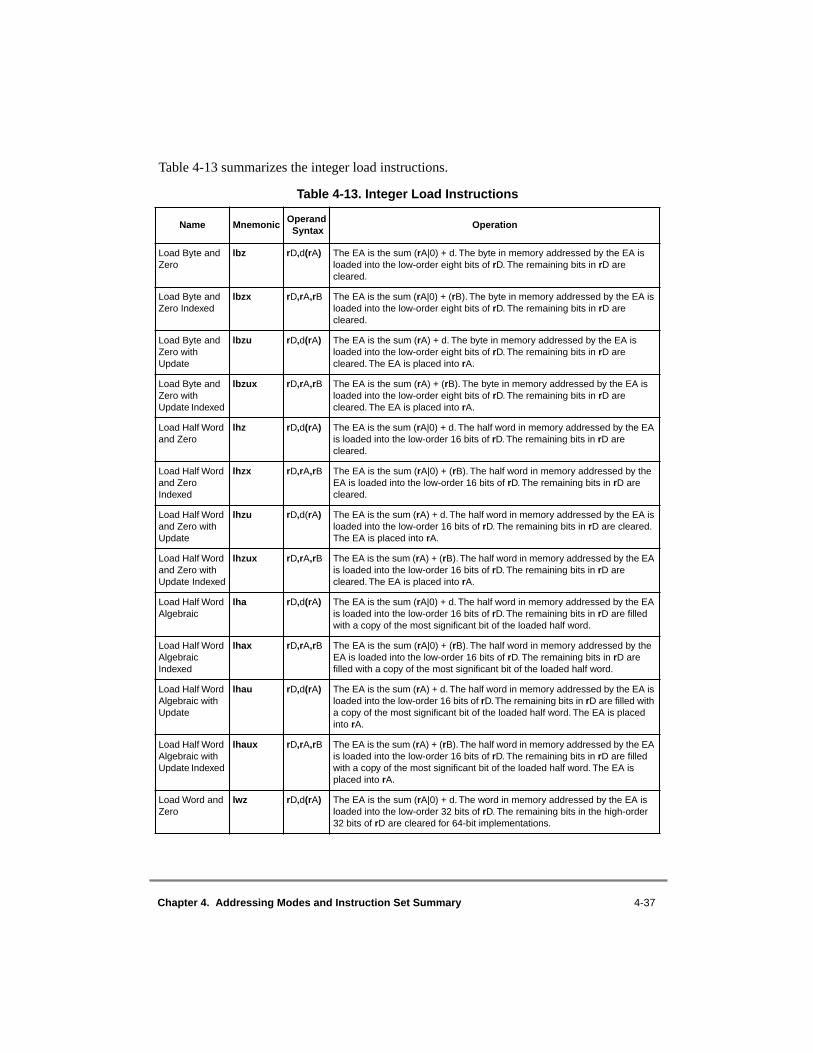
Chapter 4. Addressing Modes and Instruction Set Summary 4-37
Table 4-13 summarizes the integer load instructions.
Table 4-13. Integer Load Instructions
Name MnemonicOperand Syntax
Operation
Load Byte and Zero
lbz rD,d(rA) The EA is the sum (rA|0) + d. The byte in memory addressed by the EA is loaded into the low-order eight bits of rD. The remaining bits in rD are cleared.
Load Byte and Zero Indexed
lbzx rD,rA,rB The EA is the sum (rA|0) + (rB). The byte in memory addressed by the EA is loaded into the low-order eight bits of rD. The remaining bits in rD are cleared.
Load Byte and Zero with Update
lbzu rD,d(rA) The EA is the sum (rA) + d. The byte in memory addressed by the EA is loaded into the low-order eight bits of rD. The remaining bits in rD are cleared. The EA is placed into rA.
Load Byte and Zero with Update Indexed
lbzux rD,rA,rB The EA is the sum (rA) + (rB). The byte in memory addressed by the EA is loaded into the low-order eight bits of rD. The remaining bits in rD are cleared. The EA is placed into rA.
Load Half Word and Zero
lhz rD,d(rA) The EA is the sum (rA|0) + d. The half word in memory addressed by the EA is loaded into the low-order 16 bits of rD. The remaining bits in rD are cleared.
Load Half Word and Zero Indexed
lhzx rD,rA,rB The EA is the sum (rA|0) + (rB). The half word in memory addressed by the EA is loaded into the low-order 16 bits of rD. The remaining bits in rD are cleared.
Load Half Word and Zero with Update
lhzu rD,d(rA) The EA is the sum (rA) + d. The half word in memory addressed by the EA is loaded into the low-order 16 bits of rD. The remaining bits in rD are cleared. The EA is placed into rA.
Load Half Word and Zero with Update Indexed
lhzux rD,rA,rB The EA is the sum (rA) + (rB). The half word in memory addressed by the EA is loaded into the low-order 16 bits of rD. The remaining bits in rD are cleared. The EA is placed into rA.
Load Half Word Algebraic
lha rD,d(rA) The EA is the sum (rA|0) + d. The half word in memory addressed by the EA is loaded into the low-order 16 bits of rD. The remaining bits in rD are filled with a copy of the most significant bit of the loaded half word.
Load Half Word Algebraic Indexed
lhax rD,rA,rB The EA is the sum (rA|0) + (rB). The half word in memory addressed by the EA is loaded into the low-order 16 bits of rD. The remaining bits in rD are filled with a copy of the most significant bit of the loaded half word.
Load Half Word Algebraic with Update
lhau rD,d(rA) The EA is the sum (rA) + d. The half word in memory addressed by the EA is loaded into the low-order 16 bits of rD. The remaining bits in rD are filled with a copy of the most significant bit of the loaded half word. The EA is placed into rA.
Load Half Word Algebraic with Update Indexed
lhaux rD,rA,rB The EA is the sum (rA) + (rB). The half word in memory addressed by the EA is loaded into the low-order 16 bits of rD. The remaining bits in rD are filled with a copy of the most significant bit of the loaded half word. The EA is placed into rA.
Load Word and Zero
lwz rD,d(rA) The EA is the sum (rA|0) + d. The word in memory addressed by the EA is loaded into the low-order 32 bits of rD. The remaining bits in the high-order 32 bits of rD are cleared for 64-bit implementations.

4-38 PowerPC Microprocessor Family: The Programming Environments, Rev. 1
4.2.3.3 Integer Store Instructions For integer store instructions, the contents of rS are stored into the byte, half word, word ordouble word in memory addressed by the EA (effective address). Many store instructionshave an update form, in which rA is updated with the EA. For these forms, the followingrules apply:
• If rA ≠ 0, the effective address is placed into rA.
• If rS = rA, the contents of register rS are copied to the target memory element, then the generated EA is placed into rA (rS).
Load Word and Zero Indexed
lwzx rD,rA,rB The EA is the sum (rA|0) + (rB). The word in memory addressed by the EA is loaded into the low-order 32 bits of rD. The remaining bits in the high-order 32 bits of rD are cleared for 64-bit implementations.
Load Word and Zero with Update
lwzu rD,d(rA) The EA is the sum (rA) + d. The word in memory addressed by the EA is loaded into the low-order 32 bits of rD. The remaining bits in the high-order 32 bits of rD are cleared for 64-bit implementations. The EA is placed into rA.
Load Word and Zero with Update Indexed
lwzux rD,rA,rB The EA is the sum (rA) + (rB). The word in memory addressed by the EA is loaded into the low-order 32 bits of rD. The remaining bits in the high-order 32 bits of rD are cleared for 64-bit implementations. The EA is placed into rA.
Load Word Algebraic(64-bit only)
lwa rD,ds(rA) The EA is the sum (rA|0) + (ds||0b00). The word in memory addressed by the EA is loaded into the low-order 32 bits of rD. The remaining bits in the high-order 32 bits of rD are filled with a copy of the most significant bit of the loaded word.
Load Word Algebraic Indexed(64-bit only)
lwax rD,rA,rB The EA is the sum (rA|0) + (rB). The word in memory addressed by the EA is loaded into the low-order 32 bits of rD. The remaining bits in the high-order 32 bits of rD are filled with a copy of the most significant bit of the loaded word.
Load Word Algebraic with Update Indexed(64-bit only)
lwaux rD,rA,rB The EA is the sum (rA) + (rB). The word in memory addressed by the EA is loaded into the low-order 32 bits of rD. The remaining bits in the high-order 32 bits of rD are filled with a copy of the most significant bit of the loaded word. The EA is placed into rA.
Load Double Word(64-bit only)
ld rD,ds(rA) The EA is the sum (rA|0) + (ds||0b00). The double word in memory addressed by the EA is loaded into rD.
Load Double Word Indexed(64-bit only)
ldx rD,rA,rB The EA is the sum (rA|0) + (rB). The double word in memory addressed by the EA is loaded into rD.
Load Double Word with Update(64-bit only)
ldu rD,ds(rA) The EA is the sum (rA) + (ds||0b00). The double word in memory addressed by the EA is loaded into rD. The EA is placed into rA.
Load Double Word with Update Indexed(64-bit only)
ldux rD,rA,rB The EA is the sum (rA) + (rB). The double word in memory addressed by the EA is loaded into rD. The EA is placed into rA.
Table 4-13. Integer Load Instructions (Continued)
Name MnemonicOperand Syntax
Operation

Chapter 4. Addressing Modes and Instruction Set Summary 4-39
In general, the PowerPC architecture defines a sequential execution model. However, whena store instruction modifies a memory location that contains an instruction, softwaresynchronization is required to ensure that subsequent instruction fetches from that locationobtain the modified version of the instruction.
If a program modifies the instructions it intends to execute, it should call the appropriatesystem library program before attempting to execute the modified instructions to ensurethat the modifications have taken effect with respect to instruction fetching.
The PowerPC architecture defines store with update instructions with rA = 0 as an invalidform. In addition, it defines integer store instructions with the CR update option enabled(Rc field, bit 31, in the instruction encoding = 1) to be an invalid form. Table 4-14 providesa summary of the integer store instructions.
Table 4-14. Integer Store Instructions
Name MnemonicOperand Syntax
Operation
Store Byte stb rS,d(rA) The EA is the sum (rA|0) + d. The contents of the low-order eight bits of rS are stored into the byte in memory addressed by the EA.
Store Byte Indexed stbx rS,rA,rB The EA is the sum (rA|0) + (rB). The contents of the low-order eight bits of rS are stored into the byte in memory addressed by the EA.
Store Byte with Update
stbu rS,d(rA) The EA is the sum (rA) + d. The contents of the low-order eight bits of rS are stored into the byte in memory addressed by the EA. The EA is placed into rA.
Store Byte with Update Indexed
stbux rS,rA,rB The EA is the sum (rA) + (rB). The contents of the low-order eight bits of rS are stored into the byte in memory addressed by the EA. The EA is placed into rA.
Store Half Word sth rS,d(rA) The EA is the sum (rA|0) + d. The contents of the low-order 16 bits of rS are stored into the half word in memory addressed by the EA.
Store Half Word Indexed
sthx rS,rA,rB The EA is the sum (rA|0) + (rB). The contents of the low-order 16 bits of rS are stored into the half word in memory addressed by the EA.
Store Half Word with Update
sthu rS,d(rA) The EA is the sum (rA) + d. The contents of the low-order 16 bits of rS are stored into the half word in memory addressed by the EA. The EA is placed into rA.
Store Half Word with Update Indexed
sthux rS,rA,rB The EA is the sum (rA) + (rB). The contents of the low-order 16 bits of rS are stored into the half word in memory addressed by the EA. The EA is placed into rA.
Store Word stw rS,d(rA) The EA is the sum (rA|0) + d. The contents of the low-order 32 bits of rS are stored into the word in memory addressed by the EA.
Store Word Indexed stwx rS,rA,rB The EA is the sum (rA|0) + (rB). The contents of the low-order 32 bits of rS are stored into the word in memory addressed by the EA.
Store Word with Update
stwu rS,d(rA) The EA is the sum (rA) + d. The contents of the low-order 32 bits of rS are stored into the word in memory addressed by the EA. The EA is placed into rA.

4-40 PowerPC Microprocessor Family: The Programming Environments, Rev. 1
4.2.3.4 Integer Load and Store with Byte-Reverse InstructionsTable 4-15 describes integer load and store with byte-reverse instructions. Note that insome PowerPC implementations, load byte-reverse instructions may have greater latencythan other load instructions.
When used in a PowerPC system operating with the default big-endian byte order, theseinstructions have the effect of loading and storing data in little-endian order. Likewise,when used in a PowerPC system operating with little-endian byte order, these instructionshave the effect of loading and storing data in big-endian order. For more information aboutbig-endian and little-endian byte ordering, see Section 3.1.2, “Byte Ordering.”
Store Word with Update Indexed
stwux rS,rA,rB The EA is the sum (rA) + (rB). The contents of the low-order 32 bits of rS are stored into the word in memory addressed by the EA. The EA is placed into rA.
Store Double Word(64-bit only)
std rS,ds(rA) The EA is the sum (rA|0) + (ds||0b00). The contents of rS are stored into the double word in memory addressed by the EA.
Store Double Word Indexed(64-bit only)
stdx rS,rA,rB The EA is the sum (rA|0) + (rB). The contents of rS are stored into the double word in memory addressed by the EA.
Store Double Word with Update(64-bit only)
stdu rS,ds(rA) The EA is the sum (rA) + (ds||0b00). The contents of rS are stored into the double word in memory addressed by the EA. The EA is placed into rA.
Store Double Word with Update Indexed(64-bit only)
stdux rS,rA,rB The EA is the sum (rA) + (rB). The contents of rS are stored into the double word in memory addressed by the EA. The EA is placed into rA.
Table 4-15. Integer Load and Store with Byte-Reverse Instructions
Name MnemonicOperand Syntax
Operation
Load Half Word Byte-Reverse Indexed
lhbrx rD,rA,rB The EA is the sum (rA|0) + (rB). The high-order eight bits of the half word addressed by the EA are loaded into the low-order eight bits of rD. The next eight higher-order bits of the half word in memory addressed by the EA are loaded into the next eight lower-order bits of rD. The remaining rD bits are cleared.
Load Word Byte- Reverse Indexed
lwbrx rD,rA,rB The EA is the sum (rA|0) + (rB). Bits 0–7 of the word in memory addressed by the EA are loaded into the low-order eight bits of rD. Bits 8–15 of the word in memory addressed by the EA are loaded into bits 48–55 of rD (bits 16–23 of rD in 32-bit implementations). Bits 16–23 of the word in memory addressed by the EA are loaded into bits 40–47 of rD (bits 8–15 in 32-bit implementations). Bits 24–31 of the word in memory addressed by the EA are loaded into bits 32–39 of rD (bits 0–7 in 32-bit implementations). The remaining bits in rD are cleared.
Table 4-14. Integer Store Instructions (Continued)
Name MnemonicOperand Syntax
Operation

Chapter 4. Addressing Modes and Instruction Set Summary 4-41
4.2.3.5 Integer Load and Store Multiple InstructionsThe load/store multiple instructions are used to move blocks of data to and from the GPRs.The load multiple and store multiple instructions may have operands that require memoryaccesses crossing a 4-Kbyte page boundary. As a result, these instructions may beinterrupted by a DSI exception associated with the address translation of the second page.Table 4-16 summarizes the integer load and store multiple instructions.
In the load/store multiple instructions, the combination of the EA and rD (rS) is such thatthe low-order byte of GPR31 is loaded from or stored into the last byte of an aligned quadword in memory; if the effective address is not correctly aligned, it may take significantlylonger to execute.
In some PowerPC implementations operating with little-endian byte order, execution of anlmw or stmw instruction causes the system alignment error handler to be invoked; seeSection 3.1.2, “Byte Ordering,” for more information.
The PowerPC architecture defines the load multiple word (lmw) instruction with rA in therange of registers to be loaded, including the case in which rA = 0, as an invalid form.
Store Half Word Byte- Reverse Indexed
sthbrx rS,rA,rB The EA is the sum (rA|0) + (rB). The contents of the low-order eight bits of rS are stored into the high-order eight bits of the half word in memory addressed by the EA. The contents of the next lower-order eight bits of rS are stored into the next eight higher-order bits of the half word in memory addressed by the EA.
Store Word Byte- Reverse Indexed
stwbrx rS,rA,rB The effective address is the sum (rA|0) + (rB). The contents of the low-order eight bits of rS are stored into bits 0–7 of the word in memory addressed by EA. The contents of the next eight lower-order bits of rS are stored into bits 8–15 of the word in memory addressed by the EA. The contents of the next eight lower-order bits of rS are stored into bits 16–23 of the word in memory addressed by the EA. The contents of the next eight lower-order bits of rS are stored into bits 24–31 of the word addressed by the EA.
Table 4-16. Integer Load and Store Multiple Instructions
Name MnemonicOperand Syntax
Operation
Load Multiple Word lmw rD,d(rA) The EA is the sum (rA|0) + d. n = (32 – rD).
Store Multiple Word stmw rS,d(rA) The EA is the sum (rA|0) + d. n = (32 – rS).
Table 4-15. Integer Load and Store with Byte-Reverse Instructions (Continued)
Name MnemonicOperand Syntax
Operation

4-42 PowerPC Microprocessor Family: The Programming Environments, Rev. 1
4.2.3.6 Integer Load and Store String InstructionsThe integer load and store string instructions allow movement of data from memory toregisters or from registers to memory without concern for alignment. These instructions canbe used for a short move between arbitrary memory locations or to initiate a long movebetween misaligned memory fields. However, in some implementations, these instructionsare likely to have greater latency and take longer to execute, perhaps much longer, than asequence of individual load or store instructions that produce the same results. Table 4-17summarizes the integer load and store string instructions.
Load and store string instructions execute more efficiently when rD or rS = 5, and the lastregister loaded or stored is less than or equal to 12.
In some PowerPC implementations operating with little-endian byte order, execution of aload or string instruction causes the system alignment error handler to be invoked; seeSection 3.1.2, “Byte Ordering,” for more information.
Load string and store string instructions may involve operands that are not word-aligned.As described in Section 6.4.6, “Alignment Exception (0x00600),” a misaligned stringoperation suffers a performance penalty compared to an aligned operation of the same type.A non–word-aligned string operation that crosses a double-word boundary is also slowerthan a word-aligned string operation.
4.2.3.7 Floating-Point Load and Store Address GenerationFloating-point load and store operations generate effective addresses using the registerindirect with immediate index addressing mode and register indirect with index addressingmode. Floating-point loads and stores are not supported for direct-store interface accesses.The use of floating-point loads and stores for direct-store interface accesses results in analignment exception. Note that the direct-store facility is being phased out of thearchitecture and is not likely to be supported in future devices.
Table 4-17. Integer Load and Store String Instructions
Name Mnemonic Operand Syntax Operation
Load String Word Immediate lswi rD,rA,NB The EA is (rA|0).
Load String Word Indexed lswx rD,rA,rB The EA is the sum (rA|0) + (rB).
Store String Word Immediate stswi rS,rA,NB The EA is (rA|0).
Store String Word Indexed stswx rS,rA,rB The EA is the sum (rA|0) + (rB).

Chapter 4. Addressing Modes and Instruction Set Summary 4-43
4.2.3.7.1 Register Indirect with Immediate Index Addressing for Floating-Point Loads and Stores
Instructions using this addressing mode contain a signed 16-bit immediate index(d operand) which is sign extended to 64 bits, and added to the contents of a GPR specifiedin the instruction (rA operand) to generate the effective address. If the rA field of theinstruction specifies r0, a value of zero is added to the immediate index (d operand) in placeof the contents of r0. The option to specify rA or 0 is shown in the instruction descriptionsas (rA|0).
Figure 4-4 shows how an effective address is generated when using register indirect withimmediate index addressing for floating-point loads and stores.
Figure 4-4. Register Indirect with Immediate Index Addressing for Floating-Point Loads/Stores
4.2.3.7.2 Register Indirect with Index Addressing for Floating-Point Loads and Stores
Instructions using this addressing mode add the contents of two GPRs (specified inoperands rA and rB) to generate the effective address. A zero in the rA operand causes azero to be added to the contents of the GPR specified in operand rB. This is shown in theinstruction descriptions as (rA|0).
Figure 4-5 shows how an effective address is generated when using register indirect withindex addressing.
No
0 47 48 63
Sign Extension d
0
+
StoreLoad
Yes
Instruction Encoding:0 5 6 10 11 15 16 31
Opcode frD/frS rA d
0 63
Effective Address
rA=0
Memory Access
0 63
FPR (frD/frS)
0 63
GPR (rA)

4-44 PowerPC Microprocessor Family: The Programming Environments, Rev. 1
Figure 4-5. Register Indirect with Index Addressing for Floating-Point Loads/Stores
The PowerPC architecture defines floating-point load and store with update instructions(lfsu, lfsux, lfdu, lfdux, stfsu, stfsux, stfdu, stfdux) with operand rA = 0 as invalid formsof the instructions. In addition, it defines floating-point load and store instructions with theCR updating option enabled (Rc bit, bit 31 = 1) to be an invalid form.
The PowerPC architecture defines that the FPSCR[UE] bit should not be used to determinewhether denormalization should be performed on floating-point stores.
4.2.3.8 Floating-Point Load InstructionsThere are two forms of the floating-point load instruction—single-precision and double-precision operand formats. Because the FPRs support only the floating-point double-precision format, single-precision floating-point load instructions convert single-precisiondata to double-precision format before loading the operands into the target FPR. Thisconversion is described fully in Section D.6, “Floating-Point Load Instructions.”Table 4-18 provides a summary of the floating-point load instructions.
Note that the PowerPC architecture defines load with update instructions with rA = 0 as aninvalid form.
Table 4-18. Floating-Point Load Instructions
Name MnemonicOperand Syntax
Operation
Load Floating-Point Single
lfs frD,d(rA) The EA is the sum (rA|0) + d.
The word in memory addressed by the EA is interpreted as a floating-point single-precision operand. This word is converted to floating-point double-precision format and placed into frD.
No
0 63
GPR (rA)
0
+
0 63
FPR (frD/frS)Memory Access
StoreLoad
Yes
0 63
GPR (rB)
0 63
Effective Address
Instruction Encoding:0 5 6 1011 1516 20 21 30 31
rA = 0?
Opcode frD/frS rA rB Subopcode 0Reserved

Chapter 4. Addressing Modes and Instruction Set Summary 4-45
4.2.3.9 Floating-Point Store InstructionsThis section describes floating-point store instructions. There are three basic forms of thestore instruction—single-precision, double-precision, and integer. The integer form issupported by the stfiwx instruction. (Note that the stfiwx instruction is defined as optionalby the PowerPC architecture to ensure backwards compatibility with earlier processors;however, it will likely be required for subsequent PowerPC processors.) Because the FPRssupport only floating-point, double-precision format for floating-point data, single-precision floating-point store instructions convert double-precision data to single-precisionformat before storing the operands. The conversion steps are described fully in Section D.7,“Floating-Point Store Instructions.” Table 4-19 provides a summary of the floating-pointstore instructions.
Note that the PowerPC architecture defines store with update instructions with rA = 0 as aninvalid form.
Load Floating-Point Single Indexed
lfsx frD,rA,rB The EA is the sum (rA|0) + (rB).
The word in memory addressed by the EA is interpreted as a floating-point single-precision operand. This word is converted to floating-point double-precision format and placed into frD.
Load Floating-Point Single with Update
lfsu frD,d(rA) The EA is the sum (rA) + d.
The word in memory addressed by the EA is interpreted as a floating-point single-precision operand. This word is converted to floating-point double-precision format and placed into frD.
The EA is placed into the register specified by rA.
Load Floating-Point Single with Update Indexed
lfsux frD,rA,rB The EA is the sum (rA) + (rB).
The word in memory addressed by the EA is interpreted as a floating-point single-precision operand. This word is converted to floating-point double-precision format and placed into frD.
The EA is placed into the register specified by rA.
Load Floating-Point Double
lfd frD,d(rA) The EA is the sum (rA|0) + d.
The double word in memory addressed by the EA is placed into register frD.
Load Floating-Point Double Indexed
lfdx frD,rA,rB The EA is the sum (rA|0) + (rB).
The double word in memory addressed by the EA is placed into register frD.
Load Floating-Point Double with Update
lfdu frD,d(rA) The EA is the sum (rA) + d.
The double word in memory addressed by the EA is placed into register frD.
The EA is placed into the register specified by rA.
Load Floating-Point Double with Update Indexed
lfdux frD,rA,rB The EA is the sum (rA) + (rB).
The double word in memory addressed by the EA is placed into register frD.
The EA is placed into the register specified by rA.
Table 4-18. Floating-Point Load Instructions (Continued)
Name MnemonicOperand Syntax
Operation
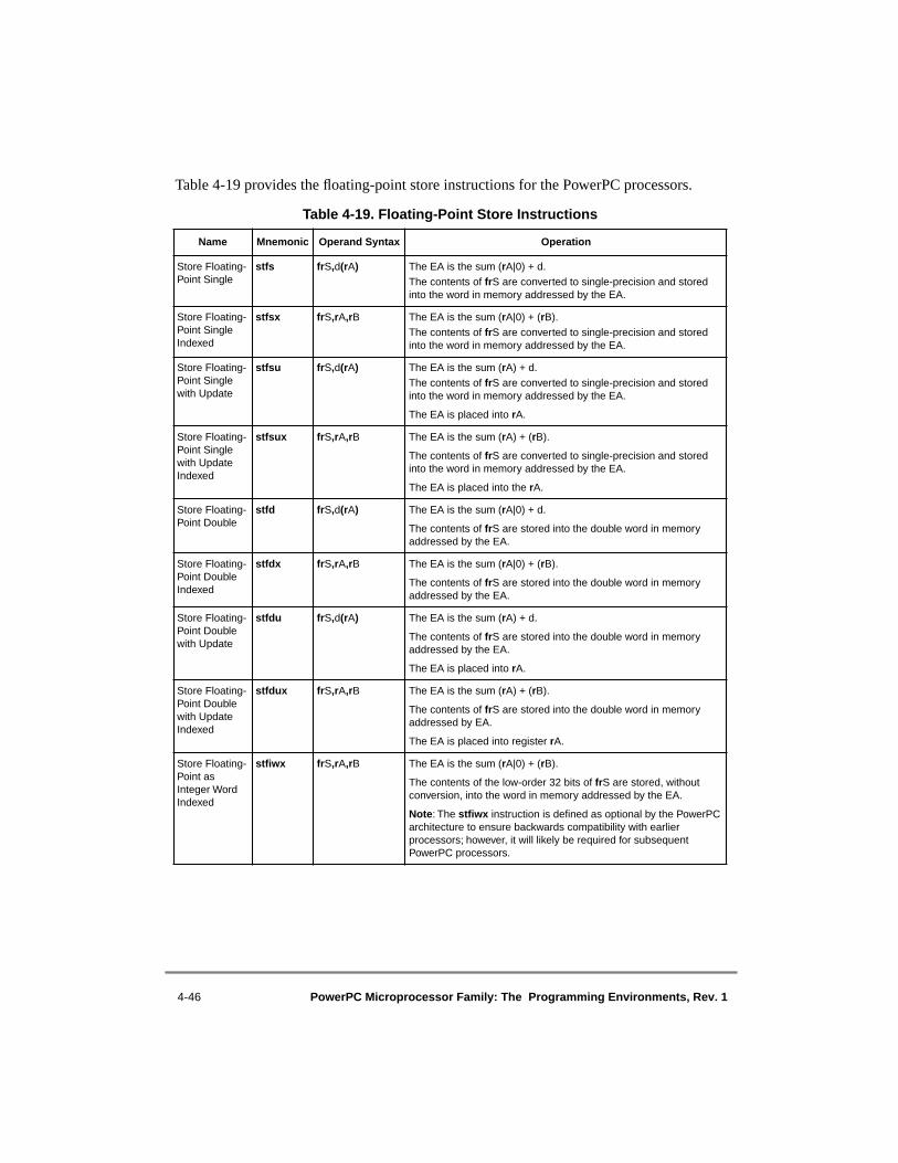
4-46 PowerPC Microprocessor Family: The Programming Environments, Rev. 1
Table 4-19 provides the floating-point store instructions for the PowerPC processors.
Table 4-19. Floating-Point Store Instructions
Name Mnemonic Operand Syntax Operation
Store Floating-Point Single
stfs frS,d(rA) The EA is the sum (rA|0) + d.The contents of frS are converted to single-precision and stored into the word in memory addressed by the EA.
Store Floating-Point Single Indexed
stfsx frS,rA,rB The EA is the sum (rA|0) + (rB).The contents of frS are converted to single-precision and stored into the word in memory addressed by the EA.
Store Floating-Point Single with Update
stfsu frS,d(rA) The EA is the sum (rA) + d.The contents of frS are converted to single-precision and stored into the word in memory addressed by the EA.
The EA is placed into rA.
Store Floating-Point Single with Update Indexed
stfsux frS,rA,rB The EA is the sum (rA) + (rB).
The contents of frS are converted to single-precision and stored into the word in memory addressed by the EA.
The EA is placed into the rA.
Store Floating-Point Double
stfd frS,d(rA) The EA is the sum (rA|0) + d.
The contents of frS are stored into the double word in memory addressed by the EA.
Store Floating-Point Double Indexed
stfdx frS,rA,rB The EA is the sum (rA|0) + (rB).
The contents of frS are stored into the double word in memory addressed by the EA.
Store Floating-Point Double with Update
stfdu frS,d(rA) The EA is the sum (rA) + d.
The contents of frS are stored into the double word in memory addressed by the EA.
The EA is placed into rA.
Store Floating-Point Double with Update Indexed
stfdux frS,rA,rB The EA is the sum (rA) + (rB).
The contents of frS are stored into the double word in memory addressed by EA.
The EA is placed into register rA.
Store Floating-Point as Integer Word Indexed
stfiwx frS,rA,rB The EA is the sum (rA|0) + (rB).
The contents of the low-order 32 bits of frS are stored, without conversion, into the word in memory addressed by the EA.
Note: The stfiwx instruction is defined as optional by the PowerPC architecture to ensure backwards compatibility with earlier processors; however, it will likely be required for subsequent PowerPC processors.

Chapter 4. Addressing Modes and Instruction Set Summary 4-47
4.2.4 Branch and Flow Control InstructionsSome branch instructions can redirect instruction execution conditionally based on thevalue of bits in the CR. When the processor encounters one of these instructions, it scansthe execution pipelines to determine whether an instruction in progress may affect theparticular CR bit. If no interlock is found, the branch can be resolved immediately bychecking the bit in the CR and taking the action defined for the branch instruction.
If an interlock is detected, the branch is considered unresolved and the direction of thebranch may either be predicted using the y bit (as described in Table 4-20) or by usingdynamic prediction. The interlock is monitored while instructions are fetched for thepredicted branch. When the interlock is cleared, the processor determines whether theprediction was correct based on the value of the CR bit. If the prediction is correct, thebranch is considered completed and instruction fetching continues. If the prediction isincorrect, the fetched instructions are purged, and instruction fetching continues along thealternate path.
4.2.4.1 Branch Instruction Address CalculationBranch instructions can alter the sequence of instruction execution. Instruction addressesare always assumed to be word aligned; the PowerPC processors ignore the two low-orderbits of the generated branch target address.
Branch instructions compute the effective address (EA) of the next instruction addressusing the following addressing modes:
• Branch relative • Branch conditional to relative address• Branch to absolute address • Branch conditional to absolute address • Branch conditional to link register • Branch conditional to count register
In the 32-bit mode of a 64-bit implementation, the final step in the address computation isclearing the high-order 32 bits of the target address.
4.2.4.1.1 Branch Relative Addressing ModeInstructions that use branch relative addressing generate the next instruction address bysign extending and appending 0b00 to the immediate displacement operand LI, and addingthe resultant value to the current instruction address. Branches using this addressing modehave the absolute addressing option disabled (AA field, bit 30, in the instructionencoding = 0). The link register (LR) update option can be enabled (LK field, bit 31, in theinstruction encoding = 1). This option causes the effective address of the instructionfollowing the branch instruction to be placed in the LR.

4-48 PowerPC Microprocessor Family: The Programming Environments, Rev. 1
Figure 4-6 shows how the branch target address is generated when using the branch relativeaddressing mode.
Figure 4-6. Branch Relative Addressing
4.2.4.1.2 Branch Conditional to Relative Addressing ModeIf the branch conditions are met, instructions that use the branch conditional to relativeaddressing mode generate the next instruction address by sign extending and appending0b00 to the immediate displacement operand (BD) and adding the resultant value to thecurrent instruction address. Branches using this addressing mode have the absoluteaddressing option disabled (AA field, bit 30, in the instruction encoding = 0). The linkregister update option can be enabled (LK field, bit 31, in the instruction encoding = 1).This option causes the effective address of the instruction following the branch instructionto be placed in the LR.
Figure 4-7 shows how the branch target address is generated when using the branchconditional relative addressing mode.
0 5 6 29 30 31
18 LI AA LK
0 63
Branch Target Address
Instruction Encoding:
+0 63
Current Instruction Address
0 37 38 61 62 63
LI 0 0Sign Extension
Reserved
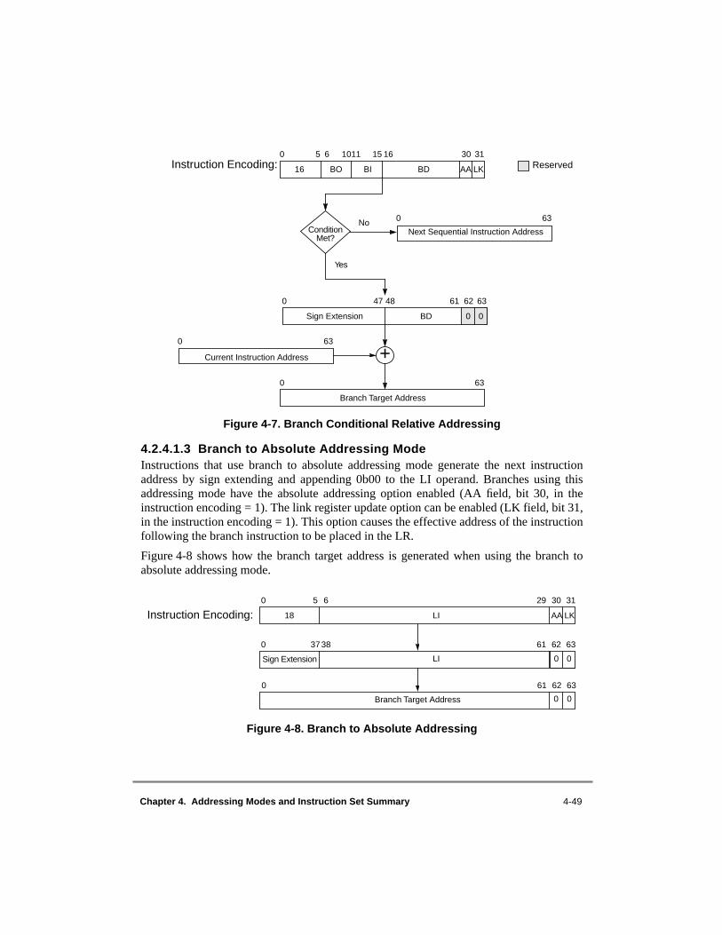
Chapter 4. Addressing Modes and Instruction Set Summary 4-49
Figure 4-7. Branch Conditional Relative Addressing
4.2.4.1.3 Branch to Absolute Addressing ModeInstructions that use branch to absolute addressing mode generate the next instructionaddress by sign extending and appending 0b00 to the LI operand. Branches using thisaddressing mode have the absolute addressing option enabled (AA field, bit 30, in theinstruction encoding = 1). The link register update option can be enabled (LK field, bit 31,in the instruction encoding = 1). This option causes the effective address of the instructionfollowing the branch instruction to be placed in the LR.
Figure 4-8 shows how the branch target address is generated when using the branch toabsolute addressing mode.
Figure 4-8. Branch to Absolute Addressing
0 5 6 1011 15 16 30 31
16 BO BI BD AA LK
Yes
0 63
Branch Target Address
Instruction Encoding:
No
+0 63
Current Instruction Address
0 63
Next Sequential Instruction Address
0 47 48 61 62 63
Sign Extension BD 0 0
Condition Met?
Reserved
0 5 6 29 30 31
18 LI AA LK
0 3738 61 62 63
0 61 62 63
Branch Target Address
Instruction Encoding:
LI 0 0Sign Extension
0 0

4-50 PowerPC Microprocessor Family: The Programming Environments, Rev. 1
4.2.4.1.4 Branch Conditional to Absolute Addressing ModeIf the branch conditions are met, instructions that use the branch conditional to absoluteaddressing mode generate the next instruction address by sign extending and appending0b00 to the BD operand. Branches using this addressing mode have the absolute addressingoption enabled (AA field, bit 30, in the instruction encoding = 1). The link register updateoption can be enabled (LK field, bit 31, in the instruction encoding = 1). This option causesthe effective address of the instruction following the branch instruction to be placed in theLR.
Figure 4-9 shows how the branch target address is generated when using the branchconditional to absolute addressing mode.
Figure 4-9. Branch Conditional to Absolute Addressing
4.2.4.1.5 Branch Conditional to Link Register Addressing ModeIf the branch conditions are met, the branch conditional to link register instruction generatesthe next instruction address by fetching the contents of the LR and clearing the two low-order bits to zero. The link register update option can be enabled (LK field, bit 31, in theinstruction encoding = 1). This option causes the effective address of the instructionfollowing the branch instruction to be placed in the LR.
Figure 4-10 shows how the branch target address is generated when using the branchconditional to link register addressing mode.
0 5 6 1011 15 16 29 30 31
16 BO BI BD AA LK
0 47 48 61 62 63
0 61 62 63
Branch Target Address
Instruction Encoding:
No0 63
Next Sequential Instruction Address
Sign Extension BD 0 0
Condition Met?
Yes
0 0

Chapter 4. Addressing Modes and Instruction Set Summary 4-51
Figure 4-10. Branch Conditional to Link Register Addressing
4.2.4.1.6 Branch Conditional to Count Register Addressing ModeIf the branch conditions are met, the branch conditional to count register instructiongenerates the next instruction address by fetching the contents of the count register (CTR)and clearing the two low-order bits to zero. The link register update option can be enabled(LK field, bit 31, in the instruction encoding = 1). This option causes the effective addressof the instruction following the branch instruction to be placed in the LR.
Figure 4-11 shows how the branch target address is generated when using the branchconditional to count register addressing mode.
0 5 6 10 11 15 16 20 21 30 31
Condition Met?
0 0
62 63
LR
0 61
0 63
Branch Target Address
Instruction Encoding:
No0 63
Next Sequential Instruction Address
Yes
19 BO BI 0 0 0 0 0 16 LK
||
Reserved

4-52 PowerPC Microprocessor Family: The Programming Environments, Rev. 1
Figure 4-11. Branch Conditional to Count Register Addressing
4.2.4.2 Conditional Branch ControlFor branch conditional instructions, the BO operand specifies the conditions under whichthe branch is taken. The first four bits of the BO operand specify how the branch is affectedby or affects the condition and count registers. The fifth bit, shown in Table 4-20 as havingthe value y, is used by some PowerPC implementations for branch prediction as describedbelow.
The encodings for the BO operands are shown in Table 4-20. M = 32 in 32-bit mode (of a64-bit implementation) and M = 0 in the default 64-bit mode. If the BO field specifies thatthe CTR is to be decremented, the entire 64-bit CTR is decremented regardless of the 32-bitmode or the default 64-bit mode.
Table 4-20. BO Operand Encodings
BO Description
0000y Decrement the CTR, then branch if the decremented CTR[M–63] ≠ 0 and the condition is FALSE.
0001y Decrement the CTR, then branch if the decremented CTR[M–63] = 0 and the condition is FALSE.
001zy Branch if the condition is FALSE.
0100y Decrement the CTR, then branch if the decremented CTR[M–63] ≠ 0 and the condition is TRUE.
0101y Decrement the CTR, then branch if the decremented CTR[M–63] = 0 and the condition is TRUE.
011zy Branch if the condition is TRUE.
1z00y Decrement the CTR, then branch if the decremented CTR[M–63] ≠ 0.
0 0
62 63
CTR
0 61
0 63
Branch Target Address
Instruction Encoding:
Condition Met?
No
Yes
0 63
Next Sequential Instruction Address
0 5 6 1011 15 16 20 21 30 31
19 BO BI 00000 528 LK
||
Reserved

Chapter 4. Addressing Modes and Instruction Set Summary 4-53
The branch always encoding of the BO operand does not have a y bit.
Clearing the y bit indicates a predicted behavior for the branch instruction as follows:
• For bcx with a negative value in the displacement operand, the branch is taken.
• In all other cases (bcx with a non-negative value in the displacement operand, bclrx, or bcctrx), the branch is not taken.
Setting the y bit reverses the preceding indications.
The sign of the displacement operand is used as described above even if the target is anabsolute address. The default value for the y bit should be 0, and should only be set to 1 ifsoftware has determined that the prediction corresponding to y = 1 is more likely to becorrect than the prediction corresponding to y = 0. Software that does not compute branchpredictions should clear the y bit.
In most cases, the branch should be predicted to be taken if the value of the followingexpression is 1, and predicted to fall through if the value is 0.
((BO[0] & BO[2]) | S) ≈ BO[4]
In the expression above, S (bit 16 of the branch conditional instruction coding) is the signbit of the displacement operand if the instruction has a displacement operand and is 0 if theoperand is reserved. BO[4] is the y bit, or 0 for the branch always encoding of the BOoperand. (Advantage is taken of the fact that, for bclrx and bcctrx, bit 16 of the instructionis part of a reserved operand and therefore must be 0.)
The 5-bit BI operand in branch conditional instructions specifies which of the 32 bits in theCR represents the condition to test.
When the branch instructions contain immediate addressing operands, the target addressescan be computed sufficiently ahead of the branch instruction that instructions can befetched along the target path. If the branch instructions use the link and count registers,instructions along the target path can be fetched if the link or count register is loadedsufficiently ahead of the branch instruction.
1z01y Decrement the CTR, then branch if the decremented CTR[M–63] = 0.
1z1zz Branch always.
In this table, z indicates a bit that is ignored. Note that the z bits should be cleared, as they may be assigned a meaning in some future version of the PowerPC architecture.
The y bit provides a hint about whether a conditional branch is likely to be taken, and may be used by some PowerPC implementations to improve performance.
Table 4-20. BO Operand Encodings (Continued)
BO Description
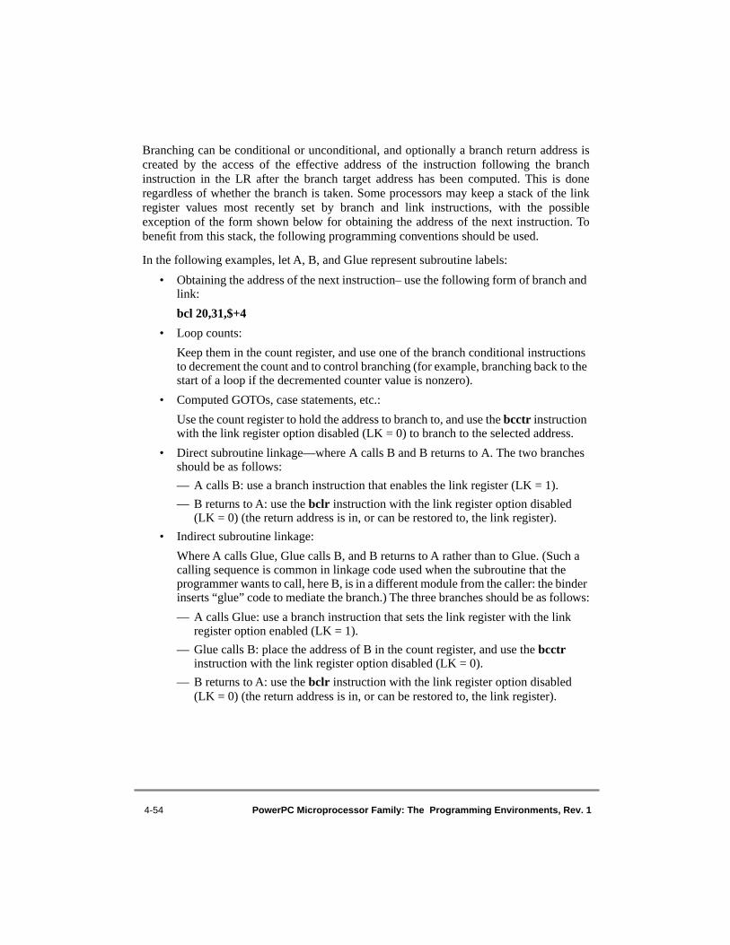
4-54 PowerPC Microprocessor Family: The Programming Environments, Rev. 1
Branching can be conditional or unconditional, and optionally a branch return address iscreated by the access of the effective address of the instruction following the branchinstruction in the LR after the branch target address has been computed. This is doneregardless of whether the branch is taken. Some processors may keep a stack of the linkregister values most recently set by branch and link instructions, with the possibleexception of the form shown below for obtaining the address of the next instruction. Tobenefit from this stack, the following programming conventions should be used.
In the following examples, let A, B, and Glue represent subroutine labels:
• Obtaining the address of the next instruction– use the following form of branch and link:
bcl 20,31,$+4
• Loop counts:
Keep them in the count register, and use one of the branch conditional instructions to decrement the count and to control branching (for example, branching back to the start of a loop if the decremented counter value is nonzero).
• Computed GOTOs, case statements, etc.:
Use the count register to hold the address to branch to, and use the bcctr instruction with the link register option disabled (LK = 0) to branch to the selected address.
• Direct subroutine linkage—where A calls B and B returns to A. The two branches should be as follows:
— A calls B: use a branch instruction that enables the link register (LK = 1).
— B returns to A: use the bclr instruction with the link register option disabled (LK = 0) (the return address is in, or can be restored to, the link register).
• Indirect subroutine linkage:
Where A calls Glue, Glue calls B, and B returns to A rather than to Glue. (Such a calling sequence is common in linkage code used when the subroutine that the programmer wants to call, here B, is in a different module from the caller: the binder inserts “glue” code to mediate the branch.) The three branches should be as follows:
— A calls Glue: use a branch instruction that sets the link register with the link register option enabled (LK = 1).
— Glue calls B: place the address of B in the count register, and use the bcctr instruction with the link register option disabled (LK = 0).
— B returns to A: use the bclr instruction with the link register option disabled (LK = 0) (the return address is in, or can be restored to, the link register).

Chapter 4. Addressing Modes and Instruction Set Summary 4-55
4.2.4.3 Branch InstructionsTable 4-21 describes the branch instructions provided by the PowerPC processors.
Table 4-21. Branch Instructions
Name Mnemonic Operand Syntax Operation
Branch bbablbla
target_addr b Branch. Branch to the address computed as the sum of the immediate address and the address of the current instruction.
ba Branch Absolute. Branch to the absolute address specified.bl Branch then Link. Branch to the address computed as the sum
of the immediate address and the address of the current instruction. The instruction address following this instruction is placed into the link register (LR).
bla Branch Absolute then Link. Branch to the absolute address specified. The instruction address following this instruction is placed into the LR.
Branch Conditional
bcbcabclbcla
BO,BI,target_addr The BI operand specifies the bit in the CR to be used as the condition of the branch. The BO operand is used as described in Table 4-20.
bc Branch Conditional. Branch conditionally to the address computed as the sum of the immediate address and the address of the current instruction.
bca Branch Conditional Absolute. Branch conditionally to the absolute address specified.
bcl Branch Conditional then Link. Branch conditionally to the address computed as the sum of the immediate address and the address of the current instruction. The instruction address following this instruction is placed into the LR.
bcla Branch Conditional Absolute then Link. Branch conditionally to the absolute address specified. The instruction address following this instruction is placed into the LR.
Branch Conditional to Link Register
bclrbclrl
BO,BI The BI operand specifies the bit in the CR to be used as the condition of the branch. The BO operand is used as described in Table 4-20, and the branch target address is LR[0–61] || 0b00, with the high-order 32 bits of the branch target address cleared in the 32-bit mode of a 64-bit implementation.
bclr Branch Conditional to Link Register. Branch conditionally to the address in the LR.
bclrl Branch Conditional to Link Register then Link. Branch conditionally to the address specified in the LR. The instruction address following this instruction is then placed into the LR.
Branch Conditional to Count Register
bcctrbcctrl
BO,BI The BI operand specifies the bit in the CR to be used as the condition of the branch. The BO operand is used as described in Table 4-20, and the branch target address is CTR[0–61] || 0b00, with the high-order 32 bits of the branch target address cleared in the 32-bit mode of a 64-bit implementation.
bcctr Branch Conditional to Count Register. Branch conditionally to the address specified in the count register.
bcctrl Branch Conditional to Count Register then Link. Branch conditionally to the address specified in the count register. The instruction address following this instruction is placed into the LR.
Note: If the “decrement and test CTR” option is specified (BO[2] = 0), the instruction form is invalid.

4-56 PowerPC Microprocessor Family: The Programming Environments, Rev. 1
4.2.4.4 Simplified Mnemonics for Branch Processor InstructionsTo simplify assembly language programming, a set of simplified mnemonics and symbolsis provided for the most frequently used forms of branch conditional, compare, trap, rotateand shift, and certain other instructions. See Appendix F, “Simplified Mnemonics,” for alist of simplified mnemonic examples.
4.2.4.5 Condition Register Logical InstructionsCondition register logical instructions, shown in Table 4-22, and the Move ConditionRegister Field (mcrf) instruction are also defined as flow control instructions.
Note that if the LR update option is enabled for any of these instructions, the PowerPCarchitecture defines these forms of the instructions as invalid.
Table 4-22. Condition Register Logical Instructions
Name Mnemonic Operand Syntax Operation
Condition Register AND
crand crbD,crbA,crbB The CR bit specified by crbA is ANDed with the CR bit specified by crbB. The result is placed into the CR bit specified by crbD.
Condition Register OR
cror crbD,crbA,crbB The CR bit specified by crbA is ORed with the CR bit specified by crbB. The result is placed into the CR bit specified by crbD.
Condition Register XOR
crxor crbD,crbA,crbB The CR bit specified by crbA is XORed with the CR bit specified by crbB. The result is placed into the CR bit specified by crbD.
Condition Register NAND
crnand crbD,crbA,crbB The CR bit specified by crbA is ANDed with the CR bit specified by crbB. The complemented result is placed into the CR bit specified by crbD.
Condition Register NOR
crnor crbD,crbA,crbB The CR bit specified by crbA is ORed with the CR bit specified by crbB. The complemented result is placed into the CR bit specified by crbD.
Condition Register Equivalent
creqv crbD,crbA, crbB The CR bit specified by crbA is XORed with the CR bit specified by crbB. The complemented result is placed into the CR bit specified by crbD.
Condition Register AND with Complement
crandc crbD,crbA, crbB The CR bit specified by crbA is ANDed with the complement of the CR bit specified by crbB and the result is placed into the CR bit specified by crbD.
Condition Register OR with Complement
crorc crbD,crbA, crbB The CR bit specified by crbA is ORed with the complement of the CR bit specified by crbB and the result is placed into the CR bit specified by crbD.
Move Condition Register Field
mcrf crfD,crfS The contents of crfS are copied into crfD. No other condition register fields are changed.
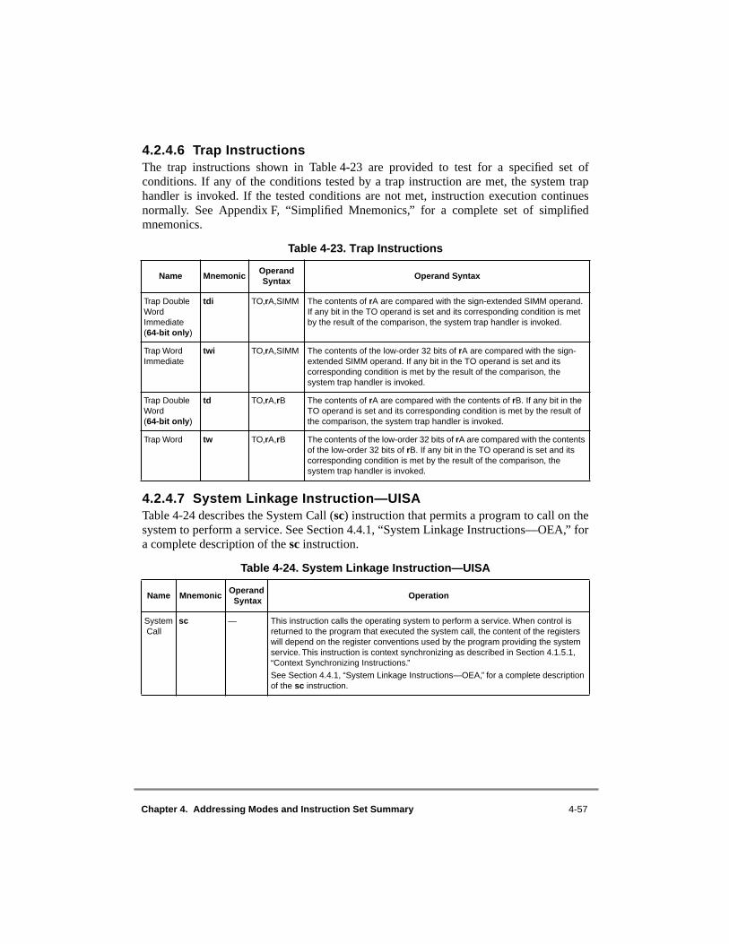
Chapter 4. Addressing Modes and Instruction Set Summary 4-57
4.2.4.6 Trap InstructionsThe trap instructions shown in Table 4-23 are provided to test for a specified set ofconditions. If any of the conditions tested by a trap instruction are met, the system traphandler is invoked. If the tested conditions are not met, instruction execution continuesnormally. See Appendix F, “Simplified Mnemonics,” for a complete set of simplifiedmnemonics.
4.2.4.7 System Linkage Instruction—UISATable 4-24 describes the System Call (sc) instruction that permits a program to call on thesystem to perform a service. See Section 4.4.1, “System Linkage Instructions—OEA,” fora complete description of the sc instruction.
Table 4-23. Trap Instructions
Name MnemonicOperand Syntax
Operand Syntax
Trap Double Word Immediate(64-bit only)
tdi TO,rA,SIMM The contents of rA are compared with the sign-extended SIMM operand. If any bit in the TO operand is set and its corresponding condition is met by the result of the comparison, the system trap handler is invoked.
Trap Word Immediate
twi TO,rA,SIMM The contents of the low-order 32 bits of rA are compared with the sign-extended SIMM operand. If any bit in the TO operand is set and its corresponding condition is met by the result of the comparison, the system trap handler is invoked.
Trap Double Word(64-bit only)
td TO,rA,rB The contents of rA are compared with the contents of rB. If any bit in the TO operand is set and its corresponding condition is met by the result of the comparison, the system trap handler is invoked.
Trap Word tw TO,rA,rB The contents of the low-order 32 bits of rA are compared with the contents of the low-order 32 bits of rB. If any bit in the TO operand is set and its corresponding condition is met by the result of the comparison, the system trap handler is invoked.
Table 4-24. System Linkage Instruction—UISA
Name MnemonicOperand Syntax
Operation
System Call
sc — This instruction calls the operating system to perform a service. When control is returned to the program that executed the system call, the content of the registers will depend on the register conventions used by the program providing the system service. This instruction is context synchronizing as described in Section 4.1.5.1, “Context Synchronizing Instructions.”See Section 4.4.1, “System Linkage Instructions—OEA,” for a complete description of the sc instruction.

4-58 PowerPC Microprocessor Family: The Programming Environments, Rev. 1
4.2.5 Processor Control Instructions—UISAProcessor control instructions are used to read from and write to the condition register(CR), machine state register (MSR), and special-purpose registers (SPRs). SeeSection 4.3.1, “Processor Control Instructions—VEA,” for the mftb instruction andSection 4.4.2, “Processor Control Instructions—OEA,” for information about theinstructions used for reading from and writing to the MSR and SPRs.
4.2.5.1 Move to/from Condition Register InstructionsTable 4-25 summarizes the instructions for reading from or writing to the condition register.
4.2.5.2 Move to/from Special-Purpose Register Instructions (UISA)Table 4-26 provides a brief description of the mtspr and mfspr instructions. For moredetailed information refer to Chapter 8, “Instruction Set.”
Table 4-25. Move to/from Condition Register Instructions
Name MnemonicOperand Syntax
Operation
Move to Condition Register Fields
mtcrf CRM,rS The contents of the low-order 32 bits of rS are placed into the CR under control of the field mask specified by operand CRM. The field mask identifies the 4-bit fields affected. Let i be an integer in the range 0–7. If CRM(i) = 1, CR field i (CR bits 4 * i through 4 * i + 3) is set to the contents of the corresponding field of the low-order 32 bits of rS.
Move to Condition Register from XER
mcrxr crfD The contents of XER[0–3] are copied into the condition register field designated by crfD. All other CR fields remain unchanged. The contents of XER[0–3] are cleared.
Move from Condition Register
mfcr rD The contents of the CR are placed into the low-order 32 bits of rD. The contents of the high-order 32 bits of rD are cleared in 64-bit implementations.
Table 4-26. Move to/from Special-Purpose Register Instructions (UISA)
Name MnemonicOperand Syntax
Operation
Move to Special-Purpose Register
mtspr SPR,rS The value specified by rS are placed in the specified SPR. For 32-bit SPRs, the low-order 32 bits of rS are placed into the SPR.
Move from Special-Purpose Register
mfspr rD,SPR The contents of the specified SPR are placed in rD. For 32-bit SPRs, the low-order 32 bits of rD receive the contents of the SPR. The high-order 32 bits of rD are cleared.
U
V
O
U
Chapter 4. Addressing Modes and Instruction Set Summary 4-59
4.2.6 Memory Synchronization Instructions—UISAMemory synchronization instructions control the order in which memory operations arecompleted with respect to asynchronous events, and the order in which memory operationsare seen by other processors or memory access mechanisms.
The number of cycles required to complete a sync instruction depends on systemparameters and on the processor's state when the instruction is issued. As a result, frequentuse of this instruction may degrade performance slightly. The eieio instruction may be moreappropriate than sync for many cases.
The PowerPC architecture defines the sync instruction with CR update enabled (Rc field,bit 31 = 1) to be an invalid form.
The proper paired use of the lwarx with stwcx. and ldarx with stdcx. instructions allowsprogrammers to emulate common semaphore operations such as test and set, compare andswap, exchange memory, and fetch and add. Examples of these semaphore operations canbe found in Appendix E, “Synchronization Programming Examples.” The lwarxinstruction must be paired with an stwcx. instruction, and ldarx instruction with an stdcx.instruction, with the same effective address specified by both instructions of the pair. Theonly exception is that an unpaired stwcx. or stdcx. instruction to any (scratch) effectiveaddress can be used to clear any reservation held by the processor. Note that the reservationgranularity is implementation-dependent.
The concept behind the use of the lwarx, ldarx, stwcx., and stdcx. instructions is that aprocessor may load a semaphore from memory, compute a result based on the value of thesemaphore, and conditionally store it back to the same location. The conditional store isperformed based upon the existence of a reservation established by the preceding lwarx orldarx instruction. If the reservation exists when the store is executed, the store is performedand a bit is set in the CR. If the reservation does not exist when the store is executed, thetarget memory location is not modified and a bit is cleared in the CR.
The lwarx, ldarx, stwcx., and stdcx. primitives allow software to read a semaphore,compute a result based on the value of the semaphore, store the new value back into thesemaphore location only if that location has not been modified since it was first read, anddetermine if the store was successful. If the store was successful, the sequence ofinstructions from the read of the semaphore to the store that updated the semaphore appearto have been executed atomically (that is, no other processor or mechanism modified thesemaphore location between the read and the update), thus providing the equivalent of areal atomic operation. However, in reality, other processors may have read from the locationduring this operation.
The lwarx, ldarx, stwcx., and stdcx. instructions require the EA to be aligned.
In general, the lwarx, ldarx, stwcx., and stdcx. instructions should be used only in systemprograms, which can be invoked by application programs as needed.
U
V

4-60 PowerPC Microprocessor Family: The Programming Environments, Rev. 1
At most one reservation exists simultaneously on any processor. The address associatedwith the reservation can be changed by a subsequent lwarx or ldarx instruction. Theconditional store is performed based upon the existence of a reservation established by thepreceding lwarx or ldarx. instruction.
A reservation held by the processor is cleared (or may be cleared, in the case of the fourthand fifth bullet items) by one of the following:
• The processor holding the reservation executes another lwarx or ldarx instruction; this clears the first reservation and establishes a new one.
• The processor holding the reservation executes any stwcx. or stdcx. instruction whether its address matches that of the lwarx.
• Some other processor executes a store or dcbz to the same reservation granule, or modifies a referenced or changed bit in the same reservation granule.
• Some other processor executes a dcbtst, dcbst, dcbf, or dcbi to the same reservation granule; whether the reservation is cleared is undefined.
• Some other processor executes a dcba to the same reservation granule. The reservation is cleared if the instruction causes the target block to be newly established in the data cache or to be modified; otherwise, whether the reservation is cleared is undefined.
• Some other mechanism modifies a memory location in the same reservation granule.
Note that exceptions do not clear reservations; however, system software invoked by exceptions may clear reservations.
Table 4-27 summarizes the memory synchronization instructions as defined in the UISA.See Section 4.3.2, “Memory Synchronization Instructions—VEA,” for details aboutadditional memory synchronization (eieio and isync) instructions.
Table 4-27. Memory Synchronization Instructions—UISA
Name MnemonicOperand Syntax
Operation
Load Double Word and Reserve Indexed(64-bit only)
ldarx rD,rA,rB The EA is the sum (rA|0) + (rB). The double word in memory addressed by the EA is loaded into rD.
Load Word and Reserve Indexed
lwarx rD,rA,rB The EA is the sum (rA|0) + (rB). The word in memory addressed by the EA is loaded into the low-order 32 bits of rD. The contents of the high-order 32 bits of rD are cleared for 64-bit implementations.
U

Chapter 4. Addressing Modes and Instruction Set Summary 4-61
4.2.7 Recommended Simplified MnemonicsTo simplify assembly language programs, a set of simplified mnemonics is provided forsome of the most frequently used operations (such as no-op, load immediate, load address,move register, and complement register). Assemblers should provide the simplifiedmnemonics listed in Section F.9, “Recommended Simplified Mnemonics.” Programswritten to be portable across the various assemblers for the PowerPC architecture shouldnot assume the existence of mnemonics not described in this document.
For a complete list of simplified mnemonics, see Appendix F, “Simplified Mnemonics.”
Store Double Word Conditional Indexed(64-bit only)
stdcx. rS,rA,rB The EA is the sum (rA|0) + (rB).
If a reservation exists and the effective address specified by the stdcx. instruction is the same as that specified by the load and reserve instruction that established the reservation, the contents of rS are stored into the double word in memory addressed by the EA, and the reservation is cleared.
If a reservation exists but the effective address specified by the stdcx. instruction is not the same as that specified by the load and reserve instruction that established the reservation, the reservation is cleared, and it is undefined whether the contents of rS are stored into the double word in memory addressed by the EA.
If a reservation does not exist, the instruction completes without altering memory or the contents of the cache.
Store Word Conditional Indexed
stwcx. rS,rA,rB The EA is the sum (rA|0) + (rB).
If a reservation exists and the effective address specified by the stwcx. instruction is the same as that specified by the load and reserve instruction that established the reservation, the low-order 32 bits of rS are stored into the word in memory addressed by the EA, and the reservation is cleared.
If a reservation exists but the effective address specified by the stwcx. instruction is not the same as that specified by the load and reserve instruction that established the reservation, the reservation is cleared, and it is undefined whether the low-order 32 bits of rS are stored into the word in memory addressed by the EA.
If a reservation does not exist, the instruction completes without altering memory or the contents of the cache.
Synchronize sync — Executing a sync instruction ensures that all instructions preceding the sync instruction appear to have completed before the sync instruction completes, and that no subsequent instructions are initiated by the processor until after the sync instruction completes. When the sync instruction completes, all memory accesses caused by instructions preceding the sync instruction will have been performed with respect to all other mechanisms that access memory.
See Chapter 8, “Instruction Set,” for more information.
Table 4-27. Memory Synchronization Instructions—UISA (Continued)
Name MnemonicOperand Syntax
Operation

4-62 PowerPC Microprocessor Family: The Programming Environments, Rev. 1
4.3 PowerPC VEA InstructionsThe PowerPC virtual environment architecture (VEA) describes the semantics of thememory model that can be assumed by software processes, and includes descriptions of thecache model, cache-control instructions, address aliasing, and other related issues.Implementations that conform to the VEA also adhere to the UISA, but may not necessarilyadhere to the OEA.
This section describes additional instructions that are provided by the VEA.
4.3.1 Processor Control Instructions—VEAThe VEA defines the mftb instruction (user-level instruction) for reading the contents ofthe time base register; see Chapter 5, “Cache Model and Memory Coherency,” for moreinformation. Table 4-28 describes the mftb instruction.
Simplified mnemonics are provided (See Section F.8, “Simplified Mnemonics for Special-Purpose Registers”) for the mftb instruction so it can be coded with the TBR name as partof the mnemonic rather than requiring it to be coded as an operand. The simplifiedmnemonics Move from Time Base (mftb) and Move from Time Base Upper (mftbu) arevariants of the mftb instruction rather than of the mfspr instruction. The mftb instructionserves as both a basic and simplified mnemonic. Assemblers recognize an mftb mnemonicwith two operands as the basic form, and an mftb mnemonic with one operand as thesimplified form.
On 32-bit implementations, it is not possible to read the entire 64-bit time base register ina single instruction. The mftb simplified mnemonic moves from the lower half of the timebase register (TBL) to a GPR, and the mftbu simplified mnemonic moves from the upperhalf of the time base (TBU) to a GPR.
Table 4-29 summarizes the time base (TBL/TBU) register encodings to which user-levelaccess (using mftb) is permitted (as specified by the VEA).
Table 4-28. Move from Time Base Instruction
Name Mnemonic Operand Syntax Operation
Move from Time Base
mftb rD, TBR The TBR field denotes either time base lower or time base upper, encoded as shown in Table 4-29 and Table 4-30. The contents of the designated register are copied to rD. When reading TBU on a 64-bit implementation, the high-order 32 bits of rD are cleared. When reading TBL on a 64-bit implementation, the 64 bits of the time base are copied to rD.
Table 4-29. User-Level TBR Encodings (VEA)
Decimal Value in TBR Field
tbr[0–4] tbr[5–9]Register
NameDescription
268 01100 01000 TBL Time base lower (read-only)
269 01101 01000 TBU Time base upper (read-only)
U
V
O
V
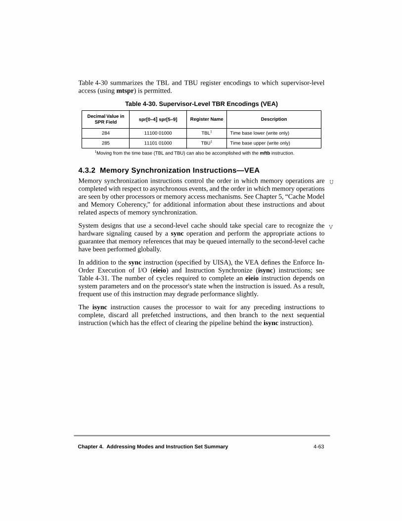
Chapter 4. Addressing Modes and Instruction Set Summary 4-63
Table 4-30 summarizes the TBL and TBU register encodings to which supervisor-levelaccess (using mtspr) is permitted.
4.3.2 Memory Synchronization Instructions—VEAMemory synchronization instructions control the order in which memory operations arecompleted with respect to asynchronous events, and the order in which memory operationsare seen by other processors or memory access mechanisms. See Chapter 5, “Cache Modeland Memory Coherency,” for additional information about these instructions and aboutrelated aspects of memory synchronization.
System designs that use a second-level cache should take special care to recognize thehardware signaling caused by a sync operation and perform the appropriate actions toguarantee that memory references that may be queued internally to the second-level cachehave been performed globally.
In addition to the sync instruction (specified by UISA), the VEA defines the Enforce In-Order Execution of I/O (eieio) and Instruction Synchronize (isync) instructions; seeTable 4-31. The number of cycles required to complete an eieio instruction depends onsystem parameters and on the processor's state when the instruction is issued. As a result,frequent use of this instruction may degrade performance slightly.
The isync instruction causes the processor to wait for any preceding instructions tocomplete, discard all prefetched instructions, and then branch to the next sequentialinstruction (which has the effect of clearing the pipeline behind the isync instruction).
Table 4-30. Supervisor-Level TBR Encodings (VEA)
Decimal Value in SPR Field spr[0–4] spr[5–9] Register Name Description
284 11100 01000 TBL1 Time base lower (write only)
285 11101 01000 TBU1 Time base upper (write only)
1Moving from the time base (TBL and TBU) can also be accomplished with the mftb instruction.
U
V
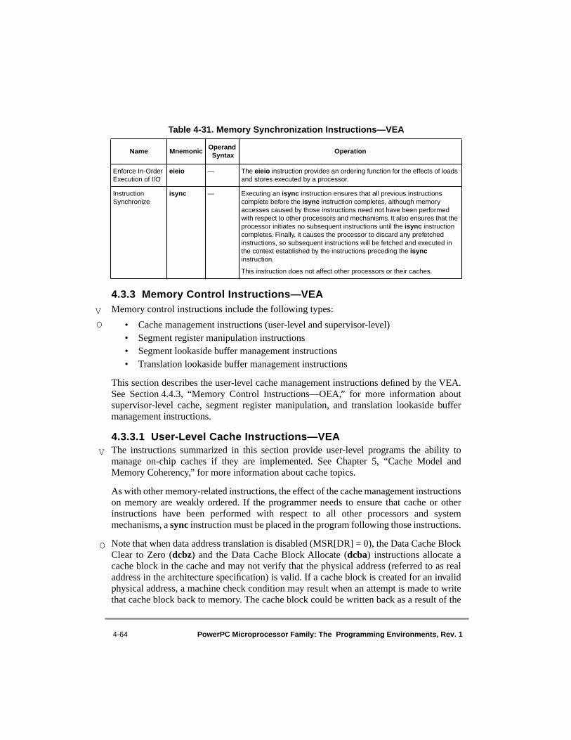
4-64 PowerPC Microprocessor Family: The Programming Environments, Rev. 1
4.3.3 Memory Control Instructions—VEAMemory control instructions include the following types:
• Cache management instructions (user-level and supervisor-level)• Segment register manipulation instructions• Segment lookaside buffer management instructions• Translation lookaside buffer management instructions
This section describes the user-level cache management instructions defined by the VEA.See Section 4.4.3, “Memory Control Instructions—OEA,” for more information aboutsupervisor-level cache, segment register manipulation, and translation lookaside buffermanagement instructions.
4.3.3.1 User-Level Cache Instructions—VEAThe instructions summarized in this section provide user-level programs the ability tomanage on-chip caches if they are implemented. See Chapter 5, “Cache Model andMemory Coherency,” for more information about cache topics.
As with other memory-related instructions, the effect of the cache management instructionson memory are weakly ordered. If the programmer needs to ensure that cache or otherinstructions have been performed with respect to all other processors and systemmechanisms, a sync instruction must be placed in the program following those instructions.
Note that when data address translation is disabled (MSR[DR] = 0), the Data Cache BlockClear to Zero (dcbz) and the Data Cache Block Allocate (dcba) instructions allocate acache block in the cache and may not verify that the physical address (referred to as realaddress in the architecture specification) is valid. If a cache block is created for an invalidphysical address, a machine check condition may result when an attempt is made to writethat cache block back to memory. The cache block could be written back as a result of the
Table 4-31. Memory Synchronization Instructions—VEA
Name MnemonicOperand Syntax
Operation
Enforce In-Order Execution of I/O
eieio — The eieio instruction provides an ordering function for the effects of loads and stores executed by a processor.
Instruction Synchronize
isync — Executing an isync instruction ensures that all previous instructions complete before the isync instruction completes, although memory accesses caused by those instructions need not have been performed with respect to other processors and mechanisms. It also ensures that the processor initiates no subsequent instructions until the isync instruction completes. Finally, it causes the processor to discard any prefetched instructions, so subsequent instructions will be fetched and executed in the context established by the instructions preceding the isync instruction.
This instruction does not affect other processors or their caches.
V
O
V
O

Chapter 4. Addressing Modes and Instruction Set Summary 4-65
execution of an instruction that causes a cache miss and the invalid addressed cache blockis the target for replacement or a Data Cache Block Store (dcbst) instruction.
Any cache control instruction that generates an effective address that corresponds to adirect-store segment (segment descriptor[T] = 1) is treated as a no-op. However, note thatthe direct-store facility is being phased out of the architecture and will not likely besupported in future devices.
Table 4-32 summarizes the cache instructions defined by the VEA. Note that theseinstructions are accessible to user-level programs.
Table 4-32. User-Level Cache Instructions
Name MnemonicOperand Syntax
Operation
Data Cache Block Touch
dcbt rA,rB The EA is the sum (rA|0) + (rB).
This instruction is a hint that performance will probably be improved if the block containing the byte addressed by EA is fetched into the data cache, because the program will probably soon load from the addressed byte.
Data Cache Block Touch for Store
dcbtst rA,rB The EA is the sum (rA|0) + (rB).
This instruction is a hint that performance will probably be improved if the block containing the byte addressed by EA is fetched into the data cache, because the program will probably soon store into the addressed byte.
Data Cache Block Allocate
dcba rA,rB The EA is the sum (rA|0) + (rB).
If the cache block containing the byte addressed by the EA is in the data cache, all bytes of the cache block are made undefined, but the cache block is still considered valid. Note that programming errors can occur if the data in this cache block is subsequently read or used inadvertently.
If the page containing the byte addressed by the EA is not in the data cache and the corresponding page is marked caching allowed (I = 0), the cache block is allocated (and made valid) in the data cache without fetching the block from main memory, and the value of all bytes of the cache block is undefined.
If the page containing the byte addressed by the EA is marked caching inhibited (WIM = x1x), this instruction is treated as a no-op.
If the cache block addressed by the EA is located in a page marked as memory coherent (WIM = xx1) and the cache block exists in the caches of other processors, memory coherence is maintained in those caches.
The dcba instruction is treated as a store to the addressed byte with respect to address translation, memory protection, referenced and changed recording, and the ordering enforced by eieio or by the combination of caching-inhibited and guarded attributes for a page.
This instruction is optional in the PowerPC architecture.
(In the PowerPC OEA, the dcba instruction is additionally defined to clear all bytes of a newly established block to zero in the case that the block did not already exist in the cache.)
V
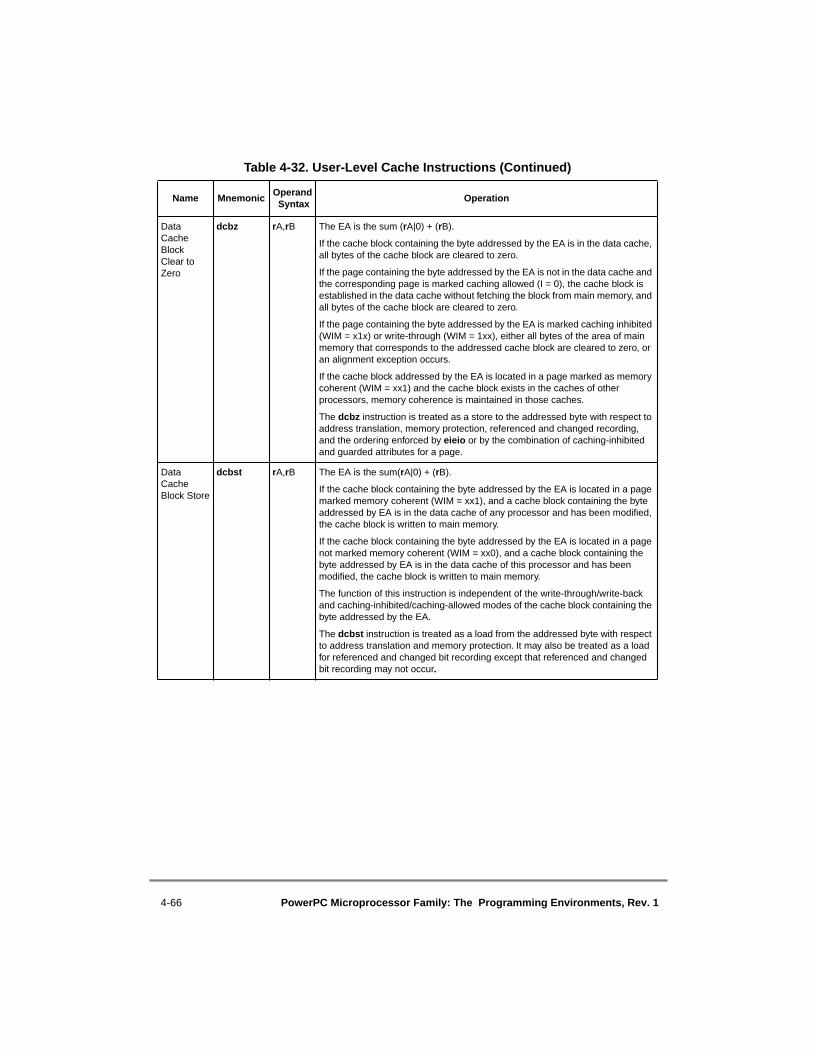
4-66 PowerPC Microprocessor Family: The Programming Environments, Rev. 1
Data Cache Block Clear to Zero
dcbz rA,rB The EA is the sum (rA|0) + (rB).
If the cache block containing the byte addressed by the EA is in the data cache, all bytes of the cache block are cleared to zero.
If the page containing the byte addressed by the EA is not in the data cache and the corresponding page is marked caching allowed (I = 0), the cache block is established in the data cache without fetching the block from main memory, and all bytes of the cache block are cleared to zero.
If the page containing the byte addressed by the EA is marked caching inhibited (WIM = x1x) or write-through (WIM = 1xx), either all bytes of the area of main memory that corresponds to the addressed cache block are cleared to zero, or an alignment exception occurs.
If the cache block addressed by the EA is located in a page marked as memory coherent (WIM = xx1) and the cache block exists in the caches of other processors, memory coherence is maintained in those caches.
The dcbz instruction is treated as a store to the addressed byte with respect to address translation, memory protection, referenced and changed recording, and the ordering enforced by eieio or by the combination of caching-inhibited and guarded attributes for a page.
Data Cache Block Store
dcbst rA,rB The EA is the sum(rA|0) + (rB).
If the cache block containing the byte addressed by the EA is located in a page marked memory coherent (WIM = xx1), and a cache block containing the byte addressed by EA is in the data cache of any processor and has been modified, the cache block is written to main memory.
If the cache block containing the byte addressed by the EA is located in a page not marked memory coherent (WIM = xx0), and a cache block containing the byte addressed by EA is in the data cache of this processor and has been modified, the cache block is written to main memory.
The function of this instruction is independent of the write-through/write-back and caching-inhibited/caching-allowed modes of the cache block containing the byte addressed by the EA.
The dcbst instruction is treated as a load from the addressed byte with respect to address translation and memory protection. It may also be treated as a load for referenced and changed bit recording except that referenced and changed bit recording may not occur.
Table 4-32. User-Level Cache Instructions (Continued)
Name MnemonicOperand Syntax
Operation

Chapter 4. Addressing Modes and Instruction Set Summary 4-67
Data Cache Block Flush
dcbf rA,rB The EA is the sum (rA|0) + (rB).
The action taken depends on the memory mode associated with the target, and on the state of the block. The following list describes the action taken for the various cases, regardless of whether the page or block containing the addressed byte is designated as write-through or if it is in the caching-inhibited or caching-allowed mode.• Coherency required (WIM = xx1)
— Unmodified block—Invalidates copies of the block in the caches of all processors.
— Modified block—Copies the block to memory. Invalidates copies of the block in the caches of all processors.
— Absent block—If modified copies of the block are in the caches of other processors, causes them to be copied to memory and invalidated. If unmodified copies are in the caches of other processors, causes those copies to be invalidated.
• Coherency not required (WIM = xx0)— Unmodified block—Invalidates the block in the processor’s cache.— Modified block—Copies the block to memory. Invalidates the block in the
processor’s cache.— Absent block—Does nothing.
The function of this instruction is independent of the write-through/write-back and caching-inhibited/caching-allowed modes of the cache block containing the byte addressed by the EA.
The dcbf instruction is treated as a load from the addressed byte with respect to address translation and memory protection. It may also be treated as a load for referenced and changed bit recording except that referenced and changed bit recording may not occur.
Instruction Cache Block Invalidate
icbi rA,rB The EA is the sum (rA|0) + (rB).
If the cache block containing the byte addressed by EA is located in a page marked memory coherent (WIM = xx1), and a cache block containing the byte addressed by EA is in the instruction cache of any processor, the cache block is made invalid in all such instruction caches, so that the next reference causes the cache block to be refetched.
If the cache block containing the byte addressed by EA is located in a page not marked memory coherent (WIM = xx0), and a cache block containing the byte addressed by EA is in the instruction cache of this processor, the cache block is made invalid in that instruction cache, so that the next reference causes the cache block to be refetched.
The function of this instruction is independent of the write-through/write-back and caching-inhibited/caching-allowed modes of the cache block containing the byte addressed by the EA.
The icbi instruction is treated as a load from the addressed byte with respect to address translation and memory protection. It may also be treated as a load for referenced and changed bit recording except that referenced and changed bit recording may not occur.
Table 4-32. User-Level Cache Instructions (Continued)
Name MnemonicOperand Syntax
Operation

4-68 PowerPC Microprocessor Family: The Programming Environments, Rev. 1
4.3.4 External Control InstructionsThe external control instructions allow a user-level program to communicate with a special-purpose device. Two instructions are provided and are summarized in Table 4-33.
Table 4-33. External Control Instructions
Name MnemonicOperand Syntax
Operation
External Control In Word Indexed
eciwx rD,rA,rB The EA is the sum (rA|0) + (rB).
A load word request for the physical address corresponding to the EA is sent to the device identified by the EAR[RID] (bits 26–31), bypassing the cache. The word returned by the device is placed into the low-order 32 bits of rD. The value in the high-order 32 bits of rD is cleared to zero in 64-bit implementations. The EA sent to the device must be word-aligned.
This instruction is treated as a load from the addressed byte with respect to address translation, memory protection, referenced and changed recording, and the ordering performed by eieio.
This instruction is optional.
External Control Out Word Indexed
ecowx rS,rA,rB The EA is the sum (rA|0) + (rB).
A store word request for the physical address corresponding to the EA and the contents of the low-order 32 bits of rS are sent to the device identified by EAR[RID] (bits 26–31), bypassing the cache. The EA sent to the device must be word-aligned.
This instruction is treated as a store to the addressed byte with respect to address translation, memory protection, referenced and changed recording, and the ordering performed by eieio. Software synchronization is required in order to ensure that the data access is performed in program order with respect to data accesses caused by other store or ecowx instructions, even though the addressed byte is assumed to be caching-inhibited and guarded.
This instruction is optional.
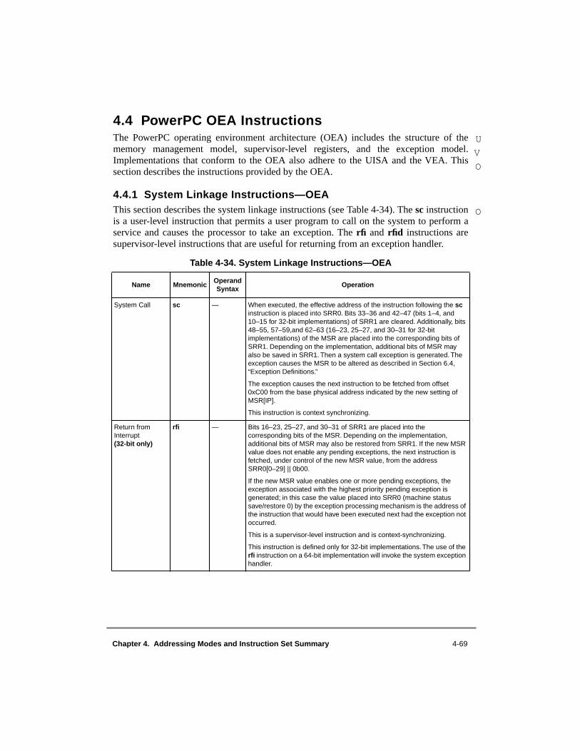
Chapter 4. Addressing Modes and Instruction Set Summary 4-69
4.4 PowerPC OEA InstructionsThe PowerPC operating environment architecture (OEA) includes the structure of thememory management model, supervisor-level registers, and the exception model.Implementations that conform to the OEA also adhere to the UISA and the VEA. Thissection describes the instructions provided by the OEA.
4.4.1 System Linkage Instructions—OEAThis section describes the system linkage instructions (see Table 4-34). The sc instructionis a user-level instruction that permits a user program to call on the system to perform aservice and causes the processor to take an exception. The rfi and rfid instructions aresupervisor-level instructions that are useful for returning from an exception handler.
Table 4-34. System Linkage Instructions—OEA
Name MnemonicOperand Syntax
Operation
System Call sc — When executed, the effective address of the instruction following the sc instruction is placed into SRR0. Bits 33–36 and 42–47 (bits 1–4, and 10–15 for 32-bit implementations) of SRR1 are cleared. Additionally, bits 48–55, 57–59,and 62–63 (16–23, 25–27, and 30–31 for 32-bit implementations) of the MSR are placed into the corresponding bits of SRR1. Depending on the implementation, additional bits of MSR may also be saved in SRR1. Then a system call exception is generated. The exception causes the MSR to be altered as described in Section 6.4, “Exception Definitions.”
The exception causes the next instruction to be fetched from offset 0xC00 from the base physical address indicated by the new setting of MSR[IP].
This instruction is context synchronizing.
Return from Interrupt(32-bit only)
rfi — Bits 16–23, 25–27, and 30–31 of SRR1 are placed into the corresponding bits of the MSR. Depending on the implementation, additional bits of MSR may also be restored from SRR1. If the new MSR value does not enable any pending exceptions, the next instruction is fetched, under control of the new MSR value, from the address SRR0[0–29] || 0b00.
If the new MSR value enables one or more pending exceptions, the exception associated with the highest priority pending exception is generated; in this case the value placed into SRR0 (machine status save/restore 0) by the exception processing mechanism is the address of the instruction that would have been executed next had the exception not occurred.
This is a supervisor-level instruction and is context-synchronizing.
This instruction is defined only for 32-bit implementations. The use of the rfi instruction on a 64-bit implementation will invoke the system exception handler.
U
V
O
O

4-70 PowerPC Microprocessor Family: The Programming Environments, Rev. 1
4.4.2 Processor Control Instructions—OEAThis section describes the processor control instructions that are used to read from andwrite to the MSR and the SPRs.
64-BIT BRIDGE
Return from Interrupt rfi — Bits 0, 48–55, 57–59, and 62–63 of SRR1 are placed into the
corresponding bits of the MSR. Depending on the implementation, additional bits of MSR may also be restored from SRR1. If the new MSR value does not enable any pending exceptions, the next instruction is fetched, under control of the new MSR value, from the address SRR0 [0–61] || 0b00 (when SF = 1 in the new MSR value) or 0x0000_0000 || SRR0[32–61] || 0b00 (when SF = 0 in the new MSR value).
If the new MSR value enables one or more pending exceptions, the exception associated with the highest priority pending exception is generated; in this case, the value placed into SRR0 (machine status save/restore 0) by the exception processing mechanism is the address of the instruction that would have been executed next had the exception not occurred.
This is a supervisor-level instruction and is context-synchronizing.
Return from Interrupt Double Word(64-bit only)
rfid — Bits 0, 48–55, 57–59, and 62–63 of SRR1 are placed into the corresponding bits of the MSR. Depending on the implementation, additional bits of MSR may also be restored from SRR1. If the new MSR value does not enable any pending exceptions, the next instruction is fetched, under control of the new MSR value, from the address SRR0[0–61] || 0b00 (default 64-bit mode) or (32)0 || the low-order 32 bits of SRR0 || 0b00 (32-bit mode of 64-bit implementations).
If the new MSR value enables one or more pending exceptions, the exception associated with the highest priority pending exception is generated; in this case, the value placed into SRR0 (machine status save/restore 0) by the exception processing mechanism is the address of the instruction that would have been executed next had the exception not occurred.
This is a supervisor-level instruction and is context-synchronizing.
This instruction is defined only for 64-bit implementations. The use of the rfid instruction on a 32-bit implementation will invoke the system exception handler.
Table 4-34. System Linkage Instructions—OEA (Continued)
Name MnemonicOperand Syntax
Operation

Chapter 4. Addressing Modes and Instruction Set Summary 4-71
4.4.2.1 Move to/from Machine State Register InstructionsTable 4-35 summarizes the instructions used for reading from and writing to the MSR.
4.4.2.2 Move to/from Special-Purpose Register Instructions (OEA)Provided is a brief description of the mtspr and mfspr instructions (see Table 4-36). Formore detailed information, see Chapter 8, “Instruction Set.” Simplified mnemonics areprovided for the mtspr and mfspr instructions in Appendix F, “Simplified Mnemonics.”For a discussion of context synchronization requirements when altering certain SPRs, referto Appendix E, “Synchronization Programming Examples.”
Table 4-35. Move to/from Machine State Register Instructions
Name MnemonicOperand Syntax
Operation
Move to Machine State Register(32-bit only)
mtmsr rS The contents of rS are placed into the MSR.
This instruction is a supervisor-level instruction and is context synchronizing except with respect to alterations to the POW and LE bits. Refer to Section 2.3.18, “Synchronization Requirements for Special Registers and for Lookaside Buffers,” for more information.
64-BIT BRIDGE
Move to Machine State Register mtmsr rS Bits 32–63 of rS are placed into the MSR. Bits 0–31 of the MSR
remain unchanged.
This instruction is a supervisor-level instruction and is context synchronizing except with respect to alterations to the POW and LE bits. Refer to Section 2.3.18, “Synchronization Requirements for Special Registers and for Lookaside Buffers,” for more information.
Move to Machine State Register Double Word(64-bit only)
mtmsrd rS The contents of rS are placed into the MSR.
This instruction is a supervisor-level instruction and is context synchronizing except with respect to alterations to the POW and LE bits. Refer to Section 2.3.18, “Synchronization Requirements for Special Registers and for Lookaside Buffers,” for more information.
Move from Machine State Register
mfmsr rD The contents of the MSR are placed into rD. This is a supervisor-level instruction.
Table 4-36. Move to/from Special-Purpose Register Instructions (OEA)
Name MnemonicOperand Syntax
Operation
Move to Special- Purpose Register
mtspr SPR,rS The SPR field denotes a special-purpose register. The contents of rS are placed into the designated SPR. For SPRs that are 32 bits long, the contents of the low-order 32 bits of rS are placed into the SPR.
For this instruction, SPRs TBL and TBU are treated as separate 32-bit registers; setting one leaves the other unaltered.
Move from Special- Purpose Register
mfspr rD,SPR The SPR field denotes a special-purpose register. The contents of the designated SPR are placed into rD.

4-72 PowerPC Microprocessor Family: The Programming Environments, Rev. 1
For mtspr and mfspr instructions, the SPR number coded in assembly language does notappear directly as a 10-bit binary number in the instruction. The number coded is split intotwo 5-bit halves that are reversed in the instruction encoding, with the high-order 5 bitsappearing in bits 16–20 of the instruction encoding and the low-order 5 bits in bits 11–15.
For information on SPR encodings (both user- and supervisor-level), see Chapter 8,“Instruction Set.” Note that there are additional SPRs specific to each implementation; forimplementation-specific SPRs, see the user’s manual for that particular processor.
4.4.3 Memory Control Instructions—OEAMemory control instructions include the following types of instructions:
• Cache management instructions (supervisor-level and user-level)• Segment register manipulation instructions• Translation lookaside buffer management instructions
This section describes supervisor-level memory control instructions. See Section 4.3.3,“Memory Control Instructions—VEA,” for more information about user-level cachemanagement instructions.
4.4.3.1 Supervisor-Level Cache Management InstructionTable 4-37 summarizes the operation of the only supervisor-level cache managementinstruction. See Section 4.3.3.1, “User-Level Cache Instructions—VEA,” for cacheinstructions that provide user-level programs the ability to manage the on-chip caches.
Note that any cache control instruction that generates an effective address that correspondsto a direct-store segment (segment descriptor[T] = 1) is treated as a no-op. However, notethat the direct-store facility is being phased out of the architecture and will not likely besupported in future devices.

Chapter 4. Addressing Modes and Instruction Set Summary 4-73
4.4.3.2 Segment Register Manipulation InstructionsThe instructions listed in Table 4-38 provide access to the segment registers for 32-bitimplementations, and effective segments 0 through 15 through the use of the optional 64-bit bridge instructions. These instructions operate completely independently of theMSR[IR] and MSR[DR] bit settings. Refer to Section 2.3.18, “SynchronizationRequirements for Special Registers and for Lookaside Buffers,” for serializationrequirements and other recommended precautions to observe when manipulating thesegment registers.
Table 4-37. Cache Management Supervisor-Level Instruction
Name MnemonicOperand Syntax
Operation
Data Cache Block Invalidate
dcbi rA,rB The EA is the sum (rA|0) + (rB).
The action taken depends on the memory mode associated with the target, and the state (modified, unmodified) of the cache block. The following list describes the action to take if the cache block containing the byte addressed by the EA is or is not in the cache.
• Coherency required (WIM = xx1)— Unmodified cache block—Invalidates copies of the cache block in the
caches of all processors.— Modified cache block—Invalidates copies of the cache block in the caches
of all processors. (Discards the modified contents.)— Absent cache block—If copies are in the caches of any other processor,
causes the copies to be invalidated. (Discards any modified contents.)• Coherency not required (WIM = xx0)
— Unmodified cache block—Invalidates the cache block in the local cache.— Modified cache block—Invalidates the cache block in the local cache.
(Discards the modified contents.)— Absent cache block—No action is taken.
When data address translation is enabled, MSR[DT]=1, and the logical (effective) address has no translation, a data access exception occurs.
The function of this instruction is independent of the write-through and cache-inhibited/allowed modes determined by the WIM bit settings of the block containing the byte addressed by the EA.
This instruction is treated as a store to the addressed byte with respect to address translation and protection, except that the change bit need not be set, and if the change bit is not set then the reference bit need not be set.

4-74 PowerPC Microprocessor Family: The Programming Environments, Rev. 1
Table 4-38. Segment Register Manipulation Instructions
Name MnemonicOperand Syntax
Operation
Move to Segment Register(32-bit only)
mtsr SR,rS The contents of rS are placed into segment register specified by operand SR.
This is a supervisor-level instruction.
64-BIT BRIDGE
Move to Segment Register mtsr SR,rS The SLB entry selected by SR is set as though it were loaded from a
segment table entry. Refer to Section 8.2, “PowerPC Instruction Set,” for additional information about the operation of the 64-bit bridge mtsr instruction.
This instruction is a supervisor-level instruction.
64-BIT BRIDGE
Move to Segment Register Double Word
mtsrd SR,rS The SLB entry selected by SR is set as though it were loaded from a segment table entry. Refer to Section 8.2, “PowerPC Instruction Set,” for additional information about the operation of the 64-bit bridge mtsrd instruction.
This instruction is a supervisor-level instruction.
This instruction is defined only for 64-bit implementations. The use of the mtsrd instruction on a 32-bit implementation will invoke the system exception handler.
64-BIT BRIDGE
Move to Segment Register Double Word Indirect
mtsrdin rS,rB The SLB entry selected by bits 32–35 of register rB is set as though it were loaded from a segment table entry. Refer to Section 8.2, “PowerPC Instruction Set,” for additional information about the operation of the 64-bit bridge mtsrdin instruction.
This instruction is a supervisor-level instruction.
This instruction is defined only for 64-bit implementations. The use of the mtsrdin instruction on a 32-bit implementation will invoke the system exception handler.
Move to Segment Register Indirect(32-bit only)
mtsrin rS,rB The contents of rS are copied to the segment register selected by bits 0–3 of rB.
This is a supervisor-level instruction.
64-BIT BRIDGE
Move to Segment Register Indirect mtsrin rS,rB The SLB entry selected by bits 32–35 of register rB is set as though it
were loaded from a segment table entry. Refer to Section 8.2, “PowerPC Instruction Set,” for additional information about the operation of the 64-bit bridge mtsrin instruction.
This instruction is a supervisor-level instruction.
Move from Segment Register(32-bit only)
mfsr rD,SR The contents of the segment register specified by operand SR are placed into rD.
This is a supervisor-level instruction.

Chapter 4. Addressing Modes and Instruction Set Summary 4-75
4.4.3.3 Translation and Segment Lookaside Buffer Management Instructions
The address translation mechanism is defined in terms of segment descriptors and pagetable entries (PTEs) used by PowerPC processors to locate the logical-to-physical addressmapping for a particular access. These segment descriptors and PTEs reside in segmenttables and page tables in memory, respectively.
For performance reasons, many processors implement a segment lookaside buffer (SLB)(for 64-bit implementations) and one or more translation lookaside buffers on-chip. Theseare caches of portions of the segment table and page table, respectively. As changes aremade to the address translation tables, it is necessary to maintain coherency between theSLB and TLB and the updated tables. This is done by invalidating SLB and TLB entries, oroccasionally by invalidating the entire SLB or TLB, and allowing the translation cachingmechanism to refetch from the tables. Note that in 32-bit implementations, segmentdescriptors reside in 16 segment registers, and no other segment tables in memory (orSLBs) are defined.
Each PowerPC implementation that has an SLB provides means for invalidating anindividual SLB entry and invalidating the entire SLB. Each PowerPC implementation thathas a TLB provides means for invalidating an individual TLB entry and invalidating theentire TLB.
If a 64-bit implementation does not implement an SLB, it treats the correspondinginstructions (slbie and slbia) either as no-ops or as illegal instructions. Similarly, if aprocessor does not implement a TLB, it treats the corresponding instructions (tlbie, tlbia,and tlbsync) either as no-ops or as illegal instructions.
64-BIT BRIDGE
Move from Segment Register mfsr rD,SR The contents of the SLB entry specified by operand SR are placed into
rD. Refer to Section 8.2, “PowerPC Instruction Set,” for additional information about the operation of the 64-bit bridge mfsr instruction.
This instruction is a supervisor-level instruction.
Move from Segment Register Indirect(32-bit only)
mfsrin rD,rB The contents of the segment register selected by bits 0–3 of rB are copied into rD.
This is a supervisor-level instruction.
64-BIT BRIDGE
Move from Segment Register Indirect mfsrin rD,rB The contents of the SLB entry specified by bits 32–35 of rB are placed
into rD. Refer to Section 8.2, “PowerPC Instruction Set,” for additional information about the operation of the 64-bit bridge mfsrin instruction.
This instruction is a supervisor-level instruction.
Table 4-38. Segment Register Manipulation Instructions (Continued)
Name MnemonicOperand Syntax
Operation
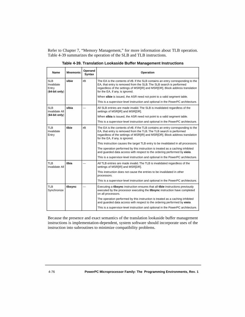
4-76 PowerPC Microprocessor Family: The Programming Environments, Rev. 1
Refer to Chapter 7, “Memory Management,” for more information about TLB operation.Table 4-39 summarizes the operation of the SLB and TLB instructions.
Because the presence and exact semantics of the translation lookaside buffer managementinstructions is implementation-dependent, system software should incorporate uses of theinstruction into subroutines to minimize compatibility problems.
Table 4-39. Translation Lookaside Buffer Management Instructions
Name MnemonicOperand Syntax
Operation
SLB Invalidate Entry(64-bit only)
slbie rB The EA is the contents of rB. If the SLB contains an entry corresponding to the EA, that entry is removed from the SLB. The SLB search is performed regardless of the settings of MSR[IR] and MSR[DR]. Block address translation for the EA, if any, is ignored.
When slbie is issued, the ASR need not point to a valid segment table.
This is a supervisor-level instruction and optional in the PowerPC architecture.
SLB Invalidate All(64-bit only)
slbia — All SLB entries are made invalid. The SLB is invalidated regardless of the settings of MSR[IR] and MSR[DR].
When slbia is issued, the ASR need not point to a valid segment table.
This is a supervisor-level instruction and optional in the PowerPC architecture.
TLB Invalidate Entry
tlbie rB The EA is the contents of rB. If the TLB contains an entry corresponding to the EA, that entry is removed from the TLB. The TLB search is performed regardless of the settings of MSR[IR] and MSR[DR]. Block address translation for the EA, if any, is ignored.
This instruction causes the target TLB entry to be invalidated in all processors.
The operation performed by this instruction is treated as a caching inhibited and guarded data access with respect to the ordering performed by eieio.
This is a supervisor-level instruction and optional in the PowerPC architecture.
TLB Invalidate All
tlbia — All TLB entries are made invalid. The TLB is invalidated regardless of the settings of MSR[IR] and MSR[DR].
This instruction does not cause the entries to be invalidated in other processors.
This is a supervisor-level instruction and optional in the PowerPC architecture.
TLB Synchronize
tlbsync — Executing a tlbsync instruction ensures that all tlbie instructions previously executed by the processor executing the tlbsync instruction have completed on all processors.
The operation performed by this instruction is treated as a caching inhibited and guarded data access with respect to the ordering performed by eieio.
This is a supervisor-level instruction and optional in the PowerPC architecture.

Chapter 5. Cache Model and Memory Coherency 5-1
Chapter 5 Cache Model and Memory Coherency 5050
This chapter summarizes the cache model as defined by the virtual environmentarchitecture (VEA) as well as the built-in architectural controls for maintaining memorycoherency. This chapter describes the cache control instructions and special concerns formemory coherency in single-processor and multiprocessor systems. Aspects of theoperating environment architecture (OEA) as they relate to the cache model and memorycoherency are also covered.
The PowerPC architecture provides for relaxed memory coherency. Features such as write-back caching and out-of-order execution allow software engineers to exploit theperformance benefits of weakly-ordered memory access. The architecture also provides themeans to control the order of accesses for order-critical operations.
In this chapter, the term multiprocessor is used in the context of maintaining cachecoherency. In this context, a system could include other devices that access system memory,maintain independent caches, and function as bus masters.
Each cache management instruction operates on an aligned unit of memory. The VEAdefines this cacheable unit as a block. Since the term ‘block’ is easily confused with the unitof memory addressed by the block address translation (BAT) mechanism, this chapter usesthe term ‘cache block’ to indicate the cacheable unit. The size of the cache block can varyby instruction and by implementation. In addition, the unit of memory at which coherencyis maintained is called the coherence block. The size of the coherence block is alsoimplementation-specific. However, the coherence block is often the same size as the cacheblock.
5.1 The Virtual EnvironmentThe user instruction set architecture (UISA) relies upon a memory space of 264 (232 in 32-bit implementations) bytes for applications. The VEA expands upon the memory model byintroducing virtual memory, caches, and shared memory multiprocessing. Although manyapplications will not need to access the features introduced by the VEA, it is important thatprogrammers are aware that they are working in a virtual environment where the physicalmemory may be shared by multiple processes running on one or more processors.
U
V
O
V

5-2 PowerPC Microprocessor Family: The Programming Environments, Rev. 1
This section describes load and store ordering, atomicity, the cache model, memorycoherency, and the VEA cache management instructions. The features of the VEA areaccessible to both user-level and supervisor-level applications (referred to as problem stateand privileged state, respectively, in the architecture specification).
The mechanism for controlling the virtual memory space is defined by the OEA. Thefeatures of the OEA are accessible to supervisor-level applications only (typically operatingsystems). For more information on the address translation mechanism, refer to Chapter 7,“Memory Management.”
5.1.1 Memory Access OrderingThe VEA specifies a weakly consistent memory model for shared memory multiprocessorsystems. This model provides an opportunity for significantly improved performance overa model that has stronger consistency rules, but places the responsibility for access orderingon the programmer. When a program requires strict access ordering for proper execution,the programmer must insert the appropriate ordering or synchronization instructions intothe program.
The order in which the processor performs memory accesses, the order in which thoseaccesses complete in memory, and the order in which those accesses are viewed asoccurring by another processor may all be different. A means of enforcing memory accessordering is provided to allow programs (or instances of programs) to share memory. Similarmeans are needed to allow programs executing on a processor to share memory with someother mechanism, such as an I/O device, that can also access memory.
Various facilities are provided that enable programs to control the order in which memoryaccesses are performed by separate instructions. First, if separate store instructions accessmemory that is designated as both caching-inhibited and guarded, the accesses areperformed in the order specified by the program. Refer to Section 5.1.4, “MemoryCoherency,” and Section 5.2.1, “Memory/Cache Access Attributes,” for a completedescription of the caching-inhibited and guarded attributes. Additionally, two instructions,eieio and sync, are provided that enable the program to control the order in which thememory accesses caused by separate instructions are performed.
No ordering should be assumed among the memory accesses caused by a single instruction(that is, by an instruction for which multiple accesses are not atomic), and no means areprovided for controlling that order. Chapter 4, “Addressing Modes and Instruction SetSummary,” contains additional information about the sync and eieio instructions.
5.1.1.1 Enforce In-Order Execution of I/O InstructionThe eieio instruction permits the program to control the order in which loads and stores areperformed when the accessed memory has certain attributes, as described in Chapter 8,“Instruction Set.” For example, eieio can be used to ensure that a sequence of load and storeoperations to an I/O device’s control registers updates those registers in the desired order.

Chapter 5. Cache Model and Memory Coherency 5-3
The eieio instruction can also be used to ensure that all stores to a shared data structure arevisible to other processors before the store that releases the lock is visible to them.
The eieio instruction may complete before memory accesses caused by instructionspreceding the eieio instruction have been performed with respect to system memory orcoherent storage as appropriate.
If stronger ordering is desired, the sync instruction must be used.
5.1.1.2 Synchronize InstructionWhen a portion of memory that requires coherency must be forced to a known state, it isnecessary to synchronize memory with respect to other processors and mechanisms. Thissynchronization is accomplished by requiring programs to indicate explicitly in theinstruction stream, by inserting a sync instruction, that synchronization is required. Onlywhen sync completes are the effects of all coherent memory accesses previously executedby the program guaranteed to have been performed with respect to all other processors andmechanisms that access those locations coherently.
The sync instruction ensures that all the coherent memory accesses, initiated by a program,have been performed with respect to all other processors and mechanisms that access thetarget locations coherently, before its next instruction is executed. A program can use thisinstruction to ensure that all updates to a shared data structure, accessed coherently, arevisible to all other processors that access the data structure coherently, before executing astore that will release a lock on that data structure. Execution of the sync instruction doesthe following:
• Performs the functions described for the sync instruction in Section 4.2.6, “Memory Synchronization Instructions—UISA.”
• Ensures that consistency operations, and the effects of icbi, dcbz, dcbst, dcbf, dcba, and dcbi instructions previously executed by the processor executing sync, have completed on such other processors as the memory/cache access attributes of the target locations require.
• Ensures that TLB invalidate operations previously executed by the processor executing the sync have completed on that processor. The sync instruction does not wait for such invalidates to complete on other processors.
• Ensures that memory accesses due to instructions previously executed by the processor executing the sync are recorded in the R and C bits in the page table and that the new values of those bits are visible to all processors and mechanisms; refer to Section 7.5.3, “Page History Recording.”
The sync instruction is execution synchronizing. It is not context synchronizing, andtherefore need not discard prefetched instructions.
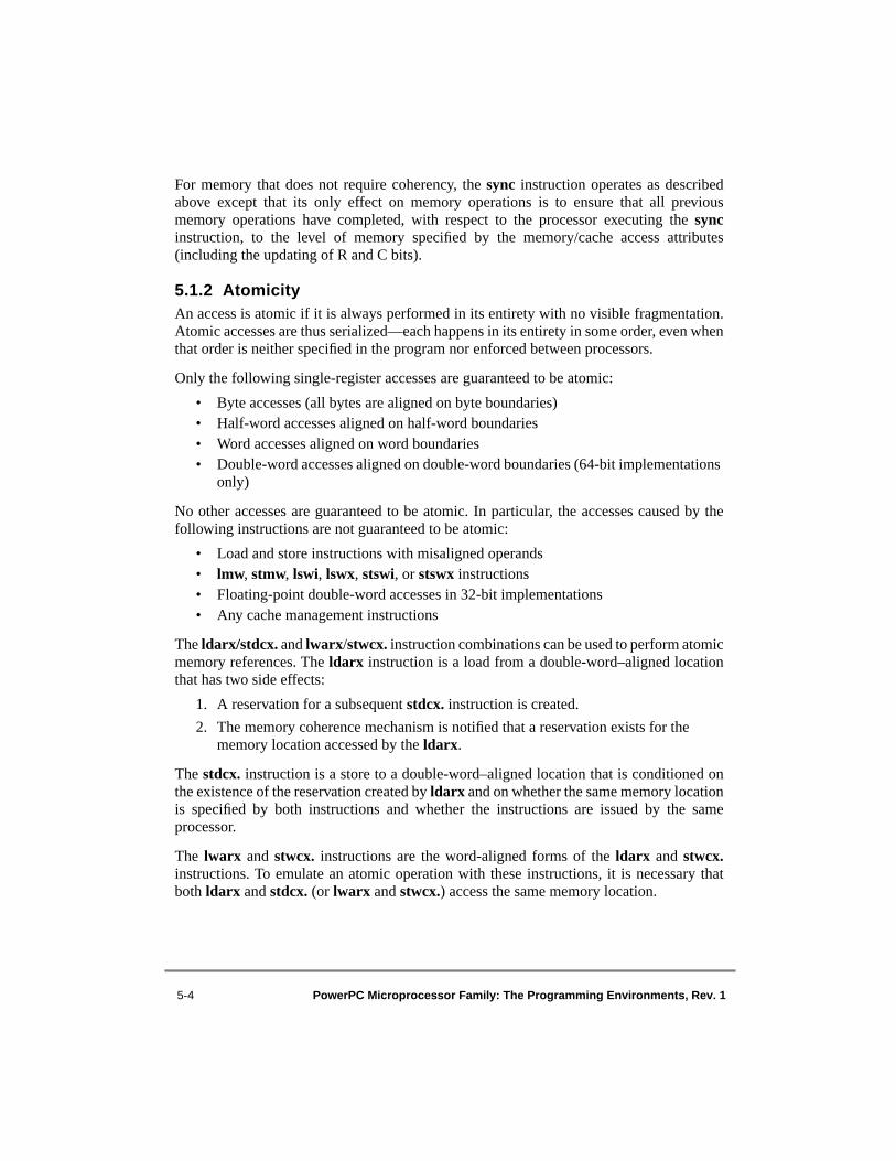
5-4 PowerPC Microprocessor Family: The Programming Environments, Rev. 1
For memory that does not require coherency, the sync instruction operates as describedabove except that its only effect on memory operations is to ensure that all previousmemory operations have completed, with respect to the processor executing the syncinstruction, to the level of memory specified by the memory/cache access attributes(including the updating of R and C bits).
5.1.2 AtomicityAn access is atomic if it is always performed in its entirety with no visible fragmentation.Atomic accesses are thus serialized—each happens in its entirety in some order, even whenthat order is neither specified in the program nor enforced between processors.
Only the following single-register accesses are guaranteed to be atomic:
• Byte accesses (all bytes are aligned on byte boundaries)• Half-word accesses aligned on half-word boundaries• Word accesses aligned on word boundaries• Double-word accesses aligned on double-word boundaries (64-bit implementations
only)
No other accesses are guaranteed to be atomic. In particular, the accesses caused by thefollowing instructions are not guaranteed to be atomic:
• Load and store instructions with misaligned operands• lmw, stmw, lswi, lswx, stswi, or stswx instructions• Floating-point double-word accesses in 32-bit implementations• Any cache management instructions
The ldarx/stdcx. and lwarx/stwcx. instruction combinations can be used to perform atomicmemory references. The ldarx instruction is a load from a double-word–aligned locationthat has two side effects:
1. A reservation for a subsequent stdcx. instruction is created.
2. The memory coherence mechanism is notified that a reservation exists for the memory location accessed by the ldarx.
The stdcx. instruction is a store to a double-word–aligned location that is conditioned onthe existence of the reservation created by ldarx and on whether the same memory locationis specified by both instructions and whether the instructions are issued by the sameprocessor.
The lwarx and stwcx. instructions are the word-aligned forms of the ldarx and stwcx.instructions. To emulate an atomic operation with these instructions, it is necessary thatboth ldarx and stdcx. (or lwarx and stwcx.) access the same memory location.
Chapter 5. Cache Model and Memory Coherency 5-5
In a multiprocessor system, every processor (other than the one executing ldarx/stdcx. orlwarx/stwcx.) that might update the location must configure the addressed page as memorycoherency required. The ldarx/stdcx. and lwarx/stwcx. instructions function in caching-inhibited, as well as in caching-allowed, memory. If the addressed memory is in write-through mode, it is implementation-dependent whether these instructions functioncorrectly or cause the DSI exception handler to be invoked. (Note that exceptions arereferred to as interrupts in the architecture specification.)
The ldarx/stdcx. and lwarx/stwcx. instruction combinations are described inSection 4.2.6, “Memory Synchronization Instructions—UISA,” and Chapter 8,“Instruction Set.”
5.1.3 Cache ModelThe PowerPC architecture does not specify the type, organization, implementation, or eventhe existence of a cache. The standard cache model has separate instruction and data caches,also known as a Harvard cache model. However, the architecture allows for many differentcache types. Some implementations will have a unified cache (where there is a single cachefor both instructions and data). Other implementations may not have a cache at all.
The function of the cache management instructions depends on the implementation of thecache(s) and the setting of the memory/cache access modes. For a program to executeproperly on all implementations, software should use the Harvard model. In cases where aprocessor is implemented without a cache, the architecture guarantees that instructionsaffecting the nonimplemented cache will not halt execution (note that dcbz may cause analignment exception on some implementations). For example, a processor with no cachemay treat a cache instruction as a no-op. Or, a processor with a unified cache may treat theicbi instruction as a no-op. In this manner, programs written for separate instruction anddata caches will run on all compliant implementations.
5.1.4 Memory Coherency The primary objective of a coherent memory system is to provide the same image ofmemory to all devices using the system. The VEA and OEA define coherency controls thatfacilitate synchronization, cooperative use of shared resources, and task migration amongprocessors. These controls include the memory/cache access attributes, the sync and eieioinstructions, and the ldarx/stdcx. and lwarx/stwcx. instruction pairs. Without thesecontrols, the processor could not support a weakly-ordered memory access model.
A strongly-ordered memory access model hinders performance by requiring excessiveoverhead, particularly in multiprocessor environments. For example, a processorperforming a store operation in a strongly-ordered system requires exclusive access to anaddress before making an update, to prevent another device from using stale data.
The VEA defines a page as a unit of memory for which protection and control attributes areindependently specifiable. The OEA (supervisor level) specifies the size of a page as4 Kbytes. It is important to note that the VEA (user level) does not specify the page size.

5-6 PowerPC Microprocessor Family: The Programming Environments, Rev. 1
5.1.4.1 Memory/Cache Access ModesThe OEA defines the set of memory/cache access modes and the mechanism to implementthese modes. Refer to Section 5.2.1, “Memory/Cache Access Attributes,” for moreinformation. However, the VEA specifies that at the user level, the operating system can beexpected to provide the following attributes for each page of memory:
• Write-through or write-back• Caching-inhibited or caching-allowed• Memory coherency required or memory coherency not required• Guarded or not guarded
User-level programs specify the memory/cache access attributes through an operatingsystem service.
5.1.4.1.1 Pages Designated as Write-ThroughWhen a page is designated as write-through, store operations update the data in the cacheand also update the data in main memory. The processor writes to the cache and through tomain memory. Load operations use the data in the cache, if it is present.
In write-back mode, the processor is only required to update data in the cache. Theprocessor may (but is not required to) update main memory. Load and store operations usethe data in the cache, if it is present. The data in main memory does not necessarily stayconsistent with that same location’s data in the cache. Many implementations automaticallyupdate main memory in response to a memory access by another device (for example, asnoop hit). In addition, the dcbst and dcbf instructions can be used to explicitly force anupdate of main memory.
The write-through attribute is meaningless for locations designated as caching-inhibited.
5.1.4.1.2 Pages Designated as Caching-InhibitedWhen a page is designated as caching-inhibited, the processor bypasses the cache andperforms load and store operations to main memory. When a page is designated as caching-allowed, the processor uses the cache and performs load and store operations to the cacheor main memory depending on the other memory/cache access attributes for the page.
It is important that all locations in a page are purged from the cache prior to changing thememory/cache access attribute for the page from caching-allowed to caching-inhibited. Itis considered a programming error if a caching-inhibited memory location is found in thecache. Software must ensure that the location has not previously been brought into thecache, or, if it has, that it has been flushed from the cache. If the programming error occurs,the result of the access is boundedly undefined.

Chapter 5. Cache Model and Memory Coherency 5-7
5.1.4.1.3 Pages Designated as Memory Coherency RequiredWhen a page is designated as memory coherency required, store operations to that locationare serialized with all stores to that same location by all other processors that also accessthe location coherently.This can be implemented, for example, by an ownership protocolthat allows at most one processor at a time to store to the location. Moreover, the currentcopy of a cache block that is in this mode may be copied to main storage any number oftimes, for example, by successive dcbst instructions.
Coherency does not ensure that the result of a store by one processor is visible immediatelyto all other processors and mechanisms. Only after a program has executed the syncinstruction are the previous storage accesses it executed guaranteed to have been performedwith respect to all other processors and mechanisms.
5.1.4.1.4 Pages Designated as Memory Coherency Not RequiredFor a memory area that is configured such that coherency is not required, software mustensure that the data cache is consistent with main storage before changing the mode orallowing another device to access the area.
Executing a dcbst or dcbf instruction specifying a cache block that is in this mode causesthe block to be copied to main memory if and only if the processor modified the contentsof a location in the block and the modified contents have not been written to main memory.
In a single-cache system, correct coherent execution may likely not require memorycoherency; therefore, using memory coherency not required mode improves performance.
5.1.4.1.5 Pages Designated as GuardedThe guarded attribute pertains to out-of-order execution. Refer to Section 5.2.1.5.3, “Out-of-Order Accesses to Guarded Memory,” for more information about out-of-orderexecution.
When a page is designated as guarded, instructions and data cannot be accessed out oforder. Additionally, if separate store instructions access memory that is both caching-inhibited and guarded, the accesses are performed in the order specified by the program.When a page is designated as not guarded, out-of-order fetches and accesses are allowed.
5.1.4.2 Coherency PrecautionsMismatched memory/cache attributes cause coherency paradoxes in both single-processorand multiprocessor systems. When the memory/cache access attributes are changed, it iscritical that the cache contents reflect the new attribute settings. For example, if a block orpage that had allowed caching becomes caching-inhibited, the appropriate cache blocksshould be flushed to leave no indication that caching had previously been allowed.
Although coherency paradoxes are considered programming errors, specificimplementations may attempt to handle the offending conditions and minimize the negativeeffects on memory coherency. Bus operations that are generated for specific instructionsand state conditions are not defined by the architecture.

5-8 PowerPC Microprocessor Family: The Programming Environments, Rev. 1
5.1.5 VEA Cache Management InstructionsThe VEA defines instructions for controlling both the instruction and data caches. Forimplementations that have a unified instruction/data cache, instruction cache controlinstructions are valid instructions, but may function differently.
Note that any cache control instruction that generates an EA that corresponds to a direct-store segment (SR[T] = 1 or STE[T] = 1) is treated as a no-op. However, the direct-storefacility is being phased out of the architecture and will not likely be supported in futuredevices. Thus, software should not depend on its effects.
This section briefly describes the cache management instructions available to programs atthe user privilege level. Additional descriptions of coding the VEA cache managementinstructions is provided in Chapter 4, “Addressing Modes and Instruction Set Summary,”and Chapter 8, “Instruction Set.” In the following instruction descriptions, the target is thecache block containing the byte addressed by the effective address.
5.1.5.1 Data Cache InstructionsData caches and unified caches must be consistent with other caches (data or unified),memory, and I/O data transfers. To ensure consistency, aliased effective addresses (twoeffective addresses that map to the same physical address) must have the same page offset.Note that physical address is referred to as real address in the architecture specification.
5.1.5.1.1 Data Cache Block Touch (dcbt) and Data Cache Block Touch for Store (dcbtst) Instructions
These instructions provide a method for improving performance through the use ofsoftware-initiated prefetch hints. However, these instructions do not guarantee that a cacheblock will be fetched.
A program uses the dcbt instruction to request a cache block fetch before it is needed bythe program. The program can then use the data from the cache rather than fetching frommain memory.
The dcbtst instruction behaves similarly to the dcbt instruction. A program uses dcbtst torequest a cache block fetch to guarantee that a subsequent store will be to a cached location.
The processor does not invoke the exception handler for translation or protection violationscaused by either of the touch instructions. Additionally, memory accesses caused by theseinstructions are not necessarily recorded in the page tables. If an access is recorded, then itis treated in a manner similar to that of a load from the addressed byte. Someimplementations may not take any action based on the execution of these instructions, orthey may prefetch the cache block corresponding to the EA into their cache. Forinformation about the R and C bits, see Section 7.5.3, “Page History Recording.”

Chapter 5. Cache Model and Memory Coherency 5-9
Both dcbt and dcbtst are provided for performance optimization. These instructions do notaffect the correct execution of a program, regardless of whether they succeed (fetch thecache block) or fail (do not fetch the cache block). If the target block is not accessible tothe program for loads, then no operation occurs.
5.1.5.1.2 Data Cache Block Set to Zero (dcbz) InstructionThe dcbz instruction clears a single cache block as follows:
• If the target is in the data cache, all bytes of the cache block are cleared.
• If the target is not in the data cache and the corresponding page is caching-allowed, the cache block is established in the data cache (without fetching the cache block from main memory), and all bytes of the cache block are cleared.
• If the target is designated as either caching-inhibited or write-through, then either all bytes in main memory that correspond to the addressed cache block are cleared, or the alignment exception handler is invoked. The exception handler should clear all the bytes in main memory that correspond to the addressed cache block.
• If the target is designated as coherency required, and the cache block exists in the data cache(s) of any other processor(s), it is kept coherent in those caches.
The dcbz instruction is treated as a store to the addressed byte with respect to addresstranslation, protection, referenced and changed recording, and the ordering enforced byeieio or by the combination of caching-inhibited and guarded attributes for a page.
Refer to Chapter 6, “Exceptions,” for more information about a possible delayed machinecheck exception that can occur by using dcbz when the operating system has set up anincorrect memory mapping.
5.1.5.1.3 Data Cache Block Store (dcbst) InstructionThe dcbst instruction permits the program to ensure that the latest version of the targetcache block is in main memory. The dcbst instruction executes as follows:
• Coherency required—If the target exists in the data cache(s) of any processor(s) and has been modified, the data is written to main memory.
• Coherency not required—If the target exists in the data cache of the executing processor and has been modified, the data is written to main memory.
The function of this instruction is independent of the write-through/write-back andcaching-inhibited/caching-allowed attributes of the target.
The memory access caused by a dcbst instruction is not necessarily recorded in the pagetables. If the access is recorded, then it is treated as a load operation (not as a storeoperation).

5-10 PowerPC Microprocessor Family: The Programming Environments, Rev. 1
5.1.5.1.4 Data Cache Block Flush (dcbf) InstructionThe action taken depends on the memory/cache access mode associated with the target, andon the state of the cache block. The following list describes the action taken for the variouscases:
• Coherency required
Unmodified cache block—Invalidates copies of the cache block in the data caches of all processors.
Modified cache block—Copies the cache block to memory. Invalidates copies of the cache block in the data caches of all processors.
Target block not in cache—If a modified copy of the cache block is in the data cache(s) of any processor(s), dcbf causes the modified cache block to be copied to memory and then invalidated. If unmodified copies are in the data caches of other processors, dcbf causes those copies to be invalidated.
• Coherency not required
Unmodified cache block—Invalidates the cache block in the executing processor's data cache.
Modified cache block—Copies the data cache block to memory and then invalidates the cache block in the executing processor.
Target block not in cache—No action is taken.
The function of this instruction is independent of the write-through/write-back andcaching-inhibited/caching-allowed attributes of the target.
The memory access caused by a dcbf instruction is not necessarily recorded in the pagetables. If the access is recorded, then it is treated as a load operation (not as a storeoperation).
5.1.5.2 Instruction Cache InstructionsInstruction caches, if they exist, are not required to be consistent with data caches, memory,or I/O data transfers. Software must use the appropriate cache management instructions toensure that instruction caches are kept coherent when instructions are modified by theprocessor or by input data transfer. When a processor alters a memory location that may becontained in an instruction cache, software must ensure that updates to memory are visibleto the instruction fetching mechanism. Although the instructions to enforce consistencyvary among implementations, the following sequence for a uniprocessor system is typical:
1. dcbst (update memory)2. sync (wait for update)3. icbi (invalidate copy in instruction cache)4. isync (perform context synchronization)

Chapter 5. Cache Model and Memory Coherency 5-11
Note that most operating systems will provide a system service for this function. Theseoperations are necessary because the memory may be designated as write-back. Sinceinstruction fetching may bypass the data cache, changes made to items in the data cachemay not otherwise be reflected in memory until after the instruction fetch completes.
For implementations used in multiprocessor systems, variations on this sequence may berecommended. For example, in a multiprocessor system with a unified instruction/datacache (at any level), if instructions are fetched without coherency being enforced, thepreceding instruction sequence is inadequate. Because the icbi instruction does notinvalidate blocks in a unified cache, a dcbf instruction should be used instead of a dcbstinstruction for this case.
5.1.5.2.1 Instruction Cache Block Invalidate Instruction (icbi)The icbi instruction executes as follows:
• Coherency required
If the target is in the instruction cache of any processor, the cache block is made invalid in all such processors, so that the next reference causes the cache block to be refetched.
• Coherency not required
If the target is in the instruction cache of the executing processor, the cache block is made invalid in the executing processor so that the next reference causes the cache block to be refetched.
The icbi instruction is provided for use in processors with separate instruction and datacaches. The effective address is computed, translated, and checked for protection violationsas defined in Chapter 7, “Memory Management.” If the target block is not accessible to theprogram for loads, then a DSI exception occurs.
The function of this instruction is independent of the write-through/write-back andcaching-inhibited/caching-allowed attributes of the target.
The memory access caused by an icbi instruction is not necessarily recorded in the pagetables. If the access is recorded, then it is treated as a load operation. Implementations thathave a unified cache treat the icbi instruction as a no-op except that they may invalidate thetarget cache block in the instruction caches of other processors (in coherency requiredmode).
5.1.5.2.2 Instruction Synchronize Instruction (isync)The isync instruction provides an ordering function for the effects of all instructionsexecuted by a processor. Executing an isync instruction ensures that all instructionspreceding the isync instruction have completed before the isync instruction completes,except that memory accesses caused by those instructions need not have been performedwith respect to other processors and mechanisms. It also ensures that no subsequentinstructions are initiated by the processor until after the isync instruction completes.

5-12 PowerPC Microprocessor Family: The Programming Environments, Rev. 1
Finally, it causes the processor to discard any prefetched instructions, with the effect thatsubsequent instructions will be fetched and executed in the context established by theinstructions preceding the isync instruction. The isync instruction has no effect on otherprocessors or on their caches.
5.2 The Operating EnvironmentThe OEA defines the mechanism for controlling the memory/cache access modesintroduced in Section 5.1.4.1, “Memory/Cache Access Modes.” This section describes thecache-related aspects of the OEA including the memory/cache access attributes, out-of-order execution, direct-store interface considerations, and the dcbi instruction. The featuresof the OEA are accessible to supervisor-level applications only. The mechanism forcontrolling the virtual memory space is described in Chapter 7, “Memory Management.”
The memory model of PowerPC processors provides the following features:
• Flexibility to allow performance benefits of weakly-ordered memory access
• A mechanism to maintain memory coherency among processors and between a processor and I/O devices controlled at the block and page level
• Instructions that can be used to ensure a consistent memory state
• Guaranteed processor access order
The memory implementations in PowerPC systems can take advantage of the performancebenefits of weak ordering of memory accesses between processors or between processorsand other external devices without any additional complications. Memory coherency canbe enforced externally by a snooping bus design, a centralized cache directory design, orother designs that can take advantage of the coherency features of PowerPC processors.
Memory accesses performed by a single processor appear to complete sequentially fromthe view of the programming model but may complete out of order with respect to theultimate destination in the memory hierarchy. Order is guaranteed at each level of thememory hierarchy for accesses to the same address from the same processor. The dcbst,dcbf, icbi, isync, sync, eieio, ldarx, stdcx., lwarx, and stwcx. instructions allow theprogrammer to ensure a consistent memory state.
5.2.1 Memory/Cache Access AttributesAll instruction and data accesses are performed under the control of the four memory/cacheaccess attributes:
• Write-through (W attribute)• Caching-inhibited (I attribute)• Memory coherency (M attribute)• Guarded (G attribute)
O
Chapter 5. Cache Model and Memory Coherency 5-13
These attributes are programmed in the PTEs and BATs by the operating system for eachpage and block respectively. The W and I attributes control how the processor performingan access uses its own cache. The M attribute ensures that coherency is maintained for allcopies of the addressed memory location. When an access requires coherency, the processorperforming the access must inform the coherency mechanisms throughout the system thatthe access requires memory coherency. The G attribute prevents out-of-order loading andprefetching from the addressed memory location.
Note that the memory/cache access attributes are relevant only when an effective address istranslated by the processor performing the access. Note also that not all combinations ofsettings of these bits is supported. The attributes are not saved along with data in the cache(for cacheable accesses), nor are they associated with subsequent accesses made by otherprocessors.
The operating system programs the memory/cache access attribute for each page or blockas required. The WIMG attributes occupy four bits in the BAT registers for block addresstranslation and in the PTEs for page address translation. The WIMG bits are programmedas follows:
• The operating system uses the mtspr instruction to program the WIMG bits in the BAT registers for block address translation. The IBAT register pairs implement the W or G bits; however, attempting to set either bit in IBAT registers causes boundedly-undefined results.
• The operating system writes the WIMG bits for each page into the PTEs in system memory as it sets up the page tables.
Note that for data accesses performed in real addressing mode (MSR[DR] = 0), the WIMGbits are assumed to be 0b0011 (the data is write-back, caching is enabled, memorycoherency is enforced, and memory is guarded). For instruction accesses performed in realaddressing mode (MSR[IR] = 0), the WIMG bits are assumed to be 0b0001 (the data iswrite-back, caching is enabled, memory coherency is not enforced, and memory isguarded).
5.2.1.1 Write-Through Attribute (W)When an access is designated as write-through (W = 1), if the data is in the cache, a storeoperation updates the cached copy of the data. In addition, the update is written to thememory location. The definition of the memory location to be written to (in addition to thecache) depends on the implementation of the memory system but can be illustrated by thefollowing examples:
• RAM—The store is sent to the RAM controller to be written into the target RAM.
• I/O device—The store is sent to the memory-mapped I/O controller to be written to the target register or memory location.
In systems with multilevel caching, the store must be written to at least a depth in thememory hierarchy that is seen by all processors and devices.
5-14 PowerPC Microprocessor Family: The Programming Environments, Rev. 1
Multiple store instructions may be combined for write-through accesses except when thestore instructions are separated by a sync or eieio instruction. A store operation to a memorylocation designated as write-through may cause any part of the cache block to be writtenback to main memory.
Accesses that correspond to W = 0 are considered write-back. For this case, although thestore operation is performed to the cache, the data is copied to memory only when a copy-back operation is required. Use of the write-back mode (W = 0) can improve overallperformance for areas of the memory space that are seldom referenced by other processorsor devices in the system.
Accesses to the same memory location using two effective addresses for which the W bitsetting differs meet the memory-coherency requirements if the accesses are performed bya single processor. If the accesses are performed by two or more processors, coherence isenforced by the hardware only if the write-through attribute is the same for all the accesses.
5.2.1.2 Caching-Inhibited Attribute (I)If I = 1, the memory access is completed by referencing the location in main memory,bypassing the cache. During the access, the addressed location is not loaded into the cachenor is the location allocated in the cache.
It is considered a programming error if a copy of the target location of an access to caching-inhibited memory is resident in the cache. Software must ensure that the location has notbeen previously loaded into the cache, or, if it has, that it has been flushed from the cache.
Data accesses from more than one instruction may be combined for cache-inhibitedoperations, except when the accesses are separated by a sync instruction, or by an eieioinstruction when the page or block is also designated as guarded.
Instruction fetches, dcbz instructions, and load and store operations to the same memorylocation using two effective addresses for which the I bit setting differs must meet therequirement that a copy of the target location of an access to caching-inhibited memory notbe in the cache. Violation of this requirement is considered a programming error; softwaremust ensure that the location has not previously been brought into the cache or, if it has,that it has been flushed from the cache. If the programming error occurs, the result of theaccess is boundedly undefined. It is not considered a programming error if the targetlocation of any other cache management instruction to caching-inhibited memory is in thecache.
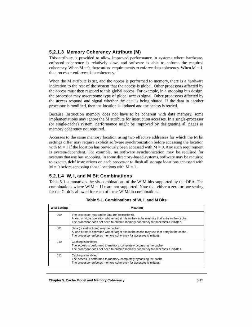
Chapter 5. Cache Model and Memory Coherency 5-15
5.2.1.3 Memory Coherency Attribute (M)This attribute is provided to allow improved performance in systems where hardware-enforced coherency is relatively slow, and software is able to enforce the requiredcoherency. When M = 0, there are no requirements to enforce data coherency. When M = 1,the processor enforces data coherency.
When the M attribute is set, and the access is performed to memory, there is a hardwareindication to the rest of the system that the access is global. Other processors affected bythe access must then respond to this global access. For example, in a snooping bus design,the processor may assert some type of global access signal. Other processors affected bythe access respond and signal whether the data is being shared. If the data in anotherprocessor is modified, then the location is updated and the access is retried.
Because instruction memory does not have to be coherent with data memory, someimplementations may ignore the M attribute for instruction accesses. In a single-processor(or single-cache) system, performance might be improved by designating all pages asmemory coherency not required.
Accesses to the same memory location using two effective addresses for which the M bitsettings differ may require explicit software synchronization before accessing the locationwith M = 1 if the location has previously been accessed with M = 0. Any such requirementis system-dependent. For example, no software synchronization may be required forsystems that use bus snooping. In some directory-based systems, software may be requiredto execute dcbf instructions on each processor to flush all storage locations accessed withM = 0 before accessing those locations with M = 1.
5.2.1.4 W, I, and M Bit CombinationsTable 5-1 summarizes the six combinations of the WIM bits supported by the OEA. Thecombinations where WIM = 11x are not supported. Note that either a zero or one settingfor the G bit is allowed for each of these WIM bit combinations.
Table 5-1. Combinations of W, I, and M Bits
WIM Setting Meaning
000 The processor may cache data (or instructions). A load or store operation whose target hits in the cache may use that entry in the cache. The processor does not need to enforce memory coherency for accesses it initiates.
001 Data (or instructions) may be cached. A load or store operation whose target hits in the cache may use that entry in the cache. The processor enforces memory coherency for accesses it initiates.
010 Caching is inhibited. The access is performed to memory, completely bypassing the cache. The processor does not need to enforce memory coherency for accesses it initiates.
011 Caching is inhibited. The access is performed to memory, completely bypassing the cache. The processor enforces memory coherency for accesses it initiates.

5-16 PowerPC Microprocessor Family: The Programming Environments, Rev. 1
5.2.1.5 The Guarded Attribute (G)When the guarded bit is set, the memory area (block or page) is designated as guarded. Thissetting can be used to protect certain memory areas from read accesses made by theprocessor that are not dictated directly by the program. If there are areas of physicalmemory that are not fully populated (in other words, there are holes in the physical memorymap within this area), this setting can protect the system from undesired accesses causedby out-of-order load operations or instruction prefetches that could lead to the generationof the machine check exception. Also, the guarded bit can be used to prevent out-of-order(speculative) load operations or prefetches from occurring to certain peripheral devices thatproduce undesired results when accessed in this way.
5.2.1.5.1 Performing Operations Out of OrderAn operation is said to be performed in-order if it is guaranteed to be required by thesequential execution model. Any other operation is said to be performed out of order.
Operations are performed out of order by the hardware on the expectation that the resultswill be needed by an instruction that will be required by the sequential execution model.Whether the results are really needed is contingent on everything that might divert thecontrol flow away from the instruction, such as branch, trap, system call, and rfiinstructions, and exceptions, and on everything that might change the context in which theinstruction is executed.
Typically, the hardware performs operations out of order when it has resources that wouldotherwise be idle, so the operation incurs little or no cost. If subsequent events such asbranches or exceptions indicate that the operation would not have been performed in thesequential execution model, the processor abandons any results of the operation (except asdescribed below).
100 Data (or instructions) may be cached. A load operation whose target hits in the cache may use that entry in the cache. Store operations are written to memory. The target location of the store may be cached and is updated on a hit. The processor does not need to enforce memory coherency for accesses it initiates.
101 Data (or instructions) may be cached. A load operation whose target hits in the cache may use that entry in the cache. Store operations are written to memory. The target location of the store may be cached and is updated on a hit. The processor enforces memory coherency for accesses it initiates.
Table 5-1. Combinations of W, I, and M Bits (Continued)
WIM Setting Meaning
Chapter 5. Cache Model and Memory Coherency 5-17
Most operations can be performed out of order, as long as the machine appears to followthe sequential execution model. Certain out-of-order operations are restricted, as follows.
• Stores
A store instruction may not be executed out of order in a manner such that the alteration of the target location can be observed by other processors or mechanisms.
• Accessing guarded memory
The restrictions for this case are given in Section 5.2.1.5.3, “Out-of-Order Accesses to Guarded Memory.”
No error of any kind other than a machine check exception may be reported due to anoperation that is performed out of order, until such time as it is known that the operation isrequired by the sequential execution model. The only other permitted side effects (otherthan machine check) of performing an operation out of order are the following:
• Referenced and changed bits may be set as described in Section 7.2.5, “Page History Information.”
• Nonguarded memory locations that could be fetched into a cache by in-order execution may be fetched out of order into that cache.
5.2.1.5.2 Guarded MemoryMemory is said to be well behaved if the corresponding physical memory exists and is notdefective, and if the effects of a single access to it are indistinguishable from the effects ofmultiple identical accesses to it. Data and instructions can be fetched out of order fromwell-behaved memory without causing undesired side effects.
Memory is said to be guarded if either (a) the G bit is 1 in the relevant PTE or DBATregister, or (b) the processor is in real addressing mode (MSR[IR] = 0 or MSR[DR] = 0 forinstruction fetches or data accesses respectively). In case (b), all of memory is guarded forthe corresponding accesses. In general, memory that is not well-behaved should beguarded. Because such memory may represent an I/O device or may include locations thatdo not exist, an out-of-order access to such memory may cause an I/O device to performincorrect operations or may result in a machine check.
Note that if separate store instructions access memory that is both caching-inhibited andguarded, the accesses are performed in the order specified by the program. If an aligned,elementary load or store to caching-inhibited, guarded memory has accessed main memoryand an external, decrementer, or imprecise-mode floating-point enabled exception ispending, the load or store is completed before the exception is taken.
5-18 PowerPC Microprocessor Family: The Programming Environments, Rev. 1
5.2.1.5.3 Out-of-Order Accesses to Guarded MemoryThe circumstances in which guarded memory may be accessed out of order are as follows:
• Load instruction
If a copy of the target location is in a cache, the location may be accessed in the cache or in main memory.
• Instruction fetch
In real addressing mode (MSR[IR] = 0), an instruction may be fetched if any of the following conditions is met:
— The instruction is in a cache. In this case, it may be fetched from that cache.
— The instruction is in the same physical page as an instruction that is required by the sequential execution model or is in the physical page immediately following such a page.
If MSR[IR] = 1, instructions may not be fetched from either no-execute segments or guarded memory. If the effective address of the current instruction is mapped to either of these kinds of memory when MSR[IR] = 1, an ISI exception is generated. However, it is permissible for an instruction from either of these kinds of memory to be in the instruction cache if it was fetched into that cache when its effective address was mapped to some other kind of memory. Thus, for example, the operating system can access an application's instruction segments as no-execute without having to invalidate them in the instruction cache.
Additionally, instructions are not fetched from direct-store segments (only applies when MSR[IR] = 1). If an instruction fetch is attempted from a direct-store segment, an ISI exception is generated. Note that the direct-store facility is being phased out of the architecture and will not likely be supported in future devices. Thus, software should not depend on its effects.
Note that software should ensure that only well-behaved memory is loaded into a cache,either by marking as caching-inhibited (and guarded) all memory that may not be well-behaved, or by marking such memory caching-allowed (and guarded) and referring only tocache blocks that are well-behaved.
If a physical page contains instructions that will be executed in real addressing mode(MSR[IR] = 0), software should ensure that this physical page and the next physical pagecontain only well-behaved memory.

Chapter 5. Cache Model and Memory Coherency 5-19
5.2.2 I/O Interface ConsiderationsThe PowerPC architecture defines two mechanisms for accessing I/O:
• Memory-mapped I/O interface operations. SR[T] = 0 or STE[T] = 0. These operations are considered to address memory space and are therefore subject to the same coherency control as memory accesses. Depending on the specific I/O interface, the memory/cache access attributes (WIMG) and the degree of access ordering (requiring eieio or sync instructions) need to be considered. This is the recommended way of accessing I/O.
• Direct-store segment operations. SR[T] = 1 or STE[T] = 1. These operations are considered to address the noncoherent and noncacheable direct-store segment space; therefore, hardware need not maintain coherency for these operations, and the cache is bypassed completely. Although the architecture defines this direct-store functionality, it is being phased out of the architecture and will not likely be supported in future devices. Thus, its use is discouraged, and new software should not use it or depend on its effects.
5.2.3 OEA Cache Management Instruction—Data Cache Block Invalidate (dcbi)
As described in Section 5.1.5, “VEA Cache Management Instructions,” the VEA definesinstructions for controlling both the instruction and data caches, The OEA defines oneinstruction, the data cache block invalidate (dcbi) instruction, for controlling the datacache. This section briefly describes the cache management instruction available toprograms at the supervisor privilege level. Additional descriptions of coding the dcbiinstruction are provided in Chapter 4, “Addressing Modes and Instruction Set Summary,”and Chapter 8, “Instruction Set.” In the following description, the target is the cache blockcontaining the byte addressed by the effective address.
Any cache management instruction that generates an EA that corresponds to a direct-storesegment (SR[T] = 1 or STE[T] = 1) is treated as a no-op. However, note that the direct-storefacility is being phased out of the architecture and will not likely be supported in futuredevices. Thus, software should not depend on its effects.
The action taken depends on the memory/cache access mode associated with the target, andon the state of the cache block. The following list describes the action taken for the variouscases:
• Coherency required
Unmodified cache block—Invalidates copies of the cache block in the data caches of all processors.
Modified cache block—Invalidates copies of the cache block in the data caches of all processors. (Discards the modified data in the cache block.)

5-20 PowerPC Microprocessor Family: The Programming Environments, Rev. 1
Target block not in cache—If copies of the target are in the data caches of other processors, dcbi causes those copies to be invalidated, regardless of whether the data is modified or unmodified.
• Coherency not required
Unmodified cache block—Invalidates the cache block in the executing processor's data cache.
Modified cache block—Invalidates the cache block in the executing processor's data cache. (Discards the modified data in the cache block.)
Target block not in cache—No action is taken.
The processor treats the dcbi instruction as a store to the addressed byte with respect toaddress translation and protection. It is not necessary to set the referenced and changed bits.
The function of this instruction is independent of the write-through/write-back andcaching-inhibited/caching-allowed attributes of the target. To ensure coherency, aliasedeffective addresses (two effective addresses that map to the same physical address) musthave the same page offset.
Chapter 6. Exceptions 6-1
Chapter 6 Exceptions6060
The operating environment architecture (OEA) portion of the PowerPC architecture definesthe mechanism by which PowerPC processors implement exceptions (referred to asinterrupts in the architecture specification). Exception conditions may be defined at otherlevels of the architecture. For example, the user instruction set architecture (UISA) definesconditions that may cause floating-point exceptions; the OEA defines the mechanism bywhich the exception is taken.
The PowerPC exception mechanism allows the processor to change to supervisor state as aresult of external signals, errors, or unusual conditions arising in the execution ofinstructions. When exceptions occur, information about the state of the processor is savedto certain registers and the processor begins execution at an address (exception vector)predetermined for each exception. Processing of exceptions begins in supervisor mode.
Although multiple exception conditions can map to a single exception vector, a morespecific condition may be determined by examining a register associated with theexception—for example, the DSISR and the floating-point status and control register(FPSCR). Additionally, certain exception conditions can be explicitly enabled or disabledby software.
The PowerPC architecture requires that exceptions be taken in program order; therefore,although a particular implementation may recognize exception conditions out of order, theyare handled strictly in order with respect to the instruction stream. When an instruction-caused exception is recognized, any unexecuted instructions that appear earlier in theinstruction stream, including any that have not yet entered the execute state, are required tocomplete before the exception is taken. For example, if a single instruction encountersmultiple exception conditions, those exceptions are taken and handled sequentially.Likewise, exceptions that are asynchronous and precise are recognized when they occur,but are not handled until all instructions currently in the execute stage successfullycomplete execution and report their results.
Note that exceptions can occur while an exception handler routine is executing, andmultiple exceptions can become nested. It is up to the exception handler to save theappropriate machine state if it is desired to allow control to ultimately return to theexcepting program.
O
6-2 PowerPC Microprocessor Family: The Programming Environments, Rev. 1
In many cases, after the exception handler handles an exception, there is an attempt toexecute the instruction that caused the exception. Instruction execution continues until thenext exception condition is encountered. This method of recognizing and handlingexception conditions sequentially guarantees that the machine state is recoverable andprocessing can resume without losing instruction results.
To prevent the loss of state information, exception handlers must save the informationstored in SRR0 and SRR1 soon after the exception is taken to prevent this information frombeing lost due to another exception being taken.
In this chapter, the following terminology is used to describe the various stages of exceptionprocessing:
Recognition Exception recognition occurs when the condition that can cause an exception is identified by the processor.
Taken An exception is said to be taken when control of instruction execution is passed to the exception handler; that is, the context is saved and the instruction at the appropriate vector offset is fetched and the exception handler routine is begun in supervisor mode.
Handling Exception handling is performed by the software linked to the appropriate vector offset. Exception handling is begun in supervisor mode (referred to as privileged state in the architecture specification).

Chapter 6. Exceptions 6-3
6.1 Exception ClassesAs specified by the PowerPC architecture, all exceptions can be described as either preciseor imprecise and either synchronous or asynchronous. Asynchronous exceptions are causedby events external to the processor’s execution; synchronous exceptions are caused byinstructions.
The PowerPC exception types are shown in Table 6-1.
Exceptions, their offsets, and conditions that cause them, are summarized in Table 6-2. Theexception vectors described in the table correspond to physical address locations,depending on the value of MSR[IP]. Refer to Section 7.2.1.2, “Predefined PhysicalMemory Locations,” for a complete list of the predefined physical memory areas.Remaining sections in this chapter provide more complete descriptions of the exceptionsand of the conditions that cause them.
Table 6-1. PowerPC Exception Classifications
Type Exception
Asynchronous/nonmaskable Machine CheckSystem Reset
Asynchronous/maskable External interruptDecrementer
Synchronous/Precise Instruction-caused exceptions, excluding floating-point imprecise exceptions
Synchronous/Imprecise Instruction-caused imprecise exceptions(Floating-point imprecise exceptions)

6-4 PowerPC Microprocessor Family: The Programming Environments, Rev. 1
Table 6-2. Exceptions and Conditions—Overview
Exception Type
Vector Offset(hex)
Causing Conditions
System reset 00100 The causes of system reset exceptions are implementation-dependent. If the conditions that cause the exception also cause the processor state to be corrupted such that the contents of SRR0 and SRR1 are no longer valid or such that other processor resources are so corrupted that the processor cannot reliably resume execution, the copy of the RI bit copied from the MSR to SRR1 is cleared.
Machine check
00200 The causes for machine check exceptions are implementation-dependent, but typically these causes are related to conditions such as bus parity errors or attempting to access an invalid physical address. Typically, these exceptions are triggered by an input signal to the processor. Note that not all processors provide the same level of error checking. The machine check exception is disabled when MSR[ME] = 0. If a machine check exception condition exists and the ME bit is cleared, the processor goes into the checkstop state.If the conditions that cause the exception also cause the processor state to be corrupted such that the contents of SRR0 and SRR1 are no longer valid or such that other processor resources are so corrupted that the processor cannot reliably resume execution, the copy of the RI bit written from the MSR to SRR1 is cleared.(Note that physical address is referred to as real address in the architecture specification.)
DSI 00300 A DSI exception occurs when a data memory access cannot be performed for any of the reasons described in Section 6.4.3, “DSI Exception (0x00300).” Such accesses can be generated by load/store instructions, certain memory control instructions, and certain cache control instructions.
ISI 00400 An ISI exception occurs when an instruction fetch cannot be performed for a variety of reasons described in Section 6.4.4, “ISI Exception (0x00400).”
External interrupt
00500 An external interrupt is generated only when an external interrupt is pending (typically signalled by a signal defined by the implementation) and the interrupt is enabled (MSR[EE] = 1).
Alignment 00600 An alignment exception may occur when the processor cannot perform a memory access for reasons described in Section 6.4.6, “Alignment Exception (0x00600).”Note that an implementation is allowed to perform the operation correctly and not cause an alignment exception.

Chapter 6. Exceptions 6-5
Program 00700 A program exception is caused by one of the following exception conditions, which correspond to bit settings in SRR1 and arise during execution of an instruction:• Floating-point enabled exception—A floating-point enabled exception condition is
generated when MSR[FE0–FE1] ≠ 00 and FPSCR[FEX] is set. The settings of FE0 and FE1 are described in Table 6-3.FPSCR[FEX] is set by the execution of a floating-point instruction that causes an enabled exception or by the execution of a Move to FPSCR instruction that sets both an exception condition bit and its corresponding enable bit in the FPSCR. These exceptions are described in Section 3.3.6, “Floating-Point Program Exceptions.”
• Illegal instruction—An illegal instruction program exception is generated when execution of an instruction is attempted with an illegal opcode or illegal combination of opcode and extended opcode fields or when execution of an optional instruction not provided in the specific implementation is attempted (these do not include those optional instructions that are treated as no-ops). The PowerPC instruction set is described in Chapter 4, “Addressing Modes and Instruction Set Summary.” See Section 6.4.7, “Program Exception (0x00700),” for a complete list of causes for an illegal instruction program exception.
• Privileged instruction—A privileged instruction type program exception is generated when the execution of a privileged instruction is attempted and the MSR user privilege bit, MSR[PR], is set. This exception is also generated for mtspr or mfspr with an invalid SPR field if spr[0] = 1 and MSR[PR] = 1.
• Trap—A trap type program exception is generated when any of the conditions specified in a trap instruction is met.
For more information, refer to Section 6.4.7, “Program Exception (0x00700).”
Floating-point unavailable
00800 A floating-point unavailable exception is caused by an attempt to execute a floating-point instruction (including floating-point load, store, and move instructions) when the floating-point available bit is cleared, MSR[FP] = 0.
Decrementer 00900 The decrementer interrupt exception is taken if the exception is enabled (MSR[EE] = 1), and it is pending. The exception is created when the most-significant bit of the decrementer changes from 0 to 1. If it is not enabled, the exception remains pending until it is taken.
Reserved 00A00 This is reserved for implementation-specific exceptions. For example, the 601 uses this vector offset for direct-store exceptions.
Reserved 00B00 —
System call 00C00 A system call exception occurs when a System Call (sc) instruction is executed.
Trace 00D00 Implementation of the trace exception is optional. If implemented, it occurs if either the MSR[SE] = 1 and almost any instruction successfully completed or MSR[BE] = 1 and a branch instruction is completed. See Section 6.4.11, “Trace Exception (0x00D00),” for more information.
Floating-point assist
00E00 Implementation of the floating-point assist exception is optional. This exception can be used to provide software assistance for infrequent and complex floating-point operations such as denormalization.
Reserved 00E10–00FFF —
Reserved 01000–02FFF This is reserved for implementation-specific purposes. May be used for implementation-specific exception vectors or other uses.
Table 6-2. Exceptions and Conditions—Overview (Continued)
Exception Type
Vector Offset(hex)
Causing Conditions

6-6 PowerPC Microprocessor Family: The Programming Environments, Rev. 1
6.1.1 Precise ExceptionsWhen any precise exceptions occur, SRR0 is set to point to an instruction such that all priorinstructions in the instruction stream have completed execution and no subsequentinstruction has begun execution. However, depending on the exception type, the instructionaddressed by SRR0 may not have completed execution.
When an exception occurs, instruction dispatch (the issuance of instructions by theinstruction fetch unit to any instruction execution mechanism) is halted and the followingsynchronization is performed:
1. The exception mechanism waits for all previous instructions in the instruction stream to complete to a point where they report all exceptions they will cause.
2. The processor ensures that all previous instructions in the instruction stream complete in the context in which they began execution.
3. The exception mechanism implemented in hardware and the software handler is responsible for saving and restoring the processor state.
The synchronization described conforms to the requirements for context synchronization.A complete description of context synchronization is described in the following section.
6.1.2 SynchronizationThe synchronization described in this section refers to the state of activities within theprocessor that performs the synchronization.
6.1.2.1 Context SynchronizationAn instruction or event is context synchronizing if it satisfies all the requirements listedbelow. Such instructions and events are collectively called context-synchronizingoperations. Examples of context-synchronizing operations include the sc and rfid (or rfi)instructions and most exceptions. A context-synchronizing operation has the followingcharacteristics:
1. The operation causes instruction dispatching (the issuance of instructions by the instruction fetch mechanism to any instruction execution mechanism) to be halted.
2. The operation is not initiated or, in the case of isync, does not complete, until all instructions in execution have completed to a point at which they have reported all exceptions they will cause.
If a prior memory access instruction causes one or more direct-store interface error exceptions, the results are guaranteed to be determined before this instruction is executed. However, note that the direct-store facility is being phased out of the architecture and will not likely be supported in future devices.
3. Instructions that precede the operation complete execution in the context (for example, the privilege, translation mode, and memory protection) in which they were initiated.
Chapter 6. Exceptions 6-7
4. If the operation either directly causes an exception (for example, the sc instruction causes a system call exception) or is an exception, the operation is not initiated until no exception exists having higher priority than the exception associated with the context-synchronizing operation.
A context-synchronizing operation is necessarily execution synchronizing. Unlike the syncinstruction, a context-synchronizing operation need not wait for memory-related operationsto complete on other processors, or for referenced and changed bits in the page table to beupdated.
6.1.2.2 Execution SynchronizationAn instruction is execution synchronizing if it satisfies the conditions of the first two itemsdescribed above for context synchronization. The sync instruction is treated like isync withrespect to the second item described above (that is, the conditions described in the seconditem apply to the completion of sync). The sync and mtmsr instructions are examples ofexecution-synchronizing instructions.
All context-synchronizing instructions are execution-synchronizing. Unlike a context-synchronizing operation, an execution-synchronizing instruction need not ensure that thesubsequent instructions execute in the context established by that instruction. This newcontext becomes effective sometime after the execution-synchronizing instructioncompletes and before or at a subsequent context-synchronizing operation.
6.1.2.3 Synchronous/Precise ExceptionsWhen instruction execution causes a precise exception, the following conditions exist at theexception point:
• Depending on the type of exception, SRR0 addresses either the instruction causing the exception or the immediately following instruction. The instruction addressed can be determined from the exception type and status bits, which are defined in the description of each exception.
• All instructions that precede the excepting instruction complete before the exception is processed. However, some memory accesses generated by these preceding instructions may not have been performed with respect to all other processors or system devices.
• The instruction causing the exception may not have begun execution, may have partially completed, or may have completed, depending on the exception type. Handling of partially executed instructions is described in Section 6.1.4, “Partially Executed Instructions.”
• Architecturally, no subsequent instruction has begun execution.
While instruction parallelism allows the possibility of multiple instructions reportingexceptions during the same cycle, they are handled one at a time in program order.Exception priorities are described in Section 6.1.5, “Exception Priorities.”

6-8 PowerPC Microprocessor Family: The Programming Environments, Rev. 1
6.1.2.4 Asynchronous ExceptionsThere are four asynchronous exceptions—system reset and machine check, which arenonmaskable and highest-priority exceptions, and external interrupt and decrementerexceptions which are maskable and low-priority. These two types of asynchronousexceptions are discussed separately.
6.1.2.4.1 System Reset and Machine Check ExceptionsSystem reset and machine check exceptions have the highest priority and can occur whileother exceptions are being processed. Note that nonmaskable, asynchronous exceptions arenever delayed; therefore, if two of these exceptions occur in immediate succession, the stateinformation saved by the first exception may be overwritten when the subsequent exceptionoccurs. Note that these exceptions are context-synchronizing if they are recoverable(MSR[RI] is copied from the MSR to SRR1 if the exception does not cause loss of state.)If the RI bit is clear (nonrecoverable), the exception is context-synchronizing only withrespect to subsequent instructions.
These exceptions cannot be masked by using the MSR[EE] bit. However, if the machinecheck enable bit, MSR[ME], is cleared and a machine check exception condition occurs,the processor goes directly into checkstop state as the result of the exception condition.When one of these exceptions occur, the following conditions exist at the exception point:
• For system reset exceptions, SRR0 addresses the instruction that would have attempted to execute next if the exception had not occurred.
• For machine check exceptions, SRR0 holds either an instruction that would have completed or some instruction following it that would have completed if the exception had not occurred.
• An exception is generated such that all instructions preceding the instruction addressed by SRR0 appear to have completed with respect to the executing processor.
Note that a bit in the MSR (MSR[RI]) indicates whether enough of the machine state wassaved to allow the processor to resume processing.
6.1.2.4.2 External Interrupt and Decrementer ExceptionsFor the external interrupt and decrementer exceptions, the following conditions exist at theexception point (assuming these exceptions are enabled (MSR[EE] bit is set)):
• All instructions issued before the exception is taken and any instructions that precede those instructions in the instruction stream appear to have completed before the exception is processed.
• No subsequent instructions in the instruction stream have begun execution.
• SRR0 addresses the instruction that would have been executed had the exception not occurred.

Chapter 6. Exceptions 6-9
That is, these exceptions are context-synchronizing. The external interrupt and decrementerexceptions are maskable. When the machine state register external interrupt enable bit iscleared (MSR[EE] = 0), these exception conditions are not recognized until the EE bit isset. MSR[EE] is cleared automatically when an exception is taken, to delay recognition ofsubsequent exception conditions. No two precise exceptions can be recognizedsimultaneously. Exception handling does not begin until all currently executing instructionscomplete and any synchronous, precise exceptions caused by those instructions have beenhandled. Exception priorities are described in Section 6.1.5, “Exception Priorities.”
6.1.3 Imprecise ExceptionsThe PowerPC architecture defines one imprecise exception, the imprecise floating-pointenabled exception. This is implemented as one of the conditions that can cause a programexception.
6.1.3.1 Imprecise Exception Status DescriptionWhen the execution of an instruction causes an imprecise exception, SRR0 containsinformation related to the address of the excepting instruction as follows:
• SRR0 contains the address of either the instruction that caused the exception or of some instruction following that instruction.
• The exception is generated such that all instructions preceding the instruction addressed by SRR0 have completed with respect to the processor.
• If the imprecise exception is caused by the context-synchronizing mechanism (due to an instruction that caused another exception—for example, an alignment or DSI exception), then SRR0 contains the address of the instruction that caused the exception, and that instruction may have been partially executed (refer to Section 6.1.4, “Partially Executed Instructions”).
• If the imprecise exception is caused by an execution-synchronizing instruction other than sync or isync, SRR0 addresses the instruction causing the exception. Additionally, besides causing the exception, that instruction is considered not to have begun execution. If the exception is caused by the sync or isync instruction, SRR0 may address either the sync or isync instruction, or the following instruction.
• If the imprecise exception is not forced by either the context-synchronizing mechanism or the execution-synchronizing mechanism, the instruction addressed by SRR0 is considered not to have begun execution if it is not the instruction that caused the exception.
• When an imprecise exception occurs, no instruction following the instruction addressed by SRR0 is considered to have begun execution.

6-10 PowerPC Microprocessor Family: The Programming Environments, Rev. 1
6.1.3.2 Recoverability of Imprecise Floating-Point ExceptionsThe enabled IEEE floating-point exception mode bits in the MSR (FE0 and FE1) togetherdefine whether IEEE floating-point exceptions are handled precisely, imprecisely, orwhether they are taken at all. The possible settings are shown in Table 6-3. For furtherdetails, see Section 3.3.6, “Floating-Point Program Exceptions.”
As shown in the table, the imprecise floating-point enabled exception has twomodes—nonrecoverable and recoverable. These modes are specified by setting theMSR[FE0] and MSR[FE1] bits and are described as follows:
• Imprecise nonrecoverable floating-point enabled mode. MSR[FE0] = 0; MSR[FE1] = 1. When an exception occurs, the exception handler is invoked at some point at or beyond the instruction that caused the exception. It may not be possible to identify the excepting instruction or the data that caused the exception. Results from the excepting instruction may have been used by or affected subsequent instructions executed before the exception handler was invoked.
• Imprecise recoverable floating-point enabled mode. MSR[FE0] = 1; MSR[FE1] = 0. When an exception occurs, the floating-point enabled exception handler is invoked at some point at or beyond the instruction that caused the exception. Sufficient information is provided to the exception handler that it can identify the excepting instruction and correct any faulty results. In this mode, no incorrect results caused by the excepting instruction have been used by or affected subsequent instructions that are executed before the exception handler is invoked.
Although these exceptions are maskable with these bits, they differ from other maskableexceptions in that the masking is usually controlled by the application program rather thanby the operating system.
Table 6-3. IEEE Floating-Point Program Exception Mode Bits
FE0 FE1 Mode
0 0 Floating-point exceptions ignored
0 1 Floating-point imprecise nonrecoverable
1 0 Floating-point imprecise recoverable
1 1 Floating-point precise mode

Chapter 6. Exceptions 6-11
6.1.4 Partially Executed InstructionsThe architecture permits certain instructions to be partially executed when an alignmentexception or DSI exception occurs, or an imprecise floating-point exception is forced by aninstruction that causes an alignment or DSI exception. They are as follows:
• Load multiple/string instructions that cause an alignment or DSI exception—Some registers in the range of registers to be loaded may have been loaded.
• Store multiple/string instructions that cause an alignment or DSI exception—Some bytes in the addressed memory range may have been updated.
• Non-multiple/string store instructions that cause an alignment or DSI exception—Some bytes just before the boundary may have been updated. If the instruction normally alters CR0 (stwcx. or stdcx.), CR0 is set to an undefined value. For instructions that perform register updates, the update register (rA) is not altered.
• Floating-point load instructions that cause an alignment or DSI exception—The target register may be altered. For update forms, the update register (rA) is not altered.
• A load or store to a direct-store segment that causes a DSI exception due to a direct-store interface error exception—Some of the associated address/data transfers may not have been initiated. All initiated transfers are completed before the exception is reported, and the transfers that have not been initiated are aborted. Thus the instruction completes before the DSI exception occurs. However, note that the direct-store facility is being phased out of the architecture and will not likely be supported in future devices.
In the cases above, the number of registers and the amount of memory altered areimplementation-, instruction-, and boundary-dependent. However, memory protection isnot violated. Furthermore, if some of the data accessed is in a direct-store segment and theinstruction is not supported for use in such memory space, the locations in the direct-storesegment are not accessed. Again, note that the direct-store facility is being phased out ofthe architecture and will not likely be supported in future devices.
Partial execution is not allowed when integer load operations (except multiple/stringoperations) cause an alignment or DSI exception. The target register is not altered. Forupdate forms of the integer load instructions, the update register (rA) is not altered.

6-12 PowerPC Microprocessor Family: The Programming Environments, Rev. 1
6.1.5 Exception PrioritiesExceptions are roughly prioritized by exception class, as follows:
1. Nonmaskable, asynchronous exceptions have priority over all other exceptions—system reset and machine check exceptions (although the machine check exception condition can be disabled so that the condition causes the processor to go directly into the checkstop state). These two types of exceptions in this class cannot be delayed by exceptions in other classes, and do not wait for the completion of any precise exception handling.
2. Synchronous, precise exceptions are caused by instructions and are taken in strict program order.
3. If an imprecise exception exists (the instruction that caused the exception has been completed and is required by the sequential execution model), exceptions signaled by instructions subsequent to the instruction that caused the exception are not permitted to change the architectural state of the processor. The exception causes an imprecise program exception unless a machine check or system reset exception is pending.
4. Maskable asynchronous exceptions (external interrupt and decrementer exceptions) have lowest priority.
The exceptions are listed in Table 6-4 in order of highest to lowest priority.
Table 6-4. Exception Priorities
Exception Class
Priority Exception
Nonmaskable, asynchronous
1 System reset—The system reset exception has the highest priority of all exceptions. If this exception exists, the exception mechanism ignores all other exceptions and generates a system reset exception. When the system reset exception is generated, previously issued instructions can no longer generate exception conditions that cause a nonmaskable exception.
2 Machine check—The machine check exception is the second-highest priority exception. If this exception occurs, the exception mechanism ignores all other exceptions (except reset) and generates a machine check exception.When the machine check exception is generated, previously issued instructions can no longer generate exception conditions that cause a nonmaskable exception.

Chapter 6. Exceptions 6-13
Synchronous, precise
3 Instruction dependent— When an instruction causes an exception, the exception mechanism waits for any instructions prior to the excepting instruction in the instruction stream to complete. Any exceptions caused by these instructions are handled first. It then generates the appropriate exception if no higher priority exception exists when the exception is to be generated. Note that a single instruction can cause multiple exceptions. When this occurs, those exceptions are ordered in priority as indicated in the following:A. Integer loads and stores
a. Alignmentb. DSIc. Trace (if implemented)
B. Floating-point loads and storesa. Floating-point unavailableb. Alignmentc. DSId. Trace (if implemented)
C. Other floating-point instructionsa. Floating-point unavailableb. Program—Precise-mode floating-point enabled exceptionc. Floating-point assist (if implemented)d. Trace (if implemented)
D. rfid (or rfi) and mtmsrd (or mtmsr)a. Program—Privileged Instructionb. Program—Precise-mode floating-point enabled exceptionc. Trace (if implemented), for mtmsrd (or mtmsr) onlyIf precise-mode IEEE floating-point enabled exceptions are enabled and the FPSCR[FEX] bit is set, a program exception occurs no later than the next synchronizing event.
E. Other instructionsa. These exceptions are mutually exclusive and have the same priority:
—Program: Trap— System call (sc)—Program: Privileged Instruction—Program: Illegal Instruction
b. Trace (if implemented)F. ISI exceptionThe ISI exception has the lowest priority in this category. It is only recognized when all instructions prior to the instruction causing this exception appear to have completed and that instruction is to be executed. The priority of this exception is specified for completeness and to ensure that it is not given more favorable treatment. An implementation can treat this exception as though it had a lower priority.
Imprecise 4 Program imprecise floating-point mode enabled exceptions—When this exception occurs, the exception handler is invoked at or beyond the floating-point instruction that caused the exception. The PowerPC architecture supports recoverable and nonrecoverable imprecise modes, which are enabled by setting MSR[FE0] ≠ MSR[FE1]. For more information see, Section 6.1.3, “Imprecise Exceptions.”
Table 6-4. Exception Priorities (Continued)
Exception Class
Priority Exception

6-14 PowerPC Microprocessor Family: The Programming Environments, Rev. 1
Nonmaskable, asynchronous exceptions (namely, system reset or machine checkexceptions) may occur at any time. That is, these exceptions are not delayed if anotherexception is being handled (although machine check exceptions can be delayed by systemreset exceptions). As a result, state information for the interrupted exception handler maybe lost.
All other exceptions have lower priority than system reset and machine check exceptions,and the exception may not be taken immediately when it is recognized. Only onesynchronous, precise exception can be reported at a time. If a maskable, asynchronous oran imprecise exception condition occurs while instruction-caused exceptions are beingprocessed, its handling is delayed until all exceptions caused by previous instructions in theprogram flow are handled and those instructions complete execution.
6.2 Exception ProcessingWhen an exception is taken, the processor uses the save/restore registers, SRR1 and SRR0,respectively, to save the contents of the MSR for the interrupted process and to helpdetermine where instruction execution should resume after the exception is handled.
When an exception occurs, the address saved in SRR0 is used to help calculate whereinstruction processing should resume when the exception handler returns control to theinterrupted process. Depending on the exception, this may be the address in SRR0 or at thenext address in the program flow. All instructions in the program flow preceding this onewill have completed execution and no subsequent instruction will have begun execution.This may be the address of the instruction that caused the exception or the next one (as inthe case of a system call or trap exception). The SRR0 register is shown in Figure 6-1.
Maskable, asynchronous
5 External interrupt—The external interrupt mechanism waits for instructions currently or previously dispatched to complete execution. After all such instructions are completed, and any exceptions caused by those instructions have been handled, the exception mechanism generates this exception if no higher priority exception exists. This exception is enabled only if MSR[EE] is currently set. If EE is zero when the exception is detected, it is delayed until the bit is set.
6 Decrementer—This exception is the lowest priority exception. When this exception is created, the exception mechanism waits for all other possible exceptions to be reported. It then generates this exception if no higher priority exception exists. This exception is enabled only if MSR[EE] is currently set. If EE is zero when the exception is detected, it is delayed until the bit is set.
Table 6-4. Exception Priorities (Continued)
Exception Class
Priority Exception
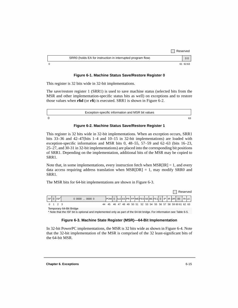
Chapter 6. Exceptions 6-15
Figure 6-1. Machine Status Save/Restore Register 0
This register is 32 bits wide in 32-bit implementations.
The save/restore register 1 (SRR1) is used to save machine status (selected bits from theMSR and other implementation-specific status bits as well) on exceptions and to restorethose values when rfid (or rfi) is executed. SRR1 is shown in Figure 6-2.
Figure 6-2. Machine Status Save/Restore Register 1
This register is 32 bits wide in 32-bit implementations. When an exception occurs, SRR1bits 33–36 and 42–47(bits 1–4 and 10–15 in 32-bit implementations) are loaded withexception-specific information and MSR bits 0, 48–55, 57–59 and 62–63 (bits 16–23,25–27, and 30-31 in 32-bit implementations) are placed into the corresponding bit positionsof SRR1. Depending on the implementation, additional bits of the MSR may be copied toSRR1.
Note that, in some implementations, every instruction fetch when MSR[IR] = 1, and everydata access requiring address translation when MSR[DR] = 1, may modify SRR0 andSRR1.
The MSR bits for 64-bit implementations are shown in Figure 6-3.
Figure 6-3. Machine State Register (MSR)—64-Bit Implementation
In 32-bit PowerPC implementations, the MSR is 32 bits wide as shown in Figure 6-4. Notethat the 32-bit implementation of the MSR is comprised of the 32 least-significant bits ofthe 64-bit MSR.
SRR0 (holds EA for instruction in interrupted program flow)
0 61 62163
0 0
Reserved
0 63
Exception-specific information and MSR bit values
0 1 2 3 44 45 46 47 48 49 50 51 52 53 54 55 56 57 58 59 60 61 62 63
Reserved
POW 0 ILE EE PR FP ME FE0 SE BE FE1 0 IP IR DR 00 RI LESF 0 ISF* 0 0000 ... 0000 0
Temporary 64-Bit Bridge* Note that the ISF bit is optional and implemented only as part of the 64-bit bridge. For information see Table 6-5.

6-16 PowerPC Microprocessor Family: The Programming Environments, Rev. 1
Figure 6-4. Machine State Register (MSR)—32-Bit Implementation
Table 6-5 shows the bit definitions for the MSR.
Table 6-5. MSR Bit Settings
Bit(s)Name Description
64 Bit 32 Bit
0 — SF Sixty-four bit mode0 The 64-bit processor runs in 32-bit mode.1 The 64-bit processor runs in 64-bit mode. Note that this is the default setting.
1 — — Reserved
64-BIT BRIDGE
2— ISF Exception sixty-four bit mode (optional). When an exception occurs, this bit is
copied into MSR[SF] to select 64- or 32-bit mode for the context established by the exception.Note: If the function is not implemented, this bit is treated as reserved.
3–44 0–12 — Reserved
45 13 POW Power management enable0 Power management disabled (normal operation mode)1 Power management enabled (reduced power mode)Note: Power management functions are implementation-dependent. If the function is not implemented, this bit is treated as reserved.
46 14 — Reserved
47 15 ILE Exception little-endian mode. When an exception occurs, this bit is copied into MSR[LE] to select the endian mode for the context established by the exception.
48 16 EE External interrupt enable 0 While the bit is cleared the processor delays recognition of external
interrupts and decrementer exception conditions. 1 The processor is enabled to take an external interrupt or the decrementer
exception.
49 17 PR Privilege level 0 The processor can execute both user- and supervisor-level instructions.1 The processor can only execute user-level instructions.
50 18 FP Floating-point available 0 The processor prevents dispatch of floating-point instructions, including
floating-point loads, stores, and moves.1 The processor can execute floating-point instructions.
51 19 ME Machine check enable 0 Machine check exceptions are disabled. 1 Machine check exceptions are enabled.
0 12 13 14 15 16 17 18 19 20 21 22 23 24 252627282930 31
Reserved
0000 0000 0000 0 POW 0 ILE EE PR FP ME FE0 SE BE FE1 0 IP IR DR 00 RI LE
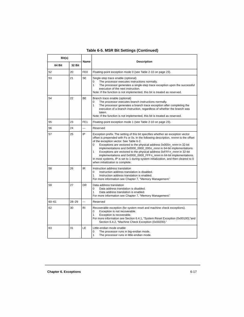
Chapter 6. Exceptions 6-17
52 20 FE0 Floating-point exception mode 0 (see Table 2-10 on page 23).
53 21 SE Single-step trace enable (optional)0 The processor executes instructions normally. 1 The processor generates a single-step trace exception upon the successful
execution of the next instruction.Note: If the function is not implemented, this bit is treated as reserved.
54 22 BE Branch trace enable (optional)0 The processor executes branch instructions normally. 1 The processor generates a branch trace exception after completing the
execution of a branch instruction, regardless of whether the branch was taken.
Note: If the function is not implemented, this bit is treated as reserved.
55 23 FE1 Floating-point exception mode 1 (see Table 2-10 on page 23).
56 24 — Reserved
57 25 IP Exception prefix. The setting of this bit specifies whether an exception vector offset is prepended with Fs or 0s. In the following description, nnnnn is the offset of the exception vector. See Table 6-2.0 Exceptions are vectored to the physical address 0x000n_nnnn in 32-bit
implementations and 0x0000_0000_000n_nnnn in 64-bit implementations.1 Exceptions are vectored to the physical address 0xFFFn_nnnn in 32-bit
implementations and 0x0000_0000_FFFn_nnnn in 64-bit implementations.In most systems, IP is set to 1 during system initialization, and then cleared to 0 when initialization is complete.
58 26 IR Instruction address translation 0 Instruction address translation is disabled. 1 Instruction address translation is enabled.For more information see Chapter 7, “Memory Management.”
59 27 DR Data address translation 0 Data address translation is disabled. 1 Data address translation is enabled.For more information see Chapter 7, “Memory Management.”
60–61 28–29 — Reserved
62 30 RI Recoverable exception (for system reset and machine check exceptions).0 Exception is not recoverable. 1 Exception is recoverable.For more information see Section 6.4.1, “System Reset Exception (0x00100),”and
Section 6.4.2, “Machine Check Exception (0x00200).”
63 31 LE Little-endian mode enable0 The processor runs in big-endian mode. 1 The processor runs in little-endian mode.
Table 6-5. MSR Bit Settings (Continued)
Bit(s)Name Description
64 Bit 32 Bit
6-18 PowerPC Microprocessor Family: The Programming Environments, Rev. 1
Those MSR bits that are written to SRR1 are written when the first instruction of theexception handler is encountered. The data address register (DAR) is used by severalexceptions (for example, DSI and alignment exceptions) to identify the address of amemory element.
6.2.1 Enabling and Disabling ExceptionsWhen a condition exists that may cause an exception to be generated, it must be determinedwhether the exception is enabled for that condition as follows:
• IEEE floating-point enabled exceptions (a type of program exception) are ignored when both MSR[FE0] and MSR[FE1] are cleared. If either of these bits is set, all IEEE enabled floating-point exceptions are taken and cause a program exception.
• Asynchronous, maskable exceptions (that is, the external and decrementer interrupts) are enabled by setting the MSR[EE] bit. When MSR[EE] = 0, recognition of these exception conditions is delayed. MSR[EE] is cleared automatically when an exception is taken, to delay recognition of conditions causing those exceptions.
• A machine check exception can only occur if the machine check enable bit, MSR[ME], is set. If MSR[ME] is cleared, the processor goes directly into checkstop state when a machine check exception condition occurs.
TEMPORARY 64-BIT BRIDGE
Bit 2 of the MSR (MSR[ISF]) may optionally be used by a 64-bit implementation tocontrol the mode (64-bit or 32-bit) that is entered when an exception is taken. If this bit isimplemented, it has the following properties:
• When an exception is taken, the value of MSR[ISF] is copied to MSR[SF].
• When an exception is taken, MSR[ISF] is not altered.
• No software synchronization is required before or after altering MSR[ISF]. Refer to Section 2.3.18, “Synchronization Requirements for Special Registers and for Lookaside Buffers,” for more information on synchronization requirements for altering other bits in the MSR.
If the MSR[ISF] bit is not implemented, it is treated as reserved except that the value isassumed to be 1 for exception processing.
Chapter 6. Exceptions 6-19
6.2.2 Steps for Exception Processing After it is determined that the exception can be taken (by confirming that any instruction-caused exceptions occurring earlier in the instruction stream have been handled, and byconfirming that the exception is enabled for the exception condition), the processor doesthe following:
1. The machine status save/restore register 0 (SRR0) is loaded with an instruction address that depends on the type of exception. See the individual exception description for details about how this register is used for specific exceptions.
2. SRR1 bits 33–36 and 42–47(bits 1–4 and 10–15 in 32-bit implementations) are loaded with information specific to the exception type.
3. MSR bits 0, 48–55, 57–59 and 62–63 (bits 16–23, 25–27, and 30-31 in 32-bit implementations) are loaded with a copy of the corresponding bits of the MSR. Note that depending on the implementation, additional bits from the MSR may be saved in SRR1.
4. The MSR is set as described in Table 6-6. The new values take effect beginning with the fetching of the first instruction of the exception-handler routine located at the exception vector address.
Note that MSR[IR] and MSR[DR] are cleared for all exception types; therefore, address translation is disabled for both instruction fetches and data accesses beginning with the first instruction of the exception-handler routine.
Also, note that the MSR[ILE] bit setting at the time of the exception is copied to MSR[LE] when the exception is taken (as shown in Table 6-6).
5. Instruction fetch and execution resumes, using the new MSR value, at a location specific to the exception type. The location is determined by adding the exception's vector offset (see Table 6-2) to the base address determined by MSR[IP]. If IP is cleared, exceptions are vectored to the physical address 0x0000_0000_000n_nnnn in 64-bit implementations and 0x000n_nnnn in 32-bit implementations. If IP is set, exceptions are vectored to the physical address 0x0000_0000_FFFn_nnnn in 64-bit implementations and 0xFFFn_nnnn in 32-bit implementations. For a machine check exception that occurs when MSR[ME] = 0 (machine check exceptions are disabled), the checkstop state is entered (the machine stops executing instructions). See Section 6.4.2, “Machine Check Exception (0x00200).”
In some implementations, any instruction fetch with MSR[IR] = 1 and any load or storewith MSR[DR] = 1 may cause SRR0 and SRR1 to be modified.
TEMPORARY 64-BIT BRIDGE
Similar to MSR[ILE], the MSR[ISF] bit setting at the time of the exception is copied to MSR[SF] when the exception is taken (if the ISF bit is implemented).
6-20 PowerPC Microprocessor Family: The Programming Environments, Rev. 1
6.2.3 Returning from an Exception HandlerThe Return from Interrupt (rfid [or rfi]) instruction performs context synchronization byallowing previously issued instructions to complete before returning to the interruptedprocess. Execution of the rfid (or rfi) instruction ensures the following:
• All previous instructions have completed to a point where they can no longer cause an exception.
If a previous instruction causes a direct-store interface error exception, the results are determined before this instruction is executed. However, note that the direct-store facility is being phased out of the architecture and will not likely be supported in future devices.
• Previous instructions complete execution in the context (privilege, protection, and address translation) under which they were issued.
• The rfid (or rfi) instruction copies SRR1 bits back into the MSR.
• The instructions following this instruction execute in the context established by this instruction.
For a complete description of context synchronization, refer to Section 6.1.2.1, “ContextSynchronization.”
TEMPORARY 64-BIT BRIDGE
The 64-bit bridge facility affects the operation of the return from exception mechanism inthat the rfi instruction can optionally be allowed to execute in 64-bit implementations. Inthis case, the mtmsr instruction must also be implemented. When these instructions areimplemented on a 64-bit implementation, their operation is identical to their operation ina 32-bit implementation. For an rfi instruction, in addition to the actions described above,the following occurs:
• The SRR1 bits that are copied to the corresponding bits of the MSR are bits 48–55, 57–59 and 62–63 of SRR1. Note that depending on the implementation, additional bits from SRR1 may be restored to the MSR. The remaining bits of the MSR, including the high-order 32 bits are unchanged.
• If the new MSR value does not enable any pending exceptions, then the next instruction is fetched, under control of the new MSR value from the address specified in SRR0[0–61] concatenated with 0b00 (when MSR[SF] = 1 in the new MSR value). Alternately, when MSR[SF] = 0 in the new MSR value, the next instruction is fetched from the address specified by thirty-two 0’s concatenated with SRR0[32–61], concatenated with 0b00.

Chapter 6. Exceptions 6-21
6.3 Process SwitchingThe operating system should execute the following when processes are switched:
• The sync instruction, which orders the effects of instruction execution. All instructions previously initiated appear to have completed before the sync instruction completes, and no subsequent instructions appear to be initiated until the sync instruction completes.
• The isync instruction, which waits for all previous instructions to complete and then discards any fetched instructions, causing subsequent instructions to be fetched (or refetched) from memory and to execute in the context (privilege, translation, protection, etc.) established by the previous instructions.
• The stwcx./stdcx. instruction, to clear any outstanding reservations, which ensures that an lwarx/ldarx instruction in the old process is not paired with an stwcx./stdcx. instruction in the new process.
The operating system should handle MSR[RI] as follows:
• In machine check and system reset exception handlers—If the SRR1 bit corresponding to MSR[RI] is cleared, the exception is not recoverable.
• In each exception handler—When enough state information has been saved that a machine check or system reset exception can reconstruct the previous state, set MSR[RI].
• At the end of each exception handler—Clear MSR[RI], set the SRR0 and SRR1 registers appropriately, and then execute rfid (or rfi).
Note that the RI bit being set indicates that, with respect to the processor, enough processorstate data is valid for the processor to continue, but it does not guarantee that the interruptedprocess can resume.

6-22 PowerPC Microprocessor Family: The Programming Environments, Rev. 1
6.4 Exception DefinitionsTable 6-6 shows all the types of exceptions that can occur and certain MSR bit settingswhen the exception handler is invoked. Depending on the exception, certain of these bitsare stored in SRR1 when an exception is taken. The following subsections describe eachexception in detail.
Table 6-6. MSR Setting Due to Exception
Exception Type
MSR Bit
SF1,2 ISF2 POW ILE EE PR FP ME FE0 SE BE FE1 IP IR DR RI LE
System reset 1 — 0 — 0 0 0 — 0 0 0 0 — 0 0 0 ILE
Machine check 1 — 0 — 0 0 0 0 0 0 0 0 — 0 0 0 ILE
DSI 1 — 0 — 0 0 0 — 0 0 0 0 — 0 0 0 ILE
ISI 1 — 0 — 0 0 0 — 0 0 0 0 — 0 0 0 ILE
External 1 — 0 — 0 0 0 — 0 0 0 0 — 0 0 0 ILE
Alignment 1 — 0 — 0 0 0 — 0 0 0 0 — 0 0 0 ILE
Program 1 — 0 — 0 0 0 — 0 0 0 0 — 0 0 0 ILE
Floating-point unavailable
1 — 0 — 0 0 0 — 0 0 0 0 — 0 0 0 ILE
Decrementer 1 — 0 — 0 0 0 — 0 0 0 0 — 0 0 0 ILE
System call 1 — 0 — 0 0 0 — 0 0 0 0 — 0 0 0 ILE
Trace exception
1 — 0 — 0 0 0 — 0 0 0 0 — 0 0 0 ILE
Floating-point assist exception
1 — 0 — 0 0 0 — 0 0 0 0 — 0 0 0 ILE
0 Bit is cleared.1 Bit is set.ILE Bit is copied from the ILE bit in the MSR.— Bit is not altered.Reading of reserved bits may return 0, even if the value last written to it was 1.
164-bit implementations only.
TEMPORARY 64-BIT BRIDGE2 When the 64-bit bridge is implemented in a 64-bit processor and the MSR[ISF] bit is implemented, the value of the MSR[ISF] bit is copied to the MSR[SF] bit when an exception is taken.

Chapter 6. Exceptions 6-23
6.4.1 System Reset Exception (0x00100)The system reset exception is a nonmaskable, asynchronous exception signaled to theprocessor typically through the assertion of a system-defined signal; see Table 6-7.
When a system reset exception is taken, instruction execution continues at offset 0x00100from the physical base address determined by MSR[IP].
If the exception is recoverable, the value of the MSR[RI] bit is copied to the correspondingSRR1 bit. The exception functions as a context-synchronizing operation. If a resetexception causes the loss of:
• an external exception (interrupt or decrementer),• direct-store error type DSI (the direct-store facility is being phased out of the
architecture—not likely to be supported in future devices), or• floating-point enabled type program exception,
then the exception is not recoverable. If the SRR1 bit corresponding to MSR[RI] is cleared,the exception is context-synchronizing only with respect to subsequent instructions. Notethat each implementation provides a means for software to distinguish between power-onreset and other types of system resets (such as soft reset).
Table 6-7. System Reset Exception—Register Settings
Register Setting Description
SRR0 Set to the effective address of the instruction that the processor would have attempted to execute next if no exception conditions were present.
SRR1 64-Bit 32-Bit0 —33–36 1–442–47 10–1548–55 16–2357–59 25–2762 30
63 31
Loaded with equivalent bit from the MSRClearedClearedLoaded with equivalent bits from the MSRLoaded with equivalent bits from the MSRLoaded from the equivalent MSR bit, MSR[RI], if the exception is recoverable; otherwise cleared. Loaded with equivalent bit from the MSR
Note that depending on the implementation, additional bits in the MSR may be copied to SRR1.If the processor state is corrupted to the extent that execution cannot resume reliably, the bit corresponding to MSR[RI], (SRR1[62] in 64-bit implementations and SRR1[30] in 32-bit implementations), is cleared.
MSR SF * 1ISF * —POW 0ILE —EE 0
PR 0FP 0ME —FE0 0
SE 0BE 0FE1 0IP —
IR 0DR 0RI 0LE Set to value of ILE
TEMPORARY 64-BIT BRIDGE* 2 If the MSR[ISF] bit is implemented, the value of the MSR[ISF] bit is copied to the MSR[SF] bit when an exception is taken.

6-24 PowerPC Microprocessor Family: The Programming Environments, Rev. 1
6.4.2 Machine Check Exception (0x00200)If no higher-priority exception is pending (namely, a system reset exception), the processorinitiates a machine check exception when the appropriate condition is detected. Note thatthe causes of machine check exceptions are implementation- and system-dependent, andare typically signalled to the processor by the assertion of a specified signal on theprocessor interface.
When a machine check condition occurs and MSR[ME] = 1, the exception is recognizedand handled. If MSR[ME] = 0 and a machine check occurs, the processor generates aninternal checkstop condition. When a processor is in checkstop state, instruction processingis suspended and generally cannot continue without resetting the processor. Someimplementations may preserve some or all of the internal state of the processor whenentering the checkstop state, so that the state can be analyzed as an aid in problemdetermination.
In general, it is expected that a bus error signal would be used by a memory controller toindicate a memory parity error or an uncorrectable memory ECC error. Note that theresulting machine check exception has priority over any exceptions caused by theinstruction that generated the bus operation.
If a machine check exception causes an exception that is not context-synchronizing, theexception is not recoverable. Also, a machine check exception is not recoverable if it causesthe loss of one of the following:
• An external exception (interrupt or decrementer)
• Direct-store error type DSI (the direct-store facility is being phased out of the architecture and is not likely to be supported in future devices)
• Floating-point enabled type program exception
If the SRR1 bit corresponding to MSR[RI] is cleared, the exception is context-synchronizing only with respect to subsequent instructions. If the exception is recoverable,the SRR1 bit corresponding to MSR[RI] is set and the exception is context-synchronizing.
Note that if the error is caused by the memory subsystem, incorrect data could be loadedinto the processor and register contents could be corrupted regardless of whether theexception is considered recoverable by the SRR1 bit corresponding to MSR[RI].
On some implementations, a machine check exception may be caused by referring to anonexistent physical (real) address, either because translation is disabled (MSR[IR] orMSR[DR] = 0) or through an invalid translation. On such a system, execution of the dcbzor dcba instruction can cause a delayed machine check exception by introducing a blockinto the data cache that is associated with an invalid physical (real) address. A machinecheck exception could eventually occur when and if a subsequent attempt is made to storethat block to memory (for example, as the block becomes the target for replacement, or asthe result of executing a dcbst instruction).

Chapter 6. Exceptions 6-25
When a machine check exception is taken, registers are updated as shown in Table 6-8.
If MSR[RI] is set, the machine check exception may still be unrecoverable in the sense thatexecution cannot resume in the same context that existed before the exception.
When a machine check exception is taken, instruction execution resumes at offset 0x00200from the physical base address determined by MSR[IP].
6.4.3 DSI Exception (0x00300)A DSI exception occurs when no higher priority exception exists and a data memory accesscannot be performed. The condition that caused the DSI exception can be determined byreading the DSISR, a supervisor-level SPR (SPR18) that can be read by using the mfsprinstruction. Bit settings are provided in Table 6-9. Table 6-9 also indicates which memoryelement is pointed to by the DAR. DSI exceptions can be generated by load/storeinstructions, cache-control instructions (icbi, dcbi, dcbz, dcbst, and dcbf), or theeciwx/ecowx instructions for any of the following reasons:
• A load or a store instruction results in a direct-store error exception. Note that the direct-store facility is being phased out of the architecture and is not likely to be supported in future devices.
• The effective address cannot be translated. That is, there is a page fault for this portion of the translation, so a DSI exception must be taken to retrieve the translation, for example from a storage device such as a hard disk drive.
Table 6-8. Machine Check Exception—Register Settings
Register Setting Description
SRR0 On a best-effort basis, implementations can set this to an EA of some instruction that was executing or about to be executing when the machine check condition occurred.
SRR1 Bit 62 (bit 30 in 32-bit implementations) is loaded from MSR[RI] if the processor is in a recoverable state. Otherwise cleared. The setting of all other SRR1 bits is implementation-dependent.
MSR SF 1 1ISF 1 —POW 0ILE —EE 0
PR 0FP 0ME 2 —FE0 0
SE 0BE 0FE1 0IP —
IR 0DR 0RI 0LE Set to value of ILE
TEMPORARY 64-BIT BRIDGE1 If the MSR[ISF] bit is implemented, the value of the MSR[ISF] bit is copied to the MSR[SF] bit when an
exception is taken
2 Note that when a machine check exception is taken, the exception handler should set MSR[ME] as soon as it is practical to handle another machine check exception. Otherwise, subsequent machine check exceptions cause the processor to automatically enter the checkstop state.

6-26 PowerPC Microprocessor Family: The Programming Environments, Rev. 1
• The instruction is not supported for the type of memory addressed.
— For lwarx/stwcx. and ldarx/stdcx. instructions that reference a memory location that is write-through required. If the exception is not taken, the instructions execute correctly.
— For lwarx/stwcx., ldarx/stdcx., or eciwx/ecowx instructions that attempt to access direct-store segments (direct-store facility is being phased out of the architecture—not likely to be supported in future devices). If the exception does not occur, the results are boundedly undefined.
• The access violates memory protection.
• The execution of an eciwx or ecowx instruction is disallowed because the external access register enable bit (EAR[E]) is cleared.
• A data address breakpoint register (DABR) match occurs. The DABR facility is optional to the PowerPC architecture, but if one is implemented, it is recommended, but not required, that it be implemented as follows. A data address breakpoint match is detected for a load or store instruction if the three following conditions are met for any byte accessed:
— EA[0–60] (EA[0–28] in 32-bit implementations) = DABR[DAB]
— MSR[DR] = DABR[BT]
— The instruction is a store and DABR[DW] = 1, or the instruction is a load and DABR[DR] = 1.
The DABR is described in Section 2.3.15, “Data Address Breakpoint Register (DABR).” In 32-bit mode of 64-bit implementations, the high-order 32 bits of the EA are treated as zero for the purpose of detecting a match; the DAR settings are described in Table 6-9. If the above conditions are satisfied, it is undefined whether a match occurs in the following cases:
— The instruction is store conditional but the store is not performed.
— The instruction is a load/store string of zero length.
— The instruction is dcbz, eciwx, or ecowx.
The cache management instructions other than dcbz never cause a match. If dcbz causes a match, some or all of the target memory locations may have been updated. For the purpose of determining whether a match occurs, eciwx is treated as a load, and ecowx and dcbz are treated as stores.
If an stwcx./stdcx. instruction has an EA for which a normal store operation would causea DSI exception but the processor does not have the reservation from lwarx/ldarx, whethera DSI exception is taken is implementation-dependent.
If the value in XER[25–31] indicates that a load or store string instruction has a length ofzero, a DSI exception does not occur, regardless of the effective address.

Chapter 6. Exceptions 6-27
The condition that caused the exception is defined in the DSISR. As shown in Table 6-9,this exception also sets the data address register (DAR).
Table 6-9. DSI Exception—Register Settings
Register Setting Description
SRR0 Set to the effective address of the instruction that caused the exception.
SRR1 64-Bit 32-Bit0 —33–36 1–442–47 10–1548–55 16–2357–59 25–2762–63 30–31
Loaded with equivalent bit from the MSRClearedClearedLoaded with equivalent bits from the MSRLoaded with equivalent bits from the MSRLoaded with equivalent bits from the MSR
Note that depending on the implementation, additional bits in the MSR may be copied to SRR1.
MSR SF * 1ISF * —POW 0ILE —EE 0
PR 0FP 0ME —FE0 0
SE 0BE 0FE1 0IP —
IR 0DR 0RI 0LE Set to value of ILE
TEMPORARY 64-BIT BRIDGE* If the MSR[ISF] bit is implemented, the value of the MSR[ISF] bit is copied to the MSR[SF] bit when an
exception is taken.
DSISR 0 Set if a load or store instruction results in a direct-store error exception; otherwise cleared. Note that the direct-store facility is being phased out of the architecture and is not likely to be supported in future devices.
1 Set if the translation of an attempted access is not found in the primary hash table entry group (HTEG), or in the rehashed secondary HTEG, or in the range of a DBAT register (page fault condition); otherwise cleared.
2–3 Cleared4 Set if a memory access is not permitted by the page or DBAT protection mechanism; otherwise
cleared. 5 Set if the eciwx, ecowx, lwarx/ldarx, or stwcx./stdcx. instruction is attempted to direct-store
interface space, or if the lwarx/ldarx or stwcx./stdcx. instruction is used with addresses that are marked as write-through. Otherwise cleared to 0. Note that the direct-store facility is being phased out of the architecture and is not likely to be supported in future devices.
6 Set for a store operation and cleared for a load operation. 7–8 Cleared9 Set if a DABR match occurs. Otherwise cleared.10 For 64-bit implementations, set if the segment table search fails to find a translation for the
effective address (segment fault condition); otherwise cleared. Cleared in 32-bit implementations.
11 Set if the instruction is an eciwx or ecowx and EAR[E] = 0; otherwise cleared.12–31 ClearedDue to the multiple exception conditions possible from the execution of a single instruction, the following combinations of bits of DSISR may be set concurrently:• Bits 1 and 11• Bits 4 and 5• Bits 4 and 11• Bits 5 and 11• Bits 10 and 11
Additonally, bit 6 is set if the instruction that caused the exception is a store, ecowx, dcbz, dcba, or dcbi and bit 6 would otherwise be cleared. Also, bit 9 (DABR match) may be set alone, or in combination with any other bit, or with any of the other combinations shown above.
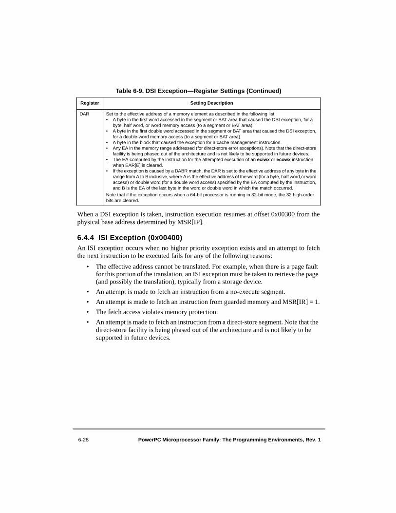
6-28 PowerPC Microprocessor Family: The Programming Environments, Rev. 1
When a DSI exception is taken, instruction execution resumes at offset 0x00300 from thephysical base address determined by MSR[IP].
6.4.4 ISI Exception (0x00400)An ISI exception occurs when no higher priority exception exists and an attempt to fetchthe next instruction to be executed fails for any of the following reasons:
• The effective address cannot be translated. For example, when there is a page fault for this portion of the translation, an ISI exception must be taken to retrieve the page (and possibly the translation), typically from a storage device.
• An attempt is made to fetch an instruction from a no-execute segment.
• An attempt is made to fetch an instruction from guarded memory and MSR[IR] = 1.
• The fetch access violates memory protection.
• An attempt is made to fetch an instruction from a direct-store segment. Note that the direct-store facility is being phased out of the architecture and is not likely to be supported in future devices.
DAR Set to the effective address of a memory element as described in the following list:• A byte in the first word accessed in the segment or BAT area that caused the DSI exception, for a
byte, half word, or word memory access (to a segment or BAT area).• A byte in the first double word accessed in the segment or BAT area that caused the DSI exception,
for a double-word memory access (to a segment or BAT area).• A byte in the block that caused the exception for a cache management instruction.• Any EA in the memory range addressed (for direct-store error exceptions). Note that the direct-store
facility is being phased out of the architecture and is not likely to be supported in future devices.• The EA computed by the instruction for the attempted execution of an eciwx or ecowx instruction
when EAR[E] is cleared.• If the exception is caused by a DABR match, the DAR is set to the effective address of any byte in the
range from A to B inclusive, where A is the effective address of the word (for a byte, half word,or word access) or double word (for a double word access) specified by the EA computed by the instruction, and B is the EA of the last byte in the word or double word in which the match occurred.
Note that if the exception occurs when a 64-bit processor is running in 32-bit mode, the 32 high-order bits are cleared.
Table 6-9. DSI Exception—Register Settings (Continued)
Register Setting Description
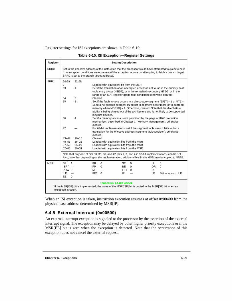
Chapter 6. Exceptions 6-29
Register settings for ISI exceptions are shown in Table 6-10.
When an ISI exception is taken, instruction execution resumes at offset 0x00400 from thephysical base address determined by MSR[IP].
6.4.5 External Interrupt (0x00500)An external interrupt exception is signaled to the processor by the assertion of the externalinterrupt signal. The exception may be delayed by other higher priority exceptions or if theMSR[EE] bit is zero when the exception is detected. Note that the occurrance of thisexception does not cancel the external request.
Table 6-10. ISI Exception—Register Settings
Register Setting Description
SRR0 Set to the effective address of the instruction that the processor would have attempted to execute next if no exception conditions were present (if the exception occurs on attempting to fetch a branch target, SRR0 is set to the branch target address).
SRR1 64-Bit 32-Bit0 —33 1
34 235 3
36 4
42 —
43–47 10–1548–55 16–2357–59 25–2762–63 30–31
Loaded with equivalent bit from the MSRSet if the translation of an attempted access is not found in the primary hash table entry group (HTEG), or in the rehashed secondary HTEG, or in the range of an IBAT register (page fault condition); otherwise cleared. ClearedSet if the fetch access occurs to a direct-store segment (SR[T] = 1 or STE = 1), to a no-execute segment (N bit set in segment descriptor), or to guarded memory when MSR[IR] = 1. Otherwise, cleared. Note that the direct-store facility is being phased out of the architecture and is not likely to be supported in future devices.Set if a memory access is not permitted by the page or IBAT protection mechanism, described in Chapter 7, “Memory Management”; otherwise cleared. For 64-bit implementations, set if the segment table search fails to find a translation for the effective address (segment fault condition); otherwise cleared. Cleared Loaded with equivalent bits from the MSRLoaded with equivalent bits from the MSRLoaded with equivalent bits from the MSR
Note that only one of bits 33, 35, 36, and 42 (bits 1, 3, and 4 in 32-bit implementations) can be set . Also, note that depending on the implementation, additional bits in the MSR may be copied to SRR1.
MSR SF * 1ISF * —POW 0ILE —EE 0
PR 0FP 0ME —FE0 0
SE 0BE 0FE1 0IP —
IR 0DR 0RI 0LE Set to value of ILE
TEMPORARY 64-BIT BRIDGE* If the MSR[ISF] bit is implemented, the value of the MSR[ISF] bit is copied to the MSR[SF] bit when an
exception is taken.
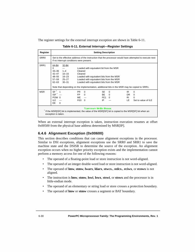
6-30 PowerPC Microprocessor Family: The Programming Environments, Rev. 1
The register settings for the external interrupt exception are shown in Table 6-11.
When an external interrupt exception is taken, instruction execution resumes at offset0x00500 from the physical base address determined by MSR[IP].
6.4.6 Alignment Exception (0x00600)This section describes conditions that can cause alignment exceptions in the processor.Similar to DSI exceptions, alignment exceptions use the SRR0 and SRR1 to save themachine state and the DSISR to determine the source of the exception. An alignmentexception occurs when no higher priority exception exists and the implementation cannotperform a memory access for one of the following reasons:
• The operand of a floating-point load or store instruction is not word-aligned.
• The operand of an integer double-word load or store instruction is not word-aligned.
• The operand of lmw, stmw, lwarx, ldarx, stwcx., stdcx., eciwx, or ecowx is not aligned.
• The instruction is lmw, stmw, lswi, lswx, stswi, or stswx and the processor is in little-endian mode.
• The operand of an elementary or string load or store crosses a protection boundary.
• The operand of lmw or stmw crosses a segment or BAT boundary.
Table 6-11. External Interrupt—Register Settings
Register Setting Description
SRR0 Set to the effective address of the instruction that the processor would have attempted to execute next if no interrupt conditions were present.
SRR1 64-Bit 32-Bit0 —33–36 1–442–47 10–1548–55 16–2357–59 25–2762–63 30–31
Loaded with equivalent bit from the MSRClearedClearedLoaded with equivalent bits from the MSRLoaded with equivalent bits from the MSRLoaded with equivalent bits from the MSR
Note that depending on the implementation, additional bits in the MSR may be copied to SRR1.
MSR SF * 1ISF * —POW 0ILE —EE 0
PR 0FP 0ME —FE0 0
SE 0BE 0FE1 0IP —
IR 0DR 0RI 0LE Set to value of ILE
TEMPORARY 64-BIT BRIDGE* If the MSR[ISF] bit is implemented, the value of the MSR[ISF] bit is copied to the MSR[SF] bit when an
exception is taken.

Chapter 6. Exceptions 6-31
• The operand of dcbz is in memory that is write-through-required or caching inhibited, or dcbz is executed in an implementation that has either no data cache or a write-through data cache.
• The operand of a floating-point load or store instruction is in a direct-store segment (T = 1). Note that the direct-store facility is being phased out of the architecture and is not likely to be supported in future devices.
For lmw, stmw, lswi, lswx, stswi, and stswx instructions in little-endian mode, analignment exception always occurs. For lmw and stmw instructions with an operand that isnot aligned in big-endian mode, and for lwarx, ldarx, stwcx., stdcx., eciwx, and ecowxwith an operand that is not aligned in either endian mode, an implementation may yieldboundedly-undefined results instead of causing an alignment exception (for eciwx andecowx when EAR[E] = 0, a third alternative is to cause a DSI exception). For all other caseslisted above, an implementation may execute the instruction correctly instead of causing analignment exception. For the dcbz instruction, correct execution means clearing each byteof the block in main memory. See Section 3.1, “Data Organization in Memory and DataTransfers,” for a complete definition of alignment in the PowerPC architecture.
The term, ‘protection boundary’, refers to the boundary between protection domains. Aprotection domain is a segment, a block of memory defined by a BAT entry, a virtual 4-Kbyte page, or a range of unmapped effective addresses. Protection domains are definedonly when the corresponding address translation (instruction or data) is enabled (MSR[IR]or MSR[DR] = 1).
The register settings for alignment exceptions are shown in Table 6-12.
Table 6-12. Alignment Exception—Register Settings
Register Setting Description
SRR0 Set to the effective address of the instruction that caused the exception.
SRR1 64-Bit 32-Bit0 —33–36 1–442–47 10–1548–55 16–2357–59 25–2762–63 30–31
Loaded with equivalent bit from the MSRClearedClearedLoaded with equivalent bits from the MSRLoaded with equivalent bits from the MSRLoaded with equivalent bits from the MSR
Note that depending on the implementation, additional bits in the MSR may be copied to SRR1.
MSR SF * 1ISF * —POW 0ILE —EE 0
PR 0FP 0ME —FE0 0
SE 0BE 0FE1 0IP —
IR 0DR 0RI 0LE Set to value of ILE

6-32 PowerPC Microprocessor Family: The Programming Environments, Rev. 1
The architecture does not support the use of a misaligned EA by load/store with reservationinstructions or by the eciwx and ecowx instructions. If one of these instructions specifies amisaligned EA, the exception handler should not emulate the instruction but should treatthe occurrence as a programming error.
DSISR 0–14 (32-bit implementations) Cleared 10–11 (64-bit implementations) Cleared 2–13 (64-bit implementations) For 64-bit instructions that use immediate addressing—set to bits 30
and 31. Otherwise cleared. 14 (64-bit implementations) Cleared15–16 For instructions that use register indirect with index addressing—set to bits 29–30 of the
instruction encoding.For instructions that use register indirect with immediate index addressing—cleared
17 For instructions that use register indirect with index addressing—set to bit 25 of the instruction encoding.For instructions that use register indirect with immediate index addressing— set to bit 5 of the instruction encoding.
18–21 For instructions that use register indirect with index addressing—set to bits 21–24 of the instruction encoding. For instructions that use register indirect with immediate index addressing—set to bits 1–4 of the instruction encoding.
22–26 Set to bits 6–10 (identifying either the source or destination) of the instruction encoding. Undefined for dcbz.
27–31 Set to bits 11–15 of the instruction encoding (rA) for update-form instructionsSet to either bits 11–15 of the instruction encoding or to any register number not in the range of registers loaded by a valid form instruction for lmw, lswi, and lswx instructions. Otherwise undefined.
Note that for load or store instructions that use register indirect with index addressing, the DSISR can be set to the same value that would have resulted if the corresponding instruction uses register indirect with immediate index addressing had caused the exception. Similarly, for load or store instructions that use register indirect with immediate index addressing, DSISR can hold a value that would have resulted from an instruction that uses register indirect with index addressing. For example, a misaligned lwarx instruction that crosses a protection boundary would normally cause the DSISR to be set to the following binary value:
000000000000 00 0 01 0 0101 ttttt ?????The value ttttt refers to the destination and ????? indicates undefined bits. However, this register may be set as if the instruction were lwa, as follows:000000000000 10 0 00 0 1101 ttttt ?????If there is no corresponding instruction (such as for the lwaux instruction), no alternative value can be specified.
The instruction pairs that can use the same DSISR values are as follows:lbz/lbzx lbzu/lbzux lhz/lhzx lhzu/lhzux lha/lhax lhau/lhaux lwz/lwzx lwzu/lwzux lwa/lwax ld/ldx ldu/ldux stb/stbxstbu/stbux sth/sthx sthu/sthux stw/stwx stwu/stwux std/stdxstdu/stdux lfs/lfsx lfsu/lfsux lfd/lfdx lfdu/lfdux stfs/stfsxstfsu/stfsux stfd/stfdx stfdu/stfdux
DAR Set to the EA of the data access as computed by the instruction causing the alignment exception. Note that if a 64-bit processor is running in 32-bit mode, the 32 high-order bits are cleared.
TEMPORARY 64-BIT BRIDGE* If the MSR[ISF] bit is implemented, the value of the MSR[ISF] bit is copied to the MSR[SF] bit when an
exception is taken.
Table 6-12. Alignment Exception—Register Settings (Continued)
Register Setting Description

Chapter 6. Exceptions 6-33
6.4.6.1 Integer Alignment Exceptions Operations that are not naturally aligned may suffer performance degradation, dependingon the processor design, the type of operation, the boundaries crossed, and the mode thatthe processor is in during execution. More specifically, these operations may either causean alignment exception or they may cause the processor to break the memory access intomultiple, smaller accesses with respect to the cache and the memory subsystem.
6.4.6.1.1 Page Address Translation Access ConsiderationsA page address translation access occurs when MSR[DR] is set, SR[T] is cleared, and thereis no BAT match. Note that a dcbz instruction causes an alignment exception if the accessis to a page or block with the W (write-through) or I (cache-inhibit) bit set.
Misaligned memory accesses that do not cause an alignment exception may not perform aswell as an aligned access of the same type. The resulting performance degradation due tomisaligned accesses depends on how well each individual access behaves with respect tothe memory hierarchy.
Particular details regarding page address translation is implementation-dependent; thereader should consult the user’s manual for the appropriate processor for more information.
6.4.6.1.2 Direct-Store Interface Access ConsiderationsThe following apply for direct-store interface accesses:
• If a 256-Mbyte boundary will be crossed by any portion of the direct-store interface space accessed by an instruction (the entire string for strings/multiples), an alignment exception is taken.
• Floating-point loads and stores to direct-store segments may cause an alignment exception, regardless of operand alignment.
• The load/store word/double word with reservation instructions that map into a direct-store segment always cause a DSI exception. However, if the instruction crosses a segment boundary an alignment exception is taken instead.
Note that the direct-store facility is being phased out of the architecture and is not likely tobe supported in future devices.
6.4.6.2 Little-Endian Mode Alignment ExceptionsThe OEA allows implementations to take alignment exceptions on misaligned accesses (asdescribed in Section 3.1.4, “PowerPC Byte Ordering”) in little-endian mode but does notrequire them to do so. Some implementations may perform some misaligned accesseswithout taking an alignment exception.

6-34 PowerPC Microprocessor Family: The Programming Environments, Rev. 1
6.4.6.3 Interpretation of the DSISR as Set by an Alignment ExceptionFor most alignment exceptions, an exception handler may be designed to emulate theinstruction that causes the exception. To do this, the handler requires the followingcharacteristics of the instruction:
• Load or store
• Length (half word, word, or double word)
• String, multiple, or normal load/store
• Integer or floating-point
• Whether the instruction performs update
• Whether the instruction performs byte reversal
• Whether it is a dcbz instruction
The PowerPC architecture provides this information implicitly, by setting opcode bits in theDSISR that identify the excepting instruction type. The exception handler does not need toload the excepting instruction from memory. The mapping for all exception possibilities isunique except for the few exceptions discussed below.
Table 6-13 shows the inverse mapping—how the DSISR bits identify the instruction thatcaused the exception.
The alignment exception handler cannot distinguish a floating-point load or store thatcauses an exception because it is misaligned, or because it addresses the direct-storeinterface space. However, this does not matter; in either case it is emulated with integerinstructions. Note that the direct-store facility is being phased out of the architecture and isnot likely to be supported in future devices.
Table 6-13. DSISR(15–21) Settings to Determine Misaligned Instruction
DSISR[15–21] Instruction DSISR[15–21] Instruction
00 0 0000 lwarx, lwz, special casesl1 01 1 0010 stdux
00 0 0010 ldarx 01 1 0101 lwaux
00 0 0010 stw 10 0 0010 stwcx.
00 0 0100 lhz 10 0 0011 stdcx.
00 0 0101 lha 10 0 1000 lwbrx
00 0 0110 sth 10 0 1010 stwbrx
00 0 0111 lmw 10 0 1100 lhbrx
00 0 1000 lfs 10 0 1110 sthbrx
00 0 1001 lfd 10 1 0100 eciwx
00 0 1010 stfs 10 1 0110 ecowx
00 0 1011 stfd 10 1 1111 dcbz
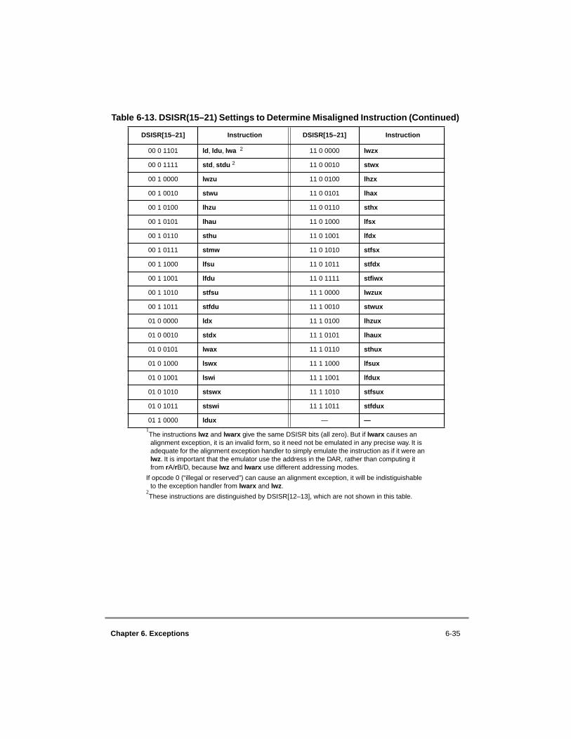
Chapter 6. Exceptions 6-35
00 0 1101 ld, ldu, lwa 2 11 0 0000 lwzx
00 0 1111 std, stdu 2 11 0 0010 stwx
00 1 0000 lwzu 11 0 0100 lhzx
00 1 0010 stwu 11 0 0101 lhax
00 1 0100 lhzu 11 0 0110 sthx
00 1 0101 lhau 11 0 1000 lfsx
00 1 0110 sthu 11 0 1001 lfdx
00 1 0111 stmw 11 0 1010 stfsx
00 1 1000 lfsu 11 0 1011 stfdx
00 1 1001 lfdu 11 0 1111 stfiwx
00 1 1010 stfsu 11 1 0000 lwzux
00 1 1011 stfdu 11 1 0010 stwux
01 0 0000 ldx 11 1 0100 lhzux
01 0 0010 stdx 11 1 0101 lhaux
01 0 0101 lwax 11 1 0110 sthux
01 0 1000 lswx 11 1 1000 lfsux
01 0 1001 lswi 11 1 1001 lfdux
01 0 1010 stswx 11 1 1010 stfsux
01 0 1011 stswi 11 1 1011 stfdux
01 1 0000 ldux — —1The instructions lwz and lwarx give the same DSISR bits (all zero). But if lwarx causes an alignment exception, it is an invalid form, so it need not be emulated in any precise way. It is adequate for the alignment exception handler to simply emulate the instruction as if it were an lwz. It is important that the emulator use the address in the DAR, rather than computing it from rA/rB/D, because lwz and lwarx use different addressing modes.
If opcode 0 (“illegal or reserved”) can cause an alignment exception, it will be indistiguishable to the exception handler from lwarx and lwz.
2These instructions are distinguished by DSISR[12–13], which are not shown in this table.
Table 6-13. DSISR(15–21) Settings to Determine Misaligned Instruction (Continued)
DSISR[15–21] Instruction DSISR[15–21] Instruction
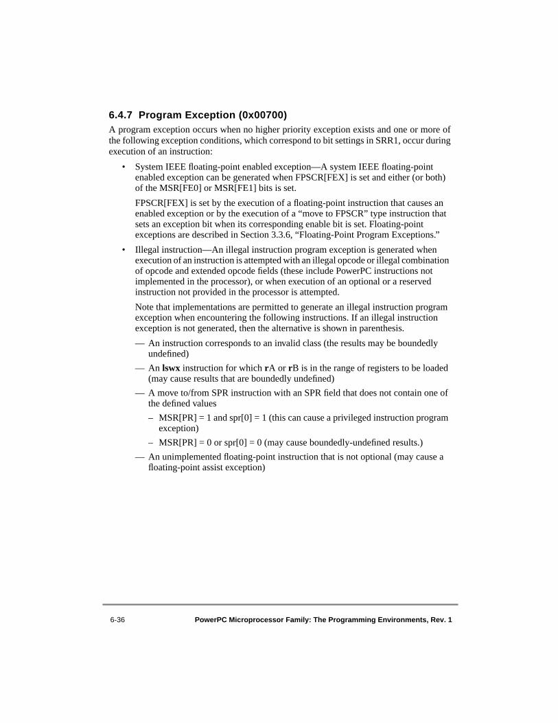
6-36 PowerPC Microprocessor Family: The Programming Environments, Rev. 1
6.4.7 Program Exception (0x00700) A program exception occurs when no higher priority exception exists and one or more ofthe following exception conditions, which correspond to bit settings in SRR1, occur duringexecution of an instruction:
• System IEEE floating-point enabled exception—A system IEEE floating-point enabled exception can be generated when FPSCR[FEX] is set and either (or both) of the MSR[FE0] or MSR[FE1] bits is set.
FPSCR[FEX] is set by the execution of a floating-point instruction that causes an enabled exception or by the execution of a “move to FPSCR” type instruction that sets an exception bit when its corresponding enable bit is set. Floating-point exceptions are described in Section 3.3.6, “Floating-Point Program Exceptions.”
• Illegal instruction—An illegal instruction program exception is generated when execution of an instruction is attempted with an illegal opcode or illegal combination of opcode and extended opcode fields (these include PowerPC instructions not implemented in the processor), or when execution of an optional or a reserved instruction not provided in the processor is attempted.
Note that implementations are permitted to generate an illegal instruction program exception when encountering the following instructions. If an illegal instruction exception is not generated, then the alternative is shown in parenthesis.
— An instruction corresponds to an invalid class (the results may be boundedly undefined)
— An lswx instruction for which rA or rB is in the range of registers to be loaded (may cause results that are boundedly undefined)
— A move to/from SPR instruction with an SPR field that does not contain one of the defined values
– MSR[PR] = 1 and spr[0] = 1 (this can cause a privileged instruction program exception)
– MSR[PR] = 0 or spr[0] = 0 (may cause boundedly-undefined results.)
— An unimplemented floating-point instruction that is not optional (may cause a floating-point assist exception)
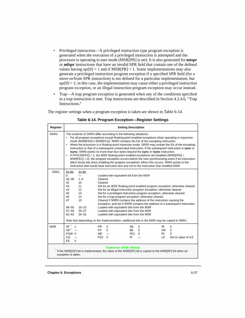
Chapter 6. Exceptions 6-37
• Privileged instruction—A privileged instruction type program exception is generated when the execution of a privileged instruction is attempted and the processor is operating in user mode (MSR[PR] is set). It is also generated for mtspr or mfspr instructions that have an invalid SPR field that contain one of the defined values having spr[0] = 1 and if MSR[PR] = 1. Some implementations may also generate a privileged instruction program exception if a specified SPR field (for a move to/from SPR instruction) is not defined for a particular implementation, but spr[0] = 1; in this case, the implementation may cause either a privileged instruction program exception, or an illegal instruction program exception may occur instead.
• Trap—A trap program exception is generated when any of the conditions specified in a trap instruction is met. Trap instructions are described in Section 4.2.4.6, “Trap Instructions.”
The register settings when a program exception is taken are shown in Table 6-14.
Table 6-14. Program Exception—Register Settings
Register Setting Description
SRR0 The contents of SRR0 differ according to the following situations:• For all program exceptions except floating-point enabled exceptions when operating in imprecise
mode (MSR[FE0] ≠ MSR[FE1]), SRR0 contains the EA of the excepting instruction.• When the processor is in floating-point imprecise mode, SRR0 may contain the EA of the excepting
instruction or that of a subsequent unexecuted instruction. If the subsequent instruction is sync or isync, SRR0 points no more than four bytes beyond the sync or isync instruction.
• If FPSCR[FEX] = 1, but IEEE floating-point enabled exceptions are disabled (MSR[FE0] = MSR[FE1] = 0), the program exception occurs before the next synchronizing event if an instruction alters those bits (thus enabling the program exception). When this occurs, SRR0 points to the instruction that would have executed next and not to the instruction that modified MSR.
SRR1 64-Bit 32-Bit0 —33–36 1–442 1043 1144 1245 1346 1447 15
48–55 16–2357–59 25–2762–63 30–31
Loaded with equivalent bit from the MSRClearedClearedSet for an IEEE floating-point enabled program exception; otherwise cleared.Set for an illegal instruction program exception; otherwise cleared. Set for a privileged instruction program exception; otherwise cleared.Set for a trap program exception; otherwise cleared.Cleared if SRR0 contains the address of the instruction causing the exception, and set if SRR0 contains the address of a subsequent instruction.Loaded with equivalent bits from the MSRLoaded with equivalent bits from the MSRLoaded with equivalent bits from the MSR
Note that depending on the implementation, additional bits in the MSR may be copied to SRR1.
MSR SF * 1ISF * —POW 0ILE —EE 0
PR 0FP 0ME —FE0 0
SE 0BE 0FE1 0IP —
IR 0DR 0RI 0LE Set to value of ILE
TEMPORARY 64-BIT BRIDGE* If the MSR[ISF] bit is implemented, the value of the MSR[ISF] bit is copied to the MSR[SF] bit when an
exception is taken.
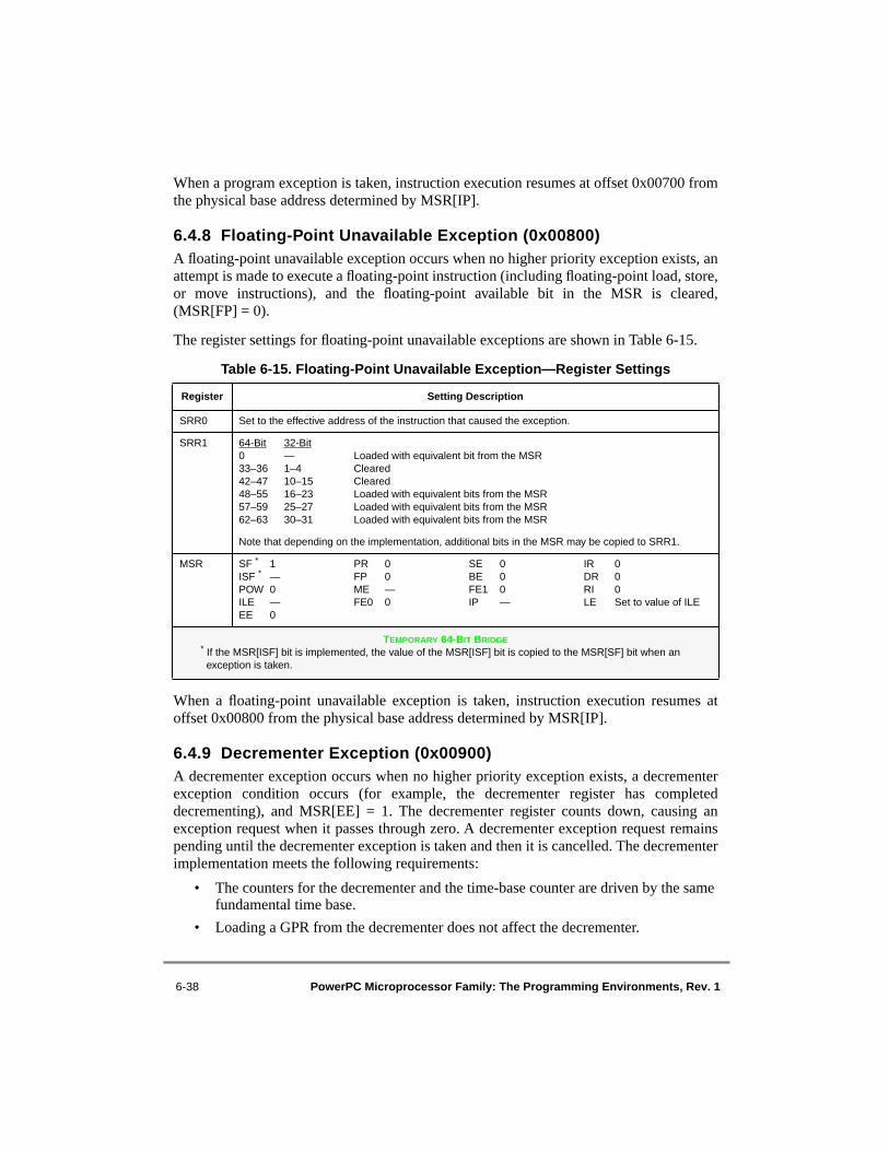
6-38 PowerPC Microprocessor Family: The Programming Environments, Rev. 1
When a program exception is taken, instruction execution resumes at offset 0x00700 fromthe physical base address determined by MSR[IP].
6.4.8 Floating-Point Unavailable Exception (0x00800)A floating-point unavailable exception occurs when no higher priority exception exists, anattempt is made to execute a floating-point instruction (including floating-point load, store,or move instructions), and the floating-point available bit in the MSR is cleared,(MSR[FP] = 0).
The register settings for floating-point unavailable exceptions are shown in Table 6-15.
When a floating-point unavailable exception is taken, instruction execution resumes atoffset 0x00800 from the physical base address determined by MSR[IP].
6.4.9 Decrementer Exception (0x00900)A decrementer exception occurs when no higher priority exception exists, a decrementerexception condition occurs (for example, the decrementer register has completeddecrementing), and MSR[EE] = 1. The decrementer register counts down, causing anexception request when it passes through zero. A decrementer exception request remainspending until the decrementer exception is taken and then it is cancelled. The decrementerimplementation meets the following requirements:
• The counters for the decrementer and the time-base counter are driven by the same fundamental time base.
• Loading a GPR from the decrementer does not affect the decrementer.
Table 6-15. Floating-Point Unavailable Exception—Register Settings
Register Setting Description
SRR0 Set to the effective address of the instruction that caused the exception.
SRR1 64-Bit 32-Bit0 —33–36 1–442–47 10–1548–55 16–2357–59 25–2762–63 30–31
Loaded with equivalent bit from the MSRClearedClearedLoaded with equivalent bits from the MSRLoaded with equivalent bits from the MSRLoaded with equivalent bits from the MSR
Note that depending on the implementation, additional bits in the MSR may be copied to SRR1.
MSR SF * 1ISF * —POW 0ILE —EE 0
PR 0FP 0ME —FE0 0
SE 0BE 0FE1 0IP —
IR 0DR 0RI 0LE Set to value of ILE
TEMPORARY 64-BIT BRIDGE* If the MSR[ISF] bit is implemented, the value of the MSR[ISF] bit is copied to the MSR[SF] bit when an
exception is taken.

Chapter 6. Exceptions 6-39
• Storing a GPR value to the decrementer replaces the value in the decrementer with the value in the GPR.
• Whenever bit 0 of the decrementer changes from 0 to 1, a decrementer exception request is signaled. If multiple decrementer exception requests are received before the first can be reported, only one exception is reported. The occurrence of a decrementer exception cancels the request.
• If the decrementer is altered by software and if bit 0 is changed from 0 to 1, an exception request is signaled.
The register settings for the decrementer exception are shown in Table 6-16.
When a decrementer exception is taken, instruction execution resumes at offset 0x00900from the physical base address determined by MSR[IP].
6.4.10 System Call Exception (0x00C00)A system call exception occurs when a System Call (sc) instruction is executed. Theeffective address of the instruction following the sc instruction is placed into SRR0. MSRbits are saved in SRR1, as shown in Table 6-17. Then a system call exception is generated.
Table 6-16. Decrementer Exception—Register Settings
Register Setting Description
SRR0 Set to the effective address of the instruction that the processor would have attempted to execute next if no exception conditions were present.
SRR1 64-Bit 32-Bit0 —33–36 1–442–47 10–1548–55 16–2357–59 25–2762–63 30–31
Loaded with equivalent bit from the MSRClearedClearedLoaded with equivalent bits from the MSRLoaded with equivalent bits from the MSRLoaded with equivalent bits from the MSR
Note that depending on the implementation, additional bits in the MSR may be copied to SRR1.
MSR SF * 1ISF * —POW 0ILE —EE 0
PR 0FP 0ME —FE0 0
SE 0BE 0FE1 0IP —
IR 0DR 0RI 0LE Set to value of ILE
TEMPORARY 64-BIT BRIDGE* If the MSR[ISF] bit is implemented, the value of the MSR[ISF] bit is copied to the MSR[SF] bit when an
exception is taken.

6-40 PowerPC Microprocessor Family: The Programming Environments, Rev. 1
The system call exception causes the next instruction to be fetched from offset 0x00C00from the physical base address determined by the new setting of MSR[IP]. As with mostother exceptions, this exception is context-synchronizing. Refer to Section 6.1.2.1,“Context Synchronization,” for more information on the actions performed by a context-synchronizing operation. Register settings are shown in Table 6-17.
When a system call exception is taken, instruction execution resumes at offset 0x00C00from the physical base address determined by MSR[IP].
6.4.11 Trace Exception (0x00D00)The trace exception is optional to the PowerPC architecture, and specific information abouthow it is implemented can be found in user’s manuals for individual processors.
The trace exception provides a means of tracing the flow of control of a program fordebugging and performance analysis purposes. It is controlled by MSR bits SE and BE asfollows:
• MSR[SE] = 1: the processor generates a single-step type trace exception after each instruction that completes without causing an exception or context change (such as occurs when an sc, rfid (or rfi), or a load instruction that causes an exception, for example, is executed).
• MSR[BE] = 1: the processor generates a branch-type trace exception after completing the execution of a branch instruction, whether or not the branch is taken.
Table 6-17. System Call Exception—Register Settings
Register Setting Description
SRR0 Set to the effective address of the instruction following the System Call instruction
SRR1 64-Bit 32-Bit0 —33–36 1–442–47 10–1548–55 16–2357–59 25–2762–63 30–31
Loaded with equivalent bit from the MSRClearedClearedLoaded with equivalent bits from the MSRLoaded with equivalent bits from the MSRLoaded with equivalent bits from the MSR
Note that depending on the implementation, additional bits in the MSR may be copied to SRR1.
MSR SF * 1ISF * —POW 0ILE —EE 0
PR 0FP 0ME —FE0 0
SE 0BE 0FE1 0IP —
IR 0DR 0RI 0LE Set to value of ILE
TEMPORARY 64-BIT BRIDGE* If the MSR[ISF] bit is implemented, the value of the MSR[ISF] bit is copied to the MSR[SF] bit when an
exception is taken.

Chapter 6. Exceptions 6-41
If this facility is implemented, a trace exception occurs when no higher priority exceptionexists and either of the conditions described above exist. The following are not traced:
• rfid (or rfi) instruction• sc, and trap instructions that trap• Other instructions that cause exceptions (other than trace exceptions)• The first instruction of any exception handler• Instructions that are emulated by software
MSR[SE, BE] are both cleared when the trace exception is taken. In the normal use of thisfunction, MSR[SE, BE] are restored when the exception handler returns to the interruptedprogram using an rfid (or rfi) instruction.
Register settings for the trace mode are described in Table 6-18.
When a trace exception is taken, instruction execution resumes at offset 0x00D00 from thebase address determined by MSR[IP].
Table 6-18. Trace Exception—Register Settings
Register Setting Description
SRR0 Set to the effective address of the next instruction to be executed in the program for which the trace exception was generated.
SRR1 64-Bit 32-Bit0 —33–36 1–442–47 10–1548–55 16–2357–59 25–2762–63 30–31
Loaded with equivalent bit from the MSRClearedClearedLoaded with equivalent bits from the MSRLoaded with equivalent bits from the MSRLoaded with equivalent bits from the MSR
Note that depending on the implementation, additional bits in the MSR may be copied to SRR1.
MSR SF * 1ISF * —POW 0ILE —EE 0
PR 0FP 0ME —FE0 0
SE 0BE 0FE1 0IP —
IR 0DR 0RI 0LE Set to value of ILE
TEMPORARY 64-BIT BRIDGE* If the MSR[ISF] bit is implemented, the value of the MSR[ISF] bit is copied to the MSR[SF] bit when an
exception is taken.

6-42 PowerPC Microprocessor Family: The Programming Environments, Rev. 1
6.4.12 Floating-Point Assist Exception (0x00E00)The floating-point assist exception is optional to the PowerPC architecture. It can be usedto allow software to assist in the following situations:
• Execution of floating-point instructions for which an implementation uses software routines to perform certain operations, such as those involving denormalization.
• Execution of floating-point instructions that are not optional and are not implemented in hardware. In this case, the processor may generate an illegal instruction type program exception instead.
Register settings for the floating-point assist exceptions are described in Table 6-19.
When a floating-point assist exception is taken, instruction execution resumes as offset0x00E00 from the base address determined by MSR[IP].
Table 6-19. Floating-Point Assist Exception—Register Settings
Register Setting Description
SRR0 Set to the address of the next instruction to be executed in the program for which the floating-point assist exception was generated.
SRR1 64-Bit 32-Bit0 —33–36 1–442–47 10–1548–55 16–2357–59 25–2762–63 30–31
Loaded with equivalent bit from the MSRImplementation-specific information Implementation-specific information Loaded with equivalent bits from the MSRLoaded with equivalent bits from the MSRLoaded with equivalent bits from the MSR
Note that depending on the implementation, additional bits in the MSR may be copied to SRR1.
MSR SF * 1ISF * —POW 0ILE —EE 0
PR 0FP 0ME —FE0 0
SE 0BE 0FE1 0IP —
IR 0DR 0RI 0LE Set to value of ILE
TEMPORARY 64-BIT BRIDGE* If the MSR[ISF] bit is implemented, the value of the MSR[ISF] bit is copied to the MSR[SF] bit when an
exception is taken..

Chapter 7. Memory Management 7-1
Chapter 7 Memory Management 7070
This chapter describes the memory management unit (MMU) specifications provided bythe PowerPC operating environment architecture (OEA) for PowerPC processors. Theprimary function of the MMU in a PowerPC processor is to translate logical (effective)addresses to physical addresses (referred to as real addresses in the architecturespecification) for memory accesses and I/O accesses (most I/O accesses are assumed to bememory-mapped). In addition, the MMU provides various levels of access protection on asegment, block, or page basis. Note that there are many aspects of memory managementthat are implementation-dependent. This chapter describes the conceptual model of aPowerPC MMU; however, PowerPC processors may differ in the specific hardware used toimplement the MMU model of the OEA, depending on the many design trade-offs inherentin each implementation.
Two general types of accesses generated by PowerPC processors require addresstranslation—instruction accesses, and data accesses to memory generated by load and storeinstructions. In addition, the addresses specified by cache instructions and the optionalexternal control instructions also require translation. Generally, the address translationmechanism is defined in terms of segment descriptors and page tables used by PowerPCprocessors to locate the effective to physical address mapping for instruction and dataaccesses. The segment information translates the effective address to an interim virtualaddress, and the page table information translates the virtual address to a physical address.
The definition of the segment and page table data structures provides significant flexibilityfor the implementation of performance enhancement features in a wide range of processors.Therefore, the performance enhancements used to store the segment or page tableinformation on-chip vary from implementation to implementation.
Translation lookaside buffers (TLBs) are commonly implemented in PowerPC processorsto keep recently-used page address translations on-chip. Although their exactcharacteristics are not specified in the OEA, the general concepts that are pertinent to thesystem software are described.
The segment information, used to generate the interim virtual addresses, is stored assegment descriptors. These descriptors may reside in on-chip segment registers (32-bitimplementations) or as segment table entries (STEs) in memory (64-bit implementations).In much the same way that TLBs cache recently-used page address translations, 64-bit
O

7-2 PowerPC Microprocessor Family: The Programming Environments, Rev. 1
processors may contain segment lookaside buffers (SLBs) on-chip that cache recently-usedsegment table entries. Although the exact characteristics of SLBs are not specified, there isgeneral information pertinent to those implementations that provide SLBs.
The block address translation (BAT) mechanism is a software-controlled array that storesthe available block address translations on-chip. BAT array entries are implemented as pairsof BAT registers that are accessible as supervisor special-purpose registers (SPRs).
The MMU, together with the exception processing mechanism, provides the necessarysupport for the operating system to implement a paged virtual memory environment and forenforcing protection of designated memory areas. Exception processing is described inChapter 6, “Exceptions.” Section 2.3.1, “Machine State Register (MSR),” describes theMSR, which controls some of the critical functionality of the MMU. (Note that thearchitecture specification refers to exceptions as interrupts.)
7.1 MMU FeaturesThe memory management specification of the PowerPC OEA includes models for both 64-and 32-bit implementations. The MMU of a 64-bit PowerPC processor provides 264 bytesof effective address space accessible to supervisor and user programs with a 4-Kbyte pagesize and 256-Mbyte segment size. PowerPC processors also have a block addresstranslation (BAT) mechanism for mapping large blocks of memory. Block sizes range from128 Kbyte to 256 Mbyte and are software-selectable. In addition, the MMU of 64-bitPowerPC processors uses an interim virtual address (80 bits or 64 bits) and hashed pagetables in the generation of physical addresses that are < 64 bits in length.
The MMU of a 32-bit PowerPC processor is similar except that it provides 4 Gbytes ofeffective address space, a 52-bit interim virtual address and physical addresses that are< 32 bits in length. Table 7-1 summarizes the features of PowerPC MMUs for 64-bitimplementations and highlights the differences for 32-bit implementations.
TEMPORARY 64-BIT BRIDGE
The OEA defines an additional, optional bridge to the 64-bit architecture that may make iteasier for 32-bit operating systems to migrate to 64-bit processors. The 64-bit bridgeretains certain aspects of the 32-bit architecture that otherwise are not supported, and insome cases not permitted, by the 64-bit version of the architecture. In processors thatimplement this bridge, segment descriptors are implemented by using 16 SLB entries toemulate segment registers, which, like those defined for the 32-bit architecture, divide the32-bit memory space (4 Gbytes) into sixteen 256-Mbyte segments. These segmentdescriptors however use the format of the segment table entries as defined in the 64-bitarchitecture and are maintained in SLBs rather than in architecture-defined segmentregisters.
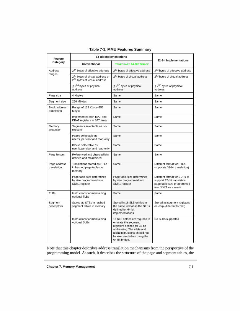
Chapter 7. Memory Management 7-3
Note that this chapter describes address translation mechanisms from the perspective of theprogramming model. As such, it describes the structure of the page and segment tables, the
Table 7-1. MMU Features Summary
Feature Category
64-Bit Implementations32-Bit Implementations
Conventional TEMPORARY 64-BIT BRIDGE
Address ranges
264 bytes of effective address 232 bytes of effective address 232 bytes of effective address
280 bytes of virtual address or264 bytes of virtual address
252 bytes of virtual address 252 bytes of virtual address
< 264 bytes of physical address
< 232 bytes of physical address
< 232 bytes of physical address
Page size 4 Kbytes Same Same
Segment size 256 Mbytes Same Same
Block address translation
Range of 128 Kbyte–256 Mbyte
Same Same
Implemented with IBAT and DBAT registers in BAT array
Same Same
Memory protection
Segments selectable as no-execute
Same Same
Pages selectable as user/supervisor and read-only
Same Same
Blocks selectable as user/supervisor and read-only
Same Same
Page history Referenced and changed bits defined and maintained
Same Same
Page address translation
Translations stored as PTEs in hashed page tables in memory
Same Different format for PTEs (supports 32-bit translation)
Page table size determined by size programmed into SDR1 register
Page table size determined by size programmed into SDR1 register
Different format for SDR1 to support 32-bit translation; page table size programmed into SDR1 as a mask
TLBs Instructions for maintaining optional TLBs
Same Same
Segment descriptors
Stored as STEs in hashed segment tables in memory
Stored in 16 SLB entries in the same format as the STEs defined for 64-bit implementations.
Stored as segment registers on-chip (different format)
Instructions for maintaining optional SLBs
16 SLB entries are required to emulate the segment registers defined for 32-bit addressing. The slbie and slbia instructions should not be executed when using the 64-bit bridge.
No SLBs supported

7-4 PowerPC Microprocessor Family: The Programming Environments, Rev. 1
MMU conditions that cause exceptions, the instructions provided for programming theMMU, and the MMU registers. The hardware implementation details of a particular MMU(including whether the hardware automatically performs a page table search in memory)are not contained in the architectural definition of PowerPC processors and are invisible tothe PowerPC programming model; therefore, they are not described in this document. Inthe case that some of the OEA model is implemented with some software assist mechanism,this software should be contained in the area of memory reserved for implementation-specific use and should not be visible to the operating system.
7.2 MMU OverviewThe PowerPC MMU and exception models support demand-paged virtual memory. Virtualmemory management permits execution of programs larger than the size of physicalmemory; the term demand paged implies that individual pages are loaded into physicalmemory from backing storage only as they are accessed by an executing program.
TEMPORARY 64-BIT BRIDGE
In addition to the features described above, the OEA provides optional features thatfacilitate the migration of operating systems from 32-bit processor designs to 64-bitprocessors. These features, which can be implemented in part or in whole, include thefollowing:
• Support for several 32-bit instructions that are otherwise defined as illegal in 64-bit processors. These include the following—mtsr, mtsrin, mfsr, mfsrin.
• Additional instructions, mtsrd and mtsrdin, that allow software to associate effective segments 0–15 with any of virtual segments 0–(252 – 1) without otherwise affecting the segment table. These instructions move 64 bits from a specified GPR to a selected SLB entry.
• The rfi and mtmsr instructions, which are otherwise illegal in the 64-bit architecture may optionally be implemented in 64-bit implementations.
• The bridge defines the following additional optional bits:
— ASR[V] (bit 63) may be implemented to indicate whether ASR[STABORG] holds a valid physical base address for the segment table.
— MSR[ISF] (bit 2) is defined as an optional bit that can be used to control the mode (64-bit or 32-bit) that is entered when an exception is taken. If the bit is implemented, it should have the properties described in Section 7.9.1, “ISF Bit of the Machine State Register.” Otherwise, it is treated as reserved, except that ISF is assumed to be set for exception processing.
To determine whether a processor implements any or all of the bridge features, consult theuser’s manual for that processor.
Chapter 7. Memory Management 7-5
The memory management model includes the concept of a virtual address that is not onlylarger than that of the maximum physical memory allowed but a virtual address space thatis also larger than the effective address space. Effective addresses generated by 64-bitimplementations are 64 bits wide; those generated by 32-bit implementations are 32 bitswide. In the address translation process, the processor converts an effective address to an80-bit (or 64-bit) virtual address in 64-bit implementations, or to a 52-bit virtual address in32-bit implementations, as per the information in the selected descriptor. Then the addressis translated back to a physical address the size (or less) of the effective address.
64-bit implementations have the option of supporting either an 80-bit or a 64-bit virtualaddress range. The remainder of this chapter describes the virtual address for 64-bitprocessors as consisting of 80 bits. For implementations that support the 64-bit virtualaddress range, the high-order 16 bits of the 80-bit virtual address are assumed to be zero.
Note that in the cases that 64-bit (or 32-bit) implementations support a physical addressrange that is smaller than 64 bits (or 32 bits), the higher-order bits of the effective addressmay be ignored in the address translation process. The remainder of this chapter assumesthat implementations support the maximum physical address range.
The operating system manages the system’s physical memory resources. Consequently, theoperating system initializes the MMU registers (segment registers or address space register(ASR), BAT registers, and SDR1 register) and sets up page tables (and segment tables for64-bit implementations) in memory appropriately. The MMU then assists the operatingsystem by managing page status and optionally caching the recently-used addresstranslation information on-chip for quick access.
Effective address spaces are divided into 256-Mbyte regions called segments or into otherlarge regions called blocks (128 Kbyte–256 Mbyte). Segments that correspond to memory-mapped areas can be further subdivided into 4-Kbyte pages. For each block or page, theoperating system creates an address descriptor (page table entry (PTE) or BAT array entry);the MMU then uses these descriptors to generate the physical address, the protectioninformation, and other access control information each time an address within the block orpage is accessed. Address descriptors for pages reside in tables (as PTEs) in physicalmemory; for faster accesses, the MMU often caches on-chip copies of recently-used PTEsin an on-chip TLB. The MMU keeps the block information on-chip in the BAT array(comprised of the BAT registers).
This section provides an overview of the high-level organization and operational conceptsof the MMU in PowerPC processors, and a summary of all MMU control registers. Formore information about the MSR, see Section 2.3.1, “Machine State Register (MSR).”Section 7.4.3, “BAT Register Implementation of BAT Array,” describes the BAT registers,Section 7.5.2.1, “Segment Descriptor Definitions,” describes the segment registers,Section 7.6.1.1, “SDR1 Register Definitions,” describes the SDR1, and Section 7.7.1.1,“Address Space Register (ASR),” describes the ASR.
7-6 PowerPC Microprocessor Family: The Programming Environments, Rev. 1
7.2.1 Memory AddressingA program references memory using the effective (logical) address computed by theprocessor when it executes a load, store, branch, or cache instruction, and when it fetchesthe next instruction. The effective address is translated to a physical address according tothe procedures described throughout this chapter. The memory subsystem uses the physicaladdress for the access.
7.2.1.1 Effective Addresses in 32-Bit ModeIn addition to the 64-and 32-bit memory management models defined by the OEA, thePowerPC architecture also defines a 32-bit mode of operation for 64-bit implementations.In this 32-bit mode (MSR[SF] = 0), the 64-bit effective address is first calculated as usual,and then the high-order 32 bits of the EA are treated as zero for the purposes of addressingmemory. This occurs for both instruction and data accesses, and occurs independently fromthe setting of the MSR[IR] and MSR[DR] bits that enable instruction and data addresstranslation, respectively. The truncation of the EA is the only way in which memoryaccesses are affected by the 32-bit mode of operation.
For a complete discussion of effective address calculation, see Section 4.1.4.2, “EffectiveAddress Calculation.”
7.2.1.2 Predefined Physical Memory LocationsThere are four areas of the physical memory map that have predefined uses. The first 256bytes of physical memory (or if MSR[IP] = 1, the first 256 bytes of memory located atphysical address 0xFFF0_0000 in 32-bit implementations and 0x0000_0000_FFF0_0000in 64-bit implementations) are assigned for arbitrary use by the operating system. The restof that first page of physical memory defined by the vector base address (determined byMSR[IP]) is either used for exception vectors, or reserved for future exception vectors. Thethird predefined area of memory consists of the second and third physical pages of thememory map, which are used for implementation-specific purposes. In someimplementations, the second and third pages located at physical address 0xFFF0_1000 in32-bit implementations and 0x0000_0000_FFF0_1000 in 64-bit implementations whenMSR[IP] = 1 are also used for implementation-specific purposes. Fourthly, the systemsoftware defines the locations in physical memory that contain the page address translationtables (and segment descriptor tables, in 64-bit implementations). These predefined
TEMPORARY 64-BIT BRIDGE
Some 64-bit processors implement optional features that simplify the conversion of anoperating system from the 32-bit to the 64-bit portion of the architecture. Thisarchitecturally-defined bridge allows an operating system to use 16 on-chip SLB entries inthe same manner that 32-bit implementations use the segment registers, which areotherwise not supported in the 64-bit architecture. These bridge features are available ifthe ASR[V] bit is implemented, and they are enabled when both ASR[V] and MSR[SF]are cleared.

Chapter 7. Memory Management 7-7
memory areas are summarized in Table 7-2 in terms of the variable ‘Base’ and Table 7-3decodes the actual value of ‘Base’. Refer to Chapter 6, “Exceptions,” for more detailedinformation on the assignment of the exception vector offsets.
7.2.2 MMU OrganizationFigure 7-1 shows the conceptual organization of the MMU in a 64-bit implementation; notethat it does not describe the specific hardware used to implement the memory managementfunction for a particular processor, and other hardware features (invisible to the systemsoftware) not depicted in the figure may be implemented. For example, the memorymanagement function can be implemented with parallel MMUs that translate addresses forinstruction and data accesses independently.
The instruction addresses shown in the figure are generated by the processor for sequentialinstruction fetches and addresses that correspond to a change of program flow. Memoryaddresses are generated by load and store instructions, by cache instructions, and by theoptional external control instructions.
As shown in Figure 7-1, after an address is generated, the higher-order bits of the effectiveaddress, EA0–EA51 (or a smaller set of address bits, EA0–EAn, in the cases of blocks), aretranslated into physical address bits PA0–PA51. The lower-order address bits, A52–A63 areuntranslated and therefore identical for both effective and physical addresses. Aftertranslating the address, the MMU passes the resulting 64-bit physical address to thememory subsystem.
Table 7-2. Predefined Physical Memory Locations
Memory Area Physical Address Range Predefined Use
1 Base || 0x0_0000–Base || 0x0_00FF Operating system
2 Base || 0x0_0100–Base || 0x0_0FFF Exception vectors
3 Base || 0x0_1000–Base || 0x0_2FFF Implementation-specific1
4 Software-specified—contiguous sequence of physical pages
Page table
Software-specified—single physical page Segment table (64-bit implementations only)
1Only valid for MSR[IP] = 1 on some implementations
Table 7-3. Value of Base for Predefined Memory Use
MSR[IP] Value of Base
0 Base = 0x000 for 32-bit implementationsBase = 0x0000_0000_000 for 64-bit implementations
1 Base = 0xFFF for 32-bit implementationsBase = 0x0000_0000_FFF for 64-bit implementations
7-8 PowerPC Microprocessor Family: The Programming Environments, Rev. 1
In addition to the higher-order address bits, the MMU automatically keeps an indicator ofwhether each access was generated as an instruction or data access and a supervisor/userindicator that reflects the state of the MSR[PR] bit when the effective address wasgenerated. In addition, for data accesses, there is an indicator of whether the access is for aload or a store operation. This information is then used by the MMU to appropriately directthe address translation and to enforce the protection hierarchy programmed by theoperating system. See Section 2.3.1, “Machine State Register (MSR),” for moreinformation about the MSR.

Chapter 7. Memory Management 7-9
Figure 7-1. MMU Conceptual Block Diagram—64-Bit Implementations
EA
0–E
A51
MMU(64 Bit)
A52–A63EA
0–E
A51
IBAT0UIBAT0L
•
•
IBAT3UIBAT3L
SPR25
PA0–PA63
+
EA0–EA46
Segment Table Search Logic
DataAccesses
InstructionAccesses
X
A52
–A63
EA0–EA46 DBAT0UDBAT0L
•
•
DBAT3UDBAT3L
X
PA47–PA51
EA47–EA51
+
EA
36–E
A51
SDR1
ASR
Upper 52 bits of virtual address
EA0–EA51
EA0–EA35
On-ChipSLBs
PA0–PA46
X
X
PA0–PA51
BAT Hit ←
EA47–EA51
SPR280
On-ChipTLBs
Optional
Page Table Search Logic
7-10 PowerPC Microprocessor Family: The Programming Environments, Rev. 1
As shown in Figure 7-1, processors optionally implement on-chip translation lookasidebuffers (TLBs) and optionally support the automatic search of the page tables for page tableentries (PTEs).
In 64-bit implementations, the address space register (ASR) defines the physical address ofthe base of the segment table in memory. The segment table entries (STEs) contain thesegment descriptors, which define the virtual address for the segment. Some 64-bitimplementations may have dedicated hardware to search for STEs in memory, and copiesof STEs may be cached on-chip in segment lookaside buffers (SLBs) for quicker access.
Figure 7-2 shows a conceptual block diagram of the MMU in a 32-bit implementation. The32-bit MMU implementation differs from the 64-bit implementation in that after an addressis generated, the higher-order bits of the effective address, EA0–EA19 (or a smaller set ofaddress bits, EA0–EAn, in the cases of blocks), are translated into physical address bitsPA0–PA19. The lower-order address bits, A20–A31 are untranslated and therefore identicalfor both effective and physical addresses. After translating the address, the MMU passes theresulting 32-bit physical address to the memory subsystem.
Also, whereas 64-bit implementations use the ASR and a segment table to generate the80-bit virtual address, 32-bit implementations use the 16 segment registers to generate the52-bit virtual address.
TEMPORARY 64-BIT BRIDGE
Processors that implement the 64-bit bridge implement segment descriptors as a table of16 segment table entries.

Chapter 7. Memory Management 7-11
Figure 7-2. MMU Conceptual Block Diagram—32-Bit Implementations
MMU(32 Bit)
A20–A31
X
EA
0–E
A19
EA
0–E
A19
EA0–EA3
0
15
Segment Registers...
PA0–PA31
EA0–EA14
EA0–EA14
EA4–EA19
On-ChipTLBs
DataAccesses
InstructionAccesses
A20
–A31
SPR25SDR1
+
X
DBAT0UDBAT0L
•
•
DBAT3UDBAT3L
PA15–PA19
X
←
XEA15–EA19
Upper 24 bits of virtual address
EA15–EA19
PA0–PA14
PA0–PA19
BAT Hit
IBAT0UIBAT0L
•
•
IBAT3UIBAT3L
+
Page Table Search Logic
Optional

7-12 PowerPC Microprocessor Family: The Programming Environments, Rev. 1
7.2.3 Address Translation MechanismsPowerPC processors support the following three types of address translation:
• Page address translation—translates the page frame address for a 4-Kbyte page size
• Block address translation—translates the block number for blocks that range in size from 128 Kbyte to 256 Mbyte
• Real addressing mode address translation—when address translation is disabled, the physical address is identical to the effective address.
In addition, earlier processors implement a direct-store facility that is used to generatedirect-store interface accesses on the external bus. Note that this facility is not optimizedfor performance, was present for compatibility with POWER devices, and is being phasedout of the architecture. Future devices are not likely to support it; software should notdepend on its effects and new software should not use it.
Figure 7-3 shows the address translation mechanisms provided by the MMU. The segmentdescriptors shown in the figure control both the page and direct-store segment addresstranslation mechanisms. When an access uses the page or direct-store segment addresstranslation, the appropriate segment descriptor is required. In 64-bit implementations, thesegment descriptor is located via a search of the segment table in memory for theappropriate segment table entry (STE). In 32-bit implementations, one of the 16 on-chipsegment registers (which contain segment descriptors) is selected by the highest-ordereffective address bits.
A control bit in the corresponding segment descriptor then determines if the access is tomemory (memory-mapped) or to a direct-store segment. Note that the direct-store interfaceis present to allow certain older I/O devices to use this interface. When an access isdetermined to be to the direct-store interface space, the implementation invokes anelaborate hardware protocol for communication with these devices. The direct-storeinterface protocol is not optimized for performance, and therefore, its use is discouraged.The most efficient method for accessing I/O is by memory-mapping the I/O areas.
For memory accesses translated by a segment descriptor, the interim virtual address isgenerated using the information in the segment descriptor. Page address translationcorresponds to the conversion of this virtual address into the 64-bit (or 32-bit) physicaladdress used by the memory subsystem. In some cases, the physical address for the pageresides in an on-chip TLB and is available for quick access. However, if the page addresstranslation misses in a TLB, the MMU searches the page table in memory (using the virtualaddress information and a hashing function) to locate the required physical address. Some
TEMPORARY 64-BIT BRIDGE
Processors that implement the 64-bit bridge divide the 32-bit address space into sixteen256-Mbyte segments defined by a table of 16 STEs maintained in 16 SLB entries.

Chapter 7. Memory Management 7-13
implementations may have dedicated hardware to perform the page table searchautomatically, while others may define an exception handler routine that searches the pagetable with software.
Block address translation occurs in parallel with page (and direct-store segment) addresstranslation and is similar to page address translation, except that there are fewer upper-ordereffective address bits to be translated into physical address bits (more lower-order addressbits (at least 17) are untranslated to form the offset into a block). Also, instead of segmentdescriptors and a page table, block address translations use the on-chip BAT registers as aBAT array. If an effective address matches the corresponding field of a BAT register, theinformation in the BAT register is used to generate the physical address; in this case, theresults of the page translation (occurring in parallel) are ignored. Note that a matching BATarray entry takes precedence over a translation provided by the segment descriptor in allcases (even if the segment is a direct-store segment).

7-14 PowerPC Microprocessor Family: The Programming Environments, Rev. 1
Figure 7-3. Address Translation Types—64-Bit Implementations
TEMPORARY 64-BIT BRIDGE
Note that Figure 7-3 shows address sizes for a 64-bit processor operating in 64-bit mode.If the 64-bit bridge is enabled (ASR[V] is cleared), only the 32-bit address space isavailable and only 52 bits of the virtual address are used. However, the bridge supportscross-memory operations that permit an operating system to establish addressability to anaddress space, to copy data to it from another address space, and then to destroy the newaddressability, without altering the segment table. For more information, see Section 7.9.5,“Segment Register Instructions Defined Exclusively for the 64-Bit Bridge.”
(T = 1) (T = 0)
0 63Effective Address
0 79Virtual Address
Segment Descriptor Located
Match with BAT Registers
0 63Physical Address
0 63 Implementation-Dependent
0 63Physical Address
0 63Physical Address
Look Up in Page Table
Address Translation Disabled
Page Address
Direct-Store Segment Translation
(see Section 7.8)
Block Address Translation
(see Section 7.4)
(MSR[IR] = 0, or MSR[DR] = 0)
Real Addressing Mode Effective Address = Physical Address
(see Section 7.3)

Chapter 7. Memory Management 7-15
Direct-store address translation is used when the optional direct-store translation control bit(T bit) in the corresponding segment descriptor is set (being phased out of the architecture).In this case, the remaining information in the segment descriptor is interpreted as identifierinformation that is used with the remaining effective address bits to generate the protocolused in a direct-store interface access on the external interface; additionally, no TLB lookupor page table search is performed.
Real addressing mode address translation occurs when address translation is disabled; inthis case, the physical address generated is identical to the effective address. Instruction anddata address translation is enabled with the MSR[IR] and MSR[DR] bits, respectively.Thus, when the processor generates an access, and the corresponding address translationenable bit in MSR (MSR[IR] for instruction accesses and MSR[DR] for data accesses) iscleared, the resulting physical address is identical to the effective address and all othertranslation mechanisms are ignored. See Section 7.2.6.1, “Real Addressing Mode andBlock Address Translation Selection,” for more information.
7.2.4 Memory Protection FacilitiesIn addition to the translation of effective addresses to physical addresses, the MMUprovides access protection of supervisor areas from user access and can designate areas ofmemory as read-only as well as no-execute. Table 7-4 shows the eight protection optionssupported by the MMU for pages.
Table 7-4. Access Protection Options for Pages
OptionUser Read
User Write
Supervisor ReadSupervisor
WriteI-Fetch Data I-Fetch Data
Supervisor-only — — — √ √ √
Supervisor-only-no-execute — — — — √ √
Supervisor-write-only √ √ — √ √ √
Supervisor-write-only-no-execute — √ — — √ √
Both user/supervisor √ √ √ √ √ √
Both user/supervisor-no-execute — √ √ — √ √
Both read-only √ √ — √ √ —
Both read-only-no-execute — √ — — √ —
√ Access permitted — Protection violation

7-16 PowerPC Microprocessor Family: The Programming Environments, Rev. 1
The operating system programs whether or not instruction fetches are allowed from an areaof memory with the no-execute option provided in the segment descriptor. Each of theremaining options is enforced based on a combination of information in the segmentdescriptor and the page table entry. Thus, the supervisor-only option allows only read andwrite operations generated while the processor is operating in supervisor mode(corresponding to MSR[PR] = 0) to access the page. User accesses that map into asupervisor-only page cause an exception to be taken.
Note that independently of the protection mechanisms, care must be taken when writing toinstruction areas as coherency must be maintained with on-chip copies of instructions thatmay have been prefetched into a queue or an instruction cache. Refer to Section 5.1.5.2,“Instruction Cache Instructions,” for more information on coherency within instructionareas.
As shown in the table, the supervisor-write-only option allows both user and supervisoraccesses to read from the page, but only supervisor programs can write to that area. Thereis also an option that allows both supervisor and user programs read and write access (bothuser/supervisor option), and finally, there is an option to designate a page as read-only, bothfor user and supervisor programs (both read-only option).
For areas of memory that are translated by the block address translation mechanism, theprotection options are similar, except that blocks are translated by separate mechanisms forinstruction and data, blocks do not have a no-execute option, and blocks can be designatedas enabled for user and supervisor accesses independently. Therefore, a block can bedesignated as supervisor-only, for example, but this block can be programmed such that alluser accesses simply ignore the block translation, rather than take an exception in the caseof a match. This allows a flexible way for supervisor and user programs to use overlappingeffective address space areas that map to unique physical address areas (without exceptionsoccurring).
For direct-store segments, the MMU calculates a key bit based on the protection valuesprogrammed in the segment descriptor and the specific user/supervisor and read/writeinformation for the particular access. However, this bit is merely passed on to the systeminterface to be transmitted in the context of the direct-store interface protocol. The MMUdoes not itself enforce any protection or cause any exception based on the state of the keybit for these accesses. The I/O controller device or other external hardware can optionallyuse this bit to enforce any protection required. Note that the direct-store facility is beingphased out of the architecture and future devices are not likely to implement it.
Finally, a facility defined in the VEA and OEA allows pages or blocks to be designated asguarded, preventing out-of-order accesses that may cause undesired side effects. Forexample, areas of the memory map that are used to control I/O devices can be marked asguarded so that accesses (for example, instruction prefetches) do not occur unless they areexplicitly required by the program. Refer to Section 5.2.1.5.3, “Out-of-Order Accesses toGuarded Memory,” for a complete description of how accesses to guarded memory arerestricted.
Chapter 7. Memory Management 7-17
7.2.5 Page History InformationThe MMU of PowerPC processors also defines referenced (R) and changed (C) bits in thepage address translation mechanism that can be used as history information relevant to thevirtual page. This information can then be used by the operating system to determine whichareas of memory to write back to disk when new pages must be allocated in main memory.While these bits are initially programmed by the operating system into the page table, thearchitecture specifies that the R and C bits are maintained by the processor and theprocessor updates these bits when required.
7.2.6 General Flow of MMU Address TranslationThe following sections describe the general flow used by PowerPC processors to translateeffective addresses to virtual and then physical addresses. Note that although there arereferences to the concept of an on-chip TLB and SLB, these entities may not be present ina particular hardware implementation for performance enhancement (and a particularimplementation may have one or more TLBs and SLBs). Thus, they are shown here asoptional and only the software ramifications of the existence of a TLB or SLB arediscussed.
7.2.6.1 Real Addressing Mode and Block Address Translation Selection
When an instruction or data access is generated and the corresponding instruction or datatranslation is disabled (MSR[IR] = 0 or MSR[DR] = 0), real addressing mode translation isused (physical address equals effective address) and the access continues to the memorysubsystem as described in Section 7.3, “Real Addressing Mode.”
Figure 7-4 shows the flow used by the MMU in determining whether to select realaddressing mode or block address translation or to use the segment descriptor to selecteither direct-store or page address translation.

7-18 PowerPC Microprocessor Family: The Programming Environments, Rev. 1
Figure 7-4. General Flow of Address Translation (Real Addressing Mode and Block)
Note that if the BAT array search results in a hit, the access is qualified with the appropriateprotection bits. If the access is determined to be protected (not allowed), an exception (ISIor DSI exception) is generated.
7.2.6.2 Page and Direct-Store Address Translation Selection If address translation is enabled (real addressing mode translation not selected) and theeffective address information does not match with a BAT array entry, then the segmentdescriptor must be located. Once the segment descriptor is located, the T bit in the segmentdescriptor selects whether the translation is to a page or to a direct-store segment as shownin Figure 7-5. In addition, Figure 7-5 also shows the way in which the no-executeprotection is enforced; if the N bit in the segment descriptor is set and the access is aninstruction fetch, the access is faulted.
BAT ArrayMiss
BAT ArrayHit
Access Protected
Access Permitted
Perform Address Translation with Segment Descriptor
Access Faulted Translate Address
D-accessI-access
DataTranslation Disabled
(MSR[DR] = 0)
InstructionTranslation Disabled
(MSR[IR] = 0)
Effective AddressGenerated
Continue Accessto Memory Subsystem
InstructionTranslation Enabled
(MSR[IR] = 1)
DataTranslation Enabled
(MSR[DR] = 1)
(See Figure 7-16)
(see Figure 7-5)
Perform Real Addressing Mode
TranslationCompare Address with Instruction or Data BAT Array (as appropriate)
Perform Real Addressing Mode
Translation
(See Figure 7-8)

Chapter 7. Memory Management 7-19
Figure 7-5. General Flow of Page and Direct-Store Address Translation
Access Faulted
Access Faulted
Access Protected
Access Permitted
Continue Accessto Memory Subsystem
Translate Address
Perform Direct-Store Segment Translation
Direct-Store Segment Address
(T = 1)*
Page Address Translation
(T = 0)
Load TLB Entry
TLBMiss
Generate 80-Bit(or 52-Bit) Virtual
Address from Segment Descriptor
Compare Virtual Address with TLB
Entries
Locate Segment Descriptor
Address Translation with Segment Descriptor
(See Figure 7-6)
(See Figure 7-49)
(See Figure 7-24)
(See Figure 7-39)
I-Fetch with N bit set in Segment Descriptor
(no-execute)
TLBHit
otherwise
Check T bit in Segment Descriptor
Perform Page Table Search Operation
PTE FoundPTE Not Found
Notes:* Not allowed for instruction accesses
(causes ISI exception)
Implementation-specific

7-20 PowerPC Microprocessor Family: The Programming Environments, Rev. 1
The segment descriptor is contained in different constructs for 64- and 32-bitimplementations as shown in Figure 7-6. For 64-bit implementations, the segmentdescriptor for each access is located in an STE that resides in a segment table in memory.The base address of this segment table is specified in the address space register (ASR) andthe entries of the table are located by using a hashing function. Although it is notarchitecturally required, hardware implementations may have one or more on-chip SLBsthat keep recently-used STEs for quick access.
For 32-bit implementations, the segment descriptor for an access is contained in one of 16on-chip segment registers; effective address bits EA0–EA3 select one of the 16 segmentregisters.
TEMPORARY 64-BIT BRIDGE
Processors that implement the 64-bit bridge maintain segment descriptors on-chip byemulating segment tables in 16 SLB entries. As shown in Figure 7-6, this feature is enabledby clearing the optional ASR[V] bit. This indicates that any value in the STABORG isinvalid and that segment table hashing is not implemented.

Chapter 7. Memory Management 7-21
Figure 7-6. Location of Segment Descriptors
7.2.6.2.1 Selection of Page Address TranslationIf the T bit in the corresponding segment descriptor is 0, page address translation isselected. The information in the segment descriptor is then used to generate the 80-bit (or52-bit) virtual address. The virtual address is then used to identify the page addresstranslation information (stored as page table entries (PTEs) in a page table in memory).Once again, although the architecture does not require the existence of a TLB, one or more
Access Faulted
Use EA0–EA3 to select one of 16 on-
chip segment registers
Locate STE(64-bit implementation)
SLB Miss SLB Hit
Perform Segment Table Search Operation
Use ASR
STE Not Found STE Found
Load SLB Entry
Check T bit inSegment Descriptor
Locate Segment Descriptor
Use EA0–EA3 to select one of 16 segment registers mapped to SLB entries
TEMPORARY 64-BIT BRIDGE
Locate emulated SR(ASR[V] = 0)
Locate Segment Register(32-bit implementation)
Compare EA with SLB entries
Implementation-specificNote:

7-22 PowerPC Microprocessor Family: The Programming Environments, Rev. 1
TLBs may be implemented in the hardware to store copies of recently-used PTEs on-chipfor increased performance.
If an access hits in the TLB, the page translation occurs and the physical address bits areforwarded to the memory subsystem. If the translation is not found in the TLB, the MMUrequires a search of the page table. The hardware of some implementations may performthe table search automatically, while others may trap to an exception handler for the systemsoftware to perform the page table search. If the translation is found, a new TLB entry iscreated and the page translation is once again attempted. This time, the TLB is guaranteedto hit. Once the PTE is located, the access is qualified with the appropriate protection bits.If the access is determined to be protected (not allowed), an exception (ISI or DSIexception) is generated.
If the PTE is not found by the table search operation, an ISI or DSI exception is generated.
7.2.6.2.2 Selection of Direct-Store Address Translation When the segment descriptor has the T bit set, the access is considered a direct-store accessand the direct-store interface protocol of the external interface is used to perform the access.The selection of address translation type differs for instruction and data accesses only inthat instruction accesses are not allowed from direct-store segments; attempting to fetch aninstruction from a direct-store segment causes an ISI exception.
Note that this facility is not optimized for performance, was present for compatibility withPOWER devices, and is being phased out of the architecture. Future devices are not likelyto support it; software should not depend on its effects and new software should not use it.See Section 7.8, “Direct-Store Segment Address Translation,” for more detailedinformation about the translation of addresses in direct-store segments in those processorsthat implement this.
7.2.7 MMU Exceptions SummaryIn order to complete any memory access, the effective address must be translated to aphysical address. A translation exception condition occurs if this translation fails for one ofthe following reasons:
• There is no valid entry in the page table for the page specified by the effective address (and segment descriptor) and there is no valid BAT translation.
• There is no valid segment descriptor and there is no valid BAT translation.
• An address translation is found but the access is not allowed by the memory protection mechanism.
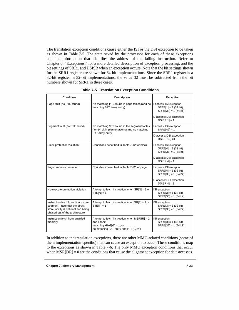
Chapter 7. Memory Management 7-23
The translation exception conditions cause either the ISI or the DSI exception to be takenas shown in Table 7-5. The state saved by the processor for each of these exceptionscontains information that identifies the address of the failing instruction. Refer toChapter 6, “Exceptions,” for a more detailed description of exception processing, and thebit settings of SRR1 and DSISR when an exception occurs. Note that the bit settings shownfor the SRR1 register are shown for 64-bit implementations. Since the SRR1 register is a32-bit register in 32-bit implementations, the value 32 must be subtracted from the bitnumbers shown for SRR1 in these cases.
In addition to the translation exceptions, there are other MMU-related conditions (some ofthem implementation-specific) that can cause an exception to occur. These conditions mapto the exceptions as shown in Table 7-6. The only MMU exception conditions that occurwhen MSR[DR] = 0 are the conditions that cause the alignment exception for data accesses.
Table 7-5. Translation Exception Conditions
Condition Description Exception
Page fault (no PTE found) No matching PTE found in page tables (and no matching BAT array entry)
I access: ISI exceptionSRR1[1] = 1 (32 bit)SRR1[33] = 1 (64 bit)
D access: DSI exceptionDSISR[1] = 1
Segment fault (no STE found) No matching STE found in the segment tables (for 64-bit implementations) and no matching BAT array entry
I access: ISI exceptionSRR1[42] = 1
D access: DSI exceptionDSISR[10] =1
Block protection violation Conditions described in Table 7-12 for block I access: ISI exceptionSRR1[4] = 1 (32 bit)SRR1[36] = 1 (64 bit)
D access: DSI exceptionDSISR[4] = 1
Page protection violation Conditions described in Table 7-22 for page I access: ISI exceptionSRR1[4] = 1 (32 bit)SRR1[36] = 1 (64 bit)
D access: DSI exceptionDSISR[4] = 1
No-execute protection violation Attempt to fetch instruction when SR[N] = 1 or STE[N] = 1
ISI exceptionSRR1[3] = 1 (32 bit)SRR1[35] = 1 (64 bit)
Instruction fetch from direct-store segment—note that the direct-store facility is optional and being phased out of the architecture.
Attempt to fetch instruction when SR[T] = 1 or STE[T] = 1
ISI exceptionSRR1[3] = 1 (32 bit)SRR1[35] = 1 (64 bit)
Instruction fetch from guarded memory
Attempt to fetch instruction when MSR[IR] = 1 and either: matching xBAT[G] = 1, orno matching BAT entry and PTE[G] = 1
ISI exceptionSRR1[3] = 1 (32 bit)SRR1[35] = 1 (64 bit)

7-24 PowerPC Microprocessor Family: The Programming Environments, Rev. 1
For more detailed information about the conditions that cause the alignment exception (inparticular for string/multiple instructions), see Section 6.4.6, “Alignment Exception(0x00600).” Refer to Chapter 6, “Exceptions,” for a complete description of the SRR1 andDSISR bit settings for these exceptions.
7.2.8 MMU Instructions and Register SummaryThe MMU instructions and registers provide the operating system with the ability to set upthe segment descriptors. Additionally, the operating system has the resources to set up theblock address translation areas and the page tables in memory.
Table 7-6. Other MMU Exception Conditions
Condition Description Exception
dcbz with W = 1 or I = 1 (may cause exception or operation may be performed to memory)
dcbz instruction to write-through or cache-inhibited segment or block
Alignment exception (implementation-dependent)
ldarx, stdcx., lwarx, or stwcx. with W = 1 (may cause exception or execute correctly)
Reservation instruction to write-through segment or block
DSI exception (implementation-dependent)
DSISR[5] = 1
ldarx, stdcx., lwarx, stwcx., eciwx, or ecowx instruction to direct-store segment (may cause exception or may produce boundedly-undefined results)—note that the direct-store facility is optional and being phased out of the architecture
Reservation instruction or external control instruction when SR[T] = 1 or STE[T] = 1
DSI exception (implementation-dependent)
DSISR[5] = 1
Floating-point load or store to direct-store segment (may cause exception or instruction may execute correctly)—note that the direct-store facility is optional and being phased out of the architecture
Floating-point memory access when SR[T] = 1 or STE[T] = 1
Alignment exception (implementation-dependent)
Load or store operation that causes a direct-store error—note that the direct-store facility is optional and being phased out of the architecture
Direct-store interface protocol signalled with an error condition
DSI exceptionDSISR[0] = 1
eciwx or ecowx attempted when external control facility disabled
eciwx or ecowx attempted with EAR[E] = 0
DSI exceptionDSISR[11] = 1
lmw, stmw, lswi, lswx, stswi, or stswx instruction attempted in little-endian mode
lmw, stmw, lswi, lswx, stswi, or stswx instruction attempted while MSR[LE] = 1
Alignment exception
Operand misalignment Translation enabled and operand is misaligned as described in Chapter 6, “Exceptions.”
Alignment exception (some of these cases are implementation-dependent)
Chapter 7. Memory Management 7-25
Note that because the implementation of TLBs and SLBs is optional, the instructions thatrefer to these structures are also optional. However, as these structures serve as caches ofthe page table (and segment table, in the case of an SLB), there must be a software protocolfor maintaining coherency between these caches and the tables in memory wheneverchanges are made to the tables in memory. Therefore, the PowerPC OEA specifies that aprocessor implementing a TLB is guaranteed to have a means for doing the following:
• Invalidating an individual TLB entry• Invalidating the entire TLB
Similarly, a processor that implements an SLB is guaranteed to have a means for doing thefollowing:
• Invalidating an individual SLB entry (the architecture defines an optional slbie instruction for this purpose)
• Invalidating the entire SLB (the architecture defines an optional slbia instruction for this purpose)
When the tables in memory are changed, the operating system purges these caches of thecorresponding entries, allowing the translation caching mechanism to refetch from thetables when the corresponding entries are required.
A processor may implement one or more of the instructions described in this section tosupport table invalidation. Alternatively, an algorithm may be specified that performs oneof the functions listed above (a loop invalidating individual TLB entries may be used toinvalidate the entire TLB, for example), or different instructions may be provided.
A processor may also perform additional functions (not described here) as well as thosedescribed in the implementation of some of these instructions. For example, the tlbieinstruction may be implemented so as to purge all TLB entries in a congruence class (thatis, all TLB entries indexed by the specified EA which can include corresponding entries indata and instruction TLBs) or the entire TLB.
Note that if a processor does not implement an optional instruction it treats the instructionas a no-op or as an illegal instruction, depending on the implementation. Also, note that thesegment register and TLB concepts described here are conceptual; that is, a processor mayimplement parallel sets of segment registers (and even TLBs) for instructions and data.
TEMPORARY 64-BIT BRIDGE
Note that while the implementation of SLBs in 64-bit processors is optional, processorsthat implement the 64-bit bridge are required to implement at least 16 SLB entries toprovide a means of emulating the segment registers as they are defined in the 32-bitarchitecture. When the processor is using the 64-bit bridge, neither the slbie or slbiainstruction should be executed.

7-26 PowerPC Microprocessor Family: The Programming Environments, Rev. 1
Because the MMU specification for PowerPC processors is so flexible, it is recommendedthat the software that uses these instructions and registers be encapsulated into subroutinesto minimize the impact of migrating across the family of implementations.
Table 7-7 summarizes the PowerPC instructions that specifically control the MMU. Formore detailed information about the instructions, refer to Chapter 8, “Instruction Set.”
Table 7-8 summarizes the registers that the operating system uses to program the MMU.These registers are accessible to supervisor-level software only (supervisor level is referredto as privileged state in the architecture specification). These registers are described indetail in Chapter 2, “PowerPC Register Set.”
Table 7-7. Instruction Summary—Control MMU
Instruction Description
mtsr SR,rS Move to Segment RegisterSR[SR]← rS32-bit implementations and 64-bit bridge only
mtsrin rS,rB Move to Segment Register IndirectSR[rB[0–3]]←rS32-bit implementations and 64-bit bridge only
TEMPORARY 64-BIT BRIDGE
mtsrd SR,rS
Move to Segment Register Double WordSLB[SR]← rS64-bit bridge only
mtsrdin rS,rB Move to Segment Register Indirect Double Word SLB(rB[32-35]) ← (rS)64-bit bridge only
mfsr rD,SR Move from Segment RegisterrD←SR[SR]32-bit implementations and 64-bit bridge only
mfsrin rD,rB Move from Segment Register IndirectrD←SR[rB[0–3]] 32-bit implementations and 64-bit bridge only
tlbia(optional)
Translation Lookaside Buffer Invalidate AllFor all TLB entries, TLB[V]←0 Causes invalidation of TLB entries only for processor that executed the tlbia
tlbie rB(optional)
Translation Lookaside Buffer Invalidate EntryIf TLB hit (for effective address specified as rB), TLB[V]←0 Causes TLB invalidation of entry in all processors in system
tlbsync(optional)
Translation Lookaside Buffer SynchronizeEnsures that all tlbie instructions previously executed by the processor executing the tlbsync instruction have completed on all processors
slbia(optional)
Segment Table Lookaside Buffer Invalidate AllFor all SLB entries, SLB[V]←0 64-bit implementations only
slbie rB(optional)
Segment Table Lookaside Buffer Invalidate EntryIf SLB hit (for effective address specified as rB), SLB[V]←0 64-bit implementations only

Chapter 7. Memory Management 7-27
7.2.9 TLB Entry InvalidationOptionally, PowerPC processors implement TLB structures that store on-chip copies of thePTEs that are resident in physical memory. These processors have the ability to invalidateresident TLB entries through the use of the tlbie and tlbia instructions. Additionally, theseinstructions may also enable a TLB invalidate signalling mechanism in hardware so thatother processors also invalidate their resident copies of the matching PTE. See Chapter 8,“Instruction Set,” for detailed information about the tlbie and tlbia instructions.
7.3 Real Addressing ModeIf address translation is disabled (MSR[IR] = 0 or MSR[DR] = 0) for a particular access,the effective address is treated as the physical address and is passed directly to the memorysubsystem as a real addressing mode address translation. If an implementation has a smallerphysical address range than effective address range, the extra high-order bits of the effectiveaddress may be ignored in the generation of the physical address.
Section 2.3.18, “Synchronization Requirements for Special Registers and for LookasideBuffers,” describes the synchronization requirements for changes to MSR[IR] andMSR[DR].
The addresses for accesses that occur in real addressing mode bypass all memory protectionchecks as described in Section 7.4.4, “Block Memory Protection,” and Section 7.5.4, “PageMemory Protection” and do not cause the recording of referenced and changed information(described in Section 7.5.3, “Page History Recording”).
Table 7-8. MMU Registers
Register Description
Segment registers(SR0–SR15)
The sixteen 32-bit segment registers are present only in 32-bit implementations of the PowerPC architecture. Figure 7-20 shows the format of a segment register. The fields in the segment register are interpreted differently depending on the value of bit 0. The segment registers are accessed by the mtsr, mtsrin, mfsr, and mfsrin instructions.
BAT registers (IBAT0U–IBAT3U, IBAT0L–IBAT3L, DBAT0U–DBAT3U, and DBAT0L–DBAT3L)
There are 16 BAT registers, organized as four pairs of instruction BAT registers (IBAT0U–IBAT3U paired with IBAT0L–IBAT3L) and four pairs of data BAT registers (DBAT0U–DBAT3U paired with DBAT0L–DBAT3L). The BAT registers are defined as 32-bit registers in 32-bit implementations, and 64-bit registers in 64-bit implementations. These are special-purpose registers that are accessed by the mtspr and mfspr instructions.
SDR1 register The SDR1 register specifies the base and size of the page tables in memory. SDR1 is defined as a 64-bit register for 64-bit implementations and as a 32-bit register for 32-bit implementations. This is a special-purpose register that is accessed by the mtspr and mfspr instructions.
Address space register(ASR)
The 64-bit ASR specifies the physical address in memory of the segment table for 64-bit implementations. This is a special-purpose register that is accessed by the mtspr and mfspr instructions.
7-28 PowerPC Microprocessor Family: The Programming Environments, Rev. 1
For data accesses that use real addressing mode, the memory access mode bits (WIMG) areassumed to be 0b0011. That is, the cache is write-back and memory does not need to beupdated immediately (W = 0), caching is enabled (I = 0), data coherency is enforced withmemory, I/O, and other processors (caches) (M = 1, so data is global), and the memory isguarded. For instruction accesses in real addressing mode, the memory access mode bits(WIMG) are assumed to be either 0b0001 or 0b0011. That is, caching is enabled (I = 0) andthe memory is guarded. Additionally, coherency may or may not be enforced with memory,I/O, and other processors (caches) (M = 0 or 1, so data may or may not be consideredglobal). For a complete description of the WIMG bits, refer to Section 5.2.1,“Memory/Cache Access Attributes.”
Note that the attempted execution of the eciwx or ecowx instructions while MSR[DR] = 0causes boundedly-undefined results.
Whenever an exception occurs, the processor clears both the MSR[IR] and MSR[DR] bits.Therefore, at least at the beginning of all exception handlers (including reset), the processoroperates in real addressing mode for instruction and data accesses. If address translation isrequired for the exception handler code, the software must explicitly enable addresstranslation by accessing the MSR as described in Chapter 2, “PowerPC Register Set.”
Note that an attempt to access a physical address that is not physically present in the systemmay cause a machine check exception (or even a checkstop condition), depending on theresponse by the system for this case. Thus, care must be taken when generating addressesin real addressing mode. Note that this can also occur when translation is enabled and theASR or SDR1 registers set up the translation such that nonexistent memory is accessed. SeeSection 6.4.2, “Machine Check Exception (0x00200),” for more information on machinecheck exceptions.
7.4 Block Address TranslationThe block address translation (BAT) mechanism in the OEA provides a way to map rangesof effective addresses larger than a single page into contiguous areas of physical memory.Such areas can be used for data that is not subject to normal virtual memory handling(paging), such as a memory-mapped display buffer or an extremely large array of numericaldata.
The following sections describe the implementation of block address translation inPowerPC processors, including the block protection mechanism, followed by a blocktranslation summary with a detailed flow diagram.
TEMPORARY 64-BIT BRIDGE
Note that if ASR[V] = 0, a reference to a nonexistent address in the STABORG field doesnot cause a machine check exception.
Chapter 7. Memory Management 7-29
7.4.1 BAT Array OrganizationThe block address translation mechanism in PowerPC processors is implemented as asoftware-controlled BAT array. The BAT array maintains the address translationinformation for eight blocks of memory. The BAT array in PowerPC processors ismaintained by the system software and is implemented as a set of 16 special-purposeregisters (SPRs). Each block is defined by a pair of SPRs called upper and lower BATregisters that contain the effective and physical addresses for the block.
The BAT registers can be read from or written to by the mfspr and mtspr instructions;access to the BAT registers is privileged. Section 7.4.3, “BAT Register Implementation ofBAT Array,” gives more information about the BAT registers. Note that the BAT arrayentries are completely ignored for TLB invalidate operations detected in hardware and inthe execution of the tlbie or tlbia instruction.
Figure 7-7 shows the organization of the BAT array in a 64-bit implementation. Four pairsof BAT registers are provided for translating instruction addresses and four pairs of BATregisters are used for translating data addresses. These eight pairs of BAT registerscomprise two four-entry fully-associative BAT arrays (each BAT array entry correspondsto a pair of BAT registers). The BAT array is fully-associative in that any address can residein any BAT. In addition, the effective address field of all four corresponding entries(instruction or data) is simultaneously compared with the effective address of the access tocheck for a match.
The BAT array organization for 32-bit implementations is the same as that shown inFigure 7-7 except that the effective address field to be compared with the BEPI field (blockeffective page index) in the upper BAT register is EA0–EA14 instead of EA0–EA46.
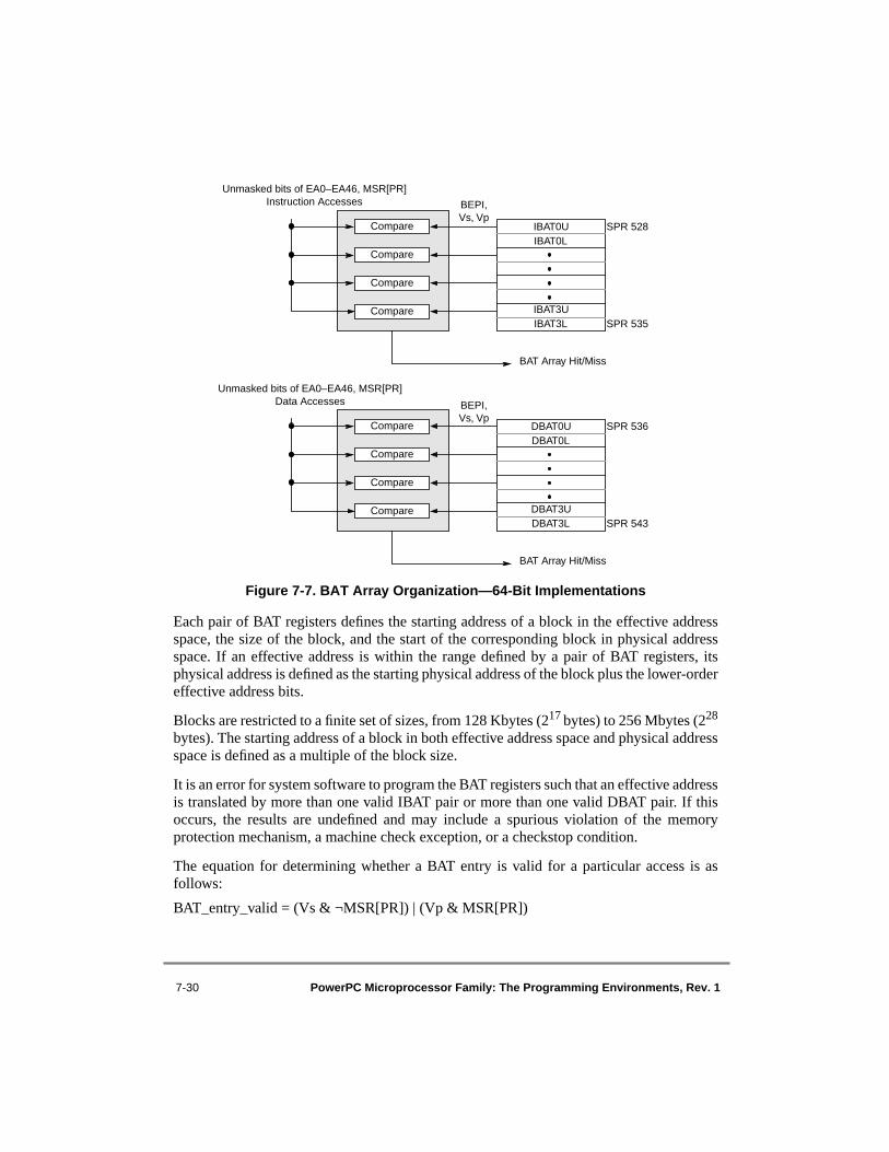
7-30 PowerPC Microprocessor Family: The Programming Environments, Rev. 1
Figure 7-7. BAT Array Organization—64-Bit Implementations
Each pair of BAT registers defines the starting address of a block in the effective addressspace, the size of the block, and the start of the corresponding block in physical addressspace. If an effective address is within the range defined by a pair of BAT registers, itsphysical address is defined as the starting physical address of the block plus the lower-ordereffective address bits.
Blocks are restricted to a finite set of sizes, from 128 Kbytes (217 bytes) to 256 Mbytes (228
bytes). The starting address of a block in both effective address space and physical addressspace is defined as a multiple of the block size.
It is an error for system software to program the BAT registers such that an effective addressis translated by more than one valid IBAT pair or more than one valid DBAT pair. If thisoccurs, the results are undefined and may include a spurious violation of the memoryprotection mechanism, a machine check exception, or a checkstop condition.
The equation for determining whether a BAT entry is valid for a particular access is asfollows:
BAT_entry_valid = (Vs & ¬MSR[PR]) | (Vp & MSR[PR])
BEPI,Vs, Vp
BEPI,Vs, Vp
Unmasked bits of EA0–EA46, MSR[PR]Instruction Accesses
BAT Array Hit/Miss
Compare
Compare
Compare
Compare
IBAT0UIBAT0L
IBAT3UIBAT3L
SPR 528
SPR 535
Unmasked bits of EA0–EA46, MSR[PR]Data Accesses
BAT Array Hit/Miss
Compare
Compare
Compare
Compare
DBAT0UDBAT0L
DBAT3UDBAT3L
SPR 536
SPR 543
Chapter 7. Memory Management 7-31
If a BAT entry is not valid for a given access, it does not participate in address translationfor that access. Two BAT entries may not map an overlapping effective address range andbe valid at the same time.
Entries that have complementary settings of V[s] and V[p] may map overlapping effectiveaddress blocks. Complementary settings would be as follows:
BAT entry A: Vs = 1, Vp = 0 BAT entry B: Vs = 0, Vp = 1
7.4.2 Recognition of Addresses in BAT ArraysThe BAT arrays are accessed in parallel with segmented address translation to determinewhether a particular effective address corresponds to a block defined by the BAT arrays. Ifan effective address is within a valid BAT area, the physical address for the memory accessis determined as described in Section 7.4.5, “Block Physical Address Generation.”
Block address translation is enabled only when address translation is enabled(MSR[IR] = 1 and/or MSR[DR] = 1). Also, a matching BAT array entry always takesprecedence over any segment descriptor translation, independent of the setting of theSTE[T] (or SR[T]) bit, and the segment descriptor information is completely ignored.
Figure 7-8 shows the flow of the BAT array comparison used in block address translationfor 64-bit implementations. When an instruction fetch operation is required, the effectiveaddress is compared with the four instruction BAT array entries; similarly, the effectiveaddresses of data accesses are compared with the four data BAT array entries. The BATarrays are fully-associative in that any of the four instruction or data BAT array entries cancontain a matching entry (for an instruction or data access, respectively).
Note that Figure 7-8 assumes that the protection bits, BATL[PP], allow an access to occur.If not, an exception is generated, as described in Section 7.4.4, “Block MemoryProtection.”
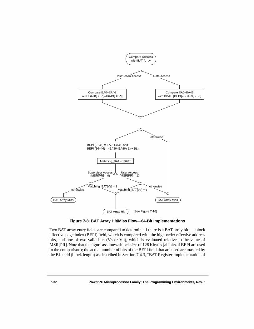
7-32 PowerPC Microprocessor Family: The Programming Environments, Rev. 1
Figure 7-8. BAT Array Hit/Miss Flow—64-Bit Implementations
Two BAT array entry fields are compared to determine if there is a BAT array hit—a blockeffective page index (BEPI) field, which is compared with the high-order effective addressbits, and one of two valid bits (Vs or Vp), which is evaluated relative to the value ofMSR[PR]. Note that the figure assumes a block size of 128 Kbytes (all bits of BEPI are usedin the comparison); the actual number of bits of the BEPI field that are used are masked bythe BL field (block length) as described in Section 7.4.3, “BAT Register Implementation of
Compare Addresswith BAT Array
Instruction Access Data Access
Compare EA0–EA46with DBAT0[BEPI]–DBAT3[BEPI]
Compare EA0–EA46with IBAT0[BEPI]–IBAT3[BEPI]
otherwise
Matching_BAT←xBATx
User Access(MSR[PR] = 1)
Supervisor Access(MSR[PR] = 0)
otherwiseMatching_BAT[Vs] = 1 otherwise
Matching_BAT[Vp] = 1
BAT Array Hit
BAT Array MissBAT Array Miss
BEPI (0–35) = EA0–EA35, andBEPI (36–46) = (EA36–EA46) & (¬ BL)
(See Figure 7-16)

Chapter 7. Memory Management 7-33
BAT Array.” Also, note that the flow for 32-bit implementations is the same as that shownin Figure 7-8 except that the effective address field to be compared with the BEPI field isEA0–EA14 instead of EA0–EA46.
Thus, the specific criteria for determining a BAT array hit are as follows:
• The upper-order 47 bits (or 15 bits for 32-bit implementations) of the effective address, subject to a mask, must match the BEPI field of the BAT array entry.
• The appropriate valid bit in the BAT array entry must set to one as follows:
— MSR[PR] = 0 corresponds to supervisor mode; in this mode, Vs is checked.— MSR[PR] = 1 corresponds to user mode; in this mode, Vp is checked.
The matching entry is then subject to the protection checking described in Section 7.4.4,“Block Memory Protection,” before it is used as the source for the physical address. Notethat if a user mode program performs an access with an effective address that matches theBEPI field of a BAT area defined as valid only for supervisor accesses (Vp = 0 and Vs = 1)for example, the BAT mechanism does not generate a protection violation and the BATentry is simply ignored. Thus, a supervisor program can use the block address translationmechanism to share a portion of the effective address space with a user program (that usespage address translation for this area).
If a memory area is to be mapped by the BAT mechanism for both instruction and dataaccesses, the mapping must be set up in both an IBAT and DBAT entry; this is the case evenon implementations that do not have separate instruction and data caches.
Note that a block can be defined to overlay part of a segment such that the block portion isnonpaged although the rest of the segment can be paged. This allows nonpaged areas to bespecified within a segment. Thus, if an area of memory is translated by an instruction BATentry and data accesses are not also required to that same area of memory, PTEs are notrequired for that area of memory. Similarly, if an area of memory is translated by a dataBAT entry, and instruction accesses are not also required to that same area of memory, PTEsare not required for that area of memory.
7.4.3 BAT Register Implementation of BAT ArrayRecall that the BAT array is comprised of four entries used for instruction accesses and fourentries used for data accesses. Each BAT array entry consists of a pair of BAT registers—anupper and a lower BAT register for each entry. The BAT registers are accessed with themtspr and mfspr instructions and are only accessible to supervisor-level programs. SeeAppendix F, “Simplified Mnemonics,” for a list of simplified mnemonics for use with theBAT registers. (Note that simplified mnemonics are referred to as extended mnemonics inthe architecture specification.)

7-34 PowerPC Microprocessor Family: The Programming Environments, Rev. 1
Figure 7-9 shows the format of the upper BAT registers and Figure 7-10 shows the formatof the lower BAT registers for 64-bit implementations.
Figure 7-9. Format of Upper BAT Registers—64-Bit Implementations
.
Figure 7-10. Format of Lower BAT Registers—64-Bit Implementations
The format and bit definitions of the upper and lower BAT registers for 32-bitimplementations are similar to that of the 64-bit implementations, and are shown inFigure 7-11 and Figure 7-12, respectively.
Figure 7-11. Format of Upper BAT Registers—32-Bit Implementations
Figure 7-12. Format of Lower BAT Registers—32-Bit Implementations
The BAT registers contain the effective-to-physical address mappings for blocks ofmemory. This mapping information includes the effective address bits that are comparedwith the effective address of the access, the memory/cache access mode bits (WIMG), andthe protection bits for the block. In addition, the size of the block and the starting addressof the block are defined by the physical block number (BRPN) and block size mask (BL)fields.
Reserved
0 46 47 50 51 61 62 63
BEPI 0 0 0 0 BL Vs Vp
BRPN 0 0 0 0 0 0 0 0 0 0 WIMG* 0 PP
Reserved
0 46 47 56 57 60 61 62 63
*W and G bits are reserved (not defined) for IBAT registers.
BEPI 0 0 0 0 BL Vs Vp
Reserved
0 14 15 18 19 29 30 31
Reserved
0 14 15 24 25 28 29 30 31
BRPN 0 0 0 0 0 0 0 0 0 0 WIMG* 0 PP
*W and G bits are not defined for IBAT registers. Attempting to write to these bits causes boundedly-undefined results.
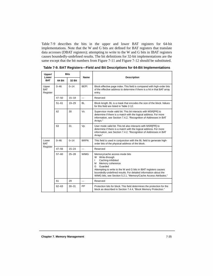
Chapter 7. Memory Management 7-35
Table 7-9 describes the bits in the upper and lower BAT registers for 64-bitimplementations. Note that the W and G bits are defined for BAT registers that translatedata accesses (DBAT registers); attempting to write to the W and G bits in IBAT registerscauses boundedly-undefined results. The bit definitions for 32-bit implementations are thesame except that the bit numbers from Figure 7-11 and Figure 7-12 should be substituted.
Table 7-9. BAT Registers—Field and Bit Descriptions for 64-Bit Implementations
Upper/LowerBAT
BitsName Description
64 Bit 32 Bit
Upper BAT Register
0–46 0–14 BEPI Block effective page index. This field is compared with high-order bits of the effective address to determine if there is a hit in that BAT array entry.
47–50 15–18 — Reserved
51–61 19–29 BL Block length. BL is a mask that encodes the size of the block. Values for this field are listed in Table 2-12.
62 30 Vs Supervisor mode valid bit. This bit interacts with MSR[PR] to determine if there is a match with the logical address. For more information, see Section 7.4.2, “Recognition of Addresses in BAT Arrays."
63 31 Vp User mode valid bit. This bit also interacts with MSR[PR] to determine if there is a match with the logical address. For more information, see Section 7.4.2, “Recognition of Addresses in BAT Arrays.”
Lower BAT Register
0–46 0–14 BRPN This field is used in conjunction with the BL field to generate high-order bits of the physical address of the block.
47–56 15–24 — Reserved
57–60 25–28 WIMG Memory/cache access mode bitsW Write-throughI Caching-inhibitedM Memory coherenceG GuardedAttempting to write to the W and G bits in IBAT registers causes boundedly-undefined results. For detailed information about the WIMG bits, see Section 5.2.1, “Memory/Cache Access Attributes."
61 29 — Reserved
62–63 30–31 PP Protection bits for block. This field determines the protection for the block as described in Section 7.4.4, “Block Memory Protection."

7-36 PowerPC Microprocessor Family: The Programming Environments, Rev. 1
The BL field in the upper BAT register is a mask that encodes the size of the block.Table 7-10 defines the bit encodings for the BL field of the upper BAT register.
Only the values shown in Table 7-10 are valid for BL. An effective address is determinedto be within a BAT area if the appropriate bits (determined by the BL field) of the effectiveaddress match the value in the BEPI field of the upper BAT register, and if the appropriatevalid bit (Vs or Vp) is set. Note that for an access to occur, the protection bits (PP bits) inthe lower BAT register must be set appropriately, as described in Section 7.4.4, “BlockMemory Protection.”
The number of zeros in the BL field determines the bits of the effective address that are usedin the comparison with the BEPI field to determine if there is a hit in that BAT array entry.The rightmost bit of the BL field is aligned with bit 46 (or bit 14 for 32-bit implementations)of the effective address; bits of the effective address corresponding to ones in the BL fieldare then cleared to zero for the comparison. For 64-bit implementations operating in 32-bitmode, the highest-order 32 bits of the effective address (EA0–EA31) are treated as zeros.
The value loaded into the BL field determines both the size of the block and the alignmentof the block in both effective address space and physical address space. The values loadedinto the BEPI and BRPN fields must have at least as many low-order zeros as there are onesin BL. Otherwise, the results are undefined. Also, if the processor does not support 64 bits(or 32 bits, for 32-bit implementations) of physical address, software should write zeros tothose unsupported bits in the BRPN field (as the implementation treats them as reserved).Otherwise, a machine check exception can occur.
Table 7-10. Upper BAT Register Block Size Mask Encodings
Block Size BL Encoding
128 Kbytes 000 0000 0000
256 Kbytes 000 0000 0001
512 Kbytes 000 0000 0011
1 Mbyte 000 0000 0111
2 Mbytes 000 0000 1111
4 Mbytes 000 0001 1111
8 Mbytes 000 0011 1111
16 Mbytes 000 0111 1111
32 Mbytes 000 1111 1111
64 Mbytes 001 1111 1111
128 Mbytes 011 1111 1111
256 Mbytes 111 1111 1111

Chapter 7. Memory Management 7-37
7.4.4 Block Memory ProtectionAfter an effective address is determined to be within a block defined by the BAT array, theaccess is validated by the memory protection mechanism. If this protection mechanismprohibits the access, a block protection violation exception condition (DSI or ISI exception)is generated.
The memory protection mechanism allows selectively granting read access, grantingread/write access, and prohibiting access to areas of memory based on a number of controlcriteria. The block protection mechanism provides protection at the granularity defined bythe block size (128 Kbyte to 256 Mbyte).
As the memory protection mechanism used by the block and page address translation isdifferent, refer to Section 7.5.4, “Page Memory Protection,” for specific information uniqueto page address translation.
For block address translation, the memory protection mechanism is controlled by the PPbits (which are located in the lower BAT register), which define the access options for theblock. Table 7-11 shows the types of accesses that are allowed for the possible PP bitcombinations.
Thus, any access attempted (read or write) when PP = 00 results in a protection violationexception condition. When PP = x1, an attempt to perform a write access causes aprotection violation exception condition, and when PP = 10, all accesses are allowed. Whenthe memory protection mechanism prohibits a reference, one of the following occurs,depending on the type of access that was attempted:
• For data accesses, a DSI exception is generated and bit 4 of DSISR is set.
• For instruction accesses, an ISI exception is generated and bit 36 of SRR1 (bit 4 in 32-bit implementations) is set.
See Chapter 6, “Exceptions,” for more information about these exceptions.
Table 7-11. Access Protection Control for Blocks
PP Accesses Allowed
00 No access
x1 Read only
10 Read/write

7-38 PowerPC Microprocessor Family: The Programming Environments, Rev. 1
Table 7-12 shows a summary of the conditions that cause exceptions for supervisor anduser read and write accesses within a BAT area. Each BAT array entry is programmed to beeither used or ignored for supervisor and user accesses via the BAT array entry valid bits,and the PP bits enforce the read/write protection options. Note that the valid bits (Vs andVp) are used as part of the match criteria for a BAT array entry and are not explicitly partof the protection mechanism.
Note that because access to the BAT registers is privileged, only supervisor programs canmodify the protection and valid bits for the block.
Table 7-12. Access Protection Summary for BAT Array
Vs VpPP
FieldBlock Type User Read User Write
Supervisor Read
Supervisor Write
0 0 xx No BAT array match Not used Not used Not used Not used
0 1 00 User—no access Exception Exception Not used Not used
0 1 x1 User-read-only √ Exception Not used Not used
0 1 10 User read/write √ √ Not used Not used
1 0 00 Supervisor—no access Not used Not used Exception Exception
1 0 x1 Supervisor-read-only Not used Not used √ Exception
1 0 10 Supervisor read/write Not used Not used √ √
1 1 00 Both—no access Exception Exception Exception Exception
1 1 x1 Both-read-only √ Exception √ Exception
1 1 10 Both read/write √ √ √ √
Note: The term ‘Not used’ implies that the access is not translated by the BAT array and is translated by the page address translation mechanism described in Section 7.5, “Memory Segment Model,” instead.
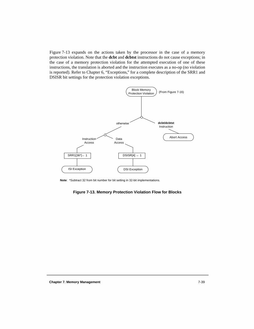
Chapter 7. Memory Management 7-39
Figure 7-13 expands on the actions taken by the processor in the case of a memoryprotection violation. Note that the dcbt and dcbtst instructions do not cause exceptions; inthe case of a memory protection violation for the attempted execution of one of theseinstructions, the translation is aborted and the instruction executes as a no-op (no violationis reported). Refer to Chapter 6, “Exceptions,” for a complete description of the SRR1 andDSISR bit settings for the protection violation exceptions.
Figure 7-13. Memory Protection Violation Flow for Blocks
DSI Exception
Block Memory Protection Violation
DSISR[4] ← 1
Abort Access
dcbt/dcbtst Instruction
otherwise
InstructionAccess
DataAccess
SRR1[36*]← 1
ISI Exception
Note: *Subtract 32 from bit number for bit setting in 32-bit implementations.
(From Figure 7-16)

7-40 PowerPC Microprocessor Family: The Programming Environments, Rev. 1
7.4.5 Block Physical Address GenerationIf the block protection mechanism validates the access, a physical address is formed asshown in Figure 7-14 for 64-bit implementations. Bits in the effective addresscorresponding to ones in the BL field, concatenated with the 17 lower-order bits of theeffective address, form the offset within the block of memory defined by the BAT arrayentry. Bits in the effective address corresponding to zeros in the BL field are then logicallyORed with the corresponding bits in the BRPN field to form the next higher-order bits ofthe physical address. Finally, the highest-order 36 bits of the BRPN field form bits 0–35 ofthe physical address (PA0–PA35).
Figure 7-14. Block Physical Address Generation—64-Bit Implementations
Block Size Mask
Physical Block Number
Effective Address
Physical Address
36 Bit 11 Bit
OR
11 Bit 17 Bit
36 Bit 11 Bit 17 Bit
0 35 36 46 47 63
AND
0 . . . . . . . . . . . . . 1
36 Bit 11 Bit 17 Bit
0 35 36 46 47 63

Chapter 7. Memory Management 7-41
The formation of physical addresses for 32-bit implementations is shown in Figure 7-15. Inthis case the highest-order four bits of the BRPN field form bits 0–3 of the physical address(PA0–PA3).
Access to the physical memory within the block is made according to the memory/cacheaccess mode defined by the WIMG bits in the lower BAT register. These bits apply to theentire block rather than to an individual page as described in Section 5.2.1,“Memory/Cache Access Attributes.”
Figure 7-15. Block Physical Address Generation—32-Bit Implementations
Physical Block Number
Effective Address
Physical Address
4 Bit 11 Bit 17 Bit
4 Bit 11 Bit
4 Bit 11 Bit 17 Bit
OR
11 Bit 17 Bit
0 3 4 14 15 31
0 3 4 14 15 31
AND
Block Size Mask 0 . . . . . . . . . . . . . 1

7-42 PowerPC Microprocessor Family: The Programming Environments, Rev. 1
7.4.6 Block Address Translation SummaryFigure 7-16 is an expansion of the ‘BAT Array Hit’ branch of Figure 7-4 and shows thetranslation of address bits for 64-bit implementations. Note that the figure does not showwhen many of the exceptions in Table 7-6 are detected or taken as this is implementation-specific.
Figure 7-16. Block Address Translation Flow—64-Bit Implementations
7.5 Memory Segment ModelMemory in the PowerPC OEA is divided into 256-Mbyte segments. This segmentedmemory model provides a way to map 4-Kbyte pages of effective addresses to 4-Kbytepages in physical memory (page address translation), while providing the programmingflexibility afforded by a large virtual address space (80 or 52 bits).
A page address translation may be superseded by a matching block address translation asdescribed in Section 7.4, “Block Address Translation.” If not, the page translation proceedsin the following two steps:
1. from effective address to the virtual address (which never exists as a specific entity but can be considered to be the concatenation of the virtual page number and the byte offset within a page), and
2. from virtual address to physical address.
The page address translation mechanism is described in the following sections, followed bya summary of page address translation with a detailed flow diagram.
Continue Access to Memory Subsystem with WIMG in Lower
BAT Register
otherwise Read Access with PP = 00
BAT Array Hit
Memory Protection Violation Flow
(See Figure 7-13)
Write Access withPP = any of
00 x1
PA0–PA63 = BRPN (0–35) ||BRPN (36–46) OR ((EA36–EA46) & (BL)) || EA47–EA63

Chapter 7. Memory Management 7-43
7.5.1 Recognition of Addresses in SegmentsThe page address translation uses segment descriptors, which provide virtual address andprotection information, and page table entries (PTEs), which provide the physical addressand page protection information. The segment descriptors are programmed by the operatingsystem to provide the virtual ID for a segment. In addition, the operating system also createsthe page table in memory that provides the virtual-to-physical address mappings (in theform of PTEs) for the pages in memory.
Segments in the OEA can be classified as one of the following two types:
• Memory segment—An effective address in these segments represents a virtual address that is used to define the physical address of the page.
• Direct-store segment—References made to direct-store segments do not use the virtual paging mechanism of the processor. Note that the direct-store facility is optional and being phased out of the architecture. See Section 7.8, “Direct-Store Segment Address Translation,” for a complete description of the mapping of direct-store segments for those processors that implement it.
The T bit in the segment descriptor selects between memory segments and direct-storesegments, as shown in Table 7-13.
7.5.1.1 Selection of Memory SegmentsAll accesses generated by the processor can be mapped to a segment descriptor; however,if translation is disabled (MSR[IR] = 0 or MSR[DR] = 0 for an instruction or data access,respectively), real addressing mode translation is performed as described in Section 7.3,“Real Addressing Mode.” Otherwise, if T = 0 in the corresponding segment descriptor (andthe address is not translated by the BAT mechanism), the access maps to memory space andpage address translation is performed.
After a memory segment is selected, the processor creates the virtual address for thesegment and searches for the PTE that dictates the physical page number to be used for theaccess. Note that I/O devices can be easily mapped into memory space and used asmemory-mapped I/O.
Table 7-13. Segment Descriptor Types
Segment Descriptor T Bit
Segment Type
0 Memory segment
1 Direct-store segment—optional, but being phased out of the architecture. Its use is discouraged.
7-44 PowerPC Microprocessor Family: The Programming Environments, Rev. 1
7.5.1.2 Selection of Direct-Store SegmentsAs described for memory segments, all accesses generated by the processor (withtranslation enabled) map to a segment descriptor. If T = 1 for the selected segmentdescriptor, the access maps to the direct-store interface space and the access proceeds asdescribed in Section 7.8, “Direct-Store Segment Address Translation.” Because the direct-store interface is present only for compatibility with existing I/O devices that used thisinterface and because the direct-store interface protocol is not optimized for performance,its use is discouraged. Additionally, the direct-store facility is being phased out of thearchitecture and future devices are not likely to support it. Thus, software should not dependon its results and new software should not use it. The most efficient method for accessingI/O is by mapping the I/O areas to memory segments.
7.5.2 Page Address Translation OverviewThe first step in page address translation for 64-bit implementations is the conversion of the64-bit effective address of an access into the 80-bit (or 64-bit) virtual address. The virtualaddress is then used to locate the PTE in the page table in memory. The physical pagenumber is then extracted from the PTE and used in the formation of the physical address ofthe access. Note that for increased performance, some processors may implement on-chipTLBs to store copies of recently-used PTEs.
Figure 7-17 shows an overview of the translation of an effective address to a physicaladdress for 64-bit implementations as follows:
• Bits 0–35 of the effective address comprise the effective segment ID used to select a segment descriptor, from which the virtual segment ID (VSID) is extracted.
• Bits 36–51 of the effective address correspond to the page number within the segment; these are concatenated with the VSID from the segment descriptor to form the virtual page number (VPN). The VPN is used to search for the PTE in either an on-chip TLB or the page table. The PTE then provides the physical page number (RPN). Note that bits 36–40 form the abbreviated page index (API) which is used to compare with page table entries during hashing. This is described in detail in Section 7.6.1.7.1, “PTEG Address Mapping Example—64-Bit Implementation.”
• Bits 52–63 of the effective address are the byte offset within the page; these are concatenated with the RPN field of a PTE to form the physical address used to access memory.

Chapter 7. Memory Management 7-45
Figure 7-17. Page Address Translation Overview—64-Bit Implementations
TEMPORARY 64-BIT BRIDGE
Because processors that implement the 64-bit bridge access only a 32-bit address space,only 16 STEs are required to define the entire 4-Gbyte address space. Page addresstranslation for 64-bit processors using the 64-bit bridge uses a subset of the functionalitydescribed here for 64-bit implementations. For example, only bits 32–35 are used to selecta segment descriptor, and as in the 32-bit portion of the architecture, only 16 on-chipsegment registers are required. These segment descriptors are maintained in 16 SLBentries.
For details concerning the 64-bit bridge, see Section 7.9, “Migration of Operating Systemsfrom 32-Bit Implementations to 64-Bit Implementations.”
80-Bit Virtual Address
64-Bit Effective Address
64-Bit Physical Address
API Byte Offset(5 Bit) (12 Bit)
Virtual Segment ID (VSID) Page Index Byte Offset(52 Bit) (16 Bit) (12 Bit)
Physical Page Number (RPN) Byte Offset(52 Bit) (12 Bit)
TLB/Page Table
Page Index (16-bit)
PTE
0 35 36 51 52 63
SLB/Segment Table
0 51 52 67 68 79
Virtual Page Number (VPN)
Effective Segment ID(36 Bit)
0 51 52 63
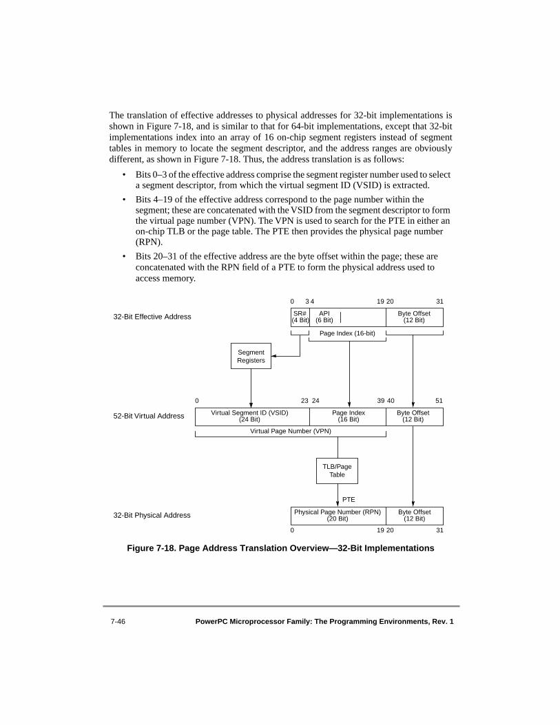
7-46 PowerPC Microprocessor Family: The Programming Environments, Rev. 1
The translation of effective addresses to physical addresses for 32-bit implementations isshown in Figure 7-18, and is similar to that for 64-bit implementations, except that 32-bitimplementations index into an array of 16 on-chip segment registers instead of segmenttables in memory to locate the segment descriptor, and the address ranges are obviouslydifferent, as shown in Figure 7-18. Thus, the address translation is as follows:
• Bits 0–3 of the effective address comprise the segment register number used to select a segment descriptor, from which the virtual segment ID (VSID) is extracted.
• Bits 4–19 of the effective address correspond to the page number within the segment; these are concatenated with the VSID from the segment descriptor to form the virtual page number (VPN). The VPN is used to search for the PTE in either an on-chip TLB or the page table. The PTE then provides the physical page number (RPN).
• Bits 20–31 of the effective address are the byte offset within the page; these are concatenated with the RPN field of a PTE to form the physical address used to access memory.
Figure 7-18. Page Address Translation Overview—32-Bit Implementations
52-Bit Virtual Address
32-Bit Effective Address
32-Bit Physical Address
SR# API Byte Offset(4 Bit) (6 Bit) (12 Bit)
Virtual Segment ID (VSID) Page Index Byte Offset(24 Bit) (16 Bit) (12 Bit)
Physical Page Number (RPN) Byte Offset(20 Bit) (12 Bit)
TLB/Page Table
Page Index (16-bit)
PTE
0 3 4 19 20 31
Segment Registers
0 23 24 39 40 51
Virtual Page Number (VPN)
0 19 20 31
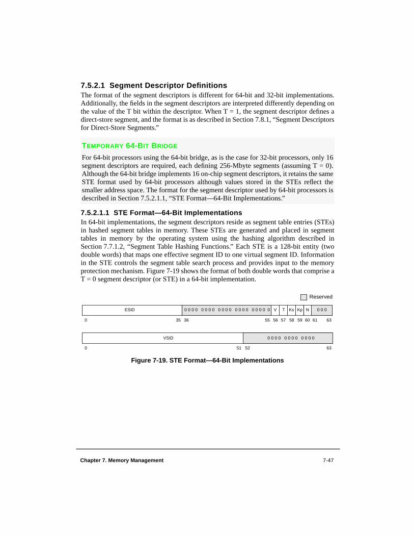
Chapter 7. Memory Management 7-47
7.5.2.1 Segment Descriptor DefinitionsThe format of the segment descriptors is different for 64-bit and 32-bit implementations.Additionally, the fields in the segment descriptors are interpreted differently depending onthe value of the T bit within the descriptor. When T = 1, the segment descriptor defines adirect-store segment, and the format is as described in Section 7.8.1, “Segment Descriptorsfor Direct-Store Segments.”
7.5.2.1.1 STE Format—64-Bit ImplementationsIn 64-bit implementations, the segment descriptors reside as segment table entries (STEs)in hashed segment tables in memory. These STEs are generated and placed in segmenttables in memory by the operating system using the hashing algorithm described inSection 7.7.1.2, “Segment Table Hashing Functions.” Each STE is a 128-bit entity (twodouble words) that maps one effective segment ID to one virtual segment ID. Informationin the STE controls the segment table search process and provides input to the memoryprotection mechanism. Figure 7-19 shows the format of both double words that comprise aT = 0 segment descriptor (or STE) in a 64-bit implementation.
Figure 7-19. STE Format—64-Bit Implementations
TEMPORARY 64-BIT BRIDGE
For 64-bit processors using the 64-bit bridge, as is the case for 32-bit processors, only 16segment descriptors are required, each defining 256-Mbyte segments (assuming T = 0).Although the 64-bit bridge implements 16 on-chip segment descriptors, it retains the sameSTE format used by 64-bit processors although values stored in the STEs reflect thesmaller address space. The format for the segment descriptor used by 64-bit processors isdescribed in Section 7.5.2.1.1, “STE Format—64-Bit Implementations.”
Reserved
0 35 36 55 56 57 58 59 60 61 63
0 51 52 63
ESID 0 0 0 0 0 0 0 0 0 0 0 0 0 0 0 0 0 0 0 0 0 V T Ks Kp N 0 0 0
VSID 0 0 0 0 0 0 0 0 0 0 0 0
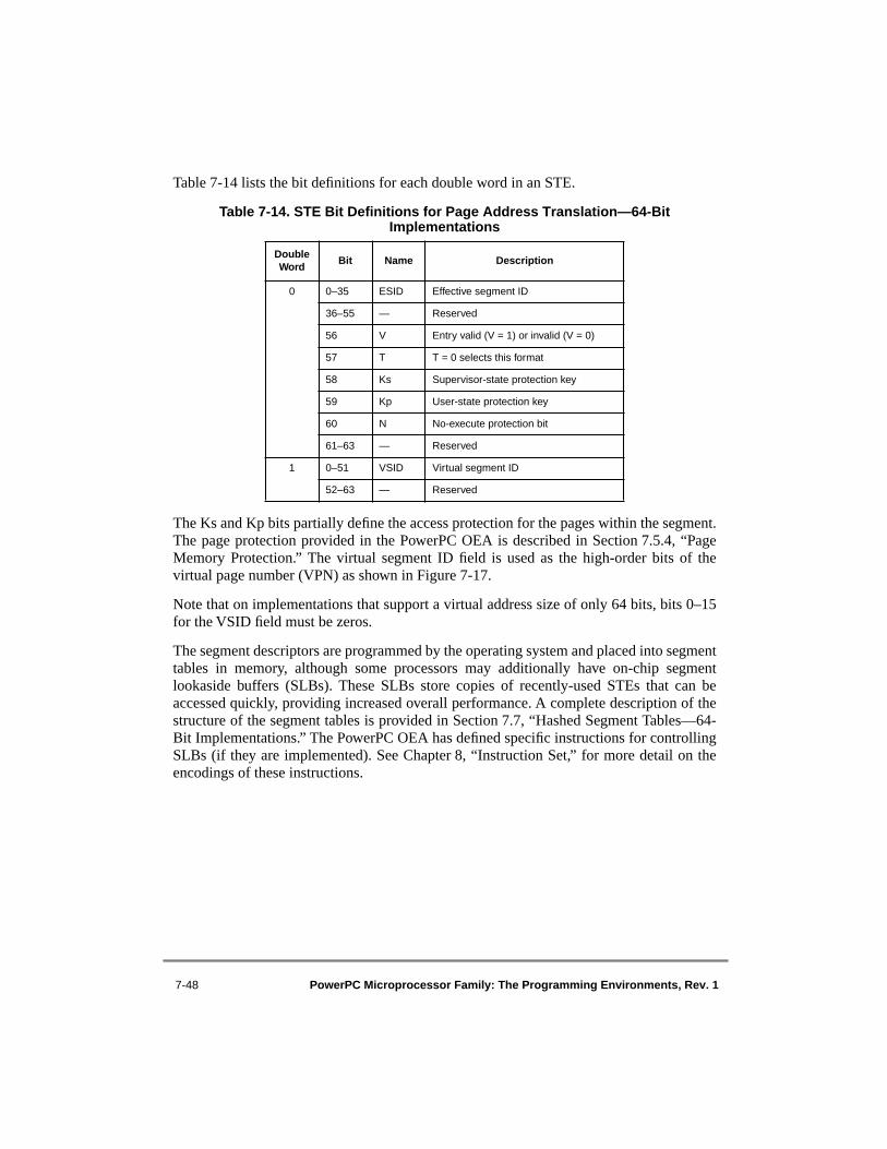
7-48 PowerPC Microprocessor Family: The Programming Environments, Rev. 1
Table 7-14 lists the bit definitions for each double word in an STE.
The Ks and Kp bits partially define the access protection for the pages within the segment.The page protection provided in the PowerPC OEA is described in Section 7.5.4, “PageMemory Protection.” The virtual segment ID field is used as the high-order bits of thevirtual page number (VPN) as shown in Figure 7-17.
Note that on implementations that support a virtual address size of only 64 bits, bits 0–15for the VSID field must be zeros.
The segment descriptors are programmed by the operating system and placed into segmenttables in memory, although some processors may additionally have on-chip segmentlookaside buffers (SLBs). These SLBs store copies of recently-used STEs that can beaccessed quickly, providing increased overall performance. A complete description of thestructure of the segment tables is provided in Section 7.7, “Hashed Segment Tables—64-Bit Implementations.” The PowerPC OEA has defined specific instructions for controllingSLBs (if they are implemented). See Chapter 8, “Instruction Set,” for more detail on theencodings of these instructions.
Table 7-14. STE Bit Definitions for Page Address Translation—64-Bit Implementations
Double Word
Bit Name Description
0 0–35 ESID Effective segment ID
36–55 — Reserved
56 V Entry valid (V = 1) or invalid (V = 0)
57 T T = 0 selects this format
58 Ks Supervisor-state protection key
59 Kp User-state protection key
60 N No-execute protection bit
61–63 — Reserved
1 0–51 VSID Virtual segment ID
52–63 — Reserved

Chapter 7. Memory Management 7-49
7.5.2.1.2 Segment Descriptor Format—32-Bit ImplementationsIn 32-bit implementations, the segment descriptors are 32 bits long and reside in one of 16on-chip segment registers. Figure 7-20 shows the format of a segment register used in pageaddress translation (T = 0) in a 32-bit implementation.
Figure 7-20. Segment Register Format for Page Address Translation—32-Bit Implementations
Table 7-15 provides the corresponding bit definitions of the segment register in 32-bitimplementations.
The Ks and Kp bits partially define the access protection for the pages within the segment.The page protection provided in the PowerPC OEA is described in Section 7.5.4, “PageMemory Protection.” The virtual segment ID field is used as the high-order bits of thevirtual page number (VPN) as shown in Figure 7-18.
TEMPORARY 64-BIT BRIDGE
Note that processors using the 64-bit bridge implement STEs as defined for 64-bitimplementations as described in this section, however, from a software perspective thefunction of these segment descriptors is indistinguishable from the segment registers asthey are defined for 32-bit implementations. However, the values in the STEs reflect onlya 32-bit address space. For example, the ESID field uses only four bits (ESID[32–35]),which, like the four highest-order bits in a 32-bit effective address, provide an index to oneof the 16 segment descriptors.
Table 7-15. Segment Register Bit Definition for Page Address Translation—32-Bit Implementations
Bit Name Description
0 T T = 0 selects this format
1 Ks Supervisor-state protection key
2 Kp User-state protection key
3 N No-execute protection bit
4–7 — Reserved
8–31 VSID Virtual segment ID
0 1 2 3 4 7 8 31
T Ks Kp N 0 0 0 0 VSID
Reserved

7-50 PowerPC Microprocessor Family: The Programming Environments, Rev. 1
The segment registers are programmed with specific instructions that reference the segmentregisters. However, since the segment registers described here are merely a conceptualmodel, a processor may implement separate segment registers for instructions and for data,for example. In this case, it is the responsibility of the hardware to maintain the consistencybetween the multiple sets of segment registers.
The segment register instructions are summarized in Table 7-16. These instructions areprivileged in that they are executable only while operating in supervisor mode. SeeSection 2.3.18, “Synchronization Requirements for Special Registers and for LookasideBuffers,” for information about the synchronization requirements when modifying thesegment registers. See Chapter 8, “Instruction Set,” for more detail on the encodings ofthese instructions.
Table 7-16. Segment Register Instructions—32-Bit Implementations
Instruction Description
mtsr SR,rS Move to Segment RegisterSR[SR]← rS
mtsrin rS,rB Move to Segment Register IndirectSR[rB[0–3]]←rS
mfsr rD,SR Move from Segment RegisterrD←SR[SR]
mfsrin rD,rB Move from Segment Register IndirectrD←SR[rB[0–3]]
Note: These instructions apply only to 32-bit implementations and 64-bit processors that implement the 64-bit bridge.
TEMPORARY 64-BIT BRIDGE
Note that segment registers and the instructions listed in Table 7-16 are intended for use in32-bit implementations. In 64-bit implementations, these instructions are legal only inprocessors that support the 64-bit bridge architecture described in Section 7.9, “Migrationof Operating Systems from 32-Bit Implementations to 64-Bit Implementations.” However,if these features are not supported, attempting to execute these instructions on a 64-bitimplementation causes an illegal instruction program exception.

Chapter 7. Memory Management 7-51
7.5.2.2 Page Table Entry (PTE) DefinitionsPage table entries (PTEs) are generated and placed in page table in memory by theoperating system using the hashing algorithm described in Section 7.6.1.3, “Page TableHashing Functions.” The PowerPC OEA defines similar PTE formats for both 64- and 32-bit implementations in that the same fields are defined. However, 64-bit implementationsdefine PTEs that are 128 bits in length while 32-bit implementations define PTEs that are64 bits in length. Additionally, care must be taken when programming for both 64- and 32-bit implementations, as the bit placements of some fields are different. Some of the fieldsare defined as follows:
• The virtual segment ID field corresponds to the high-order bits of the virtual page number (VPN), and, along with the H, V, and API fields, it is used to locate the PTE (used as match criteria in comparing the PTE with the segment information).
• The R and C bits maintain history information for the page as described in Section 7.5.3, “Page History Recording.”
• The WIMG bits define the memory/cache control mode for accesses to the page.
• The PP bits define the remaining access protection constraints for the page. The page protection provided by PowerPC processors is described in Section 7.5.4, “Page Memory Protection.”
Conceptually, the page table in memory must be searched to translate the address of everyreference. For performance reasons, however, some processors use on-chip TLBs to cachecopies of recently-used PTEs so that the table search time is eliminated for most accesses.In this case, the TLB is searched for the address translation first. If a copy of the PTE isfound, then no page table search is performed. As TLBs are noncoherent caches of PTEs,software that changes the page table in any way must perform the appropriate TLBinvalidate operations to keep the on-chip TLBs coherent with respect to the page table inmemory.
7.5.2.2.1 PTE Format for 64-Bit ImplementationsIn 64-bit implementations, each PTE is a 128-bit entity (two double words) that maps avirtual page number (VPN) to a physical page number (RPN). Information in the PTE isused in the page table search process (to determine a page table hit) and provides input tothe memory protection mechanism. Figure 7-21 shows the format of the two double wordsthat comprise a PTE for 64-bit implementations.
Figure 7-21. Page Table Entry Format—64-Bit Implementations
Reserved
0 51 52 54 55 56 57 60 61 62 63
0 51 52 56 57 61 62 63
RPN 0 0 0 R C WIMG 0 PP
VSID API 0 0 0 0 0 H V

7-52 PowerPC Microprocessor Family: The Programming Environments, Rev. 1
Table 7-17 lists the corresponding bit definitions for each double word in a PTE as defined.
The PTE contains an abbreviated page index rather than the complete page index fieldbecause at least 11 of the low-order bits of the page index are used in the hash function toselect a PTE group (PTEG) address (PTEG addresses define the location of a PTE).Therefore, these 11 lower-order bits are not repeated in the PTEs of that PTEG.
Note that on implementations that support a virtual address size of only 64 bits, bits 0–15of the VSID field must be zeros.
7.5.2.2.2 PTE Format for 32-Bit ImplementationsFigure 7-22 shows the format of the two words that comprise a PTE for 32-bitimplementations.
Figure 7-22. Page Table Entry Format—32-Bit Implementations
Table 7-18 lists the corresponding bit definitions for each word in a PTE as defined above.
Table 7-17. PTE Bit Definitions—64-Bit Implementations
Double Word Bit Name Description
0 0–51 VSID Virtual segment ID—corresponds to the high-order bits of the virtual page number (VPN)
52–56 API Abbreviated page index
57–61 — Reserved
62 H Hash function identifier
63 V Entry valid (V = 1) or invalid (V = 0)
1 0–51 RPN Physical page number
52–54 — Reserved
55 R Referenced bit
56 C Changed bit
57–60 WIMG Memory/cache access control bits
61 — Reserved
62–63 PP Page protection bits
Reserved
0 19 20 22 23 24 25 28 29 30 31
V VSID H API
0 1 24 25 26 31
RPN 000 R C WIMG 0 PP
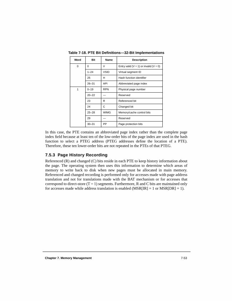
Chapter 7. Memory Management 7-53
In this case, the PTE contains an abbreviated page index rather than the complete pageindex field because at least ten of the low-order bits of the page index are used in the hashfunction to select a PTEG address (PTEG addresses define the location of a PTE).Therefore, these ten lower-order bits are not repeated in the PTEs of that PTEG.
7.5.3 Page History RecordingReferenced (R) and changed (C) bits reside in each PTE to keep history information aboutthe page. The operating system then uses this information to determine which areas ofmemory to write back to disk when new pages must be allocated in main memory.Referenced and changed recording is performed only for accesses made with page addresstranslation and not for translations made with the BAT mechanism or for accesses thatcorrespond to direct-store (T = 1) segments. Furthermore, R and C bits are maintained onlyfor accesses made while address translation is enabled (MSR[IR] = 1 or MSR[DR] = 1).
Table 7-18. PTE Bit Definitions—32-Bit Implementations
Word Bit Name Description
0 0 V Entry valid (V = 1) or invalid (V = 0)
1–24 VSID Virtual segment ID
25 H Hash function identifier
26–31 API Abbreviated page index
1 0–19 RPN Physical page number
20–22 — Reserved
23 R Referenced bit
24 C Changed bit
25–28 WIMG Memory/cache control bits
29 — Reserved
30–31 PP Page protection bits

7-54 PowerPC Microprocessor Family: The Programming Environments, Rev. 1
In general, the referenced and changed bits are updated to reflect the status of the pagebased on the access, as shown in Table 7-19.
In processors that implement a TLB, the processor may perform the R and C bit updatesbased on the copies of these bits resident in the TLB. For example, the processor mayupdate the C bit based only on the status of the C bit in the TLB entry in the case of a TLBhit (the R bit may be assumed to be set in the page tables if there is a TLB hit). Therefore,when software clears the R and C bits in the page tables in memory, it must invalidate theTLB entries associated with the pages whose referenced and changed bits were cleared. SeeSection 7.6.3, “Page Table Updates,” for all of the constraints imposed on the softwarewhen updating the referenced and changed bits in the page tables.
The R bit for a page may be set by the execution of the dcbt or dcbtst instruction to thatpage. However, neither of these instructions cause the C bit to be set.
The update of the referenced and changed bits is performed by PowerPC processors as ifaddress translation were disabled (real addressing mode address).
7.5.3.1 Referenced BitThe referenced bit for each virtual page is located in the PTE. Every time a page isreferenced (by an instruction fetch, or any other read or write access) the referenced bit isset in the page table. The referenced bit may be set immediately, or the setting may bedelayed until the memory access is determined to be successful. Because the reference to apage is what causes a PTE to be loaded into the TLB, some processors may assume the Rbit in the TLB is always set. The processor never automatically clears the referenced bit.
The referenced bit is only a hint to the operating system about the activity of a page. Attimes, the referenced bit may be set although the access was not logically required by theprogram or even if the access was prevented by memory protection. Examples of thisinclude the following:
• Fetching of instructions not subsequently executed• Accesses generated by an lswx or stswx instruction with a zero length• Accesses generated by a stwcx. or stdcx. instruction when no store is performed • Accesses that cause exceptions and are not completed
Table 7-19. Table Search Operations to Update History Bits
R and C bits Processor Action
00 Read: Table search operation to update R Write: Table search operation to update R and C
01 Combination doesn’t occur
10 Read: No special actionWrite: Table search operation to update C
11 No special action for read or write
Chapter 7. Memory Management 7-55
7.5.3.2 Changed BitThe changed bit for each virtual page is located both in the PTE in the page table and in thecopy of the PTE loaded into the TLB (if a TLB is implemented). Whenever a data storeinstruction is executed successfully, if the TLB search (for page address translation) resultsin a hit, the changed bit in the matching TLB entry is checked. If it is already set, theprocessor does not change the C bit. If the TLB changed bit is 0, it is set and a table searchoperation is performed to set the C bit in the corresponding PTE in the page table.
Processors cause the changed bit (in both the PTE in the page tables and in the TLB ifimplemented) to be set only when a store operation is allowed by the page memoryprotection mechanism and the store is guaranteed to be in the execution path, unless anexception, other than those caused by one of the following occurs:
• System-caused interrupts (system reset, machine check, external, and decrementer interrupts)
• Floating-point enabled exception type program exceptions when the processor is in an imprecise mode
• Floating-point assist exceptions for instructions that cause no other kind of precise exception
Furthermore, the following conditions may cause the C bit to be set:
• The execution of an stwcx. or stdcx. instruction is allowed by the memory protection mechanism but a store operation is not performed.
• The execution of an stswx instruction is allowed by the memory protection mechanism but a store operation is not performed because the specified length is zero.
• A dcba or dcbi instruction is executed.
No other cases cause the C bit to be set.
7.5.3.3 Scenarios for Referenced and Changed Bit RecordingThis section provides a summary of the model (defined by the OEA) used by PowerPCprocessors that maintain the referenced and changed bits automatically in hardware, in thesetting of the R and C bits. In some scenarios, the bits are guaranteed to be set by theprocessor; in some scenarios, the architecture allows that the bits may be set (not absolutelyrequired); and in some scenarios, the bits are guaranteed to not be set. Note that when thehardware updates the R and C bits in memory, the accesses are performed as a physicalmemory access, as if the WIMG bit settings were 0b0010 (that is, as unguarded cacheableoperations in which coherency is required).
In implementations that do not maintain the R and C bits in hardware, software assistanceis required. For these processors, the information in this section still applies, except that thesoftware performing the updates is constrained to the rules described (that is, must set bitsshown as guaranteed to be set and must not set bits shown as guaranteed to not be set). Note

7-56 PowerPC Microprocessor Family: The Programming Environments, Rev. 1
that this software should be contained in the area of memory reserved for implementation-specific use and should be invisible to the operating system.
Table 7-20 defines a prioritized list of the R and C bit settings for all scenarios. The entriesin the table are prioritized from top to bottom, such that a matching scenario occurringcloser to the top of the table takes precedence over a matching scenario closer to the bottomof the table. For example, if an stwcx. instruction causes a protection violation and there isno reservation, the C bit is not altered, as shown for the protection violation case. Note thatin the table, load operations include those generated by load instructions, by the eciwxinstruction, and by the cache management instructions that are treated as loads with respectto address translation. Similarly, store operations include those operations generated bystore instructions, by the ecowx instruction, and by the cache management instructions thatare treated as stores with respect to address translation.
Table 7-20. Model for Guaranteed R and C Bit Settings
Priority ScenarioCauses Setting
of R Bit Causes Setting
of C Bit
1 No-execute protection violation No No
2 Page protection violation Maybe No
3 Out-of-order instruction fetch or load operation Maybe No
4 Out-of-order store operation for instructions that will cause no other kind of precise exception (in the absence of system-caused, imprecise, or floating-point assist exceptions)
Maybe1 Maybe1
5 All other out-of-order store operations Maybe1 No
6 Zero-length load (lswx) Maybe No
7 Zero-length store (stswx) Maybe1 Maybe1
8 Store conditional (stwcx., or stdcx.) that does not store
Maybe1 Maybe1
9 In-order instruction fetch Yes2 No
10 Load instruction or eciwx Yes No
11 Store instruction, ecowx, dcbz, or dcba 3 instruction Yes Yes
12 icbi, dcbt, dcbtst, dcbst, or dcbf instruction Maybe No
13 dcbi instruction Maybe1 Maybe1
Notes: 1 If C is set, R is guaranteed to also be set.2 This includes the case in which the instruction was fetched out of order and R was not set.3 For a dcba instruction that does not modify the target block, it is possible that neither bit is set.

Chapter 7. Memory Management 7-57
7.5.3.4 Synchronization of Memory Accesses and Referenced and Changed Bit Updates
Although the processor updates the referenced and changed bits in the page tablesautomatically, these updates are not guaranteed to be immediately visible to the programafter the load, store, or instruction fetch operation that caused the update. If processor Aexecutes a load or store or fetches an instruction, the following conditions are met withrespect to performing the access and performing any R and C bit updates:
• If processor A subsequently executes a sync instruction, both the updates to the bits in the page table and the load or store operation are guaranteed to be performed with respect to all processors and mechanisms before the sync instruction completes on processor A.
• Additionally, if processor B executes a tlbie instruction that
— signals the invalidation to the hardware,
— invalidates the TLB entry for the access in processor A, and
— is detected by processor A after processor A has begun the access,and processor B executes a tlbsync instruction after it executes the tlbie, both the updates to the bits and the original access are guaranteed to be performed with respect to all processors and mechanisms before the tlbsync instruction completes on processor A.
7.5.4 Page Memory ProtectionIn addition to the no-execute option that can be programmed at the segment descriptor levelto prevent instructions from being fetched from a given segment (shown in Figure 7-5),there are a number of other memory protection options that can be programmed at the pagelevel. The page memory protection mechanism allows selectively granting read access,granting read/write access, and prohibiting access to areas of memory based on a numberof control criteria.
The memory protection used by the block and page address translation mechanisms isdifferent in that the page address translation protection defines a key bit that, in conjunctionwith the PP bits, determines whether supervisor and user programs can access a page. Forspecific information about block address translation, refer to Section 7.4.4, “BlockMemory Protection.”
For page address translation, the memory protection mechanism is controlled by thefollowing:
• MSR[PR], which defines the mode of the access as follows:
— MSR[PR] = 0 corresponds to supervisor mode — MSR[PR] = 1 corresponds to user mode
• Ks and Kp, the supervisor and user key bits, which define the key for the page
• The PP bits, which define the access options for the page

7-58 PowerPC Microprocessor Family: The Programming Environments, Rev. 1
The key bits (Ks and Kp) and the PP bits are located as follows for page address translation:
• Ks and Kp are located in the segment descriptor.
• The PP bits are located in the PTE.
The key bits, the PP bits, and the MSR[PR] bit are used as follows:
• When an access is generated, one of the key bits is selected to be the key as follows:
— For supervisor accesses (MSR[PR] = 0), the Ks bit is used and Kp is ignored— For user accesses (MSR[PR] = 1), the Kp bit is used and Ks is ignored
That is, key = (Kp & MSR[PR]) | (Ks & ¬MSR[PR])
• The selected key is used with the PP bits to determine if instruction fetching, load access, or store access is allowed.
Table 7-21 shows the types of accesses that are allowed for the general case (all possibleKs, Kp, and PP bit combinations), assuming that the N bit in the segment descriptor iscleared (the no-execute option is not selected).
Thus, the conditions that cause a protection violation (not including the no-executeprotection option for instruction fetches) are depicted in Table 7-22 and as a flow diagramin Figure 7-25. Any access attempted (read or write) when the key = 1 and PP = 00, causesa protection violation exception condition. When key = 1 and PP = 01, an attempt toperform a write access causes a protection violation exception condition. When PP = 10, allaccesses are allowed, and when PP = 11, write accesses always cause an exception. Theprocessor takes either the ISI or the DSI exception (for an instruction or data access,respectively) when there is an attempt to violate the memory protection.
Table 7-21. Access Protection Control with Key
Key1 PP2 Page Type
0 00 Read/write
0 01 Read/write
0 10 Read/write
0 11 Read only
1 00 No access
1 01 Read only
1 10 Read/write
1 11 Read only
Notes: 1 Ks or Kp selected by state of MSR[PR] 2 PP protection option bits in PTE

Chapter 7. Memory Management 7-59
Any combination of the Ks, Kp, and PP bits is allowed. One example is if the Ks and Kpbits are programmed so that the value of the key bit for Table 7-21 directly matches theMSR[PR] bit for the access. In this case, the encoding of Ks = 0 and Kp = 1 is used for thePTE, and the PP bits then enforce the protection options shown in Table 7-23.
However, if the setting Ks = 1 is used, supervisor accesses are treated as user reads andwrites with respect to Table 7-23. Likewise, if the setting Kp = 0 is used, user accesses tothe page are treated as supervisor accesses in relation to Table 7-23. Therefore, bymodifying one of the key bits (in the segment descriptor), the way the processor interpretsaccesses (supervisor or user) in a particular segment can easily be changed. Note, however,that only supervisor programs are allowed to modify the key bits for the segment descriptor.For 64-bit implementations, although access to the ASR is privileged, the operating systemmust protect write accesses to the segment table as well. For 32-bit implementations, accessto the segment registers is privileged.
Table 7-22. Exception Conditions for Key and PP Combinations
Key PPProhibited Accesses
0 0x None
1 00 Read/write
1 01 Write
x 10 None
x 11 Write
Table 7-23. Access Protection Encoding of PP Bits for Ks = 0 and Kp = 1
PP Field
OptionUser Read(Key = 1)
User Write(Key = 1)
Supervisor Read
(Key = 0)
Supervisor Write
(Key = 0)
00 Supervisor-only Violation Violation √ √
01 Supervisor-write-only √ Violation √ √
10 Both user/supervisor √ √ √ √
11 Both read-only √ Violation √ Violation
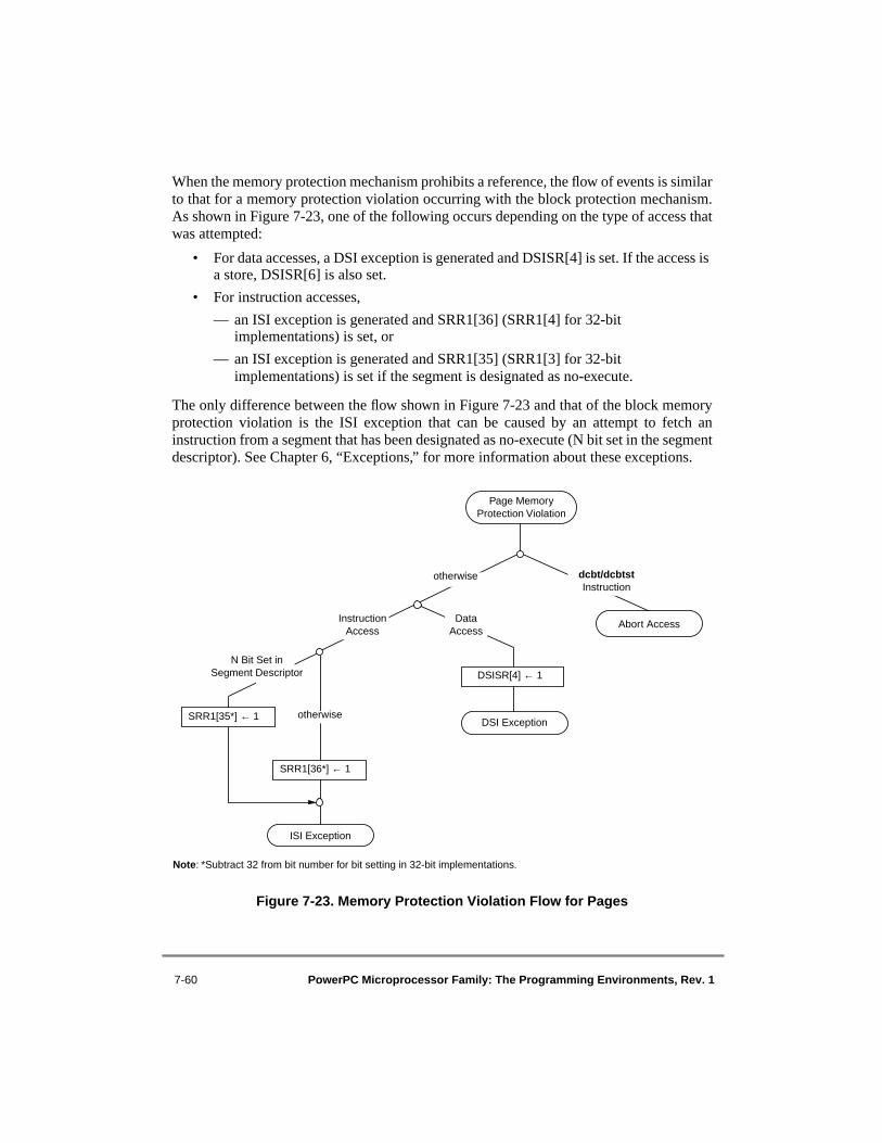
7-60 PowerPC Microprocessor Family: The Programming Environments, Rev. 1
When the memory protection mechanism prohibits a reference, the flow of events is similarto that for a memory protection violation occurring with the block protection mechanism.As shown in Figure 7-23, one of the following occurs depending on the type of access thatwas attempted:
• For data accesses, a DSI exception is generated and DSISR[4] is set. If the access is a store, DSISR[6] is also set.
• For instruction accesses,
— an ISI exception is generated and SRR1[36] (SRR1[4] for 32-bit implementations) is set, or
— an ISI exception is generated and SRR1[35] (SRR1[3] for 32-bit implementations) is set if the segment is designated as no-execute.
The only difference between the flow shown in Figure 7-23 and that of the block memoryprotection violation is the ISI exception that can be caused by an attempt to fetch aninstruction from a segment that has been designated as no-execute (N bit set in the segmentdescriptor). See Chapter 6, “Exceptions,” for more information about these exceptions.
Figure 7-23. Memory Protection Violation Flow for Pages
DSI Exception
Page Memory Protection Violation
DSISR[4] ← 1
Abort Access
dcbt/dcbtst Instruction
otherwise
InstructionAccess
DataAccess
SRR1[36*] ← 1
ISI Exception
otherwise
N Bit Set inSegment Descriptor
SRR1[35*] ← 1
Note: *Subtract 32 from bit number for bit setting in 32-bit implementations.
Chapter 7. Memory Management 7-61
If the page protection mechanism prohibits a store operation, the changed bit is not set (ineither the TLB or in the page tables in memory); however, a prohibited store access maycause a PTE to be loaded into the TLB and consequently cause the referenced bit to be setin a PTE (both in the TLB and in the page table in memory).
7.5.5 Page Address Translation SummaryFigure 7-24 provides the detailed flow for the page address translation mechanism in 64-bitimplementations. The figure includes the checking of the N bit in the segment descriptorand then expands on the ‘TLB Hit’ branch of Figure 7-5. The detailed flow for the ‘TLBMiss’ branch of Figure 7-5 is described in Section 7.6.2, “Page Table Search Operation.”The checking of memory protection violation conditions for page address translation isshown in Figure 7-25. The ‘Invalidate TLB Entry’ box shown in Figure 7-24 is marked asimplementation-specific as this level of detail for TLBs (and the existence of TLBs) is notdictated by the architecture. Note that the figure does not show the detection of all exceptionconditions shown in Table 7-5 and Table 7-6; the flow for many of these exceptions isimplementation-specific.
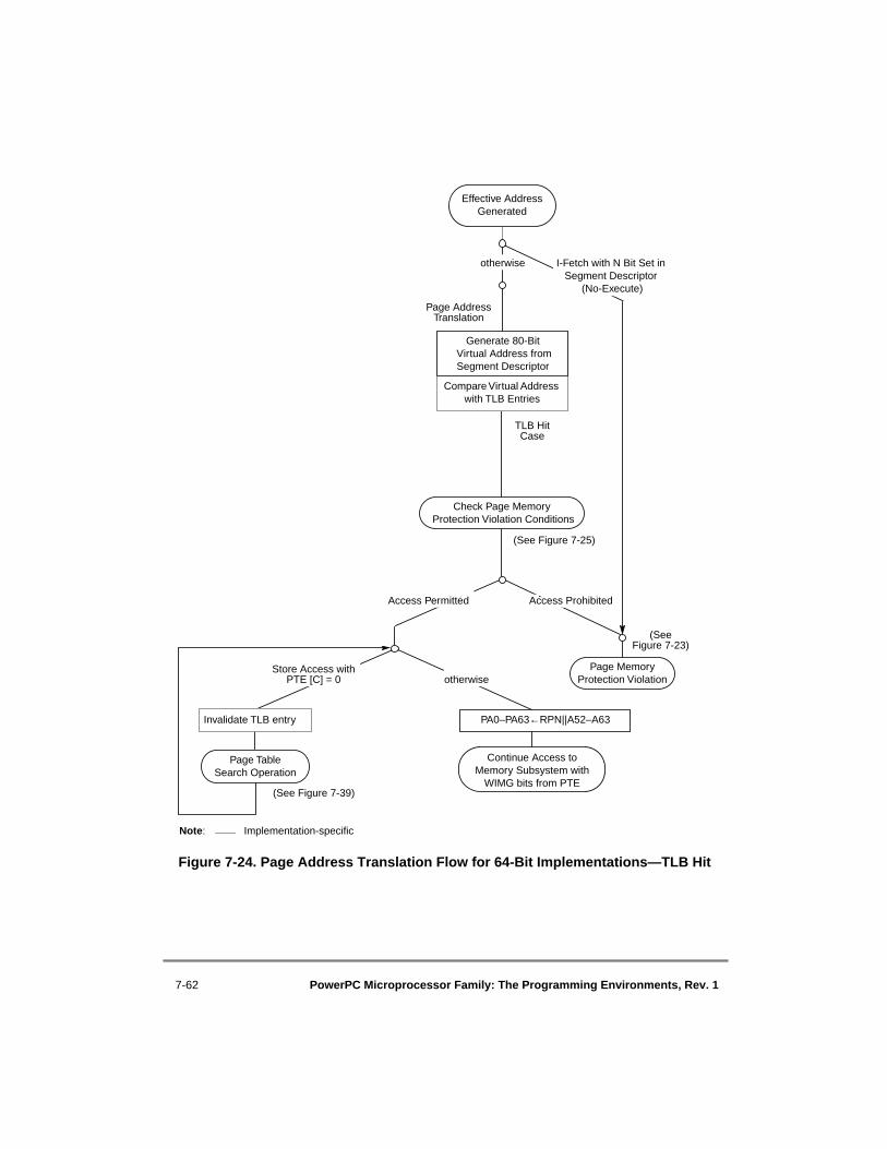
7-62 PowerPC Microprocessor Family: The Programming Environments, Rev. 1
Figure 7-24. Page Address Translation Flow for 64-Bit Implementations—TLB Hit
(See Figure 7-39)
(See Figure 7-25)
TLB Hit Case
Effective AddressGenerated
Compare Virtual Address with TLB Entries
Continue Access to Memory Subsystem with
WIMG bits from PTE
Page TableSearch Operation
PA0–PA63←RPN||A52–A63Invalidate TLB entry
Generate 80-Bit Virtual Address from Segment Descriptor
Page Address Translation
Check Page Memory Protection Violation Conditions
Page Memory Protection Violation
Access ProhibitedAccess Permitted
otherwiseStore Access with
PTE [C] = 0
otherwise
(See Figure 7-23)
I-Fetch with N Bit Set in Segment Descriptor
(No-Execute)
Implementation-specificNote:

Chapter 7. Memory Management 7-63
Figure 7-25. Page Memory Protection Violation Conditions for Page Address Translation
7.6 Hashed Page TablesIf a copy of the PTE corresponding to the VPN for an access is not resident in a TLB(corresponding to a miss in the TLB, provided a TLB is implemented), the processor mustsearch for the PTE in the page tables set up by the operating system in main memory.
The algorithm specified by the architecture for accessing the page tables includes a hashingfunction on some of the virtual address bits. Thus, the addresses for PTEs are allocatedmore evenly within the page tables and the hit rate of the page tables is maximized. Thisalgorithm must be synthesized by the operating system for it to correctly place the pagetable entries in main memory.
If page table search operations are performed automatically by the hardware, they areperformed using physical addresses and as if the memory access attribute bit M = 1(memory coherency enforced in hardware). If the software performs the page table searchoperations, the accesses must be performed in real addressing mode (MSR[DR] = 0); thisadditionally guarantees that M = 1.
This section describes the format of the page tables and the algorithm used to access them.In addition, the constraints imposed on the software in updating the page tables (and otherMMU resources) are described.
Select Key:If MSR[PR] = 0, key = KsIf MSR[PR] = 1, key = Kp
Check Page Memory Protection Violation
Conditions
Access Permitted
otherwise
Read Access with key || PP =
100
Write Access with key || PP = any of:
011100101111
Access Prohibited (See Figure 7-23)

7-64 PowerPC Microprocessor Family: The Programming Environments, Rev. 1
7.6.1 Page Table DefinitionThe hashed page table is a variable-sized data structure that defines the mapping betweenvirtual page numbers and physical page numbers. The page table size is a power of 2, itsstarting address is a multiple of its size, and the table must reside in memory with theWIMG attributes of 0b0010.
The page table contains a number of page table entry groups (PTEGs). For 64-bitimplementations, a PTEG contains eight page table entries (PTEs) of 16 bytes each;therefore, each PTEG is 128 bytes long. For 32-bit implementations, a PTEG contains eightPTEs of eight bytes each; therefore, each PTEG is 64 bytes long. PTEG addresses are entrypoints for table search operations. Figure 7-26 shows two PTEG addresses (PTEGaddr1and PTEGaddr2) where a given PTE may reside.
Figure 7-26. Page Table Definitions
A given PTE can reside in one of two possible PTEGS—one is the primary PTEG and theother is the secondary PTEG. Additionally, a given PTE can reside in any of the PTElocations within an addressed PTEG. Thus, a given PTE may reside in one of 16 possiblelocations within the page table. If a given PTE is not in either the primary or secondaryPTEG, a page table miss occurs, corresponding to a page fault condition.
A table search operation is defined as the search for a PTE within a primary and secondaryPTEG. When a table search operation commences, a primary hashing function is performedon the virtual address. The output of the hashing function is then concatenated with bitsprogrammed into the SDR1 register by the operating system to create the physical address
16 bytes
PTE0 PTE1 PTE7 PTEG0
PTE0 PTE1 PTE7
PTE0 PTE1 PTE7
PTEGn
PTEGaddr1
PTEGaddr2
Page Table
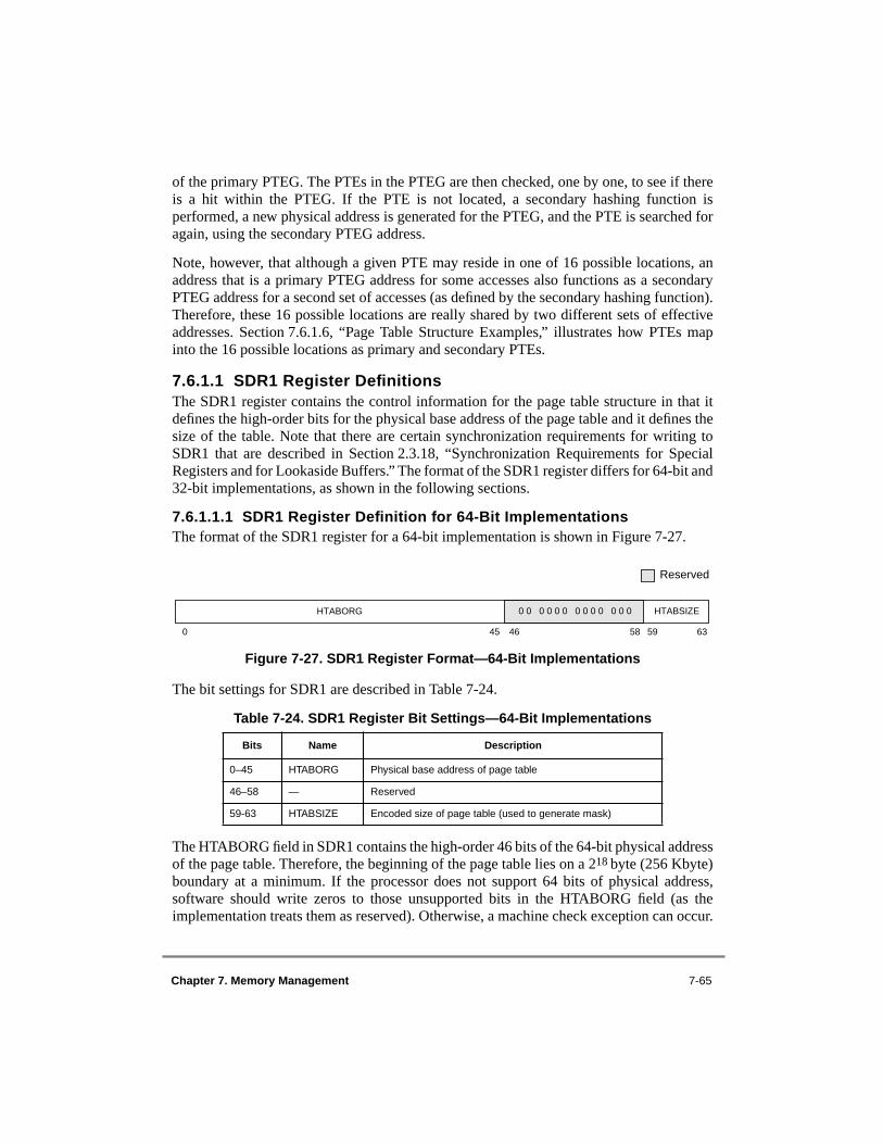
Chapter 7. Memory Management 7-65
of the primary PTEG. The PTEs in the PTEG are then checked, one by one, to see if thereis a hit within the PTEG. If the PTE is not located, a secondary hashing function isperformed, a new physical address is generated for the PTEG, and the PTE is searched foragain, using the secondary PTEG address.
Note, however, that although a given PTE may reside in one of 16 possible locations, anaddress that is a primary PTEG address for some accesses also functions as a secondaryPTEG address for a second set of accesses (as defined by the secondary hashing function).Therefore, these 16 possible locations are really shared by two different sets of effectiveaddresses. Section 7.6.1.6, “Page Table Structure Examples,” illustrates how PTEs mapinto the 16 possible locations as primary and secondary PTEs.
7.6.1.1 SDR1 Register DefinitionsThe SDR1 register contains the control information for the page table structure in that itdefines the high-order bits for the physical base address of the page table and it defines thesize of the table. Note that there are certain synchronization requirements for writing toSDR1 that are described in Section 2.3.18, “Synchronization Requirements for SpecialRegisters and for Lookaside Buffers.” The format of the SDR1 register differs for 64-bit and32-bit implementations, as shown in the following sections.
7.6.1.1.1 SDR1 Register Definition for 64-Bit ImplementationsThe format of the SDR1 register for a 64-bit implementation is shown in Figure 7-27.
Figure 7-27. SDR1 Register Format—64-Bit Implementations
The bit settings for SDR1 are described in Table 7-24.
The HTABORG field in SDR1 contains the high-order 46 bits of the 64-bit physical addressof the page table. Therefore, the beginning of the page table lies on a 218 byte (256 Kbyte)boundary at a minimum. If the processor does not support 64 bits of physical address,software should write zeros to those unsupported bits in the HTABORG field (as theimplementation treats them as reserved). Otherwise, a machine check exception can occur.
Table 7-24. SDR1 Register Bit Settings—64-Bit Implementations
Bits Name Description
0–45 HTABORG Physical base address of page table
46–58 — Reserved
59-63 HTABSIZE Encoded size of page table (used to generate mask)
0 0 0 0 0 0 0 0 0 0 0 0 0 HTABSIZE
Reserved
0 45 46 58 59 63
HTABORG
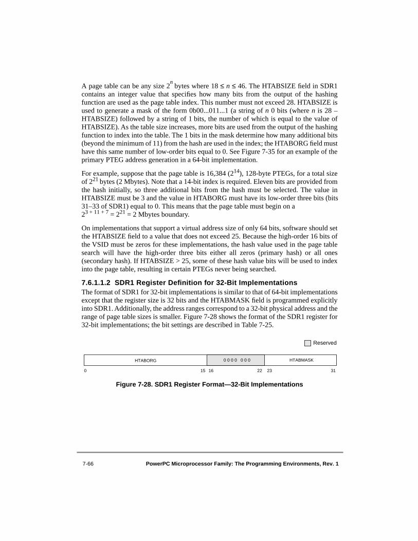
7-66 PowerPC Microprocessor Family: The Programming Environments, Rev. 1
A page table can be any size 2n bytes where 18 ≤ n ≤ 46. The HTABSIZE field in SDR1
contains an integer value that specifies how many bits from the output of the hashingfunction are used as the page table index. This number must not exceed 28. HTABSIZE isused to generate a mask of the form 0b00...011...1 (a string of n 0 bits (where n is 28 –HTABSIZE) followed by a string of 1 bits, the number of which is equal to the value ofHTABSIZE). As the table size increases, more bits are used from the output of the hashingfunction to index into the table. The 1 bits in the mask determine how many additional bits(beyond the minimum of 11) from the hash are used in the index; the HTABORG field musthave this same number of low-order bits equal to 0. See Figure 7-35 for an example of theprimary PTEG address generation in a 64-bit implementation.
For example, suppose that the page table is 16,384 (214), 128-byte PTEGs, for a total sizeof 221 bytes (2 Mbytes). Note that a 14-bit index is required. Eleven bits are provided fromthe hash initially, so three additional bits from the hash must be selected. The value inHTABSIZE must be 3 and the value in HTABORG must have its low-order three bits (bits 31–33 of SDR1) equal to 0. This means that the page table must begin on a 23 + 11 + 7 = 221 = 2 Mbytes boundary.
On implementations that support a virtual address size of only 64 bits, software should setthe HTABSIZE field to a value that does not exceed 25. Because the high-order 16 bits ofthe VSID must be zeros for these implementations, the hash value used in the page tablesearch will have the high-order three bits either all zeros (primary hash) or all ones(secondary hash). If HTABSIZE > 25, some of these hash value bits will be used to indexinto the page table, resulting in certain PTEGs never being searched.
7.6.1.1.2 SDR1 Register Definition for 32-Bit ImplementationsThe format of SDR1 for 32-bit implementations is similar to that of 64-bit implementationsexcept that the register size is 32 bits and the HTABMASK field is programmed explicitlyinto SDR1. Additionally, the address ranges correspond to a 32-bit physical address and therange of page table sizes is smaller. Figure 7-28 shows the format of the SDR1 register for32-bit implementations; the bit settings are described in Table 7-25.
Figure 7-28. SDR1 Register Format—32-Bit Implementations
0 0 0 0 0 0 0 HTABMASK
Reserved
0 15 16 22 23 31
HTABORG

Chapter 7. Memory Management 7-67
The HTABORG field in SDR1 contains the high-order 16 bits of the 32-bit physical addressof the page table. Therefore, the beginning of the page table lies on a 216 byte (64 Kbyte)boundary at a minimum. As with 64-bit implementations, if the processor does not support32 bits of physical address, software should write zeros to those unsupported bits in theHTABORG field (as the implementation treats them as reserved). Otherwise, a machinecheck exception can occur.
A page table can be any size 2n bytes where 16 ≤ n ≤ 25. The HTABMASK field in SDR1
contains a mask value that determines how many bits from the output of the hashingfunction are used as the page table index. This mask must be of the form 0b00...011...1 (astring of 0 bits followed by a string of 1 bits). As the table size increases, more bits are usedfrom the output of the hashing function to index into the table. The 1 bits in HTABMASKdetermine how many additional bits (beyond the minimum of 10) from the hash are used inthe index; the HTABORG field must have the same number of lower-order bits equal to 0as the HTABMASK field has lower-order bits equal to 1.
Example:
Suppose that the page table is 16,384 (214) 128-byte PTEGs, for a total size of 221 bytes(2 Mbytes). A 14-bit index is required. Eleven bits are provided from the hash to start with,so 3 additional bits from the hash must be selected. Thus the value in HTABMASK mustbe 3 and the value in HTABORG must have its low-order 3 bits (SDR1[31–33]) equal to 0.This means that the page table must begin on a 2 <3 + 11 + 7> = 2 21 = 2-Mbyte boundary.
7.6.1.2 Page Table Size The number of entries in the page table directly affects performance because it influencesthe hit ratio in the page table and thus the rate of page fault exception conditions. If the tableis too small, not all virtual pages that have physical page frames assigned may be mappedvia the page table. This can happen if more than 16 entries map to the sameprimary/secondary pair of PTEGs; in this case, many hash collisions may occur.
Table 7-25. SDR1 Register Bit Settings—32-Bit Implementations
Bits Name Description
0–15 HTABORG Physical base address of page table
16–22 — Reserved
23–31 HTABMASK Mask for page table address

7-68 PowerPC Microprocessor Family: The Programming Environments, Rev. 1
7.6.1.2.1 Page Table Sizes for 64-Bit ImplementationsIn 64-bit implementations, the minimum allowable size for a page table is 256 Kbytes (211
PTEGs of 128 bytes each). However, it is recommended that the total number of PTEGs inthe page table be at least half the number of physical page frames to be mapped. Whileavoidance of hash collisions cannot be guaranteed for any size page table, making the pagetable larger than the recommended minimum size reduces the frequency of such collisions,by making the primary PTEGs more sparsely populated, and further reducing the need touse the secondary PTEGs.
Table 7-26 shows example sizes for total main memory. The recommended minimum pagetable sizes for these example memory sizes are then outlined, along with theircorresponding HTABORG and HTABSIZE settings. Note that systems with less than16 Mbytes of main memory may be designed with 64-bit implementations, but theminimum amount of memory that can be used for the page tables is 256 Kbytes in thesecases.
As an example, if the physical memory size is 231 bytes (2 Gbyte), there are 231 – 212
(4 Kbyte page size) = 219 (512 Kbyte) total page frames. If this number of page frames isdivided by 2, the resultant minimum recommended page table size is 218 PTEGs, or225 bytes (32 Mbytes) of memory for the page tables.
Table 7-26. Minimum Recommended Page Table Sizes—64-Bit Implementations
Total Main Memory
Recommended MinimumSettings for Recommended
Minimum
Memory for Page Tables
Number of Mapped Pages (PTEs)
Number of PTEGs
HTABORG (Maskable Bits 18-45)
HTABSIZE (28-Bit Mask)
16 Mbytes (224) 256 Kbytes (218) 214 211 x . . . . xxxx 0 0000(0 . . . . 0000)
32 Mbytes (225) 512 Kbytes (219) 215 212 x . . . . xxx0 0 0001(0 . . . . 0001)
64 Mbytes (226) 1 Mbyte (220) 216 213 x . . . . xx00 0 0010(0 . . . . 0011)
128 Mbytes (227) 2 Mbytes (221) 217 214 x . . . . x000 0 0011(0 . . . . 0111)
256 Mbytes (228) 4 Mbytes (222) 218 215 x . . .x 0000 0 0100(0 . . .0 1111)
.
.
.
.
.
.
.
.
.
.
.
.
.
.
.
.
.
.
251 Bytes 245 Bytes 241 238 x 0 . . . 0000 1 1011(0 1 . . . 1111)
252 Bytes 246 Bytes 242 239 0 . . . . 0000 1 1100(1 . . . .1111)

Chapter 7. Memory Management 7-69
7.6.1.2.2 Page Table Sizes for 32-Bit ImplementationsThe recommended page table sizes in 32-bit implementations are similar to that of 64-bitimplementations, except that the total number of pages mapped for a given page table sizeis larger, because the PTEs are only 8 bytes (instead of 16 bytes) in length. In a 32-bitimplementation, the minimum size for a page table is 64 Kbytes (210 PTEGs of 64 byteseach). However, as with the 64-bit model, it is recommended that the total number ofPTEGs in the page table be at least half the number of physical page frames to be mapped.While avoidance of hash collisions cannot be guaranteed for any size page table, makingthe page table larger than the recommended minimum size reduces the frequency of suchcollisions by making the primary PTEGs more sparsely populated, and further reducing theneed to use the secondary PTEGs.
Table 7-27 shows some example sizes for total main memory in a 32-bit system. Therecommended minimum page table size for these example memory sizes are then outlined,along with their corresponding HTABORG and HTABMASK settings in SDR1. Note thatsystems with less than 8 Mbytes of main memory may be designed with 32-bit processors,but the minimum amount of memory that can be used for the page tables in these cases is64 Kbytes.
As an example, if the physical memory size is 229 bytes (512 Mbyte), then there are229 – 212 (4 Kbyte page size) = 217 (128 Kbyte) total page frames. If this number of pageframes is divided by 2, the resultant minimum recommended page table size is 216 PTEGs,or 222 bytes (4 Mbytes) of memory for the page tables.
Table 7-27. Minimum Recommended Page Table Sizes—32-Bit Implementations
Total Main Memory
Recommended MinimumSettings for Recommended
Minimum
Memory for Page Tables
Number of Mapped
Pages (PTEs)
Number of PTEGs
HTABORG (Maskable Bits 7–15)
HTABMASK
8 Mbytes (223) 64 Kbytes (216) 213 210 x xxxx xxxx 0 0000 0000
16 Mbytes (224) 128 Kbytes (217) 214 211 x xxxx xxx0 0 0000 0001
32 Mbytes (225) 256 Kbytes (218) 215 212 x xxxx xx00 0 0000 0011
64 Mbytes (226) 512 Kbytes (219) 216 213 x xxxx x000 0 0000 0111
128 Mbytes (227) 1 Mbyte (220) 217 214 x xxxx 0000 0 0000 1111
256 Mbytes (228) 2 Mbytes (221) 218 215 x xxx0 0000 0 0001 1111
512 Mbytes (229) 4 Mbytes (222) 219 216 x xx00 0000 0 0011 1111
1 Gbytes (230) 8 Mbytes (223) 220 217 x x000 0000 0 0111 1111
2 Gbytes (231) 16 Mbytes (224) 221 218 x 0000 0000 0 1111 1111
4 Gbytes (232) 32 Mbytes (225) 222 219 0 0000 0000 1 1111 1111
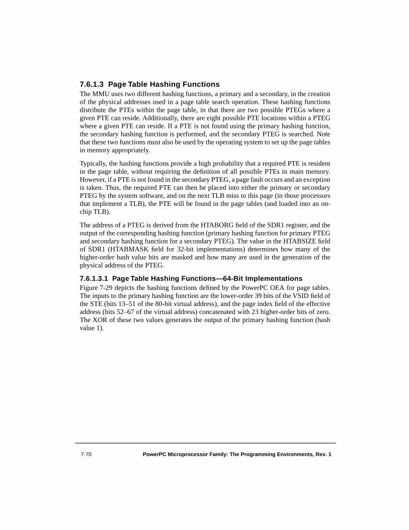
7-70 PowerPC Microprocessor Family: The Programming Environments, Rev. 1
7.6.1.3 Page Table Hashing FunctionsThe MMU uses two different hashing functions, a primary and a secondary, in the creationof the physical addresses used in a page table search operation. These hashing functionsdistribute the PTEs within the page table, in that there are two possible PTEGs where agiven PTE can reside. Additionally, there are eight possible PTE locations within a PTEGwhere a given PTE can reside. If a PTE is not found using the primary hashing function,the secondary hashing function is performed, and the secondary PTEG is searched. Notethat these two functions must also be used by the operating system to set up the page tablesin memory appropriately.
Typically, the hashing functions provide a high probability that a required PTE is residentin the page table, without requiring the definition of all possible PTEs in main memory.However, if a PTE is not found in the secondary PTEG, a page fault occurs and an exceptionis taken. Thus, the required PTE can then be placed into either the primary or secondaryPTEG by the system software, and on the next TLB miss to this page (in those processorsthat implement a TLB), the PTE will be found in the page tables (and loaded into an on-chip TLB).
The address of a PTEG is derived from the HTABORG field of the SDR1 register, and theoutput of the corresponding hashing function (primary hashing function for primary PTEGand secondary hashing function for a secondary PTEG). The value in the HTABSIZE fieldof SDR1 (HTABMASK field for 32-bit implementations) determines how many of thehigher-order hash value bits are masked and how many are used in the generation of thephysical address of the PTEG.
7.6.1.3.1 Page Table Hashing Functions—64-Bit ImplementationsFigure 7-29 depicts the hashing functions defined by the PowerPC OEA for page tables.The inputs to the primary hashing function are the lower-order 39 bits of the VSID field ofthe STE (bits 13–51 of the 80-bit virtual address), and the page index field of the effectiveaddress (bits 52–67 of the virtual address) concatenated with 23 higher-order bits of zero.The XOR of these two values generates the output of the primary hashing function (hashvalue 1).

Chapter 7. Memory Management 7-71
Figure 7-29. Hashing Functions for Page Tables—64-Bit Implementations
When the secondary hashing function is required, the output of the primary hashingfunction is complemented with one’s complement arithmetic, to provide hash value 2.
7.6.1.3.2 Page Table Hashing Functions—32-Bit ImplementationsFigure 7-30 depicts the hashing functions defined by the PowerPC OEA for 32-bitimplementations. The inputs to the primary hashing function are the lower-order 19 bits ofthe VSID field of the selected segment register (bits 5–23 of the 52-bit virtual address), andthe page index field of the effective address (bits 24–39 of the virtual address) concatenatedwith three zero higher-order bits. The XOR of these two values generates the output of theprimary hashing function (hash value 1).
As is the case for 64-bit implementations, when the secondary hashing function is required,the output of the primary hashing function is complemented with one’s complementarithmetic, to provide hash value 2.
Lower-Order 39 Bits of VSID (from Segment Descriptor)
VA13 VA51
52 67
Primary Hash:
XOR
Output of Hashing Function 1
0 27 28 38
=
Secondary Hash:
Hash Value 1
0 38
Hash Value 1
Hash Value 2
One’s Complement Function
0 0 0 . . . . . . 0 0 0(23 Zeros)
Page Index(from Effective Address)
Output of Hashing Function 2
0 27 28 38
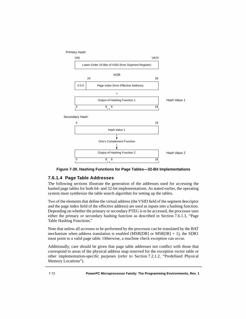
7-72 PowerPC Microprocessor Family: The Programming Environments, Rev. 1
Figure 7-30. Hashing Functions for Page Tables—32-Bit Implementations
7.6.1.4 Page Table AddressesThe following sections illustrate the generation of the addresses used for accessing thehashed page tables for both 64- and 32-bit implementations. As stated earlier, the operatingsystem must synthesize the table search algorithm for setting up the tables.
Two of the elements that define the virtual address (the VSID field of the segment descriptorand the page index field of the effective address) are used as inputs into a hashing function.Depending on whether the primary or secondary PTEG is to be accessed, the processor useseither the primary or secondary hashing function as described in Section 7.6.1.3, “PageTable Hashing Functions.”
Note that unless all accesses to be performed by the processor can be translated by the BATmechanism when address translation is enabled (MSR[DR] or MSR[IR] = 1), the SDR1must point to a valid page table. Otherwise, a machine check exception can occur.
Additionally, care should be given that page table addresses not conflict with those thatcorrespond to areas of the physical address map reserved for the exception vector table orother implementation-specific purposes (refer to Section 7.2.1.2, “Predefined PhysicalMemory Locations”).
Lower-Order 19 Bits of VSID (from Segment Register)
VA5 VA23
24 39
Primary Hash:
XOR
Output of Hashing Function 1
0 8 9 18
=
Secondary Hash:
Hash Value 1
0 18
Output of Hashing Function 2
0 8 9 18
Hash Value 1
Hash Value 2
One’s Complement Function
0 0 0 Page Index (from Effective Address)

Chapter 7. Memory Management 7-73
7.6.1.4.1 Page Table Address Generation for 64-Bit ImplementationsThe base address of the page table is defined by the high-order bits of SDR1[HTABORG].Effectively, bits 18–45 of the PTEG address are derived from the masking of the higher-order bits of the hash value (as defined by SDR1[HTABSIZE]) concatenated with(implemented as an OR function) the high-order bits of SDR1[HTABORG] as defined byHTABSIZE. Bits 46–56 of the PTEG address are the 11 lower-order bits of the hash value,and bits 57–63 of the PTEG address are zero. In the process of searching for a PTE, theprocessor checks up to eight PTEs located in the primary PTEG and up to eight PTEslocated in the secondary PTEG, if required, searching for a match. Figure 7-31 provides agraphical description of the generation of the PTEG addresses for 64-bit implementations.

7-74 PowerPC Microprocessor Family: The Programming Environments, Rev. 1
Figure 7-31. Generation of Addresses for Page Tables—64-Bit Implementations
Virtual Segment ID API Byte Offset(52 Bit) (5 Bit) (12 Bit)
Virtual Page Number (VPN)
Page Table
0 12 13 51 52 56 57 67 68 79
SDR1
xxxx xx . . . . . . 00(46 Bit)
0 17 18 45 46 58 59 63 0 27 28 38
64-Bit Physical Address of Page Table Entry
PTE0
128 Bytes
80-Bit Virtual Address
PTE716 Bytes
64-Bit Physical Address
VSID API 0...0(52 Bit) (5 Bit) (5 Bit)
VH
Physical Page Number (RPN)(52 Bit)
0 51 52 55 57 61 63
WIMG
(18 Bit) (28 Bit) (11 Bit)
RPN Byte Offset(52 Bit) (12 Bit)
(16 Bit)
Hash Function
PTEG0
PTEGn
Page Index (16 Bit)
Mask
0 17 18 45 46 56 57 63
PTEG Select
PP
PTE0 51 52 57 62 63
28 Bits 11 Bits
0 0 0 0 0 0 0
000 0
0 0 0 ... 0 0 0
0 0 . . 0 0(7 Bit)
BaseAddress
Integer Value
AND
Decode
0 27
0 0 0 . . . 011 . . . 11
OR
(23 Bits)
39 Bits
R C
Hash Value(39 Bit)

Chapter 7. Memory Management 7-75
7.6.1.4.2 Page Table Address Generation for 32-Bit ImplementationsFor 32-bit implementations, the base address of the page table is defined by the high-orderbits of SDR1[HTABORG].
Effectively, bits 7–15 of the PTEG address are derived from the masking of the higher-orderbits of the hash value (as defined by SDR1[HTABMASK]) concatenated with(implemented as an OR function) the high-order bits of SDR1[HTABORG] as defined byHTABMASK. Bits 16–25 of the PTEG address are the 10 lower-order bits of the hashvalue, and bits 26–31 of the PTEG address are zero. In the process of searching for a PTE,the processor checks up to eight PTEs located in the primary PTEG and up to eight PTEslocated in the secondary PTEG, if required, searching for a match. Figure 7-32 provides agraphical description of the generation of the PTEG addresses for 32-bit implementations.

7-76 PowerPC Microprocessor Family: The Programming Environments, Rev. 1
Figure 7-32. Generation of Addresses for Page Tables—32-Bit Implementations
Virtual Segment ID API Byte Offset(24 Bit) (6 Bit) (12 Bit)
Virtual Page Number (VPN)
PAGE TABLE
(3 Bit)
0 4 5 23 24 29 30 39 40 51
SDR1
xxxx xx . . . . . . 00 00 . . . . 011 . . .1
0 6 7 15 16 22 23 31 0 8 9 18
32-Bit Physical Address of Page Table Entry
PTE0
64 Bytes
52-Bit Virtual Address
PTE78 Bytes
32-Bit Physical Address
VSID API(24 Bit) (6 Bit)
V H
Physical Page Number (RPN)(20 Bit)
0 19 23 25 29 31
WIMG
AND
OR
(7 Bit) (9 Bit) (10 Bit)
RPN Byte Offset(20 Bit) (12 Bit)
(16 Bit)
Hash Function
Hash Value(19 Bit)
PTEG0
PTEGn
Page Index (16 Bit)
Mask
0 6 7 15 16 25 26 31
PTEG Select
PP
PTE0 1 24 25 26 31
9 Bits 10 Bits
0 0 0 0 0 0 0
000 0
0 0 0
0 0 0 0 0 0(6 Bit)
BaseAddress
CR

Chapter 7. Memory Management 7-77
7.6.1.5 Page Table Structure SummaryIn the process of searching for a PTE, the processor interprets the values read from memoryas described in Section 7.5.2.2, “Page Table Entry (PTE) Definitions.” The VSID and theabbreviated page index (API) fields of the virtual address of the access are compared tothose same fields of the PTEs in memory. In addition, the valid (V) bit and the hashingfunction (H) bit are also checked. For a hit to occur, the V bit of the PTE in memory mustbe set. If the fields match and the entry is valid, the PTE is considered a hit if the H bit isset as follows:
• If this is the primary PTEG, H = 0• If this is the secondary PTEG, H = 1
The physical address of the PTE(s) to be checked is derived as shown in Figure 7-31 andFigure 7-32, and the generated address is the address of a group of eight PTEs (a PTEG).During a table search operation, the processor compares up to 16 PTEs: PTE0–PTE7 of theprimary PTEG (defined by the primary hashing function) and PTE0–PTE7 of the secondaryPTEG (defined by the secondary hashing function).
If the VSID and API fields do not match (or if V or H are not set appropriately) for any ofthese PTEs, a page fault occurs and an exception is taken. Thus, if a valid PTE is located inthe page tables, the page is considered resident; if no matching (and valid) PTE is found foran access, the page in question is interpreted as nonresident (page fault) and the operatingsystem must load the page into main memory and update the PTE accordingly.
The architecture does not specify the order in which the PTEs are checked. Note that formaximum performance however, PTEs should be allocated by the operating system firstbeginning with the PTE0 location within the primary PTEG, then PTE1, and so on. If morethan eight PTEs are required within the address space that defines a PTEG address, thesecondary PTEG can be used (again, allocation of PTE0 of the secondary PTEG first, andso on is recommended). Additionally, it may be desirable to place the PTEs that will requiremost frequent access at the beginning of a PTEG and reserve the PTEs in the secondaryPTEG for the least frequently accessed PTEs.
The architecture also allows for multiple matching entries to be found within a table searchoperation. Multiple matching PTEs are allowed if they meet the match criteria describedabove, as well as have identical RPN, WIMG, and PP values, allowing for differences in theR and C bits. In this case, one of the matching PTEs is used and the R and C bits are updatedaccording to this PTE. In the case that multiple PTEs are found that meet the match criteriabut differ in the RPN, WIMG or PP fields, the translation is undefined and the resultant Rand C bits in the matching entries are also undefined.
Note that multiple matching entries can also differ in the setting of the H bit, but the H bitmust be set according to whether the PTE was located in the primary or secondary PTEG,as described above.
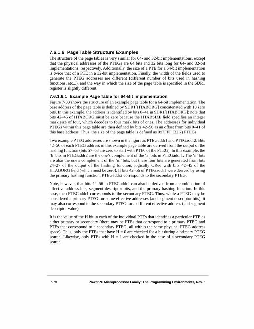
7-78 PowerPC Microprocessor Family: The Programming Environments, Rev. 1
7.6.1.6 Page Table Structure ExamplesThe structure of the page tables is very similar for 64- and 32-bit implementations, exceptthat the physical addresses of the PTEGs are 64 bits and 32 bits long for 64- and 32-bitimplementations, respectively. Additionally, the size of a PTE for a 64-bit implementationis twice that of a PTE in a 32-bit implementation. Finally, the width of the fields used togenerate the PTEG addresses are different (different number of bits used in hashingfunctions, etc...), and the way in which the size of the page table is specified in the SDR1register is slightly different.
7.6.1.6.1 Example Page Table for 64-Bit ImplementationFigure 7-33 shows the structure of an example page table for a 64-bit implementation. Thebase address of the page table is defined by SDR1[HTABORG] concatenated with 18 zerobits. In this example, the address is identified by bits 0–41 in SDR1[HTABORG]; note thatbits 42–45 of HTABORG must be zero because the HTABSIZE field specifies an integermask size of four, which decodes to four mask bits of ones. The addresses for individualPTEGs within this page table are then defined by bits 42–56 as an offset from bits 0–41 ofthis base address. Thus, the size of the page table is defined as 0x7FFF (32K) PTEGs.
Two example PTEG addresses are shown in the figure as PTEGaddr1 and PTEGaddr2. Bits42–56 of each PTEG address in this example page table are derived from the output of thehashing function (bits 57–63 are zero to start with PTE0 of the PTEG). In this example, the‘b’ bits in PTEGaddr2 are the one’s complement of the ‘a’ bits in PTEGaddr1. The ‘n’ bitsare also the one’s complement of the ‘m’ bits, but these four bits are generated from bits24–27 of the output of the hashing function, logically ORed with bits 42–45 of theHTABORG field (which must be zero). If bits 42–56 of PTEGaddr1 were derived by usingthe primary hashing function, PTEGaddr2 corresponds to the secondary PTEG.
Note, however, that bits 42–56 in PTEGaddr2 can also be derived from a combination ofeffective address bits, segment descriptor bits, and the primary hashing function. In thiscase, then PTEGaddr1 corresponds to the secondary PTEG. Thus, while a PTEG may beconsidered a primary PTEG for some effective addresses (and segment descriptor bits), itmay also correspond to the secondary PTEG for a different effective address (and segmentdescriptor value).
It is the value of the H bit in each of the individual PTEs that identifies a particular PTE aseither primary or secondary (there may be PTEs that correspond to a primary PTEG andPTEs that correspond to a secondary PTEG, all within the same physical PTEG addressspace). Thus, only the PTEs that have H = 0 are checked for a hit during a primary PTEGsearch. Likewise, only PTEs with H = 1 are checked in the case of a secondary PTEGsearch.

Chapter 7. Memory Management 7-79
Figure 7-33. Example Page Table Structure—64-Bit Implementations
7.6.1.6.2 Example Page Table for 32-Bit ImplementationFigure 7-34 shows the structure of an example page table for a 32-bit implementation. Thebase address of the page table is defined by SDR1[HTABORG] concatenated with 16 zerobits. In this example, the address is identified by bits 0–13 in SDR1[HTABORG]; note thatbits 14 and 15 of HTABORG must be zero because the lower-order two bits ofHTABMASK are ones. The addresses for individual PTEGs within this page table are then
0 42 56 63
PTE0 PTE1 PTE7 PTEG0
PTE0 PTE1 PTE7
PTE0 PTE1 PTE7
PTEG7FFF
PTEGaddr1
PTEGaddr2
Page Table
Example:
Given: SDR1
0000 0000 1111 0000 0001 1000 0000 0000 1010 0110 0000 0000 0000 0000 0000 0100
0 45 46 58 59 63
$00F0 1800 A600 0000
PTEGaddr1 =
0000 0000 1111 0000 0001 1000 0000 0000 1010 0110 00mm mmaa aaaa aaaa a000 0000
PTEGaddr2 =
HTABORG
HTABSIZE
Base Address (0–41)
decode
28-Bit Mask (0...0 1111)
0000 0000 1111 0000 0001 1000 0000 0000 1010 0110 00nn nnbb bbbb bbbb b000 0000
0 42 56 63

7-80 PowerPC Microprocessor Family: The Programming Environments, Rev. 1
defined by bits 14–25 as an offset from bits 0–13 of this base address. Thus, the size of thepage table is defined as 4096 PTEGs.
Figure 7-34. Example Page Table Structure—32-Bit Implementations
Two example PTEG addresses are shown in the figure as PTEGaddr1 and PTEGaddr2. Bits14–25 of each PTEG address in this example page table are derived from the output of thehashing function (bits 26–31 are zero to start with PTE0 of the PTEG). In this example, the‘b’ bits in PTEGaddr2 are the one’s complement of the ‘a’ bits in PTEGaddr1. The ‘n’ bitsare also the one’s complement of the ‘m’ bits, but these two bits are generated from bits 7–8of the output of the hashing function, logically ORed with bits 14–15 of the HTABORGfield (which must be zero). If bits 14–25 of PTEGaddr1 were derived by using the primaryhashing function, then PTEGaddr2 corresponds to the secondary PTEG.
PTE0 PTE1 PTE7 PTEG0
PTE0 PTE1 PTE7
PTE0 PTE1 PTE7
PTEG4095
PTEGaddr1
PTEGaddr2
Page Table
Example:
Given: SDR1 1010 0110 0000 0000 0000 0000 0000 0011
0 15 23 31
Base Address
$A600 0000
PTEGaddr1 = 1010 0110 0000 00mm aaaa aaaa aa00 0000
0 14 25 31
PTEGaddr2 = 1010 0110 0000 00nn bbbb bbbb bb00 0000
0 14 25 31
HTABORG HTABMASK

Chapter 7. Memory Management 7-81
Note, however, that bits 14–25 in PTEGaddr2 can also be derived from a combination ofeffective address bits, segment register bits, and the primary hashing function. In this case,then PTEGaddr1 corresponds to the secondary PTEG. Thus, while a PTEG may beconsidered a primary PTEG for some effective addresses (and segment register bits), it mayalso correspond to the secondary PTEG for a different effective address (and segmentregister value).
It is the value of the H bit in each of the individual PTEs that identifies a particular PTE aseither primary or secondary (there may be PTEs that correspond to a primary PTEG andPTEs that correspond to a secondary PTEG, all within the same physical PTEG addressspace). Thus, only the PTEs that have H = 0 are checked for a hit during a primary PTEGsearch. Likewise, only PTEs with H = 1 are checked in the case of a secondary PTEGsearch.
7.6.1.7 PTEG Address Mapping ExamplesThis section contains two examples of an effective address and how its address translation(the PTE) maps into the primary PTEG in physical memory. The examples illustrate howthe processor generates PTEG addresses for a table search operation; this is also thealgorithm that must be used by the operating system in creating page tables. There is oneexample for a 64-bit implementation and a second example for a 32-bit implementation.
7.6.1.7.1 PTEG Address Mapping Example—64-Bit ImplementationIn the example shown in Figure 7-35, the value in SDR1 defines a page table at address0x0F05_8400_0F00_0000 that contains 217 PTEGs. The highest order 36 bits of theeffective address uniquely map to a segment descriptor. The segment descriptor is thenlocated and the contents of the segment descriptor are used along with bits 36–63 of theeffective address to create the 80-bit virtual address.
To generate the address of the primary PTEG, bits 13–51, and bits 52–67 of the virtualaddress are then used as inputs into the primary hashing function (XOR) to generate hashvalue 1. The low-order 17 bits of hash value 1 are then concatenated with the high-order 40bits of HTABORG and with seven low-order 0 bits, defining the address of the primaryPTEG (0x0F05_8400_0F3F_F300). The ANDing of the 28 high-order bits of hash value 1with the mask (defined by the HTABSIZE field) and the ORing with bits 18–45 ofHTABORG are implicitly shown in the figure. The ANDing with the mask selects sixadditional bits of hash value 1 to be used (in addition to the 11 prescribed bits) producinga total of 17 bits of hash value 1 bits to be used. The ORing causes those selected six bitsof hash value 1 to comprise bits 40–45 of the PTEG address (as bits 40–45 of HTABORGshould be zero).
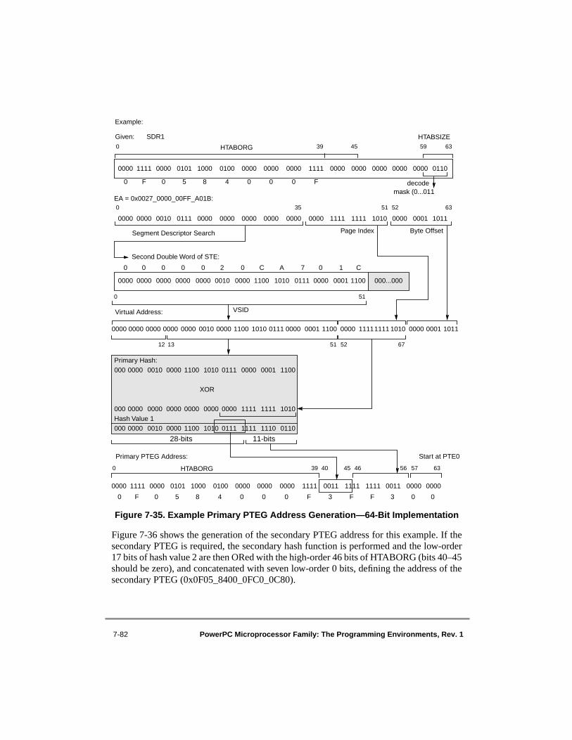
7-82 PowerPC Microprocessor Family: The Programming Environments, Rev. 1
Figure 7-35. Example Primary PTEG Address Generation—64-Bit Implementation
Figure 7-36 shows the generation of the secondary PTEG address for this example. If thesecondary PTEG is required, the secondary hash function is performed and the low-order17 bits of hash value 2 are then ORed with the high-order 46 bits of HTABORG (bits 40–45should be zero), and concatenated with seven low-order 0 bits, defining the address of thesecondary PTEG (0x0F05_8400_0FC0_0C80).
Byte Offset
0 39 40 45 46 56 57 63
Page Index
Example:
Given: SDR1
0000 1111 0000 0101 1000 0100 0000 0000 0000 1111 0000 0000 0000 0000 0000 0110
0 39 45 59 63HTABORG
HTABSIZE
EA = 0x0027_0000_00FF_A01B:
Second Double Word of STE:
Segment Descriptor Search
0 0 0 0 0 2 0 C A 7 0 1 C
0 51
12 13 51 52 67
Virtual Address: VSID
Primary Hash:000 0000 0010 0000 1100 1010 0111 0000 0001 1100
XOR
000 0000 0000 0000 0000 0000 0000 1111 1111 1010Hash Value 1000 0000 0010 0000 1100 1010 0111 1111 1110 0110
28-bits 11-bits
0000 1111 0000 0101 1000 0100 0000 0000 0000 1111 0011 1111 1111 0011 0000 0000
0 F 0 5 8 4 0 0 0 F 3 F F 3 0 0
Primary PTEG Address: Start at PTE0
HTABORG
0 35 51 52 63
0000 0000 0010 0111 0000 0000 0000 0000 0000 0000 1111 1111 1010 0000 0001 1011
0 F 0 5 8 4 0 0 0 F
0000 0000 0000 0000 0000 0010 0000 1100 1010 0111 0000 0001 1100 000...000
0000 0000 0000 0000 0000 0010 0000 1100 1010 0111 0000 0001 1100 0000 11111111 1010 0000 0001 1011
mask (0...011 decode
Chapter 7. Memory Management 7-83
As described in Figure 7-31, the 11 low-order bits of the page index field are always usedin the generation of a PTEG address (through the hashing function). This is why only the5-bit abbreviated page index (API) is defined for a PTE (the entire page index field does notneed to be checked). For a given effective address, the low-order 11 bits of the page index(at least) contribute to the PTEG address (both primary and secondary) where thecorresponding PTE may reside in memory. Therefore, if the high-order 5 bits (the API field)of the page index match with the API field of a PTE within the specified PTEG, the PTEmapping is guaranteed to be the unique PTE required.
Figure 7-36. Example Secondary PTEG Address Generation—64-Bit Implementation
Note that a given PTEG address does not map back to a unique effective address. Not onlycan a given PTEG be considered both a primary and a secondary PTEG (as described inSection 7.6.1.6, “Page Table Structure Examples”), but if the mask defined has four 1 bitsor less (not the case shown in the example in the figure), some bits of the page index fieldof the virtual address are not used to generate the PTEG address. Therefore, anycombination of these unused bits will map to the same pair of PTEG addresses. (However,these bits are part of the API and are therefore compared for each PTE within the PTEG to
Hash Value 2:
Secondary PTEG Address:
0000 1111 0000 0101 1000 0100 0000 0000 0000 1111 1100 0000 0000 1100 1000 0000
0x 0 F 0 5 8 4 0 0 0 F C 0 0 C 8 0
28 Bits11 Bits
1) First compare 8 PTEs at 0x0F05_8400_0F3F_F300
2) Then compare 8 PTEsat 0x0F05_8400_0FC0_0C80,
if necessary
HTABORG
0x0F05_8400_0F00_0000 PTEG0
PTEG
PTEG
PTEG
PTE0 PTE7
PTE0 PTE7
One’s Complement
Secondary Hash:
000 0000 0010 0000 1100 1010 0111 1111 1110 0110Hash Value 1:
Start at PTE0
000 0000 0010 0000 1100 1010 0111 1111 1110 0110
111 1111 1101 1111 0011 0101 1000 0000 0001 1001
0x3F_F300
0xC0_0C80
0xFF_FF80
635646 570 3940 45

7-84 PowerPC Microprocessor Family: The Programming Environments, Rev. 1
determine if there is a hit.) Furthermore, an effective address can select a different segmentdescriptor with a different value such that the output of the primary (or secondary) hashingfunction happens to equal the hash values shown in the example. Thus, these effectiveaddresses would also map to the same PTEG addresses shown.
7.6.1.7.2 PTEG Address Mapping Example—32-Bit ImplementationFigure 7-37 shows an example of PTEG address generation for a 32-bit implementation. Inthe example, the value in SDR1 defines a page table at address 0x0F98_0000 that contains8192 PTEGs. The example effective address selects segment register 0 (SR0) with thehighest order four bits. The contents of SR0 are then used along with bits 4–31 of theeffective address to create the 52-bit virtual address.
To generate the address of the primary PTEG, bits 5–23, and bits 24–39 of the virtualaddress are then used as inputs into the primary hashing function (XOR) to generate hashvalue 1. The low-order 13 bits of hash value 1 are then concatenated with the high-order 16bits of HTABORG and with six low-order 0 bits, defining the address of the primary PTEG(0x0F9F_F980). The ANDing of the nine high-order bits of hash value 1 with the value inthe HTABMASK field and the ORing with bits 7–15 of HTABORG are implicitly shownin the figure. The ANDing with the mask selects three additional bits of hash value 1 to beused (in addition to the 10 prescribed bits) producing a total of 13 bits of hash value 1 bitsto be used. The ORing causes those selected three bits of hash value 1 to comprise bits13–15 of the PTEG address (as bits 13–15 of HTABORG should be zero).
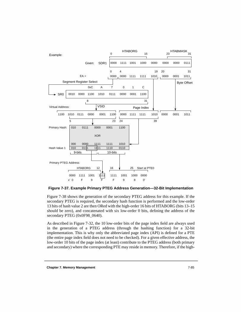
Chapter 7. Memory Management 7-85
Figure 7-37. Example Primary PTEG Address Generation—32-Bit Implementation
Figure 7-38 shows the generation of the secondary PTEG address for this example. If thesecondary PTEG is required, the secondary hash function is performed and the low-order13 bits of hash value 2 are then ORed with the high-order 16 bits of HTABORG (bits 13–15should be zero), and concatenated with six low-order 0 bits, defining the address of thesecondary PTEG (0x0F98_0640).
As described in Figure 7-32, the 10 low-order bits of the page index field are always usedin the generation of a PTEG address (through the hashing function) for a 32-bitimplementation. This is why only the abbreviated page index (API) is defined for a PTE(the entire page index field does not need to be checked). For a given effective address, thelow-order 10 bits of the page index (at least) contribute to the PTEG address (both primaryand secondary) where the corresponding PTE may reside in memory. Therefore, if the high-
Example:
Given: SDR1 0000 1111 1001 1000 0000 0000 0000 0111
0 15 23 31HTABORG HTABMASK
0000 0000 1111 1111 1010 0000 0001 1011
0 4 19 20 31
EA =
SR0
Segment Register Select
0010 0000 1100 1010 0111 0000 0001 1100
0xC A 7 0 1 C
8 31
1100 1010 0111 0000 0001 1100 0000 1111 1111 1010 0000 0001 1011
5 23 24 39
Virtual Address:
Byte Offset
Page IndexVSID
Primary Hash: 010 0111 0000 0001 1100
XOR
000 0000 1111 1111 1010Hash Value 1 010 0111 1111 1110 0110
9-bits 10-bits
0000 1111 1001 1111 1111 1001 1000 0000
x’ 0 F 9 F F 9 8 0’
Primary PTEG Address:
Start at PTE0HTABORG 12 16 25

7-86 PowerPC Microprocessor Family: The Programming Environments, Rev. 1
order 6 bits (the API field as defined for 32-bit implementations) of the page index matchwith the API field of a PTE within the specified PTEG, the PTE mapping is guaranteed tobe the unique PTE required.
Figure 7-38. Example Secondary PTEG Address Generation—32-Bit Implementations
Note that a given PTEG address does not map back to a unique effective address. Not onlycan a given PTEG be considered both a primary and a secondary PTEG (as described inSection 7.6.1.6, “Page Table Structure Examples”), but in this example, bits 24–26 of thepage index field of the virtual address are not used to generate the PTEG address. Therefore,any of the eight combinations of these bits will map to the same primary PTEG address.(However, these bits are part of the API and are therefore compared for each PTE withinthe PTEG to determine if there is a hit.) Furthermore, an effective address can select adifferent segment register with a different value such that the output of the primary (orsecondary) hashing function happens to equal the hash values shown in the example. Thus,these effective addresses would also map to the same PTEG addresses shown.
Hash Value 2: 101 1000 0000 0001 1001
Secondary PTEG Address:
0000 1111 1001 1000 0000 0110 0100 0000
0x 0 F 9 8 0 6 4 0
9 Bits 10 Bits
1) First compare 8 PTEs at 0x0F9F_F980
2) Then compare 8 PTEsat 0x0F98_0640,
if necessary
HTABORG
0x0F98_0000
0x0F98_0640
0x0F9F_F980
PTEG0
PTEG25
PTEG8166
PTEG8191
010 0111 1111 1110 0110
One’s Complement
Secondary Hash:
010 0111 1111 1110 0110Hash Value 1:
Start at PTE0
PTE0 PTE7
PTE0 PTE7
13 16 25
Chapter 7. Memory Management 7-87
7.6.2 Page Table Search OperationThe table search process performed by a PowerPC processor in the search of a PTE variesslightly for 64- and 32-bit implementations. The main differences are the address rangesand PTE formats specified.
7.6.2.1 Page Table Search Operation for 64-Bit ImplementationsAn outline of the page table search process performed by a 64-bit implementation is asfollows:
1. The 64-bit physical addresses of the primary and secondary PTEGs are generated as described in Section 7.6.1.4.1, “Page Table Address Generation for 64-Bit Implementations.”
2. As many as 16 PTEs (from the primary and secondary PTEGs) are read from memory (the architecture does not specify the order of these reads, allowing multiple reads to occur in parallel). PTE reads occur with an implied WIM memory/cache mode control bit setting of 0b001. Therefore, they are considered cacheable.
3. The PTEs in the selected PTEGs are tested for a match with the virtual page number (VPN) of the access. The VPN is the VSID concatenated with the page index field of the virtual address. For a match to occur, the following must be true:
— PTE[H] = 0 for primary PTEG; PTE[H] = 1 for secondary PTEG— PTE[V] = 1— PTE[VSID] = VA[0-51]— PTE[API] = VA[52-56]
4. If a match is not found within the eight PTEs of the primary PTEG and the eight PTEs of the secondary PTEG, an exception is generated as described in step 8. If a match (or multiple matches) is found, the table search process continues.
5. If multiple matches are found, all of the following must be true:
— PTE[RPN] is equal for all matching entries— PTE[WIMG] is equal for all matching entries— PTE[PP] is equal for all matching entries
6. If one of the fields in step 5 does not match, the translation is undefined, and R and C bit of matching entries are undefined. Otherwise, the R and C bits are updated based on one of the matching entries.
7. A copy of the PTE is written into the on-chip TLB (if implemented) and the R bit is updated in the PTE in memory (if necessary). If there is no memory protection violation, the C bit is also updated in memory (if necessary) and the table search is complete.
8. If a match is not found within the primary or secondary PTEG, the search fails, and a page fault exception condition occurs (either an ISI or DSI exception).
7-88 PowerPC Microprocessor Family: The Programming Environments, Rev. 1
Reads from memory for page table search operations are performed as if the WIMG bitsettings were 0b0010 (that is, as unguarded cacheable operations in which coherency isrequired).
7.6.2.2 Page Table Search Operation for 32-Bit ImplementationsAn outline of the page table search process performed by a 32-bit implementation is asfollows:
1. The 32-bit physical addresses of the primary and secondary PTEGs are generated as described in Section 7.6.1.4.2, “Page Table Address Generation for 32-Bit Implementations.”
2. As many as 16 PTEs (from the primary and secondary PTEGs) are read from memory (the architecture does not specify the order of these reads, allowing multiple reads to occur in parallel). PTE reads occur with an implied WIM memory/cache mode control bit setting of 0b001. Therefore, they are considered cacheable.
3. The PTEs in the selected PTEGs are tested for a match with the virtual page number (VPN) of the access. The VPN is the VSID concatenated with the page index field of the virtual address. For a match to occur, the following must be true:
— PTE[H] = 0 for primary PTEG; PTE[H] = 1 for secondary PTEG— PTE[V] = 1— PTE[VSID] = VA[0–23]— PTE[API] = VA[24–29]
4. If a match is not found within the eight PTEs of the primary PTEG and the eight PTEs of the secondary PTEG, an exception is generated as described in step 8. If a match (or multiple matches) is found, the table search process continues.
5. If multiple matches are found, all of the following must be true:
— PTE[RPN] is equal for all matching entries— PTE[WIMG] is equal for all matching entries— PTE[PP] is equal for all matching entries
6. If one of the fields in step 5 does not match, the translation is undefined, and R and C bit of matching entries are undefined. Otherwise, the R and C bits are updated based on one of the matching entries.
7. A copy of the PTE is written into the on-chip TLB (if implemented) and the R bit is updated in the PTE in memory (if necessary). If there is no memory protection violation, the C bit is also updated in memory (if necessary) and the table search is complete.
8. If a match is not found within the primary or secondary PTEG, the search fails, and a page fault exception condition occurs (either an ISI or DSI exception).
Chapter 7. Memory Management 7-89
Reads from memory for page table search operations are performed as if the WIMG bitsettings were 0b0010 (that is, as unguarded cacheable operations in which coherency isrequired).
7.6.2.3 Flow for Page Table Search OperationFigure 7-39 provides a detailed flow diagram of a page table search operation. Note that thereferences to TLBs are shown as optional because TLBs are not required; if they do exist,the specifics of how they are maintained are implementation-specific. Also, Figure 7-39shows only a few cases of R-bit and C-bit updates. For a complete list of the R- and C-bitupdates dictated by the architecture, refer to Table 7-20.

7-90 PowerPC Microprocessor Family: The Programming Environments, Rev. 1
Figure 7-39. Page Table Search Flow
otherwise
otherwise
Update PTE[R](if required)
Generate Primary and Secondary PTEG Addresses
Page Table Search
Adjust PA to read more PTE(s)
Fetch PTE(s)from Physical Address(es)
PTE [VSID, API, V] = Seg Desc [VSID], EA[API], 1PTE [H] = 0 (Primary PTEG) orPTE [H] = 1 (Secondary PTEG)
Translation Undefined
Write PTE into TLB
Check Memory Protection Violation Conditions
otherwise
R, C bits for matching PTEs also undefined
DSI ExceptionISI Exception
SRR1[33*] ← 1 DSISR[1] ← 1
Data AccessInstruction Access
AccessPermitted
AccessProhibited
Page Table Search Complete
otherwise Store operation with PTE[C] = 0
Page Memory Protection Violation
TLB[PTE[C]] ← 1
Page Table Search Complete
PTE[C] ← 1(update PTE[C] in memory)
PTE(RPN, WIMG, PP)equal for all matching PTEs
All 16 PTEs checked
(See Figure 7-25)
(See Figure 7-23)
Page Fault
Notes:*Subtract 32 from bit number for bit setting in 32-bit implementations
Implementation-specific

Chapter 7. Memory Management 7-91
7.6.3 Page Table UpdatesThis section describes the requirements on the software when updating page tables inmemory via some pseudocode examples. Multiprocessor systems must follow the rulesdescribed in this section so that all processors operate with a consistent set of page tables.Even single processor systems must follow certain rules, because software changes must besynchronized with the other instructions in execution and with automatic updates that maybe made by the hardware (referenced and changed bit updates). Updates to the tablesinclude the following operations:
• Adding a PTE• Modifying a PTE, including modifying the R and C bits of a PTE• Deleting a PTE
PTEs must be locked on multiprocessor systems. Access to PTEs must be appropriatelysynchronized by software locking of (that is, guaranteeing exclusive access to) PTEs orPTEGs if more than one processor can modify the table at that time. In the examples below,software locks should be performed to provide exclusive access to the PTE being updated.However, the architecture does not dictate the specific protocol to be used for locking (forexample, a single lock, a lock per PTEG, or a lock per PTE can be used). See Appendix E,“Synchronization Programming Examples,” for more information about the use of thereservation instructions (such as the lwarx and stwcx. instructions) to perform softwarelocking.
When TLBs are implemented they are defined as noncoherent caches of the page tables.TLB entries must be invalidated explicitly with the TLB invalidate entry instruction (tlbie)whenever the corresponding PTE is modified. In a multiprocessor system, the tlbieinstruction must be controlled by software locking, so that the tlbie is issued on only oneprocessor at a time.
The PowerPC OEA defines the tlbsync instruction that ensures that TLB invalidateoperations executed by this processor have caused all appropriate actions in otherprocessors. In a system that contains multiple processors, the tlbsync functionality must beused in order to ensure proper synchronization with the other PowerPC processors. Notethat a sync instruction must also follow the tlbsync to ensure that the tlbsync hascompleted execution on this processor.
On single processor systems, PTEs need not be locked and the eieio instructions (inbetween the tlbie and tlbsync instructions) and the tlbsync instructions themselves are notrequired. The sync instructions shown are required even for single processor systems (toensure that all previous changes to the page tables and all preceding tlbie instructions havecompleted).
Any processor, including the processor modifying the page table, may access the page tableat any time in an attempt to reload a TLB entry. An inconsistent PTE must neveraccidentally become visible (if V = 1); thus, there must be synchronization betweenmodifications to the valid bit and any other modifications (to avoid corrupted data).
7-92 PowerPC Microprocessor Family: The Programming Environments, Rev. 1
In the pseudocode examples that follow, changes made to a PTE or STE shown as a singleline in the example is assumed to be performed with an atomic store instruction.Appropriate modifications must be made to these examples if this assumption is notsatisfied (for example, if a store double-word operation on a 64-bit implementation isperformed with two store word instructions).
Updates of R and C bits by the processor are not synchronized with the accesses that causethe updates. When modifying the low-order half of a PTE, software must take care to avoidoverwriting a processor update of these bits and to avoid having the value written by a storeinstruction overwritten by a processor update. The processor does not alter any other fieldsof the PTE.
Explicitly altering certain MSR bits (using the mtmsrd instruction), or explicitly alteringSTEs, PTEs, or certain system registers, may have the side effect of changing the effectiveor physical addresses from which the current instruction stream is being fetched. This kindof side effect is defined as an implicit branch. For example, an mtmsrd instruction maychange the value of MSR[SF], changing the effective addresses from which the currentinstruction stream is being fetched, causing an implicit branch. Implicit branches are notsupported and an attempt to perform one causes boundedly-undefined results. Therefore,PTEs and STEs must not be changed in a manner that causes an implicit branch.Section 2.3.18, “Synchronization Requirements for Special Registers and for LookasideBuffers,” lists the possible implicit branch conditions that can occur when system registersand MSR bits are changed.
For a complete list of the synchronization requirements for executing the MMUinstructions, see Section 2.3.18, “Synchronization Requirements for Special Registers andfor Lookaside Buffers.”
The following examples show the required sequence of operations. However, otherinstructions may be interleaved within the sequences shown.
7.6.3.1 Adding a Page Table EntryAdding a page table entry requires only a lock on the PTE in a multiprocessor system. Thefirst bytes in the PTE are then written (this example assumes the old valid bit was cleared),the eieio instruction orders the update, and then the second update can be made. A syncinstruction ensures that the updates have been made to memory.
lock(PTE)PTE[RPN,R,C,WIMG,PP] ← new valueseieio /* order 1st PTE update befor 2ndPTE[VSID,H,API,V] ← new values (V = 1)sync /* ensure updates completedunlock(PTE)

Chapter 7. Memory Management 7-93
7.6.3.2 Modifying a Page Table EntryThis section describes several scenarios for modifying a PTE.
7.6.3.2.1 General CaseConsider the general case where a currently-valid PTE must be changed. To do this, thePTE must be locked, marked invalid, updated, invalidated from the TLB, marked validagain, and unlocked. The sync instruction must be used at appropriate times to wait formodifications to complete.
Note that the tlbsync and the sync instruction that follows it are only required if softwareconsistency must be maintained with other PowerPC processors in a multiprocessor system(and the software is to be used in a multiprocessor environment).
lock(PTE)PTE[V] ← 0 /* (other fields don’t matter)sync /* ensure update completedPTE[RPN,R,C,WIMG,PP] ← new valuestlbie(old_EA) /*invalidate old translationeieio /* order tlbie before tlbsync and order 2nd PTE update before 3rdPTE[VSID,H,API, V] ← new values (V = 1)tlbsync /* ensure tlbie completed on all processorssync /* ensure tlbsync and last update completedunlock(PTE)
7.6.3.2.2 Clearing the Referenced (R) BitWhen the PTE is modified only to clear the R bit to 0, a much simpler algorithm sufficesbecause the R bit need not be maintained exactly.
lock(PTE)oldR ←PTE[R] /*get old Rif oldR = 1, then
PTE[R] ← 0 /* store byte (R = 0, other bits unchanged)tlbie(PTE) /* invalidate entryeieio /* order tlbie before tlbsynctlbsync /* ensure tlbie completed on all processorssync /* ensure tlbsync and update completed
unlock(PTE)
Since only the R and C bits are modified by the processor, and since they reside in differentbytes, the R bit can be cleared by reading the current contents of the byte in the PTEcontaining R (bits 48–55 of the second double word, or bits 16–23 of the second word for64- and 32-bit implementations, respectively), ANDing the value with 0xFE, and storingthe byte back into the PTE.

7-94 PowerPC Microprocessor Family: The Programming Environments, Rev. 1
7.6.3.2.3 Modifying the Virtual AddressIf the virtual address is being changed to a different address within the same hash class(primary or secondary), the following flow suffices:
lock(PTE)PTE[VSID,API,H,V] ← new values (V = 1)
sync /* ensure update completedtlbie(old_EA) /* invalidate old translationeieio /* order tlbie before tlbsynctlbsync /* ensure tlbie completed on all processorssync /* ensure tlbsync completed
unlock(PTE)
In this pseudocode flow, note that the store into the first double word (for 64-bitimplementations) of the PTE is performed atomically. Also, the tlbsync and the syncinstruction that follows it are only required if consistency must be maintained with otherPowerPC processors in a multiprocessor system (and the software is to be used in amultiprocessor environment).
In this example, if the new address is not a cache synonym (alias) of the old address, caremust be taken to also flush (or invalidate) from an on-chip cache any cache synonyms forthe page. Thus, a temporary virtual address that is a cache synonym with the page whosePTE is being modified can be assigned and then used for the cache flushing (orinvalidation).
To modify the WIMG or PP bits without overwriting an R or C bit update being performedby the processor, a sequence similar to the one shown above can be used, except that thesecond line is replaced by a loop containing an lwarx/stwcx. instruction pair that emulatesan atomic compare and swap of the low-order word of the PTE.
7.6.3.3 Deleting a Page Table EntryIn this example, the entry is locked, marked invalid, invalidated in the TLB, and unlocked.
Again, note that the tlbsync and the sync instruction that follows it are only required ifconsistency must be maintained with other PowerPC processors in a multiprocessor system(and the software is to be used in a multiprocessor environment).
lock(PTE)PTE[V] ← 0 /* (other fields don’t matter)sync /* ensure update completedtlbie(old_EA) /* invalidate old translationeieio /* order tlbie before tlbsynctlbsync /* ensure tlbie completed on all processorssync /* ensure tlbsync completedunlock(PTE)

Chapter 7. Memory Management 7-95
7.6.4 ASR and Segment Register UpdatesThere are certain synchronization requirements for writing to the ASR or using the moveto segment register instructions. These are described in Section 2.3.18, “SynchronizationRequirements for Special Registers and for Lookaside Buffers.”
7.7 Hashed Segment Tables—64-Bit ImplementationsThroughout this chapter, the segment information for an access in a 64-bit implementationhas been referenced as residing in a segment descriptor. Whereas the segment descriptorsreside in on-chip registers for 32-bit implementations, the segment descriptors for 64-bitimplementations reside as segment table entries (STEs) in a hashed segment table inmemory, analogous to the hashed page tables for PTEs. Also, similar to the optional storingof recently-used PTEs on-chip in a TLB, copies of STEs may optionally be stored in oneor more on-chip segment lookaside buffers (SLBs), for quicker access. Additionally, thehardware may optionally provide dedicated hardware to search the segment table for anSTE automatically, or the processor may vector to an exception routine so that the segmenttable can be searched by the exception handler software when an STE is required. Note thatthe algorithm for a segment table search operation must be synthesized by the operatingsystem for it to correctly place the STEs in main memory.
If segment table search operations are performed automatically by the hardware, they areperformed as if the WIMG bit settings were 0b0010 (that is, as unguarded cacheableoperations in which coherency is required). Unlike the page tables, note that the segmenttable is never updated automatically by the hardware as a side effect of address translation.If the software performs the segment table search operations, the accesses must beperformed in real addressing mode (MSR[DR] = 0); this additionally guarantees thatM = 1.
This section describes the format of segment tables and the algorithm used to access them.In addition, the constraints imposed on the software in updating the segment tables aredescribed.
7.7.1 Segment Table DefinitionA segment table is a 4-Kbyte (one page) data structure that defines the mapping betweeneffective segments and virtual segments for a process. The segment table must reside on apage boundary, and must reside in memory with the WIMG attributes of 0b0010. Whereasat any given time the processor can address only the segments that are defined in a particularsegment table, many segment tables can exist in memory, and each one can correspond toa unique process. Physical addresses for elements in the active segment table are derived
TEMPORARY 64-BIT BRIDGE
Because the 64-bit bridge provides access only to 32-bit address space, the entire 4 Gbytesof effective address space can be defined with 16 on-chip segment descriptors, eachdefining a 256-Mbyte segment.

7-96 PowerPC Microprocessor Family: The Programming Environments, Rev. 1
from the value in the address space register (ASR) and some hashed bits of the effectiveaddress.
The segment table contains a number of segment table entry groups (STEGs). An STEGcontains eight segment table entries (STEs) of 16 bytes each; therefore, each STEG is 128bytes long. STEG addresses are entry points for segment table search operations.Figure 7-40 shows two STEG addresses (STEGaddr1 and STEGaddr2) where a given STEmay reside.
Figure 7-40. Segment Table Definitions
A given STE can reside in one of two possible STEGs. For each STEG address, there is acomplementary STEG address—one is the primary STEG and the other is the secondarySTEG. Additionally, a given STE can reside in any of the STE locations within anaddressed STEG. Thus, a given STE may reside in one of 16 possible locations within thesegment table. If a given STE is not resident within either the primary or secondary STEG,a segment table miss occurs, possibly corresponding to a segment fault condition.
A segment table search operation is defined as the search for an STE within a primary andsecondary STEG. When a segment table search operation commences, the primary andsecondary hashing functions are performed on the effective address. The output of thehashing functions are then concatenated with bits programmed into the ASR by theoperating system to create the physical addresses of the primary and secondary STEGs. TheSTEs in the STEGs are then checked to see if there is a hit within one of the STEGs.
STE0 STE1 STE7 STEG0
STE0 STE1 STE7
STE0 STE1 STE7
STEG31
STEGaddr1
STEGaddr2
Segment Table
16 bytes

Chapter 7. Memory Management 7-97
Note, however, that although a given STE may reside in one of 16 possible locations, anaddress that is a primary STEG address for some accesses also functions as a secondarySTEG address for a second set of accesses (as defined by the secondary hashing function).Therefore, these 16 possible locations are really shared by two different sets of effectiveaddresses. Section 7.7.1.5, “Segment Table Structure (with Examples),” illustrates howSTEs map into the 16 possible locations as primary and secondary STEs.
7.7.1.1 Address Space Register (ASR)The ASR contains the control information for the segment table structure in that it definesthe highest-order bits for the physical base address of the segment table. The format of theASR is shown in Figure 7-41. The ASR contains bits 0–51 of the 64-bit physical baseaddress of the segment table. Bits 52–56 of the STEG address are derived from the hashingfunction, and bits 57–63 are zero at the beginning of a segment table search operation topoint to the beginning of an STEG. Therefore, the beginning of the segment table lies on a212 byte (4 Kbyte) boundary.
Note that unless all accesses to be performed by the processor can be translated by the BATmechanism when address translation is enabled (MSR[DR] or MSR[IR] = 1), the ASR mustpoint to a valid segment table. If the processor does not support 64 bits of physical address,software should write zeros to those unsupported bits in the ASR (as the implementationtreats them as reserved). Otherwise, a machine check exception can occur.
Additionally, care should be given that segment table addresses not conflict with those thatcorrespond to areas of the physical address map reserved for the exception vector table orother implementation-specific purposes (refer to Section 7.2.1.2, “Predefined PhysicalMemory Locations”). Note that there are certain synchronization requirements for writingto the ASR that are described in Section 2.3.18, “Synchronization Requirements for SpecialRegisters and for Lookaside Buffers.”
Figure 7-41. ASR Format—64-Bit Implementations Only
The STABORG field identifies the 52-bit physical address of the segment table. Theremaining bits are reserved.
0 51 52 63
STABORG 0 0 0 0 0 0 0 0 0 0 0 0
Reserved

7-98 PowerPC Microprocessor Family: The Programming Environments, Rev. 1
7.7.1.2 Segment Table Hashing FunctionsThe MMU uses two different hashing functions, a primary and a secondary, in the creationof the physical addresses used in a segment table search operation. These hashing functionsdistribute the STEs within the segment table, in that there are two possible STEGs where agiven STE can reside. Additionally, there are eight possible STE locations within an STEGwhere a given STE can reside. If an STE is not found using the primary hashing function,the secondary hashing function is performed, and the secondary STEG is searched. Notethat these two functions must also be used by the operating system to set up the segmenttables in memory appropriately.
TEMPORARY 64-BIT BRIDGE
The OEA defines an additional, optional bridge to the 64-bit architecture that allows 64-bit implementations to retain certain aspects of the 32-bit architecture that otherwise arenot supported, and in some cases not permitted by the 64-bit architecture. In processorsthat implement this bridge, at least 16 STEs are implemented and are maintained in 16dedicated SLB entries.
The bridge facilities allow the option of defining bit 63 as ASR[V], the STABORG fieldvalid bit. If this bit is implemented, STABORG is valid only when ASR[V] is set. This bitis optional, but is implemented if any of the following instructions, which are optional toa 64-bit processor, are implemented: mtsr, mtsrin, mfsr, mfsrin, mtsrd, or mtsrdin. Ifthe bit is not implemented it is treated as reserved except that it is assumed to be 1 foraddress translation.
The following further describes programming considerations that are affected by theASR[V] bit:
• If ASR[V] is cleared, having the STABORG field refer to a nonexistent memory location does not cause a machine check exception. Also, if ASR[V] is cleared, the segment table in memory is not searched and the result is the same as if the search had failed.
• For a 64-bit operating system that uses the segment register manipulation instructions as if it were running on a 32-bit implementation, if ASR[V] = 0, a segment fault can occur only if the operating system contains a bug that allows the generation of an effective address larger than 232– 1 when MSR[SF] = 1 or if the operating system fails to ensure that the first 16 ESIDs are established (that is, the corresponding SLB entries are valid)
• Note that slbie or slbia can be executed regardless of the setting of ASR[V]; however, the instructions should not be used if ASR[V] is cleared.
If ASR[V] is implemented, the ASR must point to a valid segment table whenever addresstranslation is enabled, the effective address is not covered by BAT translation, andASR[V] = 1.
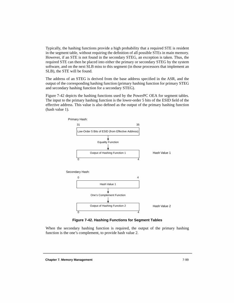
Chapter 7. Memory Management 7-99
Typically, the hashing functions provide a high probability that a required STE is residentin the segment table, without requiring the definition of all possible STEs in main memory.However, if an STE is not found in the secondary STEG, an exception is taken. Thus, therequired STE can then be placed into either the primary or secondary STEG by the systemsoftware, and on the next SLB miss to this segment (in those processors that implement anSLB), the STE will be found.
The address of an STEG is derived from the base address specified in the ASR, and theoutput of the corresponding hashing function (primary hashing function for primary STEGand secondary hashing function for a secondary STEG).
Figure 7-42 depicts the hashing functions used by the PowerPC OEA for segment tables.The input to the primary hashing function is the lower-order 5 bits of the ESID field of theeffective address. This value is also defined as the output of the primary hashing function(hash value 1).
Figure 7-42. Hashing Functions for Segment Tables
When the secondary hashing function is required, the output of the primary hashingfunction is the one’s complement, to provide hash value 2.
Equality Function
Low-Order 5 Bits of ESID (from Effective Address)
31 35
Primary Hash:
Output of Hashing Function 1
0 4
Secondary Hash:
Hash Value 1
0 4
Hash Value 1
Hash Value 2
One’s Complement Function
Output of Hashing Function 2
0 4

7-100 PowerPC Microprocessor Family: The Programming Environments, Rev. 1
7.7.1.3 Segment Table Address GenerationThe following sections illustrate the generation of the addresses used for accessing thehashed segment tables. As stated earlier, the operating system must synthesize the segmenttable search algorithm for setting up the tables.
The base address of the segment table is defined by the higher-order 52 bits of ASR. Bits52–56 of the STEG address are derived from the hash value. Depending on whether theprimary or secondary STEG is to be accessed, the processor uses either the primary orsecondary hashing function as described in Section 7.7.1.2, “Segment Table HashingFunctions.” Bits 57–63 of the STEG address are zero. In the process of searching for anSTE, the processor first checks STE0 (at the STEG base address). Figure 7-43 provides agraphical description of the generation of the STEG addresses. Note that Figure 7-43 is alsoan expansion of the virtual address generation shown in Figure 7-17.
In the process of searching for an STE, the processor interprets the values read frommemory as described in Section 7.5.2.1.1, “STE Format—64-Bit Implementations.” Theentire ESID field of the effective address of the access is compared to the same field of theSTEs in memory. In addition, the valid (V) bit is also checked. For a hit to occur, the V bitof the STE in memory must be set. If the ESID field matches and the entry is valid, the STEis considered a hit.
Note that in the case of the segment table, the H bit (defined for PTEs) is not required todistinguish between the primary and secondary STEs. Because the entire ESID field of theaccess is compared with the entire ESID field of the STE, when there is a hit, the STEshould contain the unique mapping of effective to virtual address for the access (providedthere are no programming errors).
During a segment table search operation, the processor compares up to 16 STEs:STE0–STE7 of the primary STEG (defined by the primary hashing function) andSTE0–STE7 of the secondary STEG (defined by the secondary hashing function). If theESID field does not match (or if V is not set) for any of these STEs, a segment faultexception condition occurs and an exception is taken. Thus, if no matching (and valid) STEis found for an access, the operating system must load the STE into the segment table.
TEMPORARY 64-BIT BRIDGE
Note that although processors using the 64-bit bridge implement STEs as defined for 64-bit implementations, the use of the segment table hashing function is not required becauseonly 16 segment descriptors are required to define the entire 32-bit (4 Gbyte) addressspace. These segment descriptors are defined as STEs and are stored in 16 SLB entriesdesignated for that purpose.

Chapter 7. Memory Management 7-101
The architecture does not specify the order in which the STEs are checked. Note that formaximum performance, STEs should be allocated by the operating system first beginningwith the STE0 location within the primary STEG, then STE1, and so on. If more than eightSTEs are required within the address space that defines a STEG address, the secondarySTEG can be used (again, allocation of STE0 of the secondary STEG first, and so on isrecommended). Additionally, it may be desirable to place the STEs that will require mostfrequent access at the beginning of a STEG and reserve the STEs in the secondary STEGfor the least frequently accessed STEs.
The architecture also allows for multiple matching STEs to be found within a table searchoperation. However, multiple matching STEs must be identical in all fields. Otherwise, thetranslation is undefined.

7-102 PowerPC Microprocessor Family: The Programming Environments, Rev. 1
Figure 7-43. Generation of Addresses for Segment Table
SEGMENT TABLE(4 Kbytes)
STE0
128 Bytes
64-Bit Effective Address
STE716 Bytes
80-Bit Virtual Address
ESID(36 Bit)
V T
Virtual Segment ID (VSID)(52 Bit)
0 51 52 63
Hash Function
STEG0
STEG31
STE0 35 36 55 56 57 58 59 60 61 63
00. . . . .00
ESID Page Index Byte Offset(36 Bit) (16 Bit) (12 Bit)
0 30 31 35 36 51 52 63
Address Space Register (ASR)Physical Address of Segment Table
(52 Bit)
0 51 52 63
64-Bit Physical Address ofSegment Table Entry Group
0 51 52 56 57 63
STEGSelect
0. . .0
00. . . .00
Segment Table Entry (STE)16 Bytes
KsKp
00000. . . 00
VSID Page Index Byte Offset(52 Bit) (16 Bit) (12 Bit)
Virtual Page Number
N

Chapter 7. Memory Management 7-103
7.7.1.4 Segment Table in 32-Bit ModeAs stated earlier, the only effect on the MMU of operating in 32-bit mode (MSR[SF] = 0)is that the upper-order 32 bits of the logical (effective) address are truncated (treated aszero). Thus, only the lower-order four bits of the ESID field of the effective address are usedin the address translation. These four bits select one of 16 STEGs in the segment table andcorrespond to the highest-order four bits of an address that would have been generated bya 32-bit implementation. The 16 STEGs can then be used in a way similar to the 16 segmentregisters defined for 32-bit implementations.
7.7.1.5 Segment Table Structure (with Examples)This section contains an example of an effective address and how its segment descriptor(the STE) maps into the primary STEG in physical memory. The example illustrates howthe processor generates STEG addresses for a segment table search operation; this is alsothe algorithm that must be used by the operating system in creating the segment tables.
In the example shown in Figure 7-44, the value in ASR defines a segment table at address0x0000_5C80_42A1_7000 that contains 32 STEGs (all segment tables are defined with asize of 4 Kbytes). The highest-order 36 bits of the effective address are then used to locatethe corresponding STE in the segment table. The contents of the STE are then used alongwith bits 36–63 of the effective address and the 12-bit byte offset to create the 80-bit virtualaddress.
TEMPORARY 64-BIT BRIDGE
Note that operating systems using features of the 64-bit bridge run in 32-bit mode, and justas is the case for 32-bit mode described in the previous paragraph, only 16 segmentdescriptors are required. When ASR[V] bit is cleared, the ASR[STABORG], whichindicates the starting address of the segment table is considered to be invalid. The 16segment registers are implemented in 16 SLB entries as required by the 64-bit bridgearchitecture.
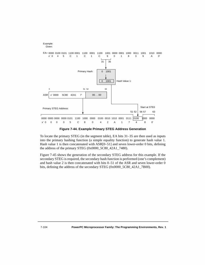
7-104 PowerPC Microprocessor Family: The Programming Environments, Rev. 1
Figure 7-44. Example Primary STEG Address Generation
To locate the primary STEG (in the segment table), EA bits 31–35 are then used as inputsinto the primary hashing function (a simple equality function) to generate hash value 1.Hash value 1 is then concatenated with ASR[0–51] and seven lower-order 0 bits, definingthe address of the primary STEG (0x0000_5C80_42A1_7480).
Figure 7-45 shows the generation of the secondary STEG address for this example. If thesecondary STEG is required, the secondary hash function is performed (one’s complement)and hash value 2 is then concatenated with bits 0–51 of the ASR and seven lower-order 0bits, defining the address of the secondary STEG (0x0000_5C80_42A1_7B00).
Primary STEG Address:
0000 0000 0000 0000 0101 1100 1000 0000 0100 0010 1010 0001 0111 0100 1000 0000
x’ 0 0 0 0 5 C 8 0 4 2 A 1 7 4 8 0’
EA=
Start at STE0
6356 57
Example:Given:
31 35
Primary Hash: 0 1001
0 1001 Hash Value 1:
ASR
0 51 52 63
00. . . 00x’ 0000 5C80 42A1 7’
51 52
0000 0100 0101 1100 0001 1100 0001 1100 1001 0000 0001 1000 0011 1001 1010 0000x’ 0 4 5 C 1 C 1 C 9 0 1 8 3 9 A 0’

Chapter 7. Memory Management 7-105
Figure 7-45. Example Secondary STEG Address Generation
As described earlier, because the entire effective segment ID field of the STE is comparedwith the effective segment ID field of the effective address, when an STE compare processresults in a match (hit) with the effective address, the STE mapping should be the uniqueSTE required (provided there are no programming errors).
Note, however, that a given STEG address does not map back to a unique effective address.Not only can a given STEG be considered both a primary and a secondary STEG, but manyof the bits of the effective segment ID in the effective address are not used to generate theSTEG address. Therefore, any combination of these unused bits will map to the same pairof STEG addresses.
(from
Secondary STEG Address:
0000 0000 0000 0000 0101 1100 1000 0000 0100 0010 1010 0001 0111 1011 0000 0000
x’ 0 0 0 0 5 C 8 0 4 2 A 1 7 B 0 0’
Start at STE0
6356 57
Secondary Hash: 0 1001
1 0110Hash Value 2:
51 52
0 1001
One’s Complement
Hash Value 1:

7-106 PowerPC Microprocessor Family: The Programming Environments, Rev. 1
7.7.2 Segment Table Search Operation The segment table search process performed by a PowerPC processor in the search of anSTE is analogous to the page table search algorithm described earlier for PTEs and is asfollows:
1. The 64-bit physical addresses of the primary and secondary STEGs are generated as described in Section 7.7.1.3, “Segment Table Address Generation.”
2. As many as 16 STEs (from the primary and secondary STEGs) are read from memory (the architecture does not specify the order of these reads, allowing multiple reads to occur in parallel). STE reads occur with an implied WIM memory/cache mode control bit setting of 0b001. Therefore, they are considered cacheable.
3. The STEs in the selected STEGs are tested for a match with the effective segment ID (ESID) of the access. For a match to occur, the following must be true:
— STE[V] = 1— STE[ESID] = EA[0–35]
4. If no match is found within the eight STEs of the primary STEG and the eight STEs of the secondary STEG, an exception is generated as described in step 7. If a match (or multiple matches) is found, the table search process continues.
5. If multiple matches are found, they must be identical in all defined fields. Otherwise, the translation is undefined.
6. If a match is found, the STE is written into the on-chip SLB (if implemented) and the segment table search is complete.
7. If a match is not found within the primary or secondary PTEG, the search fails, and an exception condition (a page fault) occurs (either an ISI or a DSI exception).
Reads from memory for segment table search operations are performed as if the WIMG bitsettings were 0b0010 (that is, as unguarded cacheable operations in which coherency isrequired).
Figure 7-46 provides a detailed flow diagram of a segment table search operation. Note thatthe references to SLBs are shown as optional because SLBs are not required; if they doexist, the specifics of how they are maintained are implementation-specific.

Chapter 7. Memory Management 7-107
Figure 7-46. Segment Table Search Flow
7.7.3 Segment Table Updates This section describes the requirements on the software when updating segment tables inmemory via some pseudocode examples; note that these requirements are very similar tothe requirements imposed on the updating of page tables, but do not have the complicationof hardware updates to the referenced and changed bits.
Multiprocessor systems must follow the rules described in this section so that all processorsoperate with a consistent set of segment tables. Even single processor systems must followcertain rules, because software changes must be synchronized with the other instructions inexecution. Updates to the tables include the following operations:
• Adding an STE• Modifying an STE • Deleting an STE
Generate Primary and SecondarySTEG Addresses
Fetch STE(s) from Physical Address(es)
otherwise
otherwise
Adjust PA to Read More STEs
Write STE into SLB
Segment Table Search
STE [ESID, V]= EA [ESID], 1
Segment Table Search Complete
DSI ExceptionISI Exception
SRR1[42] ← 1 DSISR[10] ← 1
Data AccessInstruction Access
all 16 STEs checked
Implementation-specificNote:
segment fault

7-108 PowerPC Microprocessor Family: The Programming Environments, Rev. 1
STEs must be locked on multiprocessor systems. Access to STEs must be appropriatelysynchronized by software locking of (that is, guaranteeing exclusive access to) STEs orSTEGs if more than one processor can modify the table at that time. In the examples in thefollowing section, lock() and unlock() refer to software locks that must be performed toprovide exclusive access to the STE being updated. However, the architecture does notdictate the specific protocol to be used for locking. See Appendix E, “SynchronizationProgramming Examples,” for more information about the use of the reservation instructions(such as the lwarx and stwcx. instructions) to perform software locking.
On single processor systems, STEs need not be locked. To adapt the examples given belowfor the single processor case, simply delete the ‘lock()’ and ‘unlock()’ lines from theexamples. The sync instructions shown are required even for single processor systems (toensure that all previous changes to the segment tables have completed).
When SLBs are implemented, they are defined as noncoherent caches of the segmenttables. SLB entries must be invalidated explicitly with the SLB invalidate entry instruction(slbie) whenever the corresponding STE is modified. The sync instruction causes theprocessor to wait until the SLB invalidate operation in progress by this processor iscomplete.
Any processor, including the processor modifying the segment table, may access thesegment table at any time in an attempt to reload a SLB entry. An inconsistent segment tableentry must never accidentally become visible (if V = 1); thus, there must be synchronizationbetween modifications to the valid bit and any other modifications.
As is the case with PTEs, STEs must not be changed in a manner that causes an implicitbranch. Section 2.3.18, “Synchronization Requirements for Special Registers and forLookaside Buffers,” lists the possible implicit branch conditions that can occur whensystem registers and MSR bits are changed and a complete list of the synchronizationrequirements for executing the MMU instructions.
The following examples show the required sequence of operations. However, otherinstructions may be interleaved within the sequences shown.
7.7.3.1 Adding a Segment Table EntryAdding a segment table entry requires only a lock on the STE in a multiprocessor system.The first bytes in the STE are then written (this example assumes the old valid bit wascleared), the eieio instruction orders the update and then the second update can be made. Async instruction ensures that the updates have been made to memory.
TEMPORARY 64-BIT BRIDGE
Note that in the 64-bit bridge, 16 SLB entries are used to hold the 16 segment descriptorsnecessary for defining the 32-bit address space.
Chapter 7. Memory Management 7-109
lock(STE)if T = 0,
then
STE[VSID] ← new valueeieio /* order 1st STE update before 2ndSTE[ESID, V, T, Ks, Kp, N] ← new values (Note: N bit only for T = 0 segments)
else (note that the T = 1 functionality is being phased out of the architecture)STE[0b1,CNTLR_SPEC] ← new valueseieio /* order 1st STE update before 2ndSTE[ESID, V, T, Ks, Kp, 0b0] ← new values (V = 1)
sync /* ensure updates completedunlock(STE)
7.7.3.2 Modifying a Segment Table EntryTo change the contents of a currently-valid STE, the STE must be locked, invalidated,updated, invalidated from the SLB, marked valid again, and unlocked. The sync instructionmust be used at appropriate times to wait for modifications to complete.
lock(STE)STE[V] ← 0 /* other fields don’t mattersync /* ensure update completedif T = 0,
then
STE[VSID] ← new valueeieio /* order 2nd STE update before 3rdSTE[ESID,V, T, Ks, Kp, N] ← new values (Note: N bit only for T = 0 segments)
else (note that the T = 1 functionality is being phased out of the architecture)STE[0b1,CNTLR_SPEC] ← new valueeieio /* order 2nd STE update before 3rdSTE[ESID, V, T, Ks, Kp, 0b0] ← new value (V = 1)
slbie(old_EA) /* invalidate old translationsync /* ensure slbie and last update completedunlock(STE)
7.7.3.3 Deleting a Segment Table EntryIn this example, the entry is locked, marked invalid, invalidated in the SLB, and unlocked.
lock(STE)STE[V] ← 0 /* (other fields don’t matter)sync /* ensure update completedslbie(old_EA) /* invalidate old translationsync /* ensure slbie completedunlock(STE)
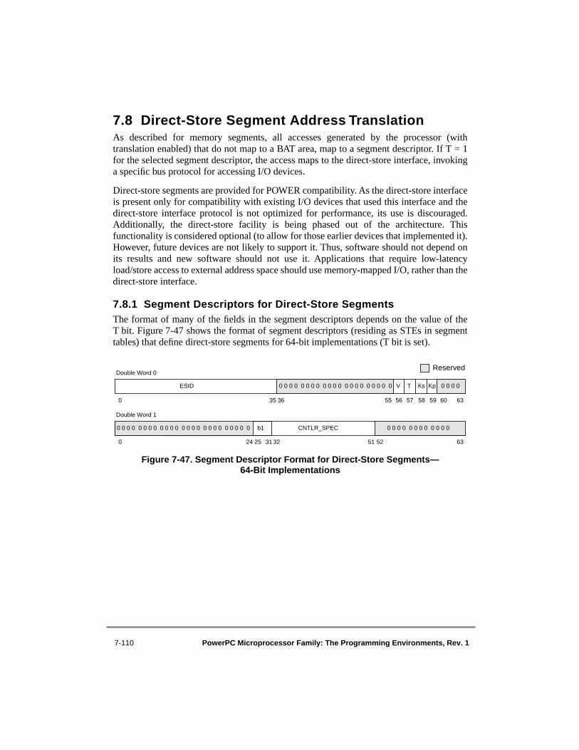
7-110 PowerPC Microprocessor Family: The Programming Environments, Rev. 1
7.8 Direct-Store Segment Address TranslationAs described for memory segments, all accesses generated by the processor (withtranslation enabled) that do not map to a BAT area, map to a segment descriptor. If T = 1for the selected segment descriptor, the access maps to the direct-store interface, invokinga specific bus protocol for accessing I/O devices.
Direct-store segments are provided for POWER compatibility. As the direct-store interfaceis present only for compatibility with existing I/O devices that used this interface and thedirect-store interface protocol is not optimized for performance, its use is discouraged.Additionally, the direct-store facility is being phased out of the architecture. Thisfunctionality is considered optional (to allow for those earlier devices that implemented it).However, future devices are not likely to support it. Thus, software should not depend onits results and new software should not use it. Applications that require low-latencyload/store access to external address space should use memory-mapped I/O, rather than thedirect-store interface.
7.8.1 Segment Descriptors for Direct-Store SegmentsThe format of many of the fields in the segment descriptors depends on the value of theT bit. Figure 7-47 shows the format of segment descriptors (residing as STEs in segmenttables) that define direct-store segments for 64-bit implementations (T bit is set).
Figure 7-47. Segment Descriptor Format for Direct-Store Segments—64-Bit Implementations
0 24 25 31 32 51 52 63
Reserved
0 35 36 55 56 57 58 59 60 63
ESID 0 0 0 0 0 0 0 0 0 0 0 0 0 0 0 0 0 0 0 0 0 V T Ks Kp 0 0 0 0
Double Word 0
Double Word 1
0 0 0 0 0 0 0 0 0 0 0 0 0 0 0 0 0 0 0 0 0 0 0 0 0 b1 CNTLR_SPEC 0 0 0 0 0 0 0 0 0 0 0 0

Chapter 7. Memory Management 7-111
Table 7-28 shows the bit definitions for the segment descriptors when the T bit is set for 64-bit implementations.
In 32-bit implementations, the segment descriptors reside in one of 16 on-chip segmentregisters. Figure 7-48 shows the register format for the segment registers when the T bit isset for 32-bit implementations.
Figure 7-48. Segment Register Format for Direct-Store Segments—32-Bit Implementations
Table 7-29 shows the bit definitions for the segment registers when the T bit is set for 32-bitimplementations.
Table 7-28. Segment Descriptor Bit Definitions for Direct-Store Segments—64-Bit Implementations
Double Word Bit Name Description
0 0–35 ESID Effective segment ID
36–55 — Reserved
56 V Entry valid (V = 1) or invalid (V = 0)
57 T T = 1 selects this format
58 Ks Supervisor-state protection key
59 Kp User-state protection key
60–63 — Reserved
1 0–24 — Reserved
25–31 b1 Bits 2–8 of the BUID
32–51 CNTLR_SPEC Controller-specific information
52–63 — Reserved
Table 7-29. Segment Register Bit Definitions for Direct-Store Segments
Bit Name Description
0 T T = 1 selects this format.
1 Ks Supervisor-state protection key
2 Kp User-state protection key
3–11 BUID Bus unit ID
12–31 CNTLR_SPEC Device-specific data for I/O controller
T Ks Kp BUID CNTLR_SPEC
0 1 2 3 11 12 31
7-112 PowerPC Microprocessor Family: The Programming Environments, Rev. 1
7.8.2 Direct-Store Segment AccessesWhen the address translation process determines that the segment descriptor has T = 1,direct-store segment address translation is selected; no reference is made to the page tablesand neither the referenced or changed bits are updated. These accesses are performed as ifthe WIMG bits were 0b0101; that is, caching is inhibited, the accesses bypass the cache,hardware-enforced coherency is not required, and the accesses are considered guarded.
The specific protocol invoked to perform these accesses involves the transfer of address anddata information; however, the PowerPC OEA does not define the exact hardware protocolused for direct-store accesses. Some instructions may cause multiple address/datatransactions to occur on the bus. In this case, the address for each transaction is handledindividually with respect to the MMU.
The following describes the data that is typically sent to the memory controller byprocessors that implement the direct-store function:
• One of the Kx bits (Ks or Kp) is selected to be the key as follows:
— For supervisor accesses (MSR[PR] = 0), the Ks bit is used and Kp is ignored.
— For user accesses (MSR[PR] = 1), the Kp bit is used and Ks is ignored.
• An implementation-dependent portion of the segment descriptor.
• An implementation-dependent portion of the effective address.
7.8.3 Direct-Store Segment ProtectionPage-level memory protection as described in Section 7.5.4, “Page Memory Protection,” isnot provided for direct-store segments. The appropriate key bit (Ks or Kp) from the segmentdescriptor is sent to the memory controller, and the memory controller implements anyprotection required. Frequently, no such mechanism is provided; the fact that a direct-storesegment is mapped into the address space of a process may be regarded as sufficientauthority to access the segment.
7.8.4 Instructions Not Supported in Direct-Store SegmentsThe following instructions are not supported at all and cause either a DSI exception orboundedly-undefined results when issued with an effective address that selects a segmentdescriptor that has T = 1:
• lwarx and ldarx• stwcx. and stdcx.• eciwx• ecowx

Chapter 7. Memory Management 7-113
7.8.5 Instructions with No Effect in Direct-Store SegmentsThe following instructions are executed as no-ops when issued with an effective addressthat selects a segment where T = 1:
• dcba• dcbt• dcbtst• dcbf• dcbi• dcbst• dcbz
• icbi
7.8.6 Direct-Store Segment Translation Summary FlowFigure 7-49 shows the flow used by the MMU when direct-store segment addresstranslation is selected. This figure expands the Direct-Store Segment Translation stub foundin Figure 7-5 for both instruction and data accesses. In the case of a floating-point load orstore operation to a direct-store segment, it is implementation-specific whether thealignment exception occurs. In the case of an eciwx, ecowx, lwarx, ldarx, stwcx., or stdcx.instruction, the implementation either sets the DSISR as shown and causes the DSIexception, or causes boundedly-undefined results.

7-114 PowerPC Microprocessor Family: The Programming Environments, Rev. 1
Figure 7-49. Direct-Store Segment Translation Flow
Perform Direct-Store Interface Access
Data AccessInstruction Access
Direct-Store Segment Translation
T = 1
otherwise
Floating-PointLoad or Store
Alignment Exception
otherwise
Cache Instruction (dcbt, dcbtst, dcbf, dcbi, dcbst,
dcbz, or icbi)
No-Op
otherwise
DSI Exception or Boundedly Undefined Results
ISI Exception
DSISR[5] ← 1
eciwx, ecowx, lwarx, ldarx, stwcx., or stdcx. Instruction
SRR1[35*] ← 1
Notes:*Subtract 32 from bit number for bit setting in 32-bit implementations
Implementation-specific

Chapter 7. Memory Management 7-115
TEMPORARY 64-BIT BRIDGE
7.9 Migration of Operating Systems from 32-Bit Implementations to 64-Bit Implementations
The facilities and instructions described in this section may optionally be provided by a 64-bit implementation to reduce the amount of software change required to migrate anoperating system from a 32-bit implementation to a 64-bit implementation. Using thebridge facility allows the operating system to treat the MSR as a 32-bit register and tocontinue to use the segment register manipulation instructions (mtsr, mtsrin, mfsr, andmfsrin) which are defined for 32-bit implementations. These instructions are otherwiseillegal in the 64-bit architecture. Although the 64-bit bridge does not literally implement the16 registers as they are defined by the 32-bit portion of the architecture, the segment registermanipulation instructions are used to access the 16 predefined segment descriptors storedin the on-chip SLBs.
The bridge features do not conceal the differences in format of the page table, BATregisters, and SDR1 between 32-bit and 64-bit implementations—the operating systemmust be converted explicitly to use the 64-bit formats. Note that an operating system thatuses the bridge features does not take full advantage of the 64-bit implementation (forexample, it can generate only 32-bit effective addresses).
An operating system that uses the 64-bit bridge architecture should observe the following:
• The boot process should do the following:
— Clear MSR[SF] and MSR[ISF].
— Initialize the ASR, clearing ASR[V].
— Invalidate all SLB entries.
• The operating system should do the following:
— Support only 32-bit applications.
— If any 64-bit instructions are used, for example, to modify a PTE or a 64-bit SPR, ensure either that exceptions cannot occur or that the exception handler saves and restores all 64 bits of the GPRs.
— Manipulate only the low-order 32 bits of the MSR, leaving the high-order 32 bits unchanged.
— Always have MSR[ISF] = 0 and ASR[V] = 0.
— Manage virtual segments using the 32-bit segment register manipulation instructions (mtsr, mtsrin, mfsr, and mfsrin).
— Always map segments 0–15 in the SLB when translation is enabled. They may be mapped with a VSID for which there are no valid PTEs.
— Never execute an slbie or slbia instruction.
— Never generate an effective address greater than 232 – 1 when MSR[SF] = 1.

7-116 PowerPC Microprocessor Family: The Programming Environments, Rev. 1
7.9.1 ISF Bit of the Machine State RegisterMSR[ISF] (bit 2) may optionally be used by a 64-bit implementation to control the mode(64-bit or 32-bit) that is entered when an exception is taken. If MSR[ISF] is implemented,it has the properties described below. If it is not implemented, it is treated as reserved exceptthat ISF is assumed to be set for exception handling.
• When an exception occurs, MSR[ISF] is copied to MSR[SF].
• When an exception occurs, MSR[ISF] is not altered.
• No software synchronization is required before or after altering MSR[ISF] (see Section 2.3.18, “Synchronization Requirements for Special Registers and for Lookaside Buffers”).
7.9.2 rfi and mtmsr Instructions in a 64-Bit ImplementationThe rfi and mtmsr instruction pair may be implemented in some 64-bit implementations,along with the rfid and mtmsrd instructions, which are required by 64-bitimplementations. A 64-bit processor must implement either both or neither of theseinstructions. Attempting to execute either rfi or mtmsr on a 64-bit processor that does notsupport these instructions causes an illegal instruction type program exception.
Except for the following variances, the operation of these instructions in a 64-bitimplementation is identical to their operation in a 32-bit implementation as described inSection 4.4.1, “System Linkage Instructions—OEA,” and Section 4.4.3.2, “SegmentRegister Manipulation Instructions.”
• rfi
— The SRR1 bits that are copied to the corresponding bits of the MSR are bits 48–55, 57–59 and 62–63 of SRR1. Note that depending on the implementation, additional bits from SRR1 may be restored to the MSR. The remaining bits of the MSR, including the high-order 32 bits, are unchanged.
— If the new MSR value does not enable any pending exceptions, the next instruction is fetched, under control of the new MSR value, from the address SRR0[0–61]||0b00 (when SF is set in the new MSR value) or (32)0||SRR0[32–61]||0b00 (when SF is cleared in the new MSR value).
• mtmsr
— Bits 32–63 of rS are placed into MSR[32–63]. MSR[0–31] are unchanged.
Note that an additional 64-bit–specific instruction for reading the MSR is not needed because the mfmsr instruction copies the entire contents of the MSR to the selected GPR in both 32- and 64-bit implementations.

Chapter 7. Memory Management 7-117
7.9.3 Segment Register Manipulation Instructions in the 64-Bit Bridge
The four segment register manipulation instructions, mtsr, mtsrin, mfsr, and mfsrin,defined as part of the 32-bit portion of the architecture may optionally be provided by a 64-bit implementation that uses the 64-bit bridge. As part of the 64-bit bridge, theseinstructions operate as described below rather than in the way they are described for 32-bitimplementations (as described in Section 4.4.3.2, “Segment Register ManipulationInstructions.”) These instructions are implemented as a group and are not implementedindividually. Attempting to execute one of these instructions on a 64-bit processor on whichit is not supported causes an illegal instruction type program exception.
These instructions allow software to associate effective segments 0 through 15 with any ofvirtual segments 0 through 224 – 1 without altering the segment table in memory. Sixteenindexed SLB entries serve as virtual segment registers. The mtsr and mtsrin instructionsmove 32 bits from a selected GPR to a selected SLB entry. The mfsr and mfsrininstructions move 64 bits from a selected SLB entry to a selected GPR and can be used toread an SLB entry that was created with mtsr, mtsrin, mtsrd, or mtsrdin.
The software synchronization requirements for any of the move to segment registerinstructions in a 64-bit implementation are the same as for those defined by the 32-bitarchitecture.
To ensure that SLB entries contain unique ESIDs when the bridge is used, an ESID mappedby any of the move to segment register instructions must not have been mapped to that SLBentry by the segment table when ASR[V] was set.
If an SLB entry that software established using one of the move to segment registerinstructions is overwritten while ASR[V] = 1, software must be able to handle anyexception caused when a segment descriptor cannot be located.
Executing an mfsr or mfsrin instruction may set rD to an undefined value if ASR[V] hasbeen set at any time since execution of the mtsr, mtsrin, mtsrd, or mtsrdin instruction thatestablished the selected SLB entry, because that SLB entry may have been overwritten bythe processor in the meantime.
Typically, 16 fixed SLB entries are used by the segment register manipulation instructions,while SLB reload from the segment table selects SLB entries based on some otherreplacement policy such as LRU.
With respect to updating any SLB replacement history used by the SLB replacement policy,implementations will treat the execution of an mtsr, mtsrd, mtsrin, or mtsrdin instructionthe same as an SLB reload from the segment table.
The following sections describe the move to and move from segment register instructionsas they are defined for the 64-bit bridge.

7-118 PowerPC Microprocessor Family: The Programming Environments, Rev. 1
7.9.4 64-Bit Bridge Implementation of Segment Register Instructions Previously Defined for 32-Bit Implementations Only
The following sections describe the mfsr, mfsrin, mtsr, and mtsrin instructions that aredefined for the 32-bit architecture and are allowed in the 64-bit bridge architecture only ifASR[V] is implemented. Otherwise, attempting to execute one of these instructions isillegal on a 64-bit implementation.
7.9.4.1 Move from Segment Register—mfsr As in the 32-bit architecture, the mfsr instruction syntax is as follows:
mfsr rD,SR
The operation of the instruction is described as follows:
rD ← SLB(SR)
When executed as part of the 64-bit bridge, the contents of the SLB entry selected by SRare placed into rD; the contents of rD correspond to a segment table entry containing valuesas shown in Table 7-30.
If the SLB entry selected by SR was not created by an mtsr, mtsrd, or mtsrdin instruction,the contents of rD are undefined. Formatting for GPR contents is shown in Figure 7-50.Fields shown as x’s are ignored. Fields shown as slashes correspond to reserved bits in thesegment table entry. Note that the T = 1 (direct-store) facility is being phased out of thearchitecture and future processors are not likely to support it.
This is a supervisor-level instruction.
Table 7-30. Contents of rD after Executing mfsr
Double Word Bit(s) Contents Description
0 0–31 0x0000_0000 ESID[0–31]
32–35 SR ESID[32–35]
36–56 — —
57–59 rD[32–34] T, Ks, Kp
60–61 rD[35–36] N, reserved bit, or b0
62–63 — —
1 0–24 rD[7–31] VSID[0–24] (or reserved if SR[T] = 1)
25–51 rD[37–63] VSID[25–51] (or b1 and CNTLR_SPEC if SR[T] = 1)
52–63 — —
Note: The contents of rD[0–6] are cleared automatically.
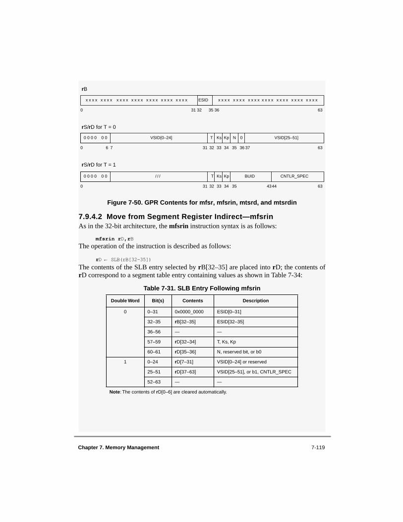
Chapter 7. Memory Management 7-119
Figure 7-50. GPR Contents for mfsr, mfsrin, mtsrd, and mtsrdin
7.9.4.2 Move from Segment Register Indirect—mfsrin As in the 32-bit architecture, the mfsrin instruction syntax is as follows:
mfsrin rD,rB
The operation of the instruction is described as follows:
rD ← SLB(rB[32–35])
The contents of the SLB entry selected by rB[32–35] are placed into rD; the contents ofrD correspond to a segment table entry containing values as shown in Table 7-34:
Table 7-31. SLB Entry Following mfsrin
Double Word Bit(s) Contents Description
0 0–31 0x0000_0000 ESID[0–31]
32–35 rB[32–35] ESID[32–35]
36–56 — —
57–59 rD[32–34] T, Ks, Kp
60–61 rD[35–36] N, reserved bit, or b0
1 0–24 rD[7–31] VSID[0–24] or reserved
25–51 rD[37–63] VSID[25–51], or b1, CNTLR_SPEC
52–63 — —
Note: The contents of rD[0–6] are cleared automatically.
0 6 7 31 32 33 34 35 36 37 63
0 0 0 0 0 0 VSID{0–24] T Ks Kp N 0 VSID[25–51]
0 31 32 35 36 63
x x x x x x x x x x x x x x x x x x x x x x x x x x x x ESID x x x x x x x x x x x x x x x x x x x x x x x x x x x x
0 31 32 33 34 35 4344 63
0 0 0 0 0 0 / / / T Ks Kp BUID CNTLR_SPEC
rS/rD for T = 0
rB
rS/rD for T = 1

7-120 PowerPC Microprocessor Family: The Programming Environments, Rev. 1
If the SLB entry selected by rB[32–35] was not created by an mtsr, mtsrd, or mtsrdininstruction, the contents of rD are undefined. Formatting for GPR contents is shown inFigure 7-50. Fields shown as x’s are ignored. Fields shown as slashes correspond toreserved bits in the segment table entry. Note that the T = 1 (direct-store) facility is beingphased out of the architecture and future processors are not likely to support it.
This is a supervisor-level instruction.
7.9.4.3 Move to Segment Register—mtsrAs in the 32-bit architecture, the mtsr instruction syntax is as follows:
mtsr SR,rS
The operation of the instruction is described as follows:
SLB(SR) ← (rS[32–63])
The SLB entry selected by SR is set as though it were loaded from a segment table entry,as shown in Table 7-32.
This is a supervisor-level instruction. Formatting for GPR contents is shown in Figure 7-51.Fields shown as x’s are ignored. Fields shown as slashes correspond to reserved bits in thesegment table entry. Note that the T = 1 (direct-store) facility is being phased out of thearchitecture and future processors are not likely to support it.
Table 7-32. SLB Entry Following mtsr
Double Word Bit(s) Contents Description
0 0–31 0x0000_0000 ESID[0–31]
32–35 SR ESID[32–35]
36–55 — —
56 0b1 V
57–59 rS[32–34] T, Ks, Kp
60–61 rS[35–36] N, reserved bit, or b0
62–63 — —
1 0–24 0x0000_00||0b0 VSID[0–24] or reserved
25–51 rS[37–63] VSID[25–51], or b1, CNTLR_SPEC
51–63 — —

Chapter 7. Memory Management 7-121
Figure 7-51. GPR Contents for mtsr and mtsrin
Note that when creating a memory segment (T = 0) using the mtsr instruction, rS[36–39]should be cleared, as these bits correspond to the reserved bits in the T = 0 format for asegment register.
7.9.4.4 Move to Segment Register Indirect—mtsrinAs in the 32-bit architecture, the mtsrin instruction syntax is as follows:
mtsrin rS,rB
The operation of the instruction is described as follows:
SLB(rB[32–35]) ← (rS[32–63])
The SLB entry selected by bits 32–35 of rB is set as though it were loaded from a segmenttable entry, as shown in Table 7-34.
Table 7-33. SLB Entry Following mtsrin
Double Word Bit(s) Contents Description
0 0–31 0x0000_0000 ESID[0–31]
32–35 rB[32–35] ESID[32–35]
36–55 — —
56 0b1 V
57–59 rS[32–34] T, Ks, Kp
60–61 rS[35–36] N, reserved bit, or b0
62–63 — —
0 3132 33 34 35 36 39 40 63
x x x x x x x x x x x x x x x x x x x x x x x x x x x x T Ks Kp N 0 0 0 0 VSID[28–51]
rS for T = 0
rB
0 31 32 35 36 63
x x x x x x x x x x x x x x x x x x x x x x x x x x x x ESID x x x x x x x x x x x x x x x x x x x x x x x x x x x x
0 3132 33 34 35 43 44 63
x x x x x x x x x x x x x x x x x x x x x x x x x x x x T Ks Kp BUID VSID[28–51]
rS for T = 1
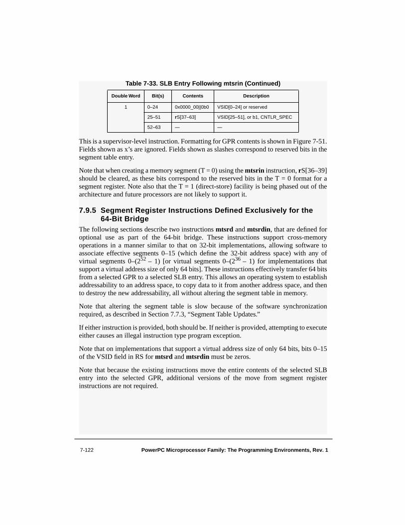
7-122 PowerPC Microprocessor Family: The Programming Environments, Rev. 1
This is a supervisor-level instruction. Formatting for GPR contents is shown in Figure 7-51.Fields shown as x’s are ignored. Fields shown as slashes correspond to reserved bits in thesegment table entry.
Note that when creating a memory segment (T = 0) using the mtsrin instruction, rS[36–39]should be cleared, as these bits correspond to the reserved bits in the T = 0 format for asegment register. Note also that the T = 1 (direct-store) facility is being phased out of thearchitecture and future processors are not likely to support it.
7.9.5 Segment Register Instructions Defined Exclusively for the 64-Bit Bridge
The following sections describe two instructions mtsrd and mtsrdin, that are defined foroptional use as part of the 64-bit bridge. These instructions support cross-memoryoperations in a manner similar to that on 32-bit implementations, allowing software toassociate effective segments 0–15 (which define the 32-bit address space) with any ofvirtual segments 0–(252 – 1) [or virtual segments 0–(236 – 1) for implementations thatsupport a virtual address size of only 64 bits]. These instructions effectively transfer 64 bitsfrom a selected GPR to a selected SLB entry. This allows an operating system to establishaddressability to an address space, to copy data to it from another address space, and thento destroy the new addressability, all without altering the segment table in memory.
Note that altering the segment table is slow because of the software synchronizationrequired, as described in Section 7.7.3, “Segment Table Updates.”
If either instruction is provided, both should be. If neither is provided, attempting to executeeither causes an illegal instruction type program exception.
Note that on implementations that support a virtual address size of only 64 bits, bits 0–15of the VSID field in RS for mtsrd and mtsrdin must be zeros.
Note that because the existing instructions move the entire contents of the selected SLBentry into the selected GPR, additional versions of the move from segment registerinstructions are not required.
1 0–24 0x0000_00||0b0 VSID[0–24] or reserved
25–51 rS[37–63] VSID[25–51], or b1, CNTLR_SPEC
52–63 — —
Table 7-33. SLB Entry Following mtsrin (Continued)
Double Word Bit(s) Contents Description
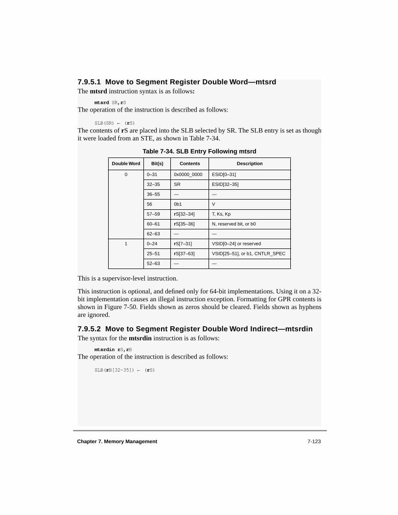
Chapter 7. Memory Management 7-123
7.9.5.1 Move to Segment Register Double Word—mtsrdThe mtsrd instruction syntax is as follows:
mtsrd SR,rS
The operation of the instruction is described as follows:
SLB(SR) ← (rS)
The contents of rS are placed into the SLB selected by SR. The SLB entry is set as thoughit were loaded from an STE, as shown in Table 7-34.
This is a supervisor-level instruction.
This instruction is optional, and defined only for 64-bit implementations. Using it on a 32-bit implementation causes an illegal instruction exception. Formatting for GPR contents isshown in Figure 7-50. Fields shown as zeros should be cleared. Fields shown as hyphensare ignored.
7.9.5.2 Move to Segment Register Double Word Indirect—mtsrdin The syntax for the mtsrdin instruction is as follows:
mtsrdin rS,rB
The operation of the instruction is described as follows:
SLB(rB[32-35]) ← (rS)
Table 7-34. SLB Entry Following mtsrd
Double Word Bit(s) Contents Description
0 0–31 0x0000_0000 ESID[0–31]
32–35 SR ESID[32–35]
36–55 — —
56 0b1 V
57–59 rS[32–34] T, Ks, Kp
60–61 rS[35–36] N, reserved bit, or b0
62–63 — —
1 0–24 rS[7–31] VSID[0–24] or reserved
25–51 rS[37–63] VSID[25–51], or b1, CNTLR_SPEC
52–63 — —
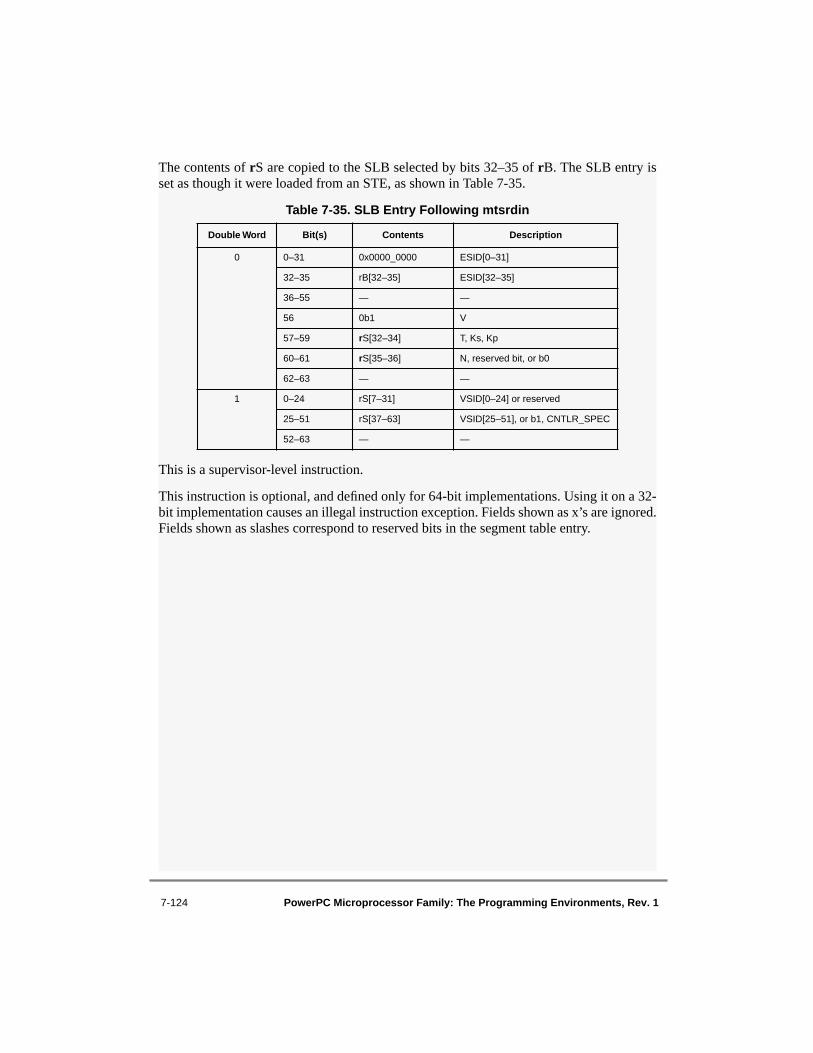
7-124 PowerPC Microprocessor Family: The Programming Environments, Rev. 1
The contents of rS are copied to the SLB selected by bits 32–35 of rB. The SLB entry isset as though it were loaded from an STE, as shown in Table 7-35.
This is a supervisor-level instruction.
This instruction is optional, and defined only for 64-bit implementations. Using it on a 32-bit implementation causes an illegal instruction exception. Fields shown as x’s are ignored.Fields shown as slashes correspond to reserved bits in the segment table entry.
Table 7-35. SLB Entry Following mtsrdin
Double Word Bit(s) Contents Description
0 0–31 0x0000_0000 ESID[0–31]
32–35 rB[32–35] ESID[32–35]
36–55 — —
56 0b1 V
57–59 rS[32–34] T, Ks, Kp
60–61 rS[35–36] N, reserved bit, or b0
62–63 — —
1 0–24 rS[7–31] VSID[0–24] or reserved
25–51 rS[37–63] VSID[25–51], or b1, CNTLR_SPEC
52–63 — —

Chapter 8. Instruction Set 8-1
Chapter 8 Instruction Set8080
This chapter lists the PowerPC instruction set in alphabetical order by mnemonic. Note thateach entry includes the instruction formats and a quick reference ‘legend’ that providessuch information as the level(s) of the PowerPC architecture in which the instruction maybe found—user instruction set architecture (UISA), virtual environment architecture(VEA), and operating environment architecture (OEA); and the privilege level of theinstruction—user- or supervisor-level (an instruction is assumed to be user-level unless thelegend specifies that it is supervisor-level); and the instruction formats. The formatdiagrams show, horizontally, all valid combinations of instruction fields; for a graphicalrepresentation of these instruction formats, see Appendix A, “PowerPC Instruction SetListings.” The legend also indicates if the instruction is 64-bit, 64-bit bridge, and/oroptional. A description of the instruction fields and pseudocode conventions are alsoprovided. For more information on the PowerPC instruction set, refer to Chapter 4,“Addressing Modes and Instruction Set Summary.”
Note that the architecture specification refers to user-level and supervisor-level as problemstate and privileged state, respectively.
8.1 Instruction Formats
Instructions are four bytes long and word-aligned, so when instruction addresses arepresented to the processor (as in branch instructions) the two low-order bits are ignored.Similarly, whenever the processor develops an instruction address, its two low-order bitsare zero.
Bits 0–5 always specify the primary opcode. Many instructions also have an extendedopcode. The remaining bits of the instruction contain one or more fields for the differentinstruction formats.
Some instruction fields are reserved or must contain a predefined value as shown in theindividual instruction layouts. If a reserved field does not have all bits cleared, or if a fieldthat must contain a particular value does not contain that value, the instruction form isinvalid and the results are as described in Chapter 4, “Addressing Modes and Instruction SetSummary.”
U
V
O
U

8-2 PowerPC Microprocessor Family: The Programming Environments, Rev. 1
8.1.1 Split-Field NotationSome instruction fields occupy more than one contiguous sequence of bits or occupy acontiguous sequence of bits used in permuted order. Such a field is called a split field. Splitfields that represent the concatenation of the sequences from left to right are shown inlowercase letters. These split fields—mb, me, sh, spr, and tbr—are described in Table 8-1.
Split fields that represent the concatenation of the sequences in some order, which need notbe left to right (as described for each affected instruction), are shown in uppercase letters.These split fields—MB, ME, and SH—are described in Table 8-2.
8.1.2 Instruction Fields Table 8-2 describes the instruction fields used in the various instruction formats.
Table 8-1. Split-Field Notation and Conventions
Field Description
mb (21–26) This field is used in rotate instructions to specify the first 1 bit of a 64-bit mask, as described in Section 4.2.1.4, “Integer Rotate and Shift Instructions.” This field is defined in 64-bit implementations only.
me (21–26) This field is used in rotate instructions to specify the last 1 bit of a 64-bit mask, as described in Section 4.2.1.4, “Integer Rotate and Shift Instructions.” This field is defined in 64-bit implementations only.
sh (16–20) and sh (30)
These fields are used to specify a shift amount (64-bit implementations only).
spr (11–20) This field is used to specify a special-purpose register for the mtspr and mfspr instructions. The encoding is described in Section 4.4.2.2, “Move to/from Special-Purpose Register Instructions (OEA).”
tbr (11–20) This field is used to specify either the time base lower (TBL) or time base upper (TBU).
Table 8-2. Instruction Syntax Conventions
Field Description
AA (30) Absolute address bit.0 The immediate field represents an address relative to the current instruction address (CIA). (For
more information on the CIA, see Table 8-3.) The effective (logical) address of the branch is either the sum of the LI field sign-extended to 64 bits (32 bits in 32-bit implementations) and the address of the branch instruction or the sum of the BD field sign-extended to 64 bits (32 bits in 32-bit implementations) and the address of the branch instruction.
1 The immediate field represents an absolute address. The effective address (EA) of the branch is the LI field sign-extended to 64 bits (32 bits in 32-bit implementations) or the BD field sign-extended to 64 bits (32 bits in 32-bit implementations).
Note: The LI and BD fields are sign-extended to 32 bits in 32-bit implementations.
BD (16–29) Immediate field specifying a 14-bit signed two's complement branch displacement that is concatenated on the right with 0b00 and sign-extended to 64 bits (32 bits in 32-bit implementations).
BI (11–15) This field is used to specify a bit in the CR to be used as the condition of a branch conditional instruction.

Chapter 8. Instruction Set 8-3
BO (6–10) This field is used to specify options for the branch conditional instructions. The encoding is described in Section 4.2.4.2, “Conditional Branch Control.”
crbA (11–15) This field is used to specify a bit in the CR to be used as a source.
crbB (16–20) This field is used to specify a bit in the CR to be used as a source.
crbD (6–10) This field is used to specify a bit in the CR, or in the FPSCR, as the destination of the result of an instruction.
crfD (6–8) This field is used to specify one of the CR fields, or one of the FPSCR fields, as a destination.
crfS (11–13) This field is used to specify one of the CR fields, or one of the FPSCR fields, as a source.
CRM (12–19) This field mask is used to identify the CR fields that are to be updated by the mtcrf instruction.
d (16–31) Immediate field specifying a 16-bit signed two's complement integer that is sign-extended to 64 bits (32 bits in 32-bit implementations).
ds (16–29) Immediate field specifying a 14-bit signed two’s complement integer which is concatenated on the right with 0b00 and sign-extended to 64 bits. This field is defined in 64-bit implementations only.
FM (7–14) This field mask is used to identify the FPSCR fields that are to be updated by the mtfsf instruction.
frA (11–15) This field is used to specify an FPR as a source.
frB (16–20) This field is used to specify an FPR as a source.
frC (21–25) This field is used to specify an FPR as a source.
frD (6–10) This field is used to specify an FPR as the destination.
frS (6–10) This field is used to specify an FPR as a source.
IMM (16–19) Immediate field used as the data to be placed into a field in the FPSCR.
L (10) Field used to specify whether an integer compare instruction is to compare 64-bit numbers or 32-bit numbers. This field is defined in 64-bit implementations only.
LI (6–29) Immediate field specifying a 24-bit signed two's complement integer that is concatenated on the right with 0b00 and sign-extended to 64 bits (32 bits in 32-bit implementations).
LK (31) Link bit.0 Does not update the link register (LR).1 Updates the LR. If the instruction is a branch instruction, the address of the instruction following
the branch instruction is placed into the LR.
MB (21–25) and ME (26–30)
These fields are used in rotate instructions to specify a 64-bit mask (32 bits in 32-bit implementations) consisting of 1 bits from bit MB + 32 through bit ME + 32 inclusive, and 0 bits elsewhere, as described in Section 4.2.1.4, “Integer Rotate and Shift Instructions.”
NB (16–20) This field is used to specify the number of bytes to move in an immediate string load or store.
OE (21) This field is used for extended arithmetic to enable setting OV and SO in the XER.
OPCD (0–5) Primary opcode field
rA (11–15) This field is used to specify a GPR to be used as a source or destination.
rB (16–20) This field is used to specify a GPR to be used as a source.
Table 8-2. Instruction Syntax Conventions (Continued)
Field Description

8-4 PowerPC Microprocessor Family: The Programming Environments, Rev. 1
8.1.3 Notation and ConventionsThe operation of some instructions is described by a semiformal language (pseudocode).See Table 8-3 for a list of pseudocode notation and conventions used throughout thischapter.
Rc (31) Record bit.0 Does not update the condition register (CR).1 Updates the CR to reflect the result of the operation.
For integer instructions, CR bits 0–2 are set to reflect the result as a signed quantity and CR bit 3 receives a copy of the summary overflow bit, XER[SO]. The result as an unsigned quantity or a bit string can be deduced from the EQ bit. For floating-point instructions, CR bits 4–7 are set to reflect floating-point exception, floating-point enabled exception, floating-point invalid operation exception, and floating-point overflow exception.
(Note that exceptions are referred to as interrupts in the architecture specification.)
rD (6–10) This field is used to specify a GPR to be used as a destination.
rS (6–10) This field is used to specify a GPR to be used as a source.
SH (16–20) This field is used to specify a shift amount.
SIMM (16–31) This immediate field is used to specify a 16-bit signed integer.
SR (12–15) This field is used to specify one of the 16 segment registers (32-bit implementations only).
64-BIT BRIDGE
SR (12–15) This field is used to specify one of the 16 segment registers in 64-bit implementations that provide the optional mtsr, mfsr, and mtsrd instructions.
TO (6–10) This field is used to specify the conditions on which to trap. The encoding is described in Section 4.2.4.6, “Trap Instructions.”
UIMM (16–31) This immediate field is used to specify a 16-bit unsigned integer.
XO (21–29, 21–30, 22–30, 26–30, 27–29, 27–30, or 30–31)
Extended opcode field.Bits 21–29, 27–29, 27–30, 30–31 pertain to 64-bit implementations only.
Table 8-3. Notation and Conventions
Notation/Convention Meaning
← Assignment
←iea Assignment of an instruction effective address. In 32-bit mode of a 64-bit implementation the high-order 32 bits of the 64-bit target are cleared.
¬ NOT logical operator
∗ Multiplication
÷ Division (yielding quotient)
+ Two’s-complement addition
– Two’s-complement subtraction, unary minus
Table 8-2. Instruction Syntax Conventions (Continued)
Field Description

Chapter 8. Instruction Set 8-5
=, ≠ Equals and Not Equals relations
<, ≤, >, ≥ Signed comparison relations
. (period) Update. When used as a character of an instruction mnemonic, a period (.) means that the instruction updates the condition register field.
c Carry. When used as a character of an instruction mnemonic, a ‘c’ indicates a carry out in XER[CA].
e Extended Precision.When used as the last character of an instruction mnemonic, an ‘e’ indicates the use of XER[CA] as an operand in the instruction and records a carry out in XER[CA].
o Overflow. When used as a character of an instruction mnemonic, an ‘o’ indicates the record of an overflow in XER[OV] and CR0[SO] for integer instructions or CR1[SO] for floating-point instructions.
<U, >U Unsigned comparison relations
? Unordered comparison relation
&, | AND, OR logical operators
|| Used to describe the concatenation of two values (that is, 010 || 111 is the same as 010111)
⊕ , ≡ Exclusive-OR, Equivalence logical operators (for example, (a ≡ b) = (a ⊕ ¬ b))
0bnnnn A number expressed in binary format.
0xnnnn A number expressed in hexadecimal format.
(n)x The replication of x, n times (that is, x concatenated to itself n – 1 times).(n)0 and (n)1 are special cases. A description of the special cases follows:
• (n)0 means a field of n bits with each bit equal to 0. Thus (5)0 is equivalent to 0b00000.
• (n)1 means a field of n bits with each bit equal to 1. Thus (5)1 is equivalent to0b11111.
(rA|0) The contents of rA if the rA field has the value 1–31, or the value 0 if the rA field is 0.
(rX) The contents of rX
x[n] n is a bit or field within x, where x is a register
xn x is raised to the nth power
ABS(x) Absolute value of x
CEIL(x) Least integer ≥ x
Characterization Reference to the setting of status bits in a standard way that is explained in the text.
CIA Current instruction address.The 64- or 32-bit address of the instruction being described by a sequence of pseudocode. Used by relative branches to set the next instruction address (NIA) and by branch instructions with LK = 1 to set the link register. In 32-bit mode of 64-bit implementations, the high-order 32 bits of CIA are always cleared. Does not correspond to any architected register.
Clear Clear the leftmost or rightmost n bits of a register to 0. This operation is used for rotate and shift instructions.
Table 8-3. Notation and Conventions (Continued)
Notation/Convention Meaning

8-6 PowerPC Microprocessor Family: The Programming Environments, Rev. 1
Clear left and shift left Clear the leftmost b bits of a register, then shift the register left by n bits. This operation can be used to scale a known non-negative array index by the width of an element. These operations are used for rotate and shift instructions.
Cleared Bits are set to 0.
Do Do loop.• Indenting shows range. • “To” and/or “by” clauses specify incrementing an iteration variable.• “While” clauses give termination conditions.
DOUBLE(x) Result of converting x from floating-point single-precision format to floating-point double-precision format.
Extract Select a field of n bits starting at bit position b in the source register, right or left justify this field in the target register, and clear all other bits of the target register to zero. This operation is used for rotate and shift instructions.
EXTS(x) Result of extending x on the left with sign bits
GPR(x) General-purpose register x
if...then...else... Conditional execution, indenting shows range, else is optional.
Insert Select a field of n bits in the source register, insert this field starting at bit position b of the target register, and leave other bits of the target register unchanged. (No simplified mnemonic is provided for insertion of a field when operating on double words; such an insertion requires more than one instruction.) This operation is used for rotate and shift instructions. (Note that simplified mnemonics are referred to as extended mnemonics in the architecture specification.)
Leave Leave innermost do loop, or the do loop described in leave statement.
MASK(x, y) Mask having ones in positions x through y (wrapping if x > y) and zeros elsewhere.
MEM(x, y) Contents of y bytes of memory starting at address x. In 32-bit mode of a 64-bit implementation, the high-order 32 bits of the 64-bit value x are ignored.
NIA Next instruction address, which is the 64- or 32-bit address of the next instruction to be executed (the branch destination) after a successful branch. In pseudocode, a successful branch is indicated by assigning a value to NIA. For instructions which do not branch, the next instruction address is CIA + 4. In 32-bit mode of 64-bit implementations, the high-order 32 bits of NIA are always cleared. Does not correspond to any architected register.
OEA PowerPC operating environment architecture
Rotate Rotate the contents of a register right or left n bits without masking. This operation is used for rotate and shift instructions.
ROTL[64](x, y) Result of rotating the 64-bit value x left y positions
ROTL[32](x, y) Result of rotating the 64-bit value x || x left y positions, where x is 32 bits long
Set Bits are set to 1.
Shift Shift the contents of a register right or left n bits, clearing vacated bits (logical shift). This operation is used for rotate and shift instructions.
SINGLE(x) Result of converting x from floating-point double-precision format to floating-point single-precision format.
Table 8-3. Notation and Conventions (Continued)
Notation/Convention Meaning

Chapter 8. Instruction Set 8-7
Table 8-4 describes instruction field notation conventions used throughout this chapter.
SPR(x) Special-purpose register x
TRAP Invoke the system trap handler.
Undefined An undefined value. The value may vary from one implementation to another, and from one execution to another on the same implementation.
UISA PowerPC user instruction set architecture
VEA PowerPC virtual environment architecture
Table 8-4. Instruction Field Conventions
The Architecture Specification
Equivalent to:
BA, BB, BT crbA, crbB, crbD (respectively)
BF, BFA crfD, crfS (respectively)
D d
DS ds
FLM FM
FRA, FRB, FRC, FRT, FRS frA, frB, frC, frD, frS (respectively)
FXM CRM
RA, RB, RT, RS rA, rB, rD, rS (respectively)
SI SIMM
U IMM
UI UIMM
/, //, /// 0...0 (shaded)
Table 8-3. Notation and Conventions (Continued)
Notation/Convention Meaning

8-8 PowerPC Microprocessor Family: The Programming Environments, Rev. 1
Precedence rules for pseudocode operators are summarized in Table 8-5.
Operators higher in Table 8-5 are applied before those lower in the table. Operators at thesame level in the table associate from left to right, from right to left, or not at all, as shown.For example, “–” (unary minus) associates from left to right, so a – b – c = (a – b) – c.Parentheses are used to override the evaluation order implied by Table 8-5, or to increaseclarity; parenthesized expressions are evaluated before serving as operands.
8.1.4 Computation ModesThe PowerPC architecture allows for the following types of implementations:
• 64-bit implementations, in which all registers except some special-purpose registers (SPRs) are 64 bits long and effective addresses are 64 bits long. All 64-bit implementations have two modes of operation: 64-bit mode (which is the default) and 32-bit mode. The mode controls how the effective address is interpreted, how condition bits are set, and how the count register (CTR) is tested by branch conditional instructions. All instructions provided for 64-bit implementations are available in both 64- and 32-bit modes.
• 32-bit implementations, in which all registers except the FPRs are 32 bits long and effective addresses are 32 bits long.
Instructions defined in this chapter are provided in both 64-bit implementations and 32-bitimplementations unless otherwise stated. Instructions that are provided only for 64-bitimplementations are illegal in 32-bit implementations, and vice versa.
Note that all pseudocode examples are given in the default 64-bit mode (unless otherwisestated). To determine 32-bit mode bit field equivalents, simply subtract 32.
Table 8-5. Precedence Rules
Operators Associativity
x[n], function evaluation Left to right
(n)x or replication, x(n) or exponentiation
Right to left
unary –, ¬ Right to left
∗ , ÷ Left to right
+, – Left to right
|| Left to right
=, ≠, <, ≤, >, ≥, <U, >U, ? Left to right
&, ⊕ , ≡ Left to right
| Left to right
– (range) None
←, ←iea None

Chapter 8. Instruction Set 8-9
For more information on 64-bit and 32-bit modes, refer to Section 1.1.1, “The 64-BitPowerPC Architecture and the 32-Bit Subset,” and Section 4.1.2, “Computation Modes.”
8.2 PowerPC Instruction SetThe remainder of this chapter lists and describes the instruction set for the PowerPCarchitecture. The instructions are listed in alphabetical order by mnemonic. Figure 8-1shows the format for each instruction description page.
Figure 8-1. Instruction Description
Note that the execution unit that executes the instruction may not be the same for allPowerPC processors.
addx addxAdd
add rD,rA,rB (OE = 0 Rc = 0)
add. rD,rA,rB (OE = 0 Rc = 1)
addo rD,rA,rB (OE = 1 Rc = 0)
addo. rD,rA,rB (OE = 1 Rc = 1) [POWER mnemonics: cax, cax., caxo, caxo.]
rD ← (rA) + (rB)
The sum (rA) + (rB) is placed into rD.
Other registers altered:
• Condition Register (CR0 field):
Affected: LT, GT, EQ, SO(if Rc = 1)
• XER:
Affected: SO, OV(if OE = 1)
B OE 266 Rc0 5 6 10 11 15 16 20 21 22 30 31
31 D A
Instruction name
Instruction syntax
Equivalent POWER mnemonics
Instruction encoding
Pseudocode description of instruction operationText description ofinstruction operationRegisters altered by instruction
Quick reference legend PowerPC Architecture Level Supervisor Level 32-Bit 64-Bit 64-Bit Bridge Optional Form
UISA XO

8-10 PowerPC Microprocessor Family: The Programming Environments, Rev. 1
addx addxAdd
add rD,rA,rB (OE = 0 Rc = 0)add. rD,rA,rB (OE = 0 Rc = 1) addo rD,rA,rB (OE = 1 Rc = 0) addo. rD,rA,rB (OE = 1 Rc = 1)
[POWER mnemonics: cax, cax., caxo, caxo.]
rD ← (rA) + (rB)
The sum (rA) + (rB) is placed into rD.
The add instruction is preferred for addition because it sets few status bits.
Other registers altered:
• Condition Register (CR0 field):
Affected: LT, GT, EQ, SO (if Rc = 1)
Note: CR0 field may not reflect the infinitely precise result if overflow occurs (see XER below).
• XER:
Affected: SO, OV (if OE = 1)
Note: The setting of the affected bits in the XER is mode-dependent, and reflects overflow of the 64-bit result in 64-bit mode and overflow of the low-order 32-bit result in 32-bit mode. For further information about 64-bit mode and 32-bit mode in 64-bit implementations, see 4.1.2, “Computation Modes.”
PowerPC Architecture Level Supervisor Level 32-Bit 64-Bit 64-Bit Bridge Optional Form
UISA XO
0 5 6 10 11 15 16 20 21 22 30 31
31 D A B OE 266 Rc

Chapter 8. Instruction Set 8-11
addcx addcxAdd Carrying
addc rD,rA,rB (OE = 0 Rc = 0)addc. rD,rA,rB (OE = 0 Rc = 1)addco rD,rA,rB (OE = 1 Rc = 0)addco. rD,rA,rB (OE = 1 Rc = 1)
[POWER mnemonics: a, a., ao, ao.]
rD ← (rA) + (rB)
The sum (rA) + (rB) is placed into rD.
Other registers altered:
• Condition Register (CR0 field):
Affected: LT, GT, EQ, SO (if Rc = 1)
Note: CR0 field may not reflect the infinitely precise result if overflow occurs (see XER below).
• XER:
Affected: CA
Affected: SO, OV (if OE = 1)
Note: The setting of the affected bits in the XER is mode-dependent, and reflects overflow of the 64-bit result in 64-bit mode and overflow of the low-order 32-bit result in 32-bit mode. For further information about 64-bit mode and 32-bit mode in 64-bit implementations, see 4.1.2, “Computation Modes.”
PowerPC Architecture Level Supervisor Level 32-Bit 64-Bit 64-Bit Bridge Optional Form
UISA XO
0 5 6 10 11 15 16 20 21 22 30 31
31 D A B OE 10 Rc

8-12 PowerPC Microprocessor Family: The Programming Environments, Rev. 1
addex addexAdd Extended
adde rD,rA,rB (OE = 0 Rc = 0) adde. rD,rA,rB (OE = 0 Rc = 1) addeo rD,rA,rB (OE = 1 Rc = 0) addeo. rD,rA,rB (OE = 1 Rc = 1)
[POWER mnemonics: ae, ae., aeo, aeo.]
rD ← (rA) + (rB) + XER[CA]
The sum (rA) + (rB) + XER[CA] is placed into rD.
Other registers altered:
• Condition Register (CR0 field):
Affected: LT, GT, EQ, SO (if Rc = 1)
Note: CR0 field may not reflect the infinitely precise result if overflow occurs (see XER below).
• XER:
Affected: CA
Affected: SO, OV (if OE = 1)
Note: The setting of the affected bits in the XER is mode-dependent, and reflects overflow of the 64-bit result in 64-bit mode and overflow of the low-order 32-bit result in 32-bit mode. For further information about 64-bit mode and 32-bit mode in 64-bit implementations, see 4.1.2, “Computation Modes.”
PowerPC Architecture Level Supervisor Level 32-Bit 64-Bit 64-Bit Bridge Optional Form
UISA XO
0 5 6 10 11 15 16 20 21 22 30 31
31 D A B OE 138 Rc

Chapter 8. Instruction Set 8-13
addi addiAdd Immediate
addi rD,rA,SIMM
[POWER mnemonic: cal]
if rA = 0 then rD ← EXTS(SIMM)else rD ← rA + EXTS(SIMM)
The sum (rA|0) + SIMM is placed into rD.
The addi instruction is preferred for addition because it sets few status bits. Note that addiuses the value 0, not the contents of GPR0, if rA = 0.
Other registers altered:
• None
Simplified mnemonics:
li rD,value equivalent to addi rD,0,valuela rD,disp(rA) equivalent to addi rD,rA,dispsubi rD,rA,value equivalent to addi rD,rA,–value
PowerPC Architecture Level Supervisor Level 32-Bit 64-Bit 64-Bit Bridge Optional Form
UISA D
0 5 6 10 11 15 16 31
14 D A SIMM
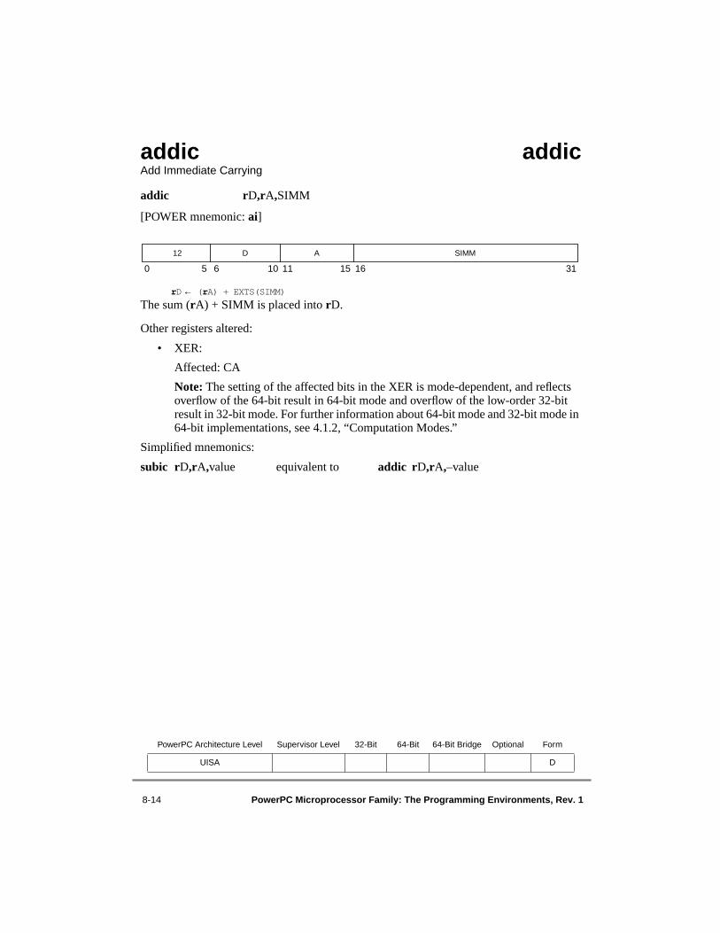
8-14 PowerPC Microprocessor Family: The Programming Environments, Rev. 1
addic addicAdd Immediate Carrying
addic rD,rA,SIMM
[POWER mnemonic: ai]
rD ← (rA) + EXTS(SIMM)
The sum (rA) + SIMM is placed into rD.
Other registers altered:
• XER:
Affected: CA
Note: The setting of the affected bits in the XER is mode-dependent, and reflects overflow of the 64-bit result in 64-bit mode and overflow of the low-order 32-bit result in 32-bit mode. For further information about 64-bit mode and 32-bit mode in 64-bit implementations, see 4.1.2, “Computation Modes.”
Simplified mnemonics:
subic rD,rA,value equivalent to addic rD,rA,–value
PowerPC Architecture Level Supervisor Level 32-Bit 64-Bit 64-Bit Bridge Optional Form
UISA D
0 5 6 10 11 15 16 31
12 D A SIMM
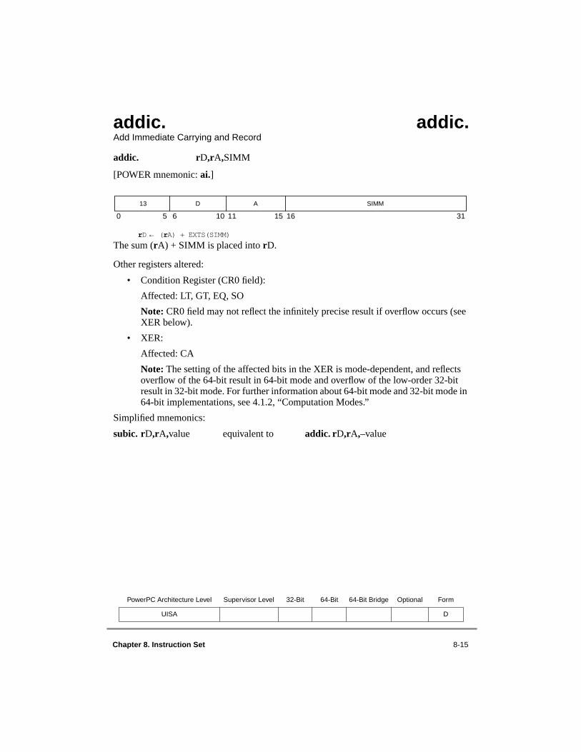
Chapter 8. Instruction Set 8-15
addic. addic.Add Immediate Carrying and Record
addic. rD,rA,SIMM
[POWER mnemonic: ai.]
rD ← (rA) + EXTS(SIMM)
The sum (rA) + SIMM is placed into rD.
Other registers altered:
• Condition Register (CR0 field):
Affected: LT, GT, EQ, SO
Note: CR0 field may not reflect the infinitely precise result if overflow occurs (see XER below).
• XER:
Affected: CA
Note: The setting of the affected bits in the XER is mode-dependent, and reflects overflow of the 64-bit result in 64-bit mode and overflow of the low-order 32-bit result in 32-bit mode. For further information about 64-bit mode and 32-bit mode in 64-bit implementations, see 4.1.2, “Computation Modes.”
Simplified mnemonics:
subic. rD,rA,value equivalent to addic. rD,rA,–value
PowerPC Architecture Level Supervisor Level 32-Bit 64-Bit 64-Bit Bridge Optional Form
UISA D
0 5 6 10 11 15 16 31
13 D A SIMM
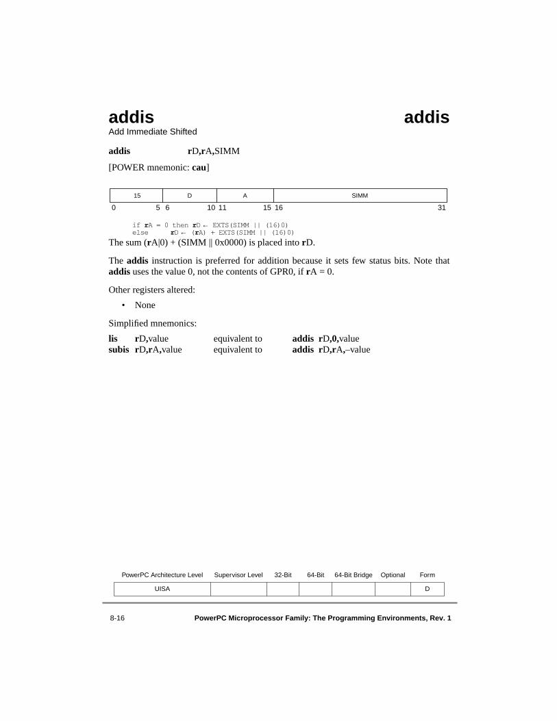
8-16 PowerPC Microprocessor Family: The Programming Environments, Rev. 1
addis addis Add Immediate Shifted
addis rD,rA,SIMM
[POWER mnemonic: cau]
if rA = 0 then rD ← EXTS(SIMM || (16)0)else rD ← (rA) + EXTS(SIMM || (16)0)
The sum (rA|0) + (SIMM || 0x0000) is placed into rD.
The addis instruction is preferred for addition because it sets few status bits. Note thataddis uses the value 0, not the contents of GPR0, if rA = 0.
Other registers altered:
• None
Simplified mnemonics:
lis rD,value equivalent to addis rD,0,valuesubis rD,rA,value equivalent to addis rD,rA,–value
PowerPC Architecture Level Supervisor Level 32-Bit 64-Bit 64-Bit Bridge Optional Form
UISA D
0 5 6 10 11 15 16 31
15 D A SIMM

Chapter 8. Instruction Set 8-17
addmex addmexAdd to Minus One Extended
addme rD,rA (OE = 0 Rc = 0)addme. rD,rA (OE = 0 Rc = 1)addmeo rD,rA (OE = 1 Rc = 0)addmeo. rD,rA (OE = 1 Rc = 1)
[POWER mnemonics: ame, ame., ameo, ameo.]
rD ← (rA) + XER[CA] – 1
The sum (rA) + XER[CA] + 0xFFFF_FFFF_FFFF_FFFF is placed into rD.
Other registers altered:
• Condition Register (CR0 field):
Affected: LT, GT, EQ, SO (if Rc = 1)
Note: CR0 field may not reflect the infinitely precise result if overflow occurs (see XER below).
• XER:
Affected: CA
Affected: SO, OV (if OE = 1)
Note: The setting of the affected bits in the XER is mode-dependent, and reflects overflow of the 64-bit result in 64-bit mode and overflow of the low-order 32-bit result in 32-bit mode. For further information about 64-bit mode and 32-bit mode in 64-bit implementations, see 4.1.2, “Computation Modes.”
PowerPC Architecture Level Supervisor Level 32-Bit 64-Bit 64-Bit Bridge Optional Form
UISA XO
0 5 6 10 11 15 16 20 21 22 30 31
Reserved
31 D A 0 0 0 0 0 OE 234 Rc

8-18 PowerPC Microprocessor Family: The Programming Environments, Rev. 1
addzex addzexAdd to Zero Extended
addze rD,rA (OE = 0 Rc = 0)addze. rD,rA (OE = 0 Rc = 1)addzeo rD,rA (OE = 1 Rc = 0)addzeo. rD,rA (OE = 1 Rc = 1)
[POWER mnemonics: aze, aze., azeo, azeo.]
rD ← (rA) + XER[CA]
The sum (rA) + XER[CA] is placed into rD.
Other registers altered:
• Condition Register (CR0 field):
Affected: LT, GT, EQ, SO (if Rc = 1)
Note: CR0 field may not reflect the infinitely precise result if overflow occurs (see XER below).
• XER:
Affected: CA
Affected: SO, OV (if OE = 1)
Note: The setting of the affected bits in the XER is mode-dependent, and reflects overflow of the 64-bit result in 64-bit mode and overflow of the low-order 32-bit result in 32-bit mode. For further information about 64-bit mode and 32-bit mode in 64-bit implementations, see 4.1.2, “Computation Modes.”
PowerPC Architecture Level Supervisor Level 32-Bit 64-Bit 64-Bit Bridge Optional Form
UISA XO
0 5 6 10 11 15 16 20 21 22 30 31
Reserved
31 D A 0 0 0 0 0 OE 202 Rc

Chapter 8. Instruction Set 8-19
andx andxAND
and rA,rS,rB (Rc = 0)and. rA,rS,rB (Rc = 1)
rA ← (rS) & (rB)
The contents of rS are ANDed with the contents of rB and the result is placed into rA.
Other registers altered:
• Condition Register (CR0 field):
Affected: LT, GT, EQ, SO (if Rc = 1)
PowerPC Architecture Level Supervisor Level 32-Bit 64-Bit 64-Bit Bridge Optional Form
UISA X
0 5 6 10 11 15 16 20 21 30 31
31 S A B 28 Rc
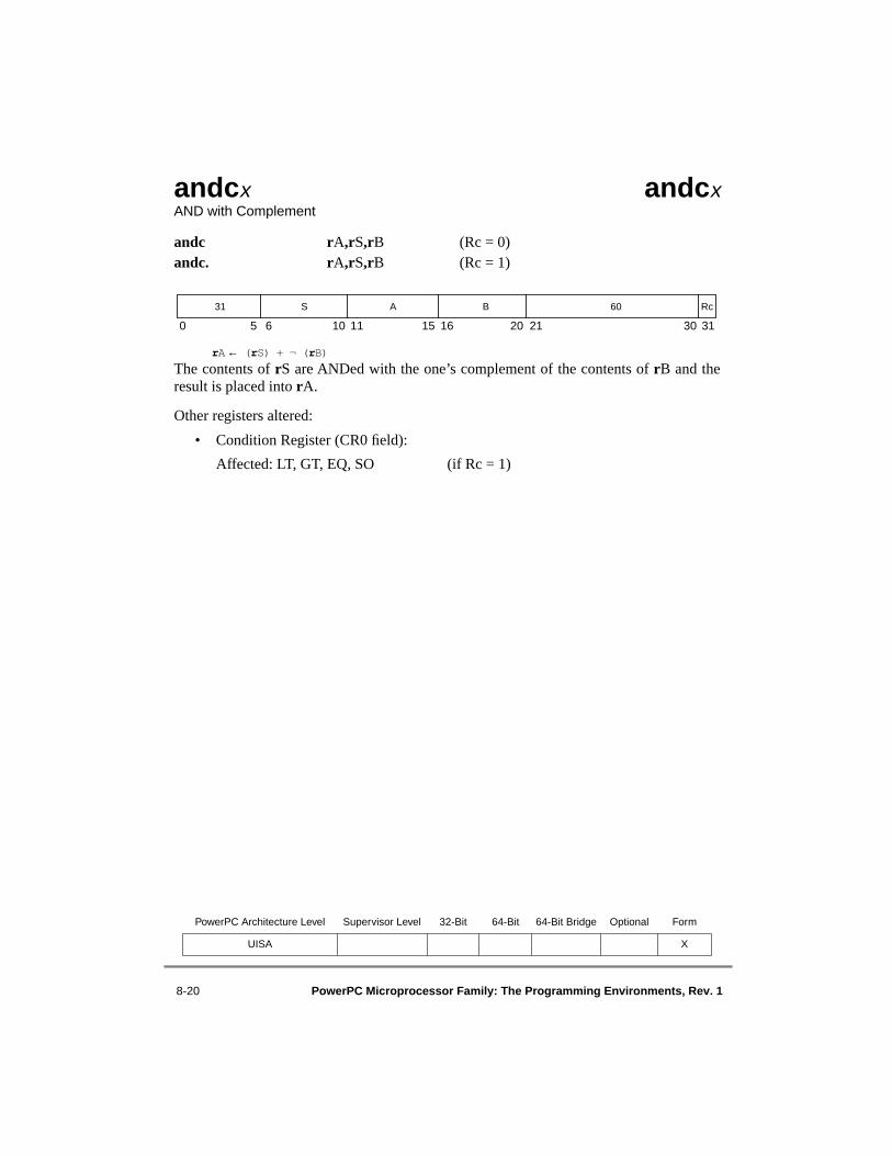
8-20 PowerPC Microprocessor Family: The Programming Environments, Rev. 1
andcx andcxAND with Complement
andc rA,rS,rB (Rc = 0)andc. rA,rS,rB (Rc = 1)
rA ← (rS) + ¬ (rB)
The contents of rS are ANDed with the one’s complement of the contents of rB and theresult is placed into rA.
Other registers altered:
• Condition Register (CR0 field):
Affected: LT, GT, EQ, SO (if Rc = 1)
PowerPC Architecture Level Supervisor Level 32-Bit 64-Bit 64-Bit Bridge Optional Form
UISA X
0 5 6 10 11 15 16 20 21 30 31
31 S A B 60 Rc

Chapter 8. Instruction Set 8-21
andi. andi.AND Immediate
andi. rA,rS,UIMM
[POWER mnemonic: andil.]
rA ← (rS) & ((48)0 || UIMM)
The contents of rS are ANDed with 0x0000_0000_0000 || UIMM and the result is placedinto rA.
Other registers altered:
• Condition Register (CR0 field):
Affected: LT, GT, EQ, SO
PowerPC Architecture Level Supervisor Level 32-Bit 64-Bit 64-Bit Bridge Optional Form
UISA D
0 5 6 10 11 15 16 31
28 S A UIMM

8-22 PowerPC Microprocessor Family: The Programming Environments, Rev. 1
andis. andis. AND Immediate Shifted
andis. rA,rS,UIMM
[POWER mnemonic: andiu.]
rA ← (rS) + ((32)0 || UIMM || (16)0)
The contents of rS are ANDed with 0x0000_0000 || UIMM || 0x0000 and the result isplaced into rA.
Other registers altered:
• Condition Register (CR0 field):
Affected: LT, GT, EQ, SO
PowerPC Architecture Level Supervisor Level 32-Bit 64-Bit 64-Bit Bridge Optional Form
UISA D
0 5 6 10 11 15 16 31
29 S A UIMM

Chapter 8. Instruction Set 8-23
bx bxBranch
b target_addr (AA = 0 LK = 0)ba target_addr (AA = 1 LK = 0)bl target_addr (AA = 0 LK = 1) bla target_addr (AA = 1 LK = 1)
if AA then NIA ←iea EXTS(LI || 0b00)else NIA ←iea CIA + EXTS(LI || 0b00)if LK then LR ←iea CIA + 4
target_addr specifies the branch target address.
If AA = 0, then the branch target address is the sum of LI || 0b00 sign-extended and theaddress of this instruction, with the high-order 32 bits of the branch target address clearedin 32-bit mode of 64-bit implementations.
If AA = 1, then the branch target address is the value LI || 0b00 sign-extended, with the high-order 32 bits of the branch target address cleared in 32-bit mode of 64-bit implementations.
If LK = 1, then the effective address of the instruction following the branch instruction isplaced into the link register.
Other registers altered:
Affected: Link Register (LR) (if LK = 1)
PowerPC Architecture Level Supervisor Level 32-Bit 64-Bit 64-Bit Bridge Optional Form
UISA I
0 5 6 29 30 31
18 LI AA LK
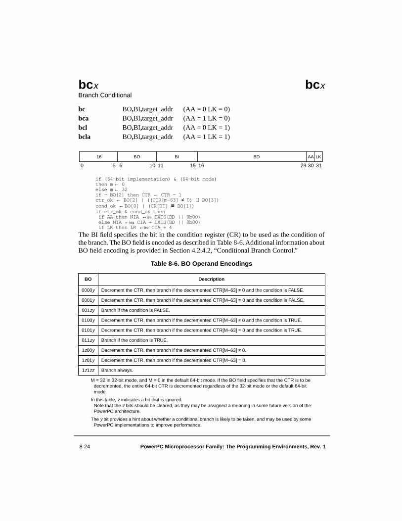
8-24 PowerPC Microprocessor Family: The Programming Environments, Rev. 1
bcx bcxBranch Conditional
bc BO,BI,target_addr (AA = 0 LK = 0)bca BO,BI,target_addr (AA = 1 LK = 0)bcl BO,BI,target_addr (AA = 0 LK = 1)bcla BO,BI,target_addr (AA = 1 LK = 1)
if (64-bit implementation) & (64-bit mode)then m ← 0else m ← 32if ¬ BO[2] then CTR ← CTR – 1ctr_ok ← BO[2] | ((CTR[m–63] ≠ 0) ⊕ BO[3])cond_ok ← BO[0] | (CR[BI] ≡ BO[1])if ctr_ok & cond_ok then if AA then NIA ←iea EXTS(BD || 0b00) else NIA ←iea CIA + EXTS(BD || 0b00) if LK then LR ←iea CIA + 4
The BI field specifies the bit in the condition register (CR) to be used as the condition ofthe branch. The BO field is encoded as described in Table 8-6. Additional information aboutBO field encoding is provided in Section 4.2.4.2, “Conditional Branch Control.”
Table 8-6. BO Operand Encodings
BO Description
0000y Decrement the CTR, then branch if the decremented CTR[M–63] ≠ 0 and the condition is FALSE.
0001y Decrement the CTR, then branch if the decremented CTR[M–63] = 0 and the condition is FALSE.
001zy Branch if the condition is FALSE.
0100y Decrement the CTR, then branch if the decremented CTR[M–63] ≠ 0 and the condition is TRUE.
0101y Decrement the CTR, then branch if the decremented CTR[M–63] = 0 and the condition is TRUE.
011zy Branch if the condition is TRUE.
1z00y Decrement the CTR, then branch if the decremented CTR[M–63] ≠ 0.
1z01y Decrement the CTR, then branch if the decremented CTR[M–63] = 0.
1z1zz Branch always.
M = 32 in 32-bit mode, and M = 0 in the default 64-bit mode. If the BO field specifies that the CTR is to be decremented, the entire 64-bit CTR is decremented regardless of the 32-bit mode or the default 64-bit mode.
In this table, z indicates a bit that is ignored. Note that the z bits should be cleared, as they may be assigned a meaning in some future version of the PowerPC architecture.
The y bit provides a hint about whether a conditional branch is likely to be taken, and may be used by some PowerPC implementations to improve performance.
0 5 6 10 11 15 16 29 30 31
16 BO BI BD AA LK

Chapter 8. Instruction Set 8-25
target_addr specifies the branch target address.
If AA = 0, the branch target address is the sum of BD || 0b00 sign-extended and the addressof this instruction, with the high-order 32 bits of the branch target address cleared in 32-bitmode of 64-bit implementations.
If AA = 1, the branch target address is the value BD || 0b00 sign-extended, with the high-order 32 bits of the branch target address cleared in 32-bit mode of 64-bit implementations.
If LK = 1, the effective address of the instruction following the branch instruction is placedinto the link register.
Other registers altered:
Affected: Count Register (CTR) (if BO[2] = 0)
Affected: Link Register (LR) (if LK = 1)
Simplified mnemonics:
blt target equivalent to bc 12,0,targetbne cr2,target equivalent to bc 4,10,targetbdnz target equivalent to bc 16,0,target
PowerPC Architecture Level Supervisor Level 32-Bit 64-Bit 64-Bit Bridge Optional Form
UISA B
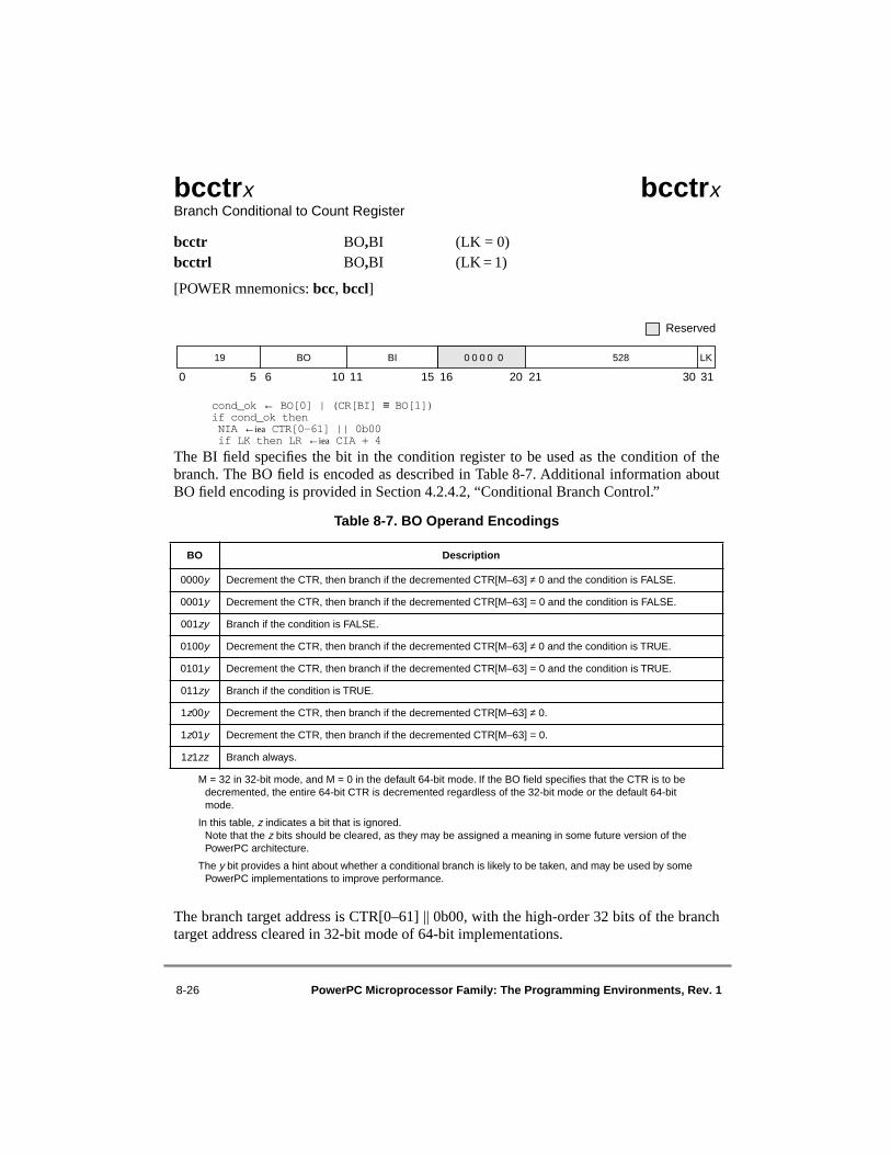
8-26 PowerPC Microprocessor Family: The Programming Environments, Rev. 1
bcctrx bcctrxBranch Conditional to Count Register
bcctr BO,BI (LK = 0)bcctrl BO,BI (LK = 1)
[POWER mnemonics: bcc, bccl]
cond_ok ← BO[0] | (CR[BI] ≡ BO[1])if cond_ok then NIA ←iea CTR[0–61] || 0b00 if LK then LR ←iea CIA + 4
The BI field specifies the bit in the condition register to be used as the condition of thebranch. The BO field is encoded as described in Table 8-7. Additional information aboutBO field encoding is provided in Section 4.2.4.2, “Conditional Branch Control.”
Table 8-7. BO Operand Encodings
The branch target address is CTR[0–61] || 0b00, with the high-order 32 bits of the branchtarget address cleared in 32-bit mode of 64-bit implementations.
BO Description
0000y Decrement the CTR, then branch if the decremented CTR[M–63] ≠ 0 and the condition is FALSE.
0001y Decrement the CTR, then branch if the decremented CTR[M–63] = 0 and the condition is FALSE.
001zy Branch if the condition is FALSE.
0100y Decrement the CTR, then branch if the decremented CTR[M–63] ≠ 0 and the condition is TRUE.
0101y Decrement the CTR, then branch if the decremented CTR[M–63] = 0 and the condition is TRUE.
011zy Branch if the condition is TRUE.
1z00y Decrement the CTR, then branch if the decremented CTR[M–63] ≠ 0.
1z01y Decrement the CTR, then branch if the decremented CTR[M–63] = 0.
1z1zz Branch always.
M = 32 in 32-bit mode, and M = 0 in the default 64-bit mode. If the BO field specifies that the CTR is to be decremented, the entire 64-bit CTR is decremented regardless of the 32-bit mode or the default 64-bit mode.
In this table, z indicates a bit that is ignored. Note that the z bits should be cleared, as they may be assigned a meaning in some future version of the PowerPC architecture.
The y bit provides a hint about whether a conditional branch is likely to be taken, and may be used by some PowerPC implementations to improve performance.
0 5 6 10 11 15 16 20 21 30 31
Reserved
19 BO BI 0 0 0 0 0 528 LK

Chapter 8. Instruction Set 8-27
If LK = 1, the effective address of the instruction following the branch instruction is placedinto the link register.
If the “decrement and test CTR” option is specified (BO[2] = 0), the instruction form isinvalid.
Other registers altered:
Affected: Link Register (LR) (if LK = 1)
Simplified mnemonics:
bltctr equivalent to bcctr 12,0bnectr cr2 equivalent to bcctr 4,10
PowerPC Architecture Level Supervisor Level 32-Bit 64-Bit 64-Bit Bridge Optional Form
UISA XL

8-28 PowerPC Microprocessor Family: The Programming Environments, Rev. 1
bclrx bclrxBranch Conditional to Link Register
bclr BO,BI (LK = 0)bclrl BO,BI (LK = 1)
[POWER mnemonics: bcr, bcrl]
if (64-bit implementation) & (64-bit mode)then m ← 0else m ← 32if ¬ BO[2] then CTR ← CTR – 1ctr_ok ← BO[2] | ((CTR[m–63] ≠ 0) ⊕ BO[3])cond_ok ← BO[0] | (CR[BI] ≡ BO[1])if ctr_ok & cond_ok then NIA ←iea LR[0–61] || 0b00 if LK then LR ←iea CIA + 4
The BI field specifies the bit in the condition register to be used as the condition of thebranch. The BO field is encoded as described in Table 8-8. Additional information aboutBO field encoding is provided in Section 4.2.4.2, “Conditional Branch Control.”
Table 8-8. BO Operand Encodings
BO Description
0000y Decrement the CTR, then branch if the decremented CTR[M–63] ≠ 0 and the condition is FALSE.
0001y Decrement the CTR, then branch if the decremented CTR[M–63] = 0 and the condition is FALSE.
001zy Branch if the condition is FALSE.
0100y Decrement the CTR, then branch if the decremented CTR[M–63] ≠ 0 and the condition is TRUE.
0101y Decrement the CTR, then branch if the decremented CTR[M–63] = 0 and the condition is TRUE.
011zy Branch if the condition is TRUE.
1z00y Decrement the CTR, then branch if the decremented CTR[M–63] ≠ 0.
1z01y Decrement the CTR, then branch if the decremented CTR[M–63] = 0.
1z1zz Branch always.
M = 32 in 32-bit mode, and M = 0 in the default 64-bit mode. If the BO field specifies that the CTR is to be decremented, the entire 64-bit CTR is decremented regardless of the 32-bit mode or the default 64-bit mode.
In this table, z indicates a bit that is ignored. Note that the z bits should be cleared, as they may be assigned a meaning in some future version of the PowerPC architecture.
The y bit provides a hint about whether a conditional branch is likely to be taken, and may be used by some PowerPC implementations to improve performance.
0 5 6 10 11 15 16 20 21 30 31
Reserved
19 BO BI 0 0 0 0 0 16 LK

Chapter 8. Instruction Set 8-29
The branch target address is LR[0–61] || 0b00, with the high-order 32 bits of the branchtarget address cleared in 32-bit mode of 64-bit implementations.
If LK = 1, then the effective address of the instruction following the branch instruction isplaced into the link register.
Other registers altered:
Affected: Count Register (CTR) (if BO[2] = 0)
Affected: Link Register (LR) (if LK = 1)
Simplified mnemonics:
bltlr equivalent to bclr 12,0bnelr cr2 equivalent to bclr 4,10 bdnzlr equivalent to bclr 16,0
PowerPC Architecture Level Supervisor Level 32-Bit 64-Bit 64-Bit Bridge Optional Form
UISA XL

8-30 PowerPC Microprocessor Family: The Programming Environments, Rev. 1
cmp cmp Compare
cmp crfD,L,rA,rB
if L = 0 then a ← EXTS(rA[32–63])b ← EXTS(rB[32–63])
else a ← (rA)b ← (rB)
if a < b then c ← 0b100else if a > b then c ← 0b010else c ← 0b001CR[4 ∗ crfD–4 ∗ crfD + 3] ← c || XER[SO]
The contents of rA (or the low-order 32 bits of rA if L = 0) are compared with the contentsof rB (or the low-order 32 bits of rB if L = 0), treating the operands as signed integers. Theresult of the comparison is placed into CR field crfD.
In 32-bit implementations, if L = 1 the instruction form is invalid.
Other registers altered:
• Condition Register (CR field specified by operand crfD):
Affected: LT, GT, EQ, SO
Simplified mnemonics:
cmpd rA,rB equivalent to cmp 0,1,rA,rBcmpw cr3,rA,rB equivalent to cmp 3,0,rA,rB
PowerPC Architecture Level Supervisor Level 32-Bit 64-Bit 64-Bit Bridge Optional Form
UISA X
0 5 6 8 9 10 11 15 16 20 21 30 31
Reserved
B 0 0 0 0 0 0 0 0 0 0 031 crfD 0 L A

Chapter 8. Instruction Set 8-31
cmpi cmpiCompare Immediate
cmpi crfD,L,rA,SIMM
if L = 0 then a ← EXTS(rA[32–63])elsea ← (rA)
if a < EXTS(SIMM) then c ← 0b100else if a > EXTS(SIMM) then c ← 0b010else c ← 0b001CR[4 ∗ crfD–4 ∗ crfD + 3] ← c || XER[SO]
The contents of rA (or the low-order 32 bits of rA sign-extended to 64 bits if L = 0) arecompared with the sign-extended value of the SIMM field, treating the operands as signedintegers. The result of the comparison is placed into CR field crfD.
In 32-bit implementations, if L = 1 the instruction form is invalid.
Other registers altered:
• Condition Register (CR field specified by operand crfD):
Affected: LT, GT, EQ, SO
Simplified mnemonics:
cmpdirA,value equivalent to cmpi 0,1,rA,valuecmpwi cr3,rA,value equivalent to cmpi 3,0,rA,value
PowerPC Architecture Level Supervisor Level 32-Bit 64-Bit 64-Bit Bridge Optional Form
UISA D
0 5 6 8 9 10 11 15 16 31
Reserved
SIMM11 crfD 0 L A

8-32 PowerPC Microprocessor Family: The Programming Environments, Rev. 1
cmpl cmplCompare Logical
cmpl crfD,L,rA,rB
if L = 0 then a ← (32)0 || rA[32–63]b ← (32)0 || rB[32–63]
elsea ← (rA)b ← (rB)
if a <U b then c ← 0b100else if a >U b then c ← 0b010else c ← 0b001CR[4 ∗ crfD–4 ∗ crfD + 3] ← c || XER[SO]
The contents of rA (or the low-order 32 bits of rA if L = 0) are compared with the contentsof rB (or the low-order 32 bits of rB if L = 0), treating the operands as unsigned integers.The result of the comparison is placed into CR field crfD.
In 32-bit implementations, if L = 1 the instruction form is invalid.
Other registers altered:
• Condition Register (CR field specified by operand crfD):
Affected: LT, GT, EQ, SO
Simplified mnemonics:
cmpldrA,rB equivalent to cmpl 0,1,rA,rBcmplw cr3,rA,rB equivalent to cmpl 3,0,rA,rB
PowerPC Architecture Level Supervisor Level 32-Bit 64-Bit 64-Bit Bridge Optional Form
UISA X
0 5 6 8 9 10 11 15 16 20 21 31
Reserved
31 crfD 0 L A B 32 0

Chapter 8. Instruction Set 8-33
cmpli cmpli Compare Logical Immediate
cmpli crfD,L,rA,UIMM
if L = 0 then a ← (32)0 || rA[32–63]else a ← (rA)
if a <U ((48)0 || UIMM) then c ← 0b100else if a >U ((48)0 || UIMM) then c ← 0b010else c ← 0b001CR[4 ∗ crfD–4 ∗ crfD + 3] ← c || XER[SO]
The contents of rA (or the low-order 32 bits of rA zero-extended to 64-bits if L = 0) arecompared with 0x0000_0000_0000 || UIMM, treating the operands as unsigned integers.The result of the comparison is placed into CR field crfD.
In 32-bit implementations, if L = 1 the instruction form is invalid.
Other registers altered:
• Condition Register (CR field specified by operand crfD):
Affected: LT, GT, EQ, SO
Simplified mnemonics:
cmpldir A,value equivalent to cmpli 0,1,rA,valuecmplwi cr3,rA,value equivalent to cmpli 3,0,rA,value
PowerPC Architecture Level Supervisor Level 32-Bit 64-Bit 64-Bit Bridge Optional Form
UISA D
0 5 6 8 9 10 11 15 16 31
Reserved
UIMM10 crfD 0 L A
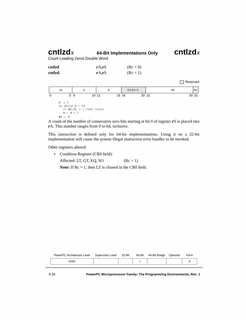
8-34 PowerPC Microprocessor Family: The Programming Environments, Rev. 1
cntlzdx 64-Bit Implementations Only cntlzdxCount Leading Zeros Double Word
cntlzd rA,rS (Rc = 0)cntlzd. rA,rS (Rc = 1)
n ← 0do while n < 64
if rS[n] = 1 then leaven ← n + 1
rA ← n
A count of the number of consecutive zero bits starting at bit 0 of register rS is placed intorA. This number ranges from 0 to 64, inclusive.
This instruction is defined only for 64-bit implementations. Using it on a 32-bitimplementation will cause the system illegal instruction error handler to be invoked.
Other registers altered:
• Condition Register (CR0 field):
Affected: LT, GT, EQ, SO (Rc = 1)
Note: If Rc = 1, then LT is cleared in the CR0 field.
PowerPC Architecture Level Supervisor Level 32-Bit 64-Bit 64-Bit Bridge Optional Form
UISA √ X
0 5 6 10 11 15 16 20 21 30 31
Reserved
31 S A 0 0 0 0 0 58 Rc

Chapter 8. Instruction Set 8-35
cntlzwx cntlzwxCount Leading Zeros Word
cntlzw rA,rS (Rc = 0)cntlzw. rA,rS (Rc = 1)
[POWER mnemonics: cntlz, cntlz.]
n ← 32do while n < 64if rS[n] = 1 then leaven ← n + 1rA ← n – 32
A count of the number of consecutive zero bits starting at bit 32 of rS (bit 0 in 32-bitimplementations) is placed into rA. This number ranges from 0 to 32, inclusive.
Other registers altered:
• Condition Register (CR0 field):
Affected: LT, GT, EQ, SO (if Rc = 1)
Note: If Rc = 1, then LT is cleared in the CR0 field.
PowerPC Architecture Level Supervisor Level 32-Bit 64-Bit 64-Bit Bridge Optional Form
UISA X
0 5 6 10 11 15 16 20 21 30 31
Reserved
31 S A 0 0 0 0 0 26 Rc

8-36 PowerPC Microprocessor Family: The Programming Environments, Rev. 1
crand crandCondition Register AND
crand crbD,crbA,crbB
CR[crbD] ← CR[crbA] & CR[crbB]
The bit in the condition register specified by crbA is ANDed with the bit in the conditionregister specified by crbB. The result is placed into the condition register bit specified bycrbD.
Other registers altered:
• Condition Register:
Affected: Bit specified by operand crbD
PowerPC Architecture Level Supervisor Level 32-Bit 64-Bit 64-Bit Bridge Optional Form
UISA XL
0 5 6 10 11 15 16 20 21 30 31
Reserved
19 crbD crbA crbB 257 0

Chapter 8. Instruction Set 8-37
crandc crandcCondition Register AND with Complement
crandc crbD,crbA,crbB
CR[crbD] ← CR[crbA] & ¬ CR[crbB]
The bit in the condition register specified by crbA is ANDed with the complement of thebit in the condition register specified by crbB and the result is placed into the conditionregister bit specified by crbD.
Other registers altered:
• Condition Register:
Affected: Bit specified by operand crbD
PowerPC Architecture Level Supervisor Level 32-Bit 64-Bit 64-Bit Bridge Optional Form
UISA XL
0 5 6 10 11 15 16 20 21 30 31
Reserved
19 crbD crbA crbB 129 0
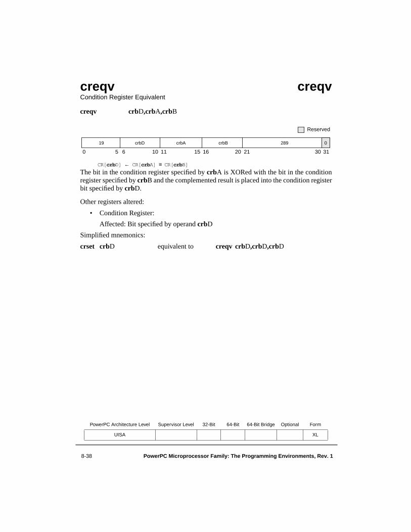
8-38 PowerPC Microprocessor Family: The Programming Environments, Rev. 1
creqv creqvCondition Register Equivalent
creqv crbD,crbA,crbB
CR[crbD] ← CR[crbA] ≡ CR[crbB]The bit in the condition register specified by crbA is XORed with the bit in the conditionregister specified by crbB and the complemented result is placed into the condition registerbit specified by crbD.
Other registers altered:
• Condition Register:
Affected: Bit specified by operand crbD
Simplified mnemonics:
crset crbD equivalent to creqv crbD,crbD,crbD
PowerPC Architecture Level Supervisor Level 32-Bit 64-Bit 64-Bit Bridge Optional Form
UISA XL
0 5 6 10 11 15 16 20 21 30 31
Reserved
19 crbD crbA crbB 289 0

Chapter 8. Instruction Set 8-39
crnand crnandCondition Register NAND
crnand crbD,crbA,crbB
CR[crbD] ← ¬ (CR[crbA] & CR[crbB])
The bit in the condition register specified by crbA is ANDed with the bit in the conditionregister specified by crbB and the complemented result is placed into the condition registerbit specified by crbD.
Other registers altered:
• Condition Register:
Affected: Bit specified by operand crbD
PowerPC Architecture Level Supervisor Level 32-Bit 64-Bit 64-Bit Bridge Optional Form
UISA XL
0 5 6 10 11 15 16 20 21 30 31
Reserved
19 crbD crbA crbB 225 0

8-40 PowerPC Microprocessor Family: The Programming Environments, Rev. 1
crnor crnorCondition Register NOR
crnor crbD,crbA,crbB
CR[crbD] ← ¬ (CR[crbA] | CR[crbB])
The bit in the condition register specified by crbA is ORed with the bit in the conditionregister specified by crbB and the complemented result is placed into the condition registerbit specified by crbD.
Other registers altered:
• Condition Register:
Affected: Bit specified by operand crbD
Simplified mnemonics:
crnot crbD,crbA equivalent to crnor crbD,crbA,crbA
PowerPC Architecture Level Supervisor Level 32-Bit 64-Bit 64-Bit Bridge Optional Form
UISA XL
0 5 6 10 11 15 16 20 21 30 31
Reserved
19 crbD crbA crbB 33 0

Chapter 8. Instruction Set 8-41
cror crorCondition Register OR
cror crbD,crbA,crbB
CR[crbD] ← CR[crbA] | CR[crbB]
The bit in the condition register specified by crbA is ORed with the bit in the conditionregister specified by crbB. The result is placed into the condition register bit specified bycrbD.
Other registers altered:
• Condition Register:
Affected: Bit specified by operand crbD
Simplified mnemonics:
crmove crbD,crbA equivalent to cror crbD,crbA,crbA
PowerPC Architecture Level Supervisor Level 32-Bit 64-Bit 64-Bit Bridge Optional Form
UISA XL
0 5 6 10 11 15 16 20 21 30 31
Reserved
19 crbD crbA crbB 449 0

8-42 PowerPC Microprocessor Family: The Programming Environments, Rev. 1
crorc crorcCondition Register OR with Complement
crorc crbD,crbA,crbB
CR[crbD] ← CR[crbA] | ¬ CR[crbB]
The bit in the condition register specified by crbA is ORed with the complement of thecondition register bit specified by crbB and the result is placed into the condition registerbit specified by crbD.
Other registers altered:
• Condition Register:
Affected: Bit specified by operand crbD
PowerPC Architecture Level Supervisor Level 32-Bit 64-Bit 64-Bit Bridge Optional Form
UISA XL
0 5 6 10 11 15 16 20 21 30 31
Reserved
19 crbD crbA crbB 417 0

Chapter 8. Instruction Set 8-43
crxor crxorCondition Register XOR
crxor crbD,crbA,crbB
CR[crbD] ← CR[crbA] ⊕ CR[crbB]The bit in the condition register specified by crbA is XORed with the bit in the conditionregister specified by crbB and the result is placed into the condition register specified bycrbD.
Other registers altered:
• Condition Register:
Affected: Bit specified by crbD
Simplified mnemonics:
crclr crbD equivalent to crxor crbD,crbD,crbD
PowerPC Architecture Level Supervisor Level 32-Bit 64-Bit 64-Bit Bridge Optional Form
UISA XL
0 5 6 10 11 15 16 20 21 30 31
Reserved
19 crbD crbA crbB 193 0
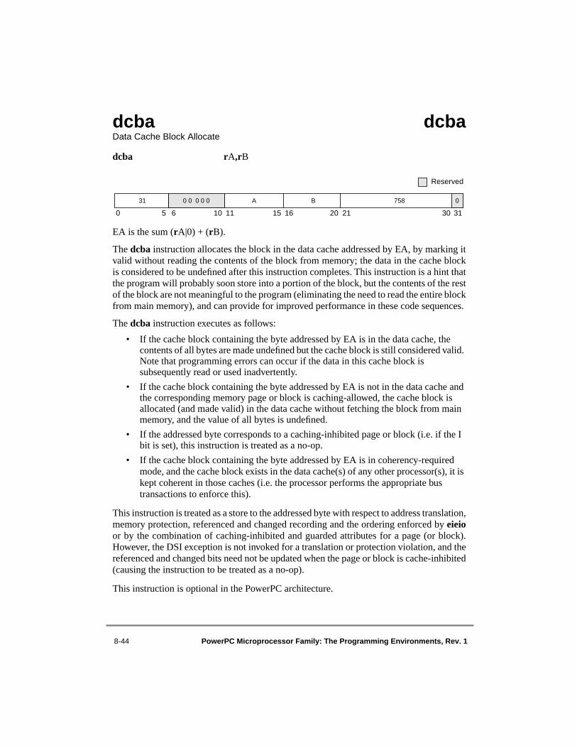
8-44 PowerPC Microprocessor Family: The Programming Environments, Rev. 1
dcba dcbaData Cache Block Allocate
dcba rA,rB
EA is the sum (rA|0) + (rB).
The dcba instruction allocates the block in the data cache addressed by EA, by marking itvalid without reading the contents of the block from memory; the data in the cache blockis considered to be undefined after this instruction completes. This instruction is a hint thatthe program will probably soon store into a portion of the block, but the contents of the restof the block are not meaningful to the program (eliminating the need to read the entire blockfrom main memory), and can provide for improved performance in these code sequences.
The dcba instruction executes as follows:
• If the cache block containing the byte addressed by EA is in the data cache, the contents of all bytes are made undefined but the cache block is still considered valid. Note that programming errors can occur if the data in this cache block is subsequently read or used inadvertently.
• If the cache block containing the byte addressed by EA is not in the data cache and the corresponding memory page or block is caching-allowed, the cache block is allocated (and made valid) in the data cache without fetching the block from main memory, and the value of all bytes is undefined.
• If the addressed byte corresponds to a caching-inhibited page or block (i.e. if the I bit is set), this instruction is treated as a no-op.
• If the cache block containing the byte addressed by EA is in coherency-required mode, and the cache block exists in the data cache(s) of any other processor(s), it is kept coherent in those caches (i.e. the processor performs the appropriate bus transactions to enforce this).
This instruction is treated as a store to the addressed byte with respect to address translation,memory protection, referenced and changed recording and the ordering enforced by eieioor by the combination of caching-inhibited and guarded attributes for a page (or block).However, the DSI exception is not invoked for a translation or protection violation, and thereferenced and changed bits need not be updated when the page or block is cache-inhibited(causing the instruction to be treated as a no-op).
This instruction is optional in the PowerPC architecture.
0 5 6 10 11 15 16 20 21 30 31
Reserved
B 758 031 0 0 0 0 0 A

Chapter 8. Instruction Set 8-45
Other registers altered:
• None
In the PowerPC OEA, the dcba instruction is additionally defined to clear all bytes of anewly established block to zero in the case that the block did not already exist in the cache.
Additionally, as the dcba instruction may establish a block in the data cache withoutverifying that the associated physical address is valid, a delayed machine check exceptionis possible. See Chapter 6, “Exceptions,” for a discussion about this type of machine checkexception.
PowerPC Architecture Level Supervisor Level 32-Bit 64-Bit 64-Bit Bridge Optional Form
VEA √ X

8-46 PowerPC Microprocessor Family: The Programming Environments, Rev. 1
dcbf dcbfData Cache Block Flush
dcbf rA,rB
EA is the sum (rA|0) + (rB).
The dcbf instruction invalidates the block in the data cache addressed by EA, copying theblock to memory first, if there is any dirty data in it. If the processor is a multiprocessorimplementation (for example, the 601, 604, 604e and 620) and the block is markedcoherency-required, the processor will, if necessary, send an address-only broadcast toother processors. The broadcast of the dcbf instruction causes another processor to copythe block to memory, if it has dirty data, and then invalidate the block from the cache.
The action taken depends on the memory mode associated with the block containing thebyte addressed by EA and on the state of that block. The list below describes the actiontaken for the various states of the memory coherency attribute (M bit).
• Coherency required
— Unmodified block—Invalidates copies of the block in the data caches of all processors.
— Modified block—Copies the block to memory. Invalidates copies of the block in the data caches of all processors.
— Absent block—If modified copies of the block are in the data caches of other processors, causes them to be copied to memory and invalidated in those data caches. If unmodified copies are in the data caches of other processors, causes those copies to be invalidated in those data caches.
• Coherency not required
— Unmodified block—Invalidates the block in the processor’s data cache.— Modified block—Copies the block to memory. Invalidates the block in the
processor’s data cache.— Absent block (target block not in cache)—No action is taken.
The function of this instruction is independent of the write-through, write-back andcaching-inhibited/allowed modes of the block containing the byte addressed by EA.
0 5 6 10 11 15 16 20 21 30 31
Reserved
B 86 031 0 0 0 0 0 A

Chapter 8. Instruction Set 8-47
This instruction is treated as a load from the addressed byte with respect to addresstranslation and memory protection. It is also treated as a load for referenced and changedbit recording except that referenced and changed bit recording may not occur.
Other registers altered:
• None
PowerPC Architecture Level Supervisor Level 32-Bit 64-Bit 64-Bit Bridge Optional Form
VEA X

8-48 PowerPC Microprocessor Family: The Programming Environments, Rev. 1
dcbi dcbi Data Cache Block Invalidate
dcbi rA,rB
EA is the sum (rA|0) + (rB).
The action taken is dependent on the memory mode associated with the block containingthe byte addressed by EA and on the state of that block. The list below describes the actiontaken if the block containing the byte addressed by EA is or is not in the cache.
• Coherency required
— Unmodified block—Invalidates copies of the block in the data caches of all processors.
— Modified block—Invalidates copies of the block in the data caches of all processors. (Discards the modified contents.)
— Absent block—If copies of the block are in the data caches of any other processor, causes the copies to be invalidated in those data caches. (Discards any modified contents.)
• Coherency not required
— Unmodified block—Invalidates the block in the processor’s data cache.— Modified block—Invalidates the block in the processor’s data cache. (Discards
the modified contents.)— Absent block (target block not in cache)—No action is taken.
When data address translation is enabled, MSR[DR] = 1, and the virtual address has notranslation, a DSI exception occurs.
The function of this instruction is independent of the write-through and caching-inhibited/allowed modes of the block containing the byte addressed by EA. This instructionoperates as a store to the addressed byte with respect to address translation and protection.The referenced and changed bits are modified appropriately.
This is a supervisor-level instruction.
Other registers altered: • None
PowerPC Architecture Level Supervisor Level 32-Bit 64-Bit 64-Bit Bridge Optional Form
OEA √ X
0 5 6 10 11 15 16 20 21 30 31
Reserved
B 470 031 0 0 0 0 0 A
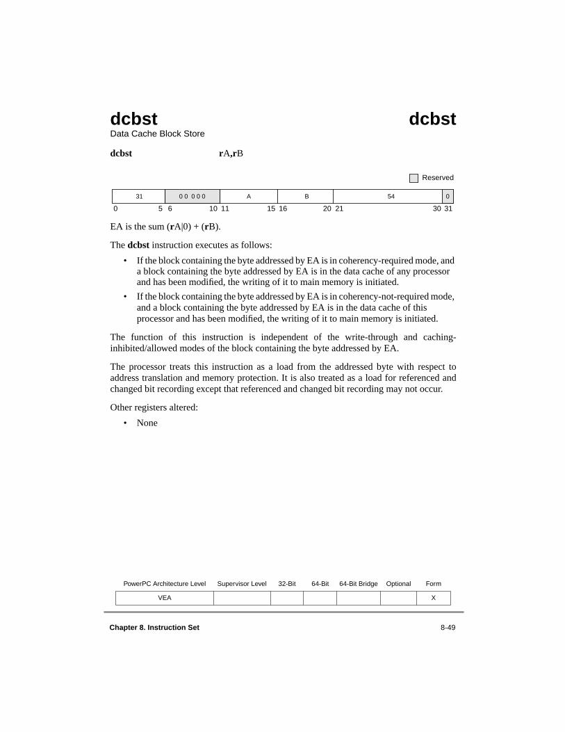
Chapter 8. Instruction Set 8-49
dcbst dcbstData Cache Block Store
dcbst rA,rB
EA is the sum (rA|0) + (rB).
The dcbst instruction executes as follows:
• If the block containing the byte addressed by EA is in coherency-required mode, and a block containing the byte addressed by EA is in the data cache of any processor and has been modified, the writing of it to main memory is initiated.
• If the block containing the byte addressed by EA is in coherency-not-required mode, and a block containing the byte addressed by EA is in the data cache of this processor and has been modified, the writing of it to main memory is initiated.
The function of this instruction is independent of the write-through and caching-inhibited/allowed modes of the block containing the byte addressed by EA.
The processor treats this instruction as a load from the addressed byte with respect toaddress translation and memory protection. It is also treated as a load for referenced andchanged bit recording except that referenced and changed bit recording may not occur.
Other registers altered:
• None
PowerPC Architecture Level Supervisor Level 32-Bit 64-Bit 64-Bit Bridge Optional Form
VEA X
0 5 6 10 11 15 16 20 21 30 31
Reserved
B 54 031 0 0 0 0 0 A
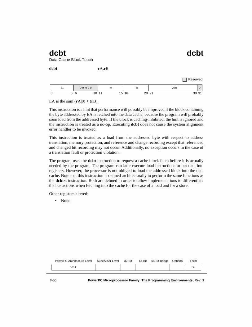
8-50 PowerPC Microprocessor Family: The Programming Environments, Rev. 1
dcbt dcbtData Cache Block Touch
dcbt rA,rB
EA is the sum (rA|0) + (rB).
This instruction is a hint that performance will possibly be improved if the block containingthe byte addressed by EA is fetched into the data cache, because the program will probablysoon load from the addressed byte. If the block is caching-inhibited, the hint is ignored andthe instruction is treated as a no-op. Executing dcbt does not cause the system alignmenterror handler to be invoked.
This instruction is treated as a load from the addressed byte with respect to addresstranslation, memory protection, and reference and change recording except that referencedand changed bit recording may not occur. Additionally, no exception occurs in the case ofa translation fault or protection violation.
The program uses the dcbt instruction to request a cache block fetch before it is actuallyneeded by the program. The program can later execute load instructions to put data intoregisters. However, the processor is not obliged to load the addressed block into the datacache. Note that this instruction is defined architecturally to perform the same functions asthe dcbtst instruction. Both are defined in order to allow implementations to differentiatethe bus actions when fetching into the cache for the case of a load and for a store.
Other registers altered:
• None
PowerPC Architecture Level Supervisor Level 32-Bit 64-Bit 64-Bit Bridge Optional Form
VEA X
0 5 6 10 11 15 16 20 21 30 31
Reserved
B 278 031 0 0 0 0 0 A

Chapter 8. Instruction Set 8-51
dcbtst dcbtstData Cache Block Touch for Store
dcbtst rA,rB
EA is the sum (rA|0) + (rB).
This instruction is a hint that performance will possibly be improved if the block containingthe byte addressed by EA is fetched into the data cache, because the program will probablysoon store from the addressed byte. If the block is caching-inhibited, the hint is ignored andthe instruction is treated as a no-op. Executing dcbtst does not cause the system alignmenterror handler to be invoked.
This instruction is treated as a load from the addressed byte with respect to addresstranslation, memory protection, and reference and change recording except that referencedand changed bit recording may not occur. Additionally, no exception occurs in the case ofa translation fault or protection violation.
The program uses dcbtst to request a cache block fetch to potentially improve performancefor a subsequent store to that EA, as that store would then be to a cached location. However,the processor is not obliged to load the addressed block into the data cache. Note that thisinstruction is defined architecturally to perform the same functions as the dcbt instruction.Both are defined in order to allow implementations to differentiate the bus actions whenfetching into the cache for the case of a load and for a store.
Other registers altered:
• None
PowerPC Architecture Level Supervisor Level 32-Bit 64-Bit 64-Bit Bridge Optional Form
VEA X
0 5 6 10 11 15 16 20 21 30 31
Reserved
B 246 031 0 0 0 0 0 A

8-52 PowerPC Microprocessor Family: The Programming Environments, Rev. 1
dcbz dcbzData Cache Block Clear to Zero
dcbz rA,rB
[POWER mnemonic: dclz]
EA is the sum (rA|0) + (rB).
The dcbz instruction executes as follows:
• If the cache block containing the byte addressed by EA is in the data cache, all bytes are cleared.
• If the cache block containing the byte addressed by EA is not in the data cache and the corresponding memory page or block is caching-allowed, the cache block is allocated (and made valid) in the data cache without fetching the block from main memory, and all bytes are cleared.
• If the page containing the byte addressed by EA is in caching-inhibited or write-through mode, either all bytes of main memory that correspond to the addressed cache block are cleared or the alignment exception handler is invoked. The exception handler can then clear all bytes in main memory that correspond to the addressed cache block.
• If the cache block containing the byte addressed by EA is in coherency-required mode, and the cache block exists in the data cache(s) of any other processor(s), it is kept coherent in those caches (i.e. the processor performs the appropriate bus transactions to enforce this).
This instruction is treated as a store to the addressed byte with respect to address translation,memory protection, referenced and changed recording. It is also treated as a store withrespect to the ordering enforced by eieio and the ordering enforced by the combination ofcaching-inhibited and guarded attributes for a page (or block).
Other registers altered:
• None
0 5 6 10 11 15 16 20 21 30 31
Reserved
B 1014 031 0 0 0 0 0 A

Chapter 8. Instruction Set 8-53
The PowerPC OEA describes how the dcbz instruction may establish a block in the datacache without verifying that the associated physical address is valid. This scenario cancause a delayed machine check exception; see Chapter 6, “Exceptions,” for a discussionabout this type of machine check exception.
PowerPC Architecture Level Supervisor Level 32-Bit 64-Bit 64-Bit Bridge Optional Form
VEA X
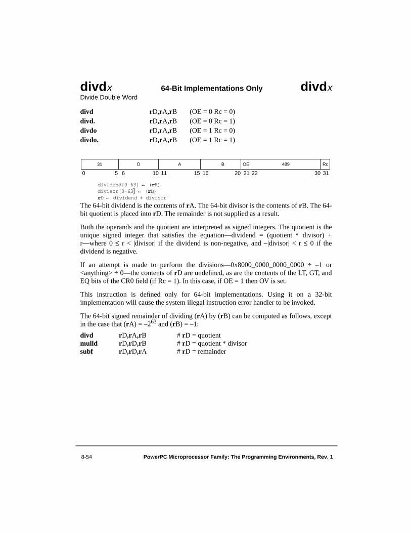
8-54 PowerPC Microprocessor Family: The Programming Environments, Rev. 1
divdx 64-Bit Implementations Only divdxDivide Double Word
divd rD,rA,rB (OE = 0 Rc = 0)divd. rD,rA,rB (OE = 0 Rc = 1)divdo rD,rA,rB (OE = 1 Rc = 0)divdo. rD,rA,rB (OE = 1 Rc = 1)
dividend[0–63] ← (rA)divisor[0–63] ← (rB)rD ← dividend + divisor
The 64-bit dividend is the contents of rA. The 64-bit divisor is the contents of rB. The 64-bit quotient is placed into rD. The remainder is not supplied as a result.
Both the operands and the quotient are interpreted as signed integers. The quotient is theunique signed integer that satisfies the equation—dividend = (quotient ∗ divisor) +r—where 0 ≤ r < |divisor| if the dividend is non-negative, and –|divisor| < r ≤ 0 if thedividend is negative.
If an attempt is made to perform the divisions—0x8000_0000_0000_0000 ÷ –1 or<anything> ÷ 0—the contents of rD are undefined, as are the contents of the LT, GT, andEQ bits of the CR0 field (if Rc = 1). In this case, if OE = 1 then OV is set.
This instruction is defined only for 64-bit implementations. Using it on a 32-bitimplementation will cause the system illegal instruction error handler to be invoked.
The 64-bit signed remainder of dividing (rA) by (rB) can be computed as follows, exceptin the case that (rA) = –263 and (rB) = –1:
divd rD,rA,rB # rD = quotientmulld rD,rD,rB # rD = quotient * divisorsubf rD,rD,rA # rD = remainder
0 5 6 10 11 15 16 20 21 22 30 31
31 D A B OE 489 Rc
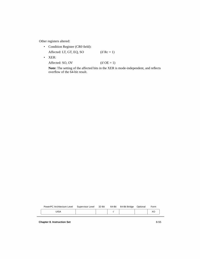
Chapter 8. Instruction Set 8-55
Other registers altered:
• Condition Register (CR0 field):
Affected: LT, GT, EQ, SO (if Rc = 1)
• XER:
Affected: SO, OV (if OE = 1)
Note: The setting of the affected bits in the XER is mode-independent, and reflects overflow of the 64-bit result.
PowerPC Architecture Level Supervisor Level 32-Bit 64-Bit 64-Bit Bridge Optional Form
UISA √ XO

8-56 PowerPC Microprocessor Family: The Programming Environments, Rev. 1
divdux 64-Bit Implementations Only divduxDivide Double Word Unsigned
divdu rD,rA,rB (OE = 0 Rc = 0)divdu. rD,rA,rB (OE = 0 Rc = 1)divduo rD,rA,rB (OE = 1 Rc = 0)divduo. rD,rA,rB (OE = 1 Rc = 1)
dividend[0–63] ← (rA)divisor[0–63] ← (rB)rD ← dividend + divisor
The 64-bit dividend is the contents of rA. The 64-bit divisor is the contents of rB. The 64-bit quotient of the dividend and divisor is placed into rD. The remainder is not supplied asa result.
Both the operands and the quotient are interpreted as unsigned integers, except that if Rc isset to 1 the first three bits of CR0 field are set by signed comparison of the result to zero.The quotient is the unique unsigned integer that satisfies the equation—dividend =(quotient ∗ divisor) + r—where 0 ≤ r < divisor.
If an attempt is made to perform the division—<anything> ÷ 0—the contents of rD areundefined as are the contents of the LT, GT, and EQ bits of the CR0 field (if Rc = 1). In thiscase, if OE = 1 then OV is set.
This instruction is defined only for 64-bit implementations. Using it on a 32-bitimplementation will cause the system illegal instruction error handler to be invoked.
The 64-bit unsigned remainder of dividing (rA) by (rB) can be computed as follows:
divdu rD,rA,rB # rD = quotientmulld rD,rD,rB # rD = quotient * divisorsubf rD,rD,rA # rD = remainder
0 5 6 10 11 15 16 20 21 22 30 31
31 D A B OE 457 Rc

Chapter 8. Instruction Set 8-57
Other registers altered:
• Condition Register (CR0 field):
Affected: LT, GT, EQ, SO (if Rc = 1)
• XER:
Affected: SO, OV (if OE = 1)
Note: The setting of the affected bits in the XER is mode-independent, and reflects overflow of the 64-bit result.
PowerPC Architecture Level Supervisor Level 32-Bit 64-Bit 64-Bit Bridge Optional Form
UISA √ XO
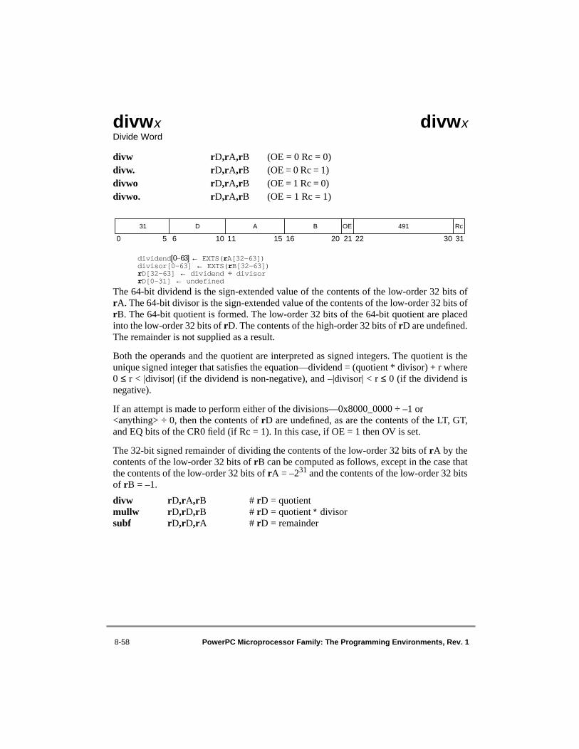
8-58 PowerPC Microprocessor Family: The Programming Environments, Rev. 1
divwx divwxDivide Word
divw rD,rA,rB (OE = 0 Rc = 0)divw. rD,rA,rB (OE = 0 Rc = 1) divwo rD,rA,rB (OE = 1 Rc = 0) divwo. rD,rA,rB (OE = 1 Rc = 1)
dividend[0–63] ← EXTS(rA[32–63])divisor[0–63] ← EXTS(rB[32–63])rD[32–63] ← dividend ÷ divisorrD[0–31] ← undefined
The 64-bit dividend is the sign-extended value of the contents of the low-order 32 bits ofrA. The 64-bit divisor is the sign-extended value of the contents of the low-order 32 bits ofrB. The 64-bit quotient is formed. The low-order 32 bits of the 64-bit quotient are placedinto the low-order 32 bits of rD. The contents of the high-order 32 bits of rD are undefined.The remainder is not supplied as a result.
Both the operands and the quotient are interpreted as signed integers. The quotient is theunique signed integer that satisfies the equation—dividend = (quotient * divisor) + r where0 ≤ r < |divisor| (if the dividend is non-negative), and –|divisor| < r ≤ 0 (if the dividend isnegative).
If an attempt is made to perform either of the divisions—0x8000_0000 ÷ –1 or <anything> ÷ 0, then the contents of rD are undefined, as are the contents of the LT, GT,and EQ bits of the CR0 field (if Rc = 1). In this case, if OE = 1 then OV is set.
The 32-bit signed remainder of dividing the contents of the low-order 32 bits of rA by thecontents of the low-order 32 bits of rB can be computed as follows, except in the case thatthe contents of the low-order 32 bits of rA = –231 and the contents of the low-order 32 bitsof rB = –1.
divw rD,rA,rB # rD = quotientmullw rD,rD,rB # rD = quotient ∗ divisorsubf rD,rD,rA # rD = remainder
0 5 6 10 11 15 16 20 21 22 30 31
31 D A B OE 491 Rc

Chapter 8. Instruction Set 8-59
Other registers altered:
• Condition Register (CR0 field):
Affected: LT, GT, EQ, SO (if Rc = 1)
LT, GT, EQ undefined (if Rc =1 and 64-bit mode)
• XER:
Affected: SO, OV (if OE = 1)
Note: The setting of the affected bits in the XER is mode-independent, and reflects overflow of the low-order 32-bit result.
PowerPC Architecture Level Supervisor Level 32-Bit 64-Bit 64-Bit Bridge Optional Form
UISA XO
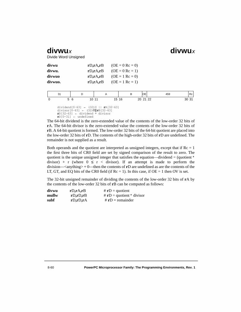
8-60 PowerPC Microprocessor Family: The Programming Environments, Rev. 1
divwux divwuxDivide Word Unsigned
divwu rD,rA,rB (OE = 0 Rc = 0)divwu. rD,rA,rB (OE = 0 Rc = 1)divwuo rD,rA,rB (OE = 1 Rc = 0)divwuo. rD,rA,rB (OE = 1 Rc = 1)
dividend[0–63] ← (32)0 || rA[32–63]divisor[0–63] ← (32)0 || rB[32–63]rD[32–63] ← dividend ÷ divisorrD[0–31] ← undefined
The 64-bit dividend is the zero-extended value of the contents of the low-order 32 bits ofrA. The 64-bit divisor is the zero-extended value the contents of the low-order 32 bits ofrB. A 64-bit quotient is formed. The low-order 32 bits of the 64-bit quotient are placed intothe low-order 32 bits of rD. The contents of the high-order 32 bits of rD are undefined. Theremainder is not supplied as a result.
Both operands and the quotient are interpreted as unsigned integers, except that if Rc = 1the first three bits of CR0 field are set by signed comparison of the result to zero. Thequotient is the unique unsigned integer that satisfies the equation—dividend = (quotient ∗divisor) + r (where 0 ≤ r < divisor). If an attempt is made to perform thedivision—<anything> ÷ 0—then the contents of rD are undefined as are the contents of theLT, GT, and EQ bits of the CR0 field (if Rc = 1). In this case, if OE = 1 then OV is set.
The 32-bit unsigned remainder of dividing the contents of the low-order 32 bits of rA bythe contents of the low-order 32 bits of rB can be computed as follows:
divwu rD,rA,rB # rD = quotientmullw rD,rD,rB # rD = quotient ∗ divisorsubf rD,rD,rA # rD = remainder
0 5 6 10 11 15 16 20 21 22 30 31
31 D A B OE 459 Rc

Chapter 8. Instruction Set 8-61
Other registers altered:
• Condition Register (CR0 field):
Affected: LT, GT, EQ, SO (if Rc = 1)
LT, GT, EQ undefined (if Rc =1 and 64-bit mode)
• XER:
Affected: SO, OV (if OE = 1)
Note: The setting of the affected bits in the XER is mode-independent, and reflects overflow of the low-order 32-bit result.
PowerPC Architecture Level Supervisor Level 32-Bit 64-Bit 64-Bit Bridge Optional Form
UISA XO

8-62 PowerPC Microprocessor Family: The Programming Environments, Rev. 1
eciwx eciwxExternal Control In Word Indexed
eciwx rD,rA,rB
The eciwx instruction and the EAR register can be very efficient when mapping specialdevices such as graphics devices that use addresses as pointers.
if rA = 0 then b ← 0else b← (rA)EA ← b + (rB)paddr ← address translation of EAsend load word request for paddr to device identified by EAR[RID]rD ← (32)0 || word from device
EA is the sum (rA|0) + (rB).
A load word request for the physical address (referred to as real address in the architecturespecification) corresponding to EA is sent to the device identified by EAR[RID], bypassingthe cache. The word returned by the device is placed in the low-order 32 bits of rD. Thecontents of the high-order 32 bits of rD are cleared.
EAR[E] must be 1. If it is not, a DSI exception is generated.
EA must be a multiple of four. If it is not, one of the following occurs:
• A system alignment exception is generated.• A DSI exception is generated (possible only if EAR[E] = 0).• The results are boundedly undefined.
The eciwx instruction is supported for EAs that reference memory segments in whichSR[T] = 1 (or STE[T] = 1) and for EAs mapped by the DBAT registers. If the EA referencesa direct-store segment (SR[T] = 1 or STE[T] = 1), either a DSI exception occurs or theresults are boundedly undefined. However, note that the direct-store facility is being phasedout of the architecture and will not likely be supported in future devices. Thus, softwareshould not depend on its effects.
If this instruction is executed when MSR[DR] = 0 (real addressing mode), the results areboundedly undefined.
This instruction is treated as a load from the addressed byte with respect to addresstranslation, memory protection, referenced and changed bit recording, and the orderingperformed by eieio.
This instruction is optional in the PowerPC architecture.
0 5 6 10 11 15 16 20 21 30 31
Reserved
31 D A B 310 0

Chapter 8. Instruction Set 8-63
Other registers altered:
• None
PowerPC Architecture Level Supervisor Level 32-Bit 64-Bit 64-Bit Bridge Optional Form
VEA √ X

8-64 PowerPC Microprocessor Family: The Programming Environments, Rev. 1
ecowx ecowxExternal Control Out Word Indexed
ecowx rS,rA,rB
The ecowx instruction and the EAR register can be very efficient when mapping specialdevices such as graphics devices that use addresses as pointers.
if rA = 0 then b ← 0else b ← (rA)EA ← b + (rB)paddr ← address translation of EAsend store word request for paddr to device identified by EAR[RID]send rS[32–63] to device
EA is the sum (rA|0) + (rB).
A store word request for the physical address corresponding to EA and the contents of thelow-order 32 bits of rS are sent to the device identified by EAR[RID], bypassing the cache.
EAR[E] must be 1, if it is not, a DSI exception is generated. EA must be a multiple of four.If it is not, one of the following occurs:
• A system alignment exception is generated.• A DSI exception is generated (possible only if EAR[E] = 0).• The results are boundedly undefined.
The ecowx instruction is supported for effective addresses that reference memory segmentsin which SR[T] = 0 (or STE[T] = 0), and for EAs mapped by the DBAT registers. If the EAreferences a direct-store segment (SR[T] = 1 or STE[T] = 1), either a DSI exception occursor the results are boundedly undefined. However, note that the direct-store facility is beingphased out of the architecture and will not likely be supported in future devices. Thus,software should not depend on its effects.
If this instruction is executed when MSR[DR] = 0 (real addressing mode), the results areboundedly undefined.
This instruction is treated as a store from the addressed byte with respect to addresstranslation, memory protection, and referenced and changed bit recording, and the orderingperformed by eieio. Note that software synchronization is required in order to ensure thatthe data access is performed in program order with respect to data accesses caused by otherstore or ecowx instructions, even though the addressed byte is assumed to be caching-inhibited and guarded.
0 5 6 10 11 15 16 20 21 30 31
Reserved
31 S A B 438 0

Chapter 8. Instruction Set 8-65
This instruction is optional in the PowerPC architecture.
Other registers altered:
• None
PowerPC Architecture Level Supervisor Level 32-Bit 64-Bit 64-Bit Bridge Optional Form
VEA √ X

8-66 PowerPC Microprocessor Family: The Programming Environments, Rev. 1
eieio eieioEnforce In-Order Execution of I/O
The eieio instruction provides an ordering function for the effects of load and storeinstructions executed by a processor. These loads and stores are divided into two sets, whichare ordered separately. The memory accesses caused by a dcbz or a dcba instruction areordered like a store. The two sets follow:
1. Loads and stores to memory that is both caching-inhibited and guarded, and stores to memory that is write-through required.
The eieio instruction controls the order in which the accesses are performed in main memory. It ensures that all applicable memory accesses caused by instructions preceding the eieio instruction have completed with respect to main memory before any applicable memory accesses caused by instructions following the eieio instruction access main memory. It acts like a barrier that flows through the memory queues and to main memory, preventing the reordering of memory accesses across the barrier. No ordering is performed for dcbz if the instruction causes the system alignment error handler to be invoked.
All accesses in this set are ordered as a single set—that is, there is not one order for loads and stores to caching-inhibited and guarded memory and another order for stores to write-through required memory.
2. Stores to memory that have all of the following attributes—caching-allowed, write-through not required, and memory-coherency required.
The eieio instruction controls the order in which the accesses are performed with respect to coherent memory. It ensures that all applicable stores caused by instructions preceding the eieio instruction have completed with respect to coherent memory before any applicable stores caused by instructions following the eieio instruction complete with respect to coherent memory.
With the exception of dcbz and dcba, eieio does not affect the order of cache operations(whether caused explicitly by execution of a cache management instruction, or implicitlyby the cache coherency mechanism). For more information, refer to Chapter 5, “CacheModel and Memory Coherency.” The eieio instruction does not affect the order of accessesin one set with respect to accesses in the other set.
The eieio instruction may complete before memory accesses caused by instructionspreceding the eieio instruction have been performed with respect to main memory orcoherent memory as appropriate.
0 5 6 10 11 15 16 20 21 30 31
Reserved
31 0 0 0 0 0 0 0 0 0 0 0 0 0 0 0 854 0

Chapter 8. Instruction Set 8-67
The eieio instruction is intended for use in managing shared data structures, in accessingmemory-mapped I/O, and in preventing load/store combining operations in main memory.For the first use, the shared data structure and the lock that protects it must be altered onlyby stores that are in the same set (1 or 2; see previous discussion). For the second use, eieiocan be thought of as placing a barrier into the stream of memory accesses issued by aprocessor, such that any given memory access appears to be on the same side of the barrierto both the processor and the I/O device.
Because the processor performs store operations in order to memory that is designated asboth caching-inhibited and guarded (refer to Section 5.1.1, “Memory Access Ordering”),the eieio instruction is needed for such memory only when loads must be ordered withrespect to stores or with respect to other loads.
Note that the eieio instruction does not connect hardware considerations to it such asmultiprocessor implementations that send an eieio address-only broadcast (useful in somedesigns). For example, if a design has an external buffer that re-orders loads and stores forbetter bus efficiency, the eieio broadcast signals to that buffer that previous loads/stores(marked caching-inhibited, guarded, or write-through required) must complete before anyfollowing loads/stores (marked caching-inhibited, guarded, or write-through required).
Other registers altered:
• None
PowerPC Architecture Level Supervisor Level 32-Bit 64-Bit 64-Bit Bridge Optional Form
VEA X

8-68 PowerPC Microprocessor Family: The Programming Environments, Rev. 1
eqvx eqvxEquivalent
eqv rA,rS,rB (Rc = 0)eqv. rA,rS,rB (Rc = 1)
rA ← (rS) ≡ (rB)The contents of rS are XORed with the contents of rB and the complemented result isplaced into rA.
Other registers altered:
• Condition Register (CR0 field):
Affected: LT, GT, EQ, SO (if Rc = 1)
PowerPC Architecture Level Supervisor Level 32-Bit 64-Bit 64-Bit Bridge Optional Form
UISA X
0 5 6 10 11 15 16 21 22 30 31
31 S A B 284 Rc
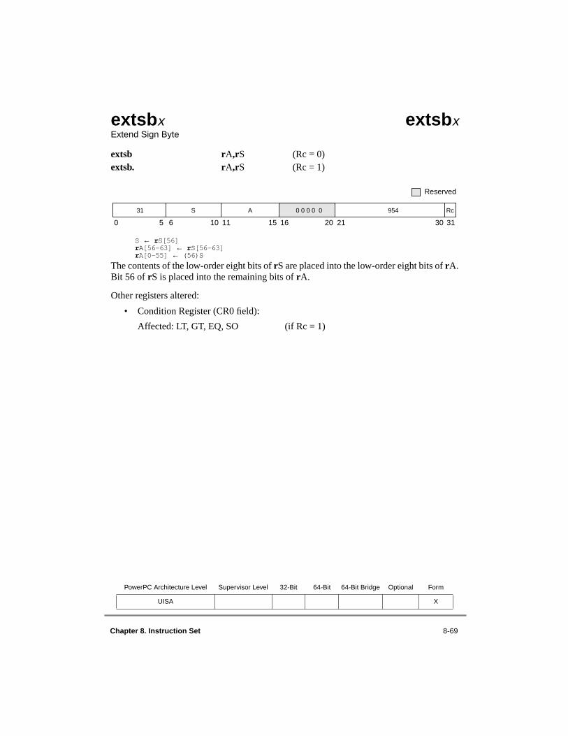
Chapter 8. Instruction Set 8-69
extsbx extsbxExtend Sign Byte
extsb rA,rS (Rc = 0)extsb. rA,rS (Rc = 1)
S ← rS[56]rA[56–63] ← rS[56–63]rA[0–55] ← (56)S
The contents of the low-order eight bits of rS are placed into the low-order eight bits of rA.Bit 56 of rS is placed into the remaining bits of rA.
Other registers altered:
• Condition Register (CR0 field):
Affected: LT, GT, EQ, SO (if Rc = 1)
PowerPC Architecture Level Supervisor Level 32-Bit 64-Bit 64-Bit Bridge Optional Form
UISA X
0 5 6 10 11 15 16 20 21 30 31
Reserved
31 S A 0 0 0 0 0 954 Rc
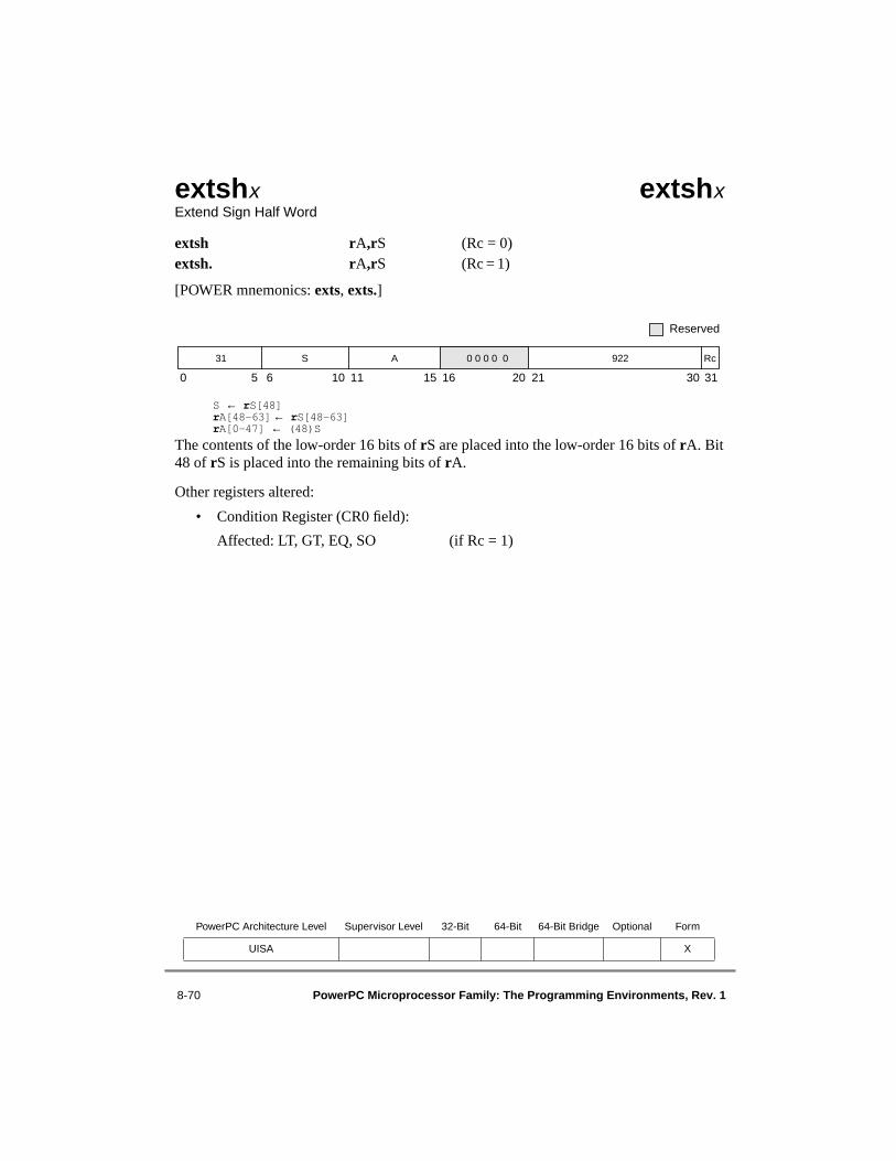
8-70 PowerPC Microprocessor Family: The Programming Environments, Rev. 1
extshx extshxExtend Sign Half Word
extsh rA,rS (Rc = 0)extsh. rA,rS (Rc = 1)
[POWER mnemonics: exts, exts.]
S ← rS[48]rA[48–63] ← rS[48–63]rA[0–47] ← (48)S
The contents of the low-order 16 bits of rS are placed into the low-order 16 bits of rA. Bit48 of rS is placed into the remaining bits of rA.
Other registers altered:
• Condition Register (CR0 field):
Affected: LT, GT, EQ, SO (if Rc = 1)
PowerPC Architecture Level Supervisor Level 32-Bit 64-Bit 64-Bit Bridge Optional Form
UISA X
0 5 6 10 11 15 16 20 21 30 31
Reserved
31 S A 0 0 0 0 0 922 Rc

Chapter 8. Instruction Set 8-71
extswx 64-Bit Implementations Only extswxExtend Sign Word
extsw rA,rS (Rc = 0)extsw. rA,rS (Rc = 1)
S ← rS[32]rA[32–63] ← rS[32–63]rA[0–31] ← (32)S
The contents of the low-order 32 bits of rS are placed into the low-order 32 bits of rA. Bit32 of rS is placed into the high-order 32 bits of rA.
This instruction is defined only for 64-bit implementations. Using it on a 32-bitimplementation will cause the system illegal instruction error handler to be invoked.
Other registers altered:
• Condition Register (CR0 field):
Affected: LT, GT, EQ, SO (if Rc = 1)
PowerPC Architecture Level Supervisor Level 32-Bit 64-Bit 64-Bit Bridge Optional Form
UISA √ X
0 5 6 10 11 15 16 20 21 30 31
Reserved
31 S A 0 0 0 0 0 986 Rc

8-72 PowerPC Microprocessor Family: The Programming Environments, Rev. 1
fabsx fabsxFloating Absolute Value
fabs frD,frB (Rc = 0)fabs. frD,frB (Rc = 1)
The contents of frB with bit 0 cleared are placed into frD.
Note that the fabs instruction treats NaNs just like any other kind of value. That is, the signbit of a NaN may be altered by fabs. This instruction does not alter the FPSCR.
Other registers altered:
• Condition Register (CR1 field):
Affected: FX, FEX, VX, OX (if Rc = 1)
PowerPC Architecture Level Supervisor Level 32-Bit 64-Bit 64-Bit Bridge Optional Form
UISA X
B 264 Rc
0 5 6 10 11 15 16 20 21 30 31
Reserved
63 D 0 0 0 0 0

Chapter 8. Instruction Set 8-73
faddx faddxFloating Add (Double-Precision)
fadd frD,frA,frB (Rc = 0)fadd. frD,frA,frB (Rc = 1)
[POWER mnemonics: fa, fa.]
The floating-point operand in frA is added to the floating-point operand in frB. If the most-significant bit of the resultant significand is not a one, the result is normalized. The resultis rounded to double-precision under control of the floating-point rounding control field RNof the FPSCR and placed into frD.
Floating-point addition is based on exponent comparison and addition of the twosignificands. The exponents of the two operands are compared, and the significandaccompanying the smaller exponent is shifted right, with its exponent increased by one foreach bit shifted, until the two exponents are equal. The two significands are then added orsubtracted as appropriate, depending on the signs of the operands. All 53 bits in thesignificand as well as all three guard bits (G, R, and X) enter into the computation.
If a carry occurs, the sum's significand is shifted right one bit position and the exponent isincreased by one. FPSCR[FPRF] is set to the class and sign of the result, except for invalidoperation exceptions when FPSCR[VE] = 1.
Other registers altered:
• Condition Register (CR1 field):
Affected: FX, FEX, VX, OX (if Rc = 1)
• Floating-Point Status and Control Register:
Affected: FPRF, FR, FI, FX, OX, UX, XX,VXSNAN, VXISI
PowerPC Architecture Level Supervisor Level 32-Bit 64-Bit 64-Bit Bridge Optional Form
UISA A
0 5 6 10 11 15 16 20 21 25 26 30 31
Reserved
63 D A B 0 0 0 0 0 21 Rc

8-74 PowerPC Microprocessor Family: The Programming Environments, Rev. 1
faddsx faddsxFloating Add Single
fadds frD,frA,frB (Rc = 0)fadds. frD,frA,frB (Rc = 1)
The floating-point operand in frA is added to the floating-point operand in frB. If the most-significant bit of the resultant significand is not a one, the result is normalized. The resultis rounded to the single-precision under control of the floating-point rounding control fieldRN of the FPSCR and placed into frD.
Floating-point addition is based on exponent comparison and addition of the twosignificands. The exponents of the two operands are compared, and the significandaccompanying the smaller exponent is shifted right, with its exponent increased by one foreach bit shifted, until the two exponents are equal. The two significands are then added orsubtracted as appropriate, depending on the signs of the operands. All 53 bits in thesignificand as well as all three guard bits (G, R, and X) enter into the computation.
If a carry occurs, the sum's significand is shifted right one bit position and the exponent isincreased by one. FPSCR[FPRF] is set to the class and sign of the result, except for invalidoperation exceptions when FPSCR[VE] = 1.
Other registers altered:
• Condition Register (CR1 field):
Affected: FX, FEX, VX, OX (if Rc = 1)
• Floating-Point Status and Control Register:
Affected: FPRF, FR, FI, FX, OX, UX, XX,VXSNAN, VXISI
PowerPC Architecture Level Supervisor Level 32-Bit 64-Bit 64-Bit Bridge Optional Form
UISA A
0 5 6 10 11 15 16 20 21 25 26 30 31
Reserved
59 D A B 0 0 0 0 0 21 Rc
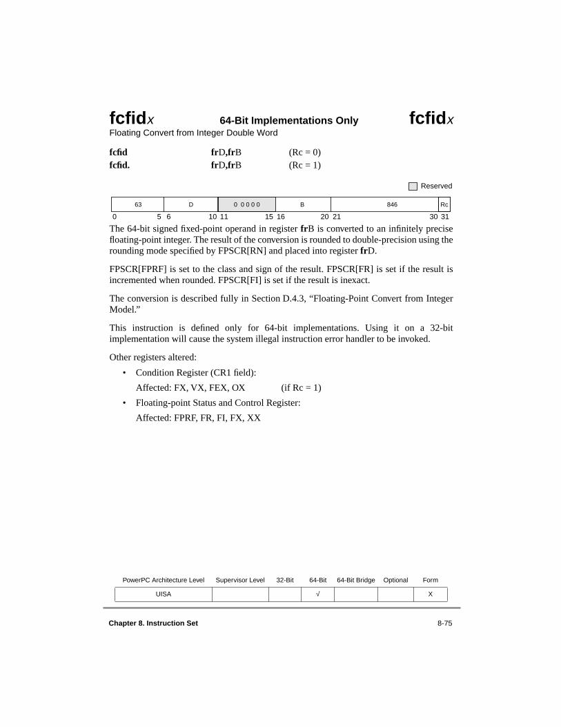
Chapter 8. Instruction Set 8-75
fcfidx 64-Bit Implementations Only fcfidxFloating Convert from Integer Double Word
fcfid frD,frB (Rc = 0)fcfid. frD,frB (Rc = 1)
The 64-bit signed fixed-point operand in register frB is converted to an infinitely precisefloating-point integer. The result of the conversion is rounded to double-precision using therounding mode specified by FPSCR[RN] and placed into register frD.
FPSCR[FPRF] is set to the class and sign of the result. FPSCR[FR] is set if the result isincremented when rounded. FPSCR[FI] is set if the result is inexact.
The conversion is described fully in Section D.4.3, “Floating-Point Convert from IntegerModel.”
This instruction is defined only for 64-bit implementations. Using it on a 32-bitimplementation will cause the system illegal instruction error handler to be invoked.
Other registers altered:
• Condition Register (CR1 field):
Affected: FX, VX, FEX, OX (if Rc = 1)
• Floating-point Status and Control Register:
Affected: FPRF, FR, FI, FX, XX
PowerPC Architecture Level Supervisor Level 32-Bit 64-Bit 64-Bit Bridge Optional Form
UISA √ X
0 5 6 10 11 15 16 20 21 30 31
Reserved
63 D 0 0 0 0 0 B 846 Rc

8-76 PowerPC Microprocessor Family: The Programming Environments, Rev. 1
fcmpo fcmpo Floating Compare Ordered
fcmpo crfD,frA,frB
if (frA) is a NaN or(frB) is a NaN then c ← 0b0001
else if (frA)< (frB) then c ← 0b1000else if (frA)> (frB) then c ← 0b0100else c ← 0b0010
FPCC ← cCR[4 ∗ crfD–4 ∗ crfD + 3] ← c
if (frA) is an SNaN or(frB) is an SNaN then
VXSNAN ← 1if VE = 0 then VXVC ← 1
else if (frA) is a QNaN or(frB) is a QNaN then VXVC ← 1
The floating-point operand in frA is compared to the floating-point operand in frB. Theresult of the compare is placed into CR field crfD and the FPCC.
If one of the operands is a NaN, either quiet or signaling, then CR field crfD and the FPCCare set to reflect unordered. If one of the operands is a signaling NaN, then VXSNAN is set,and if invalid operation is disabled (VE = 0) then VXVC is set. Otherwise, if one of theoperands is a QNaN, then VXVC is set.
Other registers altered:
• Condition Register (CR field specified by operand crfD):
Affected: LT, GT, EQ, UN
• Floating-Point Status and Control Register:
Affected: FPCC, FX, VXSNAN, VXVC
PowerPC Architecture Level Supervisor Level 32-Bit 64-Bit 64-Bit Bridge Optional Form
UISA X
0 5 6 8 9 10 11 15 16 20 21 30 31
Reserved
B 32 063 crfD 0 0 A

Chapter 8. Instruction Set 8-77
fcmpu fcmpu Floating Compare Unordered
fcmpu crfD,frA,frB
if (frA) is a NaN or(frB) is a NaN then c ← 0b0001
else if (frA) < (frB) then c ← 0b1000else if (frA) > (frB) then c ← 0b0100else c ← 0b0010
FPCC ← cCR[4 ∗ crfD–4 ∗ crfD + 3] ← c
if (frA) is an SNaN or(frB) is an SNaN then
VXSNAN ← 1
The floating-point operand in register frA is compared to the floating-point operand inregister frB. The result of the compare is placed into CR field crfD and the FPCC.
If one of the operands is a NaN, either quiet or signaling, then CR field crfD and the FPCCare set to reflect unordered. If one of the operands is a signaling NaN, then VXSNAN is set.
Other registers altered:
• Condition Register (CR field specified by operand crfD):
Affected: LT, GT, EQ, UN
• Floating-Point Status and Control Register:
Affected: FPCC, FX, VXSNAN
PowerPC Architecture Level Supervisor Level 32-Bit 64-Bit 64-Bit Bridge Optional Form
UISA X
0 5 6 8 9 10 11 15 16 20 21 30 31
Reserved
B 0 0 0 0 0 0 0 0 0 0 063 crfD 0 0 A
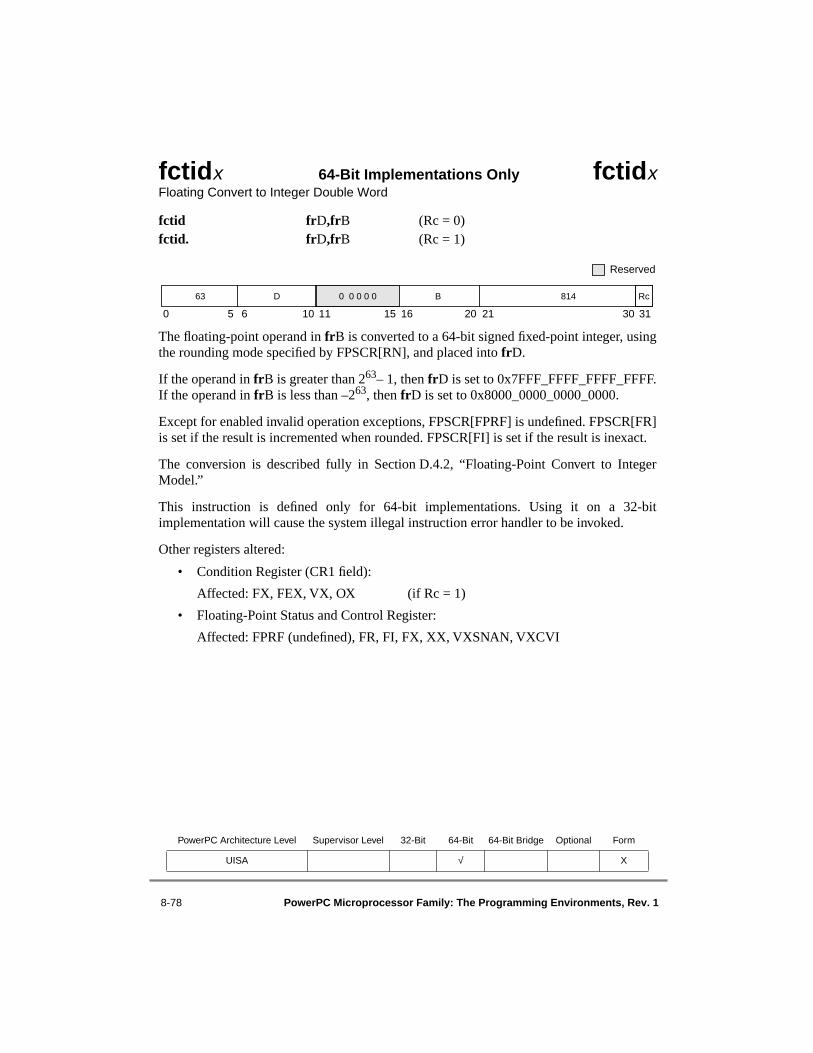
8-78 PowerPC Microprocessor Family: The Programming Environments, Rev. 1
fctidx 64-Bit Implementations Only fctidxFloating Convert to Integer Double Word
fctid frD,frB (Rc = 0)fctid. frD,frB (Rc = 1)
The floating-point operand in frB is converted to a 64-bit signed fixed-point integer, usingthe rounding mode specified by FPSCR[RN], and placed into frD.
If the operand in frB is greater than 263– 1, then frD is set to 0x7FFF_FFFF_FFFF_FFFF.If the operand in frB is less than –263, then frD is set to 0x8000_0000_0000_0000.
Except for enabled invalid operation exceptions, FPSCR[FPRF] is undefined. FPSCR[FR]is set if the result is incremented when rounded. FPSCR[FI] is set if the result is inexact.
The conversion is described fully in Section D.4.2, “Floating-Point Convert to IntegerModel.”
This instruction is defined only for 64-bit implementations. Using it on a 32-bitimplementation will cause the system illegal instruction error handler to be invoked.
Other registers altered:
• Condition Register (CR1 field):
Affected: FX, FEX, VX, OX (if Rc = 1)
• Floating-Point Status and Control Register:
Affected: FPRF (undefined), FR, FI, FX, XX, VXSNAN, VXCVI
PowerPC Architecture Level Supervisor Level 32-Bit 64-Bit 64-Bit Bridge Optional Form
UISA √ X
0 5 6 10 11 15 16 20 21 30 31
Reserved
63 D 0 0 0 0 0 B 814 Rc

Chapter 8. Instruction Set 8-79
fctidzx 64-Bit Implementations Only fctidzxFloating Convert to Integer Double Word with Round toward Zero
fctidz frD,frB (Rc = 0)fctidz. frD,frB (Rc = 1)
The floating-point operand in frB is converted to a 64-bit signed fixed-point integer, usingthe rounding mode round toward zero, and placed into frD.
If the operand in frB is greater than 263 – 1, then frD is set to 0x7FFF_FFFF_FFFF_FFFF.If the operand in frB is less than –263, then frD is set to 0x8000_0000_0000_0000.
Except for enabled invalid operation exceptions, FPSCR[FPRF] is undefined. FPSCR[FR]is set if the result is incremented when rounded. FPSCR[FI] is set if the result is inexact.
The conversion is described fully in Section D.4.2, “Floating-Point Convert to IntegerModel.”
This instruction is defined only for 64-bit implementations. Using it on a 32-bitimplementation will cause the system illegal instruction error handler to be invoked.
Other registers altered:
• Condition Register (CR1 field):
Affected: FX, FEX, VX, OX (if Rc = 1)
• Floating-Point Status and Control Register:
Affected: FPRF (undefined), FR, FI, FX, XX, VXSNAN, VXCVI
PowerPC Architecture Level Supervisor Level 32-Bit 64-Bit 64-Bit Bridge Optional Form
UISA √ X
0 5 6 10 11 15 16 20 21 30 31
Reserved
63 D 0 0 0 0 0 B 815 Rc

8-80 PowerPC Microprocessor Family: The Programming Environments, Rev. 1
fctiwx fctiwxFloating Convert to Integer Word
fctiw frD,frB (Rc = 0)fctiw. frD,frB (Rc = 1)
The floating-point operand in register frB is converted to a 32-bit signed integer, using therounding mode specified by FPSCR[RN], and placed in bits 32–63 of frD. Bits 0–31 of frDare undefined.
If the operand in frB are greater than 231 – 1, bits 32–63 of frD are set to 0x7FFF_FFFF.
If the operand in frB are less than –231, bits 32–63 of frD are set to 0x8000_0000.
The conversion is described fully in Section D.4.2, “Floating-Point Convert to IntegerModel.”
Except for trap-enabled invalid operation exceptions, FPSCR[FPRF] is undefined.FPSCR[FR] is set if the result is incremented when rounded. FPSCR[FI] is set if the resultis inexact.
Other registers altered:
• Condition Register (CR1 field):
Affected: FX, FEX, VX, OX (if Rc = 1)
• Floating-Point Status and Control Register:
Affected: FPRF (undefined), FR, FI, FX, XX, VXSNAN, VXCVI
PowerPC Architecture Level Supervisor Level 32-Bit 64-Bit 64-Bit Bridge Optional Form
UISA X
0 5 6 10 11 15 16 20 21 30 31
Reserved
B 14 Rc63 D 0 0 0 0 0
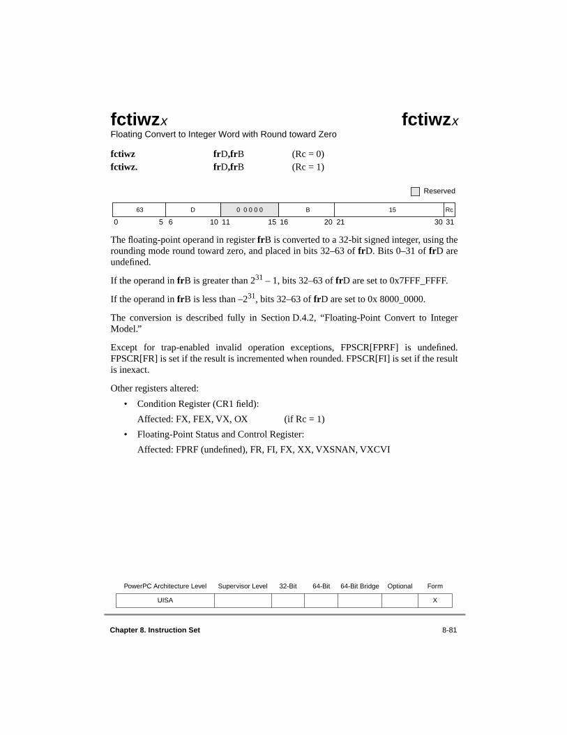
Chapter 8. Instruction Set 8-81
fctiwzx fctiwzxFloating Convert to Integer Word with Round toward Zero
fctiwz frD,frB (Rc = 0)fctiwz. frD,frB (Rc = 1)
The floating-point operand in register frB is converted to a 32-bit signed integer, using therounding mode round toward zero, and placed in bits 32–63 of frD. Bits 0–31 of frD areundefined.
If the operand in frB is greater than 231 – 1, bits 32–63 of frD are set to 0x7FFF_FFFF.
If the operand in frB is less than –231, bits 32–63 of frD are set to 0x 8000_0000.
The conversion is described fully in Section D.4.2, “Floating-Point Convert to IntegerModel.”
Except for trap-enabled invalid operation exceptions, FPSCR[FPRF] is undefined.FPSCR[FR] is set if the result is incremented when rounded. FPSCR[FI] is set if the resultis inexact.
Other registers altered:
• Condition Register (CR1 field):
Affected: FX, FEX, VX, OX (if Rc = 1)
• Floating-Point Status and Control Register:
Affected: FPRF (undefined), FR, FI, FX, XX, VXSNAN, VXCVI
PowerPC Architecture Level Supervisor Level 32-Bit 64-Bit 64-Bit Bridge Optional Form
UISA X
0 5 6 10 11 15 16 20 21 30 31
Reserved
B 15 Rc63 D 0 0 0 0 0

8-82 PowerPC Microprocessor Family: The Programming Environments, Rev. 1
fdivx fdivxFloating Divide (Double-Precision)
fdiv frD,frA,frB (Rc = 0)fdiv. frD,frA,frB (Rc = 1)
[POWER mnemonics: fd, fd.]
The floating-point operand in register frA is divided by the floating-point operand inregister frB. The remainder is not supplied as a result.
If the most-significant bit of the resultant significand is not a one, the result is normalized.The result is rounded to double-precision under control of the floating-point roundingcontrol field RN of the FPSCR and placed into frD.
Floating-point division is based on exponent subtraction and division of the significands.
FPSCR[FPRF] is set to the class and sign of the result, except for invalid operationexceptions when FPSCR[VE] = 1 and zero divide exceptions when FPSCR[ZE] = 1.
Other registers altered:
• Condition Register (CR1 field):
Affected: FX, FEX, VX, OX (if Rc = 1)
• Floating-Point Status and Control Register:
Affected: FPRF, FR, FI, FX, OX, UX, ZX, XX, VXSNAN, VXIDI, VXZDZ
PowerPC Architecture Level Supervisor Level 32-Bit 64-Bit 64-Bit Bridge Optional Form
UISA A
0 5 6 10 11 15 16 20 21 25 26 30 31
Reserved
B 0 0 0 0 0 18 Rc63 D A
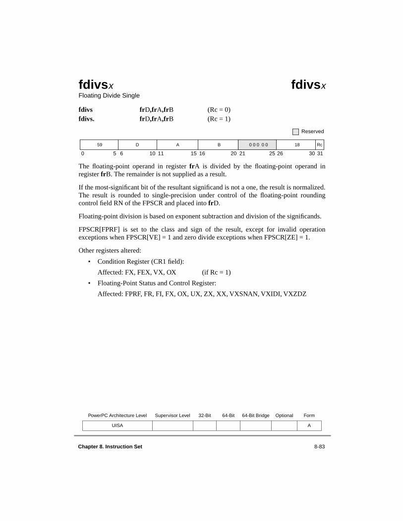
Chapter 8. Instruction Set 8-83
fdivsx fdivsxFloating Divide Single
fdivs frD,frA,frB (Rc = 0)fdivs. frD,frA,frB (Rc = 1)
The floating-point operand in register frA is divided by the floating-point operand inregister frB. The remainder is not supplied as a result.
If the most-significant bit of the resultant significand is not a one, the result is normalized.The result is rounded to single-precision under control of the floating-point roundingcontrol field RN of the FPSCR and placed into frD.
Floating-point division is based on exponent subtraction and division of the significands.
FPSCR[FPRF] is set to the class and sign of the result, except for invalid operationexceptions when FPSCR[VE] = 1 and zero divide exceptions when FPSCR[ZE] = 1.
Other registers altered:
• Condition Register (CR1 field):
Affected: FX, FEX, VX, OX (if Rc = 1)
• Floating-Point Status and Control Register:
Affected: FPRF, FR, FI, FX, OX, UX, ZX, XX, VXSNAN, VXIDI, VXZDZ
PowerPC Architecture Level Supervisor Level 32-Bit 64-Bit 64-Bit Bridge Optional Form
UISA A
0 5 6 10 11 15 16 20 21 25 26 30 31
Reserved
B 0 0 0 0 0 18 Rc59 D A
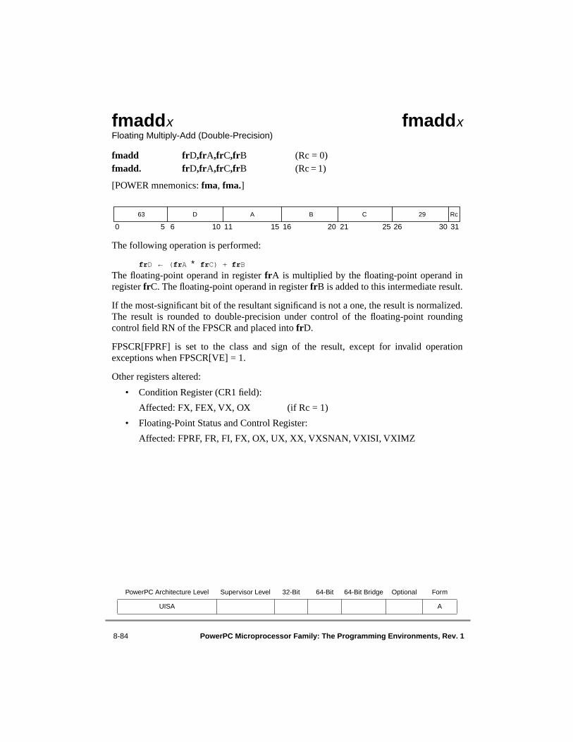
8-84 PowerPC Microprocessor Family: The Programming Environments, Rev. 1
fmaddx fmaddxFloating Multiply-Add (Double-Precision)
fmadd frD,frA,frC,frB (Rc = 0)fmadd. frD,frA,frC,frB (Rc = 1)
[POWER mnemonics: fma, fma.]
The following operation is performed:
frD ← (frA ∗ frC) + frBThe floating-point operand in register frA is multiplied by the floating-point operand inregister frC. The floating-point operand in register frB is added to this intermediate result.
If the most-significant bit of the resultant significand is not a one, the result is normalized.The result is rounded to double-precision under control of the floating-point roundingcontrol field RN of the FPSCR and placed into frD.
FPSCR[FPRF] is set to the class and sign of the result, except for invalid operationexceptions when FPSCR[VE] = 1.
Other registers altered:
• Condition Register (CR1 field):
Affected: FX, FEX, VX, OX (if Rc = 1)
• Floating-Point Status and Control Register:
Affected: FPRF, FR, FI, FX, OX, UX, XX, VXSNAN, VXISI, VXIMZ
PowerPC Architecture Level Supervisor Level 32-Bit 64-Bit 64-Bit Bridge Optional Form
UISA A
0 5 6 10 11 15 16 20 21 25 26 30 31
B C 29 Rc63 D A

Chapter 8. Instruction Set 8-85
fmaddsx fmaddsxFloating Multiply-Add Single
fmadds frD,frA,frC,frB (Rc = 0) fmadds. frD,frA,frC,frB (Rc = 1)
The following operation is performed:
frD ← (frA ∗ frC) + frBThe floating-point operand in register frA is multiplied by the floating-point operand inregister frC. The floating-point operand in register frB is added to this intermediate result.
If the most-significant bit of the resultant significand is not a one, the result is normalized.The result is rounded to single-precision under control of the floating-point roundingcontrol field RN of the FPSCR and placed into frD.
FPSCR[FPRF] is set to the class and sign of the result, except for invalid operationexceptions when FPSCR[VE] = 1.
Other registers altered:
• Condition Register (CR1 field):
Affected: FX, FEX, VX, OX (if Rc = 1)
• Floating-Point Status and Control Register:
Affected: FPRF, FR, FI, FX, OX, UX, XX, VXSNAN, VXISI, VXIMZ
PowerPC Architecture Level Supervisor Level 32-Bit 64-Bit 64-Bit Bridge Optional Form
UISA A
0 5 6 10 11 15 16 20 21 25 26 30 31
B C 29 Rc59 D A

8-86 PowerPC Microprocessor Family: The Programming Environments, Rev. 1
fmrx fmrxFloating Move Register
fmr frD,frB (Rc = 0)fmr. frD,frB (Rc = 1)
The contents of register frB are placed into frD.
Other registers altered:
• Condition Register (CR1 field):
Affected: FX, FEX, VX, OX (if Rc = 1)
PowerPC Architecture Level Supervisor Level 32-Bit 64-Bit 64-Bit Bridge Optional Form
UISA X
0 5 6 10 11 15 16 20 21 30 31
Reserved
B 72 Rc63 D 0 0 0 0 0

Chapter 8. Instruction Set 8-87
fmsubx fmsubxFloating Multiply-Subtract (Double-Precision)
fmsub frD,frA,frC,frB (Rc = 0)fmsub. frD,frA,frC,frB (Rc = 1)
[POWER mnemonics: fms, fms.]
The following operation is performed:
frD ← [frA ∗ frC] – frBThe floating-point operand in register frA is multiplied by the floating-point operand inregister frC. The floating-point operand in register frB is subtracted from this intermediateresult.
If the most-significant bit of the resultant significand is not a one, the result is normalized.The result is rounded to double-precision under control of the floating-point roundingcontrol field RN of the FPSCR and placed into frD.
FPSCR[FPRF] is set to the class and sign of the result, except for invalid operationexceptions when FPSCR[VE] = 1.
Other registers altered:
• Condition Register (CR1 field):
Affected: FX, FEX, VX, OX (if Rc = 1)
• Floating-Point Status and Control Register:
Affected: FPRF, FR, FI, FX, OX, UX, XX, VXSNAN, VXISI, VXIMZ
PowerPC Architecture Level Supervisor Level 32-Bit 64-Bit 64-Bit Bridge Optional Form
UISA A
0 5 6 10 11 15 16 20 21 25 26 30 31
B C 28 Rc63 D A
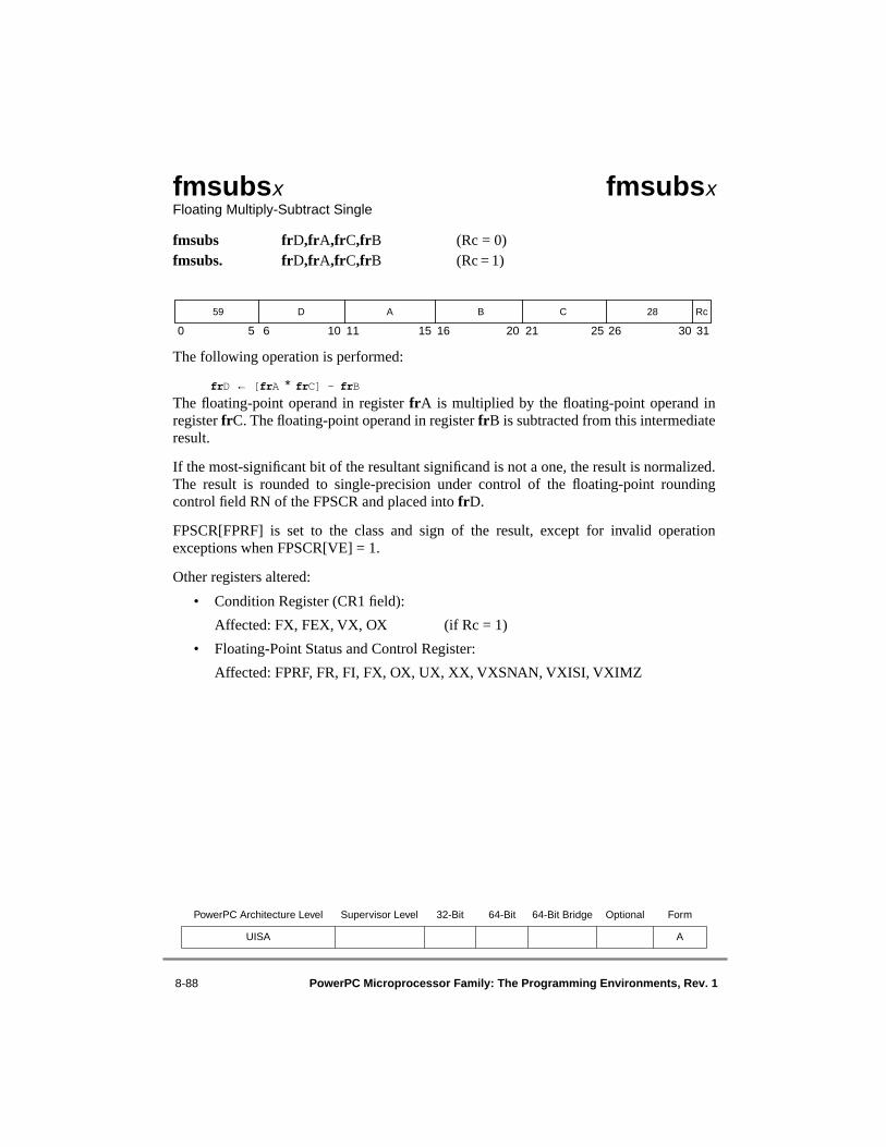
8-88 PowerPC Microprocessor Family: The Programming Environments, Rev. 1
fmsubsx fmsubsxFloating Multiply-Subtract Single
fmsubs frD,frA,frC,frB (Rc = 0)fmsubs. frD,frA,frC,frB (Rc = 1)
The following operation is performed:
frD ← [frA ∗ frC] – frBThe floating-point operand in register frA is multiplied by the floating-point operand inregister frC. The floating-point operand in register frB is subtracted from this intermediateresult.
If the most-significant bit of the resultant significand is not a one, the result is normalized.The result is rounded to single-precision under control of the floating-point roundingcontrol field RN of the FPSCR and placed into frD.
FPSCR[FPRF] is set to the class and sign of the result, except for invalid operationexceptions when FPSCR[VE] = 1.
Other registers altered:
• Condition Register (CR1 field):
Affected: FX, FEX, VX, OX (if Rc = 1)
• Floating-Point Status and Control Register:
Affected: FPRF, FR, FI, FX, OX, UX, XX, VXSNAN, VXISI, VXIMZ
PowerPC Architecture Level Supervisor Level 32-Bit 64-Bit 64-Bit Bridge Optional Form
UISA A
0 5 6 10 11 15 16 20 21 25 26 30 31
B C 28 Rc59 D A
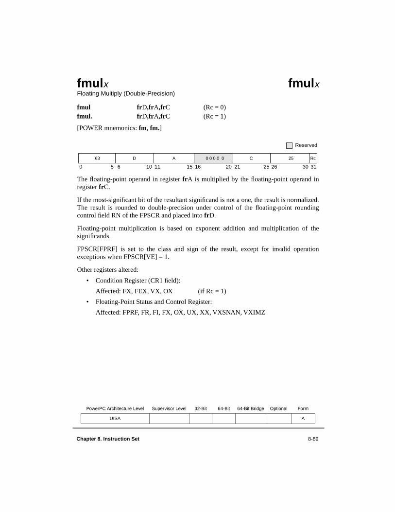
Chapter 8. Instruction Set 8-89
fmulx fmulxFloating Multiply (Double-Precision)
fmul frD,frA,frC (Rc = 0)fmul. frD,frA,frC (Rc = 1)
[POWER mnemonics: fm, fm.]
The floating-point operand in register frA is multiplied by the floating-point operand inregister frC.
If the most-significant bit of the resultant significand is not a one, the result is normalized.The result is rounded to double-precision under control of the floating-point roundingcontrol field RN of the FPSCR and placed into frD.
Floating-point multiplication is based on exponent addition and multiplication of thesignificands.
FPSCR[FPRF] is set to the class and sign of the result, except for invalid operationexceptions when FPSCR[VE] = 1.
Other registers altered:
• Condition Register (CR1 field):
Affected: FX, FEX, VX, OX (if Rc = 1)
• Floating-Point Status and Control Register:
Affected: FPRF, FR, FI, FX, OX, UX, XX, VXSNAN, VXIMZ
PowerPC Architecture Level Supervisor Level 32-Bit 64-Bit 64-Bit Bridge Optional Form
UISA A
0 5 6 10 11 15 16 20 21 25 26 30 31
Reserved
0 0 0 0 0 C 25 Rc63 D A

8-90 PowerPC Microprocessor Family: The Programming Environments, Rev. 1
fmulsx fmulsxFloating Multiply Single
fmuls frD,frA,frC (Rc = 0)fmuls. frD,frA,frC (Rc = 1)
The floating-point operand in register frA is multiplied by the floating-point operand inregister frC.
If the most-significant bit of the resultant significand is not a one, the result is normalized.The result is rounded to single-precision under control of the floating-point roundingcontrol field RN of the FPSCR and placed into frD.
Floating-point multiplication is based on exponent addition and multiplication of thesignificands.
FPSCR[FPRF] is set to the class and sign of the result, except for invalid operationexceptions when FPSCR[VE] = 1.
Other registers altered:
• Condition Register (CR1 field):
Affected: FX, FEX, VX, OX (if Rc = 1)
• Floating-Point Status and Control Register:
Affected: FPRF, FR, FI, FX, OX, UX, XX, VXSNAN, VXIMZ
PowerPC Architecture Level Supervisor Level 32-Bit 64-Bit 64-Bit Bridge Optional Form
UISA A
0 5 6 10 11 15 16 20 21 25 26 30 31
Reserved
0 0 0 0 0 C 25 Rc59 D A

Chapter 8. Instruction Set 8-91
fnabsx fnabsxFloating Negative Absolute Value
fnabs frD,frB (Rc = 0)fnabs. frD,frB (Rc = 1)
The contents of register frB with bit 0 set are placed into frD.
Note that the fnabs instruction treats NaNs just like any other kind of value. That is, thesign bit of a NaN may be altered by fnabs. This instruction does not alter the FPSCR.
Other registers altered:
• Condition Register (CR1 field):
Affected: FX, FEX, VX, OX (if Rc = 1)
PowerPC Architecture Level Supervisor Level 32-Bit 64-Bit 64-Bit Bridge Optional Form
UISA X
0 5 6 10 11 15 16 20 21 25 26 30 31
Reserved
B 136 Rc63 D 0 0 0 0 0

8-92 PowerPC Microprocessor Family: The Programming Environments, Rev. 1
fnegx fnegxFloating Negate
fneg frD,frB (Rc = 0)fneg. frD,frB (Rc = 1)
The contents of register frB with bit 0 inverted are placed into frD.
Note that the fneg instruction treats NaNs just like any other kind of value. That is, the signbit of a NaN may be altered by fneg. This instruction does not alter the FPSCR.
Other registers altered:
• Condition Register (CR1 field):
Affected: FX, FEX, VX, OX (if Rc = 1)
PowerPC Architecture Level Supervisor Level 32-Bit 64-Bit 64-Bit Bridge Optional Form
UISA X
0 5 6 10 11 15 16 20 21 30 31
Reserved
B 40 Rc63 D 0 0 0 0 0

Chapter 8. Instruction Set 8-93
fnmaddx fnmaddx Floating Negative Multiply-Add (Double-Precision)
fnmadd frD,frA,frC,frB (Rc = 0)fnmadd. frD,frA,frC,frB (Rc = 1)
[POWER mnemonics: fnma, fnma.]
The following operation is performed:
frD ← – ([frA ∗ frC] + frB)The floating-point operand in register frA is multiplied by the floating-point operand inregister frC. The floating-point operand in register frB is added to this intermediate result.If the most-significant bit of the resultant significand is not a one, the result is normalized.The result is rounded to double-precision under control of the floating-point roundingcontrol field RN of the FPSCR, then negated and placed into frD.
This instruction produces the same result as would be obtained by using the FloatingMultiply-Add (fmaddx) instruction and then negating the result, with the followingexceptions:
• QNaNs propagate with no effect on their sign bit.
• QNaNs that are generated as the result of a disabled invalid operation exception have a sign bit of zero.
• SNaNs that are converted to QNaNs as the result of a disabled invalid operation exception retain the sign bit of the SNaN.
FPSCR[FPRF] is set to the class and sign of the result, except for invalid operationexceptions when FPSCR[VE] = 1.
Other registers altered:
• Condition Register (CR1 field):
Affected: FX, FEX, VX, OX (if Rc = 1)
• Floating-Point Status and Control Register:
Affected: FPRF, FR, FI, FX, OX, UX, XX, VXSNAN, VXISI, VXIMZ
PowerPC Architecture Level Supervisor Level 32-Bit 64-Bit 64-Bit Bridge Optional Form
UISA A
0 5 6 10 11 15 16 20 21 25 26 30 31
B C 31 Rc63 D A

8-94 PowerPC Microprocessor Family: The Programming Environments, Rev. 1
fnmaddsx fnmaddsx Floating Negative Multiply-Add Single
fnmadds frD,frA,frC,frB (Rc = 0)fnmadds. frD,frA,frC,frB (Rc = 1)
The following operation is performed:
frD ← – ([frA ∗ frC] + frB)The floating-point operand in register frA is multiplied by the floating-point operand inregister frC. The floating-point operand in register frB is added to this intermediate result.If the most-significant bit of the resultant significand is not a one, the result is normalized.The result is rounded to single-precision under control of the floating-point roundingcontrol field RN of the FPSCR, then negated and placed into frD.
This instruction produces the same result as would be obtained by using the FloatingMultiply-Add Single (fmaddsx) instruction and then negating the result, with the followingexceptions:
• QNaNs propagate with no effect on their sign bit.
• QNaNs that are generated as the result of a disabled invalid operation exception have a sign bit of zero.
• SNaNs that are converted to QNaNs as the result of a disabled invalid operation exception retain the sign bit of the SNaN.
FPSCR[FPRF] is set to the class and sign of the result, except for invalid operationexceptions when FPSCR[VE] = 1.
Other registers altered:
• Condition Register (CR1 field):
Affected: FX, FEX, VX, OX (if Rc = 1)
• Floating-Point Status and Control Register:
Affected: FPRF, FR, FI, FX, OX, UX, XX, VXSNAN, VXISI, VXIMZ
PowerPC Architecture Level Supervisor Level 32-Bit 64-Bit 64-Bit Bridge Optional Form
UISA A
0 5 6 10 11 15 16 20 21 25 26 30 31
B C 31 Rc59 D A
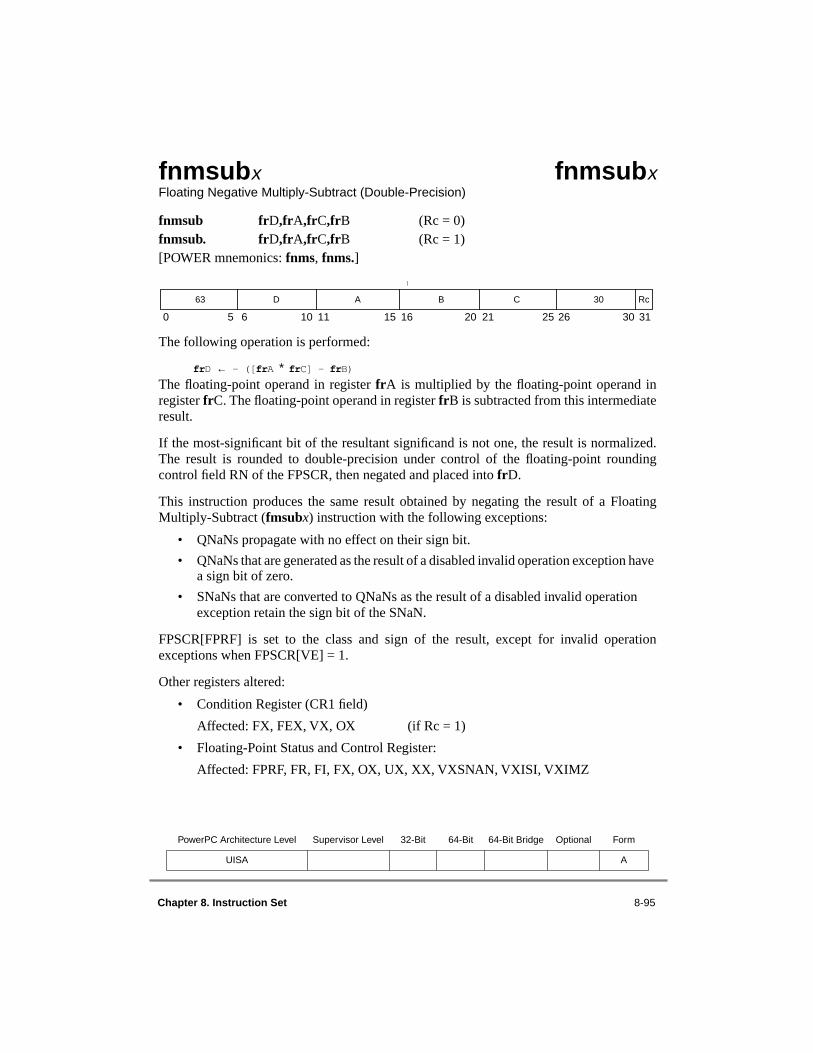
Chapter 8. Instruction Set 8-95
fnmsubx fnmsubxFloating Negative Multiply-Subtract (Double-Precision)
fnmsub frD,frA,frC,frB (Rc = 0)fnmsub. frD,frA,frC,frB (Rc = 1)[POWER mnemonics: fnms, fnms.]
]
The following operation is performed:
frD ← – ([frA ∗ frC] – frB)The floating-point operand in register frA is multiplied by the floating-point operand inregister frC. The floating-point operand in register frB is subtracted from this intermediateresult.
If the most-significant bit of the resultant significand is not one, the result is normalized.The result is rounded to double-precision under control of the floating-point roundingcontrol field RN of the FPSCR, then negated and placed into frD.
This instruction produces the same result obtained by negating the result of a FloatingMultiply-Subtract (fmsubx) instruction with the following exceptions:
• QNaNs propagate with no effect on their sign bit.
• QNaNs that are generated as the result of a disabled invalid operation exception have a sign bit of zero.
• SNaNs that are converted to QNaNs as the result of a disabled invalid operation exception retain the sign bit of the SNaN.
FPSCR[FPRF] is set to the class and sign of the result, except for invalid operationexceptions when FPSCR[VE] = 1.
Other registers altered:
• Condition Register (CR1 field)
Affected: FX, FEX, VX, OX (if Rc = 1)
• Floating-Point Status and Control Register:
Affected: FPRF, FR, FI, FX, OX, UX, XX, VXSNAN, VXISI, VXIMZ
PowerPC Architecture Level Supervisor Level 32-Bit 64-Bit 64-Bit Bridge Optional Form
UISA A
0 5 6 10 11 15 16 20 21 25 26 30 31
B C 30 Rc63 D A

8-96 PowerPC Microprocessor Family: The Programming Environments, Rev. 1
fnmsubsx fnmsubsxFloating Negative Multiply-Subtract Single
fnmsubs frD,frA,frC,frB (Rc = 0)fnmsubs. frD,frA,frC,frB (Rc = 1)
)
The following operation is performed:
frD ← – ([frA ∗ frC] – frB)The floating-point operand in register frA is multiplied by the floating-point operand inregister frC. The floating-point operand in register frB is subtracted from this intermediateresult.
If the most-significant bit of the resultant significand is not one, the result is normalized.The result is rounded to single-precision under control of the floating-point roundingcontrol field RN of the FPSCR, then negated and placed into frD.
This instruction produces the same result obtained by negating the result of a FloatingMultiply-Subtract Single (fmsubsx) instruction with the following exceptions:
• QNaNs propagate with no effect on their sign bit.
• QNaNs that are generated as the result of a disabled invalid operation exception have a sign bit of zero.
• SNaNs that are converted to QNaNs as the result of a disabled invalid operation exception retain the sign bit of the SNaN.
FPSCR[FPRF] is set to the class and sign of the result, except for invalid operationexceptions when FPSCR[VE] = 1.
Other registers altered:
• Condition Register (CR1 field)
Affected: FX, FEX, VX, OX (if Rc = 1)
• Floating-Point Status and Control Register:
Affected: FPRF, FR, FI, FX, OX, UX, XX, VXSNAN, VXISI, VXIMZ
PowerPC Architecture Level Supervisor Level 32-Bit 64-Bit 64-Bit Bridge Optional Form
UISA A
0 5 6 10 11 15 16 20 21 25 26 30 31
B C 30 Rc59 D A

Chapter 8. Instruction Set 8-97
fresx fresxFloating Reciprocal Estimate Single
fres frD,frB (Rc = 0)fres. frD,frB (Rc = 1)
A single-precision estimate of the reciprocal of the floating-point operand in register frB isplaced into register frD. The estimate placed into register frD is correct to a precision ofone part in 256 of the reciprocal of frB. That is,
where x is the initial value in frB. Note that the value placed into register frD may varybetween implementations, and between different executions on the same implementation.
Operation with various special values of the operand is summarized below:
Operand Result Exception
–∞ –0 None
–0 –∞* ZX
+0 +∞* ZX
+∞ +0 None
SNaN QNaN** VXSNAN
QNaN QNaN None
Notes: * No result if FPSCR[ZE] = 1
** No result if FPSCR[VE] = 1
FPSCR[FPRF] is set to the class and sign of the result, except for invalid operationexceptions when FPSCR[VE] = 1 and zero divide exceptions when FPSCR[ZE] = 1.
Note that the PowerPC architecture makes no provision for a double-precision version ofthe fresx instruction. This is because graphics applications are expected to need only thesingle-precision version, and no other important performance-critical applications areexpected to require a double-precision version of the fresx instruction.
This instruction is optional in the PowerPC architecture.
B 0 0 0 0 0 24 Rc
0 5 6 10 11 15 16 20 21 25 26 30 31
Reserved
59 D 0 0 0 0 0
ABS
estimate1x---
–
1x---
----------------------------------
1256---------≤
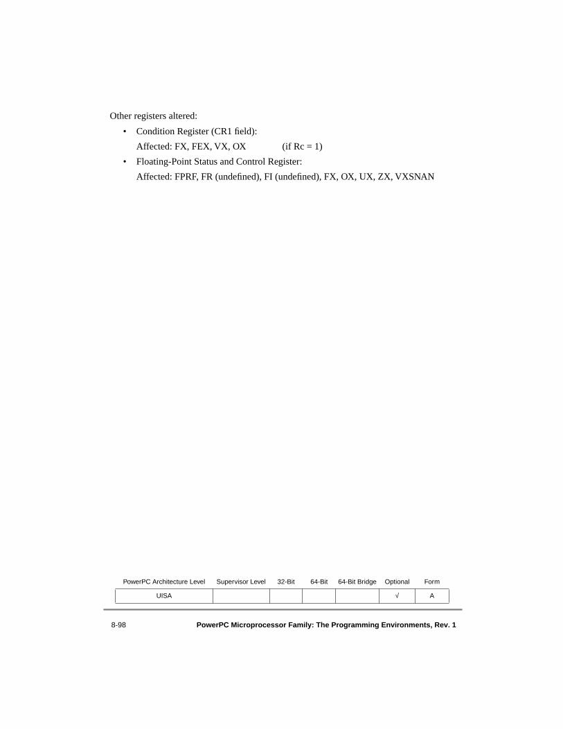
8-98 PowerPC Microprocessor Family: The Programming Environments, Rev. 1
Other registers altered:
• Condition Register (CR1 field):
Affected: FX, FEX, VX, OX (if Rc = 1)
• Floating-Point Status and Control Register:
Affected: FPRF, FR (undefined), FI (undefined), FX, OX, UX, ZX, VXSNAN
PowerPC Architecture Level Supervisor Level 32-Bit 64-Bit 64-Bit Bridge Optional Form
UISA √ A
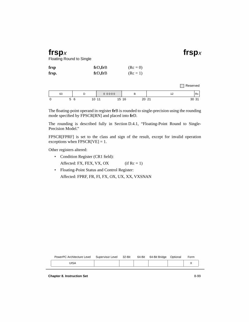
Chapter 8. Instruction Set 8-99
frspx frspxFloating Round to Single
frsp frD,frB (Rc = 0)frsp. frD,frB (Rc = 1)
The floating-point operand in register frB is rounded to single-precision using the roundingmode specified by FPSCR[RN] and placed into frD.
The rounding is described fully in Section D.4.1, “Floating-Point Round to Single-Precision Model.”
FPSCR[FPRF] is set to the class and sign of the result, except for invalid operationexceptions when FPSCR[VE] = 1.
Other registers altered:
• Condition Register (CR1 field):
Affected: FX, FEX, VX, OX (if Rc = 1)
• Floating-Point Status and Control Register:
Affected: FPRF, FR, FI, FX, OX, UX, XX, VXSNAN
PowerPC Architecture Level Supervisor Level 32-Bit 64-Bit 64-Bit Bridge Optional Form
UISA X
0 5 6 10 11 15 16 20 21 30 31
Reserved
B 12 Rc63 D 0 0 0 0 0

8-100 PowerPC Microprocessor Family: The Programming Environments, Rev. 1
frsqrtex frsqrtexFloating Reciprocal Square Root Estimate
frsqrte frD,frB (Rc = 0)frsqrte. frD,frB (Rc = 1)
A double-precision estimate of the reciprocal of the square root of the floating-pointoperand in register frB is placed into register frD. The estimate placed into register frD iscorrect to a precision of one part in 32 of the reciprocal of the square root of frB. That is,
where x is the initial value in frB. Note that the value placed into register frD may varybetween implementations, and between different executions on the same implementation.
Operation with various special values of the operand is summarized below:
Operand Result Exception
–∞ QNaN** VXSQRT
<0 QNaN** VXSQRT
–0 –∞* ZX
+0 +∞* ZX
+∞ +0 None
SNaN QNaN** VXSNAN
QNaN QNaN None
Notes: * No result if FPSCR[ZE] = 1
** No result if FPSCR[VE] = 1
FPSCR[FPRF] is set to the class and sign of the result, except for invalid operationexceptions when FPSCR[VE] = 1 and zero divide exceptions when FPSCR[ZE] = 1.
Note that no single-precision version of the frsqrte instruction is provided; however, bothfrB and frD are representable in single-precision format.
This instruction is optional in the PowerPC architecture.
0 5 6 10 11 15 16 20 21 25 26 30 31
Reserved
63 D 0 0 0 0 0 B 0 0 0 0 0 26 Rc
ABS
estimate1
x-------
–
1
x-------
--------------------------------------
132------≤

Chapter 8. Instruction Set 8-101
Other registers altered:
• Condition Register (CR1 field):
Affected: FX, FEX, VX, OX (if Rc = 1)
• Floating-Point Status and Control Register:
Affected: FPRF, FR (undefined), FI (undefined), FX, ZX, VXSNAN, VXSQRT
PowerPC Architecture Level Supervisor Level 32-Bit 64-Bit 64-Bit Bridge Optional Form
UISA √ A

8-102 PowerPC Microprocessor Family: The Programming Environments, Rev. 1
fselx fselxFloating Select
fsel frD,frA,frC,frB (Rc = 0)fsel. frD,frA,frC,frB (Rc = 1)
if (frA) ≥ 0.0 then frD ← (frC)else frD ← (frB)
The floating-point operand in register frA is compared to the value zero. If the operand isgreater than or equal to zero, register frD is set to the contents of register frC. If the operandis less than zero or is a NaN, register frD is set to the contents of register frB. Thecomparison ignores the sign of zero (that is, regards +0 as equal to –0).
Care must be taken in using fsel if IEEE compatibility is required, or if the values beingtested can be NaNs or infinities.
For examples of uses of this instruction, see Section D.3, “Floating-Point Conversions,”and Section D.5, “Floating-Point Selection.”
This instruction is optional in the PowerPC architecture.
Other registers altered:
• Condition Register (CR1 field):
Affected: FX, FEX, VX, OX (if Rc = 1)
PowerPC Architecture Level Supervisor Level 32-Bit 64-Bit 64-Bit Bridge Optional Form
UISA √ A
B C 23 Rc
0 5 6 10 11 15 16 20 21 25 26 30 31
63 D A
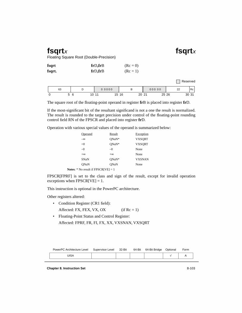
Chapter 8. Instruction Set 8-103
fsqrtx fsqrtxFloating Square Root (Double-Precision)
fsqrt frD,frB (Rc = 0)fsqrt. frD,frB (Rc = 1)
The square root of the floating-point operand in register frB is placed into register frD.
If the most-significant bit of the resultant significand is not a one the result is normalized.The result is rounded to the target precision under control of the floating-point roundingcontrol field RN of the FPSCR and placed into register frD.
Operation with various special values of the operand is summarized below:
Operand Result Exception
–∞ QNaN* VXSQRT
<0 QNaN* VXSQRT
–0 –0 None
+∞ +∞ None
SNaN QNaN* VXSNAN
QNaN QNaN None
Notes: * No result if FPSCR[VE] = 1
FPSCR[FPRF] is set to the class and sign of the result, except for invalid operationexceptions when FPSCR[VE] = 1.
This instruction is optional in the PowerPC architecture.
Other registers altered:
• Condition Register (CR1 field):
Affected: FX, FEX, VX, OX (if Rc = 1)
• Floating-Point Status and Control Register:
Affected: FPRF, FR, FI, FX, XX, VXSNAN, VXSQRT
PowerPC Architecture Level Supervisor Level 32-Bit 64-Bit 64-Bit Bridge Optional Form
UISA √ A
B 0 0 0 0 0 22 Rc
0 5 6 10 11 15 16 20 21 25 26 30 31
Reserved
63 D 0 0 0 0 0

8-104 PowerPC Microprocessor Family: The Programming Environments, Rev. 1
fsqrtsx fsqrtsxFloating Square Root Single
fsqrts frD,frB (Rc = 0)fsqrts. frD,frB (Rc = 1)
The square root of the floating-point operand in register frB is placed into register frD.
If the most-significant bit of the resultant significand is not a one the result is normalized.The result is rounded to the target precision under control of the floating-point roundingcontrol field RN of the FPSCR and placed into register frD.
Operation with various special values of the operand is summarized below.
Operand Result Exception
–∞ QNaN* VXSQRT
<0 QNaN* VXSQRT
–0 –0 None
+∞ +∞ None
SNaN QNaN* VXSNAN
QNaN QNaN None
Notes: * No result if FPSCR[VE] = 1
FPSCR[FPRF] is set to the class and sign of the result, except for invalid operationexceptions when FPSCR[VE] = 1.
This instruction is optional in the PowerPC architecture.
Other registers altered:
• Condition Register (CR1 field):
Affected: FX, FEX, VX, OX (if Rc = 1)
• Floating-Point Status and Control Register:
Affected: FPRF, FR, FI, FX, XX, VXSNAN, VXSQRT
PowerPC Architecture Level Supervisor Level 32-Bit 64-Bit 64-Bit Bridge Optional Form
UISA √ A
0 5 6 10 11 15 16 20 21 25 26 30 31
Reserved
59 D 0 0 0 0 0 B 0 0 0 0 0 22 Rc

Chapter 8. Instruction Set 8-105
fsubx fsubxFloating Subtract (Double-Precision)
fsub frD,frA,frB (Rc = 0)fsub. frD,frA,frB (Rc = 1)[POWER mnemonics: fs, fs.]
The floating-point operand in register frB is subtracted from the floating-point operand inregister frA. If the most-significant bit of the resultant significand is not a one, the result isnormalized. The result is rounded to double-precision under control of the floating-pointrounding control field RN of the FPSCR and placed into frD.
The execution of the fsub instruction is identical to that of fadd, except that the contents offrB participate in the operation with its sign bit (bit 0) inverted.
FPSCR[FPRF] is set to the class and sign of the result, except for invalid operationexceptions when FPSCR[VE] = 1.
Other registers altered:
• Condition Register (CR1 field):
Affected: FX, FEX, VX, OX (if Rc = 1)
• Floating-Point Status and Control Register:
Affected: FPRF, FR, FI, FX, OX, UX, XX, VXSNAN, VXISI
PowerPC Architecture Level Supervisor Level 32-Bit 64-Bit 64-Bit Bridge Optional Form
UISA A
0 5 6 10 11 15 16 20 21 25 26 30 31
Reserved
B 0 0 0 0 0 20 Rc63 D A
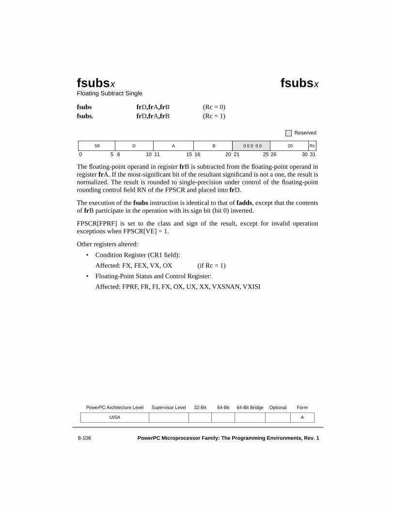
8-106 PowerPC Microprocessor Family: The Programming Environments, Rev. 1
fsubsx fsubsxFloating Subtract Single
fsubs frD,frA,frB (Rc = 0)fsubs. frD,frA,frB (Rc = 1)
The floating-point operand in register frB is subtracted from the floating-point operand inregister frA. If the most-significant bit of the resultant significand is not a one, the result isnormalized. The result is rounded to single-precision under control of the floating-pointrounding control field RN of the FPSCR and placed into frD.
The execution of the fsubs instruction is identical to that of fadds, except that the contentsof frB participate in the operation with its sign bit (bit 0) inverted.
FPSCR[FPRF] is set to the class and sign of the result, except for invalid operationexceptions when FPSCR[VE] = 1.
Other registers altered:
• Condition Register (CR1 field):
Affected: FX, FEX, VX, OX (if Rc = 1)
• Floating-Point Status and Control Register:
Affected: FPRF, FR, FI, FX, OX, UX, XX, VXSNAN, VXISI
PowerPC Architecture Level Supervisor Level 32-Bit 64-Bit 64-Bit Bridge Optional Form
UISA A
0 5 6 10 11 15 16 20 21 25 26 30 31
Reserved
B 0 0 0 0 0 20 Rc59 D A

Chapter 8. Instruction Set 8-107
icbi icbiInstruction Cache Block Invalidate
icbi rA,rB
EA is the sum (rA|0) + (rB).
If the block containing the byte addressed by EA is in coherency-required mode, and ablock containing the byte addressed by EA is in the instruction cache of any processor, theblock is made invalid in all such instruction caches, so that subsequent references cause theblock to be refetched.
If the block containing the byte addressed by EA is in coherency-not-required mode, and ablock containing the byte addressed by EA is in the instruction cache of this processor, theblock is made invalid in that instruction cache, so that subsequent references cause theblock to be refetched.
The function of this instruction is independent of the write-through, write-back, andcaching-inhibited/allowed modes of the block containing the byte addressed by EA.
This instruction is treated as a load from the addressed byte with respect to addresstranslation and memory protection. It may also be treated as a load for referenced andchanged bit recording except that referenced and changed bit recording may not occur.Implementations with a combined data and instruction cache treat the icbi instruction as ano-op, except that they may invalidate the target block in the instruction caches of otherprocessors if the block is in coherency-required mode.
The icbi instruction invalidates the block at EA (rA|0 + rB). If the processor is amultiprocessor implementation (for example, the 601, 604, or 620) and the block is markedcoherency-required, the processor will send an address-only broadcast to other processorscausing those processors to invalidate the block from their instruction caches.
For faster processing, many implementations will not compare the entire EA (rA|0 + rB)with the tag in the instruction cache. Instead, they will use the bits in the EA to locate theset that the block is in, and invalidate all blocks in that set.
Other registers altered:
• None
PowerPC Architecture Level Supervisor Level 32-Bit 64-Bit 64-Bit Bridge Optional Form
VEA X
0 5 6 10 11 15 16 20 21 30 31
Reserved
B 982 031 0 0 0 0 0 A
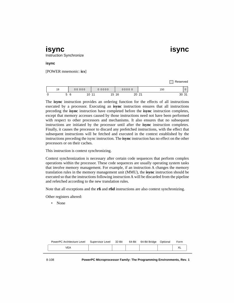
8-108 PowerPC Microprocessor Family: The Programming Environments, Rev. 1
isync isyncInstruction Synchronize
isync
[POWER mnemonic: ics]
The isync instruction provides an ordering function for the effects of all instructionsexecuted by a processor. Executing an isync instruction ensures that all instructionspreceding the isync instruction have completed before the isync instruction completes,except that memory accesses caused by those instructions need not have been performedwith respect to other processors and mechanisms. It also ensures that no subsequentinstructions are initiated by the processor until after the isync instruction completes.Finally, it causes the processor to discard any prefetched instructions, with the effect thatsubsequent instructions will be fetched and executed in the context established by theinstructions preceding the isync instruction. The isync instruction has no effect on the otherprocessors or on their caches.
This instruction is context synchronizing.
Context synchronization is necessary after certain code sequences that perform complexoperations within the processor. These code sequences are usually operating system tasksthat involve memory management. For example, if an instruction A changes the memorytranslation rules in the memory management unit (MMU), the isync instruction should beexecuted so that the instructions following instruction A will be discarded from the pipelineand refetched according to the new translation rules.
Note that all exceptions and the rfi and rfid instructions are also context synchronizing.
Other registers altered:
• None
PowerPC Architecture Level Supervisor Level 32-Bit 64-Bit 64-Bit Bridge Optional Form
VEA XL
0 0 0 0 0 150 0
0 5 6 10 11 15 16 20 21 30 31
Reserved
19 0 0 0 0 0 0 0 0 0 0
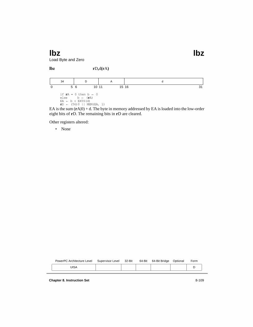
Chapter 8. Instruction Set 8-109
lbz lbzLoad Byte and Zero
lbz rD,d(rA)
if rA = 0 then b ← 0else b ← (rA)EA ← b + EXTS(d)rD ← (56)0 || MEM(EA, 1)
EA is the sum (rA|0) + d. The byte in memory addressed by EA is loaded into the low-ordereight bits of rD. The remaining bits in rD are cleared.
Other registers altered:
• None
PowerPC Architecture Level Supervisor Level 32-Bit 64-Bit 64-Bit Bridge Optional Form
UISA D
0 5 6 10 11 15 16 31
d34 D A

8-110 PowerPC Microprocessor Family: The Programming Environments, Rev. 1
lbzu lbzuLoad Byte and Zero with Update
lbzu rD,d(rA)
EA ← (rA) + EXTS(d)rD ← (56)0 || MEM(EA, 1)rA ← EA
EA is the sum (rA) + d. The byte in memory addressed by EA is loaded into the low-ordereight bits of rD. The remaining bits in rD are cleared.
EA is placed into rA.
If rA = 0, or rA = rD, the instruction form is invalid.
Other registers altered:
• None
PowerPC Architecture Level Supervisor Level 32-Bit 64-Bit 64-Bit Bridge Optional Form
UISA D
0 5 6 10 11 15 16 31
d35 D A
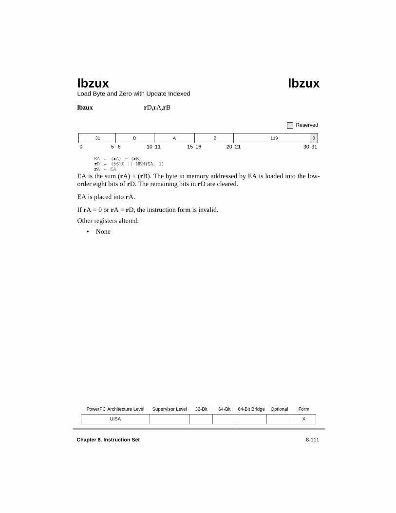
Chapter 8. Instruction Set 8-111
lbzux lbzuxLoad Byte and Zero with Update Indexed
lbzux rD,rA,rB
EA ← (rA) + (rB)rD ← (56)0 || MEM(EA, 1)rA ← EA
EA is the sum (rA) + (rB). The byte in memory addressed by EA is loaded into the low-order eight bits of rD. The remaining bits in rD are cleared.
EA is placed into rA.
If rA = 0 or rA = rD, the instruction form is invalid.
Other registers altered:
• None
PowerPC Architecture Level Supervisor Level 32-Bit 64-Bit 64-Bit Bridge Optional Form
UISA X
0 5 6 10 11 15 16 20 21 30 31
Reserved
B 119 031 D A

8-112 PowerPC Microprocessor Family: The Programming Environments, Rev. 1
lbzx lbzxLoad Byte and Zero Indexed
lbzx rD,rA,rB
if rA = 0 then b ← 0else b ← (rA)EA ← b + (rB)rD ← (56)0 || MEM(EA, 1)
EA is the sum (rA|0) + (rB). The byte in memory addressed by EA is loaded into the low-order eight bits of rD. The remaining bits in rD are cleared.
Other registers altered:
• None
PowerPC Architecture Level Supervisor Level 32-Bit 64-Bit 64-Bit Bridge Optional Form
UISA X
0 5 6 10 11 15 16 20 21 30 31
Reserved
B 87 031 D A

Chapter 8. Instruction Set 8-113
ld 64-Bit Implementations Only ldLoad Double Word
ld rD,ds(rA)
if rA = 0 then b ← 0else b ← (rA)EA ← b + EXTS(ds || 0b00)rD ← MEM(EA, 8)
EA is the sum (rA|0) + (ds || 0b00). The double word in memory addressed by EA is loadedinto rD.
This instruction is defined only for 64-bit implementations. Using it on a 32-bitimplementation will cause the system illegal instruction error handler to be invoked.
Other registers altered:
• None
PowerPC Architecture Level Supervisor Level 32-Bit 64-Bit 64-Bit Bridge Optional Form
UISA √ DS
0 5 6 10 11 15 16 29 30 31
58 D A ds 0 0
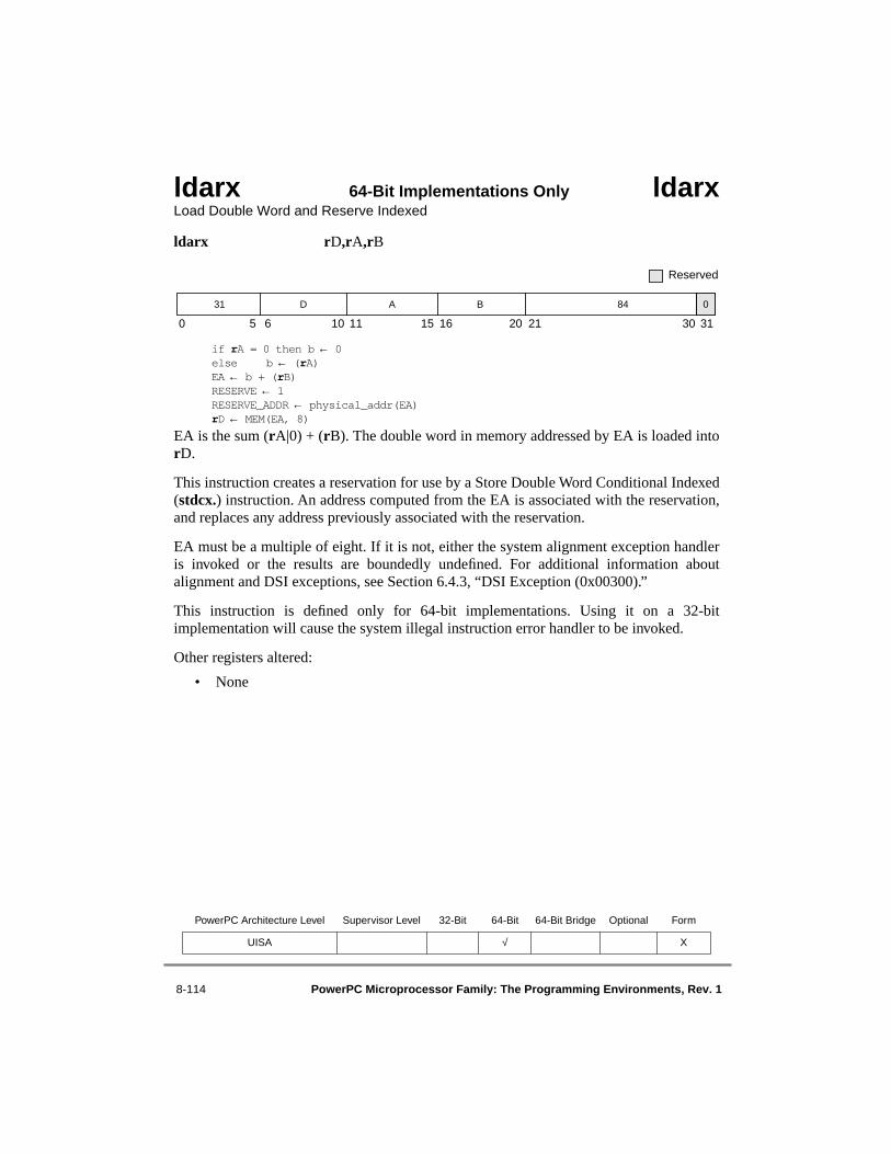
8-114 PowerPC Microprocessor Family: The Programming Environments, Rev. 1
ldarx 64-Bit Implementations Only ldarxLoad Double Word and Reserve Indexed
ldarx rD,rA,rB
if rA = 0 then b ← 0else b ← (rA)EA ← b + (rB)RESERVE ← 1RESERVE_ADDR ← physical_addr(EA)rD ← MEM(EA, 8)
EA is the sum (rA|0) + (rB). The double word in memory addressed by EA is loaded intorD.
This instruction creates a reservation for use by a Store Double Word Conditional Indexed(stdcx.) instruction. An address computed from the EA is associated with the reservation,and replaces any address previously associated with the reservation.
EA must be a multiple of eight. If it is not, either the system alignment exception handleris invoked or the results are boundedly undefined. For additional information aboutalignment and DSI exceptions, see Section 6.4.3, “DSI Exception (0x00300).”
This instruction is defined only for 64-bit implementations. Using it on a 32-bitimplementation will cause the system illegal instruction error handler to be invoked.
Other registers altered:
• None
PowerPC Architecture Level Supervisor Level 32-Bit 64-Bit 64-Bit Bridge Optional Form
UISA √ X
0 5 6 10 11 15 16 20 21 30 31
Reserved
31 D A B 84 0

Chapter 8. Instruction Set 8-115
ldu 64-Bit Implementations Only lduLoad Double Word with Update
ldu rD,ds(rA)
EA ← (rA) + EXTS(ds || 0b00)rD ← MEM(EA, 8)rA ← EA
EA is the sum (rA) + (ds || 0b00). The double word in memory addressed by EA is loadedinto rD.
EA is placed into rA.
If rA = 0 or rA = rD, the instruction form is invalid.
This instruction is defined only for 64-bit implementations. Using it on a 32-bitimplementation will cause the system illegal instruction error handler to be invoked.
Other registers altered:
• None
PowerPC Architecture Level Supervisor Level 32-Bit 64-Bit 64-Bit Bridge Optional Form
UISA √ DS
0 5 6 10 11 15 16 29 30 31
58 D A ds 0 1

8-116 PowerPC Microprocessor Family: The Programming Environments, Rev. 1
ldux 64-Bit Implementations Only lduxxLoad Double Word with Update Indexed
ldux rD,rA,rB
EA ← (rA) + (rB)rD ← MEM(EA, 8)rA ← EA
EA is the sum (rA) + (rB). The double word in memory addressed by EA is loaded into rD.
EA is placed into rA.
If rA = 0 or rA = rD, the instruction form is invalid.
This instruction is defined only for 64-bit implementations. Using it on a 32-bitimplementation will cause the system illegal instruction to be invoked.
Other registers altered:
• None
PowerPC Architecture Level Supervisor Level 32-Bit 64-Bit 64-Bit Bridge Optional Form
UISA √ X
0 5 6 10 11 15 16 20 21 30 31
Reserved
31 D A B 53 0
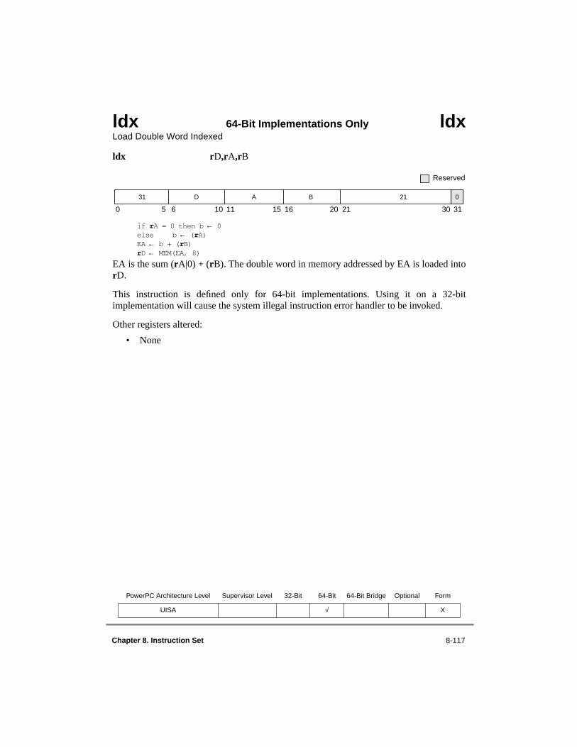
Chapter 8. Instruction Set 8-117
ldx 64-Bit Implementations Only ldxLoad Double Word Indexed
ldx rD,rA,rB
if rA = 0 then b ← 0else b ← (rA)EA ← b + (rB)rD ← MEM(EA, 8)
EA is the sum (rA|0) + (rB). The double word in memory addressed by EA is loaded intorD.
This instruction is defined only for 64-bit implementations. Using it on a 32-bitimplementation will cause the system illegal instruction error handler to be invoked.
Other registers altered:
• None
PowerPC Architecture Level Supervisor Level 32-Bit 64-Bit 64-Bit Bridge Optional Form
UISA √ X
0 5 6 10 11 15 16 20 21 30 31
Reserved
31 D A B 21 0
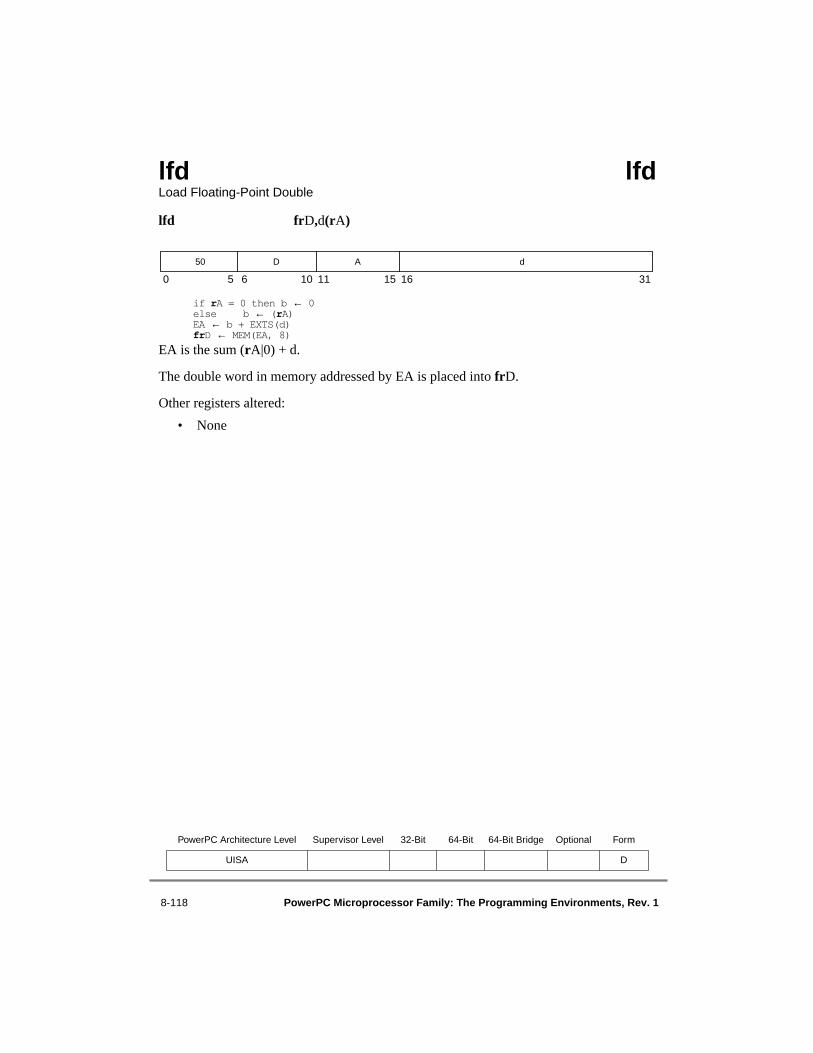
8-118 PowerPC Microprocessor Family: The Programming Environments, Rev. 1
lfd lfd Load Floating-Point Double
lfd frD,d(rA)
if rA = 0 then b ← 0else b ← (rA)EA ← b + EXTS(d)frD ← MEM(EA, 8)
EA is the sum (rA|0) + d.
The double word in memory addressed by EA is placed into frD.
Other registers altered:
• None
PowerPC Architecture Level Supervisor Level 32-Bit 64-Bit 64-Bit Bridge Optional Form
UISA D
0 5 6 10 11 15 16 31
d50 D A
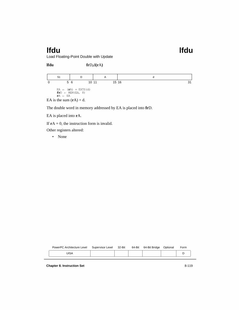
Chapter 8. Instruction Set 8-119
lfdu lfdu Load Floating-Point Double with Update
lfdu frD,d(rA)
EA ← (rA) + EXTS(d)frD ← MEM(EA, 8)rA ← EA
EA is the sum (rA) + d.
The double word in memory addressed by EA is placed into frD.
EA is placed into rA.
If rA = 0, the instruction form is invalid.
Other registers altered:
• None
PowerPC Architecture Level Supervisor Level 32-Bit 64-Bit 64-Bit Bridge Optional Form
UISA D
0 5 6 10 11 15 16 31
d51 D A
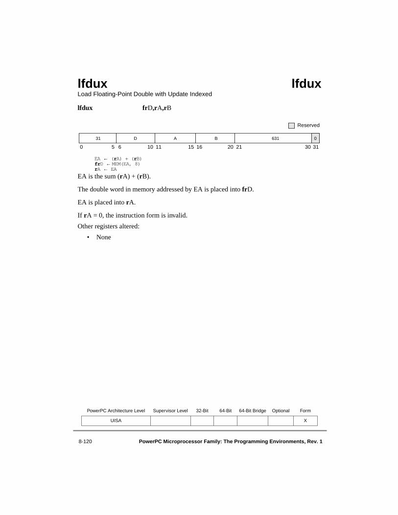
8-120 PowerPC Microprocessor Family: The Programming Environments, Rev. 1
lfdux lfdux Load Floating-Point Double with Update Indexed
lfdux frD,rA,rB
EA ← (rA) + (rB)frD ← MEM(EA, 8)rA ← EA
EA is the sum (rA) + (rB).
The double word in memory addressed by EA is placed into frD.
EA is placed into rA.
If rA = 0, the instruction form is invalid.
Other registers altered:
• None
PowerPC Architecture Level Supervisor Level 32-Bit 64-Bit 64-Bit Bridge Optional Form
UISA X
0 5 6 10 11 15 16 20 21 30 31
Reserved
B 631 031 D A

Chapter 8. Instruction Set 8-121
lfdx lfdx Load Floating-Point Double Indexed
lfdx frD,rA,rB
if rA = 0 then b ← 0else b ← (rA)EA ← b + (rB)frD ← MEM(EA, 8)
EA is the sum (rA|0) + (rB).
The double word in memory addressed by EA is placed into frD.
Other registers altered:
• None
PowerPC Architecture Level Supervisor Level 32-Bit 64-Bit 64-Bit Bridge Optional Form
UISA X
0 5 6 10 11 15 16 20 21 30 31
Reserved
B 599 031 D A

8-122 PowerPC Microprocessor Family: The Programming Environments, Rev. 1
lfs lfs Load Floating-Point Single
lfs frD,d(rA)
if rA = 0 then b ← 0else b ← (rA)EA ← b + EXTS(d)frD ← DOUBLE(MEM(EA, 4))
EA is the sum (rA|0) + d.
The word in memory addressed by EA is interpreted as a floating-point single-precisionoperand. This word is converted to floating-point double-precision (see Section D.6,“Floating-Point Load Instructions”) and placed into frD.
Other registers altered:
• None
PowerPC Architecture Level Supervisor Level 32-Bit 64-Bit 64-Bit Bridge Optional Form
UISA D
0 5 6 10 11 15 16 31
d48 D A

Chapter 8. Instruction Set 8-123
lfsu lfsu Load Floating-Point Single with Update
lfsu frD,d(rA)
EA ← (rA) + EXTS(d)frD ← DOUBLE(MEM(EA, 4))rA ← EA
EA is the sum (rA) + d.
The word in memory addressed by EA is interpreted as a floating-point single-precisionoperand. This word is converted to floating-point double-precision (see Section D.6,“Floating-Point Load Instructions”) and placed into frD.
EA is placed into rA.
If rA = 0, the instruction form is invalid.
Other registers altered:
• None
PowerPC Architecture Level Supervisor Level 32-Bit 64-Bit 64-Bit Bridge Optional Form
UISA D
0 5 6 10 11 15 16 31
d49 D A

8-124 PowerPC Microprocessor Family: The Programming Environments, Rev. 1
lfsux lfsux Load Floating-Point Single with Update Indexed
lfsux frD,rA,rB
EA ← (rA) + (rB)frD ← DOUBLE(MEM(EA, 4))rA ← EA
EA is the sum (rA) + (rB).
The word in memory addressed by EA is interpreted as a floating-point single-precisionoperand. This word is converted to floating-point double-precision (see Section D.6,“Floating-Point Load Instructions”) and placed into frD.
EA is placed into rA.
If rA = 0, the instruction form is invalid.
Other registers altered:
• None
PowerPC Architecture Level Supervisor Level 32-Bit 64-Bit 64-Bit Bridge Optional Form
UISA X
0 5 6 10 11 15 16 20 21 30 31
Reserved
B 567 031 D A

Chapter 8. Instruction Set 8-125
lfsx lfsx Load Floating-Point Single Indexed lfsx frD,rA,rB
if rA = 0 then b ← 0else b ← (rA)EA ← b + (rB)frD ← DOUBLE(MEM(EA, 4))
EA is the sum (rA|0) + (rB).
The word in memory addressed by EA is interpreted as a floating-point single-precisionoperand. This word is converted to floating-point double-precision (see Section D.6,“Floating-Point Load Instructions”) and placed into frD.
Other registers altered:
• None
PowerPC Architecture Level Supervisor Level 32-Bit 64-Bit 64-Bit Bridge Optional Form
UISA X
0 5 6 10 11 15 16 20 21 30 31
Reserved
B 535 031 D A
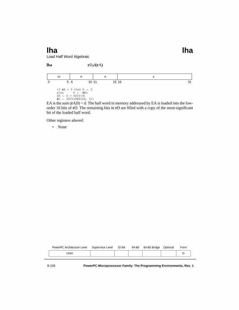
8-126 PowerPC Microprocessor Family: The Programming Environments, Rev. 1
lha lha Load Half Word Algebraic
lha rD,d(rA)
if rA = 0 then b ← 0else b ← (rA)EA ← b + EXTS(d)rD ← EXTS(MEM(EA, 2))
EA is the sum (rA|0) + d. The half word in memory addressed by EA is loaded into the low-order 16 bits of rD. The remaining bits in rD are filled with a copy of the most-significantbit of the loaded half word.
Other registers altered:
• None
PowerPC Architecture Level Supervisor Level 32-Bit 64-Bit 64-Bit Bridge Optional Form
UISA D
0 5 6 10 11 15 16 31
d42 D A

Chapter 8. Instruction Set 8-127
lhau lhauLoad Half Word Algebraic with Update
lhau rD,d(rA)
EA ← (rA) + EXTS(d)rD ← EXTS(MEM(EA, 2))rA ← EA
EA is the sum (rA) + d. The half word in memory addressed by EA is loaded into the low-order 16 bits of rD. The remaining bits in rD are filled with a copy of the most-significantbit of the loaded half word.
EA is placed into rA.
If rA = 0 or rA = rD, the instruction form is invalid.
Other registers altered:
• None
PowerPC Architecture Level Supervisor Level 32-Bit 64-Bit 64-Bit Bridge Optional Form
UISA D
0 5 6 10 11 15 16 31
d43 D A

8-128 PowerPC Microprocessor Family: The Programming Environments, Rev. 1
lhaux lhauxLoad Half Word Algebraic with Update Indexed
lhaux rD,rA,rB
EA ← (rA) + (rB)rD ← EXTS(MEM(EA, 2))rA ← EA
EA is the sum (rA) + (rB). The half word in memory addressed by EA is loaded into thelow-order 16 bits of rD. The remaining bits in rD are filled with a copy of the most-significant bit of the loaded half word.
EA is placed into rA.
If rA = 0 or rA = rD, the instruction form is invalid.
Other registers altered:
• None
PowerPC Architecture Level Supervisor Level 32-Bit 64-Bit 64-Bit Bridge Optional Form
UISA X
0 5 6 10 11 15 16 20 21 30 31
Reserved
B 375 031 D A

Chapter 8. Instruction Set 8-129
lhax lhaxLoad Half Word Algebraic Indexed
lhax rD,rA,rB
if rA = 0 then b ← 0else b ← (rA)EA ← b + (rB)rD ← EXTS(MEM(EA, 2))
EA is the sum (rA|0) + (rB). The half word in memory addressed by EA is loaded into thelow-order 16 bits of rD. The remaining bits in rD are filled with a copy of the most-significant bit of the loaded half word.
Other registers altered:
• None
PowerPC Architecture Level Supervisor Level 32-Bit 64-Bit 64-Bit Bridge Optional Form
UISA X
0 5 6 10 11 15 16 20 21 30 31
Reserved
B 343 031 D A

8-130 PowerPC Microprocessor Family: The Programming Environments, Rev. 1
lhbrx lhbrxLoad Half Word Byte-Reverse Indexed
lhbrx rD,rA,rB
if rA = 0 then b ← 0else b ← (rA)EA ← b + (rB)rD ← (48)0 || MEM(EA + 1, 1) || MEM(EA, 1)
EA is the sum (rA|0) + (rB). Bits 0–7 of the half word in memory addressed by EA areloaded into the low-order eight bits of rD. Bits 8–15 of the half word in memory addressedby EA are loaded into the subsequent low-order eight bits of rD. The remaining bits in rDare cleared.
The PowerPC architecture cautions programmers that some implementations of thearchitecture may run the lhbrx instructions with greater latency than other types of loadinstructions.
Other registers altered:
• None
PowerPC Architecture Level Supervisor Level 32-Bit 64-Bit 64-Bit Bridge Optional Form
UISA X
0 5 6 10 11 15 16 20 21 30 31
Reserved
B 790 031 D A

Chapter 8. Instruction Set 8-131
lhz lhzLoad Half Word and Zero
lhz rD,d(rA)
if rA = 0 then b ← 0else b ← (rA)EA ← b + EXTS(d)rD ← (48)0 || MEM(EA, 2)
EA is the sum (rA|0) + d. The half word in memory addressed by EA is loaded into the low-order 16 bits of rD. The remaining bits in rD are cleared.
Other registers altered:
• None
PowerPC Architecture Level Supervisor Level 32-Bit 64-Bit 64-Bit Bridge Optional Form
UISA D
0 5 6 10 11 15 16 31
d40 D A

8-132 PowerPC Microprocessor Family: The Programming Environments, Rev. 1
lhzu lhzuLoad Half Word and Zero with Update
lhzu rD,d(rA)
EA ← rA + EXTS(d)rD ← (48)0 || MEM(EA, 2)rA ← EA
EA is the sum (rA) + d. The half word in memory addressed by EA is loaded into the low-order 16 bits of rD. The remaining bits in rD are cleared.
EA is placed into rA.
If rA = 0 or rA = rD, the instruction form is invalid.
Other registers altered:
• None
PowerPC Architecture Level Supervisor Level 32-Bit 64-Bit 64-Bit Bridge Optional Form
UISA D
0 5 6 10 11 15 16 31
d41 D A

Chapter 8. Instruction Set 8-133
lhzux lhzuxLoad Half Word and Zero with Update Indexed
lhzux rD,rA,rB
EA ← (rA) + (rB)rD ← (48)0 || MEM(EA, 2)rA ← EA
EA is the sum (rA) + (rB). The half word in memory addressed by EA is loaded into thelow-order 16 bits of rD. The remaining bits in rD are cleared.
EA is placed into rA.
If rA = 0 or rA = rD, the instruction form is invalid.
Other registers altered:
• None
PowerPC Architecture Level Supervisor Level 32-Bit 64-Bit 64-Bit Bridge Optional Form
UISA X
0 5 6 10 11 15 16 20 21 30 31
Reserved
B 311 031 D A
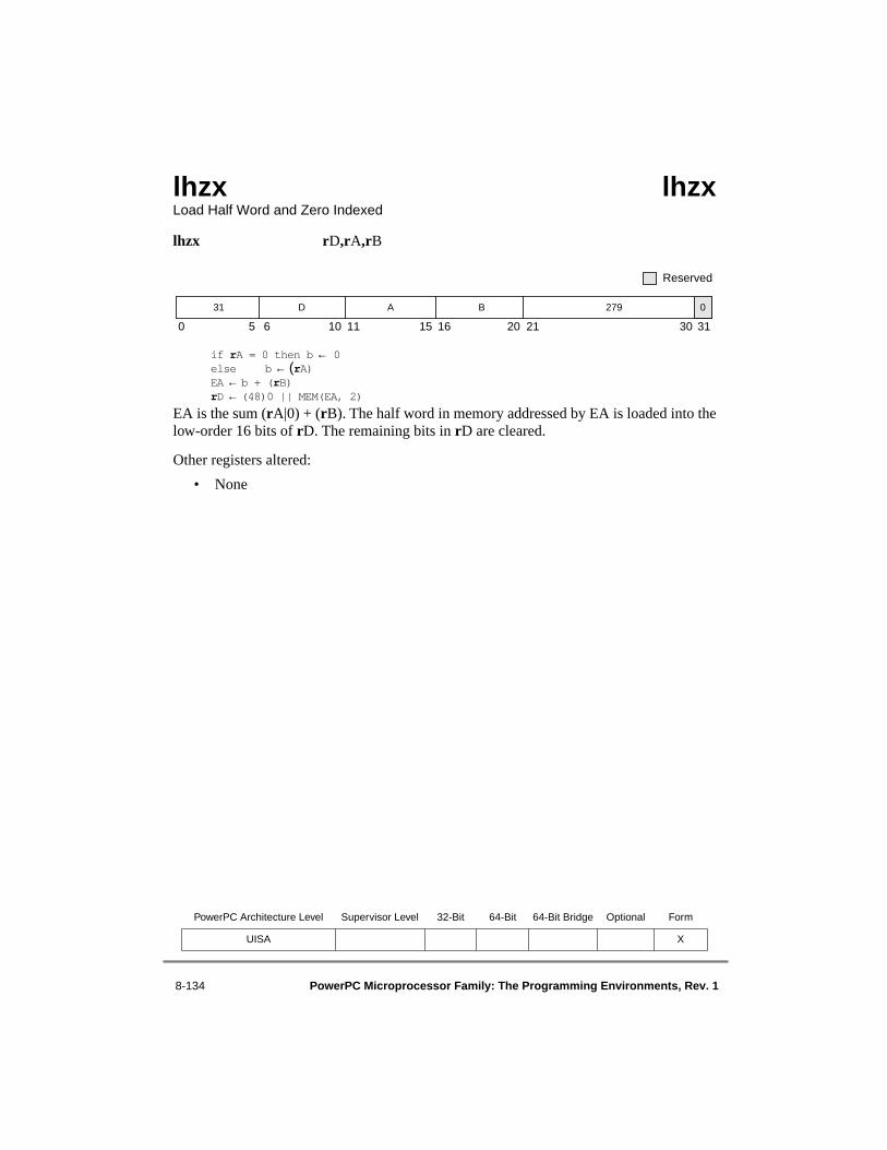
8-134 PowerPC Microprocessor Family: The Programming Environments, Rev. 1
lhzx lhzxLoad Half Word and Zero Indexed
lhzx rD,rA,rB
if rA = 0 then b ← 0else b ← (rA)EA ← b + (rB)rD ← (48)0 || MEM(EA, 2)
EA is the sum (rA|0) + (rB). The half word in memory addressed by EA is loaded into thelow-order 16 bits of rD. The remaining bits in rD are cleared.
Other registers altered:
• None
PowerPC Architecture Level Supervisor Level 32-Bit 64-Bit 64-Bit Bridge Optional Form
UISA X
0 5 6 10 11 15 16 20 21 30 31
Reserved
B 279 031 D A

Chapter 8. Instruction Set 8-135
lmw lmwLoad Multiple Word
lmw rD,d(rA)
[POWER mnemonic: lm]
if rA = 0 then b ← 0else b ← (rA)EA ← b + EXTS(d)r ← rDdo while r ≤ 31
GPR(r) ← (32)0 || MEM(EA, 4)r ← r + 1EA ← EA + 4
EA is the sum (rA|0) + d.
n = (32 – rD).
n consecutive words starting at EA are loaded into the low-order 32 bits of GPRs rDthrough r31. The high-order 32 bits of these GPRs are cleared.
EA must be a multiple of four. If it is not, either the system alignment exception handler isinvoked or the results are boundedly undefined. For additional information about alignmentand DSI exceptions, see Section 6.4.3, “DSI Exception (0x00300).”
If rA is in the range of registers specified to be loaded, including the case in which rA = 0,the instruction form is invalid.
Note that, in some implementations, this instruction is likely to have a greater latency andtake longer to execute, perhaps much longer, than a sequence of individual load or storeinstructions that produce the same results.
Other registers altered:
• None
PowerPC Architecture Level Supervisor Level 32-Bit 64-Bit 64-Bit Bridge Optional Form
UISA D
0 5 6 10 11 15 16 31
d46 D A

8-136 PowerPC Microprocessor Family: The Programming Environments, Rev. 1
lswi lswiLoad String Word Immediate
lswi rD,rA,NB
[POWER mnemonic: lsi]
if rA = 0 then EA ← 0else EA ← (rA)if NB = 0 then n ← 32elsen ← NBr ← rD – 1i ← 32do while n > 0
if i = 32 thenr ← r + 1 (mod 32)GPR(r) ← 0
GPR(r)[i–i + 7] ← MEM(EA, 1)i ← i + 8if i = 64 then i ← 32EA ← EA + 1n ← n – 1
EA is (rA|0).
Let n = NB if NB ≠ 0, n = 32 if NB = 0; n is the number of bytes to load. Let nr = CEIL(n ÷ 4); nr is the number of registers to be loaded with data.
n consecutive bytes starting at EA are loaded into GPRs rD through rD + nr – 1. Data isloaded into the low-order four bytes of each GPR; the high-order four bytes are cleared.
Bytes are loaded left to right in each register. The sequence of registers wraps around to r0if required. If the low-order 4 bytes of register rD + nr – 1 are only partially filled, theunfilled low-order byte(s) of that register are cleared.
If rA is in the range of registers specified to be loaded, including the case in which rA = 0,the instruction form is invalid.
Under certain conditions (for example, segment boundary crossing) the data alignmentexception handler may be invoked. For additional information about data alignmentexceptions, see Section 6.4.3, “DSI Exception (0x00300).”
0 5 6 10 11 15 16 20 21 30 31
Reserved
NB 597 031 D A

Chapter 8. Instruction Set 8-137
Note that, in some implementations, this instruction is likely to have greater latency andtake longer to execute, perhaps much longer, than a sequence of individual load or storeinstructions that produce the same results.
Other registers altered:
• None
PowerPC Architecture Level Supervisor Level 32-Bit 64-Bit 64-Bit Bridge Optional Form
UISA X

8-138 PowerPC Microprocessor Family: The Programming Environments, Rev. 1
lswx lswxLoad String Word Indexed
lswx rD,rA,rB
[POWER mnemonic: lsx]
if rA = 0 then b ← 0else b ← (rA)EA ← b + (rB)n ← XER[25–31]r ← rD – 1i ← 32rD ← undefined do while n > 0if i = 32 thenr ← r + 1 (mod 32)GPR(r) ← 0
GPR(r)[i–i + 7] ← MEM(EA, 1)i ← i + 8if i = 64 then i ← 32EA ← EA + 1n ← n – 1
EA is the sum (rA|0) + (rB). Let n = XER[25–31]; n is the number of bytes to load. Let nr = CEIL(n ÷ 4); nr is the number of registers to receive data. If n > 0, n consecutive bytesstarting at EA are loaded into GPRs rD through rD + nr – 1. Data is loaded into the low-order four bytes of each GPR; the high-order four bytes are cleared.
Bytes are loaded left to right in each register. The sequence of registers wraps aroundthrough r0 if required. If the low-order four bytes of rD + nr – 1 are only partially filled,the unfilled low-order byte(s) of that register are cleared. If n = 0, the contents of rD areundefined.
If rA or rB is in the range of registers specified to be loaded, including the case in whichrA = 0, either the system illegal instruction error handler is invoked or the results areboundedly undefined.
If rD = rA or rD = rB, the instruction form is invalid.
If rD and rA both specify GPR0, the form is invalid.
0 5 6 10 11 15 16 20 21 30 31
Reserved
B 533 031 D A

Chapter 8. Instruction Set 8-139
Under certain conditions (for example, segment boundary crossing) the data alignmentexception handler may be invoked. For additional information about data alignmentexceptions, see Section 6.4.3, “DSI Exception (0x00300).”
Note that, in some implementations, this instruction is likely to have a greater latency andtake longer to execute, perhaps much longer, than a sequence of individual load or storeinstructions that produce the same results.
Other registers altered:
• None
PowerPC Architecture Level Supervisor Level 32-Bit 64-Bit 64-Bit Bridge Optional Form
UISA X

8-140 PowerPC Microprocessor Family: The Programming Environments, Rev. 1
lwa 64-Bit Implementations Only lwaLoad Word Algebraic
lwa rD,ds(rA)
if rA = 0 then b ← 0else b ← (rA)EA ← b + EXTS(ds || 0b00)rD ← EXTS(MEM(EA, 4))
EA is the sum (rA|0) + (ds || 0b00). The word in memory addressed by EA is loaded intothe low-order 32 bits of rD. The contents of the high-order 32 bits of rD are filled with acopy of bit 0 of the loaded word.
This instruction is defined only for 64-bit implementations. Using it on a 32-bitimplementation will cause the system illegal instruction error handler to be invoked.
Other registers altered:
• None
PowerPC Architecture Level Supervisor Level 32-Bit 64-Bit 64-Bit Bridge Optional Form
UISA √ DS
0 5 6 10 11 15 16 29 30 31
58 D A ds 1 0
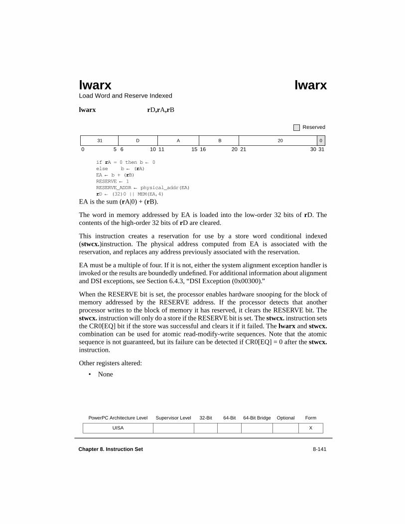
Chapter 8. Instruction Set 8-141
lwarx lwarxLoad Word and Reserve Indexed
lwarx rD,rA,rB
if rA = 0 then b ← 0else b ← (rA)EA ← b + (rB)RESERVE ← 1RESERVE_ADDR ← physical_addr(EA)rD ← (32)0 || MEM(EA,4)
EA is the sum (rA|0) + (rB).
The word in memory addressed by EA is loaded into the low-order 32 bits of rD. Thecontents of the high-order 32 bits of rD are cleared.
This instruction creates a reservation for use by a store word conditional indexed(stwcx.)instruction. The physical address computed from EA is associated with thereservation, and replaces any address previously associated with the reservation.
EA must be a multiple of four. If it is not, either the system alignment exception handler isinvoked or the results are boundedly undefined. For additional information about alignmentand DSI exceptions, see Section 6.4.3, “DSI Exception (0x00300).”
When the RESERVE bit is set, the processor enables hardware snooping for the block ofmemory addressed by the RESERVE address. If the processor detects that anotherprocessor writes to the block of memory it has reserved, it clears the RESERVE bit. Thestwcx. instruction will only do a store if the RESERVE bit is set. The stwcx. instruction setsthe CR0[EQ] bit if the store was successful and clears it if it failed. The lwarx and stwcx.combination can be used for atomic read-modify-write sequences. Note that the atomicsequence is not guaranteed, but its failure can be detected if CR0[EQ] = 0 after the stwcx.instruction.
Other registers altered:
• None
PowerPC Architecture Level Supervisor Level 32-Bit 64-Bit 64-Bit Bridge Optional Form
UISA X
0 5 6 10 11 15 16 20 21 30 31
Reserved
B 20 031 D A

8-142 PowerPC Microprocessor Family: The Programming Environments, Rev. 1
lwaux 64-Bit Implementations Only lwauxLoad Word Algebraic with Update Indexed
lwaux rD,rA,rB
EA ← (rA) + (rB)rD ← EXTS(MEM(EA, 4))rA ← EA
EA is the sum (rA) + (rB). The word in memory addressed by EA is loaded into the low-order 32 bits of rD. The high-order 32 bits of rD are filled with a copy of bit 0 of the loadedword.
EA is placed into rA.
If rA = 0 or rA = rD, the instruction form is invalid.
This instruction is defined only for 64-bit implementations. Using it on a 32-bitimplementation will cause the system illegal instruction error handler to be invoked.
Other registers altered:
• None
PowerPC Architecture Level Supervisor Level 32-Bit 64-Bit 64-Bit Bridge Optional Form
UISA √ X
0 5 6 10 11 15 16 20 21 30 31
Reserved
31 D A B 373 0

Chapter 8. Instruction Set 8-143
lwax 64-Bit Implementations Only lwaxLoad Word Algebraic Indexed
lwax rD,rA,rB
if rA = 0 then b ← 0else b ← (rA)EA ← b + (rB)rD ← EXTS(MEM(EA, 4))
EA is the sum (rA|0) + (rB). The word in memory addressed by EA is loaded into the low-order 32 bits of rD. The high-order 32 bits of rD are filled with a copy of bit 0 of the loadedword.
This instruction is defined only for 64-bit implementations. Using it on a 32-bitimplementation will cause the system illegal instruction error handler to be invoked.
Other registers altered:
• None
PowerPC Architecture Level Supervisor Level 32-Bit 64-Bit 64-Bit Bridge Optional Form
UISA √ X
0 5 6 10 11 15 16 20 21 30 31
Reserved
31 D A B 341 0
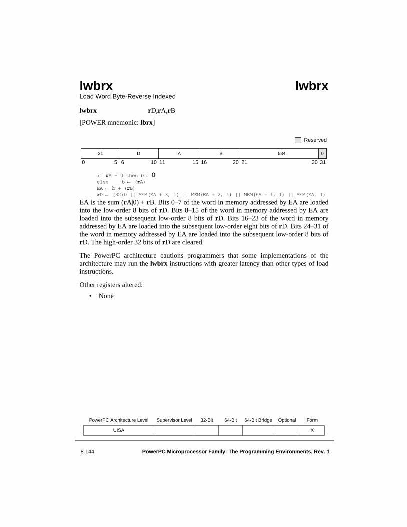
8-144 PowerPC Microprocessor Family: The Programming Environments, Rev. 1
lwbrx lwbrxLoad Word Byte-Reverse Indexed
lwbrx rD,rA,rB
[POWER mnemonic: lbrx]
if rA = 0 then b ← 0else b ← (rA)EA ← b + (rB)rD ← (32)0 || MEM(EA + 3, 1) || MEM(EA + 2, 1) || MEM(EA + 1, 1) || MEM(EA, 1)
EA is the sum (rA|0) + rB. Bits 0–7 of the word in memory addressed by EA are loadedinto the low-order 8 bits of rD. Bits 8–15 of the word in memory addressed by EA areloaded into the subsequent low-order 8 bits of rD. Bits 16–23 of the word in memoryaddressed by EA are loaded into the subsequent low-order eight bits of rD. Bits 24–31 ofthe word in memory addressed by EA are loaded into the subsequent low-order 8 bits ofrD. The high-order 32 bits of rD are cleared.
The PowerPC architecture cautions programmers that some implementations of thearchitecture may run the lwbrx instructions with greater latency than other types of loadinstructions.
Other registers altered:
• None
PowerPC Architecture Level Supervisor Level 32-Bit 64-Bit 64-Bit Bridge Optional Form
UISA X
0 5 6 10 11 15 16 20 21 30 31
Reserved
B 534 031 D A

Chapter 8. Instruction Set 8-145
lwz lwzLoad Word and Zero
lwz rD,d(rA)
[POWER mnemonic: l]
if rA = 0 then b ← 0else b ← (rA)EA ← b + EXTS(d)rD ← (32)0 || MEM(EA, 4)
EA is the sum (rA|0) + d. The word in memory addressed by EA is loaded into the low-order 32 bits of rD. The high-order 32 bits of rD are cleared.
Other registers altered:
• None
PowerPC Architecture Level Supervisor Level 32-Bit 64-Bit 64-Bit Bridge Optional Form
UISA D
0 5 6 10 11 15 16 31
d32 D A

8-146 PowerPC Microprocessor Family: The Programming Environments, Rev. 1
lwzu lwzuLoad Word and Zero with Update
lwzu rD,d(rA)
[POWER mnemonic: lu]
EA ← rA + EXTS(d)rD ← (32)0 || MEM(EA, 4)rA ← EA
EA is the sum (rA) + d. The word in memory addressed by EA is loaded into the low-order32 bits of rD. The high-order 32 bits of rD are cleared.
EA is placed into rA.
If rA = 0, or rA = rD, the instruction form is invalid.
Other registers altered:
• None
PowerPC Architecture Level Supervisor Level 32-Bit 64-Bit 64-Bit Bridge Optional Form
UISA D
0 5 6 10 11 15 16 31
d33 D A

Chapter 8. Instruction Set 8-147
lwzux lwzuxLoad Word and Zero with Update Indexed
lwzux rD,rA,rB[POWER mnemonic: lux]
EA ← (rA) + (rB)rD ← (32)0 || MEM(EA, 4)rA ← EA
EA is the sum (rA) + (rB). The word in memory addressed by EA is loaded into the low-order 32 bits of rD. The high-order 32 bits of rD are cleared.
EA is placed into rA.
If rA = 0, or rA = rD, the instruction form is invalid.
Other registers altered:
• None
PowerPC Architecture Level Supervisor Level 32-Bit 64-Bit 64-Bit Bridge Optional Form
UISA X
0 5 6 10 11 15 16 20 21 30 31
Reserved
B 55 031 D A

8-148 PowerPC Microprocessor Family: The Programming Environments, Rev. 1
lwzx lwzxLoad Word and Zero Indexed
lwzx rD,rA,rB
[POWER mnemonic: lx]
if rA = 0 then b ← 0else b ← (rA)EA ← b + rBrD ← (32)0 || MEM(EA, 4)
EA is the sum (rA|0) + (rB). The word in memory addressed by EA is loaded into the low-order 32 bits of rD. The high-order 32 bits of rD are cleared.
Other registers altered:
• None
PowerPC Architecture Level Supervisor Level 32-Bit 64-Bit 64-Bit Bridge Optional Form
UISA X
0 5 6 10 11 15 16 20 21 30 31
Reserved
B 23 031 D A

Chapter 8. Instruction Set 8-149
mcrf mcrfMove Condition Register Field
mcrf crfD,crfS
CR[4 ∗ crfD–4 ∗ crfD + 3] ← CR[4 ∗ crfS–4 ∗ crfS + 3]The contents of condition register field crfS are copied into condition register field crfD.All other condition register fields remain unchanged.
Other registers altered:
• Condition Register (CR field specified by operand crfD):
Affected: LT, GT, EQ, SO
PowerPC Architecture Level Supervisor Level 32-Bit 64-Bit 64-Bit Bridge Optional Form
UISA XL
0 5 6 8 9 10 11 13 14 15 16 20 21 30 31
Reserved
19 crfD 0 0 crfS 0 0 0 0 0 0 0 0 0 0 0 0 0 0 0 0 0 0

8-150 PowerPC Microprocessor Family: The Programming Environments, Rev. 1
mcrfs mcrfsMove to Condition Register from FPSCR
mcrfs crfD,crfS
The contents of FPSCR field crfS are copied to CR field crfD. All exception bits copied(except FEX and VX) are cleared in the FPSCR.
Other registers altered:
• Condition Register (CR field specified by operand crfD):
Affected: FX, FEX, VX, OX
• Floating-Point Status and Control Register:
Affected: FX, OX (if crfS = 0)
Affected: UX, ZX, XX, VXSNAN (if crfS = 1)
Affected: VXISI, VXIDI, VXZDZ, VXIMZ (if crfS = 2)
Affected: VXVC (if crfS = 3)
Affected: VXSOFT, VXSQRT, VXCVI (if crfS = 5)
PowerPC Architecture Level Supervisor Level 32-Bit 64-Bit 64-Bit Bridge Optional Form
UISA X
0 5 6 8 9 10 11 13 14 15 16 20 21 30 31
Reserved
63 crfD 0 0 crfS 0 0 0 0 0 0 0 64 0
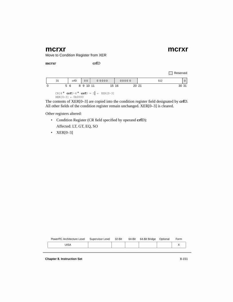
Chapter 8. Instruction Set 8-151
mcrxr mcrxrMove to Condition Register from XER
mcrxr crfD
CR[4 ∗ crfD–4 ∗ crfD + 3] ← XER[0–3]XER[0–3] ← 0b0000
The contents of XER[0–3] are copied into the condition register field designated by crfD.All other fields of the condition register remain unchanged. XER[0–3] is cleared.
Other registers altered:
• Condition Register (CR field specified by operand crfD):
Affected: LT, GT, EQ, SO
• XER[0–3]
PowerPC Architecture Level Supervisor Level 32-Bit 64-Bit 64-Bit Bridge Optional Form
UISA X
0 5 6 8 9 10 11 15 16 20 21 30 31
Reserved
31 crfD 0 0 0 0 0 0 0 0 0 0 0 0 512 0

8-152 PowerPC Microprocessor Family: The Programming Environments, Rev. 1
mfcr mfcr Move from Condition Register
mfcr rD
rD ← (32)0 || CR
The contents of the condition register (CR) are placed into the low-order 32 bits of rD. Thehigh-order 32 bits of rD are cleared.
Other registers altered:
• None
PowerPC Architecture Level Supervisor Level 32-Bit 64-Bit 64-Bit Bridge Optional Form
UISA X
0 5 6 10 11 15 16 20 21 30 31
Reserved
0 0 0 0 0 19 031 D 0 0 0 0 0
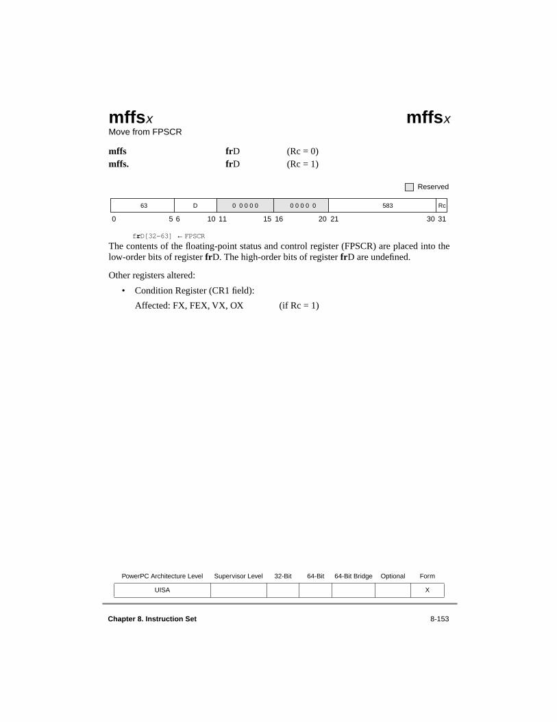
Chapter 8. Instruction Set 8-153
mffsx mffsx Move from FPSCR
mffs frD (Rc = 0)mffs. frD (Rc = 1)
frD[32-63] ← FPSCRThe contents of the floating-point status and control register (FPSCR) are placed into thelow-order bits of register frD. The high-order bits of register frD are undefined.
Other registers altered:
• Condition Register (CR1 field):
Affected: FX, FEX, VX, OX (if Rc = 1)
PowerPC Architecture Level Supervisor Level 32-Bit 64-Bit 64-Bit Bridge Optional Form
UISA X
0 5 6 10 11 15 16 20 21 30 31
Reserved
0 0 0 0 0 583 Rc63 D 0 0 0 0 0

8-154 PowerPC Microprocessor Family: The Programming Environments, Rev. 1
mfmsr mfmsr Move from Machine State Register
mfmsr rD
rD ← MSRThe contents of the MSR are placed into rD.
This is a supervisor-level instruction.
Other registers altered:
• None
PowerPC Architecture Level Supervisor Level 32-Bit 64-Bit 64-Bit Bridge Optional Form
OEA √ X
0 5 6 10 11 15 16 20 21 30 31
Reserved
0 0 0 0 0 83 031 D 0 0 0 0 0
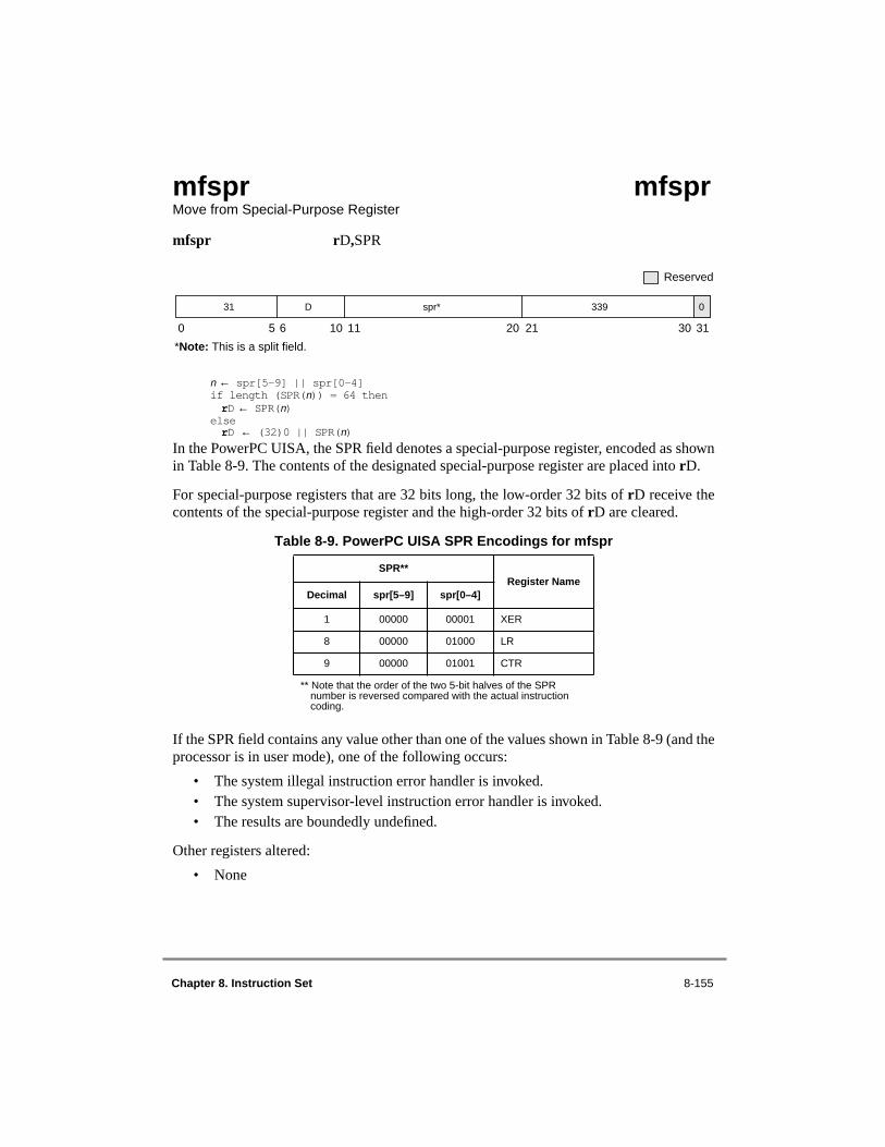
Chapter 8. Instruction Set 8-155
mfspr mfspr Move from Special-Purpose Register
mfspr rD,SPR
n ← spr[5–9] || spr[0–4]if length (SPR(n)) = 64 thenrD ← SPR(n)
elserD ← (32)0 || SPR(n)
In the PowerPC UISA, the SPR field denotes a special-purpose register, encoded as shownin Table 8-9. The contents of the designated special-purpose register are placed into rD.
For special-purpose registers that are 32 bits long, the low-order 32 bits of rD receive thecontents of the special-purpose register and the high-order 32 bits of rD are cleared.
If the SPR field contains any value other than one of the values shown in Table 8-9 (and theprocessor is in user mode), one of the following occurs:
• The system illegal instruction error handler is invoked.• The system supervisor-level instruction error handler is invoked.• The results are boundedly undefined.
Other registers altered:
• None
Table 8-9. PowerPC UISA SPR Encodings for mfspr
SPR**Register Name
Decimal spr[5–9] spr[0–4]
1 00000 00001 XER
8 00000 01000 LR
9 00000 01001 CTR
** Note that the order of the two 5-bit halves of the SPR number is reversed compared with the actual instruction coding.
0 5 6 10 11 20 21 30 31
Reserved
spr* 339 031 D
*Note: This is a split field.

8-156 PowerPC Microprocessor Family: The Programming Environments, Rev. 1
Simplified mnemonics:
mfxer rD equivalent to mfspr rD,1mflr rD equivalent to mfspr rD,8mfctr rD equivalent to mfspr rD,9
In the PowerPC OEA, the SPR field denotes a special-purpose register, encoded as shownin Table 8-10. The contents of the designated SPR are placed into rD. For SPRs that are 32bits long, the low-order 32 bits of rD receive the contents of the SPR and the high-order 32bits of rD are cleared.
SPR[0] = 1 if and only if reading the register is supervisor-level. Execution of thisinstruction specifying a defined and supervisor-level register when MSR[PR] = 1 will resultin a privileged instruction type program exception.
If MSR[PR] = 1, the only effect of executing an instruction with an SPR number that is notshown in Table 8-10 and has SPR[0] = 1 is to cause a supervisor-level instruction typeprogram exception or an illegal instruction type program exception. For all other cases,MSR[PR] = 0 or SPR[0] = 0. If the SPR field contains any value that is not shown inTable 8-10, either an illegal instruction type program exception occurs or the results areboundedly undefined.
Other registers altered:
• None
Table 8-10. PowerPC OEA SPR Encodings for mfspr
SPR1
Register Name
AccessDecimal spr[5–9] spr[0–4]
1 00000 00001 XER User
8 00000 01000 LR User
9 00000 01001 CTR User
18 00000 10010 DSISR Supervisor
19 00000 10011 DAR Supervisor
22 00000 10110 DEC Supervisor
25 00000 11001 SDR1 Supervisor
26 00000 11010 SRR0 Supervisor
27 00000 11011 SRR1 Supervisor
272 01000 10000 SPRG0 Supervisor
273 01000 10001 SPRG1 Supervisor
274 01000 10010 SPRG2 Supervisor
275 01000 10011 SPRG3 Supervisor

Chapter 8. Instruction Set 8-157
280 01000 11000 ASR2 Supervisor
282 01000 11010 EAR Supervisor
287 01000 11111 PVR Supervisor
528 10000 10000 IBAT0U Supervisor
529 10000 10001 IBAT0L Supervisor
530 10000 10010 IBAT1U Supervisor
531 10000 10011 IBAT1L Supervisor
532 10000 10100 IBAT2U Supervisor
533 10000 10101 IBAT2L Supervisor
534 10000 10110 IBAT3U Supervisor
535 10000 10111 IBAT3L Supervisor
536 10000 11000 DBAT0U Supervisor
537 10000 11001 DBAT0L Supervisor
538 10000 11010 DBAT1U Supervisor
539 10000 11011 DBAT1L Supervisor
540 10000 11100 DBAT2U Supervisor
541 10000 11101 DBAT2L Supervisor
542 10000 11110 DBAT3U Supervisor
543 10000 11111 DBAT3L Supervisor
1013 11111 10101 DABR Supervisor
1Note that the order of the two 5-bit halves of the SPR number is reversed compared with actual instruction coding.
For mtspr and mfspr instructions, the SPR number coded in assembly language does not appear directly as a 10-bit binary number in the instruction. The number coded is split into two 5-bit halves that are reversed in the instruction, with the high-order five bits appearing in bits 16–20 of the instruction and the low-order five bits in bits 11–15.
264-bit implementations only.
PowerPC Architecture Level Supervisor Level 32-Bit 64-Bit 64-Bit Bridge Optional Form
UISA/OEA √* XFX
* Note that mfspr is supervisor-level only if SPR[0] = 1.
Table 8-10. PowerPC OEA SPR Encodings for mfspr (Continued)
SPR1
Register Name
AccessDecimal spr[5–9] spr[0–4]
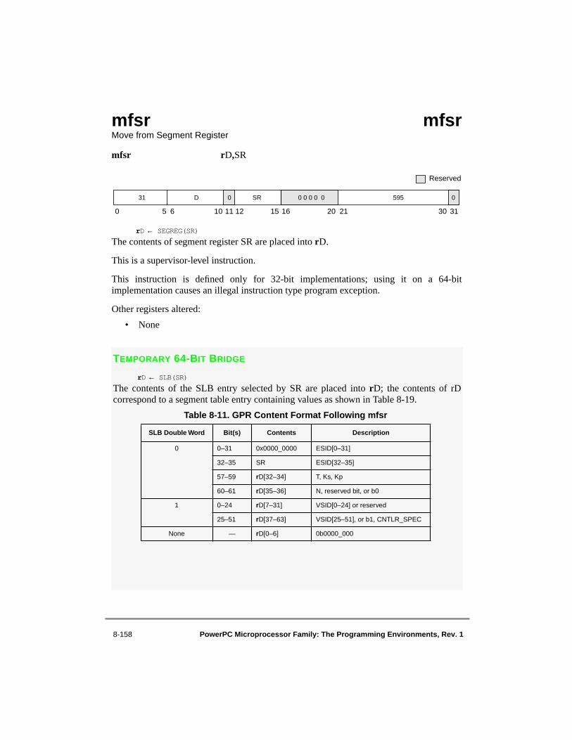
8-158 PowerPC Microprocessor Family: The Programming Environments, Rev. 1
mfsr mfsr Move from Segment Register
mfsr rD,SR
rD ← SEGREG(SR)
The contents of segment register SR are placed into rD.
This is a supervisor-level instruction.
This instruction is defined only for 32-bit implementations; using it on a 64-bitimplementation causes an illegal instruction type program exception.
Other registers altered:
• None
TEMPORARY 64-BIT BRIDGE
rD ← SLB(SR)
The contents of the SLB entry selected by SR are placed into rD; the contents of rDcorrespond to a segment table entry containing values as shown in Table 8-19.
0 5 6 10 11 12 15 16 20 21 30 31
Reserved
0 0 0 0 0 595 031 D 0 SR
Table 8-11. GPR Content Format Following mfsr
SLB Double Word Bit(s) Contents Description
0 0–31 0x0000_0000 ESID[0–31]
32–35 SR ESID[32–35]
57–59 rD[32–34] T, Ks, Kp
60–61 rD[35–36] N, reserved bit, or b0
1 0–24 rD[7–31] VSID[0–24] or reserved
25–51 rD[37–63] VSID[25–51], or b1, CNTLR_SPEC
None — rD[0–6] 0b0000_000

Chapter 8. Instruction Set 8-159
If the SLB entry selected by SR was not created by an mtsr, mtsrd, or mtsrdin instruction,the contents of rD are undefined.
This is a supervisor-level instruction.
Other registers altered:
• None
PowerPC Architecture Level Supervisor Level 32-Bit 64-Bit 64-Bit Bridge Optional Form
OEA √ √ √ X

8-160 PowerPC Microprocessor Family: The Programming Environments, Rev. 1
mfsrin mfsrin Move from Segment Register Indirect
mfsrin rD,rB
rD ← SEGREG(rB[0–3])
The contents of the segment register selected by bits 0–3 of rB are copied into rD.
This is a supervisor-level instruction.
This instruction is defined only for 32-bit implementations. Using it on a 64-bitimplementation causes an illegal instruction type program exception.
Note that the rA field is not defined for the mfsrin instruction in the PowerPC architecture.However, mfsrin performs the same function in the PowerPC architecture as does the mfsriinstruction in the POWER architecture (if rA = 0).
Other registers altered:
• None
TEMPORARY 64-BIT BRIDGE
rD ← SLB(rB[32-35])
The contents of the SLB entry selected by rB[32–35] are placed into rD; the contents ofrD correspond to a segment table entry containing values as shown in Table 8-19:
0 5 6 10 11 15 16 20 21 30 31
Reserved
B 659 031 D 0 0 0 0 0
Table 8-12. GPR Content Format Following mfsrin
Doubleword Bit(s) Contents Description
0 0-31 0x0000_0000 ESID[0–31]
32-35 rB[32–35] ESID[32–35]
57-59 rD[32–34] T, Ks, Kp
60-61 rD[35–36] N, reserved bit, or b0
1 0-24 rD[7–31] VSID[0–24] or reserved
25-51 rD[37–63] VSID[25–51], or b1, CNTLR_SPEC
none 70 rD[0–6] 0b0000_000

Chapter 8. Instruction Set 8-161
If the SLB entry selected by rB[32–35] was not created by an mtsr, mtsrd, or mtsrdininstruction, the contents of rD are undefined.
This is a supervisor-level instruction.
Other registers altered:
• None
PowerPC Architecture Level Supervisor Level 32-Bit 64-Bit 64-Bit Bridge Optional Form
OEA √ √ √ X

8-162 PowerPC Microprocessor Family: The Programming Environments, Rev. 1
mftb mftb Move from Time Base
mftb rD,TBR
n ← tbr[5–9] || tbr[0–4]if n = 268 thenif (64-bit implementation) thenrD ← TB
elserD ← TBL
else if n = 269 thenif (64-bit implementation) thenrD ← (32)0 || TBU
elserD ← TBU
When reading the time base lower (TBL) on a 64-bit implementation, the contents of theentire time base (TBU || TBL) is copied into rD. Note that when reading time base upper(TBU) on a 64-bit implementation the high-order 32 bits of rD are cleared. The TBR fielddenotes either the TBL or TBU, encoded as shown in Table 8-13.
If the TBR field contains any value other than one of the values shown in Table 8-13, thenone of the following occurs:
• The system illegal instruction error handler is invoked.• The system supervisor-level instruction error handler is invoked.• The results are boundedly undefined.
It is important to note that some implementations may implement mftb and mfspridentically, therefore, a TBR number must not match an SPR number.
For more information on the time base refer to Section 2.2, “PowerPC VEA RegisterSet—Time Base.”
Table 8-13. TBR Encodings for mftb
TBR*Register
NameAccess
Decimal tbr[5–9] tbr[0–4]
268 01000 01100 TBL User
269 01000 01101 TBU User
*Note that the order of the two 5-bit halves of the TBR number is reversed.
0 5 6 10 11 20 21 30 31
Reserved
31 D tbr* 371 0
*Note: This is a split field.
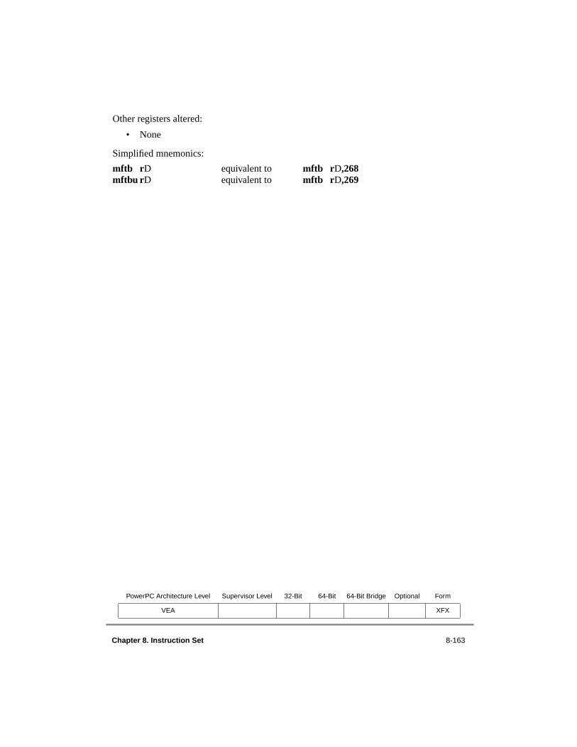
Chapter 8. Instruction Set 8-163
Other registers altered:
• None
Simplified mnemonics:
mftb rD equivalent to mftb rD,268mftbu rD equivalent to mftb rD,269
PowerPC Architecture Level Supervisor Level 32-Bit 64-Bit 64-Bit Bridge Optional Form
VEA XFX

8-164 PowerPC Microprocessor Family: The Programming Environments, Rev. 1
mtcrf mtcrf Move to Condition Register Fields
mtcrf CRM,rS
mask ← (4)(CRM[0]) || (4)(CRM[1]) ||... (4)(CRM[7])CR ← (rS[32–63] & mask) | (CR & ¬ mask)
The contents of the low-order 32 bits of rS are placed into the condition register undercontrol of the field mask specified by CRM. The field mask identifies the 4-bit fieldsaffected. Let i be an integer in the range 0–7. If CRM(i) = 1, CR field i (CR bits 4 ∗ i through4 ∗ i + 3) is set to the contents of the corresponding field of the low-order 32 bits of rS.
Note that updating a subset of the eight fields of the condition register may havesubstantially poorer performance on some implementations than updating all of the fields.
Other registers altered:
• CR fields selected by mask
Simplified mnemonics:
mtcr rS equivalent to mtcrf 0xFF,rS
PowerPC Architecture Level Supervisor Level 32-Bit 64-Bit 64-Bit Bridge Optional Form
UISA XFX
0 5 6 10 11 12 19 20 21 30 31
Reserved
CRM 0 144 031 S 0
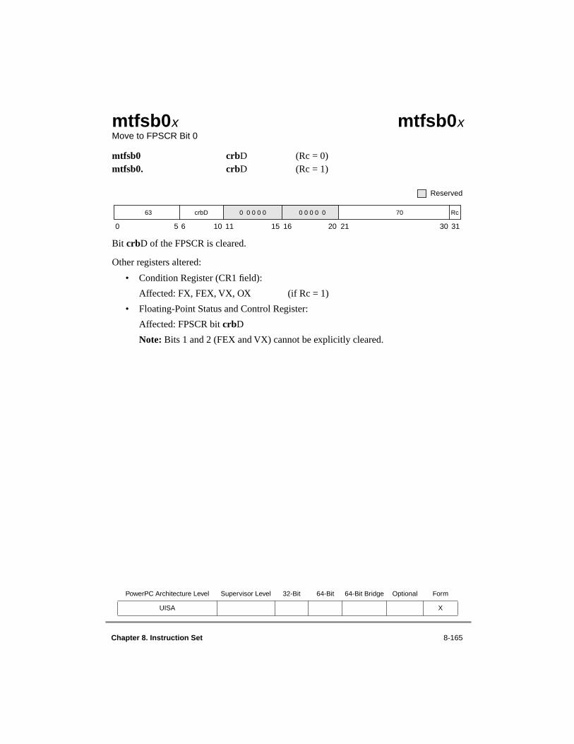
Chapter 8. Instruction Set 8-165
mtfsb0x mtfsb0xMove to FPSCR Bit 0
mtfsb0 crbD (Rc = 0)mtfsb0. crbD (Rc = 1)
Bit crbD of the FPSCR is cleared.
Other registers altered:
• Condition Register (CR1 field):
Affected: FX, FEX, VX, OX (if Rc = 1)
• Floating-Point Status and Control Register:
Affected: FPSCR bit crbD
Note: Bits 1 and 2 (FEX and VX) cannot be explicitly cleared.
PowerPC Architecture Level Supervisor Level 32-Bit 64-Bit 64-Bit Bridge Optional Form
UISA X
0 5 6 10 11 15 16 20 21 30 31
Reserved
0 0 0 0 0 70 Rc63 crbD 0 0 0 0 0

8-166 PowerPC Microprocessor Family: The Programming Environments, Rev. 1
mtfsb1x mtfsb1x Move to FPSCR Bit 1
mtfsb1 crbD (Rc = 0)mtfsb1. crbD (Rc = 1)
Bit crbD of the FPSCR is set.
Other registers altered:
• Condition Register (CR1 field):
Affected: FX, FEX, VX, OX (if Rc = 1)
• Floating-Point Status and Control Register:
Affected: FPSCR bit crbD and FX
Note: Bits 1 and 2 (FEX and VX) cannot be explicitly set.
PowerPC Architecture Level Supervisor Level 32-Bit 64-Bit 64-Bit Bridge Optional Form
UISA X
0 5 6 10 11 15 16 20 21 30 31
Reserved
0 0 0 0 0 38 Rc63 crbD 0 0 0 0 0

Chapter 8. Instruction Set 8-167
mtfsfx mtfsfxMove to FPSCR Fields
mtfsf FM,frB (Rc = 0)mtfsf. FM,frB (Rc = 1)
The low-order 32 bits of frB are placed into the FPSCR under control of the field maskspecified by FM. The field mask identifies the 4-bit fields affected. Let i be an integer in therange 0–7. If FM[i] = 1, FPSCR field i (FPSCR bits 4 * i through 4 * i + 3) is set to thecontents of the corresponding field of the low-order 32 bits of register frB.
FPSCR[FX] is altered only if FM[0] = 1.
Updating fewer than all eight fields of the FPSCR may have substantially poorerperformance on some implementations than updating all the fields.
When FPSCR[0–3] is specified, bits 0 (FX) and 3 (OX) are set to the values of frB[32] andfrB[35] (that is, even if this instruction causes OX to change from 0 to 1, FX is set fromfrB[32] and not by the usual rule that FX is set when an exception bit changes from 0 to 1).Bits 1 and 2 (FEX and VX) are set according to the usual rule and not from frB[33–34].
Other registers altered:
• Condition Register (CR1 field):
Affected: FX, FEX, VX, OX (if Rc = 1)
• Floating-Point Status and Control Register:
Affected: FPSCR fields selected by mask
PowerPC Architecture Level Supervisor Level 32-Bit 64-Bit 64-Bit Bridge Optional Form
UISA XFL
0 5 6 7 14 15 16 20 21 30 31
Reserved
63 0 FM 0 B 711 Rc
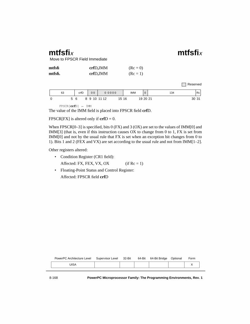
8-168 PowerPC Microprocessor Family: The Programming Environments, Rev. 1
mtfsfix mtfsfix
Move to FPSCR Field Immediate
mtfsfi crfD,IMM (Rc = 0)mtfsfi. crfD,IMM (Rc = 1)
FPSCR[crfD] ← IMM
The value of the IMM field is placed into FPSCR field crfD.
FPSCR[FX] is altered only if crfD = 0.
When FPSCR[0–3] is specified, bits 0 (FX) and 3 (OX) are set to the values of IMM[0] andIMM[3] (that is, even if this instruction causes OX to change from 0 to 1, FX is set fromIMM[0] and not by the usual rule that FX is set when an exception bit changes from 0 to1). Bits 1 and 2 (FEX and VX) are set according to the usual rule and not from IMM[1–2].
Other registers altered:
• Condition Register (CR1 field):
Affected: FX, FEX, VX, OX (if Rc = 1)
• Floating-Point Status and Control Register:
Affected: FPSCR field crfD
PowerPC Architecture Level Supervisor Level 32-Bit 64-Bit 64-Bit Bridge Optional Form
UISA X
0 5 6 8 9 10 11 12 15 16 19 20 21 30 31
Reserved
63 crfD 0 0 0 0 0 0 0 IMM 0 134 Rc

Chapter 8. Instruction Set 8-169
mtmsr mtmsr Move to Machine State Register
mtmsr rS
MSR ← (rS)
The contents of rS are placed into the MSR.
This is a supervisor-level instruction. It is also an execution synchronizing instructionexcept with respect to alterations to the POW and LE bits. Refer to Section 2.3.18,“Synchronization Requirements for Special Registers and for Lookaside Buffers,” for moreinformation.
In addition, alterations to the MSR[EE] and MSR[RI] bits are effective as soon as theinstruction completes. Thus if MSR[EE] = 0 and an external or decrementer exception ispending, executing an mtmsr instruction that sets MSR[EE] = 1 will cause the external ordecrementer exception to be taken before the next instruction is executed, if no higherpriority exception exists.
This instruction is defined only for 32-bit implementations. Using it on a 64-bitimplementation causes an illegal instruction type program exception.
Other registers altered:
• MSR
TEMPORARY 64-BIT BRIDGE
The mtmsr instruction may optionally be provided by a 64-bit implementation. Theoperation of the mtmsr instruction in a 64-bit implementation is identical to operation ina 32-bit implementation, except as described below:
• Bits 32–63 of rS are placed into the corresponding bits of the MSR. The high-order 32 bits of the MSR are unchanged.
Note that there is no need for an optional version of the mfmsr instruction, as the existinginstruction copies the entire contents of the MSR to the selected GPR.
0 5 6 10 11 15 16 20 21 30 31
Reserved
0 0 0 0 0 146 031 S 0 0 0 0 0

8-170 PowerPC Microprocessor Family: The Programming Environments, Rev. 1
When the optional mtmsr instruction is provided in a 64-bit implementation, the optionalrfi instruction is also provided. Refer to the rfi instruction description for additional detailabout the operation of the rfi instruction in 64-bit implementations.
PowerPC Architecture Level Supervisor Level 32-Bit 64-Bit 64-Bit Bridge Optional Form
OEA √ √ √ X
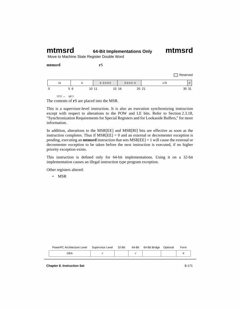
Chapter 8. Instruction Set 8-171
mtmsrd 64-Bit Implementations Only mtmsrd Move to Machine State Register Double Word
mtmsrd rS
MSR ← (rS)
The contents of rS are placed into the MSR.
This is a supervisor-level instruction. It is also an execution synchronizing instructionexcept with respect to alterations to the POW and LE bits. Refer to Section 2.3.18,“Synchronization Requirements for Special Registers and for Lookaside Buffers,” for moreinformation.
In addition, alterations to the MSR[EE] and MSR[RI] bits are effective as soon as theinstruction completes. Thus if MSR[EE] = 0 and an external or decrementer exception ispending, executing an mtmsrd instruction that sets MSR[EE] = 1 will cause the external ordecrementer exception to be taken before the next instruction is executed, if no higherpriority exception exists.
This instruction is defined only for 64-bit implementations. Using it on a 32-bitimplementation causes an illegal instruction type program exception.
Other registers altered:
• MSR
PowerPC Architecture Level Supervisor Level 32-Bit 64-Bit 64-Bit Bridge Optional Form
OEA √ √ X
0 5 6 10 11 15 16 20 21 30 31
Reserved
0 0 0 0 0 178 031 S 0 0 0 0 0

8-172 PowerPC Microprocessor Family: The Programming Environments, Rev. 1
mtspr mtsprMove to Special-Purpose Register
mtspr SPR,rS
n ← spr[5–9] || spr[0–4]if length (SPR(n)) = 64 thenSPR(n) ← (rS)
elseSPR(n) ← rS[32–63]
In the PowerPC UISA, the SPR field denotes a special-purpose register, encoded as shownin Table 8-14. The contents of rS are placed into the designated special-purpose register.For special-purpose registers that are 32 bits long, the low-order 32 bits of rS are placedinto the SPR.
If the SPR field contains any value other than one of the values shown in Table 8-14, andthe processor is operating in user mode, one of the following occurs:
• The system illegal instruction error handler is invoked.• The system supervisor instruction error handler is invoked.• The results are boundedly undefined.
Other registers altered:
• See Table 8-14.
Simplified mnemonics:
mtxer rD equivalent to mtspr 1,rDmtlr rD equivalent to mtspr 8,rDmtctr rD equivalent to mtspr 9,rD
Table 8-14. PowerPC UISA SPR Encodings for mtspr
SPR**Register Name
Decimal spr[5–9] spr[0–4]
1 00000 00001 XER
8 00000 01000 LR
9 00000 01001 CTR
** Note that the order of the two 5-bit halves of the SPR number is reversed compared with actual instruction coding.
0 5 6 10 11 20 21 30 31
Reserved
spr* 467 031 S
*Note: This is a split field.

Chapter 8. Instruction Set 8-173
In the PowerPC OEA, the SPR field denotes a special-purpose register, encoded as shownin Table 8-15. The contents of rS are placed into the designated special-purpose register.For special-purpose registers that are 32 bits long, the low-order 32 bits of rS are placedinto the SPR.
For this instruction, SPRs TBL and TBU are treated as separate 32-bit registers; setting oneleaves the other unaltered.
The value of SPR[0] = 1 if and only if writing the register is a supervisor-level operation.Execution of this instruction specifying a defined and supervisor-level register whenMSR[PR] = 1 results in a privileged instruction type program exception.
If MSR[PR] = 1 then the only effect of executing an instruction with an SPR number thatis not shown in Table 8-15 and has SPR[0] = 1 is to cause a privileged instruction typeprogram exception or an illegal instruction type program exception. For all other cases,MSR[PR] = 0 or SPR[0] = 0, if the SPR field contains any value that is not shown inTable 8-15, either an illegal instruction type program exception occurs or the results areboundedly undefined.
Other registers altered:
• See Table 8-15.
Table 8-15. PowerPC OEA SPR Encodings for mtspr
SPR1
Register Name
AccessDecimal spr[5–9] spr[0–4]
1 00000 00001 XER User
8 00000 01000 LR User
9 00000 01001 CTR User
18 00000 10010 DSISR Supervisor
19 00000 10011 DAR Supervisor
22 00000 10110 DEC Supervisor
25 00000 11001 SDR1 Supervisor
26 00000 11010 SRR0 Supervisor
27 00000 11011 SRR1 Supervisor
272 01000 10000 SPRG0 Supervisor
273 01000 10001 SPRG1 Supervisor
274 01000 10010 SPRG2 Supervisor
275 01000 10011 SPRG3 Supervisor
280 01000 11000 ASR2 Supervisor
282 01000 11010 EAR Supervisor

8-174 PowerPC Microprocessor Family: The Programming Environments, Rev. 1
284 01000 11100 TBL Supervisor
285 01000 11101 TBU Supervisor
528 10000 10000 IBAT0U Supervisor
529 10000 10001 IBAT0L Supervisor
530 10000 10010 IBAT1U Supervisor
531 10000 10011 IBAT1L Supervisor
532 10000 10100 IBAT2U Supervisor
533 10000 10101 IBAT2L Supervisor
534 10000 10110 IBAT3U Supervisor
535 10000 10111 IBAT3L Supervisor
536 10000 11000 DBAT0U Supervisor
537 10000 11001 DBAT0L Supervisor
538 10000 11010 DBAT1U Supervisor
539 10000 11011 DBAT1L Supervisor
540 10000 11100 DBAT2U Supervisor
541 10000 11101 DBAT2L Supervisor
542 10000 11110 DBAT3U Supervisor
543 10000 11111 DBAT3L Supervisor
1013 11111 10101 DABR Supervisor
1Note that the order of the two 5-bit halves of the SPR number is reversed. For mtspr and mfspr instructions, the SPR number coded in assembly language does not appear directly as a 10-bit binary number in the instruction. The number coded is split into two 5-bit halves that are reversed in the instruction, with the high-order five bits appearing in bits 16–20 of the instruction and the low-order five bits in bits 11–15.
264-bit implementations only.
PowerPC Architecture Level Supervisor Level 32-Bit 64-Bit 64-Bit Bridge Optional Form
UISA/OEA √* XFX
* Note that mtspr is supervisor-level only if SPR[0] = 1.
Table 8-15. PowerPC OEA SPR Encodings for mtspr (Continued)
SPR1
Register Name
AccessDecimal spr[5–9] spr[0–4]
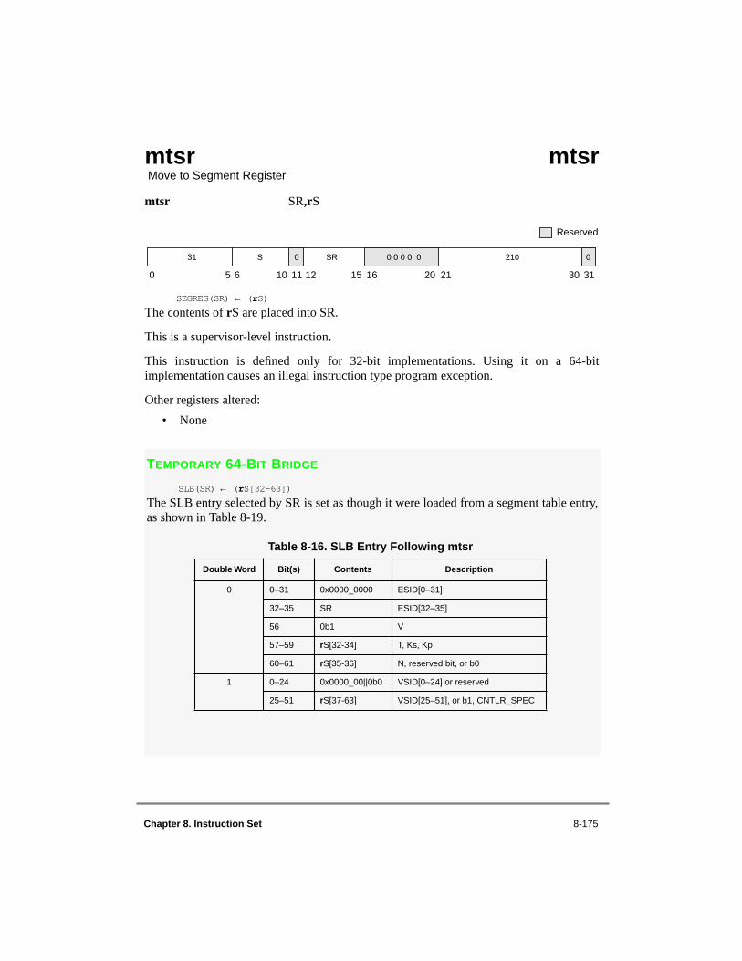
Chapter 8. Instruction Set 8-175
mtsr mtsr Move to Segment Register
mtsr SR,rS
SEGREG(SR) ← (rS)
The contents of rS are placed into SR.
This is a supervisor-level instruction.
This instruction is defined only for 32-bit implementations. Using it on a 64-bitimplementation causes an illegal instruction type program exception.
Other registers altered:
• None
TEMPORARY 64-BIT BRIDGE
SLB(SR) ← (rS[32-63])
The SLB entry selected by SR is set as though it were loaded from a segment table entry,as shown in Table 8-19.
0 5 6 10 11 12 15 16 20 21 30 31
Reserved
0 0 0 0 0 210 031 S 0 SR
Table 8-16. SLB Entry Following mtsr
Double Word Bit(s) Contents Description
0 0–31 0x0000_0000 ESID[0–31]
32–35 SR ESID[32–35]
56 0b1 V
57–59 rS[32-34] T, Ks, Kp
60–61 rS[35-36] N, reserved bit, or b0
1 0–24 0x0000_00||0b0 VSID[0–24] or reserved
25–51 rS[37-63] VSID[25–51], or b1, CNTLR_SPEC

8-176 PowerPC Microprocessor Family: The Programming Environments, Rev. 1
This is a supervisor-level instruction.
Note that when creating an ordinary segment (T = 0) using the mtsr instruction, rS[36–39]should be set to 0x0, as these bits correspond to the reserved bits in the T = 0 format for asegment register.
Other registers altered:
• None
PowerPC Architecture Level Supervisor Level 32-Bit 64-Bit 64-Bit Bridge Optional Form
OEA √ √ √ X

Chapter 8. Instruction Set 8-177
TEMPORARY 64-BIT BRIDGE
mtsrd 64-Bit Implementations Only mtsrd Move to Segment Register Double Word
mtsrd SR,rS
SLB(SR) ← (rS)
The contents of rS are placed into the SLB selected by SR. The SLB entry is set as thoughit were loaded from an STE, as shown in Table 8-19.
This is a supervisor-level instruction.
This instruction is optional, and is defined only for 64-bit implementations. If the mtsrdinstruction is implemented, the mtsrdin instruction will also be implemented. Using it ona 32-bit implementation causes an illegal instruction type program exception.
Other registers altered:
• None
0 5 6 10 11 12 15 16 20 21 30 31
Reserved
0 0 0 0 0 82 031 S 0 SR
Table 8-17. SLB Entry Following mtsrd
Double Word Bit(s) Contents Description
0 0–31 0x0000_0000 ESID[0–31]
32–35 SR ESID[32–35]
56 0b1 V
57–59 rS[32–34] T, Ks, Kp
60–61 rS[35–36] N, reserved bit, or b0
1 0–24 rS[7–31] VSID[0–24] or reserved
25–51 rS[37–63] VSID[25–51], or b1, CNTLR_SPEC
PowerPC Architecture Level Supervisor Level 32-Bit 64-Bit 64-Bit Bridge Optional Form
OEA √ √ √ √ X

8-178 PowerPC Microprocessor Family: The Programming Environments, Rev. 1
TEMPORARY 64-BIT BRIDGE
mtsrdin 64-Bit Implementations Only mtsrdin Move to Segment Register Double Word Indirect
mtsrdin rS,rB
SLB(rB[32-35]) ← (rS)
The contents of rS are copied to the SLB selected by bits 32–35 of rB. The SLB entry isset as though it were loaded from an STE, as shown in Table 8-18.
This is a supervisor-level instruction.
This instruction is optional, and defined only for 64-bit implementations. If the mtsrdininstruction is implemented, the mtsrd instruction will also be implemented. Using it on a32-bit implementation causes an illegal instruction exception.
Other registers altered:
• None
0 5 6 10 11 15 16 20 21 30 31
Reserved
B 114 031 S 0 0 0 0 0
Table 8-18. SLB Entry following mtsrdin
Double Word Bit(s) Contents Description
0 0–31 0x0000_0000 ESID[0–31]
32–35 rB[32–35] ESID[32–35]
56 0b1 V
57–59 rS[32–34] T, Ks, Kp
60–61 rS[35–36] N, reserved bit, or b0
1 0–24 rS[7–31] VSID[0-24] or reserved
25–51 rS[37–63] VSID[25–51], or b1, CNTLR_SPEC
PowerPC Architecture Level Supervisor Level 32-Bit 64-Bit 64-Bit Bridge Optional Form
OEA √ √ √ √ X

Chapter 8. Instruction Set 8-179
mtsrin mtsrin Move to Segment Register Indirect
mtsrin rS,rB
[POWER mnemonic: mtsri]
SEGREG(rB[0–3]) ← (rS)
The contents of rS are copied to the segment register selected by bits 0–3 of rB.
This is a supervisor-level instruction.
This instruction is defined only for 32-bit implementations. Using it on a 64-bitimplementation causes an illegal instruction type program exception.
Note that the PowerPC architecture does not define the rA field for the mtsrin instruction.However, mtsrin performs the same function in the PowerPC architecture as does the mtsriinstruction in the POWER architecture (if rA = 0).
Other registers altered:
• None
0 5 6 10 11 15 16 20 21 30 31
Reserved
B 242 031 S 0 0 0 0 0

8-180 PowerPC Microprocessor Family: The Programming Environments, Rev. 1
TEMPORARY 64-BIT BRIDGE
SLB(rB[32-35]) ← (rS[32-63])
The SLB entry selected by bits 32-35 of rB is set as though it were loaded from a segmenttable entry, as shown in Table 8-19.
This is a supervisor-level instruction.
Note that when creating an ordinary segment (T = 0) using the mtsrin instruction,rS[36–39] should be set to 0x0, as these bits correspond to the reserved bits in the T = 0format for a segment register.
Other registers altered:
• None
PowerPC Architecture Level Supervisor Level 32-Bit 64-Bit 64-Bit Bridge Optional Form
OEA √ √ √ X
Table 8-19. SLB Entry Following mtsrin
Double Word Bit(s) Contents Description
0 0–31 0x0000_0000 ESID[0–31]
32–35 rB[32–35] ESID[32–35]
56 0b1 V
57–59 rS[32–34] T, Ks, Kp
60–61 rS[35–36] N, reserved bit, or b0
1 0–24 0x0000_00||0b0 VSID[0–24] or reserved
25–51 rS[37–63] VSID[25–51], or b1, CNTLR_SPEC
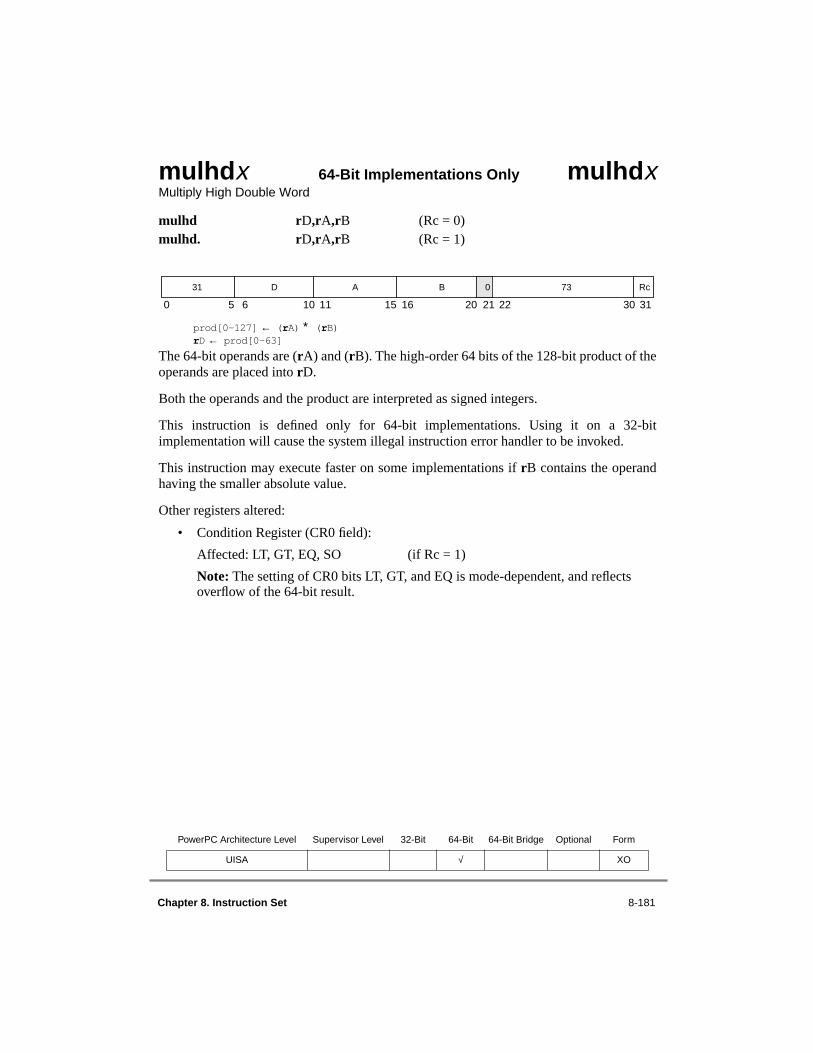
Chapter 8. Instruction Set 8-181
mulhdx 64-Bit Implementations Only mulhdxMultiply High Double Word
mulhd rD,rA,rB (Rc = 0)mulhd. rD,rA,rB (Rc = 1)
prod[0–127] ← (rA) ∗ (rB)rD ← prod[0–63]
The 64-bit operands are (rA) and (rB). The high-order 64 bits of the 128-bit product of theoperands are placed into rD.
Both the operands and the product are interpreted as signed integers.
This instruction is defined only for 64-bit implementations. Using it on a 32-bitimplementation will cause the system illegal instruction error handler to be invoked.
This instruction may execute faster on some implementations if rB contains the operandhaving the smaller absolute value.
Other registers altered:
• Condition Register (CR0 field):
Affected: LT, GT, EQ, SO (if Rc = 1)
Note: The setting of CR0 bits LT, GT, and EQ is mode-dependent, and reflects overflow of the 64-bit result.
PowerPC Architecture Level Supervisor Level 32-Bit 64-Bit 64-Bit Bridge Optional Form
UISA √ XO
0 5 6 10 11 15 16 20 21 22 30 31
31 D A B 0 73 Rc
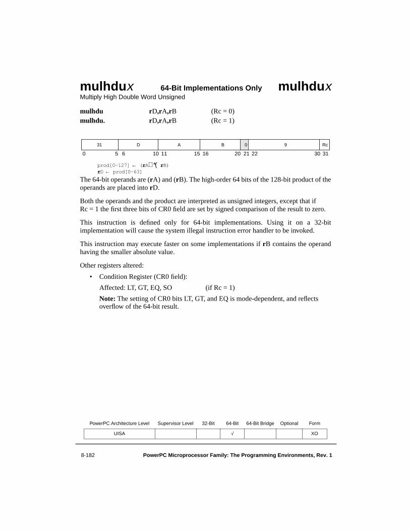
8-182 PowerPC Microprocessor Family: The Programming Environments, Rev. 1
mulhdux 64-Bit Implementations Only mulhduxMultiply High Double Word Unsigned
mulhdu rD,rA,rB (Rc = 0)mulhdu. rD,rA,rB (Rc = 1)
prod[0–127] ← (rA) ∗ ( rB)rD ← prod[0–63]
The 64-bit operands are (rA) and (rB). The high-order 64 bits of the 128-bit product of theoperands are placed into rD.
Both the operands and the product are interpreted as unsigned integers, except that if Rc = 1 the first three bits of CR0 field are set by signed comparison of the result to zero.
This instruction is defined only for 64-bit implementations. Using it on a 32-bitimplementation will cause the system illegal instruction error handler to be invoked.
This instruction may execute faster on some implementations if rB contains the operandhaving the smaller absolute value.
Other registers altered:
• Condition Register (CR0 field):
Affected: LT, GT, EQ, SO (if Rc = 1)
Note: The setting of CR0 bits LT, GT, and EQ is mode-dependent, and reflects overflow of the 64-bit result.
PowerPC Architecture Level Supervisor Level 32-Bit 64-Bit 64-Bit Bridge Optional Form
UISA √ XO
0 5 6 10 11 15 16 20 21 22 30 31
31 D A B 0 9 Rc
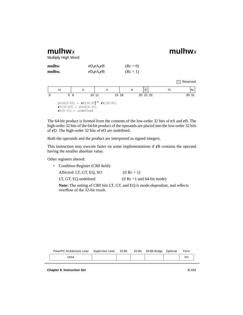
Chapter 8. Instruction Set 8-183
mulhwx mulhwx Multiply High Word
mulhw rD,rA,rB (Rc = 0)mulhw. rD,rA,rB (Rc = 1)
prod[0–63] ← rA[32–63] ∗ rB[32–63]rD[32–63] ← prod[0–31]rD[0–31] ← undefined
The 64-bit product is formed from the contents of the low-order 32 bits of rA and rB. Thehigh-order 32 bits of the 64-bit product of the operands are placed into the low-order 32 bitsof rD. The high-order 32 bits of rD are undefined.
Both the operands and the product are interpreted as signed integers.
This instruction may execute faster on some implementations if rB contains the operandhaving the smaller absolute value.
Other registers altered:
• Condition Register (CR0 field):
Affected: LT, GT, EQ, SO (if Rc = 1)
LT, GT, EQ undefined (if Rc =1 and 64-bit mode)
Note: The setting of CR0 bits LT, GT, and EQ is mode-dependent, and reflects overflow of the 32-bit result.
PowerPC Architecture Level Supervisor Level 32-Bit 64-Bit 64-Bit Bridge Optional Form
UISA XO
Reserved
0 5 6 10 11 15 16 20 21 22 30 31
31 D A B 0 75 Rc

8-184 PowerPC Microprocessor Family: The Programming Environments, Rev. 1
mulhwux mulhwux Multiply High Word Unsigned
mulhwu rD,rA,rB (Rc = 0)mulhwu. rD,rA,rB (Rc = 1)
prod[0–63] ← rA[32–63] ∗ rB[32–63]rD[32–63] ← prod[0–31]rD[0–31] ← undefined
The 32-bit operands are the contents of the low-order 32 bits of rA and rB. The high-order32 bits of the 64-bit product of the operands are placed into the low-order 32 bits of rD. Thehigh-order 32 bits of rD are undefined.
Both the operands and the product are interpreted as unsigned integers, except that if Rc = 1 the first three bits of CR0 field are set by signed comparison of the result to zero.
This instruction may execute faster on some implementations if rB contains the operandhaving the smaller absolute value.
Other registers altered:
• Condition Register (CR0 field):
Affected: LT, GT, EQ, SO (if Rc = 1)
LT, GT, EQ undefined (if Rc =1 and 64-bit mode)
Note: The setting of CR0 bits LT, GT, and EQ is mode-dependent, and reflects overflow of the 32-bit result.
PowerPC Architecture Level Supervisor Level 32-Bit 64-Bit 64-Bit Bridge Optional Form
UISA XO
Reserved
0 5 6 10 11 15 16 20 21 22 30 31
31 D A B 0 11 Rc

Chapter 8. Instruction Set 8-185
mulldx 64-Bit Implementations Only mulldxMultiply Low Double Word
mulld rD,rA,rB (OE = 0 Rc = 0)mulld. rD,rA,rB (OE = 0 Rc = 1)mulldo rD,rA,rB (OE = 1 Rc = 0)mulldo. rD,rA,rB (OE = 1 Rc = 1)
prod[0–127] ← (rA) ∗ ( rB)rD ← prod[64–127]
The 64-bit operands are the contents of rA and rB. The low-order 64 bits of the 128-bitproduct of the operands are placed into rD.
Both the operands and the product are interpreted as signed integers. The low-order 64 bitsof the product are independent of whether the operands are regarded as signed or unsigned64-bit integers. If OE = 1, then OV is set if the product cannot be represented in 64 bits.
This instruction is defined only for 64-bit implementations. Using it on a 32-bitimplementation will cause the system illegal instruction error handler to be invoked.
This instruction may execute faster on some implementations if rB contains the operandhaving the smaller absolute value.
Other registers altered:
• Condition Register (CR0 field):
Affected: LT, GT, EQ, SO (if Rc = 1)
Note: CR0 field may not reflect the infinitely precise result if overflow occurs (see XER below).
• XER:
Affected: SO, OV (if OE = 1)
Note: The setting of the affected bits in the XER is mode-independent, and reflects overflow of the 64-bit result.
PowerPC Architecture Level Supervisor Level 32-Bit 64-Bit 64-Bit Bridge Optional Form
UISA √ XO
0 5 6 10 11 15 16 20 21 22 30 31
31 D A B OE 233 Rc
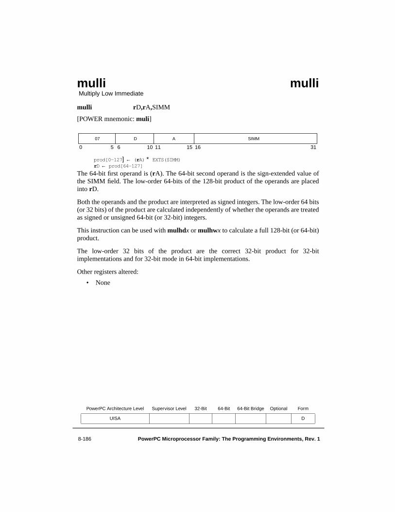
8-186 PowerPC Microprocessor Family: The Programming Environments, Rev. 1
mulli mulli Multiply Low Immediate
mulli rD,rA,SIMM
[POWER mnemonic: muli]
prod[0–127] ← (rA) ∗ EXTS(SIMM)rD ← prod[64–127]
The 64-bit first operand is (rA). The 64-bit second operand is the sign-extended value ofthe SIMM field. The low-order 64-bits of the 128-bit product of the operands are placedinto rD.
Both the operands and the product are interpreted as signed integers. The low-order 64 bits(or 32 bits) of the product are calculated independently of whether the operands are treatedas signed or unsigned 64-bit (or 32-bit) integers.
This instruction can be used with mulhdx or mulhwx to calculate a full 128-bit (or 64-bit)product.
The low-order 32 bits of the product are the correct 32-bit product for 32-bitimplementations and for 32-bit mode in 64-bit implementations.
Other registers altered:
• None
PowerPC Architecture Level Supervisor Level 32-Bit 64-Bit 64-Bit Bridge Optional Form
UISA D
0 5 6 10 11 15 16 31
SIMM07 D A

Chapter 8. Instruction Set 8-187
mullwx mullwx Multiply Low Word
mullw rD,rA,rB (OE = 0 Rc = 0)mullw. rD,rA,rB (OE = 0 Rc = 1)mullwo rD,rA,rB (OE = 1 Rc = 0) mullwo. rD,rA,rB (OE = 1 Rc = 1)
[POWER mnemonics: muls, muls., mulso, mulso.]
rD ← rA[32–63] ∗ rB[32–63]The 32-bit operands are the contents of the low-order 32 bits of rA and rB. The low-order32 bits of the 64-bit product (rA) * (rB) are placed into rD.
The low-order 32 bits of the product are the correct 32-bit product for 32-bit mode of 64-bit implementations and for 32-bit implementations. The low-order 32-bits of the productare independent of whether the operands are regarded as signed or unsigned 32-bit integers.
If OE = 1, then OV is set if the product cannot be represented in 32 bits. Both the operandsand the product are interpreted as signed integers.
This instruction can be used with mulhwx to calculate a full 64-bit product.
Note that this instruction may execute faster on some implementations if rB contains theoperand having the smaller absolute value.
Other registers altered:
• Condition Register (CR0 field):
Affected: LT, GT, EQ, SO (if Rc = 1)
Note: CR0 field may not reflect the infinitely precise result if overflow occurs (see XER below).
• XER:
Affected: SO, OV (if OE = 1)
Note: The setting of the affected bits in the XER is mode-independent, and reflects overflow of the low-order 32-bit result.
PowerPC Architecture Level Supervisor Level 32-Bit 64-Bit 64-Bit Bridge Optional Form
UISA XO
0 5 6 10 11 15 16 20 21 22 30 31
31 D A B OE 235 Rc

8-188 PowerPC Microprocessor Family: The Programming Environments, Rev. 1
nandx nandx NAND
nand rA,rS,rB (Rc = 0)nand. rA,rS,rB (Rc = 1)
rA ← ¬ ((rS) & (rB))
The contents of rS are ANDed with the contents of rB and the complemented result isplaced into rA.
nand with rS = rB can be used to obtain the one's complement.
Other registers altered:
• Condition Register (CR0 field):
Affected: LT, GT, EQ, SO (if Rc = 1)
PowerPC Architecture Level Supervisor Level 32-Bit 64-Bit 64-Bit Bridge Optional Form
UISA X
0 5 6 10 11 15 16 20 21 30 31
31 S A B 476 Rc

Chapter 8. Instruction Set 8-189
negx negx Negate
neg rD,rA (OE = 0 Rc = 0)neg. rD,rA (OE = 0 Rc = 1)nego rD,rA (OE = 1 Rc = 0)nego. rD,rA (OE = 1 Rc = 1)
rD ← ¬ (rA) + 1
The value 1 is added to the complement of the value in rA, and the resulting two’scomplement is placed into rD.
If executing in the default 64-bit mode and rA contains the most negative 64-bit number(0x8000_0000_0000_0000), the result is the most negative number and, if OE = 1, OV isset. Similarly, if executing in 32-bit mode of a 64-bit implementation (or on a 32-bitimplementation) and the low-order 32 bits of rA contains the most negative 32-bit number(0x8000_0000), the low-order 32 bits of the result contain the most negative 32-bit numberand, if OE = 1, OV is set.
Other registers altered:
• Condition Register (CR0 field):
Affected: LT, GT, EQ, SO (if Rc = 1)
• XER:
Affected: SO OV (if OE = 1)
PowerPC Architecture Level Supervisor Level 32-Bit 64-Bit 64-Bit Bridge Optional Form
UISA XO
Reserved
0 5 6 10 11 15 16 20 21 22 30 31
31 D A 0 0 0 0 0 OE 104 Rc

8-190 PowerPC Microprocessor Family: The Programming Environments, Rev. 1
norx norx NOR
nor rA,rS,rB (Rc = 0)nor. rA,rS,rB (Rc = 1)
rA ← ¬ ((rS) | (rB))
The contents of rS are ORed with the contents of rB and the complemented result is placedinto rA.
nor with rS = rB can be used to obtain the one’s complement.
Other registers altered:
• Condition Register (CR0 field):
Affected: LT, GT, EQ, SO (if Rc = 1)
Simplified mnemonics:
not rD,rS equivalent to nor rA,rS,rS
PowerPC Architecture Level Supervisor Level 32-Bit 64-Bit 64-Bit Bridge Optional Form
UISA X
0 5 6 10 11 15 16 20 21 30 31
31 S A B 124 Rc

Chapter 8. Instruction Set 8-191
orx orx OR
or rA,rS,rB (Rc = 0)or. rA,rS,rB (Rc = 1)
rA ← (rS) | (rB)
The contents of rS are ORed with the contents of rB and the result is placed into rA.
The simplified mnemonic mr (shown below) demonstrates the use of the or instruction tomove register contents.
Other registers altered:
• Condition Register (CR0 field):
Affected: LT, GT, EQ, SO (if Rc = 1)
Simplified mnemonics:
mr rA,rS equivalent to or rA,rS,rS
PowerPC Architecture Level Supervisor Level 32-Bit 64-Bit 64-Bit Bridge Optional Form
UISA X
0 5 6 10 11 15 16 20 21 30 31
31 S A B 444 Rc

8-192 PowerPC Microprocessor Family: The Programming Environments, Rev. 1
orcx orcx OR with Complement
orc rA,rS,rB (Rc = 0) orc. rA,rS,rB (Rc = 1)
rA ← (rS) | ¬ (rB)
The contents of rS are ORed with the complement of the contents of rB and the result isplaced into rA.
Other registers altered:
• Condition Register (CR0 field):
Affected: LT, GT, EQ, SO (if Rc = 1)
PowerPC Architecture Level Supervisor Level 32-Bit 64-Bit 64-Bit Bridge Optional Form
UISA X
0 5 6 10 11 15 16 20 21 30 31
31 S A B 412 Rc
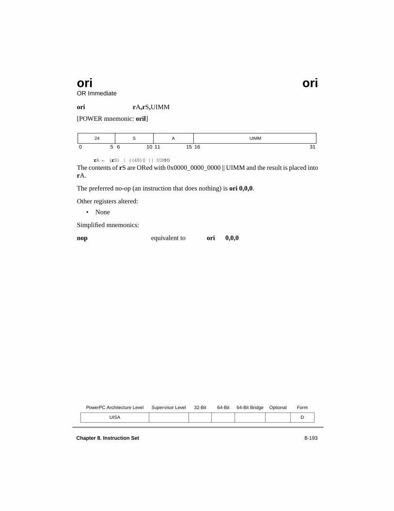
Chapter 8. Instruction Set 8-193
ori ori OR Immediate
ori rA,rS,UIMM
[POWER mnemonic: oril]
rA ← (rS) | ((48)0 || UIMM)
The contents of rS are ORed with 0x0000_0000_0000 || UIMM and the result is placed intorA.
The preferred no-op (an instruction that does nothing) is ori 0,0,0.
Other registers altered:
• None
Simplified mnemonics:
nop equivalent to ori 0,0,0
PowerPC Architecture Level Supervisor Level 32-Bit 64-Bit 64-Bit Bridge Optional Form
UISA D
0 5 6 10 11 15 16 31
24 S A UIMM
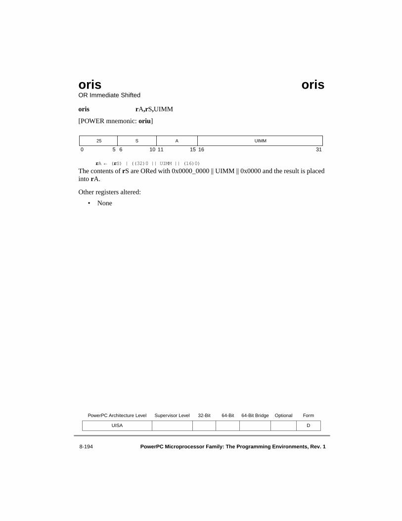
8-194 PowerPC Microprocessor Family: The Programming Environments, Rev. 1
oris orisOR Immediate Shifted
oris rA,rS,UIMM
[POWER mnemonic: oriu]
rA ← (rS) | ((32)0 || UIMM || (16)0)
The contents of rS are ORed with 0x0000_0000 || UIMM || 0x0000 and the result is placedinto rA.
Other registers altered:
• None
PowerPC Architecture Level Supervisor Level 32-Bit 64-Bit 64-Bit Bridge Optional Form
UISA D
0 5 6 10 11 15 16 31
25 S A UIMM
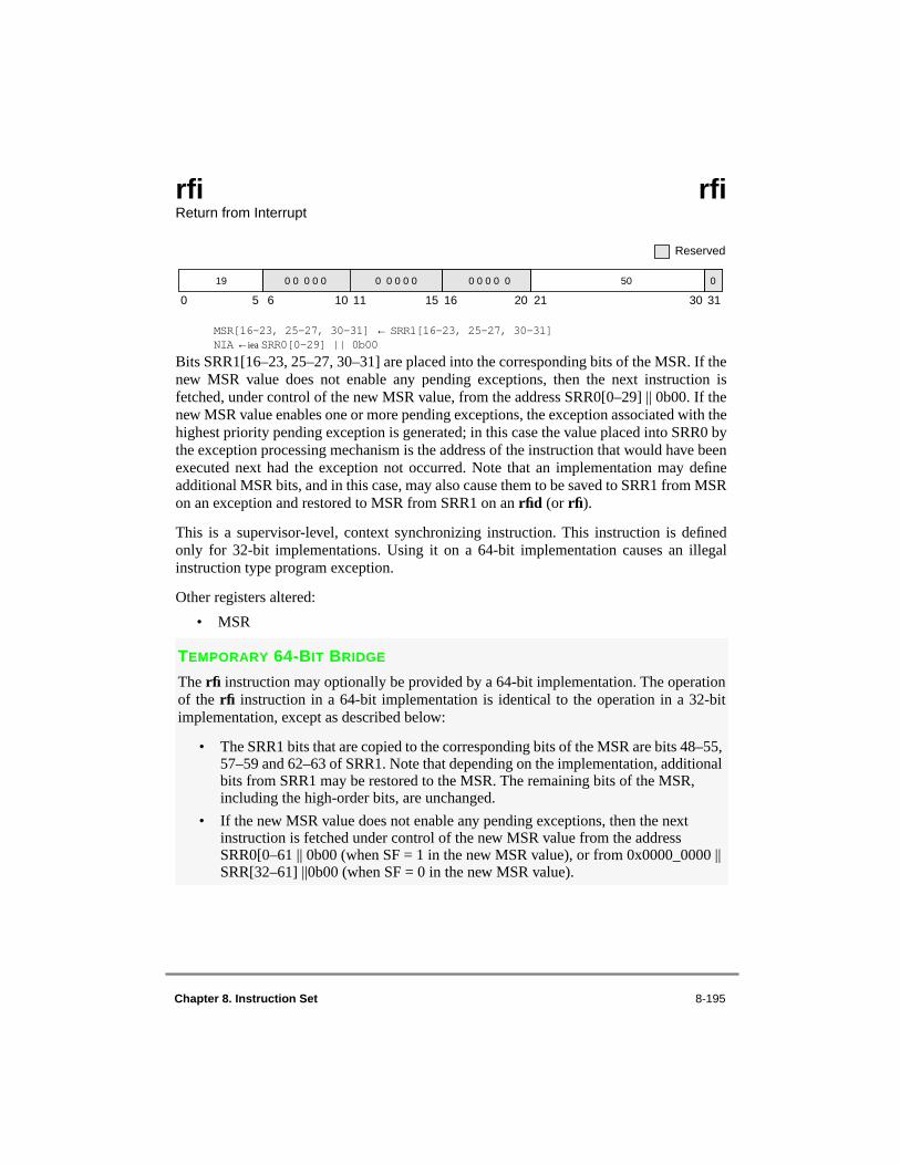
Chapter 8. Instruction Set 8-195
rfi rfiReturn from Interrupt
MSR[16–23, 25–27, 30–31] ← SRR1[16–23, 25–27, 30–31]NIA ←iea SRR0[0–29] || 0b00
Bits SRR1[16–23, 25–27, 30–31] are placed into the corresponding bits of the MSR. If thenew MSR value does not enable any pending exceptions, then the next instruction isfetched, under control of the new MSR value, from the address SRR0[0–29] || 0b00. If thenew MSR value enables one or more pending exceptions, the exception associated with thehighest priority pending exception is generated; in this case the value placed into SRR0 bythe exception processing mechanism is the address of the instruction that would have beenexecuted next had the exception not occurred. Note that an implementation may defineadditional MSR bits, and in this case, may also cause them to be saved to SRR1 from MSRon an exception and restored to MSR from SRR1 on an rfid (or rfi).
This is a supervisor-level, context synchronizing instruction. This instruction is definedonly for 32-bit implementations. Using it on a 64-bit implementation causes an illegalinstruction type program exception.
Other registers altered:
• MSR
TEMPORARY 64-BIT BRIDGE
The rfi instruction may optionally be provided by a 64-bit implementation. The operationof the rfi instruction in a 64-bit implementation is identical to the operation in a 32-bitimplementation, except as described below:
• The SRR1 bits that are copied to the corresponding bits of the MSR are bits 48–55, 57–59 and 62–63 of SRR1. Note that depending on the implementation, additional bits from SRR1 may be restored to the MSR. The remaining bits of the MSR, including the high-order bits, are unchanged.
• If the new MSR value does not enable any pending exceptions, then the next instruction is fetched under control of the new MSR value from the address SRR0[0–61 || 0b00 (when SF = 1 in the new MSR value), or from 0x0000_0000 || SRR[32–61] ||0b00 (when SF = 0 in the new MSR value).
0 0 0 0 0 50 0
Reserved
0 5 6 10 11 15 16 20 21 30 31
19 0 0 0 0 0 0 0 0 0 0

8-196 PowerPC Microprocessor Family: The Programming Environments, Rev. 1
When the optional rfi instruction is provided in a 64-bit implementation, the optionalmtmsr instruction is also provided. Refer to the mtmsr instruction description foradditional detail about the operation of the mtmsr instruction in 64-bit implementations.
PowerPC Architecture Level Supervisor Level 32-Bit 64-Bit 64-Bit Bridge Optional Form
OEA √ √ √ XL

Chapter 8. Instruction Set 8-197
rfid 64-Bit Implementations Only rfidReturn from Interrupt Double Word
MSR[0, 48–55, 57–59, 62–63] ← SRR1[0, 48–55, 57–59, 62–63]NIA ←iea SRR0[0–61] || 0b00
Bits SRR1[0, 48–55, 57–59, 62–63] are placed into the corresponding bits of the MSR. Ifthe new MSR value does not enable any pending exceptions, then the next instruction isfetched, under control of the new MSR value, from the address SRR0[0–61] || 0b00 (when MSR[SF] = 1) or 0x0000_0000 || SRR0[32–61] || 0b00 (when MSR[SF] = 0). If the newMSR value enables one or more pending exceptions, the exception associated with thehighest priority pending exception is generated; in this case the value placed into SRR0 bythe exception processing mechanism is the address of the instruction that would have beenexecuted next had the exception not occurred. Note that an implementation may defineadditional MSR bits, and in this case, may also cause them to be saved to SRR1 from MSRon an exception and restored to MSR from SRR1 on an rfid.
This is a supervisor-level, context synchronizing instruction.
This instruction is defined only for 64-bit implementations. Using it on a 32-bitimplementation causes an illegal instruction type program exception.
Other registers altered:
• MSR
PowerPC Architecture Level Supervisor Level 32-Bit 64-Bit 64-Bit Bridge Optional Form
OEA √ √ XL
Reserved
0 5 6 10 11 15 16 20 21 30 31
19 0 0 0 0 0 0 0 0 0 0 0 0 0 0 0 18 0

8-198 PowerPC Microprocessor Family: The Programming Environments, Rev. 1
rldclx 64-Bit Implementations Only rldclxRotate Left Double Word then Clear Left
rldcl rA,rS,rB,MB (Rc = 0)rldcl. rA,rS,rB,MB (Rc = 1)
n ← rB[58–63]r ← ROTL[64](rS, n)b ← mb[5] || mb[0–4]m ← MASK(b, 63)rA ← r & m
The contents of rS are rotated left the number of bits specified by operand in the low-ordersix bits of rB. A mask is generated having 1 bits from bit MB through bit 63 and 0 bitselsewhere. The rotated data is ANDed with the generated mask and the result is placed intorA.
This instruction is defined only for 64-bit implementations. Using it on a 32-bitimplementation will cause the system illegal instruction error handler to be invoked.
Note that the rldcl instruction can be used to extract and rotate bit fields using the methodsshown below:
• To extract an n-bit field, that starts at variable bit position b in register rS, right-justified into rA (clearing the remaining 64 – n bits of rA), set the low-order six bits of rB to b + n and MB = 64 – n.
• To rotate the contents of a register left by variable n bits, set the low-order six bits of rB to n and MB = 0, and to shift the contents of a register right, set the low-order six bits of rB to(64 – n), and MB = 0.
Other registers altered:
• Condition Register (CR0 field):
Affected: LT, GT, EQ, SO (if Rc = 1)
Simplified mnemonics:
rotld rA,rS,rB equivalent to rldcl rA,rS,rB,0
PowerPC Architecture Level Supervisor Level 32-Bit 64-Bit 64-Bit Bridge Optional Form
UISA √ MDS
0 5 6 10 11 15 16 20 21 26 27 30 31
30 S A B mb* 8 Rc
*Note: This is a split field.
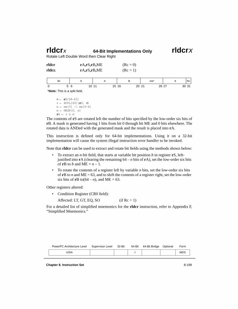
Chapter 8. Instruction Set 8-199
rldcrx 64-Bit Implementations Only rldcrxRotate Left Double Word then Clear Right
rldcr rA,rS,rB,ME (Rc = 0)rldcr. rA,rS,rB,ME (Rc = 1)
n ← rB[58–63]r ← ROTL[64](rS, n)e ← me[5] || me[0–4]m ← MASK(0, e)rA ← r & m
The contents of rS are rotated left the number of bits specified by the low-order six bits ofrB. A mask is generated having 1 bits from bit 0 through bit ME and 0 bits elsewhere. Therotated data is ANDed with the generated mask and the result is placed into rA.
This instruction is defined only for 64-bit implementations. Using it on a 32-bitimplementation will cause the system illegal instruction error handler to be invoked.
Note that rldcr can be used to extract and rotate bit fields using the methods shown below:
• To extract an n-bit field, that starts at variable bit position b in register rS, left-justified into rA (clearing the remaining 64 – n bits of rA), set the low-order six bits of rB to b and ME = n – 1.
• To rotate the contents of a register left by variable n bits, set the low-order six bits of rB to n and ME = 63, and to shift the contents of a register right, set the low-order six bits of rB to(64 – n), and ME = 63.
Other registers altered:
• Condition Register (CR0 field):
Affected: LT, GT, EQ, SO (if Rc = 1)
For a detailed list of simplified mnemonics for the rldcr instruction, refer to Appendix F,“Simplified Mnemonics.”
PowerPC Architecture Level Supervisor Level 32-Bit 64-Bit 64-Bit Bridge Optional Form
UISA √ MDS
0 5 6 10 11 15 16 20 21 26 27 30 31
30 S A B me* 9 Rc
*Note: This is a split field.

8-200 PowerPC Microprocessor Family: The Programming Environments, Rev. 1
rldicx 64-Bit Implementations Only rldicxRotate Left Double Word Immediate then Clear
rldic rA,rS,SH,MB (Rc = 0)rldic. rA,rS,SH,MB (Rc = 1)
n ← sh[5] || sh[0–4]r ← ROTL[64](rS, n)b ← mb[5] || mb[0–4]m ← MASK(b, ¬ n)rA ← r & m
The contents of rS are rotated left the number of bits specified by operand SH. A mask isgenerated having 1 bits from bit MB through bit 63 – SH and 0 bits elsewhere. The rotateddata is ANDed with the generated mask and the result is placed into rA.
This instruction is defined only for 64-bit implementations. Using it on a 32-bitimplementation will cause the system illegal instruction error handler to be invoked.
Note that rldic can be used to clear and shift bit fields using the methods shown below:
• To clear the high-order b bits of the contents of a register and then shift the result left by n bits, set SH = n and MB = b – n.
• To clear the high-order n bits of a register, set SH = 0 and MB = n.
Other registers altered:
• Condition Register (CR0 field):
Affected: LT, GT, EQ, SO (if Rc = 1)
Simplified mnemonics:
clrlsldi rA,rS,b,n equivalent to rldic rA,rS,n,b – n
For a more detailed list of simplified mnemonics for the rldic instruction, refer toAppendix F, “Simplified Mnemonics.”
PowerPC Architecture Level Supervisor Level 32-Bit 64-Bit 64-Bit Bridge Optional Form
UISA √ MD
0 5 6 10 11 15 16 20 21 26 27 29 30 31
30 S A sh* mb* 2 sh* Rc
*Note: This is a split field.
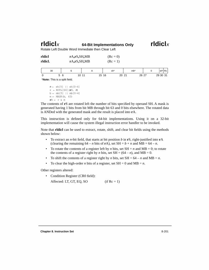
Chapter 8. Instruction Set 8-201
rldiclx 64-Bit Implementations Only rldiclxRotate Left Double Word Immediate then Clear Left
rldicl rA,rS,SH,MB (Rc = 0)rldicl. rA,rS,SH,MB (Rc = 1)
n ← sh[5] || sh[0–4]r ← ROTL[64](rS, n)b ← mb[5] || mb[0–4]m ← MASK(b, 63)rA ← r & m
The contents of rS are rotated left the number of bits specified by operand SH. A mask isgenerated having 1 bits from bit MB through bit 63 and 0 bits elsewhere. The rotated datais ANDed with the generated mask and the result is placed into rA.
This instruction is defined only for 64-bit implementations. Using it on a 32-bitimplementation will cause the system illegal instruction error handler to be invoked.
Note that rldicl can be used to extract, rotate, shift, and clear bit fields using the methodsshown below:
• To extract an n-bit field, that starts at bit position b in rS, right-justified into rA (clearing the remaining 64 – n bits of rA), set SH = b + n and MB = 64 – n.
• To rotate the contents of a register left by n bits, set SH = n and MB = 0; to rotate the contents of a register right by n bits, set SH = (64 – n), and MB = 0.
• To shift the contents of a register right by n bits, set SH = 64 – n and MB = n.
• To clear the high-order n bits of a register, set SH = 0 and MB = n.
Other registers altered:
• Condition Register (CR0 field):
Affected: LT, GT, EQ, SO (if Rc = 1)
0 5 6 10 11 15 16 20 21 26 27 29 30 31
30 S A sh* mb* 0 sh* Rc
*Note: This is a split field.

8-202 PowerPC Microprocessor Family: The Programming Environments, Rev. 1
Simplified mnemonics:
extrdi rA,rS,n,b (n > 0) equivalent to rldicl rA,rS,b + n,64 – nrotldi rA,rS,n equivalent to rldicl rA,rS,n,0rotrdi rA,rS,n equivalent to rldicl rA,rS,64 – n,0srdi rA,rS,n (n < 64) equivalent to rldicl rA,rS,64 – n,n clrldi rA,rS,n (n < 64) equivalent to rldicl rA,rS,0,n
PowerPC Architecture Level Supervisor Level 32-Bit 64-Bit 64-Bit Bridge Optional Form
UISA
√
MD
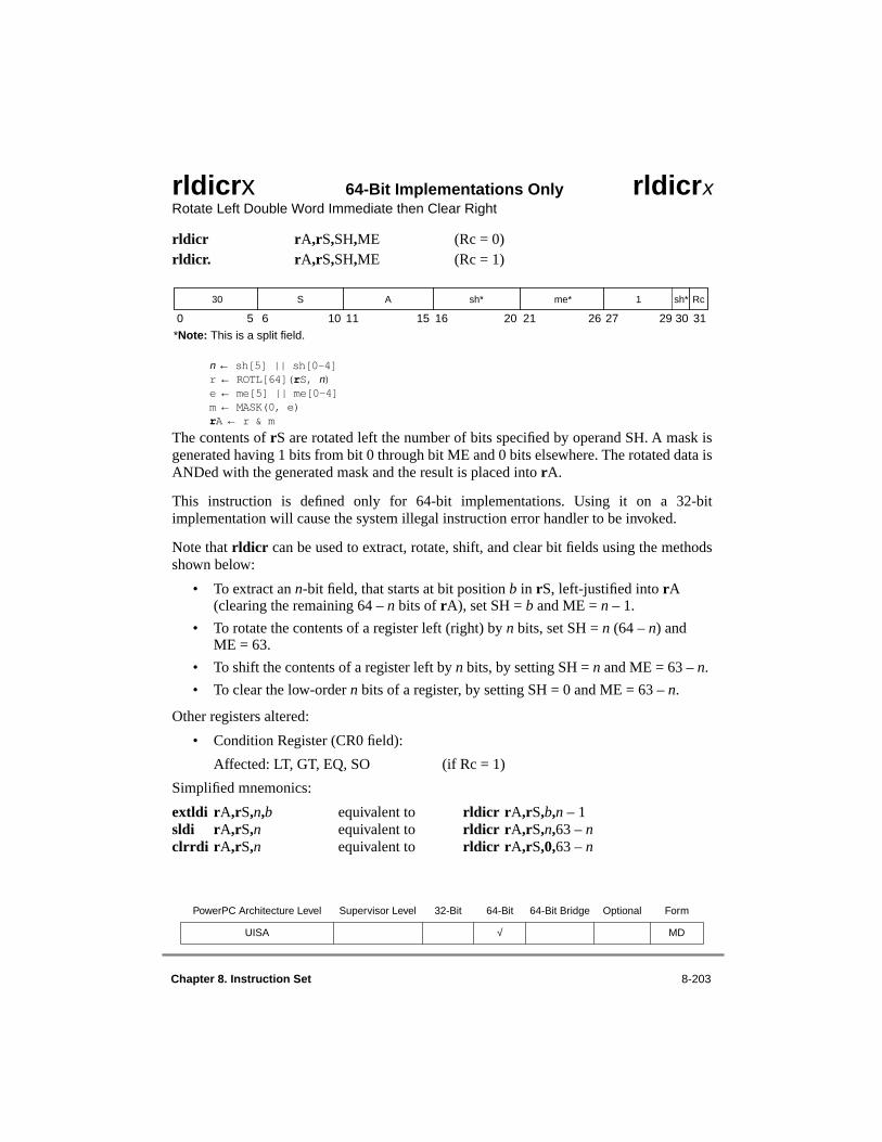
Chapter 8. Instruction Set
8-203
rldicr
x
64-Bit Implementations Only
rldicr
x
Rotate Left Double Word Immediate then Clear Right
rldicr r
A
,r
S
,
SH
,
ME (Rc = 0)
rldicr. r
A
,r
S
,
SH
,
ME (Rc = 1)
n
←
sh[5] || sh[0–4]r
←
ROTL[64](
r
S,
n
)e
←
me[5] || me[0–4]m
←
MASK(0, e)
r
A
←
r & m
The contents of
r
S are rotated left the number of bits specified by operand SH. A mask isgenerated having 1 bits from bit 0 through bit ME and 0 bits elsewhere. The rotated data isANDed with the generated mask and the result is placed into
r
A.
This instruction is defined only for 64-bit implementations. Using it on a 32-bitimplementation will cause the system illegal instruction error handler to be invoked.
Note that
rldicr
can be used to extract, rotate, shift, and clear bit fields using the methodsshown below:
• To extract an
n
-bit field, that starts at bit position
b
in
r
S, left-justified into
r
A (clearing the remaining 64 –
n
bits of
r
A), set SH =
b
and ME =
n
– 1.
• To rotate the contents of a register left (right) by
n
bits, set SH =
n
(64
– n
) and ME = 63.
• To shift the contents of a register left by
n
bits, by setting SH =
n
and ME = 63 –
n
.
• To clear the low-order
n
bits of a register, by setting SH = 0 and ME = 63 –
n
.
Other registers altered:
• Condition Register (CR0 field):
Affected: LT, GT, EQ, SO (if Rc = 1)
Simplified mnemonics:
extldi r
A
,r
S
,
n
,
b
equivalent to
rldicr r
A
,r
S
,
b
,
n
– 1
sldi r
A
,r
S
,
n
equivalent to
rldicr r
A
,r
S
,
n
,
63
–
n
clrrdi r
A
,r
S
,
n
equivalent to
rldicr r
A
,r
S
,0,
63 –
n
PowerPC Architecture Level Supervisor Level 32-Bit 64-Bit 64-Bit Bridge Optional Form
UISA
√
MD
0 5 6 10 11 15 16 20 21 26 27 29 30 31
30 S A sh* me* 1 sh* Rc
*Note: This is a split field.

8-204
PowerPC Microprocessor Family: The Programming Environments, Rev. 1
rldimi
x
64-Bit Implementations Only
rldimi
x
Rotate Left Double Word Immediate then Mask Insert
rldimi r
A
,r
S
,
SH
,
MB (Rc = 0)
rldimi. r
A
,r
S
,
SH
,
MB (Rc = 1)
n
←
sh[5] || sh[0–4]r
←
ROTL[64](
r
S,
n
)b
←
mb[5] || mb[0–4]m
←
MASK(b, ¬
n
)
r
A
←
(r & m) | (
r
A & ¬ m)
The contents of
r
S are rotated left the number of bits specified by operand SH. A mask isgenerated having 1 bits from bit MB through bit 63 – SH and 0 bits elsewhere. The rotateddata is inserted into
r
A under control of the generated mask.
This instruction is defined only for 64-bit implementations. Using it on a 32-bitimplementation will cause the system illegal instruction error handler to be invoked.
Note that
rldimi can be used to insert an n-bit field, that is right-justified in rS, into rAstarting at bit position b, by setting SH = 64 – (b + n) and MB = b.
Other registers altered:
• Condition Register (CR0 field):
Affected: LT, GT, EQ, SO (if Rc = 1)
Simplified mnemonics:
insrdi rA,rS,n,b equivalent to rldimirA,rS,64 – (b + n),b
For a more detailed list of simplified mnemonics for the rldimi instruction, refer toAppendix F, “Simplified Mnemonics.”
PowerPC Architecture Level Supervisor Level 32-Bit 64-Bit 64-Bit Bridge Optional Form
UISA √ MD
0 5 6 10 11 15 16 20 21 26 27 29 30 31
30 S A sh* mb* 3 sh* Rc
*Note: This is a split field.
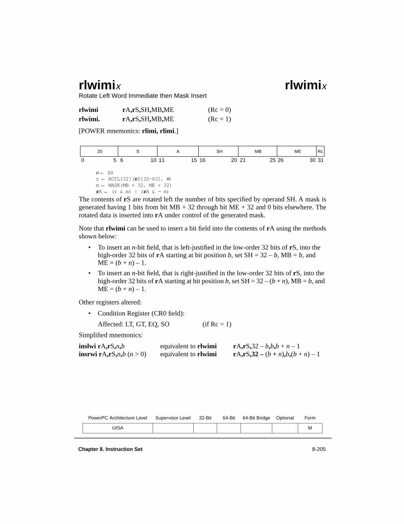
Chapter 8. Instruction Set 8-205
rlwimix rlwimix Rotate Left Word Immediate then Mask Insert
rlwimi rA,rS,SH,MB,ME (Rc = 0)rlwimi. rA,rS,SH,MB,ME (Rc = 1)
[POWER mnemonics: rlimi, rlimi.]
n ← SHr ← ROTL[32](rS[32–63], n)m ← MASK(MB + 32, ME + 32)rA ← (r & m) | (rA & ¬ m)
The contents of rS are rotated left the number of bits specified by operand SH. A mask isgenerated having 1 bits from bit MB + 32 through bit ME + 32 and 0 bits elsewhere. Therotated data is inserted into rA under control of the generated mask.
Note that rlwimi can be used to insert a bit field into the contents of rA using the methodsshown below:
• To insert an n-bit field, that is left-justified in the low-order 32 bits of rS, into the high-order 32 bits of rA starting at bit position b, set SH = 32 – b, MB = b, and ME = (b + n) – 1.
• To insert an n-bit field, that is right-justified in the low-order 32 bits of rS, into the high-order 32 bits of rA starting at bit position b, set SH = 32 – (b + n), MB = b, and ME = (b + n) – 1.
Other registers altered:
• Condition Register (CR0 field):
Affected: LT, GT, EQ, SO (if Rc = 1)
Simplified mnemonics:
inslwi rA,rS,n,b equivalent to rlwimi rA,rS,32 – b,b,b + n – 1insrwi rA,rS,n,b (n > 0) equivalent to rlwimi rA,rS,32 – (b + n),b,(b + n) – 1
PowerPC Architecture Level Supervisor Level 32-Bit 64-Bit 64-Bit Bridge Optional Form
UISA M
0 5 6 10 11 15 16 20 21 25 26 30 31
20 S A SH MB ME Rc
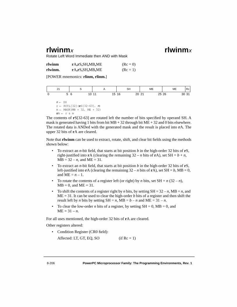
8-206 PowerPC Microprocessor Family: The Programming Environments, Rev. 1
rlwinmx rlwinmx Rotate Left Word Immediate then AND with Mask
rlwinm rA,rS,SH,MB,ME (Rc = 0)rlwinm. rA,rS,SH,MB,ME (Rc = 1)
[POWER mnemonics: rlinm, rlinm.]
n ← SHr ← ROTL[32](rS[32–63], n)m ← MASK(MB + 32, ME + 32)rA ← r & m
The contents of rS[32-63] are rotated left the number of bits specified by operand SH. Amask is generated having 1 bits from bit MB + 32 through bit ME + 32 and 0 bits elsewhere.The rotated data is ANDed with the generated mask and the result is placed into rA. Theupper 32 bits of rA are cleared.
Note that rlwinm can be used to extract, rotate, shift, and clear bit fields using the methodsshown below:
• To extract an n-bit field, that starts at bit position b in the high-order 32 bits of rS, right-justified into rA (clearing the remaining 32 – n bits of rA), set SH = b + n, MB = 32 – n, and ME = 31.
• To extract an n-bit field, that starts at bit position b in the high-order 32 bits of rS, left-justified into rA (clearing the remaining 32 – n bits of rA), set SH = b, MB = 0, and ME = n – 1.
• To rotate the contents of a register left (or right) by n bits, set SH = n (32 – n), MB = 0, and ME = 31.
• To shift the contents of a register right by n bits, by setting SH = 32 – n, MB = n, and ME = 31. It can be used to clear the high-order b bits of a register and then shift the result left by n bits by setting SH = n, MB = b – n and ME = 31 – n.
• To clear the low-order n bits of a register, by setting SH = 0, MB = 0, and ME = 31 – n.
For all uses mentioned, the high-order 32 bits of rA are cleared.
Other registers altered:
• Condition Register (CR0 field):
Affected: LT, GT, EQ, SO (if Rc = 1)
0 5 6 10 11 15 16 20 21 25 26 30 31
21 S A SH MB ME Rc

Chapter 8. Instruction Set 8-207
Simplified mnemonics:
extlwi rA,rS,n,b (n > 0) equivalent to rlwinm rA,rS,b,0,n – 1extrwi rA,rS,n,b (n > 0) equivalent to rlwinm rA,rS,b + n,32 – n,31rotlwi rA,rS,n equivalent to rlwinm rA,rS,n,0,31rotrwi rA,rS,n equivalent to rlwinm rA,rS,32 – n,0,31slwi rA,rS,n (n < 32) equivalent to rlwinm rA,rS,n,0,31–nsrwi rA,rS,n (n < 32) equivalent to rlwinm rA,rS,32 – n,n,31 clrlwi rA,rS,n (n < 32) equivalent to rlwinm rA,rS,0,n,31clrrwi rA,rS,n (n < 32) equivalent to rlwinm rA,rS,0,0,31 – nclrlslwi rA,rS,b,n (n ≤ b < 32) equivalent to rlwinm rA,rS,n,b – n,31 – n
PowerPC Architecture Level Supervisor Level 32-Bit 64-Bit 64-Bit Bridge Optional Form
UISA M

8-208 PowerPC Microprocessor Family: The Programming Environments, Rev. 1
rlwnmx rlwnmx Rotate Left Word then AND with Mask
rlwnm rA,rS,rB,MB,ME (Rc = 0)rlwnm. rA,rS,rB,MB,ME (Rc = 1)
[POWER mnemonics: rlnm, rlnm.]
n ← rB[59–63]r ← ROTL[32](rS[32–63], n)m ← MASK(MB + 32, ME + 32)rA ← r & m
The contents of rS are rotated left the number of bits specified by the low-order five bits ofrB. A mask is generated having 1 bits from bit MB + 32 through bit ME + 32 and 0 bitselsewhere. The rotated data is ANDed with the generated mask and the result is placed intorA.
Note that rlwnm can be used to extract and rotate bit fields using the methods shown asfollows:
• To extract an n-bit field, that starts at variable bit position b in the high-order 32 bits of rS, right-justified into rA (clearing the remaining 32 – n bits of rA), by setting the low-order five bits of rB to b + n, MB = 32 – n, and ME = 31.
• To extract an n-bit field, that starts at variable bit position b in the high-order 32 bits of rS, left-justified into rA (clearing the remaining 32 – n bits of rA), by setting the low-order five bits of rB to b, MB = 0, and ME = n – 1.
• To rotate the contents of a register left (or right) by n bits, by setting the low-order five bits of rB to n (32 – n), MB = 0, and ME = 31.
For all uses mentioned, the high-order 32 bits of rA are cleared.
Other registers altered:
• Condition Register (CR0 field):
Affected: LT, GT, EQ, SO (if Rc = 1)
Simplified mnemonics:
rotlw rA,rS,rB equivalent to rlwnmrA,rS,rB,0,31
PowerPC Architecture Level Supervisor Level 32-Bit 64-Bit 64-Bit Bridge Optional Form
UISA M
0 5 6 10 11 15 16 20 21 25 26 30 31
23 S A B MB ME Rc

Chapter 8. Instruction Set 8-209
sc scSystem Call
[POWER mnemonic: svca]
In the PowerPC UISA, the sc instruction calls the operating system to perform a service.When control is returned to the program that executed the system call, the content of theregisters depends on the register conventions used by the program providing the systemservice.
This instruction is context synchronizing, as described in Section 4.1.5.1, “ContextSynchronizing Instructions.”
Other registers altered:
• Dependent on the system service
In PowerPC OEA, the sc instruction does the following:
SRR0 ←iea CIA + 4SRR1[33–36, 42–47] ← 0SRR1[0, 48–55, 57–59, 62–63] ← MSR[0, 48–55, 57–59, 62–63]MSR ← new_value (see below)NIA ←iea base_ea + 0xC00 (see below)
The EA of the instruction following the sc instruction is placed into SRR0. Bits 0, 48–55,57–59, and 62–63 of the MSR are placed into the corresponding bits of SRR1, and bits33–36 and 42–47 of SRR1 are set to undefined values. Note that an implementation maydefine additional MSR bits, and in this case, may also cause them to be saved to SRR1 fromMSR on an exception and restored to MSR from SRR1 on an rfid (or rfi).
Then a system call exception is generated. The exception causes the MSR to be altered asdescribed in Section 6.4, “Exception Definitions.”
The exception causes the next instruction to be fetched from offset 0xC00 from the physicalbase address determined by the new setting of MSR[IP].
Other registers altered:
• SRR0• SRR1• MSR
PowerPC Architecture Level Supervisor Level 32-Bit 64-Bit 64-Bit Bridge Optional Form
UISA/OEA SC
0 0 0 0 0 0 0 0 0 0 0 0 0 0 1 0
Reserved
0 5 6 10 11 15 16 29 30 31
17 0 0 0 0 0 0 0 0 0 0
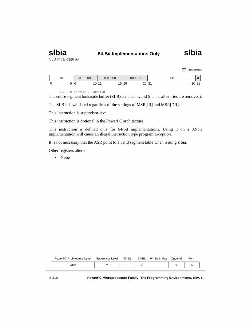
8-210 PowerPC Microprocessor Family: The Programming Environments, Rev. 1
slbia 64-Bit Implementations Only slbiaSLB Invalidate All
All SLB entries ← invalid
The entire segment lookaside buffer (SLB) is made invalid (that is, all entries are removed).
The SLB is invalidated regardless of the settings of MSR[IR] and MSR[DR].
This instruction is supervisor-level.
This instruction is optional in the PowerPC architecture.
This instruction is defined only for 64-bit implementations. Using it on a 32-bitimplementation will cause an illegal instruction type program exception.
It is not necessary that the ASR point to a valid segment table when issuing slbia.
Other registers altered:
• None
PowerPC Architecture Level Supervisor Level 32-Bit 64-Bit 64-Bit Bridge Optional Form
OEA √ √ √ X
0 5 6 10 11 15 16 20 21 30 31
Reserved
31 0 0 0 0 0 0 0 0 0 0 0 0 0 0 0 498 0

Chapter 8. Instruction Set 8-211
slbie 64-Bit Implementations Only slbieSLB Invalidate Entry
slbie rB
EA ← (rB)if SLB entry exists for EA, thenSLB entry ← invalid
EA is the contents of rB. If the segment lookaside buffer (SLB) contains an entrycorresponding to EA, that entry is made invalid (that is, removed from the SLB).
The SLB search is done regardless of the settings of MSR[IR] and MSR[DR].
Block address translation for EA, if any, is ignored.
This instruction is supervisor-level and optional in the PowerPC architecture.
This instruction is defined only for 64-bit implementations. Using it on a 32-bitimplementation will cause an illegal instruction type program exception.
It is not necessary that the ASR point to a valid segment table when issuing slbie.
Note that bits 11–15 of this instruction (ordinarily the position of an rA field) must be zero.This provides implementations the option of using (rA|0) + rB address arithmetic for thisinstruction.
Other registers altered:
• None
PowerPC Architecture Level Supervisor Level 32-Bit 64-Bit 64-Bit Bridge Optional Form
OEA √ √ √ X
0 5 6 10 11 15 16 20 21 30 31
Reserved
31 0 0 0 0 0 0 0 0 0 0 B 434 0
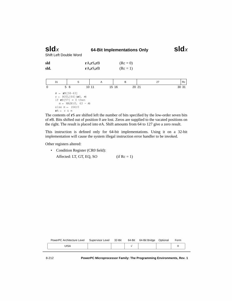
8-212 PowerPC Microprocessor Family: The Programming Environments, Rev. 1
sldx 64-Bit Implementations Only sldxShift Left Double Word
sld rA,rS,rB (Rc = 0)sld. rA,rS,rB (Rc = 1)
n ← rB[58–63]r ← ROTL[64](rS, n)if rB[57] = 0 then
m ← MASK(0, 63 – n)else m ← (64)0rA ← r & m
The contents of rS are shifted left the number of bits specified by the low-order seven bitsof rB. Bits shifted out of position 0 are lost. Zeros are supplied to the vacated positions onthe right. The result is placed into rA. Shift amounts from 64 to 127 give a zero result.
This instruction is defined only for 64-bit implementations. Using it on a 32-bitimplementation will cause the system illegal instruction error handler to be invoked.
Other registers altered:
• Condition Register (CR0 field):
Affected: LT, GT, EQ, SO (if Rc = 1)
PowerPC Architecture Level Supervisor Level 32-Bit 64-Bit 64-Bit Bridge Optional Form
UISA √ X
0 5 6 10 11 15 16 20 21 30 31
31 S A B 27 Rc

Chapter 8. Instruction Set 8-213
slwx slwx Shift Left Word
slw rA,rS,rB (Rc = 0)slw. rA,rS,rB (Rc = 1)
[POWER mnemonics: sl, sl.]
n ← rB[59–63]r ← ROTL[32](rS[32–63], n)if rB[58] = 0 thenm ← MASK(32, 63 – n)else m ← (64)0rA ← r & m
The contents of the low-order 32 bits of rS are shifted left the number of bits specified bythe low-order six bits of rB. Bits shifted out of position 32 are lost. Zeros are supplied tothe vacated positions on the right. The 32-bit result is placed into the low-order 32 bits ofrA. The high-order 32 bits of rA are cleared. Shift amounts from 32 to 63 give a zero result.
Other registers altered:
• Condition Register (CR0 field):
Affected: LT, GT, EQ, SO (if Rc = 1)
PowerPC Architecture Level Supervisor Level 32-Bit 64-Bit 64-Bit Bridge Optional Form
UISA X
0 5 6 10 11 15 16 20 21 30 31
31 S A B 24 Rc
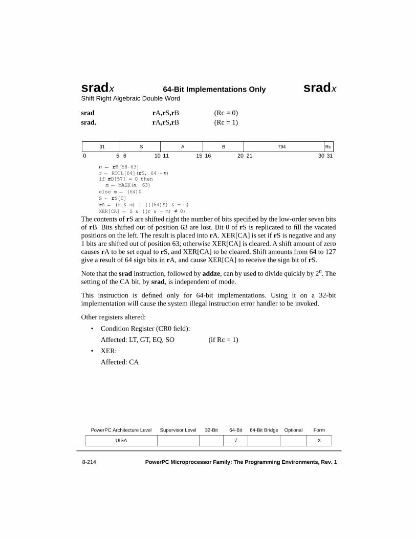
8-214 PowerPC Microprocessor Family: The Programming Environments, Rev. 1
sradx 64-Bit Implementations Only sradxShift Right Algebraic Double Word
srad rA,rS,rB (Rc = 0)srad. rA,rS,rB (Rc = 1)
n ← rB[58–63]r ← ROTL[64](rS, 64 – n)if rB[57] = 0 then
m ← MASK(n, 63)else m ← (64)0S ← rS[0]rA ← (r & m) | (((64)S) & ¬ m)XER[CA] ← S & ((r & ¬ m) ≠ 0)
The contents of rS are shifted right the number of bits specified by the low-order seven bitsof rB. Bits shifted out of position 63 are lost. Bit 0 of rS is replicated to fill the vacatedpositions on the left. The result is placed into rA. XER[CA] is set if rS is negative and any1 bits are shifted out of position 63; otherwise XER[CA] is cleared. A shift amount of zerocauses rA to be set equal to rS, and XER[CA] to be cleared. Shift amounts from 64 to 127give a result of 64 sign bits in rA, and cause XER[CA] to receive the sign bit of rS.
Note that the srad instruction, followed by addze, can by used to divide quickly by 2n. Thesetting of the CA bit, by srad, is independent of mode.
This instruction is defined only for 64-bit implementations. Using it on a 32-bitimplementation will cause the system illegal instruction error handler to be invoked.
Other registers altered:
• Condition Register (CR0 field):
Affected: LT, GT, EQ, SO (if Rc = 1)
• XER:
Affected: CA
PowerPC Architecture Level Supervisor Level 32-Bit 64-Bit 64-Bit Bridge Optional Form
UISA √ X
0 5 6 10 11 15 16 20 21 30 31
31 S A B 794 Rc
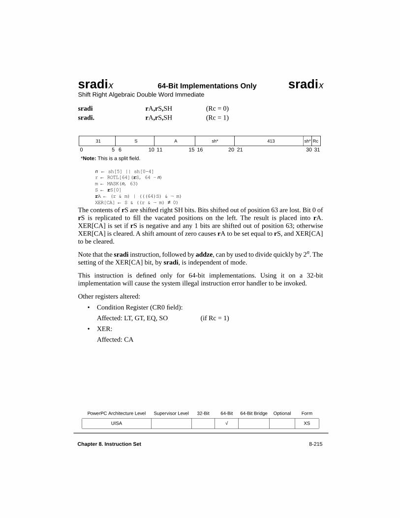
Chapter 8. Instruction Set 8-215
sradix 64-Bit Implementations Only sradixShift Right Algebraic Double Word Immediate
sradi rA,rS,SH (Rc = 0)sradi. rA,rS,SH (Rc = 1)
n ← sh[5] || sh[0–4]r ← ROTL[64](rS, 64 – n)m ← MASK(n, 63)S ← rS[0]rA ← (r & m) | (((64)S) & ¬ m)XER[CA] ← S & ((r & ¬ m) ≠ 0)
The contents of rS are shifted right SH bits. Bits shifted out of position 63 are lost. Bit 0 ofrS is replicated to fill the vacated positions on the left. The result is placed into rA.XER[CA] is set if rS is negative and any 1 bits are shifted out of position 63; otherwiseXER[CA] is cleared. A shift amount of zero causes rA to be set equal to rS, and XER[CA]to be cleared.
Note that the sradi instruction, followed by addze, can by used to divide quickly by 2n. Thesetting of the XER[CA] bit, by sradi, is independent of mode.
This instruction is defined only for 64-bit implementations. Using it on a 32-bitimplementation will cause the system illegal instruction error handler to be invoked.
Other registers altered:
• Condition Register (CR0 field):
Affected: LT, GT, EQ, SO (if Rc = 1)
• XER:
Affected: CA
PowerPC Architecture Level Supervisor Level 32-Bit 64-Bit 64-Bit Bridge Optional Form
UISA √ XS
0 5 6 10 11 15 16 20 21 30 31
31 S A sh* 413 sh* Rc
*Note: This is a split field.
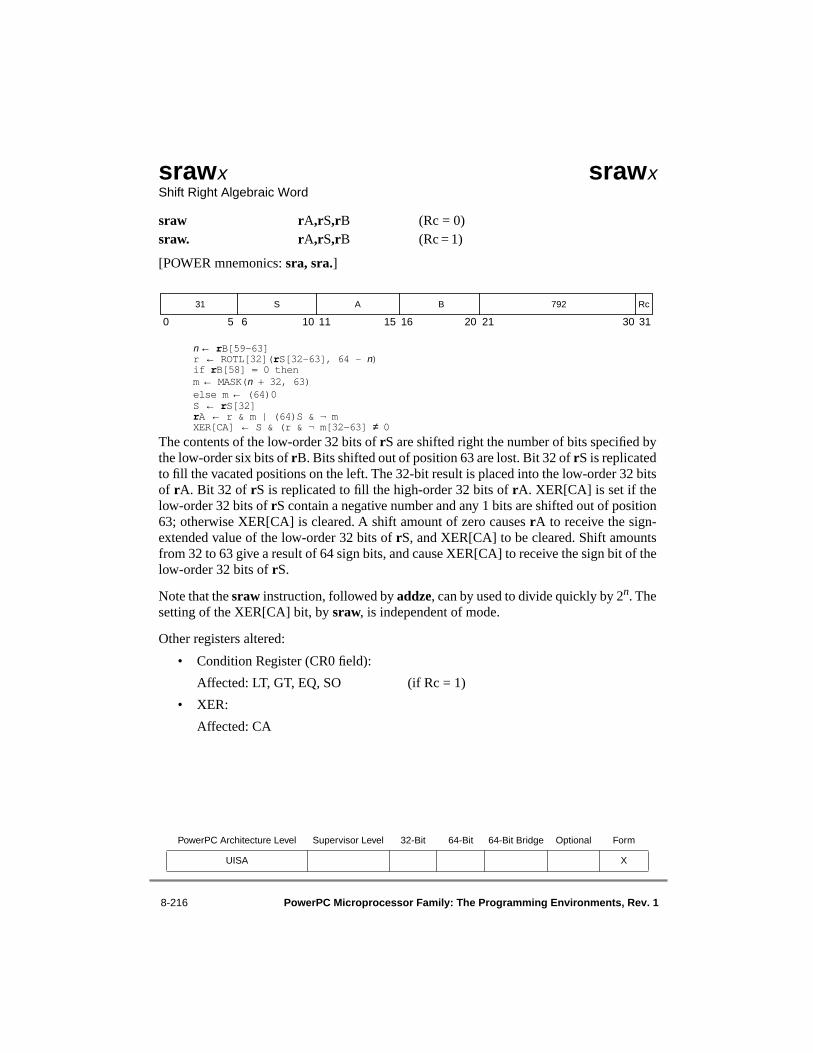
8-216 PowerPC Microprocessor Family: The Programming Environments, Rev. 1
srawx srawx Shift Right Algebraic Word
sraw rA,rS,rB (Rc = 0)sraw. rA,rS,rB (Rc = 1)
[POWER mnemonics: sra, sra.]
n ← rB[59–63]r ← ROTL[32](rS[32–63], 64 – n)if rB[58] = 0 thenm ← MASK(n + 32, 63)else m ← (64)0S ← rS[32]rA ← r & m | (64)S & ¬ mXER[CA] ← S & (r & ¬ m[32–63] ≠ 0
The contents of the low-order 32 bits of rS are shifted right the number of bits specified bythe low-order six bits of rB. Bits shifted out of position 63 are lost. Bit 32 of rS is replicatedto fill the vacated positions on the left. The 32-bit result is placed into the low-order 32 bitsof rA. Bit 32 of rS is replicated to fill the high-order 32 bits of rA. XER[CA] is set if thelow-order 32 bits of rS contain a negative number and any 1 bits are shifted out of position63; otherwise XER[CA] is cleared. A shift amount of zero causes rA to receive the sign-extended value of the low-order 32 bits of rS, and XER[CA] to be cleared. Shift amountsfrom 32 to 63 give a result of 64 sign bits, and cause XER[CA] to receive the sign bit of thelow-order 32 bits of rS.
Note that the sraw instruction, followed by addze, can by used to divide quickly by 2n. Thesetting of the XER[CA] bit, by sraw, is independent of mode.
Other registers altered:
• Condition Register (CR0 field):
Affected: LT, GT, EQ, SO (if Rc = 1)
• XER:
Affected: CA
PowerPC Architecture Level Supervisor Level 32-Bit 64-Bit 64-Bit Bridge Optional Form
UISA X
0 5 6 10 11 15 16 20 21 30 31
31 S A B 792 Rc
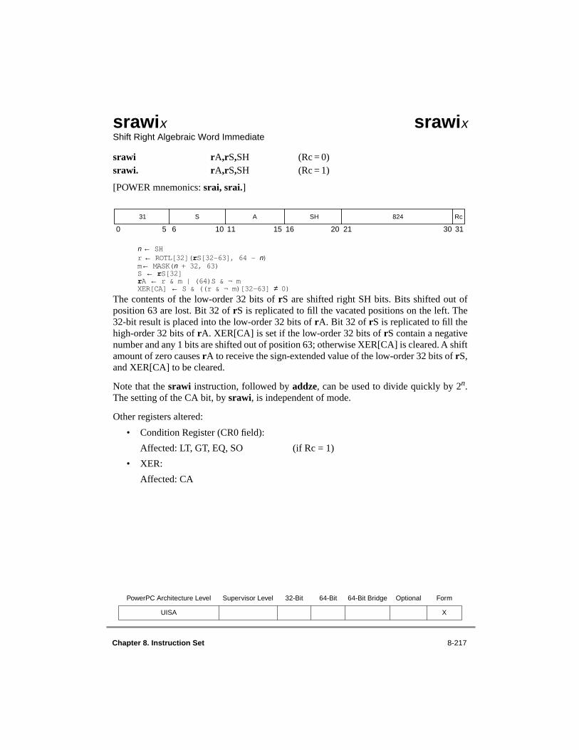
Chapter 8. Instruction Set 8-217
srawix srawix Shift Right Algebraic Word Immediate
srawi rA,rS,SH (Rc = 0) srawi. rA,rS,SH (Rc = 1)
[POWER mnemonics: srai, srai.]
n ← SHr ← ROTL[32](rS[32–63], 64 – n)m← MASK(n + 32, 63)S ← rS[32]rA ← r & m | (64)S & ¬ mXER[CA] ← S & ((r & ¬ m)[32–63] ≠ 0)
The contents of the low-order 32 bits of rS are shifted right SH bits. Bits shifted out ofposition 63 are lost. Bit 32 of rS is replicated to fill the vacated positions on the left. The32-bit result is placed into the low-order 32 bits of rA. Bit 32 of rS is replicated to fill thehigh-order 32 bits of rA. XER[CA] is set if the low-order 32 bits of rS contain a negativenumber and any 1 bits are shifted out of position 63; otherwise XER[CA] is cleared. A shiftamount of zero causes rA to receive the sign-extended value of the low-order 32 bits of rS,and XER[CA] to be cleared.
Note that the srawi instruction, followed by addze, can be used to divide quickly by 2n.The setting of the CA bit, by srawi, is independent of mode.
Other registers altered:
• Condition Register (CR0 field):
Affected: LT, GT, EQ, SO (if Rc = 1)
• XER:
Affected: CA
PowerPC Architecture Level Supervisor Level 32-Bit 64-Bit 64-Bit Bridge Optional Form
UISA X
0 5 6 10 11 15 16 20 21 30 31
31 S A SH 824 Rc

8-218 PowerPC Microprocessor Family: The Programming Environments, Rev. 1
srdx 64-Bit Implementations Only srdxShift Right Double Word
srd rA,rS,rB (Rc = 0)srd. rA,rS,rB (Rc = 1)
n ← rB[58–63]r ← ROTL[64](rS, 64 – n)if rB[57] = 0 then
m ← MASK(n, 63)else m ← (64)0rA ← r & m
The contents of rS are shifted right the number of bits specified by the low-order seven bitsof rB. Bits shifted out of position 63 are lost. Zeros are supplied to the vacated positions onthe left. The result is placed into rA. Shift amounts from 64 to 127 give a zero result.
This instruction is defined only for 64-bit implementations. Using it on a 32-bitimplementation will cause the system illegal instruction error handler to be invoked.
Other registers altered:
• Condition Register (CR0 field):
Affected: LT, GT, EQ, SO (if Rc = 1)
PowerPC Architecture Level Supervisor Level 32-Bit 64-Bit 64-Bit Bridge Optional Form
UISA √ X
0 5 6 10 11 15 16 20 21 30 31
31 S A B 539 Rc
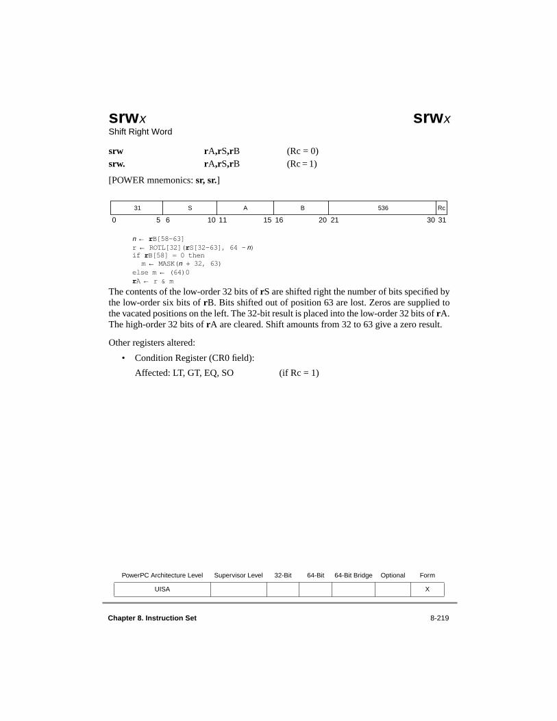
Chapter 8. Instruction Set 8-219
srwx srwx Shift Right Word
srw rA,rS,rB (Rc = 0)srw. rA,rS,rB (Rc = 1)
[POWER mnemonics: sr, sr.]
n ← rB[58–63]r ← ROTL[32](rS[32–63], 64 – n)if rB[58] = 0 then
m ← MASK(n + 32, 63)else m ← (64)0rA ← r & m
The contents of the low-order 32 bits of rS are shifted right the number of bits specified bythe low-order six bits of rB. Bits shifted out of position 63 are lost. Zeros are supplied tothe vacated positions on the left. The 32-bit result is placed into the low-order 32 bits of rA.The high-order 32 bits of rA are cleared. Shift amounts from 32 to 63 give a zero result.
Other registers altered:
• Condition Register (CR0 field):
Affected: LT, GT, EQ, SO (if Rc = 1)
PowerPC Architecture Level Supervisor Level 32-Bit 64-Bit 64-Bit Bridge Optional Form
UISA X
0 5 6 10 11 15 16 20 21 30 31
31 S A B 536 Rc

8-220 PowerPC Microprocessor Family: The Programming Environments, Rev. 1
stb stbStore Byte
stb rS,d(rA)
if rA = 0 then b ← 0else b ← (rA)EA ← b + EXTS(d)MEM(EA, 1) ← rS[56–63]
EA is the sum (rA|0) + d. The contents of the low-order eight bits of rS are stored into thebyte in memory addressed by EA.
Other registers altered:
• None
PowerPC Architecture Level Supervisor Level 32-Bit 64-Bit 64-Bit Bridge Optional Form
UISA D
0 5 6 10 11 15 16 31
38 S A d

Chapter 8. Instruction Set 8-221
stbu stbuStore Byte with Update
stbu rS,d(rA)
EA ← (rA) + EXTS(d)MEM(EA, 1) ← rS[56–63]rA ← EA
EA is the sum (rA) + d. The contents of the low-order eight bits of rS are stored into thebyte in memory addressed by EA.
EA is placed into rA.
If rA = 0, the instruction form is invalid.
Other registers altered:
• None
PowerPC Architecture Level Supervisor Level 32-Bit 64-Bit 64-Bit Bridge Optional Form
UISA D
0 5 6 10 11 15 16 31
39 S A d

8-222 PowerPC Microprocessor Family: The Programming Environments, Rev. 1
stbux stbuxStore Byte with Update Indexed
stbux rS,rA,rB
EA ← (rA) + (rB)MEM(EA, 1) ← rS[56–63]rA ← EA
EA is the sum (rA) + (rB). The contents of the low-order eight bits of rS are stored into thebyte in memory addressed by EA.
EA is placed into rA.
If rA = 0, the instruction form is invalid.
Other registers altered:
• None
PowerPC Architecture Level Supervisor Level 32-Bit 64-Bit 64-Bit Bridge Optional Form
UISA X
Reserved
0 5 6 10 11 15 16 21 22 30 31
31 S A B 247 0

Chapter 8. Instruction Set 8-223
stbx stbxStore Byte Indexed
stbx rS,rA,rB
if rA = 0 then b ← 0else b ← (rA)EA ← b + (rB)MEM(EA, 1) ← rS[56–63]
EA is the sum (rA|0) + (rB). The contents of the low-order eight bits of rS are stored intothe byte in memory addressed by EA.
Other registers altered:
• None
PowerPC Architecture Level Supervisor Level 32-Bit 64-Bit 64-Bit Bridge Optional Form
UISA X
Reserved
0 5 6 10 11 15 16 21 22 30 31
31 S A B 215 0
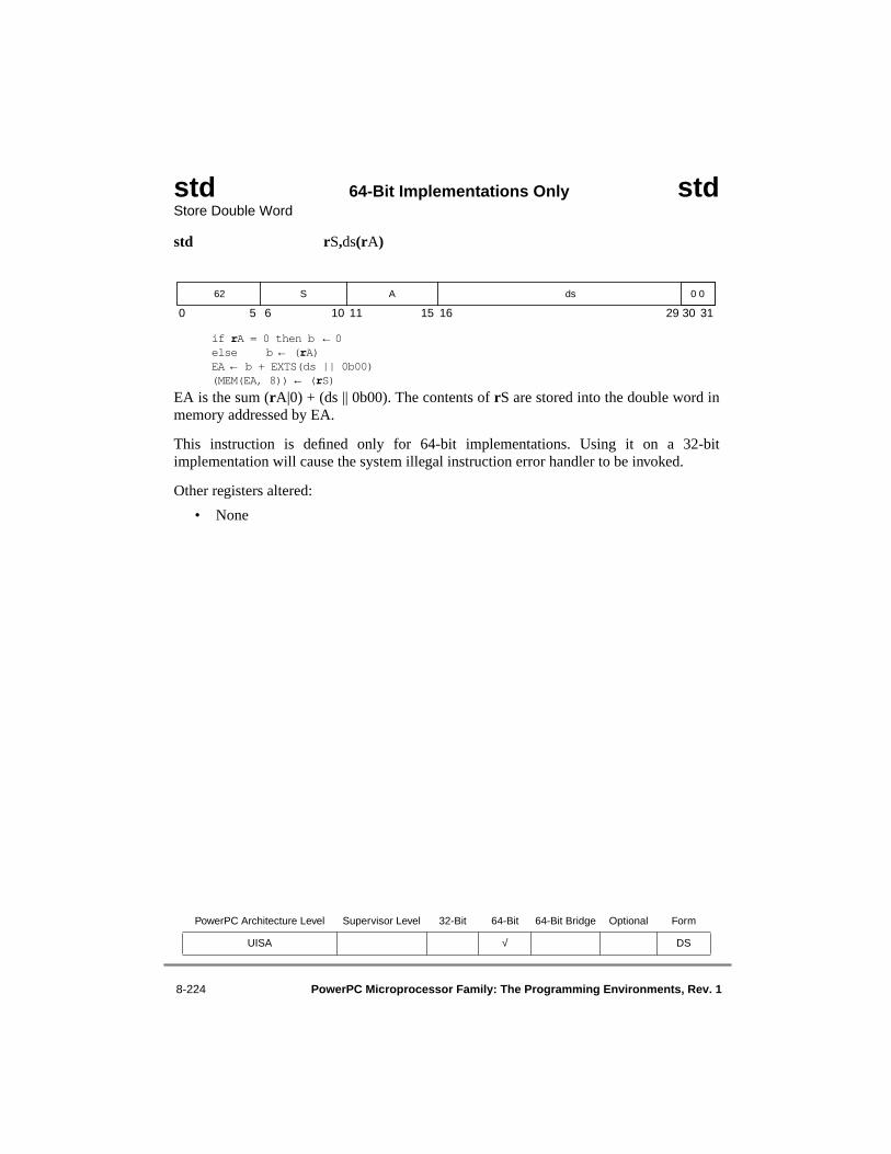
8-224 PowerPC Microprocessor Family: The Programming Environments, Rev. 1
std 64-Bit Implementations Only stdStore Double Word
std rS,ds(rA)
if rA = 0 then b ← 0else b ← (rA)EA ← b + EXTS(ds || 0b00)(MEM(EA, 8)) ← (rS)
EA is the sum (rA|0) + (ds || 0b00). The contents of rS are stored into the double word inmemory addressed by EA.
This instruction is defined only for 64-bit implementations. Using it on a 32-bitimplementation will cause the system illegal instruction error handler to be invoked.
Other registers altered:
• None
PowerPC Architecture Level Supervisor Level 32-Bit 64-Bit 64-Bit Bridge Optional Form
UISA √ DS
0 5 6 10 11 15 16 29 30 31
62 S A ds 0 0
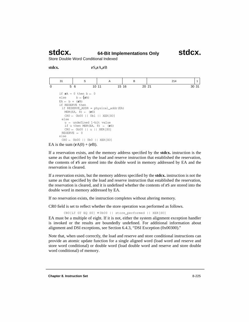
Chapter 8. Instruction Set 8-225
stdcx. 64-Bit Implementations Only stdcx.Store Double Word Conditional Indexed
stdcx. rS,rA,rB
if rA = 0 then b ← 0else b ← (rA)EA ← b + (rB)if RESERVE thenif RESERVE_ADDR = physical_addr(EA)MEM(EA, 8) ← (rS)CR0 ← 0b00 || 0b1 || XER[SO]
elseu ← undefined 1-bit valueif u then MEM(EA, 8) ← (rS)CR0 ← 0b00 || u || XER[SO]
RESERVE ← 0elseCR0 ← 0b00 || 0b0 || XER[SO]
EA is the sum (rA|0) + (rB).
If a reservation exists, and the memory address specified by the stdcx. instruction is thesame as that specified by the load and reserve instruction that established the reservation,the contents of rS are stored into the double word in memory addressed by EA and thereservation is cleared.
If a reservation exists, but the memory address specified by the stdcx. instruction is not thesame as that specified by the load and reserve instruction that established the reservation,the reservation is cleared, and it is undefined whether the contents of rS are stored into thedouble word in memory addressed by EA.
If no reservation exists, the instruction completes without altering memory.
CR0 field is set to reflect whether the store operation was performed as follows.
CR0[LT GT EQ S0] = 0b00 || store_performed || XER[SO]
EA must be a multiple of eight. If it is not, either the system alignment exception handleris invoked or the results are boundedly undefined. For additional information aboutalignment and DSI exceptions, see Section 6.4.3, “DSI Exception (0x00300).”
Note that, when used correctly, the load and reserve and store conditional instructions canprovide an atomic update function for a single aligned word (load word and reserve andstore word conditional) or double word (load double word and reserve and store doubleword conditional) of memory.
0 5 6 10 11 15 16 20 21 30 31
31 S A B 214 1

8-226 PowerPC Microprocessor Family: The Programming Environments, Rev. 1
In general, correct use requires that load word and reserve be paired with store wordconditional, and load double word and reserve with store double word conditional, with thesame memory address specified by both instructions of the pair. The only exception is thatan unpaired store word conditional or store double word conditional instruction to any(scratch) EA can be used to clear any reservation held by the processor. Examples of correctuses of these instructions, to emulate primitives such as fetch and add, test and set, andcompare and swap can be found in Appendix E, “Synchronization ProgrammingExamples.”
A reservation is cleared if any of the following events occurs:
• The processor holding the reservation executes another load and reserve instruction; this clears the first reservation and establishes a new one.
• The processor holding the reservation executes a store conditional instruction to any address.
• Another processor executes any store instruction to the address associated with the reservation.]
• Any mechanism, other than the processor holding the reservation, stores to the address associated with the reservation.
This instruction is defined only for 64-bit implementations. Using it on a 32-bitimplementation will cause the system illegal instruction error handler to be invoked.
Other registers altered:
• Condition Register (CR0 field):
Affected: LT, GT, EQ, SO
PowerPC Architecture Level Supervisor Level 32-Bit 64-Bit 64-Bit Bridge Optional Form
UISA √ X
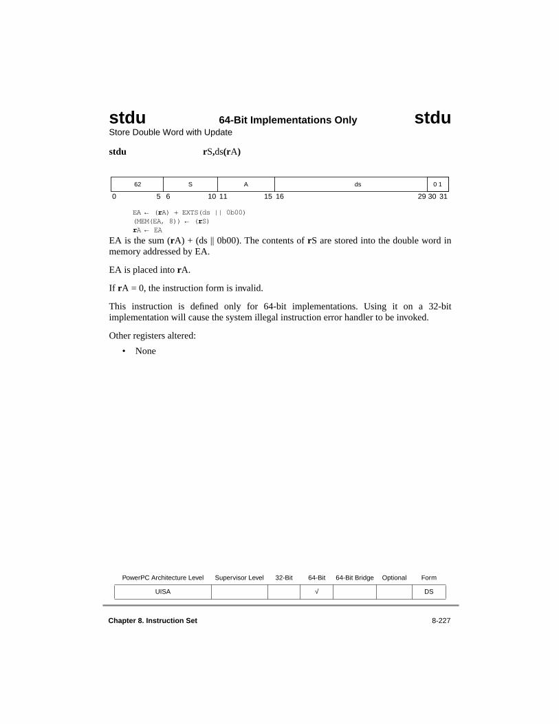
Chapter 8. Instruction Set 8-227
stdu 64-Bit Implementations Only stduStore Double Word with Update
stdu rS,ds(rA)
EA ← (rA) + EXTS(ds || 0b00)(MEM(EA, 8)) ← (rS)rA ← EA
EA is the sum (rA) + (ds || 0b00). The contents of rS are stored into the double word inmemory addressed by EA.
EA is placed into rA.
If rA = 0, the instruction form is invalid.
This instruction is defined only for 64-bit implementations. Using it on a 32-bitimplementation will cause the system illegal instruction error handler to be invoked.
Other registers altered:
• None
PowerPC Architecture Level Supervisor Level 32-Bit 64-Bit 64-Bit Bridge Optional Form
UISA √ DS
0 5 6 10 11 15 16 29 30 31
62 S A ds 0 1
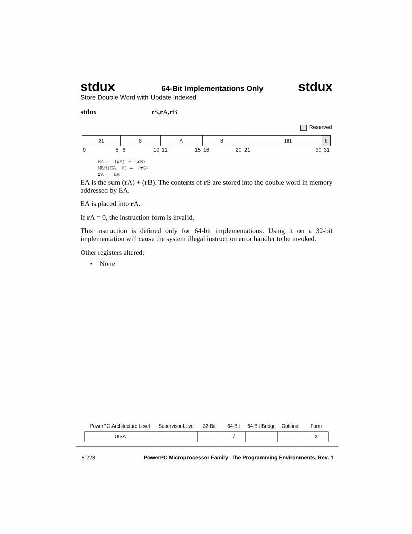
8-228 PowerPC Microprocessor Family: The Programming Environments, Rev. 1
stdux 64-Bit Implementations Only stduxStore Double Word with Update Indexed
stdux rS,rA,rB
EA ← (rA) + (rB)MEM(EA, 8) ← (rS)rA ← EA
EA is the sum (rA) + (rB). The contents of rS are stored into the double word in memoryaddressed by EA.
EA is placed into rA.
If rA = 0, the instruction form is invalid.
This instruction is defined only for 64-bit implementations. Using it on a 32-bitimplementation will cause the system illegal instruction error handler to be invoked.
Other registers altered:
• None
PowerPC Architecture Level Supervisor Level 32-Bit 64-Bit 64-Bit Bridge Optional Form
UISA √ X
0 5 6 10 11 15 16 20 21 30 31
Reserved
31 S A B 181 0
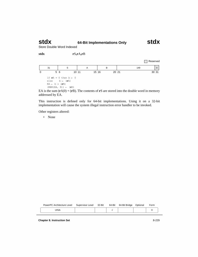
Chapter 8. Instruction Set 8-229
stdx 64-Bit Implementations Only stdxStore Double Word Indexed
stdx rS,rA,rB
if rA = 0 then b ← 0else b ← (rA)EA ← b + (rB)(MEM(EA, 8)) ← (rS)
EA is the sum (rA|0) + (rB). The contents of rS are stored into the double word in memoryaddressed by EA.
This instruction is defined only for 64-bit implementations. Using it on a 32-bitimplementation will cause the system illegal instruction error handler to be invoked.
Other registers altered:
• None
PowerPC Architecture Level Supervisor Level 32-Bit 64-Bit 64-Bit Bridge Optional Form
UISA √ X
0 5 6 10 11 15 16 20 21 30 31
Reserved
31 S A B 149 0
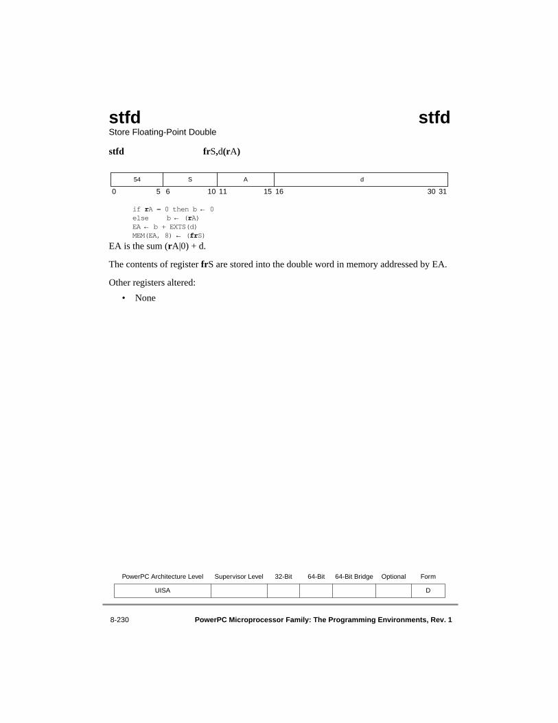
8-230 PowerPC Microprocessor Family: The Programming Environments, Rev. 1
stfd stfdStore Floating-Point Double
stfd frS,d(rA)
if rA = 0 then b ← 0else b ← (rA)EA ← b + EXTS(d)MEM(EA, 8) ← (frS)
EA is the sum (rA|0) + d.
The contents of register frS are stored into the double word in memory addressed by EA.
Other registers altered:
• None
PowerPC Architecture Level Supervisor Level 32-Bit 64-Bit 64-Bit Bridge Optional Form
UISA D
0 5 6 10 11 15 16 30 31
54 S A d

Chapter 8. Instruction Set 8-231
stfdu stfduStore Floating-Point Double with Update
stfdu frS,d(rA)
EA ← (rA) + EXTS(d)MEM(EA, 8) ← (frS)rA ← EA
EA is the sum (rA) + d.
The contents of register frS are stored into the double word in memory addressed by EA.
EA is placed into rA.
If rA = 0, the instruction form is invalid.
Other registers altered:
• None
PowerPC Architecture Level Supervisor Level 32-Bit 64-Bit 64-Bit Bridge Optional Form
UISA D
0 5 6 10 11 15 16 31
55 S A d
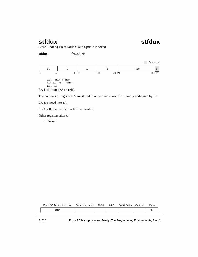
8-232 PowerPC Microprocessor Family: The Programming Environments, Rev. 1
stfdux stfduxStore Floating-Point Double with Update Indexed
stfdux frS,rA,rB
EA ← (rA) + (rB)MEM(EA, 8) ← (frS)rA ← EA
EA is the sum (rA) + (rB).
The contents of register frS are stored into the double word in memory addressed by EA.
EA is placed into rA.
If rA = 0, the instruction form is invalid.
Other registers altered:
• None
PowerPC Architecture Level Supervisor Level 32-Bit 64-Bit 64-Bit Bridge Optional Form
UISA X
Reserved
0 5 6 10 11 15 16 20 21 30 31
31 S A B 759 0
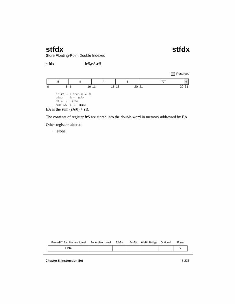
Chapter 8. Instruction Set 8-233
stfdx stfdxStore Floating-Point Double Indexed
stfdx frS,rA,rB
if rA = 0 then b ← 0else b ← (rA)EA ← b + (rB)MEM(EA, 8) ← (frS)
EA is the sum (rA|0) + rB.
The contents of register frS are stored into the double word in memory addressed by EA.
Other registers altered:
• None
PowerPC Architecture Level Supervisor Level 32-Bit 64-Bit 64-Bit Bridge Optional Form
UISA X
Reserved
0 5 6 10 11 15 16 20 21 30 31
31 S A B 727 0

8-234 PowerPC Microprocessor Family: The Programming Environments, Rev. 1
stfiwx stfiwxStore Floating-Point as Integer Word Indexed
stfiwx frS,rA,rB
if rA = 0 then b ← 0else b ← (rA)EA ← b + (rB)MEM(EA, 4) ← frS[32–63]
EA is the sum (rA|0) + (rB).
The contents of the low-order 32 bits of register frS are stored, without conversion, into theword in memory addressed by EA.
If the contents of register frS were produced, either directly or indirectly, by an lfsinstruction, a single-precision arithmetic instruction, or frsp, then the value stored isundefined. The contents of frS are produced directly by such an instruction if frS is thetarget register for the instruction. The contents of frS are produced indirectly by such aninstruction if frS is the final target register of a sequence of one or more floating-point moveinstructions, with the input to the sequence having been produced directly by such aninstruction.
This instruction is defined as optional by the PowerPC architecture to ensure backwardscompatibility with earlier processors; however, it will likely be required for subsequentPowerPC processors.
Other registers altered:
• None
PowerPC Architecture Level Supervisor Level 32-Bit 64-Bit 64-Bit Bridge Optional Form
UISA √ X
0 5 6 10 11 15 16 20 21 30 31
Reserved
31 S A B 983 0
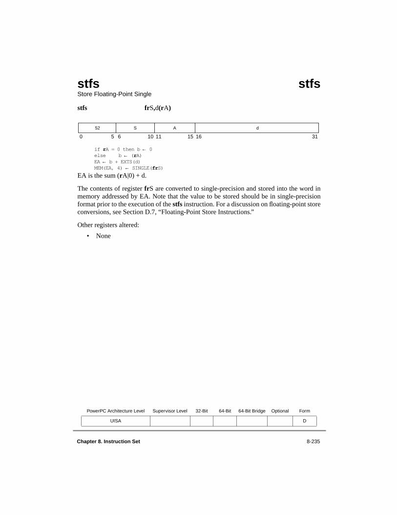
Chapter 8. Instruction Set 8-235
stfs stfs Store Floating-Point Single
stfs frS,d(rA)
if rA = 0 then b ← 0else b ← (rA)EA ← b + EXTS(d)MEM(EA, 4) ← SINGLE(frS)
EA is the sum (rA|0) + d.
The contents of register frS are converted to single-precision and stored into the word inmemory addressed by EA. Note that the value to be stored should be in single-precisionformat prior to the execution of the stfs instruction. For a discussion on floating-point storeconversions, see Section D.7, “Floating-Point Store Instructions.”
Other registers altered:
• None
PowerPC Architecture Level Supervisor Level 32-Bit 64-Bit 64-Bit Bridge Optional Form
UISA D
0 5 6 10 11 15 16 31
52 S A d
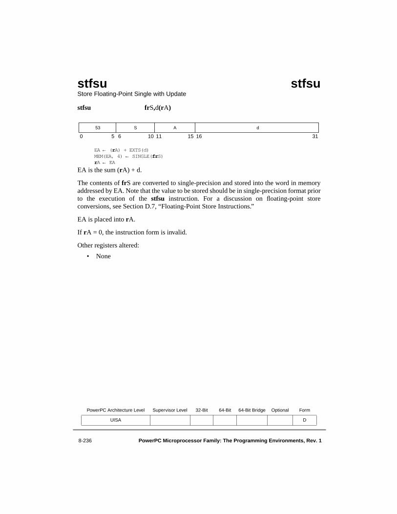
8-236 PowerPC Microprocessor Family: The Programming Environments, Rev. 1
stfsu stfsu Store Floating-Point Single with Update
stfsu frS,d(rA)
EA ← (rA) + EXTS(d)MEM(EA, 4) ← SINGLE(frS)rA ← EA
EA is the sum (rA) + d.
The contents of frS are converted to single-precision and stored into the word in memoryaddressed by EA. Note that the value to be stored should be in single-precision format priorto the execution of the stfsu instruction. For a discussion on floating-point storeconversions, see Section D.7, “Floating-Point Store Instructions.”
EA is placed into rA.
If rA = 0, the instruction form is invalid.
Other registers altered:
• None
PowerPC Architecture Level Supervisor Level 32-Bit 64-Bit 64-Bit Bridge Optional Form
UISA D
0 5 6 10 11 15 16 31
53 S A d

Chapter 8. Instruction Set 8-237
stfsux stfsux Store Floating-Point Single with Update Indexed
stfsux frS,rA,rB
EA ← (rA) + (rB)MEM(EA, 4) ← SINGLE(frS)rA ← EA
EA is the sum (rA) + (rB).
The contents of frS are converted to single-precision and stored into the word in memoryaddressed by EA. For a discussion on floating-point store conversions, see Section D.7,“Floating-Point Store Instructions.”
EA is placed into rA.
If rA = 0, the instruction form is invalid.
Other registers altered:
• None
PowerPC Architecture Level Supervisor Level 32-Bit 64-Bit 64-Bit Bridge Optional Form
UISA X
Reserved
0 5 6 10 11 15 16 20 21 30 31
31 S A B 695 0

8-238 PowerPC Microprocessor Family: The Programming Environments, Rev. 1
stfsx stfsx Store Floating-Point Single Indexed
stfsx frS,rA,rB
if rA = 0 then b ← 0else b ← (rA)EA ← b + (rB)MEM(EA, 4) ← SINGLE(frS)
EA is the sum (rA|0) + (rB).
The contents of register frS are converted to single-precision and stored into the word inmemory addressed by EA. For a discussion on floating-point store conversions, seeSection D.7, “Floating-Point Store Instructions.”
Other registers altered:
• None
PowerPC Architecture Level Supervisor Level 32-Bit 64-Bit 64-Bit Bridge Optional Form
UISA X
Reserved
0 5 6 10 11 15 16 20 21 30 31
31 S A B 663 0
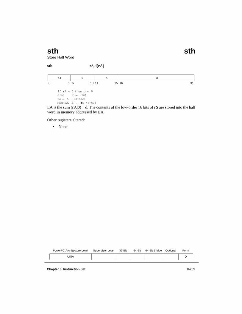
Chapter 8. Instruction Set 8-239
sth sthStore Half Word
sth rS,d(rA)
if rA = 0 then b ← 0else b ← (rA)EA ← b + EXTS(d)MEM(EA, 2) ← rS[48–63]
EA is the sum (rA|0) + d. The contents of the low-order 16 bits of rS are stored into the halfword in memory addressed by EA.
Other registers altered:
• None
PowerPC Architecture Level Supervisor Level 32-Bit 64-Bit 64-Bit Bridge Optional Form
UISA D
0 5 6 10 11 15 16 31
44 S A d

8-240 PowerPC Microprocessor Family: The Programming Environments, Rev. 1
sthbrx sthbrxStore Half Word Byte-Reverse Indexed
sthbrx rS,rA,rB
if rA = 0 then b ← 0else b ← (rA)EA ← b + (rB)MEM(EA, 2) ← rS[56–63] || rS[48–55]
EA is the sum (rA|0) + (rB). The contents of the low-order eight bits of rS are stored intobits 0–7 of the half word in memory addressed by EA. The contents of the subsequent low-order eight bits of rS are stored into bits 8–15 of the half word in memory addressed by EA.
Other registers altered:
• None
PowerPC Architecture Level Supervisor Level 32-Bit 64-Bit 64-Bit Bridge Optional Form
UISA X
Reserved
0 5 6 10 11 15 16 20 21 30 31
31 S A B 918 0

Chapter 8. Instruction Set 8-241
sthu sthuStore Half Word with Update
sthu rS,d(rA)
EA ← (rA) + EXTS(d)MEM(EA, 2) ← rS[48–63]rA ← EA
EA is the sum (rA) + d. The contents of the low-order 16 bits of rS are stored into the halfword in memory addressed by EA.
EA is placed into rA.
If rA = 0, the instruction form is invalid.
Other registers altered:
• None
PowerPC Architecture Level Supervisor Level 32-Bit 64-Bit 64-Bit Bridge Optional Form
UISA D
0 5 6 10 11 15 16 31
45 S A d

8-242 PowerPC Microprocessor Family: The Programming Environments, Rev. 1
sthux sthuxStore Half Word with Update Indexed
sthux rS,rA,rB
EA ← (rA) + (rB)MEM(EA, 2) ← rS[48–63]rA ← EA
EA is the sum (rA) + (rB). The contents of the low-order 16 bits of rS are stored into thehalf word in memory addressed by EA.
EA is placed into rA.
If rA = 0, the instruction form is invalid.
Other registers altered:
• None
PowerPC Architecture Level Supervisor Level 32-Bit 64-Bit 64-Bit Bridge Optional Form
UISA X
Reserved
0 5 6 10 11 15 16 20 21 30 31
31 S A B 439 0
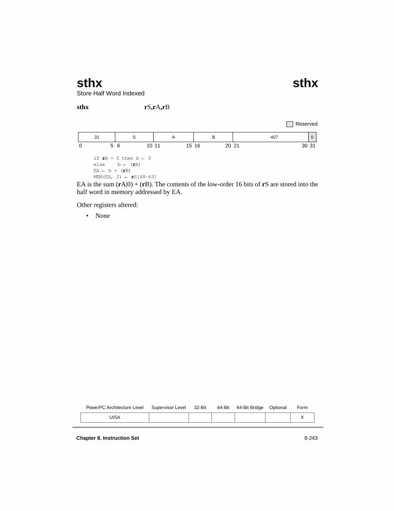
Chapter 8. Instruction Set 8-243
sthx sthxStore Half Word Indexed
sthx rS,rA,rB
if rA = 0 then b ← 0else b ← (rA)EA ← b + (rB)MEM(EA, 2) ← rS[48–63]
EA is the sum (rA|0) + (rB). The contents of the low-order 16 bits of rS are stored into thehalf word in memory addressed by EA.
Other registers altered:
• None
PowerPC Architecture Level Supervisor Level 32-Bit 64-Bit 64-Bit Bridge Optional Form
UISA X
Reserved
0 5 6 10 11 15 16 20 21 30 31
31 S A B 407 0

8-244 PowerPC Microprocessor Family: The Programming Environments, Rev. 1
stmw stmwStore Multiple Word
stmw rS,d(rA)
[POWER mnemonic: stm]
if rA = 0 then b ← 0else b ← (rA)EA ← b + EXTS(d)r ← rSdo while r ≤ 31
MEM(EA, 4) ← GPR(r)[32–63]r ← r + 1EA ← EA + 4
EA is the sum (rA|0) + d.
n = (32 – rS).
n consecutive words starting at EA are stored from the low-order 32 bits of GPRs rSthrough r31. For example, if rS = 30, 2 words are stored.
EA must be a multiple of four. If it is not, either the system alignment exception handler isinvoked or the results are boundedly undefined. For additional information about alignmentand DSI exceptions, see Section 6.4.3, “DSI Exception (0x00300).”
Note that, in some implementations, this instruction is likely to have a greater latency andtake longer to execute, perhaps much longer, than a sequence of individual load or storeinstructions that produce the same results.
Other registers altered:
• None
PowerPC Architecture Level Supervisor Level 32-Bit 64-Bit 64-Bit Bridge Optional Form
UISA D
0 5 6 10 11 15 16 31
47 S A d

Chapter 8. Instruction Set 8-245
stswi stswiStore String Word Immediate
stswi rS,rA,NB
[POWER mnemonic: stsi]
if rA = 0 then EA ← 0else EA ← (rA)if NB = 0 then n ← 32else n ← NBr ← rS – 1i ← 32do while n > 0
if i = 32 then r ← r + 1 (mod 32)MEM(EA, 1) ← GPR(r)[i–i + 7]i ← i + 8if i = 64 then i ← 32EA ← EA + 1n ← n – 1
EA is (rA|0). Let n = NB if NB ≠ 0, n = 32 if NB = 0; n is the number of bytes to store. Letnr = CEIL(n ÷ 4); nr is the number of registers to supply data.
n consecutive bytes starting at EA are stored from GPRs rS through rS + nr – 1. Data isstored from the low-order four bytes of each GPR. Bytes are stored left to right from eachregister. The sequence of registers wraps around through r0 if required.
Under certain conditions (for example, segment boundary crossing) the data alignmentexception handler may be invoked. For additional information about data alignmentexceptions, see Section 6.4.3, “DSI Exception (0x00300).”
Note that, in some implementations, this instruction is likely to have a greater latency andtake longer to execute, perhaps much longer, than a sequence of individual load or storeinstructions that produce the same results.
Other registers altered:
• None
PowerPC Architecture Level Supervisor Level 32-Bit 64-Bit 64-Bit Bridge Optional Form
UISA X
Reserved
0 5 6 10 11 15 16 20 21 30 31
31 S A NB 725 0

8-246 PowerPC Microprocessor Family: The Programming Environments, Rev. 1
stswx stswxStore String Word Indexed
stswx rS,rA,rB
[POWER mnemonic: stsx]
if rA = 0 then b ← 0else b ← (rA)EA ← b + (rB)n ← XER[25–31]r ← rS – 1i ← 32do while n > 0
if i = 32 then r ← r + 1 (mod 32)MEM(EA, 1) ← GPR(r)[i–i + 7]i ← i + 8if i = 64 then i ← 32EA ← EA + 1n ← n – 1
EA is the sum (rA|0) + (rB). Let n = XER[25–31]; n is the number of bytes to store. Let nr = CEIL(n ÷ 4); nr is the number of registers to supply data.
n consecutive bytes starting at EA are stored from GPRs rS through rS + nr – 1. Data isstored from the low-order four bytes of each GPR. Bytes are stored left to right from eachregister. The sequence of registers wraps around through r0 if required. If n = 0, no bytesare stored.
Under certain conditions (for example, segment boundary crossing) the data alignmentexception handler may be invoked. For additional information about data alignmentexceptions, see Section 6.4.3, “DSI Exception (0x00300).”
Note that, in some implementations, this instruction is likely to have a greater latency andtake longer to execute, perhaps much longer, than a sequence of individual load or storeinstructions that produce the same results.
Other registers altered:
• None
PowerPC Architecture Level Supervisor Level 32-Bit 64-Bit 64-Bit Bridge Optional Form
UISA X
Reserved
0 5 6 10 11 15 16 20 21 30 31
31 S A B 661 0
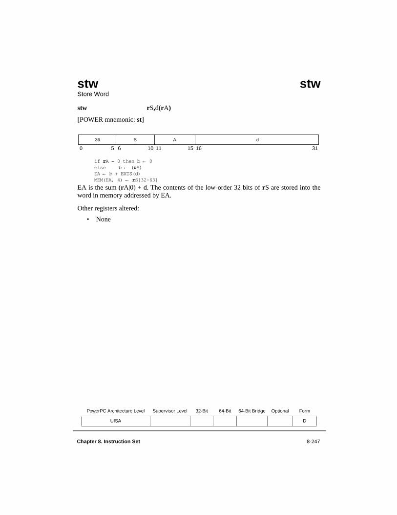
Chapter 8. Instruction Set 8-247
stw stwStore Word
stw rS,d(rA)
[POWER mnemonic: st]
if rA = 0 then b ← 0else b ← (rA)EA ← b + EXTS(d)MEM(EA, 4) ← rS[32–63]
EA is the sum (rA|0) + d. The contents of the low-order 32 bits of rS are stored into theword in memory addressed by EA.
Other registers altered:
• None
PowerPC Architecture Level Supervisor Level 32-Bit 64-Bit 64-Bit Bridge Optional Form
UISA D
0 5 6 10 11 15 16 31
36 S A d

8-248 PowerPC Microprocessor Family: The Programming Environments, Rev. 1
stwbrx stwbrxStore Word Byte-Reverse Indexed
stwbrx rS,rA,rB
[POWER mnemonic: stbrx]
if rA = 0 then b ← 0else b ← (rA)EA ← b + (rB) MEM(EA, 4) ← rS[56–63] || rS[48–55] || rS[40–47] || rS[32–39]
EA is the sum (rA|0) + (rB). The contents of the low-order eight bits of rS are stored intobits 0–7 of the word in memory addressed by EA. The contents of the subsequent eight low-order bits of rS are stored into bits 8–15 of the word in memory addressed by EA. Thecontents of the subsequent eight low-order bits of rS are stored into bits 16–23 of the wordin memory addressed by EA. The contents of the subsequent eight low-order bits of rS arestored into bits 24–31 of the word in memory addressed by EA.
Other registers altered:
• None
PowerPC Architecture Level Supervisor Level 32-Bit 64-Bit 64-Bit Bridge Optional Form
UISA X
Reserved
0 5 6 10 11 15 16 20 21 30 31
31 S A B 662 0

Chapter 8. Instruction Set 8-249
stwcx. stwcx.Store Word Conditional Indexed
stwcx. rS,rA,rB
if rA = 0 then b ← 0else b ← (rA)EA ← b + (rB)if RESERVE thenif RESERVE_ADDR = physical_addr(EA)MEM(EA, 4) ← rS[32–63]CR0 ← 0b00 || 0b1 || XER[SO]
elseu ← undefined 1-bit valueif u then MEM(EA, 4) ← rS[32–63]CR0 ← 0b00 || u || XER[SO]
RESERVE ← 0elseCR0 ← 0b00 || 0b0 || XER[SO]
EA is the sum (rA|0) + (rB). If the reserved bit is set, the stwcx. instruction stores rS toeffective address (rA + rB), clears the reserved bit, and sets CR0[EQ]. If the reserved bitis not set, the stwcx. instruction does not do a store; it leaves the reserved bit cleared andclears CR0[EQ]. Software must look at CR0[EQ] to see if the stwcx. was successful.
The reserved bit is set by the lwarx instruction. The reserved bit is cleared by any stwcx.instruction to any address, and also by snooping logic if it detects that another processordoes any kind of store to the block indicated in the reservation buffer when reserved is set.
If a reservation exists, and the memory address specified by the stwcx. instruction is thesame as that specified by the load and reserve instruction that established the reservation,the contents of the low-order 32 bits of rS are stored into the word in memory addressed byEA and the reservation is cleared.
If a reservation exists, but the memory address specified by the stwcx. instruction is not thesame as that specified by the load and reserve instruction that established the reservation,the reservation is cleared, and it is undefined whether the contents of the low-order 32 bitsof rS are stored into the word in memory addressed by EA.
If no reservation exists, the instruction completes without altering memory.
CR0 field is set to reflect whether the store operation was performed as follows.
CR0[LT GT EQ S0] = 0b00 || store_performed || XER[SO]
EA must be a multiple of four. If it is not, either the system alignment exception handler isinvoked or the results are boundedly undefined. For additional information about alignmentand DSI exceptions, see Section 6.4.3, “DSI Exception (0x00300).”
0 5 6 10 11 15 16 20 21 30 31
31 S A B 150 1
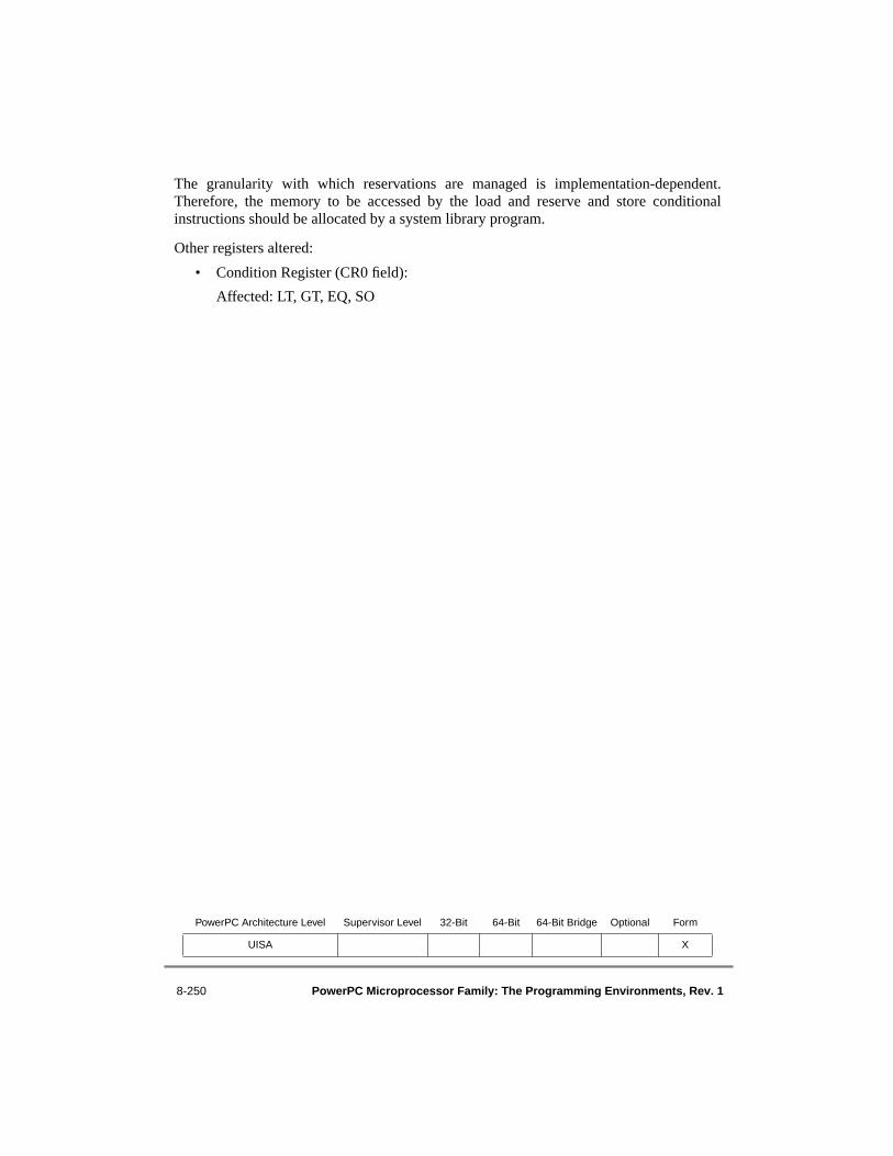
8-250 PowerPC Microprocessor Family: The Programming Environments, Rev. 1
The granularity with which reservations are managed is implementation-dependent.Therefore, the memory to be accessed by the load and reserve and store conditionalinstructions should be allocated by a system library program.
Other registers altered:
• Condition Register (CR0 field):
Affected: LT, GT, EQ, SO
PowerPC Architecture Level Supervisor Level 32-Bit 64-Bit 64-Bit Bridge Optional Form
UISA X

Chapter 8. Instruction Set 8-251
stwu stwuStore Word with Update
stwu rS,d(rA)
[POWER mnemonic: stu]
EA ← (rA) + EXTS(d)MEM(EA, 4) ← rS[32–63]rA ← EA
EA is the sum (rA) + d. The contents of the low-order 32 bits of rS are stored into the wordin memory addressed by EA.
EA is placed into rA.
If rA = 0, the instruction form is invalid.
Other registers altered:
• None
PowerPC Architecture Level Supervisor Level 32-Bit 64-Bit 64-Bit Bridge Optional Form
UISA D
0 5 6 10 11 15 16 31
37 S A d

8-252 PowerPC Microprocessor Family: The Programming Environments, Rev. 1
stwux stwuxStore Word with Update Indexed
stwux rS,rA,rB
[POWER mnemonic: stux]
EA ← (rA) + (rB)MEM(EA, 4) ← rS[32–63]rA ← EA
EA is the sum (rA) + (rB). The contents of the low-order 32 bits of rS are stored into theword in memory addressed by EA.
EA is placed into rA.
If rA = 0, the instruction form is invalid.
Other registers altered:
• None
PowerPC Architecture Level Supervisor Level 32-Bit 64-Bit 64-Bit Bridge Optional Form
UISA X
Reserved
0 5 6 10 11 15 16 20 21 30 31
31 S A B 183 0

Chapter 8. Instruction Set 8-253
stwx stwxStore Word Indexed
stwx rS,rA,rB
[POWER mnemonic: stx]
if rA = 0 then b ← 0else b ← (rA)EA ← b + (rB)MEM(EA, 4) ← rS[32–63]
EA is the sum (rA|0) + (rB). The contents of the low-order 32 bits of rS are is stored intothe word in memory addressed by EA.
Other registers altered:
• None
PowerPC Architecture Level Supervisor Level 32-Bit 64-Bit 64-Bit Bridge Optional Form
UISA X
Reserved
0 5 6 10 11 15 16 20 21 30 31
31 S A B 151 0

8-254 PowerPC Microprocessor Family: The Programming Environments, Rev. 1
subfx subfxSubtract From
subf rD,rA,rB (OE = 0 Rc = 0)subf. rD,rA,rB (OE = 0 Rc = 1) subfo rD,rA,rB (OE = 1 Rc = 0) subfo. rD,rA,rB (OE = 1 Rc = 1)
rD ← ¬ (rA) + (rB) + 1The sum ¬ (rA) + (rB) + 1 is placed into rD.
The subf instruction is preferred for subtraction because it sets few status bits.
Other registers altered:
• Condition Register (CR0 field):
Affected: LT, GT, EQ, SO (if Rc = 1)
• XER:
Affected: SO, OV (if OE = 1)
Simplified mnemonics:
sub rD,rA,rB equivalent to subf rD,rB,rA
PowerPC Architecture Level Supervisor Level 32-Bit 64-Bit 64-Bit Bridge Optional Form
UISA XO
0 5 6 10 11 15 16 20 21 22 30 31
31 D A B OE 40 Rc

Chapter 8. Instruction Set 8-255
subfcx subfcx Subtract from Carrying
subfc rD,rA,rB (OE = 0 Rc = 0)subfc. rD,rA,rB (OE = 0 Rc = 1)subfco rD,rA,rB (OE = 1 Rc = 0)subfco. rD,rA,rB (OE = 1 Rc = 1)
[POWER mnemonics: sf, sf., sfo, sfo.]
rD ← ¬ (rA) + (rB) + 1
The sum ¬ (rA) + (rB) + 1 is placed into rD.
Other registers altered:
• Condition Register (CR0 field):
Affected: LT, GT, EQ, SO (if Rc = 1)
Note: CR0 field may not reflect the infinitely precise result if overflow occurs (see XER below).
• XER:
Affected: CA
Affected: SO, OV (if OE = 1)
Note: The setting of the affected bits in the XER is mode-dependent, and reflects overflow of the 64-bit result in 64-bit mode and overflow of the low-order 32-bit result in 32-bit mode. For further information about 64-bit mode and 32-bit mode in 64-bit implementations, see Chapter 3, “Operand Conventions.”
Simplified mnemonics:
subc rD,rA,rB equivalent to subfc rD,rB,rA
PowerPC Architecture Level Supervisor Level 32-Bit 64-Bit 64-Bit Bridge Optional Form
UISA XO
0 5 6 10 11 15 16 20 21 22 30 31
31 D A B OE 8 Rc

8-256 PowerPC Microprocessor Family: The Programming Environments, Rev. 1
subfex subfex Subtract from Extended
subfe rD,rA,rB (OE = 0 Rc = 0)subfe. rD,rA,rB (OE = 0 Rc = 1)subfeo rD,rA,rB (OE = 1 Rc = 0)subfeo. rD,rA,rB (OE = 1 Rc = 1)
[POWER mnemonics: sfe, sfe., sfeo, sfeo.]
rD ← ¬ (rA) + (rB) + XER[CA]
The sum ¬ (rA) + (rB) + XER[CA] is placed into rD.
Other registers altered:
• Condition Register (CR0 field):
Affected: LT, GT, EQ, SO (if Rc = 1)
Note: CR0 field may not reflect the infinitely precise result if overflow occurs (see XER below).
• XER:
Affected: CA
Affected: SO, OV (if OE = 1)
Note: The setting of the affected bits in the XER is mode-dependent, and reflects overflow of the 64-bit result in 64-bit mode and overflow of the low-order 32-bit result in 32-bit mode. For further information about 64-bit mode and 32-bit mode in 64-bit implementations, see Chapter 3, “Operand Conventions.”
PowerPC Architecture Level Supervisor Level 32-Bit 64-Bit 64-Bit Bridge Optional Form
UISA XO
0 5 6 10 11 15 16 20 21 22 30 31
31 D A B OE 136 Rc

Chapter 8. Instruction Set 8-257
subfic subfic Subtract from Immediate Carrying
subfic rD,rA,SIMM
[POWER mnemonic: sfi]
rD ← ¬ (rA) + EXTS(SIMM) + 1
The sum ¬ (rA) + EXTS(SIMM) + 1 is placed into rD.
Other registers altered:
• XER:
Affected: CA
Note: The setting of the affected bits in the XER is mode-dependent, and reflects overflow of the 64-bit result in 64-bit mode and overflow of the low-order 32-bit result in 32-bit mode. For further information about 64-bit mode and 32-bit mode in 64-bit implementations, see Chapter 3, “Operand Conventions.”
PowerPC Architecture Level Supervisor Level 32-Bit 64-Bit 64-Bit Bridge Optional Form
UISA D
0 5 6 10 11 15 16 31
08 D A SIMM

8-258 PowerPC Microprocessor Family: The Programming Environments, Rev. 1
subfmex subfmex Subtract from Minus One Extended
subfme rD,rA (OE = 0 Rc = 0)subfme. rD,rA (OE = 0 Rc = 1)subfmeo rD,rA (OE = 1 Rc = 0)subfmeo. rD,rA (OE = 1 Rc = 1)
[POWER mnemonics: sfme, sfme., sfmeo, sfmeo.]
rD ← ¬ (rA) + XER[CA] – 1
The sum ¬ (rA) + XER[CA] + (64)1 is placed into rD.
Other registers altered:
• Condition Register (CR0 field):
Affected: LT, GT, EQ, SO (if Rc = 1)
Note: CR0 field may not reflect the infinitely precise result if overflow occurs (see XER below).
• XER:
Affected: CA
Affected: SO, OV (if OE = 1)
Note: The setting of the affected bits in the XER is mode-dependent, and reflects overflow of the 64-bit result in 64-bit mode and overflow of the low-order 32-bit result in 32-bit mode. For further information about 64-bit mode and 32-bit mode in 64-bit implementations, see Chapter 3, “Operand Conventions.”
PowerPC Architecture Level Supervisor Level 32-Bit 64-Bit 64-Bit Bridge Optional Form
UISA XO
0 5 6 10 11 15 16 20 21 22 30 31
31 D A
Reserved
0 0 0 0 0 OE 232 Rc

Chapter 8. Instruction Set 8-259
subfzex subfzex Subtract from Zero Extended
subfze rD,rA (OE = 0 Rc = 0)subfze. rD,rA (OE = 0 Rc = 1)subfzeo rD,rA (OE = 1 Rc = 0)subfzeo. rD,rA (OE = 1 Rc = 1)
[POWER mnemonics: sfze, sfze., sfzeo, sfzeo.]
rD ← ¬ (rA) + XER[CA]The sum ¬ (rA) + XER[CA] is placed into rD.
Other registers altered:
• Condition Register (CR0 field):
Affected: LT, GT, EQ, SO (if Rc = 1)
Note: CR0 field may not reflect the infinitely precise result if overflow occurs (see XER below).
• XER:
Affected: CA
Affected: SO, OV (if OE = 1)
Note: The setting of the affected bits in the XER is mode-dependent, and reflects overflow of the 64-bit result in 64-bit mode and overflow of the low-order 32-bit result in 32-bit mode. For further information about 64-bit mode and 32-bit mode in 64-bit implementations, see Chapter 3, “Operand Conventions.”
PowerPC Architecture Level Supervisor Level 32-Bit 64-Bit 64-Bit Bridge Optional Form
UISA XO
0 5 6 10 11 15 16 20 21 22 30 31
31 D A
Reserved
0 0 0 0 0 OE 200 Rc

8-260 PowerPC Microprocessor Family: The Programming Environments, Rev. 1
sync syncSynchronize
[POWER mnemonic: dcs]
The sync instruction provides an ordering function for the effects of all instructionsexecuted by a given processor. Executing a sync instruction ensures that all instructionspreceding the sync instruction appear to have completed before the sync instructioncompletes, and that no subsequent instructions are initiated by the processor until after thesync instruction completes. When the sync instruction completes, all external accessescaused by instructions preceding the sync instruction will have been performed withrespect to all other mechanisms that access memory. For more information on how the syncinstruction affects the VEA, refer to Chapter 5, “Cache Model and Memory Coherency.”
Multiprocessor implementations also send a sync address-only broadcast that is useful insome designs. For example, if a design has an external buffer that re-orders loads and storesfor better bus efficiency, the sync broadcast signals to that buffer that previous loads/storesmust be completed before any following loads/stores.
The sync instruction can be used to ensure that the results of all stores into a data structure,caused by store instructions executed in a “critical section” of a program, are seen by otherprocessors before the data structure is seen as unlocked.
The functions performed by the sync instruction will normally take a significant amount oftime to complete, so indiscriminate use of this instruction may adversely affectperformance. In addition, the time required to execute sync may vary from one executionto another.
The eieio instruction may be more appropriate than sync for many cases.
This instruction is execution synchronizing. For more information on executionsynchronization, see Section 4.1.5, “Synchronizing Instructions.”
Other registers altered:
• None
PowerPC Architecture Level Supervisor Level 32-Bit 64-Bit 64-Bit Bridge Optional Form
UISA X
0 0 0 0 0 598 031 0 0 0 0 0 0 0 0 0 0
0 5 6 10 11 15 16 20 21 30 31
Reserved

Chapter 8. Instruction Set 8-261
td 64-Bit Implementations Only td Trap Double Word
td TO,rA,rB
a ← (rA)b ← (rB)if (a < b) & TO[0] then TRAPif (a > b) & TO[1] then TRAPif (a = b) & TO[2] then TRAPif (a <U b) & TO[3] then TRAPif (a >U b) & TO[4] then TRAP
The contents of rA are compared with the contents of rB. If any bit in the TO field is setand its corresponding condition is met by the result of the comparison, then the system traphandler is invoked.
This instruction is defined only for 64-bit implementations. Using it on a 32-bitimplementation will cause the system illegal instruction error handler to be invoked.
Other registers altered:
• None
Simplified mnemonics:
tdge rA,rB equivalent to td 12,rA,rBtdlnl rA,rB equivalent to td 5,rA,rB
PowerPC Architecture Level Supervisor Level 32-Bit 64-Bit 64-Bit Bridge Optional Form
UISA √ X
0 5 6 10 11 15 16 20 21 30 31
Reserved
31 TO A B 68 0
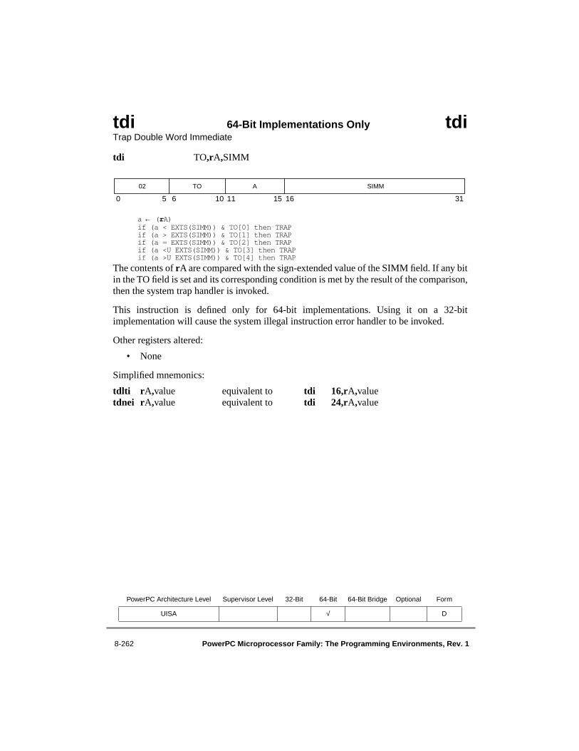
8-262 PowerPC Microprocessor Family: The Programming Environments, Rev. 1
tdi 64-Bit Implementations Only tdi Trap Double Word Immediate
tdi TO,rA,SIMM
a ← (rA)if (a < EXTS(SIMM)) & TO[0] then TRAPif (a > EXTS(SIMM)) & TO[1] then TRAPif (a = EXTS(SIMM)) & TO[2] then TRAPif (a <U EXTS(SIMM)) & TO[3] then TRAPif (a >U EXTS(SIMM)) & TO[4] then TRAP
The contents of rA are compared with the sign-extended value of the SIMM field. If any bitin the TO field is set and its corresponding condition is met by the result of the comparison,then the system trap handler is invoked.
This instruction is defined only for 64-bit implementations. Using it on a 32-bitimplementation will cause the system illegal instruction error handler to be invoked.
Other registers altered:
• None
Simplified mnemonics:
tdlti rA,value equivalent to tdi 16,rA,valuetdnei rA,value equivalent to tdi 24,rA,value
PowerPC Architecture Level Supervisor Level 32-Bit 64-Bit 64-Bit Bridge Optional Form
UISA √ D
0 5 6 10 11 15 16 31
02 TO A SIMM

Chapter 8. Instruction Set 8-263
tlbia tlbia Translation Lookaside Buffer Invalidate All
All TLB entries ← invalid
The entire translation lookaside buffer (TLB) is invalidated (that is, all entries areremoved).
The TLB is invalidated regardless of the settings of MSR[IR] and MSR[DR]. Theinvalidation is done without reference to the SLB, segment table, or segment registers.
This instruction does not cause the entries to be invalidated in other processors.
This is a supervisor-level instruction and optional in the PowerPC architecture.
Other registers altered:
• None
PowerPC Architecture Level Supervisor Level 32-Bit 64-Bit 64-Bit Bridge Optional Form
OEA √ √ X
0 0 0 0 0 370 0
0 5 6 10 11 15 16 20 21 30 31
Reserved
31 0 0 0 0 0 0 0 0 0 0

8-264 PowerPC Microprocessor Family: The Programming Environments, Rev. 1
tlbie tlbie Translation Lookaside Buffer Invalidate Entry
tlbie rB
[POWER mnemonic: tlbi]
VPS ← rB[36–51] Identify TLB entries corresponding to VPSEach such TLB entry ← invalid
EA is the contents of rB. If the translation lookaside buffer (TLB) contains an entrycorresponding to EA, that entry is made invalid (that is, removed from the TLB).
Multiprocessing implementations (for example, the 601, and 604) send a tlbie address-onlybroadcast over the address bus to tell other processors to invalidate the same TLB entry intheir TLBs.
The TLB search is done regardless of the settings of MSR[IR] and MSR[DR]. The searchis done based on a portion of the logical page number within a segment, without referenceto the SLB, segment table, or segment registers. All entries matching the search criteria areinvalidated.
Block address translation for EA, if any, is ignored. Refer to Section 7.5.3.4,“Synchronization of Memory Accesses and Referenced and Changed Bit Updates,” andSection 7.6.3, “Page Table Updates,” for other requirements associated with the use of thisinstruction.
This is a supervisor-level instruction and optional in the PowerPC architecture.
Other registers altered:
• None
PowerPC Architecture Level Supervisor Level 32-Bit 64-Bit 64-Bit Bridge Optional Form
OEA √ √ X
0 5 6 10 11 15 16 20 21 30 31
Reserved
31 0 0 0 0 0 0 0 0 0 0 B 30k6 0
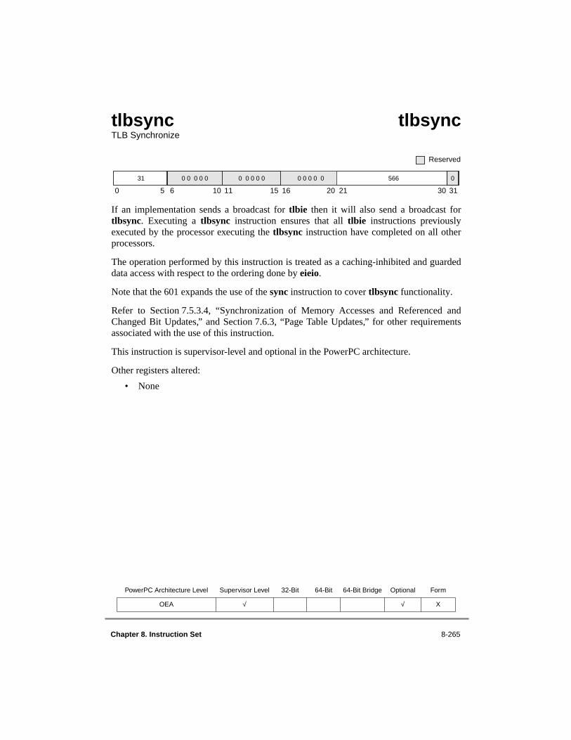
Chapter 8. Instruction Set 8-265
tlbsync tlbsyncTLB Synchronize
If an implementation sends a broadcast for tlbie then it will also send a broadcast fortlbsync. Executing a tlbsync instruction ensures that all tlbie instructions previouslyexecuted by the processor executing the tlbsync instruction have completed on all otherprocessors.
The operation performed by this instruction is treated as a caching-inhibited and guardeddata access with respect to the ordering done by eieio.
Note that the 601 expands the use of the sync instruction to cover tlbsync functionality.
Refer to Section 7.5.3.4, “Synchronization of Memory Accesses and Referenced andChanged Bit Updates,” and Section 7.6.3, “Page Table Updates,” for other requirementsassociated with the use of this instruction.
This instruction is supervisor-level and optional in the PowerPC architecture.
Other registers altered:
• None
PowerPC Architecture Level Supervisor Level 32-Bit 64-Bit 64-Bit Bridge Optional Form
OEA √ √ X
0 5 6 10 11 15 16 20 21 30 31
Reserved
31 0 0 0 0 0 0 0 0 0 0 0 0 0 0 0 566 0
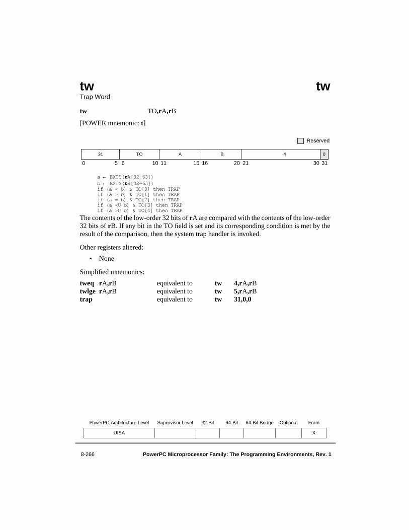
8-266 PowerPC Microprocessor Family: The Programming Environments, Rev. 1
tw tw Trap Word
tw TO,rA,rB
[POWER mnemonic: t]
a ← EXTS(rA[32–63])b ← EXTS(rB[32–63])if (a < b) & TO[0] then TRAPif (a > b) & TO[1] then TRAPif (a = b) & TO[2] then TRAPif (a <U b) & TO[3] then TRAPif (a >U b) & TO[4] then TRAP
The contents of the low-order 32 bits of rA are compared with the contents of the low-order32 bits of rB. If any bit in the TO field is set and its corresponding condition is met by theresult of the comparison, then the system trap handler is invoked.
Other registers altered:
• None
Simplified mnemonics:
tweq rA,rB equivalent to tw 4,rA,rBtwlge rA,rB equivalent to tw 5,rA,rBtrap equivalent to tw 31,0,0
PowerPC Architecture Level Supervisor Level 32-Bit 64-Bit 64-Bit Bridge Optional Form
UISA X
0 5 6 10 11 15 16 20 21 30 31
Reserved
31 TO A B 4 0

Chapter 8. Instruction Set 8-267
twi twi Trap Word Immediate
twi TO,rA,SIMM
[POWER mnemonic: ti]
a ← EXTS(rA[32–63])if (a < EXTS(SIMM)) & TO[0] then TRAPif (a > EXTS(SIMM)) & TO[1] then TRAPif (a = EXTS(SIMM)) & TO[2] then TRAPif (a <U EXTS(SIMM)) & TO[3] then TRAPif (a >U EXTS(SIMM)) & TO[4] then TRAP
The contents of the low-order 32 bits of rA are compared with the sign-extended value ofthe SIMM field. If any bit in the TO field is set and its corresponding condition is met bythe result of the comparison, then the system trap handler is invoked.
Other registers altered:
• None
Simplified mnemonics:
twgti rA,value equivalent to twi 8,rA,valuetwllei rA,value equivalent to twi 6,rA,value
PowerPC Architecture Level Supervisor Level 32-Bit 64-Bit 64-Bit Bridge Optional Form
UISA D
0 5 6 10 11 15 16 31
03 TO A SIMM
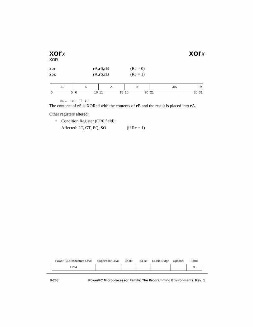
8-268 PowerPC Microprocessor Family: The Programming Environments, Rev. 1
xorx xorxXOR
xor rA,rS,rB (Rc = 0)xor. rA,rS,rB (Rc = 1)
rA ← (rS) ⊕ (rB)
The contents of rS is XORed with the contents of rB and the result is placed into rA.
Other registers altered:
• Condition Register (CR0 field):
Affected: LT, GT, EQ, SO (if Rc = 1)
PowerPC Architecture Level Supervisor Level 32-Bit 64-Bit 64-Bit Bridge Optional Form
UISA X
0 5 6 10 11 15 16 20 21 30 31
31 S A B 316 Rc

Chapter 8. Instruction Set 8-269
xori xori XOR Immediate
xori rA,rS,UIMM
[POWER mnemonic: xoril]
rA ← (rS) ⊕ ((48)0 || UIMM)
The contents of rS are XORed with 0x0000_0000_0000 || UIMM and the result is placedinto rA.
Other registers altered:
• None
PowerPC Architecture Level Supervisor Level 32-Bit 64-Bit 64-Bit Bridge Optional Form
UISA D
0 5 6 10 11 15 16 31
26 S A UIMM

8-270 PowerPC Microprocessor Family: The Programming Environments, Rev. 1
xoris xoris XOR Immediate Shifted
xoris rA,rS,UIMM
[POWER mnemonic: xoriu]
rA ← (rS) ⊕ ((32)0 || UIMM || (16)0)
The contents of rS are XORed with 0x0000_0000 || UIMM || 0x0000 and the result isplaced into rA.
Other registers altered:
• None
PowerPC Architecture Level Supervisor Level 32-Bit 64-Bit 64-Bit Bridge Optional Form
UISA D
0 5 6 10 11 15 16 31
27 S A UIMM

Appendix A. PowerPC Instruction Set Listings A-1
Appendix A PowerPC Instruction Set ListingsA0A0
This appendix lists the PowerPC architecture’s instruction set. Instructions are sorted bymnemonic, opcode, function, and form. Also included in this appendix is a quick referencetable that contains general information, such as the architecture level, privilege level, andform, and indicates if the instruction is 64-bit and/or optional.
Note that split fields, which represent the concatenation of sequences from left to right, areshown in lowercase. For more information refer to Chapter 8, “Instruction Set.”
A.1 Instructions Sorted by MnemonicTable A-1 lists the instructions implemented in the PowerPC architecture in alphabeticalorder by mnemonic.
Table A-1. Complete Instruction List Sorted by Mnemonic
Name 0 6 7 8 9 10 11 12 13 14 15 16 17 18 19 20 21 22 23 24 25 26 27 28 29 30 31
addx 31 D A B OE 266 Rc
addcx 31 D A B OE 10 Rc
addex 31 D A B OE 138 Rc
addi 14 D A SIMM
addic 12 D A SIMM
addic. 13 D A SIMM
addis 15 D A SIMM
addmex 31 D A 0 0 0 0 0 OE 234 Rc
addzex 31 D A 0 0 0 0 0 OE 202 Rc
andx 31 S A B 28 Rc
andcx 31 S A B 60 Rc
andi. 28 S A UIMM
Reserved bits
Key:

A-2 PowerPC Microprocessor Family: The Programming Environments, Rev 1
andis. 29 S A UIMM
bx 18 LI AA LK
bcx 16 BO BI BD AA LK
bcctrx 19 BO BI 0 0 0 0 0 528 LK
bclrx 19 BO BI 0 0 0 0 0 16 LK
cmp 31 crfD 0 L A B 0 0
cmpi 11 crfD 0 L A SIMM
cmpl 31 crfD 0 L A B 32 0
cmpli 10 crfD 0 L A UIMM
cntlzdx 1 31 S A 0 0 0 0 0 58 Rc
cntlzwx 31 S A 0 0 0 0 0 26 Rc
crand 19 crbD crbA crbB 257 0
crandc 19 crbD crbA crbB 129 0
creqv 19 crbD crbA crbB 289 0
crnand 19 crbD crbA crbB 225 0
crnor 19 crbD crbA crbB 33 0
cror 19 crbD crbA crbB 449 0
crorc 19 crbD crbA crbB 417 0
crxor 19 crbD crbA crbB 193 0
dcba 2 31 0 0 0 0 0 A B 758 0
dcbf 31 0 0 0 0 0 A B 86 0
dcbi 3 31 0 0 0 0 0 A B 470 0
dcbst 31 0 0 0 0 0 A B 54 0
dcbt 31 0 0 0 0 0 A B 278 0
dcbtst 31 0 0 0 0 0 A B 246 0
dcbz 31 0 0 0 0 0 A B 1014 0
divdx 1 31 D A B OE 489 Rc
divdux 1 31 D A B OE 457 Rc
divwx 31 D A B OE 491 Rc
divwux 31 D A B OE 459 Rc
eciwx 31 D A B 310 0
ecowx 31 S A B 438 0
eieio 31 0 0 0 0 0 0 0 0 0 0 0 0 0 0 0 854 0
Name 0 6 7 8 9 10 11 12 13 14 15 16 17 18 19 20 21 22 23 24 25 26 27 28 29 30 31

Appendix A. PowerPC Instruction Set Listings A-3
eqvx 31 S A B 284 Rc
extsbx 31 S A 0 0 0 0 0 954 Rc
extshx 31 S A 0 0 0 0 0 922 Rc
extswx 1 31 S A 0 0 0 0 0 986 Rc
fabsx 63 D 0 0 0 0 0 B 264 Rc
faddx 63 D A B 0 0 0 0 0 21 Rc
faddsx 59 D A B 0 0 0 0 0 21 Rc
fcfidx 1 63 D 0 0 0 0 0 B 846 Rc
fcmpo 63 crfD 0 0 A B 32 0
fcmpu 63 crfD 0 0 A B 0 0
fctidx 1 63 D 0 0 0 0 0 B 814 Rc
fctidzx 1 63 D 0 0 0 0 0 B 815 Rc
fctiwx 63 D 0 0 0 0 0 B 14 Rc
fctiwzx 63 D 0 0 0 0 0 B 15 Rc
fdivx 63 D A B 0 0 0 0 0 18 Rc
fdivsx 59 D A B 0 0 0 0 0 18 Rc
fmaddx 63 D A B C 29 Rc
fmaddsx 59 D A B C 29 Rc
fmrx 63 D 0 0 0 0 0 B 72 Rc
fmsubx 63 D A B C 28 Rc
fmsubsx 59 D A B C 28 Rc
fmulx 63 D A 0 0 0 0 0 C 25 Rc
fmulsx 59 D A 0 0 0 0 0 C 25 Rc
fnabsx 63 D 0 0 0 0 0 B 136 Rc
fnegx 63 D 0 0 0 0 0 B 40 Rc
fnmaddx 63 D A B C 31 Rc
fnmaddsx 59 D A B C 31 Rc
fnmsubx 63 D A B C 30 Rc
fnmsubsx 59 D A B C 30 Rc
fresx 2 59 D 0 0 0 0 0 B 0 0 0 0 0 24 Rc
frspx 63 D 0 0 0 0 0 B 12 Rc
frsqrtex 2 63 D 0 0 0 0 0 B 0 0 0 0 0 26 Rc
fselx 2 63 D A B C 23 Rc
Name 0 6 7 8 9 10 11 12 13 14 15 16 17 18 19 20 21 22 23 24 25 26 27 28 29 30 31
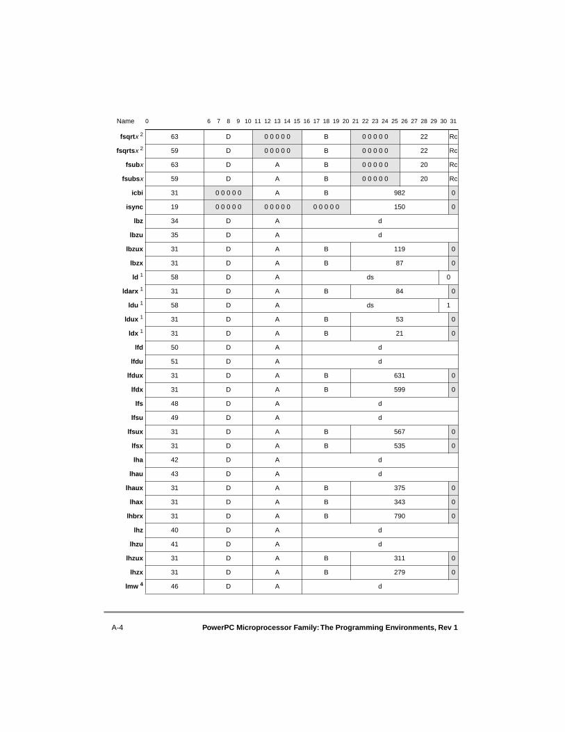
A-4 PowerPC Microprocessor Family: The Programming Environments, Rev 1
fsqrtx 2 63 D 0 0 0 0 0 B 0 0 0 0 0 22 Rc
fsqrtsx 2 59 D 0 0 0 0 0 B 0 0 0 0 0 22 Rc
fsubx 63 D A B 0 0 0 0 0 20 Rc
fsubsx 59 D A B 0 0 0 0 0 20 Rc
icbi 31 0 0 0 0 0 A B 982 0
isync 19 0 0 0 0 0 0 0 0 0 0 0 0 0 0 0 150 0
lbz 34 D A d
lbzu 35 D A d
lbzux 31 D A B 119 0
lbzx 31 D A B 87 0
ld 1 58 D A ds 0
ldarx 1 31 D A B 84 0
ldu 1 58 D A ds 1
ldux 1 31 D A B 53 0
ldx 1 31 D A B 21 0
lfd 50 D A d
lfdu 51 D A d
lfdux 31 D A B 631 0
lfdx 31 D A B 599 0
lfs 48 D A d
lfsu 49 D A d
lfsux 31 D A B 567 0
lfsx 31 D A B 535 0
lha 42 D A d
lhau 43 D A d
lhaux 31 D A B 375 0
lhax 31 D A B 343 0
lhbrx 31 D A B 790 0
lhz 40 D A d
lhzu 41 D A d
lhzux 31 D A B 311 0
lhzx 31 D A B 279 0
lmw 4 46 D A d
Name 0 6 7 8 9 10 11 12 13 14 15 16 17 18 19 20 21 22 23 24 25 26 27 28 29 30 31

Appendix A. PowerPC Instruction Set Listings A-5
lswi 4 31 D A NB 597 0
lswx 4 31 D A B 533 0
lwa 1 58 D A ds 2
lwarx 31 D A B 20 0
lwaux 1 31 D A B 373 0
lwax 1 31 D A B 341 0
lwbrx 31 D A B 534 0
lwz 32 D A d
lwzu 33 D A d
lwzux 31 D A B 55 0
lwzx 31 D A B 23 0
mcrf 19 crfD 0 0 crfS 0 0 0 0 0 0 0 0 0
mcrfs 63 crfD 0 0 crfS 0 0 0 0 0 0 0 64 0
mcrxr 31 crfD 0 0 0 0 0 0 0 0 0 0 0 0 512 0
mfcr 31 D 0 0 0 0 0 0 0 0 0 0 19 0
mffsx 63 D 0 0 0 0 0 0 0 0 0 0 583 Rc
mfmsr 3 31 D 0 0 0 0 0 0 0 0 0 0 83 0
mfspr 5 31 D spr 339 0
mfsr 3, 6 31 D 0 SR 0 0 0 0 0 595 0
mfsrin 3, 6 31 D 0 0 0 0 0 B 659 0
mftb 31 D tbr 371 0
mtcrf 31 S 0 CRM 0 144 0
mtfsb0x 63 crbD 0 0 0 0 0 0 0 0 0 0 70 Rc
mtfsb1x 63 crbD 0 0 0 0 0 0 0 0 0 0 38 Rc
mtfsfx 63 0 FM 0 B 711 Rc
mtfsfix 63 crfD 0 0 0 0 0 0 0 IMM 0 134 Rc
mtmsr 3, 6 31 S 0 0 0 0 0 0 0 0 0 0 146 0
mtmsrd 1, 3 31 S 0 0 0 0 0 0 0 0 0 0 178 0
mtspr 5 31 S spr 467 0
mtsr 3, 6 31 S 0 SR 0 0 0 0 0 210 0
mtsrd 3, 6 31 S 0 SR 0 0 0 0 0 82 0
mtsrdin 3,6 31 S 0 0 0 0 0 B 114 0
mtsrin 3, 6 31 S 0 0 0 0 0 B 242 0
Name 0 6 7 8 9 10 11 12 13 14 15 16 17 18 19 20 21 22 23 24 25 26 27 28 29 30 31

A-6 PowerPC Microprocessor Family: The Programming Environments, Rev 1
mulhdx 1 31 D A B 0 73 Rc
mulhdux1 31 D A B 0 9 Rc
mulhwx 31 D A B 0 75 Rc
mulhwux 31 D A B 0 11 Rc
mulldx 1 31 D A B OE 233 Rc
mulli 7 D A SIMM
mullwx 31 D A B OE 235 Rc
nandx 31 S A B 476 Rc
negx 31 D A 0 0 0 0 0 OE 104 Rc
norx 31 S A B 124 Rc
orx 31 S A B 444 Rc
orcx 31 S A B 412 Rc
ori 24 S A UIMM
oris 25 S A UIMM
rfi 3, 6 19 0 0 0 0 0 0 0 0 0 0 0 0 0 0 0 50 0
rfid 1, 3 19 0 0 0 0 0 0 0 0 0 0 0 0 0 0 0 18 0
rldclx 1 30 S A B mb 8 Rc
rldcrx 1 30 S A B me 9 Rc
rldicx 1 30 S A sh mb 2 sh Rc
rldiclx 1 30 S A sh mb 0 sh Rc
rldicrx 1 30 S A sh me 1 sh Rc
rldimix 1 30 S A sh mb 3 sh Rc
rlwimix 20 S A SH MB ME Rc
rlwinmx 21 S A SH MB ME Rc
rlwnmx 23 S A B MB ME Rc
sc 17 0 0 0 0 0 0 0 0 0 0 0 0 0 0 0 0 0 0 0 0 0 0 0 0 1 0
slbia 1,2,3 31 0 0 0 0 0 0 0 0 0 0 0 0 0 0 0 498 0
slbie 1,2,3 31 0 0 0 0 0 0 0 0 0 0 B 434 0
sldx 1 31 S A B 27 Rc
slwx 31 S A B 24 Rc
sradx 1 31 S A B 794 Rc
sradix 1 31 S A sh 413 sh Rc
srawx 31 S A B 792 Rc
Name 0 6 7 8 9 10 11 12 13 14 15 16 17 18 19 20 21 22 23 24 25 26 27 28 29 30 31

Appendix A. PowerPC Instruction Set Listings A-7
srawix 31 S A SH 824 Rc
srdx 1 31 S A B 539 Rc
srwx 31 S A B 536 Rc
stb 38 S A d
stbu 39 S A d
stbux 31 S A B 247 0
stbx 31 S A B 215 0
std 1 62 S A ds 0
stdcx. 1 31 S A B 214 1
stdu 1 62 S A ds 1
stdux 1 31 S A B 181 0
stdx 1 31 S A B 149 0
stfd 54 S A d
stfdu 55 S A d
stfdux 31 S A B 759 0
stfdx 31 S A B 727 0
stfiwx 2 31 S A B 983 0
stfs 52 S A d
stfsu 53 S A d
stfsux 31 S A B 695 0
stfsx 31 S A B 663 0
sth 44 S A d
sthbrx 31 S A B 918 0
sthu 45 S A d
sthux 31 S A B 439 0
sthx 31 S A B 407 0
stmw 4 47 S A d
stswi 4 31 S A NB 725 0
stswx 4 31 S A B 661 0
stw 36 S A d
stwbrx 31 S A B 662 0
stwcx. 31 S A B 150 1
stwu 37 S A d
Name 0 6 7 8 9 10 11 12 13 14 15 16 17 18 19 20 21 22 23 24 25 26 27 28 29 30 31
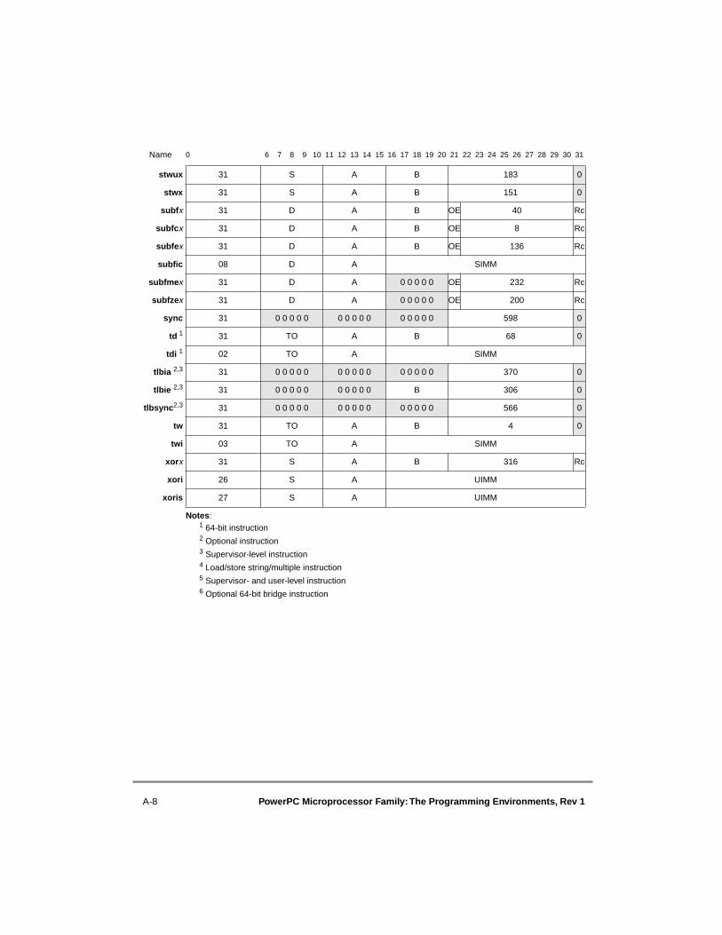
A-8 PowerPC Microprocessor Family: The Programming Environments, Rev 1
1 64-bit instruction2 Optional instruction 3 Supervisor-level instruction4 Load/store string/multiple instruction5 Supervisor- and user-level instruction6 Optional 64-bit bridge instruction
stwux 31 S A B 183 0
stwx 31 S A B 151 0
subfx 31 D A B OE 40 Rc
subfcx 31 D A B OE 8 Rc
subfex 31 D A B OE 136 Rc
subfic 08 D A SIMM
subfmex 31 D A 0 0 0 0 0 OE 232 Rc
subfzex 31 D A 0 0 0 0 0 OE 200 Rc
sync 31 0 0 0 0 0 0 0 0 0 0 0 0 0 0 0 598 0
td 1 31 TO A B 68 0
tdi 1 02 TO A SIMM
tlbia 2,3 31 0 0 0 0 0 0 0 0 0 0 0 0 0 0 0 370 0
tlbie 2,3 31 0 0 0 0 0 0 0 0 0 0 B 306 0
tlbsync2,3 31 0 0 0 0 0 0 0 0 0 0 0 0 0 0 0 566 0
tw 31 TO A B 4 0
twi 03 TO A SIMM
xorx 31 S A B 316 Rc
xori 26 S A UIMM
xoris 27 S A UIMM
Notes:
Name 0 6 7 8 9 10 11 12 13 14 15 16 17 18 19 20 21 22 23 24 25 26 27 28 29 30 31
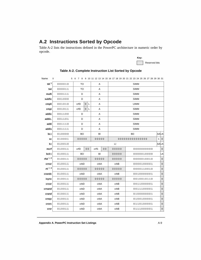
Appendix A. PowerPC Instruction Set Listings A-9
A.2 Instructions Sorted by OpcodeTable A-2 lists the instructions defined in the PowerPC architecture in numeric order byopcode.
Table A-2. Complete Instruction List Sorted by Opcode
Name 0 5 6 7 8 9 10 11 12 13 14 15 16 17 18 19 20 21 22 23 24 25 26 27 28 29 30 31
tdi 1 0 0 0 0 1 0 TO A SIMM
twi 0 0 0 0 1 1 TO A SIMM
mulli 0 0 0 1 1 1 D A SIMM
subfic 0 0 1 0 0 0 D A SIMM
cmpli 0 0 1 0 1 0 crfD 0 L A UIMM
cmpi 0 0 1 0 1 1 crfD 0 L A SIMM
addic 0 0 1 1 0 0 D A SIMM
addic. 0 0 1 1 0 1 D A SIMM
addi 0 0 1 1 1 0 D A SIMM
addis 0 0 1 1 1 1 D A SIMM
bcx 0 1 0 0 0 0 BO BI BD AA LK
sc 0 1 0 0 0 1 0 0 0 0 0 0 0 0 0 0 0 0 0 0 0 0 0 0 0 0 0 0 0 0 0 1 0
bx 0 1 0 0 1 0 LI AA LK
mcrf 0 1 0 0 1 1 crfD 0 0 crfS 0 0 0 0 0 0 0 0 0 0 0 0 0 0 0 0 0 0
bclrx 0 1 0 0 1 1 BO BI 0 0 0 0 0 0 0 0 0 0 1 0 0 0 0 LK
rfid 1, 2 0 1 0 0 1 1 0 0 0 0 0 0 0 0 0 0 0 0 0 0 0 0 0 0 0 0 1 0 0 1 0 0
crnor 0 1 0 0 1 1 crbD crbA crbB 0 0 0 0 1 0 0 0 0 1 0
rfi 2, 3 0 1 0 0 1 1 0 0 0 0 0 0 0 0 0 0 0 0 0 0 0 0 0 0 0 1 1 0 0 1 0 0
crandc 0 1 0 0 1 1 crbD crbA crbB 0 0 1 0 0 0 0 0 0 1 0
isync 0 1 0 0 1 1 0 0 0 0 0 0 0 0 0 0 0 0 0 0 0 0 0 1 0 0 1 0 1 1 0 0
crxor 0 1 0 0 1 1 crbD crbA crbB 0 0 1 1 0 0 0 0 0 1 0
crnand 0 1 0 0 1 1 crbD crbA crbB 0 0 1 1 1 0 0 0 0 1 0
crand 0 1 0 0 1 1 crbD crbA crbB 0 1 0 0 0 0 0 0 0 1 0
creqv 0 1 0 0 1 1 crbD crbA crbB 0 1 0 0 1 0 0 0 0 1 0
crorc 0 1 0 0 1 1 crbD crbA crbB 0 1 1 0 1 0 0 0 0 1 0
cror 0 1 0 0 1 1 crbD crbA crbB 0 1 1 1 0 0 0 0 0 1 0
Reserved bits
Key:

A-10 PowerPC Microprocessor Family: The Programming Environments, Rev 1
bcctrx 0 1 0 0 1 1 BO BI 0 0 0 0 0 1 0 0 0 0 1 0 0 0 0 LK
rlwimix 0 1 0 1 0 0 S A SH MB ME Rc
rlwinmx 0 1 0 1 0 1 S A SH MB ME Rc
rlwnmx 0 1 0 1 1 1 S A B MB ME Rc
ori 0 1 1 0 0 0 S A UIMM
oris 0 1 1 0 0 1 S A UIMM
xori 0 1 1 0 1 0 S A UIMM
xoris 0 1 1 0 1 1 S A UIMM
andi. 0 1 1 1 0 0 S A UIMM
andis. 0 1 1 1 0 1 S A UIMM
rldiclx 1 0 1 1 1 1 0 S A sh mb 0 0 0 sh Rc
rldicrx 1 0 1 1 1 1 0 S A sh me 0 0 1 sh Rc
rldicx 1 0 1 1 1 1 0 S A sh mb 0 1 0 sh Rc
rldimix 1 0 1 1 1 1 0 S A sh mb 0 1 1 sh Rc
rldclx 1 0 1 1 1 1 0 S A B mb 0 1 0 0 0 Rc
rldcrx 1 0 1 1 1 1 0 S A B me 0 1 0 0 1 Rc
cmp 0 1 1 1 1 1 crfD 0 L A B 0 0 0 0 0 0 0 0 0 0 0
tw 0 1 1 1 1 1 TO A B 0 0 0 0 0 0 0 1 0 0 0
subfcx 0 1 1 1 1 1 D A B OE 0 0 0 0 0 0 1 0 0 0 Rc
mulhdux 1 0 1 1 1 1 1 D A B 0 0 0 0 0 0 0 1 0 0 1 Rc
addcx 0 1 1 1 1 1 D A B OE 0 0 0 0 0 0 1 0 1 0 Rc
mulhwux 0 1 1 1 1 1 D A B 0 0 0 0 0 0 0 1 0 1 1 Rc
mfcr 0 1 1 1 1 1 D 0 0 0 0 0 0 0 0 0 0 0 0 0 0 0 1 0 0 1 1 0
lwarx 0 1 1 1 1 1 D A B 0 0 0 0 0 1 0 1 0 0 0
ldx 1 0 1 1 1 1 1 D A B 0 0 0 0 0 1 0 1 0 1 0
lwzx 0 1 1 1 1 1 D A B 0 0 0 0 0 1 0 1 1 1 0
slwx 0 1 1 1 1 1 S A B 0 0 0 0 0 1 1 0 0 0 Rc
cntlzwx 0 1 1 1 1 1 S A 0 0 0 0 0 0 0 0 0 0 1 1 0 1 0 Rc
sldx 1 0 1 1 1 1 1 S A B 0 0 0 0 0 1 1 0 1 1 Rc
andx 0 1 1 1 1 1 S A B 0 0 0 0 0 1 1 1 0 0 Rc
cmpl 0 1 1 1 1 1 crfD 0 L A B 0 0 0 0 1 0 0 0 0 0 0
subfx 0 1 1 1 1 1 D A B OE 0 0 0 0 1 0 1 0 0 0 Rc
ldux 1 0 1 1 1 1 1 D A B 0 0 0 0 1 1 0 1 0 1 0
Name 0 5 6 7 8 9 10 11 12 13 14 15 16 17 18 19 20 21 22 23 24 25 26 27 28 29 30 31

Appendix A. PowerPC Instruction Set Listings A-11
dcbst 0 1 1 1 1 1 0 0 0 0 0 A B 0 0 0 0 1 1 0 1 1 0 0
lwzux 0 1 1 1 1 1 D A B 0 0 0 0 1 1 0 1 1 1 0
cntlzdx 1 0 1 1 1 1 1 S A 0 0 0 0 0 0 0 0 0 1 1 1 0 1 0 Rc
andcx 0 1 1 1 1 1 S A B 0 0 0 0 1 1 1 1 0 0 Rc
td 1 0 1 1 1 1 1 TO A B 0 0 0 1 0 0 0 1 0 0 0
mulhdx 1 0 1 1 1 1 1 D A B 0 0 0 0 1 0 0 1 0 0 1 Rc
mulhwx 0 1 1 1 1 1 D A B 0 0 0 0 1 0 0 1 0 1 1 Rc
mtsrd 2, 3 0 1 1 1 1 1 S 0 SR 0 0 0 0 0 0 0 0 1 0 1 0 0 1 0 0
mfmsr2 0 1 1 1 1 1 D 0 0 0 0 0 0 0 0 0 0 0 0 0 1 0 1 0 0 1 1 0
ldarx 1 0 1 1 1 1 1 D A B 0 0 0 1 0 1 0 1 0 0 0
dcbf 0 1 1 1 1 1 0 0 0 0 0 A B 0 0 0 1 0 1 0 1 1 0 0
lbzx 0 1 1 1 1 1 D A B 0 0 0 1 0 1 0 1 1 1 0
negx 0 1 1 1 1 1 D A 0 0 0 0 0 OE 0 0 0 1 1 0 1 0 0 0 Rc
mtsrdin 2, 3 0 1 1 1 1 1 S 0 0 0 0 0 B 0 0 0 1 1 1 0 0 1 0 0
lbzux 0 1 1 1 1 1 D A B 0 0 0 1 1 1 0 1 1 1 0
norx 0 1 1 1 1 1 S A B 0 0 0 1 1 1 1 1 0 0 Rc
subfex 0 1 1 1 1 1 D A B OE 0 0 1 0 0 0 1 0 0 0 Rc
addex 0 1 1 1 1 1 D A B OE 0 0 1 0 0 0 1 0 1 0 Rc
mtcrf 0 1 1 1 1 1 S 0 CRM 0 0 0 1 0 0 1 0 0 0 0 0
mtmsr 2, 3 0 1 1 1 1 1 S 0 0 0 0 0 0 0 0 0 0 0 0 1 0 0 1 0 0 1 0 0
stdx 1 0 1 1 1 1 1 S A B 0 0 1 0 0 1 0 1 0 1 0
stwcx. 0 1 1 1 1 1 S A B 0 0 1 0 0 1 0 1 1 0 1
stwx 0 1 1 1 1 1 S A B 0 0 1 0 0 1 0 1 1 1 0
mtmsrd 1, 2 0 1 1 1 1 1 S 0 0 0 0 0 0 0 0 0 0 0 0 1 0 1 1 0 0 1 0 0
stdux 1 0 1 1 1 1 1 S A B 0 0 1 0 1 1 0 1 0 1 0
stwux 0 1 1 1 1 1 S A B 0 0 1 0 1 1 0 1 1 1 0
subfzex 0 1 1 1 1 1 D A 0 0 0 0 0 OE 0 0 1 1 0 0 1 0 0 0 Rc
addzex 0 1 1 1 1 1 D A 0 0 0 0 0 OE 0 0 1 1 0 0 1 0 1 0 Rc
mtsr 2,3 0 1 1 1 1 1 S 0 SR 0 0 0 0 0 0 0 1 1 0 1 0 0 1 0 0
stdcx. 1 0 1 1 1 1 1 S A B 0 0 1 1 0 1 0 1 1 0 1
stbx 0 1 1 1 1 1 S A B 0 0 1 1 0 1 0 1 1 1 0
subfmex 0 1 1 1 1 1 D A 0 0 0 0 0 OE 0 0 1 1 1 0 1 0 0 0 Rc
mulld1 0 1 1 1 1 1 D A B OE 0 0 1 1 1 0 1 0 0 1 Rc
Name 0 5 6 7 8 9 10 11 12 13 14 15 16 17 18 19 20 21 22 23 24 25 26 27 28 29 30 31
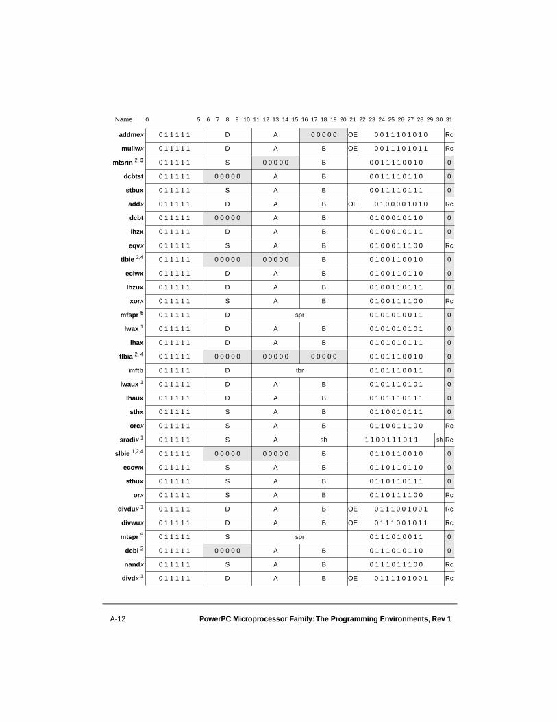
A-12 PowerPC Microprocessor Family: The Programming Environments, Rev 1
addmex 0 1 1 1 1 1 D A 0 0 0 0 0 OE 0 0 1 1 1 0 1 0 1 0 Rc
mullwx 0 1 1 1 1 1 D A B OE 0 0 1 1 1 0 1 0 1 1 Rc
mtsrin 2, 3 0 1 1 1 1 1 S 0 0 0 0 0 B 0 0 1 1 1 1 0 0 1 0 0
dcbtst 0 1 1 1 1 1 0 0 0 0 0 A B 0 0 1 1 1 1 0 1 1 0 0
stbux 0 1 1 1 1 1 S A B 0 0 1 1 1 1 0 1 1 1 0
addx 0 1 1 1 1 1 D A B OE 0 1 0 0 0 0 1 0 1 0 Rc
dcbt 0 1 1 1 1 1 0 0 0 0 0 A B 0 1 0 0 0 1 0 1 1 0 0
lhzx 0 1 1 1 1 1 D A B 0 1 0 0 0 1 0 1 1 1 0
eqvx 0 1 1 1 1 1 S A B 0 1 0 0 0 1 1 1 0 0 Rc
tlbie 2,4 0 1 1 1 1 1 0 0 0 0 0 0 0 0 0 0 B 0 1 0 0 1 1 0 0 1 0 0
eciwx 0 1 1 1 1 1 D A B 0 1 0 0 1 1 0 1 1 0 0
lhzux 0 1 1 1 1 1 D A B 0 1 0 0 1 1 0 1 1 1 0
xorx 0 1 1 1 1 1 S A B 0 1 0 0 1 1 1 1 0 0 Rc
mfspr 5 0 1 1 1 1 1 D spr 0 1 0 1 0 1 0 0 1 1 0
lwax 1 0 1 1 1 1 1 D A B 0 1 0 1 0 1 0 1 0 1 0
lhax 0 1 1 1 1 1 D A B 0 1 0 1 0 1 0 1 1 1 0
tlbia 2, 4 0 1 1 1 1 1 0 0 0 0 0 0 0 0 0 0 0 0 0 0 0 0 1 0 1 1 1 0 0 1 0 0
mftb 0 1 1 1 1 1 D tbr 0 1 0 1 1 1 0 0 1 1 0
lwaux 1 0 1 1 1 1 1 D A B 0 1 0 1 1 1 0 1 0 1 0
lhaux 0 1 1 1 1 1 D A B 0 1 0 1 1 1 0 1 1 1 0
sthx 0 1 1 1 1 1 S A B 0 1 1 0 0 1 0 1 1 1 0
orcx 0 1 1 1 1 1 S A B 0 1 1 0 0 1 1 1 0 0 Rc
sradix 1 0 1 1 1 1 1 S A sh 1 1 0 0 1 1 1 0 1 1 sh Rc
slbie 1,2,4 0 1 1 1 1 1 0 0 0 0 0 0 0 0 0 0 B 0 1 1 0 1 1 0 0 1 0 0
ecowx 0 1 1 1 1 1 S A B 0 1 1 0 1 1 0 1 1 0 0
sthux 0 1 1 1 1 1 S A B 0 1 1 0 1 1 0 1 1 1 0
orx 0 1 1 1 1 1 S A B 0 1 1 0 1 1 1 1 0 0 Rc
divdux 1 0 1 1 1 1 1 D A B OE 0 1 1 1 0 0 1 0 0 1 Rc
divwux 0 1 1 1 1 1 D A B OE 0 1 1 1 0 0 1 0 1 1 Rc
mtspr 5 0 1 1 1 1 1 S spr 0 1 1 1 0 1 0 0 1 1 0
dcbi 2 0 1 1 1 1 1 0 0 0 0 0 A B 0 1 1 1 0 1 0 1 1 0 0
nandx 0 1 1 1 1 1 S A B 0 1 1 1 0 1 1 1 0 0 Rc
divdx 1 0 1 1 1 1 1 D A B OE 0 1 1 1 1 0 1 0 0 1 Rc
Name 0 5 6 7 8 9 10 11 12 13 14 15 16 17 18 19 20 21 22 23 24 25 26 27 28 29 30 31
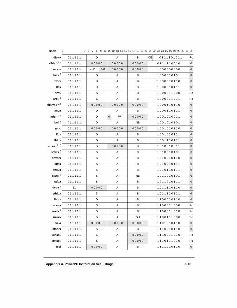
Appendix A. PowerPC Instruction Set Listings A-13
divwx 0 1 1 1 1 1 D A B OE 0 1 1 1 1 0 1 0 1 1 Rc
slbia 1,2,4 0 1 1 1 1 1 0 0 0 0 0 0 0 0 0 0 0 0 0 0 0 0 1 1 1 1 1 0 0 1 0 0
mcrxr 0 1 1 1 1 1 crfD 0 0 0 0 0 0 0 0 0 0 0 0 1 0 0 0 0 0 0 0 0 0 0
lswx 6 0 1 1 1 1 1 D A B 1 0 0 0 0 1 0 1 0 1 0
lwbrx 0 1 1 1 1 1 D A B 1 0 0 0 0 1 0 1 1 0 0
lfsx 0 1 1 1 1 1 D A B 1 0 0 0 0 1 0 1 1 1 0
srwx 0 1 1 1 1 1 S A B 1 0 0 0 0 1 1 0 0 0 Rc
srdx 1 0 1 1 1 1 1 S A B 1 0 0 0 0 1 1 0 1 1 Rc
tlbsync 2,4 0 1 1 1 1 1 0 0 0 0 0 0 0 0 0 0 0 0 0 0 0 1 0 0 0 1 1 0 1 1 0 0
lfsux 0 1 1 1 1 1 D A B 1 0 0 0 1 1 0 1 1 1 0
mfsr 2, 3 0 1 1 1 1 1 D 0 SR 0 0 0 0 0 1 0 0 1 0 1 0 0 1 1 0
lswi 6 0 1 1 1 1 1 D A NB 1 0 0 1 0 1 0 1 0 1 0
sync 0 1 1 1 1 1 0 0 0 0 0 0 0 0 0 0 0 0 0 0 0 1 0 0 1 0 1 0 1 1 0 0
lfdx 0 1 1 1 1 1 D A B 1 0 0 1 0 1 0 1 1 1 0
lfdux 0 1 1 1 1 1 D A B 1 0 0 1 1 1 0 1 1 1 0
mfsrin 2, 3 0 1 1 1 1 1 D 0 0 0 0 0 B 1 0 1 0 0 1 0 0 1 1 0
stswx 6 0 1 1 1 1 1 S A B 1 0 1 0 0 1 0 1 0 1 0
stwbrx 0 1 1 1 1 1 S A B 1 0 1 0 0 1 0 1 1 0 0
stfsx 0 1 1 1 1 1 S A B 1 0 1 0 0 1 0 1 1 1 0
stfsux 0 1 1 1 1 1 S A B 1 0 1 0 1 1 0 1 1 1 0
stswi 6 0 1 1 1 1 1 S A NB 1 0 1 1 0 1 0 1 0 1 0
stfdx 0 1 1 1 1 1 S A B 1 0 1 1 0 1 0 1 1 1 0
dcba 4 31 0 0 0 0 0 A B 1 0 1 1 1 1 0 1 1 0 0
stfdux 0 1 1 1 1 1 S A B 1 0 1 1 1 1 0 1 1 1 0
lhbrx 0 1 1 1 1 1 D A B 1 1 0 0 0 1 0 1 1 0 0
srawx 0 1 1 1 1 1 S A B 1 1 0 0 0 1 1 0 0 0 Rc
sradx 1 0 1 1 1 1 1 S A B 1 1 0 0 0 1 1 0 1 0 Rc
srawix 0 1 1 1 1 1 S A SH 1 1 0 0 1 1 1 0 0 0 Rc
eieio 0 1 1 1 1 1 0 0 0 0 0 0 0 0 0 0 0 0 0 0 0 1 1 0 1 0 1 0 1 1 0 0
sthbrx 0 1 1 1 1 1 S A B 1 1 1 0 0 1 0 1 1 0 0
extshx 0 1 1 1 1 1 S A 0 0 0 0 0 1 1 1 0 0 1 1 0 1 0 Rc
extsbx 0 1 1 1 1 1 S A 0 0 0 0 0 1 1 1 0 1 1 1 0 1 0 Rc
icbi 0 1 1 1 1 1 0 0 0 0 0 A B 1 1 1 1 0 1 0 1 1 0 0
Name 0 5 6 7 8 9 10 11 12 13 14 15 16 17 18 19 20 21 22 23 24 25 26 27 28 29 30 31

A-14 PowerPC Microprocessor Family: The Programming Environments, Rev 1
stfiwx 4 0 1 1 1 1 1 S A B 1 1 1 1 0 1 0 1 1 1 0
extsw 1 0 1 1 1 1 1 S A 0 0 0 0 0 1 1 1 1 0 1 1 0 1 0 Rc
dcbz 0 1 1 1 1 1 0 0 0 0 0 A B 1 1 1 1 1 1 0 1 1 0 0
lwz 1 0 0 0 0 0 D A d
lwzu 1 0 0 0 0 1 D A d
lbz 1 0 0 0 1 0 D A d
lbzu 1 0 0 0 1 1 D A d
stw 1 0 0 1 0 0 S A d
stwu 1 0 0 1 0 1 S A d
stb 1 0 0 1 1 0 S A d
stbu 1 0 0 1 1 1 S A d
lhz 1 0 1 0 0 0 D A d
lhzu 1 0 1 0 0 1 D A d
lha 1 0 1 0 1 0 D A d
lhau 1 0 1 0 1 1 D A d
sth 1 0 1 1 0 0 S A d
sthu 1 0 1 1 0 1 S A d
lmw 6 1 0 1 1 1 0 D A d
stmw 6 1 0 1 1 1 1 S A d
lfs 1 1 0 0 0 0 D A d
lfsu 1 1 0 0 0 1 D A d
lfd 1 1 0 0 1 0 D A d
lfdu 1 1 0 0 1 1 D A d
stfs 1 1 0 1 0 0 S A d
stfsu 1 1 0 1 0 1 S A d
stfd 1 1 0 1 1 0 S A d
stfdu 1 1 0 1 1 1 S A d
ld 1 1 1 1 0 1 0 D A ds 0 0
ldu 1 1 1 1 0 1 0 D A ds 0 1
lwa 1 1 1 1 0 1 0 D A ds 1 0
fdivsx 1 1 1 0 1 1 D A B 0 0 0 0 0 1 0 0 1 0 Rc
fsubsx 1 1 1 0 1 1 D A B 0 0 0 0 0 1 0 1 0 0 Rc
faddsx 1 1 1 0 1 1 D A B 0 0 0 0 0 1 0 1 0 1 Rc
Name 0 5 6 7 8 9 10 11 12 13 14 15 16 17 18 19 20 21 22 23 24 25 26 27 28 29 30 31

Appendix A. PowerPC Instruction Set Listings A-15
fsqrtsx 4 1 1 1 0 1 1 D 0 0 0 0 0 B 0 0 0 0 0 1 0 1 1 0 Rc
fresx 4 1 1 1 0 1 1 D 0 0 0 0 0 B 0 0 0 0 0 1 1 0 0 0 Rc
fmulsx 1 1 1 0 1 1 D A 0 0 0 0 0 C 1 1 0 0 1 Rc
fmsubsx 1 1 1 0 1 1 D A B C 1 1 1 0 0 Rc
fmaddsx 1 1 1 0 1 1 D A B C 1 1 1 0 1 Rc
fnmsubsx 1 1 1 0 1 1 D A B C 1 1 1 1 0 Rc
fnmaddsx 1 1 1 0 1 1 D A B C 1 1 1 1 1 Rc
std 1 1 1 1 1 1 0 S A ds 0 0
stdu 1 1 1 1 1 1 0 S A ds 0 1
fcmpu 1 1 1 1 1 1 crfD 0 0 A B 0 0 0 0 0 0 0 0 0 0 0
frspx 1 1 1 1 1 1 D 0 0 0 0 0 B 0 0 0 0 0 0 1 1 0 0 Rc
fctiwx 1 1 1 1 1 1 D 0 0 0 0 0 B 0 0 0 0 0 0 1 1 1 0
fctiwzx 1 1 1 1 1 1 D 0 0 0 0 0 B 0 0 0 0 0 0 1 1 1 1 Rc
fdivx 1 1 1 1 1 1 D A B 0 0 0 0 0 1 0 0 1 0 Rc
fsubx 1 1 1 1 1 1 D A B 0 0 0 0 0 1 0 1 0 0 Rc
faddx 1 1 1 1 1 1 D A B 0 0 0 0 0 1 0 1 0 1 Rc
fsqrtx 4 1 1 1 1 1 1 D 0 0 0 0 0 B 0 0 0 0 0 1 0 1 1 0 Rc
fselx 4 1 1 1 1 1 1 D A B C 1 0 1 1 1 Rc
fmulx 1 1 1 1 1 1 D A 0 0 0 0 0 C 1 1 0 0 1 Rc
frsqrtex 1 1 1 1 1 1 1 D 0 0 0 0 0 B 0 0 0 0 0 1 1 0 1 0 Rc
fmsubx 1 1 1 1 1 1 D A B C 1 1 1 0 0 Rc
fmaddx 1 1 1 1 1 1 D A B C 1 1 1 0 1 Rc
fnmsubx 1 1 1 1 1 1 D A B C 1 1 1 1 0 Rc
fnmaddx 1 1 1 1 1 1 D A B C 1 1 1 1 1 Rc
fcmpo 1 1 1 1 1 1 crfD 0 0 A B 0 0 0 0 1 0 0 0 0 0 0
mtfsb1x 1 1 1 1 1 1 crbD 0 0 0 0 0 0 0 0 0 0 0 0 0 0 1 0 0 1 1 0 Rc
fnegx 1 1 1 1 1 1 D 0 0 0 0 0 B 0 0 0 0 1 0 1 0 0 0 Rc
mcrfs 1 1 1 1 1 1 crfD 0 0 crfS 0 0 0 0 0 0 0 0 0 0 1 0 0 0 0 0 0 0
mtfsb0x 1 1 1 1 1 1 crbD 0 0 0 0 0 0 0 0 0 0 0 0 0 1 0 0 0 1 1 0 Rc
fmrx 1 1 1 1 1 1 D 0 0 0 0 0 B 0 0 0 1 0 0 1 0 0 0 Rc
mtfsfix 1 1 1 1 1 1 crfD 0 0 0 0 0 0 0 IMM 0 0 0 1 0 0 0 0 1 1 0 Rc
fnabsx 1 1 1 1 1 1 D 0 0 0 0 0 B 0 0 1 0 0 0 1 0 0 0 Rc
fabsx 1 1 1 1 1 1 D 0 0 0 0 0 B 0 1 0 0 0 0 1 0 0 0 Rc
Name 0 5 6 7 8 9 10 11 12 13 14 15 16 17 18 19 20 21 22 23 24 25 26 27 28 29 30 31

A-16 PowerPC Microprocessor Family: The Programming Environments, Rev 1
1 64-bit instruction2 Supervisor-level instruction3 Optional 64-bit bridge instruction4 Optional instruction5 Supervisor- and user-level instruction6 Load/store string/multiple instruction
mffsx 1 1 1 1 1 1 D 0 0 0 0 0 0 0 0 0 0 1 0 0 1 0 0 0 1 1 1 Rc
mtfsfx 1 1 1 1 1 1 0 FM 0 B 1 0 1 1 0 0 0 1 1 1 Rc
fctidx 1 1 1 1 1 1 1 D 0 0 0 0 0 B 1 1 0 0 1 0 1 1 1 0 Rc
fctidzx 1 1 1 1 1 1 1 D 0 0 0 0 0 B 1 1 0 0 1 0 1 1 1 1 Rc
fcfidx 1 1 1 1 1 1 1 D 0 0 0 0 0 B 1 1 0 1 0 0 1 1 1 0 Rc
Notes:
Name 0 5 6 7 8 9 10 11 12 13 14 15 16 17 18 19 20 21 22 23 24 25 26 27 28 29 30 31

Appendix A. PowerPC Instruction Set Listings A-17
A.3 Instructions Grouped by Functional CategoriesTable A-3 through Table A-30 list the PowerPC instructions grouped by function.
Table A-3. Integer Arithmetic Instructions
1 64-bit instruction
Name 0 5 6 7 8 9 10 11 12 13 14 15 16 17 18 19 20 21 22 23 24 25 26 27 28 29 30 31
addx 31 D A B OE 266 Rc
addcx 31 D A B OE 10 Rc
addex 31 D A B OE 138 Rc
addi 14 D A SIMM
addic 12 D A SIMM
addic. 13 D A SIMM
addis 15 D A SIMM
addmex 31 D A 0 0 0 0 0 OE 234 Rc
addzex 31 D A 0 0 0 0 0 OE 202 Rc
divdx 1 31 D A B OE 489 Rc
divdux 1 31 D A B OE 457 Rc
divwx 31 D A B OE 491 Rc
divwux 31 D A B OE 459 Rc
mulhdx 1 31 D A B 0 73 Rc
mulhdux1 31 D A B 0 9 Rc
mulhwx 31 D A B 0 75 Rc
mulhwux 31 D A B 0 11 Rc
mulld 1 31 D A B OE 233 Rc
mulli 07 D A SIMM
mullwx 31 D A B OE 235 Rc
negx 31 D A 0 0 0 0 0 OE 104 Rc
subfx 31 D A B OE 40 Rc
subfcx 31 D A B OE 8 Rc
subficx 08 D A SIMM
subfex 31 D A B OE 136 Rc
subfmex 31 D A 0 0 0 0 0 OE 232 Rc
subfzex 31 D A 0 0 0 0 0 OE 200 Rc
Note:
Reserved bitsKey:

A-18 PowerPC Microprocessor Family: The Programming Environments, Rev 1
Table A-4. Integer Compare Instructions
Table A-5. Integer Logical Instructions
1 64-bit instruction
Name 0 5 6 7 8 9 10 11 12 13 14 15 16 17 18 19 20 21 22 23 24 25 26 27 28 29 30 31
cmp 31 crfD 0 L A B 0 0 0 0 0 0 0 0 0 0 0
cmpi 11 crfD 0 L A SIMM
cmpl 31 crfD 0 L A B 32 0
cmpli 10 crfD 0 L A UIMM
Name 0 5 6 7 8 9 10 11 12 13 14 15 16 17 18 19 20 21 22 23 24 25 26 27 28 29 30 31
andx 31 S A B 28 Rc
andcx 31 S A B 60 Rc
andi. 28 S A UIMM
andis. 29 S A UIMM
cntlzdx 1 31 S A 0 0 0 0 0 58 Rc
cntlzwx 31 S A 0 0 0 0 0 26 Rc
eqvx 31 S A B 284 Rc
extsbx 31 S A 0 0 0 0 0 954 Rc
extshx 31 S A 0 0 0 0 0 922 Rc
extswx 1 31 S A 0 0 0 0 0 986 Rc
nandx 31 S A B 476 Rc
norx 31 S A B 124 Rc
orx 31 S A B 444 Rc
orcx 31 S A B 412 Rc
ori 24 S A UIMM
oris 25 S A UIMM
xorx 31 S A B 316 Rc
xori 26 S A UIMM
xoris 27 S A UIMM
Note:

Appendix A. PowerPC Instruction Set Listings A-19
Table A-6. Integer Rotate Instructions
Table A-7. Integer Shift Instructions
1 64-bit instruction
1 64-bit instruction
Name 0 5 6 7 8 9 10 11 12 13 14 15 16 17 18 19 20 21 22 23 24 25 26 27 28 29 30 31
rldclx 1 30 S A B mb 8 Rc
rldcrx 1 30 S A B me 9 Rc
rldicx 1 30 S A sh mb 2 sh Rc
rldiclx 1 30 S A sh mb 0 sh Rc
rldicrx 1 30 S A sh me 1 sh Rc
rldimix 1 30 S A sh mb 3 sh Rc
rlwimix 22 S A SH MB ME Rc
rlwinmx 20 S A SH MB ME Rc
rlwnmx 21 S A SH MB ME Rc
Note:
Name 0 5 6 7 8 9 10 11 12 13 14 15 16 17 18 19 20 21 22 23 24 25 26 27 28 29 30 31
sldx 1 31 S A B 27 Rc
slwx 31 S A B 24 Rc
sradx 1 31 S A B 794 Rc
sradix 1 31 S A sh 413 sh Rc
srawx 31 S A B 792 Rc
srawix 31 S A SH 824 Rc
srdx 1 31 S A B 539 Rc
srwx 31 S A B 536 Rc
Note:

A-20 PowerPC Microprocessor Family: The Programming Environments, Rev 1
Table A-8. Floating-Point Arithmetic Instructions
Table A-9. Floating-Point Multiply-Add Instructions
1 Optional instruction
Name 0 5 6 7 8 9 10 11 12 13 14 15 16 17 18 19 20 21 22 23 24 25 26 27 28 29 30 31
faddx 63 D A B 0 0 0 0 0 21 Rc
faddsx 59 D A B 0 0 0 0 0 21 Rc
fdivx 63 D A B 0 0 0 0 0 18 Rc
fdivsx 59 D A B 0 0 0 0 0 18 Rc
fmulx 63 D A 0 0 0 0 0 C 25 Rc
fmulsx 59 D A 0 0 0 0 0 C 25 Rc
fresx 1 59 D 0 0 0 0 0 B 0 0 0 0 0 24 Rc
frsqrtex 1 63 D 0 0 0 0 0 B 0 0 0 0 0 26 Rc
fsubx 63 D A B 0 0 0 0 0 20 Rc
fsubsx 59 D A B 0 0 0 0 0 20 Rc
fselx 1 63 D A B C 23 Rc
fsqrtx 1 63 D 0 0 0 0 0 B 0 0 0 0 0 22 Rc
fsqrtsx 1 59 D 0 0 0 0 0 B 0 0 0 0 0 22 Rc
Note:
Name 0 5 6 7 8 9 10 11 12 13 14 15 16 17 18 19 20 21 22 23 24 25 26 27 28 29 30 31
fmaddx 63 D A B C 29 Rc
fmaddsx 59 D A B C 29 Rc
fmsubx 63 D A B C 28 Rc
fmsubsx 59 D A B C 28 Rc
fnmaddx 63 D A B C 31 Rc
fnmaddsx 59 D A B C 31 Rc
fnmsubx 63 D A B C 30 Rc
fnmsubsx 59 D A B C 30 Rc

Appendix A. PowerPC Instruction Set Listings A-21
Table A-10. Floating-Point Rounding and Conversion Instructions
Table A-11. Floating-Point Compare Instructions
Table A-12. Floating-Point Status and Control Register Instructions
1 64-bit instruction
Name 0 5 6 7 8 9 10 11 12 13 14 15 16 17 18 19 20 21 22 23 24 25 26 27 28 29 30 31
fcfidx 1 63 D 0 0 0 0 0 B 846 Rc
fctidx 1 63 D 0 0 0 0 0 B 814 Rc
fctidzx 1 63 D 0 0 0 0 0 B 815 Rc
fctiwx 63 D 0 0 0 0 0 B 14 Rc
fctiwzx 63 D 0 0 0 0 0 B 15 Rc
frspx 63 D 0 0 0 0 0 B 12 Rc
Note:
Name 0 5 6 7 8 9 10 11 12 13 14 15 16 17 18 19 20 21 22 23 24 25 26 27 28 29 30 31
fcmpo 63 crfD 0 0 A B 32 0
fcmpu 63 crfD 0 0 A B 0 0
Name 0 5 6 7 8 9 10 11 12 13 14 15 16 17 18 19 20 21 22 23 24 25 26 27 28 29 30 31
mcrfs 63 crfD 0 0 crfS 0 0 0 0 0 0 0 64 0
mffsx 63 D 0 0 0 0 0 0 0 0 0 0 583 Rc
mtfsb0x 63 crbD 0 0 0 0 0 0 0 0 0 0 70 Rc
mtfsb1x 63 crbD 0 0 0 0 0 0 0 0 0 0 38 Rc
mtfsfx 31 0 FM 0 B 711 Rc
mtfsfix 63 crfD 0 0 0 0 0 0 0 IMM 0 134 Rc

A-22 PowerPC Microprocessor Family: The Programming Environments, Rev 1
Table A-13. Integer Load Instructions
1 64-bit instruction
Name 0 5 6 7 8 9 10 11 12 13 14 15 16 17 18 19 20 21 22 23 24 25 26 27 28 29 30 31
lbz 34 D A d
lbzu 35 D A d
lbzux 31 D A B 119 0
lbzx 31 D A B 87 0
ld 1 58 D A ds 0
ldu 1 58 D A ds 1
ldux 1 31 D A B 53 0
ldx 1 31 D A B 21 0
lha 42 D A d
lhau 43 D A d
lhaux 31 D A B 375 0
lhax 31 D A B 343 0
lhz 40 D A d
lhzu 41 D A d
lhzux 31 D A B 311 0
lhzx 31 D A B 279 0
lwa 1 58 D A ds 2
lwaux 1 31 D A B 373 0
lwax 1 31 D A B 341 0
lwz 32 D A d
lwzu 33 D A d
lwzux 31 D A B 55 0
lwzx 31 D A B 23 0
Note:

Appendix A. PowerPC Instruction Set Listings A-23
Table A-14. Integer Store Instructions
Table A-15. Integer Load and Store with Byte Reverse Instructions
Table A-16. Integer Load and Store Multiple Instructions
1 64-bit instruction
1 Load/store string/multiple instruction
Name 0 5 6 7 8 9 10 11 12 13 14 15 16 17 18 19 20 21 22 23 24 25 26 27 28 29 30 31
stb 38 S A d
stbu 39 S A d
stbux 31 S A B 247 0
stbx 31 S A B 215 0
std 1 62 S A ds 0
stdu 1 62 S A ds 1
stdux 1 31 S A B 181 0
stdx 1 31 S A B 149 0
sth 44 S A d
sthu 45 S A d
sthux 31 S A B 439 0
sthx 31 S A B 407 0
stw 36 S A d
stwu 37 S A d
stwux 31 S A B 183 0
stwx 31 S A B 151 0
Note:
Name 0 5 6 7 8 9 10 11 12 13 14 15 16 17 18 19 20 21 22 23 24 25 26 27 28 29 30 31
lhbrx 31 D A B 790 0
lwbrx 31 D A B 534 0
sthbrx 31 S A B 918 0
stwbrx 31 S A B 662 0
Name 0 5 6 7 8 9 10 11 12 13 14 15 16 17 18 19 20 21 22 23 24 25 26 27 28 29 30 31
lmw 1 46 D A d
stmw 1 47 S A d
Note:

A-24 PowerPC Microprocessor Family: The Programming Environments, Rev 1
Table A-17. Integer Load and Store String Instructions
Table A-18. Memory Synchronization Instructions
Table A-19. Floating-Point Load Instructions
1 Load/store string/multiple instruction
1 64-bit instruction
Name 0 5 6 7 8 9 10 11 12 13 14 15 16 17 18 19 20 21 22 23 24 25 26 27 28 29 30 31
lswi 1 31 D A NB 597 0
lswx 1 31 D A B 533 0
stswi 1 31 S A NB 725 0
stswx 1 31 S A B 661 0
Note:
Name 0 5 6 7 8 9 10 11 12 13 14 15 16 17 18 19 20 21 22 23 24 25 26 27 28 29 30 31
eieio 31 0 0 0 0 0 0 0 0 0 0 0 0 0 0 0 854 0
isync 19 0 0 0 0 0 0 0 0 0 0 0 0 0 0 0 150 0
ldarx 1 31 D A B 84 0
lwarx 31 D A B 20 0
stdcx.1 31 S A B 214 1
stwcx. 31 S A B 150 1
sync 31 0 0 0 0 0 0 0 0 0 0 0 0 0 0 0 598 0
Note:
Name 0 5 6 7 8 9 10 11 12 13 14 15 16 17 18 19 20 21 22 23 24 25 26 27 28 29 30 31
lfd 50 D A d
lfdu 51 D A d
lfdux 31 D A B 631 0
lfdx 31 D A B 599 0
lfs 48 D A d
lfsu 49 D A d
lfsux 31 D A B 567 0
lfsx 31 D A B 535 0

Appendix A. PowerPC Instruction Set Listings A-25
Table A-20. Floating-Point Store Instructions
Table A-21. Floating-Point Move Instructions
Table A-22. Branch Instructions
1 Optional instruction
Name 0 5 6 7 8 9 10 11 12 13 14 15 16 17 18 19 20 21 22 23 24 25 26 27 28 29 30 31
stfd 54 S A d
stfdu 55 S A d
stfdux 31 S A B 759 0
stfdx 31 S A B 727 0
stfiwx 1 31 S A B 983 0
stfs 52 S A d
stfsu 53 S A d
stfsux 31 S A B 695 0
stfsx 31 S A B 663 0
Name 0 5 6 7 8 9 10 11 12 13 14 15 16 17 18 19 20 21 22 23 24 25 26 27 28 29 30 31
fabsx 63 D 0 0 0 0 0 B 264 Rc
fmrx 63 D 0 0 0 0 0 B 72 Rc
fnabsx 63 D 0 0 0 0 0 B 136 Rc
fnegx 63 D 0 0 0 0 0 B 40 Rc
Name 0 5 6 7 8 9 10 11 12 13 14 15 16 17 18 19 20 21 22 23 24 25 26 27 28 29 30 31
bx 18 LI AA LK
bcx 16 BO BI BD AA LK
bcctrx 19 BO BI 0 0 0 0 0 528 LK
bclrx 19 BO BI 0 0 0 0 0 16 LK

A-26 PowerPC Microprocessor Family: The Programming Environments, Rev 1
Table A-23. Condition Register Logical Instructions
Table A-24. System Linkage Instructions
Table A-25. Trap Instructions
1 Supervisor-level instruction2 Optional 64-bit bridge instruction3 64-bit instruction
1 64-bit instruction
Name 0 5 6 7 8 9 10 11 12 13 14 15 16 17 18 19 20 21 22 23 24 25 26 27 28 29 30 31
crand 19 crbD crbA crbB 257 0
crandc 19 crbD crbA crbB 129 0
creqv 19 crbD crbA crbB 289 0
crnand 19 crbD crbA crbB 225 0
crnor 19 crbD crbA crbB 33 0
cror 19 crbD crbA crbB 449 0
crorc 19 crbD crbA crbB 417 0
crxor 19 crbD crbA crbB 193 0
mcrf 19 crfD 0 0 crfS 0 0 0 0 0 0 0 0 0 0 0 0 0 0 0 0 0 0
Name 0 5 6 7 8 9 10 11 12 13 14 15 16 17 18 19 20 21 22 23 24 25 26 27 28 29 30 31
rfi 1, 2 19 0 0 0 0 0 0 0 0 0 0 0 0 0 0 0 50 0
rfid 1, 3 19 0 0 0 0 0 0 0 0 0 0 0 0 0 0 0 18 0
sc 17 0 0 0 0 0 0 0 0 0 0 0 0 0 0 0 0 0 0 0 0 0 0 0 0 0 1 0
Notes:
Name 0 5 6 7 8 9 10 11 12 13 14 15 16 17 18 19 20 21 22 23 24 25 26 27 28 29 30 31
td 1 31 TO A B 68 0
tdi 1 03 TO A SIMM
tw 31 TO A B 4 0
twi 03 TO A SIMM
Note:

Appendix A. PowerPC Instruction Set Listings A-27
Table A-26. Processor Control Instructions
Table A-27. Cache Management Instructions
1 Supervisor-level instruction2 Supervisor- and user-level instruction3 Optional 64-bit bridge instruction4 64-bit instruction
1 Optional instruction2 Supervisor-level instruction
Name 0 5 6 7 8 9 10 11 12 13 14 15 16 17 18 19 20 21 22 23 24 25 26 27 28 29 30 31
mcrxr 31 crfS 0 0 0 0 0 0 0 0 0 0 0 0 512 0
mfcr 31 D 0 0 0 0 0 0 0 0 0 0 19 0
mfmsr 1 31 D 0 0 0 0 0 0 0 0 0 0 83 0
mfspr 2 31 D spr 339 0
mftb 31 D tpr 371 0
mtcrf 31 S 0 CRM 0 144 0
mtmsr 1, 3 31 S 0 0 0 0 0 0 0 0 0 0 146 0
mtmsrd 1, 4 31 S 0 0 0 0 0 0 0 0 0 0 178 0
mtspr 2 31 D spr 467 0
Notes:
Name 0 5 6 7 8 9 10 11 12 13 14 15 16 17 18 19 20 21 22 23 24 25 26 27 28 29 30 31
dcba 1 31 0 0 0 0 0 A B 758 0
dcbf 31 0 0 0 0 0 A B 86 0
dcbi 2 31 0 0 0 0 0 A B 470 0
dcbst 31 0 0 0 0 0 A B 54 0
dcbt 31 0 0 0 0 0 A B 278 0
dcbtst 31 0 0 0 0 0 A B 246 0
dcbz 31 0 0 0 0 0 A B 1014 0
icbi 31 0 0 0 0 0 A B 982 0
Notes:
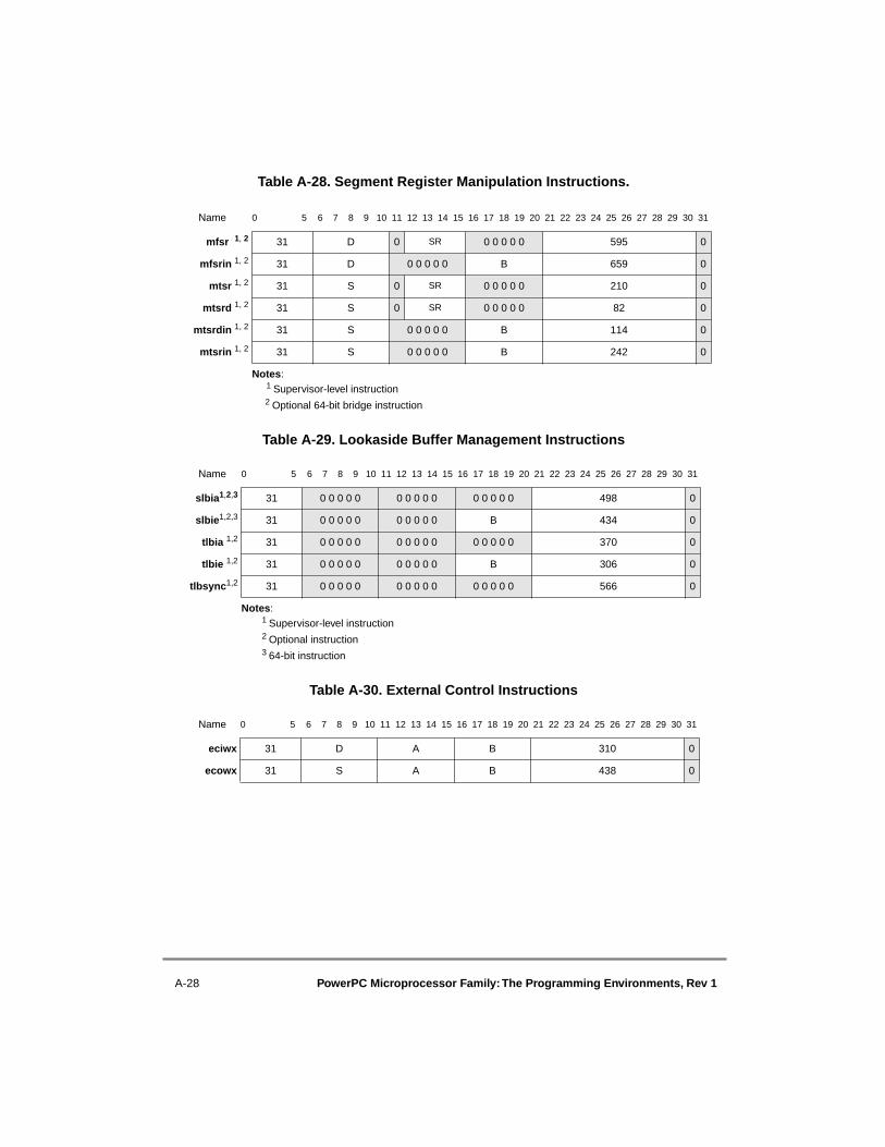
A-28 PowerPC Microprocessor Family: The Programming Environments, Rev 1
Table A-28. Segment Register Manipulation Instructions.
Table A-29. Lookaside Buffer Management Instructions
Table A-30. External Control Instructions
1 Supervisor-level instruction2 Optional 64-bit bridge instruction
1 Supervisor-level instruction2 Optional instruction3 64-bit instruction
Name 0 5 6 7 8 9 10 11 12 13 14 15 16 17 18 19 20 21 22 23 24 25 26 27 28 29 30 31
mfsr 1, 2 31 D 0 SR 0 0 0 0 0 595 0
mfsrin 1, 2 31 D 0 0 0 0 0 B 659 0
mtsr 1, 2 31 S 0 SR 0 0 0 0 0 210 0
mtsrd 1, 2 31 S 0 SR 0 0 0 0 0 82 0
mtsrdin 1, 2 31 S 0 0 0 0 0 B 114 0
mtsrin 1, 2 31 S 0 0 0 0 0 B 242 0
Notes:
Name 0 5 6 7 8 9 10 11 12 13 14 15 16 17 18 19 20 21 22 23 24 25 26 27 28 29 30 31
slbia1,2,3 31 0 0 0 0 0 0 0 0 0 0 0 0 0 0 0 498 0
slbie1,2,3 31 0 0 0 0 0 0 0 0 0 0 B 434 0
tlbia 1,2 31 0 0 0 0 0 0 0 0 0 0 0 0 0 0 0 370 0
tlbie 1,2 31 0 0 0 0 0 0 0 0 0 0 B 306 0
tlbsync1,2 31 0 0 0 0 0 0 0 0 0 0 0 0 0 0 0 566 0
Notes:
Name 0 5 6 7 8 9 10 11 12 13 14 15 16 17 18 19 20 21 22 23 24 25 26 27 28 29 30 31
eciwx 31 D A B 310 0
ecowx 31 S A B 438 0
Appendix A. PowerPC Instruction Set Listings A-29
A.4 Instructions Sorted by FormTable A-31 through Table A-45 list the PowerPC instructions grouped by form.
Table A-31. I-Form
Table A-32. B-Form
Table A-33. SC-Form
Table A-34. D-Form
OPCD LI AA LK
Specific Instruction
Name 0 5 6 7 8 9 10 11 12 13 14 15 16 17 18 19 20 21 22 23 24 25 26 27 28 29 30 31
bx 18 LI AA LK
OPCD BO BI BD AA LK
Specific Instruction
Name 0 5 6 7 8 9 10 11 12 13 14 15 16 17 18 19 20 21 22 23 24 25 26 27 28 29 30 31
bcx 16 BO BI BD AA LK
OPCD 0 0 0 0 0 0 0 0 0 0 0 0 0 0 0 0 0 0 0 0 0 0 0 0 0 1 0
Specific Instruction
Name 0 5 6 7 8 9 10 11 12 13 14 15 16 17 18 19 20 21 22 23 24 25 26 27 28 29 30 31
sc 17 0 0 0 0 0 0 0 0 0 0 0 0 0 0 0 0 0 0 0 0 0 0 0 0 0 1 0
OPCD D A d
OPCD D A SIMM
OPCD S A d
OPCD S A UIMM
OPCD crfD 0 L A SIMM
OPCD crfD 0 L A UIMM
OPCD TO A SIMM
Reserved bits
Key:

A-30 PowerPC Microprocessor Family: The Programming Environments, Rev 1
Specific Instructions
Name 0 5 6 7 8 9 10 11 12 13 14 15 16 17 18 19 20 21 22 23 24 25 26 27 28 29 30 31
addi 14 D A SIMM
addic 12 D A SIMM
addic. 13 D A SIMM
addis 15 D A SIMM
andi. 28 S A UIMM
andis. 29 S A UIMM
cmpi 11 crfD 0 L A SIMM
cmpli 10 crfD 0 L A UIMM
lbz 34 D A d
lbzu 35 D A d
lfd 50 D A d
lfdu 51 D A d
lfs 48 D A d
lfsu 49 D A d
lha 42 D A d
lhau 43 D A d
lhz 40 D A d
lhzu 41 D A d
lmw 1 46 D A d
lwz 32 D A d
lwzu 33 D A d
mulli 7 D A SIMM
ori 24 S A UIMM
oris 25 S A UIMM
stb 38 S A d
stbu 39 S A d
stfd 54 S A d
stfdu 55 S A d
stfs 52 S A d
stfsu 53 S A d
sth 44 S A d
sthu 45 S A d
stmw 1 47 S A d

Appendix A. PowerPC Instruction Set Listings A-31
Table A-35. DS-Form
Table A-36. X-Form
1 Load/store string/multiple instruction2 64-bit instruction
1 64-bit instruction
stw 36 S A d
stwu 37 S A d
subfic 08 D A SIMM
tdi 2 02 TO A SIMM
twi 03 TO A SIMM
xori 26 S A UIMM
xoris 27 S A UIMM
Note:
OPCD D A ds XO
OPCD S A ds XO
Specific Instructions
Name 0 5 6 7 8 9 10 11 12 13 14 15 16 17 18 19 20 21 22 23 24 25 26 27 28 29 30 31
ld 1 58 D A ds 0
ldu 1 58 D A ds 1
lwa 1 58 D A ds 2
std 1 62 S A ds 0
stdu 1 62 S A ds 1
Note:
OPCD D A B XO 0
OPCD D A NB XO 0
OPCD D 0 0 0 0 0 B XO 0
OPCD D 0 0 0 0 0 0 0 0 0 0 XO 0
OPCD D 0 SR 0 0 0 0 0 XO 0
OPCD S A B XO Rc
OPCD S A B XO 1
OPCD S A B XO 0
OPCD S A NB XO 0
OPCD S A 0 0 0 0 0 XO Rc
A-32 PowerPC Microprocessor Family: The Programming Environments, Rev 1
OPCD S 0 0 0 0 0 B XO 0
OPCD S 0 0 0 0 0 0 0 0 0 0 XO 0
OPCD S 0 SR 0 0 0 0 0 XO 0
OPCD S A SH XO Rc
OPCD crfD 0 L A B XO 0
OPCD crfD 0 0 A B XO 0
OPCD crfD 0 0 crfS 0 0 0 0 0 0 0 XO 0
OPCD crfD 0 0 0 0 0 0 0 0 0 0 0 0 XO 0
OPCD crfD 0 0 0 0 0 0 0 IMM 0 XO Rc
OPCD TO A B XO 0
OPCD D 0 0 0 0 0 B XO Rc
OPCD D 0 0 0 0 0 0 0 0 0 0 XO Rc
OPCD crbD 0 0 0 0 0 0 0 0 0 0 XO Rc
OPCD 0 0 0 0 0 A B XO 0
OPCD 0 0 0 0 0 0 0 0 0 0 B XO 0
OPCD 0 0 0 0 0 0 0 0 0 0 0 0 0 0 0 XO 0
Specific Instructions
Name 0 5 6 7 8 9 10 11 12 13 14 15 16 17 18 19 20 21 22 23 24 25 26 27 28 29 30 31
andx 31 S A B 28 Rc
andcx 31 S A B 60 Rc
cmp 31 crfD 0 L A B 0 0
cmpl 31 crfD 0 L A B 32 0
cntlzdx 1 31 S A 0 0 0 0 0 58 Rc
cntlzwx 31 S A 0 0 0 0 0 26 Rc
dcba 2 31 0 0 0 0 0 A B 758 0
dcbf 31 0 0 0 0 0 A B 86 0
dcbi 3 31 0 0 0 0 0 A B 470 0
dcbst 31 0 0 0 0 0 A B 54 0
dcbt 31 0 0 0 0 0 A B 278 0
dcbtst 31 0 0 0 0 0 A B 246 0
dcbz 31 0 0 0 0 0 A B 1014 0
eciwx 31 D A B 310 0
ecowx 31 S A B 438 0
eieio 31 0 0 0 0 0 0 0 0 0 0 0 0 0 0 0 854 0

Appendix A. PowerPC Instruction Set Listings A-33
eqvx 31 S A B 284 Rc
extsbx 31 S A 0 0 0 0 0 954 Rc
extshx 31 S A 0 0 0 0 0 922 Rc
extswx 1 31 S A 0 0 0 0 0 986 Rc
fabsx 63 D 0 0 0 0 0 B 264 Rc
fcfidx 1 63 D 0 0 0 0 0 B 846 Rc
fcmpo 63 crfD 0 0 A B 32 0
fcmpu 63 crfD 0 0 A B 0 0
fctidx 1 63 D 0 0 0 0 0 B 814 Rc
fctidzx 1 63 D 0 0 0 0 0 B 815 Rc
fctiwx 63 D 0 0 0 0 0 B 14 Rc
fctiwzx 63 D 0 0 0 0 0 B 15 Rc
fmrx 63 D 0 0 0 0 0 B 72 Rc
fnabsx 63 D 0 0 0 0 0 B 136 Rc
fnegx 63 D 0 0 0 0 0 B 40 Rc
frspx 63 D 0 0 0 0 0 B 12 Rc
icbi 31 0 0 0 0 0 A B 982 0
lbzux 31 D A B 119 0
lbzx 31 D A B 87 0
ldarx 1 31 D A B 84 0
ldux 1 31 D A B 53 0
ldx 1 31 D A B 21 0
lfdux 31 D A B 631 0
lfdx 31 D A B 599 0
lfsux 31 D A B 567 0
lfsx 31 D A B 535 0
lhaux 31 D A B 375 0
lhax 31 D A B 343 0
lhbrx 31 D A B 790 0
lhzux 31 D A B 311 0
lhzx 31 D A B 279 0
lswi 4 31 D A NB 597 0
lswx 4 31 D A B 533 0
lwarx 31 D A B 20 0
lwaux 1 31 D A B 373 0

A-34 PowerPC Microprocessor Family: The Programming Environments, Rev 1
lwax 1 31 D A B 341 0
lwbrx 31 D A B 534 0
lwzux 31 D A B 55 0
lwzx 31 D A B 23 0
mcrfs 63 crfD 0 0 crfS 0 0 0 0 0 0 0 64 0
mcrxr 31 crfD 0 0 0 0 0 0 0 0 0 0 0 0 512 0
mfcr 31 D 0 0 0 0 0 0 0 0 0 0 19 0
mffsx 63 D 0 0 0 0 0 0 0 0 0 0 583 Rc
mfmsr 3 31 D 0 0 0 0 0 0 0 0 0 0 83 0
mfsr 3, 5 31 D 0 SR 0 0 0 0 0 595 0
mfsrin 3, 5 31 D 0 0 0 0 0 B 659 0
mtfsb0x 63 crbD 0 0 0 0 0 0 0 0 0 0 70 Rc
mtfsb1x 63 crfD 0 0 0 0 0 0 0 0 0 0 38 Rc
mtfsfix 63 crbD 0 0 0 0 0 0 0 IMM 0 134 Rc
mtmsr 3, 5 31 S 0 0 0 0 0 0 0 0 0 0 146 0
mtmsrd 1, 3 31 S 0 0 0 0 0 0 0 0 0 0 178 0
mtsr 3, 5 31 S 0 SR 0 0 0 0 0 210 0
mtsrd 3, 5 31 S 0 SR 0 0 0 0 0 82 0
mtsrin 3, 5 31 S 0 0 0 0 0 B 242 0
mtsrdin 3, 5 31 S 0 0 0 0 0 B 114 0
nandx 31 S A B 476 Rc
norx 31 S A B 124 Rc
orx 31 S A B 444 Rc
orcx 31 S A B 412 Rc
slbia 1,2,3 31 0 0 0 0 0 0 0 0 0 0 0 0 0 0 0 498 0
slbie 1,2,3 31 0 0 0 0 0 0 0 0 0 0 B 434 0
sldx 1 31 S A B 27 Rc
slwx 31 S A B 24 Rc
sradx 1 31 S A B 794 Rc
srawx 31 S A B 792 Rc
srawix 31 S A SH 824 Rc
srdx 1 31 S A B 539 Rc
srwx 31 S A B 536 Rc
stbux 31 S A B 247 0
stbx 31 S A B 215 0

Appendix A. PowerPC Instruction Set Listings A-35
1 64-bit instruction2 Optional instruction3 Supervisor-level instruction4 Load/store string/multiple instruction5 Optional 64-bit bridge instruction
stdcx. 1 31 S A B 214 1
stdux 1 31 S A B 181 0
stdx 1 31 S A B 149 0
stfdux 31 S A B 759 0
stfdx 31 S A B 727 0
stfiwx 2 31 S A B 983 0
stfsux 31 S A B 695 0
stfsx 31 S A B 663 0
sthbrx 31 S A B 918 0
sthux 31 S A B 439 0
sthx 31 S A B 407 0
stswi 4 31 S A NB 725 0
stswx 4 31 S A B 661 0
stwbrx 31 S A B 662 0
stwcx. 31 S A B 150 1
stwux 31 S A B 183 0
stwx 31 S A B 151 0
sync 31 0 0 0 0 0 0 0 0 0 0 0 0 0 0 0 598 0
td 1 31 TO A B 68 0
tlbia 2, 3 31 0 0 0 0 0 0 0 0 0 0 0 0 0 0 0 370 0
tlbie 2, 3 31 0 0 0 0 0 0 0 0 0 0 B 306 0
tlbsync 2, 3 31 0 0 0 0 0 0 0 0 0 0 0 0 0 0 0 566 0
tw 31 TO A B 4 0
xorx 31 S A B 316 Rc
Notes:

A-36 PowerPC Microprocessor Family: The Programming Environments, Rev 1
Table A-37. XL-Form
Table A-38. XFX-Form
1 Supervisor-level instruction2 Optional 64-bit bridge instruction3 64-bit instruction
OPCD BO BI 0 0 0 0 0 XO LK
OPCD crbD crbA crbB XO 0
OPCD crfD 0 0 crfS 0 0 0 0 0 0 0 XO 0
OPCD 0 0 0 0 0 0 0 0 0 0 0 0 0 0 0 XO 0
Specific Instructions
Name 0 5 6 7 8 9 10 11 12 13 14 15 16 17 18 19 20 21 22 23 24 25 26 27 28 29 30 31
bcctrx 19 BO BI 0 0 0 0 0 528 LK
bclrx 19 BO BI 0 0 0 0 0 16 LK
crand 19 crbD crbA crbB 257 0
crandc 19 crbD crbA crbB 129 0
creqv 19 crbD crbA crbB 289 0
crnand 19 crbD crbA crbB 225 0
crnor 19 crbD crbA crbB 33 0
cror 19 crbD crbA crbB 449 0
crorc 19 crbD crbA crbB 417 0
crxor 19 crbD crbA crbB 193 0
isync 19 0 0 0 0 0 0 0 0 0 0 0 0 0 0 0 150 0
mcrf 19 crfD 0 0 crfS 0 0 0 0 0 0 0 0 0
rfi 1,2 19 0 0 0 0 0 0 0 0 0 0 0 0 0 0 0 50 0
rfid 1, 3 19 0 0 0 0 0 0 0 0 0 0 0 0 0 0 0 18 0
Notes:
OPCD D spr XO 0
OPCD D 0 CRM 0 XO 0
OPCD S spr XO 0
OPCD D tbr XO 0
Specific Instructions
Name 0 5 6 7 8 9 10 11 12 13 14 15 16 17 18 19 20 21 22 23 24 25 26 27 28 29 30 31
mfspr 1 31 D spr 339 0
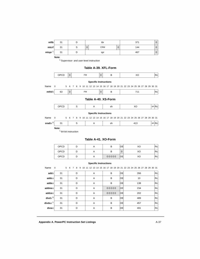
Appendix A. PowerPC Instruction Set Listings A-37
Table A-39. XFL-Form
Table A-40. XS-Form
Table A-41. XO-Form
1 Supervisor- and user-level instruction
1 64-bit instruction
mftb 31 D tbr 371 0
mtcrf 31 S 0 CRM 0 144 0
mtspr 1 31 D spr 467 0
Note:
OPCD 0 FM 0 B XO Rc
Specific Instructions
Name 0 5 6 7 8 9 10 11 12 13 14 15 16 17 18 19 20 21 22 23 24 25 26 27 28 29 30 31
mtfsfx 63 0 FM 0 B 711 Rc
OPCD S A sh XO sh Rc
Specific Instructions
Name 0 5 6 7 8 9 10 11 12 13 14 15 16 17 18 19 20 21 22 23 24 25 26 27 28 29 30 31
sradix 1 31 S A sh 413 sh Rc
Note:
OPCD D A B OE XO Rc
OPCD D A B 0 XO Rc
OPCD D A 0 0 0 0 0 OE XO Rc
Specific Instructions
Name 0 5 6 7 8 9 10 11 12 13 14 15 16 17 18 19 20 21 22 23 24 25 26 27 28 29 30 31
addx 31 D A B OE 266 Rc
addcx 31 D A B OE 10 Rc
addex 31 D A B OE 138 Rc
addmex 31 D A 0 0 0 0 0 OE 234 Rc
addzex 31 D A 0 0 0 0 0 OE 202 Rc
divdx 1 31 D A B OE 489 Rc
divdux 1 31 D A B OE 457 Rc
divwx 31 D A B OE 491 Rc

A-38 PowerPC Microprocessor Family: The Programming Environments, Rev 1
Table A-42. A-Form
1 64-bit instruction
divwux 31 D A B OE 459 Rc
mulhdx 1 31 D A B 0 73 Rc
mulhdux 1 31 D A B 0 9 Rc
mulhwx 31 D A B 0 75 Rc
mulhwux 31 D A B 0 11 Rc
mulldx 1 31 D A B OE 233 Rc
mullwx 31 D A B OE 235 Rc
negx 31 D A 0 0 0 0 0 OE 104 Rc
subfx 31 D A B OE 40 Rc
subfcx 31 D A B OE 8 Rc
subfex 31 D A B OE 136 Rc
subfmex 31 D A 0 0 0 0 0 OE 232 Rc
subfzex 31 D A 0 0 0 0 0 OE 200 Rc
Note:
OPCD D A B 0 0 0 0 0 XO Rc
OPCD D A B C XO Rc
OPCD D A 0 0 0 0 0 C XO Rc
OPCD D 0 0 0 0 0 B 0 0 0 0 0 XO Rc
Specific Instructions
Name 0 5 6 7 8 9 10 11 12 13 14 15 16 17 18 19 20 21 22 23 24 25 26 27 28 29 30 31
faddx 63 D A B 0 0 0 0 0 21 Rc
faddsx 59 D A B 0 0 0 0 0 21 Rc
fdivx 63 D A B 0 0 0 0 0 18 Rc
fdivsx 59 D A B 0 0 0 0 0 18 Rc
fmaddx 63 D A B C 29 Rc
fmaddsx 59 D A B C 29 Rc
fmsubx 63 D A B C 28 Rc
fmsubsx 59 D A B C 28 Rc
fmulx 63 D A 0 0 0 0 0 C 25 Rc
fmulsx 59 D A 0 0 0 0 0 C 25 Rc
fnmaddx 63 D A B C 31 Rc
fnmaddsx 59 D A B C 31 Rc
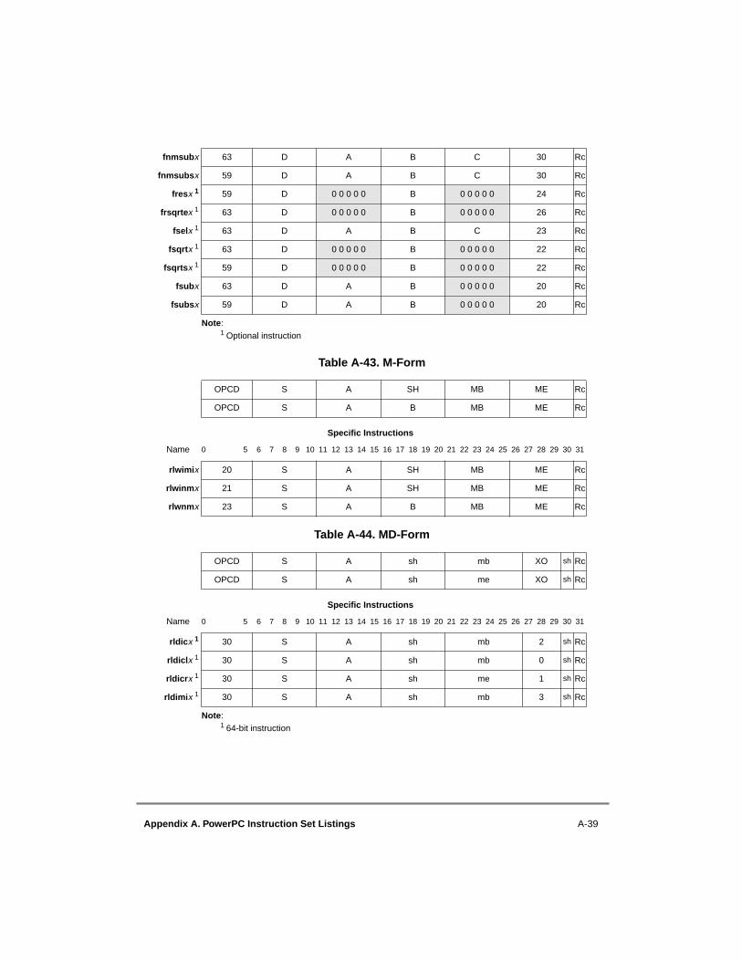
Appendix A. PowerPC Instruction Set Listings A-39
Table A-43. M-Form
Table A-44. MD-Form
1 Optional instruction
1 64-bit instruction
fnmsubx 63 D A B C 30 Rc
fnmsubsx 59 D A B C 30 Rc
fresx 1 59 D 0 0 0 0 0 B 0 0 0 0 0 24 Rc
frsqrtex 1 63 D 0 0 0 0 0 B 0 0 0 0 0 26 Rc
fselx 1 63 D A B C 23 Rc
fsqrtx 1 63 D 0 0 0 0 0 B 0 0 0 0 0 22 Rc
fsqrtsx 1 59 D 0 0 0 0 0 B 0 0 0 0 0 22 Rc
fsubx 63 D A B 0 0 0 0 0 20 Rc
fsubsx 59 D A B 0 0 0 0 0 20 Rc
Note:
OPCD S A SH MB ME Rc
OPCD S A B MB ME Rc
Specific Instructions
Name 0 5 6 7 8 9 10 11 12 13 14 15 16 17 18 19 20 21 22 23 24 25 26 27 28 29 30 31
rlwimix 20 S A SH MB ME Rc
rlwinmx 21 S A SH MB ME Rc
rlwnmx 23 S A B MB ME Rc
OPCD S A sh mb XO sh Rc
OPCD S A sh me XO sh Rc
Specific Instructions
Name 0 5 6 7 8 9 10 11 12 13 14 15 16 17 18 19 20 21 22 23 24 25 26 27 28 29 30 31
rldicx 1 30 S A sh mb 2 sh Rc
rldiclx 1 30 S A sh mb 0 sh Rc
rldicrx 1 30 S A sh me 1 sh Rc
rldimix 1 30 S A sh mb 3 sh Rc
Note:
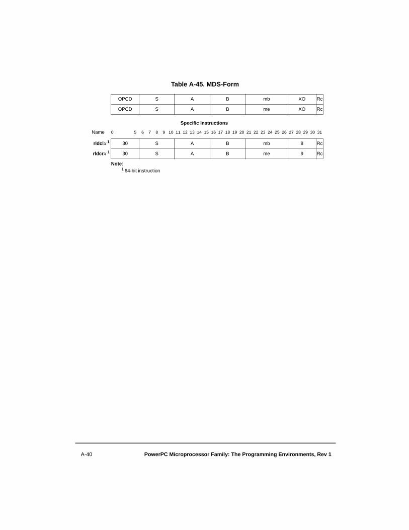
A-40 PowerPC Microprocessor Family: The Programming Environments, Rev 1
Table A-45. MDS-Form
1 64-bit instruction
OPCD S A B mb XO Rc
OPCD S A B me XO Rc
Specific Instructions
Name 0 5 6 7 8 9 10 11 12 13 14 15 16 17 18 19 20 21 22 23 24 25 26 27 28 29 30 31
rldclx 1 30 S A B mb 8 Rc
rldcrx 1 30 S A B me 9 Rc
Note:

Appendix A. PowerPC Instruction Set Listings A-41
A.5 Instruction Set LegendTable A-46 provides general information on the PowerPC instruction set (such as thearchitectural level, privilege level, and form).
Table A-46. PowerPC Instruction Set Legend
UISA VEA OEASupervisor
Level64-Bit Only
64-Bit Bridge
Optional Form
addx √ XO
addcx √ XO
addex √ XO
addi √ D
addic √ D
addic. √ D
addis √ D
addmex √ XO
addzex √ XO
andx √ X
andcx √ X
andi. √ D
andis. √ D
bx √ I
bcx √ B
bcctrx √ XL
bclrx √ XL
cmp √ X
cmpi √ D
cmpl √ X
cmpli √ D
cntlzdx √ √ X
cntlzwx √ X
crand √ XL
crandc √ XL
creqv √ XL
crnand √ XL
crnor √ XL
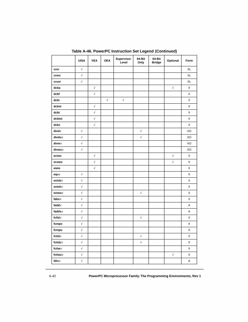
A-42 PowerPC Microprocessor Family: The Programming Environments, Rev 1
cror √ XL
crorc √ XL
crxor √ XL
dcba √ √ X
dcbf √ X
dcbi √ √ X
dcbst √ X
dcbt √ X
dcbtst √ X
dcbz √ X
divdx √ √ XO
divdux √ √ XO
divwx √ XO
divwux √ XO
eciwx √ √ X
ecowx √ √ X
eieio √ X
eqvx √ X
extsbx √ X
extshx √ X
extswx √ √ X
fabsx √ X
faddx √ A
faddsx √ A
fcfidx √ √ X
fcmpo √ X
fcmpu √ X
fctidx √ √ X
fctidzx √ √ X
fctiwx √ X
fctiwzx √ √ X
fdivx √ A
Table A-46. PowerPC Instruction Set Legend (Continued)
UISA VEA OEASupervisor
Level64-Bit Only
64-Bit Bridge
Optional Form
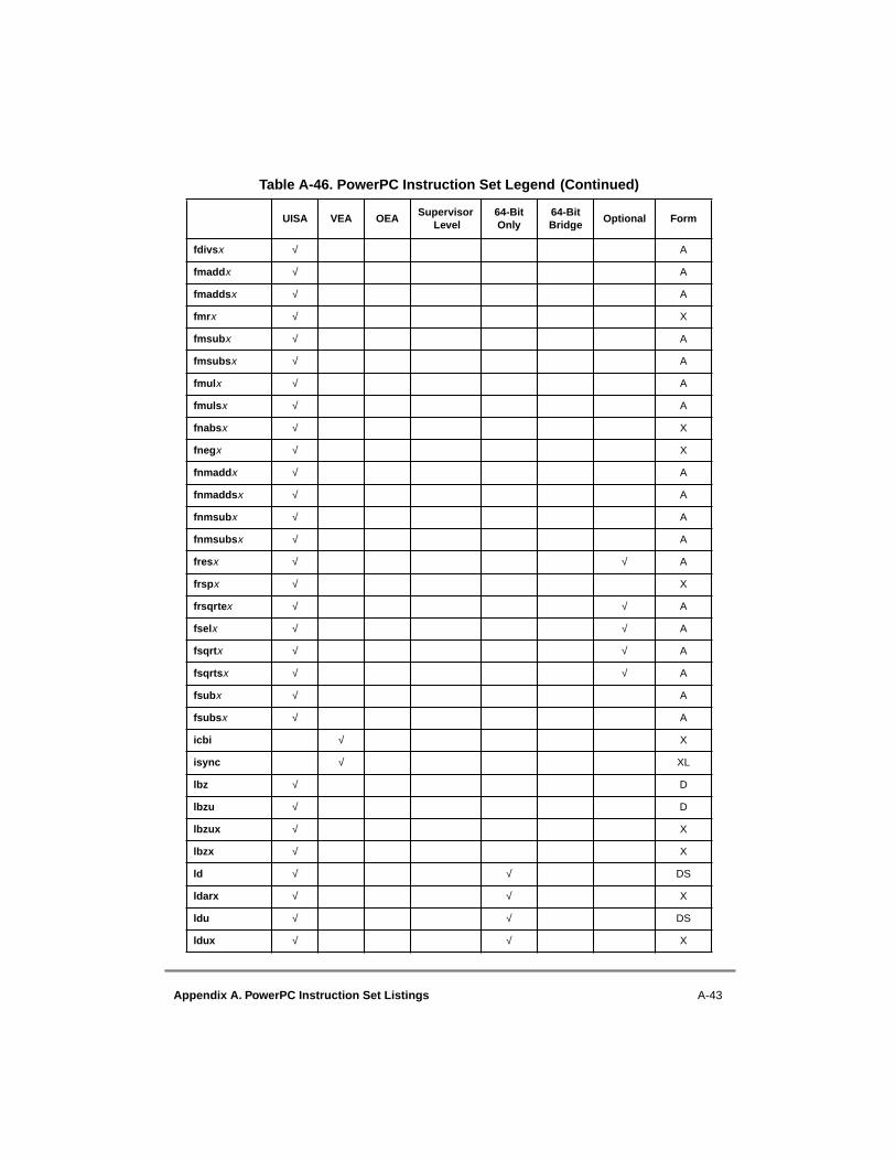
Appendix A. PowerPC Instruction Set Listings A-43
fdivsx √ A
fmaddx √ A
fmaddsx √ A
fmrx √ X
fmsubx √ A
fmsubsx √ A
fmulx √ A
fmulsx √ A
fnabsx √ X
fnegx √ X
fnmaddx √ A
fnmaddsx √ A
fnmsubx √ A
fnmsubsx √ A
fresx √ √ A
frspx √ X
frsqrtex √ √ A
fselx √ √ A
fsqrtx √ √ A
fsqrtsx √ √ A
fsubx √ A
fsubsx √ A
icbi √ X
isync √ XL
lbz √ D
lbzu √ D
lbzux √ X
lbzx √ X
ld √ √ DS
ldarx √ √ X
ldu √ √ DS
ldux √ √ X
Table A-46. PowerPC Instruction Set Legend (Continued)
UISA VEA OEASupervisor
Level64-Bit Only
64-Bit Bridge
Optional Form
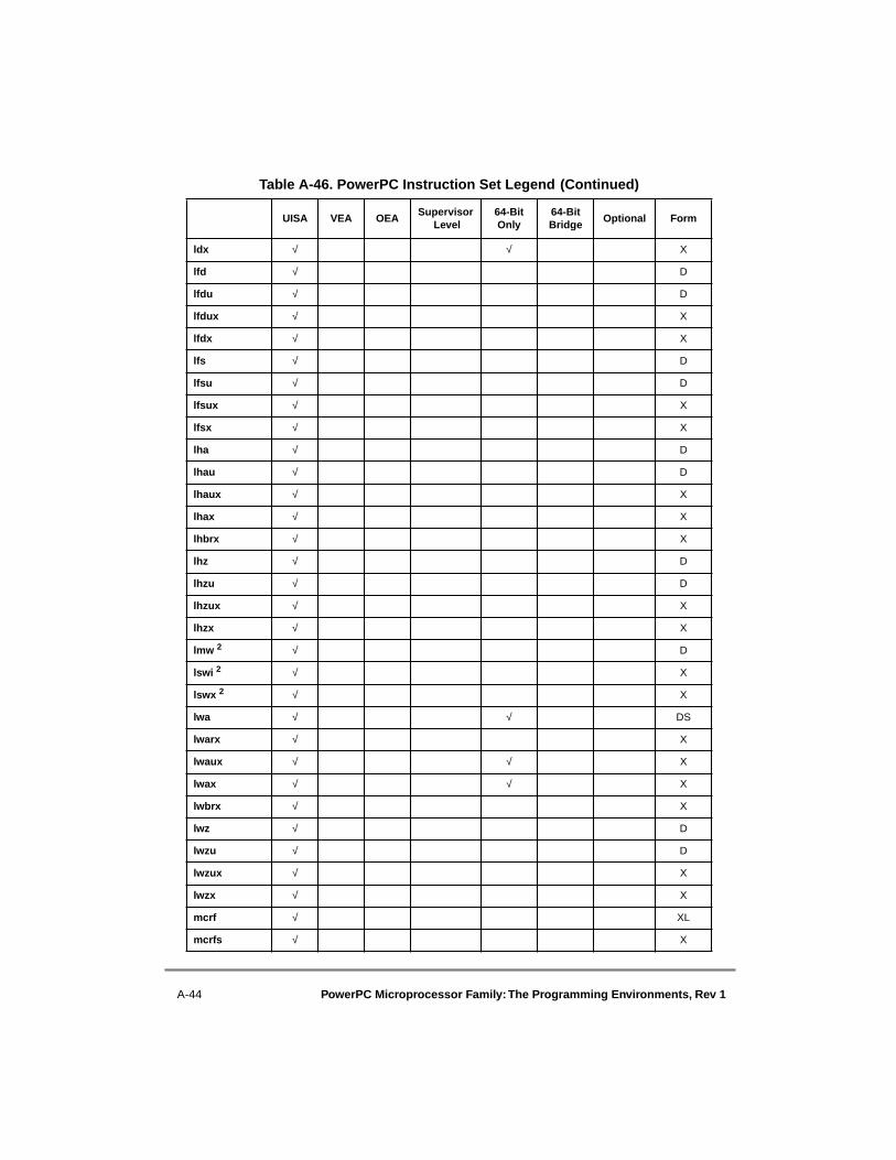
A-44 PowerPC Microprocessor Family: The Programming Environments, Rev 1
ldx √ √ X
lfd √ D
lfdu √ D
lfdux √ X
lfdx √ X
lfs √ D
lfsu √ D
lfsux √ X
lfsx √ X
lha √ D
lhau √ D
lhaux √ X
lhax √ X
lhbrx √ X
lhz √ D
lhzu √ D
lhzux √ X
lhzx √ X
lmw 2 √ D
lswi 2 √ X
lswx 2 √ X
lwa √ √ DS
lwarx √ X
lwaux √ √ X
lwax √ √ X
lwbrx √ X
lwz √ D
lwzu √ D
lwzux √ X
lwzx √ X
mcrf √ XL
mcrfs √ X
Table A-46. PowerPC Instruction Set Legend (Continued)
UISA VEA OEASupervisor
Level64-Bit Only
64-Bit Bridge
Optional Form

Appendix A. PowerPC Instruction Set Listings A-45
mcrxr √ X
mfcr √ X
mffs √ X
mfmsr √ √ X
mfspr 1 √ √ √ XFX
mfsr √ √ √ √ X
mfsrin √ √ √ √ X
mftb √ XFX
mtcrf √ XFX
mtfsb0x √ X
mtfsb1x √ X
mtfsfx √ XFL
mtfsfix √ X
mtmsr √ √ √ √ X
mtmsrd √ √ √ X
mtspr 1 √ √ √ XFX
mtsr √ √ √ √ X
mtsrd √ √ √ √ √ X
mtsrdin √ √ √ √ √ X
mtsrin √ √ √ √ X
mulhdx √ √ XO
mulhdux √ √ XO
mulhwx √ XO
mulhwux √ XO
mulldx √ √ XO
mulli √ D
mullwx √ XO
nandx √ X
negx √ XO
norx √ X
orx √ X
orcx √ X
Table A-46. PowerPC Instruction Set Legend (Continued)
UISA VEA OEASupervisor
Level64-Bit Only
64-Bit Bridge
Optional Form

A-46 PowerPC Microprocessor Family: The Programming Environments, Rev 1
ori √ D
oris √ D
rfi √ √ √ √ √ XL
rfid √ √ √ XL
rldclx √ √ MDS
rldcrx √ √ MDS
rldicx √ √ MD
rldiclx √ √ MD
rldicrx √ √ MD
rldimix √ √ MD
rlwimix √ M
rlwinmx √ M
rlwnmx √ M
sc √ √ SC
slbia √ √ √ √ X
slbie √ √ √ √ X
sldx √ √ X
slwx √ X
sradx √ √ X
sradix √ √ XS
srawx √ X
srawix √ X
srdx √ √ X
srwx √ X
stb √ D
stbu √ D
stbux √ X
stbx √ X
std √ √ DS
stdcx. √ √ X
stdu √ √ DS
stdux √ √ X
Table A-46. PowerPC Instruction Set Legend (Continued)
UISA VEA OEASupervisor
Level64-Bit Only
64-Bit Bridge
Optional Form
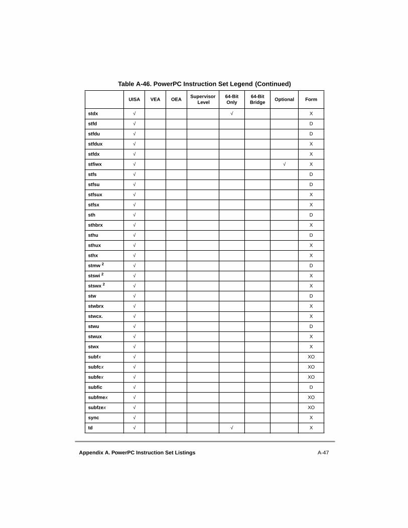
Appendix A. PowerPC Instruction Set Listings A-47
stdx √ √ X
stfd √ D
stfdu √ D
stfdux √ X
stfdx √ X
stfiwx √ √ X
stfs √ D
stfsu √ D
stfsux √ X
stfsx √ X
sth √ D
sthbrx √ X
sthu √ D
sthux √ X
sthx √ X
stmw 2 √ D
stswi 2 √ X
stswx 2 √ X
stw √ D
stwbrx √ X
stwcx. √ X
stwu √ D
stwux √ X
stwx √ X
subfx √ XO
subfcx √ XO
subfex √ XO
subfic √ D
subfmex √ XO
subfzex √ XO
sync √ X
td √ √ X
Table A-46. PowerPC Instruction Set Legend (Continued)
UISA VEA OEASupervisor
Level64-Bit Only
64-Bit Bridge
Optional Form

A-48 PowerPC Microprocessor Family: The Programming Environments, Rev 1
1 Supervisor- and user-level instruction2 Load/store string or multiple instruction
tdi √ √ D
tlbiax √ √ √ X
tlbiex √ √ √ X
tlbsync √ √ X
tw √ X
twi √ D
xorx √ X
xori √ D
xoris √ D
Notes:
Table A-46. PowerPC Instruction Set Legend (Continued)
UISA VEA OEASupervisor
Level64-Bit Only
64-Bit Bridge
Optional Form
Appendix B. POWER Architecture Cross Reference B-1
Appendix BPOWER Architecture Cross ReferenceB0B0
This appendix identifies the incompatibilities that must be managed in migration from thePOWER architecture to PowerPC architecture. Some of the incompatibilities can, at leastin principle, be detected by the processor, which traps and lets software simulate thePOWER operation. Others cannot be detected by the processor.
In general, the incompatibilities identified here are those that affect a POWER applicationprogram. Incompatibilities for instructions that can be used only by POWER systemprograms are not discussed. Note that this appendix describes incompatibilities withrespect to the PowerPC architecture in general.
B.1 New Instructions, Formerly Supervisor-Level Instructions
Instructions new to PowerPC typically use opcode values (including extended opcode) thatare illegal in the POWER architecture. A few instructions that are supervisor-level in thePOWER architecture (for example, dclz, called dcbz in the PowerPC architecture) havebeen made user-level in the PowerPC architecture. Any POWER program that executes oneof these now-valid, or now-user-level, instructions expecting to cause the system illegalinstruction error handler (program exception) or the system supervisor-level instructionerror handler to be invoked, will not execute correctly on PowerPC processors. (Note that,in the architecture specification, user- and supervisor-level are referred to as problem andprivileged state, respectively, and exceptions are referred to as interrupts.)
B.2 New Supervisor-Level InstructionsThe following instructions are user-level in the POWER architecture but are supervisor-level in PowerPC processors.
• mfmsr
• mfsr

B-2 PowerPC Microprocessor Family: The Programming Environments, Rev. 1
B.3 Reserved Bits in InstructionsThese are shown as zeros and the bit field is shaded in the instruction opcode definitions.In the POWER architecture such bits are ignored by the processor. In the PowerPCarchitecture they must be zero or the instruction form is invalid. In several cases, thePowerPC architecture assumes that such bits in POWER instructions are indeed zero. Thecases include the following:
• cmpi, cmp, cmpli, and cmpl assume that bit 10 in the POWER instructions is 0.
• mtspr and mfspr assume that bits 16–20 in the POWER instructions are 0.
B.4 Reserved Bits in RegistersThe POWER architecture defines these bits to be zero when read, and either zero or onewhen written to. In the PowerPC architecture it is implementation-dependent for eachregister, whether these bits are zero when read, and ignored when written to, or are copiedfrom source to destination when read or written to.
B.5 Alignment CheckThe AL bit in the POWER machine state register, MSR[24], is not supported in thePowerPC architecture. The bit is reserved in the PowerPC architecture. The low-order bitsof the EA are always used. Notice that value zero—the normal value for a reserved SPRbit—means ignore the low-order EA bits in the POWER architecture, and value one meansuse the low-order EA bits. However, MSR[24] is not assigned new meaning in the PowerPCarchitecture.
B.6 Condition RegisterThe following instructions specify a field in the condition register (CR) explicitly (via thecrfD field) and also have the record bit (Rc) option. In the PowerPC architecture, if Rc = 1for these instructions the instruction form is invalid. In the POWER architecture, if Rc = 1the instructions execute normally except as shown in Table B-1.
Table B-1. Condition Register Settings
Instruction Setting
cmp CR0 is undefined if Rc = 1 and crfD ≠ 0
cmpl CR0 is undefined if Rc = 1 and crfD ≠ 0
mcrxr CR0 is undefined if Rc = 1 and crfD ≠ 0
fcmpu CR1 is undefined if Rc = 1
fcmpo CR1 is undefined if Rc = 1
mcrfs CR1 is undefined if Rc = 1 and crfD ≠ 1
Appendix B. POWER Architecture Cross Reference B-3
B.7 Inappropriate Use of LK and Rc bits For the instructions listed below, if LK = 1 or Rc = 1, POWER processors execute theinstruction normally with the exception of setting the link register (if LK = 1) or the CR0or CR1 fields (if Rc = 1) to an undefined value. In the PowerPC architecture, suchinstruction forms are invalid.
The PowerPC instruction form is invalid if LK = 1:
• sc (svcx in the POWER architecture)
• Condition register logical instructions (that is, crand, crandc, creqv, crnand, crnor, cror, crorc, and crxor)
• mcrf
• isync (ics in the POWER architecture)
The PowerPC instruction form is invalid if Rc = 1:
• Integer X-form load and store instructions:
— X-form load instructions—lbzux, lbzx, ldarx, ldux, ldx, lhaux, lhax, lhbrx, lhzux, lhzx, lswi, lswx, lwarx, lwaux, lwax, lwbrx, lwzux, lwzx
— X-form store instructions—stbux, stbx, stdcx., stdux, stdx, sthbrx, sthux, sthx, stswi, stswx, stwbrx, stwcx., stwux, stwx
• Integer X-form compare instructions (that is, cmp, cmpl)
• X-form trap instruction (that is, td)
• mtspr, mfspr, mtcrf, mcrxr, mfcr
• Floating-point X-form load and store instructions and floating-point compare instructions
— Floating-point X-form load instructions— lfdux, lfdx, lfsux, lfsx
— Floating-point X-form store instructions—stfdux, stfdx, stfiwx, stfsux, stfsx
— Floating-point X-form compare instruction—fcmpo, fcmpu
• mcrfs
• dcbz (dclz in the POWER architecture)
B.8 BO FieldThe POWER architecture shows certain bits in the BO field—used by branch conditionalinstructions—as x without indicating how these bits are to be interpreted. These bits areignored by POWER processors.
The PowerPC architecture shows these bits as either z or y. The z bits are ignored, as inPOWER. However, the y bit need not be ignored, but rather can be used to give a hint aboutwhether the branch is likely to be taken. If a POWER program has the incorrect value forthis bit, the program will run correctly but performance may suffer.

B-4 PowerPC Microprocessor Family: The Programming Environments, Rev. 1
B.9 Branch Conditional to Count RegisterFor the case in which the count register is decremented and tested (that is, the case in whichBO[2] = 0), the POWER architecture specifies only that the branch target address isundefined, implying that the count register, and the link register (if LK = 1), are updated inthe normal way. The PowerPC architecture considers this instruction form invalid.
B.10 System Call/Supervisor CallThe System Call (sc) instruction in the PowerPC architecture is called Supervisor Call(svcx) in the POWER architecture. Differences in implementations are as follows:
• The POWER architecture provides a version of the svcx instruction (bit 30 = 0) that allows instruction fetching to continue at any one of 128 locations. It is used for “fast Supervisor Calls.” The PowerPC architecture provides no such version. If bit 30 of the instruction is zero the instruction form is invalid.
• The POWER architecture provides a version of the svcx instruction (bits 30–31 = 0b11) that resumes instruction fetching at one location and sets the link register (LR) to the address of the next instruction. The PowerPC architecture provides no such version; if Rc = 1, the instruction form is invalid.
• For the POWER architecture, information from the MSR is saved in the count register (CTR). For the PowerPC architecture, this information is saved in the machine status save/restore register 1 (SRR1).
• The POWER architecture permits bits 16–29 of the instruction to be nonzero, while in the PowerPC architecture, such an instruction form is invalid.
• The POWER architecture saves the low-order 16 bits of the svcx instruction in the CTR; the PowerPC architecture does not save them.
• The settings of the MSR bits by the system call exception differ between the POWER architecture and the PowerPC architecture.
B.11 XER RegisterBits 16–23 of the XER are reserved in the PowerPC architecture, whereas in the POWERarchitecture they are defined to contain the comparison byte for the lscbx instruction, whichis not included in the PowerPC architecture.
B.12 Update Forms of Memory AccessThe PowerPC architecture requires that rA not be equal to either rD (integer load only) orzero. If the restriction is violated, the instruction form is invalid. See Section 4.1.3, “Classesof Instructions,” for information about invalid instructions. The POWER architecturepermits these cases and simply avoids saving the EA.

Appendix B. POWER Architecture Cross Reference B-5
B.13 Multiple Register LoadsWhen executing instructions that load multiple registers, the PowerPC architecture requiresthat rA, and rB if present in the instruction format, not be in the range of registers to beloaded, while the POWER architecture permits this and does not alter rA or rB in this case.(The PowerPC architecture restriction applies even if rA = 0, although there is no obviousbenefit to the restriction in this case since rA is not used to compute the effective addressif rA = 0.) If the PowerPC architecture restriction is violated, either the system illegalinstruction error handler is invoked or the results are boundedly undefined.
The instructions affected are listed as follows:
• lmw (lm in the POWER architecture)
• lswi (lsi in the POWER architecture)
• lswx (lsx in the POWER architecture)
For example, an lmw instruction that loads all 32 registers is valid in the POWERarchitecture but is an invalid form in the PowerPC architecture.
B.14 Alignment for Load/Store MultipleWhen executing load/store multiple instructions, the PowerPC architecture requires the EAto be word-aligned and yields an alignment exception or boundedly-undefined results if itis not. The POWER architecture specifies that an alignment exception occurs (if AL = 1).
B.15 Load and Store String InstructionsIn the PowerPC architecture, an lswx instruction with zero length leaves the content of rDundefined (if rD ≠ rA and rD ≠ rB) or is an invalid instruction form (if rD = rA or rD = rB), while in the POWER architecture the corresponding instruction (lsx) is a no-opin these cases.
Note also that, in the PowerPC architecture, an lswx instruction with zero length may alterthe referenced bit, and an stswx instruction with zero length may alter the referenced andchanged bits, while in the POWER architecture the corresponding instructions (lsx andstsx) do not alter the referenced and changed bits.
B.16 Synchronization The sync instruction (called dcs in the POWER architecture) and the isync instruction(called the ics in the POWER architecture) cause a much more pervasive synchronizationin the PowerPC architecture than in the POWER architecture. For more information, referto Chapter 8, “Instruction Set.”
B-6 PowerPC Microprocessor Family: The Programming Environments, Rev. 1
B.17 Move to/from SPRDifferences in how the Move to/from Special Purpose Register (mtspr and mfspr)instructions function are as follows:
• The SPR field is 10 bits long in the PowerPC architecture, but only 5 bits in POWER architecture.
• The mfspr instruction can be used to read the decrementer (DEC) register in problem state (user mode) in the POWER architecture, but only in supervisor state in the PowerPC architecture.
• If the SPR value specified in the instruction is not one of the defined values, the POWER architecture behaves as follows:
— If the instruction is executed in user-level privilege state and SPR[0] = 1, a supervisor-level instruction type program exception occurs. No architected registers are altered except those set by the exception.
— If the instruction is executed in supervisor-level privilege state and SPR[0] = 0, no architected registers are altered.
In this same case, the PowerPC architecture behaves as follows:— If the instruction is executed in user-level privilege state and SPR[0] = 1, either
an illegal instruction type program exception or a supervisor-level instruction type program exception occurs. No architected registers are altered except those set by the exception.
— Otherwise, (the instruction is executed in supervisor-level privilege state or SPR[0] = 0), either an illegal instruction type program exception occurs (in which case no architected registers are altered except those set by the exception) or the results are boundedly undefined.
B.18 Effects of Exceptions on FPSCR Bits FR and FIFor the following cases, the POWER architecture does not specify how the FR and FI bitsare set, while the PowerPC architecture preserves them for illegal operation exceptionscaused by compare instructions and clears them otherwise.
• Invalid operation exception (enabled or disabled)
• Zero divide exception (enabled or disabled)
• Disabled overflow exception
Appendix B. POWER Architecture Cross Reference B-7
B.19 Floating-Point Store Single InstructionsThere are several respects in which the PowerPC architecture is incompatible with thePOWER architecture when executing store floating-point single instructions.
The POWER architecture uses FPSCR[UE] to help determine whether denormalizationshould be done, while the PowerPC architecture does not. Note that in the PowerPCarchitecture, if FPSCR[UE] = 1 and a denormalized single-precision number is copied fromone memory location to another by means of an lfs instruction followed by an stfsinstruction, the two “copies” may not be the same. Refer to Section 3.3.6.2.2, “UnderflowException Condition,” for more information about underflow exceptions.
For an operand having an exponent that is less than 874 (an unbiased exponent less than -149), the POWER architecture specifies storage of a zero (if FPSCR[UE] = 0), while thePowerPC architecture specifies the storage of an undefined value.
B.20 Move from FPSCRThe POWER architecture defines the high-order 32 bits of the result of mffs to be 0xFFFF_FFFF. In the PowerPC architecture they are undefined.
B.21 Clearing Bytes in the Data CacheThe dclz instruction of the POWER architecture and the dcbz instruction of the PowerPCarchitecture have the same opcode. However, the functions differ in the following respects.
• The dclz instruction clears a line; dcbz clears a block.
• The dclz instruction saves the EA in rA (if rA ≠ 0); dcbz does not.
• The dclz instruction is supervisor-level; dcbz is not.
B.22 Segment Register InstructionsThe definitions of the four segment register instructions (mtsr, mtsrin, mfsr, and mfsrin)differ in two respects between the POWER architecture and the PowerPC architecture.Instructions similar to mtsrin and mfsrin are called mtsri and mfsri in the POWERarchitecture. The definitions follow:
• Privilege—mfsr and mfsri are problem state instructions in the POWER architecture, while mfsr and mfsrin are supervisor-level in the PowerPC architecture.
• Function—the indirect instructions (mtsri and mfsri) in the POWER architecture use an rA register in computing the segment register number, and the computed EA is stored into rA (if rA ≠ 0 and rA ≠ rD); in the PowerPC architecture mtsrin and mfsrin have no rA field and EA is not stored.

B-8 PowerPC Microprocessor Family: The Programming Environments, Rev. 1
The mtsr, mtsrin (mtsri), and mfsr instructions have the same opcodes in the PowerPCarchitecture as in the POWER architecture. The mfsri instruction in the POWERarchitecture and the mfsrin instruction in PowerPC architecture have different opcodes.
B.23 TLB Entry InvalidationThe tlbi instruction in the POWER architecture and the tlbie instruction in the PowerPCarchitecture have the same opcode. However, the functions differ in the following respects.
• The tlbi instruction computes the EA as (rA|0) + rB, while tlbie lacks an rA field and computes the EA as rB.
• The tlbi instruction saves the EA in rA (if rA ≠ 0); tlbie lacks an rA field and does not save the EA.
B.24 Floating-Point ExceptionsBoth the PowerPC and the POWER architectures use bit 20 of the MSR to control thegeneration of exceptions for floating-point enabled exceptions. However, in the PowerPCarchitecture this bit is part of a 2-bit value which controls the occurrence, precision, andrecoverability of the exception, whereas, in the POWER architecture this bit is usedindependently to control the occurrence of the exception (in the POWER architecture allfloating-point exceptions are precise).
B.25 Timing FacilitiesThis section describes differences between the POWER architecture and the PowerPCarchitecture timer facilities.
B.25.1 Real-Time ClockThe POWER real-time clock (RTC) is not supported in the PowerPC architecture. Instead,the PowerPC architecture provides a time base register (TB). Both the RTC and the TB are64-bit special-purpose registers, but they differ in the following respects:
• The RTC counts seconds and nanoseconds, while the TB counts ticks. The frequency of the TB is implementation-dependent.
• The RTC increments discontinuously—1 is added to RTCU when the value in RTCL passes 999_999_999. The TB increments continuously—1 is added to TBU when the value in TBL passes 0xFFFF_FFFF.
• The RTC is written and read by the mtspr and mfspr instructions, using SPR numbers that denote the RTCU and RTCD. The TB is written by the mtspr instruction (using new SPR numbers) and read by the new mftb instruction.
• The SPR numbers that denote POWER architectures’s RTCL and RTCU are invalid in the PowerPC architecture.

Appendix B. POWER Architecture Cross Reference B-9
• The RTC is guaranteed to increment at least once in the time required to execute ten Add Immediate (addi) instructions. No analogous guarantee is made for the TB.
• Not all bits of RTCL need be implemented, while all bits of the TB must be implemented.
B.25.2 DecrementerThe decrementer (DEC) register differs, in the PowerPC and POWER architectures, in thefollowing respects:
• The PowerPC architecture DEC register decrements at the same rate that the TB increments, while the POWER decrementer decrements every nanosecond (which is the same rate that the RTC increments).
• Not all bits of the POWER DEC need be implemented, while all bits of the PowerPC DEC must be implemented.
• The exception caused by the DEC has its own exception vector location in the PowerPC architecture, but is considered an external exception in the POWER architecture.
B.26 Deleted InstructionsThe following instructions, shown in Table B-2, are part of the POWER architecture buthave been dropped from the PowerPC architecture.
Table B-2. Deleted POWER Instructions
Mnemonic InstructionPrimary Opcode
Extended Opcode
abs Absolute 31 360
clcs Cache Line Compute Size 31 531
clf Cache Line Flush 31 118
cli Cache Line Invalidate 31 502
dclst Data Cache Line Store 31 630
div Divide 31 331
divs Divide Short 31 363
doz Difference or Zero 31 264
dozi Difference or Zero Immediate 09 —
lscbx Load String and Compare Byte Indexed 31 277
maskg Mask Generate 31 29
maskir Mask Insert from Register 31 541
mfsrin Move from Segment Register Indirect 31 627
mul Multiply 31 107
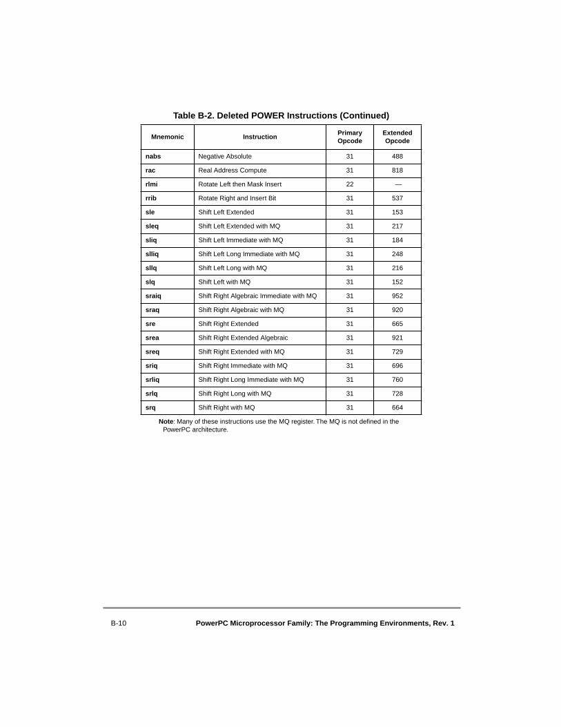
B-10 PowerPC Microprocessor Family: The Programming Environments, Rev. 1
nabs Negative Absolute 31 488
rac Real Address Compute 31 818
rlmi Rotate Left then Mask Insert 22 —
rrib Rotate Right and Insert Bit 31 537
sle Shift Left Extended 31 153
sleq Shift Left Extended with MQ 31 217
sliq Shift Left Immediate with MQ 31 184
slliq Shift Left Long Immediate with MQ 31 248
sllq Shift Left Long with MQ 31 216
slq Shift Left with MQ 31 152
sraiq Shift Right Algebraic Immediate with MQ 31 952
sraq Shift Right Algebraic with MQ 31 920
sre Shift Right Extended 31 665
srea Shift Right Extended Algebraic 31 921
sreq Shift Right Extended with MQ 31 729
sriq Shift Right Immediate with MQ 31 696
srliq Shift Right Long Immediate with MQ 31 760
srlq Shift Right Long with MQ 31 728
srq Shift Right with MQ 31 664
Note: Many of these instructions use the MQ register. The MQ is not defined in the PowerPC architecture.
Table B-2. Deleted POWER Instructions (Continued)
Mnemonic InstructionPrimary Opcode
Extended Opcode
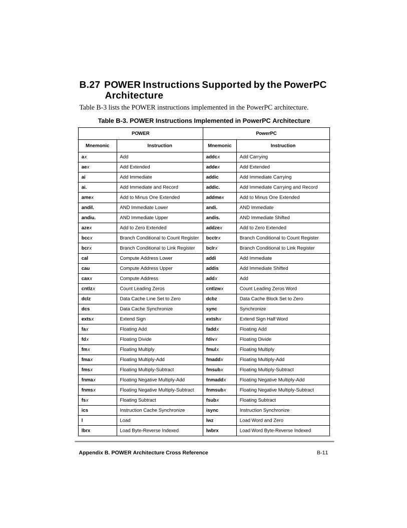
Appendix B. POWER Architecture Cross Reference B-11
B.27 POWER Instructions Supported by the PowerPC Architecture
Table B-3 lists the POWER instructions implemented in the PowerPC architecture.
Table B-3. POWER Instructions Implemented in PowerPC Architecture
POWER PowerPC
Mnemonic Instruction Mnemonic Instruction
ax Add addcx Add Carrying
aex Add Extended addex Add Extended
ai Add Immediate addic Add Immediate Carrying
ai. Add Immediate and Record addic. Add Immediate Carrying and Record
amex Add to Minus One Extended addmex Add to Minus One Extended
andil. AND Immediate Lower andi. AND Immediate
andiu. AND Immediate Upper andis. AND Immediate Shifted
azex Add to Zero Extended addzex Add to Zero Extended
bccx Branch Conditional to Count Register bcctrx Branch Conditional to Count Register
bcrx Branch Conditional to Link Register bclrx Branch Conditional to Link Register
cal Compute Address Lower addi Add Immediate
cau Compute Address Upper addis Add Immediate Shifted
caxx Compute Address addx Add
cntlzx Count Leading Zeros cntlzwx Count Leading Zeros Word
dclz Data Cache Line Set to Zero dcbz Data Cache Block Set to Zero
dcs Data Cache Synchronize sync Synchronize
extsx Extend Sign extshx Extend Sign Half Word
fax Floating Add faddx Floating Add
fdx Floating Divide fdivx Floating Divide
fmx Floating Multiply fmulx Floating Multiply
fmax Floating Multiply-Add fmaddx Floating Multiply-Add
fmsx Floating Multiply-Subtract fmsubx Floating Multiply-Subtract
fnmax Floating Negative Multiply-Add fnmaddx Floating Negative Multiply-Add
fnmsx Floating Negative Multiply-Subtract fnmsubx Floating Negative Multiply-Subtract
fsx Floating Subtract fsubx Floating Subtract
ics Instruction Cache Synchronize isync Instruction Synchronize
l Load lwz Load Word and Zero
lbrx Load Byte-Reverse Indexed lwbrx Load Word Byte-Reverse Indexed

B-12 PowerPC Microprocessor Family: The Programming Environments, Rev. 1
lm Load Multiple lmw Load Multiple Word
lsi Load String Immediate lswi Load String Word Immediate
lsx Load String Indexed lswx Load String Word Indexed
lu Load with Update lwzu Load Word and Zero with Update
lux Load with Update Indexed lwzux Load Word and Zero with Update Indexed
lx Load Indexed lwzx Load Word and Zero Indexed
mtsri Move to Segment Register Indirect mtsrin Move to Segment Register Indirect *
muli Multiply Immediate mulli Multiply Low Immediate
mulsx Multiply Short mullwx Multiply Low
oril OR Immediate Lower ori OR Immediate
oriu OR Immediate Upper oris OR Immediate Shifted
rlimix Rotate Left Immediate then Mask Insert
rlwimix Rotate Left Word Immediate then Mask Insert
rlinmx Rotate Left Immediate then AND With Mask
rlwinmx Rotate Left Word Immediate then AND with Mask
rlnmx Rotate Left then AND with Mask rlwnmx Rotate Left Word then AND with Mask
sfx Subtract from subfcx Subtract from Carrying
sfex Subtract from Extended subfex Subtract from Extended
sfi Subtract from Immediate subfic Subtract from Immediate Carrying
sfmex Subtract from Minus One Extended subfmex Subtract from Minus One Extended
sfzex Subtract from Zero Extended subfzex Subtract from Zero Extended
slx Shift Left slwx Shift Left Word
srx Shift Right srwx Shift Right Word
srax Shift Right Algebraic srawx Shift Right Algebraic Word
sraix Shift Right Algebraic Immediate srawix Shift Right Algebraic Word Immediate
st Store stw Store Word
stbrx Store Byte-Reverse Indexed stwbrx Store Word Byte-Reverse Indexed
stm Store Multiple stmw Store Multiple Word
stsi Store String Immediate stswi Store String Word Immediate
stsx Store String Indexed stswx Store String Word Indexed
stu Store with Update stwu Store Word with Update
Table B-3. POWER Instructions Implemented in PowerPC Architecture (Continued)
POWER PowerPC
Mnemonic Instruction Mnemonic Instruction

Appendix B. POWER Architecture Cross Reference B-13
* Supervisor-level instruction
stux Store with Update Indexed stwux Store Word with Update Indexed
stx Store Indexed stwx Store Word Indexed
svca Supervisor Call sc System Call
t Trap tw Trap Word
ti Trap Immediate twi Trap Word Immediate *
tlbi TLB Invalidate Entry tlbie Translation Lookaside Buffer Invalidate Entry
xoril XOR Immediate Lower xori XOR Immediate
xoriu XOR Immediate Upper xoris XOR Immediate Shifted
Table B-3. POWER Instructions Implemented in PowerPC Architecture (Continued)
POWER PowerPC
Mnemonic Instruction Mnemonic Instruction

B-14 PowerPC Microprocessor Family: The Programming Environments, Rev. 1

Appendix C. Multiple-Precision Shifts C-1
Appendix CMultiple-Precision ShiftsC0C0
This appendix gives examples of how multiple precision shifts can be programmed. Amultiple-precision shift is initially defined to be a shift of an n-double word quantity (64-bit mode) or an n-word quantity (32-bit mode), where n > 1. The quantity to be shifted iscontained in n registers (in the low-order 32 bits in 32-bit mode). The shift amount isspecified either by an immediate value in the instruction or by bits 57–63 (64-bit mode) or58–63 (32-bit mode) of a register.
The examples shown below distinguish between the cases n = 2 and n > 2. If n = 2, the shiftamount may be in the range 0–127 (64-bit mode), or 0–63 (32-bit mode), which are themaximum ranges supported by the shift instructions used. However if n > 2, the shiftamount must be in the range 0–63 (64-bit mode), or 0–31 (32-bit mode), for the examplesto yield the desired result. The specific instance shown for n > 2 is n = 3: extending thoseinstruction sequences to larger n is straightforward, as is reducing them to the case n = 2when the more stringent restriction on shift amount is met. For shifts with immediate shiftamounts, only the case n = 3 is shown because the more stringent restriction on shift amountis always met.
In the examples it is assumed that GPRs 2 and 3 (and 4) contain the quantity to be shifted,and that the result is to be placed into the same registers, except for the immediate left shiftsin 64-bit mode for which the result is placed into GPRs 3, 4, and 5. In all cases, for bothinput and result, the lowest-numbered register contains the highest-order part of the dataand highest-numbered register contains the lowest-order part. In 32-bit mode, the high-order 32 bits of these registers are assumed not to be part of the quantity to be shifted norof the result. For non-immediate shifts, the shift amount is assumed to be in bits 57–63 (64-bit mode), or 58–63 (32-bit mode), of GPR6. For immediate shifts, the shift amount isassumed to be greater than zero. GPRs 0–31 are used as scratch registers. For n > 2, thenumber of instructions required is 2n – 1 (immediate shifts) or 3n – 1 (non-immediateshifts).
The following sections provide examples of multiple-precision shifts in both 64- and 32-bitmodes.

C-2 PowerPC Microprocessor Family: The Programming Environments, Rev. 1
C.1 Multiple-Precision Shifts in 64-Bit ModeShift Left Immediate, n = 3 (Shift Amount < 64)rldicr r5,r4,sh,63 – shrldimi r4,r3,0,shrldicl r4,r4,sh,0rldimi r3,r2,0,shrldicl r3,r3,sh,0
Shift Left, n = 2 (Shift Amount < 128)subfic r31,r6,64sld r2,r2,r6srd r0,r3,r31or r2,r2,r0addi r31,r6,–64sld r0,r3,r31or r2,r2,r0sld r3,r3,r6
Shift Left, n = 3 (Shift Amount < 64) subfic r31,r6,64sld r2,r2,r6srd r0,r3,r31or r2,r2,r0sld r3,r3,r6srd r0,r4,r31or r3,r3,r0sld r4,r4,r6
Shift Right Immediate, n = 3 (Shift Amount < 64)rldimi r4,r3,0,64 – shrldicl r4,r4,64 – sh,0rldimi r3,r2,0,64 – shrldicl r3,r3,64 – sh,0rldicl r2,r2,64 – sh,sh
Shift Right, n = 2 (Shift Amount < 128)subfic r31,r6,64srd r3,r3,r6sld r0,r2,r31or r3,r3,r0addi r31,r6,–64srd r0,r2,r31or r3,r3,r0srd r2,r2,r6
Shift Right, n = 3 (Shift Amount < 64)subfic r31,r6,64srd r4,r4,r6sld r0,r3,r31or r4,r4,r0srd r3,r3,r6sld r0,r2,r31or r3,r3,r0srd r2,r2,r6

Appendix C. Multiple-Precision Shifts C-3
Shift Right Algebraic Immediate, n = 3 (Shift Amount < 64) rldimi r4,r4,0,64 – shrldicl r4,r4,64 – sh,0rldimi r3,r2,0,64 – shrldicl r3,r3,64 – sh,0sradi r2,r2,sh
Shift Right Algebraic, n = 2 (Shift Amount < 128)subfic r31,r6,64srd r3,r3,r6sld r0,r2,r31or r3,r3,r0addic. r31,r6,–64srad r0,r2,r31ble $+8ori r3,r0,0srad r2,r2,r6
Shift Right Algebraic, n = 3 (Shift Amount < 64)subfic r31,r6,64srd r4,r4,r6sld r0,r3,r31or r4,r4,r0srd r3,r3,r6sld r0,r2,r31or r3,r3,r0srad r2,r2,r6
C.2 Multiple-Precision Shifts in 32-Bit ModeShift Left Immediate, n = 3 (Shift Amount < 32)rlwinm r2,r2,sh,0,31 – shrlwimi r2,r3,sh,32 – sh,31rlwinm r3,r3,sh,0,31 – shrlwimi r3,r4,sh,32 – sh,31rlwinm r4,r4,sh,0,31 – sh
Shift Left, n = 2 (Shift Amount < 64)subfic r31,r6,32slw r2,r2,r6srw r0,r3,r31or r2,r2,r0addi r31,r6,–32slw r0,r3,r31or r2,r2,r0slw r3,r3,r6
Shift Left, n = 3 (Shift Amount < 32) subfic r31,r6,32slw r2,r2,r6srw r0,r3,r31or r2,r2,r0slw r3,r3,r6srw r0,r4,r31or r3,r3,r0slw r4,r4,r6
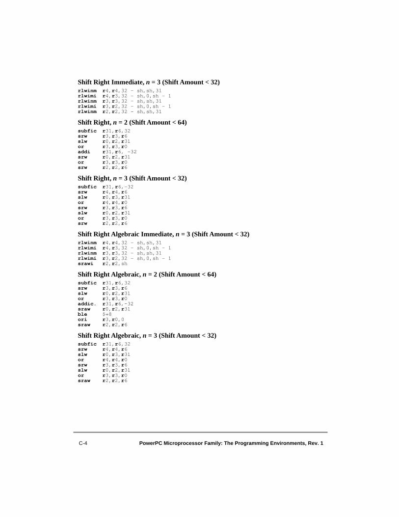
C-4 PowerPC Microprocessor Family: The Programming Environments, Rev. 1
Shift Right Immediate, n = 3 (Shift Amount < 32)rlwinm r4,r4,32 – sh,sh,31rlwimi r4,r3,32 – sh,0,sh – 1rlwinm r3,r3,32 – sh,sh,31rlwimi r3,r2,32 – sh,0,sh – 1rlwinm r2,r2,32 – sh,sh,31
Shift Right, n = 2 (Shift Amount < 64)subfic r31,r6,32srw r3,r3,r6slw r0,r2,r31or r3,r3,r0addi r31,r6, –32srw r0,r2,r31or r3,r3,r0srw r2,r2,r6
Shift Right, n = 3 (Shift Amount < 32)subfic r31,r6,–32srw r4,r4,r6slw r0,r3,r31or r4,r4,r0srw r3,r3,r6slw r0,r2,r31or r3,r3,r0srw r2,r2,r6
Shift Right Algebraic Immediate, n = 3 (Shift Amount < 32) rlwinm r4,r4,32 – sh,sh,31rlwimi r4,r3,32 – sh,0,sh – 1rlwinm r3,r3,32 – sh,sh,31rlwimi r3,r2,32 – sh,0,sh – 1srawi r2,r2,sh
Shift Right Algebraic, n = 2 (Shift Amount < 64)subfic r31,r6,32srw r3,r3,r6slw r0,r2,r31or r3,r3,r0addic. r31,r6,–32sraw r0,r2,r31ble $+8ori r3,r0,0sraw r2,r2,r6
Shift Right Algebraic, n = 3 (Shift Amount < 32)subfic r31,r6,32srw r4,r4,r6slw r0,r3,r31or r4,r4,r0srw r3,r3,r6slw r0,r2,r31or r3,r3,r0sraw r2,r2,r6

Appendix D. Floating-Point Models D-1
Appendix DFloating-Point ModelsD0D0
This appendix describes the execution model for IEEE operations and gives examples ofhow the floating-point conversion instructions can be used to perform various conversionsas well as providing models for floating-point instructions.
D.1 Execution Model for IEEE OperationsThe following description uses double-precision arithmetic as an example; single-precisionarithmetic is similar except that the fraction field is a 23-bit field and the single-precisionguard, round, and sticky bits (described in this section) are logically adjacent to the 23-bitFRACTION field.
IEEE-conforming significand arithmetic is performed with a floating-point accumulatorwhere bits 0–55, shown in Figure D-1, comprise the significand of the intermediate result.
Figure D-1. IEEE 64-Bit Execution Model
The bits and fields for the IEEE double-precision execution model are defined as follows:
• The S bit is the sign bit.
• The C bit is the carry bit that captures the carry out of the significand.
• The L bit is the leading unit bit of the significand that receives the implicit bit from the operands.
• The FRACTION is a 52-bit field that accepts the fraction of the operands.
• The guard (G), round (R), and sticky (X) bits are extensions to the low-order bits of the accumulator. The G and R bits are required for postnormalization of the result. The G, R, and X bits are required during rounding to determine if the intermediate result is equally near the two nearest representable values. The X bit serves as an extension to the G and R bits by representing the logical OR of all bits that may
0 1 52 55
S C L FRACTION XG R

D-2 PowerPC Microprocessor Family: The Programming Environments, Rev. 1
appear to the low-order side of the R bit, due to either shifting the accumulator right or to other generation of low-order result bits. The G and R bits participate in the left shifts with zeros being shifted into the R bit.
Table D-1 shows the significance of the G, R, and X bits with respect to the intermediateresult (IR), the next lower in magnitude representable number (NL), and the next higher inmagnitude representable number (NH).
The significand of the intermediate result is made up of the L bit, the FRACTION, and theG, R, and X bits.
The infinitely precise intermediate result of an operation is the result normalized in bits L,FRACTION, G, R, and X of the floating-point accumulator.
After normalization, the intermediate result is rounded, using the rounding mode specifiedby FPSCR[RN]. If rounding causes a carry into C, the significand is shifted right oneposition and the exponent is incremented by one. This causes an inexact result and possiblyexponent overflow. Fraction bits to the left of the bit position used for rounding are storedinto the FPR, and low-order bit positions, if any, are set to zero.
Four user-selectable rounding modes are provided through FPSCR[RN] as described inSection 3.3.5, “Rounding.” For rounding, the conceptual guard, round, and sticky bits aredefined in terms of accumulator bits.
Table D-2 shows the positions of the guard, round, and sticky bits for double-precision andsingle-precision floating-point numbers in the IEEE execution model.
Table D-1. Interpretation of G, R, and X Bits
G R X Interpretation
0 0 0 IR is exact
0 0 1
0 1 0 IR closer to NL
0 1 1
1 0 0 IR midway between NL & NH
1 0 1
1 1 0 IR closer to NH
1 1 1

Appendix D. Floating-Point Models D-3
Rounding can be treated as though the significand were shifted right, if required, until theleast-significant bit to be retained is in the low-order bit position of the FRACTION. If anyof the guard, round, or sticky bits are nonzero, the result is inexact.
Z1 and Z2, defined in Section 3.3.5, “Rounding,” can be used to approximate the result inthe target format when one of the following rules is used:
• Round to nearest
— Guard bit = 0: The result is truncated. (Result exact (GRX = 000) or closest to next lower value in magnitude (GRX = 001, 010, or 011).
— Guard bit = 1: Depends on round and sticky bits:
Case a: If the round or sticky bit is one (inclusive), the result is incremented (result closest to next higher value in magnitude (GRX = 101, 110, or 111)).
Case b: If the round and sticky bits are zero (result midway between closest representable values) then if the low-order bit of the result is one, the result is incremented. Otherwise (the low-order bit of the result is zero) the result is truncated (this is the case of a tie rounded to even).
If during the round-to-nearest process, truncation of the unrounded number produces the maximum magnitude for the specified precision, the following action is taken:
— Guard bit = 1: Store infinity with the sign of the unrounded result.
— Guard bit = 0: Store the truncated (maximum magnitude) value.
• Round toward zero—Choose the smaller in magnitude of Z1 or Z2. If the guard, round, or sticky bit is nonzero, the result is inexact.
• Round toward +infinity—Choose Z1.
• Round toward –infinity—Choose Z2.
Where the result is to have fewer than 53 bits of precision because the instruction is afloating round to single-precision or single-precision arithmetic instruction, theintermediate result either is normalized or is placed in correct denormalized form beforebeing rounded.
Table D-2. Location of the Guard, Round, and Sticky Bits—IEEE Execution Model
Format Guard Round Sticky
Double G bit R bit X bit
Single 24 25 OR of 26–52 G,R,X
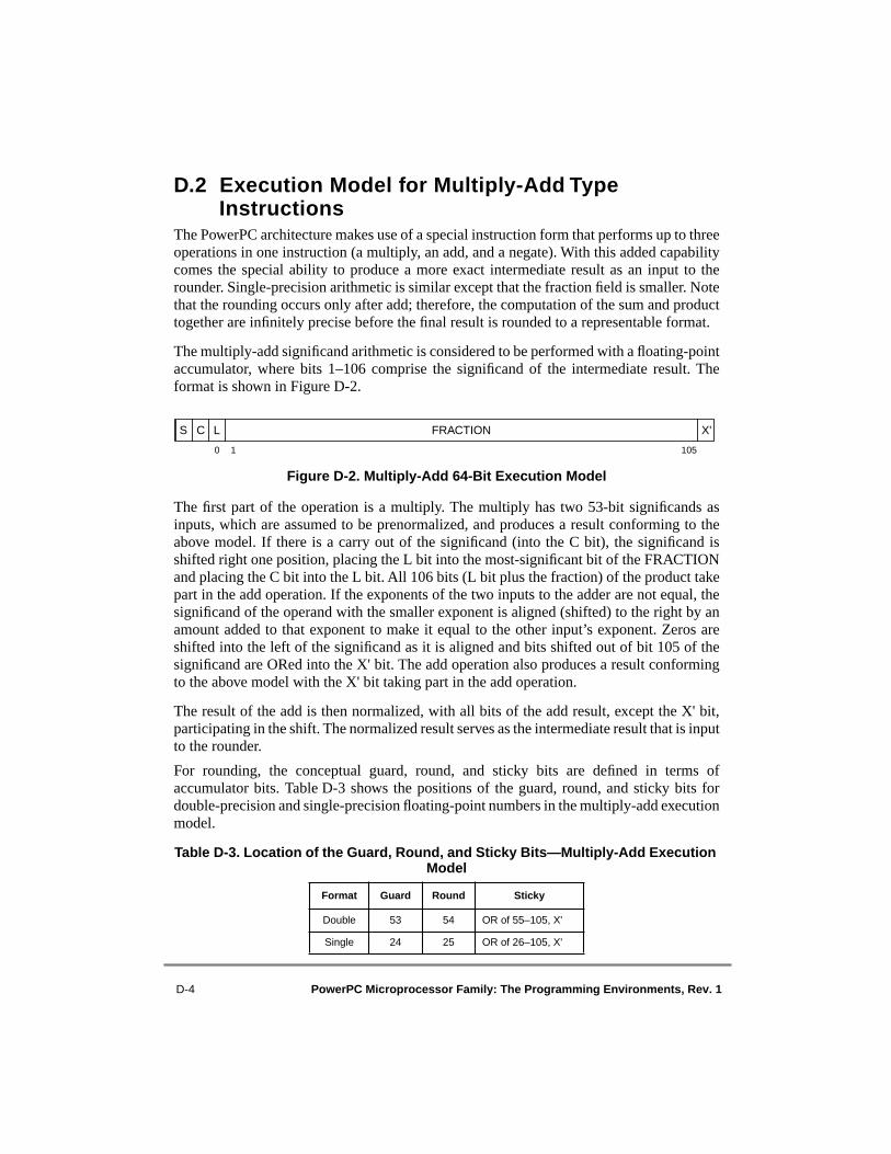
D-4 PowerPC Microprocessor Family: The Programming Environments, Rev. 1
D.2 Execution Model for Multiply-Add Type Instructions
The PowerPC architecture makes use of a special instruction form that performs up to threeoperations in one instruction (a multiply, an add, and a negate). With this added capabilitycomes the special ability to produce a more exact intermediate result as an input to therounder. Single-precision arithmetic is similar except that the fraction field is smaller. Notethat the rounding occurs only after add; therefore, the computation of the sum and producttogether are infinitely precise before the final result is rounded to a representable format.
The multiply-add significand arithmetic is considered to be performed with a floating-pointaccumulator, where bits 1–106 comprise the significand of the intermediate result. Theformat is shown in Figure D-2.
Figure D-2. Multiply-Add 64-Bit Execution Model
The first part of the operation is a multiply. The multiply has two 53-bit significands asinputs, which are assumed to be prenormalized, and produces a result conforming to theabove model. If there is a carry out of the significand (into the C bit), the significand isshifted right one position, placing the L bit into the most-significant bit of the FRACTIONand placing the C bit into the L bit. All 106 bits (L bit plus the fraction) of the product takepart in the add operation. If the exponents of the two inputs to the adder are not equal, thesignificand of the operand with the smaller exponent is aligned (shifted) to the right by anamount added to that exponent to make it equal to the other input’s exponent. Zeros areshifted into the left of the significand as it is aligned and bits shifted out of bit 105 of thesignificand are ORed into the X' bit. The add operation also produces a result conformingto the above model with the X' bit taking part in the add operation.
The result of the add is then normalized, with all bits of the add result, except the X' bit,participating in the shift. The normalized result serves as the intermediate result that is inputto the rounder.
For rounding, the conceptual guard, round, and sticky bits are defined in terms ofaccumulator bits. Table D-3 shows the positions of the guard, round, and sticky bits fordouble-precision and single-precision floating-point numbers in the multiply-add executionmodel.
Table D-3. Location of the Guard, Round, and Sticky Bits—Multiply-Add Execution Model
Format Guard Round Sticky
Double 53 54 OR of 55–105, X'
Single 24 25 OR of 26–105, X'
0 1 105
S C L FRACTION X'

Appendix D. Floating-Point Models D-5
The rules for rounding the intermediate result are the same as those given in Section D.1,“Execution Model for IEEE Operations.”
If the instruction is floating negative multiply-add or floating negative multiply-subtract,the final result is negated.
Floating-point multiply-add instructions combine a multiply and an add operation withoutan intermediate rounding operation. The fraction part of the intermediate product is 106 bitswide, and all 106 bits take part in the add/subtract portion of the instruction.
Status bits are set as follows:
• Overflow, underflow, and inexact exception bits, the FR and FI bits, and the FPRF field are set based on the final result of the operation, and not on the result of the multiplication.
• Invalid operation exception bits are set as if the multiplication and the addition were performed using two separate instructions (for example, an fmul instruction followed by an fadd instruction). That is, multiplication of infinity by 0 or of anything by an SNaN, causes the corresponding exception bits to be set.
D.3 Floating-Point ConversionsThis section provides examples of floating-point conversion instructions. Note that some ofthe examples use the optional Floating Select (fsel) instruction. Care must be taken in usingfsel if IEEE compatibility is required, or if the values being tested can be NaNs or infinities.
D.3.1 Conversion from Floating-Point Number to Floating-Point Integer
In a 64-bit implementation, the full convert to floating-point integer function can beimplemented with the following sequence assuming the floating-point value to beconverted is in FPR1, and the result is returned in FPR3.
mtfsb0 23 #clear VXCVIfctid[z]f3,f1 #convert to fx intfcfid f3,f3 #convert back againmcrfs 7,5 #VXCVI to CRbf 31,$+8 #skip if VXCVI was 0fmr f3,f1 #input was fp int

D-6 PowerPC Microprocessor Family: The Programming Environments, Rev. 1
D.3.2 Conversion from Floating-Point Number to Signed Fixed-Point Integer Double Word
This example applies to 64-bit implementations only.
The full convert to signed fixed-point integer double word function can be implementedwith the following sequence, assuming the floating-point value to be converted is in FPR1,the result is returned in GPR3, and a double word at displacement (disp) from the addressin GPR1 can be used as scratch space.
fctid[z]f2,f1 #convert to dword intstfd f2,disp(r1) #store floatld r3,disp(r1) #load dword
D.3.3 Conversion from Floating-Point Number to Unsigned Fixed-Point Integer Double Word
This example applies to 64-bit implementations only.
The full convert to unsigned fixed-point integer double word function can be implementedwith the following sequence, assuming the floating-point value to be converted is in FPR1,the value zero is in FPR0, the value 264 – 2048 is in FPR3, the value 263 is in FPR4 andGPR4, the result is returned in GPR3, and a double word at displacement (disp) from theaddress in GPR1 can be used as scratch space.
fsel f2,f1,f1,f0 #use 0 if < 0fsub f5,f3,f1 #use max if > maxfsel f2,f5,f2,f3fsub f5,f2,f4 #subtract 2**63fcmpu cr2,f2,f4 #use diff if ≥ 2**63fsel f2,f5,f5,f2fctid[z]f2,f2 #convert to fx intstfd f2,disp(r1) #store floatld r3,disp(r1) #load dwordblt cr2,$+8 #add 2**63 if inputadd r3,r3,r4 #was ≥ 2**63
D.3.4 Conversion from Floating-Point Number to Signed Fixed-Point Integer Word
The full convert to signed fixed-point integer word function can be implemented with thefollowing sequence, assuming that the floating-point value to be converted is in FPR1, theresult is returned in GPR3, and a double word at displacement (disp) from the address inGPR1 can be used as scratch space.
fctiw[z]f2,f1 #convert to fx intstfd f2,disp(r1) #store floatlwa r3,disp + 4(r1) #load word algebraic
#(use lwz on a 32-bit implementation)

Appendix D. Floating-Point Models D-7
D.3.5 Conversion from Floating-Point Number to Unsigned Fixed-Point Integer Word
In a 64-bit implementation, the full convert to unsigned fixed-point integer word functioncan be implemented with the following sequence, assuming the floating-point value to beconverted is in FPR1, the value zero is in FPR0, the value 232 – 1 is in FPR3, the result isreturned in GPR3, and a double word at displacement (disp) from the address in GPR1 canbe used as scratch space.
fsel f2,f1,f1,f0 #use 0 if < 0fsub f4,f3,f1 #use max if > maxfsel f2,f4,f2,f3fctid[z]f2,f2 #convert to fx intstfd f2,disp(r1) #store floatlwz r3,disp + 4(r1) #load word and zero
In a 32-bit implementation, the full convert to unsigned fixed-point integer word functioncan be implemented with the sequence shown below, assuming that the floating-point valueto be converted is in FPR1, the value zero is in FPR0, the value 232 – 1 is in FPR3, the value231 is in FPR4, the result is returned in GPR3, and a double word at displacement (disp)from the address in GPR1 can be used as scratch space.
fsel f2,f1,f1,f0 #use 0 if < 0fsub f5,f3,f1 #use max if > maxfsel f2,f5,f2,f3fsub f5,f2,f4 #subtract 2**31fcmpu cr2,f2,f4 #use diff if ≥ 2**31fsel f2,f5,f5,f2fctiw[z]f2,f2 #convert to fx intstfd f2,disp(r1) #store floatlwz r3,disp + 4(r1) #load wordblt cr2,$+8 #add 2**31 if inputxoris r3,r3,0x8000 #was ≥ 2**31
D.3.6 Conversion from Signed Fixed-Point Integer Double Word to Floating-Point Number
This example applies to 64-bit implementations only.
The full convert from signed fixed-point integer double word function, using the roundingmode specified by FPSCR[RN], can be implemented with the following sequence,assuming the fixed-point value to be converted is in GPR3, the result is returned in FPR1,and a double word at displacement (disp) from the address in GPR1 can be used as scratchspace.
std r3,disp(r1) #store dwordlfd f1,disp(r1) #load floatfcfid f1,f1 #convert to fpu int

D-8 PowerPC Microprocessor Family: The Programming Environments, Rev. 1
D.3.7 Conversion from Unsigned Fixed-Point Integer Double Word to Floating-Point Number
This example applies to 64-bit implementations only.
The full convert from unsigned fixed point integer double word function, using therounding mode specified by FPSCR[RN], can be implemented with the followingsequence, assuming the fixed-point value to be converted is in GPR3, the value 232 is inFPR4, the result is returned in FPR1, and two double words at displacement (disp) from theaddress in GPR1 is used as scratch space.
rldicl r2,r3,32,32 #isolate high halfrldicl r0,r3,0,32 #isolate low halfstd r2,disp(r1) #store dword bothstd r0,disp + 8(r1)lfd f2,disp(r1) #load float bothlfd f1,disp + 8(r1) #load float bothfcfid f2,f2 #convert each half to fcfid f1,f1 #fpu int (no rnd)fmadd f1,f4,f2,f1 #(2**32)*high+low
(only add can rnd)
An alternative, shorter, sequence can be used if rounding according to FPSCR[RN] isdesired and FPSCR[RN] specifies round toward +infinity or round toward –infinity, or if itis acceptable for the rounded answer to be either of the two representable floating-pointintegers nearest to the given fixed-point integer. In this case the full convert from unsignedfixed-point integer double word function can be implemented with the following sequence,assuming the value 264 is in FPR2.
std r3,disp(r1) #store dwordlfd f1,disp(r1) #load floatfcfid f1,f1 #convert to fpu intfadd f4,f1,f2 #add 2**64fsel f1,f1,f1,f4 #if r3 < 0
D.3.8 Conversion from Signed Fixed-Point Integer Word to Floating-Point Number
In a 64-bit implementation, the full convert from signed fixed-point integer word functioncan be implemented with the following sequence, assuming the fixed-point value to beconverted is in GPR3, the result is returned in FPR1, and a double word at displacement(disp) from the address in GPR1 can be used as scratch space. (The result is exact.)
extsw r3,r3 #extend signstd r3,disp(r1) #store dwordlfd f1,disp(r1) #load floatfcfid f1,f1 #convert to fpu int
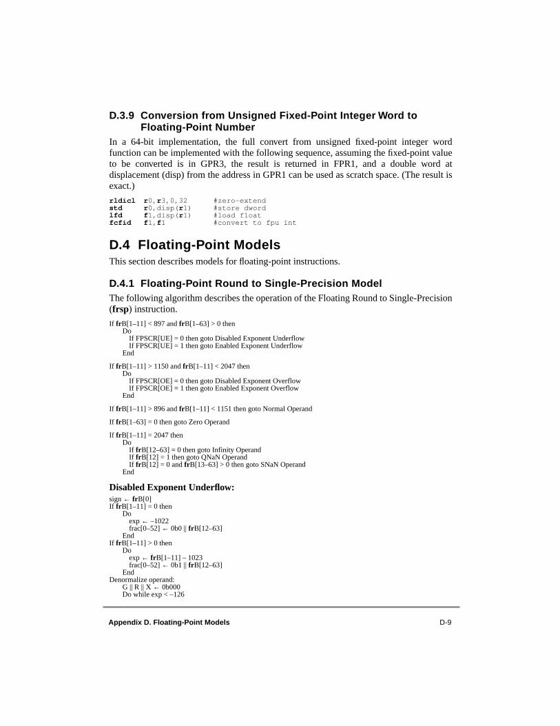
Appendix D. Floating-Point Models D-9
D.3.9 Conversion from Unsigned Fixed-Point Integer Word to Floating-Point Number
In a 64-bit implementation, the full convert from unsigned fixed-point integer wordfunction can be implemented with the following sequence, assuming the fixed-point valueto be converted is in GPR3, the result is returned in FPR1, and a double word atdisplacement (disp) from the address in GPR1 can be used as scratch space. (The result isexact.)
rldicl r0,r3,0,32 #zero-extendstd r0,disp(r1) #store dwordlfd f1,disp(r1) #load floatfcfid f1,f1 #convert to fpu int
D.4 Floating-Point ModelsThis section describes models for floating-point instructions.
D.4.1 Floating-Point Round to Single-Precision ModelThe following algorithm describes the operation of the Floating Round to Single-Precision(frsp) instruction.
If frB[1–11] < 897 and frB[1–63] > 0 thenDo
If FPSCR[UE] = 0 then goto Disabled Exponent UnderflowIf FPSCR[UE] = 1 then goto Enabled Exponent Underflow
End
If frB[1–11] > 1150 and frB[1–11] < 2047 thenDo
If FPSCR[OE] = 0 then goto Disabled Exponent Overflow If FPSCR[OE] = 1 then goto Enabled Exponent Overflow
End
If frB[1–11] > 896 and frB[1–11] < 1151 then goto Normal Operand
If frB[1–63] = 0 then goto Zero Operand
If frB[1–11] = 2047 thenDo
If frB[12–63] = 0 then goto Infinity OperandIf frB[12] = 1 then goto QNaN OperandIf frB[12] = 0 and frB[13–63] > 0 then goto SNaN Operand
End
Disabled Exponent Underflow:sign ← frB[0]If frB[1–11] = 0 then
Doexp ← –1022frac[0–52] ← 0b0 || frB[12–63]
EndIf frB[1–11] > 0 then
Doexp ← frB[1–11] – 1023frac[0–52] ← 0b1 || frB[12–63]
EndDenormalize operand:
G || R || X ← 0b000 Do while exp < –126

D-10 PowerPC Microprocessor Family: The Programming Environments, Rev. 1
exp ← exp + 1frac[0–52] || G || R || X ← 0b0 || frac || G || (R | X)
EndFPSCR[UX] ← frac[24–52] || G || R || X > 0Round single(sign,exp,frac[0–52],G,R,X)FPSCR[XX] ← FPSCR[XX] | FPSCR[FI]If frac[0–52] = 0 then
DofrD[0] ← signfrD[1–63] ← 0If sign = 0 then FPSCR[FPRF] ← “+zero” If sign = 1 then FPSCR[FPRF] ← “–zero”
EndIf frac[0–52] > 0 then
DoIf frac[0] = 1 then
DoIf sign = 0 then FPSCR[FPRF] ← “+normal number” If sign = 1 then FPSCR[FPRF] ← “–normal number”
EndIf frac[0] = 0 then
DoIf sign = 0 then FPSCR[FPRF] ← “+denormalized number” If sign = 1 then FPSCR[FPRF] ← “–denormalized number”
EndNormalize operand:
Do while frac[0] = 0exp ← exp – 1frac[0–52] ← frac[1–52] || 0b0
EndfrD[0] ← signfrD[1–11] ← exp + 1023frD[12–63] ← frac[1–52]
EndDone
Enabled Exponent UnderflowFPSCR[UX] ← 1sign ← frB[0]If frB[1–11] = 0 then
Doexp ← –1022frac[0–52] ← 0b0 || frB[12–63]
EndIf frB[1–11] > 0 then
Doexp ← frB[1–11] – 1023frac[0–52] ← 0b1 || frB[12–63]
End
Normalize operand:Do while frac[0] = 0
exp ← exp – 1frac[0–52] ← frac[1–52] || 0b0
EndRound single(sign,exp,frac[0–52],0,0,0)FPSCR[XX] ← FPSCR[XX] | FPSCR[FI]exp ← exp + 192frD[0] ← signfrD[1–11] ← exp + 1023frD[12–63] ← frac[1–52]If sign = 0 then FPSCR[FPRF] ← “+normal number” If sign = 1 then FPSCR[FPRF] ← “–normal number” Done

Appendix D. Floating-Point Models D-11
Disabled Exponent OverflowFPSCR[OX] ← 1If FPSCR[RN] = 0b00 then /* Round to Nearest */
DoIf frB[0] = 0 then frD ← 0x7FF0_0000_0000_0000 If frB[0] = 1 then frD ← 0xFFF0_0000_0000_0000 If frB[0] = 0 then FPSCR[FPRF] ← “+infinity”If frB[0] = 1 then FPSCR[FPRF] ← “–infinity”
EndIf FPSCR[RN] = 0b01 then /* Round Truncate */
DoIf frB[0] = 0 then frD ← 0x47EF_FFFF_E000_0000 If frB[0] = 1 then frD ← 0xC7EF_FFFF_E000_0000 If frB[0] = 0 then FPSCR[FPRF] ← “+normal number” If frB[0] = 1 then FPSCR[FPRF] ← “–normal number”
EndIf FPSCR[RN] = 0b10 then /* Round to +Infinity */
DoIf frB[0] = 0 then frD ← 0x7FF0_0000_0000_0000If frB[0] = 1 then frD ← 0xC7EF_FFFF_E000_0000If frB[0] = 0 then FPSCR[FPRF] ← “+infinity”If frB[0] = 1 then FPSCR[FPRF] ← “–normal number”
EndIf FPSCR[RN] = 0b11 then /* Round to -Infinity */
DoIf frB[0] = 0 then frD ← 0x47EF_FFFF_E000_0000If frB[0] = 1 then frD ← 0xFFF0_0000_0000_0000If frB[0] = 0 then FPSCR[FPRF] ← “+normal number” If frB[0] = 1 then FPSCR[FPRF] ← “–infinity”
EndFPSCR[FR] ← undefinedFPSCR[FI] ← 1FPSCR[XX] ← 1Done
Enabled Exponent Overflowsign ← frB[0]exp ← frB[1–11] – 1023
frac[0–52] ← 0b1 || frB[12–63]Round single(sign,exp,frac[0–52],0,0,0)FPSCR[XX] ← FPSCR[XX] | FPSCR[FI]
Enabled OverflowFPSCR[OX] ← 1exp ← exp – 192frD[0] ← signfrD[1–11] ← exp + 1023frD[12–63] ← frac[1–52]If sign = 0 then FPSCR[FPRF] ← “+normal number” If sign = 1 then FPSCR[FPRF] ← “–normal number”
Done
Zero OperandfrD ← frBIf frB[0] = 0 then FPSCR[FPRF] ← “+zero”If frB[0] = 1 then FPSCR[FPRF] ← “–zero”FPSCR[FR FI] ← 0b00Done
Infinity OperandfrD ← frBIf frB[0] = 0 then FPSCR[FPRF] ← “+infinity” If frB[0] = 1 then FPSCR[FPRF] ← “–infinity” Done

D-12 PowerPC Microprocessor Family: The Programming Environments, Rev. 1
QNaN Operand:frD ← frB[0–34] || 0b0_0000_0000_0000_0000_0000_0000_0000FPSCR[FPRF] ← “QNaN”FPSCR[FR FI] ← 0b00Done
SNaN OperandFPSCR[VXSNAN] ← 1If FPSCR[VE] = 0 then
DofrD[0–11] ← frB[0–11]frD[12] ← 1frD[13–63] ← frB[13–34] || 0b0_0000_0000_0000_0000_0000_0000_0000FPSCR[FPRF] ← “QNaN”
EndFPSCR[FR FI] ← 0b00Done
Normal Operandsign ← frB[0]exp ← frB[1–11] – 1023frac[0–52] ← 0b1 || frB[12–63]Round single(sign,exp,frac[0–52],0,0,0)FPSCR[XX] ← FPSCR[XX] | FPSCR[FI]If exp > +127 and FPSCR[OE] = 0 then go to Disabled Exponent OverflowIf exp > +127 and FPSCR[OE] = 1 then go to Enabled OverflowfrD[0] ← signfrD[1–11] ← exp + 1023frD[12–63] ← frac[1–52]If sign = 0 then FPSCR[FPRF] ← “+normal number” If sign = 1 then FPSCR[FPRF] ← “–normal number” Done
Round Single (sign,exp,frac[0–52],G,R,X)inc ← 0lsb ← frac[23]gbit ← frac[24]rbit ← frac[25]xbit ← (frac[26–52] || G || R || X) ≠ 0If FPSCR[RN] = 0b00 then
DoIf sign || lsb || gbit || rbit || xbit = 0bu11uu then inc ← 1If sign || lsb || gbit || rbit || xbit = 0bu011u then inc ← 1If sign || lsb || gbit || rbit || xbit = 0bu01u1 then inc ← 1
EndIf FPSCR[RN] = 0b10 then
DoIf sign || lsb || gbit || rbit || xbit = 0b0u1uu then inc ← 1If sign || lsb || gbit || rbit || xbit = 0b0uu1u then inc ← 1If sign || lsb || gbit || rbit || xbit = 0b0uuu1 then inc ← 1
EndIf FPSCR[RN] = 0b11 then
DoIf sign || lsb || gbit || rbit || xbit = 0b1u1uu then inc ← 1If sign || lsb || gbit || rbit || xbit = 0b1uu1u then inc ← 1If sign || lsb || gbit || rbit || xbit = 0b1uuu1 then inc ← 1
Endfrac[0–23] ← frac[0–23] + incIf carry_out =1 then
Dofrac[0–23] ← 0b1 || frac[0–22]exp ← exp + 1
End

Appendix D. Floating-Point Models D-13
frac[24–52] ← (29)0FPSCR[FR] ← incFPSCR[FI] ← gbit | rbit | xbitReturn
D.4.2 Floating-Point Convert to Integer ModelThe following algorithm describes the operation of the floating-point convert to integerinstructions. In this example, ‘u’ represents an undefined hexadecimal digit.
If Floating Convert to Integer WordThen Do
Then round_mode ← FPSCR[RN]tgt_precision ← “32-bit integer”
EndIf Floating Convert to Integer Word with round toward Zero
Then Doround_mode ← 0b01 tgt_precision ← “32-bit integer”
EndIf Floating Convert to Integer Double Word
Then Doround_mode ← FPSCR[RN]tgt_precision ← “64-bit integer”
EndIf Floating Convert to Integer Double Word with Round toward Zero
Then Doround_mode ← 0b01 tgt_precision ← “64-bit integer”
Endsign ← frB[0]If frB[1–11] = 2047 and frB[12–63] = 0 then goto Infinity OperandIf frB[1–11] = 2047 and frB[12] = 0 then goto SNaN OperandIf frB[1–11] = 2047 and frB[12] = 1 then goto QNaN OperandIf frB[1–11] > 1054 then goto Large Operand
If frB[1–11] > 0 then exp ← frB[1–11] – 1023 /* exp – bias */If frB[1–11] = 0 then exp ← –1022If frB[1–11] > 0 then frac[0–64]← 0b01 || frB[12–63] || (11)0 /*normal*/ If frB[1–11] = 0 then frac[0–64]← 0b00 || frB[12–63] || (11)0 /*denormal*/
gbit || rbit || xbit ← 0b000 Do i = 1,63 – exp /*do the loop 0 times if exp = 63*/
frac[0–64] || gbit || rbit || xbit ← 0b0 || frac[0–64] || gbit || (rbit | xbit)End
Round Integer (sign,frac[0–64],gbit,rbit,xbit,round_mode)In this example, ‘u’ represents an undefined hexadecimal digit. Comparisons ignore the ubits.
If sign = 1 then frac[0–64] ← ¬frac[0–64] + 1 /* needed leading 0 for –264 < frB < –263*/
If tgt_precision = “32-bit integer” and frac[0–64] > +231 – 1 then goto Large Operand
If tgt_precision = “64-bit integer” and frac[0–64] > +263 – 1 then goto Large Operand
If tgt_precision = “32-bit integer” and frac[0–64] < –231 then goto Large Operand
FPSCR[XX] ← FPSCR[XX] | FPSCR[FI]

D-14 PowerPC Microprocessor Family: The Programming Environments, Rev. 1
If tgt_precision = “64-bit integer” and frac[0–64] < –263 then goto Large OperandIf tgt_precision = “32-bit integer”
then frD ← 0xxuuu_uuuu || frac[33–64] If tgt_precision = “64-bit integer” then frD ← frac[1–64]FPSCR[FPRF] ← undefinedDone
Round Integer(sign,frac[0–64],gbit,rbit,xbit,round_mode)In this example, ‘u’ represents an undefined hexadecimal digit. Comparisons ignore the ubits.
inc ← 0If round_mode = 0b00 then
DoIf sign || frac[64] || gbit || rbit || xbit = 0bu11uu then inc ← 1 If sign || frac[64] || gbit || rbit || xbit = 0bu011u then inc ← 1 If sign || frac[64] || gbit || rbit || xbit = 0bu01u1 then inc ← 1
EndIf round_mode = 0b10 then
DoIf sign || frac[64] || gbit || rbit || xbit = 0b0u1uu then inc ←1If sign || frac[64] || gbit || rbit || xbit = 0b0uu1u then inc ← 1If sign || frac[64] || gbit || rbit || xbit = 0b0uuu1 then inc ← 1
EndIf round_mode = 0b11 then
DoIf sign || frac[64] || gbit || rbit || xbit = 0b1u1uu then inc ← 1If sign || frac[64] || gbit || rbit || xbit = 0b1uu1u then inc ← 1If sign || frac[64] || gbit || rbit || xbit = 0b1uuu1 then inc ← 1
Endfrac[0–64] ← frac[0–64] + incFPSCR[FR] ← incFPSCR[FI] ← gbit | rbit | xbitReturn
Infinity OperandFPSCR[FR FI VXCVI] ← 0b001If FPSCR[VE] = 0 then Do
If tgt_precision = “32-bit integer” thenDo
If sign = 0 then frD ← 0xuuuu_uuuu_7FFF_FFFF If sign = 1 then frD ← 0xuuuu_uuuu_8000_0000
EndElse
DoIf sign = 0 then frD ← 0x7FFF_FFFF_FFFF_FFFFIf sign = 1 then frD ← 0x8000_0000_0000_0000
EndFPSCR[FPRF] ← undefinedEnd
Done
SNaN OperandFPSCR[FR FI VXCVI VXSNAN] ← 0b0011 If FPSCR[VE] = 0 then
DoIf tgt_precision = “32-bit integer”
then frD ← 0xuuuu_uuuu_8000_0000If tgt_precision = “64-bit integer”
then frD ← 0x8000_0000_0000_0000FPSCR[FPRF] ← undefined
EndDone

Appendix D. Floating-Point Models D-15
QNaN OperandFPSCR[FR FI VXCVI] ← 0b001 If FPSCR[VE] = 0 then
DoIf tgt_precision = “32-bit integer” then frD ← 0xuuuu_uuuu_8000_0000If tgt_precision = “64-bit integer” then frD ← 0x8000_0000_0000_0000FPSCR[FPRF] ← undefined
EndDone
Large OperandFPSCR[FR FI VXCVI] ← 0b001 If FPSCR[VE] = 0 then Do
If tgt_precision = “32-bit integer” thenDo
If sign = 0 then frD ← 0xuuuu_uuuu_7FFF_FFFFIf sign = 1 then frD ← 0xuuuu_uuuu_8000_0000
EndElse
DoIf sign = 0 then frD ← 0x7FFF_FFFF_FFFF_FFFFIf sign = 1 then frD ← 0x8000_0000_0000_0000
EndFPSCR[FPRF] ← undefinedEnd
Done
D.4.3 Floating-Point Convert from Integer ModelThe following describes, algorithmically, the operation of the floating-point convert frominteger instructions.
sign ← frB[0]exp ← 63frac[0–63] ← frB
If frac[0–63] = 0 then go to Zero Operand
If sign = 1 then frac[0–63] ← ¬frac[0–63] + 1
Do while frac[0] = 0 frac[0–63] ← frac[1–63] || '0'exp ← exp – 1
End
Round Float(sign,exp,frac[0–63],FPSCR[RN])If sign = 1 then FPSCR[FPRF] ← “–normal number”If sign = 0 then FPSCR[FPRF] ← “+normal number”frD[0] ← signfrD[1–11] ← exp + 1023 frD[12–63] ← frac[1–52]Done
Zero OperandFPSCR[FR FI] ← 0b00FPSCR[FPRF] ← “+zero”frD ← 0x0000_0000_0000_0000Done

D-16 PowerPC Microprocessor Family: The Programming Environments, Rev. 1
Round Float(sign,exp,frac[0–63],round_mode)In this example ‘u’ represents an undefined hexadecimal digit. Comparisons ignore the ubits.
inc ← 0lsb ← frac[52]gbit ← frac[53]rbit ← frac[54]xbit ← frac[55–63] > 0If round_mode = 0b00 then
Do
If sign || lsb || gbit || rbit || xbit = 0bu11uu then inc ← 1If sign || lsb || gbit || rbit || xbit = 0bu011u then inc ← 1If sign || lsb || gbit || rbit || xbit = 0bu01u1 then inc ← 1
EndIf round_mode = 0b10 then
DoIf sign || lsb || gbit || rbit || xbit = 0b0u1uu then inc ← 1If sign || lsb || gbit || rbit || xbit = 0b0uu1u then inc ← 1If sign || lsb || gbit || rbit || xbit = 0b0uuu1 then inc ← 1
EndIf round_mode = 0b11 then
DoIf sign || lsb || gbit || rbit || xbit = 0b1u1uu then inc ← 1If sign || lsb || gbit || rbit || xbit = 0b1uu1u then inc ← 1If sign || lsb || gbit || rbit || xbit = 0b1uuu1 then inc ← 1
Endfrac[0–52] ← frac[0–52] + incIf carry_out = 1 then exp ← exp + 1FPSCR[FR] ← incFPSCR[FI] ← gbit | rbit | xbitFPSCR[XX] ← FPSCR[XX] | FPSCR[FI]Return
D.5 Floating-Point SelectionThe following are examples of how the optional fsel instruction can be used to implementfloating-point minimum and maximum functions, and certain simple forms of if-then-elseconstructions, without branching.
The examples show program fragments in an imaginary, C-like, high-level programminglanguage, and the corresponding program fragment using fsel and other PowerPCinstructions. In the examples, a, b, x, y, and z are floating-point variables, which areassumed to be in FPRs fa, fb, fx, fy, and fz. FPR fs is assumed to be available for scratchspace.
Additional examples can be found in Section D.3, “Floating-Point Conversions.”
Note that care must be taken in using fsel if IEEE compatibility is required, or if the valuesbeing tested can be NaNs or infinities; see Section D.5.4, “Notes.”

Appendix D. Floating-Point Models D-17
D.5.1 Comparison to ZeroThis section provides examples in a program fragment code sequence for the comparisonto zero case.
High-level language: PowerPC:if a ≥ 0.0 then x ← y fsel fx, fa, fy, fz (see Section D.5.4, “Notes” number 1)
else x ← z
if a > 0.0 then x ← y fneg fs, faelse x ← z fsel fx, fs, fz, fy (see Section D.5.4, “Notes” numbers 1 and 2)
if a = 0.0 then x ← y fsel fx, fa, fy, fzelse x ← z fneg fs, fa
fsel fx, fs, fx, fz (see Section D.5.4, “Notes” number 1)
D.5.2 Minimum and MaximumThis section provides examples in a program fragment code sequence for the minimum andmaximum cases.
High-level language: PowerPC:x ← min(a, b) fsub fs, fa, fb (see Section D.5.4, “Notes” numbers 3, 4, and 5)
fsel fx, fs, fb, fa
x ← max(a, b) fsub fs, fa, fb (see Section D.5.4, “Notes” numbers 3, 4, and 5)fsel fx, fs, fa, fb
D.5.3 Simple If-Then-Else ConstructionsThis section provides examples in a program fragment code sequence for simple if-then-else statements.
High-level language: PowerPC:if a ≥ b then x ← y fsub fs, fa, fb
else x ← z fsel fx, fs, fy, fz (see Section D.5.4, “Notes” numbers 4 and 5)
if a >b then x ← y fsub fs, fb, faelse x ← z fsel fx, fs, fz, fy (see Section D.5.4, “Notes” numbers 3, 4, and 5)
if a = b then x ← y fsub fs, fa, fbelse x ← z fsel fx, fs, fy, fz
fneg fs, fsfsel fx, fs, fx, fz (see Section D.5.4, “Notes” numbers 4 and 5)
D.5.4 NotesThe following notes apply to the examples found in Section D.5.1, “Comparison to Zero,”Section D.5.2, “Minimum and Maximum,” and Section D.5.3, “Simple If-Then-ElseConstructions,” and to the corresponding cases using the other three arithmetic relations (<,≤, and ≠). These notes should also be considered when any other use of fsel is contemplated.

D-18 PowerPC Microprocessor Family: The Programming Environments, Rev. 1
In these notes the “optimized program” is the PowerPC program shown, and the“unoptimized program” (not shown) is the corresponding PowerPC program that usesfcmpu and branch conditional instructions instead of fsel.
1. The unoptimized program affects the VXSNAN bit of the FPSCR, and therefore may cause the system error handler to be invoked if the corresponding exception is enabled, while the optimized program does not affect this bit. This property of the optimized program is incompatible with the IEEE standard. (Note that the architecture specification also refers to exceptions as interrupts.)
2. The optimized program gives the incorrect result if ‘a’ is a NaN.
3. The optimized program gives the incorrect result if ‘a’ and/or ‘b’ is a NaN (except that it may give the correct result in some cases for the minimum and maximum functions, depending on how those functions are defined to operate on NaNs).
4. The optimized program gives the incorrect result if ‘a’ and ‘b’ are infinities of the same sign. (Here it is assumed that invalid operation exceptions are disabled, in which case the result of the subtraction is a NaN. The analysis is more complicated if invalid operation exceptions are enabled, because in that case the target register of the subtraction is unchanged.)
5. The optimized program affects the OX, UX, XX, and VXISI bits of the FPSCR, and therefore may cause the system error handler to be invoked if the corresponding exceptions are enabled, while the unoptimized program does not affect these bits. This property of the optimized program is incompatible with the IEEE standard.
D.6 Floating-Point Load InstructionsThere are two basic forms of load instruction—single-precision and double-precision.Because the FPRs support only floating-point double format, single-precision load floating-point instructions convert single-precision data to double-precision format prior to loadingthe operands into the target FPR. The conversion and loading steps follow:
Let WORD[0–31] be the floating point single-precision operand accessed from memory.
Normalized OperandIf WORD[1–8] > 0 and WORD[1–8] < 255frD[0–1] ← WORD[0–1] frD[2] ← ¬ WORD[1] frD[3] ← ¬ WORD[1] frD[4] ← ¬ WORD[1] frD[5–63] ← WORD[2–31] || (29)0
Denormalized OperandIf WORD[1–8] = 0 and WORD[9–31] ≠ 0sign ← WORD[0] exp ← –126frac[0–52] ← 0b0 || WORD[9–31] || (29)0normalize the operandDo while frac[0] = 0
frac ← frac[1–52] || 0b0
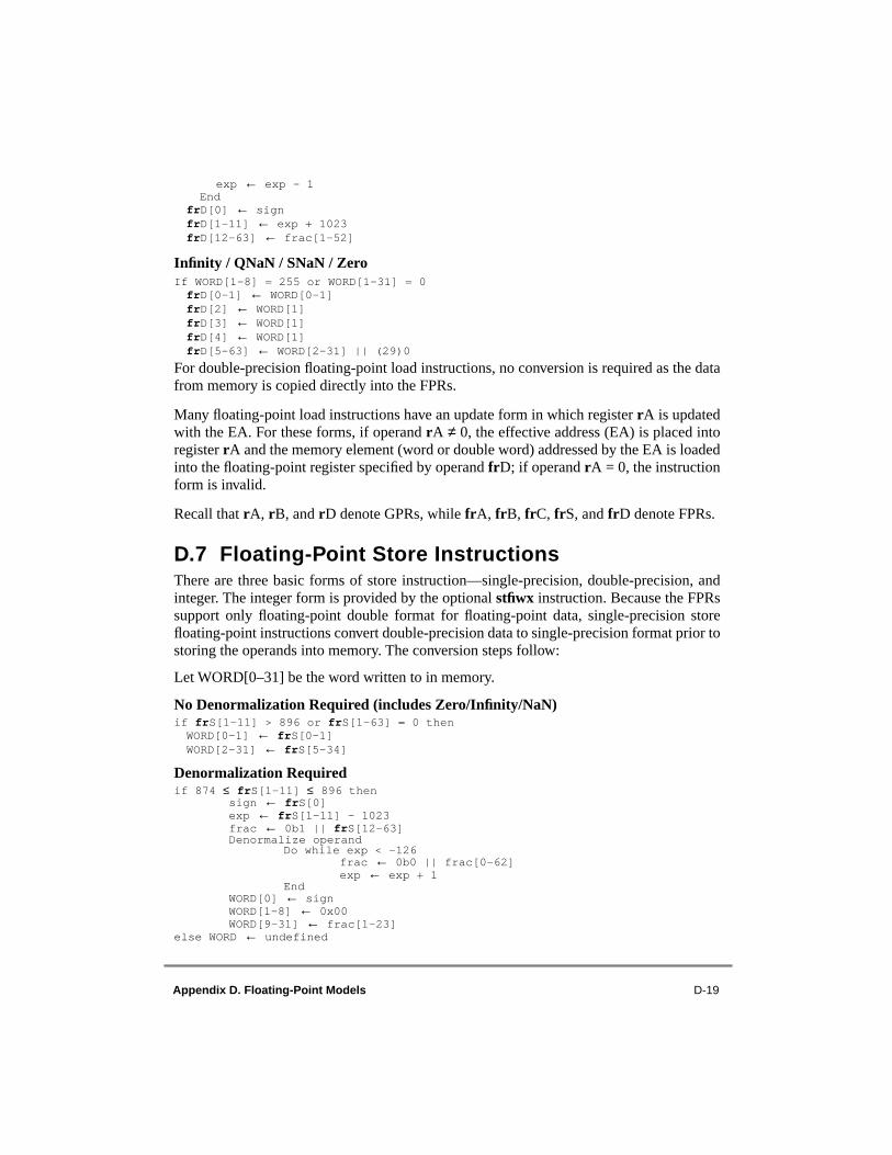
Appendix D. Floating-Point Models D-19
exp ← exp – 1End
frD[0] ← signfrD[1–11] ← exp + 1023frD[12–63] ← frac[1–52]
Infinity / QNaN / SNaN / ZeroIf WORD[1–8] = 255 or WORD[1–31] = 0frD[0–1] ← WORD[0–1] frD[2] ← WORD[1] frD[3] ← WORD[1] frD[4] ← WORD[1] frD[5–63] ← WORD[2–31] || (29)0
For double-precision floating-point load instructions, no conversion is required as the datafrom memory is copied directly into the FPRs.
Many floating-point load instructions have an update form in which register rA is updatedwith the EA. For these forms, if operand rA ≠ 0, the effective address (EA) is placed intoregister rA and the memory element (word or double word) addressed by the EA is loadedinto the floating-point register specified by operand frD; if operand rA = 0, the instructionform is invalid.
Recall that rA, rB, and rD denote GPRs, while frA, frB, frC, frS, and frD denote FPRs.
D.7 Floating-Point Store InstructionsThere are three basic forms of store instruction—single-precision, double-precision, andinteger. The integer form is provided by the optional stfiwx instruction. Because the FPRssupport only floating-point double format for floating-point data, single-precision storefloating-point instructions convert double-precision data to single-precision format prior tostoring the operands into memory. The conversion steps follow:
Let WORD[0–31] be the word written to in memory.
No Denormalization Required (includes Zero/Infinity/NaN)if frS[1–11] > 896 or frS[1–63] = 0 thenWORD[0–1] ← frS[0–1]WORD[2–31] ← frS[5–34]
Denormalization Requiredif 874 ≤ frS[1–11] ≤ 896 then
sign ← frS[0]exp ← frS[1–11] – 1023frac ← 0b1 || frS[12–63]Denormalize operand
Do while exp < –126frac ← 0b0 || frac[0–62]exp ← exp + 1
EndWORD[0] ← signWORD[1–8] ← 0x00WORD[9–31] ← frac[1–23]
else WORD ← undefined

D-20 PowerPC Microprocessor Family: The Programming Environments, Rev. 1
Notice that if the value to be stored by a single-precision store floating-point instruction islarger in magnitude than the maximum number representable in single format, the first casementioned, “No Denormalization Required,” applies. The result stored in WORD is then awell-defined value, but is not numerically equal to the value in the source register (that is,the result of a single-precision load floating-point from WORD will not compare equal tothe contents of the original source register).
Note that the description of conversion steps presented here is only a model. The actualimplementation may vary from this description but must produce results equivalent to whatthis model would produce.
It is important to note that for double-precision store floating-point instructions and for thestore floating-point as integer word instruction no conversion is required as the data fromthe FPR is copied directly into memory.

Appendix E. Synchronization Programming Examples E-1
Appendix ESynchronization Programming ExamplesE0E0
The examples in this appendix show how synchronization instructions can be used toemulate various synchronization primitives and how to provide more complex forms ofsynchronization.
For each of these examples, it is assumed that a similar sequence of instructions is used byall processes requiring synchronization of the accessed data.
E.1 General InformationThe following points provide general information about the lwarx and stwcx. instructions:
• In general, lwarx and stwcx. instructions should be paired, with the same effective address (EA) used for both. The only exception is that an unpaired stwcx. instruction to any (scratch) effective address can be used to clear any reservation held by the processor.
• It is acceptable to execute an lwarx instruction for which no stwcx. instruction is executed. Such a dangling lwarx instruction occurs in the example shown in Section E.2.5, “Test and Set,” if the value loaded is not zero.
• To increase the likelihood that forward progress is made, it is important that looping on lwarx/stwcx. pairs be minimized. For example, in the sequence shown in Section E.2.5, “Test and Set,” this is achieved by testing the old value before attempting the store—were the order reversed, more stwcx. instructions might be executed, and reservations might more often be lost between the lwarx and the stwcx. instructions.
• The manner in which lwarx and stwcx. are communicated to other processors and mechanisms, and between levels of the memory subsystem within a given processor, is implementation-dependent. In some implementations, performance may be improved by minimizing looping on an lwarx instruction that fails to return a desired value. For example, in the example provided in Section E.2.5, “Test and Set,” if the program stays in the loop until the word loaded is zero, the programmer can change the “bne- $+12” to “bne- loop.”

E-2 PowerPC Microprocessor Family: The Programming Environments, Rev. 1
In some implementations, better performance may be obtained by using an ordinary load instruction to do the initial checking of the value, as follows:
loop: lwz r5,0(r3) #load the wordcmpwi r5,0 #loop back if wordbne- loop #not equal to 0lwarx r5,0,r3 #try again, reservingcmpwi r5,0 #(likely to succeed)bne loop #try to store nonzerostwcx. r4,0,r3 #bne- loop #loop if lost reservation
• In a multiprocessor, livelock (a state in which processors interact in a way such that no processor makes progress) is possible if a loop containing an lwarx/stwcx. pair also contains an ordinary store instruction for which any byte of the affected memory area is in the reservation granule of the reservation. For example, the first code sequence shown in Section E.5, “List Insertion,” can cause livelock if two list elements have next element pointers in the same reservation granule.
Note that the examples in this appendix use the lwarx/stwcx. instructions, which addresswords in memory. For 64-bit implementations, these examples can be modified to addressdouble words by changing all lwarx instructions to ldarx instructions, all stwcx.instructions to stdcx. instructions, all stw instructions to std instructions, and all cmpw andcmpwi extended mnemonics to cmpd and cmpdi, respectively.
E.2 Synchronization PrimitivesThe following examples show how the lwarx and stwcx. instructions can be used toemulate various synchronization primitives. The sequences used to emulate the variousprimitives consist primarily of a loop using the lwarx and stwcx. instructions. Additionalsynchronization is unnecessary, because the stwcx. will fail, clearing the EQ bit, if the wordloaded by lwarx has changed before the stwcx. is executed.
E.2.1 Fetch and No-OpThe fetch and no-op primitive atomically loads the current value in a word in memory. Inthis example, it is assumed that the address of the word to be loaded is in GPR3 and the dataloaded are returned in GPR4.
loop: lwarx r4,0,r3 #load and reservestwcx. r4,0,r3 #store old value if still reservedbne- loop #loop if lost reservation
The stwcx., if it succeeds, stores to the destination location the same value that was loadedby the preceding lwarx. While the store is redundant with respect to the value in thelocation, its success ensures that the value loaded by the lwarx was the current value (thatis, the source of the value loaded by the lwarx was the last store to the location thatpreceded the stwcx. in the coherence order for the location).

Appendix E. Synchronization Programming Examples E-3
E.2.2 Fetch and StoreThe fetch and store primitive atomically loads and replaces a word in memory.
In this example, it is assumed that the address of the word to be loaded and replaced is inGPR3, the new value is in GPR4, and the old value is returned in GPR5.
loop: lwarx r5,0,r3 #load and reserve stwcx. r4,0,r3 #store new value if still reservedbne- loop #loop if lost reservation
E.2.3 Fetch and AddThe fetch and add primitive atomically increments a word in memory.
In this example, it is assumed that the address of the word to be incremented is in GPR3,the increment is in GPR4, and the old value is returned in GPR5.
loop: lwarx r5,0,r3 #load and reserveadd r0,r4,r5 #increment wordstwcx. r0,0,r3 #store new value if still reservedbne- loop #loop if lost reservation
E.2.4 Fetch and ANDThe fetch and AND primitive atomically ANDs a value into a word in memory.
In this example, it is assumed that the address of the word to be ANDed is in GPR3, thevalue to AND into it is in GPR4, and the old value is returned in GPR5.
loop: lwarx r5,0,r3 #load and reserveand r0,r4,r5 #AND wordstwcx. r0,0,r3 #store new value if still reservedbne- loop #loop if lost reservation
This sequence can be changed to perform another Boolean operation atomically on a word in memory, simply by changing the AND instruction to the desired Boolean instruction (OR, XOR, etc.).
E.2.5 Test and SetThis version of the test and set primitive atomically loads a word from memory, ensures thatthe word in memory is a nonzero value, and sets CR0[EQ] according to whether the valueloaded is zero.
In this example, it is assumed that the address of the word to be tested is in GPR3, the newvalue (nonzero) is in GPR4, and the old value is returned in GPR5.
loop: lwarx r5,0,r3 #load and reservecmpwi r5, 0 #done if wordbne $+12 #not equal to 0stwcx. r4,0,r3 #try to store non-zerobne- loop #loop if lost reservation
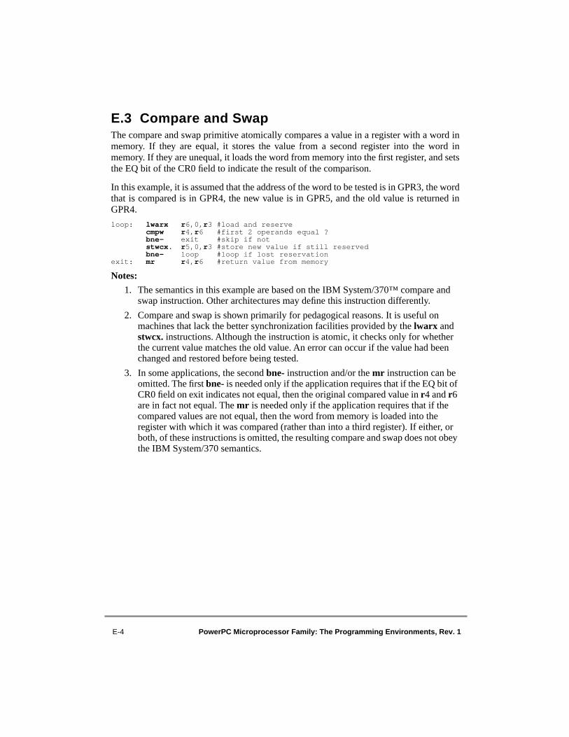
E-4 PowerPC Microprocessor Family: The Programming Environments, Rev. 1
E.3 Compare and SwapThe compare and swap primitive atomically compares a value in a register with a word inmemory. If they are equal, it stores the value from a second register into the word inmemory. If they are unequal, it loads the word from memory into the first register, and setsthe EQ bit of the CR0 field to indicate the result of the comparison.
In this example, it is assumed that the address of the word to be tested is in GPR3, the wordthat is compared is in GPR4, the new value is in GPR5, and the old value is returned inGPR4.
loop: lwarx r6,0,r3 #load and reservecmpw r4,r6 #first 2 operands equal ?bne- exit #skip if notstwcx. r5,0,r3 #store new value if still reservedbne- loop #loop if lost reservation
exit: mr r4,r6 #return value from memory
Notes:
1. The semantics in this example are based on the IBM System/370™ compare and swap instruction. Other architectures may define this instruction differently.
2. Compare and swap is shown primarily for pedagogical reasons. It is useful on machines that lack the better synchronization facilities provided by the lwarx and stwcx. instructions. Although the instruction is atomic, it checks only for whether the current value matches the old value. An error can occur if the value had been changed and restored before being tested.
3. In some applications, the second bne- instruction and/or the mr instruction can be omitted. The first bne- is needed only if the application requires that if the EQ bit of CR0 field on exit indicates not equal, then the original compared value in r4 and r6 are in fact not equal. The mr is needed only if the application requires that if the compared values are not equal, then the word from memory is loaded into the register with which it was compared (rather than into a third register). If either, or both, of these instructions is omitted, the resulting compare and swap does not obey the IBM System/370 semantics.
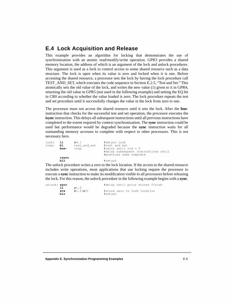
Appendix E. Synchronization Programming Examples E-5
E.4 Lock Acquisition and ReleaseThis example provides an algorithm for locking that demonstrates the use ofsynchronization with an atomic read/modify/write operation. GPR3 provides a sharedmemory location, the address of which is an argument of the lock and unlock procedures.This argument is used as a lock to control access to some shared resource such as a datastructure. The lock is open when its value is zero and locked when it is one. Beforeaccessing the shared resource, a processor sets the lock by having the lock procedure callTEST_AND_SET, which executes the code sequence in Section E.2.5, “Test and Set.” Thisatomically sets the old value of the lock, and writes the new value (1) given to it in GPR4,returning the old value in GPR5 (not used in the following example) and setting the EQ bitin CR0 according to whether the value loaded is zero. The lock procedure repeats the testand set procedure until it successfully changes the value in the lock from zero to one.
The processor must not access the shared resource until it sets the lock. After the bne-instruction that checks for the successful test and set operation, the processor executes theisync instruction. This delays all subsequent instructions until all previous instructions havecompleted to the extent required by context synchronization. The sync instruction could beused but performance would be degraded because the sync instruction waits for alloutstanding memory accesses to complete with respect to other processors. This is notnecessary here.
lock: li r4,1 #obtain lockloop: bl test_and_set #test and set
bne- loop #retry until old = 0#delay subsequent instructions until #previous ones complete
isyncblr #return
The unlock procedure writes a zero to the lock location. If the access to the shared resourceincludes write operations, most applications that use locking require the processor toexecute a sync instruction to make its modification visible to all processors before releasingthe lock. For this reason, the unlock procedure in the following example begins with a sync.
unlock: sync #delay until prior stores finishli r1,0stw r1,0(r3) #store zero to lock locationblr #return
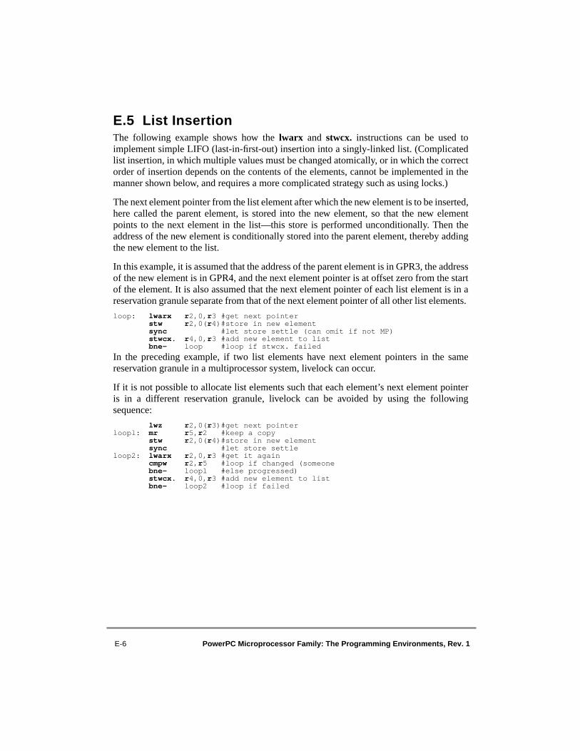
E-6 PowerPC Microprocessor Family: The Programming Environments, Rev. 1
E.5 List InsertionThe following example shows how the lwarx and stwcx. instructions can be used toimplement simple LIFO (last-in-first-out) insertion into a singly-linked list. (Complicatedlist insertion, in which multiple values must be changed atomically, or in which the correctorder of insertion depends on the contents of the elements, cannot be implemented in themanner shown below, and requires a more complicated strategy such as using locks.)
The next element pointer from the list element after which the new element is to be inserted,here called the parent element, is stored into the new element, so that the new elementpoints to the next element in the list—this store is performed unconditionally. Then theaddress of the new element is conditionally stored into the parent element, thereby addingthe new element to the list.
In this example, it is assumed that the address of the parent element is in GPR3, the addressof the new element is in GPR4, and the next element pointer is at offset zero from the startof the element. It is also assumed that the next element pointer of each list element is in areservation granule separate from that of the next element pointer of all other list elements.
loop: lwarx r2,0,r3 #get next pointerstw r2,0(r4)#store in new elementsync #let store settle (can omit if not MP)stwcx. r4,0,r3 #add new element to listbne- loop #loop if stwcx. failed
In the preceding example, if two list elements have next element pointers in the samereservation granule in a multiprocessor system, livelock can occur.
If it is not possible to allocate list elements such that each element’s next element pointeris in a different reservation granule, livelock can be avoided by using the followingsequence:
lwz r2,0(r3)#get next pointerloopl: mr r5,r2 #keep a copy
stw r2,0(r4)#store in new elementsync #let store settle
loop2: lwarx r2,0,r3 #get it againcmpw r2,r5 #loop if changed (someonebne- loopl #else progressed)stwcx. r4,0,r3 #add new element to listbne- loop2 #loop if failed
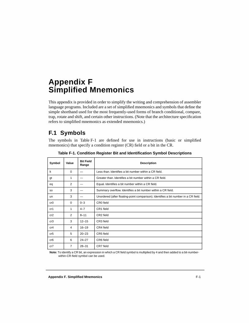
Appendix F. Simplified Mnemonics F-1
Appendix FSimplified MnemonicsF0F0
This appendix is provided in order to simplify the writing and comprehension of assemblerlanguage programs. Included are a set of simplified mnemonics and symbols that define thesimple shorthand used for the most frequently-used forms of branch conditional, compare,trap, rotate and shift, and certain other instructions. (Note that the architecture specificationrefers to simplified mnemonics as extended mnemonics.)
F.1 SymbolsThe symbols in Table F-1 are defined for use in instructions (basic or simplifiedmnemonics) that specify a condition register (CR) field or a bit in the CR.
Table F-1. Condition Register Bit and Identification Symbol Descriptions
Symbol ValueBit Field Range
Description
lt 0 — Less than. Identifies a bit number within a CR field.
gt 1 — Greater than. Identifies a bit number within a CR field.
eq 2 — Equal. Identifies a bit number within a CR field.
so 3 — Summary overflow. Identifies a bit number within a CR field.
un 3 — Unordered (after floating-point comparison). Identifies a bit number in a CR field.
cr0 0 0–3 CR0 field
cr1 1 4–7 CR1 field
cr2 2 8–11 CR2 field
cr3 3 12–15 CR3 field
cr4 4 16–19 CR4 field
cr5 5 20–23 CR5 field
cr6 6 24–27 CR6 field
cr7 7 28–31 CR7 field
Note: To identify a CR bit, an expression in which a CR field symbol is multiplied by 4 and then added to a bit-number-within-CR-field symbol can be used.

F-2 PowerPC Microprocessor Family: The Programming Environments, Rev. 1
Note that the simplified mnemonics in Section F.5.2, “Basic Branch Mnemonics,” andSection F.6, “Simplified Mnemonics for Condition Register Logical Instructions,” requireidentification of a CR bit—if one of the CR field symbols is used, it must be multiplied by4 and added to a bit-number-within-CR-field (value in the range of 0–3, explicit orsymbolic). The simplified mnemonics in Section F.5.3, “Branch Mnemonics IncorporatingConditions,” and Section F.3, “Simplified Mnemonics for Compare Instructions,” requireidentification of a CR field—if one of the CR field symbols is used, it must not be multipliedby 4. (For the simplified mnemonics in Section F.5.3, “Branch Mnemonics IncorporatingConditions,” the bit number within the CR field is part of the simplified mnemonic. The CRfield is identified, and the assembler does the multiplication and addition required toproduce a CR bit number for the BI field of the underlying basic mnemonic.)
F.2 Simplified Mnemonics for Subtract InstructionsThis section discusses simplified mnemonics for the subtract instructions.
F.2.1 Subtract ImmediateAlthough there is no subtract immediate instruction, its effect can be achieved by using anadd immediate instruction with the immediate operand negated. Simplified mnemonics areprovided that include this negation, making the intent of the computation more clear.
subi rD,rA,value (equivalent to addi rD,rA,–value)
subis rD,rA,value (equivalent to addis rD,rA,–value)
subic rD,rA,value (equivalent to addic rD,rA,–value)
subic. rD,rA,value (equivalent to addic. rD,rA,–value)
F.2.2 SubtractThe subtract from instructions subtract the second operand (rA) from the third (rB).Simplified mnemonics are provided that use the more normal order in which the thirdoperand is subtracted from the second. Both these mnemonics can be coded with an o suffixand/or dot (.) suffix to cause the OE and/or Rc bit to be set in the underlying instruction.
sub rD,rA,rB (equivalent to subf rD,rB,rA)
subc rD,rA,rB (equivalent to subfc rD,rB,rA)

Appendix F. Simplified Mnemonics F-3
F.3 Simplified Mnemonics for Compare InstructionsThe L field in the integer compare instructions controls whether the operands are treated as64-bit quantities (when L = 1) or as 32-bit quantities (when L = 0). Simplified mnemonicsare provided that represent the L value in the mnemonic rather than requiring it to be codedas a numeric operand.
The crfD field can be omitted if the result of the comparison is to be placed into the CR0field. Otherwise, the target CR field must be specified as the first operand. One of the CRfield symbols defined in Section F.1, “Symbols,” can be used for this operand.
Note that the basic compare mnemonics of PowerPC are the same as those of POWER, butthe POWER instructions have three operands while the PowerPC instructions have four.The assembler recognizes a basic compare mnemonic with the three operands as thePOWER form, and generates the instruction with L = 0. Although the crfD field cannormally be omitted when the CR0 field is the target, if L is specified the assembler requiresthat crfD be specified explicitly.
F.3.1 Double-Word ComparisonsThe instructions listed in Table F-2 are simplified mnemonics that should be supported byassemblers provided for 64-bit implementations.
Following are examples using the double-word compare mnemonics.
1. Compare rA and immediate value 100 as unsigned 64-bit integers and place result in CR0.cmpldi rA,100 (equivalent to cmpli 0,1,rA,100)
2. Same as (1), but place result in CR4.cmpldi cr4,rA,100 (equivalent to cmpli 4,1,rA,100)
3. Compare rA and rB as signed 64-bit integers and place result in CR0.cmpd rA,rB (equivalent to cmp 0,1,rA,rB)
F.3.2 Word ComparisonsThe instructions listed in Table F-3 are simplified mnemonics that should be supported byassemblers for all PowerPC implementations.
Table F-2. Simplified Mnemonics for Double-Word Compare Instructions
Operation Simplified Mnemonic Equivalent to:
Compare Double Word Immediate cmpdi crfD,rA,SIMM cmpi crfD,1,rA,SIMM
Compare Double Word cmpd crfD,rA,rB cmp crfD,1,rA,rB
Compare Logical Double Word Immediate cmpldi crfD,rA,UIMM cmpli crfD,1,rA,UIMM
Compare Logical Double Word cmpld crfD,rA,rB cmpl crfD,1,rA,rB

F-4 PowerPC Microprocessor Family: The Programming Environments, Rev. 1
Following are examples using the word compare mnemonics.
1. Compare rA[32–63] with immediate value 100 as signed 32-bit integers and place result in CR0.cmpwi rA,100 (equivalent to cmpi 0,0,rA,100)
2. Same as (1), but place results in CR4.cmpwi cr4,rA,100 (equivalent to cmpi 4,0,rA,100)
3. Compare rA[32–63] and rB[32–63] as unsigned 32-bit integers and place result in CR0.cmplw rA,rB (equivalent to cmpl 0,0,rA,rB)
F.4 Simplified Mnemonics for Rotate and Shift Instructions
The rotate and shift instructions provide powerful and general ways to manipulate registercontents, but can be difficult to understand. Simplified mnemonics that allow some of thesimpler operations to be coded easily are provided for the following types of operations:
• Extract—Select a field of n bits starting at bit position b in the source register; left or right justify this field in the target register; clear all other bits of the target register.
• Insert—Select a left-justified or right-justified field of n bits in the source register; insert this field starting at bit position b of the target register; leave other bits of the target register unchanged. (No simplified mnemonic is provided for insertion of a left-justified field, when operating on double words, because such an insertion requires more than one instruction.)
• Rotate—Rotate the contents of a register right or left n bits without masking.
• Shift—Shift the contents of a register right or left n bits, clearing vacated bits (logical shift).
• Clear—Clear the leftmost or rightmost n bits of a register.
• Clear left and shift left—Clear the leftmost b bits of a register, then shift the register left by n bits. This operation can be used to scale a (known non-negative) array index by the width of an element.
Table F-3. Simplified Mnemonics for Word Compare Instructions
Operation Simplified Mnemonic Equivalent to:
Compare Word Immediate cmpwi crfD,rA,SIMM cmpi crfD,0,rA,SIMM
Compare Word cmpw crfD,rA,rB cmp crfD,0,rA,rB
Compare Logical Word Immediate cmplwi crfD,rA,UIMM cmpli crfD,0,rA,UIMM
Compare Logical Word cmplw crfD,rA,rB cmpl crfD,0,rA,rB
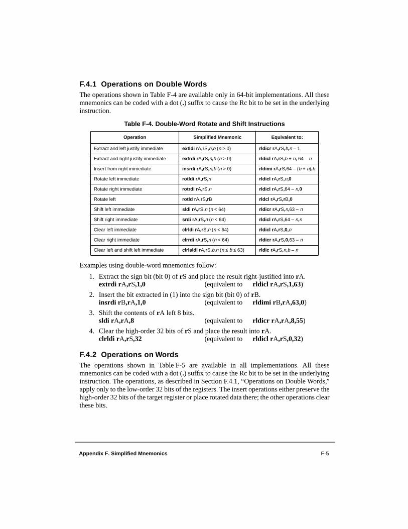
Appendix F. Simplified Mnemonics F-5
F.4.1 Operations on Double WordsThe operations shown in Table F-4 are available only in 64-bit implementations. All thesemnemonics can be coded with a dot (.) suffix to cause the Rc bit to be set in the underlyinginstruction.
Examples using double-word mnemonics follow:
1. Extract the sign bit (bit 0) of rS and place the result right-justified into rA.extrdi rA,rS,1,0 (equivalent to rldicl rA,rS,1,63)
2. Insert the bit extracted in (1) into the sign bit (bit 0) of rB.insrdi rB,rA,1,0 (equivalent to rldimi rB,rA,63,0)
3. Shift the contents of rA left 8 bits.sldi rA,rA,8 (equivalent to rldicr rA,rA,8,55)
4. Clear the high-order 32 bits of rS and place the result into rA.clrldi rA,rS,32 (equivalent to rldicl rA,rS,0,32)
F.4.2 Operations on WordsThe operations shown in Table F-5 are available in all implementations. All thesemnemonics can be coded with a dot (.) suffix to cause the Rc bit to be set in the underlyinginstruction. The operations, as described in Section F.4.1, “Operations on Double Words,”apply only to the low-order 32 bits of the registers. The insert operations either preserve thehigh-order 32 bits of the target register or place rotated data there; the other operations clearthese bits.
Table F-4. Double-Word Rotate and Shift Instructions
Operation Simplified Mnemonic Equivalent to:
Extract and left justify immediate extldi rA,rS,n,b (n > 0) rldicr rA,rS,b,n – 1
Extract and right justify immediate extrdi rA,rS,n,b (n > 0) rldicl rA,rS,b + n, 64 – n
Insert from right immediate insrdi rA,rS,n,b (n > 0) rldimi rA,rS,64 – (b + n),b
Rotate left immediate rotldi rA,rS,n rldicl rA,rS,n,0
Rotate right immediate rotrdi rA,rS,n rldicl rA,rS,64 – n,0
Rotate left rotld rA,rS,rB rldcl rA,rS,rB,0
Shift left immediate sldi rA,rS,n (n < 64) rldicr rA,rS,n,63 – n
Shift right immediate srdi rA,rS,n (n < 64) rldicl rA,rS,64 – n,n
Clear left immediate clrldi rA,rS,n (n < 64) rldicl rA,rS,0,n
Clear right immediate clrrdi rA,rS,n (n < 64) rldicr rA,rS,0,63 – n
Clear left and shift left immediate clrlsldi rA,rS,b,n (n ≤ b ≤ 63) rldic rA,rS,n,b – n
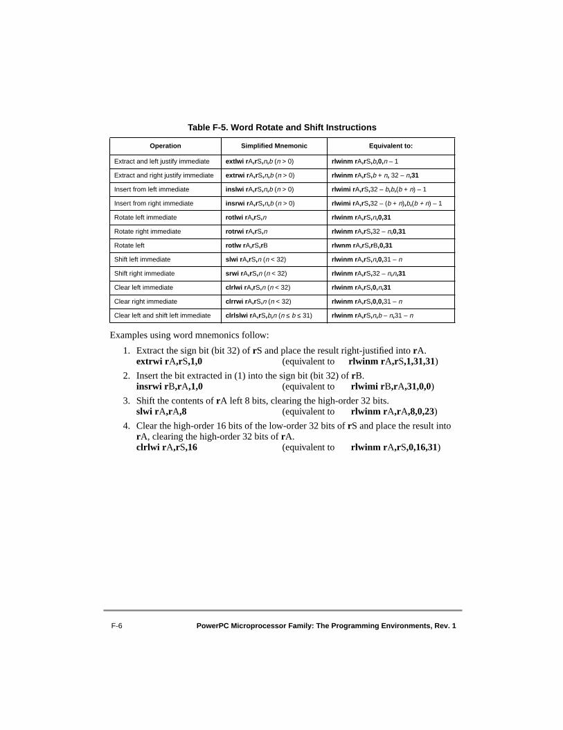
F-6 PowerPC Microprocessor Family: The Programming Environments, Rev. 1
Examples using word mnemonics follow:
1. Extract the sign bit (bit 32) of rS and place the result right-justified into rA.extrwi rA,rS,1,0 (equivalent to rlwinm rA,rS,1,31,31)
2. Insert the bit extracted in (1) into the sign bit (bit 32) of rB.insrwi rB,rA,1,0 (equivalent to rlwimi rB,rA,31,0,0)
3. Shift the contents of rA left 8 bits, clearing the high-order 32 bits.slwi rA,rA,8 (equivalent to rlwinm rA,rA,8,0,23)
4. Clear the high-order 16 bits of the low-order 32 bits of rS and place the result into rA, clearing the high-order 32 bits of rA.clrlwi rA,rS,16 (equivalent to rlwinm rA,rS,0,16,31)
Table F-5. Word Rotate and Shift Instructions
Operation Simplified Mnemonic Equivalent to:
Extract and left justify immediate extlwi rA,rS,n,b (n > 0) rlwinm rA,rS,b,0,n – 1
Extract and right justify immediate extrwi rA,rS,n,b (n > 0) rlwinm rA,rS,b + n, 32 – n,31
Insert from left immediate inslwi rA,rS,n,b (n > 0) rlwimi rA,rS,32 – b,b,(b + n) – 1
Insert from right immediate insrwi rA,rS,n,b (n > 0) rlwimi rA,rS,32 – (b + n),b,(b + n) – 1
Rotate left immediate rotlwi rA,rS,n rlwinm rA,rS,n,0,31
Rotate right immediate rotrwi rA,rS,n rlwinm rA,rS,32 – n,0,31
Rotate left rotlw rA,rS,rB rlwnm rA,rS,rB,0,31
Shift left immediate slwi rA,rS,n (n < 32) rlwinm rA,rS,n,0,31 – n
Shift right immediate srwi rA,rS,n (n < 32) rlwinm rA,rS,32 – n,n,31
Clear left immediate clrlwi rA,rS,n (n < 32) rlwinm rA,rS,0,n,31
Clear right immediate clrrwi rA,rS,n (n < 32) rlwinm rA,rS,0,0,31 – n
Clear left and shift left immediate clrlslwi rA,rS,b,n (n ≤ b ≤ 31) rlwinm rA,rS,n,b – n,31 – n

Appendix F. Simplified Mnemonics F-7
F.5 Simplified Mnemonics for Branch InstructionsMnemonics are provided so that branch conditional instructions can be coded with thecondition as part of the instruction mnemonic rather than as a numeric operand. Some ofthese are shown as examples with the branch instructions.
The mnemonics discussed in this section are variations of the branch conditionalinstructions.
F.5.1 BO and BI FieldsThe 5-bit BO field in branch conditional instructions encodes the following operations.
• Decrement count register (CTR)• Test CTR equal to zero• Test CTR not equal to zero• Test condition true• Test condition false• Branch prediction (taken, fall through)
The 5-bit BI field in branch conditional instructions specifies which of the 32 bits in the CRrepresents the condition to test.
To provide a simplified mnemonic for every possible combination of BO and BI fieldswould require 210 = 1024 mnemonics and most of these would be only marginally useful.The abbreviated set found in Section F.5.2, “Basic Branch Mnemonics,” is intended tocover the most useful cases. Unusual cases can be coded using a basic branch conditionalmnemonic (bc, bclr, bcctr) with the condition to be tested specified as a numeric operand.
F.5.2 Basic Branch MnemonicsThe mnemonics in Table F-6 allow all the common BO operand encodings to be specifiedas part of the mnemonic, along with the absolute address (AA), and set link register (LR)bits.
Notice that there are no simplified mnemonics for relative and absolute unconditionalbranches. For these, the basic mnemonics b, ba, bl, and bla are used.
Table F-6 provides the abbreviated set of simplified mnemonics for the most commonlyperformed conditional branches.

F-8 PowerPC Microprocessor Family: The Programming Environments, Rev. 1
The simplified mnemonics shown in Table F-6 that test a condition require a correspondingCR bit as the first operand of the instruction. The symbols defined in Section F.1,“Symbols,” can be used in the operand in place of a numeric value.
The simplified mnemonics found in Table F-6 are used in the following examples:
1. Decrement CTR and branch if it is still nonzero (closure of a loop controlled by a count loaded into CTR).bdnz target (equivalent to bc 16,0,target)
2. Same as (1) but branch only if CTR is non-zero and condition in CR0 is “equal.”bdnzt eq,target (equivalent to bc 8,2,target)
3. Same as (2), but “equal” condition is in CR5.bdnzt 4 * cr5 + eq,target (equivalent to bc 8,22,target)
4. Branch if bit 27 of CR is false.bf 27,target (equivalent to bc 4,27,target)
5. Same as (4), but set the link register. This is a form of conditional call.bfl 27,target (equivalent to bcl 4,27,target)
Table F-6. Simplified Branch Mnemonics
Branch Semantics
LR Update Not Enabled LR Update Enabled
bc Relative
bca Absolute
bclr to LR
bcctr to CTR
bcl Relative
bcla Absolute
bclrl to LR
bcctrl to CTR
Branch unconditionally — — blr bctr — — blrl bctrl
Branch if condition true bt bta btlr btctr btl btla btlrl btctrl
Branch if condition false
bf bfa bflr bfctr bfl bfla bflrl bfctrl
Decrement CTR, branch if CTR non-zero
bdnz bdnza bdnzlr — bdnzl bdnzla bdnzlrl —
Decrement CTR, branch if CTR non-zero AND condition true
bdnzt bdnzta bdnztlr — bdnztl bdnztla bdnztlrl —
Decrement CTR, branch if CTR non-zero AND condition false
bdnzf bdnzfa bdnzflr — bdnzfl bdnzfla bdnzflrl —
Decrement CTR, branch if CTR zero
bdz bdza bdzlr — bdzl bdzla bdzlrl —
Decrement CTR, branch if CTR zero AND condition true
bdzt bdzta bdztlr — bdztl bdztla bdztlrl —
Decrement CTR, branch if CTR zero AND condition false
bdzf bdzfa bdzflr — bdzfl bdzfla bdzflrl —
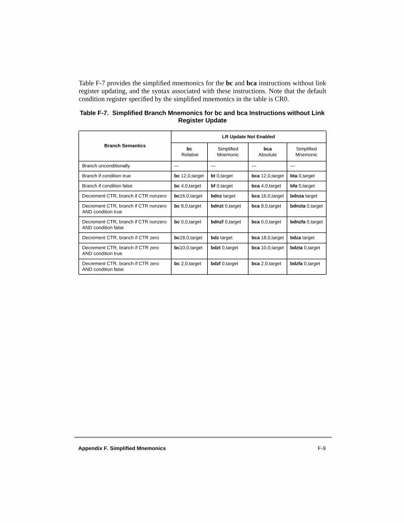
Appendix F. Simplified Mnemonics F-9
Table F-7 provides the simplified mnemonics for the bc and bca instructions without linkregister updating, and the syntax associated with these instructions. Note that the defaultcondition register specified by the simplified mnemonics in the table is CR0.
Table F-7. Simplified Branch Mnemonics for bc and bca Instructions without Link Register Update
Branch Semantics
LR Update Not Enabled
bc Relative
Simplified Mnemonic
bcaAbsolute
Simplified Mnemonic
Branch unconditionally — — — —
Branch if condition true bc 12,0,target bt 0,target bca 12,0,target bta 0,target
Branch if condition false bc 4,0,target bf 0,target bca 4,0,target bfa 0,target
Decrement CTR, branch if CTR nonzero bc16,0,target bdnz target bca 16,0,target bdnza target
Decrement CTR, branch if CTR nonzero AND condition true
bc 8,0,target bdnzt 0,target bca 8,0,target bdnzta 0,target
Decrement CTR, branch if CTR nonzero AND condition false
bc 0,0,target bdnzf 0,target bca 0,0,target bdnzfa 0,target
Decrement CTR, branch if CTR zero bc18,0,target bdz target bca 18,0,target bdza target
Decrement CTR, branch if CTR zero AND condition true
bc10,0,target
bdzt 0,target bca 10,0,target bdzta 0,target
Decrement CTR, branch if CTR zero AND condition false
bc 2,0,target bdzf 0,target bca 2,0,target bdzfa 0,target

F-10 PowerPC Microprocessor Family: The Programming Environments, Rev. 1
Table F-8 provides the simplified mnemonics for the bclr and bcclr instructions withoutlink register updating, and the syntax associated with these instructions. Note that thedefault condition register specified by the simplified mnemonics in the table is CR0.
Table F-8. Simplified Branch Mnemonics for bclr and bcclr Instructions without Link Register Update
Branch Semantics
LR Update Not Enabled
bclr to LR
Simplified Mnemonic
bcctr to CTRSimplified Mnemonic
Branch unconditionally bclr 20,0 blr bcctr 20,0 bctr
Branch if condition true bclr 12,0 btlr 0 bcctr 12,0 btctr 0
Branch if condition false bclr 4,0 bflr 0 bcctr 4,0 bfctr 0
Decrement CTR, branch if CTR nonzero
bclr 16,0 bdnzlr — —
Decrement CTR, branch if CTR nonzero AND condition true
bclr 10,0 bdztlr 0 — —
Decrement CTR, branch if CTR nonzero AND condition false
bclr 0,0 bdnzflr 0 — —
Decrement CTR, branch if CTR zero
bclr 18,0 bdzlr — —
Decrement CTR, branch if CTR zero AND condition true
bclr 10,0 bdztlr 0 — —
Decrement CTR, branch if CTR zero AND condition false
bcctr 0,0 bdzflr 0 — —
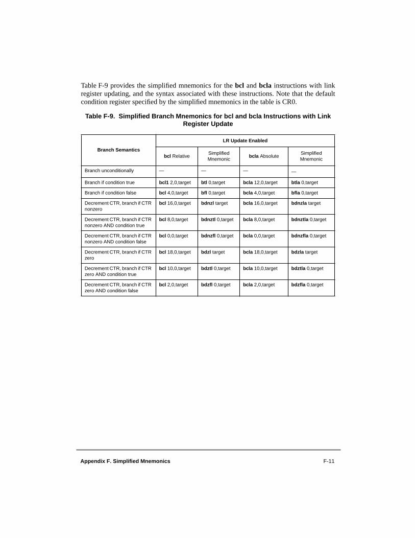
Appendix F. Simplified Mnemonics F-11
Table F-9 provides the simplified mnemonics for the bcl and bcla instructions with linkregister updating, and the syntax associated with these instructions. Note that the defaultcondition register specified by the simplified mnemonics in the table is CR0.
Table F-9. Simplified Branch Mnemonics for bcl and bcla Instructions with Link Register Update
Branch Semantics
LR Update Enabled
bcl RelativeSimplified Mnemonic
bcla AbsoluteSimplified Mnemonic
Branch unconditionally — — — —
Branch if condition true bcl1 2,0,target btl 0,target bcla 12,0,target btla 0,target
Branch if condition false bcl 4,0,target bfl 0,target bcla 4,0,target bfla 0,target
Decrement CTR, branch if CTR nonzero
bcl 16,0,target bdnzl target bcla 16,0,target bdnzla target
Decrement CTR, branch if CTR nonzero AND condition true
bcl 8,0,target bdnztl 0,target bcla 8,0,target bdnztla 0,target
Decrement CTR, branch if CTR nonzero AND condition false
bcl 0,0,target bdnzfl 0,target bcla 0,0,target bdnzfla 0,target
Decrement CTR, branch if CTR zero
bcl 18,0,target bdzl target bcla 18,0,target bdzla target
Decrement CTR, branch if CTR zero AND condition true
bcl 10,0,target bdztl 0,target bcla 10,0,target bdztla 0,target
Decrement CTR, branch if CTR zero AND condition false
bcl 2,0,target bdzfl 0,target bcla 2,0,target bdzfla 0,target

F-12 PowerPC Microprocessor Family: The Programming Environments, Rev. 1
Table F-10 provides the simplified mnemonics for the bclrl and bcctrl instructions withlink register updating, and the syntax associated with these instructions. Note that thedefault condition register specified by the simplified mnemonics in the table is CR0.
Table F-10. Simplified Branch Mnemonics for bclrl and bcctrl Instructions with Link Register Update
Branch Semantics
LR Update Enabled
bclrl to LR
Simplified Mnemonic
bcctrl to CTR
Simplified Mnemonic
Branch unconditionally bclrl 20,0 blrl bcctrl 20,0 bctrl
Branch if condition true bclrl12,0 btlrl 0 bcctrl 12,0 btctrl 0
Branch if condition false bclrl 4,0 bflrl 0 bcctrl 4,0 bfctrl 0
Decrement CTR, branch if CTR nonzero
bclrl 16,0 bdnzlrl — —
Decrement CTR, branch if CTR nonzero AND condition true
bclrl 8,0 bdnztlrl 0 — —
Decrement CTR, branch if CTR nonzero AND condition false
bclrl 0,0 bdnzflrl 0 — —
Decrement CTR, branch if CTR zero bclrl 18,0 bdzlrl — —
Decrement CTR, branch if CTR zero AND condition true
bdztlrl 0 bdztlrl 0 — —
Decrement CTR, branch if CTR zero AND condition false
bclrl 4,0 bflrl 0 — —

Appendix F. Simplified Mnemonics F-13
F.5.3 Branch Mnemonics Incorporating ConditionsThe mnemonics defined in Table F-6 are variations of the branch if condition true andbranch if condition false BO encodings, with the most useful values of BI represented inthe mnemonic rather than specified as a numeric operand.
A standard set of codes (shown in Table F-11) has been adopted for the most commoncombinations of branch conditions.
Table F-11. Standard Coding for Branch Conditions
Code Description
lt Less than
le Less than or equal
eq Equal
ge Greater than or equal
gt Greater than
nl Not less than
ne Not equal
ng Not greater than
so Summary overflow
ns Not summary overflow
un Unordered (after floating-point comparison)
nu Not unordered (after floating-point comparison)

F-14 PowerPC Microprocessor Family: The Programming Environments, Rev. 1
Table F-12 shows the simplified branch mnemonics incorporating conditions.
Instructions using the mnemonics in Table F-12 specify the condition register field in anoptional first operand. If the CR field being tested is CR0, this operand need not bespecified. One of the CR field symbols defined in Section F.1, “Symbols,” can be used forthis operand.
The simplified mnemonics found in Table F-12 are used in the following examples:
1. Branch if CR0 reflects condition “not equal.”bne target (equivalent to bc 4,2,target)
2. Same as (1) but condition is in CR3.bne cr3,target (equivalent to bc 4,14,target)
3. Branch to an absolute target if CR4 specifies “greater than,” setting the link register. This is a form of conditional “call.”bgtla cr4,target (equivalent to bcla 12,17,target)
4. Same as (3), but target address is in the CTR.bgtctrl cr4 (equivalent to bcctrl 12,17)
Table F-12. Simplified Branch Mnemonics with Comparison Conditions
Branch Semantics
LR Update Not Enabled LR Update Enabled
bc Relative
bca Absolute
bclr to LR
bcctr to CTR
bcl Relative
bcla Absolute
bclrl to LR
bcctrl to CTR
Branch if less than blt blta bltlr bltctr bltl bltla bltlrl bltctrl
Branch if less than or equal
ble blea blelr blectr blel blela blelrl blectrl
Branch if equal beq beqa beqlr beqctr beql beqla beqlrl beqctrl
Branch if greater than or equal
bge bgea bgelr bgectr bgel bgela bgelrl bgectrl
Branch if greater than bgt bgta bgtlr bgtctr bgtl bgtla bgtlrl bgtctrl
Branch if not less than bnl bnla bnllr bnlctr bnll bnlla bnllrl bnlctrl
Branch if not equal bne bnea bnelr bnectr bnel bnela bnelrl bnectrl
Branch if not greater than
bng bnga bnglr bngctr bngl bngla bnglrl bngctrl
Branch if summary overflow
bso bsoa bsolr bsoctr bsol bsola bsolrl bsoctrl
Branch if not summary overflow
bns bnsa bnslr bnsctr bnsl bnsla bnslrl bnsctrl
Branch if unordered bun buna bunlr bunctr bunl bunla bunlrl bunctrl
Branch if not unordered bnu bnua bnulr bnuctr bnul bnula bnulrl bnuctrl

Appendix F. Simplified Mnemonics F-15
Table F-13 shows the simplified branch mnemonics for the bc and bca instructions withoutlink register updating, and the syntax associated with these instructions. Note that thedefault condition register specified by the simplified mnemonics in the table is CR0.
Table F-13. Simplified Branch Mnemonics for bc and bca Instructions without Comparison Conditions and Link Register Updating
Branch Semantics
LR Update Not Enabled
bc RelativeSimplified Mnemonic
bca AbsoluteSimplified Mnemonic
Branch if less than bc 12,0,target blt target bca 12,0,target blta target
Branch if less than or equal bc 4,1,target ble target bca 4,1,target blea target
Branch if equal bc 12,2,target beq target bca 12,2,target beqa target
Branch if greater than or equal bc 4,0,target bge target bca 4,0,target bgea target
Branch if greater than bc 12,1,target bgt target bca 12,1,target bgta target
Branch if not less than bc 4,0,target bnl target bca 4,0,target bnla target
Branch if not equal bc 4,2,target bne target bca 4,2,target bnea target
Branch if not greater than bc 4,1,target bng target bca 4,1,target bnga target
Branch if summary overflow bc 12,3,target bso target bca 12,3,target bsoa target
Branch if not summary overflow bc 4,3,target bns target bca 4,3,target bnsa target
Branch if unordered bc 12,3,target bun target bca 12,3,target buna target
Branch if not unordered bc 4,3,target bnu target bca 4,3,target bnua target

F-16 PowerPC Microprocessor Family: The Programming Environments, Rev. 1
Table F-14 shows the simplified branch mnemonics for the bclr and bcctr instructionswithout link register updating, and the syntax associated with these instructions. Note thatthe default condition register specified by the simplified mnemonics in the table is CR0.
Table F-14. Simplified Branch Mnemonics for bclr and bcctr Instructions without Comparison Conditions and Link Register Updating
Branch Semantics
LR Update Not Enabled
bclr to LRSimplified Mnemonic
bcctr to CTRSimplified Mnemonic
Branch if less than bclr 12,0 bltlr bcctr 12,0 bltctr
Branch if less than or equal bclr 4,1 blelr bcctr 4,1 blectr
Branch if equal bclr 12,2 beqlr bcctr 12,2 beqctr
Branch if greater than or equal bclr 4,0 bgelr bcctr 4,0 bgectr
Branch if greater than bclr 12,1 bgtlr bcctr 12,1 bgtctr
Branch if not less than bclr 4,0 bnllr bcctr 4,0 bnlctr
Branch if not equal bclr 4,2 bnelr bcctr 4,2 bnectr
Branch if not greater than bclr 4,1 bnglr bcctr 4,1 bngctr
Branch if summary overflow bclr 12,3 bsolr bcctr 12,3 bsoctr
Branch if not summary overflow bclr 4,3 bnslr bcctr 4,3 bnsctr
Branch if unordered bclr 12,3 bunlr bcctr 12,3 bunctr
Branch if not unordered bclr 4,3 bnulr bcctr 4,3 bnuctr

Appendix F. Simplified Mnemonics F-17
Table F-15 shows the simplified branch mnemonics for the bcl and bcla instructions withlink register updating, and the syntax associated with these instructions. Note that thedefault condition register specified by the simplified mnemonics in the table is CR0.
Table F-15. Simplified Branch Mnemonics for bcl and bcla Instructions with Comparison Conditions and Link Register Update
Branch Semantics
LR Update Enabled
bcl RelativeSimplified Mnemonic
bcla AbsoluteSimplified Mnemonic
Branch if less than bcl 12,0,target bltl target bcla 12,0,target bltla target
Branch if less than or equal bcl 4,1,target blel target bcla 4,1,target blela target
Branch if equal beql target beql target bcla 12,2,target beqla target
Branch if greater than or equal bcl 4,0,target bgel target bcla 4,0,target bgela target
Branch if greater than bcl 12,1,target bgtl target bcla 12,1,target bgtla target
Branch if not less than bcl 4,0,target bnll target bcla 4,0,target bnlla target
Branch if not equal bcl 4,2,target bnel target bcla 4,2,target bnela target
Branch if not greater than bcl 4,1,target bngl target bcla 4,1,target bngla target
Branch if summary overflow bcl 12,3,target bsol target bcla 12,3,target bsola target
Branch if not summary overflow
bcl 4,3,target bnsl target bcla 4,3,target bnsla target
Branch if unordered bcl 12,3,target bunl target bcla 12,3,target bunla target
Branch if not unordered bcl 4,3,target bnul target bcla 4,3,target bnula target

F-18 PowerPC Microprocessor Family: The Programming Environments, Rev. 1
Table F-16 shows the simplified branch mnemonics for the bclrl and bcctl instructions withlink register updating, and the syntax associated with these instructions. Note that thedefault condition register specified by the simplified mnemonics in the table is CR0.
F.5.4 Branch PredictionIn branch conditional instructions that are not always taken, the low-order bit (y bit) of theBO field provides a hint about whether the branch is likely to be taken. See Section 4.2.4.2,“Conditional Branch Control,” for more information on the y bit.
Assemblers should clear this bit unless otherwise directed. This default action indicates thefollowing:
• A branch conditional with a negative displacement field is predicted to be taken.
• A branch conditional with a non-negative displacement field is predicted not to be taken (fall through).
• A branch conditional to an address in the LR or CTR is predicted not to be taken (fall through).
Table F-16. Simplified Branch Mnemonics for bclrl and bcctl Instructions with Comparison Conditions and Link Register Update
Branch Semantics
LR Update Enabled
bclrl to LRSimplified Mnemonic
bcctrl to CTRSimplified Mnemonic
Branch if less than bclrl 12,0 bltlrl 0 bcctrl 12,0 bltctrl 0
Branch if less than or equal bclrl 4,1 blelrl 0 bcctrl 4,1 blectrl 0
Branch if equal bclrl 12,2 beqlrl 0 bcctrl 12,2 beqctrl 0
Branch if greater than or equal bclrl 4,0 bgelrl 0 bcctrl 4,0 bgectrl 0
Branch if greater than bclrl 12,1 bgtlrl 0 bcctrl 12,1 bgtctrl 0
Branch if not less than bclrl 4,0 bnllrl 0 bcctrl 4,0 bnlctrl 0
Branch if not equal bclrl 4,2 bnelrl 0 bcctrl 4,2 bnectrl 0
Branch if not greater than bclrl 4,1 bnglrl 0 bcctrl 4,1 bngctrl 0
Branch if summary overflow bclrl 12,3 bsolrl 0 bcctrl 12,3 bsoctrl 0
Branch if not summary overflow bclrl 4,3 bnslrl 0 bcctrl 4,3 bnsctrl 0
Branch if unordered bclrl 12,3 bunlrl 0 bcctrl 12,3 bunctrl 0
Branch if not unordered bclrl 4,3 bnulrl 0 bcctrl 4,3 bnuctrl 0

Appendix F. Simplified Mnemonics F-19
If the likely outcome (branch or fall through) of a given branch conditional instruction isknown, a suffix can be added to the mnemonic that tells the assembler how to set the y bit.That is, ‘+’ indicates that the branch is to be taken and ‘–’ indicates that the branch is notto be taken. Such a suffix can be added to any branch conditional mnemonic, either basicor simplified.
For relative and absolute branches (bc[l][a]), the setting of the y bit depends on whether thedisplacement field is negative or non-negative. For negative displacement fields, coding thesuffix ‘+’ causes the bit to be cleared, and coding the suffix ‘–’ causes the bit to be set. Fornon-negative displacement fields, coding the suffix ‘+’ causes the bit to be set, and codingthe suffix ‘–’ causes the bit to be cleared.
For branches to an address in the LR or CTR (bcclr[l] or bcctr[l]), coding the suffix ‘+’causes the y bit to be set, and coding the suffix ‘–’ causes the bit to be cleared.
Examples of branch prediction follow:
1. Branch if CR0 reflects condition “less than,” specifying that the branch should be predicted to be taken.blt+ target
2. Same as (1), but target address is in the LR and the branch should be predicted not to be taken.bltlr–
F.6 Simplified Mnemonics for Condition Register Logical Instructions
The condition register logical instructions, shown in Table F-17, can be used to set, clear,copy, or invert a given condition register bit. Simplified mnemonics are provided that allowthese operations to be coded easily. Note that the symbols defined in Section F.1,“Symbols,” can be used to identify the condition register bit.
Table F-17. Condition Register Logical Mnemonics
Operation Simplified Mnemonic Equivalent to
Condition register set crset bx creqv bx,bx,bx
Condition register clear crclr bx crxor bx,bx,bx
Condition register move crmove bx,by cror bx,by,by
Condition register not crnot bx,by crnor bx,by,by

F-20 PowerPC Microprocessor Family: The Programming Environments, Rev. 1
Examples using the condition register logical mnemonics follow:
1. Set CR bit 25.crset 25 (equivalent to creqv 25,25,25)
2. Clear the SO bit of CR0.crclr so (equivalent to crxor 3,3,3)
3. Same as (2), but SO bit to be cleared is in CR3.crclr 4 * cr3 + so (equivalent to crxor 15,15,15)
4. Invert the EQ bit.crnot eq,eq (equivalent to crnor 2,2,2)
5. Same as (4), but EQ bit to be inverted is in CR4, and the result is to be placed into the EQ bit of CR5.crnot 4 * cr5 + eq, 4 * cr4 + eq (equivalent to crnor 22,18,18)
F.7 Simplified Mnemonics for Trap InstructionsA standard set of codes, shown in Table F-18, has been adopted for the most commoncombinations of trap conditions.
Table F-18. Standard Codes for Trap Instructions
Code Description TO Encoding < > = <U >U
lt Less than 16 1 0 0 0 0
le Less than or equal 20 1 0 1 0 0
eq Equal 4 0 0 1 0 0
ge Greater than or equal 12 0 1 1 0 0
gt Greater than 8 0 1 0 0 0
nl Not less than 12 0 1 1 0 0
ne Not equal 24 1 1 0 0 0
ng Not greater than 20 1 0 1 0 0
llt Logically less than 2 0 0 0 1 0
lle Logically less than or equal 6 0 0 1 1 0
lge Logically greater than or equal 5 0 0 1 0 1
lgt Logically greater than 1 0 0 0 0 1
lnl Logically not less than 5 0 0 1 0 1
lng Logically not greater than 6 0 0 1 1 0
— Unconditional 31 1 1 1 1 1
Note: The symbol “<U” indicates an unsigned less than evaluation will be performed. The symbol “>U” indi-cates an unsigned greater than evaluation will be performed.
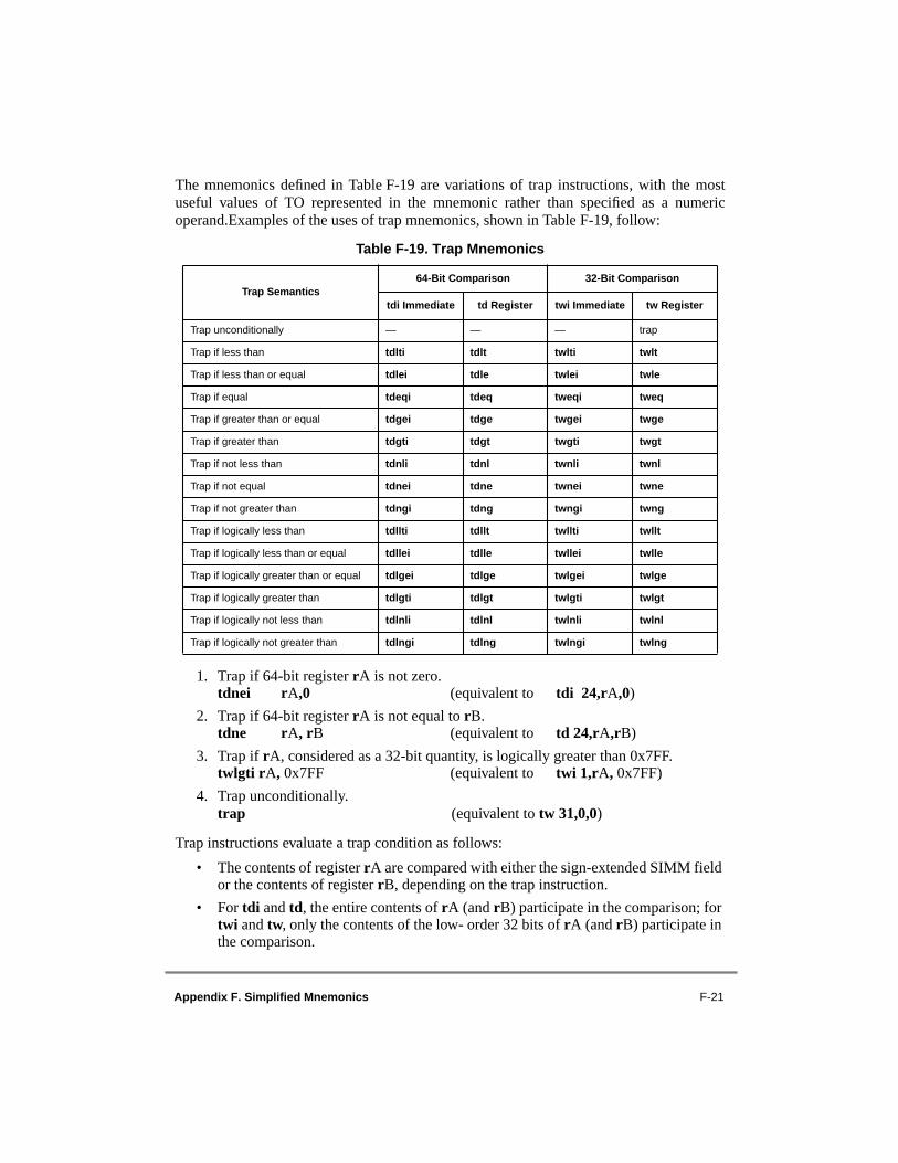
Appendix F. Simplified Mnemonics F-21
The mnemonics defined in Table F-19 are variations of trap instructions, with the mostuseful values of TO represented in the mnemonic rather than specified as a numericoperand.Examples of the uses of trap mnemonics, shown in Table F-19, follow:
1. Trap if 64-bit register rA is not zero.tdnei rA,0 (equivalent to tdi 24,rA,0)
2. Trap if 64-bit register rA is not equal to rB.tdne rA, rB (equivalent to td 24,rA,rB)
3. Trap if rA, considered as a 32-bit quantity, is logically greater than 0x7FF.twlgti rA, 0x7FF (equivalent to twi 1,rA, 0x7FF)
4. Trap unconditionally.trap (equivalent to tw 31,0,0)
Trap instructions evaluate a trap condition as follows:
• The contents of register rA are compared with either the sign-extended SIMM field or the contents of register rB, depending on the trap instruction.
• For tdi and td, the entire contents of rA (and rB) participate in the comparison; for twi and tw, only the contents of the low- order 32 bits of rA (and rB) participate in the comparison.
Table F-19. Trap Mnemonics
Trap Semantics64-Bit Comparison 32-Bit Comparison
tdi Immediate td Register twi Immediate tw Register
Trap unconditionally — — — trap
Trap if less than tdlti tdlt twlti twlt
Trap if less than or equal tdlei tdle twlei twle
Trap if equal tdeqi tdeq tweqi tweq
Trap if greater than or equal tdgei tdge twgei twge
Trap if greater than tdgti tdgt twgti twgt
Trap if not less than tdnli tdnl twnli twnl
Trap if not equal tdnei tdne twnei twne
Trap if not greater than tdngi tdng twngi twng
Trap if logically less than tdllti tdllt twllti twllt
Trap if logically less than or equal tdllei tdlle twllei twlle
Trap if logically greater than or equal tdlgei tdlge twlgei twlge
Trap if logically greater than tdlgti tdlgt twlgti twlgt
Trap if logically not less than tdlnli tdlnl twlnli twlnl
Trap if logically not greater than tdlngi tdlng twlngi twlng
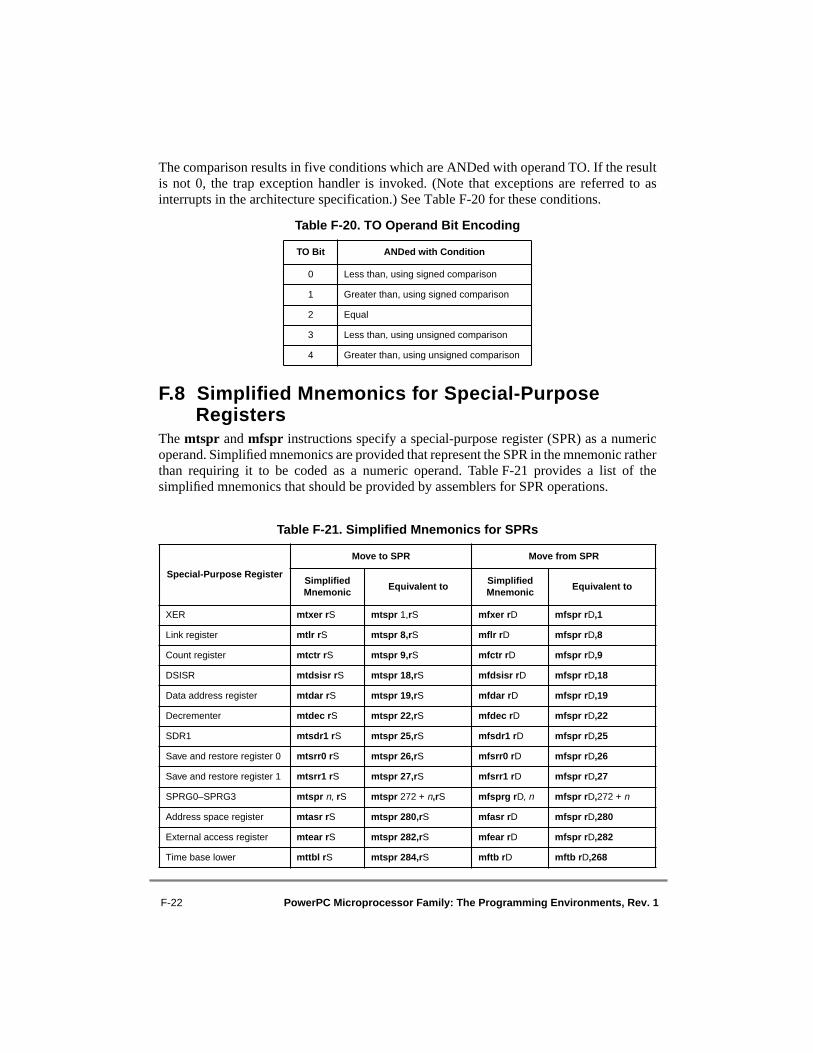
F-22 PowerPC Microprocessor Family: The Programming Environments, Rev. 1
The comparison results in five conditions which are ANDed with operand TO. If the resultis not 0, the trap exception handler is invoked. (Note that exceptions are referred to asinterrupts in the architecture specification.) See Table F-20 for these conditions.
F.8 Simplified Mnemonics for Special-Purpose Registers
The mtspr and mfspr instructions specify a special-purpose register (SPR) as a numericoperand. Simplified mnemonics are provided that represent the SPR in the mnemonic ratherthan requiring it to be coded as a numeric operand. Table F-21 provides a list of thesimplified mnemonics that should be provided by assemblers for SPR operations.
Table F-20. TO Operand Bit Encoding
TO Bit ANDed with Condition
0 Less than, using signed comparison
1 Greater than, using signed comparison
2 Equal
3 Less than, using unsigned comparison
4 Greater than, using unsigned comparison
Table F-21. Simplified Mnemonics for SPRs
Special-Purpose Register
Move to SPR Move from SPR
Simplified Mnemonic
Equivalent toSimplified Mnemonic
Equivalent to
XER mtxer rS mtspr 1,rS mfxer rD mfspr rD,1
Link register mtlr rS mtspr 8,rS mflr rD mfspr rD,8
Count register mtctr rS mtspr 9,rS mfctr rD mfspr rD,9
DSISR mtdsisr rS mtspr 18,rS mfdsisr rD mfspr rD,18
Data address register mtdar rS mtspr 19,rS mfdar rD mfspr rD,19
Decrementer mtdec rS mtspr 22,rS mfdec rD mfspr rD,22
SDR1 mtsdr1 rS mtspr 25,rS mfsdr1 rD mfspr rD,25
Save and restore register 0 mtsrr0 rS mtspr 26,rS mfsrr0 rD mfspr rD,26
Save and restore register 1 mtsrr1 rS mtspr 27,rS mfsrr1 rD mfspr rD,27
SPRG0–SPRG3 mtspr n, rS mtspr 272 + n,rS mfsprg rD, n mfspr rD,272 + n
Address space register mtasr rS mtspr 280,rS mfasr rD mfspr rD,280
External access register mtear rS mtspr 282,rS mfear rD mfspr rD,282
Time base lower mttbl rS mtspr 284,rS mftb rD mftb rD,268
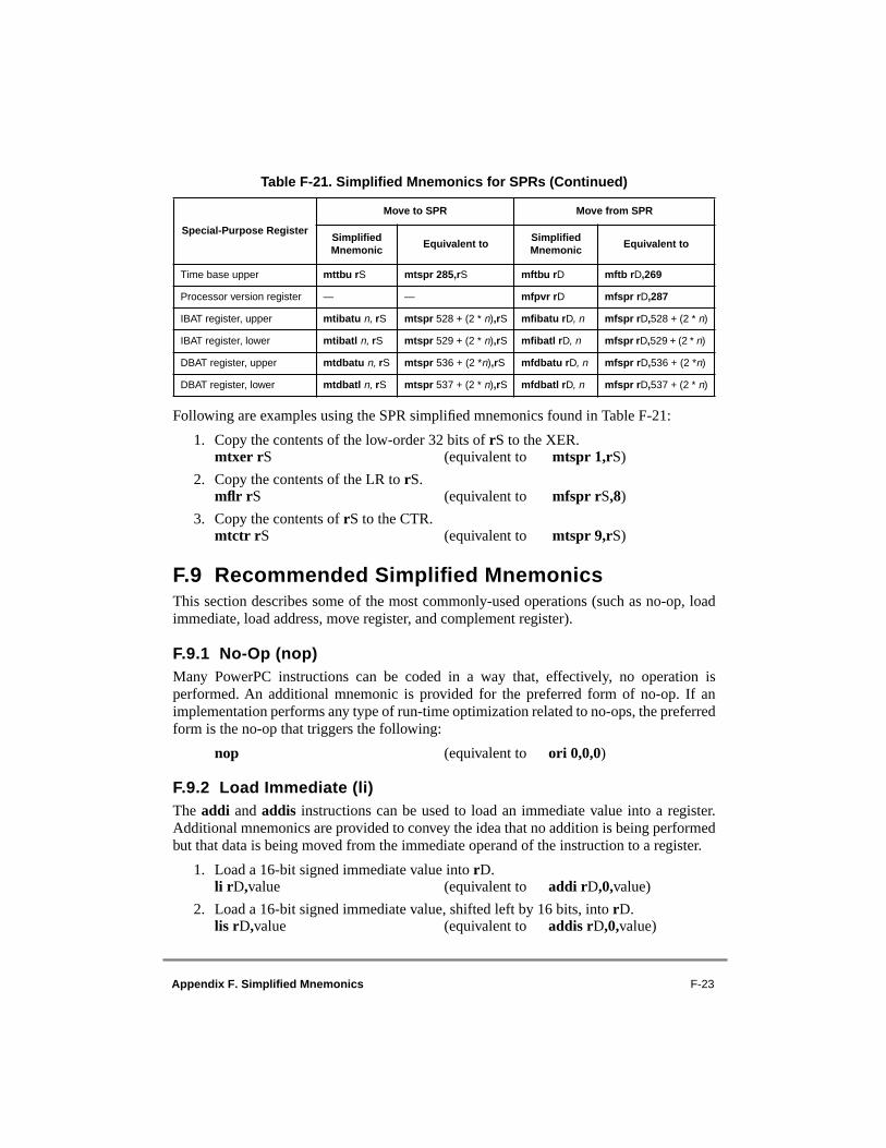
Appendix F. Simplified Mnemonics F-23
Following are examples using the SPR simplified mnemonics found in Table F-21:
1. Copy the contents of the low-order 32 bits of rS to the XER.mtxer rS (equivalent to mtspr 1,rS)
2. Copy the contents of the LR to rS.mflr rS (equivalent to mfspr rS,8)
3. Copy the contents of rS to the CTR.mtctr rS (equivalent to mtspr 9,rS)
F.9 Recommended Simplified MnemonicsThis section describes some of the most commonly-used operations (such as no-op, loadimmediate, load address, move register, and complement register).
F.9.1 No-Op (nop)Many PowerPC instructions can be coded in a way that, effectively, no operation isperformed. An additional mnemonic is provided for the preferred form of no-op. If animplementation performs any type of run-time optimization related to no-ops, the preferredform is the no-op that triggers the following:
nop (equivalent to ori 0,0,0)
F.9.2 Load Immediate (li)The addi and addis instructions can be used to load an immediate value into a register.Additional mnemonics are provided to convey the idea that no addition is being performedbut that data is being moved from the immediate operand of the instruction to a register.
1. Load a 16-bit signed immediate value into rD.li rD,value (equivalent to addi rD,0,value)
2. Load a 16-bit signed immediate value, shifted left by 16 bits, into rD. lis rD,value (equivalent to addis rD,0,value)
Time base upper mttbu rS mtspr 285,rS mftbu rD mftb rD,269
Processor version register — — mfpvr rD mfspr rD,287
IBAT register, upper mtibatu n, rS mtspr 528 + (2 * n),rS mfibatu rD, n mfspr rD,528 + (2 * n)
IBAT register, lower mtibatl n, rS mtspr 529 + (2 * n),rS mfibatl rD, n mfspr rD,529 + (2 * n)
DBAT register, upper mtdbatu n, rS mtspr 536 + (2 *n),rS mfdbatu rD, n mfspr rD,536 + (2 *n)
DBAT register, lower mtdbatl n, rS mtspr 537 + (2 * n),rS mfdbatl rD, n mfspr rD,537 + (2 * n)
Table F-21. Simplified Mnemonics for SPRs (Continued)
Special-Purpose Register
Move to SPR Move from SPR
Simplified Mnemonic
Equivalent toSimplified Mnemonic
Equivalent to

F-24 PowerPC Microprocessor Family: The Programming Environments, Rev. 1
F.9.3 Load Address (la)This mnemonic permits computing the value of a base-displacement operand, using theaddi instruction which normally requires a separate register and immediate operands.
la rD,d(rA) (equivalent to addi rD,rA,d)
The la mnemonic is useful for obtaining the address of a variable specified by name,allowing the assembler to supply the base register number and compute the displacement.If the variable v is located at offset dv bytes from the address in register rv, and theassembler has been told to use register rv as a base for references to the data structurecontaining v, the following line causes the address of v to be loaded into register rD:
la rD,v (equivalent to addi rD,rv,dv
F.9.4 Move Register (mr)Several PowerPC instructions can be coded to copy the contents of one register to another.A simplified mnemonic is provided that signifies that no computation is being performed,but merely that data is being moved from one register to another.
The following instruction copies the contents of rS into rA. This mnemonic can be codedwith a dot (.) suffix to cause the Rc bit to be set in the underlying instruction.
mr rA,rS (equivalent to or rA,rS,rS)
F.9.5 Complement Register (not)Several PowerPC instructions can be coded in a way that they complement the contents ofone register and place the result into another register. A simplified mnemonic is providedthat allows this operation to be coded easily.
The following instruction complements the contents of rS and places the result into rA.This mnemonic can be coded with a dot (.) suffix to cause the Rc bit to be set in theunderlying instruction.
not rA,rS (equivalent to nor rA,rS,rS)
F.9.6 Move to Condition Register (mtcr)This mnemonic permits copying the contents of the low-order 32 bits of a GPR to thecondition register, using the same syntax as the mfcr instruction.
mtcr rS (equivalent to mtcrf 0xFF,rS)

Glossary of Terms and Abbreviations Glossary-1
Glossary of Terms and AbbreviationsThe glossary contains an alphabetical list of terms, phrases, and abbreviations used in thisbook. Some of the terms and definitions included in the glossary are reprinted from IEEEStd. 754-1985, IEEE Standard for Binary Floating-Point Arithmetic, copyright ©1985 bythe Institute of Electrical and Electronics Engineers, Inc. with the permission of the IEEE.
Note that some terms are defined in the context of how they are used in this book.
Architecture. A detailed specification of requirements for a processor orcomputer system. It does not specify details of how the processor orcomputer system must be implemented; instead it provides atemplate for a family of compatible implementations.
Asynchronous exception. Exceptions that are caused by events external tothe processor’s execution. In this document, the term ‘asynchronousexception’ is used interchangeably with the word interrupt.
Atomic access. A bus access that attempts to be part of a read-write operationto the same address uninterrupted by any other access to that address(the term refers to the fact that the transactions are indivisible). ThePowerPC architecture implements atomic accesses through thelwarx/stwcx. (ldarx/stdcx. in 64-bit implementations) instructionpair.
BAT (block address translation) mechanism. A software-controlled arraythat stores the available block address translations on-chip.
Biased exponent. An exponent whose range of values is shifted by a constant(bias). Typically a bias is provided to allow a range of positive valuesto express a range that includes both positive and negative values.
Big-endian. A byte-ordering method in memory where the address n of aword corresponds to the most-significant byte. In an addressedmemory word, the bytes are ordered (left to right) 0, 1, 2, 3, with 0being the most-significant byte. See Little-endian.
A
B

Glossary-2 PowerPC Microprocessor Family: The Programming Environments, Rev. 1
Block. An area of memory that ranges from 128 Kbyte to 256 Mbyte, whosesize, translation, and protection attributes are controlled by the BATmechanism.
Boundedly undefined. A characteristic of results of certain operations thatare not rigidly prescribed by the PowerPC architecture. Boundedly-undefined results for a given operation may vary amongimplementations, and between execution attempts in the sameimplementation.
Although the architecture does not prescribe the exact behavior forwhen results are allowed to be boundedly undefined, the results ofexecuting instructions in contexts where results are allowed to beboundedly undefined are constrained to ones that could have beenachieved by executing an arbitrary sequence of defined instructions,in valid form, starting in the state the machine was in beforeattempting to execute the given instruction.
Cache. High-speed memory component containing recently-accessed dataand/or instructions (subset of main memory).
Cache block. A small region of contiguous memory that is copied frommemory into a cache. The size of a cache block may vary amongprocessors; the maximum block size is one page. In PowerPCprocessors, cache coherency is maintained on a cache-block basis.Note that the term ‘cache block’ is often used interchangeably with‘cache line’.
Cache coherency. An attribute wherein an accurate and common view ofmemory is provided to all devices that share the same memorysystem. Caches are coherent if a processor performing a read fromits cache is supplied with data corresponding to the most recent valuewritten to memory or to another processor’s cache.
Cache flush. An operation that removes from a cache any data from aspecified address range. This operation ensures that any modifieddata within the specified address range is written back to mainmemory. This operation is generated typically by a Data CacheBlock Flush (dcbf) instruction.
Caching-inhibited. A memory update policy in which the cache is bypassedand the load or store is performed to or from main memory.
Cast-outs. Cache blocks that must be written to memory when a cache misscauses a cache block to be replaced.
C

Glossary of Terms and Abbreviations Glossary-3
Changed bit. One of two page history bits found in each page table entry(PTE). The processor sets the changed bit if any store is performedinto the page. See also Page access history bits and Referenced bit.
Clear. To cause a bit or bit field to register a value of zero. See also Set.
Context synchronization. An operation that ensures that all instructions inexecution complete past the point where they can produce anexception, that all instructions in execution complete in the contextin which they began execution, and that all subsequent instructionsare fetched and executed in the new context. Context synchronizationmay result from executing specific instructions (such as isync or rfi)or when certain events occur (such as an exception).
Copy-back. An operation in which modified data in a cache block is copiedback to memory.
Denormalized number. A nonzero floating-point number whose exponenthas a reserved value, usually the format's minimum, and whoseexplicit or implicit leading significand bit is zero.
Direct-mapped cache. A cache in which each main memory address canappear in only one location within the cache, operates more quicklywhen the memory request is a cache hit.
Direct-store. Interface available on PowerPC processors only to supportdirect-store devices from the POWER architecture. When the T bitof a segment descriptor is set, the descriptor defines the region ofmemory that is to be used as a direct-store segment. Note that thisfacility is being phased out of the architecture and will not likely besupported in future devices. Therefore, software should not dependon it and new software should not use it.
Effective address (EA). The 32- or 64-bit address specified for a load, store,or an instruction fetch. This address is then submitted to the MMUfor translation to either a physical memory address or an I/O address.
Exception. A condition encountered by the processor that requires special,supervisor-level processing.
Exception handler. A software routine that executes when an exception istaken. Normally, the exception handler corrects the condition thatcaused the exception, or performs some other meaningful task (thatmay include aborting the program that caused the exception). Theaddress for each exception handler is identified by an exception
D
E

Glossary-4 PowerPC Microprocessor Family: The Programming Environments, Rev. 1
vector offset defined by the architecture and a prefix selected via theMSR.
Extended opcode. A secondary opcode field generally located in instructionbits 21–30, that further defines the instruction type. All PowerPCinstructions are one word in length. The most significant 6 bits of theinstruction are the primary opcode, identifying the type ofinstruction. See also Primary opcode.
Execution synchronization. A mechanism by which all instructions inexecution are architecturally complete before beginning execution(appearing to begin execution) of the next instruction. Similar tocontext synchronization but doesn't force the contents of theinstruction buffers to be deleted and refetched.
Exponent. In the binary representation of a floating-point number, theexponent is the component that normally signifies the integer powerto which the value two is raised in determining the value of therepresented number. See also Biased exponent.
Fetch. Retrieving instructions from either the cache or main memory andplacing them into the instruction queue.
Floating-point register (FPR). Any of the 32 registers in the floating-pointregister file. These registers provide the source operands anddestination results for floating-point instructions. Load instructionsmove data from memory to FPRs and store instructions move datafrom FPRs to memory. The FPRs are 64 bits wide and store floating-point values in double-precision format.
Fraction. In the binary representation of a floating-point number, the field ofthe significand that lies to the right of its implied binary point.
Fully-associative. Addressing scheme where every cache location (everybyte) can have any possible address.
General-purpose register (GPR). Any of the 32 registers in the general-purpose register file. These registers provide the source operands anddestination results for all integer data manipulation instructions.Integer load instructions move data from memory to GPRs and storeinstructions move data from GPRs to memory.
Guarded. The guarded attribute pertains to out-of-order execution. When apage is designated as guarded, instructions and data cannot beaccessed out-of-order.
F
G

Glossary of Terms and Abbreviations Glossary-5
Harvard architecture. An architectural model featuring separate caches forinstruction and data.
Hashing. An algorithm used in the page table search process.
IEEE 754. A standard written by the Institute of Electrical and ElectronicsEngineers that defines operations and representations of binaryfloating-point arithmetic.
Illegal instructions. A class of instructions that are not implemented for aparticular PowerPC processor. These include instructions not definedby the PowerPC architecture. In addition, for 32-bitimplementations, instructions that are defined only for 64-bitimplementations are considered to be illegal instructions. For 64-bitimplementations instructions that are defined only for 32-bitimplementations are considered to be illegal instructions.
Implementation. A particular processor that conforms to the PowerPCarchitecture, but may differ from other architecture-compliantimplementations for example in design, feature set, andimplementation of optional features. The PowerPC architecture hasmany different implementations.
Implementation-dependent. An aspect of a feature in a processor’s designthat is defined by a processor’s design specifications rather than bythe PowerPC architecture.
Implementation-specific. An aspect of a feature in a processor’s design thatis not required by the PowerPC architecture, but for which thePowerPC architecture may provide concessions to ensure thatprocessors that implement the feature do so consistently.
Imprecise exception. A type of synchronous exception that is allowed not toadhere to the precise exception model (see Precise exception). ThePowerPC architecture allows only floating-point exceptions to behandled imprecisely.
Inexact. Loss of accuracy in an arithmetic operation when the rounded resultdiffers from the infinitely precise value with unbounded range.
In-order. An aspect of an operation that adheres to a sequential model. Anoperation is said to be performed in-order if, at the time that it isperformed, it is known to be required by the sequential executionmodel. See Out-of-order.
H
HI

Glossary-6 PowerPC Microprocessor Family: The Programming Environments, Rev. 1
Instruction latency. The total number of clock cycles necessary to executean instruction and make ready the results of that instruction.
Instruction parallelism. A feature of PowerPC processors that allowsinstructions to be processed in parallel.
Interrupt. An asynchronous exception. On PowerPC processors, interruptsare a special case of exceptions. See also asynchronous exception.
Invalid state. State of a cache entry that does not currently contain a validcopy of a cache block from memory.
Key bits. A set of key bits referred to as Ks and Kp in each segment registerand each BAT register. The key bits determine whether supervisor oruser programs can access a page within that segment or block.
Kill. An operation that causes a cache block to be invalidated.
L2 cache. See Secondary cache.
Least-significant bit (lsb). The bit of least value in an address, register, dataelement, or instruction encoding.
Least-significant byte (LSB). The byte of least value in an address, register,data element, or instruction encoding.
Little-endian. A byte-ordering method in memory where the address n of aword corresponds to the least-significant byte. In an addressedmemory word, the bytes are ordered (left to right) 3, 2, 1, 0, with 3being the most-significant byte. See Big-endian.
MESI (modified/exclusive/shared/invalid). Cache coherency protocol usedto manage caches on different devices that share a memory system.Note that the PowerPC architecture does not specify theimplementation of a MESI protocol to ensure cache coherency.
Memory access ordering. The specific order in which the processorperforms load and store memory accesses and the order in whichthose accesses complete.
Memory-mapped accesses. Accesses whose addresses use the page or blockaddress translation mechanisms provided by the MMU and thatoccur externally with the bus protocol defined for memory.
K
L
M

Glossary of Terms and Abbreviations Glossary-7
Memory coherency. An aspect of caching in which it is ensured that anaccurate view of memory is provided to all devices that share systemmemory.
Memory consistency. Refers to agreement of levels of memory with respectto a single processor and system memory (for example, on-chipcache, secondary cache, and system memory).
Memory management unit (MMU). The functional unit that is capable oftranslating an effective (logical) address to a physical address,providing protection mechanisms, and defining caching methods.
Microarchitecture. The hardware details of a microprocessor’s design. Suchdetails are not defined by the PowerPC architecture.
Mnemonic. The abbreviated name of an instruction used for coding.
Modified state. When a cache block is in the modified state, it has beenmodified by the processor since it was copied from memory. SeeMESI.
Munging. A modification performed on an effective address that allows it toappear to the processor that individual aligned scalars are stored aslittle-endian values, when in fact it is stored in big-endian order, butat different byte addresses within double words. Note that mungingaffects only the effective address and not the byte order. Note alsothat this term is not used by the PowerPC architecture.
Multiprocessing. The capability of software, especially operating systems,to support execution on more than one processor at the same time.
Most-significant bit (msb). The highest-order bit in an address, registers,data element, or instruction encoding.
Most-significant byte (MSB). The highest-order byte in an address,registers, data element, or instruction encoding.
NaN. An abbreviation for ‘Not a Number’; a symbolic entity encoded infloating-point format. There are two types of NaNs—signaling NaNs(SNaNs) and quiet NaNs (QNaNs).
No-op. No-operation. A single-cycle operation that does not affect registersor generate bus activity.
Normalization. A process by which a floating-point value is manipulatedsuch that it can be represented in the format for the appropriateprecision (single- or double-precision). For a floating-point value to
N

Glossary-8 PowerPC Microprocessor Family: The Programming Environments, Rev. 1
be representable in the single- or double-precision format, theleading implied bit must be a 1.
OEA (operating environment architecture). The level of the architecturethat describes PowerPC memory management model, supervisor-level registers, synchronization requirements, and the exceptionmodel. It also defines the time-base feature from a supervisor-levelperspective. Implementations that conform to the PowerPC OEAalso conform to the PowerPC UISA and VEA.
Optional. A feature, such as an instruction, a register, or an exception, that isdefined by the PowerPC architecture but not required to beimplemented.
Out-of-order. An aspect of an operation that allows it to be performed aheadof one that may have preceded it in the sequential model, forexample, speculative operations. An operation is said to beperformed out-of-order if, at the time that it is performed, it is notknown to be required by the sequential execution model. SeeIn-order.
Out-of-order execution. A technique that allows instructions to be issuedand completed in an order that differs from their sequence in theinstruction stream.
Overflow. An error condition that occurs during arithmetic operations whenthe result cannot be stored accurately in the destination register(s).For example, if two 32-bit numbers are multiplied, the result may notbe representable in 32 bits.
Page. A region in memory. The OEA defines a page as a 4-Kbyte area ofmemory, aligned on a 4-Kbyte boundary.
Page access history bits. The changed and referenced bits in the PTE keeptrack of the access history within the page. The referenced bit is setby the MMU whenever the page is accessed for a read or writeoperation. The changed bit is set when the page is stored into. SeeChanged bit and Referenced bit.
Page fault. A page fault is a condition that occurs when the processorattempts to access a memory location that does not reside within apage not currently resident in physical memory. On PowerPCprocessors, a page fault exception condition occurs when amatching, valid page table entry (PTE[V] = 1) cannot be located.
O
P

Glossary of Terms and Abbreviations Glossary-9
Page table. A table in memory is comprised of page table entries, or PTEs.It is further organized into eight PTEs per PTEG (page table entrygroup). The number of PTEGs in the page table depends on the sizeof the page table (as specified in the SDR1 register).
Page table entry (PTE). Data structures containing information used totranslate effective address to physical address on a 4-Kbyte pagebasis. A PTE consists of 8 bytes of information in a 32-bit processorand 16 bytes of information in a 64-bit processor.
Physical memory. The actual memory that can be accessed through thesystem’s memory bus.
Pipelining. A technique that breaks operations, such as instructionprocessing or bus transactions, into smaller distinct stages or tenures(respectively) so that a subsequent operation can begin before theprevious one has completed.
Precise exceptions. A category of exception for which the pipeline can bestopped so instructions that preceded the faulting instruction cancomplete, and subsequent instructions can be flushed andredispatched after exception handling has completed. See Impreciseexceptions.
Primary opcode. The most-significant 6 bits (bits 0–5) of the instructionencoding that identifies the type of instruction. See Secondaryopcode.
Protection boundary. A boundary between protection domains.
Protection domain. A protection domain is a segment, a virtual page, a BATarea, or a range of unmapped effective addresses. It is defined onlywhen the appropriate relocate bit in the MSR (IR or DR) is 1.
Quad word. A group of 16 contiguous locations starting at an addressdivisible by 16.
Quiet NaN. A type of NaN that can propagate through most arithmeticoperations without signaling exceptions. A quiet NaN is used torepresent the results of certain invalid operations, such as invalidarithmetic operations on infinities or on NaNs, when invalid. SeeSignaling NaN.
Q
Glossary-10 PowerPC Microprocessor Family: The Programming Environments, Rev. 1
rA. The rA instruction field is used to specify a GPR to be used as a sourceor destination.
rB. The rB instruction field is used to specify a GPR to be used as a source.
rD. The rD instruction field is used to specify a GPR to be used as adestination.
rS. The rS instruction field is used to specify a GPR to be used as a source.
Real address mode. An MMU mode when no address translation isperformed and the effective address specified is the same as thephysical address. The processor’s MMU is operating in real addressmode if its ability to perform address translation has been disabledthrough the MSR registers IR and/or DR bits.
Record bit. Bit 31 (or the Rc bit) in the instruction encoding. When it is set,updates the condition register (CR) to reflect the result of theoperation.
Referenced bit. One of two page history bits found in each page table entry(PTE). The processor sets the referenced bit whenever the page isaccessed for a read or write. See also Page access history bits.
Register indirect addressing. A form of addressing that specifies one GPRthat contains the address for the load or store.
Register indirect with immediate index addressing. A form of addressingthat specifies an immediate value to be added to the contents of aspecified GPR to form the target address for the load or store.
Register indirect with index addressing. A form of addressing that specifiesthat the contents of two GPRs be added together to yield the targetaddress for the load or store.
Reservation. The processor establishes a reservation on a cache block ofmemory space when it executes an lwarx or ldarx instruction to reada memory semaphore into a GPR.
Reserved field. In a register, a reserved field is one that is not assigned afunction. A reserved field may be a single bit. The handling ofreserved bits is implementation-dependent. Software is permitted towrite any value to such a bit. A subsequent reading of the bit returns0 if the value last written to the bit was 0 and returns an undefinedvalue (0 or 1) otherwise.
R

Glossary of Terms and Abbreviations Glossary-11
RISC (reduced instruction set computing). An architecture characterizedby fixed-length instructions with nonoverlapping functionality andby a separate set of load and store instructions that perform memoryaccesses.
SLB (segment lookaside buffer). An optional cache that holds recently-usedsegment table entries.
Scalability. The capability of an architecture to generate implementationsspecific for a wide range of purposes, and in particularimplementations of significantly greater performance and/orfunctionality than at present, while maintaining compatibility withcurrent implementations.
Secondary cache. A cache memory that is typically larger and has a longeraccess time than the primary cache. A secondary cache may beshared by multiple devices. Also referred to as L2, or level-2, cache.
Segment. A 256-Mbyte area of virtual memory that is the most basic memoryspace defined by the PowerPC architecture. Each segment isconfigured through a unique segment descriptor.
Segment descriptors. Information used to generate the interim virtualaddress. The segment descriptors reside in 16 on-chip segmentregisters for 32-bit implementations. For 64-bit implementations, thesegment descriptors reside as segment table entries in a hashedsegment table in memory.
Segment table. A 4-Kbyte (1-page) data structure that defines the mappingbetween effective segments and virtual segments for a process.Segment tables are implemented on 64-bit processors only.
Segment table entry (STE). Data structures containing information used totranslate effective address to physical address in a 64-bitimplementation. STEs are implemented on 64-bit processors only.
Set (v). To write a nonzero value to a bit or bit field; the opposite of clear. Theterm ‘set’ may also be used to generally describe the updating of abit or bit field.
Set (n). A subdivision of a cache. Cacheable data can be stored in a givenlocation in any one of the sets, typically corresponding to its lower-order address bits. Because several memory locations can map to thesame location, cached data is typically placed in the set whose cacheblock corresponding to that address was used least recently. See Set-associative.
S

Glossary-12 PowerPC Microprocessor Family: The Programming Environments, Rev. 1
Set-associative. Aspect of cache organization in which the cache space isdivided into sections, called sets. The cache controller associates aparticular main memory address with the contents of a particular set,or region, within the cache.
Signaling NaN. A type of NaN that generates an invalid operation programexception when it is specified as arithmetic operands. See QuietNaN.
Significand. The component of a binary floating-point number that consistsof an explicit or implicit leading bit to the left of its implied binarypoint and a fraction field to the right.
Simplified mnemonics. Assembler mnemonics that represent a morecomplex form of a common operation.
Static branch prediction. Mechanism by which software (for example,compilers) can give a hint to the machine hardware about thedirection a branch is likely to take.
Sticky bit. A bit that when set must be cleared explicitly.
Strong ordering. A memory access model that requires exclusive access toan address before making an update, to prevent another device fromusing stale data.
Superscalar machine. A machine that can issue multiple instructionsconcurrently from a conventional linear instruction stream.
Supervisor mode. The privileged operation state of a processor. Insupervisor mode, software, typically the operating system, canaccess all control registers and can access the supervisor memoryspace, among other privileged operations.
Synchronization. A process to ensure that operations occur strictly in order.See Context synchronization and Execution synchronization.
Synchronous exception. An exception that is generated by the execution ofa particular instruction or instruction sequence. There are two typesof synchronous exceptions, precise and imprecise.
System memory. The physical memory available to a processor.
Glossary of Terms and Abbreviations Glossary-13
TLB (translation lookaside buffer) A cache that holds recently-used pagetable entries.
Throughput. The measure of the number of instructions that are processedper clock cycle.
Tiny. A floating-point value that is too small to be represented for a particularprecision format, including denormalized numbers; they do notinclude ±0.
UISA (user instruction set architecture). The level of the architecture towhich user-level software should conform. The UISA defines thebase user-level instruction set, user-level registers, data types,floating-point memory conventions and exception model as seen byuser programs, and the memory and programming models.
Underflow. An error condition that occurs during arithmetic operations whenthe result cannot be represented accurately in the destination register.For example, underflow can happen if two floating-point fractionsare multiplied and the result requires a smaller exponent and/ormantissa than the single-precision format can provide. In otherwords, the result is too small to be represented accurately.
Unified cache. Combined data and instruction cache.
User mode. The unprivileged operating state of a processor used typically byapplication software. In user mode, software can only access certaincontrol registers and can access only user memory space. Noprivileged operations can be performed. Also referred to as problemstate.
VEA (virtual environment architecture). The level of the architecture thatdescribes the memory model for an environment in which multipledevices can access memory, defines aspects of the cache model,defines cache control instructions, and defines the time-base facilityfrom a user-level perspective. Implementations that conform to thePowerPC VEA also adhere to the UISA, but may not necessarilyadhere to the OEA.
Virtual address. An intermediate address used in the translation of aneffective address to a physical address.
T
U
V

Glossary-14 PowerPC Microprocessor Family: The Programming Environments, Rev. 1
Virtual memory. The address space created using the memory managementfacilities of the processor. Program access to virtual memory ispossible only when it coincides with physical memory.
Weak ordering. A memory access model that allows bus operations to bereordered dynamically, which improves overall performance and inparticular reduces the effect of memory latency on instructionthroughput.
Word. A 32-bit data element.
Write-back. A cache memory update policy in which processor write cyclesare directly written only to the cache. External memory is updatedonly indirectly, for example, when a modified cache block is cast outto make room for newer data.
Write-through. A cache memory update policy in which all processor writecycles are written to both the cache and memory.
VW

Index Index-1
INDEX
Numerics64-bit bridge
address translation types, 7-14ASR register, V bit, 2-31, 7-98, 7-103, 7-115description, 1-6, 1-9, 7-2features/related changes, 1-19instructions
mfsr, 4-75, 7-118, 8-158mfsrin, 4-75, 7-119, 8-160mtmsr, 4-71, 7-116, 8-169mtsr, 4-74, 8-175mtsrd, 4-74, 7-26, 7-123, 8-177mtsrdin, 4-74, 7-26, 7-123, 8-178mtsrin, 4-74, 7-121, 8-180optional instructions, 4-5rfi, 4-70, 6-20, 7-116, 8-195SR manipulation instructions, 7-117
MMU features, 7-3MSR register, ISF bit, 2-21, 6-16, 7-116operating system migration, 7-115page address translation, 7-45segment table hashing, use of, 7-100segment table, 32-bit mode, 7-103SLBs (segment lookaside buffers), 7-2, 7-25SR manipulation instructions, 4-73
AAccesses
access order, 5-2atomic accesses (guaranteed), 5-4atomic accesses (not guaranteed), 5-4misaligned accesses, 3-1
Acronyms and abbreviated terms, list, xxxivadd, 4-13, 8-10addc, 4-13, 8-11adde, 4-14, 8-12addi, 4-12, 8-13, F-23addic, 4-13, 8-14addic., 4-13, 8-15addis, 4-12, 8-16, F-23addme, 4-14, 8-17Address calculation
branch instructions, 4-47load and store instructions, 4-34
Address mapping examples, PTEG, 7-81Address translation, see Memory management unitAddressing conventions
alignment, 3-1byte ordering, 3-2, 3-6I/O data transfer, 3-11instruction memory addressing, 3-10mapping examples, 3-3memory operands, 3-2
Addressing modesbranch conditional to absolute, 4-50branch conditional to count register, 4-51, B-4branch conditional to link register, 4-50branch conditional to relative, 4-48branch relative, 4-47branch to absolute, 4-49register indirect
integer, 4-35with immediate index, floating-point, 4-43with immediate index, integer, 4-34with index, floating-point, 4-43with index, integer, 4-35
addze, 4-14, 8-18Aligned data transfer, 1-12, 3-1Aligned scalars, LE mode, 3-6Alignment
AL bit in MSR, POWER, B-2alignment exception
description, 6-30integer alignment exception, 6-33interpreting the DSISR settings, 6-34LE mode alignment exception, 6-33MMU-related exception, 7-23overview, 6-4partially executed instructions, 6-11register settings, 6-31
alignment for load/store multiple, B-5rules, 3-1, 3-6
and, 4-19, 8-19andc, 4-20, 8-20andi., 4-19, 8-21andis., 4-19, 8-22Arithmetic instructions
floating-point, 4-26, A-20integer, 4-2, 4-12, A-17
ASR registerdescription, 2-30, 7-97generation of STEG addresses, 7-103STABORG, 2-30V bit (64-bit bridge), 2-31, 7-98, 7-103, 7-115

Index-2 PowerPC Microprocessor Family: The Programming Environments, Rev. 1
INDEX
Asynchronous exceptionscauses, 6-3classifications, 6-3decrementer exception, 6-5, 6-8, 6-38external interrupt, 6-4, 6-8, 6-29machine check exception, 6-4, 6-8, 6-24system reset, 6-4, 6-8, 6-23types, 6-8
Atomic memory referencesatomicity, 5-4ldarx/stdcx., 4-59, 5-4, E-1lwarx/stwcx., 4-59, 5-4, E-1
Bb, 4-55, 8-23BAT registers, see Block address translationbc, 4-55, 8-24bcctr, 4-55, 8-26bclr, 4-55, 8-28Biased exponent format, 3-17Big-endian mode
blocks, 7-5byte ordering, 1-11, 3-2concept, 3-2mapping, 3-4memory operand placement, 3-13
Block address translationBAT array
access protection summary, 7-38address recognition, 7-31BAT register implementation, 7-33fully-associative BAT arrays, 7-29organization, 7-29
BAT registersaccess translation, 2-33BAT area lengthsbit description, 2-26general information, 2-25implementation of BAT array, 7-33WIMG bits, 2-26, 5-13, 7-35
block address translation flow, 7-17, 7-42block memory protection, 7-37–7-39, 7-57block size options, 7-36definition, 2-25, 7-12generation of physical addresses, 7-40selection of block address translation, 7-13, 7-31summary, 7-42
BO operand encodings, 2-13, 4-52, B-3Boundedly undefined, definition, 4-4
Branch instructionsaddress calculation, 4-47BO operand encodings, 2-13, 4-52branch conditional
absolute addressing mode, 4-50CTR addressing mode, 4-51, B-4LR addressing mode, 4-50relative addressing mode, 4-48
branch instructions, 4-55, A-25, F-7branch, relative addressing mode, 4-47condition register logical, 4-56, A-26, F-19conditional branch control, 4-52description, 4-55, A-25simplified mnemonics, F-7system linkage, 4-57, 4-69, A-26trap, 4-57, A-26
branch instructionsBO operand encodings, B-3
Byte orderingaligned scalars, LE mode, 3-6big-endian mode, default, 3-2, 3-2, 3-6concept, 3-2default, 1-11, 4-8LE and ILE bits in MSR, 1-12, 3-6least-significant bit (lsb), 3-26least-significant byte (LSB), 3-2little-endian mode
description, 3-3instruction addressing, 3-10
misaligned scalars, LE mode, 3-9most-significant byte (MSB), 3-2nonscalars, 3-10
CCache
atomic access, 5-4block, definition, 5-1cache coherency maintenance, 5-1cache model, 5-1, 5-5clearing a cache block, 5-9Harvard cache model, 5-5synchronization, 5-3unified cache, 5-5
Cache block, definition, 5-1Cache coherency
copy-back operation, 5-14memory/cache access modes, 5-6WIMG bits, 5-12, 7-92write-back mode, 5-14
Cache implementation, 1-15

Index Index-3
INDEX
Cache management instructionsdcbf, 4-67, 5-10, 8-46dcbi, 4-73, 5-19, 8-48dcbst, 4-66, 5-9, 8-49dcbt, 4-65, 5-8, 8-50dcbtst, 4-65, 5-8, 8-51dcbz, 4-65, 4-66, 5-9, 8-52eieio, 4-64, 5-2, 8-66icbi, 4-67, 5-11, 8-107isync, 4-64, 5-11, 8-108list of instructions, 4-65, 4-73, A-27
Cache model, Harvard, 5-5Caching-inhibited attribute (I)
caching-inhibited/-allowed operation, 5-6, 5-14Changed (C) bit maintenance
page history information, 7-17recording, 7-17, 7-53, 7-55, 7-55updates, 7-91
Changes in this revision, summary, 1-9, 1-18Classes of instructions, 4-4, 4-4Classifications, exception, 6-3cmp, 4-18, 8-30cmpi, 4-18, 8-31cmpl, 4-18, 8-32cmpli, 4-18, 8-33cntlzd, 4-20, 8-34cntlzw, 4-20, 8-35Coherence block, definition, 5-1Compare and swap primitive, E-4Compare instructions
floating-point, 4-31, A-21integer, 4-17, A-18simplified mnemonics, F-3
Computation modeseffective address, 4-3PowerPC architecture, 1-4, 4-3
Conditional branch control, 4-52Context synchronization
data access, 2-41description, 6-6exception, 2-40instruction access, 2-42requirements, 2-40return from exception handler, 6-20
Context-altering instruction, definition, 2-40Context-synchronizing instructions, 2-40, 4-9Conventions
instruction setclasses of instructions, 4-4computation modes, 4-3memory addressing, 4-7sequential execution model, 4-3
operand conventionsarchitecture levels represented, 3-1biased exponent values, 3-19significand value, 3-17tiny, definition, 3-18underflow/overflow, 3-16
terminology, xxxviiCR (condition register)
bit fields, 2-5CR bit and identification symbols, F-1CR logical instructions, 4-56, A-26CR settings, 4-31, B-2CR0/CR1 field definitions, 2-6–2-6CRn field, compare instructions, 2-7move to/from CR instructions, 4-58simplified mnemonics, F-19
CR logical instructions, 4-56, A-26, F-19crand, 4-56, 8-36crandc, 4-56, 8-37creqv, 4-56, 8-38crnand, 4-56, 8-39crnor, 4-56, 8-40cror, 4-56, 8-41crorc, 4-56, 8-42crxor, 4-56, 8-43CTR (count register)
BO operand encodings, 2-13branch conditional to count register, 4-51, B-4
DDABR (data address breakpoint register), 2-38, 6-26DAR (data address register)
alignment exception register settings, 6-32description, 2-33DSI exception register settings, 6-28
Data cacheclearing bytes, B-7instructions, 5-8
Data cache block allocate instruction, 8-44Data handling and precision, 3-24Data organization, memory, 3-1Data transfer
aligned data transfer, 1-12, 3-1I/O data transfer addressing, LE mode, 3-11
Data typesaligned scalars, 3-6misaligned scalars, 3-9nonscalars, 3-10
dcba, 8-44dcbf, 4-67, 5-10, 8-46dcbi, 4-73, 5-19, 8-48dcbst, 4-66, 5-9, 8-49dcbt, 4-65, 5-8, 8-50dcbtst, 4-65, 5-8, 8-51

Index-4 PowerPC Microprocessor Family: The Programming Environments, Rev. 1
INDEX
dcbz, 4-65, 4-66, 5-9, 8-52, B-7DEC (decrementer register)
decrementer operation, 2-37POWER and PowerPC, B-9writing and reading the DEC, 2-38
Decrementer exception, 6-5, 6-8, 6-38Defined instruction class, 4-4Denormalization, definition, 3-23Denormalized numbers, 3-20Direct-store facility, see Direct-store segmentDirect-store segment
description, 7-110direct-store address translation
definition, 7-12selection, 7-15, 7-19, 7-44, 7-110
direct-store facility, 7-12I/O interface considerations, 5-19instructions not supported, 7-112integer alignment exception, 6-33key bit description, 7-16key/PP combinations, conditions, 7-59no-op instructions, 7-113protection, 7-16segment accesses, 7-112translation summary flow, 7-113
divd, 4-16, 8-54divdu, 4-17, 8-56divw, 4-16, 8-58divwu, 4-17, 8-60DSI exception
description, 6-4partially executed instructions, 6-11, 6-25
DSISR registersettings for alignment exception, 6-32settings for DSI exception, 6-27settings for misaligned instruction, 6-34
EEAR (external access register)
bit format, 2-40eciwx, 4-68, 8-62ecowx, 4-68, 8-64Effective address calculation
address translation, 2-33, 7-1branches, 4-8, 4-47EA modifications, 3-7loads and stores, 4-8, 4-34, 4-42
eieio, 4-64, 5-2, 8-66eqv, 4-20, 8-68
Exceptionsalignment exception, 6-4, 6-30asynchronous exceptions, 6-3, 6-8classes of exceptions, 6-3, 6-12conditions for key/PP combinations, 7-59context synchronizing exception, 2-40decrementer exception, 6-5, 6-8, 6-38DSI exception, 6-4, 6-11, 6-25enabling/disabling exceptions, 6-18exception classes, 6-3, 6-12exception conditions
inexact, 3-43invalid operation, 3-37MMU exception conditions, 7-24overflow, 3-41overview, 6-4program exception conditions, 6-5, 6-36, 6-36recognizing/handling, 6-1underflow, 3-42zero divide, 3-38
exception definitions, 6-22exception model, overview, 1-16exception priorities, 6-12exception processing
description, 6-14stages, 6-2steps, 6-19
exceptions, effects on FPSCR, B-6external interrupt, 6-4, 6-8, 6-29FP assist exception, 6-5, 6-42FP exceptions, B-8FP program exceptions, 3-28, 6-5, 6-36, 6-36FP unavailable exception, 6-5, 6-38FPECR register, 2-20IEEE FP enabled program exception
condition, 6-5, 6-36illegal instruction program exception
condition, 6-5, 6-36imprecise exceptions, 6-9instruction causing conditions, 4-10integer alignment exception, 6-33ISI exception, 6-4, 6-28LE mode alignment exception, 6-33machine check exception, 6-4, 6-8, 6-24MMU-related exceptions, 7-23overview, 1-16precise exceptions, 6-6privileged instruction type program exception
condition, 6-5, 6-37program exception, conditions, 6-5, 6-36, 6-36

Index Index-5
INDEX
register settingsFPSCR, 3-28MSR, 6-22SRR0/SRR1, 6-14
reset exception, 6-4, 6-8, 6-23, 6-23return from exception handler, 6-20summary, 4-10, 6-4synchronous/precise exceptions, 6-3, 6-7system call exception, 6-5, 6-39terminology, 6-2trace exception, 6-5, 6-40translation exception conditions, 7-23trap program exception condition, 6-5, 6-37vector offset table, 6-4
Exclusive OR (XOR), 3-6Execution model
floating-point, 3-15IEEE operations, D-1in-order execution, 5-16multiply-add instructions, D-4out-of-order execution, 5-16sequential execution, 4-3
Execution synchronization, 4-10, 6-7Extended mnemonics, see Simplified mnemonicsExtended/primary opcodes, 4-4External control instructions, 4-68, 8-62–8-64, A-28External interrupt, 6-4, 6-8, 6-29extsb, 4-20, 8-69extsh, 4-20, 8-70extsw, 4-20, 8-71
Ffabs, 4-33, 8-72fadd, 4-26, 8-73fadds, 4-26, 8-74fcfid, 4-30, 8-75fcmpo, 4-31, 8-76fcmpu, 4-31, 8-77fctid, 4-30, 8-78fctidz, 4-30, 8-79fctiw, 4-30, 8-80fctiwz, 4-30, 8-81fdiv, 4-27, 8-82fdivs, 4-27, 8-83Floating-point model
biased exponent format, 3-17binary FP numbers, 3-19data handling, 3-24denormailized numbers, 3-20execution model
floating-point, 3-15IEEE operations, D-1multiply-add instructions, D-4
FE0/FE1 bits, 2-23
FP arithmetic instructions, 4-26, A-20FP assist exceptions, 6-5FP compare instructions, 4-31, A-21FP data formats, 3-16FP execution model, 3-15FP load instructions, 4-44, A-24, D-18FP move instructions, 4-33, A-25FP multiply-add instructions, 4-28, A-20FP numbers, conversion, D-5FP program exceptions
description, 3-28, 6-36exception conditions, 6-5FE0/FE1 bits, 6-10POWER/PowerPC, MSR bit 20, B-8
FP rounding/conversion instructions, 4-29, A-21FP store instructions, 4-46, A-25, B-7, D-19FP unavailable exception, 6-5, 6-38FPR0–FPR31, 2-4FPSCR instructions, 4-31, A-21IEEE floating-point fields, 3-17IEEE-754 compatibility, 1-12, 3-17infinities, 3-21models for FP instructions, D-9NaNs, 3-21normalization/denormalization, 3-23normalized numbers, 3-19precision handling, 3-24program exceptions, 3-28recognized FP numbers, 3-18rounding, 3-25sign of result, 3-22single-precision representation in FPR, 3-25value representation, FP model, 3-18zero values, 3-20
Flow control instructionsbranch instruction address calculation, 4-47condition register logical, 4-56system linkage, 4-57, 4-69trap, 4-57
fmadd, 4-28, 8-84fmadds, 4-28, 8-85, 8-85fmr, 4-33, 8-86fmsub, 4-29, 8-87fmsubs, 4-29, 8-88fmul, 4-26, 8-89fmuls, 4-27, 8-90, 8-90fnabs, 4-33, 8-91fneg, 4-33, 8-92fnmadd, 4-29, 8-93fnmadds, 4-29, 8-94, 8-94fnmsub, 4-29, 8-95fnmsubs, 4-29, 8-96, 8-96FP assist exception, 6-42FP exceptions, 6-38, 6-42FPCC (floating-point condition code), 4-31

Index-6 PowerPC Microprocessor Family: The Programming Environments, Rev. 1
INDEX
FPECR (floating-point exception cause register), 2-36FPR0–FPR31 (floating-point registers), 2-4FPSCR (floating-point status and control register)
bit settings, 2-8, 3-29FP result flags in FPSCR, 3-31FPCC, 4-31FPSCR instructions, 4-31, A-21FR and FI bits, effects of exceptions, B-6move from FPSCR, B-7RN field, 3-26
fres, 4-27, 8-97frsp, 3-24, 4-30, 8-99frsqrte, 4-27, 8-100fsel, 4-28, 8-102, D-5fsqrt, 4-27, 8-103fsqrts, 4-27, 8-104fsub, 4-26, 8-105fsubs, 4-26, 8-106
GGPR0–GPR31 (general purpose registers), 2-3Graphics instructions
fres, 4-27, 8-97frsqrte, 4-27, 8-100fsel, 4-28, 8-102stfiwx, 4-46, 8-234
Guarded attribute (G)G-bit operation, 5-7, 5-16guarded memory, 5-17out-of-order execution, 5-16
HHarvard cache model, 5-5Hashed page tables, 7-63Hashed segment table, 7-95Hashing functions
page tableprimary PTEG, 7-70, 7-85secondary PTEG, 7-70, 7-86
segment tableprimary STEG, 7-98secondary STEG, 7-98
HTABORG/HTABSIZE, 2-28
II/O data transfer addressing, LE mode, 3-11I/O interface considerations
direct-store operations, 5-19memory-mapped I/O interface operations, 5-19
icbi, 4-67, 5-11, 8-107IEEE 64-bit execution model, D-1
IEEE FP enabled program exception condition, 6-5, 6-36
Illegal instruction class, 4-6Illegal instruction program exception
condition, 6-5, 6-36Imprecise exceptions, 6-9Inexact exception condition, 3-43In-order execution, 5-16Instruction addressing
LE mode examples, 3-11Instruction cache instructions, 5-10Instruction restart, 3-14Instruction set conventions
classes of instructions, 4-4computation modes, 4-3memory addressing, 4-7sequential execution model, 4-3
Instructions64-bit bridge instructions
mfsr, 4-75, 7-118, 8-158mfsrin, 4-75, 7-119, 8-160mtmsr, 4-71, 7-116, 8-169mtsr, 4-74, 8-175mtsrd, 4-74, 7-26, 7-123, 8-177mtsrdin, 4-74, 7-26, 7-123, 8-178mtsrin, 4-74, 7-121, 8-180optional instructions, 4-5rfi, 4-70, 6-20, 7-116, 8-195
boundedly undefined, definition, 4-4branch instructions
branch address calculation, 4-47branch conditional
absolute addressing mode, 4-50CTR addressing mode, 4-51LR addressing mode, 4-50relative addressing mode, 4-48
branch instructions, 4-55, A-25, F-7condition register logical, 4-56conditional branch control, 4-52description, 4-55, A-25effective address calculation, 4-47system linkage, 4-57, 4-69trap, 4-57
cache management instructionsdcbf, 4-67, 5-10, 8-46dcbi, 4-73, 5-19, 8-48dcbst, 4-66, 5-9, 8-49dcbt, 4-65, 5-8, 8-50dcbtst, 4-65, 5-8, 8-51dcbz, 4-65, 4-66, 5-9, 8-52eieio, 4-64, 5-2, 8-66icbi, 4-67, 5-11, 8-107isync, 4-64, 5-11, 8-108list of instructions, 4-65, 4-73, A-27
Index Index-7
INDEX
classes of instructions, 4-4condition register logical, 4-56, A-26conditional branch control, 4-52context-altering instructions, 2-40context-synchronizing instructions, 2-40, 4-9defined instruction class, 4-4execution synchronization, 3-35external control instructions, 4-5, 4-68, A-28floating-point
arithmetic, 4-26, 8-82, A-20compare, 4-31, 8-76, A-21, F-3computational instructions, 3-15FP conversions, D-5FP load instructions, 4-44, A-24, D-18FP move instructions, 4-33, A-25FP store instructions, A-25, B-7, D-19FPSCR instructions, 4-31, A-21models for FP instructions, D-9multiply-add, 4-28, A-20, D-4noncomputational instructions, 3-15rounding/conversion, 4-29, 8-78–8-81, A-21
flow control instructionsbranch address calculation, 4-47CR logical, 4-56system linkage, 4-57, 4-69trap, 4-57
graphics instructionsfres, 4-27, 8-97frsqrte, 4-27, 8-100fsel, 4-28, 8-102stfiwx, 4-46, 8-234
illegal instruction class, 4-6instruction fetching
branch/flow control instructions, 4-47direct-store segment, 7-23exception processing steps, 6-19exception synchronization steps, 6-6instruction cache instructions, 5-10integer store instructions, 4-39multiprocessor systems, 5-11precise exceptions, 6-6uniprocessor systems, 5-10
instruction field conventions, xxxviiinstructions not supported, direct-store, 7-112integer
arithmetic, 4-2, 4-11, A-17compare, 4-17, A-18, F-3load, 4-36, A-22, A-22load/store multiple, 4-41, A-23, B-5load/store string, 4-42, A-24, B-5load/store with byte reverse, 4-40, A-23logical, 4-2, 4-18, A-18rotate/shift, 4-21–4-23, A-19–A-19, F-4store, 4-38, A-23
invalid instruction forms, 4-5
load and storeaddress generation, floating-point, 4-42address generation, integer, 4-34byte reverse instructions, 4-40, A-23floating-point load, 4-44, A-24floating-point move, 4-33, A-25floating-point store, 4-45, B-7integer load, 4-36, A-22, A-22integer store, 4-38, A-23memory synchronization, 4-59, 4-60, 4-63, A-24multiple instructions, 4-41, A-23, B-5string instructions, 4-42, A-24, B-5
lookaside buffer management instructions, 4-72, 4-75, A-28
memory control instructions, 4-64, 4-72memory synchronization instructions
eieio, 4-64, 5-2, 8-66isync, 4-64, 5-11, 8-108ldarx, 4-60, 8-114list of instructions, 4-60, 4-63, A-24lwarx, 4-60, 8-141stdcx., 4-61, 8-225stwcx., 4-61, 8-249sync, 4-61, 5-3, 8-260, B-5
mfsrin, 7-119mtsr, 7-120, 7-123mtsrin, 7-121new instructions
mtmsrd, 7-92, 8-171rfid, 8-197
no-op, 4-5, F-23optional instructions, 4-5partially executed instructions, 6-11POWER instructions
deleted in PowerPC, B-9supported in PowerPC, B-11
PowerPC instructions, list, A-1, A-9, A-17preferred instruction forms, 4-5processor control
instructions, 4-58, 4-62, 4-70, A-27reserved bits, POWER and PowerPC, B-2reserved instructions, 4-7segment register manipulation
instructions, 4-73, A-28SLB management instructions, 4-75, 4-75, A-28supervisor-level cache management
instructions, 4-72supervisor-level instructions, 4-10system linkage instructions, 4-57, 4-69, A-26TLB management instructions, 4-75, A-28trap instructions, 4-57, A-26
Integer alignment exception, 6-33Integer arithmetic instructions, 4-2, 4-11, A-17Integer compare instructions, 4-17, A-18, F-3Integer load instructions, 4-36, A-22, A-22

Index-8 PowerPC Microprocessor Family: The Programming Environments, Rev. 1
INDEX
Integer logical instructions, 4-2, 4-18, A-18Integer rotate and shift instructions, F-4Integer rotate/shift
instructions, 4-21–4-23, A-19–A-19, F-4Integer store instructions
description, 4-38instruction fetching, 4-39list, A-23
Interrupts, see ExceptionsInvalid instruction forms, 4-5Invalid operation exception condition, 3-37ISI exception, 6-4, 6-28isync, 4-64, 5-11, 8-108
KKey (Ks, Kp) protection bits, 7-57
Llbz, 4-37, 8-109lbzu, 4-37, 8-110lbzux, 4-37, 8-111lbzx, 4-37, 8-112ld, 4-38, 8-113ldarx, 4-59, 4-60, 8-114ldarx/stdcx.
general information, 5-4, E-1ldarx, 4-60, 8-114semaphores, 4-59stdcx., 4-61, 8-225
ldu, 4-38, 8-115ldux, 4-38, 8-116ldx, 4-38, 8-117lfd, 4-45, 8-118lfdu, 4-45, 8-119lfdux, 4-45, 8-120lfdx, 4-45, 8-121lfs, 4-44, 8-122lfsu, 4-45, 8-123lfsux, 4-45, 8-124lfsx, 4-45, 8-125lha, 4-37, 8-126lhau, 4-37, 8-127lhaux, 4-37, 8-128lhax, 4-37, 8-129lhbrx, 4-40, 8-130lhz, 4-37, 8-131lhzu, 4-37, 8-132lhzux, 4-37, 8-133lhzx, 4-37, 8-134Little-endian mode
alignment exception, 6-33byte ordering, 3-3, 3-6description, 3-3
I/O data transfer addressing, 3-11instruction addressing, 3-10LE and ILE bits, 3-6mapping, 3-5misaligned scalars, 3-9munged structure S, 3-7–3-8
LK bit, inappropriate use, B-3lmw, 4-41, 8-135, B-5Load/store
address generation, floating-point, 4-43address generation, integer, 4-34byte reverse instructions, 4-40, A-23floating-point load instructions, 4-44, A-24floating-point move instructions, 4-33, A-25floating-point store instructions, 4-45, A-25, B-7integer load instructions, 4-36, A-22, A-22integer store instructions, 4-38, A-23load/store multiple instructions, 4-41, A-23, B-5memory synchronization instructions, 4-59, A-24string instructions, 4-42, A-24, B-5
Logical addressestranslation into physical addresses, 7-1
Logical instructions, integer, 4-2, 4-18, A-18Lookaside buffer management
instructions, 4-72, 4-75, A-28lswi, 4-42, 8-136, B-5lswx, 4-42, 8-138, B-5lwa, 4-38, 8-140lwarx, 4-59, 4-60, 8-141lwarx/stwcx.
general information, 5-4, E-1list insertion, E-6lwarx, 4-60, 8-141semaphores, 4-59stwcx., 4-61, 8-249synchronization primitive examples, E-2
lwaux, 4-38, 8-142lwax, 4-38, 8-143lwbrx, 4-40, 8-144lwz, 4-37, 8-145lwzu, 4-38, 8-146lwzux, 4-38, 8-147lwzx, 4-38, 8-148
MMachine check exception
causing conditions, 6-4, 6-8, 6-24non-recoverable, causes, 6-24register settings, 6-25
mcrf, 4-56, 8-149mcrfs, 4-32, 8-150mcrxr, 4-58, 8-151
Index Index-9
INDEX
Memory accessordering, 5-2update forms, B-4
Memory addressing, 4-7Memory coherency
coherency controls, 5-5coherency precautions, 5-7M-bit operation, 5-7, 5-7, 5-15memory access modes, 5-6sync instruction, 5-3
Memory control instructionssegment register manipulation, 4-73, A-28SLB management, 4-75, 4-75, A-28supervisor-level cache management, 4-72TLB management, 4-75user-level cache, 4-64
Memory management unitaddress translation flow, 7-17address translation mechanisms, 7-12, 7-17address translation types, 7-14block address translation, 7-13, 7-17, 7-28conceptual block diagram, 7-9, 7-11direct-store address translation, 7-19, 7-110exceptions summary, 7-22features summary, 7-3hashing functions, 7-70, 7-98instruction summary, 7-26locating the segment descriptor, 7-12memory addressing, 7-6memory protection, 7-15, 7-39, 7-57MMU exception conditions, 7-24MMU organization, 7-7MMU registers, 7-27MMU-related exceptions, 7-22overview, 1-16, 7-4page address translation, 7-12, 7-19, 7-44, 7-61page history status, 7-17, 7-53, 7-55page table search operation, 7-63, 7-87real addressing mode
translation, 7-15, 7-17, 7-27, 7-43register summary, 7-27segment model, 7-42segment tables
in memory (64-bit implementations), 7-47, 7-95search operation, 7-106updates in memory, 7-107
virtual address (52-bit), 7-44Memory operands, 3-2, 4-7Memory segment model
description, 7-42memory segment selection, 7-43
page address translationoverview, 7-44PTE definitions, 7-51segment descriptor definitions, 7-47summary, 7-61
page history recordingchanged (C) bit, 7-55description, 7-53referenced (R) bit, 7-54table search operations, update history, 7-54
page memory protection, 7-57recognition of addresses, 7-43referenced/changed bits
changed (C) bit, 7-55guaranteed bit settings, model, 7-56recording scenarios, 7-55referenced (R) bit, 7-54synchronization of updates, 7-57table search operations, update history, 7-54updates to page tables, 7-91
Memory synchronizationeieio, 4-64, 5-2, 8-66isync, 4-64, 5-11, 8-108ldarx, 4-59, 4-60, 8-114list of instructions, 4-60, 4-63, A-24lwarx, 4-59, 4-60, 8-141stdcx., 4-59, 4-61, 8-225stwcx., 4-59, 4-61, 8-249sync, 4-61, 5-3, 8-260, B-5
Memory, data organization, 3-1Memory/cache access modes, see WIMG bitsmfcr, 4-58, 8-152mffs, 4-32, 8-153mfmsr, 4-71, 8-154, B-1mfspr, 4-58, 4-71, 8-155, B-6mfsr (64-bit bridge), 4-74, 7-118, 8-158, B-1mfsrin (64-bit bridge), 4-75, 7-119, 8-160mftb, 4-62, 8-162Migration to PowerPC, B-1Misaligned accesses and alignment, 3-1Mnemonics
recommended mnemonics, F-23simplified mnemonics, F-1
Move to/from CR instructions, 4-58MSR (machine state register)
bit settings, 2-21, 6-16EE bit, 6-18FE0/FE1 bits, 2-23, 6-10FE0/FE1 bits and FP exceptions, 3-34format, 6-15ISF bit (64-bit bridge), 2-21, 6-16, 7-116LE and ILE bits, 1-12, 3-6optional bits (SE and BE), 2-22RI bit, 6-21settings due to exception, 6-22
Index-10 PowerPC Microprocessor Family: The Programming Environments, Rev. 1
INDEX
SF bit (64-/32-bit mode), 4-3state of MSR at power up, 2-23
mtcrf, 4-58, 8-164mtfsb0, 4-32, 8-165mtfsb1, 4-32, 8-166mtfsf, 4-32, 8-167mtfsfi, 4-32, 8-168mtmsr (64-bit bridge), 4-71, 7-116, 8-169mtmsrd, 4-71, 7-92, 8-171mtspr, 4-58, 4-71, 8-172, B-6mtsr (64-bit bridge), 4-74, 7-120, 7-123, 8-175mtsrd (64-bit bridge), 7-26, 7-123, 8-177mtsrdin (64-bit bridge), 7-26, 7-123, 8-178mtsrin (64-bit bridge), 4-74, 7-121, 8-179mulhd, 4-16, 8-181mulhdu, 4-16, 8-182mulhw, 4-16, 8-183mulhwu, 4-16, 8-184mulld, 4-15, 8-185mulli, 4-15, 8-186mullw, 4-15, 8-187Multiple register loads, B-5Multiple-precision shift examples, C-1Multiply-add
execution model, D-4instructions, floating-point, 4-28, A-20
Multiprocessor, usage, 5-1Munging
description, 3-6LE mapping, 3-7–3-8
Nnand, 4-19, 8-188NaNs (Not a Numbers), 3-21neg, 4-15, 8-189No-execute protection, 7-3, 7-15, 7-18, 7-48Nonscalars, 3-10No-op, 4-5, F-23nor, 4-19, 8-190Normalization, definition, 3-23Normalized numbers, 3-19
OOEA (operating environment architecture)
64-bit bridge description, 1-4cache model and memory coherency, 5-1definition, xxviii, 1-5general changes to the architecture, 1-21, 1-21implementing exceptions, 6-1memory management specifications, 7-1programming model, 2-18register set, 2-17
Opcodes, primary/extended, 4-4
OperandsBO operand encodings, 2-13, 4-52, B-3conventions, description, 1-11, 3-1memory operands, 4-7placement
effect on performance, summary, 3-12instruction restart, 3-14
Operating environment architecture, see OEAOperating system migration, 32-bit to 64-bit, 7-115Optional instructions, 4-5, A-41or, 4-19, 8-191orc, 4-20, 8-192ori, 4-19, 8-193oris, 4-19, 8-194Out-of-order execution, 5-16Overflow exception condition, 3-41
PPage address translation
definition, 7-12generation of physical addresses, 7-44integer alignment exception, 6-33overview, 7-44page address translation flow, 7-61page memory protection, 7-37, 7-57page size, 7-42page tables in memory, 7-63PTE definitions, 7-51segment descriptors, 7-43, 7-47selection of page address translation, 7-12, 7-19summary, 7-61table search operation, 7-87virtual address and virtual segment ID, 7-44
Page history statusmaking R and C bit updates to page tables, 7-91R and C bit recording, 7-17, 7-53, 7-55R and C bit updates, 7-91
Page memory protection, see Protection of memoryareas
Page tablesallocation of PTEs, 7-77definition, 7-64example table structures, 7-78–7-81hashed page tables, 7-63hashing functions, 7-70, 7-85organized as PTEGs, 7-64page table size, 7-67page table structure summary, 7-77page table updates, 7-91PTE format, 7-51PTEG addresses, 7-72, 7-81table search flow, 7-89table search for PTE, 7-87
Page, definition, 5-5

Index Index-11
INDEX
Performanceeffect of operand placement, summary, 3-12instruction restart, 3-14
Physical address generationblock physical address generation, 7-40generation of PTEG addresses, 7-72, 7-81generation of STEG addresses, 7-100, 7-103memory management unit, 7-1page physical address generation, 7-44
Physical memoryphysical vs. virtual memory, 5-1predefined locations, 7-6
PIR (processor identification register), 2-40POWER architecture
AL bit in MSR, B-2alignment for load/store multiple, B-5branch conditional to CTR, B-4differences in implementations, B-4FP exceptions, B-8instructions
dclz/dcbz instructions, differences, B-7deleted in PowerPC, B-9load/store multiple, alignment, B-5load/store string instructions, B-5move from FPSCR, B-7move to/from SPR, B-6reserved bits, POWER and PowerPC, B-2SR instructions, differences from PowerPC, B-7supported in PowerPC, B-11svcx/sc instructions, differences, B-4
memory access update forms, B-4migration to PowerPC, B-1POWER/PowerPC incompatibilities, B-1registers
CR settings, B-2decrementer register, B-9multiple register loads, B-5reserved bits, POWER and PowerPC, B-2
RTC (real-time clock), B-8synchronization, B-5timing facilities, POWER and PowerPC, B-8TLB entry invalidation, B-8
PowerPC architecturealignment for load/store multiple, B-5byte ordering, 3-6cache model, Harvard, 5-5changes in this revision, summary, 1-9, 1-18computation modes, 1-4, 4-3differences in implementations, B-4features summary
defined features, 1-2, 1-7features not defined, 1-8
I/O data transfer addressing, 3-11instruction addressing, 3-10instruction list, A-1, A-9, A-17
instructionsdcbz/dclz instructions, differences, B-7deleted in POWER, B-9load/store multiple, alignment, B-5load/store string instructions, B-5move from FPSCR, B-7move to/from SPR, B-6reserved bits, POWER and PowerPC, B-2SR instructions, differences from POWER, B-7supported in POWER, B-11svcx/sc instructions, differences, B-4
levels of the PowerPC architecture, 1-5–1-7memory access update forms, B-4operating environment architecture, xxviii, 1-5overview, 1-2POWER/PowerPC, incompatibilities, B-1registers
CR settings, B-2decrementer register, B-9multiple register loads, B-5programming model, 1-10, 2-2, 2-14, 2-18reserved bits, POWER and PowerPC, B-2
synchronization, B-5timing facilities, POWER and PowerPC, B-8TLB entry invalidation, B-8user instruction set architecture, xxvii, 1-5virtual environment architecture, xxvii, 1-5
PP protection bits, 7-57Precise exceptions, 6-3, 6-6, 6-7Preferred instruction forms, 4-5Primary/extended opcodes, 4-4Priorities, exception, 6-12Privilege levels
external control instructions, 4-68supervisor/user mode, 1-11supervisor-level cache control instruction, 4-72TBR encodings, 4-62user-level cache control instructions, 4-64
Privileged instruction type program exceptioncondition, 6-5, 6-37
Privileged state, see Supervisor modeProblem state, see User modeProcess switching, 6-21Processor control instructions, 4-58, 4-62, 4-70, A-27Program exception
description, 3-28, 6-5, 6-36, 6-36five (5) program exception conditions, 6-5, 6-36move to/from SPR, B-6
Programming modelall registers (OEA), 2-18user-level plus time base (VEA), 2-14user-level registers (UISA), 2-2
Index-12 PowerPC Microprocessor Family: The Programming Environments, Rev. 1
INDEX
Protection of memory areasblock access protection, 7-37, 7-37, 7-39, 7-57direct-store segment protection, 7-16, 7-112no-execute protection, 7-3, 7-15, 7-18, 7-48options available, 7-15, 7-57page access protection, 7-37, 7-39, 7-57programming protection bits, 7-57protection violations, 7-22, 7-39, 7-58
PTEGs (PTE groups)definition, 7-64example primary and secondary PTEGs, 7-81generation of PTEG addresses, 7-72table search operation, 7-87
PTEs (page table entries)adding a PTE, 7-92modifying a PTE, 7-93page address translation, 7-44page table definition, 7-64page table search operation, 7-87page table updates, 7-91PTE bit definitions, 7-52, 7-53PTE format, 7-51
PVR (processor version register), 2-24
QQuiet NaNs (QNaNs)
description, 3-21representation, 3-22
RReal address (RA), see Physical address generationReal addressing mode address translation (translation
disabled)data/instruction accesses, 7-15, 7-17, 7-27, 7-43definition, 7-12selection of address translation, 7-15
Real numbers, approximation, 3-18Record bit (Rc)
description, 8-4inappropriate use, B-3
Referenced (R) bit maintenancepage history information, 7-17recording, 7-17, 7-53, 7-54, 7-55updates, 7-91
Registersconfiguration registers
MSR, 2-20PVR, 2-24
exception handling registersDAR, 2-33DSISR, 2-34FPECR (optional), 2-36list, 2-19SPRG0–SPRG3, 2-33SRR0/SRR1, 2-34
FPECR register (optional), 2-20memory management registers
ASR, 2-30BATs, 2-25list, 2-19SDR1, 2-28SRs, 2-31
miscellaneous registersDABR (optional), 2-38DEC, 2-37EAR (optional), 2-39list, 2-20PIR (optional), 2-40TBL/TBU, 2-15
MMU registers, 7-27multiple register loads, B-5OEA register set, 2-17optional registers
DABR, 2-38EAR, 2-39FPECR, 2-36PIR, 2-40
reserved bits, POWER and PowerPC, B-2supervisor-level
ASR, 2-30BATs, 2-25, 7-34DABR, 6-26DABR (optional), 2-38DAR, 2-33DEC, 2-37, B-9DSISR, 2-34EAR (optional), 2-39FPECR (optional), 2-36MSR, 2-20PIR (optional), 2-40PVR, 2-24SDR1, 2-28SPRG0–SPRG3, 2-33SRR0/SRR1, 2-34SRs, 2-31TBL/TBU, 2-15
UISA register set, 2-1
Index Index-13
INDEX
user-levelCR, 2-5CTR, 2-12FPR0–FPR31, 2-4FPSCR, 2-7GPR0–GPR31, 2-3LR, 2-11TBL/TBU, 2-36XER, 2-11, B-4
VEA register set, 2-13Reserved instruction class, 4-7Reset exception, 6-4, 6-8, 6-23Return from exception handler, 6-20rfi (64-bit bridge), 4-69, 6-20, 7-116, 8-195rfid, 8-197rldcl, 4-22, 8-198rldcr, 4-23, 8-199rldic, 4-22, 8-200rldicl, 4-22, 8-201rldicr, 4-22, 8-203rldimi, 4-23, 8-204rlwimi, 4-23, 8-205rlwinm, 4-22, 8-206rlwnm, 4-23, 8-208Rotate/shift instructions, 4-21–4-23, A-19–A-19, F-4Rounding, floating-point operations, 3-25Rounding/conversion instructions, FP, 4-29RTC (real time clock), B-8
Ssc
differences in implementation, POWER andPowerPC, B-4
for context synchronization, 4-9occurrence of system call exception, 6-39user-level function, 4-57, 4-69, 8-209
Scalarsaligned, LE mode, 3-6big-endian, 3-2description, 3-2little-endian, 3-2
SDR1 registerbit settings, 2-28definitions, 7-65format, 7-65generation of PTEG addresses, 7-72, 7-81
Segment registersinstructions
32-bit implementations only, 7-50POWER/PowerPC, differences, B-7
segment descriptor64-bit bridge requirements, 7-47definitions, 7-47format, 7-49
SR manipulation instructions, 4-73, 4-73, A-28T = 1 format (direct-store), 7-111T-bit, 2-32, 7-43
Segment table entries (STEs), 7-10Segment tables
32-bit mode (64-bit bridge), 7-103adding an STE, 7-108address generation, 7-100allocation of STEs, 7-101definition, 7-95deleting an STE, 7-109hashing functions, 7-95, 7-98modifying an STE, 7-109organized as STEGs, 7-96segment table updates, 7-107STE format, 7-47STEG addresses, 7-100, 7-103table search operation, 7-106table structures with examples, 7-103
Segmented memory model, see Memory managementunit
Sequential execution model, 4-3Shift/rotate instructions, 4-21–4-23, A-19–A-19, F-4Signaling NaNs (SNaNs), 3-21Simplified mnemonics
branch instructions, F-7compare instructions, F-3CR logical instructions, F-19recommended mnemonics, 4-61, F-23rotate and shift, F-4special-purpose registers (SPRs), F-22subtract instructions, F-2trap instructions, F-20
SLB management instructions, 4-75, 4-75, A-28slbia, 4-76, 8-210slbie, 4-76, 8-211SLBs (segment lookaside buffers)
description, 7-2segment table entries (STEs), 7-95SLB invalidate
broadcast operations, 7-108slbia instruction, 7-25, 7-25slbie instruction, 7-25, 7-25, 7-108
sld, 4-24, 8-212slw, 4-24, 8-213SNaNs (signaling NaNs), 3-21Special-purpose registers (SPRs), F-22SPRG0–SPRG3, conventional uses, 2-34srad, 4-25, 8-214sradi, 4-24, 8-215sraw, 4-25, 8-216srawi, 4-25, 8-217srd, 4-24, 8-218
Index-14 PowerPC Microprocessor Family: The Programming Environments, Rev. 1
INDEX
SRR0/SRR1 (status save/restore registers)format, 2-34, 2-35machine check exception, register settings, 6-25
srw, 4-24, 8-219stb, 4-39, 8-220stbu, 4-39, 8-221stbux, 4-39, 8-222stbx, 4-39, 8-223std, 4-40, 8-224stdcx., 4-59, 4-61, 8-225stdcx./ldarx
general information, 5-4, E-1ldarx, 4-60, 8-114semaphores, 4-59stdcx., 4-61, 8-225
stdu, 4-40, 8-227stdux, 4-40, 8-228stdx, 4-40, 8-229STEGs (STE groups)
definition, 7-96example primary and secondary STEGs, 7-103generation of STEG addresses, 7-100table search operation, 7-106
STEs (segment table entries)segment descriptors in hashed segment table, 7-95segment table definition, 7-96segment table search operation, 7-106STE format, 7-47updating segment tables, 7-107
stfd, 4-46, 8-230stfdu, 4-46, 8-231stfdux, 4-46, 8-232stfdx, 4-46, 8-233stfiwx, 4-46, 8-234, D-19stfs, 4-46, 8-235stfsu, 4-46, 8-236stfsux, 4-46, 8-237stfsx, 4-46, 8-238sth, 4-39, 8-239sthbrx, 4-41, 8-240sthu, 4-39, 8-241sthux, 4-39, 8-242sthx, 4-39, 8-243stmw, 4-41, 8-244Structure mapping examples, 3-3stswi, 4-42, 8-245stswx, 4-42, 8-246stw, 4-39, 8-247stwbrx, 4-41, 8-248stwcx., 4-59, 4-61, 8-249
stwcx./lwarxgeneral information, 5-4, E-1lwarx, 4-60, 8-141semaphores, 4-59stwcx., 4-61, 8-249synchronization primitive examples, E-2
stwu, 4-39, 8-251stwux, 4-40, 8-252stwx, 4-39, 8-253subf, 4-13, 8-254subfc, 4-13, 8-255subfe, 4-14, 8-256subfic, 4-13, 8-257subfme, 4-14, 8-258subfze, 4-15, 8-259Subtract instructions, F-2Summary of changes in this revision, 1-9, 1-18Supervisor mode, see Privilege levelssync, 4-61, 5-3, 8-260, B-5Synchronization
compare and swap, E-4context/execution synchronization, 2-40, 4-9, 6-6context-altering instruction, 2-40context-synchronizing exception, 2-40context-synchronizing instruction, 2-40data access synchronization, 2-41execution of rfi, 6-20implementation-dependent
requirements, 2-42, 2-44instruction access synchronization, 2-42list insertion, E-6lock acquisition and release, E-5memory synchronization instructions, 4-59, A-24overview, 6-6requirements for lookaside buffers, 2-40requirements for special registers, 2-40rfi/rfid, 2-41synchronization primitives, E-2synchronization programming examples, E-1synchronizing instructions, 1-13, 2-41
Synchronous exceptionscauses, 6-3classifications, 6-3exception conditions, 6-7
System call exception, 6-5, 6-39System IEEE FP enabled program exception
condition, 6-5, 6-36System linkage instructions
list of instructions, A-26rfi, 8-195rfid, 4-70, 8-197sc, 4-57, 4-69, 8-209
System reset exception, 6-4, 6-8, 6-23

Index Index-15
INDEX
TTable search operations
hashing functions, 7-70, 7-98page table algorithm, 7-87page table definition, 7-64SDR1 register, 7-65segment table algorithm, 7-106segment table definition, 7-96segment table search flow, 7-106table search flow (primary and secondary), 7-89
td, 4-57, 8-261tdi, 4-57, 8-262Terminology conventions, xxxviiTime base
computing time of day, 2-17reading the time base, 2-16TBL/TBU, 2-15timer facilities, POWER and PowerPC, B-8writing to the time base, 2-36
Tiny values, definition, 3-18TLB invalidate
TLB entry invalidation, B-8TLB invalidate broadcast operations, 7-27, 7-91TLB management instructions, A-28tlbie instruction, 7-27, 7-91
TLB management instructions, 4-75tlbia, 4-76, 8-263tlbie, 4-76, 8-264, B-8tlbsync, 4-76, 8-265tlbsync instruction emulation, 7-91TO operand, F-22Trace exception, 6-5, 6-40Trap instructions, 4-57, F-20Trap program exception condition, 6-5, 6-37tw, 4-57, 8-266twi, 4-57, 8-267
UUISA (user instruction set architecture)
definition, xxvii, 1-5general changes to the architecture, 1-19programming model, 2-2register set, 2-1
Underflow exception condition, 3-42User instruction set architecture, see UISAUser mode, see Privilege levelsUser-level registers, list, 2-2, 2-14
VVEA (virtual environment architecture)
cache model and memory coherency, 5-1definition, xxvii, 1-5general changes to the architecture, 1-20, 1-20programming model, 2-14register set, 2-13time base, 2-15
Vector offset table, exception, 6-4Virtual address
formation, 2-33Virtual address (52-bit)
logical-to-virtual-to-physical addresstranslation, 7-44
Virtual environment architecture, see VEAVirtual memory
implementation, 7-4virtual vs. physical memory, 5-1
WWIMG bits, 5-6, 7-92
description, 5-12G-bit, 5-16in BAT registers, 2-26, 5-13, 7-35WIM combinations, 5-15
Write-back mode, 5-14Write-through attribute (W)
write-through/write-back operation, 5-6, 5-13
XXER register
bit definitions, 2-11difference from POWER architecture, B-4
xor, 4-19, 8-268XOR (exclusive OR), 3-6xori, 4-19, 8-269xoris, 4-19, 8-270
ZZero divide exception condition, 3-38Zero numbers, format, 3-20Zero values, 3-20

Index-16 PowerPC Microprocessor Family: The Programming Environments, Rev. 1
INDEX


![PowerPC™ Microprocessor Common Hardware Reference …€¦ · PowerPC Microprocessor CHRP binding 1 September 23, 1996 Revision 1.7 [Approved Version] 1 2 3 4 5 6 7 8 9 10 11 12](https://img.dokumen.tips/doc/110x75/5fc1f501ffe16e579b509832/powerpca-microprocessor-common-hardware-reference-powerpc-microprocessor-chrp.jpg)