Embed Size (px)
Citation preview

DEGREE PROJECT, IN , SECOND LEVEL
STOCKHOLM, SWEDEN 2009
Power Savings in MPSoC
IOANNIS SAVVIDIS
KTH ROYAL INSTITUTE OF TECHNOLOGY
ICT SCHOOL OF INFORMATION AND COMMUNICATION TECHNOLOGY

TRITA TRITA-ICT-EX-2009:158
www.kth.se

Power Savings in MPSoC
I o a n n i s T . S a v v i d i s
Master of Science Thesis
Stockholm, Sweden 2009
TRITA-ICT-EX-2009:158


PPOOWWEERR SSAAVVIINNGGSS IINN MMPPSSOOCC
by Ioannis T. Savvidis
[email protected], [email protected]
A THESIS SUBMITTED IN PARTIAL FULFILLMENT OF THE REQUIREMENTS FOR THE DEGREE
Master of Science
Supervisors: Industry: Tume Wihamre
KTH: Johnny Öberg
Examiner: Prof. Ahmed Hemani
Ericsson AB Royal Institute of Technology (KTH)
Stockholm, September 2009

ii
This page has been intentionally left blank.

iii
“For the things we have to learn before we can do, we learn by doing”
Aristotle, 384BC (Stageira) - 322BC (Chalcis)
Ioannis Savvidis: Power Savings in MPSoC MSc dissertation project, ©September 2009
This thesis report is submitted in partial fulfillment of the requirements for the degree of Master of Science at the Royal Institute of Technology (KTH), Stockholm, Sweden. Content is based on the work carried out in the Department of Digital ASIC, Signal Processing HW at Ericsson AB, Kista, Stockholm, Sweden. Copyright and similar legal issues are regulated by employment contracts established between ERICSSON AB and the author.

iv
This page has been intentionally left blank.

v
AAbbssttrraacctt High performance integrated circuits suffer from a permanent increase of the dissipated power per square millimeter of silicon, over the past years. This phenomenon is driven by the miniaturization of CMOS processes, increasing packing density of transistors and increasing clock frequencies of microchips, thus pushing heat removal and power distribution to the forefront of the problems confronting the advance of microelectronics. In the opposite direction is the market growth of mainstream portable devices, which require extremely low power consumption. These evolving factors brought power dissipation into play and transformed it into a major design metric. This thesis comprises those knowledge and methodological tools that can offer a preliminary safe path toward less power-hungry SoC and MPSoC designs, thus contributing towards a holistic approach of power-related effects. This is accomplished by providing the essential theoretical background of CMOS power dissipation, investigating a vast range of power saving techniques and plotting their classifications, according to the power components each technique is meant to suppress and the level of abstraction that it can be applied at, thus facilitating proper decision making about which power saving techniques to apply on a certain design. Moreover, this thesis implements, demonstrates and evaluates generic power analysis and optimization flows that are based on the ASIC industry’s de facto standard Synopsys tools. The tools’ actual capabilities are contrasted to the theoretical expectations and the chief tradeoffs that are involved in terms of speed versus accuracy and attainable power savings versus abstraction level are stressed. Our extracted power results, for an Ericsson’s large ASIC block, show that by putting emphasis on coping with power early, thus enhancing typical synthesis flows with an appropriate set of techniques, significant savings can be achieved for both dynamic and static power components in the front-end synthesis domain.

vi
This page has been intentionally left blank.

vii
TTaabbllee ooff CCoonntteennttss
PREFACE ........................................................................................................................XIII
CHAPTER 1........................................................................................................................ 1
INTRODUCTION ................................................................................................................. 1 1.1 Problem description ................................................................................................ 1 1.2 Contributions .......................................................................................................... 2 1.3 Organization ........................................................................................................... 3 1.4 References .............................................................................................................. 3
CHAPTER 2........................................................................................................................ 5
AN OVERVIEW OF POWER DISSIPATION IN CMOS CIRCUITS............................................. 5 2.1 Components of power dissipation in CMOS circuits ................................................ 5
2.1.1 Dynamic power dissipation .............................................................................. 6 2.1.2 Short-circuit power dissipation ......................................................................... 8 2.1.3 Static power dissipation.................................................................................... 8 2.1.4 Leakage power dissipation ............................................................................... 8
2.2 Principles for power reduction............................................................................... 12 2.3 Synopsys terms used for power dissipation components ........................................ 14 2.4 References ............................................................................................................ 14
CHAPTER 3...................................................................................................................... 17
POWER REDUCTION TECHNIQUES.................................................................................... 17 3.1 Categorization of power reduction techniques........................................................ 17 3.2 Transient power component reduction techniques.................................................. 18
3.2.1 Operator selection for low power.................................................................... 19 3.2.2 Precomputation .............................................................................................. 19 3.2.3 Guarded evaluation ........................................................................................ 20 3.2.4 Operand Isolation........................................................................................... 21 3.2.5 Operator Reduction ........................................................................................ 22 3.2.6 Data Representation ....................................................................................... 22 3.2.7 Pipelining and Parallelism.............................................................................. 23 3.2.8 Register Retiming .......................................................................................... 24 3.2.9 Clock Gating.................................................................................................. 24 3.2.10 Gated-clock FSM ......................................................................................... 25 3.2.11 FSM state encoding...................................................................................... 26 3.2.12 FSM partitioning .......................................................................................... 27 3.2.13 Bus encoding ............................................................................................... 28 3.2.14 Multi-VDD Design......................................................................................... 29 3.2.15 Dynamic Voltage and Frequency Scaling ..................................................... 30
3.3 Static power component reduction techniques........................................................ 31

viii
3.3.1 Power Gating ................................................................................................. 32 3.3.2 Body Bias Control.......................................................................................... 33 3.3.3 Minimum Leakage Vector.............................................................................. 34 3.3.4 Stack Effect-based technique.......................................................................... 35 3.3.5 Dual and Multiple Threshold Cells ................................................................. 36 3.3.6 Long Channel Devices ................................................................................... 36 3.3.7 Summary of the presented power reduction techniques ................................... 37
3.4 The importance of early decisions ......................................................................... 37 3.5 Alternative classification of power reduction techniques........................................ 39 3.6 References ............................................................................................................ 40
CHAPTER 4...................................................................................................................... 47
POWER ANALYSIS FLOWS ............................................................................................... 47 4.1 Estimation of power consumption ......................................................................... 47 4.2 A brief introduction to PrimeTime® PX ................................................................. 50 4.3 Implemented power analysis flows ........................................................................ 51
4.3.1 RTL power analysis flow ............................................................................... 52 4.3.2 Pre-layout gate-level power analysis flow....................................................... 54 4.3.3 Post-layout gate-level power analysis flow ..................................................... 55 4.3.4 Worst corner case power analysis ................................................................... 56
4.4 Power analysis script ............................................................................................. 58 4.4.1 analyzeAveragePower – TCL script wrapper .................................................. 59 4.4.2 PrimeTime PX power estimation TCL script .................................................. 60 4.4.3 Power debugging features .............................................................................. 61
4.5 References ............................................................................................................ 64
CHAPTER 5...................................................................................................................... 65
POWER OPTIMIZATION FLOW .......................................................................................... 65 5.1 Integrated power reduction techniques................................................................... 65
5.1.1 Clock Gating.................................................................................................. 66 5.1.2 Operand Isolation........................................................................................... 68 5.1.3 Gate-Level Power Optimizations.................................................................... 69 5.1.4 Low-Power Operators .................................................................................... 69
5.2 Power optimization flow description ..................................................................... 70 5.3 References ............................................................................................................ 74
CHAPTER 6...................................................................................................................... 75
RESULTS AND COMPARISONS .......................................................................................... 75 6.1 The employed target design................................................................................... 75 6.2 Power analysis flows comparison .......................................................................... 76
6.2.1 Power analysis accuracy................................................................................. 76 6.2.2 Power analysis runtime .................................................................................. 77 6.2.3 Worst corner case power analysis ................................................................... 78
6.3 Power optimization results .................................................................................... 79 6.3.1 Impact on power dissipation........................................................................... 79 6.3.2 Impact on active area...................................................................................... 80 6.3.3 Impact on performance................................................................................... 81 6.3.4 Power-driven clock gating.............................................................................. 82
CHAPTER 7...................................................................................................................... 85
CONCLUSION................................................................................................................... 85 7.1 Achievements ....................................................................................................... 85 7.2 Discussion............................................................................................................. 86 7.3 Recommendations for future work......................................................................... 87 7.4 References ............................................................................................................ 88

ix
APPENDICES................................................................................................................... 89
APPENDIX A.................................................................................................................... 89 Generating SAIF files using NC-Sim .......................................................................... 89
APPENDIX B.................................................................................................................... 91 analyzeAveragePower script user interface.................................................................. 91
APPENDIX C.................................................................................................................... 92 List of Acronyms ........................................................................................................ 92

x
LLiisstt ooff FFiigguurreess
Figure 2-1: A typical CMOS inverter..................................................................................... 6
Figure 2-2: Leakage currents in a MOS transistor .................................................................. 9
Figure 2-3: Power consumption of a die as a function of temperature................................... 11
Figure 2-4: Power components classification and terms used by Synopsys........................... 13
Figure 3-2: Subset Input Disabling precomputation architecture .......................................... 20
Figure 3-3: Guarded Evaluation architecture........................................................................ 21
Figure 3-4: Example of Operand Isolation application ......................................................... 21
Figure 3-5: (a) Straightforward implementation ................................................................... 22
(b) Operator Reduction applied .......................................................................... 22
Figure 3-6: (a) Typical 16-bit addition ................................................................................. 23
(b) Pipelined 16-bit addition............................................................................... 23
Figure 3-7: A generic Moore machine ................................................................................. 25
Figure 3-8: Example of a potential gated-clock FSM ........................................................... 25
Figure 3-9: FSM for which gray encoding should be used for low power ............................. 27
Figure 3-10: (a) An example of a large FSM with a subroutine ............................................ 27
(b) By partitioning, each idle sub-FSM can be clock and input gated ............... 27
Figure 3-11: Bus encoding for low power concept. .............................................................. 28
Figure 3-12: Qualitative illustration of dynamic and leakage power dissipation.................... 31
Figure 3-13: Straightforward implementation of a power gating circuit. ............................... 32
Figure 3-14: Stacking effect in a two-input NAND gate....................................................... 36
Figure 3-15: Threshold voltage roll-off for an nMOS........................................................... 37
Figure 3-16: Power savings and accuracy attainable at different abstraction levels. .............. 38
Figure 4-1: 2D look-up table based internal energy calculation, ........................................... 48
Figure 4-2: (a) Header of a back-annotation SAIF file.......................................................... 49
(b) Timing and toggle attributes of an inverter instance ...................................... 49
Figure 4-3: Power regression tests for minimal power implementation and verification........ 51
Figure 4-4: The implemented RTL power analysis flow....................................................... 52

xi
Figure 4-5: The implemented pre-layout gate-level power analysis flow .............................. 54
Figure 4-6: The implemented post-layout gate-level power analysis flow............................. 55
Figure 4-7: Worst corner cases for timing and power variability in terms of ......................... 57
Figure 4-8: Qualitative illustration of PDYN and PLEAK dependency on process ...................... 58
Figure 4-9: Flowchart of the analyzeAveragePower tcsh script ................................... 60
Figure 4-10: Flowchart of the estimate_average_power.tcl script ........................ 61
Figure 4-11: Treemap for total power density of Asterix design. The color gradient............. 63
Figure 5-1: DesignCompiler implementation of a synchronous load enable register bank using
a feedback loop and a multiplexer. .............................................................................. 67
Figure 5-2: PowerCompiler latch-based clock gating implementation of a synchronous load
enable register bank with improved testability. ............................................................ 67
Figure 5-3: The implemented power optimization flow........................................................ 71
Figure 6-1: Comparison of the realized analysis flows in terms of accuracy ......................... 76
Figure 6-2: Comparison of the realized analysis flows in terms of runtime........................... 77
Figure 6-3: Available timing analysis PVT points and their respective power results............ 78
Figure 6-4: Impact of the applied power reduction techniques on power dissipation............. 80
Figure 6-5: Impact of the applied power reduction techniques on area.................................. 81
Figure 6-6: Impact of the applied power reduction techniques on performance..................... 82
Figure 6-7: Comparison of the two clock gating algorithms in terms of effectiveness ........... 83

xii
LLiisstt ooff TTaabblleess
Table 2-1: Correlation Of Leakage Currents With Voltage, Temperature And Feature Size.. 10
Table 3-1: Comparison Of Three Common State Encoding Styles ....................................... 26
Table 3-2: Example Showing The Efficiency Of BIC And T0 Codes ................................... 29
Table 3-3: The Leakage Current Values Of A 0.18µm NAND Gate ..................................... 35
Table 3-4: Summary Of The Presented Power Reduction Techniques .................................. 38
Table 3-5: Classification Of The Presented Techniques According To Level Of Application 40
Table 4-1: PVT Analysis Points Provided By The IBM CU-45HP Cell Library ................... 56
Table 4-2: Summary Of The Employed Report Generating Commands................................ 63
Table B-1: Summary Of Input Parameters Classified According To Analysis Type.............. 91

xiii
PPrreeffaaccee This thesis is submitted in partial fulfillment of the requirements for the degree of Master of Science at the Royal Institute of Technology (KTH), Stockholm, Sweden. Its content is based on the work carried out in the Department of Digital ASIC, Signal Processing HW at Ericsson AB, Kista, Stockholm. With duration of 20 weeks, winter and spring/summer of 2009, the thesis corresponds to a credit of thirty ECTS points. Successfully completing a work of this kind was not an easy task and required the coordinated efforts of many individuals. I would like to give my appreciations to the following people that not only helped me to achieve my goals, but also to improve and foster my engineering skills and reasoning. Firstly, I would like to thank my supervisors; Tume Wihamre, for giving me the opportunity to work at Ericsson AB and for his constructive guidance, patience, devoted time and his overall contribution to the completion of this work; Dr. Johnny Öberg for his close involvement, useful advice and devoted time. Special thanks go to Jens Andersson for always being available to discuss, suggest and criticize in a creative manner. Furthermore, I would like to thank Joakim Eriksson, Goran Ovuka and Håkan Roos. Discussions with them have been very exciting and considerably deepened my understanding in the subject of my work. Last but not least, I wish to extend my deepest gratitude to my parents and family for their support all these years. If it were not for their help I would have never made it to here.

xiv
This page has been intentionally left blank.

1
11
IInnttrroodduuccttiioonn Chapter one provides an introduction to this thesis work. The motivation behind conducting this work is discussed along with a description of the project’s context and contributions. Furthermore, an overview of the organization of the remaining portions of the report is presented.
1.1 Problem description High performance integrated circuits suffer from a permanent increase of the dissipated power per square millimeter of silicon, over the past years, a phenomenon that causes cooling and reliability problems or limits performance. Historically, the most demanding applications of low power microelectronics have been battery operated products, e.g. cell phones and hearing aids, which were not widely proliferous in the past. Moreover, showing only moderate power consumption, most of the devices were not designed with a serious interest in saving power until the early nineties [1, 2]. A number of evolving factors, mainly market and CMOS technology, caused a paradigm shift in the field of microelectronics that brought power consumption into prominence. Not more than fifteen years ago, low power microelectronics rapidly evolved from a substantial tributary to the mainstream of microelectronics. The market growth of portable

CHAPTE R 1 INTRODUCTION
2
devices, beyond the classical products, required extremely low power consumption and suddenly transformed power dissipation into a major design metric. Furthermore, vendors early on realized that power saving policies were also in line with the global awareness of customers on environmental issues. From a technical perspective, the principal reasons for this shift were the miniaturization of CMOS processes, increasing packing density of transistors and increasing clock frequencies of microchips, thus pushing heat removal and power distribution to the forefront of the problems confronting the advance of microelectronics. Attention should be called to the fact that serious thermal challenges, due to high power dissipations, have recently even resulted in major project cancellations [3]. Additionally, the advent of multiprocessor System-on-Chip (MPSoC), which use multiple processors plus integrating a huge plethora of heterogeneous elements, has put the respective research fields on priority. There are two main sources of CMOS power dissipation: Transient (dynamic and short-circuit power dissipation) and Static (leakage and static currents). The dynamic power consumption is a dominant power component for the current technologies. It steadily increases in nanometer technologies for the aforementioned reasons. Although dynamic power dissipation has been the main concern for designers over the years, recently static power dissipation developed from an academic corner phenomenon to a central problem of VLSI systems design [4]. As technology drives down the sizes of the transistors leakage power has been increasing dramatically, to the point where in sub 90nm designs it is quite comparable to dynamic [5, 6]. In the opposite direction is the complexity and content of a SoC, driving the contained testlogic upwards in size as well. This inactive testlogic, or other inactive logic, is contributing to the total power dissipation in an extent that has to be sufficiently estimated a priori. It becomes clear that, nowadays it is imperative to consider the increasing power consumption in a holistic approach. In order to tackle the upcoming problems and successfully design low power SoC, designers ought to have a solid understanding of the mechanisms that generate power dissipation in CMOS circuits, and a complete overview of the available power saving techniques for all design phases. Moreover, appropriate tools for power analysis and optimization should be on hand along with the appropriate methodologies and improved design flows, so as to account for power-related effects.
1.2 Contributions Primarily, this thesis constitutes a knowledge and methodological tool that contributes towards a holistic approach for alleviating present power dissipation problems. This is accomplished in the following manner. Initially, this work provides the essential theoretical background of CMOS power dissipation by presenting the basic power components, analyzing them into the important subcomponents and discussing their underlying mechanisms. Additionally, a vast range of power saving techniques, twenty-one in total, is investigated and the basic ideas behind them are discussed. More importantly, these techniques are classified according to two criteria: the power components they are meant to suppress and the level of abstraction that each technique can be applied at. This efficient organization of information makes up a great starting point for engineers who would like to have a brief but complete overview of low power design, without necessarily digging into too many details at a first stage. Furthermore, this organization of information facilitates proper decision making, based on a table-like knowledge tool, about which power saving techniques to apply on a certain design. Moreover, it facilitates estimations of how much work is

1.3 ORGANIZATION
3
required for the different techniques’ implementation and the expected effects of each implementation. It also allows more advanced designers to check where their low power approaches are standing today, in comparison to the state of art in both theory and practice. This work also contributes by offering a great amount of literature references, thus providing a link with both academia and industry regarding current research trends and future work. In terms of methodology, this thesis contributes to low power design by implementing, demonstrating and evaluating generic power analysis and optimization flows using Synopsys tools. In particular, four flows, three power analysis and one power optimization flow, are implemented in total, putting emphasis on coping with power early, thus incorporating a set of techniques that can achieve power savings in the front-end synthesis domain. A quantitative evaluation of the realized flows is also provided, which is based on an Ericsson’s large industrial example design and the aforementioned set of power saving techniques. The power analysis flows are compared in terms of accuracy and runtime and the estimated impact of each power optimization technique is highlighted. Moreover, power modeling, worst corner case timing and worst corner case power analysis are discussed and correlated. The degree of deviation between pre-layout and post-layout power analysis is also presented. This way, designers can select among the different analysis flows taking into account their needs and the respective flow traits. Furthermore, the tools’ actual capabilities are contrasted to the theoretical expectations and the chief tradeoffs that are involved in terms of speed versus accuracy and attainable power savings versus abstraction level are stressed. With Synopsys tools being the industry’s de facto standard in ASIC design, this work can provide a preliminary safe path toward less power-hungry SoC and MPSoC.
1.3 Organization The rest of the thesis report is organized as follows. Chapter two addresses the topic of power dissipation in CMOS circuits and briefly discusses the generic principles for power reduction. Following that, chapter three presents a plethora of power saving techniques and the general principles for low power flows are laid. Chapter four presents the implemented power analysis flows and relative scripts and gives some background information on power modeling and calculation. Worst corner case power analysis is also touched. Chapter five presents the implemented power optimization flow along with its incorporated power reduction techniques. The used tools’ approach to these techniques and respective commands are also contained. Chapter six presents and contrasts the properties of the implemented power analysis flows in terms of accuracy and runtime. Moreover, power optimization results for the examined example design are given, putting emphasis on the impact of the employed techniques. The report concludes with a discussion in chapter seven about the achievements of this work, offered tradeoffs of the implemented flows and recommendations for future work.
1.4 References [1] J. D. Meindl, “A history of low power electronics: how it began and where it’s headed”,
Proc. 1997 Int. Symp. On Low Power Electronics and Design, ISLPED August ’97, pp. 149–
151.

CHAPTE R 1 INTRODUCTION
4
[2] J. D. Meindl, “Low-Power Microelectronics: Retrospect and Prospect”, Proc. IEEE, Vol.
83, No. 4, April 1995, pp. 619–635.
[3] VAR Business, Intel Clears Up Post-Tejas Confusion, last accessed 30.07.2009,
http://www.varbusiness.com/sections/news/breakingnews.jhtml?articleId=18842588.
[4] CMOS Power Dissipation, Hiranmay Vennelakanti, Powerpoint course slides,
www.ece.rochester.edu/~velenis/courses/fall2006/ece530/Presentation/HiranmayVennelakant
i.ppt, last accessed 29.12.2008.
[5] Michael Keating, David Flynn, Robert Aitken, Alan Gibbons and Kaijian Shi, “Low
Power Methodology Manual For System-on-Chip Design”, Chapter 1, Introduction.
[6] Richard Goering, “90-, 65-nm yields prey to leakage”, EETimes, 10/24/2005,
http://vlsicad.ucsd.edu/leakage.htm, last accessed 02.08.2009.

5
22
AAnn OOvveerrvviieeww ooff PPoowweerr DDiissssiippaattiioonn
iinn CCMMOOSS CCiirrccuuiittss
This chapter provides the basics of CMOS power dissipation and aims at making it easier for the reader to understand the later presented techniques for power reduction. The chapter begins by analyzing power dissipation and its major components, and then proceeds with more details on each component and corresponding subcomponents. Generic principles for power optimization are also presented in the end.
2.1 Components of power dissipation in CMOS circuits Power dissipation in CMOS circuits comprises two major components, namely the transient component and the static component. Transient power dissipation arises when the transistors are performing switching actions. On the contrary, static power dissipation occurs even when there is no switching activity as long as the transistors are powered. The component of transient power dissipation is in turn comprised of the PDYN subcomponent, representing dynamic power dissipation due to the switching of transistors, and the PSC subcomponent, which is due to the short-circuit or “crowbar” current that flows through the pMOS-nMOS stack during a transition. Static power dissipation can also be analyzed into two subcomponents, namely PLEAK, which is the power dissipated due to leakage currents, and

CHAPTE R 2 AN OVERVIEW OF POWER DISSIPATION IN CMOS C IRCUITS
6
PSTATIC which is the power dissipated due to currents that continuously flow from the power supply to the ground because of weakly ON transistors. Hence, the overall average power dissipation in CMOS circuits (PAVG) can be analyzed into four components, and is described by the following expression [1]:
PAVG = PDYN + PSC + PLEAK + PSTATIC Although peak power consumption should always be considered for reliability and correct circuit operation purposes, average power is more crucial because it is correlated with the circuit’s overall expected behavior. Moreover, minimizing PAVG relieves peak power as well and increases reliability [2]. 2.1.1 Dynamic power dissipation Dynamic power dissipation results from the charging and discharging of capacitances in a circuit during logic transitions. The extraction of a formula for calculating dynamic power can be easily demonstrated through the example of a simple CMOS inverter driving a load capacitor CL, as shown in Figure 2-1. This concept can be extended for larger and more complex CMOS gates as well.
Figure 2-1: A typical CMOS inverter We can consider the operation of the inverter assuming that the cell is initially in a steady state having as input the logic value ‘1’, thus having as output the logic value ‘0’ and the capacitor CL discharged. The output capacitor CL represents the cumulative effect due to parasitic capacitances consisting of the following components [2]:
• the inverter’s output node capacitance which is due to the nMOS and pMOS transistors’ source and drain diffusion to bulk.
• total interconnects capacitance associated with internal and external wires of the inverter cell.
• input node capacitance of the driven gates which is due to the gate’s oxide capacitance.

2.1 COMPONENTS OF POWER DISSIPATION IN CMOS CIRCUITS
7
When there is a change in the logic state of the input from ‘1’ to ‘0’, the pMOS transistor is conducting and the nMOS transistor is turned off. A path opens from VDD to ground until the capacitor CL is fully charged and thus a current IDD exists for a short period. During this period energy is drawn from the power supply to charge up the output load capacitance with a charge Q equal to CLVDD. Charging up of CL causes an output transition from 0V to VDD. Out of this energy (equal to CLVDD
2), half of it is stored in the capacitor and the rest is dissipated as heat in the pMOS transistor. When the input undergoes a rising transition from logic ‘0’ to logic ‘1’, the pMOS transistor is turned off and the nMOS transistor starts conducting in turn. A direct current path exists from the capacitor’s output to the ground allowing a discharging current to flow. The capacitor has its charge dumped to ground, causing an output transition from VDD to 0V, and its stored energy 0.5CLVDD
2 is dissipated as heat in the nMOS transistor. Therefore, it is evident that energy is drawn from the power supply only during rising output transitions. With a VIN transition frequency of fSW, the described sequence occurs TfSW times over an interval of T and thus the corresponding dynamic power dissipation can be calculated as follows [3]:
PDYN = T
1dtVti
T
DD
0
DD )(∫
= ∫T
DDDD
dttiT
V
0
)(
= ][ DDSWDD
CVTfT
V
= CLVDD2fSW
Assuming that the inverter operates in a system with a clock frequency f, then if a single rising output transition happens every clock event the power would be equal to CLVDD
2f. However, the usual node transition rates are less than f. In order to handle the transition rate statistically, a factor α is introduced, called the activity factor [2]. The average power consumption corresponds to the average number of switching transitions over a period and thus the equation for dynamic power can be rewritten as:
PDYN = αCLVDD2f
If the output node switches once per clock cycle then α = 0.5. The value of α for each node in a circuit depends on the design, but a typical value for static CMOS gates is around 0.1. Dynamic power dissipation has been the dominant factor of power dissipation, compared to the other components, in digital CMOS circuits. For technologies down to 0.35µm, dynamic power accounts for about 80% of a circuit’s total power dissipation [1]. For DSM technologies dynamic power increases in absolute numbers because of increasing functionality, complexity and clock rates with this increase partially compensated by the significant lowering of supply voltages. In comparison though to the other power dissipation components, dynamic power isn’t considered to be dominant in post-60nm technologies with leakage power having a rapidly increasing trend and accounting for even more than 50% of the total power dissipation [4].

CHAPTE R 2 AN OVERVIEW OF POWER DISSIPATION IN CMOS C IRCUITS
8
2.1.2 Short-circuit power dissipation Short-circuit power dissipation occurs during a cell’s transistors switching. During this brief time interval it happens that a direct current path exists between the supply rails due to the fact that both pMOS and nMOS transistors are conducting. This in turn results from the non-ideality of input signals that are characterized by finite rise and fall times. Specifically, during an input transition when VTHn < VIN < VDD - |VTHp| there will be a conductive path open, where VTHn and VTHp represent the threshold voltages of nMOS and pMOS devices respectively [2]. Only when the transition is completed is the short-circuit current eliminated. It is obvious that energy is drawn from the power supply during both rising and falling input transitions. Short-circuit currents, also called crowbar currents, are quite dependent on the relation between input and output rise/fall times and can become significant if output transitions are much faster than input transitions [5]. This holds because the short-circuit current path will exist for a longer period. That can be easily explained if the CMOS inverter is taken again as an example, without loss of generality. Assuming a large output capacitance CL, which implies slow output transitions, when input changes from logic ‘0’ to ‘1’ the output slowly transits from logic ‘1’ to ‘0’ because it takes a lot of time for the capacitor to discharge through the nMOS device. This means that during most of the time that VIN goes through the voltage region that allows both nMOS and pMOS devices to be simultaneously ON, the output node retains a high voltage level keeping the pMOS devices’ VDS low, thus incurring a small crowbar current. The opposite effect is observed when CL is small and allows for short output transition times. The above analysis implies that short-circuit power dissipation can be minimized by making the output’s rise/fall times larger than the input’s. This approach though isn’t always the best solution, since making the output transitions too laggy degrades performance and could result in larger short-circuit currents for the fanout gates. Therefore a commonly accepted compromise is to have equal input and output slopes [5]. Summing up, short-circuit power dissipation depends on the input and output transition times, VDD and the cell’s characteristics. For well designed circuits, it can account for 10% of the total transient power and therefore it is not considered significant [6]. It decreases with technology down-scaling due to VDD and VTH lowering. 2.1.3 Static power dissipation An attractive feature of static CMOS family is that ideally there is no current flow from VDD to ground when in a stable state. Whatever the input is, one of the pull-up or pull-down paths is always OFF. In reality though, degraded input voltages may leave transistors slightly ON, thus allowing a static current flow to the ground. Degraded voltage levels usually occur because of pass transistors and IR drops. In general, this kind of power dissipation is considered negligible for the static CMOS family, unless the operating frequency is way too low. It remains though an important component of power dissipation for the pseudo-nMOS circuit family [1]. 2.1.4 Leakage power dissipation Leakage power dissipation is the additive effect caused by various leakage current sources in CMOS devices. Different phenomena at the physical level contribute to the leakage currents

2.1 COMPONENTS OF POWER DISSIPATION IN CMOS CIRCUITS
9
whenever power is applied to the transistors, even when no switching actions take place. Although these currents are quite minor within each device, with the advent of DSM technologies their total power contribution has been magnified due to the extreme chip densities, low threshold voltages and added parasitics. The overall current that causes PLEAK can be analyzed into five important components, Figure 2-2:
Figure 2-2: Leakage currents in a MOS transistor Reverse-biased p-n junction leakage current (IREV). This is the leakage from the n-type drain of the nMOS transistor to the grounded p-type substrate and from the n-well (held at VDD) to the p-type drain of the pMOS transistor, due to formatted parasitic diodes, when the transistor is OFF [7]. IREV is mainly due to two mechanisms: diffusion of carriers and thermal generation currents in the depletion region of the junctions [8]. For sub-50nm technologies with heavily doped p-n junctions, junction leakage due to band-to-band tunneling (BTBT), i.e. electron tunneling from valence band of the p-side to the conduction band of the n-side, becomes dominant [9]. The magnitude of IREV depends on the area of drain diffusion, doping concentration, VDD and also, strongly, on temperature. It is generally negligible compared to the rest of leakage components [10]. Gate-induced drain leakage current (IGIDL). IGIDL usually appears when relatively high power supply voltages are applied [11]. For a nMOS transistor it is a current flowing from the drain to the substrate, caused by the effects of the high electric field under the gate in the region of the drain overlap (deep depletion). An increase in VDD implies an increase of the normal electric field and, therefore, an exponential increase of IGIDL[12]. This leakage mechanism is made worse by high VDB and high VDG voltage, affecting OFF transistors. IGIDL also increases with thinner gate oxides [10]. Gate-induced drain leakage is not a significant leakage component, but it could become a limiting factor when applying leakage reduction techniques such as body bias control [15]. Gate direct-tunneling leakage current (IG). Down-scaling of the transistor dimensions and supply voltages, requires the reduction of gate oxide thickness (TOX) as well, in order to maintain an effective gate control over the channel. The unfortunate side effect of this process is that the current leaking through the gate oxide is becoming an important component of power consumption and a challenge for future scaling [13, 14]. The magnitude of IG is a strong function of the applied gate bias causing tunneling currents through the “leaky” insulator by means of two mechanisms: Fowler–Nordheim tunneling and direct tunneling. For post-150nm technologies the latter is the dominant mechanism. IG increases exponentially with VDD and with the reduction of TOX. It also increases slightly with temperature [10]. ON transistors are affected because the gate has to be at a high potential with respect to source and bulk. Although gate leakage constitutes an important leakage factor, with the advent of

CHAPTE R 2 AN OVERVIEW OF POWER DISSIPATION IN CMOS C IRCUITS
10
high-K dielectric materials for gate insulation, such as TiO2 and Ta2O5, and replacement of the “traditional” leaky SiO2, this type of leakage has been reduced dramatically [16]. Punchthrough leakage current (IP). This leakage current is due to the formation of parasitic lateral bipolar transistors in CMOS circuits, having as emitter the source, as base the bulk or well and as collector the drain of the device. According to [12], if the drain voltage is large enough to deplete the neutral base region, the potential barrier height between the source and the channel region is lowered not only by the gate bias but also by the drain bias. Therefore, a punchthrough current can flow between the source and drain. This leakage component can be easily controlled by adding more impurities in the bulk-channel region and is considered negligible. Subthreshold leakage current (ISUB). Subthreshold leakage current is the current that always flows from source to drain when a transistor is in the subthreshold (weak inversion) region, that is for gate to source voltage below the threshold voltage (transistor ideally OFF) [17]. It results from the diffusion current of the minority carriers in the channel due to their different concentrations at the inversion layer in source and drain terminals [12]. ISUB strongly depends on the threshold voltage and increases exponentially with it. It is also a function of temperature, VDD and device size (short/long channel devices) [10]. Due to the continuous lowering of supply voltage, both to reduce dynamic power and maintain reliability, VTH had also to be reduced in unison with VDD in order to maintain good performance [18]. It is this reduction in threshold voltage that exacerbated subthreshold leakage, in contrast to what held for older and bigger devices.
TABLE 2-1 CORRELATION OF LEAKAGE CURRENTS WITH VOLTAGE, TEMPERATURE AND FEATURE SIZE
Voltage (VDB, VGB for IG) ↑ Temperature ↑ Process technology ↓
IREV
IGIDL
IG
(until introduction of high-K dielectric)
IP
ISUB
Table 2-1 summarizes the correlation of the five leakage components with voltage, temperature and process technology. Evidently, all the components increase when large voltages are applied. IREV and IGIDL are maximized when VDB = VDD [10]. It should also be added that, each leakage current contributes differently to the overall leakage power for each

2.1 COMPONENTS OF POWER DISSIPATION IN CMOS CIRCUITS
11
technology node. In [12] it is denoted that IREV used to be dominant for old technologies, prior to 500nm, and at that point the contribution of ISUB was limited. After reaching the 500nm technology node, this changed and ISUB started becoming dominant, while IREV evolved into a secondary leakage power source. IP was also present as a secondary mechanism at these technologies, but in today’s technologies it is negligible. For sub-500nm technologies IGIDL also became a secondary contribution mechanism. For 100nm and below, ultra thin gate oxides allowed the magnification of IG but with the introduction of high-K dielectric materials this problem has been tackled. ISUB though continues to grow exponentially along with VTH lowering. It is therefore clear, that PLEAK grows in each generation and that among the previously presented leakage currents, ISUB is the dominant leakage component for current technology nodes. Indeed, leakage control techniques researched in both academia and industry, mostly focus on coping with subthreshold leakage. Leakage dependency on temperature should also be highlighted. According to the previous analysis, among the leakage currents, IREV and ISUB are affected the most by temperature (increase). Leakage has a superlinear dependency on temperature. Indeed, ISUB has a temperature sensitivity of 8-12x/100°C [10]. On the other hand, PTRANSIENT is relatively insensitive to temperature but all other things being equal, increasing a chip’s power consumption, e.g. overclocking, increases temperature. Therefore, increased power consumption increases temperature, which in turn makes PLEAK worse. Taken from [10], Figure 2-3 shows the power consumption of a 15mm die fabricated in a 0.1µm technology with a supply voltage of 0.7V. Although the leakage power is only 6% of the total power consumption at 30°C, it becomes 56% of the total power at 110°C. Due to this exponential increase of PLEAK with operating temperature, there is significant potential for power benefits if we manage to reduce temperature even by 10°C. This can be done at various levels, since a chip’s temperature depends on many factors most notable being transient and static power profile, interconnect power profile, ambient temperature, packaging and cooling solution applied.
Figure 2-3: Power consumption of a die as a function of temperature. Courtesy of Vivek De, Intel.

CHAPTE R 2 AN OVERVIEW OF POWER DISSIPATION IN CMOS C IRCUITS
12
It is therefore of great importance to perform thermal analysis, power and temperature optimization not only for reliability but for effective leakage control as well. By using sophisticated packaging and passive cooling solutions, it is possible to save leakage power consumption by just suppressing temperature and not making any design changes. Balancing a chip’s power profile can flatten its peak temperature and thereby furthermore diminish leakage power [19]. Research even suggests judicious introduction of redundant resources, when there is need to relieve power density, in order to significantly reduce thermal-induced leakage and total leakage [20].
2.2 Principles for power reduction So far all important components of CMOS power dissipation have been analyzed in an attempt to characterize them and provide qualitative comparisons. The idea behind coping with nowadays increased power consumption is to attack the underlying mechanisms of the dominant power components and subcomponents presented. As denoted, these are PDYN and PLEAK with the latter being dominated by subthreshold leakage currents. Therefore, the vast majority of low power techniques are concerned about reducing these two components. This work as well, focuses on presenting such techniques. According to section 2.1.1, PDYN is analogous to the switching activity, load capacitance CL, the square of VDD and the operating frequency. Apparently, power reduction can be achieved by reducing these factors, independently or in a combined fashion. The two most efficient and most followed ways for diminishing PDYN, concern the reduction of the supply voltage and the effective capacitance1 [1]. VDD reduction is the most aggressive technique because of the quadratic relation to PDYN. All other things being constant, halving VDD reduces PDYN to a quarter of its initial value. However, this increases propagation delays thus degrading the overall circuit’s performance. More sophisticated techniques, based on the same concept, propose applying multiple simultaneous operating voltages instead of a single lowered one. The idea behind this practice is the identification of the time critical and non-critical logic paths in order to introduce cells with an improved power profile, e.g. operating on a lower VDD, thus sparing power consumption without affecting performance. In addition to these techniques, voltage can be varied in a temporal fashion as well. This is called dynamic voltage scaling, DVS, and is a workload based technique that requires software-hardware cooperation. If the operating frequency is varied as well then the technique is enhanced into dynamic voltage and frequency scaling, DVFS. The next large group of techniques dedicated at attacking PDYN, concerns techniques that aim at reducing the effective capacitance. This is accomplished through resizing of transistors, improving the interconnect’s overhead and/or by trying to minimize the essential switching activity. The latter can be achieved by introducing novel techniques at the architectural level like, architectural transformations, use of low power operands, glitch suppression techniques, data and FSM state encoding, signal gating e.g. clock gating, arithmetic representations etc. The combined effect of some of these techniques can furthermore cut down PDYN consumption, but not as aggressively as the aforementioned VDD reduction based techniques. Using this methodology though doesn’t require purchasing new technology and allows for an existing circuit to be redesigned for low power.
1 The effective capacitance is defined as the product of switching activity α times output load capacitance CL.

2.2 PRINCIPLES FOR POWER REDUCTION
13
Concerning leakage power, more and more techniques target its sources because in current technology nodes it significantly increased. Due to ISUB being the dominant source of PLEAK, the vast majority of techniques aim at minimizing it. Many libraries offer two or more types of cells of the same functionality but with different power profiles. This is actually about cells with different transistor sizes (short/long channels) and different VTH values being offered. During synthesis, low power profile cells can be assigned along a non-critical path in order to save power without sacrificing performance. Numerous other techniques are applied as well like dynamic body biasing, power gating, exploiting the transistor stack effect, applying minimum leakage vectors etc. In summary, the total power consumption may be reduced by attacking the underlying mechanisms of the components that comprise it such as operating voltage, capacitance, switching activity, threshold voltage, transistor size, and temperature. This can be achieved at various design levels through novel techniques, using in parallel synthesis algorithms that can consider and trade off possible negative impacts of the applied power constraints towards other design metrics.
Figure 2-4: Power components classification and terms used by Synopsys
Power Dissipation
Transient power Static power
Dynamic power Short-circuit power
Power Dissipation (Synopsys)
Dynamic power Static or Leakage power
Switching power Internal power
Switching of parasitic capacitances
Switching of internal parasitic capacitances + crowbar current (PSC)
Intrinsic leakage Gate leakage
ISUB + IREV IG
Leakage power Static power
Switching of all parasitic capacitances
Crowbar current Static currents ISUB + IREV + IG + IGIDL + IP

CHAPTE R 2 AN OVERVIEW OF POWER DISSIPATION IN CMOS C IRCUITS
14
2.3 Synopsys terms used for power dissipation components Throughout literature, between academia and industry and among different vendors, there are cases where various power terms are used to denote the same or different things causing confusion. This section aims at establishing a common ground for the terms presented so far and the terms and power components classification used by Synopsys tools. Synopsys classifies overall power consumption into two main components: dynamic and static. According to [7] and [21], dynamic power is the energy consumed during logic transitions on nets, consisting of two subcomponents, switching power and internal power. Switching power results from the charging and discharging of the external capacitive load on the output of a cell. Internal power is any power dissipated within the boundary of a cell and results from internal capacitances switching and the short-circuit current that flows through the pMOS-nMOS stack during a transition. Static and leakage power are terms used interchangeably to denote the same power dissipation component. This component is further analyzed into intrinsic leakage power and gate leakage power. The sources for intrinsic leakage are ISUB and IREV, while for gate leakage the source is IG [21]. Usually within a technology library cells are characterized for subthreshold leakage and gate leakage thus enabling the tools to use this information for power estimations and reporting. Figure 2-4 presents the differences between power classification and terms presented so far, and the corresponding terminology used by Synopsys tools. This chapter was written with the designer in mind, who would like to have a brief but complete overview of power consumption and the leakage factors affecting circuits, without necessarily digging into too many details, at a first stage. The components of CMOS power dissipation were presented, analyzed into important subcomponents and the corresponding underlying mechanisms discussed. Some fundamental concepts for power-saving techniques were briefly presented, as well. A plethora of such techniques is presented in varying details over the next chapters. The interested reader may find more details through the provided references.
2.4 References [1] Dimitrios Soudris, Christian Piguet, and Costas Goutis, “Designing CMOS Circuits for
Low Power”, Chpt. 2, Kluwer Academic Publishers, 2002.
[2] Anantha P. Chandrakasan, Robert W. Brodersen, “Low Power Digital CMOS Design”,
Kluwer Academic Publishers, 1995. �
[3] “Introduction to CMOS VLSI Design, Design for Low Power”, lecture slides,
http://users.ece.utexas.edu/~adnan/vlsi-05-backup/lec18LowPower.ppt, last accesed
04.03.2009.
[4] R. Krishnamurthy et al, “High-performance and low-power challenges for sub-70nm
microprocessor circuits”, IEEE Custom Integrated Circuits Conference 2002, pp. 125-128

2.4 REFERENCES
15
[5] H. Veendrick, “Short-Circuit Dissipation of Static CMOS Circuitry and its Impact on the
Design of Buffer Circuits,” IEEE Journal of Solid-State Circuits, vol. SC-19, no. 4, pp. 468–
473, 1984.
[6] Christian Piguet, “Low-Power CMOS Circuits. Technology, Logic Design and CAD
Tools”, Chpt. 11, CRC Press, 2006.
[7] Synopsys Low-Power Flow User Guide, Version B-2008.09, September 2008
[8] H-D. Lee and J-M. Hwang. Accurate extraction of reverse leakage current components of
shallow silicided p+-n junction for quarter- and sub-quarter-micron MOSFETs. IEEE Trans.
Electron. Devices, Vol. 45, August 1998.
[9] H-S. P. Wong et al. Nanoscale CMOS. Proc. IEEE, Vol. 87, April 1999.
[10] Farzan Fallah and Massoud Pedram, “Standby and Active Leakage Current Control and
Minimization in CMOS VLSI Circuits”, IEICE transactions on electronics, 2005, vol. 88, no4,
pp. 509-519.
[11] A. Keshavarzi, K. Roy, and C. F. Hawkins, “Intrinsic leakage in deep submicron CMOS
ICs. Measurement-based test solutions”, IEEE Trans. VLSI Syst., Vol. 8, December 2000.
[12] Christian Piguet, “Low-Power CMOS Circuits. Technology, Logic Design and CAD
Tools”, Chpt. 3, CRC Press, 2006.
[13] Y. Taur, D. A. Buchanan, W. Chen, D. J. Frank, K. E. Ismail, S. H. Lo, G. Sai-Halasz, R.
Viswanathan, and et al., “CMOS scaling into nanometer regime”, Proc. of the IEEE, vol. 85,
Apr. 1997, pp. 486–504.
[14] M. Stadele, B. R. Tuttle, and K. Hess, “Tunneling through ultrathin SiO2 gate oxides
from microscopic models”, J. Applied Physics, Vol. 89, January 2001.
[15] Y-F. Tsai et al. Implications of technology scaling on leakage reduction techniques, Proc.
of the DAC, pp. 187–190, 2003.
[16] Amara Amara, “Low Power Optimization Techniques”, presentation slides,
http://vlsi.da-iict.org/files/lowpowerVLSI.ppt last accessed 04.03.2009, DA-IICT, 2008.
[17] Wikipedia, Subthreshold leakage article,
http://en.wikipedia.org/wiki/Subthreshold_leakage, last accessed 04.03.2009.
[18] Kiat-Seng Yeo, Kaushik Roy, “Low-Voltage Low-Power VLSI Subsystems”, Chpt. 2, 1st
edition, McGraw-Hill, 2004.
[19] R. Mukherjee, S.O. Memik, and G. Memik, “Peak temperature control and leakage
reduction during binding in high level synthesis”, in Proc. Int. Symp. Low Power Electronics
& Design, pp. 251–256, August 2005.
[20] Min Ni and Seda Ogrenci Memik, "Thermal-Induced Leakage Power Optimization by
Redundant Resource Allocation", ICCAD 2006, November 5–9 2006, San Jose, California,
USA
[21] Synopsys PrimeTime® PX User Guide, Version B-2008.12, December 2008.

16
This page has been intentionally left blank.

17
33
PPoowweerr RReedduuccttiioonn TTeecchhnniiqquueess In this chapter a broad range of techniques for power reduction is presented, applicable at various levels of abstraction. The techniques are categorized according to the power components they are meant to suppress and the basic ideas behind them are discussed. The importance of coping with power dissipation from the early design stages is also highlighted.
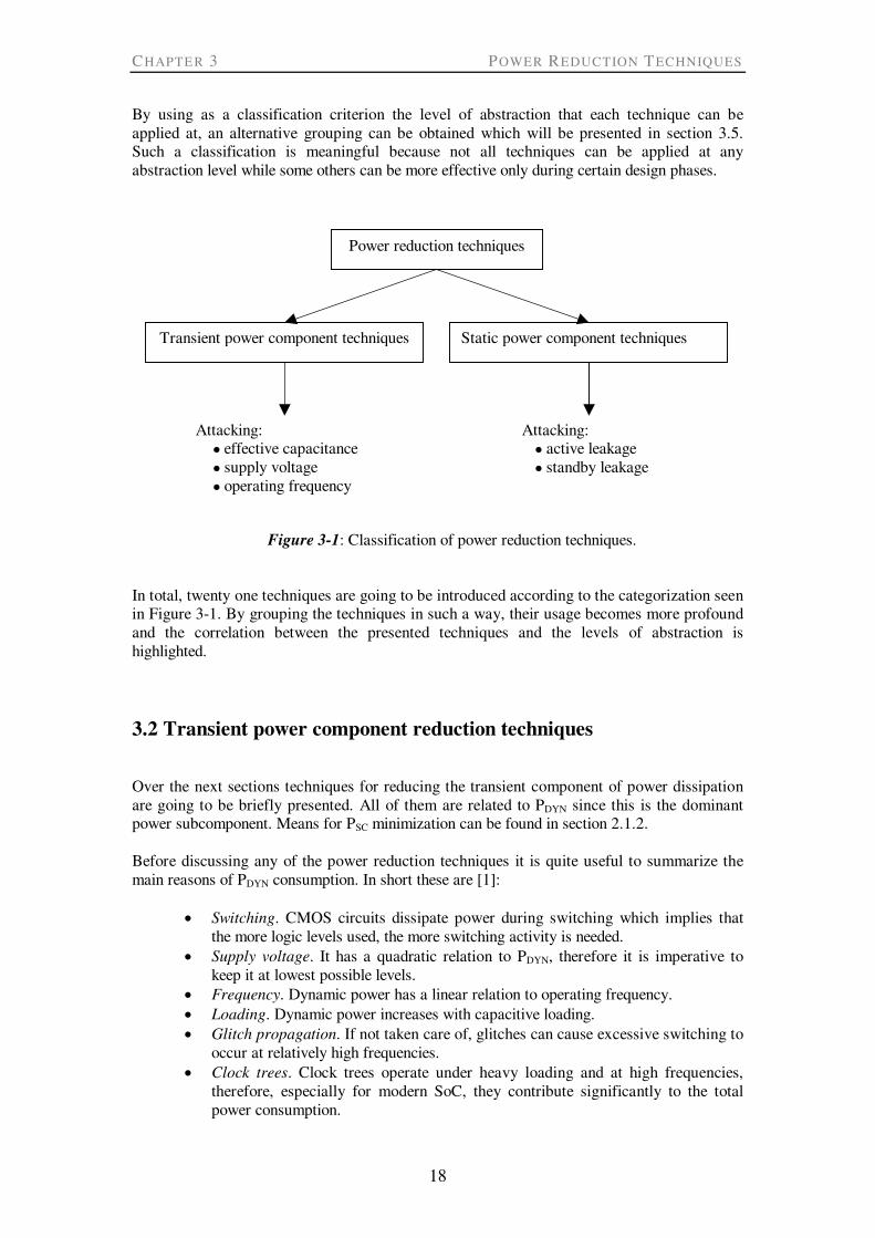
3.1 Categorization of power reduction techniques In order to effectively present the plethora of power saving techniques that exist in today’s literature, an effort has been made to classify these techniques into categories. This classification is mainly done according to power generation mechanisms that each technique is meant to attack. As explained in section 2.2, with PDYN and PLEAK being the dominant power dissipation components the vast majority of power reduction techniques focus on them. Following the previous chapter’s terminology, it is quite handy to categorize power reduction techniques into transient power component and static power component reduction techniques. As can be seen from Figure 3-1, the first group of techniques aims at cutting down on dynamic power through the reduction of effective capacitance, supply voltage and operating frequency, while the second group of techniques tries to minimize the leakage power dissipation.
CHAPTE R 3 POWER REDUCTION TECHNIQUES
18
By using as a classification criterion the level of abstraction that each technique can be applied at, an alternative grouping can be obtained which will be presented in section 3.5. Such a classification is meaningful because not all techniques can be applied at any abstraction level while some others can be more effective only during certain design phases.
In total, twenty one techniques are going to be introduced according to the categorization seen in Figure 3-1. By grouping the techniques in such a way, their usage becomes more profound and the correlation between the presented techniques and the levels of abstraction is highlighted.
3.2 Transient power component reduction techniques Over the next sections techniques for reducing the transient component of power dissipation are going to be briefly presented. All of them are related to PDYN since this is the dominant power subcomponent. Means for PSC minimization can be found in section 2.1.2. Before discussing any of the power reduction techniques it is quite useful to summarize the main reasons of PDYN consumption. In short these are [1]:
• Switching. CMOS circuits dissipate power during switching which implies that the more logic levels used, the more switching activity is needed.
• Supply voltage. It has a quadratic relation to PDYN, therefore it is imperative to keep it at lowest possible levels.
• Frequency. Dynamic power has a linear relation to operating frequency. • Loading. Dynamic power increases with capacitive loading. • Glitch propagation. If not taken care of, glitches can cause excessive switching to
occur at relatively high frequencies. • Clock trees. Clock trees operate under heavy loading and at high frequencies,
therefore, especially for modern SoC, they contribute significantly to the total power consumption.
Power reduction techniques
Transient power component techniques
Static power component techniques
Attacking: ● effective capacitance ● supply voltage ● operating frequency
Attacking: ● active leakage ● standby leakage
Figure 3-1: Classification of power reduction techniques.

3.2 TRANSIENT POWER COMPONENT REDUCTION TECHNIQUES
19
It becomes obvious that the aforementioned reasons can be largely cancelled out, by eliminating redundant power consuming activity and scaling the voltage. That can generally be done at higher levels of abstraction and at many different parts of a design, e.g. its datapath, clock tree, busses, FSMs etc. 3.2.1 Operator selection for low power Arithmetic operators, such as adders and multipliers, make up the basic building blocks of common datapath components. As such, they are of great importance for low power design being so commonly used and such a critical part of the datapath. When it comes to selecting an arithmetic operator certain aspects have to be considered. Profoundly, effective capacitance should be minimized which in turn is a function of the operator’s architecture, area, number of logic levels, fanout distribution and possible signal encoding. Glitches can also add up to an operator’s power dissipation. Usually a high fanout along with a large number of logic levels implies higher glitch propagation. A common set of adders is the one including the ripple carry (RPL), forward carry look ahead (CLF), carry look ahead (CLA) and the Brent-Kung (BK) adders. Ripple carry adders may be attractive for their small size but the carry signal propagates through all the stages thus consuming power. This occurs to a lesser extent in CLA and CLF adders, but at the cost of higher number of logic levels. The best option for area, speed and power tradeoff is the BK adder [1]. The Brent-Kung adder is a parallel prefix adder that was originally proposed as a simple and area efficient adder. It offers a good architecture for minimizing the number of logic levels, wiring tracks, fanout, and gate count [2]. As for multipliers, Wallace advantages over carry-save multiplier due to its uniform switching propagation, less logic levels and lower average fanout [1]. More power savings can be accomplished by utilizing special kinds of signal encoding like the Hybrid encoding [3], which is a compromise between the minimal input dependency offered by the binary encoding and the low switching characteristics of the Gray encoding. Operators are usually inferred from HDL code and their actual implementation is selected by synthesis tools, according to which one best meets the design constraints. It is therefore important to know the properties of each operator’s possible architectures, thus being able to instruct the tools which one to select out of the list when it comes to low power design. 3.2.2 Precomputation Precomputation is a logic optimization technique that aims at lowering logic transitions by selectively preevaluating the output values of a logic function one clock cycle before they are required, and then using the preevaluated values to reduce internal switching activity in the succeeding clock cycle. This concept can be further explained by taking the circuit in Figure 3-2 as an example. In this figure the Subset Input Disabling architecture of precomputation is shown [4]. By identifying a logic condition on some inputs of combinational block CL for which the output does not vary, we can partition the inputs into two sets, precomputed and gated, corresponding to the registers R1 and R2. For the two boolean functions g1 and g2, which are called predictor functions, it is required that: g1 = 1 => f = 1 and g2 = 1 => f = 0. If, during a clock cycle, either g1 or g2 is set then register R2 is disabled for the next clock cycle thus freezing the gated inputs. Precomputation inputs are updated, hence the output evaluates to the correct logical value. Because only a subset of the block’s inputs change, less switching activity is manifested. This stands true only if the switching overhead caused by the predictor functions

CHAPTE R 3 POWER REDUCTION TECHNIQUES
20
is less than the switching avoided by disabling R2. Therefore, the choice of g1 and g2 is critical since we need to maximize their probability of evaluating to 1 and at the same time to maintain a considerably smaller complexity than f. Such a choice is not unique but a result of tradeoff between area/delay overhead and achievable power reduction.
Figure 3-2: Subset Input Disabling precomputation architecture The issue of not being able to precompute any input combination, due to the constrained precomputation input subset of the previous architecture, is alleviated by the introduction of the Complete Input Disabling precomputation architecture proposed in [5]. In that architecture precomputation logic can be a function of all input variables, allowing the precomputation of any input combination. Experimental results showed significant power reductions over both original circuits as well as those synthesized under the latter architecture. A precomputation architecture for multioutput circuits is also possible at the expense of being significantly more complex and with oversized predictor functions. 3.2.3 Guarded evaluation Guarded evaluation [6] is a gate level power optimization technique that relies on blocking the inputs of complex datapath circuits for transition reduction, if these inputs do not contribute to output generation for a given sensitization vector. In other words, if under certain conditions a fanout is not observed, that is, if it has observable don’t care (ODC) conditions, then transparent latches or floating gates can be inserted at the corresponding fanin. Such parts of the datapath are denoted as guarded. Usually multiplexers generate ODC conditions. Whenever an input vector belonging to the guarded logic ODC set appears, the guarding logic does not allow any signal transitions pass through the guarded logic. This architecture is illustrated in Figure 3-3. An interesting trait of this technique is that the entire circuit need not be resynthesised to find out the possibilities as to when it is applicable. The evaluation of the guarding logic is guarded by already existing signals and power optimization is obtained by including a transformation circuitry to the original circuit. This technique is most common in the design of datapath functions in low power processors.

3.2 TRANSIENT POWER COMPONENT REDUCTION TECHNIQUES
21
Figure 3-3: Guarded Evaluation architecture 3.2.4 Operand Isolation In a datapath intensive design, the complex combinational blocks may contribute to the majority of power consumption of the design. Operand isolation [7] is based on the same principle as guarded evaluation but with this technique designs described at the register transfer level (RTL) are processed. By taking advantage of ODC conditions an RTL exploration can be done for identifying circuit portions which perform redundant computations, thus suppressing switching activity. An example is illustrated in Figure 3-4. As seen, the output of the adder is observed at the DFF input only when selA is “1” and selB is “0”. Therefore, the isolation logic added consists of a control signal OI_En and some gates. The inputs to the adder are enabled by OI_En = (selA AND (NOTselB)).
Figure 3-4: Example of Operand Isolation application In this technique guarding logic doesn’t have to exist independently in a circuit. It may be hidden in complex arithmetic blocks of the RTL model or not even present at all. By acting on the register transfer level, arbitrary logic can be transformed into multiplexer-based logic, thus taking advantage of the brought out ODC conditions during synthesis for conditional evaluation and/or propagation.

CHAPTE R 3 POWER REDUCTION TECHNIQUES
22
3.2.5 Operator Reduction Operator reduction is a technique based on transformations of operations into computationally equivalent implementations at the algorithmic level. Its objective is to optimize the number and type of computational modules, their interconnection and their sequencing of operation, while input/output behavior is preserved. This is an apparent approach for reducing the effective capacitance in a circuit. As an example we can consider the algebraic expression (X*Y) + (Z*Y) which, by using distributive multiplication over addition, can be rewritten as (X+Z)*Y. Its straightforward implementation, shown in Figure 3-5(a), requires two multiplications and one addition and has a critical path of two control cycles. On the other hand, the transformed expression’s implementation, Figure 3-5(b), requires one less multiplication maintaining the same critical path. It is obvious that the latter is an optimized implementation.
Figure 3-5: (a) Straightforward implementation (b) Operator Reduction applied
There are cases that a reduced number of operators can be achieved at the cost of a longer critical path. This implies a higher supply voltage if we want a realization that retains the initial throughput. Thus, this technique can have side effects as well making the associated power minimization task a tradeoff problem. Operator reduction is one of the techniques belonging to the High-level Synthesis Transformations set, along with operation substitution, wordlength reduction, control step reduction etc. More on these can be found in [8]. 3.2.6 Data Representation The switching activity from a datapath element is directly proportional to the number of bits switched between successive data accesses. Therefore, an optimized style for data representation could result in lower switching activity. In [9] a method of changing data representation at a system-wide level for low power is described. The proposed method is based on the observation that the distribution of data value transitions is usually highly skewed, and exploits this observation in choosing a data representation so consecutive data value pairs that appear frequently are encoded to have a smaller Hamming distance. This implies that information regarding data value transitions for

3.2 TRANSIENT POWER COMPONENT REDUCTION TECHNIQUES
23
a target application has to be computed in advance. In order to maintain compatibility within the system between parts that use different data representations, converters are used in the datapath to change the low power representation to normal and vice versa. Authors claim a 22% reduction in switching activity for MPEG-1 decoders. Using sign-magnitude instead of two’s complement data representation can also yield power savings under certain conditions. Although for most signal processing applications two’s complement is chosen for performing arithmetic operations easy, that can have a negative impact on switching activity as explained in [10]. Sign-extension causes the MSB sign bits to switch when a signal changes values around zero. Thus, if the signals being processed frequently switch from positive to negative values without utilizing the whole bit-width, then switching activity can be significantly increased. In such cases sign-magnitude can be a good alternative for power minimization, since only one bit is allocated for the sign for this representation. In general, these techniques are quite application specific and have to be judiciously utilized. 3.2.7 Pipelining and Parallelism There is a dependency between the operating frequency of a circuit and its supply voltage given by f ~ (VDD - VTH)2 / VDD => f ~ VDD, assuming VTH << VDD. This implies that we can use performance speed-up transformations, and tradeoff performance gains for power through voltage scaling. A common method for reducing a circuit’s critical path is pipelining. The notion of pipelining is shown in Figure 3-6.
Figure 3-6: (a) Typical 16-bit addition
(b) Pipelined 16-bit addition Our example includes a 16-bit adder and two registers that provide new operands each clock cycle. Assuming a critical path delay of 10ns for the adder, the operating frequency of the circuit is, fREF = 100MHz. Thus, the estimated dynamic power of the circuit would be PREF = αCREFV
2REFfREF. By applying the pipelining method on the circuit, Figure 3-6(b), it is divided
into two stages with an 8-bit addition being performed in each stage. The critical path delay of an 8-bit adder can be considered about half of a 16-bit one, therefore the operating frequency of the pipelined circuit can go up to 200MHz doubling the throughput. We can tradeoff this extra performance for power by halving the voltage, thus retaining the application’s sufficient

CHAPTE R 3 POWER REDUCTION TECHNIQUES
24
original throughput with an extra latency cycle. If we consider a small increase in area due to the extra register, the estimated dynamic power for the pipelined circuit would be PPIP = αCPIPV
2PIPfPIP = α(1.15CREF)(VREF / 2)2fREF = 0.2875PREF.
Logically deep internal nets are typically more affected by primary input switching, therefore they are more susceptible to glitches. Pipelining can attain glitch reduction as well, since it shortens the depth of combinatorial logic by register insertion. On the other hand, it increases clock tree power but overall power consumption in a design is lowered. We can achieve significant power savings by using parallelism [11] as well, which is a method based on the same concept as pipelining. The main idea is to maintain throughput at reduced supply voltages through hardware duplication. By using parallel, identical units, the speed requirements on each unit are reduced, allowing for a reduction in the circuit’s voltage. 3.2.8 Register Retiming Register retiming is a sequential optimization technique that moves registers through the combinational logic gates of a design to optimize timing and area. This proves particularly useful when some stages of a design exceed the timing goal while others fall short. Retiming can be used for minimizing dynamic power in a twofold fashion. One way, proposed in [12], is to reduce switching activity of “busy” computational elements, specially of those who drive large capacitive loads, by moving registers to their outputs. This way outputs will change only once per clock cycle, thus masking power costly glitches. The heuristic algorithm for the selection of the candidate gates to be registered, is based on the amount of glitching that occurs at the output of each gate and the probability that this glitching can further propagate. The second approach is similar to pipelining and parallelism, retiming provides an efficient and straightforward way to reduce critical paths while preserving throughput and the number of operations. Performance gains can then be exchanged for lower supply voltage. In [13] a hybrid retiming and supply voltage scaling technique is proposed. The authors not only scale down the voltage of computational elements that are out of the critical paths but also, through retiming, try to move registers around in order to maximize the number of elements off the critical paths, thus incurring further power savings. 3.2.9 Clock Gating Clock gating [14] is the primary means of dynamic power management in synchronous circuits. It is a very efficient technique that provides a way to selectively stop the clock, whenever the computation that is to be carried out at the next clock cycle is redundant. In other words, the clock signal is disabled according to the idle conditions of the logic network, thus evading a considerable power consumption by combinatorial logic, flip-flops and by the clock buffer tree in the design. Clock gating actually works by identifying groups of flip-flops, which share a common enable term that determines when a new value is to be clocked into the flip-flops. The implementation of clock gating mechanism can be as a simple as an AND or an OR gate, depending on the edge on which flip-flops are triggered. Due to the fact that such a simple implementation is susceptible to hazards/glitches of the enable term that could corrupt the clock signal to the registers, a transparent latch is usually inserted between the glitchy enable term and the AND/OR gate.

3.2 TRANSIENT POWER COMPONENT REDUCTION TECHNIQUES
25
Some drawbacks of clock gating are that it may hinder timing closure and can make design for testing and verification more complex. The design of highly testable, gated clock circuits is discussed in [15]. Overall, the clock gating technique is very advantageous for circuits that are often idle for long periods and get activated by request. 3.2.10 Gated-clock FSM As with arithmetic operators, finite-state machines (FSM) are also very common parts of digital systems used to generate signal sequences, to check an signal sequences or to control large datapath parts. It is therefore imperative to try to minimize their power consumption. The basic structure of a FSM (Moore machine) is shown in Figure 3-7. It can be observed that power can be consumed either in the logic blocks, that generate the next state and the outputs, or in the clock distribution to the flip-flops of the state register.
Figure 3-7: A generic Moore machine The basic idea of gated-clock FSM [16] is to avoid any redundant switching activity in the next state logic block and in the state register, if the FSM present state is the same as the next one. Put differently, this technique discusses the application of clock gating in finite state machines. This concept is demonstrated in the example of Figure 3-8 [17].
Figure 3-8: Example of a potential gated-clock FSM We assume that the depicted state machine interacts with a timer in order to implement a very long delay of thousands of clock cycles before executing a complex but very short operation. By using clock gating, it is possible to avoid dynamic power dissipation during the timer’s countdown phase by freezing both the clock and the inputs of the FSM. We can use the

CHAPTE R 3 POWER REDUCTION TECHNIQUES
26
timer’s flag ZERO as the enable signal for the clock gating logic. Further power savings could also be achieved by masking the inputs and/or the clock of the datapath that the FSM controls, if its outputs are not used during countdown. This technique can be proven very useful in reducing dynamic power, if it’s used effectively according to the RTL designer’s experience in identifying and extracting the busy parts of a FSM and clock gating the rest of idle logic. 3.2.11 FSM state encoding Efficient encoding of the states of a FSM can help reducing power consumption in the next state and output combinatorial blocks, by suppressing logic transitions. The main idea is to use an encoding scheme that minimizes switching from one state to another, if such a transition is very likely to happen. Table 3-1 verifies this concept.
TABLE 3-1 COMPARISON OF THREE COMMON STATE ENCODING STYLES
State One Hot Gray Binary
S0 00000001 000 000 S1 00000010 001 001 S2 00000100 011 010 S3 00001000 010 011 S4 00010000 110 100 S5 00100000 111 101 S6 01000000 101 110 S7 10000000 100 111
Total # of transitions 16 8 11 Max. transitions per
clock cycle
2 1 3
Flip-Flops (clock load) 8 3 3
If we identify the most probable cycles in a FSM and encode the states on these cycles with minimum Hamming distance codes, then power dissipation can also be minimized. In general this is not an undemanding task since special tools that propagate transition probabilities on the FSM inputs and calculate the probability of each transition are required. There are cases though where this technique could be more easily applied. In the example depicted in Figure 3-9 [17], states from RESET to S29 are chained sequentially with 100% probability of transition. Therefore, a gray encoding is the best choice. If we assume that condition C0 has a much lower probability than C1, the gray encoding should not be incremented from S29 to S30 and S31. Attention should be paid though not to lose what is gained in the next-state logic in the output logic activity. Usually a good choice is One Hot encoding for FSM with less than 8 states in order to optimize area, speed and power [18]. It is usually the preferred encoding for large FPGA-based state machine implementations though [19]. Otherwise, a good practice is to group states that generate the same output and assign them codes with minimum Hamming distance (see example in [17]). Overall, designing a FSM is a challenging task that requires tradeoffs and even case-by-case analyses in order to find an optimal, power efficient solution.

3.2 TRANSIENT POWER COMPONENT REDUCTION TECHNIQUES
27
Figure 3-9: FSM for which gray encoding should be used for low power 3.2.12 FSM partitioning The basic idea of FSM partitioning is to decompose a large finite state machine into two or more simpler machines that jointly produce the equivalent input-output behavior, as the original machine, for low power purposes [20, 21]. The new sub-FSM will be composed of smaller state registers and combinatorial logic blocks. The technique is meaningful if the original, bulky FSM is partitioned by searching for a small subset of states with high probability of transitions among them and a low probability of transitions to and from other states. The high transition activity subset of states will constitute a small sub-FSM that is consequently active most of the time. Therefore, such a partition enables the application of clock gating on the larger, and most of the time inactive, sub-FSM thus saving dynamic power. The technique can be further illustrated with the simple example of Figure 3-10 [17].
Figure 3-10: (a) An example of a large FSM with a subroutine (b) By partitioning, each idle sub-FSM can be clock and input gated
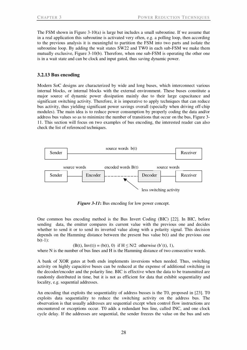
CHAPTE R 3 POWER REDUCTION TECHNIQUES
28
The FSM shown in Figure 3-10(a) is large but includes a small subroutine. If we assume that in a real application this subroutine is activated very often, e.g. a polling loop, then according to the previous analysis it is meaningful to partition the FSM into two parts and isolate the subroutine loop. By adding the wait states SW22 and TW0 in each sub-FSM we make them mutually exclusive, Figure 3-10(b). Therefore, when one sub-FSM is operating the other one is in a wait state and can be clock and input gated, thus saving dynamic power. 3.2.13 Bus encoding Modern SoC designs are characterized by wide and long buses, which interconnect various internal blocks, or internal blocks with the external environment. These buses constitute a major source of dynamic power dissipation mainly due to their large capacitance and significant switching activity. Therefore, it is imperative to apply techniques that can reduce bus activity, thus yielding significant power savings overall (specially when driving off-chip modules). The main idea is to reduce power consumption by properly coding the data and/or address bus values so as to minimize the number of transitions that occur on the bus, Figure 3-11. This section will focus on two examples of bus encoding, the interested reader can also check the list of referenced techniques.
Figure 3-11: Bus encoding for low power concept.
One common bus encoding method is the Bus Invert Coding (BIC) [22]. In BIC, before sending data, the emitter compares its current value with the previous one and decides whether to send it or to send its inverted value along with a polarity signal. This decision depends on the Hamming distance between the present bus value b(t) and the previous one b(t-1):
(B(t), Inv(t)) = (b(t), 0) if H ≤ N/2 otherwise (b’(t), 1), where N is the number of bus lines and H is the Hamming distance of two consecutive words. A bank of XOR gates at both ends implements inversions when needed. Thus, switching activity on highly capacitive buses can be reduced at the expense of additional switching in the decoder/encoder and the polarity line. BIC is effective when the data to be transmitted are randomly distributed in time, but it is not as efficient for data that exhibit sequentiality and locality, e.g. sequential addresses. An encoding that exploits the sequentiality of address busses is the T0, proposed in [23]. T0 exploits data sequentiality to reduce the switching activity on the address bus. The observation is that usually addresses are sequential except when control flow instructions are encountered or exceptions occur. T0 adds a redundant bus line, called INC, and one clock cycle delay. If the addresses are sequential, the sender freezes the value on the bus and sets
encoded words B(t)
source words b(t) Sender Receiver
Sender Receiver Encoder Decoder
source words source words
less switching activity

3.2 TRANSIENT POWER COMPONENT REDUCTION TECHNIQUES
29
the INC line. Otherwise, INC is deasserted and the original address is sent. With T0 code, power savings are maximized if the probability of sequential addresses appearing on the bus is high. An example of both the BIC and T0 codes is shown in Table 3-2.
TABLE 3-2 EXAMPLE SHOWING THE EFFICIENCY OF BIC AND T0 CODES
Binary Source
Word Trs. BIC word Trs.
Binary Source
word Trs. T0 code word Trs.
00101010 - 00101010 - - 00000100 - 00000100 - - 00111011 2 00111011 0 2 00000101 1 00000100 1 1 11010100 7 00101011 1 2 00000110 2 00000100 1 0 11110100 1 11110100 1 1 00000111 1 00000100 1 0 00001101 6 00001101 0 3 00001000 4 00000100 1 0 01110110 6 10001001 1 3 00000110 3 00000110 0 2 00010001 5 00010001 0 4 00000111 1 00000110 1 1 10000100 4 10000100 0 4 00001000 4 00000110 1 0
Total transitions 31 19 16 4
Several methods that are combinations of the BIC and T0 encodings are proposed in [24]. In [25], an encoding technique based on the notion of self-organizing lists is proposed. In [26], a class of irredundant low power techniques is introduced, for encoding instruction or data source words before they are transmitted over buses. In [27], the authors provide a modified BIC (MBI) technique which besides reducing delay and power also minimizes the crosstalk noise that results from inductive coupling between the bus lines. In [28], the working zone method is presented. 3.2.14 Multi-VDD Design Because dynamic power is proportional to V2
DD, even a small reduction in supply voltage causes a quadratic decrease in power consumption. On the other hand, by decreasing the supply voltage the circuit’s delay is influenced negatively. Multi supply voltage design introduces the idea of preserving performance, while also reducing power consumption. This can be achieved by assigning the high VDD (VDDH) to the gates that belong to the critical path, while the lower set of supply voltages is assigned to off-critical path remaining gates according to their timing slack. If only two different supply voltages are provided, VDDH and VDDL, the technique is simplified into dual-VDD design. To avoid excessive static power dissipation, due to the inability of VDDL gates completely cutting off driven VDDH gates, the use of level converters placed between the VDDL and VDDH supplied gates is necessitated, which imposes area and power overheads. Layout is an important issue when dealing with multi VDD designs due to different n-well voltages of different supply voltage cells. In brief, two algorithms have been proposed for optimal assignment of cells to the layout, clustered voltage scaling (CVS) [29] and extended CVS (ECVS) [30]. CVS allows only one voltage transition along a path and level conversions only at flip-flops. ECVS allows multiple voltage transitions along a path and placement of level converters even between logic cells. In general, power savings arising from the adoption of multiple supply voltages technique may be insignificant, due to the use of additional level converters, therefore dual- or triple-VDD techniques are mostly used [31]. Modern SoC have a plethora of IP blocks and sub-components integrated. Another type of multi-VDD design is based on the observation that different parts of a chip might have

CHAPTE R 3 POWER REDUCTION TECHNIQUES
30
different speed requirements. For example, the CPU and RAM blocks might need to be faster than a simple peripheral block. This implies a design can be partitioned into multiple voltage domains (also referred to as “Voltage Islands” in layout), based on timing criticality. For logic blocks that can operate at low clock speeds and are not timing critical, the supply voltage can be reduced to a level that just maintains reliable operation of the block [31]. Of course level converters are needed in this technique as well, for signals travelling through different voltage domains. Generally, this is a non-trivial technique to apply on a design because of the difficulties in placing the level converters and reducing their overhead, acquiring cell libraries characterized for every operational voltage and efficiently partitioning the design for maximum power savings. A detailed knowledge of the functionality of the design is usually required. Complicated board-level design, high production costs and large energy costs outside the chip are also a big concern [32]. It should also be noted that leakage power is also reduced, to a lesser degree, by voltage scaling due to its linear variation with VDD. 3.2.15 Dynamic Voltage and Frequency Scaling Dynamic Voltage and Frequency Scaling (DVFS) [33], is an adaptive “version” of the previously discussed static Multi-VDD design technique. It allows devices to change their components voltage and corresponding frequency during runtime to adapt to the workload demand. DVFS can be applied to different levels of granularity, on large modules or even on individual logic blocks on the critical path at the expense of complexity overheads [34]. This is an advanced technique that requires proper software and hardware cooperation and is usually correlated with processors, since these components are extensively used within embedded systems and are power hungry. Obviously, DVFS results in processors with variable performance. The technique is based on the key observation that a processor’s peak performance isn’t always required (large positive slacks), therefore the processor (or any other relevant hardware component) can be safely slowed down to save power, on the fly. Variable performance can be made unnoticeable to the end-user by accurately predicting the upcoming workload requirements and then adjusting the processor’s voltage and frequency accordingly. A typical example is mentioned in [35]. If we consider a task with a deadline of 25 ms running on a processor with a 50MHz clock speed and 5.0 V supply voltage then if the task requires 5×10⁵ cycles for its execution, the processor executes the task in 10 ms and becomes idle for the remaining 15 ms. However, if the clock speed and the supply voltage are lowered to 20 MHz and 2.0 V, it finishes the task at its deadline, 25ms, resulting in ~84% energy reduction. Dynamically adjusting the supply voltage, so that the power consumption is minimized while not violating the timing requirements, is a property not easily accomplished in reality. This is actually the job of DVFS algorithms for voltage scheduling. For hard real-time systems, there are two types of voltage scheduling approaches [35] depending on the voltage scaling granularity: intratask DVFS (IntraDVFS) [36] and intertask DVFS (InterDVFS) [37]. The main difference between the two approaches is whether the slack times are used for the current task or for the tasks that follow. InterDVFS algorithms distribute the slack times from the current task for the following tasks, while IntraDVFS algorithms use the slack times from the current task for the current task itself [35]. To provide real-time guarantees, those algorithms need to be integrated with the OS’s real-time scheduler [38]. In addition to reducing power consumption, DVFS can provide benefits to process variations and thermal control. By employing higher voltages on the slower gates of the chip to increase performance, and using lower voltages on the faster gates to decrease leakage, variations can be compensated. The chip can be configured in so that most of the gates will exhibit uniform leakage and delay characteristics [34]. Similarly, the chip can be configured to place a limit on the maximum chip temperature at the expense of performance [39]. Characteristic examples of processors employing DVFS are AMD’s PowerNow! [40], Intel’s Xscale [41] and Transmeta Crusoe’s LongRun [42].

3.3 STATIC POWER COMPONENT REDUCTION TECHNIQUES
31
3.3 Static power component reduction techniques Although dynamic power consumption is traditionally regarded as the main power dissipation component in digital CMOS circuits, leakage is lately being brought into prominence as well, by the continuous technology nodes scaling. According to G. E. Moore, if the trend of leakage being increased for each new technology generation continues, dynamic power consumption will soon be overtaken by the leakage power [43]. A problematic property of leakage power is that as long as the power supply voltage is switched on it remains, while dynamic power consumption varies with the workload. This makes leakage power a large contributor to the overall power consumption, specially in the era of the plethora of mobile gadgets where large parts of these systems are in idle mode most of the time, thus rendering simple saving schemes such as clock gating less attractive. It becomes clear, that for effective low power design a combination of dynamic and leakage power reduction techniques is imperative.
Figure 3-12: Qualitative illustration of dynamic and leakage power dissipation. Leakage power dissipation can be analyzed into two branches based on operating modes, active and standby leakage. Active leakage occurs when overall system is operating (large workload), while standby leakage occurs when overall system is in sleep mode (no or minimal workload). Figure 3-12(a) shows a typical burst system. Dynamic power dominates during the active period, while leakage is uniform2 in both active and standby periods. The trend of lowering the supply voltage with each new technology generation has helped taming
2 Assuming a constant temperature.
PLEAK
standby period active period
PDYN
PLEAK PLEAK
PDYN
PLEAK
PLEAK
PDYN
PLEAK
(a)
(b)
(c)

CHAPTE R 3 POWER REDUCTION TECHNIQUES
32
dynamic power, though degenerating speed at the same time. In order to keep up with timing requirements, threshold voltages were also scaled down in parallel, which in turn resulted in a significant increase in the leakage current of the transistors, Figure 3-12(b). Figure 3-12(c) shows the goal of leakage power reduction techniques, suppressing the exaggerated leakage. Standby leakage can be more aggressively attacked, due to the non-existent timing requirements during idle mode. The aforementioned classification is followed for the presentation of leakage reduction techniques in this section. In general, due to standby periods being very long, e.g. a mobile phone is in standby mode most of the day, standby leakage reduction techniques are considered more important.
3.3.1 Power Gating The idea behind power gating is as simple as it gets, when a logic block is in standby mode disconnect it from the power supply to avoid wasting leakage power [44]. This can be straightforwardly achieved by using one pMOS transistor and one nMOS transistor in series with the transistors of each logic cell to create a virtual ground and a virtual power supply, Figure 3-13. The transistors being utilized for that purpose are called sleep transistors, and in practice only the nMOS sleep transistors are used for a virtual ground, due to their lower ON resistance. During the active periods sleep transistors are ON, and thus the circuit functions as usual. During the standby periods the sleep transistors are turned off, thus the virtual ground collapses and the logic cells are disconnected from the power grid.
Figure 3-13: Straightforward implementation of a power gating circuit.
Sleep transistors are not ideal switches, they are leaky too. In order to minimize their leakage sleep transistors with high voltage thresholds are used, otherwise power gating becomes less effective. In practice a dual- or multi-VTH CMOS3 technology is utilized, transistors with a
3 Multi-Threshold CMOS (MTCMOS) is commonly used as a synonym for power gating, since the most prevalent power gating implementations utilize multiple transistor thresholds. However, it is also

3.3 STATIC POWER COMPONENT REDUCTION TECHNIQUES
33
low VTH are used to implement the logic while high VTH devices are used as sleep transistors. Leakage of the sleep transistors is also proportional to the width of the transistors. Smaller sleep transistors are more effective in cutting down leakage power. On the other hand, small sleep transistors have negative impact on the circuit performance, due to large IR drops that decrease the effective supply voltage of the logic gates and also due to the increase of the threshold of the pull-down transistors because of the body effect. Using large sleep transistors can alleviate these side effects. Then again, using large sleep transistors increases the area overhead and the dynamic power consumed for switching between active and standby modes. This imposes constraints on the minimum duration of the standby periods. Frequent switching between the modes can offset leakage power savings [44]. It becomes clear that, adding a sleep transistor to every gate that is to be turned off imposes a large area and timing penalty. Thus, a tradeoff rises: minimizing the performance impact of the virtual ground results in more area overhead and lesser leakage reduction due to larger switches. A way to reduce the area consumed by the switches is to share them. This can be done in two fashions, according to the desired granularity [45]. Fine-grain power gating encapsulates the switching transistor as a part of the standard cell logic. Coarse-grained approach implements locally shared virtual power networks. Another issue that has to be taken into account by designers is the loss of the state registers’ data, when power gated, unless this is somehow prevented. Some methods for addressing this problem include power gating only combinational logic, utilizing specially designed state retention registers [46], saving the state to off-chip memory by scanning out the internal state prior to power-down [47] etc. Another drawback of using sleep transistors is that they generate noise in circuits due to charge accumulation in the virtual ground while OFF. This problem is partially addressed in [48]. Overall, power gating is a very effective method for coping with standby leakage power. However, it requires a MTCMOS process technology and suffers from the aforementioned drawbacks, i.e. performance degradation, laborious sleep transistor sizing, decreased noise margins etc.
3.3.2 Body Bias Control Changing the source-bulk voltage, VSB, can alter a transistor’s threshold voltage [49]. This is described as the body effect and in this context the substrate can be thought of as a second gate, often referred to as the “back gate”. The body effect upon the VTH of an nMOS
MOSFET is computed according to the equation4: VTHN = VT0 + γ( Fφ2VSB + − Fφ2 ),
where VTHN is the threshold voltage when substrate bias VSB is present, VT0 is the threshold voltage for zero substrate bias, ΦF is the substrate Fermi potential, and the parameter γ is the body effect coefficient. Based on the body effect, body bias control is a technique for changing the threshold voltage of transistors, thus making it possible to indirectly control their leakage and delay. This technique can be either applied at a fullchip level or at a finer granularity. Typically, a block-level approach is preferred. Body biasing works as follows. When a logic block enters the standby state, the substrate is reversely biased (reverse body bias, RBB) to increase the VTH of the transistors, thus reducing the standby leakage power dissipation [50]. When the block returns to the active state, RBB is removed, thus restoring the nominal VTH, power dissipation and performance of the transistors. It should be noted that in order to apply reverse body biasing to pMOS transistors their substrate voltage (n-well voltage) has to be raised above VDD. This requires a triple-well technology, which may not always be available. It is also possible to forward bias the bulk
used to refer to another leakage power reduction technique that utilizes multiple transistor thresholds as well, see following sections. 4 Accurate for old technologies.

CHAPTE R 3 POWER REDUCTION TECHNIQUES
34
(FBB), thus reducing the VTH [51]. That’s an alternative way to save power by using high-VTH devices and applying a zero substrate bias during standby mode for low leakage, while applying FBB during active mode to decrease the gate delays and meet timing constraints. Both approaches require a control loop to provide the appropriate substrate biases based on the operation state of the functional block. The body bias control technique has an advantageous trait; it is unnecessary to save the state of the logic before entering the standby mode. On the negative side, body bias control suffers from certain drawbacks. One of them is effectiveness. Bringing the voltage of nMOS bulk below zero volts decreases ISUB, but it increases IREV and IGIDL. To avoid this, RBB should be constrained within a limited range of change of threshold voltages, which in turn limits the amount of subthreshold leakage reduction, thus rendering the technique less effective (specially with each technology generation) [52]. In general, utilizing sleep transistors yields more power savings. Additional overheads of this approach include area cost in the control loop and energy cost in charging and discharging the large substrate capacitance each time the block enters or leaves the standby mode. Similar to power gating, standby periods should be kept long enough to justify power savings. Dynamic body biasing can also be employed based on workload and software-hardware cooperation, as in DVFS [53]. It is possible to be applied along with DVFS [54]. Adaptive body biasing (ABB), which is a combined RBB and FBB technique, can provide benefits to process variations like die-to-die and intra-die variations, thus increasing VLSI chips’ acceptance rates and profit [55]. Several different types of ABB exist that resolve different kinds of variation problems [56]. 3.3.3 Minimum Leakage Vector
The Minimum Leakage Vector (MLV) technique is based on the observation that a CMOS logic gate’s leakage power dissipation is a strong function of its corresponding input values. This is due to the different number of OFF transistors in the nMOS and pMOS networks of a logic gate for different input values. Thus, given a multi-gate logic circuit, by using a pre-found minimum leakage vector to drive the circuit the combinational logic can be forced into a low leakage state during idle periods. Table 3-3 shows the leakage current of a two-input NAND gate, built in a 0.18µm CMOS technology with a 0.2V threshold voltage and a 1.5V supply voltage. As can be seen from the table’s values the minimum leakage current of the NAND gate corresponds to the case when both its inputs are zero. In this case, both transistors in the nMOS network are OFF, while both pMOS transistors are ON. This in turn corresponds to the maximum possible effective resistance between the supply and the ground, due to the two nMOS transistors being OFF in series5. It is easy to understand why the maximum leakage current corresponds to both inputs being one; the nMOS transitors are ON and the minimum effective resistance results from the parallel resistances of the OFF pMOS transistors. In any other case the leakage current value lies somewhere in between6. A similar leakage current dependency is exhibited by other logic gates as well, with respect to the applied input pattern. For example, for circuits in the MCNC91 benchmark suite the ratio of the maximum to the minimum leakage varies from 1.5 to 6 [57].
5 This phenomenon, whereby the leakage current through a stack of two or more OFF transistors is significantly smaller than a single device leakage, is called the “stack effect” [44]. 6 The small difference between the leakage current of the X=0, Y=1 vector and the X=1, Y=0 vector is due to the body effect.

3.3 STATIC POWER COMPONENT REDUCTION TECHNIQUES
35
TABLE 3-3 THE LEAKAGE CURRENT VALUES OF A 0.18ΜM NAND GATE [44]
Inputs Output
X Y Z
Leakage current
(nA) 0 0 1 23.06 0 1 0 51.42 1 0 0 47.15 1 1 0 82.94
There are three different approaches for applying the MLV technique. The first, that achieves a moderate reduction in leakage, doesn’t require any modification in the internal logic and just drives the circuit with a low leakage state vector during standby mode. To find such a vector, an efficient algorithm is required that determines a low leakage input vector out of random vectors [58]. Due to logic dependencies of the internal signals, driving a circuit with its MLV does not guarantee that the leakage currents of all its logic gates are at minimum values. Further reduction in leakage may be achieved by modifying the internal logic gates of a circuit to increase controllability while in standby mode. Such a method employs extra circuitry, used to force the low leakage input vector onto the combinational logic during standby, such as 2-to-1 multiplexers [57] or latches [59]. The third approach, that allows higher controllability during standby, modifies the gate cells with extra transistors that increase the stack effect and control the values of internal lines at the expense of extra delay. As shown in [57] this augmented approach can yield an additional 15-20% of leakage saving. Overall, although MLV technique is not as aggressive as power gating it is very easy to be used during logic design, specially the simple version of it, as long as there exists an efficient MLV algorithm. Also, technology scaling seems to have a positive effect on its effectiveness [44]. 3.3.4 Stack Effect-based technique Although the previous MLV technique indirectly utilizes the stack effect to reduce leakage power dissipation during standby periods, the stack effect wasn’t extensively analyzed. Before presenting this section’s technique a few details need to be provided on that. ISUB flowing through a stack of series connected transistors reduces significantly when more than one of the stack’s transistors are turned OFF. This is known as the “stack effect” [60]. It can be better understood if we revisit a two-input NAND gate, Figure 3-14. When both the nMOS transistors are OFF, voltage at the intermediate node VM is positive due to a small drain current. This in turn has the following effects: a) VGS1 becomes negative and so ISUB decreases greatly, b) VSB1 gets positive due to the body effect, thus increasing VTH1 further reducing ISUB, and c) VDS1 decreases resulting in even less subthreshold leakage current. As a combined result, the leakage of a two-transistor stack is an order of magnitude less than leakage in a single transistor. This further verifies the previous discussion about the dependency of a gate’s leakage on the inputs applied vector. The stack effect-based technique takes advantage of the stack effect straightforwardly, in an inverse concept to the MLV technique. If the input state vector of a circuit in standby mode is know a priori, then extra pMOS and nMOS transistors can be added in series with gates to increase the stack effect and reduce leakage power dissipation as a result [61]. This is done in a static manner by adding transistors in series with the pull-up or pull-down network of a gate/cell, knowing that this network is going to be OFF during standby mode. Thus, the output’s value won’t change by the addition. This resembles to a power gating technique with

CHAPTE R 3 POWER REDUCTION TECHNIQUES
36
carefully placed, fine granularity sleep transistors that allow retaining logic values during standby. If, on the other hand, attention is not paid and transistors are added in series with a network that is actually ON during standby then the output would float, thus causing problems to the fanout gates and possible extra static power dissipation. The authors in [61] report that an average of 65% reduction in the leakage can be achieved by using this method.
Figure 3-14: Stacking effect in a two-input NAND gate. So far low-leakage techniques that can be applied during standby periods have been discussed. The next two sections briefly present techniques for active leakage control, as well.
3.3.5 Dual and Multiple Threshold Cells Multiple threshold CMOS circuits, MTCMOS, mix high and low threshold voltage transistors in a single chip in order to address leakage power dissipation. The idea behind this technique is that high-VTH transistors can be assigned to non-critical paths so as to reduce leakage, while the use of lower-VTH transistors is limited for the critical paths only, to maintain performance7. Since no special leakage control transistors are required in this technique, both high performance and low leakage can be achieved without adversely impacting dynamic power or design area. Usually, insertion rate of low-VTH transistors on critical paths is less than 20% [44]. This technique can yield power savings during both active and standby periods. On the downside, MTCMOS introduces process variations between the high and low threshold transistors, and requires appropriate cell libraries and more expensive CMOS technologies for fabrication. If only two-level VTH cells are used for leakage reduction, then the technique is known as dual threshold CMOS. In real designs, because using more that two threshold voltages marginally improves the power savings [62], dual threshold technique is typically employed. 3.3.6 Long Channel Devices Generally, the electrical behavior parameters of a MOS transistor, i.e. VTH, gain β etc., depend on the width W and length L of the device. This dependency increases with feature size
7 A low-VTH cell has higher speed, but higher subthreshold leakage current. A high-VTH cell has low leakage current, but less speed.

3.4 THE IMPORTANCE OF EARLY DECISIONS
37
downscaling, due to the emerging small-channel effects [63]. One of these effects is the short- channel effect (SCE) that is observed in deep-submicron MOS processes. This effect is due to the small distance between the depletion regions under the gate, thus requiring only a very small gate voltage to create a complete depletion area [63]. In other words, SCE reduces VTH, also called VTH “roll-off”, Figure 3-15. The long channel devices technique is based on this observation and tries to achieve different threshold voltages by using different channel lengths for devices in a single chip. Longer channel lengths can be used to achieve high-VTH devices, thus saving leakage power during both active and standby periods, while shorter channels allow faster but leakier devices.
Figure 3-15: Threshold voltage roll-off for an nMOS,
figure taken from [60].
Overall, this technique can be applied in a greedy manner to existing designs in an attempt to limit the leakage currents, and compared to MTCMOS it incurs similar or lower process cost [44]. On the other hand, long channel lengths for the high VTH transistors increase the gate capacitance, which in turn negatively impacts both performance and dynamic power. Controlling the threshold voltage for feature sizes less that 100nm is a non-trivial task as well [64]. Due to the up-sizing of long channel devices, leakage power dissipation savings might be offset by excess dynamic power consumption. Therefore, a judicious insertion strategy has to be observed along with the activity factor taken into account when choosing gates whose transistor lengths are to be increased. 3.3.7 Summary of the presented power reduction techniques Throughout the previous sections, a total of twenty-one power optimization techniques and principles have been discussed. Table 3-4 provides a summary of all these techniques, by listing them according to the classification explained in section 3.1.
3.4 The importance of early decisions As power consumption is becoming the new metric for competitiveness in high-end SoC markets, designers try to tame it by using power reduction techniques at various abstraction layers, according to the final results they pursue. Where and when to apply power reduction strategies is simply answered, as early as possible and at the highest possible abstraction level [65]. The justification is intuitive; it is common ground that power analysis and optimization during the early design phases at high abstraction levels can lead to large power savings. After synthesis, optimization opportunities are circumscribed by the design being committed to a

CHAPTE R 3 POWER REDUCTION TECHNIQUES
38
TABLE 3-4 SUMMARY OF THE PRESENTED POWER REDUCTION TECHNIQUES
CMOS Power Dissipation Control Techniques8
PLEAKAGE Control PDYNAMIC
Control Active Leakage Standby Leakage
Operator Selection for low power Long Channel Devices Power Gating Precomputation Multiple Threshold Cells Body Bias Control
Guarded Evaluation Minimum Leakage Vector Operand Isolation Stack Effect-based technique
Operator Reduction Data Representation
Pipelining and Parallelism Register Retiming
Clock Gating Gated-clock FSM
FSM State Encoding FSM Partitioning
Bus Encoding Multi-VDD Design
Dynamic Voltage and Frequency Scaling specific technology and their impact is hampered. The crucial role of early power estimation becomes evident as well, in order for the designers to be able to explore the design space quickly and to compare multiple micro-architecture candidates early in the design cycle. Unfortunately, there's a primary trade-off between computational complexity and accuracy for power estimations. At higher levels, power estimations have limited accuracy but are fast, whereas at lower levels, such as gate and transistor level, they are very accurate but time consuming especially for modern SoC complexities. Figure 3-16 shows the power savings attainable at various abstraction levels versus estimation accuracy [66].
Figure 3-16: Power savings and accuracy attainable at different abstraction levels.
8 For PSHORT-CIRCUIT and PSTATIC reduction principles, review sections 2.1.2 and 2.1.3 respectively.

3.5 ALTERNATIVE CLASSIFICATION OF POWER REDUCTION TECHNIQUES
39
In general, to reach low-power targets, SoC designers have to take a top-down approach beginning at the system level, moving down to architectural/algorithm level, continuing through RTL analysis and optimization, to power sign-off. At the system level the designer decides on efficient partitioning, data representation, possible power states and operation modes that can enable advanced techniques that lead to tremendous savings, like DVFS (hardware-software interaction), ABB, and power gating. Such system level decisions allow for a frame of algorithms and architectures that can be selected at the algorithm level. Over the last years, several high-level synthesis tools have incorporated comprehensive sets of transformations for area and throughput optimization coupled with power reduction techniques as well [67, 68], allowing for further optimization with concurrency (i.e. pipelining, parallelism), complexity, etc. down to RTL. The designer should explore a large part of the design space for low-power micro-architectures, during these early phases. Reaching RTL is the point where both the micro-architectural context that determines the "big picture" of power consumption, and the structural detail necessary for reasonably accurate analysis have been rendered [69]. Thus, RTL is the prime level at which architecture and the effects of power reduction techniques such as clock gating, power gating, voltage islands, bus encoding, operand isolation etc. can be estimated. It is also the point in the design flow at which effective remedial action can be taken with minimal adverse effects on design time. Most designers still develop at RTL due to the maturity of tools and flows that come along with it, with a theoretically expected power savings impact of 40% [65] or even as high as 80% [69]. Before synthesizing it is always a good practice to perform power regression9 tests as well, for verifying that power specifications are met and evaluating the best possible combination of techniques and module implementations for minimal power. After the design is committed to a specific technology and timing information are available, a handful of techniques can further optimize the netlist’s power dissipation, usually trading off slack or taking care of leakage. A problematic design though cannot be “saved” at this point. It should also be added that lately more and more designers start using SystemC as System/HDL, thus corresponding power estimation tools have also emerged. One of these is the PK_Tool [70], which is a SystemC/C++ environment dedicated to the high level estimation of energy consumption for digital systems described in SystemC. It can be used for very early regression tests and final power predictions as well, given some knowledge of the target libraries. The main goal of this section is to underline the importance of deciding early on coping with power dissipation. Early attention to power consumption is necessary for maximum power savings. After all, the techniques that have been presented are only as effective as the micro-architecture to which they are applied.
3.5 Alternative classification of power reduction techniques As discussed in section 3.1, an alternative power reduction techniques classification can be obtained based on the abstraction level criterion. Table 3-5 provides a correlation of the presented power reduction techniques with the various levels of abstraction, thus indirectly highlighting each technique’s expected impact and best design phase of application. Also it clarifies which techniques can be potentially combined during a given design phase.
9 Power regression test is a method of selecting the lowest power module from a set of otherwise functionally equivalent modules.

CHAPTE R 3 POWER REDUCTION TECHNIQUES
40
TABLE 3-5 CLASSIFICATION OF THE PRESENTED TECHNIQUES ACCORDING TO LEVEL OF APPLICATION
In Chapter three a plethora of power reduction techniques has been briefly presented, and an effort was made to interrelate those techniques with the various levels of abstraction. Also, some general principles for low power flows have been laid with emphasis being placed on coping with power early in these flows. Next chapter discusses some background on power estimation for cell based ASIC designs, and presents the power analysis flows implemented with Synopsys tools, used for the rest of the thesis.
3.6 References [1] Jonathan Alexander, “VHDL Design Tips and Low Power Design Techniques”, ppt
presentation, Actel Corporation, MAPLD 2004, last accessed 04.05.2009,
http://klabs.org/mapld04/tutorials/vhdl/presentations/low_power_techniques.ppt
[2] Brent, Kung, “A Regular Layout for Parallel Adders”, IEEE Trans. on Comp., vol C-31,
No. 3, 1982, pp. 260-264.
[3] Eduardo Costa, Sergio Bampi, José Monteiro, “FIR filter design using low power
arithmetic operators”, 2007.
[4] Mazhar Alidina, Jose Monteiro, Srinivas Devadas, Abhijit Ghosh, and Marios Papa-
efthymiou. Precomputation-based sequential logic optimization for low power. In Inter-
national Workshop on Low Power Design, pages 57–62, April 1994.
[5] J. Monteiro, J. Rinderknecht, S. Devadas, and A. Ghosh, "Optimization of Combinational
and Sequential Logic Circuits for Low Power Using Precomputation", 1995 Chapel Hill
Conference on Advanced Research in VLSI, pp. 430-444, Chapel Hill, North Carolina, March
1995.

3.6 REFERENCES
41
[6] V. Tiwari, S. Malik and P. Ashar. “Guarded evaluation: Pushing power management to
logic synthesis/design”. In Proceedings of the 1995 International Symposium on Low Power
Design, pages 221–226, November 1995.
[7] M. Munch, B. Wurth, R. Mehra, J. Sproch, and N. Wehn, “Automating rt-level operand
isolation to minimize power consumption in datapaths”, Proc. Design, Automation and
Testing in Europe, March 2000.
[8] A. P. Chandrakasan, M. Potkonjak, R. Mehra, J. Rabaey, and R. Brodersen, “Optimizing
power using transformations”, IEEE Trans. Computer-Aided Design, vol. 14, pp. 12-31, Jan.
1995.
[9] Sunghwan Kim, Jihong Kim, "Low-power data representation", Electronics Letters,
Vol.36, No.11, pp. 958-959, May 2000.
[10] Chandrakasan, AP, “Ultra Low Power Digital Signal Processing”, Proceedings of Ninth
International Conference on VLSI Design, pg 352, 1996.
[11] Sreekumar Menon, “Parallelism in circuits using duplication logic”, ppt slides,
www.eng.auburn.edu/~vagrawal/COURSE/E6270_Fall07/PROJECT/MENON/lp1.ppt, last
accessed 05.05.2009.
[12] J. Monteiro, S. Devadas, and A. Ghosh, “Retiming sequential circuits for low power,” in
Proc. Int’l. Conf. Computer-Aided Design, Santa Clara, CA, Nov. 1993, pp. 398–402.
[13] N. Chabini and W. Wolf, "Reducing Dynamic Power Consumption in Synchronous
Sequential Digital Designs Using Retiming and Supply Voltage Scaling" IEEE Trans. on
VLSI Systems, vol. 12, no. 6, June 2004, pp.573-589.
[14] L. Benini, P. Siegel, and G. De Micheli, “Automatic synthesis of gated clocks for power
reduction in sequential circuits,” IEEE Design Test Computer Magazine, vol. 11, no. 4, pp.
32–40, 1994.
[15] L. Benini, M. Favalli, and G. De Micheli, “Design for testability of gated-clock FSM’s,”
in Proc. European Design and Test Conf., Paris, France, Mar. 1996, pp. 589–596.
[16] L. Benini and G. DeMicheli, “Transformation and synthesis of FSM for low-power and
gated-clock implementation”, ACM/SIGDA ISLP ’95, Apr. 1995.
[17] Christian Piguet, “Low-Power CMOS Circuits. Technology, Logic Design and CAD
Tools”, Chpt. 11, CRC Press, 2006.
[18] C. Tsui and M. Pedram, “Low-power state assignment targeting two and multi-level
logic implementation”, ACM/IEEE Int. Conf. on CAD, pp. 82–87, Nov. 1994.
[19] Xilinx Corp., “Architecture Specific HDL Coding Styles for Spartan-II, Virtex, Virtex-E,
Virtex-II, and Virtex-II Pro”, http://www.xilinx.com/itp/xilinx4/data/docs/sim/vtex9.html, last
accessed 07.05.2009.
[20] L. Benini, G. DeMicheli, and F. Vermulen, “Finite-state machine partitioning for low
power”, IEEE ISCAS ’98, pp. 5–8, May 1998.

CHAPTE R 3 POWER REDUCTION TECHNIQUES
42
[21] S-H. Chow, Y-C. Ho, and T. Hwang. “Low Power Realization of Finite State Machines
A Decomposition Approach,” ACM Trans. on Design Automation of Electronic Systems, vol.
1 no. 3, July 1996, pp.315-340.
[22] M. R. Stan, W. P. Burleson, “Bus-Invert Coding for Low Power I/O,” IEEE Trans. on
VLSI Systems, vol. 3, no. 1, Mar. 1995, pp. 49-58.
[23] L. Benini, G. De Micheli, E. Macii, D. Sciuto, C. Silvano, “Asymptotic Zero-Transition
Activity Encoding for Address Buses in Low-Power Microprocessor-Based Systems”, Proc.
Seventh Great Lakes Symposium on VLSI, pp. 77-82, Mar. 1997.
[24] L. Benini, G. De Micheli, E. Macii, D. Sciuto, and C. Silvano, “Address Bus Encoding
Techniques for System-Level Power Optimization,” Proc. Design Automation and Test in
Europe, pp. 861-866, 1998.
[25] M. Mamidipaka, D. Hirschberg, N. Dutt, “Low Power Address Encoding Using Self-
Organizing Lists,” in Proc. Intl. Symp. on Low Power Electronics and Design, 2001, pp. 188-
193.
[26] Y. Aghaghiri, F. Fallah, and M. Pedram, “Transition reduction in memory buses using
sector-based encoding techniques,” IEEE Trans. on Computer-Aided Design, Vol. 23, No. 8,
Aug. 2004, pp. 1164-1174.
[27] M. Lampropoulos, B.M. Al-Hashimi, P.M. Rosinger, “Minimization of Crosstalk Noise,
Delay and Power Using a Modified Bus Invert Technique,” Proc. Design Automation and
Test in Europe, 2004, pp. 1372-1373.
[28] E. Musoll, T. Lang, and J. Cortadella, “Exploiting the Locality of Memory References to
Reduce the Address Bus Energy”, in Proc. Int’l Symp. on Low Power Electronics and Design,
1997, pp. 202-207.
[29] K. Usami and M. Horowitz, “Clustered voltage scaling technique for low-power design”,
Proc. Int. Symp. on Low-Power Design, Apr. 1995, pp. 3–8.
[30] K. Usami and M. Igarashi, “Low-power design methodology and applications utilizing
dual supply voltages”, Proc. Asia and South Pacific Design Automation Conf., Jan. 25–28,
2000, Yokohama, Japan, pp. 123–128.
[31] Kajin Shi and Neel Desai, "Advanced Dynamic Power Reduction Techniques: Operand
Isolation, Operand Pre-Computation and Multi-VDD", Synopsys whitepaper, Power hungry?
series, 2009.
[32] Ron Wilson, “Multi-voltage low-power design: someone has to pay the piper”,
Electronics Design, Strategy News, March 2007, last accesed 10.05.2009,
http://www.edn.com/blog/1690000169/post/870007887.html?industryid=48879.
[33] Yoshifumi Ikenaga, “Using dynamic voltage and frequency scaling to conserve system
battery power requirements”, DSPDesignLine, Sept. 2007, last accessed 12.05.2009,

3.6 REFERENCES
43
http://www.dspdesignline.com/howto/202102450;jsessionid=DTAWCMG0XSEXOQSNDL
OSKH0CJUNN2JVN?pgno=1
[34] K. Agarwal and K. Nowka. Dynamic power management by combination of dual static
supply voltages. In Proceedings of the 8th International Symposium on Quality Electronic
Design, 2007.
[35] Wai-Kai Chen (Editor), “The VLSI Handbook, Second Edition”, Chpt. 18, 2nd edition,
CRC Press, Dec. 2006.
[36] D. Shin, J. Kim, and S. Lee, “Intra-task voltage scheduling for low-energy hard real-time
applications”, IEEE Design and Test of Computers, 18, 20–30, 2001.
[37] Y. Shin and W. Choi, “Power conscious fixed priority scheduling for real-time systems”,
Proceedings of Design Automation Conference, pp. 134–139, 1999.
[38] Padmanabhan Pillai and Kang G. Shin, “Real-Time Dynamic Voltage Scaling for Low-
Power Embedded Operating Systems”, Proc. of the 18th ACM symposium on Operating
systems principles, pp. 89 – 102, Alberta, Canada, 2001.
[39] Y. Liu, H. Yang, R. Dick, H. Wang, and L. Shang, “Thermal vs energy optimization for
DVFS-enabled processors in embedded systems”, In Proceedings of hte 8th International
Symposium on Quality Electronic Design, 2007.
[40] AMD Corporation, PowerNow! Technology, last accessed 13.05.2009,
http://www.amd.com/us-en/Processors/ProductInformation/0,,30_118_10220_10221%5E964,00.html
[41] Intel Corporation, Intel XScale Technology. http://developer.intel.com/design/intelxscale,
last accessed 13.05.2009.
[42] Transmeta Corporation, Crusoe Processor, http://en.wikipedia.org/wiki/Transmeta_Crusoe,
last accessed 13.05.2009.
[43] G. E. Moore, “No Exponential is Forever: But “Forever” Can Be Delayed!”, in
Proceedings of the IEEE International Solid-State Circuits Conference, ISSCC'03, Feb. 2003,
pp. 20-23.
[44] Farzan Fallah and Massoud Pedram, “Standby and Active Leakage Current Control and
Minimization in CMOS VLSI Circuits”, IEICE transactions on electronics, 2005, vol. 88, no4,
pp. 509-519.
[45] Anand Iyer, “Demystify power gating and stop leakage cold”, EETimes-India, Mar. 2006,
http://www.powerdesignindia.co.in/STATIC/PDF/200811/PDIOL_2008NOV06_PMNG_TA
_03.pdf?SOURCES=DOWNLOAD, last accessed 15.05.2009.
[46] Calhoun, B., et. al., “Power gating and dynamic voltage scaling,” Leakage in Nanometer
CMOS Technologies, S. Narendra and A. Chandraksan, editors, Springer, 2005.
[47] V. Zyuban and S. Kosonocky, “Low power integrated scan-retention mechanism,” Proc.
International Symposium on Low Power Electronics and Design, August 2002, pp. 98-102.

CHAPTE R 3 POWER REDUCTION TECHNIQUES
44
[48] S. Kim, S. V. Kosonocky, Stephen, and D. R. Knebel, “Understanding and minimizing
ground bounce during mode transition of power gating structures”, Proc. of the International
Symposium on Low Power Electronics and Design, August 2003.
[49] B. Van Zeghbroeck, "Principles of semiconductor Devices", Chpt. 7.4.2, 2007,
http://ecee.colorado.edu/~bart/book/contents.htm, last accessed 16.05.2009.
[50] K. Seta, H. Hara, T. Kuroda, et al., “50% active-power saving without speed degradation
using standby power reduction (SPR) circuit”, IEEE International. Solid-State Circuits Conf.,
February 1995, pp. 318-319.
[51] V. De and S. Borkar, “Low power and high performance design challenges in future
technologies”, Proc. the 10th Great Lakes Symposium on VLSI, 2000, pp.1-6.
[52] A. Keshavarzi, S. Narendra, S. Borkar, V. De, and K. Roy, “Technology scaling behavior
of optimum reverse body bias for standby leakage power reduction in CMOS IC's”, Proc.
International Symposium on Low Power Electronics and Design, August 1999, pp. 252-254.
[53] T. Kuroda, T. Fujita, F. Hatori, and T. Sakurai, “Variable threshold-voltage CMOS
technology”, IEICE Transactions. on Fundamentals of Electronics, Communications and
Computer Sciences, vol. E83-C, November 2000, pp. 1705-1715.
[54] Le Yan, Jiong Luo and Jha N.K., “Combined dynamic voltage scaling and adaptive body
biasing for heterogeneous distributed real-time embedded systems”, Computer Aided Design,
2003. ICCAD-2003. pp. 30-37.
[55] James W. Tschanz, James T. Kao, Siva G., Raj Nair, Dimitri A. Antoniadis, Anantha P.
Chandrakasan, Vivek De, “Adaptive Body Bias for Reducing Impacts of Die-to-Die and
Within-Die Parameter Variations on Microprocessor Frequency and Leakage”, IEEE Journal
of Solid-State Circuits, Vol. 37, Nov. 2002.
[56] Doug Stauber, “Adaptive Body Biasing”, lecture slides, last accessed 16.05.2009,
http://www.ece.rochester.edu/~velenis/courses/fall2006/ece530/Presentation/DougStouber.ppt.
[57] A. Abdollahi, F. Fallah, M. Pedram, “Runtime mechanisms for leakage current reduction
in CMOS VLSI circuits”, Proc. International Symposium on Low Power Electronics and
Design, August 2002.
[58] A. Abdollahi, F. Fallah, M. Pedram, “Minimizing leakage current in VLSI circuits”,
Technical Report, Department of Electrical Engineering, University of Southern California,
No. 02-08, May 2002.
[59] Halter, J.P. and Najm, F.N., “A gate-level leakage power reduction method for ultra-low-
power CMOS circuits”, In Proc. Custom Integrated Circuits Conference, 1997, Santa Clara,
USA, pp. 475-478.
[60] Kiat-Seng Yeo, Kaushik Roy, “Low-Voltage Low-Power VLSI Subsystems”, Chpt. 2, 1st
edition, McGraw-Hill, 2004.

3.6 REFERENCES
45
[61] K. Roy, et al., “Leakage Control with Efficient use of Transistor Stacks in Single
Threshold CMOS”, Proc. Design Automation Conference, June 1999.
[62] A. Srivastava, “Simultaneous Vt Selection and Assignment for Leakage Optimization”,
Proc. International Symposium on Low Power Electronics and Design, August 2003.
[63] Harry Veendrick, “Deep-Submicron CMOS ICs - From Basics to ASICs”, Chpt. 2,
Springer, 2nd edition, Dec. 2000.
[64] Y. Taur, et al., “High Performance 0.1um CMOS devices with 1.5V power supply”, Proc.
International Electron Devices Meeting, 1993, pp. 127-130.
[65] “Digital ASIC Design. A Tutorial on the Design Flow”, Digital ASIC Group, Lund
University, October 2005, http://www.es.lth.se/ugradcourses/ICproj-digital/images/dasic.pdf,
last accessed 05.05.2009
[66] “Managing power in ultra deep submicron ASIC/IC design”, Synopsys Inc., Tech. Rep.,
2002.
[67] Chandrakasan A.P., Potkonjak M., Mehra R., Rabaey J., Brodersen, R.W, “Optimizing
power using transformations”, Computer-Aided Design of Integrated Circuits and Systems,
IEEE Transactions on Volume 14, Issue 1, Jan 1995, pp.12-31
[68] Stammermann A., Kruse L., Nebel W., Pratsch A., Schmidt E., Schulte M., Schulz A.,
“System level optimization and design space exploration for low power”, System Synthesis,
2001. Proceedings. The 14th International Symposium on Volume , Issue , 2001, pp. 142-146
[69] Ajay Singh, “Understanding RTL power reduction techniques”, contributed article,
scdsource.com, May 07, http://www.scdsource.com/article.php?id=50, last access: 10.05.2009
[70] Giovanni B. Vece, Simone Orcioni, and Massimo Conti. “Bluetooth baseband power
analysis with pktool”, In Proc. of IEEE European Conf. on Circuit Theory and Design
(ECCTD07), pp. 603-606, Seville, Spain, September 2007.

46
This page has been intentionally left blank.

47
44
PPoowweerr AAnnaallyyssiiss FFlloowwss Chapter four presents the analysis flows implemented in this thesis work for accurate power estimation, using Synopsys tools. It begins by providing some background information on power modeling and calculation and continues by introducing the used tools and environment. Furthermore, the correlation between worst corner case timing and power analysis is discussed and the realized scripts for power analysis and their features are also presented
4.1 Estimation of power consumption In order to allow for power estimation of cell-based ASIC designs, analysis tools have to be provided with certain information related to the design’s power profile. Before digging into more details on that, it is helpful to briefly review the various power types as defined by Synopsys. As discussed in section 2.3, the power dissipated in a circuit falls into two main categories; static (leakage) power and dynamic power. Dynamic power is further analyzed into switching power and internal power. Static power is the power dissipated by a gate when it is inactive and it’s an unavoidable property of each cell, depending on several factors as explained in the previous chapters. Therefore, library cells have to be annotated with appropriate total leakage power dissipation numbers. Most libraries contain multiple leakage power profiles for cells of the same

CHAPTE R 4 POWER ANALYSIS FLOWS
48
functionality depending on operating conditions, threshold voltage, sizing etc. Some other libraries even provide state-dependent10 leakage power values, instead of a single omni-state value. In general, the more information provided the more accurate and time taking is an analysis. Based on this information, power analysis tools are able to compute the total leakage power of a design by actually summing the leakage power values of all of the design’s library cells. In case of a state-dependent model, total leakage power of a cell is determined by a superposition of the probabilities of being in a certain state times the leakage power for this state. Internal power is any power dissipated within the boundary of a cell and results from internal capacitances and short-circuit currents. A cell’s internal power is calculated as the sum of the internal power of all of the cell’s inputs and outputs as modeled in the technology library. Each cell's internal power behavior is described in conjunction with timing and power model templates. These templates use weighted input transition times and output net capacitances as indices into the respective look-up tables that specify the energy per transition, Figure 4-1. This look-up is done for every input pin. Internal power is also path and rising/falling transition dependent. Thus, the power model distinguishes which state the pin is in and whether a rising or falling transition occurred. Furthermore, an extrapolation takes place if the exact index into the table is not available. Switching power results from the charging and discharging of the external capacitive load on the output of a cell. This capacitive load is the sum of the net and gate capacitances on the driving output. Therefore the switching power of a cell is a function of the total load capacitance at the cell output, the rate of logic transitions and power supply. Summing of internal and switching power provides a total value for dynamic power dissipation. For multivoltage designs, power dissipation can be determined by obtaining the internal and leakage power contribution for each power rail and summing it to report the total power consumption.
Figure 4-1: 2D look-up table based internal energy calculation, figure taken from [1].
A side purpose of this small introduction is to provide a basic background on how Synopsys tools estimate power dissipation. By no means is this a detailed description of the power calculation mechanisms, therefore the interested reader should seek for equations and more information in [1]. The main purpose though, is to, by starting out from the low-level power calculation mechanisms, justify the data needed for accurate overall power estimation11. It is apparent that the basis for a design’s detailed power profile is the description of the circuit’s connectivity, provided by means of a netlist at various detail levels, and the definition of the
10 Also see section 3.3.3. 11 The physical capacitance (wires, gates, and diffusions) being switched does not vary greatly with process. According to IBM, these parameters cause power to vary less than 10% on average and therefore no special modeling of this behavior is considered.

4.1 ESTIMATION OF POWER CONSUMPTION
49
target technology libraries that include base units, operating conditions, and wire load models. For leakage power estimation, cell-level power behavior information from the libraries is required. In case of a state-dependent leakage model data coming out of simulation are also utilized. Computations for internal power also use data included in the technology libraries, along with switching activity and design constraints used for estimating the transition time on the primary inputs. Switching power calculation requires supply voltage information and switching activity annotation of the design’s nets and cells, along with an estimation of the total capacitive load of each net, obtainable from the wire load models and from the technology libraries for those gates connected to the net. After physical design, extracted capacitance information can be back-annotated for more accurate power analyses. It is easily observed that all three sorts of power computations, except for non state-dependent leakage, essentially require input on switching activity in order to enable power analysis and/or optimization. Synopsys tools model switching activity in terms of static probability and toggle rate. Static probability is the probability that a signal is at a certain logic state; it is expressed as a number between zero and one and is denoted by SP0 or SP1 (Synopsys tools use only SP1). For example, if SP1 = 0.7, the corresponding signal is at logic ‘1’ state seventy percent of the time. Toggle rate is the number of logic ‘0’ to ‘1’ and ‘1’ to ‘0’ transitions of a design object, e.g. net, port, per unit of time. TR denotes the toggle rate. Switching activity is obtained from RTL or gate-level simulations and stored in special format (SAIF) files that are subsequently used to annotate the switching activity information onto design objects, prior to analysis. SAIF (Switching Activity Interchange Format) [2] is a widely used power ASCII format that Synopsys created to facilitate the interchange of information between simulators and power tools. Mainly, there are two types of SAIF files: forward-annotation and back-annotation. Forward-annotation files are provided as input to simulators, while back-annotation files are generated by the simulators as input to the power tools. For RTL simulation, the forward-annotation SAIF files contain directives that determine which design elements are to be traced during simulation. Furthermore, they provide a mapping mechanism12 from RTL identifiers to synthesized gate-level identifiers, i.e. variables, signals. For gate-level simulation, forward-annotation SAIF contains information from the technology library about cells with state and/or path dependent power models. The back-annotation SAIF files are simulator generated and include the captured switching activity. Switching activity can be classified into two categories, non-glitching and glitching. The former is the basis of information about toggle rate and static probability and is obtained from zero delay simulations. This information usually yields reasonable accurate analysis and optimization results. On the contrary, glitching behavior modeling requires a full-timing simulation. It should be noted that in this work only back-annotation SAIF files were utilized for power analysis and optimization, acquired from both RTL and gate-level zero delay simulations.
Figure 4-2: (a) Header of a back-annotation SAIF file (b) Timing and toggle attributes of an inverter instance
12 As will be discussed, a different name mapping flow is followed in current versions of Synopsys tools.

CHAPTE R 4 POWER ANALYSIS FLOWS
50
A back-annotation SAIF file comprises a header, that includes general information, and a hierarchical description of the design, that includes timing and toggle attributes for each instance. The timing and toggle attributes can be briefly summarized as:
� T0: total time design object is in “0” state � T1: total time design object is in “1” state � TX: total time design object is in unknown “X” state � TZ: total time design object is in floating “Z” state � TB: total time design object is in bus contention � TC: number of “0” to “1” and “1” to “0” transitions (toggle attribute)
In case of a full-timing simulation more toggle attributes are included, describing glitching activity. Figure 4-2 lists the header and the attributes of an inverter instance of a back-annotation SAIF file, obtained from a gate-level simulation. From the simulation time tSIM and attributes, the toggle rates and static probabilities are calculated according to TR = TC/tSIM and SP1 = T1/tSIM. This is actually the basic information needed to compute dynamic power and state-dependent leakage power. Lastly, it should be added that another usual method for power analysis is by using power estimation spreadsheets. These spreadsheets have become essential tools for estimating power, especially early in the design cycle when netlist-based industry tools are not applicable. They can be used for overall design power estimation or for certain sub-modules, e.g. memory blocks. Each spreadsheet has a number of technology constants for such parameters as clock capacitance per flip-flop, data capacitance per flip-flop, PLL power, dc power of pad cells, and many others. Most of these parameter values can be extracted from early design analysis and from the target library specifications. In this thesis a 45nm target library was utilized, more specifically the IBM Cu-45HP. Its corresponding power estimation spreadsheets were used in order to calculate the power consumption of static memories, instantiated in the designs. For those SRAM modules no power characterization was provided by the vendor, therefore the power tools estimations did not include the related power dissipation, which had to be estimated separately. Power analysis tools can provide certain parameter values that enhance accurate spreadsheet estimations, like the activity factors for the write/read ports of the memory modules.
4.2 A brief introduction to PrimeTime® PX
The implementation of the power analysis flows in this thesis work, which will be subsequently presented, was based on Synopsys’ PrimeTime PX analysis tool. Therefore it is of essence to provide a short introduction to the tool’s features, special characteristics and how it’s been adopted by the semiconductor industry. PrimeTime PX is an add-on feature to PrimeTime that accurately analyzes power dissipation of cell-based designs. It is intended as an advanced solution for ASIC and structured custom circuit designers who are developing products for power-critical applications [3]. It is a key component of the GalaxyTM Imple-mentation Platform and part of Synopsys' EclypseTM Low Power Solution. Being a power analysis extension to the PrimeTime solution, full-chip, concurrent timing, signal integrity, and power analysis is enabled in a single, easy to use environment. By combining all these analyses into a single tool, identical operations are not repeated. For example, timing and slew calculations, netlist, parasitic and constraint file reads are not repeated, and tool setup steps are not reiterated. As a result, the PrimeTime PX solution delivers faster results and improves productivity over separate, standalone solutions.

4.3 IMPLEMENTED POWER ANALYSIS FLOWS
51
Furthermore, as an integral part of the PrimeTime environment, power analysis can be performed using the same PrimeTime commands, reports, attributes, and multiple debugging options. Additional features include VCD or SAIF-based power analysis, RTL or gate-level VCD and SAIF support, peak or average power analysis, clock tree power estimation, NLPM and CCS power libraries support, what-if analysis, enhanced GUI windows. PrimeTime PX also provides a vector-free power analysis mode that enables analyses being performed without waiting for switching activity data from simulation. This allows for relatively accurate power analysis to be done early in the design flow and to identify power-problematic blocks faster. As of May 2009, PrimeTime PX had been successfully deployed at more than 175 semiconductor companies worldwide and according to Synopsys, it is quickly becoming the golden industry standard for gate-level power analysis and signoff at both the block and full-chip levels [4].
4.3 Implemented power analysis flows In section 3.4 the importance of making early decisions for coping with power dissipation was highlighted and the crucial role of power estimation became evident, as a means of quickly exploring the design space. The above can be summarized in the context of power regression test methodology, with the power analysis flow being its critical part as shown in Figure 4-3.
Figure 4-3: Power regression tests for minimal power implementation and verification. Power regression test is a method of selecting the lowest power module from a set of otherwise functionally equivalent modules. As seen in the above figure, it is almost always the case that more that one architectures comply with the given specifications of a system. A low-power design flow necessitates the evaluation, in terms of power, of the set of the candidate architectures in order to proceed with the best candidate for the rest of the flow.

CHAPTE R 4 POWER ANALYSIS FLOWS
52
Such an evaluation is enabled by the power analysis flow, which can be constrained by a large number of parameters such as the provided toolset and time-to-market margins. When it comes to the implementation of the power analysis flow, certain questions arise· what are the capabilities, in terms of deciding early, of the given toolset? Power analysis can be time consuming. Out of all the possible flows, which one offers the best speed/accuracy tradeoff? Which power analysis corner case allows designers to be on the safe side, and how does it correlate with the provided timing analysis corner cases? For this thesis work, given the fixed Synopsys toolset for power analysis and optimization that consists of DesignCompiler, PowerCompiler and PrimeTime PX, the aforementioned issues were taken into consideration and three analysis flows were realized. The rest of this section discusses these flows and worst corner case power analysis. 4.3.1 RTL power analysis flow Register transfer level is the point where fairly accurate power analysis is enabled and at the same time architectural changes or design iterations have a small impact on design time. The implemented RTL power analysis flow can be seen in Figure 4-4. This flow actually comprises three intermediate steps, the starting point of which is a set of synthesizable RTL VHDL models.
Figure 4-4: The implemented RTL power analysis flow The first step is about simulating the VHDL code, in order to obtain the right switching activity information required, and of course to verify the models. It involves the usage of Cadence’s NC-Sim simulator and includes the sub-steps of compiling the testbench files with the RTL code and the dumping of the needed SAIF files. NC-Sim is able to dump SAIF files

4.3 IMPLEMENTED POWER ANALYSIS FLOWS
53
directly, avoiding any intermediate VCD files that can become huge in size for long simulations. This can be done by sourcing a script or using the console prompt for inputting the set of commands. More details are provided in Appendix A. The output of the first step is a backward RTL SAIF annotation file that can be read by PrimeTime PX during analysis. The main reason behind using back-annotation SAIF files is that Synopsys now discourages a forward SAIF annotation flow due to the rtl2saif command becoming obsolete. Rtl2saif creates a SAIF forward-annotation file, starting from the top hierarchy of the design, which contains synthesis invariant information needed to capture switching activity at the RTL level. Flows involving the saif_map command should be used instead, in order to manage and use a SAIF name-mapping database that provides a mapping between post-synthesis design objects and the names in SAIF files. The second step of the RTL power analysis flow involves elaboration and synthesis substeps using DesignCompiler and PowerCompiler. This of course implies that Synopsys supports a pseudo-RTL analysis and not a pure RTL model-based power analysis. A mapped netlist is always required, since all power calculations are based on power numbers in the standard cell target libraries. This is justified by the high risk of inaccuracies for a pure RTL analysis compared to a mapping-based flow. The saif_map flow is mainly intended to map a RTL activity file to a gate-level netlist. During synthesis, names from the RTL code might change and not appear in the same way in the gate-level netlist. Using saif_map, designers are able to save the RTL (original) names prior to synthesis and then map these names again after synthesis. PrimeTime PX requires accurate RTL-to-gate name-mapping correspondence in order to perform accurate power analysis, as well. In that case, PowerCompiler should be used to output the name-mapping files that PrimeTime PX can use for RTL-to-gate name mapping. The described name-mapping mechanism can be invoked by utilizing the following commands:
saif_map –start
Initialises the name mapping database. Use it before reading RTL source files.
<Reading design…>
<Elaboration…> <Synthesis…>
saif_map –create_map –input <RTL_saif.saif> –source_instance
<saif_strip_path>
Updates the name mapping database automatically with new SAIF names by reading a SAIF file
and matches design objects with the names in the SAIF file.
saif_map –type ptpx –wrtite_map <RTL_analysis.namemap>
Dumps the name mapping database into a file with a list of set_rtl_to_gate_name commands
that can be read by PrimeTime PX.
saif_map –report –rtl_summary –missing_rtl
Dumps a report of the list of RTL, or synthesis invariant, objects that do not have SAIF name
mapping information.
The output of the flow’s second step is a pre-layout gate-level netlist along with a name-mapping script file that will be sourced to PrimeTime PX. More details and optional flags for the saif_map command can be found in [5]. The flow’s final step performs the power estimation calculations and invokes PrimeTime PX. These calculations are based on the gate-level netlist, the RTL switching activity information, capacitance estimations from library wire-load models, timing constraints and the power profiles provided for the standard cells. The switching activity of design nets that are not user or default annotated are derived using a propagation mechanism. This mechanism is basically a zero delay simulator. Random

CHAPTE R 4 POWER ANALYSIS FLOWS
54
simulation vectors are generated for the user and default annotated nets depending on the annotated toggle rate and static probability values. The zero delay simulator uses the functionality of the design cells and the random vectors to obtain the switching activity on non-annotated cell outputs [1]. PrimeTime PX also requires a tcl script that defines the type of power analysis that is to be performed and all the necessary intermediate steps. This script and the set of reports that are generated by the analysis tool are discussed in the following sections. The rest of the power analysis flows share common steps with the RTL flow presented so far, therefore they are going to be described more briefly and differences will be emphasized. 4.3.2 Pre-layout gate-level power analysis flow The realized pre-layout gate-level analysis flow, which always has to include a synthesis step, can be seen in Figure 4-5. Due to the fact that the previous flow was a pseudo-RTL, or seen in a different context a pseudo-gate-level flow, this gate-level flow is actually quite alike. It comprises three steps as well, but begins by synthesizing the RTL code into a pre-layout gate-level netlist.
Figure 4-5: The implemented pre-layout gate-level power analysis flow13
13 The elaboration and synthesis step as represented in all three analysis flows assumes non power-driven synthesis. A power-driven flow might require extra simulation steps as will be explained in Chapter 4.

4.3 IMPLEMENTED POWER ANALYSIS FLOWS
55
The second step of the flow involves simulating the gate-level netlist (usually a verilog structural model) using the NC-Sim simulator. This step is the same as described in the previous section, including its sub-steps and SAIF script. The main difference now is that a post-synthesis HDL model is simulated which implies much longer simulation times but more complete SAIF annotation. The final step is about performing the power estimation calculations using PrimeTime PX. The files input to PrimeTime PX is again the same as in the previous flow. Power calculations are based on the gate-level netlist, parasitics estimations from wire-load models, timing constraints, power values provided for the standard cells and, this time, complete gate-level switching activity annotation. The latter implies more accurate power estimations compared to the RTL flow. 4.3.3 Post-layout gate-level power analysis flow The two analysis flows presented so far are actually based on the “products” of logic synthesis, i.e. pre-layout netlists, for power estimations. Conversely, the post-layout power analysis flow, Figure 4-6, includes an extra physical synthesis step that allows power estimations to be performed on a more accurate basis.
Figure 4-6: The implemented post-layout gate-level power analysis flow The above flow, comprising four steps in total, begins by synthesizing the RTL code into a pre-layout gate-level netlist (logic synthesis). After the pre-layout gate-level netlist is

CHAPTE R 4 POWER ANALYSIS FLOWS
56
retrieved it is subsequently fed into Cadence’s SoC Encounter tool for implementation on a given floorplan. This second, physical synthesis step includes clock tree and high-fanout net synthesis and provides a much clearer picture of how the realized circuit would look like, which in turn translates into more accurate power estimations. The outcome of this step is a post-layout gate-level netlist accompanied by a SPEF file that includes the parasitics annotation acquired from the circuit’s known routing and topology. Standard Parasitic Exchange Format (SPEF) is a widely adopted IEEE standard for representing parasitic data of wires in a chip, i.e. resistance, capacitance and inductance extracted values [6]. Therefore the inaccurate wire-load models are not used in this flow. The third step involves simulating the post-layout gate-level netlist in order to obtain the corresponding gate-level SAIF annotation. Lastly, the fourth step is about performing the power estimation calculations using PrimeTime PX. Power calculations are based on the post-layout gate-level netlist, timing constraints, power values provided for the standard cells, complete post-layout gate-level switching activity annotation and, this time, detailed parasitics annotation. The three flows presented so far are compared in terms of accuracy and runtime in Chapter 6. 4.3.4 Worst corner case power analysis Manufacturing variability is the uncertainty of predicting the exact properties of a fabricated chip beforehand, i.e. at design time [7]. Variability is closely related to varying process parameters, voltage variations and temperature fluctuations (PVT variations). These variations may result in dramatic changes in device operating characteristics, in positive and negative directions. Therefore, for reliability reasons it almost always imperative for the designers to qualify their designs across many conditions. In such a case circuit analyses need to be performed for more than one such set of conditions. Library vendors facilitate this need by providing cell library device models for different operating conditions and process variations, in terms of a set of fixed combinations. In order for designers to be on the safe side and account for all these variations, a circuit can be designed using worst case values for all device parameters. If the design works at each extreme condition, then under the assumption of monotonic behavior the design is also qualified for all intermediate points. This technique, called worst corner case analysis, tends to be overly pessimistic and can lead to over-designing a circuit because it’s unlikely that several independent variables will attain their worst case values simultaneously. Due to the fact that performance is almost always the primary design metric, corner analysis has been traditionally used to manage timing variability. Therefore, the PVT analysis points provided by library vendors follow this trend and are largely timing-oriented.
TABLE 4-1 PVT ANALYSIS POINTS PROVIDED BY THE IBM CU-45HP CELL LIBRARY
PVT point name Process Voltage Temperature
Pwc_V090_T125 Worst case (slow devices)
0.9 Volts 125ºC
Pwc_V075_T125 Worst case (slow devices)
0.75 Volts 125ºC
Pwc_V080_T125 Worst case (slow devices)
0.8 Volts 125ºC
Pnom_V0925_T085 Nominal speed devices 0.925 Volts 85ºC
Pbc_V110_Tm40 Best case (fast devices)
1.1 Volts -40ºC
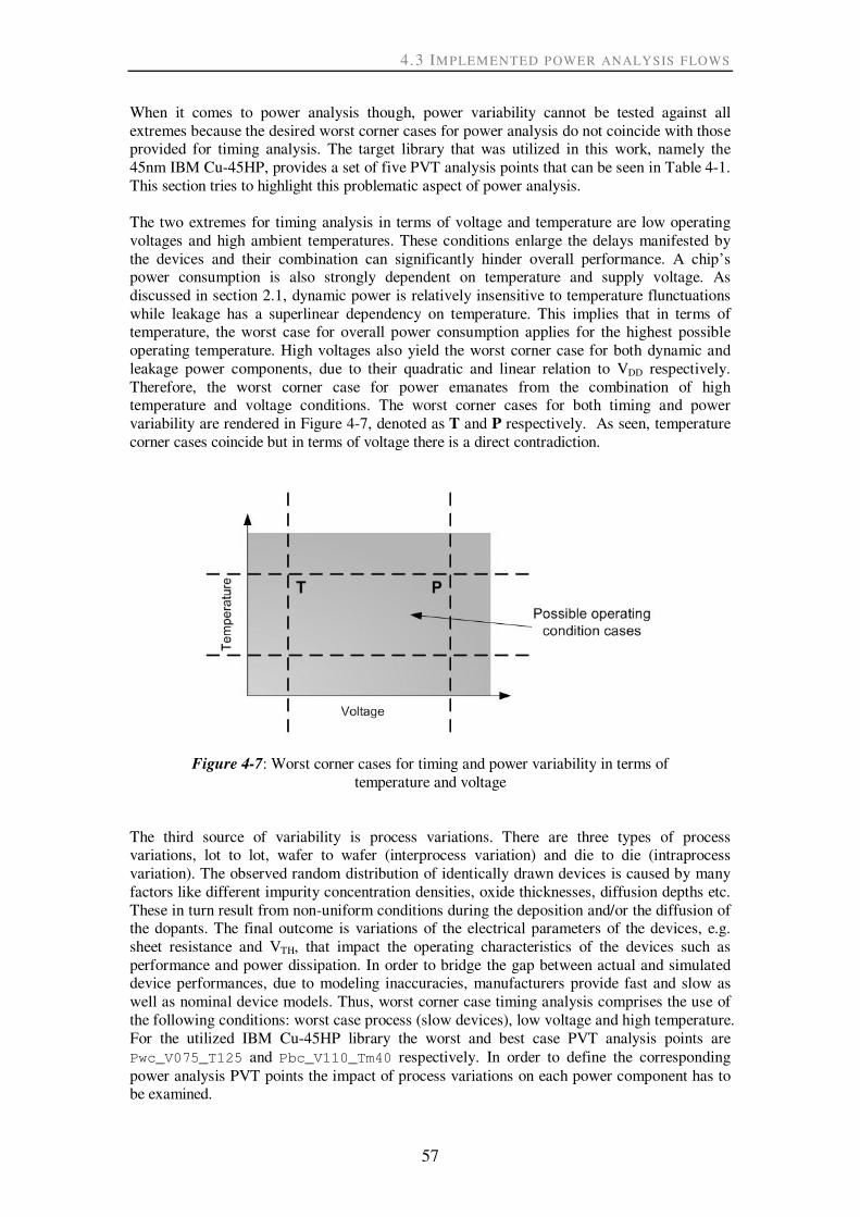
4.3 IMPLEMENTED POWER ANALYSIS FLOWS
57
When it comes to power analysis though, power variability cannot be tested against all extremes because the desired worst corner cases for power analysis do not coincide with those provided for timing analysis. The target library that was utilized in this work, namely the 45nm IBM Cu-45HP, provides a set of five PVT analysis points that can be seen in Table 4-1. This section tries to highlight this problematic aspect of power analysis. The two extremes for timing analysis in terms of voltage and temperature are low operating voltages and high ambient temperatures. These conditions enlarge the delays manifested by the devices and their combination can significantly hinder overall performance. A chip’s power consumption is also strongly dependent on temperature and supply voltage. As discussed in section 2.1, dynamic power is relatively insensitive to temperature flunctuations while leakage has a superlinear dependency on temperature. This implies that in terms of temperature, the worst case for overall power consumption applies for the highest possible operating temperature. High voltages also yield the worst corner case for both dynamic and leakage power components, due to their quadratic and linear relation to VDD respectively. Therefore, the worst corner case for power emanates from the combination of high temperature and voltage conditions. The worst corner cases for both timing and power variability are rendered in Figure 4-7, denoted as T and P respectively. As seen, temperature corner cases coincide but in terms of voltage there is a direct contradiction.
Figure 4-7: Worst corner cases for timing and power variability in terms of
temperature and voltage The third source of variability is process variations. There are three types of process variations, lot to lot, wafer to wafer (interprocess variation) and die to die (intraprocess variation). The observed random distribution of identically drawn devices is caused by many factors like different impurity concentration densities, oxide thicknesses, diffusion depths etc. These in turn result from non-uniform conditions during the deposition and/or the diffusion of the dopants. The final outcome is variations of the electrical parameters of the devices, e.g. sheet resistance and VTH, that impact the operating characteristics of the devices such as performance and power dissipation. In order to bridge the gap between actual and simulated device performances, due to modeling inaccuracies, manufacturers provide fast and slow as well as nominal device models. Thus, worst corner case timing analysis comprises the use of the following conditions: worst case process (slow devices), low voltage and high temperature. For the utilized IBM Cu-45HP library the worst and best case PVT analysis points are Pwc_V075_T125 and Pbc_V110_Tm40 respectively. In order to define the corresponding power analysis PVT points the impact of process variations on each power component has to be examined.

CHAPTE R 4 POWER ANALYSIS FLOWS
58
Figure 4-8: Qualitative illustration of PDYN and PLEAK dependency on process [8] As discussed in section 2.1.1, dynamic power is described by PDYN = αCLVDD
2f. It is obvious that only CL, which is a combination of wire and device capacitances, is affected by process variations. Fast device models exhibit smaller parasitic capacitances and thus smaller dynamic power dissipation, given that all other factors remain constant. Hence, due to the linear relation of CL to PDYN process dependency is weak [8]. Conversely, when it comes to leakage power there is a strong process dependency due to the fact that leakage power is dominated by subthreshold leakage, which increases exponentially with VTH. Threshold voltages in turn vary a lot with process due to changes in oxide thickness, substrate, polysilicon and implant impurity levels, etc. Consequently, fast device models that exhibit lower voltage thresholds suffer more from leakage power dissipation. In other words, due to the leakage being exponential in VTH, excessive VTH scatter can cause severe overall power increase [8, 9]. The dependencies of dynamic and leakage power on process variations are rendered in Figure 4-8 in a qualitative way. As can be seen, the manufacturing window is constrained by both timing and power limits. Summing up, it becomes clear that the worst case PVT point for power analysis, which comprises the conditions of best case process, high voltage and high temperature, does not coincide with the corresponding PVT point for timing analysis. The IBM Cu-45HP library doesn’t provide the desired PVT point as well. Therefore, in order to determine the corner cases for power, given the performance-oriented set of PVT points, the available operating conditions have to be swept and corresponding results compared. The results of this simple technique are presented in Chapter 6.
4.4 Power analysis script In order to perform the previously discussed power analyses and generate the desired reports, a generic power analysis script had to be implemented for use with PrimeTime PX. This section provides information on the implementation and explains the functionality of the script. Before digging into any details, a few things need to be said about the file requirements for performing an averaged power analysis. First of all, apart from a valid PrimeTime PX license, a setup file (.synopsys_pt.setup) is required so as to initialize the tool’s environment,

4.4 POWER ANALYSIS SCRIPT
59
e.g. environmental variables, references, etc. Moreover, in order to complete the analysis the following files need to be prepared in advance [3]:
� Gate-level netlist of the design under analysis. PrimeTime PX supports gate-level netlists only. Netlists contains leaf-level cells that are the instantiation of the library cells. Acceptable formats are Verilog, VHDL, EDIF, db, ddc, or Milkyway.
� Technology library files (.db) that contain library cells. Each cell has timing, power, and characterization information. As discussed, internal and leakage power are in the libraries.
� Synopsys Design Constraints file (SDC) that contains the design’s constraints. The driver cell information is used to calculate the transition time on the primary inputs.
� Switching Activity files. In the averaged power analysis, both SAIF and VCD file formats are acceptable to read in the switching activity.
� Parasitics annotation file (usually SPEF). This file is acquired after layout and if not available, wire load models are used instead for modeling capacitances of the nets.
� TCL script. In general, a TCL script containing all the needed commands and directions for PrimeTime PX needs to be sourced.
4.4.1 analyzeAveragePower – TCL script wrapper With the intention to enhance the realized power analysis script and make its use generic and transparent to the user, the whole implementation was split into two files. The first one, which is a tcsh14 script file called analyzeAveragePower, is presented in this section and serves as a wrapper/interface to the second PrimeTime PX TCL script file. By using analyzeAveragePower it is possible to run a user-customized average power analysis on a certain design netlist, as long as the above file list is prepared a priori. The script requires from the user to provide a set of switches that describe the desired type of analysis and other secondary information. Some default settings are always assumed, e.g. pre-layout analysis, operating conditions, analysis directory path, etc., but the user always has to provide an essential input like the netlist’s filename. It supports all types of power analysis presented in this chapter, namely RTL, pre-layout and post-layout gate-level analysis. The functionality of the script, which is represented in the flowchart of Figure 4-9, can be described as a set of consecutive steps. Firstly, the script sets the required analysis parameters assuming some default values. Then, the user’s command-line directives are captured and the analysis parameters are correspondingly updated. Subsequently, a check is performed for possible parameter discrepancies or missing files and the selected analysis settings are reported back. Next, the required, unique for each analysis, sub-directories are created and parameters are aggregated into a single pass variable. Finally, PrimeTime PX is invoked along with passing the user’s parameters. After the analysis is finished, control returns again to the script for redirecting the user to the generated reports before ending the process. The interface of the script, in terms of user-defined parameters, is provided in Appendix B, Table B-1. As an example, an input command for running a simple pre-layout gate-level power analysis would look like this: analyzeAveragePower -netlist_name <netlist_name> -saif_name
<saif_name> -top_entity <design_top_instance> -saif_strip_path
<saif_top_instance> -clock_tree_buffer <ct_estimation_buffer>
14 Tcsh is an enhanced, but completely compatible version of the Berkeley UNIX C Shell (csh).

CHAPTE R 4 POWER ANALYSIS FLOWS
60
Set analysis parameters and assume default values
Capture user’s command -line analysis parameter values
Check for discrepancies /missing files and report analysis settings
Create report directories
Invoke PT-PX and pass user
parameters to the TCL script
Figure 4-9: Flowchart of the analyzeAveragePower tcsh script 4.4.2 PrimeTime PX power estimation TCL script The second file, called estimate_average_power.tcl, is a TCL script file that comprises the set of commands needed by PrimeTime PX to perform a power analysis according to the user’s specifications. It is a generic script for average power estimation, based on the flow recommended by Synopsys in [3], automatically sourced to the tool by the analyzeAveragePower script. The commands in the script are grouped into different sections, which represent the basic steps of power analysis. This set of eight consecutive steps, more or less common for all types of power analysis, is shown in the flowchart of Figure 4-10. The first step enables PrimeTime PX, which provides power analysis, by setting the power_enable_analysis variable to TRUE. By default PrimeTime PX is disabled. In the second step, the desired analysis mode for power calculation is selected by setting the power_analysis_mode variable. Three different analysis modes are provided: averaged, time_based and leakage_variation. This script was written for averaged power analysis but it can easily support all modes due to common flow steps. The third step involves reading in the design’s netlist, constraints and parasitics annotation and of course defining the library and search paths before linking. Step four defines the operating conditions (or environmental characteristics, i.e. process, temperature, voltage, interconnect model) under which the current design is to be analyzed, by invoking the set_operating_conditions command. Next, step five is about annotating the switching activity, i.e. toggle_rate and static_probability attributes, for nets, ports, and pins of the current design by invoking the read_saif command. As discussed, this information is needed to calculate dynamic power values. If a RTL power analysis is performed then the name-mapping file, see section 4.3.1, should also be sourced at this step before read_saif. In the sixth step options for the selected power analysis mode are selected, by invoking the set_power_analysis_options command. Some options may be used for one or more modes of power analysis.

4.4 POWER ANALYSIS SCRIPT
61
In the seventh step the actual power estimation takes place. In case of a RTL or pre-layout analysis, for which a clock network isn’t synthesized in the netlist, the tool provides the estimate_clock_network_power command that virtually generates a clock tree for each clock and calculates its corresponding power. The clock trees are built on the fly and the original design is not touched or modified. Power information is calculated and updated on the design by invoking the update_power command. Update_power explicitly prepares the design for further analysis since power is also automatically updated by any other command that retrieves power results. Finally, in the eighth step power reports are generated by invoking the report_power command. Report_power accepts a plethora of arguments and sorting/filtering options that can in turn yield highly customizable power reports. The script in general produces many reports for keeping a good overview of the design, which are discussed in the next section.
Enable power analysis
Select power analysis mode
Read design data, parasitics and constraints . Setup libraries and
link design .
Specify operating conditions
Read in switching activity data and name-mapping commands
Specify options for the selected power analysis mode
Perform power analysis
Generate power reports
Figure 4-10: Flowchart of the estimate_average_power.tcl script 4.4.3 Power debugging features A visual, user-controlled approach to power debugging is a necessity for designers for verifying their power goals, thus minimizing power consumption. PrimeTime PX can generate a wide range of reports that provide information about a design and its power consumption. Moreover a graphical user interface can be invoked, which provides a way to

CHAPTE R 4 POWER ANALYSIS FLOWS
62
view design data and analysis results in graphical form. This section briefly discusses the reports that are generated by the estimate_average_power.tcl script. Most of the steps comprising the script’s flowchart generate one or more reports, depending on each step’s context and power analysis type. The first report, invoked by the report_annotated_parasitics command, is generated for post-layout gate-level analysis and reports net parasitics back-annotation on the current design. Additionally, the –check argument was used so as to report nets with incomplete parasitics as well (such nets with partially annotated parasitics were completed by inserting capacitances and resistances derived from the library’s wire load model). The next two reports, common for all analysis types, display attributes, i.e. operating conditions, wire load models, design rules, etc., and timing information for the current design. They are invoked by the report_design and report_timing commands respectively. In case of a RTL analysis, the report_name_mapping command reports the user-defined name mapping rules, which have been created by the set_rtl_to_gate_name commands that comprise the name-mapping file already sourced in PrimeTime PX. It is of importance to have an overview of the switching activities on the nets, therefore a subset of three reports is created for this reason by invoking the report_switching_activity command along with the appropriate arguments. By calling the command combined with the -average_activity, -hierarchy and -base_clock flags, average switching activity is computed for each subblock in the design and averaged toggle rates over the nets with respect to the period of the clock in the design are reported. The reported values are very useful because they indicate how active the design and its subcomponents are. Moreover, by using the -coverage flag a summary report is produced about the nets that have switching activity information, but few toggles. This report can be used to verify that switching activities from simulation or propagation are properly exercising the design. It can also be checked whether each block in the design is properly exercised by adding the -hierarchy flag. A report that reviews design nets that have no user switching activity annotation is also created, by using the command with the -list_not_annotated flag. Before generating the final reports it useful to invoke the check_power command, which checks the structure of the design for potential power violations. This command is used to identify possible power calculation problems before updating power. Finally, calling the report_power command generates the power reports for the design or a specific hierarchy. The type of power report generated is called a summary power report and displays internal, leakage, switching and total power values. The summary power report also reports power for various default or user-defined power groups like combinational, sequential, I/O pads etc. It should be noted that for RTL and pre-layout gate-level analysis the command is used along with the -include_estimated_clock_network argument, which indicates that the clock network (CT) power, estimated by estimate_clock_network_power, is to be included in the power report. For post-layout analysis the clock network is already synthesized in the netlist. The commands discussed in this section are summarized in Table 4-2, classified according to power analysis type. More information on commands and variables can be found in [10] and [11] respectively. Apart from the above mentioned reports, designers can also invoke PrimeTime PX GUI in order to acquire a high-level overview of the design’s power consumption. This visual analysis tool can be utilized after the design has been read, linked, and its power calculated. The GUI helps in the direction of visualizing and understanding the nature of power problems in the design, including the type, number, magnitude, and locations of the problems in the hierarchy. This is achieved by providing special visually enhanced analyses such as treemaps, histograms, schematic and waveform viewers, cell data tables etc. As an example, Figure 4-11 illustrates a treemap for the total power density of the examined Asterix design, in which the

4.4 POWER ANALYSIS SCRIPT
63
area of each node represents its corresponding relative total power within the design. Treemaps convey hierarchical data with squares that represent cells in the hierarchy.
TABLE 4-2 SUMMARY OF THE EMPLOYED REPORT GENERATING COMMANDS
RTL analysis Pre-layout Gate-level
analysis Post-layout Gate-level
analysis
report_design report_design report_annotated_parasitics
report_timing report_timing report_design
report_name_mapping report_switching_activity report_timing
report_switching_activity check_power report_switching_activity
check_power report_power (including CT) check_power
report_power (including CT) report_power
Figure 4-11: Treemap for total power density of Asterix design. The color gradient indicates increasing power consumption.
In chapter four the implemented power analysis flows and scripts have been presented along with some background information on power modeling and calculation. Moreover, the correlation between worst corner case timing and power analysis has been discussed. Chapter five covers the implemented power optimization flow and the corresponding integrated power reduction techniques.

CHAPTE R 4 POWER ANALYSIS FLOWS
64
4.5 References [1] Synopsys Power CompilerTM User Guide, Version B-2008.09-SP2, December 2008.
[2] Switching Activity Interchange Format (SAIF), “Synopsys Inc.”, Technical Report, 2002.
[3] Synopsys PrimeTime® PX User Guide, Version B-2008.12, December 2008.
[4] “Synopsys PrimeTime PX Power Analysis Solution Achieves Broad Market Adoption”,
EDACafe, May 2009, last accessed 15.06.2009,
http://www10.edacafe.com/nbc/articles/view_article.php?section=CorpNews&articleid=694271
[5] Synopsys Synthesis Commands, Version B-2008.09, September 2008.
[6] Wikipedia, Standard Parasitic Exchange Format article, last accessed 20.06.2009,
http://en.wikipedia.org/wiki/Standard_Parasitic_Exchange_Format
[7] S. R. Nassif, “Modeling and analysis of manufacturing variations”, In Proc. of Asia and
South Pacific Design Automation Conference, May 2001.
[8] S. R. Nassif, “The impact of variability on power”, ppt slides, UT VLSI Seminar Series,
March 2006, http://www.cerc.utexas.edu/vlsi-seminar/spring06/slides/2006.03.03.srn.pdf, last
accessed 03.07.2009.
[9] Richard Goering, “Hope seen for taming IC process variability at next design node”,
EETimes article, April 2006, last accessed 27.06.2009, http://www.eetimes.com/news/
latest/showArticle.jhtml?articleID=185302775
[10] Synopsys PrimeTime Suite Commands, Version B-2008.12, December 2008.
[11] Synopsys PrimeTime Suite Variables, Version B-2008.12, December 2008.

65
55
PPoowweerr OOppttiimmiizzaattiioonn FFllooww This chapter discusses the implemented power optimization flow, using Synopsys tools. The incorporated power reduction techniques are again briefly revisited, providing additional information on how these techniques are approached and supported by Synopsys. Furthermore, the tools and respective commands are introduced.
5.1 Integrated power reduction techniques So far, a broad range of power-saving techniques has been presented that covers both the transient and static components of power dissipation. In particular, chapter three shortly discussed a total of twenty-one techniques that can be applied at various levels of abstraction. The attainable power savings were extracted from the literature in a qualitative manner, as well. In order to accurately evaluate and measure the effectiveness of the power reduction techniques, a subset of the aforementioned techniques was selected for this purpose. The criteria for formulating this subset were mainly four: tool support, level of application, verification capabilities and effort. Most of the ASIC EDA tools provide some automatic methods for performing power optimization. The same applies for the Synopsys tools that were used in this work; therefore the selected techniques fall within the set of Synopsys PowerCompilerTM supported power optimization techniques. Moreover, due to the fact that the examined target design is an ASIC block of industrial complexity, the techniques ought to be

CHAPTE R 5 POWER OPTIMIZATION FLOW
66
applicable at the RT and/or gate level. Techniques that require decisions to be taken at earlier design stages would necessitate the knowledge/modification of the internal architecture of the block, which is out of the scope of this Thesis, therefore they were left out. Other techniques that introduce power states would need corresponding verification scenarios that did not exist at the time, so they were left out as well. The effort required for each power technique’s implementation was also taken into account due to the limited timeframe of this work. The tool that was used for the realization of the power optimization flow is PowerCompiler, which is part of Synopsys's DesignCompiler synthesis family. It offers power analysis and optimization technology from RTL to the gate level. PowerCompiler supports the following power reduction techniques: clock gating, operand isolation, MTCMOS, multi-voltage and multi-supply designs and power gating (also referred to as power switching). Based on the above criteria, the techniques that comprise the subset integrated into our optimization flow are the following:
� Clock Gating (RTL and gate-level PDYN reduction) � Operand Isolation (RTL PDYN reduction) � Gate-Level power optimizations (gate-level PLEAK and further PDYN reduction)
Additionally, fixed usage of low-power operators and the selection of power-driven clock gating are also introduced as options in the flow. These techniques can achieve power savings in the front-end synthesis domain. The following subsections briefly revisit the principles of the above power reduction techniques, focusing on how they are supported and performed by the tool. 5.1.1 Clock Gating With the capability of clock gating, PowerCompiler can implement circuits in a different way compared to DesignCompiler. DesignCompiler implements load enable registers by use of feedback loops. However, these registers maintain the same logic value through multiple cycles and unnecessarily waste power. Figure 5-1 shows a simple load enable register bank implementation in DesignCompiler. Clock gating is actually an alternative implementation of load enable registers that saves power by eliminating the unnecessary activity associated with reloading register banks. Before gating the clock signal of a register though, PowerCompiler checks if certain conditions are satisfied. First, the register must be a load enable flip-flop. An example of such a register in matching HDL code is the following:
@posedge (CLK)
begin
if (EN == 1)
Q = DATA_IN;
end
end
Second, the register should belong to a bank with a bitwidth equal to or larger than a value specified by the designer. Because a clock gating circuitry is implemented for each register bank, a register bank should have a reasonable size to be considered for clock gating. This is also library dependent. It is also required that the enable signal of the register bank be synchronous with its clock, for latch-free clock gating. This is the setup condition. For latch-based or integrated clock gating, PowerCompiler can insert clock gating irrespective of the enable signal’s and the clock’s clock domains. Clock gating can be implemented as simply as by inserting a two-input gate in the clock net of the register. This is called a latch-free implementation and is prone to glitches, which

5.1 INTEGRATED POWER REDUCTION TECHNIQUES
67
should be avoided under all circumstances. A safer, but larger, implementation is the one involving a latched clock-enable signal in order to avoid transitions while the clock signal is high and there are glitches on the control logic output. This implementation is called latch-based clock gating. A side effect of gating a register’s clock is that it makes it uncontrollable for test (unless there is a dedicated scan clock). PowerCompiler can add control points to increase the testability of the design by restoring the clock signal to its non-gated form during test. Each control point is a scan enable signal implemented using an OR gate that eliminates the function of the clock gate during test, which restores the controllability of the clock signal. This kind of test solution has fault coverage comparable to that of a design without gating clock. Figure 5-2 depicts a latch-based clock gating implementation using a two-input AND gate, that also includes an inserted SCAN_ENABLE signal as test control point to improve testability.
DFFControl
Logic
0
1
Register
Bank
D Q
CLKEN
DATA_IN
DATA_OUT
Figure 5-1: DesignCompiler implementation of a synchronous load enable register bank using a feedback loop and a multiplexer.
DFFControl Logic EN
Latch
LD
LG
LQ
ENL
CLK
Register
Bank
D QDATA_OUT
EN_CLK
SCAN_ENABLEDATA_IN
Figure 5-2: PowerCompiler latch-based clock gating implementation of a synchronous load enable register bank with improved testability.
PowerCompiler is able to insert clock gating circuitry either into RTL designs or in post-synthesis gate-level netlists. In case of a gate-level netlist the design is re-synthesized with clock gating logic. Insertion of clock gating can be done by compiling the design using the -gate_clock option of the compile or compile_ultra command. Alternatively, one can also insert clock gates to a GTECH netlist using the insert_clock_gating command. During the compilation process clock gates are inserted on the qualified registers, with the cost factor considered being design topology. During the clock gate insertion the compile_ultra command uses the default values of the set_clock_gating_style command and also honors the setup, hold, and other constraints specified in the technology libraries. These values can be overridden by calling the same command with the desired

CHAPTE R 5 POWER OPTIMIZATION FLOW
68
arguments before compiling the design. PowerCompiler also provides the ability to perform clock gating on DesignWare components instead of treating them as black box cells. The compile_ultra -gate_clock command performs clock gating on DesignWare components, by default. In case the insert_clock_gating command is used, then the power_cg_designware variable has to be set to true. Furthermore, PowerCompiler supports power-driven clock gating. This new feature is enabled by setting the power_driven_clock_gating variable to true before compiling, using the compile_ultra -gate_clock command. Power-driven clock gating performs clock gate insertion, optimization, and removal considering the cost factor of dynamic power and switching activity. The underlying algorithm examines all register banks that can potentially be clock gated, calculates their power with and without clock gates, and retains the clock gates that provide lower power costs. The set_clock_gating_style command is still honored, however using the -min_bitwidth option with this algorithm is not recommended. The effectiveness of the algorithm is examined in this work. 5.1.2 Operand Isolation Operand isolation reduces power consumption by suppressing redundant computations in combinational circuits. PowerCompiler performs power-based, automatic, RTL exploration and insertion of operand isolation. In order for the tool to apply the technique on a design object, all of the following criteria should be met: a) the object should be an arithmetic operator or a combinational hierarchical cell, b) the fanout of the object should have observable don’t care (ODC) conditions, and c) the aforementioned netlist exploration process should indicate that by inserting operand isolation the circuit’s dynamic power will most likely be reduced. Operand isolation does not take place unless the estimated reduction of total redundant toggles is enough to compensate for the toggles introduced by the isolation gates and nets. Due to this power-based exploration, operand isolation can be affected by static probabilities and toggle rates (i.e. switching activity) of the operator’s input data and of the nets that generate the control signals. Moreover, it also depends on the complexity of the isolation objects. The tool’s main methodology is to insert isolation logic and then decide on possible rollback15 action, after timing and power analysis. Two approaches are offered so as to incorporate operand isolation into a design flow. The first one, called the one-pass approach, entails only one compile step. Here, operand isolation insertion is performed during the mapping stage while rollback action takes place during timing optimization in the same compile. The second one, which is followed in this work, is called the two-pass approach and entails an initial compile followed by an incremental compile. This approach consists of two stages. Isolation logic is inserted during the first stage, followed by timing and power analysis. Rollback is possible to take place in the second stage. Basic utilization of operand isolation in PowerCompiler requires the following commands used and variables set. First of all, the do_operand_isolation variable has to be set to true, which essentially enables operand isolation (obviously having read in switching activity files should have been done in a previous step). Then, the operand isolation style used by PowerCompiler has to be set. This is done by the set_operand_isolation_style command, which specifies the isolation logic implementation and enables or disables user-driven operand isolation. By default, PowerCompiler automatically chooses which operands to isolate. If the -user_directives argument is used, only the operators and hierarchical combinational cells that were specified as potential candidates by the user are
15 Removal of the isolation logic, after the delay optimization, if the timing violation is not acceptable.

5.1 INTEGRATED POWER REDUCTION TECHNIQUES
69
considered. Regarding operand isolation removal, the set_operand_isolation
_slack command sets the timing threshold to a value below which the automatic isolation rollback operation is not triggered. It should be reminded that in a two-pass flow no automatic rollback is performed during the initial compile. The automatic isolation rollback mechanism takes place during a subsequent optimization step (compile –incremental). 5.1.3 Gate-Level Power Optimizations PowerCompiler approaches the gate-level power optimizations as additional steps to timing optimization. The tool takes advantage of positive timing slack to decrease a design’s dynamic and leakage power, without affecting its performance. Gate-level dynamic power optimization further reduces power after RTL clock gating and/or operand isolation. More importantly, leakage power optimization is performed on the non-critical paths (section 3.3.5). The positive slacks are used to swap low speed and low leakage power cells. As already discussed, slower cells allow higher threshold voltages, which can dramatically reduce leakage power. For this kind of optimization target libraries that are characterized for leakage power and contain cells with multiple threshold voltages are required. Single threshold voltage libraries are supported as well (optimization through cell resizing, section 3.3.6), however multithreshold voltage libraries can save much more leakage power. It should also be mentioned that because gate-level power optimization is performed together with other optimizations PowerCompiler calculates cost function components to weigh the relative benefit of potential optimization changes. These cost function components are evaluated independently in order of priority, as follows: design rule cost, max delay cost, min delay cost, max total power cost, max dynamic power cost, max static power cost, min porosity cost and max area cost. An optimization move is only accepted if it decreases the cost of one component without increasing the cost of a higher priority component. The required inputs for gate-level power optimization are RTL or gate-level netlist, power constraints, appropriate libraries and switching activity. Apparently, the output is an optimized gate-level netlist with the optimization being initiated with the compile or compile_ultra commands. Power constraints set the target power value for optimization. They are set by the set_max_leakage_power and set_max_dynamic_power commands, thus enabling leakage and dynamic power optimization respectively. A useful command for leakage optimization is the set_max_lvth_percentage. When the technology library has at least two voltage threshold groups for the library cells, the cells are grouped by the threshold voltage. This command can be used to control the percentage of the design’s cells that belong to the low voltage threshold group. For example, assuming that a design contains cells belonging to the lvt, xlvt, svt and hvt threshold groups, the following command specifies that lvt and xlvt are considered as belonging to the low threshold group that can take up as much as 15% of the total design area:
set_max_lvth_percentage -lvth_groups {xlvt lvt} 15
5.1.4 Low-Power Operators In DesignCompiler arithmetic operations, e.g. +,-,*, are implemented using the DesignWare library’s components. DesignWare is a library that consists of high-level functional modules that provides to designers the flexibility to infer them in HDL code. When reading in HDL code these predefined operations are automatically mapped to corresponding DesignWare operator implementations. The main advantages of using DesignWare components are resource sharing, selection of implementation based on design constraints, components optimization at higher design levels and shorter run times.

CHAPTE R 5 POWER OPTIMIZATION FLOW
70
Usually Designware components are multi-architecture components having at least two architectures; typically, one is designed for smallest area, and one is designed for maximum speed. This way, Synopsys tools have the flexibility to select the implementation that best meets the design constraints. Because power optimizations are not of the highest priority, the tool might prefer to use architectures that are known to be power hungry. In this case, based on the theoretical discussion of section 3.2.1, a designer might prefer to disable the selection of certain architectures, e.g. ripple-carry models. This can be done by the set_dont_use command. It should be noted that DesignCompiler’s versions past March 2007 do not support many of the architectures discussed in 3.2.1 for common operations, i.e. +,*, which have been substituted by the optimized parallel prefix architecture. In our case, a switch has been included in the synthesis script so as to exclude ripple-carry architectures from the synthetic libraries. The purpose of the above text, which is largely taken from manuals, is to make the next section standalone and easier to understand without having to refer to tool guides. However, the above do not substitute Synopsys’ literature and the interested reader should refer to [1] and [2] for more details.
5.2 Power optimization flow description PowerCompiler always works within DesignCompiler’s shell and is therefore transparent to DesignCompiler’s users. This feature allows the integration of the abovementioned power reduction techniques into a typical synthesis script. This section describes the implemented power optimization flow in terms of optimization steps and corresponding commands. The flow, which actually comprises two main phases with intermediate steps, can be seen in Figure 5-3. The main concept of the flow is to allow power optimizations during the first phase and then try to further reduce power in the gate-level netlist of the second phase, by providing better annotation, low power library cells and power-driven clock gating. The flow’s starting point is naturally a set of synthesizable RTL VHDL models. As with the power analysis flows, the first step is about simulating the VHDL code, in order to obtain the required switching activity information and to verify the models. Usage of Cadence’s NC-Sim simulator is involved in this step. The output of the first step is a backward RTL SAIF annotation file that is used later on by PowerCompiler. Before reading in the RTL source files, the saif_map –start command is used to facilitate the name mapping mechanism. The second step involves elaboration and synthesis. After the GTECH netlist generation, certain parameters have to be setup before the first compilation. The used technology library, the 45nm IBM Cu-45HP, is a multi-threshold library that provides cells with three available voltage thresholds, namely the hvt, svt and uvt. The hvt cells, which have a low VTH and are the fastest, are usually only used during physical synthesis for timing closure. On the contrary, the uvt cells have a high VTH and therefore exhibit the least leakage and speed. Svt cells are the “normal”, in-between case, compromising both leakage and speed. During the first phase the tool is constrained to use only svt cells. Next, clock gating style is set: set_clock_gating_style -positive_edge_logic {integrated} \
-control_point before \
-minimum_bitwidth 8 \
-max_fanout 2048 \
-control_signal scan_enable -setup 0.3

5.2 POWER OPTIMIZATION FLOW DESCRIPTION
71
Figure 5-3: The implemented power optimization flow

CHAPTE R 5 POWER OPTIMIZATION FLOW
72
The following commands are used for performing clock gating insertion and DesignWare components clock gating. It is evident that the first phase’s clock gating cost factor considered is design topology, -minimum_bitwidth, and not estimated power.
set power_cg_designware TRUE
insert_clock_gating -global Performs clock gating on an appropriately-prepared GTECH netlist on all subdesigns as one
global step (original design should be uniquified).
The following commands enable operand isolation. This technique is inherently power-driven, therefore switching activity has to be annotated before compilation. In this case the name mapping mechanism has to be used as well.
read_saif -input <RTL_saif> -instance <> -auto_map_names
Specifies that a name mapping will be created automatically using SAIF file,
and the created name mapping will be used to read the SAIF file.
set do_operand_isolation TRUE
set_operand_isolation_style -logic adaptive –verbose The adaptive value allows the tool to determine whether AND- (isolate to 0) or OR-logic (isolation
to 1) is the optimal implementation.
set_operand_isolation_slack 0.15 -weight 0
Automatic rollback is performed during the second compile (weight set to 0 causes this).
Next, dynamic and leakage power optimizations are enabled by the subsequent commands. The target values for both dynamic and leakage power are set to zero, so as to indirectly infer the algorithm’s maximum effort. Additionally, the svt cells are specified as belonging to the low VTH group, which is allowed to take up the whole of the circuit’s area.
set_max_leakage_power 0
set_max_lvth_percentage 100 -lvth_groups {sc_12t_svt}
set_max_dynamic_power 0 Concluding the power constraints for phase one, ripple-carry architectures can be excluded from the synthetic libraries with the purpose of constraining the tool to use only optimized architectures during mapping.
set_dont_use standard.sldb/DW*/rpl
set_dont_use dw_foundation.sldb/DW*/rpl
The output of the first phase is an intermediate gate-level netlist, which is accordingly power optimized. This netlist is the starting point of the second synthesis phase. The first step of this phase involves again simulating the gate-level netlist using the NC-Sim simulator. This step is the same as previously described but it takes much longer to complete. The produced SAIF annotation is complete though. Incremental compilation comprises the second step, after certain alterations in the technology library and clock gating style. As discussed in 5.1.3 leakage power optimization takes advantage of positive timing slack to decrease a design’s static power, without affecting its performance. Assuming that our target frequency is within a feasible range, which is actually true in this work since we constrained the design to 250MHz, then after the first phase the design has “stocked” positive slack due to using only the relatively fast svt cells. In the second phase we add the uvt cells library in the

5.2 POWER OPTIMIZATION FLOW DESCRIPTION
73
target library as well, in order to allow for the tool to tradeoff the slack with leakage power. At the same time we constrain PowerCompiler to use svt cells only for a minimum percentage of the design’s area, thus straining the optimization margins.
read_saif -input <gate-level_saif> -instance <>
No name mapping needed for gate-level annotation.
set_max_leakage_power 0
set_max_lvth_percentage 2 -lvth_groups {sc_12t_svt} Svt cells are constrained to a minimum of 2% (this percentage depends on the amount
of positive slack).
set_max_dynamic_power 0
Regarding clock gating, its power-driven feature is enabled and extra optimizations are introduced, namely multistage and hierarchical clock gating. Multistage clock gating allows combining as many register banks as possible so that the clock gating can be moved up closer to the root, resulting in more power savings. Moreover, the tool can balance the number of clock gating stages across various register banks so as to ensure uniform clock latency. Hierarchical clock gating looks for globally shared enables across registers in different levels of hierarchy while inserting clock gating cells, thus increasing the gating opportunity. The following commands allow for a fully optimized clock gating insertion: set_clock_gating_style -positive_edge_logic {integrated} \
-control_point before -num_stages 6 \
-max_fanout 2048 -control_signal scan_enable -setup 0.3 The -num_stages argument specifies the maximum number of stages for multistage clock
gating. Also note that the -min_bitwidth option has been removed for power-driven clock
gating.
set power_cg_balance_stages TRUE
set compile_clock_gating_through_hierarchy TRUE
set power_driven_clock_gating TRUE
compile_ultra -incremental -gate_clock
Runs a high effort compile in incremental mode, which does not run mapping
or implementation selection stages (faster).
Finally, the output of the described flow is a pre-layout power optimized tech-mapped netlist. It should be noted that all of the above mentioned power optimization techniques can be enabled or disabled independently, thus they can also be evaluated independently, by setting/unsetting the corresponding synthesis script switches. Chapter five has presented the implemented power optimization flow along with its incorporated power reduction techniques. PowerCompiler’s approach to these techniques and respective commands have also been discussed. In chapter six the evaluated power savings’ results and flow comparisons are presented.

CHAPTE R 5 POWER OPTIMIZATION FLOW
74
5.3 References [1] Synopsys PowerCompilerTM User Guide, Version B-2008.09-SP2, December 2008.
[2] Synopsys Synthesis Commands, Version B-2008.09, September 2008.

75
66
RReessuullttss aanndd CCoommppaarriissoonnss Chapter six provides a quantitative evaluation of the flows implemented in this work, based on a large industrial example design. The power analysis flows are compared in terms of accuracy and runtime and the estimated impact of power optimizations is presented. Worst corner case power analysis results are also illustrated along with a brief introduction to the example design used.
6.1 The employed target design In order to evaluate the implemented flows a target design had to be employed. The main criteria that had to be satisfied were the design’s size, to allow for synthesis/optimization/ analysis iterations within reasonable time frames, and of course something being of interest to Ericsson. The selected design, named after Asterix, is an Ericsson’s custom-made FFT accelerator with a main task of switching fast between the time and frequency domains. Asterix is a common ASIC block that is largely used and continuously improved by Ericsson. In turn, it contains a smaller sub-block named after Idefix, which is the core calculation unit. Idefix exhibits a large amount of switching activity as long as it has data to perform on. It should be added that Asterix’s testbench used during simulations has been written with a main purpose of proving the block’s functionality over a large set of operating parameters, keeping it continuously busy with jobs. In other words, the used testbench has been designed for

CHAPTE R 6 RESULTS AND COMPARISONS
76
verification purposes only rather than for power analysis. All of the results/comparisons that are presented subsequently refer to Asterix.
6.2 Power analysis flows comparison Chapter 4 highlighted the importance of power regression test methodology, which in turn entailed the key role of the power analysis flows’ characteristics. In this thesis work three power analysis flows have been realized, namely the RTL, pre-layout gate-level and post-layout gate-level, and their traits and differences have been discussed. This section compares and contrasts the three flows, in terms of runtime and attainable accuracy. Moreover, the PVT analysis points, provided by the IBM CU-45HP library, are examined and the worst corner case for power analysis is identified. The following essentially help circumscribe the answers for the questions set in section 4.3. 6.2.1 Power analysis accuracy Figure 6-1 illustrates the estimated averaged power dissipation of Asterix, after each of the three realized analysis flows is applied to the design. In order to put emphasis on the contribution of each of the power components to the total consumption, a stacked column chart was utilized. All columns are analyzed into cell leakage power, net switching power and cell internal power. The first column identifies the RTL analysis flow, the second the pre-layout gate-level and the third column the post-layout gate-level. The vertical axis corresponds to the absolute values of power, in mW, though useful findings are extracted from a comparative evaluation. In addition, next to each column an extra value is provided that allows for a correlation between user-annotated switching activity and accuracy.
Figure 6-1: Comparison of the realized analysis flows in terms of accuracy

6.2 POWER ANALYSIS FLOWS COMPARISON
77
Prior to commenting the above figure, it would be useful to go over the definitions of the power components. Leakage power is the power dissipated by a cell when it is inactive. Total leakage power of a design is computed by summing the leakage power values of all of the design’s library cells. Internal power is any power dissipated within the boundary of a cell and results from internal capacitances switching and short-circuit currents. Switching power results from the charging and discharging of the external capacitive load on the output of a cell, which is the sum of the net and gate capacitances on the driving output. It can be clearly seen from the comparison that, as expected, the RTL analysis flow exhibits the least accuracy, whereas the other two gate-level flows look closer to reality. This large difference principally stems from insufficient calculation of the switching power during RTL analysis, which in turn has to be credited to the inadequate switching activity annotation of the design’s objects. Cell internal power is affected by this inadequacy but to a lesser extent, owing to the cells mainly dissipating crowbar related power. Conversely, leakage power dissipation remains almost unchanged over the three flows, which straightforwardly indicates the direct relation of leakage to area and the usage of non-state dependent leakage models by the library. It should be reminded that both the RTL and pre-layout gate-level flows perform on the same netlist. The differences between the pre-layout and post-layout gate level flows might seem small but are quite important. Leakage power for the post-layout gate-level flow increases, as a result of the increase in the design’s area after the high-fanout nets synthesis (addition of buffers). The same applies for cell internal power. On the contrary, switching power is reduced for the post-layout gate-level flow on account of using annotated parasitics information, instead of relying on the overly pessimistic, for current tech nodes, wire-load models. 6.2.2 Power analysis runtime Apart from the attainable accuracy, the flows’ time requirements have also to be investigated. The three implemented analysis flows are evaluated by comparing the runtimes required for Asterix’s power analysis against each other. Figure 6-2 illustrates this contrast in terms of a stacked bar chart.
Figure 6-2: Comparison of the realized analysis flows in terms of runtime

CHAPTE R 6 RESULTS AND COMPARISONS
78
Each of the figure’s bars, identifying the respective power analysis flow, comprises three components, namely simulation, compilation and estimation time. These components more or less represent the critical steps of an analysis flow, as described in chapter four. The horizontal axis corresponds to each flow’s requisite time, in hours, to provide power estimations for Asterix. As can be seen, the RTL analysis flow requires the least amount of time for power estimation, whereas the other two gate-level flows are much more time consuming. The extra time required by the two flows is spent during the simulation step. This is attributable to the abstract RTL VHDL models that are fast to verify, where the other flows have to spend most of the time performing the simulation of technology-mapped detailed models. The same applies for the difference in simulation time between the two gate-level flows. Post-layout simulation time is larger because much more detail is included in the respective netlists, therefore their verification is calculus intensive. It can also be seen that the amount of time dedicated to compilation is the same for the RTL and pre-layout flows, and a small difference exists between the pre-layout and post-layout gate-level flows. This is due to the extra SoC Encounter sub-step required in the latter flow. RTL and pre-layout flows share the same synthesis steps but use different models during simulation. Finally, it should also be pointed out that the estimation time constitutes only a small percentage of the overall runtime. Naturally, as a design gets more complex this time increases but in an affordable manner, as inferred by Figure 6-2. 6.2.3 Worst corner case power analysis Continuing the discussion of section 4.3.4, we present Asterix’s power results after “sweeping” all the available operating conditions points provided by the IBM Cu-45HP library.
Figure 6-3: Available timing analysis PVT points and their respective power results

6.3 POWER OPTIMIZATION RESULTS
79
The results were extracted by simply iterating through all the offered PVT points during the power estimation step of the pre-layout gate-level flow. Although we know that this library does not provide the theoretical worst corner case power analysis point, such a practice is useful because it identifies the available worst case point and can indirectly show how much weight each power component has in the library’s power characterization. Figure 6-3 renders the correlation of the estimated power dissipation to the temperature and voltage conditions of each point, using a three-axis pivot chart. For visualization purposes the vertical axis power values form a surface that further highlights the correlation. Different shades show different power dissipation ranges, with black areas indicating the lack of the respective PVT points. As can be seen, the highest power values occur for the largest operating voltage and best-case process, i.e. for the Pbc_V110_Tm40 point (review table 4-1). This result shows the dominance of PDYN over PLEAK for the used library’s power characterization, and underlines the quadratic relation of PDYN to VDD. The identified worst corner case power analysis point doesn’t tally with the theoretical one, as expected, since voltage, temperature and process variation variables do not attain their worst case values simultaneously. It is interesting to note that the Pbc_V110_Tm40 point is also the one provided for best case timing analysis. It can also be seen that the Pnom_V0925_T085 point makes a good median point when it’s not required to qualify the design across extreme conditions. In any other case, due to the contradiction between worst corner case power and timing analysis points, some kind of analysis priority and acceptable uncertainty margins have to be decided based on design metrics. Figure 6-3 prescribes which point to use during analysis if power is the primary design metric.
6.3 Power optimization results The power reduction techniques incorporated into this work’s implemented power optimization flow have been discussed in chapter five. This section presents the estimated power results of the optimized Asterix, after applying the optimization flow. These results are the output of a pre-layout analysis flow for the Pwc_V090_T125 point. The impact of each technique on Asterix’s power dissipation, active area and performance is extracted and evaluated independently. Moreover, we focus on the power-driven feature of clock gating, comparing the results with and without its usage. 6.3.1 Impact on power dissipation Figure 6-4 illustrates the impact of the discussed power optimization techniques on Asterix’s power consumption. A stacked column chart was utilized so as to provide information on how each power component is affected. As with previous analyses, each column is analyzed into cell leakage power, net switching power and cell internal power. The first column identifies the unoptimized Asterix block. The second, third and fourth columns identify the optimized Asterix after gate-level power optimizations, clock gating and operand isolation respectively. Column five shows the design without ripple-carry operators while the final column identifies the combined impact of all the techniques on Asterix. The vertical axis corresponds to the estimated absolute power values in mW. Moreover, the value of each column’s power component is designated to allow for direct and exact comparisons.

CHAPTE R 6 RESULTS AND COMPARISONS
80
Figure 6-4: Impact of the applied power reduction techniques on power dissipation As can be seen from figure 6-4, clock gating provides the largest optimization benefits by reducing overall switching activity, thus reducing cell internal and net switching power. Furthermore, clock gating manages to indirectly reduce leakage power as well, by trimming down the design’s area for reasons that will be explained in section 6.3.2. Gate-level power optimizations have the second largest power-saving impact on the design. Naturally, leakage power is greatly improved by utilizing low VTH cells at the expense of a little more area. This happens because of the large percentage of uvt cells insertion that are more sizable. Net switching power is also slightly improved, however this gain is offset by the increase in area and the corresponding increase in cell-leakage power. The use of non-ripple-carry operators marginally improves dynamic power, however it is good to verify that such an option is on the positive side. Unfortunately, the operand isolation technique could not be evaluated, because the tool couldn’t find an opportunity to apply the technique on Asterix (criteria not met, see section 5.1.2). Finally, it can be seen that by combining all of the optimization techniques, a superposition of the impacts is achieved. Additionally, the negative side effects of leakage optimization seem to be partially offset. Quantitatively, in terms of percentages, our optimization flow manages to improve Asterix’s overall power consumption by 30%, while for leakage power alone the improvement is much larger reaching a 52.2%. 6.3.2 Impact on active area This section explains how the design’s active area is affected by the applied optimization techniques. Figure 6-5 illustrates the impact of each of the applied power optimization techniques on Asterix’s area, in a way analogous to figure 6-4. Each column identifies an optimization technique and the vertical axis corresponds to the absolute values of active area, in µm2. Because of the relatively small differences in area from column to column, a chart with broken Y-axis has been utilized so as to show up these differences.

6.3 POWER OPTIMIZATION RESULTS
81
Figure 6-5: Impact of the applied power reduction techniques on area As can be seen from figure 6-5, gate-level power optimizations cause a slight increase in the design’s area due to the mass insertion of uvt cells. What is more interesting though is the twofold improvement that clock gating offers to the design. As discussed in the previous section, apart from the reduction in switching activity clock gating also reduces area. Thanks to it being an alternative implementation to load enable registers, section 5.1.1, unnecessary activity is saved by replacing the multiplexers and feedback loops with clock gating logic. Apparently the latter requires less area, thus meriting the technique. The rest of the techniques do not affect Asterix’s area. It is also seen that by combining all of the optimization techniques, a superposition of the impacts is achieved in terms of area. Summing up, there is an impact of power optimization on area, which is not significant but notable, around 4%, owning to the aforementioned “positive side effects” of clock gating. 6.3.3 Impact on performance This section examines the impact of power optimization on the design’s performance. Figure 6-6 shows the impact of each of the applied power optimization techniques on Asterix’s performance. Performance is evaluated in terms of maximum attainable frequency. The chart’s vertical axis corresponds to the absolute values of clock frequency, in MHz. For this work Asterix was synthesized with a maximum frequency constraint of 250 MHz, though the design is able to operate at much higher frequencies. As can be seen from figure 6-6, the unoptimized Asterix has a large amount of positive slack, owning to the exclusive utilization of the relatively fast but leaky svt cells. This translates into a plethora of non-critical paths. It is also seen that performance is only affected by the gate-level power optimization techniques, in particular by leakage optimization. Thus, the second column, which identifies this technique, illustrates in the best way the tradeoff between positive slacks and leakage power reduction16. Apparently, overconstraining a design in terms of performance reduces the number of non-critical paths, thus shrinking the available optimization margins.
16 You may need to review sections 3.3.5 and 5.1.3.

CHAPTE R 6 RESULTS AND COMPARISONS
82
Figure 6-6: Impact of the applied power reduction techniques on performance 6.3.4 Power-driven clock gating As discussed in section 5.1.1, power-driven clock gating considers the switching activity when it comes to gating load enable registers. On the contrary, when this feature is disabled, typical clock gating is applied on a design topology basis honoring the constraints and parameters set by the user. One important parameter is the minimum bitwidth, which specifies the minimum size of a register bank for which the clock can be gated. This section evaluates the effectiveness power-driven clock gating in further reducing power consumption. Figure 6-7 compares the attainable power savings with and without enabling power-driven clock gating. The figure’s first column identifies power-driven clock gating and the second column identifies the topology-based, typical clock gating. Each column is analyzed into the basic power components, with the vertical axis corresponding to the estimated absolute power values, in mW. Apart from the exhibited power values, additional information is provided regarding the percentage of gated registers and the design’s respective active area, for each of the two clock gating modes examined. As can be seen, typical clock gating gates 91% of the design’s registers, resulting in an active area of 188011 µm2. On the other hand, power-driven clock gating, which utilizes gate-level switching activity annotation, gates 65% of Asterix’s registers. Apparently the remaining load enable registers were not active enough so as to insert clock gating logic. Different insertion rates, stemming from different underlying clock gating algorithms, result in different active areas. Although area directly affects leakage and cell internal power, the side effects of clock gating do not seem to be taken into account. Hence, typical clock gating achieves better power results owning to the larger degree of logic optimization (multiplexer and feedback loops removal). This phenomenon appeared quite odd, since power-driven clock gating is much advertised by the PowerCompiler’s manual. Indeed, after Synopsys was contacted for this issue, technical personnel confirmed that the underlying power-driven algorithm doesn’t take all the parameters into account, therefore yielding worse results. It is expected that the algorithm will be improved in the next tool versions. At this point it should be mentioned that Asterix was optimized using the typical clock gating approach and all of the above results refer to it.

6.3 POWER OPTIMIZATION RESULTS
83
Figure 6-7: Comparison of the two clock gating algorithms in terms of effectiveness
Chapter six has discussed and contrasted the properties of the implemented power analysis flows in terms of accuracy and runtime. Moreover, Asterix’s power optimization results have been presented putting emphasis on the impact of the respective techniques. Worst corner case power analysis was also revisited. Next chapter concludes this report, summarizing this work’s findings and achievements.

84
This page has been intentionally left blank.

85
77
CCoonncclluussiioonn Chapter seven wraps up this report by recapitulating the main achievements of the thesis, followed by a discussion on the offered tradeoffs of the implemented power analysis and optimization flows. Moreover, some general recommendations and directions for future work are provided.
7.1 Achievements The chief motive behind this thesis work has been the addressing of the emanating problem of high power dissipation in CMOS circuits, which mainly stems from the downscaling of process technologies and low power market trends, in both terms of a theoretical and methodological approach. This translated into a set of goals such as investigating the mechanisms behind power dissipation, exploring the state of the art power saving techniques and implementating/recommending efficient workflows and tool usage for power analysis and optimization. Although the thesis’ subject is quite generic and the available timeframe has been fixed, the set goals have been largely accomplished and the criteria for success met. This section summarizes the main achievements of this thesis work, as listed below:

CHAPTE R 7 CONCLUSION
86
i) Extraction from literature and efficient organization of information on CMOS power dissipation components, their underlying mechanisms and their correlation to supply voltage, temperature and feature size.
ii) Extraction from literature, organization, efficient classification and presentation of twenty-one power reduction techniques that cover both dynamic and leakage power.
iii) Generic principles for low power design flows and power regression test methodology are laid down. The importance of coping with power early in these flows is also justified and highlighted.
iv) Formulation of tables that serve as knowledge tools for estimating the implementation cost and the expected power impact of various techniques, thus facilitating proper decision making about which power saving techniques to apply on a certain design, Tables 3-5 and 3-4.
v) More than a hundred of cited literature references to power saving techniques, design methodologies, tool usage etc., thus providing a link to both academia and industry regarding current research trends and future work.
vi) Extraction from literature/manuals and efficient presentation of background information on power modeling and calculation. Investigation of worst corner case power analysis and correlation to worst corner case timing analysis.
vii) Implementation, demonstration and evaluation of three generic power analysis flows based on Synopsys tools. Quantitative evaluation of the realized flows in terms of speed and accuracy.
viii) Implementation, demonstration and evaluation of a generic power optimization flow based on Synopsys tools. Typical synthesis flows are enhanced through the incorporation of a set of techniques that can achieve power savings early, in the front-end synthesis domain.
7.2 Discussion The results that have been presented in chapter six essentially help circumscribe the answers for the questions set in section 4.3. In particular, section 6.3 described and analyzed the principal reasons behind the extracted results. This section focuses on a discussion about the offered tradeoffs of the implemented analysis flows and the impact of the optimization flow. As already explained, power regression test methodology is very important for coping with power dissipation early in the design flows, thus maximizing the impact of optimizations. Its key component is the contained power analysis flow that may act as a bottleneck due to the iteration loops that are inherent to the method. The results of sections 6.2.1 and 6.2.2 show that among the three flows certain tradeoffs are available. One can sacrifice accuracy in order to speed up the regression tests by selecting the RTL analysis flow. The low accuracy of the RTL flow is due to the insufficient calculation of dynamic power, owning to the inadequate switching activity annotation of the design’s objects. This is the side effect of the method of generating SAIF files from the fast RTL simulation, which captures only synthesis-invariant elements and does not consider any internal nodes or correlations of nonsynthesis-invariant elements. Furthermore, the flow is inherently inaccurate due to the mass design objects added during synthesis that are missing during simulation. In our case, the Cadence-generated SAIF files only contained the top-level interface signals. This resulted in poor annotation, since all sub-hierarchies were empty. Thus the main characteristic of the implemented RTL analysis flow is fast runtimes at the expense of accuracy. On the other hand, designers can spare huge runtimes and gain in terms of accuracy by employing the presented gate-level analysis flows. Because post-synthesis models grow so much in size and detail, these flows have to spend

7.3 RECOMMENDATIONS FOR FUTURE WORK
87
most of their runtime performing the simulation of technology-mapped models. The observed total runtime of more than fourteen hours for a relatively small ASIC block like Asterix, makes it clear that these flows are not appropriate for early power regression test methodology but rather for late power verification and/or power sign-off. Between the two gate-level flows, if one had the time to invest in, it would be a good practice to directly employ the post-layout power analysis flow, which seems not to impose a large time overhead compared to the pre-layout flow. Besides, it offers a much better accuracy due to clock tree synthesis, high-fanout nets synthesis and parasitics annotation instead of using inaccurate wire load models. Summing up, our findings indicate that the required power analysis time can be traded off for accuracy, with the RTL flow being a good option when remedial actions have to be taken with minimal adverse effects on design time. Regarding the estimated power results of the optimized Asterix, the optimization flow manages to improve the design’s overall power consumption by 30%, as reported in chapter six. It is observed that the application of the RTL techniques, i.e. clock gating, causes the largest impact on power dissipation that is around 25%. The rest 5% of the optimization’s effect comes from the gate-level techniques, chiefly from leakage power optimization. Although leakage power optimization only affects overall power reduction by a mere 5%, for leakage power alone the improvement is around 52%. This means that by applying the MTCMOS technique alone, leakage power dissipation is halved and is constrained to a modest 10% of the block’s overall power, which is a very good value for a 45nm library. This should be attributed to the extensive utilization of uvt cells and the large positive timing slacks available. The importance of limiting leakage power, as much as possible, is also justified by the fact that the majority of today’s applications is dominated by burst systems that are in idle mode most of the time, thus hindering the impact of simple saving schemes such as clock gating. Furthermore, it should be noted that the examined design’s exhibited optimization effects tally with Figure 3-16, in terms of the expected impact of power optimizations according to level of application. Thus, it becomes clear that for effective low power design coping with power early is essential and combining dynamic and leakage power reduction techniques becomes imperative.
7.3 Recommendations for future work Coming to a conclusion, this thesis constitutes a knowledge and methodological tool that contributes towards a holistic approach for alleviating present power dissipation problems. It has laid down the theoretical background, the design principles, some efficient workflows as well as a degree of expectation for what can be achieved through the aforementioned. Hence, the present work can provide a preliminary safe path toward less power-hungry SoC and MPSoC. Of course such an extensive topic cannot be exhausted within a single dissertation project. Although one can recognize the research trends of the field and even come up with new ideas utilizing the plethora of references provided, this section provides some brief recommendations that the author believes would enhance this work and/or greatly improve the overall approach to low power design, as listed below:
i) The current work supports RTL power analysis but with limited accuracy. Future work should consider the evaluation and incorporation of power software that is focused at the architectural and RT levels of abstraction into the design workflows. Such tools should be specialized in quickly exploring design tradeoffs, uncovering and profiling excessive power, promptly evaluating low power techniques and accurately quantifying power savings, before synthesis. An example of RTL-dedicated power analysis tool is Sequence’s PowerTheater [1].

CHAPTE R 7 CONCLUSION
88
ii) Tools for low power high-level synthesis and algorithmic optimizations should also be considered.
iii) Design platforms for power-optimized System-on-Chip solutions should always be considered, which should contain multi-cell libraries and other low power process features, thus giving designers a rich selection of optimization options [2]. Moreover, libraries with state-dependent power profiles and realistic leakage characterization are desired.
iv) It is highly recommended that specialized testbenches for power analysis are developed and utilized instead of using typical verification ones. These should include critical power vectors for peak power prediction and should emulate real-life operating conditions for average power estimation, which may include long idle periods, based on actual traffic statistics.
v) The RTL code could be further improved by manually applying RTL power saving techniques, which target design parts that exhibit high switching activities, e.g. Bus Encoding.
vi) PowerCompiler should be utilized to its maximum extent by employing more of the supported techniques, such as Power Gating and multi-VDD design.
7.4 References [1] “Siroyan to Deploy Sequence's PowerTheater Tools to Optimize OneDSP Cores for
"Next-generation" Ultra-Low Power Designs”, Design and Reuse article, December 2001, last
accessed 10.09.2009, http://www.design-reuse.com/news/186/siroyan-deploy-sequence-
power-theater-tools-optimize-onedsp-cores-generation-ultra-power-designs.html .
[2] “ST unveils low-power 45nm CMOS platform”, EE Times Asia, June 2007, last accessed
10.09.2009, http://www.eetasia.com/ART_8800468552_480100_NT_e997eb31.html.

89
AAppppeennddiicceess
AAppppeennddiixx AA
Generating SAIF files using NC-Sim The NC family of tools, i.e. ncvlog, ncvhdl, ncelab, nclaunch, ncsim, runs instances of NC- Simulator. By using NC-Simulator it is possible to dump switching activity information of a design into various formats like SAIF, VCD and EVCD. This procedure actually takes three steps:
� Creation of a database (database command) � Selection of the hierarchy scope for dumping (probe command) � Writing out the file (this step is only needed for SAIF files, dumpsaif command)
In order to create a database we use the database command that has the following syntax: database [-open] <dbname> [-into <filename>] [-vcd] [-evcd]
[-default] [-timescale <timescale>] [-show]
The SHM database is a Cadence proprietary waveform database that stores selected signals for viewing. In order to open a database we use the following command (“waves” is the default name): database –open waves –into waves.shm –default
In case of VCD/EVCD extraction the corresponding command is:

APPENDICES
90
database –open evcd –into mydesign.evcd –default
The probe command has the following syntax: probe [-create] <objectname> [-all] [-depth <number>] [-shm]
[-vcd] [-evcd] [-database <dbname>] [-waveform]
In order to create a database for SAIF files the following should be enough: probe –create <testbenchname> -all –depth all –database waves –waveform The final step is to write out the activity file. This step is only required for SAIF, for VCD/EVCD the corresponding files are generated in parallel and are ready when the simulation is over, e.g. after $stop. The syntax of dumpsaif is as follows: dumpsaif –output <saiffilename> -scope <instancename>
[-overwrite] [-verbose] [-end]
After the end of the simulation, which starts with the run command, the following command should also be input in order for the SAIF file to be completed: dumpsaif –end
The script that was used in this work is listed below as a complete example:
database -open saif_dumping -into asterix.shm -default
probe -create :d -depth all -all -database saif_dumping
-waveform
dumpsaif -output asterix.saif -scope :d -overwrite -verbose
run
dumpsaif -end

ANALYZEAVERAGEPOWER SCRIPT USER INTERFACE
91
AAppppeennddiixx BB
analyzeAveragePower script user interface
TABLE B-1
SUMMARY OF INPUT PARAMETERS17
CLASSIFIED ACCORDING TO ANALYSIS TYPE
RTL analysis
User Parameter Comments
-netlist_name Specifies the netlist’s filename. -saif_name Specifies the SAIF filename. -top_entity Specifies the current_design before linking.
-saif_strip_path
Specifies the name of the instance of the current design as it appears in the SAIF file. All sub-instances in the hierarchy of the specified instance and the instance itself are annotated.
-clock_tree_buffer Specifies which buffer to use during the clock tree power estimation.
-RTL_analysis Selects a power analysis with RTL SAIF annotation and enables the name mapping mechanism.
-RTL_namemap Specifies the name of the script file with the name mapping commands.
-opCond Specifies the desired operating conditions. Select according to library PVT points set. Default value is Pwc_V090_T125.
-power_analysis_directory Specifies the power analysis working and report generation directory. Default is current directory.
-gui Starts PrimeTime PX graphical user interface after analysis. Default value is False.
-help Prints help text and instructions. Default value is False.
Pre-layout Gate-level analysis Post-layout Gate-level analysis
User Parameter Comments User Parameter Comments
-netlist_name See above. -netlist_name See above. -saif_name See above. -saif_name See above. -top_entity See above. -top_entity See above. -saif_strip_path See above. -saif_strip_path See above.
-clock_tree_buffer See above. -spef_name
Specifies the name of parasitics annotation file to be used for post-layout power analysis.
-pre_layout_analysis
Selects pre-layout analysis type. In such a case parasitics annotation is not needed. This is the default option.
-post_layout_analysis Selects post-layout analysis type.
-opCond See above. -opCond See above. -power_analysis_directory See above. -power_analysis_directory See above. -gui See above. -gui See above. -help See above. -help
17 Parameters within highlighted cells are mandatory for the corresponding analysis type.

APPENDICES
92
AAppppeennddiixx CC
List of Acronyms ABB Adaptive Body Biasing ASCII American Standard Code for Information Interchange ASIC Application Specific Integrated Circuit BIC Bus Invert Coding BK Brent-Kung Adder BTBT Band-to-Band Tunneling CL Combinational Logic CLA Carry Lookahead Adder CLF Forward Carry Lookahead Adder CMOS Complementary Metal Oxide Semiconductor CPU Central Processing Unit CVS Clustered Voltage Scaling DSM Deep Sub-micron DVFS Dynamic Voltage and Frequency Scaling DVS Dynamic Voltage Scaling ECVS Extended Clustered Voltage Scaling EDA Electronic Design Automation FBB Forward Body biasing FFT Fast Fourier Transform FSM Finite State Machine GUI Graphical User Interface HDL Hardware Description Language IC Integrated Circuit IP Intellectual Property MLV Minimum Leakage Vector MOSFET Metal Oxide Semiconductor Field Effect Transistor MPEG Motion Picture Experts Group MPSoC Multi-Processor System-on-Chip MSB Most Significant Bit MTCMOS Multiple Threshold CMOS ODC Observability Don’t Care Conditions PLL Phase Locked Loop PVT Process-Voltage-Temperature RAM Random Access Memory RBB Reverse Body Biasing RPL Ripple Carry Adder RTL Register Transfer Level SAIF Switching Activity Interchange Format SCE Short Channel Effect SDC Synopsys Design Constraints SoC System-on-Chip SPEF Standard Parasitic Exchange Format SRAM Synchronous RAM TCL Tool Command Language VCD Value Change Dump VHDL Very High-speed IC hardware Description Language VLSI Very Large Scale Integration

TRITA TRITA-ICT-EX-2009:158
www.kth.se