Embed Size (px)
Citation preview

Power IC용 ESD 보호 기술
구 용서 ( Yong-Seo Koo )
Electronic Engineering
Dankook University, Korea
031-8005-3625

2
Outline
• Introduction
• Summary
• ESD Protection Design for Power IC
• High Voltage ESD Device Solution for Power IC
• ESD Circuit Solution for Power IC
• Whole Chip ESD Protection Circuit Design
• Low Voltage ESD Device Solution for Power IC
• Basic Concept of ESD Protection Circuit
• ESD Technology Issue

1. Introduction

4
What is ESD ?
Material A Material B
Material
Contact
Material A Material B
Material
Separation
ESD is a process in which charge is transferred
from one object to the other
• Discharge event due to tribo-electrically generated charges.
• ESD is a high-current (~Amps) and short-duration (~ns) stress event
10-9 10-8 10-7 10-6 10-5 10-4 10-3 10-2 10-1 1
CDM MM
HBMTypical
EOS
DC
overstress
ESDEOS
TIME IN SECONDS (Log Scale)

5
Distribution of Failure Model in ICs
• Of all the failed microchip, about 35% as called
by the ESD, resulting in a loss of several 100
million$ to the industry every year.
• ESD protection is a very high priority for IC
reliability.
Transistor gate oxide damage
typical for CDM with low
leakage
Metal damage
Junction breakdown Oxide breakdownVia damage
Transistor Via damage under
PS-mode MM 300V
Transistor drain to source
melt filament under HBM

6
HBM (Human Body Model)
Standard :1. ANSI/ESDA/JEDEC JS-001-2010 (General)
2. EOS/ESD association standard STM.5.1 (General)
3. JEDEC STD JESD22-A114-A (Industrial)
4. MIL-STD 883E (Militarily)CHBM
RHBM Ls
CHBM=100pF
RHBM=1.5kΩ
1.5
1
0.5
00 50 100 150 200
Time [ns]
HBM 2kV 기준Ipeak = 1.33A
Rise Time = 2~10ns
DUT
High
Voltage
Supply
IHBM [A]
R >1MΩ
Model of ESD Events (Component-Level)

7
MM (Machine Model)
Standard :1. EOS/ESD association standard STM.5.2 (General)
2. JEDEC STD JESD22-A115-A (Industrial)
RMM= ~10Ω
CMM=200pF, LS=750nH
Time [ns]
2
0
4
-4
-2
0 50 100 150 200
MM 200V 기준Ipeak = 2.8~3.5A
Rise Time = 15~30ns
CMM
Ls
R >1MΩ
High
Voltage
SupplyDUT
IHBM [A]
RMM
Model of ESD Events (Component-Level)

8
CDM (Charge Device Model)
Standard :1. EOS/ESD association standard STM.5.3.1
2. JEDEC STD JESD22-C101-A
RL
Ls
RCDM
DU
T
CCDM
CCDM=10pF, RL=10Ω, LS=10nH
Time [ns]
0 50 100 150 200
10
8
6
4
2
0
-2
-4
CDM 500V 기준Ipeak = 8A
Rise Time = < 1ns
Model of ESD Events (Component-Level)
9
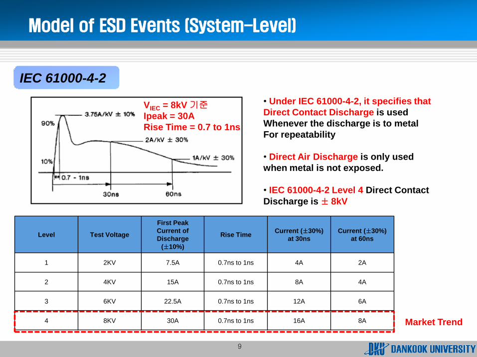
Model of ESD Events (System-Level)
IEC 61000-4-2
VIEC = 8kV 기준Ipeak = 30A
Rise Time = 0.7 to 1ns
• Under IEC 61000-4-2, it specifies that
Direct Contact Discharge is used
Whenever the discharge is to metal
For repeatability
• Direct Air Discharge is only used
when metal is not exposed.
• IEC 61000-4-2 Level 4 Direct Contact
Discharge is ± 8kV
Level Test Voltage
First Peak
Current of
Discharge
(±10%)
Rise TimeCurrent (±30%)
at 30ns
Current (±30%)
at 60ns
1 2KV 7.5A 0.7ns to 1ns 4A 2A
2 4KV 15A 0.7ns to 1ns 8A 4A
3 6KV 22.5A 0.7ns to 1ns 12A 6A
4 8KV 30A 0.7ns to 1ns 16A 8A Market Trend

2. Basic Concept of ESD Protection Circuit

11
• The ESD clamp must not trigger
- under normal circuit operation condition
• The ESD clamp must trigger
- below the oxide breakdown voltage Vox
• Another Condition
- The Lower Ron (on-state R), The Better @within ESD Windows
• The condition of ESD design window
Vdd + 10% < Vclamp =< Vt1 < Vt2 < Vox
• The design window gets narrower with down-scaling Tech.
- The margin between junction and oxide breakdown voltage is
decreasing dramatically and eventually crossed the junction
breakdown voltage.
- New trigger mechanism will have to be found which no longer
rely in the junction breakdown.
- Dynamic trigger schemes suggest reduced trigger voltage voltage.
Cu
rren
t
Voltage
Supply
voltage
range
ma
rgin
Oxide
Break-
down
ESD design
window
Vsp Vt1
Vt2
It2
Ron
ESD Device Design Window

12
Basic Design of ESD Clamp
VSS
I/O
Pin
s
:ESD Clamp :Parasitic Diode :ESD (Surge)
Internal
Circuit
IC Chip
• To protect the IC from such high voltage pulses, ESD clamps are placed
between every I/O pin and power supply pin.
• ESD clamps turn on only when an ESD pulse is detected
And turn off during normal operations.
VDD
VSS
I/O Clamp
Power Clamp
13
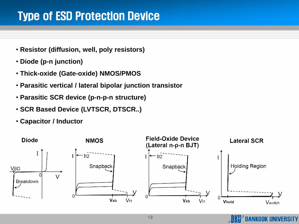
• Resistor (diffusion, well, poly resistors)
• Diode (p-n junction)
• Thick-oxide (Gate-oxide) NMOS/PMOS
• Parasitic vertical / lateral bipolar junction transistor
• Parasitic SCR device (p-n-p-n structure)
• SCR Based Device (LVTSCR, DTSCR..)
• Capacitor / Inductor
Type of ESD Protection Device

Cathode
P-sub
P-Well
N+ P+N+
N-WellN-Well
Anode
GGNMOSFET triggering mechanism in self-biasing mode:
1. Avalanche multiplication by high VD across drain/substrate junction
2. Hole current gives Isub and Ib Voltage drop (Isub*Rsub) across Rsub
3. Source/substrate junction forward biased: Isub*Rsub~0.7V (NPN turns)
4. Effective emitter area is defined by junction sidewall
5. J.E heating at the drain junction causes ESD failure
Second breakdown Oxide breakdown or Metal melting
Drain Voltage (VD)
Dra
in C
urr
en
t (I
D)
Drain-Well
Breakdown
Bipolar Turn-On
VT1, IT1
Bipolar Holding
Voltage
Self-Biased Bipolar
Operation region
Second Breakdown
Trigger Voltage and
Current
Thermal Failure
VH
VT2 ,IT2
GGNMOSFET (Gate Grounded NMOSFET)
* GGNMOSFET in ESD Protection Operation
14

SCR (Silicon Controlled Rectifier)
Anode Cathode
P-Epi
N-Well P-Well
N+ N+P+ P+
SCR triggering mechanism :
1. Avalanche multiplication by high VD across N-Well/P-Well junction
2. VEB of PNP is forward-biased PNP turns on
3. Current through PNP flows into the p-well
4. VEB of NPN is forward-biased NPN turns on
5. NPN current from n-well to cathode Forward-bias for PNP
6. Anode no longer needs to provide the bias for the PNP
Anode Voltage (VA)
An
od
e C
urr
en
t (I
A)
VTrig, ITrigVH
VH : Holding Voltage
• current that the PNP need to
supply to forward-bias the NPN
VTRIG breakdown voltage
of the n-well to sub
On-resistance : ~1Ω
• low power dissipating device
* SCR in ESD Protection Operation
15

16
ESD Protection Circuit
PAD Based ESD Protection
• ESD current is directly shunted from the I/O pin to GND.
• ESD device exists on every I/O pad between the pad and the ground.
• ESD protection devices are usually snapback devices.
16

17
ESD Protection Circuit
Rail Based ESD Protection
• ESD current is redirected to the VDD power rail and then shunted to GND by a power clamp.
• Bus resistance from I/O pins to the power clamps should be accurately estimated.

3. ESD Technology Issue

19
Process Technology (Design Window)
• ESD Design Window
ESD design window shrinks with new CMOS tech.
• VDD Core Supply Voltage
rapid reduction
• Gate Oxide Downscaling
Transient oxide breakdown voltage is decreasing faster with technology advancement.
ESD Device Trigger Issue
Low Voltage ESD Protection Issue
20
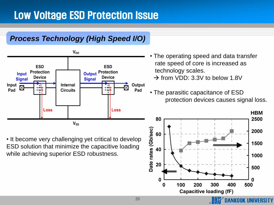
Low Voltage ESD Protection Issue
Process Technology (High Speed I/O)
• The operating speed and data transfer
rate speed of core is increased as
technology scales.
from VDD: 3.3V to below 1.8V
• The parasitic capacitance of ESD
protection devices causes signal loss.
• It become very challenging yet critical to develop
ESD solution that minimize the capacitive loading
while achieving superior ESD robustness.
HBM

Holding Voltage Engineering
High Voltage ESD Protection Issue
Operation
Range
VDD
VH
VH Engineering
VT
• In HV ICs, the Power Supply (VDD) can be over 10V, a few 10V or even higher.
Requirements for automotive IC, e.g. 5V, 20V, 45V, 60V
• Low doping implants to obtain the high breakdown voltage
Low doping concentrations strongly impact the snapback behavior.
• Due to the high operating voltage in applications of HV devices,
all clamps have a high enough holding voltage above VDD.
After transient trigger
40V
< Transient Latch-up Test >21

High Voltage ESD Protection Issue
Area Efficiency
• In HV ICs, HV-ESD protection Device typically leading to very large area consumption
Large Leakage Current, Large Capacitance
• HV-ESD solutions for the Power IC focus on smallest area HV-ESD protection design
Small pad pitch, Small ESD device size
• Circuit Under Pad (CUP) is useful to reduce the ESD protection circuit area
Clamp LayoutIt2
(mA/um2)
HBM
(V/um2)
LV-MOS
StackNon-Silicide 0.24 > 0.56
LV-MOS
StackSilicide 0.63 > 0.56
RC-
MOSFETMin Cap. 0.11 0.66
< Comparison of the current capability per unit area>
DiodeRC-
MOS
PMOS/
PNP
NMOS/
NPNSCR
Area
< Comparison of general High Voltage ESD Device>
PAD
PAD
LV-ESD
LV-ESDLV-ESD
LV-ESD
< LV I/O Clamp & HV Power Clamp in Power IC>
HV-ESD
22

4. ESD Protection Designfor Power IC

*Fast-Substrate Triggering BiCMOS
• Proposed BiCMOS Device
• Area for local protection : 2000um²
• Very Low Trigger Voltage, Fast Turn-on Speed
• 0.13um CMOS process
LV ESD Device Solution for Power IC (MOS Tech)
<Layout View><Schematics>
<TLP I-V Curve>
<Turn-On>
Trigger Voltage : 5.98V
Holding Voltage : 5.71V
It2 : 2.3A
HBM Level : 3kV
MM Level : 210V
24

Trigger Voltage [V] Holding Voltage [V]2nd Trigger Voltage
[V]
Effective Robustness
[A] @ 10V
GGNMOS 9.92 6.58 14.52 1.4
STNMOS 5.85 5.91 10.58 1.68
GSTNMOS 5.31 5.3 11.71 2.23
GSTNMOS TLP I-V Leakage Current
*Gate-Substrate Trigger NMOS (GSTNMOS)
LV ESD Device Solution for Power IC (MOS Tech)
25

26
*PTSCR (P-Substrate Triggered SCR)
• Proposed SCR based Device
• MOS Trigger technique and SCR operation
• Low triggering voltage, High holding voltage, High Holding Current Latch-up immunity
LV ESD Device Solution for Power IC (SCR Tech)
<Layout View> <TLP I-V Curve>
Trigger Voltage : 8~10V
Holding Voltage : 5~7V
It2 : 6~7A
HBM Level : 8kV
MM Level : 940V

*HHVSCR (High Holding Voltage SCR)
LV ESD Device Solution for Power IC (SCR Tech)
• High holding voltage, Latch-up immunity
• Effective ESD performance by SCR based Device
• Extended p+ cathode diffusion and the additional n-well region
• Power Clamp for 10V
• Small area for local protection : 2565um²
<Layout View>
<TLP I-V Curve>
Trigger Voltage : 18.3V
Holding Voltage : 9.8V
It2 : 6.6A
HBM Level : 8kV
MM Level : 720V
27

28
HV ESD Device Solution for Power IC (MOS Tech)
28
< Cross-sectional view >
• ESD protection structure with novel trigger
technique for LDMOS
• The same structure as drain region in LDMOS,
the vertical NPN transistor and the lateral
transistor
• The avalanche current acts as the base current
of NPN transistor.
• The IT2 value is nearly four times as large as
that of the simple LDMOS < TLP I-V characteristics>
< TLP I-V characteristics with small and large R1 resistance>
• Power Clamp for 20V
• 0.6um BCD Process
Modified LDMOSFET
29
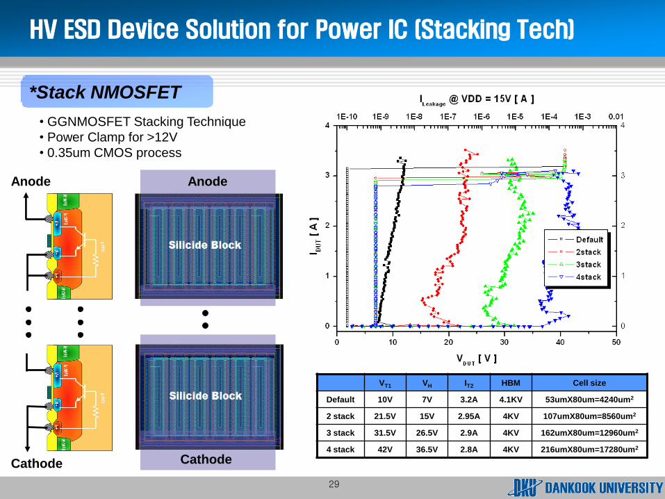
HV ESD Device Solution for Power IC (Stacking Tech)
*Stack NMOSFET
• GGNMOSFET Stacking Technique
• Power Clamp for >12V
• 0.35um CMOS process
Anode
Cathode
VT1 VH IT2 HBM Cell size
Default 10V 7V 3.2A 4.1KV 53umX80um=4240um2
2 stack 21.5V 15V 2.95A 4KV 107umX80um=8560um2
3 stack 31.5V 26.5V 2.9A 4KV 162umX80um=12960um2
4 stack 42V 36.5V 2.8A 4KV 216umX80um=17280um2
Anode
Cathode

30
Segmented SCR
N-Ext P-Ext
N+ P+ N+ P+
N-Ext P-Ext
N+
P+
N+
P+
P+
P+
P+
P+
P+
N+
N+
N+
N+
N+
• SCR structure with high holding voltage ( ~ 40V )
Reduced the emitter injection efficiency of the parasitic BJTs in the SCR.
• Latch-up immunity and high failure current for ESD robustness
< Conventional > < Segmented SCR >
HV ESD Device Solution for Power IC (SCR Tech)
31
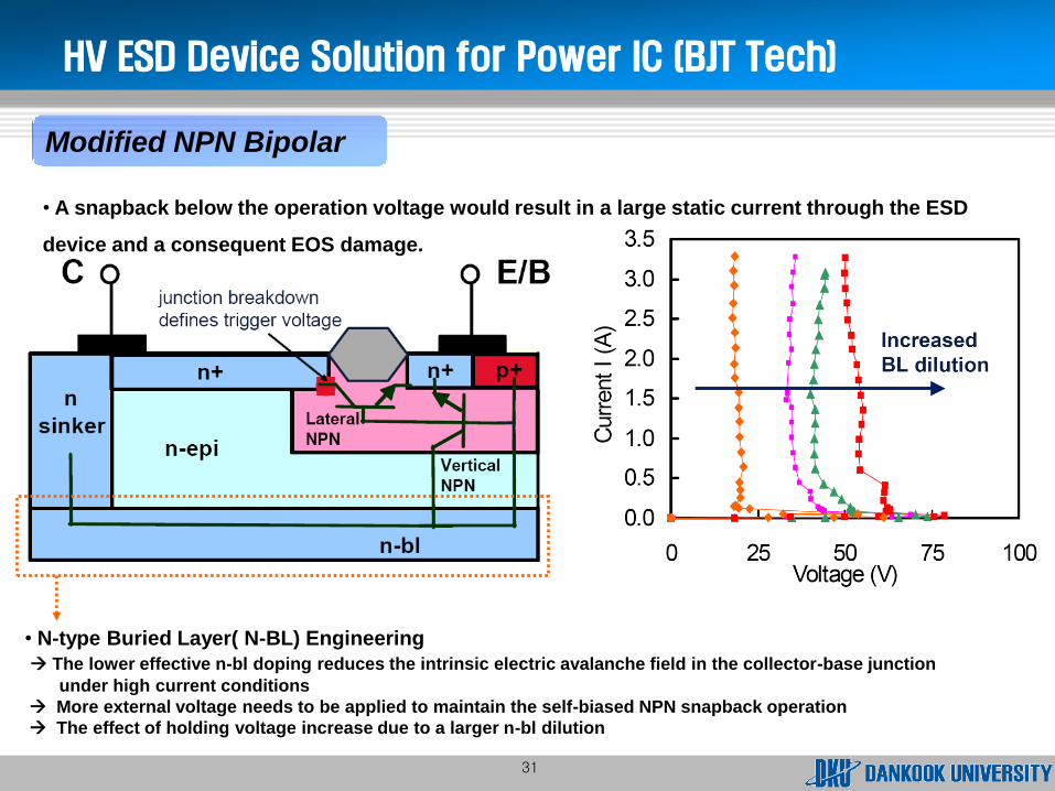
Modified NPN Bipolar
• N-type Buried Layer( N-BL) Engineering
The lower effective n-bl doping reduces the intrinsic electric avalanche field in the collector-base junction
under high current conditions
More external voltage needs to be applied to maintain the self-biased NPN snapback operation
The effect of holding voltage increase due to a larger n-bl dilution
• A snapback below the operation voltage would result in a large static current through the ESD
device and a consequent EOS damage.
HV ESD Device Solution for Power IC (BJT Tech)
32
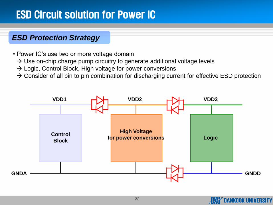
• Power IC’s use two or more voltage domain
Use on-chip charge pump circuitry to generate additional voltage levels
Logic, Control Block, High voltage for power conversions
Consider of all pin to pin combination for discharging current for effective ESD protection
Control
Block
High Voltage
for power conversions Logic
VDD1
GNDA
VDD2 VDD3
GNDD
ESD Protection Strategy
ESD Circuit solution for Power IC

33
ESD Protection Scheme for Mixed Supply Voltage
ESD Clamp Coupling Diode
In InCircuit I Circuit II
VSS-LV
Po
wer
Cla
mp
Po
wer
Cla
mp
Out Out
VDD-LV
VSS-HV
VDD-HVESD Cell
:HV ESD Clamp :Parasitic Diode:LV ESD Clamp:Coupling Diode
ESD Circuit solution for Power IC

34
ESD Protection Scheme with ESD Buses
Circuit I Circuit II Circuit III
ESD
Conduction
Circuit
ESD
Conduction
Circuit
ESD
Conduction
Circuit
ESD
Conduction
Circuit
ESD
Conduction
Circuit
ESD
Conduction
Circuit
Po
we
r-R
ail
ES
D C
lam
p C
ircu
it
Po
we
r-R
ail
ES
D C
lam
p C
irc
uit
Po
we
r-R
ail
ES
D C
lam
p C
irc
uit
Po
we
r-R
ail
ES
D C
lam
p C
irc
uit
VDD1
VSS1
VDD2
VSS2
VDD3
VSS3
VDD ESD Bus
VSS ESD Bus
ESD Circuit solution for Power IC

35
*ESD Protection Circuit for Touch Screen Driver IC
• I/O Frequency 1.1Ghz ( < 0.5pF )
• ESD Protection Device: PTSCR
• HBM >7kV, MM >600V , IEC61000-4-2 4kV
• Area (BPAD: 70umX70um, Device: 50umX 70um
Whole Chip ESD Protection Circuit Design
<HBM 7kV PASS> <HBM 8kV FAIL>
< Layout Top-view >
< ESD Device DC-IV curve after HBM zap tester>
PTSCR
DIODE
BPAD

36
*ESD Protection circuit for LED Driver IC
Whole Chip ESD Protection Circuit Design
• HBM 8kV, MM 800V Pass
• Area (< 2600um2)
• Output current per channel : 100mA
• The use of SCR based ESD device
IO & Power
ESD DeviceDesign Factor
HHVSCR Width = 57um, Length = 45um
• The ESD device solution for Power ICs :
37
Summary
• Power IC’s ESD Strategy : Area efficiency, Latch-up immunity, ESD
robustness, Consider of all pin to pin combination
• ESD Technology Issue : Design window, High Speed I/O
High Holding Engineering, Area Efficiency, Process Technology
• ESD protection is a very high priority for Power ICs reliability
- Low Voltage : MOS, SCR based ESD Protection Device etc.
- High Voltage : R-C LDMOS, BJT, SCR, Stack based ESD Protection Device etc.