Embed Size (px)
Citation preview

1 | P a g e
POWER FACTOR IMPROVEMENT OF SINGLE PHASE AC-DC SYSTEM
USING PARALLEL BOOST CONVERTER
A thesis submitted in partial fulfillment in the requirements for the degree of
BACHELOR OF TECHNOLOGY
IN
ELECTRICAL ENGINEERING
BY
PEMA RABDEN
ROLL NO.-111EE0564
Under the guidance of
Prof .A.K.PANDA
DEPARTMENT OF ELECTRICAL ENGINEERING,
NATIONAL INSTITUTE OF TECHNOLOGY,
ROURKELA

2 | P a g e
National Institute Of Technology
Rourkela
CERTIFICATE
This is to certify that the project entitled, “POWER FACTOR IMPROVEMENT OF SINGLE PHASE
AC-DC SYSTEM USING PARALLEL BOOST CONVERTER”
Submitted by Pema Rabden (Roll no-111EE0564) is an authentic piece of project carried out by him under
my supervision and guidance for the partial fulfillment of the requirements for the award of Bachelor of
Technology Degree in Electrical Engineering at National Institute of Technology, Rourkela
To the best of my knowledge, the matter and content embodied in the project has not been submitted to any
other University / Institute for the award of any degree / diploma.
Prof.A.K.Panda
Prof and HOD
Department of Electrical Engineering, NIT, Rourkela

3 | P a g e
ACKNOWLEDGEMENT
Upon the submission of my thesis report of my project on “Power Factor improvement of single phase
AC-DC system using parallel boost converter”, I would like to extend my deep gratitude and my sincere
thanks to my esteemed, honorable guide Prof. A K PANDA, HOD, Department of Electrical Engineering
for giving me the opportunity to work in the field of power factor improvement. This project has given me
enough scope of research oriented study. I really acknowledge and esteem his regarded direction and
consolation from the earliest starting point to the end of this thesis. I am indebted to him for helping me
correct the problem and supporting me throughout my project.
I would like to thank research scholars in Power Electronics Lab and my batch mates for helping me with
the valuable tips in obtaining the correct simulation results. And thanks to all those mates who helped me
complete my projecct in time.
I am thankful for the constant moral support of my parents and friends without which it would have been
tough for me to complete this work.
Pema Rabden
B.Tech, Electrical Engineering
NIT ROURKELA, ODISSHA

4 | P a g e
Abstract
Power factor in an AC electrical power system is described as the ratio of the actual power passing
though the load to the virtual power flowing through the circuit or the cosine angle of the potential
and charge of an AC circuit. A phase difference Ø exists between the potential and charge of an
AC circuit and cosine which is called the circuit’s power factor. Suppose we get an inductive
circuit we generally get the lagging by the voltage and that will be called a lagging power factor.
And suppose we get the capacitive circuit then the current will be leading by the voltage and that
will be referred as a leading power factor.
The usage of power electronic system has reached to a new application stage that include
residential, commercial, and aerospace and many others. Power electronic interfaces e.g. Switch
Mode Power Supplies (SMPS) have proved to be superior over traditional linear power supplies.
However their nonlinear behavior puts a question mark on their efficiency. The current drawn by
the SMPS from the line is distorted resulting in a high Total Harmonic Distortion (THD) and low
Power Factor (PF). Other adverse effects on the power system includes increased magnitudes of
neutral current in three phase systems, overheating of transformers and induction motors etc.
Therefore there is a continuous need of power factor improvement and reduction of line current
harmonics. A large range of PFC circuits have been proposed with diverse operating modes to
solve the situation. These PFC circuits adjust the waveforms of the current in the input side so that
the maximum power can be tapped from the supplies. For every equipment the load should try to
match a resistive one as closely as possible, only then the PF will be near to unity as there will be
reduction of reactive power in the circuit. The current in this situation is free from all the lower as
well as higher order harmonics thus copies the input voltage waveform. So this causes the current
in the circuit to be at the lowest possible value to do the same work. As a result, the losses
associated with circuit are reduced. Hence the consumption in power is reduced greatly. Boost
converter accomplishes this active power-factor correction (ACMC) in discontinuous as well as in
continuous modes.
Simulation of a single phase bridge converter without using any converter is performed first. Then
a current control circuit and a voltage control circuit were added to the boost converter which
improved the input THD.
This project aims to develop a circuit for power factor improvement using two Boost converters
connected in parallel. It is based on the power sharing method to improve the current quality and
to reduce the switching losses. In this method current in one circuit has to keep up with the one in
parallel to it.

5 | P a g e
CONTENTS
Abstract 4
Contents 5
List of figures 6
List of tables 7
1. Introduction
1.1 Description of Power Factor 9
1.2 Harmonics 12
1.3 The problem of Power Factor in single phase line commutated rectifiers 12
1.4 Power Factor and Total Harmonic Distortion 13
1.5 Standards for line current harmonics 15
2. Power Factor Correction
2.1 Passive Power Factor Correction 18
2.2 Active Power Factor Correction 21
3. DC-DC Converters
3.1 Basic circuit topologies of active power factor corrector 24
3.2 Working principle of Boost converter 25
3.3 Transfer Function of a Boost converter 27
4. Control methods of DC-DC converters
4.1 Peak Current Mode Control 30
4.2 Average Current Mode Control 31
5. Parallel connection of two Boost converters
5.1 Circuit modeling for dual Boost PFC 35
5.2 Control of Dual PFC 36
Results and simulation 38
Conclusion 44
References 45

6 | P a g e
LIST OF FIGURES
1. FIG 1 Block diagram regarding AC-DC system 11
2. FIG 2 Single Phase Rectifier 12
a) Circuit
b) Waveforms of input voltage and current
3. FIG 3 Graph between PF and THD (%) 15
4. FIG 4 A passive PFC circuit 18
5. FIG 5 Rectifier circuit using inductive input filter 19
6. FIG 6 Rectifier circuit using resonant input filter 20
7. FIG 7 Block diagram of active PFC technique 21
8. FIG 8 Different types of single phase PFC topologies 22
9. FIG 9 On and off states of a Boost rectifier 25
10. FIG 10 Behavior of inductor current. 26
(a) Waveforms
(b) Transistor T gate drive signal x
11. FIG 11 Peak Current Mode Control and its wave form 30
12. FIG 12 Average current control method 32
13. FIG 13 34
(a): PFC circuit
(b): Dual Boost PFC circuit
14. FIG 14 37
(a) Input currents of two interleaved PFC circuits
(b) Input currents of two interleaved PFC circuits in ideal working condition
(c) Input currents of two PFC circuits based on internal active filtering
15. FIG 15 Simulation block of rectifier 38
Circuit without any PFC

7 | P a g e
16. FIG 16 Plot of input voltage and input current vs time 39
for rectifier circuit without any PFC
17. FIG 17 Simulink block of rectifier circuit with 39
Boost converter for PFC using average current mode control
18. FIG 18 Plot of input current vs time for a rectifier circuit 40
with Boost converter as PFC circuit using average current mode control method.
19. FIG 19 Plot of input voltage and input current vs time for rectifier 40
circuit with Boost converter as PFC circuit using average current
mode control method
20. FIG 20 Output voltage for a rectifier circuit with Boost 40
converter as PFC using average current mode control method.
21. FIG 21 Simulation block for rectifier circuit with parallel Boost converter. 41
22. FIG 22 Plot of input current vs time for a rectifier 41
circuit with parallel Boost converter
23. FIG 23 Plot of input voltage and input current vs time for 42
rectifier circuit with parallel Boost converter.
24. FIG 24 Output voltage for a rectifier circuit with parallel Boost converter 42
LIST OF TABLES
1. Table 1 Power Factor vs Total Harmonics Distortion (in %) 14

8 | P a g e
INTRODUCTION
POWER FACTOR
HARMONICS
THE PROBLEM OF POWER FACOR IN A SINGLE
PHASE LINE COMMUTATED RECTIFIER
POWER FACTOR AND TOTAL HARMONIC
DISTORTION
STANDARDS FOR LINE CURRENT HARMONICS

9 | P a g e
CHAPTER1: INTRODUCTION
1.1 POWER FACTOR:
Power factor in an AC electrical power system is described as the ratio of the actual power passing
though the load to the virtual power flowing through the circuit or the cosine angle of the potential
and charge of an AC circuit. A phase difference Ø exists between the potential and charge of an
AC circuit and cosine which is called the circuit’s power factor. Suppose we get an inductive
circuit we generally get the lagging by the voltage and that will be called a lagging power factor.
And suppose we get the capacitive circuit then the current will be leading by the voltage and that
will be referred as a leading power factor.
In an electrical power system, a low power factor load draws greater current than a higher power
factor load for the equivalent ratio necessary power passed.
Power factor provides a ratio which shows the effectiveness of the actual power utilized in the
system. It is a measure of distortion of the line current and their phase change.
Power factor= Real power (average)/Apparent power
The virtual power is known as the multiplication of the rms value of current and voltage. We can
describe the real power like the power of the circuit for doing work in some known interval of
time.
LINEAR SYSTEMS:
For linear system, the load generally puts out clear sine voltage and current, so we can know about
the Power factor jut by the change in phase of voltage and current.
I.e. PF=cos Ø
In a totally resistive circuital current and voltage graphs are in step (or in phase), if we reverse the
polarity at the same interval for every cycle. The power getting into the load is utilized. A linear
load never changes the structure of the graphs of the current, but it may differ the combined timing
of the generated current and voltage.

10 | P a g e
Purely resistive load waveform..
Some loads which are inductive like transformers and also motors intake power which is reactive
and we get the lagging current waveform than the voltage. Capacitor banks which gives loads
which are Capacitive produce extra power which is reactive and we get the leading current phase
than the voltage.
Purely inductive load waveform
The different applications for AC-DC converters are speed drives which are adjustable. Switched Mode
Power systems (SMPS), UPS, etc. Diode rectifiers can be utilized for the applications of different Power
Electronic devices which are in connection with the AC utility mains. We can get the non-linear nature of
the Diode rectifier and due to this we get harmonics in the current line, so due to this the destruction of the
power quality which in turn increase the various losses in the device. In the beginning the capacitors and
the inductors were very costly and they were used or decreasing the harmonics. Active Power Line
Conditioners (ALPC) that were utilized for decreasing the harmonics are switched hard, which causes low
efficiency. There are the Boost converter topology in which there is a continuous conduction mode (CCM)
is put in medium power AC/DC converter, as they provide a power factor which is nearly equal to unity if
we see from the input side of the terminals which is in this case is AC.

11 | P a g e
FIG-1. Block diagram regarding AC-DC system.
The power which is given in the AC line is the multiplicative product of the rms values of the voltage
current signals.
We call this power “apparent power”.
𝑃𝐴 = 𝑉𝑟𝑚𝑠𝐼𝑟𝑚𝑠
Actual Power is provided by the product of the instantaneous current and voltage and then we
are supposed to get the result by averaging the product.
𝑃𝑅 =
1𝑇 ∫ 𝑣(𝑡) 𝑖(𝑡)𝑑𝑡
Where,
𝑣(𝑡)= instantaneous voltage signal
𝑖(𝑡)= instantaneous current signal
1.2 HARMONICS:
As the non-linear interrelation of the voltage and current throughout the switching devices,
harmonic is produced by each type of switching converters. We can also produce Harmonics by
the equipment’s which are conventional which includes:
1. Equipment that generates power (slot harmonics).

12 | P a g e
2. Induction motors (saturated magnetics).
3. Transformers (saturation happens due to over excitation).
4. Magnetic-ballast fluorescent lamps (arcing) and
5. AC electric arc furnaces.
These are the above mentioned devices that are responsible for the flow of the harmonic current
and there are some devices which directly creates voltage harmonics.
1.3 THE PROBLEM OF POWER FACTOR IN SINGLE PHASE LINE
COMMUTATED RECTIFIERS:
These are the following disadvantages of the Classical line commuted rectifiers:
1. A lagging displacement factor is produced with respect to the utility’s voltage.
2. A considerable amount of input current harmonics is generated.
These are the aspects which somewhat affects the power factor as well as the quality of power.
Fig.2: Single Phase Rectifier a) Circuit b) waveforms of input voltage and current

13 | P a g e
1.4 POWER FACTOR AND TOTAL HARMONIC DISTORTION:
The ratio of summation of rms values of current harmonics with the squared root mean value of
the primary component of the current is called the Total harmonic distortion of the current.
𝑇𝐻𝐷 =[∑ 𝐼𝑛𝑟𝑚𝑠
2 ]∞𝑛=2
0.5
𝐼1
So,
𝐼1
𝐼𝑟𝑚𝑠=
1
√1 + 𝑇𝐻𝐷2= 𝑘𝑝
Where 𝑘𝑝 is the distortion factor
So, the power factor’s expression becomes
𝑃𝐹 = 𝑘𝑝𝑐𝑜𝑠𝜃
The table tells us the power factor and the percentage of the THD.This data which is shown in the
table tells us whether the power factor is smaller compared to 0.7, the combined harmonics rms
value is more than primary rms value.SO we can clearly see that the efficiency which is smaller
than 50% as we know that the power which is delivered only at primary frequency.
14 | P a g e
TABLE 1
Power Factor versus percentage of THD
(𝜽 = 𝟎, cos𝜽=1)
Power Factor THD (in percentage)
0.5 174.21%
0.7 102.12%
0.9 48.53%
0.96 29.36%
0.98 20.41%
0.992 12.53%
0.995 10.34%
0.997 7.78%
0.999 4.58%
0.9992 4.40%
0.9996 2.73%
1 0.00%
15 | P a g e
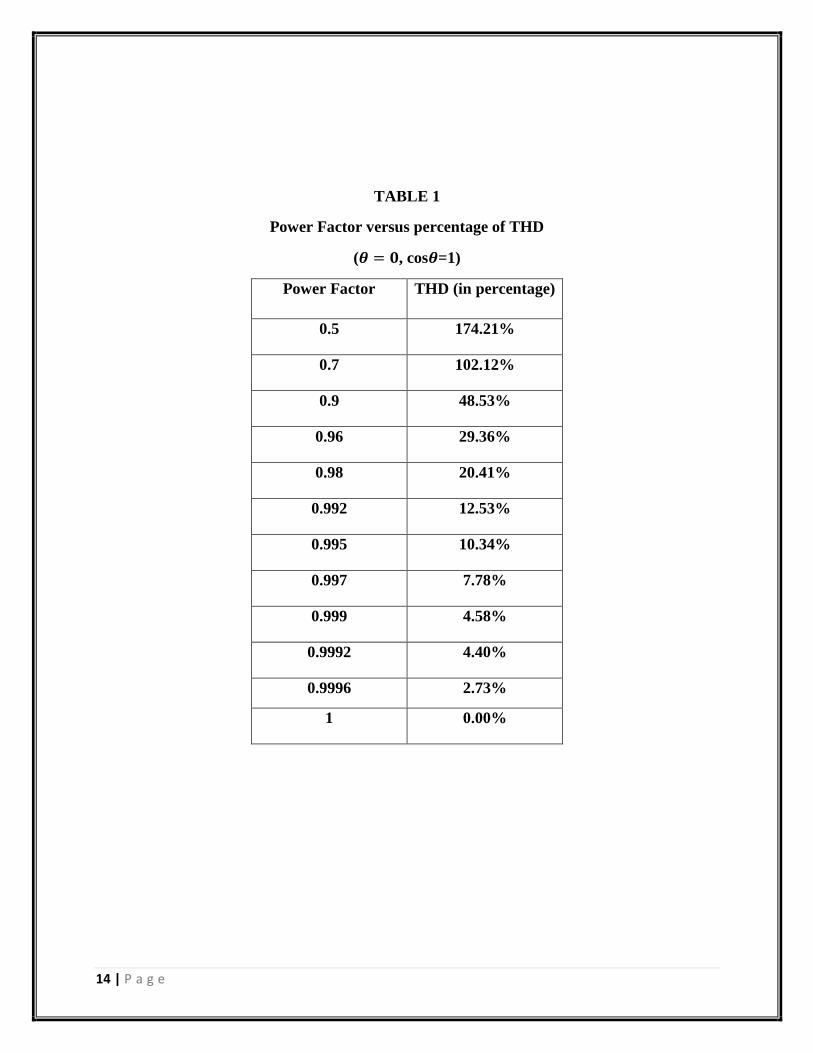
Power Factor versus Percentage of THD
(𝜽 = 𝟎, cos𝜽=1)
Fig 3: Graph between PF and THD(%)
1.5 STANDARDS FOR LINE CURRENT HARMONICS:
STANDARD IEC 1000-3-2:
1. The standard which we consider are those instruments whose current rating is up to. It uses
16A per phase and at the same instant it is supposed to be in connection to 50Hz/60Hz,
220-240Vrms if we are considering one phase system or 380-415Vrms if we are
considering three phase system.
2. The types of the electrical equipment according to this standard are four which are A, B,
C, and D.

16 | P a g e
3. Not taking the lighting equipment’s consider only those equipment’s which have rated
power less than 75W.
CLASS-A:
Instruments only comes under class A which are not given in the remaining classes.
CLASS-B:
Class B contains the instruments which are portable that is the welders that are amateur in
character.
CLASS-C:
Except the dimmers the remaining equipment’s that are required for lighting purposes
comes under class C.
CLASS-D:
The equipment’s that are having an active input power less than or equal compared to
600W.
The important equipment that comes under this are PC, Monitors, TV sets.
STANDARD IEEE 519-1992:
It boosts the use of control harmonics in various power system for particular consumer and
also in the form of utilities. The involved harmonics of the line current are known as the
percentage of greatest usable load current 𝐼𝐿 demand. If we reduce 𝐼𝑠𝑐
𝐼𝐿 it automatically
reduces, which shows that the less firm grids have generally less limits.

17 | P a g e
POWER FACTOR CORRECTION
PASSIVE POWER FACTOR CORRECTION
ACTIVE POWER FACTOR CORRECTION

18 | P a g e
CHAPTER2: POWER FACTOR CORRECTION
2.1 PASSIVE POWER FACTOR CORRECTION
Harmonics current is controlled in an easiest possible way with the help of a designed filter which
passes through only at line frequency (50 or 60Hz). Harmonic currents are pressed down to make
the non-linear instruments seems linear. Power factor that can be corrected with the use of
capacitors and inductors which are passive devices. These filters are basically called passive filters
because they are passive devices.
A passive PFC circuit needs just some basic devices to level up the output ratio that is efficiency,
but they are big because of their working at the line power frequency.
Fig 4: A passive PFC circuit.
The basic ways for improving passive power factor is by using:
1. Inductive input filter.
2. Resonant input filter.
2.1.1INDUCTIVE INPUT FILTER
Inductive input filters are not totally same from capacitive input filters because of the added
inductor in it. Capacitor voltage in capacitive filter is charged and also to a maximum input voltage.
19 | P a g e
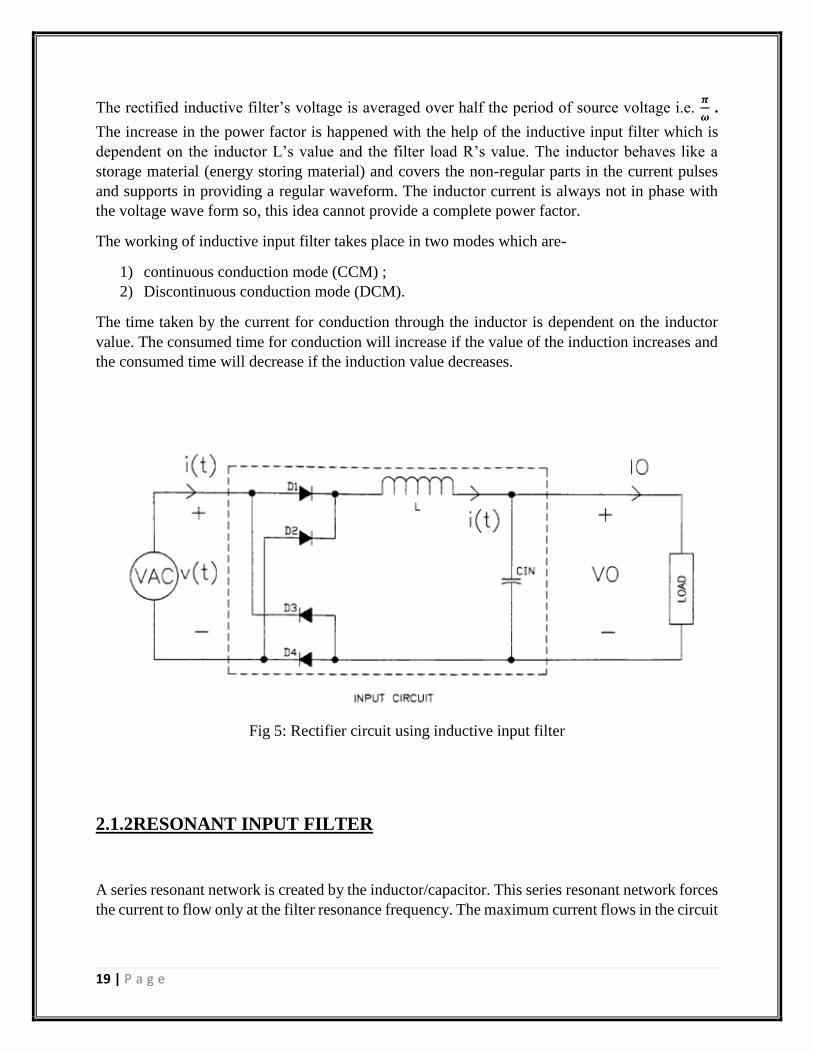
The rectified inductive filter’s voltage is averaged over half the period of source voltage i.e. 𝝅
𝝎 .
The increase in the power factor is happened with the help of the inductive input filter which is
dependent on the inductor L’s value and the filter load R’s value. The inductor behaves like a
storage material (energy storing material) and covers the non-regular parts in the current pulses
and supports in providing a regular waveform. The inductor current is always not in phase with
the voltage wave form so, this idea cannot provide a complete power factor.
The working of inductive input filter takes place in two modes which are-
1) continuous conduction mode (CCM) ;
2) Discontinuous conduction mode (DCM).
The time taken by the current for conduction through the inductor is dependent on the inductor
value. The consumed time for conduction will increase if the value of the induction increases and
the consumed time will decrease if the induction value decreases.
Fig 5: Rectifier circuit using inductive input filter
2.1.2RESONANT INPUT FILTER
A series resonant network is created by the inductor/capacitor. This series resonant network forces
the current to flow only at the filter resonance frequency. The maximum current flows in the circuit

20 | P a g e
only when the inductive reactance is equal to the capacitive reactance and this is achieved only at
the resonant frequency.
The resonant frequency and the characteristics impedance define the resonant input filter, given
by the expression
𝜔𝑅=
1
√𝐿𝐶
and
𝑍𝑅= √
𝐿𝐶
To get the maximum power factor the input line frequency and the resonant frequency are both
made same.
𝜔𝑅 = 𝜔
The output DC voltage of the storage capacitor gives the DC current in load designed as R.
Fig 6: Rectifier circuit using resonant input filter

21 | P a g e
2.2 ACTIVE POWER FACTOR CORRECTION
An active power factor improvement is the finest method to improve rise the power factor in power
drives. In this method we use a boost converter and we place it in the middle of the bridge rectifier
and the main input capacitors. The converter establishes a constant DC output bus voltage and
attains a current which is in similarity with and at the equivalent line voltage frequency.
The active PFCs trims the waveform for eliminating all the unnecessary harmonics by
transforming the current put out from the line power at the converter‘s operating frequency. Out
of all the topologies the most efficient as PFC converter is Boost converter. By analyzing all the
topologies Buck converter is most disadvantageous because it needs extra input filter to eliminate
the operating pulsating input current’s frequency material. The Buck-Boost and fly back converters
are generally utilized in less energy devices and is generally not suitable for greater power usages
in which the improvement of factor correction is essential.
Fig 7: Block diagram of active PFC technique

22 | P a g e
Fig 8: Different types of single phase PFC topologies
ACTIVE PFC FUNCTIONS:
1. Modelling of Active wave of the input current.
2. Trimming high operating frequency.
3. The source current’s Feedback sensing for waveform control.
4. Regulation of output voltage by Feedback control.

23 | P a g e
DC-DC CONVERTER
BASIC CIRCUIT TOPOLOGIES OF ACTIE
POWER FACTOR CORRECTOR
WORKING PRINCIPLE OF BOOST
CONVERTER
TRANSFER FUNCTION OF BOOST
CONVERTER
24 | P a g e
CHAPTER 3: DC-DC CONVERTERS
Power electronic converters are normally used to convert electricity from one form to other forms.
They form an interface between source and load side.
High-frequency active PFC circuits are used for power factor correction. If a proper control method
is used to shape the input currents, any DC-DC converter can be used for power factor correction.
The DC-DC converters can operate in Continuous Inductor Current Mode (CICM), where the
inductor current never reaches zero in one switching cycle or Discontinuous Inductor Current
Mode (DICM), where the inductor current is zero during the intervals of the switching cycle.
Various types of control techniques are used to control the inductor current in Continuous Inductor
Current Mode. Some of the techniques used are (1) Peak Current Control (2) Average Current
Control (3) Hysteresis Control (4) Borderline Control. The average mode control technique is
specifically developed for PFC boost converters and is analyzed here.
3.1 BASIC CIRCUIT TOPOLOGIES OF ACTIVE POWER FACTOR
CORRECTOR
The basic circuit topologies of active PFC converter:
1. Buck corrector
2. Boost corrector
3. Buck-Boost corrector
4. Cuk, Sepic and Zeta correctors
Boost rectifiers which is one of the most important high power factor rectifier is used. It is obtained
from a classical non-controlled bridge rectifier with the addition of transistor, inductor and diode.

25 | P a g e
3.2 WORKING PRINCIPLE OF A BOOST CONVERTER
Fig 9: On and off states of a Boost rectifier.
The input current 𝑖𝑠(t) can be controlled by changing the transistor conduction state. By giving
appropriate firing pulse to the transistor it is switched on. The waveform of the input current can
be controlled to follow a sinusoidal reference.

26 | P a g e
Fig 10 : Behavior of inductor current.
(a): Waveform
(b): Transistor T gate drive signal x
This figure above shows the reference inductor current 𝑖𝐿𝑟𝑒𝑓 , the inductor current 𝑖𝐿, and the gate
drive signal for transistor. At x=1the transistor is ON and it’s OFF at x=0. The ON and OFF state
of the transistor produces and increase and decrease in the inductor current 𝑖𝐿.

27 | P a g e
3.3 TRANSFER FUNCTION OF A BOOST CONVERTER
The line-to-output transfer function is obtained by taking fluctuations in duty cycle to be zero
and hence:
𝐺𝑣𝑔(𝑠) =𝑣(𝑠)
𝑣𝑔(𝑠)| �̂�(𝑠) = 0
Its importance lies in designing of an output voltage regulator.
The control-to-output transfer function is achieved by taking the input voltage fluctuations to
zero, and hence:
𝐺𝑣𝑑(𝑠) =𝑣(𝑠)
�̂�(𝑠)| 𝑣𝑔(𝑠) = 0
This transfer function shows the influence on the output voltage by varying the control input.
Referring to the small-signal equivalent model, the transfer function is calculated as:
𝐺𝑣𝑔(𝑠) =𝑣(𝑠)
�̂�(𝑠)=
1
𝐷′
(𝑅‖1
𝑠𝐶)
(𝑅‖1
𝑠𝐶 +𝑠𝐿𝐷′2)
=𝐷′𝑅
𝐷′2𝑅 + 𝑠2𝑅𝐿𝐶 + 𝑠𝐿
Comparing the standard form as:
𝐺𝑣𝑔(𝑠) = 𝐺𝑔0
1
1 +𝑠
𝑄𝑤0+ (
𝑠𝑤0
)2
We get,
𝐺𝑔0 =1
𝐷′
𝑄 = 𝐷′𝑅√𝐶
𝐿
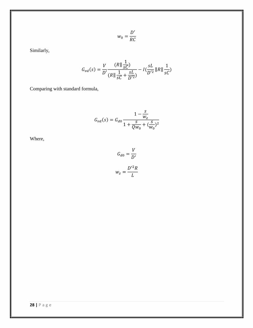
28 | P a g e
𝑤0 =𝐷′
𝑅𝐶
Similarly,
𝐺𝑣𝑑(𝑠) =𝑉
𝐷′
(𝑅‖1
𝑠𝐶)
(𝑅‖1
𝑠𝐶 +𝑠𝐿𝐷′2)
− 𝐼(𝑠𝐿
𝐷′2‖𝑅‖
1
𝑠𝐶)
Comparing with standard formula,
𝐺𝑣𝑑(𝑠) = 𝐺𝑑0
1 −𝑠
𝑤𝑧
1 +𝑠
𝑄𝑤0+ (
𝑠𝑤0
)2
Where,
𝐺𝑑0 =𝑉
𝐷′
𝑤𝑧 =𝐷′2𝑅
𝐿
29 | P a g e
CONTROL METHODS OF DC-DC
CONVERTERS
PEAK CURRENT MODE CONTROL
AVERAGE CURRENT MODE CONTROL

30 | P a g e
CHAPTER4: CONTROL METHODS OF DC-
DC CONVERTERS
4.1PEAK CURRENT MODE CONTROL
FIG 11: Peak Current Mode Control and its wave form
The work of the inner loop is to control the averaged inductor current. The switch current is equal
to the inductor current during ON time. The peak current control is equivalent to the average
inductor current control if the inductor ripple current is small or negligible. In Buck topology, the
inductor current is in the output and in the Boost topology the inductor current is in the input. Thus
the input current is controlled by the current mode control and thus desired waveform can be
obtained.
In this method inductor current is compared with the reference current achieved from the outer
control circuit. And when the value of instantaneous current is equal to the reference current the
power switch is turned OFF by using a comparator.
4.1.1DRAWBACKS OF PEAK CURRENT CONTROL
(a) IMMUNITY TO NOISE IS POOR
Due to smaller instantaneous current compared to the reference current, the circuit is noisy. During
the initial period more noises are observed in the circuit. Therefore voltage signal of low magnitude
causing increment in the ripples associated with the circuit.

31 | P a g e
(b) REQUIREMENT OF SLOPE COMPENSATION
If the duty ratios exceeds 0.5 then the peak current control method is unstable thus results in ripples
and harmonics. Therefore in order to make it stable a slope compensation is required. In a buck
regulator, the slope of current through the inductor is𝑉0
𝐿. But in a Boost regulator the slope of a
current depends on the input voltage. This helps in reduction of distortions in the circuit and helps
the circuit perform well.
(c) PEAK TO AVERAGE CURRENT ERROR
The low magnitude in the current results in the discontinuous waveform of the inductor current.
While the peak current follows the sine wave current program and the average current does not
follow it. In order to obtain low distortion the peak error/ the average error should be small.
Therefore for this purpose a large inductor is required. Due to the use of large inductor, it makes
the already poor immunity to noises worse.
(d) TOPOLOGY PROBLEMS
The peak current mode controls the inductor current in the output side. This method is used only
in buck converters where the inductor configuration is on the output side of the circuit. Therefore
this method is only applicable for buck topologies where as for other schemes it will lead to the
control of the wrong current.
4.2AVERAGE CURRENT MODE CONTROL
The average current mode control has two loops, the inner loop which controls the current and the
outer loop which controls the voltage. This control method is applicable in higher switching
frequency. Since this method is advantageous than the peak current mode control method, it is
mostly used for the control of DC-DC converters and single phase power factor correctors.
Advantage of average current mode control over peak current mode control are as follows:
1. There is no requirement of compensation ramp.
2. At low frequency high DC gain is obtained.
3. Immunity to noises are better.
4. The increased DC gain at low frequencies are used for single phase AC-DC conversion
using boost circuits.

32 | P a g e
FIG 12: Average current control method.
According to figure above the current sensor gain is given by
𝑉𝑎(𝑡) = 𝑖𝑔(𝑡)𝑅𝑆
When the error signal is small
𝑉𝑎(𝑡) = 𝑉𝑟𝑒𝑓(𝑡)
And the expression for 𝑅𝑒 is obtained as
𝑅𝑒 =𝑅𝑠
𝑘𝑥𝑣𝑐𝑜𝑛𝑡𝑟𝑜𝑙(𝑡)

33 | P a g e
PARALLEL CONNECTION OF TWO
BOOST CONVERTERS
CIRCUIT MODELLING FOR DUAL BOOST
PFC
CONTROL OF DUAL PFC

34 | P a g e
CHAPTER 5: PARALLEL CONNECTION OF
TWO BOOST CONVERTERS
Parallel connection of two Boost converters give greater efficiency as their capacity is enhanced.
But it can act in different unknown ways due to the non-linear nature of the system.
Designing this system aims to make the current share between the two converters. Practically two
voltage sources are impossible to be connected in parallel connection. But it may work if a proper
control circuit is designed. Hence the Average current mode control is used to solve this problem.
In this method one converter is phase shifted from its counterpart. The main advantages of this
method are:
1. High reliability.
2. Cheap, portable and compact.
3. Greater reduction of ripples in input current.
4. Reduction in loses due to conduction.
5. The size of the inductor and capacitor is also reduced.
Boost converters are used in active power factor corrector. In recent years dual boost converters
are used where two boost converters are connected in parallel. The circuit diagrams are shown
below:
FIG 13 (a): PFC circuit.

35 | P a g e
FIG 13 (b): Dual Boost PFC circuit.
Parallel scheme is used here where the choke 𝐿𝑏1 and the switch 𝑇𝑏1 are for main power factor
corrector and choke 𝐿𝑏2 and switch 𝑇𝑏2 are for active filtering. The filtering circuit improves the
quality of line current reduces the switching losses. Switching losses are reduced because of
different values of switching frequencies and current amplitude.
5.1 CIRCUIT MODELLING FOR DUAL BOOST PFC
Referring to figure 5(b) equations of voltages are found out:
𝑣𝑔 = 𝐿𝑝1
𝑑𝑖𝑝1
𝑑𝑡 𝑅1 𝑖𝑝1 + 𝑓𝑝1𝑣𝑑
𝑣𝑔 = 𝐿𝑝2
𝑑𝑖𝑝2
𝑑𝑡 𝑅2 𝑖𝑝2 + 𝑓𝑝2𝑣𝑑
𝑖𝑃𝐹𝐶 = 𝑖𝑝1 + 𝑖𝑝2
Where,
𝑣𝑔(𝑡) = | 𝑉𝑔 sin (𝑤𝑡)|
𝑓𝑝1 = {0 𝑤ℎ𝑒𝑛 𝑇𝑝1 = 1 (𝑠𝑤𝑖𝑡𝑐ℎ 𝑜𝑛)
1 𝑤ℎ𝑒𝑛 𝑇𝑝1 = 0 (𝑠𝑤𝑖𝑡𝑐ℎ 𝑜𝑓𝑓)}

36 | P a g e
𝑓𝑝2 = {0 𝑤ℎ𝑒𝑛 𝑇𝑝2 = 1 (𝑠𝑤𝑖𝑡𝑐ℎ 𝑜𝑛)
1 𝑤ℎ𝑒𝑛 𝑇𝑝2 = 0 (𝑠𝑤𝑖𝑡𝑐ℎ 𝑜𝑓𝑓)}
𝑣𝑔(𝑡) , 𝑓𝑝1 and 𝑓𝑝2 are the main source voltage and Power Factor Correction commutation
functions. Neglecting the inductor resistance the above equations are written as:
𝑓𝑝1 = 0 →𝑑𝑖𝑝1(𝑡)
𝑑(𝑡)=
𝑣𝑔(𝑡)
𝐿𝑝1
𝑓𝑝1 = 1 →𝑖𝑝1(𝑡)
𝑑(𝑡)=
𝑣𝑔(𝑡) − 𝑣𝑑(𝑡)
𝐿𝑝1
𝑓𝑝2 = 0 →𝑑𝑖𝑝2(𝑡)
𝑑(𝑡)=
𝑣𝑔(𝑡)
𝐿𝑝2
𝑓𝑝2 = 1 →𝑑𝑖𝑝2(𝑡)
𝑑(𝑡)=
𝑣𝑔(𝑡) − 𝑣𝑑(𝑡)
𝐿𝑝2
Where,
𝑖𝑝1 ≥ 0 𝑎𝑛𝑑 𝑖𝑝2 ≥ 0
The Power Factor Correction current is achieved if the equation given below is satisfied:
𝑣𝑑(𝑡) > 𝑣𝑔(𝑡)
5.2 CONTROL OF DUAL PFC
Under the condition 𝑣𝑑(𝑡) > 𝑣𝑔(𝑡) the PFC currents 𝑖𝑝1 𝑎𝑛𝑑 𝑖𝑝2 can be obtained. The derivative
of the total PFC current can be controlled if the condition 𝑣𝑑(𝑡) > 𝑣𝑔(𝑡) is satisfied.
𝑑𝑖𝑃𝐹𝐶
𝑑(𝑡)=
𝑑𝑖𝑝1
𝑑(𝑡)+
𝑑𝑖𝑝2
𝑑(𝑡)

37 | P a g e
FIG 14(a): Input currents of two interleaved PFC circuits.
FIG 14(b): Input currents of two interleaved PFC circuits in ideal working condition.
FIG 14(c): Input currents of two PFC circuits based on internal active filtering.

38 | P a g e
CHAPTER 6: RESULTS AND SIMULATION
6.1: CIRCUIT MODEL OF RECTIFIER WITHOUT ANY PFC CIRCUIT
FIG 15: SIMULATION BLOCK OF RECTIFIER CIRCUIT WITHOUT ANY PFC.
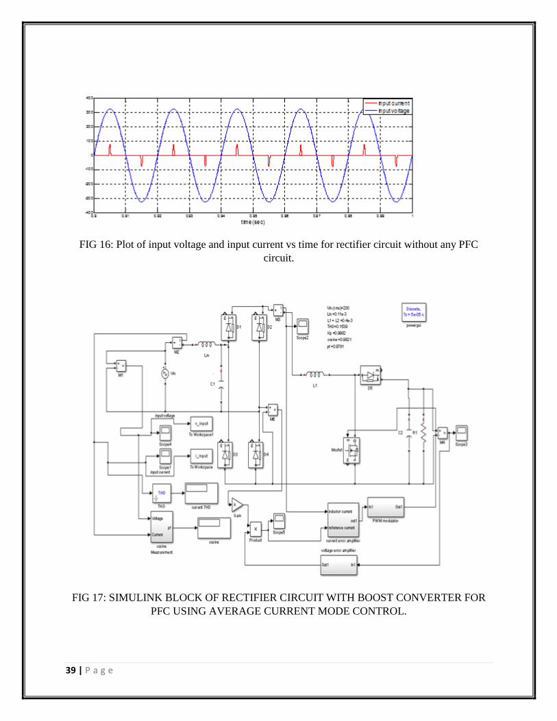
39 | P a g e
FIG 16: Plot of input voltage and input current vs time for rectifier circuit without any PFC
circuit.
FIG 17: SIMULINK BLOCK OF RECTIFIER CIRCUIT WITH BOOST CONVERTER FOR
PFC USING AVERAGE CURRENT MODE CONTROL.

40 | P a g e
FIG 18: Plot of input current vs time for a rectifier circuit with Boost converter as PFC circuit
using average current mode control method.
FIG 19: Plot of input voltage and input current vs time for rectifier circuit with Boost converter
as PFC circuit using average current mode control method.
FIG 20: Output voltage for a rectifier circuit with Boost converter as PFC using average current
mode control method.

41 | P a g e
6.2: RECTIFIER CIRCUIT MODEL WITH PARALLEL BOOST
CONVERTER
FIG 21: SIMULINK BLOCK FOR RECTIFIER CIRCUIT WITH PARALLEL BOOST
CONVERTER.
FIG 22: Plot of input current vs time for a rectifier circuit with parallel Boost converter.

42 | P a g e
FIG 23: Plot of input voltage and input current vs time for rectifier circuit with parallel Boost
converter.
FIG 24 Output voltage for a rectifier circuit with parallel Boost converter.
6.3: CALCULATIONS
(a): RECTIFIER CIRCUIT WITHOUT ANY PFC CIRCUIT.
THD=0.975
Cosine=O.9884
Kp=0.7158
Power Factor=0.7074

43 | P a g e
(b): RECTIFIER CIRCUIT WITH BOOST CONVERTER FOR PFC
THD=0.1539
Cosine=0.9821
Kp=0.9982
Power Factor=0.9781
(c): RECTIFIER CIRCUIT WITH A PARALLEL BOOST CONVERTER FOR PFC
THD=0.1138
Cosine=0.9967
Kp=0.9935
Power Factor=0.9903

44 | P a g e
CONCLUSION
The main objective of my project was to improve the power factor with reduction of harmonics.
The initial simulation started with the simulation of a simple rectifier circuit without using any
control circuits or EMI filters. And this was followed by the simulation of rectifier circuit using
control circuit based on average current mode control method. The current waveforms, power
factor and THD was changed and was recorded accordingly. And later on a PFC circuit in which
two Boost converters were connected in parallel and simulated. And average current mode control
method was used as it keeps a close track with the input current program. Finally to make sure of
improved Power Factor and Total Harmonic Distortion (THD), these parameters from three
different circuits were calculated and compared.
By modelling the Boost converter using ACMC method, THD was recorded 0.1538 and by
modelling Boost converters which were connected in parallel and using ACMC method, the power
factor was improved with improved THD of 0.1137. The second Boost converter which is
connected in parallel to its counterpart filters, the harmonics and the current quality were improved.

45 | P a g e
REFERENCES
[1] Ms. Kurma Sai Mallika,”Topological Issues in Single Phase Power Factor Correction”,
Thesis, Degree of Master of technology In Power control and drives, Department of electrical
engineering National institute of technology Rourkela- 769008, 2007.
[2] Fairchild Semiconductor- “Application Note 42047,Power Factor Correction (PFC) Basics” –
www.fairchildsemi.com
[3] Rashid M., Power Electronics Handbook.
[4] Yiqing Zhao, “single phase power factor correction circuit with wide output voltage range”,
Thesis, Degree of Master of Science, Electrical Engineering, Fred C. Lee, Chairman, Dusan
Borojevic, Dan Y. Chen, February 6, 1998, Blacksburg, Virginia
[5] Rossetto, L., et el. “Control techniques for power factor correction converters.” University of
Padova, Via Gradenigo 6/a, 35131 Padova – ITALY. (1994): pp. 1-9.
[6] Redl, Richard, “Reducing distortion in peak-current-controlled boost power factor correctors.”
Proc. of IEEE Applied Power Electronics Conference, APEC’94. (1994): pp. 576-583.
[7] Maksimovic, Dragan, “Design of the clamped-current high-power-factor boost rectifier.” IEEE
Trans. on Industry Applications. vol. 31, no. 5, (Sept - Oct. 1995): pp. 986-992.
[8] Canesin, Carlos A., et el. “Analysis and design of constant-frequency peak-current controlled
high power-factor boost rectifier with slope compensation.” Proc. of IEEE Applied Power
Electronics Conference, APEC’96. (1996): pp. 807-813.
[9] Lai, J. S., “Design consideration for Power Factor Correction Boost converter Operating at the
Boundary of Continuous Conduction mode and Discontinuous Conduction mode.” Proc. of IEEE
Applied Power Electronics Conference, APEC’93. (1993): pp. 267-273.
[10] Redl, Richard, et el. “Power-Factor Correction with Interleaved Boost Converters in
Continuous-Inductor-Current Mode.” Proc. of IEEE Applied Power Electronics Conference,
APEC’93. (1993): pp.168-174.
[11] Attaianese, C.; Nardi, V.; Parillo, F.; Tomasso, G.; “ Predictive Control of Parallel Boost
Converters” in Industrial Electronics,2008, IECON 2008, 34th Annual Conference of IEEE.

46 | P a g e
[12] Wu, M. K. W., et el. “A review of EMI problems in switch mode power supply design.”
Journal of Electrical and Electronics Engineering, Australia. vol. 16, nos. 3&4, (1996): pp. 193-
204.