Embed Size (px)
Citation preview

Industrial Electrical Engineering and AutomationLund University, Sweden
Power electronics Solution to examination 2009-12-14
© Namn Namn Föredragstitel
Examination 20091214 1a

© Namn Namn Föredragstitel
Examination 20091214 1b
VVUdc 5662400max Maximum dc voltage
Average dc voltage VVU avedc 54024003_
Margin to maximum voltage 1500V = 934 V

© Namn Namn Föredragstitel
Examination 20091214 1c
Phase current
-500-400-300-200-100
0100200300400500
0 0,002 0,004 0,006 0,008 0,01 0,012 0,014 0,016 0,018 0,02
time [s]
[A]

© Namn Namn Föredragstitel
Examination 20091214 1c cont’d
A
dxxdxxI rmsdiode
1152
)0sin(02
)2sin(112
400
2)2cos(1
122400)(sin400
02.000167.02
00
22
AdxxdxxIavediode
4.42cos0cos3200)sin(
3200)sin(400
02.000167.02
00
Rectifier diode rms-current
Rectifier diode average current

© Namn Namn Föredragstitel
Examination 20091214 1c cont’d
Rectifier diode Threshold voltage 0.95 V Differential resistance 2.5 mohm Irms 115 A Average current 42,4 A
WIRIVP rmsdiffavethresholddioderectifier 7.731150025.04.4295.0 22 Rectifier diode power loss

© Namn Namn Föredragstitel
Examination 20091214 1d
0
0,5
1
1,5
2
2,5
3
0 0,002 0,004 0,006 0,008 0,01 0,012 0,014 0,016 0,018 0,02
AdxxIdc 127cos0cos200)sin(02.0
40000167.06
0
Dc current to the dc link and to the 4QC
Duty cycle 80% IGBT and diode on state current 127/0.8= 159A Conduction percentage of IGBT transistor (incl freewheeling) 80+20/2= 90% Conduction percentage of IGBT diode (when freewheeling) 20/2= 10%
Switching frequency 2,5 kHz
© Namn Namn Föredragstitel
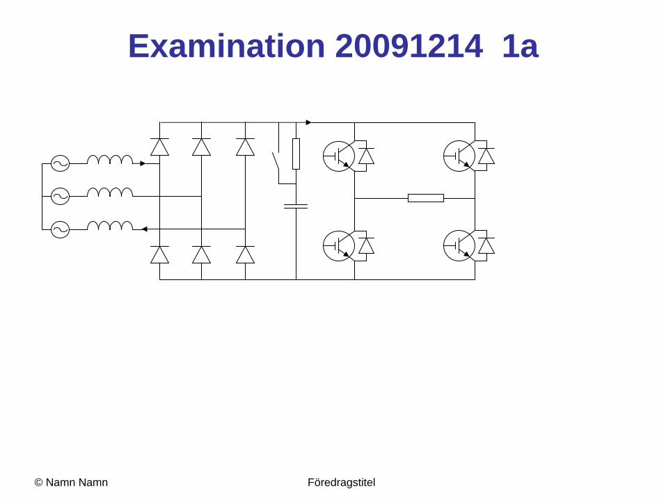
Examination 20091214 1d cont’dIGBT transistor Threshold voltage 1.3 V Differential resistance 15 mohm On state voltage at 159 A 3.68 V Turn on energy at 900 V and 180 A 63 mJ Turn off energy at 900 V and 180 A 80 mJ IGBT diode Threshold voltage 1.05 V
Differential resistance 9.7 mohm On state voltage at 149 A 2.59 V Turn on energy at 900 V and 180 A 0 mJ Turn off energy at 900 V and 180 A 20 mJ Power loss
WP
WP
lossdiode
losstrans
68180900
15954002.025001.015959.2
716180900
159540143.025009.015968.3
_
_

© Namn Namn Föredragstitel
Examination 20091214 1e
Rectifier diode (6) Loss each 73,7W Rth diode 0.13 K/W Temp diff 9.6 deg
IGBT transistor (2) Loss each 716 W Rth trans 0.069 K/W Temp diff 49 deg
Heatsink Contribution fron 6 rectifier diodes and from two IGBT. Ambient temperature 42 deg Total loss to heatsink 6*73,7+2*715+2*68=2008 W Temp diff over heatsink 2008*0.03=60 .2 deg
Junction temperature Rectifier diode 42+60.2+9.6=112 deg IGBT diode 42+60.2+17=119 deg IGBT transistor 42+60.2+49=151 deg
IGBT diode (2) Loss each 68 W Rth diode 0.25 K/W Temp diff 17 deg
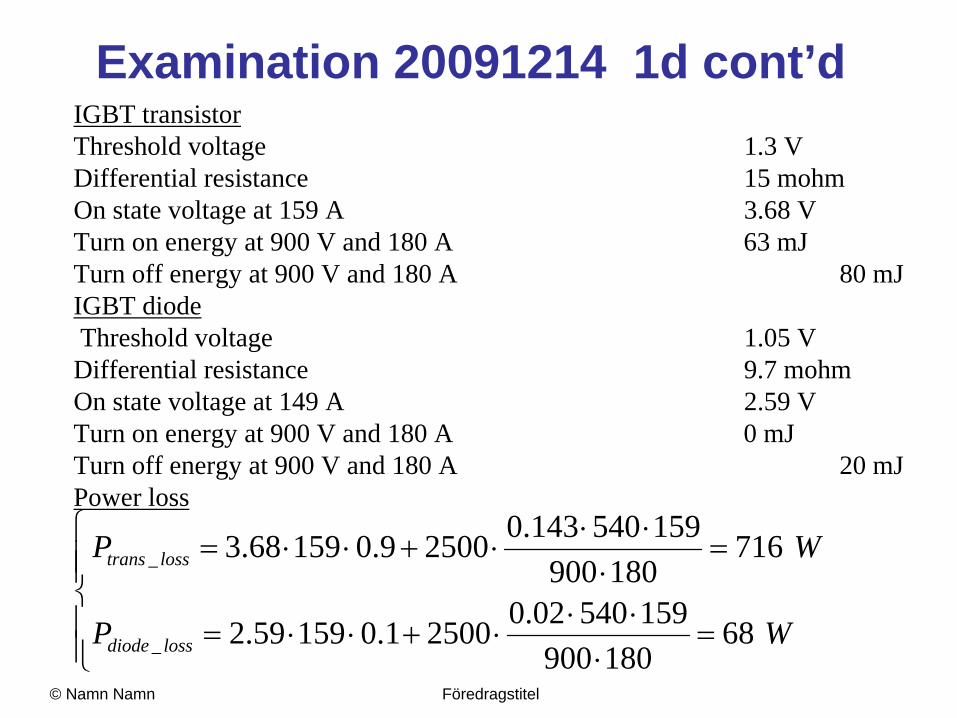
Examination 20091214 2a The buck converter, ”step down chopper”
Vload
VDc

Examination 20091214 2b The buck converter with RCD snubber
D R
C
T
FD
i
At turn off of transistor T, the current i commtutates over to the capacitor C via diode D. The capacitor C charges until the potential of the transistor emitter reduces till the diode FD becomes forward biased and thereafter the load current iload flows through diode FD and the current i=0. A turn on of the transistor T, the capacitor C is discharged via the the transistor T and resistor R. The diode FD becomes reverse biased and the current i commutates to the transistor T.
iload

Examination 20091214 2c Fly-back converter with snubbers and
common mode (CM) and differential mode (DM) filter
vD
DM-filter CM-filter
double voltage

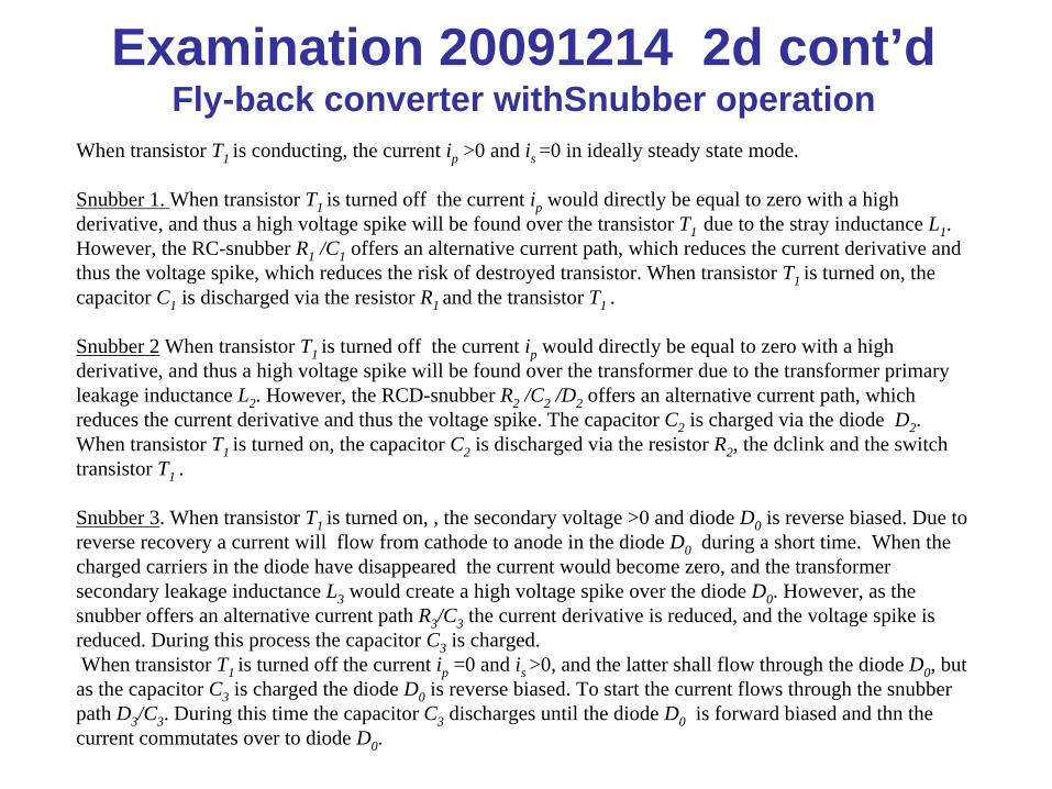
Examination 20091214 2d Fly-back converter withSnubber operation
L1
C1
D2
R1
L2
C2
R2
T1
D3
L3
C3
R3
D0
ip is
For the description of the snubber operation the stray inductance L1 between the switch transistor and the supply/dclink, and the transformer leakage inductance, L2 on primary side and L3 on secondary side are added as discrete component in the circuit drawing above.
Examination 20091214 2d cont’d Fly-back converter withSnubber operation
When transistor T1 is conducting, the current ip >0 and is =0 in ideally steady state mode.
Snubber 1. When transistor T1 is turned off the current ip would directly be equal to zero with a high derivative, and thus a high voltage spike will be found over the transistor T1 due to the stray inductance L1 . However, the RC-snubber R1 /C1 offers an alternative current path, which reduces the current derivative and thus the voltage spike, which reduces the risk of destroyed transistor. When transistor T1 is turned on, the capacitor C1 is discharged via the resistor R1 and the transistor T1 .
Snubber 2 When transistor T1 is turned off the current ip would directly be equal to zero with a high derivative, and thus a high voltage spike will be found over the transformer due to the transformer primary leakage inductance L2 . However, the RCD-snubber R2 /C2 /D2 offers an alternative current path, which reduces the current derivative and thus the voltage spike. The capacitor C2 is charged via the diode D2 . When transistor T1 is turned on, the capacitor C2 is discharged via the resistor R2 , the dclink and the switch transistor T1 .
Snubber 3. When transistor T1 is turned on, , the secondary voltage >0 and diode D0 is reverse biased. Due to reverse recovery a current will flow from cathode to anode in the diode D0 during a short time. When the charged carriers in the diode have disappeared the current would become zero, and the transformer secondary leakage inductance L3 would create a high voltage spike over the diode D0 . However, as the snubber offers an alternative current path R3 /C3 the current derivative is reduced, and the voltage spike is reduced. During this process the capacitor C3 is charged. When transistor T1 is turned off the current ip =0 and is >0, and the latter shall flow through the diode D0 , but as the capacitor C3 is charged the diode D0 is reverse biased. To start the current flows through the snubber path D3 /C3 . During this time the capacitor C3 discharges until the diode D0 is forward biased and thn the current commutates over to diode D0 .

Examination 20091214 2e The MOSFET diffusion layer
Source
Drain
Gate
p n+
body
n+ p
body
n- drift region

© Namn Namn Föredragstitel
Examination 20091214 2f
The drift region, doped n-

Examination 20091214 3a, 3b The buck converter as battery charger
400 V, 11 kW -> I=27.5 A ripple current 4.1 A
540 VL I
Switching frequency 2 kHz Period time 0.5 msDuty cycle withj 27.5 A =0.79 On pulse 0.5 *0.79=0.395 ms
mHLLdtdiLUb 11
1.4000395.05.112
000395.01.45.4275403
R

Examination 20091214 3c The buck converter as battery charger
Assume resistance=1 ohm Phase voltage with 0 A=400 Vdc Duty cycle with 0 A=0.74On pulse 0.5 *0.74=0.37 msRise di/dt with 0 A (540-400)/0.011=12.7Fall di/dt with 0 A -400/0.011=-36.4
Current step to 13.75 APhase voltage with 13.75 A=413.75 V Duty cycle with 13.75 A=0.77 On pulse 0.5 *0.77=0.385 msRise di/dt with 13.75 A (540-4 13.75)/0.011=11.5Fall di/dt with 0 A -4 13.75 /0.011=-37.6

© Namn Namn Föredragstitel
Examination 20091214 4a
)3
4(ˆ
)3
2(ˆ
)(ˆ
tCOSee
tCOSee
tCOSee
c
b
a
tj
tj
j
c
j
ba
eE
eetjte
jttejjtjjte
jttjttte
jttjttte
jtjtteeeeeee
23ˆsincos
23ˆ
23sin
23cos
32ˆ
43
43
43
43sin
43
41
43
411cos
32ˆ
23
21
23sin
21cos
23
21
23sin
21coscos
32ˆ
23
21
34sinsin
34coscos
23
21
32sinsin
32coscoscos
32ˆ
23
21
34cos
23
21
32coscos
32ˆ
32 3
43
2

© Namn Namn Föredragstitel
Examination 20091214 4b
< a/b/c vect
d/q >
d-comp vect q-comp angle
>a/b/cid PI-controller ref act emf
3-phase modulator
3-phase inverter
Ts/2-advance
> d/qVect angle
> d/qVect angle
Flux-angleFlux emf
angle
-1
iq PI-controller ref act emf
3-phase current measurement
e e e
3-phase load
udclink
i*
iact
psi

© Namn Namn Föredragstitel
Examination 20091214 5
NmPTorque
NmPTPTorquee
HzfreqElecfreqswitchingleastatHzfreqElecfreqswitchingleastatd
HzfreqsampingperiodfreqpertwiceSamplecHzpolesfreqElec
HzfreqMechc
AIIassumeb
VUVamplitudevoltagePhasea
rpm
rpm
linetolinerms
8.39
60120002
50000
119
6040002
500005
5400.31800.5
36005180018.
20060
120005
1059.03063
500009.030639.0cos500005
30632
2502502
5005
12000
4000
___