Embed Size (px)
Citation preview
SemiSouth Laboratories, [email protected]
www.semisouth.com201 Research Blvd.Starkville, MS 39759
662-324-7607

Power Electronicsfor High Tech Inverters
Michael S. Mazzola, Ph.D., P.E.
SemiSouth Laboratories, Inc.and
Center for Advanced Vehicular Systems,Mississippi State University

Outline
• Introduction– Components in inverters– Power component R&D
• Silicon Carbide Power Electronics– System Benefits– Capabilities– Trends

Introduction
Components in Inverters

3535
3030
2525
2020
1515
1010
55
00
Cap
acito
rs
Bus
Wor
k
PWBs
Mag
netic
s
Ther
mal
Mgm
t.
Cur
rent
Sen
sors
Con
tact
ors
ALL INVERTERS, CONVERTERS AND MOTOR CONTROLLERSCONSIST OF . . . . . . . . . .
Solid
Sta
te S
witc
hes For 10 – 250kW
Systems
% WEIGHT % VOLUMECourtesy of Dr. James Scofield, Propulsion Directorate, Air Force Research Laboratory, Wright-Patterson Air Force Base

270 VDC
To Motor
Flight Packaged Motor Drive
Typical Inverter Topology
• Six-pulse topology. • Switches are typically IGBT’s or MOSFET’s• Each switch has an integral anti-parallel rectifier.
• Six-pulse topology. • Switches are typically IGBT’s or MOSFET’s• Each switch has an integral anti-parallel rectifier.
Courtesy of Dr. James Scofield, Propulsion Directorate, Air Force Research Laboratory, Wright-Patterson Air Force Base

Applications Driver – Power Density
• Much of the cumulative improvement in power density is still in the future (Moore’s law for power?).
• Civilian transportation and communication applications will drive much of the technology development (affordable).
• The ultimate is goal is monolithically manufactured power supplies.
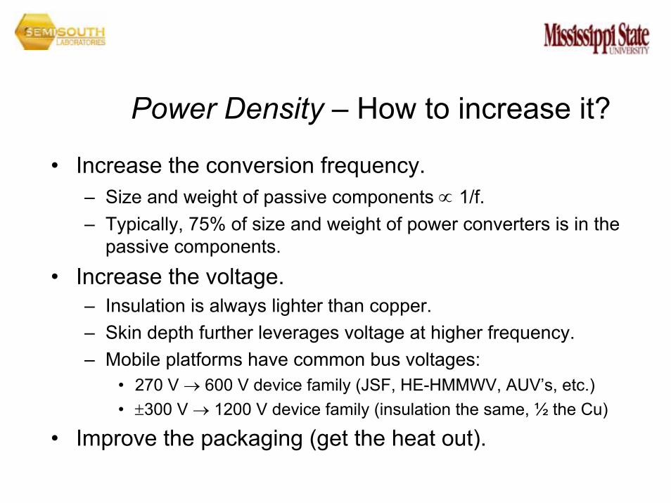
Power Density – How to increase it?
• Increase the conversion frequency.– Size and weight of passive components ∝ 1/f.– Typically, 75% of size and weight of power converters is in the
passive components.
• Increase the voltage.– Insulation is always lighter than copper.– Skin depth further leverages voltage at higher frequency.– Mobile platforms have common bus voltages:
• 270 V → 600 V device family (JSF, HE-HMMWV, AUV’s, etc.)• ±300 V → 1200 V device family (insulation the same, ½ the Cu)
• Improve the packaging (get the heat out).
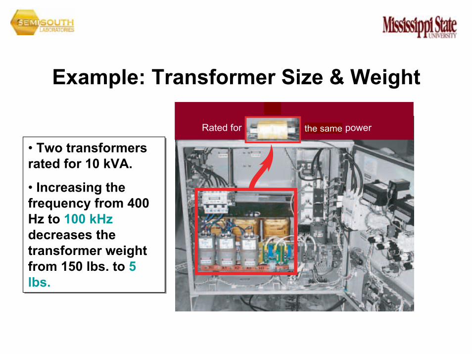
Example: Transformer Size & Weight
• Two transformers rated for 10 kVA.
• Increasing the frequency from 400 Hz to 100 kHzdecreases the transformer weight from 150 lbs. to 5 lbs.
• Two transformers rated for 10 kVA.
• Increasing the frequency from 400 Hz to 100 kHzdecreases the transformer weight from 150 lbs. to 5 lbs.
twice the powerRated for
2Xthe same

Why is an anti-parallel diode needed?
• Bidirectional power flow for dc-ac inverters.– Supplying reactive power.– Conducting harmonic currents.
• Energy recovery in motor drives.– Recover energy stored in parasitic inductances.– PWM in Brushless DC (BLDC) motor drives.
• Conducting resonant currents in soft-switched power supplies and drives.– To continue increasing conversion frequency, minimizing
inductance between switch and anti-parallel diode is essential.– Lowest possible inductance is achieved monolithically.
2
1

Anti-parallel current paths: Two possibilitiesHard-Switched BLDC
Motor DriveHard-Switched BLDC
Motor Drive
+ 300 V
- 300 V
Motor Winding
Motor Current
time
Ave.
Half Bridge
• Switch & Diode work on opposite legs.• Switch & Diode work on opposite legs.
• Switch & Diode work on the same leg.• Switch & Diode work on the same leg.
Inductor Current
time
+ 300 V
- 300 V
Half Bridge
Soft-Switched Resonant Power Supply
Soft-Switched Resonant Power Supply
L r Cr
ZCS
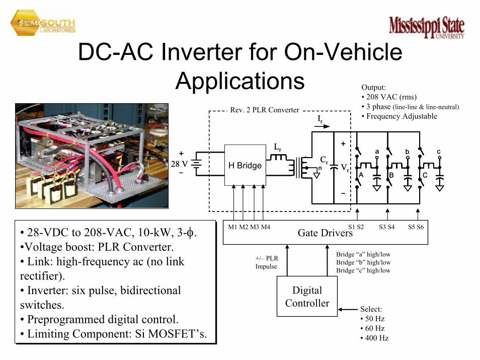
DC-AC Inverter for On-Vehicle Applications
H Bridge
a b c
Vr
+
Ir
Cr
Lr
28 V+
Rev. 2 PLR Converter
nA B C
H Bridge
a b c
Vr
+
Ir
Cr
Lr
28 V+
Rev. 2 PLR Converter
nA B C
Digital Controller Select:
• 50 Hz• 60 Hz• 400 Hz
Gate Drivers
+/– PLRImpulse
Bridge “a” high/lowBridge “b” high/lowBridge “c” high/low
M1 M2 M3 M4 S1 S2 S3 S4 S5 S6• 28-VDC to 208-VAC, 10-kW, 3-φ.•Voltage boost: PLR Converter.• Link: high-frequency ac (no link rectifier).• Inverter: six pulse, bidirectional switches.• Preprogrammed digital control.• Limiting Component: Si MOSFET’s.
• 28-VDC to 208-VAC, 10-kW, 3-φ.•Voltage boost: PLR Converter.• Link: high-frequency ac (no link rectifier).• Inverter: six pulse, bidirectional switches.• Preprogrammed digital control.• Limiting Component: Si MOSFET’s.
Output:• 208 VAC (rms)• 3 phase (line-line & line-neutral)• Frequency Adjustable

The PLR Voltage Pulse in an AC-Link Inverter
time+δ(t)
–δ(t)
r
pVdtt
ωδ
4)(Area == ∫
Vr(t) = Vp sin[(ωr /2)t ]
time
ωr
2πωs
2π
Vr(t) = Vp sin[(ωr /2)t ]
time
ωr
2πωr
2πωr
2πωs
2πωs
2πωs
2π
r
pVω
4Area =Vr(t)
PLR Converter Voltage Waveforms
Impulse Function Model of Resonant Capacitor Voltage
Sine Function Model of Resonant Capacitor Voltage
Components are stressed by resonant voltages and currents well in excess
of inverter terminal ratings.
Components are stressed by resonant voltages and currents well in excess
of inverter terminal ratings.
Peak Inverter MOSFET Stress > 800 V.MOSFET RMS Current = 28 A.
Peak Inverter MOSFET Stress > 800 V.MOSFET RMS Current = 28 A.

Introduction
Power Component Research & Development
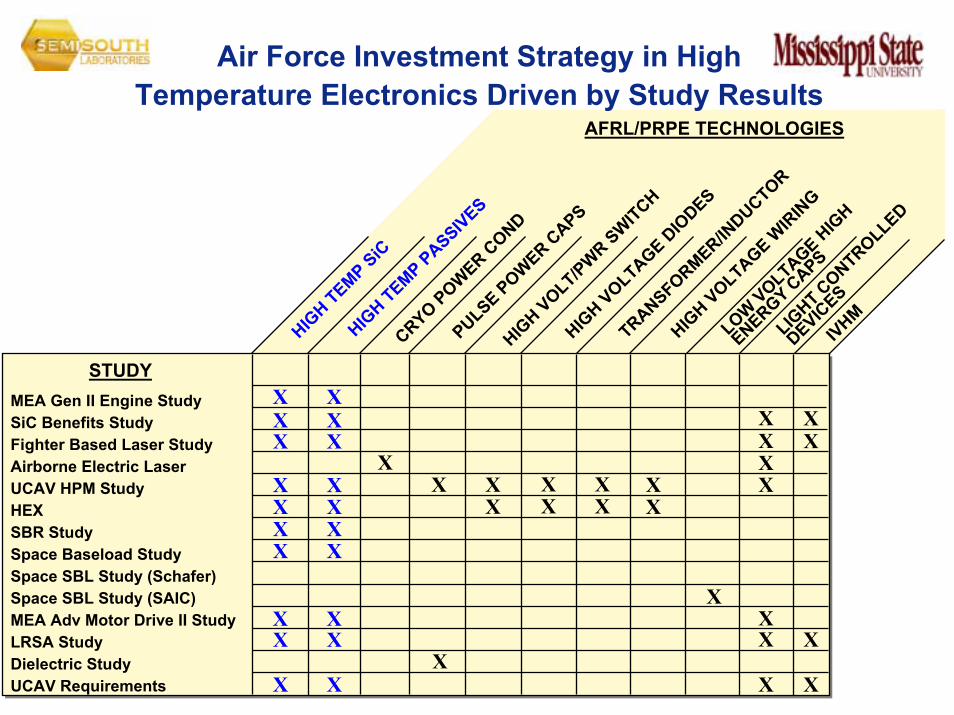
MEA Gen II Engine StudySiC Benefits StudyFighter Based Laser StudyAirborne Electric LaserUCAV HPM StudyHEXSBR StudySpace Baseload StudySpace SBL Study (Schafer)Space SBL Study (SAIC)MEA Adv Motor Drive II StudyLRSA StudyDielectric StudyUCAV Requirements
TRANSFORMER/INDUCTOR
HIGH TEMP SiC
HIGH TEMP PASSIVES
CRYO POWER COND
PULSE POWER CAPS
HIGH VOLT/PWR SWITCH
HIGH VOLTAGE D
IODES
AFRL/PRPE TECHNOLOGIES
STUDY
LOW VOLTAGE HIG
H
ENERGY CAPS
HIGH VOLTAGE W
IRIN
G
Air Force Investment Strategy in HighTemperature Electronics Driven by Study Results
LIGHT C
ONTROLLED
DEVICES
X XX XX X
XX X X X X X X X
XXX
X X X X X XX XX X
X X XX
IVHM
X X
X XX
X
X
XX
X
X
What is Silicon Carbide?Silicon forms a stronger chemical bond to carbon than to silicon!
SiC is very hard (third hardest substance known)SiC handles very high temperatures (wafers are made at over 3600°F)SiC handles very high voltages (ten times that of silicon and gallium arsenide)
Single crystal SiC wafers for electronics use commercially available:1990 - 1 inch diameter2003 – 3 inch diameter2006(?) – 4 inch diameter
Early versions of SiC power devices perform better than the bestperforming silicon power devices.
SiC power products are commercially available and in commercial use.

Motivation to DevelopSiC Power Devices
Silicon vs. Silicon CarbidePower Semiconductors
PROPERTY SILICONSILICONCARBIDE
BANDGAP (eV@ 300K)
MAXIMUM OPERATINGTEMPERATURE (K)
BREAKDOWN VOLTAGE(106 V/cm)
THERMAL CONDUCTIVITY(W/cm - °C)
PROCESS MATURITY
INTRINSICALLY RAD HARD
1.1
425
0.3
1.5
HIGH
NO
2.9
>900
4
5
LOW
YES
SiC Power Electronics
System Benefits

Overview of BenefitsLower On-resistance increased system efficiency
Higher Frequency smaller power supplies
Higher Temperature relaxed cooling requirements
Payoff: Improved System Performance
(size, weight, cost, reliability, efficiency)
Current commercial applications
1. High-end server power supplies: improved efficiency means smaller supply with the same or less heat generation
Potential future SiC power switch applications
1. High-temperature motor drives & inverters.2. High-power-density resonant inverters with high voltage stress.

Obstacles to increasing Power Density• Simultaneous increases in voltage and frequency limited by
silicon – Efficiency cannot be compromised!– MOSFET silicon switches are fast but not voltage scalable.
– IGBT’s voltage scalable, but not as fast (∼ 20 kHz).
– Reverse recovery of anti-parallel diode another limitation.
• Parasitic inductances and capacitances require resonant circuits (“soft switching”) above 100 kHz and 1-10 kW.– Soft switching requires teaming fast switches with ultra fast
anti-parallel diodes.
• VJFET is the best available >1 MHz, 600-1800 V SiC switch.– “Normally on” and “Normally off” available
– Has the best possible anti-parallel diode: a SBD

Weight VolumeSavings (lbs) Redn.(in3)
Flight Control EHAs/EMAs 58.5 1,350Utility Control Actuators 15.4 313EPS Equipment 45.1 657Avionics 17.6 245ECS/Fuel/Misc Motors 10.9 252TMS Equipment 30+ 400+
Total 177.5+ 3,217+
MEA F/A-18MEA F/A-18
Vehicle-Level SiC Benefits
Minimum 177 lb Equipment Weight and 3,210 in3 Equipment Volume Savings.

SiC Power Electronics
Capabilities

Candidates for SiC Switches• SiC MOSFET
– Unipolar – Normally off– p-n body diode
• Always present
– Low channel mobility– Oxide reliability issues
• SiC JFET– Unipolar– Normally on
• Normally off and “quasi-on” options
– No body diode– Not as sensitive to
oxide interface and reliability issues

4H-SiC Vertical JFETBasic device cross-section
Finished JFET in a TO-257
SiO2
source contact
drain contact
SiO2
source contact
drain contact
n+
implantedp-type gate
n-type substrate
n- drift

VJFET Technology
SemiSouth 600V SiCFET
0
5
10
15
20
25
0 5 10 15 20Drain Voltage (V)
Dra
in C
urre
nt (A
)
Vg=0Vg=1Vg=2vg=-10
• Hard Switch @ 20MHz• Tjmax ≥ 300 °C• Parallel multiple die for
high total current
Multi-die package600V, 20A
Sept 2003
ron = 6.8 mΩ*cm2
Parts currently being sampled to customersMonitored by Dr. J. Scofield, WPAFB
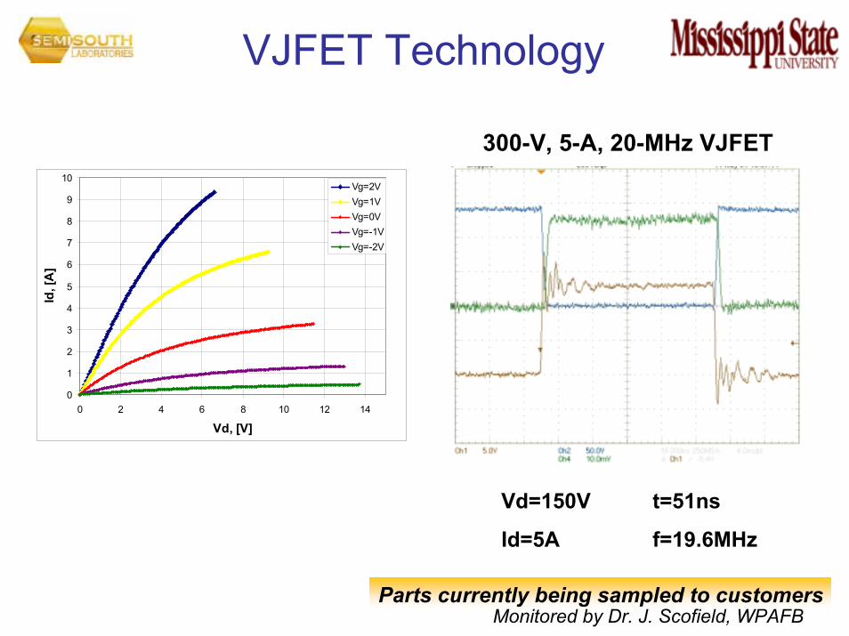
VJFET Technology
300-V, 5-A, 20-MHz VJFET
0
1
2
3
4
5
6
7
8
9
10
0 2 4 6 8 10 12 14
Vd, [V]
Id, [
A]
Vg=2VVg=1VVg=0VVg=-1VVg=-2V
Vd=150V
Id=5A
t=51ns
f=19.6MHz
Parts currently being sampled to customersMonitored by Dr. J. Scofield, WPAFB

The “Quasi-on” OptionNormally on: VT is negative.Normally off: VT is positive.
Quasi-on: VT is slightly negative
VDS = 10V
1.E-12
1.E-10
1.E-08
1.E-06
1.E-04
1.E-02
1.E+00
-10 -9 -8 -7 -6 -5 -4 -3 -2 -1 0 1VGS (V)
I DS (A
) normally on
quasi-on
normally off
10-10
10- 12
10- 8
100
10- 6
10- 2
10- 4
VDS = 10V
0
0.2
0.4
0.6
0.8
1
-5 -4 -3 -2 -1 0 1VGS (V)
I DS
(A) normally on
quasi-on
normally off

Benefits of a Quasi-on JFET• Improved blocking• Circuit protection
• Acceptable current trade-off
1.73 A
0.24 A
0
0.5
1
1.5
2
0 2 4 6 8 10VDS (V)
I DS (A
)
normally on
quasi-on
VGS = 0 V
VGS = -10 V
1.E-10
1.E-09
1.E-08
1.E-07
1.E-06
1.E-05
1.E-04
0 100 200 300 400 500 600VDS (V)
I DS (A
)
normally on
quasi-on
10-10
10- 9
10- 8
10-7
10- 6
10- 5
10- 4
3.5 A
2.6 A
0
0.5
1
1.5
2
2.5
3
3.5
4
0 2 4 6 8 10VDS (V)
I DS (A
)
normally on
quasi-on
VGS = 2 V

DC Characteristics at ElevatedTemperatures
DC IDS at VDS = 10 V as a function of temperature for a 600V 4H-SiC VJFET
DC IDS vs. VDS at VG = -10 V for temperatures up to 250ºC 4H-SiC VJFET
VGS = -10 V
1. E- 10
1. E- 0 9
1. E- 0 8
1. E- 0 7
1. E- 0 6
1. E- 0 5
1. E- 0 4
0 100 200 300 400 500 600VDS (V)
I DS (A
)
250ºC200ºC150ºC100ºC25ºC
10-10
10- 9
10- 8
10-7
10- 6
10- 5
10- 4
VDS = 10 V
0
0.5
1
1.5
2
2.5
3
0 50 100 150 200 250 300T (ºC)
I DS (A
)
2 1.5 1 0.5 0
VGS (V)

Summary
• The 600V SiC VJFETs had typical ron values from 6.5 to 10 mΩ*cm2 at room temperature.
• Devices exhibited an expected decrease in drain current with increasing temperature with IDS at 300ºC = ~ 30% IDS at 25ºC.
• Early generation VJFET had maximum switching frequencies in the MHz range which increased with temperature.
• Next generation VJFET has much reduced gate resistance and RT switching over 20 MHz.
SiC Power Electronics
Trends

SiC VJFET/Diode in DC-DC Buck Converter (VJFET @ 225°C)
Comparison of SiC switch (specific on-resistance)
Blocking Voltage\
InfineonSi switch
InfineonVJFET-A
InfineonVJFET-B
SemiSouth
VJFET
600 V 30 (COOLMOS™)
8 20 6.8
1200 V 400 + 12 22
1800 V NA 14 24
Improving SiC Power Switches
MDA/AFRL Program produced a patented SiC VJFET switch which has:
Lower on-resistanceSimpler (inexpensive) fabrication processLower packaging costs

Increased Requirements forHigh Temperature Electronics
• Near Term (3 - 5 years)– 250°C - 300°C (max) junction temperature– Reduction in requirements for active cooling
• Far Term (5 - 9 years)– 300°C - 350°C (max) junction temperature– Supports “high speed” aircraft

SemiSouth and SiC is in the Commercial Market Place
Epitaxy
SiC MaterialsQuality Control
Power Switch
SiC Devices Power Rectifier
RF Transistor
Device Design
SiC OEMDevice Fabrication

Multiple Sources, Decreasing PricesCree II-VI SemiSouth Dow Corning
Substrates Substrates Substrates↓ ↓
Epi Epi Epi↓ ↓
Devices Devices↓ ↓
End users, VARs End users, VARs“Virtual” Vertical Integration
Provide true direct alternative to CreeBut, provides insulation from competing with customers
Open source of SiC technology – provide industry with true 2nd or alternate source… something many customers want now.
Provides direct market feedback and drive to emerging 4H epi-wafer market.