Embed Size (px)
Citation preview
POWER CONVERTERS98% Efficient Single-StageAC/DC Converter Topologies
ISSUE 4 – June 2011 www.power-mag.com
Also inside this issueOpinion | Market News | PCIM 2011 | Power Semiconductors | Solar Power | Thermal Management | Products | Website Locator |
01_PEE_0411_p01 Cover 15/06/2011 12:03 Page 1

02_PEE_0411_02_PEE_0411 15/06/2011 11:41 Page 1

CONTENTS
Power Electronics Europe Issue 4 2011 www.power-mag.com
3
Editor Achim Scharf
Tel: +49 (0)892865 9794
Fax: +49 (0)892800 132
Email: [email protected]
Production Editor Chris Davis
Tel: +44 (0)1732 370340
Financial Clare Jackson
Tel: +44 (0)1732 370340
Fax: +44 (0)1732 360034
Circulation Manager Anne Backers
Tel: +44 (0)208 647 3133
Fax: +44 (0)208 669 8013
Email: [email protected]
INTERNATIONAL SALES OFFICES
Mainland Europe:
Victoria Hufmann, Norbert Hufmann
Tel: +49 911 9397 643 Fax: +49 911 9397 6459
Email: [email protected]
Armin Wezel
Tel: +49 9568 897 097 Fax: +49 9568 897 096
Email: [email protected]
UK
Steve Regnier, Tim Anstee
Tel: +44 (0)1732 366555
email: [email protected]
Eastern US
Karen C Smith-Kernc
email: [email protected]
Western US and Canada
Alan A Kernc
Tel: +1 717 397 7100
Fax: +1 717 397 7800
email: [email protected]
Italy
Ferruccio Silvera
Tel: +39 022 846 716 Email: [email protected]
Taiwan
Prisco Ind. Service Corp.
Tel: 886 2 2322 5266 Fax: 886 2 2322 2205
Publisher Ian Atkinson
Tel: +44 (0)1732 370340
Fax: +44 (0)1732 360034
Email: [email protected]
www.power-mag.com
Circulation and subscription: Power ElectronicsEurope is available for the following subscriptioncharges. Power Electronics Europe: annual chargeUK/NI £60, overseas $130, EUR 120; single copiesUK/NI £10, overseas US$32, EUR 25. Contact: DFA Media, Cape House, 60a Priory Road, Tonbridge,Kent TN9 2BL Great Britain. Tel: +44 (0)1732 370340. Fax: +44 (0)1732360034. Refunds on cancelled subscriptions willonly be provided at the Publisher’s discretion, unlessspecifically guaranteed within the terms ofsubscription offer. Editorial information should be sent to The Editor,Power Electronics Europe, PO Box 340131, 80098Munich, Germany. The contents of Power Electronics Europe aresubject to reproduction in information storage andretrieval systems. All rights reserved. No part of thispublication may be reproduced in any form or by anymeans, electronic or mechanical includingphotocopying, recording or any information storageor retrieval system without the express prior writtenconsent of the publisher.Printed by: Garnett Dickinson.ISSN 1748-3530
PAGE 10
PCIM 2011PCIM 2011 from May 17 - 19 attracted more than 730 conference delegates
(2010: 619), 6600 exhibition visitors and 298 exhibitors with additionally 67
represented companies. With these figures PCIM is growing from year to year
(20% in exhibitors, ) and among the largest power electronic events worldwide.
PCIM Europe 2012 will take place from May 8 - 10 again in Nuremberg.
PAGE 25
Gallium Nitride for 600VOperationEspecially for mains voltage applications, new efficient 600V class devices are
required. These devices are within the main product focus of MicroGaN, as
outlined at PCIM. Two basic elements are developed which will enable the layout
of all required power circuits: the power diode and the power switch. Additionally,
a unique fabrication technology has been developed to reduce chip area, chip
price and device parasitics as well as providing compatibility to standard PCB to be
competitive on the market. Ertugrul Sönmez, Ulrich Heinle, Mike Kunze, and
Ingo Daumiller, MicroGaN, Ulm, Germany
PAGE 29
New SiC JFET Boost Performanceof Solar InvertersThe article proposes a new normally-on Silicon Carbide (SiC) JFET device concept
with monolithically integrated body diode. The new device combines ultra fast
switching with ohmic forward characteristic and a zero reverse recovery
characteristic of its body diode. It allows a significant boost of the performance of
solar inverters especially in the light of new requirements such as reactive power
capability and fault ride through. Best device performance is achieved with a direct
driven approach, compatible with safety aspects in voltage driven topologies
which is implemented in combination with a low voltage MOSFET.
Gerald Deboy, Roland Rupp, Infineon Technologies Austria/Germany,
and Regine Mallwitz, Holger Ludwig, SMA Solar Technology, Germany
PAGE 34
Efficient LED Heat ManagementLEDs are being used in more and more ways. Due to their brightness, high
efficiency and long life expectancy, they continue to conquer domains that only
recently were reserved for traditional light sources. This means that driver
electronics must be adapted to an ever-increasing number of applications.
Markus Eißner, Ingenieurbüro Eissner for Kerafol, Eschenbach, Germany
PAGE 36
Product UpdateA digest of the latest innovations and new product launches
PAGE 41
Website Product Locator
98% Efficient Single-Stage AC/DCConverterTopologiesThe goal of developing AC/DC converters withIsolation and Power Factor Correction (PFC) feature ina single power processing stage and without amandatory full-bridge rectifier has for years eludedpower electronics researchers (see Figure 1). PresentAC/DC converters operated from a single-phase ACline are based on conventional Pulse WidthModulation (PWM) switching method and process thepower through at least three distinct power processingstages: full-bridge rectifier followed by boost PFCconverter and another cascaded isolated full-bridgeDC/DC converter stage, which together use a total of14 switches and three magnetic components resultingin corresponding efficiency, size and cost limitations.
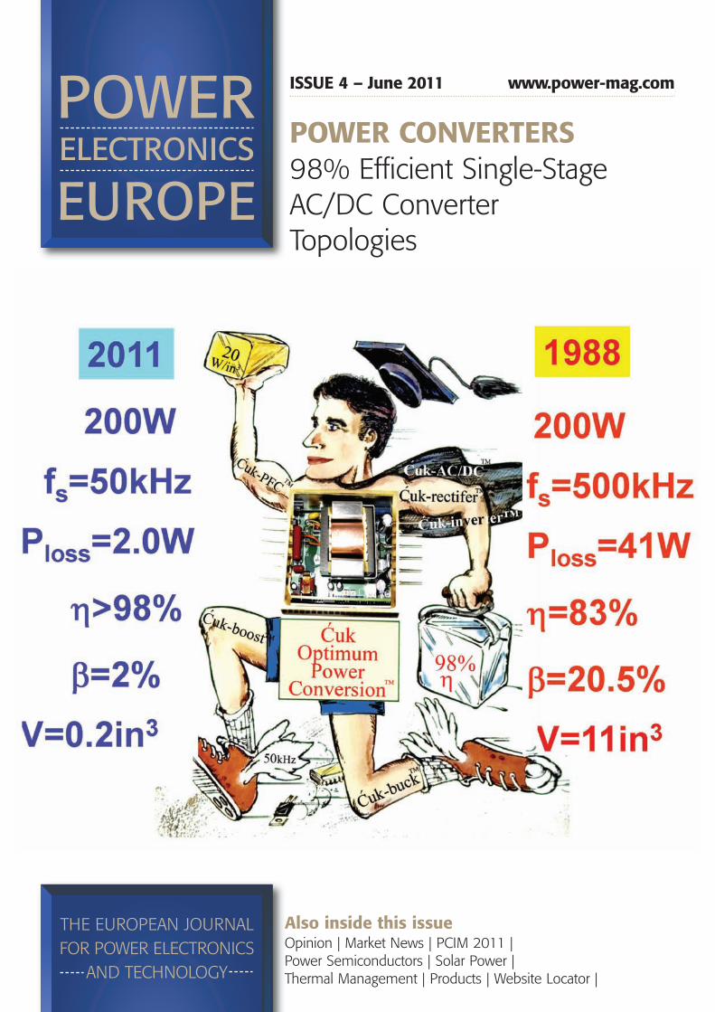
The new Hybrid Switching Method enables newSingle-Stage AC/DC converter topology, the TrueBridgeless PFC Converter consisting of just threeswitches and a single magnetic component albeit at amuch higher efficiency approaching 98% and having a0.999 power factor and 1.7% total harmonicdistortion. Three-Phase Rectifier consisting of threesuch Single-Phase Rectifiers takes for the first time afull advantage of Tesla’s three-phase transmissionsystem to convert constant instantaneous input powerof a three-phase system directly to a constant DCoutput power, albeit isolated at high switchingfrequency, with near unity power factor (0.999), lowtotal harmonic distortion (1.7%), smaller size andlower cost but at ultra high efficiency of 98%. Full storyon page 16
Cover supplied by TESLAco, Irvine, USA
COVER STORY
PAGE 6
Market NewsPEE looks at the latest Market News and company
developments
p03 Contents_p03 Contents 15/06/2011 15:50 Page 3

04_PEE_0411_04_PEE_0411 15/06/2011 11:29 Page 1

OPINION 5
Power Electronics Europe Issue 4 2011 www.power-mag.com
A suitablequote as alead in to
the editorsopinion
The demand for power electronics is set to increase with the increasedusage of electricity. The International Energy Agency anticipates thatglobal energy consumption will increase by over 35% in the next 20years. About one third of the energy used worldwide is consumed in theform of electricity. This electric power is transmitted over long distancesand often a great deal of energy is lost in the process. The intelligentdeployment of power semiconductors counteracts this energy loss byenabling energy to be generated, distributed and converted withminimum loss, particularly with the more widespread use ofregenerative energies such as Wind and Solar Power in the upcomingSmart Grids. One of the sub-segments of the Smart Grid is Electromobility.
Transportation currently accounts for around 4% of electricityconsumption in Germany, all of this is for rail transport, of which 90% iselectrified. Vehicles equipped with internal combustion engines areresponsible for around 20% of total CO2 emissions worldwide. Givenclimate change, however, and the increasing difficulty of tapping theearth’s remaining oil reserves, researchers and also industry confidentlypredict the coming of age of the electric automobile. According toRenault in the year 2020 around 10% of automobile production orseven million will be electric vehicles. Electrical vehicles have really to beconsidered in the global context of electricity production and distribution.Communication between car and infrastructure as well as control of EVcharge through optimized strategies are also key issues in order to takeadvantage as much as possible of a large EV fleet, from a technical pointof view but also from an environmental one. This is also a big challenge,especially in the context of emerging smart grids. For future electric vehicles, new power electronic systems are
required. Here device technologies which can withstand hightemperatures such as GaN and SiC are of great interest, said Renault’sPatrick Bastard in his keynote at PCIM Europe. GaN and SiC can be usedfor the power train, because cost decrease for the power systemincluding cooling efforts justifies the application of these more expensivepower semiconductors. Additionally, to get rid of rare earth materials forelectric motors reluctance motors will be used. Beside low weight and asmall volume, low losses and an excellent dynamic behavior aredemanded. These requirements cannot be met with conventional
converters like 2-level IGBT converters or NPCs. The new Modular HighFrequency-Converter (MHF) introduced by Anna Mayer, University ofFederal Armed Forces, Munich/Germany in her paper “Control Conceptof the Modular High Frequency Converter for Vehicle Applications” whichwas awarded for PCIM’s Young Engineer Award enables essentialimprovements of these problems. Main points are very high efficiency,ultra light weight and “fault ride through” capability. It is especially suitedfor future cars with multi-motor drives and integrated power electronics.For the MHF converter a new control concept, based on the modularconcept of the hardware, was developed. The paper showed the resultsof this concept, including the main points dynamic torque control,disturbance on battery voltage, and continued (redundant) operationafter defects. PCIM’s Best Paper Award has been given to Sebastian Liebig from
Liebherr Electronic (Germany) for his work “Concept and prototyping ofan active mains filter for aerospace application”. This award sponsoredby Power Electronics Europe and SEMIKRON includes a €1000,00 priceand invitation to PCIM China 2012. One major topic in aerospaceapplications is the substitution of hydraulic or pneumatic systems withelectrical systems such as electrical environmental condition system.Conventionally, the DC-link voltage is generated using state-of-the-arttopologies, most commonly active power factor correction orautotransformer rectifier unit. The active parallel power filter representsan interesting alternative to these topologies, since it has to be designedonly for the sum of 5th and 7th harmonic power. The switching of activefilter and motor inverter is translated into a voltage spectrum, whichresults together with impedance matrices in distortion currents. Theinfluence of input and output filters can be calculated by simply addinganother two matrices. The full power prototype is being set up withcustomized SP3-modules from Microsemi using 1700V SiC MOSFETand SiC diode chips (both from Cree). The loss comparison with a1200V NPT-IGBT in an SP3-module reveals that SiC technology leads to64% reduced losses at 60 kHz. Even at 100kHz the MOSFET offers a50% benefit compared to the IGBT at 60kHz. Liebherr Electronic hasinvested €20,000 in this project.This was a direct link to PEE’s Special Session ‘High Frequency
Switching Devices and Applications’, attracting more than 120conference delegates. Thus it was the major session on GaN/SiCtechnologies and devices. Five papers were presented byMicroGaN/Germany, ACOO-IR/USA, Cree/USA, SemiSouth/USA andInfineon-SMA/Austria-Germany. This joint paper presented a newnormally-on SiC JFET with monolithically integrated body diodeincorporated in a solar inverter. The standard solar inverter based onSilicon switches achieves a maximum efficiency of 98.2%. For thecommercial solar inverter equipped with the new SiC JFETs 98.8%system efficiencies can be obtained, SMA pointed out. And this resultwill push solar technology hopefully further, particularly since Germanyhas decided to step out of nuclear power.
Achim ScharfPEE Editor
More Power forRenewables
05_PEE_0411_p05 Opinion 15/06/2011 09:05 Page 5

6 MARKET NEWS
Issue 4 2011 Power Electronics Europe www.power-mag.com
Intersolar Europe presented thelatest Trends in Photovoltaics
At Intersolar Europe in Munich. From June 8-10,2011, around 2,000 companies showcased thelatest trends and developments in solartechnology, with photovoltaics once againoccupying a large part of the exhibition.Faced with the environmental challenges
that go hand in hand with supplying energy toan increasing global population, numerousincentive programs across the globe haveemerged for developing renewable energy -most recently in India and China. At the sametime, the German feed-in tariff is falling.Therefore, researchers and industry are workingagainst the clock to achieve grid parity - thepoint at which electricity from photovoltaicinstallations can be sold at a competitive price. The last 20 years have witnessed some
irrefutable technological advances inphotovoltaics. In 1989, the world record for theefficiency of multicrystalline silicon solar cellsstood at 14.5%. In 2004, this rose to 17.7% andthe 20% mark is already in sight for 2011.Developments in this field are first andforemost thanks to improved productionmethods. For example, improved siliconcrystallization processes in modern plants canalone raise module efficiency by at least 0.4%.In addition to developments in the field ofcrystalline silicon solar cells, an array ofalternative systems, particularly thin-filmtechnologies based on CIS/CIGS, cadmiumtelluride and the new copper zinc tin sulfide(CZTS) is available. The rise in solar module efficiency is
particularly encouraging. As recently asFebruary, researchers at Fraunhofer Institute for
Solar Energy Systems ISE (Freiburg/Germany)posted a new record for the efficiency of large-area, easy-to-manufacture silicon solar cells,reaching 19.3% - these cells could soonemerge on the market. Researchers arepursuing different avenues to increase solar cellefficiency. Selecting optimal silicon materialand developing new innovative productionmethods and technologies both play their rolein boosting efficiency. Such methods includeimproving emitters, for example, which collectthe electric charge carriers. This was also theapproach adopted by researchers at FraunhoferISE, who developed an aluminum-doped
emitter for their record breaking module.Nanotechnology and pioneering laserprocessing techniques, which are used forexample in optimizing the rear surfacestructure of the solar cell, are also paving theway for innovative and highly efficient systems. Some of the power semiconductor vendors
took the opportunity to demonstrate their latestdevelopments for photovoltaic applications. National Semiconductor
(www.national.com) demonstrated theSolarMagic PV Safety System. “Comprised ofanalog front-end integrated circuits and multi-band dynamic filtering firmware, the PV safetysystem is the first commercially-dedicatedchipset to detect hazardous DC arc faults in PVsystems”, commented Business DevelopmentManager Mike Polacek. The demonstrationfeatured an interactive arc fault generation andshut down of a PV panel simulated in anoperational string. The SolarMagic RFCommunications System reference designshowcased a low-cost RF bi-directionalcommunication scheme that enables per panelmonitoring and safety shutdown in a PVsystem. The remote shutdown can be usedduring installation, maintenance or emergencysituations to stop powering the PV system. TheSM3320-BATT-EV charge controller finallyprovides maximum charge current using MPPTcontrol methodology from a PV module. Thedemonstration will highlighted the quick-charge capability of a 12V lead acid batterywith state-of-charge indicator and auto shut-off.
www.intersolar.de
Market News_Layout 1 14/06/2011 16:51 Page 6

www.power-mag.com Issue 4 2011 Power Electronics Europe
scan code with mobile device
answers
blogs
tech papers
one-on-one
support
live chat
Karthik VijayEuropean Technical Manager
Find out: indium.us/E104
From One Engineer To Another®
om One rF
om One
Anothero TTo
Engineer om One rF
®Another
Engineer om One
Vijaythik arrthik K
oP flux. Honot a PoP solder paste a P PoP solder paste,
ocess means I need prrocess means I need kage-on-papacckage-on-pacy m
arpage e w warpage in cessivve w“Exx
[email protected] ManagerecTTecEuropean
Vijaythik arrthik K
w oP flux. HooP solder paste,
ocess means I need kage acckage
arpage in
[email protected] Manager
hoose?” cchoose?” oP solder past of P PoP solder paste to
w what kind do I kno
indium.us/E1
tech papers
blogs
answers
Find out:
oP solder paste to w what kind
04indium.us/E1
live chat
support
one-on-one
tech papers
mobile devicescan code with
mobile devicescan code with
1 Indium Corporation1©20
SIA A CHINA EUROPE
indium.com
EUROPE A US
Solar ImpulseSupports CleanEnergy for EuropeThe Solar Impulse team has concluded byend of May a week of meetings withEuropean political authorities, basedaround the solar aircraft, to promote newtechnology and renewable energy with theaim of reducing dependence on fossilfuels. Solar Impulse has achieved some
important objectives on its first Europeanflight to Brussels, where it was a guestunder the patronage of the President ofthe European Parliament, the President ofthe European Council, and of the EuropeanCommission. “This solar plane is anextraordinary example of what can bedone with stored energy. “The welcome inBrussels is a great source of motivation forthe team as we enter the next phase of theproject which involves building a secondplane to circumnavigate the globe”,commented André Borschberg, CEO ofSolar Impulse.“This week revealed the European
authorities’ willingness to set ambitiousenergy and environmental objectivesdespite resistance from certain quarters”,declared Bertrand Piccard, project initiatorand chairman of Solar Impulse. “The solaraircraft demonstrates that alternativesexist and I am convinced that it willcontribute to shaping the future by its veryexample. Presenting it at the heart of theEuropean institutions provides members ofparliament with a concrete example asmotivation”, said Jo Leinen, President ofthe Committee on the Environment. JerzyBuzek, President of the EuropeanParliament, made the point that it is
possible to innovate while using existingtechnology, “for example by developingmore efficient and cheaper solar panelslinked to better batteries. This sort ofprogress will enable reductions in CO2emissions while preserving economicdevelopment. That is what your projectexpresses. Your plane is a technologicalmarvel; it is also the result of an exemplaryEuropean collaboration.” André Borschberg will fly the HB-SIA to
Paris where Solar Impulse will be a specialguest at the International Air and SpaceShow in Paris-Le Bourget from 20-26 June.Solar Impulse HB-SIA, the first aeroplanedesigned to fly day and night withoutrequiring fuel and without producingcarbon emissions, demonstrates theenormous potential held by newtechnologies in terms of energy savingsand renewable energy production. Sevenyears of intensive work, calculations andtests by a team of 70 people and 80partners have contributed to producingthis revolutionary carbon fibre aeroplane,with a wingspan as wide as that of anAirbus A340 (63.4m) and a weightequivalent to that of an average family car.It is the largest aeroplane of its weightever to have been built. The 12,000 solarcells integrated into the wing supply fourelectric motors (maximum power 10CVeach) with renewable energy and chargethe 400kg lithium polymer batteriesduring the day, enabling the aircraft to flyat night.
www.solarimpulse.com
HB-SIA has a wingspan of 63.4m, 12,000 solar cells are integrated into the wing to supply four electric motors
Market News_Layout 1 14/06/2011 16:51 Page 7

8 MARKET NEWS
Issue 4 2011 Power Electronics Europe www.power-mag.com
Supplier of
customized
shunts
Substitute for transformers – 5 letters
SMD shunt resistors save spaceand offer a number of advantages:
High pulse loadability (10J) High total capacity (7W) Very low temperature dependency over
a large temperature range Low thermoelectric voltage Customer-specific solutions (electrical/mechanical)
Areas of use:
Power train technology (automotive and non-automotiveapplications), digital electricity meters, AC/DC as wellas DC/DC converters, power supplies, IGBT modules, etc.
Telephone: +49 (27 71) 9 34-0 [email protected]
www.isabellenhuette.de
Innovation from tradition
Advanced Power ElectronicsCorporation has become a leadingsupplier of MOS power discretes,IGBTs and Power ICs which enablecost-effective efficient solutions fornew and existing power applications.The company targets the computing,consumer electronics, display,communications and industrial
segments with competitively pricingand lower lead times in particular.“We have been successful, trading
profitably since our inception in1998 - even through the recession -so, recognizing the cyclical nature ofour business, we have madestrategic investments andagreements with our manufacturing
partners in Taiwan. Therefore, whereother makers have seen shortagesand price increases we have beenable to maintain attractive lead timesand pricing, even during periods oftight supply”, said Ralph Waggitt,CEO, Advanced Power ElectronicsCorp. (USA) at PCIM. As example the company’s
AP98T07GP-HF-3 range of powerMOSFETs is available on shortleadtimes of just eight weekscompared to an industry norm of12-14 weeks. Available in thepopular industry standard TO-220package as a pin-to-pin, drop-inreplacement and upgrade, the newparts have a low on-resistance of4.5m� maximum, delivering highefficiency for DC/DC conversion andmotor drives. Applications includepoint-of-load DC/DC conversion,synchronous rectifiers, electricvehicles and battery-poweredtooling. The new AP1RA03GMT-HF-3devices feature on-resistance of1.59m� maximum, are simple todrive and feature a very low gatecharge enabling fast switching.Targeted at applications such as
point-of-load DC/DC conversion inmotherboards, notebook computers,servers, DC/DC modules, inverters,battery chargers, the new MOSFETsare available in RoHS-compliant,halogen-free packaging. Thecompany’s low profile PMPAK®
5x6mm package is speciallydesigned for DC/DC applicationsand combines an industry-standardSO-8 footprint with a heatsinkmounted on the underside forimproved thermal performance.
www.a-powerusa.com
Low Lead Times for Power Semiconductors
“Short lead times and competitivelypricing, that is our business model”, saidRalph Waggitt, CEO Advanced PowerElectronics Corp. (USA)
Market News_Layout 1 14/06/2011 16:51 Page 8

www.power-mag.com Issue 4 2011 Power Electronics Europe
answers
blogs
tech papers
one-on-one
support
live chat
From One Engineer To Another®
scan code with mobile device
Find out:indium.us/F505
“ How can you improve
thermal performance
of your power
module and reduce
process costs?”
indium.com
The EPE 2011 conference ( August 30 to September 1) is co-sponsored by the EPE Association and IEEE-PELSand will be held in the International Convention Centre of Birmingham/UK. Right after ECPE`s 4th SiC & GaNUser Forum will take place.Efficient energy usage and increased generation of electricity from renewable sources are the main concerns
for today’s society. Power electronics systems and adjustable speed drives, also referred to as EnergyConversion and Conditioning Technologies (ECCT) are the enabling and often only possible technologies tohelp us facing those challenges. All fields of the electrical world will be affected by the needed change, startingfrom the generation of clean, CO2-neutral electrical energy, up to the most remote applications, in industry,households, transport systems and portable applications. To fit this changing environment, the EPE 2011conference will highlighting smart grids and the integration of renewable energy, the automotive and theaerospace industry. The motto of this year’s conference will be ‘Power Electronics and Adjustable SpeedDrives:Towards the 20-20-20 Target!’The ECPE SiC & GaN User Forum 2011 ‘Potential of Wide Bandgap Semiconductors in Power
Electronic Applications’ will take place right after EPE conference. Prof. Andreas Lindemann (MagdeburgUniversity, Germany) will chair the event together with Prof. Phil A. Mawby (University of Warwick) and ThomasHarder (ECPE). This ECPE User Forum will focus on typical power electronic systems, in which the use of widebandgap semiconductors is highly promising. Application examples will come from electric drives includingconverters for transportation and power supplies including inverters for renewable energy. Additionally, insightsin recent SiC and GaN material and device technology - which is the base for future system development - willbe given. International renowned experts have been invited to give an overview in keynotes. The SiC & GaNUser Forum is this way intended as a platform to share experience and ideas, to discuss and find out whichpower electronic systems are predestinated for usage of wide bandgap devices and how to appropriatelydesign-in those novel, almost ideal but also challenging components.
www.epe2011.com, www.ecpe.org
EPE 2011 and ECPE SiC User Forum
Consumers weary of the tangled cords andcumbersome adapters that come with their portableelectronics devices are turning to wireless chargingdevices, which will help revenue from shipments ofsuch products to surge by an astonishing 600% in2011, according to new IHS iSuppli research. The wireless charging market is set to soar this year
to $885 million, up more than sevenfold from $123million in 2010. The massive upsurge this year ofwireless charging will dwarf the market’s 60%expansion attained in 2010, the first year of meaningfulgrowth for the space, and also will tower above nextyear’s sizable 275% increase. Growth then will beginto taper off, slowing to a still-robust 48% in 2015when revenue hits around $24 billion. “Wirelesscharging offers a viable alternative to rechargeelectronic devices without the need for dedicatedpower adapters. With the appeal of such solutions,companies are lining up to offer wireless chargingdespite various technological and standardizationissues slowing mass-market adoption”, said senioranalyst Tina Teng. “Given the projected growth for thespace, wireless charging devices will continue to maketheir way into an array of products, including mobile
phones, portable media players, digital still camerasand mobile PCs, although penetration at the momentremains miniscule for all sectors”. Among the products, mobile phones will contribute
the largest share of revenue to wireless charging, notonly because of the large volume of mobile devicesexpected to benefit from the technology, but alsobecause of participation by name brands inmanufacturing, providing much-needed marketrecognition in the process. Of the four current wirelesscharging technologies in place today, inductivecoupling is the most widely adopted. Other wirelesscharging technologies include conductive, near-fieldmagnetic resistance and far-field magnetic resonance.A common goal of the wireless charging industry alsois to provide greener, more environmentally friendlysolutions. A universal solution not only will fit the powerprofiles of various devices, the solution itself will beintelligent, shutting down a device automatically after itis fully charged, not wasting power when notransmitters are detected on the surface, and flexibleenough to be placed anywhere on a charging pad.Until the industry finds a standard to follow, the
wireless charging industry will be fragmented, IHSmaintains, and consumers will hesitate toembrace any solution that might not bepromoted in the long term. On the otherhand, an open, standardized system willcreate a healthier competitiveenvironment and prompt manufacturersto join forces, which will enhanceconsumer awareness and lead toadoption in the markets.
www.isuppli.com
Wireless Charging Market Soars in 2011
Global wireless charging revenue forecast ($ million) Source: IHS iSuppli June 2011
Market News_Layout 1 14/06/2011 16:52 Page 9

10 PCIM 2011 www.pcim.de
Best PCIM Ever
Issue 4 2011 Power Electronics Europe www.power-mag.com
“With these figures this is the bestPCIM in history”, Mesago’s presidentUdo Weller pointed out. “In particularthe increase of conference delegatesbacks us as the leading powerelectronics conference in Europe”.The economical environment for thisyear’s event couldn’t have beenbetter. In 2010 all of the PCIMexhibitors experienced extraordinarygrowth (+40% and more) after thedownturn in 2009 (-24% down to$10 billion for discrete powersemiconductors and modules). And the demand for power
electronics is set to increase with theincreased usage of electricity. TheInternational Energy Agency (IEA)anticipates that global energyconsumption will increase by over35% in the next 20 years. About onethird of the energy used worldwide isconsumed in the form of electricity.This electric power is transmittedover long distances and often a greatdeal of energy is lost in the process.The intelligent deployment of powersemiconductors counteracts thisenergy loss by enabling energy to begenerated, distributed and convertedwith minimum loss. Using theseenergy-saving chips can alsosignificantly increase the energyefficiency of electronic devices andmachinery to secure maximumenergy savings. The importance ofthrifty energy use is gainingmomentum as the world populationcontinues to grow: it represents oneof the largest energy resourcesavailable.
Awards for outstanding papersThree Young Engineer Awards(€1000,00 each) have beenhanded over at the openingceremony sponsored by ECPE,Infineon Technologies and MitsubishiElectric. Anna Mayer, University of Federal
Armed Forces, Munich/Germany wasawarded for her paper “ControlConcept of the Modular HighFrequency Converter for VehicleApplications”. For future electric
vehicles, new power electronicsystems are required. Beside lowweight and a small volume, lowlosses and an excellent dynamicbehavior are demanded. Theserequirements cannot be met withconventional converters like 2-levelIGBT converters or NPCs. The newModular High Frequency-Converter(MHF) enables essentialimprovements of these problems.Main points are very high efficiency,ultra light weight and “fault ridethrough” capability. It is especiallysuited for future cars with multi-motor drives and integrated powerelectronics. For the MHF converter anew control concept, based on themodular concept of the hardware,was developed. The paper showedthe results of this concept, includingthe main points dynamic torquecontrol, disturbance on batteryvoltage, and continued (redundant)operation after defects.
Hitoshi Uemura, Mitsubishi ElectricJapan, received the YEA for thepaper “Optimized design againstcosmic ray failure for HVIGBTModules”. The newly developedHVIGBT has been improved therobustness against cosmic rayinduced failure in comparison withconventional IGBT. The key factorsare the distribution of electric fieldstrength by LPT structure withoptimized carrier lifetime control andminimized crystal defect in silicon bythe strengthened gettering duringwafer processing. Consequently theSEB failure spot moved from thecollector side to emitter side provedby the analysis of the neutronirradiation experiment andinvestigation of failed HVIGBT chips.Finally Johannes Kolb, Karlsruhe
Institute for Technology, received theYEA with “A novel control schemefor low frequency operation ofthe Modular Multilevel
Converter”. The paper presented acoherent control strategy for theModular Multilevel Converter (MMC)which is able to generate outputvoltages at low frequency. Here thechallenge of balancing the capacitorvoltages in this operation mode hasto be met. The solution consists bythe derivation of the decoupledcurrent control on the one hand andthe balance of active power on theother hand. The combination ofthese fundamentals leads to afeedforward control which includes amodulation scheme for balancingthe energies in the cells. Thisapproach has been tested in asimulation. The results demonstratethe basic functions and the highquality of the input and outputwaveforms. A symmetrical energydistribution in the arms is achievedand simultaneously no AC currentsoccur in the DC source. Thistechnique is qualified to control a
PCIM 2011 from May 17 - 19 attracted more than 730 conference delegates (2010: 619), 6600 exhibitionvisitors and 298 exhibitors with additionally 67 represented companies. With these figures PCIM is growingfrom year to year (20% in exhibitors,) and among the largest power electronic events worldwide. PCIMEurope 2012 will take place from May 8 -10 again in Nuremberg.
PCIM’s Young Engineer (€1000.00) and BEST Paper (€1000.00 + PCIM China trip) Awards were handed over at the opening ceremonyby Achim Scharf (PEE, left), Uwe Scheuermann (SEMIKRON), Thomas Harder (ECPE), Sebastian Liebig (BPA), Gourab Majumdar(Mitsubishi), Anna Mayer (YEA), Hitoshi Uemura (YEA), Johannes Kolb (YEA), and Leo Lorenz (Infineon, right)
PCIM_Layout 1 15/06/2011 09:11 Page 10

www.pcim.de PCIM 2011 11
www.power-mag.com Issue 4 2011 Power Electronics Europe
MMC at low output frequency forfeeding a three-phase motor in thestart-up period.The Best Paper Award (BPA) has
been given to Sebastian Liebig fromLiebherr Electronic (Germany) for hiswork “Concept and prototyping ofan active mains filter foraerospace application”. Thisaward sponsored by PowerElectronics Europe and SEMIKRONincludes a €1000,00 price andinvitation to PCIM China 2012. One major topic in aerospace
applications is the substitution ofhydraulic or pneumatic systems withelectrical systems such as electricalenvironmental condition system (E-ECS). Conventionally, the DC-linkvoltage is generated using state-of-the-art topologies, most commonlyactive power factor correction (APFC)or autotransformer rectifier unit(ATRU). The active parallel powerfilter (APF) represents an interestingalternative to these topologies, sinceit has to be designed only for thesum of 5th and 7th harmonic power.This promises less weight andvolume, which is a crucial topic for allaerospace systems. Due to highsupply frequencies, which can varybetween 360 and 800Hz, the use ofactive filters in airplanes is morecomplex. The current controlalgorithm has to be robust andaccurate during steady stateconditions. During frequency steps orramps, the active filter must remainstable and follow with reasonablecompensation performance butwithout faults or control loss. Toensure that both requirements aremet, the control algorithm is split intotwo main parts - robust referencecurrent generation based oninstantaneous power theory andaccurate harmonics regulation, whichensures the power quality. For theEMC design, the entire powerelectronic device is divided intoseveral impedance matrices. Theswitching of active filter and motorinverter is translated into a voltagespectrum, which results togetherwith impedance matrices indistortion currents. The influence ofinput and output filters can becalculated by simply adding anothertwo matrices. The full power prototype is being
set up with customized SP3-modules from Microsemi using1700V SiC MOSFET and SiC diodechips (both from Cree). The losscomparison with a 1200V NPT-IGBT
in an SP3-module reveals that SiCtechnology leads to 64% reducedlosses at 60 kHz. Even at 100kHzthe MOSFET offers a 50% benefitcompared to the IGBT at 60kHz.Responding to the question why
the press is sponsoring the BPA, PEEeditor-in-chief Achim Scharf pointedout: “As with PCIM also PEE is amarketplace for informationexchange about new technologiesand applications and with that weare looking always for developmentsin power electronics or powersystems and support that as best aswe can”.
GaN and SiC gain great interest Also in future electric vehicles devicetechnologies which can withstandhigh temperatures such as GaN andSiC are of great interest. “In the year2020 around 10% of automobileproduction or seven million will beelectric vehicles. GaN and SiC can beused for the power train, becausecost decrease for the power systemincluding cooling efforts justifies theapplication of these powersemiconductors. Additionally, to getrid of rare earth materials for electricmotors reluctance motors will beused”, said Renault’s Director ofAdvanced Technologies Patrick
Bastard in his keynote. ThroughRenault’s partner Nissan SiC powermodules made by Rohm are alreadyapplied in vehicles.Thus technical progress will go on
in order to improve more and moreperformances and economicsefficiency of electrical vehicles.Furthermore, in addition to technicalprogress concerning the car itself, itis important to keep in mind thatelectrical vehicles have really to beconsidered in the global context ofelectricity production anddistribution. Communicationbetween car and infrastructure aswell as control of EV charge throughoptimized strategies are also keyissues in order to take advantage asmuch as possible of a large EV fleet,from a technical point of view butalso from an environmental one.This is also a big challenge, especiallyin the context of emerging smartgrids.With the acquisition of TranSiC, a
Swedish Silicon Carbide (SiC) powertransistor company based in Kista,Fairchild Semiconductor(www.fairchildsemi.com)widened at PCIM its powersemiconductor offering. TranSiC’shigh gain SiC bipolar devices aresuited for high-power conversion
applications in down-hole drilling,solar inverters, wind-poweredinverters, electric and hybrid electricvehicles, industrial drives, UPS andlight rail traction applications. Thesemarkets are projected by YoleDevelopment to approach $1 billionby 2020. Fairchild is sampling initial1200V products up to 50A ratings intargeted applications. Future offeringsare in development to expand thevoltage and current range, and tocontinue to drive improved energysaving. Thus IMS Research forecasts that
all the new activity will push theglobal market for Silicon Carbidepower devices to $100 million in2011.PEE’s Special Session ‘High
Frequency Switching Devicesand Applications’ was anotherevent for supporting newtechnologies/ applications attractingmore than 120 conferencedelegates. Thus it was the majorsession on GaN/SiC technologiesand devices. Five papers werepresented by MicroGaN/Germany,ACOO-IR/USA, Cree/USA,SemiSouth/USA and Infineon-SMA/Austria-Germany. The first two papers covered GaN
power technology. Especially formains voltage applications, newefficient 600V class devices arerequired. These devices are withinthe main product focus of MicroGaN(www.microgan.de). “Two basicelements are developed which willenable the layout of all requiredpower circuits - the power diode andthe power switch. Additionally, aunique fabrication technology hasbeen developed to reduce chip area,chip price and device parasitics aswell as providing compatibility tostandard PCB to be competitive onthe market”, MicroGaN’s ErtugrulSönmez stated.The second GaN paper by ACOO-
IR (www.irf.com) described theevolution of this technology up to600V and possibly beyond. Deviceruggedness in application conditionsmust remain uncompromised withrespect to expectations establishedby the incumbent silicon basedtechnology. “Large forward biasedsafe operating area is an importantindication of such robustness andhas been demonstrated on GaN600V prototype devices to 10A at600V for 100ns. Device stabilityunder accelerated stress conditionsfor extended periods of time is
“In the year 2020 around 10% of automobile production or seven million will be electricvehicles. GaN and SiC can be used for the powertrain, because cost decrease for thepower system including cooling efforts justifies the application of these powersemiconductors”, said Renault’s Patrick Bastard
PCIM_Layout 1 15/06/2011 09:11 Page 11

12 PCIM 2011 www.pcim.de
Issue 4 2011 Power Electronics Europe www.power-mag.com
essential for acceptance in thepower electronic community. Todate, over 10,000,000 device hoursof reliability data has been collectedon the low voltage devices releasedto production by IR in early 2010,with up to 10,000 hours per device.No intrinsic premature device failureshave been found to date andparametric stability has beenexcellent. In addition, initial reliabilitystudies of high voltage GaN baseddevices have also shown excellentparametric stability to 2000 hours”,Michael A. Briere stated. Cree’s (www.cree.com) Robert
Callanan introduced the new 1.7kVSiC MOSFET which has been usedalso in the active filter described inPCIM’s Best Paper. Thedemonstrator shows how two ofthese 1.7kV SiC MOSFETs can easilyrealize a 10kW, 1kV hard-switchedDC/DC converter operating at 32kHzwith an efficiency of 97.1% withoutextensive optimization. Higherefficiency can be achieved throughsome basic modifications. Themodest switching loss of the SiCMOSFET allows higher switchingfrequencies using hard-switchedtopologies is definitely possible. Thistechnology enables substantialimprovements in size, weight, andefficiency in all aspects of powerconversion such as 690V motordrives, auxiliary power converters fortraction, solar inverters and windapplications to name a few. Thisperformance utilizing a very simpleand robust half-bridge hard-switchedtopology would be difficult, if not
impossible, using Silicon IGBTs. As SiC devices continue to mature
and are integrated in moreapplications their attractiveness inhigher power applications willcontinue to grow. Thus the need forhigher power level, multi-chip powermodules must be available packagedin reliable, standard modulepackages, as shown by MichaelMazzola from SemiSouth(www.semisouth.com). However,in order for users to achieve themaximum high speed transientscapable with SiC power JFETs at highvoltages and currents careful designconsiderations must be followed forgate drive, wiring, layout, andmodule parasitic. It is critical tominimize all possible contributors toparasitic inductance within both thepower circuit as well as the gatedriver that can potentially “ring” withthe low device capacitance of theSiC JFET. This concept is not newand is consistent with requirementsexperienced during the firstintroduction of the MOSFET.“However, high frequency oscillationsexperienced during the switchingtransients of the high-speednormally-off, half-bridge, 1200V,100A SiC VJFET SP1 module can besignificantly reduced and in somecases eliminated with a fewstrategically placed RC snubbers. Thisapproached allowed for theobservation and measurement ofrecord low switching losses of 1.25mJ at 150°C”, Mazzola underlined.Finally, a joint paper by Infineon
and SMA Solar Technology
(www.infineon.com,www.sma.de) presented a newnormally-on SiC JFET withmonolithically integrated body diode.The device concept achieves ohmiccharacteristics in forward and reversedirection (when driven in a“synchronous rectification” mode)and extremely low switching losses.It shows a nearly zero reverserecovery performance of itsmonolithically body diode. Safety requirements can be
fulfilled by combining the directdriven normally-on SiC JFET with alow-voltage MOSFET in a Cascodearrangement. This pair of switchesoperates like one normally-off switchin critical situations. “The new SiCJFET allows full usage of theintegrated body diode. It saves anti-parallel diodes in the topology, whichare otherwise required in the case ofreactive power”, explained Infineon’spresenter Gerald Deboy. “Thestandard inverter based on Siswitches achieves a maximumefficiency of 98.2%. For the inverterequipped with the new SiC JFETs98.8% system efficiencies can beobtained”, SMA’s Regine Mallwitzpointed out. The presented papers will be
published in this and the followingissue.
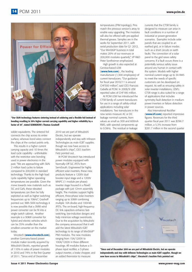
News from the exhibitionSpeaking about recovering from thecrisis in 2009, according to localsources Nuremberg-basedSEMIKRON (www.semikron.com)faced a loss of 30% down to €325
million in 2009. “But we grew byalmost 70% in 2010”, Head ofProduct Management ThomasGrashoff underlined. The privately-held company is one of the majorpower module suppliers and as sucha indicator of how the marketdevelops. Wind and solar power aswell as automotive were and are themajor growth drivers for SEMIKRONas well for the European powerelectronics industry in general. At PCIM Semikron introduced a
space-saving packaging technologywhich removes bond wires, soldersand thermal paste. The new SKiNTechnology is based on a flexible foiland sintered connections, doublingthe current density to 3 A/cm2
compared with 1.5 A/cm2 achievablewith standard wire bond technology.“The converter volume can thereforebe reduced by 35%. This reliableand space-saving technology is theoptimum solution for vehicle andwind power applications”, Grashoffcommented. Wire bonding has been the main
method of connecting the chipupper to a DBC substrate for thepast 25 years. Wire bonding is notup to the higher current density thattechnical advances have broughtabout, meaning reliability is impairedby bond lifting. With the new so-called SkiN packaging, a sintered foilreplaces the wire bonds on thechips, and the underside of the chipis sintered to the DBC. This results inbetter thermal and electrical chipconnection, since sintered layershave a lower thermal resistance than
PEE’s Special Session participants Regine Mallwitz/SMA (left), Ertugrul Sönmez/MicroGaN, Michael Briere/ACOO-IR, Robert Callanan/Cree, Mike Mazzola/SemiSouth, and Gerald Deboy/Infineon Technologies (right)
PCIM_Layout 1 15/06/2011 09:16 Page 12

ar europe
National Technology Park, Ashling Building, Limerick, Ireland • 353-61-504300 • www.ar-europe.ieIn UK, contact AR UK, www.uk-ar.co.uk or call +441-908-282766
Copyright © 2011 AR. The orange stripe on AR products is Reg. U.S. Pat. & TM. Off.
Our Support Is As StrongAs Our Products
Precision equipment demands precision care. That’s why it’s so important to have a companylike AR providing critical support.
AR’s trained engineers are available to perform installations, verification and calibration services,tech support, repairs, maintenance, upgrades, and more.
We provide quality services throughout Europe from our service centers in the UK, France, and Benelux,and as important as our first class support is the speed of our service.
Call us. We’ll help keep your equipment running like new.Contact: ar-europe.ie/contact/php
Visit http://goo.gl/379ZT to find out more.
13_PEE_0411_13_PEE_0411 15/06/2011 11:32 Page 1
14 PCIM 2011 www.pcim.de
Issue 4 2011 Power Electronics Europe www.power-mag.com
solder equivalents. The sintered foilconnects the chip across its entiresurface, whereas bond wires connectthe chips at the contact points only. This results in a higher current
carrying capacity and 10 times theload cycle capability - unthinkablewith the restrictive wire bondingused in power electronics in thepast. “We are approaching with SkiN2 million load cycles to failurecompared to 200,000 in standardtechnology. Thanks to the high loadcycle capability higher operatingtemperatures are possible. Given themove towards new materials such asSiC and GaN, these elevatedtemperatures can then be fullyexploited as well as higher switchingfrequencies up to 70kHz”, Grashoffpointed out. With SKiN technology itis now possible that a 3MW windpower converter can be fit into asingle switch cabinet. Anotherexample is a 90kW converter forhybrid and electric vehicles whichcan be 35% smaller than thesmallest converter on the markettoday. Vincotech (www.vincotech.com),
another Germany-based powermodule maker recently acquired byMitsubishi Electric, reported growthof 110% in sales of power modulesin 2010 and 74% in the first Quarterof 2011. “Since end of December
2010 we are part of MitsubishiElectric, but we operateindependently and stay with InfineonTechnologies as main IGBT supplier,though we now have access toMitsubishi’s chips”, CEO JoachimFietz pointed out. At PCIM Vincotech has introduced
power modules equipped withNormally-Off SiC JFETs fromSemiSouth. Engineered for highlyefficient solar inverters, these newproducts feature a 1200V dualbooster input stage and a 1200VMNPC (1 module per phase)inverter stage housed in a flow0package with just 12mm assemblyheight. The modules support highlyefficient, three-phase solar invertersranging up to 30kW combiningmultiple 10A diodes and 100m�
JFETs. The on-board, high-frequencyDC link capacitors enhance fast-switching, low-inductive designs andhelp minimize voltage overshoots.Due to the acquisition by Mitsubishithe company announced that it willadd the latest Mitsubishi IGBTtechnology to its range of MiniSKiiP®
PIM modules. The new modulesranging from 15A/1200V to100A/1200V in three differenthousings. All modules feature a 3-phase input rectifier, a 3-phaseoutput inverter, a brake chopper, andan added thermistor to measure
temperatures (PIM topology). Pinsmatch the previous version’s array toenable easy upgrading. The moduleswill also be offered with pre-appliedthermal grease. Samples are in theworks for September 2011, withserial production slate for Q1 2012.“Our MiniSKiiP business in totalmakes 20% of our revenues or200,000 modules quarterly”, VP R&DPeter Sontheimer emphasized.High growth is also expected at
Geneva-based LEM(www.lem.com) , the leadingmanufacturer (1,300 employees) ofcurrent transducers. “Our guidancefor fiscal year 2010/11 is aroundCHF300 million”, said CEO FrancoisGabella at PCIM. In 2008/9 LEMreported sales of CHF186 million. At PCIM LEM has introduced the
CTSR family of current transducersfor use in a range of safety-criticalapplications including solarinstallations. Two transducers in thenew series measure AC or DCleakage nominal currents, fromvalues as small as 300 and 600mARMS, with spectral components upto 9.5kHz. The residual or leakage
currents that the CTSR family isdesigned to measure can arise infault conditions in a number ofindustrial or power-generationscenarios. Examples include solarpanels that are coupled to anearthed grid, or in failure modessuch as a short circuits or earthfaults. The connection of a solarpanel to the grid raises safetyconcerns; if a fault occurs there is apotentially serious safety issuearound any human in contact withthe system. Models with highernominal current range up to 3A RMSto meet the needs of specificcustomers can be developed onrequest. As well as ensuring safety insolar inverter installations, LEM’sCTSR range is also suited for a rangeof applications that includessymmetry fault detection in mediumpower inverters or failure detectionin power sources.Also International Rectifier
(www.irf.com) reported impressivefigures. Revenues for the thirdquarter fiscal year 2011 was $296.7million, a 5.3% increase from$281.7 million in the second quarter
“Our SkiN technology features sintering instead of soldering and a flexible foil instead ofbonding resulting in 30% higher current carrying capability and higher reliability by afactor of 10”, stated SEMIKRON’s Thomas Grashoff
“Since end of December 2010 we are part of Mitsubishi Electric, but we operateindependently and stay with Infineon Technologies as main IGBT supplier, though wenow have access to Mitsubishi’s chips”, Vincotech’s Joachim Fietz pointed out
PCIM_Layout 1 15/06/2011 09:12 Page 14

www.power-mag.com Issue 4 2011 Power Electronics Europe
www.pcim.de PCIM 2011 15
fiscal year 2011 and a 22.7%increase from $241.9 million in thethird quarter fiscal year 2010. “Forthe June quarter, we expectrevenues of $320 million”, CEO OlegKhaykin stated. At PCIM the company introduced
the AUIR3330S Intelligent PowerSwitch (IPS) with a proprietary activedi/dt control feature that reducesconducted EMI and switching lossesto simplify design in automotivemotor drive applications. The new40 V high-side device combinesbootstrap regulator, charge pumpand high-side driver into a singlepackage. The load can be driven upto 40kHz at 100% duty cycle.Additionally, the IPS featuresprogrammable over-current andover-temperature protection requiredby applications operating in harshautomotive environments such aspumps and fans, and current sensingfeedback, a diagnostic function, verylow current consumption in sleepmode and ESD protection. “Our newactive di/dt control drasticallyreduces conducted EMI on the inputsupply without increasing switchinglosses, enabling a reduction in thesize of the EMI filter and the heatsink for more efficient compactmotor systems”, said Marc Legrain,IR’s Executive Director AutomotiveProduct Business Unit.Fuji Electric Co., Ltd.
(www.fujielectric.com) and
Freescale Semiconductor(www.freescale.com) entered intoan alliance on IGBT technology andproducts for HEVs and EVs. Workingwith Fuji Electric, Freescale will addhigh-power IGBT products to itsexisting portfolio of solutions forelectronic powertrain applications,market those products to itsautomotive customers and defineand produce new products based oncustomer input. “We are pleased towork with Freescale on IGBTtechnology and draw on theirautomotive capability”, commentedKuniaki Yanagisawa, GeneralManager of Fuji Electric’s ElectronicDevices Business Headquarters.SemiSouth (www.semisouth.
com) launched the TO-247SDP60S120D 1200V, 60A SiCpower Schottky diode, featuring apositive temperature coefficient forease of paralleling and temperature-independent switching behavior.“The new Schottky diode alsoexhibits a zero reverse recoverycurrent and zero forward recoveryvoltage and can replace threeparalleled 20A parts reducing powerdissipation by over 12% as well assaving space and cost”, commentdDieter Liesabeths, Director of Sales.The company also launched new45m�, 1200 V, normally-on trenchSiC power JFETs. These devicestarget a range of application spaces,including solar inverters, SMPS,
induction heating, UPS, windapplications, and motor drives.Featuring a positive temperaturecoefficient, the SJDP120R045 JFETsalso offer fast switching with no ‘tail’current - even up to its high 175°Cmaximum operating temperature ina TO-247 package. The device is alsoavailable in bare die form(SJDC120R045) for modulepartners. Infineon Technologies
(www.infineon.com) haspurchased real estate andmanufacturing facilities from theinsolvency Qimonda for a total of€100.6 million. The deal coverscleanroom and manufacturingfacilities as well as 300mmmanufacturing equipment forpotential volume processing of thin300mm power semiconductorwafers. For this purpose a pilot line isset-up at the company’s site inVillach/Austria. Some of the newmachinery will be used forcompletion of the pilot line in Villach.About the start and the location of a300mm volume production thecompany will decide during thecurrent fiscal year.At PCIM the company announced
the expansion of its ReverseConducting (RC) 600V IGBT withtwo new switching power devicesthat achieve up to 96% efficiency intarget applications. The new devicesallow design of energy efficient,electric-motor driven consumerappliances that use smallercomponents and thus have a loweroverall cost compared to alternativesystems. Also the 1200V SiC diode portfolio
has been extended with 1200Vdiodes in the new TO-247HC (HighCreepage) package. This newpackage layout is fully compatiblewith the industry standard TO-247and can therefore easily be placed inalready existing designs, without extraefforts. The higher creepage distanceincreases the safety margin againstthe risk of short circuits, especiallyarcing, which might be triggered bythe presence of dust or dirt inside thesystem. This reduces the need ofadditional chemical (silicone gel orcream) or mechanical solutions(sheaths or foils) needed to avoidany pollution between the packageleads, with all the benefits of a leanand fast manufacturing process.In higher power ranges Infineon
has launched 4.5kV IHV modulescombining TrenchSTOPTM and
FieldSTOPTM technology andcomplement the modules in the3300V and 6500V ranges. While theFieldSTOP structure ensures asignificant reduction in switchinglosses, the TrenchSTOP cellminimizes on-state power lossesbecause of its low saturation voltage.This results in lower losses andreduced cooling requirements, whichultimately decreases the systemcosts. The advantages of theTrenchSTOP technology furthermoreinclude good ruggedness and shortcircuit behavior, increased reliabilityand low electromagnetic interference(EMI). Infineon will sampling the4.5kV IHV modules for IGBT3/EC3initially in the IHM-B housing with astorage temperature down to -55°Cand an operating temperature up to150°C by end 2011, and secondly inthe highly insulated 6.5kV housingby mid 2012. ABB (www.abb.com/semiconductors) presented anewly developed 3.3kV high-temperature module generationrated at 1500A, which combines thedynamic properties of the previousSPT+ version with the 150°Coperation capability. This high-temperature operation waspreviously not possible due to thehigh leakage currents generated inthe IGBTs and the diodes. In the newversion the leakage current for theIGBT by optimizing the buffer andanode design results in an overallreduction by at least 30%, whilekeeping the bipolar gain andtherefore also the important dynamicproperties similar. The mainimprovement step has been takenon the diode-side. “Although theradiation lifetime control has beenidentified being rather prone toleakage current, we were able toreduce the leakage current by atleast a factor of 2 by carefullyadjusting the irradiation conditions tothe newly developed buffered anodedoping profile. This anode-designseparates the radiation defectsgenerated by the local lifetimecontrol laterally from the spacecharge region formed duringblocking. The challenge has been tomaintain the high safe-operating areaof the previous diode generation andcombine it with the desired hightemperature operation. The diode isable to withstand a very high dI/dt ofmore then 7kA/µs and the peakpower is exceeding 5.6MW”,explained ABB’s speaker SvenMatthias.
IR’s Marc Legrain showing demo board featuring AUIR3330S Intelligent Power Switchwith a proprietary active di/dt control feature that reduces conducted EMI and switchinglosses to simplify design in automotive motor drive applications
PCIM_Layout 1 15/06/2011 09:12 Page 15

16 POWER CONVERTERS www.teslaco.com
Issue 4 2011 Power Electronics Europe www.power-mag.com
98% Efficient Single-StageAC/DC Converter TopologiesA new Hybrid Switching Method is introduced in this article which for the first time makes possible AC/DCpower conversion in a single power processing stage providing both Power Factor Correction and isolationat high switching frequency. This single-phase rectifier is extended to a three-phase rectifier, which for thefirst time enables direct conversion from three-phase input power to output DC power resultingsimultaneously in the highest efficiency and lowest size. Slobodan Ćuk, President TESLAco, Irvine, USA
The goal of developing AC/DCconverters with Isolation and Power FactorCorrection (PFC) feature in a single powerprocessing stage and without a mandatoryfull-bridge rectifier has for years eludedpower electronics researchers (see coverimage). Present AC/DC convertersoperated from a single-phase AC line arebased on conventional Pulse WidthModulation (PWM) switching and processthe power through at least three distinctpower processing stages: full-bridgerectifier followed by boost PFC converterand another cascaded isolated full-bridgeDC/DC converter stage, which togetheruse a total of 14 switches and threemagnetic components resulting incorresponding efficiency, size and costlimitations. The new Hybrid Switching Method
enables new Single-Stage AC/DC convertertopology, the True Bridgeless PFCConverter* consisting of just three switchesand a single magnetic component albeit ata much higher efficiency approaching98%, having a 0.999 power factor and1.7% total harmonic distortion. Three-Phase Rectifier* consisting of three suchSingle-Phase Rectifiers* (*US and foreign
patents pending) takes for the first time afull advantage of Tesla’s three-phasetransmission system to convert constantinstantaneous input power of a three-phase system directly to a constant DCoutput power, albeit isolated at highswitching frequency, with near unity powerfactor (0.999), low total harmonicdistortion (1.7%), smaller size and lowercost but at ultra high efficiency of 98% [6].Serbian-American inventor Nikola Tesla
in 1879 invented the three-phase)transmission system, which together ACthree-phase motors and AC generatorsenabled a very efficient worldwide electricpower transmission and utilization, which isstill unsurpassed today. One of the keyproperties of Tesla’s three-phase system isthat it consists of three AC voltages eachdisplaced from the other by 120 degrees.When each phase is delivering the currentin phase and proportional to its respectiveAC line voltage (unity power factoroperation on each phase), theinstantaneous power from each phase ispositive (active) and is time varying.Nevertheless, the sum of the powers of allthree phases is constant in time (seeFigure 1). As this property is available on
both three-phase AC generator side andthree-phase AC load side there is noelectrical energy storage needed in such athree-phase long distance transmissionsystem. Yet, availability of the AC voltageson each side, make possible use of thethree phase AC transformers for steppingup the AC voltage on generator side andstepping-down AC voltage on the usersload side.
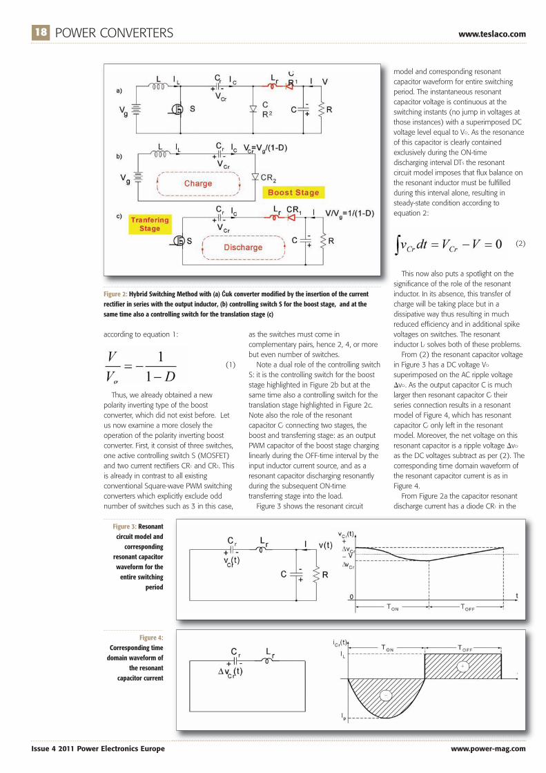
New boost converter topologiesThe new Hybrid Switching Method canbest be explained by way of an example.Shown in Figure 2a is the Ćuk converter[1,2] modified by the insertion of thecurrent rectifier CR1 in series with theoutput inductor which is now designatedas Lr where index r signifies a qualitativelychanged role of that inductor: from a PWMinductor in Square-Wave switching Ćukconverter to the resonant inductor. Theelimination of the PWM inductor alsoeliminates the inherent step-downconversion characteristic of the Ćukconverter and leaves only its step-up DCvoltage gain, albeit with the polarityinversion of the Ćuk converter remainingintact. Thus, the new DC voltage gain is
Figure 1: In Tesla’sthree-phase systemthe sum of the powerof all three phases isconstant in time
Teslaco_Feature_Layout 1 15/06/2011 09:24 Page 16

A superior performance from start to finish.�"(.������� �,����+���������������.&�'��% ���#�%�"% �!�����+#�����+�����&�)���"�'��� �'�%���&�����'����!�&&��'��%��+����%��&�!��'��% ��#�%�"% �!�����'��!"�����&�)��'"��"����'�����������������������('&
'��% ���� #���!���'"���- ��!���'��!��##����'�"!�#%�&&(%��"���(&'��� #&���'���!��)�!������&��+�%�#"&�'�"!��*�'�"('����� �!�'�!����"&�!������&�"!&'%�!�'��"%�&��%�����!��'��% ��#�%�"% �!���
Clean, consistent handlingfor precise auto-dispensing.��%�$(�&'.&�!�*�����������������&"�'�'���������#�%�"% �!���'��% ����!'�%����� �'�%�����&��&��!���&#���������+��"%�(&���!������)"�( ��('"���&#�!&�!���('"�#���� �!'��##����'�"!&���������������.&��!��%�!'�!�'(%���'������#&�'��� �'�%����"!�'�����%%��%���!�%�(%�!���"!)�%'�!���+�'��"!&�&'�!'�+��!�
����!�+�%����&�&��(%�!����&#�!&�!�����&�'�������%��'�%�&'������#&�'�� �'�%����&��(%��+�"!�'���'�%��'�&(%�����*�'��!"�!�����"%�����'�"!������&�)����+�%&�
��� +31 (0) 35 5380684 "% )�&�'�www.bergquistcompany.com/throughput
0 50 100 150 200
0.6
0.5
0.4
0.3
0.2
0.1Ther
mal
Impe
danc
e (ë
C-in2 /W)
Application Pressure (psi)
THERMAL PERFORMANCE
Sil-Pad 1500STTypical Thermal ImpedanceIncrease - Adhesive Layer
Sil-Pad®1500ST DeliversTrouble-free, HighThroughput DispensingWith Unequaled Thermal Performance.
Thermal Materials • Thermal Substrates • Fans and Blowers
�# �����������#� "� !� ��������"�� ����!�������������������� �� � ����������� ����� ���������� �����
17_PEE_0411_17_PEE_0411 15/06/2011 11:36 Page 1
18 POWER CONVERTERS www.teslaco.com
Issue 4 2011 Power Electronics Europe www.power-mag.com
according to equation 1:
(1)
Thus, we already obtained a newpolarity inverting type of the boostconverter, which did not exist before. Letus now examine a more closely theoperation of the polarity inverting boostconverter. First, it consist of three switches,one active controlling switch S (MOSFET)and two current rectifiers CR1 and CR2. Thisis already in contrast to all existingconventional Square-wave PWM switchingconverters which explicitly exclude oddnumber of switches such as 3 in this case,
as the switches must come incomplementary pairs, hence 2, 4, or morebut even number of switches.
Note a dual role of the controlling switchS: it is the controlling switch for the booststage highlighted in Figure 2b but at thesame time also a controlling switch for thetranslation stage highlighted in Figure 2c.Note also the role of the resonantcapacitor Cr connecting two stages, theboost and transferring stage: as an outputPWM capacitor of the boost stage charginglinearly during the OFF-time interval by theinput inductor current source, and as aresonant capacitor discharging resonantlyduring the subsequent ON-timetransferring stage into the load.
Figure 3 shows the resonant circuit
model and corresponding resonantcapacitor waveform for entire switchingperiod. The instantaneous resonantcapacitor voltage is continuous at theswitching instants (no jump in voltages atthose instances) with a superimposed DCvoltage level equal to VCr. As the resonanceof this capacitor is clearly containedexclusively during the ON-time discharging interval DTS the resonant circuit model imposes that flux balance onthe resonant inductor must be fulfilledduring this interval alone, resulting insteady-state condition according toequation 2:
(2)
This now also puts a spotlight on thesignificance of the role of the resonantinductor. In its absence, this transfer ofcharge will be taking place but in adissipative way thus resulting in muchreduced efficiency and in additional spikevoltages on switches. The resonantinductor Lr solves both of these problems.
From (2) the resonant capacitor voltagein Figure 3 has a DC voltage VCr
superimposed on the AC ripple voltage�vCr. As the output capacitor C is muchlarger then resonant capacitor Cr theirseries connection results in a resonantmodel of Figure 4, which has resonantcapacitor Cr only left in the resonantmodel. Moreover, the net voltage on thisresonant capacitor is a ripple voltage �vCr
as the DC voltages subtract as per (2). Thecorresponding time domain waveform ofthe resonant capacitor current is as inFigure 4.
From Figure 2a the capacitor resonantdischarge current has a diode CR1 in the
Figure 2: Hybrid Switching Method with (a) Ćuk converter modified by the insertion of the currentrectifier in series with the output inductor, (b) controlling switch S for the boost stage, and at thesame time also a controlling switch for the translation stage (c)
Figure 3: Resonantcircuit model and
correspondingresonant capacitorwaveform for theentire switching
period
Figure 4:Corresponding timedomain waveform of
the resonantcapacitor current
Teslaco_Feature_Layout 1 15/06/2011 09:24 Page 18

www.teslaco.com POWER CONVERTERS 19
www.power-mag.com Issue 4 2011 Power Electronics Europe
discharge loop. This diode permits only thepositive flow of current in the directiondictated by the diode. Moreover, the diodecannot turn-OFF until the resonantinductor current is reduced to zero at theend of ON-time interval, hence resonantcapacitor current is also zero as illustratedin the resonant capacitor current waveformin Figure 4. Since the resonant current isfull-wave sinusoidal waveform, theresonant capacitor current also must startat zero current level at the beginning of theON-time interval as illustrated in Figure 4as well.
From the resonant AC circuit model inFigure 5 the solutions for resonant currentand voltage are according to equations3/4:
(3)
(4)
A companion polarity non-invertingboost converter can be easily obtained bysimply inverting the polarity of the twooutput current rectifiers in Figure 2a andrelocating Lr to result in the converter ofFigure 5a. Note that current rectifiers arealso changing designation since CR2
rectifier is now conducting during OFF-timeinterval just as in conventional boostconverter. The flux balance on resonantinductor and PWM inductor as shown inFigure 5b results according to equations5/6 in:
(5)
(6)
Yet another converter topology is shownin Figure 6a in which the input voltagesource has a negative polarity resulting inpositive polarity of the output DC voltageand corresponding AC flux balance shownin shaded areas in Figure 6b. Note that thisconverter topology is analogous to theoriginal polarity inverting boost topology ofFigure 2a but with the source voltagebeing negative. Therefore the same resultsas previously derived are obtained forsteady-state DC voltages. Note the changeof the placement of the resonant inductorto the branch with the rectifier CR2. As the
resonant capacitor ripple voltage �vr is anorder of magnitude smaller than DCvoltage Vr, the flux of the resonant inductoris some 50 times smaller than that ofPWM inductor as seen by comparingshaded areas of the PWM inductor andresonant inductor. Clearly this results inresonant inductor physical size and losses
being negligible compared to PWM inputinductor.
True bridgeless PFC convertertopology Comparison of the converter topologies inFigures 2a/6a reveals that the polaritychange of the input source voltage results
Figure 5: Companion polarity non-invertingboost converter with (a) relocated resonanceinductor and (b) flux balance on resonant and
PWM inductor
Figure 6: Inverting boost topology of Figure 3abut with the source voltage being negative (a)and AC flux balance shown in shaded areas (b)
Teslaco_Feature_Layout 1 15/06/2011 09:24 Page 19

20 POWER CONVERTERS www.teslaco.com
Issue 4 2011 Power Electronics Europe www.power-mag.com
in positive and equal output DC voltagesgiven by (1) and (6), respectively.However, only one obstacle remains tomake these two topologies invariantrelative to the polarity change of the inputvoltage source and that is switching of theresonant inductor Lr placement from onediode branch to another. This problem canbe solved by placing resonant inductor forboth cases in branch with the resonantcapacitor Cr as illustrated in the converterof Figure 7. This now results intopologically invariant converter of Figure 7,which does not change its structureirrespective of the polarity of the sourcevoltage. Therefore, the source voltage canbe an AC voltage vAC which changes itspolarity as shown in Figure 7.
Note how the polarity of the inputsource automatically dictates which of thetwo rectifiers should be conducting duringwhich interval. Stated alternatively, the full-bridge rectifier on the front end is notneeded any more since the new convertertopology operates as the first true AC/DCconverter with the same DC voltage gainfor either polarity of input voltage. As theresult we obtained an AC/DC single-stageTrue Bridgeless PFC converter which canoperate directly from the AC line andwithout front-end bridge rectifier commonto conventional PFC boost converters. Asthe controlling switch S must change itscurrent direction and voltage blockingcapability depending on the polarity of theAC line voltage, it is implemented by aseries back-to-back connection of twoMOSFET switches.
In conventional boost converters thereare no good ways to introduce the isolation.The most popular is the Full-Bridge IsolatedBoost converter, which consists of fouractive controlling MOSFET switches on theprimary side and four-diode bridge on thesecondary side. The isolation transformer inthe True Bridgeless PFC converter, however,is introduced in Figure 8 which preservesthe original three-switch configuration andother advantageous of the original non-isolated configurations, such as low voltagestresses on all switches.
By controlling the input AC line current(at 50/60Hz) so that it is in phase and
Figure 7:Topologically
invariant converterwhich does not
change its structureirrespective of the
polarity of the sourcevoltage
Figure 8: True Bridgeless PFC Converter with isolation
proportional to input AC line voltage(Figure 8), the unity power factor and lowtotal harmonic distortion can be obtained.Note also that the PFC IC controller mustalso be a True Bridgeless PFC controller, asit needs to accept as its inputs the full-wave AC line voltage and full-wave AC linecurrents. Current PFC IC controllers, onthe other hand have as input rectified ACline voltage and rectified AC line current.These conventional PFC IC controllerscould still be used but with additionalsignal processing circuitry converting full-wave AC voltage and full-wave AC linecurrent into half-rectified ac waveform foruse with standard PFC IC controller.
The isolation transformer is of the bestkind (single-ended transformer of the Ćukconverter type) having magnetic core withthe BH loop as illustrated in Figure 9 with
Figure 9: Isolation transformer having magneticcore with bi-directional flux capability and
square-loop characteristic
bi-directional flux capability and square-loop characteristic, as there is no DC-biasin the transformer operation. Therefore,the design could be scaled up to high
Teslaco_Feature_Layout 1 15/06/2011 09:29 Page 20

SKiN TechnologyWire bond-free
Reliable and space-saving packaging technology for power semiconductors
Standard Technology
10 x higher power cycling
Free from thermal paste and solder
10 x higher power cycling
Free from thermal paste and solder
For 35% smaller inver
3 A/doubled: isnedtnerruC
10 x higher power cycling
tersFor 35% smaller inver
2cm3 A/t inurewopfoyt
10 x higher power cycling
21_PEE_0411_21_PEE_0411 15/06/2011 11:43 Page 1
22 POWER CONVERTERS www.teslaco.com
Issue 4 2011 Power Electronics Europe www.power-mag.com
power without the degradation of theperformance or the large size of magneticcore. In fact, the isolation transformer hasAC flux, which is at least four times lowerthan the flux in, for example, forwardconverter and bridge-type isolatedconverters. This directly translates inproportionally reduced size of themagnetics and increased efficiency.
Further improvements are obtained byintegration of the input inductor onto acommon core with the isolationtransformer [1,2,3, 5]. The placement ofthe air-gap on the magnetic leg withisolation transformer winding results inshifting of the input inductor high switchingfrequency ripple to the isolationtransformer resulting in ripple-free inputcurrent as seen in Figure 8 in addition toreduction of magnetics size to onemagnetic core only and further efficiencyimprovements.
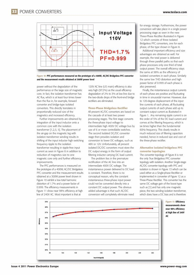
The PFC performances is measured onthe prototype of a 400W, AC/DC BridgelessPFC converter and the measurement resultsobtained at a 300W power level shown inFigure 10 exhibit a low total harmonicdistortion of 1.7% and a power factor of0.999. The efficiency measurements inFigure 11 show near 98% efficiency at highline of 240V AC. Most important is that at
120V AC line (US main) efficiency is alsovery high (97.2%) as the usual efficiencydegradation of 2% to 3% at low line due tothe two-diode drops of the front-end bridgerectifiers are eliminated.
Three-Phase Bridgeless RectifierAll present AC/DC converters are based onthe cascade of at least two powerprocessing stages. The first stage convertsthe three-phase input voltage tointermediate high 400V DC voltage bus byuse of 6 or more controllable switches.The second Isolated DC/DC converterstage then provides isolation andconversion to lower DC voltages, such as48V or 12V. Unfortunately, all presentisolated DC/DC converters must store theDC output energy in the form of outputfiltering inductor carrying DC load current.
The problem lies in the prematurerectification of the AC line into anintermediate 400V DC voltage. Theinstantaneous power delivered to DC loadis constant. Therefore, there is noconceptual reason, why the constantinstantaneous three-phase input powercould not be converted directly into aconstant DC output power. The obviousadded advantage is that such AC/DCconversion will completely eliminate need
for energy storage. Furthermore, the powerconversion will take place in a single powerprocessing stage as seen in the newThree-Phase Rectifier illustrated in Figure12 which consists of three IsolatedBridgeless PFC converters, one for eachphase, of the type shown in Figure 8.
Additional important efficiency and sizeadvantages are obtained as well. Forexample, the total power is deliveredthrough three parallel paths so that eachphase processes only one third of totaloutput power. The overall efficiency staysthe same at 98% as the efficiency ofisolated converters in each phase. Similarlythe same low THD distortion and highpower factor of 0.999 of each phase isalso preserved.
Finally, the instantaneous output currentsof each phase are positive and fluctuatingin time in sinusoidal manner. However, dueto 120-degree displacement of the inputline currents of each phase, all fluctuatingoutput currents of each phase add up toconstant output current as illustrated inFigure 1. Any remaining ripple current is onthe order of 5% of the DC load current andcomes at the filtering frequency, which issix times higher than the fundamental60Hz frequency. This clearly results inmuch reduced size of filtering capacitorsneeded, hence in reduced size and cost ofthe three-phase rectifier.
Alternative isolated bridgeless PFCconverter topologies The converter topology of Figure 8 is notthe only True Bridgeless PFC convertertopology with isolation. Another Single-stageAC/DC converter topology with PFC andisolation is shown in Figure 13 which can beused either as a Single-phase Rectifier orimplemented in converter of Figure 12 as aThree-Phase Rectifier. This converter has thesame DC voltage gain of the boost typesuch as [1] and has only one magneticpiece, the two winding isolation transformer,which does have a DC bias and is therefore
Figure 10: PFC performances measured on the prototype of a 400W, AC/DC Bridgeless PFC converterand the measurement results obtained at 300W power level
Figure 11: Efficiencymeasurements shownear 98% efficiencyat high line of 240VAC
Teslaco_Feature_Layout 1 15/06/2011 09:25 Page 22

www.teslaco.com POWER CONVERTERS 23
www.power-mag.com Issue 4 2011 Power Electronics Europe
suitable for low to medium power. Inaddition, the input current is pulsatingrequiring the use of the separate highfrequency filter on input to reduce ripplecurrents at high switching frequency.
The applications above have highlightedthe use of the new boost converter
topologies, the inverting and non-invertingones, for a single-stage True BridgelessAC/DC power conversion and theirapplication for single- and three-phaserectifiers which include galvanic isolation athigh switching frequency. However, thenew boost converter topologies have alsosignificant advantages when applied to
isolated DC/DC conversion. Shown in Figure 14 is the new isolated
boost DC/DC converter [4] used forconverting solar cell input power into ahigh voltage 400V DC bus. It canaccommodate the wide range of the inputvoltage of 15V to 100V (created by thevariation of solar cells voltages during theday) and generate regulated high DCvoltage isolated output of 400V withefficiencies of over 97%.
In current automotive applications forhybrid and electric vehicles, the auxiliary1kW to 2kW converters are needed toconvert the 400V battery voltage of thehigh voltage DC bus to 14V auxiliarybattery voltage and vice versa. Therefore abi-directional buck-boost converter isneeded. The converter of Figure 14implemented with MOSFET switchesinstead of current rectifiers on the output iscapable of such bi-directional power flowin a single power processing stage and iswell suited for these applications. Onceagain, the use of three switches onlyinstead of eight switches of conventionalconverters results in increased efficienciesand reduced cost at the same time.
Literature[1] Slobodan Ćuk, “Modeling,
Analysis and Design of SwitchingConverters”, PhD thesis, November1976, California Institute of Technology,Pasadena, California, USA.[2] Slobodan �uk, R.D. Middlebrook,
“Advances in Switched-Mode PowerConversion, “ Vol. 1, II, and III, TESLAco1981 and 1983.[3] Slobodan Ćuk, articles in Power
Electronics Technology, describingSingle-Stage, Bridgeless, Isolated PFCConverters published in July, August,October and November 2010 issues. [4] Slobodan Ćuk and Zhe Zhang,
Voltage Step-up Switching DC-DCConverter, US patent No. 7,778,046,August 17, 2010.[5] 99% Efficient AC/DC Converter
Topologies, Power Electronics Europe3/2011[6] Slobodan Ćuk, “Single-Stage,
AC-DC Converter Topologies of 98%Efficient Single Phase and Three-PhaseRectifiers”, Keynote at PCIM Europe2011, May 17, Nuremberg, Germany
Figure 12: Three-Phase Rectifier consisting of three Isolated Bridgeless PFC converters, one for eachphase, of the type shown in Figure 9
Figure 14: Isolated Boost DC/DC converter for converting solar cell input power into a high voltage400V DC bus
Figure 13: True Bridgeless isolated PFC Converter featuring two winding isolation transformer
To receive your own copy of
subscribe today at:
www.power-mag.com
Teslaco_Feature_Layout 1 15/06/2011 09:31 Page 23

2SP0115T Gate Driver Unleash the full power of your converter design using the new 2SP0115T Plug-and-Play driver. With its direct paralleling capability, the scalability of your design into highest power ratings is unlimited. Rugged SCALE-2 technology enables the complete
the size of 17mm dual modules. Combined with the CONCEPT advanced active clam-ping function, the electrical performance of the IGBT can be fully exploited while keeping the SOA of the IGBT. Needless to say that the high integration level provides the best possible reliability by a minimzed number of components.
FeaturesPlug-and-Play solution1W output power15A gate current<100ns delay time± 4ns jitterAdvanced active clampingDirect- and halfbridge modeDirect paralleling capability2-level and multilevel topologiesDIC-20 electrical interfaceSafe isolation to EN50178 UL compliant50.- USD @ 1000 pieces
www.IGBT-Driver.com
SAMPLES AVAILABLE!
CT-Concept Technologie AG, Renferstrasse 15, CH-2504 Biel, Switzerland, Phone +41-32-344 47 47
Unleash Sheer Power!
24_PEE_0411_24_PEE_0411 15/06/2011 11:38 Page 1
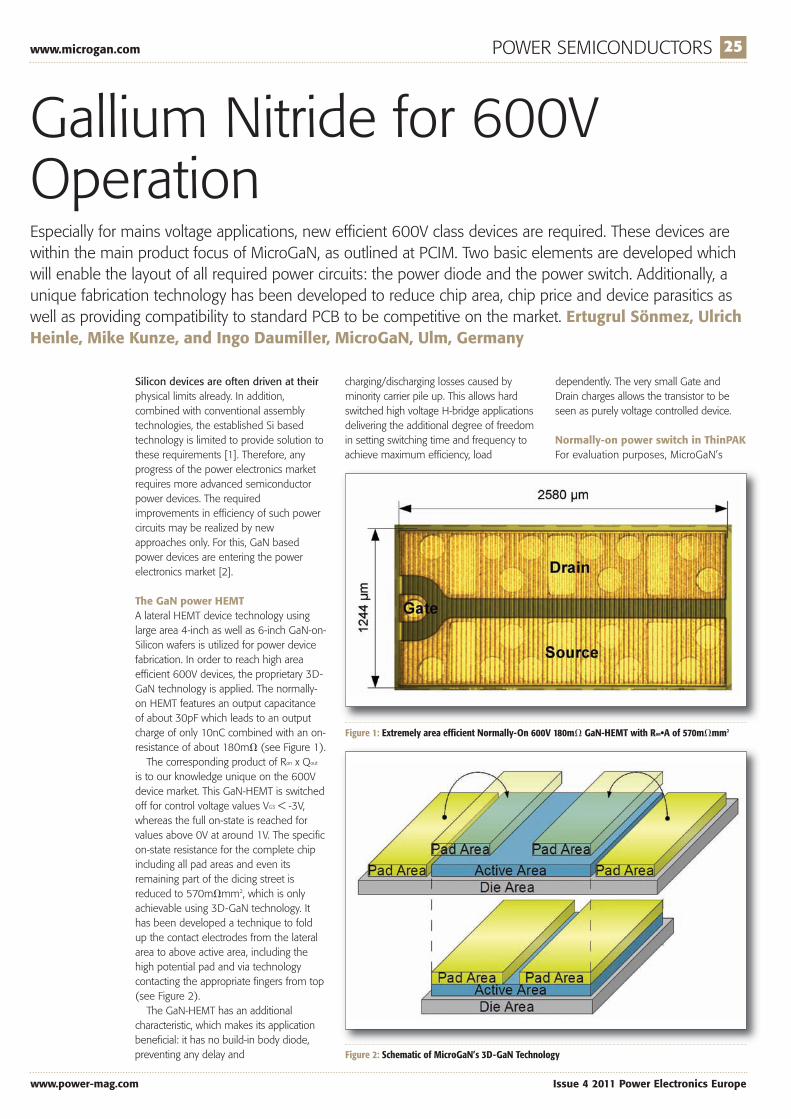
www.microgan.com POWER SEMICONDUCTORS 25
www.power-mag.com Issue 4 2011 Power Electronics Europe
Gallium Nitride for 600VOperationEspecially for mains voltage applications, new efficient 600V class devices are required. These devices arewithin the main product focus of MicroGaN, as outlined at PCIM. Two basic elements are developed whichwill enable the layout of all required power circuits: the power diode and the power switch. Additionally, aunique fabrication technology has been developed to reduce chip area, chip price and device parasitics aswell as providing compatibility to standard PCB to be competitive on the market. Ertugrul Sönmez, UlrichHeinle, Mike Kunze, and Ingo Daumiller, MicroGaN, Ulm, Germany
Silicon devices are often driven at theirphysical limits already. In addition,combined with conventional assemblytechnologies, the established Si basedtechnology is limited to provide solution tothese requirements [1]. Therefore, anyprogress of the power electronics marketrequires more advanced semiconductorpower devices. The requiredimprovements in efficiency of such powercircuits may be realized by newapproaches only. For this, GaN basedpower devices are entering the powerelectronics market [2].
The GaN power HEMTA lateral HEMT device technology usinglarge area 4-inch as well as 6-inch GaN-on-Silicon wafers is utilized for power devicefabrication. In order to reach high areaefficient 600V devices, the proprietary 3D-GaN technology is applied. The normally-on HEMT features an output capacitanceof about 30pF which leads to an outputcharge of only 10nC combined with an on-resistance of about 180m� (see Figure 1).The corresponding product of Ron x Qout
is to our knowledge unique on the 600Vdevice market. This GaN-HEMT is switchedoff for control voltage values VGS < -3V,whereas the full on-state is reached forvalues above 0V at around 1V. The specificon-state resistance for the complete chipincluding all pad areas and even itsremaining part of the dicing street isreduced to 570m�mm2, which is onlyachievable using 3D-GaN technology. Ithas been developed a technique to foldup the contact electrodes from the lateralarea to above active area, including thehigh potential pad and via technologycontacting the appropriate fingers from top(see Figure 2).The GaN-HEMT has an additional
characteristic, which makes its applicationbeneficial: it has no build-in body diode,preventing any delay and
charging/discharging losses caused byminority carrier pile up. This allows hardswitched high voltage H-bridge applicationsdelivering the additional degree of freedomin setting switching time and frequency toachieve maximum efficiency, load
dependently. The very small Gate andDrain charges allows the transistor to beseen as purely voltage controlled device.
Normally-on power switch in ThinPAKFor evaluation purposes, MicroGaN’s
Figure 1: Extremely area efficient Normally-On 600V 180m� GaN-HEMT with Ron•A of 570m�mm2
Figure 2: Schematic of MicroGaN’s 3D-GaN Technology
Microgan Feature_Layout 1 15/06/2011 09:40 Page 25
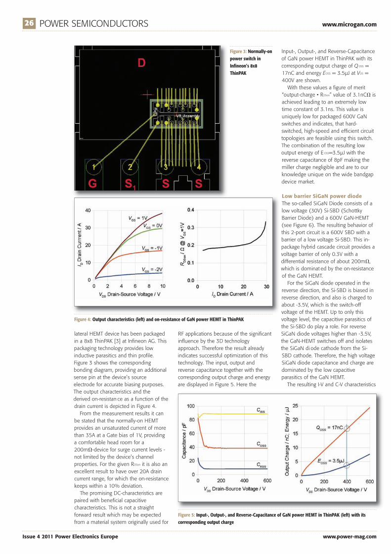
26 POWER SEMICONDUCTORS www.microgan.com
Issue 4 2011 Power Electronics Europe www.power-mag.com
lateral HEMT device has been packagedin a 8x8 ThinPAK [3] at Infineon AG. Thispackaging technology provides lowinductive parasitics and thin profile.Figure 3 shows the correspondingbonding diagram, providing an additionalsense pin at the device’s sourceelectrode for accurate biasing purposes.The output characteristics and thederived on-resistan ce as a function of thedrain current is depicted in Figure 4.From the measurement results it can
be stated that the normally-on HEMTprovides an unsaturated current of morethan 35A at a Gate bias of 1V, providinga comfortable head room for a 200m�-device for surge current levels -not limited by the device’s channelproperties. For the given RDSon it is also anexcellent result to have over 20A draincurrent range, for which the on-resistancekeeps within a 10% deviation.The promising DC-characteristics are
paired with beneficial capacitivecharacteristics. This is not a straightforward result which may be expectedfrom a material system originally used for
RF applications because of the significantinfluence by the 3D technologyapproach. Therefore the result alreadyindicates successful optimization of thistechnology. The input, output andreverse capacitance together with thecorresponding output charge and energyare displayed in Figure 5. Here the
Input-, Output-, and Reverse-Capacitanceof GaN power HEMT in ThinPAK with itscorresponding output charge of Q OSS =17nC and energy EOSS = 3.5µJ at VDS =400V are shown.With these values a figure of merit
“output-charge • RDSon” value of 3.1nC� isachieved leading to an extremely lowtime constant of 3.1ns. This value isuniquely low for packaged 600V GaNswitches and indicates, that hard-switched, high-speed and efficient circuittopologies are feasible using this switch.The combination of the resulting lowoutput energy of E OSS=3.5µJ with thereverse capacitance of 8pF making themiller charge negligible and are to ourknowledge unique on the wide bandgapdevice market.
Low barrier SiGaN power diodeThe so-called SiGaN Diode consists of alow voltage (30V) Si-SBD (SchottkyBarrier Diode) and a 600V GaN-HEMT(see Figure 6). The resulting behavior ofthis 2-port circuit is a 600V SBD with abarrier of a low voltage Si-SBD. This in-package hybrid cascade circuit provides avoltage barrier of only 0.3V with adifferential resistance of about 200m�,which is dominat ed by the on-resistanceof the GaN HEMT. For the SiGaN diode operated in the
reverse direction, the Si-SBD is biased inreverse direction, and also is charged toabout -3.5V, which is the switch-offvoltage of the HEMT. Up to only thisvoltage level, the capacitive parasitics ofthe Si-SBD do play a role. For reverseSiGaN diode voltages higher than -3.5V,the GaN-HEMT switches off and isolatesthe SiGaN di ode cathode from the Si-SBD cathode. Therefore, the high voltageSiGaN diode capacitance and charge aredominated by the low capacitiveparasitics of the GaN HEMT.The resulting I-V and C-V characteristics
Figure 3: Normally-onpower switch inInfineon’s 8x8ThinPAK
Figure 4: Output characteristics (left) and on-resistance of GaN power HEMT in ThinPAK
Figure 5: Input-, Output-, and Reverse-Capacitance of GaN power HEMT in ThinPAK (left) with itscorresponding output charge
Microgan Feature_Layout 1 15/06/2011 09:40 Page 26
www.microgan.com POWER SEMICONDUCTORS 27
www.power-mag.com Issue 4 2011 Power Electronics Europe
of the SiGaN diode are shown in Figure7, where the described characteristics ofthe SiGaN diode circuit elements can belocated individually. From the SiGaNdiodes forward characteristic, the typicallow barrier voltage can be extracted aswell as the differential resistance ofabout 200m�, resulting in 4A diodecurrent at 1.2V forward voltage. To ou rknowledge this behavior also is uniquefor a diode missing minority carrierstored charge with just 18.6nC overallcharge. With at least comparable chargevalues to SiC-SBD one obtains anunbeatable low onset voltage.
From the C-V-characteristics, the GaNHEMT switching off can be seen whichisolates the Si-SBD during themeasurement: within a few volt sweepthe capacitance of the SiGaN diodedrops from ove r 1700pF to about 60pFand reaches a value of just 43pF at -100V.
The application benefit of this cascadeis manifold. Used as a PFC-Diode, it willpass current starting already at 0.3V,which gives an excellent tool for wideefficiency bandwidth solutions. The lowSiGaN diode charge allows a highswitching speed from this device point ofview, providing the possibility to go forhigher power density design s. Used as afreewheeling diode, it catches the current at already 0.3V, preventing theon-set of the body diode current flow ofa Si-600V-HV device. Thus, charging ofseveral µC and a harming recovery time of several hundred ns areprevented.
A normally-off functionality can bederived from a normally-on core unitdevice by an in-package hybrid cascodecircuitry (see Figure 8). The cascodeconsists of a lo w voltage (30V) Si-MOSFET in common-source and a highvoltage GaN-HEMT in common-gateconfiguration. The resulting 3-port circuitagain acts as a switch. In its on-mode theparasitic on-state resistance of the Si-MOSFET (<20m�) and the one of theGaN-HEMT are added to about 320m�.The obvious increase above the expectedsum value is due to the internal biasingof the GaN HEMT which leads to on-state bias condition slightly below fullopen channel. In the off-state of thecascode the Si-MOSFET is switching offthe GaN-HEMT and is charged to about3.5V, analog to the SiGaN diode. Hereagain, the Drain of the GaN-HEMT isdefining the 600V behavior of thecascode.
Figure 9 displays the transfercharacteristics and the off-statecharacteristics of the cascode. Asexpected, the Si-MOSFET defines and
Figure 6: SiGaN Diode - cascade circuit of a low voltage Si-SBD with a high voltage GaN-HEMT
Figure 7: Power Diode forward characteristics showing its typical low on-set voltage of 0.3V (left) andits reverse C-V-Characteristics with the low capacitance of 43pF
Figure 8: Normally-off power switch by cascode circuit made of a low voltage Si-MOSFET and a highvoltage GaN-HEMT
Figure 9: Transfer-characteristics of the cascode using HV GaN-HEMT (left) and its off-statecharacteristics up to 600V for VGS=0V
Microgan Feature_Layout 1 15/06/2011 09:40 Page 27

28 POWER SEMICONDUCTORS www.microgan.com
Issue 4 2011 Power Electronics Europe www.power-mag.com
controls the drain current of the cascode,which results in an off-state for VGS=0V.The high voltage off-state characteristicsreveal the present leakage current levelof MicroGaN’s normally-on devices ofaround 900µA at 600V, here measuredat VGS=0V.In the reverse operation mode of the
cascode (VDS<0V), the GaN-HEMT is inthe on-state as a parasitic resistor(180m�) in series to the Si-MOSFET. Ifthe Si-MOSFET is in the off-state, its bodydiode provides a current path at itscharacteristic voltage.By using a cascode, one combines the
advantages of the LV Si-MOSFET (usuallya high quality body diode, low charge asoperated at 3.5V) and these of the GaN-HEMT (high speed, no body diode, low-est possible charge). On the other hand,one has to pay attent ion to the setupparasitics of the circuit in order toprevent ringing.The setups of the cascade and
cascode are designed carefully to preventthe commonly made error of inductivesetup technology ceasing the chip-devicefrom operation at high di/dt in thepackage.This cascode is predestinated to be
used in hard switched high switching
speed PFCs as well as in H-bridge,maintaining the high peak and wideban dwidth in efficiency.
ConclusionsThe market demand for high efficientnew approaches is discussed using theexample of a mains voltage down-conversion and its specific need of highefficient 600V power devices. The basiccircuit construction elements - the lowbarrier (0.3V) power diode and thenormally-off power switch - werepresented and discussed in detail [4] asthey are derived from a unique core un itdevice: the GaN power HEMT, which hasbeen packaged and tested in a 8x8ThinPAK by Infineon AG. Next steps willbe the transfer of the presentedcharacteristics into their dynamicequivalents and the setup of applicationdemonstration.As a result, surpassing circuit
efficiencies will be possible using thepresented elements.Furthermore, by combining the
cascode and cascade, one may obtain anunique pair o f design elements forrealization of efficient motor driveapplications, also.We would like to acknowledge the
fruitful cooperation with Infineon AG,within which MicroGaN’s devices havebeen tested in the framework of theGerman subsidiary project NeuLand,which is sponsored by the FederalMinistry of Education and Research(BMBF).
Literature[1] “Keynote: Is it the End of the
Road for Silicon in PowerConver sion?”, A. Lidow, Efficient PowerConversion Corporation, El Segundo,United States, CIPS 2010, 6th International Conference onIntegrated Power Electronics Systems,Nuremberg, Germany.[2] “Power GaN”, GaN technologies
for power electronics applications:Industry and market status &forecasts, YOLE Development.[3] 8x8 ThinPAK,
http://www.infineon.com/cms/en/product/promopages/IMM/ThinPAK/index.html[4] E. Sönmez, “Efficient GaN
Products for 600V Operation”, PEESpecial Session “High FrequencySwitching Devices and Applications”at PCIM 2011, Nuremberg, Germany.
Microgan Feature_Layout 1 15/06/2011 09:40 Page 28

www.infineon.com, www.sma.de SOLAR POWER 29
www.power-mag.com Issue 4 2011 Power Electronics Europe
New SiC JFET BoostPerformance of Solar InvertersThe article proposes a new normally-on Silicon Carbide (SiC) JFET device concept with monolithicallyintegrated body diode. The new device combines ultra fast switching with ohmic forward characteristic anda zero reverse recovery characteristic of its body diode. It allows a significant boost of the performance ofsolar inverters especially in the light of new requirements such as reactive power capability and fault ridethrough. Best device performance is achieved with a direct driven approach, compatible with safety aspectsin voltage driven topologies which is implemented in combination with a low voltage MOSFET. Gerald Deboy, Roland Rupp, Infineon Technologies Austria/Germany, and Regine Mallwitz,Holger Ludwig, SMA Solar Technology, Germany
SiC devices are characterized by anumber of promising properties like lowswitching losses, high rated voltages, highoperating temperature, high radiation
hardness, which were discussed earlier in[1,2]. In the laboratory the potential of SiCMOSFET and SiC JFETs [2-4] in solarinverters have been demonstratedconcerning improvements of efficiency andsize reduction. This article focuses oninvestigation of the new SiC JFET in analready existing photovoltaic (PV) inverterplatform. Challenges here are theassessment of the safety risk due tonormally-on characteristic combined withthe proof of an increased efficiency underthe restriction of EMI demands.
SiC device concept with integratedbody diodeWe believe that a JFET structure without achannel being formed below a gate oxideas shown in Figure 1 has strategicadvantages over a SiC MOSFET. First, thereliability aspect is easy to meet in a JFETstructure but difficult in a MOS structure
due to the still high density of extrinsicdefects in the oxide. Second, the stillunsatisfying subthreshold behavior ofMOSFETs at high temperature does not
Figure 1: Cross section of the proposed SiC JFETdevice concept
Figure 2: Comparison of hard commutation of the body diode of a 100m�/1200V SiC JFET (right) vsthe recovery perfomance of a 1200V/15A SiC Schottky barrier diode (left) at load current ID=30A,VDS=800V, Rg=3�; (Channel 2: Drain voltage, Channel 3: Gate voltage, Channel 4: Current; time base100ns/div)
exist in a JFET. This issue is important forthe leakage current and may hurt theefficiency of the entire converter. And lastbut not least the structural elements of aSiC JFET are very close to the structuralelements of SiC Schottky barrier diodes,which are selling in millions of pieces withproven quality in the field.
The proposed SiC JFET concept has abipolar diode integrated between the p-well contacted by source and the backsidedrain contact. This diode can handle thefull current rating of the SiC JFET. Beyondthe obvious advantages of driving the JFETin a synchronous rectification manner thebody diode is still needed for the deadtime between the switching intervals ofopposite devices, in an e.g. DC/AC output
Infineon Feature_Layout 1 15/06/2011 09:49 Page 29

30 SOLAR POWER www.infineon.com, www.sma.de
Issue 4 2011 Power Electronics Europe www.power-mag.com
bridge. If this diode is not present in thedevice structure a full current rated SiCSchottky barrier diode has to beimplemented additionally for parallelingwith the SiC JFET. During hardcommutation the body diode of theproposed SiC JFET shows practically zeroreverse recovery charge. This behavior isotherwise known only from SiC Schottkybarrier diodes.
Experimental JFET resultsFigure 2 compares the hard commutationof a 15A SiC Schottky barrier diode with a100m� SiC JFET. Both waveforms show avery similar characteristic with the reverse
recovery current flowing nearly only duringthe voltage rise. This is a strong indicatorfor a pure capacitive displacement currentin both devices.
Figure 3 shows the comparison of turn-on losses in a JFET half bridge
configuration versus a combination ofJFET as switch and a SiC Schottky diodeas freewheeling element. The switchingbehavior of the SiC JFET shows both veryfast turn on and turn off behavior. Incomparison to commercially available1200V trench-IGBTs based on field-stoptechnology a reduction of both turn-onand turn-off energy of one order ofmagnitude has been observed. Incomparison to IGBT technologies with aspecific high speed optimization theswitching losses are lower by a factor of2. These ultra low switching losses arethe natural key to move towards higherswitching frequencies needed for the costreduction of the magnetic components.Figure 4 shows the respectivecomparison.
Solar inverters and theirrequirements to powersemiconductorsFrom all types of PV inverters stringinverters [6] are manufactured in thehighest number of pieces. Due to thismarket relevance a string inverter waschosen as a platform for the followinginvestigations. String inverters arecharacterized by an output power rangefrom 1kW up to about 20kW, comprisingsingle phase or three phase topologiesand showing very high efficiencies up to98%. Typically power semiconductors withrated voltages between 600V and 1200Vare being used at RMS currents between10A and 50A. The switching frequency isin the range of 16kHz to 48kHz. TodaySilicon (Si) based IGBTs and MOSFETs arecommonly used in this application.However, Si diodes are already replacedstep by step with SiC Shottky diodes.
For increased efficiencies suitabletopologies in combination with low-losspower semiconductors are required. Overthe years a number of PV specifictopologies have been developed. They canbe analyzed for instance by the number ofphases (one, two or three phases),galvanic isolation (transformer less or withtransformer), the kind of transformer (LF orHF) or which DC potential can begrounded to earth [7]. Due to the
Figure 3: Comparison of turn-on losses of the new 1200V/100m� SiC JFET with a 1200V/15A SiCSchottky barrier diode versus the body diode of the SiC JFET as freewheeling diode at VDS=800V, Tj =75°C, Rg=3�
Figure 4: Comparison of switching losses (turn-on plus turn-off) of a 1200V-50m� SiC JFET vs acombination of a high-speed optimized IGBT with a SiC Schottky barrier diode and a conventional1200V IGBT combined with a fast Si pin-diode at VDS=800V, Tj =75°C, Rg =3�
Figure 5: Topologies for PV inverters: NPC (left)and BSNPC (right)
Infineon Feature_Layout 1 15/06/2011 09:49 Page 30
www.infineon.com, www.sma.de SOLAR POWER 31
www.power-mag.com Issue 4 2011 Power Electronics Europe
improved flexibility for the PV moduleconfiguration on roof tops, for which asignificant wider input voltage range isadvantageously, often an inverter topologyis combined with a boost or buck stagebetween PV generator and the inverter.Typical inverter topologies are the wellknown H-bridge, the PV specific H5 orHERIC bridges or multilevel arrangementslike the Neutral Point Clamped (NPC) orBipolar Switch Neutral Point Clamped(BSNPC) topology [8]. Figure 5 shows foreach one leg: a NPC (left) and a BSNPC(right) connected to a PV generatorfollowed by a divided DC link capacitor.Both topologies use four switches A1 to
A4. The high and low side switches A1 andA4 are switched at high frequency (e.g.16kHz), the switches A2 and A3 operate atgrid frequency. In the NPC one of thediodes D5 or D6 in combination with oneof the switches A2 or A3 clamps thevoltage to the half of the PV voltage if oneof the corresponding switches A1, A4 isturned off. Which pair of diode and switchis active, depends on the polarity of thegrid voltage. In every case the load currentflows through two switches connected inseries: A1, A2 or A3, A4. In the BSNPC a bipolar switch arranged
by A2, A3, D2 and D3 clamps the voltageto the half of the PV voltage if one of theprevious two switches is turned off. In thiscase, most of the load current flows onlythrough one switch A1 or A4. By using Sisemiconductors for all switches anefficiency of 98.2% in maximum for thewhole inverter system can be obtained.The use of SiC JFETs for A1 and A4enhances the inverter efficiency inparticular.
Construction and topology of PVinverter with new SiC JFETFor this research presentation existingthree-phase PV string inverter SUNNY
TRIPOWER with a maximum output powerof 17kW by SMA acts as a platform. Figure 6 shows an exploded drawing of
the inverter assembly. The heart of thedevice is an integrated housing made ofaluminum die cast. This housing has aninner separating wall which separates theinverter in a front and a backcompartment. On the front side acompartment for sensitive electroniccomponents like semiconductors is
situated. All modules are thermallycoupled to the separation wall of thehousing. Mounting places are marked. Onits backside cooling fins are located sothat the housing acts as the coolingsystem. Generally on the backside heatgenerating components such asembedded inductive component areassembled for cooling.The inverter uses a two-stage topology
consisting of two boosters for theconnection of two strings of PV modulesand a three-phase BSNPC topology. Allsemiconductors are integrated in fiveEasy1b modules from InfineonTechnologies: two booster modules andthree inverter modules. The two boostermodules include semiconductors for thebooster stages. Each of the invertermodules is configured as one leg of theBSNPC topology. The configuration ofsemiconductors and the semiconductormodule is represented in Figure 7. High and low side transistors A1, A4
(see Figure 5) are replaced by normally-onSiC JFETs. To prevent a short circuit duringstart up of the system a Cascode formedby a direct driven JFET and a serial lowvoltage MODFET was introduced [9]. Herea low voltage MOSFET is arranged in seriesto one JFET. Both switches are driven
Figure 6: Exploded view to a three phase PV inverter - Sunny TRIPOWER [6]
Figure 8: Three-phase BSNPC with direct driven SiC JFETs at high and low side positions in a Cascodeconfiguration
Figure 7: Semiconductor inverter module Easy1b and its PV specific equipment
Infineon Feature_Layout 1 15/06/2011 09:49 Page 31
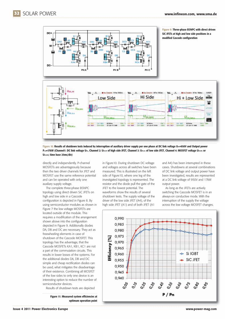
32 SOLAR POWER www.infineon.com, www.sma.de
Issue 4 2011 Power Electronics Europe www.power-mag.com
Figure 9: Three-phase BSNPC with direct drivenSiC JFETs at high and low side positions in amodified Cascode configuration
Figure 10: Results of shutdown tests induced by interruption of auxiliary driver supply per one phase at DC link voltage UDC=950V and Output powerPout=17kW (Channel1: DC link voltage UDC, Channel 2: UDS,JHi of high side JFET, Channel 3: UDS,JLo of low side JFET, Channel 4: MOSFET voltage UDS,Mlo or UDS,MHi; time base 25ms/div)
directly and independently. P-channelMOSFETs are advantageously becausethen the two driver channels for JFET andMOSFET use the same reference potentialand can be operated with only oneauxiliary supply voltage. The complete three-phase BSNPC
topology using direct driven SiC JFETs onhigh and low side in a Cascodeconfiguration is depicted in Figure 8. Byusing semiconductor modules as shown inFigure 7 the low voltage MOSFETs arelocated outside of the module. Thisrequires a modification of the arrangementshown above into the configurationdepicted in Figure 9. Additionally diodesDA, DB and DC are necessary. They act asfreewheeling elements in case ofshutdown of the Cascode MOSFET. Thistopology has the advantage, that theCascode MOSFETs KA1, KB1, KC1 are nota part of the commutation circuits. Thisresults in lower losses of the systems. Forthe additional diodes DA, DB and DCsimple and cheap rectification diodes canbe used, what mitigates the disadvantageof their existence. Combining all MOSFETof the low sides to only one device is aninteresting option to reduce the number ofsemiconductor devices.Results of shutdown tests are depicted
Figure 11: Measured system efficiencies atoptimum operation point
in Figure10. During shutdown DC voltageand voltages across all switches have beenmeasured. This is illustrated on the leftside of Figure10, where one leg of theinvestigated topology is represented. Theresistor and the diode pull the gate of theJFET to the lowest potential. Thewaveforms show the results of severalshutdown tests. The supply voltage of thedriver of the low side JFET (A4), of thehigh side JFET (A1) and of both JFET (A1
and A4) has been interrupted in thesecases. Shutdowns at several combinationsof DC link voltage and output power havebeen investigated, results are representedat a DC link voltage of 950V and 17kWoutput power. As long as the JFETs are actively
switching the Cascode MOSFET is in analways-on conductive mode. With theinterruption of the supply the voltageacross the low voltage MOSFET changes.
Infineon Feature_Layout 1 15/06/2011 09:49 Page 32

www.infineon.com, www.sma.de SOLAR POWER 33
www.power-mag.com Issue 4 2011 Power Electronics Europe
The MOSFET turns-off immediately, whichputs the entire Cascode formed by theJFET and the low voltage MOSFET into theoff-state. Later on after one and a halfperiod of the AC voltage the relay betweeninverter and grid opens and realizes thedisconnection from the grid. After openingthe relay the voltage over the JFETs risesslowly up to their stationary value. Withthese pictures the safe operation of thedirect driven Cascode in the application isdemonstrated.
Experimental inverter resultsFigure 11 shows efficiencies of the invertersystem at optimum operation point overseveral output power levels. A significantdifference between both solutions can beseen. The standard inverter based on Siswitches achieves a maximum efficiency of98.2%. For the inverter equipped with thenew SiC JFETs 98.8% system efficienciescan be obtained. EMI and efficiency tests have been
done for several current rise rates. Inprinciple a shorter switching time andhence a further increase of efficiency ispossible. But this is in contradiction withEMI demands. An improvement of theEMI behavior is expected with anoptimization of the PCB andsemiconductor module layout, which willallow further increase the efficiency.
ConclusionsThis article presents a new normally-onSiC JFET with monolithically integratedbody diode. The device concept achievesohmic characteristics in forward andreverse direction (when driven in a“synchronous rectification” mode) andextremely low switching losses. It showsa nearly zero reverse recoveryperformance of its monolithically bodydiode.
Safety requirements can be fulfilled bycombining the direct driven normally-on
SiC JFET with a low-voltage MOSFET in aCascode arrangement. This pair ofswitches operates like one normally-offswitch in critical situations. Topology andfunctionality tests have been presentedin this paper. The influence of theCascode MOSFETs on the systemefficiency is extremely low.SiC JFETs reduce static and dynamic
lo sses significantly in comparison to Si-based switches resulting in a clearimprovement of the PV inverterefficiency. Experimental resultsdemonstrating this have been presentedand discussed showing that efficienciesas high as of 98.8% could be reached.All required EMI tests have been passed.Further improvements are expected byan optimization of PCB and modulelayout. The new SiC JFETs are suitable fo ran improvement of efficiency or outputpower of PV inverters. Even an increasingof switching frequency can be expectedat the same level of losses compared tothe existing solution, based on Sitransistors. This leads to a reduced sizeof inductive components. Smallerinductive components can make asignificant contribution to cost reductionof PV systems.The new SiC JFET allows full usage of
the integrat ed body diode. It saves anti-parallel diodes in the topology, which areotherwise required in the case of reactivepower. Due to the relatively high on-statevoltage of the body diodes the turn-on ofthe channel in parallel to the diode in asynchronous rectification mode isstrongly recommended. The new SiCJFET is hence an ideal choice in bothforward and reverse operation, asoutlined at PCIM 2011 [10].
Literature[1] Burger D. Kranzer, F. Reiners,
C. Wilhelm, B. Burger: SystemImprovements of Photovoltaic In-
verters with SiC-Transistors.ICSCRM2009, Nuremberg, October2009.[2] Zacharias, P.: Perspectives of SiC
Power Devices in Highly EfficientRenewable Energy Conver-sionSystems. ECSCRM 2008.[3] Wilhelm, C.; Kranzer, D.; Burger,
B.: Development of Highly Compactand Efficient Solar Inverter with Silico nCarbide Transistors. CIPS 2010,Nuremberg, March 2010.[4] Sahan, B.; Araujo, S.; Kirstein, T.;
Menezes, L.; Zacharias, P.:“Photovoltaic converter topologiessuitable for SiC JFETs”, PCIM 2009,Nuremberg, May 2009.[5] Friedrichs, P. et al (editors),
Silicon Carbide, Vol. 2, Power Devicesand Sensors, Wiley VCH, ISBN 978-3-527-40997-6.[6] Mallwitz, R.; Engel, B.: Solar
Power Inverters. CIPS 2010,Nuremberg , March 2010.[7] Engel, B.; Mallwitz, R.; Victor, M.:
Leistungselektronik bei dezentralenerneuerbaren Energien - insbesonderebei Photovoltaik-Wechselrichtern.Bauelemente der Leistungselektronikund ihre Anwendungen. ETG-Fachtagung, Bad Nauheim, April2011.[8] Falk, A.; DeBrabandere, K.;
Greizer, F.; Victor, M.; Westphal, T.;Wolf, H.; Bülo, T.: EP2107672A1.[9] Domes, D.; Zhang, X.: CASCODE
LIGHT - norma lly-on JFET stand aloneperformance in a normally-offCascode circuit. PCIM 2010,Nuremberg, May 2010.[10] Mallwitz, R; Deboy, G: New SiC
JFET with Integrated Body DiodeBoosts Performance of PhotovoltaicSystems; PEE Special Session “HighFrequency Switching Devices andApplications” at PCIM 2011,Nuremberg, Germany
To receive your own copy of
Power Electronics Europe
subscribe today at:
www.power-mag.com
Infineon Feature_Layout 1 15/06/2011 09:49 Page 33

34 THERMAL MANAGEMENT www.kerafol.com
Issue 4 2011 Power Electronics Europe www.power-mag.com
Efficient LED HeatManagementLEDs are being used in more and more ways. Due to their brightness, high efficiency and long lifeexpectancy, they continue to conquer domains that only recently were reserved for traditional light sources.This means that driver electronics must be adapted to an ever-increasing number of applications. Markus Eißner, Ingenieurbüro Eissner for Kerafol, Eschenbach, Germany
This raises the question of how thecomponents’ lost heat enters the heat sink.For this, a good thermal transition must befound. Because SMD components areused in most applications, the heat mustbe brought to the heat sink through aprinted circuit board (PCB). This producestwo step heat transfers that make up thegreater part of the system’s overall heatresistance.
Heat transfer characteristicsAn LED can have an average lifetime ofabout 50,000 hours when TJ = 25°C.When TJ = 125°C, the average lifetimeshortens to 25,000 hours. When TJ =175°C, a lifetime of only 100 hours isspecified. This is why careful heatmanagement is very important for LEDs.The printed circuit board is a very bad
heat conductor, with heat conductivity (�)of about 0,3W/m·K when FR4 printedcircuit board material is used. The resultingtemperature increase through the PCBduring induced heat output is calculated as
�T = (Q * d) / (� * A) [K]
where d is the thickness of the PCB in [m],and Q is the heat output in [W].To increase the PCB’s heat conductivity,
vias are placed in a hexagonal pattern inthe PCB. The vias partially increase theheat conductivity. The costs incurred duringPCB production are minimal. If the createdheat is high, copper rivets are used. Forthis, the round notches in the PCB aremilled and the copper rivets are inserted.The SMD component is soldered onto therivet, which has good heat conductivity. The next important transfer is from the
PCB to the heat sink. For this there areseveral possibilities. One good solution isto lay a heat-conductive film between thePCB and the heat sink. This performsseveral tasks at the same time. The firsttask is to conduct heat away continuously.The second task is to even out theirregularities between the printed circuitboard and the heat sink. This is achieved
with KL 90 heat-conducting film that isself-adhesive on both sides. The KL 90takes on several tasks. Those are heatconduction, mechanical attachment of theprinted circuit board to the heat sink,evening out irregularities, and electricalinsulation of the heat sink. It is a very cost-effective solution for producing such amodule.KL 90 is a very soft elastomer film that
is filled with heat-conductive ceramicmaterial. It has heat resistance of 0.52K/Wand a thickness of 300µm. It reaches adielectric strength of 3kV. On the otherhand, KL 91 film has an inserted fiberglassweb, and has more rigid behavior than KL90. The technical data for KL 91 are almostidentical to those of the KL 90 film.The question arises as to how the
adhesive behaves in combination with
by a soft film. The elasticity evens out thevarious expansion coefficients of the heatsink and the PCB. For example, analuminum heat sink has an thermalcoefficient of expansion (TCE) of � = 23 ×10-6 [1/K], the FR4 PCB of � = 14 × 10-6
in the X, Y direction and of � = 70 × 10-6
in the Z direction. If the PCB is rigidlyattached, waves result between theattachment points from the variousexpansion coefficients. This should evenout by the elastic film.
LED module designWhen designing the LED module, strictcare must be taken to make sure the heatis transferred away. Particularly LEDs aremore heat sensitive than IGBTs or FETs,because the maximum junctiontemperature should not exceed TJ =125°C. The height of the junctiontemperature influences the LED’slifespan, brightness and emitted lightcolor.A sample solution is the module
shown in Figure 1. The LEDs andthe power source are soldered ontoa very thin FR4 printed circuit board.The PCB is stuck onto the heat sink
Figure 1:Sample module
solution withheatsink
Kerafol_Layout 1 15/06/2011 09:54 Page 34

www.kerafol.com THERMAL MANAGEMENT 35
www.power-mag.com Issue 4 2011 Power Electronics Europe
heat over time. When the KL 90 and KL 91films were developed, explicit care wastaken to ensure that the adhesive wouldnot degrade with time. Studies haveshown that at 150°C, the adhesive has adegradation rate of 4% after 10,000hours. Thus, the adhesive does not age,and the area of adhesion does not detachfrom the PCB or the heat sink. After thefilm is applied, its adhesive strength even
increases, as shown in the tensile shearstrength curve in Figure 2.The films even cover applications in
which they are exposed to mechanicalshocks. Tests according to IEC 60068-2-6in combination with IEC 60068-2-2 andIEC 60068-2-47 have shown that the KL-90 and KL-91 films withstand accelerationsof 50 m/s2 and 100 m/s2 in all three axes.The values were determined with a design
consisting of a PCB and a CPU aluminumheat sink.
ConclusionThe KL 90 and KL 91 films have very goodheat conductivity, with the addedadvantage of being self-adhesive. The goalin developing these films was to attach theheat-generating components to heat sinksvery simply.
Figure 2: Tensileshear strength at85°C of materials KL 90/91
ASU
Kerafol_Layout 1 15/06/2011 09:55 Page 35

36 PRODUCT UPDATE
Issue 4 2011 Power Electronics Europe www.power-mag.com
125V Tantalum Polymer CapacitorAVX has announced thecapability to manufacture a125V tantalum polymercapacitor, more than twicethe rated voltage of similarproducts on the markettoday. Passing the 100Vmilestone for the first timerepresents a significantdevelopment in the field ofhigh voltage tantalumcapacitors. AVX developedthe new high voltagetantalum capacitor byoptimizing processes whichenhance capacitor
performance and working in close co-operation with polymer suppliers. Conductive polymer hasbeen proven to provide low ESR and reduced ignition failure mode solution. In addition, due tothe nature of polymer capacitors surge robustness, lower derating of 20% can be used.However, the working voltage of tantalum-polymer capacitors was limited until now due to themaximum achievable breakdown voltage. AVX’s new developments in polymer technologyaddresses these limited working voltage issues and is expected to result in even higher-ratedproducts in the future. Engineering samples in limited quantities of the new TCJ 6.8µF/100V (Vcase) and 3.3µF/125V (D case) high capacitance, high voltage tantalum capacitors will beavailable from July onwards, with volume production starting in 2012.
[email protected], www.avx.com
Mitsubishi Electric is introducing its 5th generation ofSuper Mini-DIPIPM family for 3-phase DC/AC conversiontargeting low power applications like white goods andsmall power drives. They come with ratings from 5A to15A/600V by using the 6th generation Full Gate CSTBT(Carrier Stored Trench Gate Bipolar Transistor) technologyresulting in low power loss. The new family can easilyreplace the previous 4th generation Super Mini-DIPIPMfamily due to pin compatibility with an outline of 38mmby 24mm. The new modules feature implementedbootstrap diodes as well as N-side open Emitter.Furthermore, protection functions against short circuit,under-voltage and over-temperature with fault signaloutput in case of a failure are integrated.
http://global.mitsubishielectric.com
Super IGBT Mini-DIPIPM
HIGH VOLTAGES, HEAVY CURRENTS, AND LOW INDUCTANCE
ELECTRONICON Kondensatoren GmbH · Keplerstrasse 2 · Germany - 07549 Gera · Fon: +49 365 7346 100 · email: [email protected] · web: www.electronicon.com
w w w. e l e c t r o n i c o n . c o m
High Voltage and Low Inductance Our recommendation for applications where low self-inductance is to be combined with high currents orvoltages. Plenty of capacitance (and absolutely no liquids)in flame-retardant plastic housing.
� Special coating patterns for up to 50kVDC/30kVAC
� Available with exceptionally low PD levels for extended life
� SINECUTTM windings for exceptional current strength
� Low-inductance connection via robust terminals
Product Pages_Layout 1 15/06/2011 10:21 Page 36

PRODUCT UPDATE 37
www.power-mag.com Issue 4 2011 Power Electronics Europe
GaN Development BoardEfficient Power Conversion Corporation (EPC) offers the EPC9003development board to make it easier for users to start designing with EPC’s200V enhancement-mode gallium nitride (eGaN) FETs in applications such assolar microinverters, class D audio amplifiers, Power over Ethernet (PoE), andsynchronous rectification. The development board is a 200V maximum inputvoltage, 5A maximum output current, half-bridge with on board gate drivesplus supply, the EPC2010 200V eGaN FET, and bypass capacitors. There arealso various probe points to facilitate simple waveform measurement andefficiency calculation. The purpose of this development board is to simplify theevaluation process of the EPC2010 eGaN FET by including all the criticalcomponents on a single board that can be easily connected into any existingconverter. Priced at $95.00, the EPC9003 is available for immediate deliveryfrom Digi-Key.
www.epc-co.com
desi
gnho
use
DBC COOLER
High thermal conductivity
Excellent for chip on board
Optimized heat spreading
Highly integrated cooler
Outstanding thermal performance
Customized design
DBC SUBSTRATE
curamik electronics GmbHAm Stadtwald 2 D-92676 Eschenbach Phone +49 9645 9222 0 [email protected] www.curamik.com
A division of
efficiency solutions by direct bond copper
Fairchild Semiconductor expanded the PowerTrench® MOSFETfamily of 100V and 150V devices to include industrial-typepackages such as TO-220, D2PAK, TO247, I2PAK, TO220 Full Packand D2PAK-7L. These devices are optimized power switches thatcombine a small gate charge, a small reverse recovery charge anda soft reverse recovery body diode, which allows for fast switchingfor synchronous rectification in AC/DC power supplies. A shielded-gate structure provides charge balance resulting in improved FOM.A low reverse recovery charge and the soft reverse recovery bodydiode reduces voltage spikes or oscillation in the system,eliminating the snubber circuit - or replacing a higher voltagerating MOSFET. The first devices available in the industrial-typepackages include the FDP083N15A_F102, FDB082N15A andFDP036N10A N-channel PowerTrench MOSFETs.
www.fairchildsemi.com
100/150V TrenchMOSFETs
Product Pages_Layout 1 15/06/2011 10:20 Page 37

38 PRODUCT UPDATE
Issue 4 2011 Power Electronics Europe www.power-mag.com
30V Buck RegulatorMicrochip announces itsfirst 30V-input buckswitching regulator. TheMCP16301 combines awide input voltage rangeof 4V to 30V, and a600mA output across avoltage range of 2V to15V, with up to 95%efficiency. With a high-side switch integrated intothe small 6-pin SOT-23package, the MCP16301minimises the number ofexternal components toenable an efficient andcompact solution for stepping down 12V to 24V DC power rails. On-board control-loopcompensation and slope compensation simplifies the complex task of stabilising the convertercontrol system to provide enhanced reliability. In comparison to low drop-out (LDO)regulators, the MCP16301 offers lower power consumption, heat dissipation and coolingrequirements, whilst increasing efficiency and matching the LDO’s typical D2PAK footprint.The MCP16301 is supported by two demo boards: the MCP16301 300 mA D2PAK footprintARD00360 priced at $14.99, and the MCP16301 600 mA Demo Board (ADM00352), pricedat $19.99. A component-selection tool and application notes are also available for download.
www.microchip.com/get/TQEG
Name:
Company Name:
Address:
Post Code:
Tel: Total Number of Copies @ £ p+p Total £
Drives S & S Hyd H/B Pne H/B Ind Mot CompH/B H/B Air
DFA MEDIA LTD, Cape House, 60a Priory Road, Tonbridge, Kent TN9 2BL
QUANTITY QUANTITY
Hydraulics&Pneumatics There are now 6 of these handy
reference books from the publishers ofthe Drives & Controls and
Hydraulics & Pneumatics magazines.
Published in an easily readable styleand designed to help answer basicquestions and everyday problems
without the need to refer to weightytextbooks.
We believe you’ll find them invaluableitems to have within arms reach.
From the publishers of
QUANTITY QUANTITY QUANTITY
If you would like to obtain additional copies of the handbooks, please completethe form below and either fax it on 01732 360034 or post your order to:Engineers Handbook, DFA MEDIA LTD,Cape House, 60a Priory Road, Tonbridge, Kent TN9 2BLYou may also telephone your order on 01732 370340 Cheques should be made payable to DFA MEDIA LTD and crossed A/C Payee.Copies of the handbooks are available at £4.99 per copy.Discounts are available for multiple copies. 2-5 copies £4.30, 6-20 copies £4.10, 20+ copies £3.75.Postage and Packaging:1-3 copies £2.49 4 copies and over £3.49
QUANTITY
PRACTICAL ENGINEER’S HANDBOOKSPRACTICAL ENGINEER’S HANDBOOKS
HYDRAULICS
INDUSTRIALMOTORS
SERVOSAND STEPPERS
PNEUMATICS
COMPRESSED AIRINDUSTRIAL
ELECTRIC DRIVES
PLEASE ALLOW UPTO 28 DAYS FOR DELIVERY
H
Three new series of surface mount inductors aimed athigh current applications are offered by Murata PowerSolutions. The 3700, 3800 and 3900 series are flat coilinductors that provide a wide range of inductance valuesfrom 0.15 to 10µH with DC current ratings up to 19.5A.These compact devices, measuring just 14.5mm x11.5mm x 5.8mm for the 37301C 0.3µH 19.5A part, areavailable with DC resistance values ranging from 0.9 to amaximum of 20.3m� ensuring that any voltage drop iskept to an absolute minimum. The inductors are aimed atDC/DC power conversion applications where a hightransient response is required.
www.murata-ps.com
High-Current Inductors
Product Pages_Layout 1 15/06/2011 10:21 Page 38

PRODUCT UPDATE 39
www.power-mag.com Issue 2 2011 Power Electronics Europe
Rohm Semiconductor has introduced its new PrestoMOS family coming ina variety of package types such as CPT/D-PAK, LPT/D2-PAK and through-hole TO-3PF. With their high speed body diode eliminating the need foran external FRD (Fast Recovery Diode) it only consumes a small mountingarea, ideal for miniaturized applications. Compared to conventional600V/8A products, not only the trr but also the lrr ratio as well as the losscomparison are significantly improved. For instance, a power conditionercircuit only requires four components without external FRDs. This series ofhigh speed switching MOSFETs is based on high voltage processes toreduce on-resistance by as much as 50% and gate charge by 40% overconventional products while switching speed improves by around 30%.Heat generation is mitigated during switching operation contributing tosmaller designs and lower costs.
www.rohm.com/eu
MOSFETs with Usable Body Diode
www.siliconpower.danfoss.com
Be certain you have the coolest solution in power electronicsIt cannot be stressed enough: effi cient cooling is the most important feature in power modules. Danfoss Silicon Power’s cutting-edge ShowerPower® solution is designed to secure an even cooling across base plates, off ering extended lifetime at no increase in costs. All our modules are customized to meet the exact requirements of the application. In short, when you choose Danfoss Silicon Power as your supplier you choose a thoroughly tested solution with unsurpassed power density.
Please go to siliconpower.danfoss.com for more information.
MAKING MODERN LIVING POSSIBLE
Semikron offers its newest MiniSKiiP IGBT power semiconductor module,which is now also available in 3-level topology, at a rated current density of4.9 A/cm2. The reverse voltage of the IGBTs and diodes used has beenincreased to 650V to enable DC link voltages of 900V for 480V three-phasepower applications typical in commercial or industrial settings in the UnitedStates. Each module has a 3-level phase leg with sufficient space for tenpower semiconductors each. Thermal and electrical connection between themodule and the heat sink and the driver board is established with a singlescrew or two screws for rated module currents of up to 150A or 200A,respectively. This means that solder equipment and time-consuming solderingprocesses are done away with in the assembly stage. For solar inverter outputpower of 60kVA and above, i.e. for rated current of 150A and higher, moduleswith screw connections were previously used for the busbars. Thanks toMiniSKiiP 200A 3-levelmodules, the busbarscan be replacedwith cheaperPCBs ininverters withoutputs of up to85kVA. Formercomplex 8-screwconnections havebeen reduced tosimple 2-screw-assembly solutions.
www.semikron.com
High-Current IGBT Modules
Product Pages_Layout 1 15/06/2011 10:21 Page 39

40 PRODUCT UPDATE
Issue 4 2011 Power Electronics Europe www.power-mag.com
10A Simple SwitchersNational Semiconductor added 12 power modules to its Simple Switcherfamily, the first to drive up to 10A of output current and comply with the CISPR22 (Class B) radiated and conducted electromagnetic interference (EMI)standard in industrial and communications infrastructure applications. Themodules include new features for current sharing and frequencysynchronization. For high-current intermediate rail and FPGA applications,multiple modules can be placed in parallel to achieve output currents from upto 60A. A synchronization pin enables the modules to operate at the samefrequency, controlling switching noise in sensitive systems. With an integratedshielded inductor, the 10A power modules operate at 1MHz switchingfrequency and up to an ambient temperature of 70°C with zero air flow. Six ofthe 12 new power modules accept an input voltage rail between 6V and 36Vand deliver an adjustable output voltage from 0.8V to 6V. The LMZ13608 and
LMZ13610 drive up to 8A and 10A of output current, respectively. Featuring similar output currents, the LMZ23608 and LMZ23610 also include frequencysynchronization and current sharing. The LMZ23603 and LMZ23605 drive up to 3A and 5A of output current, respectively, and feature frequencysynchronization. The second set have input voltages between 6V and 20V and output voltages from 0.8V to 6V. The LMZ12008 and LMZ12010 drive up to8A and 10A of output current, respectively. Featuring similar output currents, the LMZ22008 and LMZ22010 also include frequency synchronization andcurrent sharing. The LMZ22003 and LMZ22005 drive up to 3A and 5A of output current, respectively, and feature frequency synchronization.
www.national.com/switcher
Efficient Power Conversion Corporation introduces the EPC2001 and EPC2015, two lead-free, RoHS-compliant enhancement-mode gallium nitride on silicon (eGaNTM) FETs.The EPC2001 FET is a 100V device with a maximum RDS(ON) of 7m� with 5V applied
to the gate, and the EPC2015 is a 40V with a maximum RDS(ON) of 4m�. Both eGaNFETs provide significant performance advantages over similar state-of-the-art silicon-based power MOSFETs. Both devices have low on resistance, are smaller than silicondevices with similar resistance and have many times superior switching performance.Applications that benefit from eGaN FET performance increases include DC-DC powersupplies, point-of-load converters, class D audio amplifiers, notebook and netbookcomputers, LED drive circuits and telecom base stations. In 1k piece quantities, theEPC2001 is priced at $2.80 and the EPC2015 is priced at $2.48. Both products areimmediately available through Digi-Key.
www.epc-co.com
Enhancement-ModeGaN FETs
Murata Power Solutions has introduced a Regulated Bus Converter (RBC) thatdelivers up to 210W output power at 36-75V input, efficiency of 92.5% at full
load output regulation of ±1.5% in a quarter brick open frame package. Thefully isolated (2250VDC) RBC-12/17-D48 accepts a wide range 36VDC to
75VDC (48V nominal) input. This is then converted to a 12VDC/17Aoutput. The synchronous-rectifier topology and 225kHz fixed-frequencyoperation of the RBC results in the high efficiency levels. Protectionfeatures include input under-voltage (UV) lockout, output currentlimiting, short-circuit hiccup, over-temperature shutdown and outputover-voltage. Positive or negative polarity remote on/off control isavailable as an option. A base plate, for mounting to cold surfaces ornatural-convection heatsinks, can be specified for applications that donot have forced air cooling or where there is zero airflow. Applicationsinclude 48V-powered datacom and telecom installations, base stations,cellular telephone repeaters and embedded systems.
www.murata-ps.com
Regulated 210W DC/DC Bus Converter
Product Pages_Layout 1 15/06/2011 10:20 Page 40

WEBSITE LOCATOR 41
www.power-mag.com Issue 4 2011 Power Electronics Europe
AC/DC Connverters
www.irf.comInternational Rectifier Co. (GB) LtdTel: +44 (0)1737 227200
Diodes
Discrete Semiconductors
Drivers ICS
www.microsemi.comMicrosemiTel: 001 541 382 8028
Fuses
GTO/Triacs
Hall Current Sensors
IGBTs
DC/DC Connverters
DC/DC Connverters
www.irf.comInternational Rectifier Co. (GB) LtdTel: +44 (0)1737 227200
www.power.ti.comTexas InstrumentsTel: +44 (0)1604 663399
www.power.ti.comTexas InstrumentsTel: +44 (0)1604 663399
www.neutronltd.co.ukNeutron LtdTel: +44 (0)1460 242200
Harmonic Filters
www.murata-europe.comMurata Electronics (UK) LtdTel: +44 (0)1252 811666
Direct Bonded Copper (DPC Substrates)
www.curamik.co.ukcuramik� electronics GmbHTel: +49 9645 9222 0
www.irf.comInternational Rectifier Co. (GB) LtdTel: +44 (0)1737 227200
www.mark5.comMark 5 LtdTel: +44 (0)2392 618616
www.mark5.comMark 5 LtdTel: +44 (0)2392 618616
www.dgseals.comdgseals.comTel: 001 972 931 8463
www.microsemi.comMicrosemiTel: 001 541 382 8028
www.irf.comInternational Rectifier Co. (GB) LtdTel: +44 (0)1737 227200
www.digikey.com/europeDigi-KeyTel: +31 (0)53 484 9584
www.irf.comInternational Rectifier Co. (GB) LtdTel: +44 (0)1737 227200
www.mark5.comMark 5 LtdTel: +44 (0)2392 618616 www.irf.com
International Rectifier Co. (GB) LtdTel: +44 (0)1737 227200
www.protocol-power.comProtocol Power ProductsTel: +44 (0)1582 477737
Busbars
www.auxel.comAuxel FTGTel: +44 (0)7714 699967
Capacitors
Certification
www.powersemiconductors.co.ukPower Semiconductors LtdTel: +44 (0)1727 811110
www.powersemiconductors.co.ukPower Semiconductors LtdTel: +44 (0)1727 811110
Connectors & Terminal Blocks
www.auxel.comAuxel FTGTel: +44 (0)7714 699967
www.productapprovals.co.ukProduct Approvals LtdTel: +44 (0)1588 620192
www.proton-electrotex.com/ Proton-Electrotex JSC/Tel: +7 4862 440642;
www.neutronltd.co.ukNeutron LtdTel: +44 (0)1460 242200
www.microsemi.comMicrosemiTel: 001 541 382 8028
www.mark5.comMark 5 LtdTel: +44 (0)2392 618616
Website Locator_p41-42 Website Locator 15/06/2011 11:50 Page 41

42 WEBSITE LOCATOR
Issue 4 2011 Power Electronics Europe www.power-mag.com
Power Modules
Power Protection Products
Power Semiconductors
Power Substrates
Resistors & Potentiometers
RF & Microwave TestEquipment.
Simulation Software
Thyristors
Smartpower Devices
Voltage References
Power ICs
Switches & Relays
Switched Mode PowerSupplies
Switched Mode PowerSupplies
Thermal Management &Heatsinks
www.irf.comInternational Rectifier Co. (GB) LtdTel: +44 (0)1737 227200
www.rubadue.comRubadue Wire Co., Inc.Tel. 001 970-351-6100
www.irf.comInternational Rectifier Co. (GB) LtdTel: +44 (0)1737 227200
www.irf.comInternational Rectifier Co. (GB) LtdTel: +44 (0)1737 227200
www.mark5.comMark 5 LtdTel: +44 (0)2392 618616
www.irf.comInternational Rectifier Co. (GB) LtdTel: +44 (0)1737 227200
www.irf.comInternational Rectifier Co. (GB) LtdTel: +44 (0)1737 227200
www.power.ti.comTexas InstrumentsTel: +44 (0)1604 663399
www.auxel.comAuxel FTGTel: +44 (0)7714 699967
www.irf.comInternational Rectifier Co. (GB) LtdTel: +44 (0)1737 227200
www.mark5.comMark 5 LtdTel: +44 (0)2392 618616
www.microsemi.comMicrosemiTel: 001 541 382 8028
www.power.ti.comTexas InstrumentsTel: +44 (0)1604 663399
www.ar-europe.ieAR EuropeTel: 353-61-504300
www.power.ti.comTexas InstrumentsTel: +44 (0)1604 663399
www.power.ti.comTexas InstrumentsTel: +44 (0)1604 663399
www.universal-science.comUniversal Science LtdTel: +44 (0)1908 222211
www.power.ti.comTexas InstrummentsTel: +44 (0)1604 663399
www.curamik.co.ukcuramik� electronics GmbHTel: +49 9645 9222 0
www.dau-at.comDau GmbH & Co KGTel: +43 3143 23510
www.denka.co.jpDenka Chemicals GmbHTel: +49 (0)211 13099 50
www.lairdtech.comLaird Technologies LtdTel: 00 44 1342 315044
www.power.ti.comTexas InstrummentsTel: +44 (0)1604 663399
www.universal-science.comUniversal Science LtdTel: +44 (0)1908 222211
www.universal-science.comUniversal Science LtdTel: +44 (0)1908 222211
www.isabellenhuette.deIsabellenhütte Heusler GmbH KGTel: +49/(27 71) 9 34 2 82
ADVERTISERS INDEX
AR Europe 13
Curamik 37
CT Concepts 24
Danfoss 39
DFA Media 38
Drives and Controls 2012 IBC
Electronicon 36
Fuji IFC
Indium 7 & 9
International Rectifier OBC
Isabellenhutte 8
Ixys Semiconductors 35
Proton-Elextrolux 28
Semikron 21
The Bergquist Company 17
Transys Electronics 4
Mosfets
Magnetic Materials/Products
Optoelectronic Devices
www.power.ti.comTexas InstrumentsTel: +44 (0)1604 663399
Packaging & Packaging Materials
www.curamik.co.ukcuramik� electronics GmbHTel: +49 9645 9222 0
www.irf.comInternational Rectifier Co. (GB) LtdTel: +44 (0)1737 227200
www.neutronltd.co.ukNeutron LtdTel: +44 (0)1460 242200
www.microsemi.comMicrosemiTel: 001 541 382 8028
www.mark5.comMark 5 LtdTel: +44 (0)2392 618616
www.biaspower.comBias Power, LLCTel: 001 847 215 2427
www.digikey.com/europeDigi-Key Tel: +31 (0)53 484 9584
www.power.ti.comTexas InstrumentsTel: +44 (0)1604 663399
www.digikey.com/europeDigi-Key Tel: +31 (0)53 484 9584
www.irf.comInternational Rectifier Co. (GB) LtdTel: +44 (0)1737 227200
www.power.ti.comTexas InstrumentsTel: +44 (0)1604 663399
www.proton-electrotex.com/ Proton-Electrotex JSC/Tel: +7 4862 440642;
www.proton-electrotex.com/ Proton-Electrotex JSC/Tel: +7 4862 440642;
www.proton-electrotex.com/ Proton-Electrotex JSC/Tel: +7 4862 440642;
Website Locator_p41-42 Website Locator 15/06/2011 11:50 Page 42

The UK’s leading exhibition for Drives, Automation, Power Transmission and Motion Control Equipment.
17 – 19 APRIL 2012 NEC BIRMINGHAM
ContactDoug Devlin on t: 01922 644766 m: 07803 624471 e: [email protected]
Simon Langston on: t: 01353 863383 m: 079000 95826 e: [email protected]
visit www.drives-expo.com
Perfect Fit
DFA Media Ltd . Cape House . 60a Priory Road . Tonbridge TN9 2BL . tel: 01732 370340 . [email protected]
The perfect fit
17-19 April 2012 NEC, Birminghamwww.drives-expo.com
�������������� ���������
� �
BROCHURE
NOW AVAILABLE
CONTACT US NOW TO
REQUEST YOUR COPY
The
Image: Vbar/shutterstock.com
D&C 2012 Brochure - Domino puzzle_Layout 1 26/05/2011 14:41 Page 1

Power Density
Q1Control
Q2Sync
ininvSW
iL
Io
Vo
Power Density
V
Power Den VV
Power Density
V
Power Den V
Your FIRST CHOICEfor Performance
DirectFET®
PQFN
D-Pak
SO-8
Part NumberBVDSS
(V)Function Package
RDS(on) Max. VGS=10V
(m )
QG
VGS=4.5V(nC)
IRFH5306 30 Control High Current PQFN 5 x 6 8.1 7.8
IRFH5302 30 Sync High Current PQFN 5 x 6 2.1 29
IRFHM831 30 Control PQFN 3x3 7.8 7.3
IRFHM830 30 Sync PQFN 3x3 3.8 15
IRFHM830D 30 Sync PQFN 3x3 4.3 13
IRFH7911 30Control Half-Bridge Asymmetric
PQFN 5x6
8.6 8.3
Sync 3.0 34
IRLR8729 30 Control D-Pak 8.9 10
IRLR8726 30 Sync D-Pak 5.8 15
IRF8714 30 Control SO-8 8.7 8.1
IRF8734 30 Sync SO-8 3.5 20
IRF8513 30Control Half-Bridge Asymmetric
SO-815.5 5.7
Sync 12.7 7.6
The IR Advantage
Scalable Solutions for DC-DC Buck Converters
Select The Best MOSFET Pair toMeet Your Power Density Needs
THE POWER MANAGEMENT LEADER For more information call +49 (0) 6102 884 311
or visit us at www.irf.com
44_PEE_0411_44_PEE_0411 15/06/2011 11:26 Page 1


![Prof. S. Ben-Yaakov , DC-DC Converters [2- 1] BUCK, BOOST ...dcdc/slides/DC-DC part 2_Double.pdf · 2.3 Buck-Boost converter 2.4 Comparison between topologies ... Prof. S. Ben-Yaakov](https://img.dokumen.tips/doc/110x75/5aa2963f7f8b9ac67a8d4acf/prof-s-ben-yaakov-dc-dc-converters-2-1-buck-boost-dcdcslidesdc-dc.jpg)