Embed Size (px)
Citation preview
1 © X. WEN 2012. All Rights Reserved.
Power-Aware Testing The Next Stage
Test
Power
Xiaoqing Wen Kyushu Institute of Technology

2 © X. WEN 2012. All Rights Reserved.
High Functionality
Call Cam
Web Mail
Function-Mode
Low Functional Power (Wide Use of PMS)
Successful LSI
Product Low Power
Call Cam
Web Mail
Test-Mode
High Test Power (Needs to Handle PMS)
Function
Test
Growing Power Gap
Test Crisis (Damage / Low Yield / High Cost)
Excessive Heat � Timing Failures
Low Power
Design
Power Aware
Test
➊
Higher Test Complexity due to PMS
3 © X. WEN 2012. All Rights Reserved.
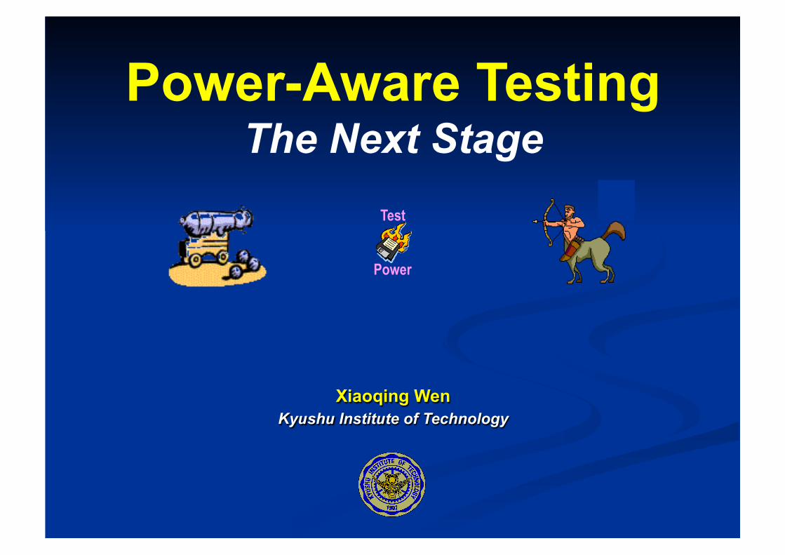
➋
Low-Power Test Coarse-Grained Fine-Grained
Unfocused (Global) Reduction No Test Power Safety Guarantee
Risk of Over-Reduction Power Reduction Only
Risk of Test Quality Degradation Severe Test Data Inflation
Focused (Local) Reduction Guaranteed Test Power Safety
No Over-Reduction Possible Power Increase
Minimum Test Quality Impact Minimum Test Data Inflation
Power-Aware Testing Future Now
Right-Power Test

4 © X. WEN 2012. All Rights Reserved.
Outline
➊ Power: Excitement for Design Engineers
➋ Power: Headach for Test Engineers
➌ Test Power Analysis
➍ Test Power Reduction
➎ Next Stage and New Opportunities
5 © X. WEN 2012. All Rights Reserved.
Outline
➊ Power: Excitement for Design Engineers
➋ Power: Headach for Test Engineers
➌ Test Power Analysis
➍ Test Power Reduction
➎ Next Stage and New Opportunities
6 © X. WEN 2012. All Rights Reserved.
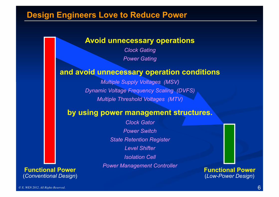
Design Engineers Love to Reduce Power
Avoid unnecessary operations Clock Gating Power Gating
and avoid unnecessary operation conditions Multiple Supply Voltages (MSV)
Dynamic Voltage Frequency Scaling (DVFS) Multiple Threshold Voltages (MTV)
by using power management structures. Clock Gator
Power Switch State Retention Register
Level Shifter Isolation Cell
Power Management Controller
Functional Power (Conventional Design)
Functional Power (Low-Power Design)

7 © X. WEN 2012. All Rights Reserved.
Conventional Design
VDD

8 © X. WEN 2012. All Rights Reserved.
Low-Power Design
VDD2
VDD1
Power Management Structures
Enabled Level Shifter
Isolation Cell
Level Shifter
Power Switch
iso_enable ack req
stop_clock / save / restore
ack
Power Switch
State Retention Register
Power Domain 1 (Conditionally ON)
Power Domain 2 (Always ON)
Power Control Logic
Clock Gator
Clock Gator
Clock Gator
Power Domain 3 (Always ON)

9 © X. WEN 2012. All Rights Reserved.
Outline
➊ Power: Excitement for Design Engineers
➋ Power: Headach for Test Engineers
➌ Test Power Analysis
➍ Test Power Reduction
➎ Next Stage and New Opportunities

10 © X. WEN 2012. All Rights Reserved.
Widening Function-Test Power Gap
Functional Power (Conventional Design)
Test Power Functional Power (Low-Power Design)
Power Management (Hardware) (Software) Excessive
Test Power
Stronger Switching Activity
in Test Mode
Parallelism (faults / blocks)
Non-Functional Test Data
Non-Functional Test Clocking
Excessive Heat • Timing Failures
Test Time / Cost Constraints
Function -Test
Power Gap
Causing Problems Only During Test
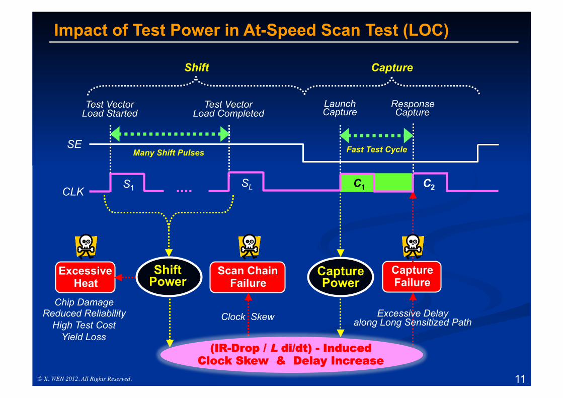
11 © X. WEN 2012. All Rights Reserved.
Scan Chain Failure
Capture Power
(IR-Drop / L di/dt) - Induced Clock Skew & Delay Increase
Excessive Heat
Capture Failure
Launch Capture
C2 C1
Response Capture
Fast Test Cycle
Capture
Shift Power
CLK S1 SL
SE
Test Vector Load Completed
Shift
Test Vector Load Started
Many Shift Pulses
Clock Skew Excessive Delay along Long Sensitized Path
Impact of Test Power in At-Speed Scan Test (LOC)
Chip Damage Reduced Reliability
High Test Cost Yield Loss

12 © X. WEN 2012. All Rights Reserved.
Power Management Structures Add to Test Complexity
VDD2
VDD1
Power Management Structures
(PMS)
PMS-Aware Scan Design
Enabled Level Shifter
Isolation Cell
Level Shifter
Power Switch
iso_enable ack req
stop_clock / save / restore
ack
Power Switch
State Retention Register
Power Domain 1 (Conditionally ON)
Power Domain 2 (Always ON)
Power Control Logic
Clock Gator
Clock Gator
Clock Gator
Power Domain 3 (Always ON)
PMS-Specific DFT Solutions
PMS-Specific Test Generation
13 © X. WEN 2012. All Rights Reserved.
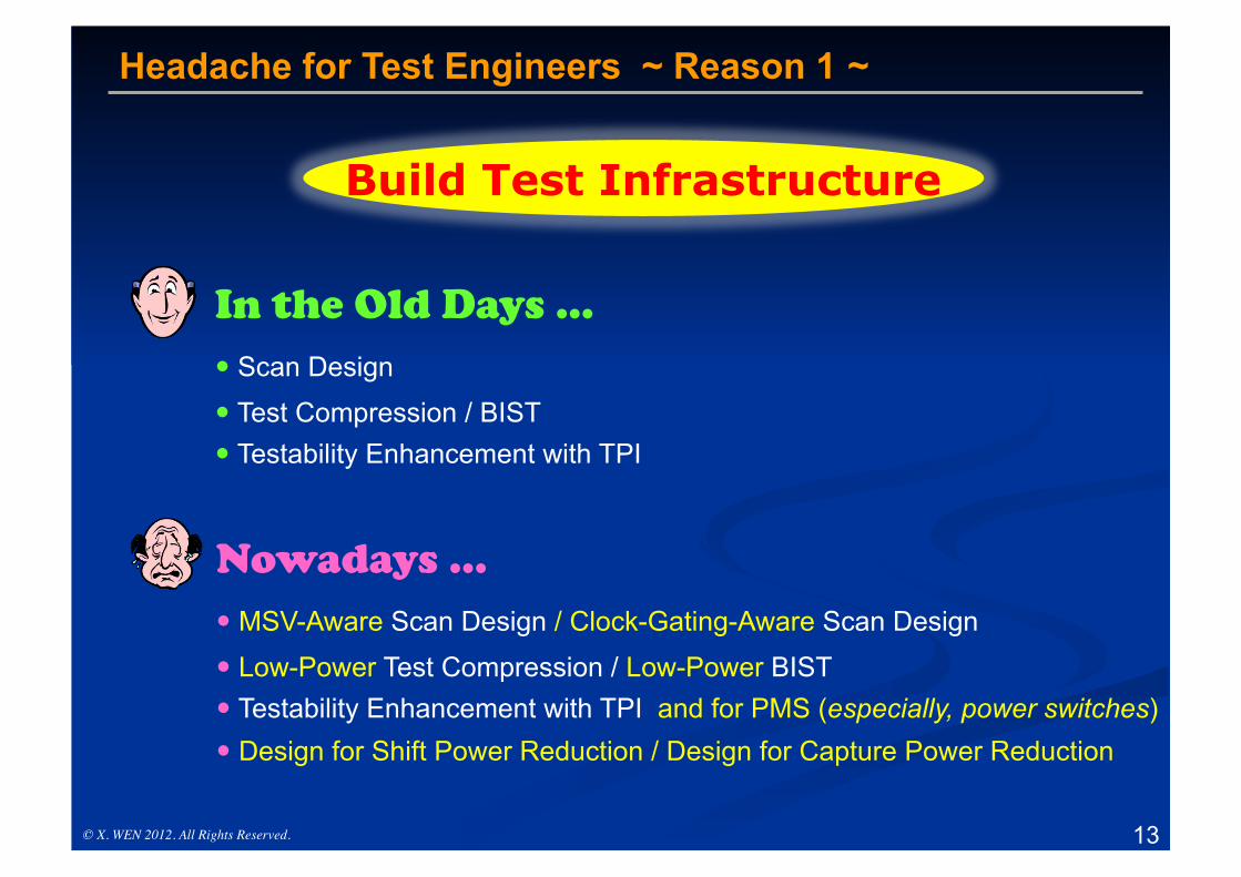
In the Old Days … � Scan Design
� Test Compression / BIST � Testability Enhancement with TPI
Nowadays ... � MSV-Aware Scan Design / Clock-Gating-Aware Scan Design
� Low-Power Test Compression / Low-Power BIST � Testability Enhancement with TPI and for PMS (especially, power switches) � Design for Shift Power Reduction / Design for Capture Power Reduction
Build Test Infrastructure
Headache for Test Engineers ~ Reason 1 ~

14 © X. WEN 2012. All Rights Reserved.
In the Old Days … � Conventional ATPG
Nowadays … Scan Test Power Reduction � Test Power Analysis � Test Power Reduction (low-shift-power ATPG / low-capture-power ATPG) Power-Management-Specific Concerns � System-Level Power-Aware Scheduling due to Limited Power Budget � Test Generation for MSV � Test Generation for Power Management Structures
Prepare Test Data
Headache for Test Engineers ~ Reason 2 ~
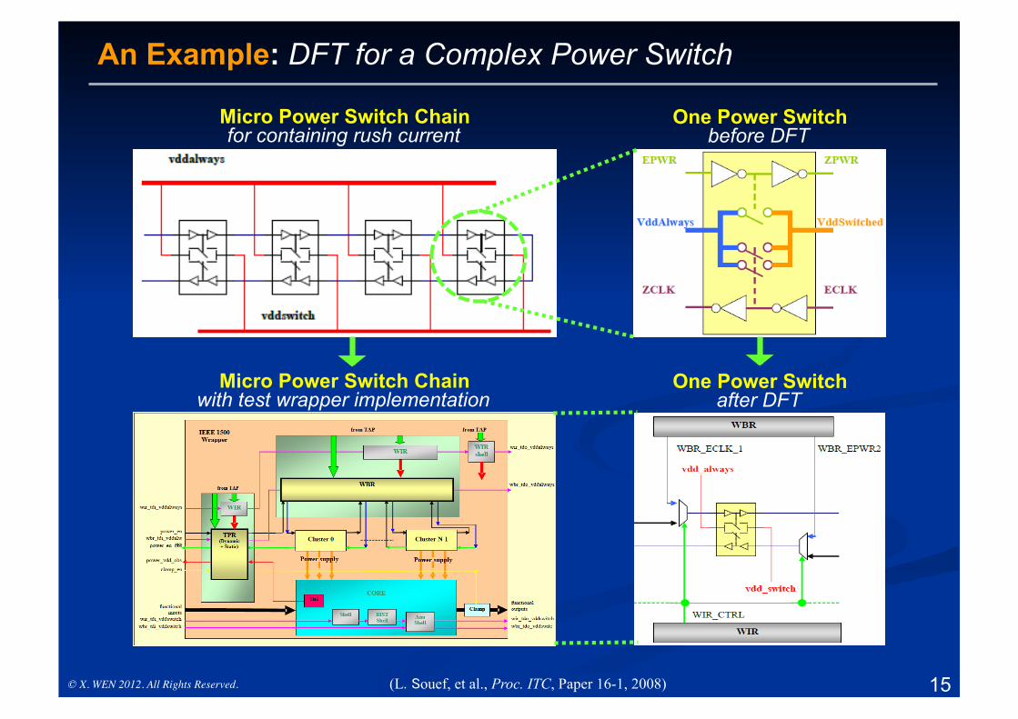
15 © X. WEN 2012. All Rights Reserved. (L. Souef, et al., Proc. ITC, Paper 16-1, 2008)
Micro Power Switch Chain for containing rush current
One Power Switch before DFT
Micro Power Switch Chain with test wrapper implementation
One Power Switch after DFT
An Example: DFT for a Complex Power Switch

16 © X. WEN 2012. All Rights Reserved.
Functional Power
Test Power (without power-aware test)
Function -Test Power Gap
Basic Tasks in Handling Function-Test Power Gap
Test Power Analysis Test Power Reduction
Test Power (with power-aware test)

17 © X. WEN 2012. All Rights Reserved.
Outline
➊ Power: Excitement for Design Engineers
➋ Power: Headach for Test Engineers
➌ Test Power Analysis
➍ Test Power Reduction
➎ Next Stage and New Opportunities

18 © X. WEN 2012. All Rights Reserved.
Temp. Analysis
Sensitization Analysis
Excessive Heat Excessive Delay along Sensitized Paths
Delay Analysis
IR-Drop Analysis +
Ideal vs. Reality
Switching Activity
� Accurate but costly. � OK for sign-off but bad for use in DFT / ATPG.
� Fast and accurate-enough approximation needed. � Gate-level metric preferred.
Ideal Reality
Global Local

19 © X. WEN 2012. All Rights Reserved.
SFF2 SFF4 SFF1 SFF3 SI SO
Global Analysis Shift Power
Weighted_Transitions = ∑ (Scan_Chain_Length - Transition_Position)
(R. Sankaralingam, et al., Proc. VTS, pp. 35-40, 2000)
0 1 1 0
0 - - -
1 0 - - 1 1 0 - 0 1 1 0
4 3 2 1 T1
T2
T3
T4

20 © X. WEN 2012. All Rights Reserved.
B19 ITC'99 Benchmark (196K Gates) 160 Test Vectors → WSAave = 47.7%
Risky Test Vectors: Ta, Tb → WSA(Ta) = 44.8% / WSA(Tb) = 46.7%
Global Analysis
Toggle Count ∑ transitions with weight of 1
Weighted Switching Activity (WSA) ∑ transitions with weight of fanout (+1)
Capture Power Whole Circuit
Individual Block
FFs Only
All Nodes
?
21 © X. WEN 2012. All Rights Reserved.
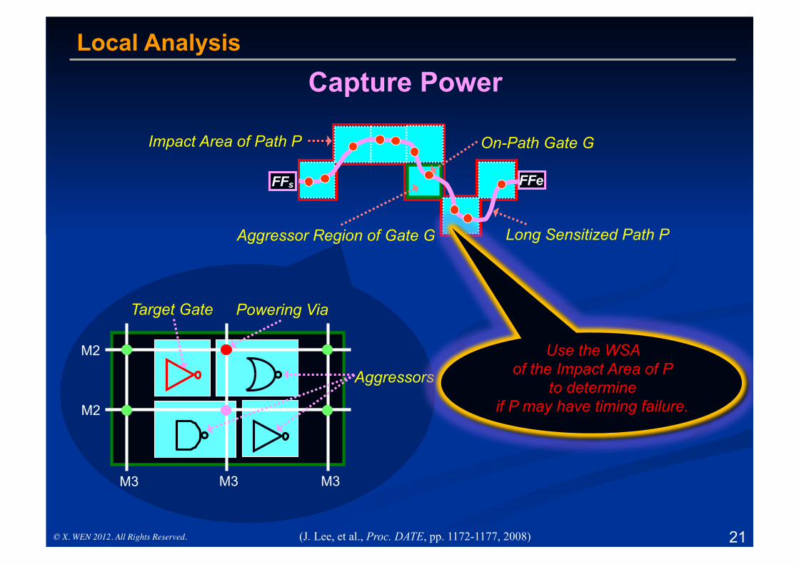
Aggressor Region of Gate G
On-Path Gate G
Long Sensitized Path P
Impact Area of Path P
M2
M2
M3 M3 M3
Powering Via Target Gate
Aggressors
Use the WSA of the Impact Area of P
to determine if P may have timing failure.
FFs FFe
Local Analysis Capture Power
(J. Lee, et al., Proc. DATE, pp. 1172-1177, 2008)
22 © X. WEN 2012. All Rights Reserved.
Outline
➊ Power: Excitement for Design Engineers
➋ Power: Headach for Test Engineers
➌ Test Power Analysis
➍ Test Power Reduction
➎ Next Stage and New Opportunities
23 © X. WEN 2012. All Rights Reserved.
Basic Strategies
Shift Power Reduction
Capture Power Reduction

24 © X. WEN 2012. All Rights Reserved.
Basic Strategies
25 © X. WEN 2012. All Rights Reserved.
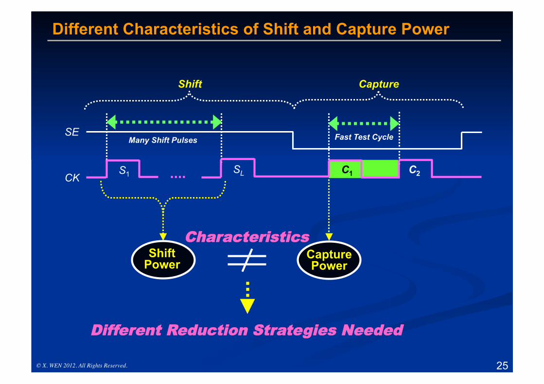
Different Characteristics of Shift and Capture Power
Capture Power
S1 C2 C1 SL CK
SE Fast Test Cycle
Shift Capture
Shift Power
Many Shift Pulses
Different Reduction Strategies Needed
Characteristics
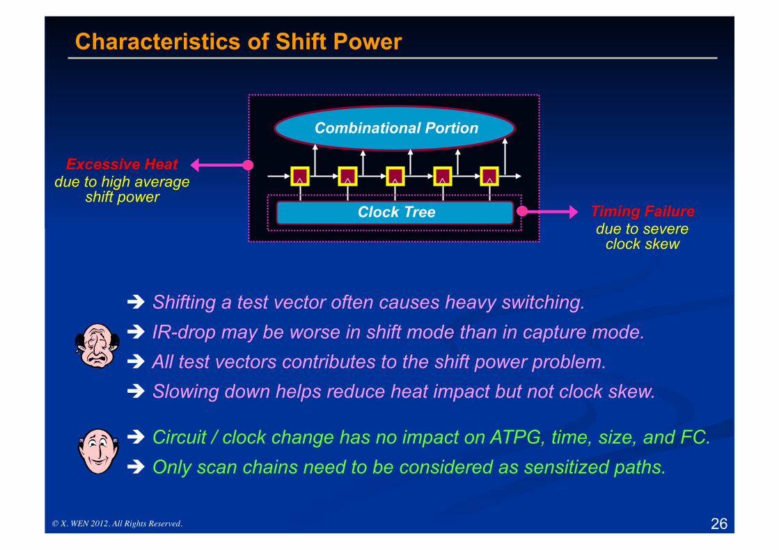
26 © X. WEN 2012. All Rights Reserved.
Combinational Portion
Clock Tree
Excessive Heat due to high average
shift power Timing Failure due to severe
clock skew
è Shifting a test vector often causes heavy switching. è IR-drop may be worse in shift mode than in capture mode. è All test vectors contributes to the shift power problem. è Slowing down helps reduce heat impact but not clock skew.
è Circuit / clock change has no impact on ATPG, time, size, and FC. è Only scan chains need to be considered as sensitized paths.
Characteristics of Shift Power

27 © X. WEN 2012. All Rights Reserved.
Timing Failure due to excessive delay
increase along long sensitized paths
è Capture power mostly impacts sensitized paths. è Reducing capture power may be needed to avoid yield loss. è Circuit / clock change may impact ATPG, time, size, and FC.
è Capture power depends on the content of a test vector. è A small portion of test vectors suffers from excessive capture power. è Increasing capture power may help to improve test quality. è Power management circuitry helps reduce capture power.
Combinational Portion
Clock Tree
Sensitized Path Better SDD Coverage
due to proper delay Increase along
short sensitized paths
Characteristics of Capture Power
28 © X. WEN 2012. All Rights Reserved.
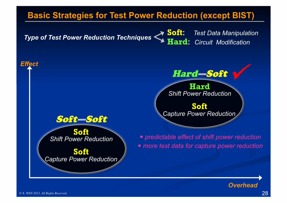
Effect
Overhead
Soft Shift Power Reduction
Soft
Capture Power Reduction
Hard Shift Power Reduction
Soft
Capture Power Reduction
Soft: Test Data Manipulation Hard: Circuit Modification
Type of Test Power Reduction Techniques
Soft—Soft
Hard—Soft ü
Basic Strategies for Test Power Reduction (except BIST)
� predictable effect of shift power reduction � more test data for capture power reduction
29 © X. WEN 2012. All Rights Reserved.
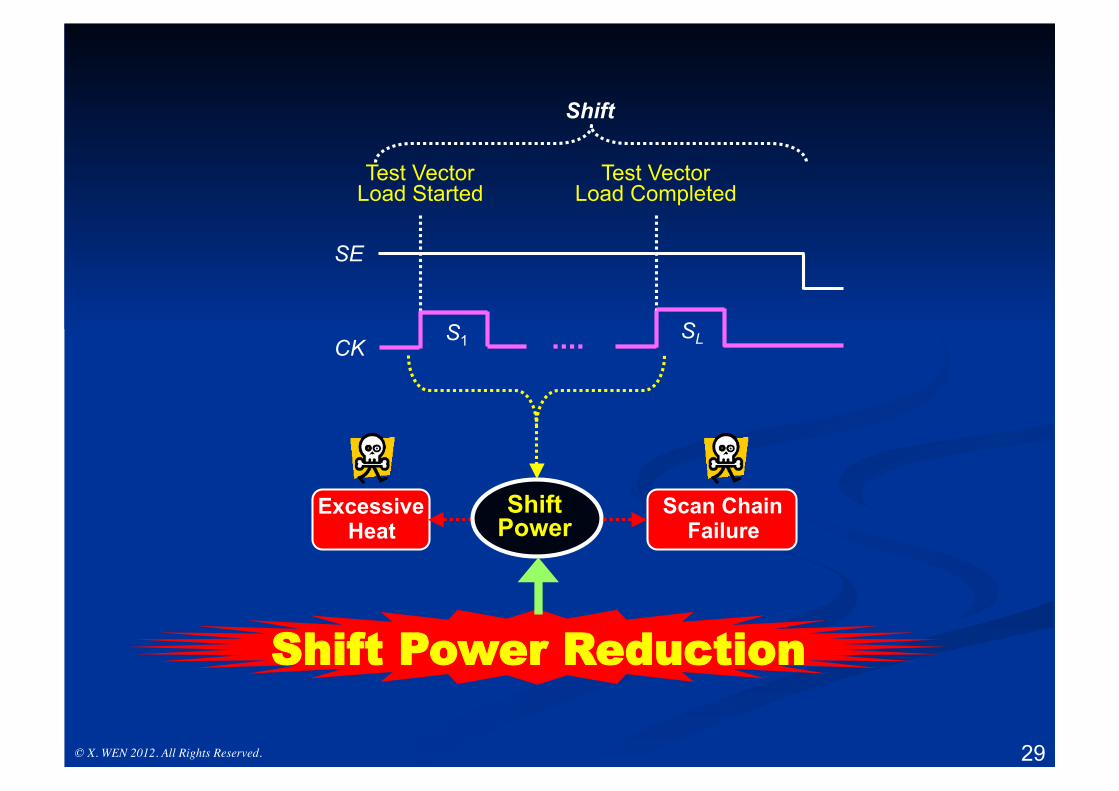
Scan Chain Failure
Excessive Heat
S1 SL CK
SE
Test Vector Load Completed
Test Vector Load Started
Shift Power
Shift Power Reduction
Shift

30 © X. WEN 2012. All Rights Reserved.
Scan Segmentation
Predictable and data-independent shift (in & out) power reduction. No change to ATPG and no increase in test application time.
(L. Whetsel, Proc. ITC, pp. 863-872, 2000)
scan chain division 1 0
1scan chain division 2
scan input scan
output
clock
control for scan clock and
scan output
...
...
...
captureshift division 2shift division 1 shift
......
Original Scan Chain
Normal Scan Compressed Scan

31 © X. WEN 2012. All Rights Reserved.
Capture Power
C2 C1
Launch Capture
Response Capture
Test Cycle
Capture
Capture Failure
Capture Power Reduction
32 © X. WEN 2012. All Rights Reserved.
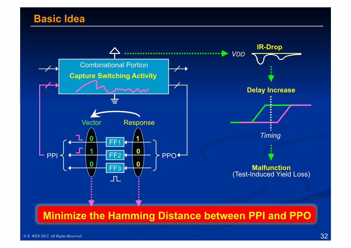
Basic Idea
0
1
1
0
0 0
Vector Response
Combinational Portion
FF1
FF2
FF3
PPI PPO
Capture Switching Activity
IR-Drop
Delay Increase
Malfunction (Test-Induced Yield Loss)
VDD
Timing
Minimize the Hamming Distance between PPI and PPO
33 © X. WEN 2012. All Rights Reserved.
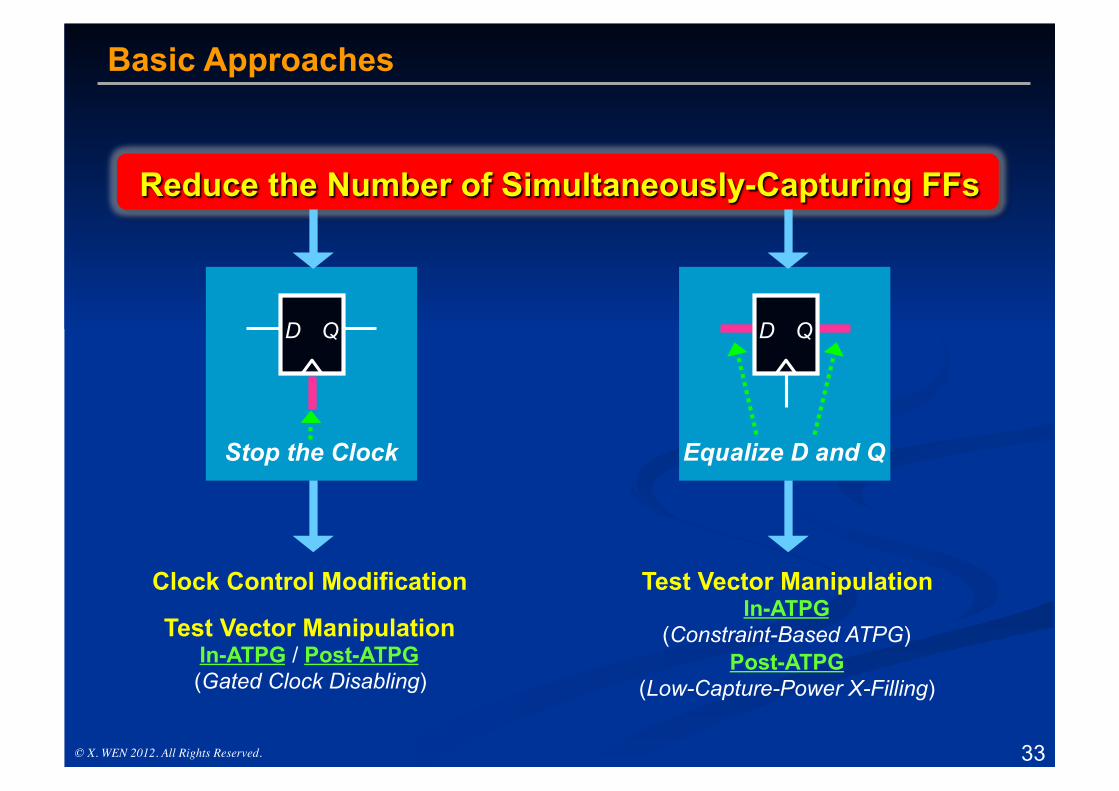
Basic Approaches
Reduce the Number of Simultaneously-Capturing FFs
Clock Control Modification
D Q
Stop the Clock
D Q
Equalize D and Q
Test Vector Manipulation In-ATPG / Post-ATPG (Gated Clock Disabling)
Test Vector Manipulation In-ATPG
(Constraint-Based ATPG) Post-ATPG
(Low-Capture-Power X-Filling)

34 © X. WEN 2012. All Rights Reserved.
(Low Capture Power)
Combinational Portion
FF1
FF2 PPI PPO
0 0
1 0
Assign logic values for X-bits so that PPI = PPO.
LCP X-Filling
a b c 1 1 1 1 1 1 0 1 1
v1 v2 v3
Compact Test Set
a
b
c
f
g
d
e
(High Capture Power)
Initial Test Generation
Test Cube Set
Find X-bits (No / Recoverable FC Loss)
a b c 1 1 X 1 X 1 X 1 X
v1 v2 v3
Dynamic Compaction (Random-Filling)
a b c 1 1 0 1 0 1 0 1 0
v1 v2 v3
Compact Test Set
X-Identification X-Restoration
Easy to implement. No or little test data increase.
An Example: Processing Flow
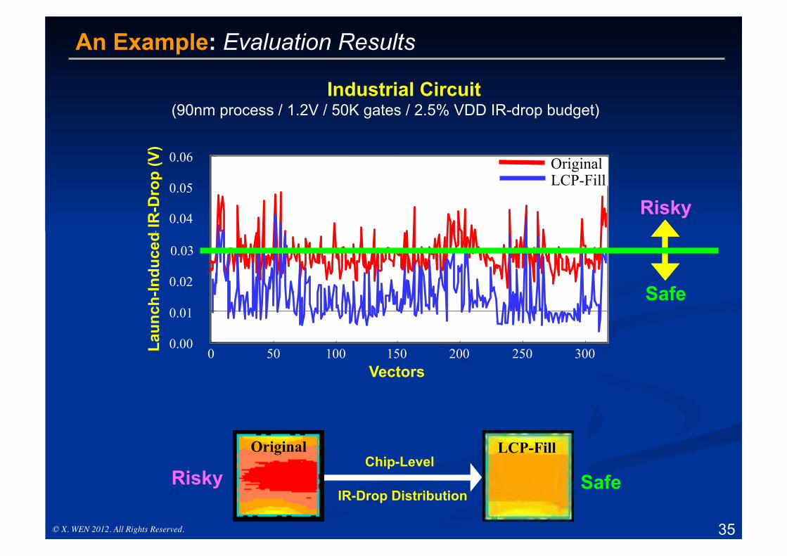
35 © X. WEN 2012. All Rights Reserved.
Industrial Circuit (90nm process / 1.2V / 50K gates / 2.5% VDD IR-drop budget)
0.00
0.01
0.02
0.03
0.04
0.05
0.06
0 50 100 150 200 250 300 Vectors .
- Original LCP-Fill
Laun
ch-In
duce
d IR
-Dro
p (V
)
Risky
Safe
Risky
Safe
LCP-Fill Original Chip-Level
IR-Drop Distribution
An Example: Evaluation Results
36 © X. WEN 2012. All Rights Reserved.
Outline
➊ Power: Excitement for Design Engineers
➋ Power: Headach for Test Engineers
➌ Test Power Analysis
➍ Test Power Reduction
➎ Next Stage and New Opportunities

37 © X. WEN 2012. All Rights Reserved.
Ultimate Goals in Power-Aware Testing
Test Quality
Test Cost
Test Power
Guaranteed Test Power Safety
Uncompromised Test Quality
Minimized Test Cost Impact
38 © X. WEN 2012. All Rights Reserved.
Current Problems
39 © X. WEN 2012. All Rights Reserved.
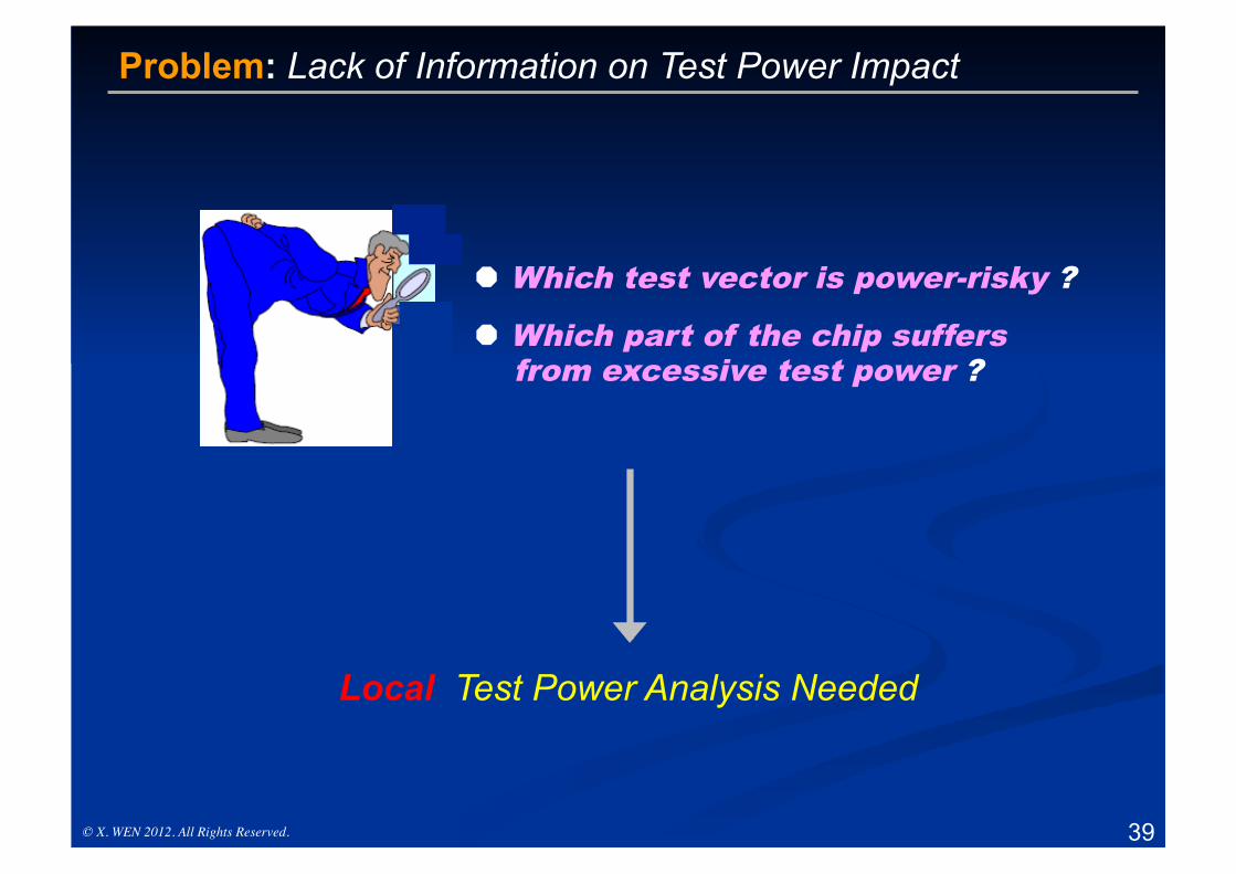
Problem: Lack of Information on Test Power Impact
Local Test Power Analysis Needed
Ä Which test vector is power-risky ? Ä Which part of the chip suffers from excessive test power ?

40 © X. WEN 2012. All Rights Reserved.
Problem: Clock Skew during Scan Shift
Clock Tree
Combinational Portion
Excessive Heat
Excessive Clock Skew
Good Solutions
Local Shift Power Management Needed

41 © X. WEN 2012. All Rights Reserved.
Long Sensitized Path Switching Gate Non-Switching Gate
Global Test
Power Reduction
Long Sensitized Path
Still Risky !
Circuit # of Gates
# of FFs
# of Clock Gators
# of Test Vectors
Test Power Analysis
# of Risky Test
Vec.
Ave. Sens. Paths / Vec.
Ave. Risky. Paths / Vec.
CPU (sec.)
# of Risky Vec. with Low WSA
Small 50K 1,077 66 319 8 0.1 1.1 48 3
Large 600K 35,566 984 191 11 0.2 3.8 2,772 5
Problem: Low-Power ≠ Power-Safe during Scan Capture
Local Capture Power Management Needed
42 © X. WEN 2012. All Rights Reserved.
Next Stage
43 © X. WEN 2012. All Rights Reserved.
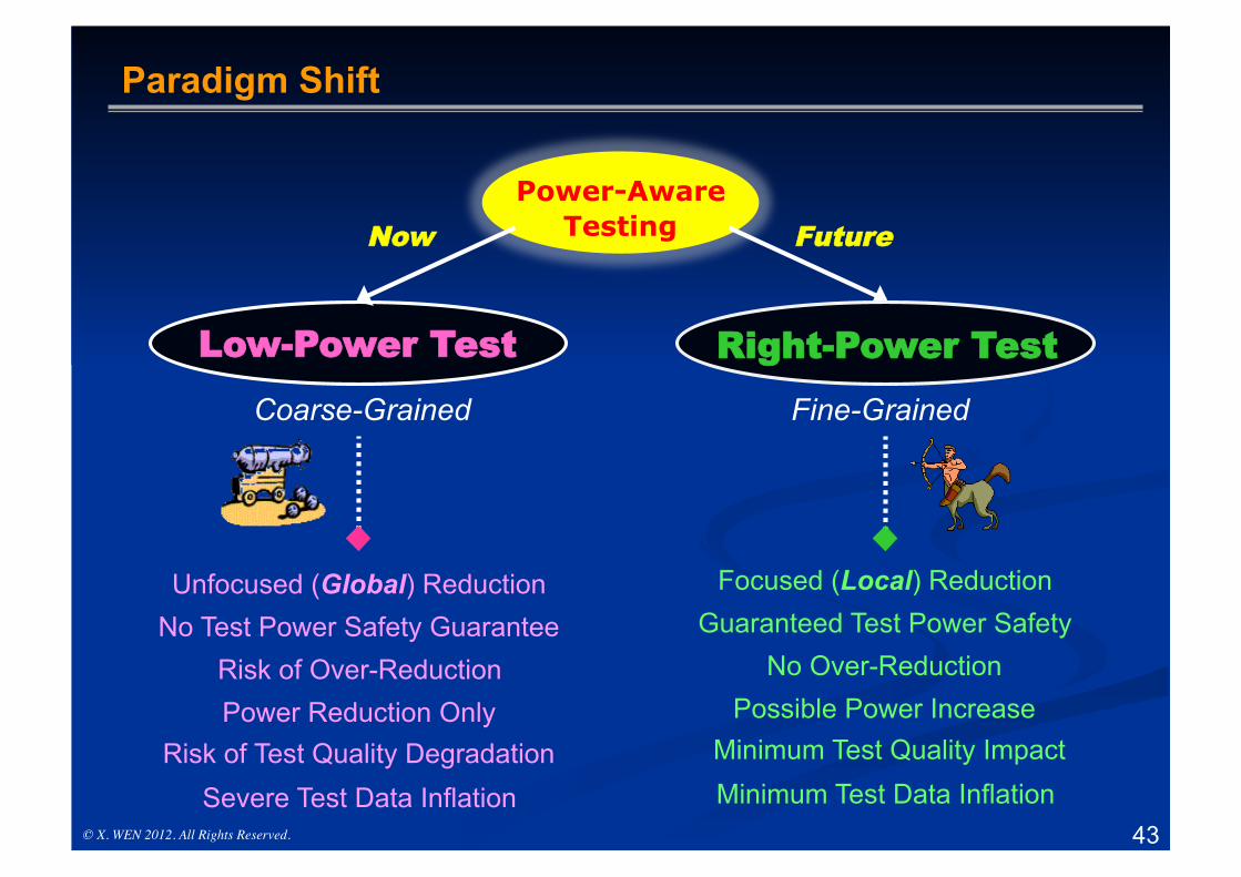
Low-Power Test Coarse-Grained Fine-Grained
Unfocused (Global) Reduction No Test Power Safety Guarantee
Risk of Over-Reduction Power Reduction Only
Risk of Test Quality Degradation Severe Test Data Inflation
Focused (Local) Reduction Guaranteed Test Power Safety
No Over-Reduction Possible Power Increase
Minimum Test Quality Impact Minimum Test Data Inflation
Power-Aware Testing Future Now
Right-Power Test
Paradigm Shift

44 © X. WEN 2012. All Rights Reserved.
Some Interesting R&D Topics (in random order)
Ä Power-Aware 3D Testing
Ä Power-Aware FPGA Testing
Ä Power-Aware On-Line Testing
Ä Low-Overhead Power-Safe BIST
Ä Right-Shift-Power Test Generation
Ä Power-Aware Fault Tolerance Design
Ä Right-Capture-Power Test Generation
Ä Fast and Accurate Power Safety Checking
Ä System-Level Power-Aware Test Scheduling
Ä Low-Overhead Power-Safe Scan Test Compression
Ä Fault Diagnosis and Silicon Debug of Low-Power Circuits
Ä IP with Power-Aware Test Infrastructure and Right-Power Test Data
Ä Seamless Power-Aware DFT based on CPF or UPF (IEEE Std. 1801-2009)

45 © X. WEN 2012. All Rights Reserved.
Some Interesting R&D Topics (in random order)
Ä Power-Aware 3D Testing
Ä Power-Aware FPGA Testing
Ä Power-Aware On-Line Testing
Ä Low-Overhead Power-Safe BIST
Ä Right-Shift-Power Test Generation
Ä Power-Aware Fault Tolerance Design
Ä Right-Capture-Power Test Generation
Ä Fast and Accurate Power Safety Checking
Ä System-Level Power-Aware Test Scheduling
Ä Low-Overhead Power-Safe Scan Test Compression
Ä Fault Diagnosis and Silicon Debug of Low-Power Circuits
Ä IP with Power-Aware Test Infrastructure and Right-Power Test Data
Ä Seamless Power-Aware DFT based on CPF or UPF (IEEE Std. 1801-2009)

46 © X. WEN 2012. All Rights Reserved.
An Example: Right-Capture-Power Test
Pinpoint Capture Power
Management
Long Sensitized Path
Sensitized Path
Non-Sensitized Path
FFs V F (V)
Capture
High Local Switching Activity
Low Local Switching Activity
Cold
Hot
Dead
No need to consider dead areas. Hot areas must be removed by reducing local switching. Cold areas may be made “warm” by increasing local switching.

47 © X. WEN 2012. All Rights Reserved.
48 © X. WEN 2012. All Rights Reserved.
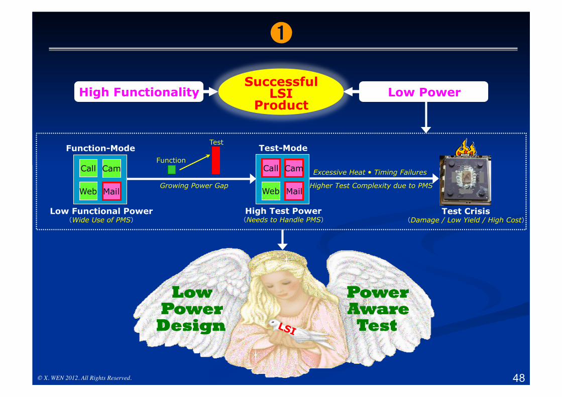
High Functionality
Call Cam
Web Mail
Function-Mode
Low Functional Power (Wide Use of PMS)
Successful LSI
Product Low Power
Call Cam
Web Mail
Test-Mode
High Test Power (Needs to Handle PMS)
Function
Test
Growing Power Gap
Test Crisis (Damage / Low Yield / High Cost)
Excessive Heat � Timing Failures
Low Power
Design
Power Aware
Test
➊
Higher Test Complexity due to PMS

49 © X. WEN 2012. All Rights Reserved.
➋
Low-Power Test Coarse-Grained Fine-Grained
Unfocused (Global) Reduction No Test Power Safety Guarantee
Risk of Over-Reduction Power Reduction Only
Risk of Test Quality Degradation Severe Test Data Inflation
Focused (Local) Reduction Guaranteed Test Power Safety
No Over-Reduction Possible Power Increase
Minimum Test Quality Impact Minimum Test Data Inflation
Power-Aware Testing Future Now
Right-Power Test

50 © X. WEN 2012. All Rights Reserved.
THANK YOU
Let us make LSI test cool.