Embed Size (px)
Citation preview

15
Potential of Grid Technology for Embedded Systems and Applications
Mona Abo El-Dahb1,2 and Yoichi Shiraishi2 1Department of Computer Science,
Faculty of Engineering, Helwan University, Cairo, 2Department of Production Science and Technology,
Graduate School of Engineering, Gunma University, 1Egypt 2Japan
1. Introduction
First, this chapter offers a brief introduction for the grid computing and its potential in the
embedded system design, embedded system definition the difference between the
embedded system and the general purpose computer, embedded systems classification and
the design challenges. Next, an embedded system design for inverter power supply is
described as a case study. An embedded system can be simply defined as a combination of
hardware (microprocessor) and software that is built into a product for purposes such as
controlling, monitoring and communication without human intervention. Furthermore,
embedded system is a special-purpose computing device designed to perform dedicated
functions. The hardware includes a microprocessor or microcontroller with additional
external memory, I/O, and other components such as sensors, keypad, LEDs, LCDs, and
any kind of actuators. The embedded software is the driving force of the embedded system
design. Once it is loaded, the embedded software will never be changed unless it needs to be
reloaded or replaced (Turley, 2010 & Henzinger and Sifakis, 2006 & Hongxing and Thomas,
2006). Nowadays, embedded systems can be found in devices ranging from from digital
watches to communication systems, transportation navigation systems, medical systems,
and financial systems. Figure 1 shows some examples of the applications of embedded
systems. The number of the embedded systems has increased rapidly in the last few decades
to meet modern life demands.
2. Embedded system versus general-purpose system
An embedded system is usually classified as a system that has a set of predefined, specific functions to be performed and in which the resources are constrained (Stepner et al., 1999). For example, the mobile phone is an embedded system and it has several readily apparent functions as follows: the main function is to call and receive phone calls, along with perhaps several other functions such as a stopwatch, time-keeper, alarm, and camera and so on. A mobile phone also has several resource constraints as follows: firstly, the processor that is
www.intechopen.com

Grid Computing – Technology and Applications, Widespread Coverage and New Horizons
326
Fig. 1. Examples of embedded system
operating the mobile phone cannot be very large, or else no one would use it. Secondly, the power consumption must be minimal as only a small battery can be contained in a mobile phone. Finally, it must perform its function accurately. Each embedded system design satisfies its own set of functions and constraints. By comparing this example with the general propose computer we can see the differences. In this section, the main differences between both systems are described below:
1. Embedded systems are dedicated to specific tasks, where PCs are general computing platforms. An embedded system is programmed to perform specific tasks. Conversely, a general-purpose computer is able to perform unlimited tasks or one can install any software to do all kinds of tasks such as word processing, data sheet, database management, and others depending on one’s purposes.
2. Embedded systems are usually cost-sensitive because the embedded system is only part of the whole product. Subsequently, if the cost of the embedded system reduces, one can potentially reduce the product cost.
3. The implication of software failure are much more severe in the embedded systems than the general propose computer. It is considered one of the most difficult technical and commercial environments because many critical systems are controlled by the embedded computer system. These include communication systems, transportation navigation systems, medical systems, and financial systems. Failure or compromise of such a system can have significant consequences including disruption of critical services, financial loss, and loss of life (Thomas, 2006).
4. Embedded systems have power constrains. This is not a practically serious constraint for the general-purpose computer system. However, consider an embedded system connected to medical system in the ambulance, so the system must work reliably and for a long time with a set of small batteries. So, it is very important issue to keep the embedded system running on a minute amount of power (Berger, 2002).
www.intechopen.com

Potential of Grid Technology for Embedded Systems and Applications
327
5. Embedded systems have real-time constraints. Real-time constraints generally are grouped into categories depending on the application as follows: the first category is time-sensitive constraints and; the second category is time-critical constraints. If the application has time-critical constraints the task must take place within a set window of time, controlling the flight worthiness of an aircraft is a good example of this.
6. Embedded systems must operate under different environmental conditions. The embedded systems are everywhere, so the system must be designed to work well in different environment conditions and in the harsh environment as well.
7. Embedded systems microprocessors often have debugging circuitry.
3. Challenges of embedded software design
Embedded system development tools have traditionally lagged behind tools for the
development of general systems (ChristopherChristopher, 2000). Unlike general systems,
the design space for embedded systems is extremely large, so it is difficult to contain all of
the facilities to specify, design, and test embedded systems. The number of embedded
systems increased rapidly year by year and then the designers of the embedded system face
ever-increasing challenges in the design stage. Some of these challenges are listed below:
1. In the traditional design method of the embedded system, the hardware and the software of an embedded system are developed simultaneously, which is a sharp contrast to the general or business system. In the business system development, the hardware on which the software should be executed is available. Usually in the business software development, the software can be tested and modified in the computer. However, in the embedded software design, even the specifications of hardware are generally not completed. Therefore, embedded software cannot test on the actual platform until the completion of the hardware. This will cause the degradations of qualities of embedded software as well as increasing the process time (Woodward and Mosterman, 2007).
2. In the traditional development method, design took places early in the development process, and the software designer should wait until late in the process. Then the embedded software is tested in the actual prototype. So, revealing the errors in the embedded software is considered a critical step. Furthermore, the discovery of errors often resulted in production delay as well as the possibility of additional expenses to the product cost (Woodward and Mosterman, 2007 & Manfred, 2006).
3. One of the major challenges in the design process of embedded systems is to accurately predict performance characteristics of the final system implementation in the early design stages.
4. The complexity of the embedded system arises due to the combination of more and
more functions onto a single system (Woodward and Mosterman, 2007 & Madhukar
and Lee, 2008). For example, luxury vehicles produced today contain more than 90
embedded electronic control units (ECU), which execute more than 10 million lines of
computer codes that control many different functions in a car (Ming-Shan, 2007).
Increase of system complexity may also lead to the increase of a project time and the
system design cost.
5. As aforementioned, the main difference between the conventional computer systems and the embedded computer systems is that the hardware on which the software
www.intechopen.com
Grid Computing – Technology and Applications, Widespread Coverage and New Horizons
328
should be executed is unavailable. Therefore, a simulator of the embedded hardware is very useful for the development of the embedded software but it becomes a difficult matter because of the length of time required to build a simulator (Woodward and Mosterman, 2007 & Madhukar and Lee, 2008).
6. Verification is the process of determining whether a system satisfies a given property of interest or not. It is considered one of the most difficult challenges of the embedded system. Due to the fact that the embedded systems deal with very critical applications, a designer has to make sure that the system meets the required specification perfectly. It is reported that the verification takes more than 50 to 70% of the project time and the cost for verification of the embedded system is increasing rapidly (Christopher, 2000).
7. As a result, the competition among the companies to deliver the product to the market faster and with lower cost. In most cases, the embedded system is a part of the system. Thus, any delay in the embedded system development will cause overall delay in the project or products.
However, nowadays, embedded systems have garnered more interests in the research community, as well as there being an increased need for those embedded systems. The increase of the embedded system challenges opens a wide range of research in the development tools. Most of researchers try to find a design tool that can solve some of the challenges of embedded system design. Model Based Design method is one of the techniques for developing embedded software and it puts a system model at the center of the developing processes. For example, the environment supplied by MathWorks, Inc. allows engineers to mathematically model the behaviors of the physical system and re-use the program components in the library. This approach meets with significant success in some applications. This chapter will investigate the development of the inverter power supply as an example of the embedded system. The embedded software of the inverter power supply is optimized and tested using the Model Based Design (MBD) method. Moreover, the superiority of this method to the traditional design method is verified.
4. Grid technology for embedded system and application
Grid computing is another way of distributed computing. Distributed computing is a science which solves a large problem by giving small parts of the problem to many computers to solve and then combining the solutions for the parts into a solution for the problem. Grid Computing finds many potential opportunities and advantages in the fields of education, research, engineering, bio-medicine, pharmaceuticals, financial sector and government organizations(Mark,el.,2002). In the embedded system design the gird computing technology is used for improving the developing cycle of the embedded system . for example, GridSim is a toolkit for modeling and simulation of Grid resources and application scheduling. It provides a comprehensive facility for the simulation of different classes of heterogeneous resources, users, applications, resource brokers, and schedulers. It has facilities for the modeling and simulation of resources and network connectivity with different capabilities, configurations, and domains. It supports primitives for application composition, information services for resource discovery, and interfaces for assigning application tasks to resources and managing their execution. These features can be used to simulate resource brokers or Grid schedulers to evaluate performance of scheduling algorithms or heuristics(Buyya R, el.,2002). May programs are built based on the gird technology one of this program is the MATLAB and SimuLink which is used in this study.
www.intechopen.com
Potential of Grid Technology for Embedded Systems and Applications
329
MATLAB is a high-level technical computing language and interactive environment for
algorithm development, data visualization, data analysis, and numeric computation. The
MATLAB infrastructure design is based on the gird computing technology .MATLAB is
used to solve problems in several application areas such as signal and image processing,
communications, control design, test and measurement, financial modeling and analysis,
and computational biology. Add-on toolboxes extend the MATLAB environment to solve
particular classes of problems in different application areas.
Simulink is a companion product to MATLAB that offers an environment for multidomain
simulation and Model-Based Design for dynamic and embedded systems. It provides an
interactive graphical environment and a customizable set of block libraries that allows users
to design, simulate, implement, and test a variety of time-varying systems.
In this chapter we used the Model Based Design method to eliminate some of the embedded
system challenges. Model Based Design is a simulation based method so, if the embedded
system becomes large and more complicated, its simulation time will be increased. To
accelerate the simulation time of such embedded systems, some parallel and distributed
systems (grid computing method) are necessary.
5. Model based design
Currently, many researches are focused on determining a good way to eliminate the
challenges of the embedded systems design. Embedded systems have particularly tight
performance, time to market and cost constraint. To meet these constraints, researchers try
to find solutions to efficiently design the systems with required performances. Recently, the
MBD method is considered to be one of the chief techniques in this field. The Model Based
Design method is considered one of the leading techniques as a solution of those challenges.
In this method, the model can be used to verify the plant design and the control algorithm.
MBD method puts a system model at the center of the development process, from
requirement development through design implementation (Woodward and Mosterman,
2007).
The system specifications phase is started by the analysis and the documentation of the
system requirements. In the traditional method, this step is accomplished using the paper-
based method which results in poor communication in the design process, errors in the
design as well as limited traceability between the design and the requirements. In the MBD
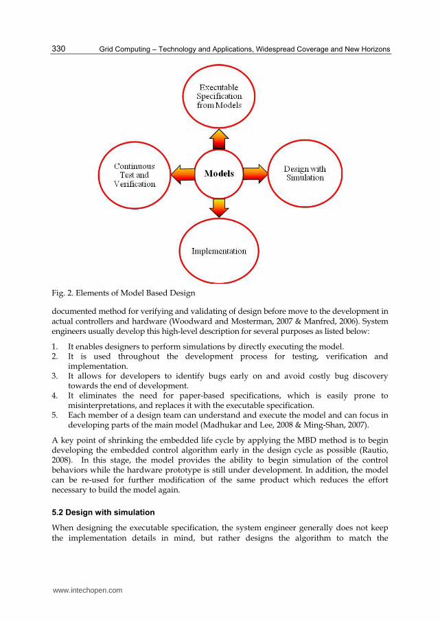
method, the model can provide an excellent virtual environment for high level descriptions
of the embedded system, as shown in Figure 2. This figure illustrates the main four elements
of the MBD method. The description for elements of Model Based Design method is
presented below.
5.1 Executable specifications
As designs become larger and more complicated, it becomes necessary to first describe them at a high level of abstraction. For example, Simulink (The MathWork web site) can provide specific block-sets such as signal processing, communication, video and image processing block set to help the designer to build an abstraction model. This model provides a
www.intechopen.com
Grid Computing – Technology and Applications, Widespread Coverage and New Horizons
330
Fig. 2. Elements of Model Based Design
documented method for verifying and validating of design before move to the development in actual controllers and hardware (Woodward and Mosterman, 2007 & Manfred, 2006). System engineers usually develop this high-level description for several purposes as listed below:
1. It enables designers to perform simulations by directly executing the model. 2. It is used throughout the development process for testing, verification and
implementation. 3. It allows for developers to identify bugs early on and avoid costly bug discovery
towards the end of development. 4. It eliminates the need for paper-based specifications, which is easily prone to
misinterpretations, and replaces it with the executable specification. 5. Each member of a design team can understand and execute the model and can focus in
developing parts of the main model (Madhukar and Lee, 2008 & Ming-Shan, 2007).
A key point of shrinking the embedded life cycle by applying the MBD method is to begin developing the embedded control algorithm early in the design cycle as possible (Rautio, 2008). In this stage, the model provides the ability to begin simulation of the control behaviors while the hardware prototype is still under development. In addition, the model can be re-used for further modification of the same product which reduces the effort necessary to build the model again.
5.2 Design with simulation
When designing the executable specification, the system engineer generally does not keep the implementation details in mind, but rather designs the algorithm to match the
www.intechopen.com
Potential of Grid Technology for Embedded Systems and Applications
331
behavioral requirements for the system. Once the system engineer submits the executable specification to the development team, the team may need to make modifications to it in order to fit the design into a real world that may have limited resources, such as memory or processing power. These modifications may cause the output of the new design to deviate from the original design. Design engineers should decide if the deviation is acceptable. In this section, modifications in the controlling algorithms will be done to make it suitable for hardware implementation and demonstrate how to continuously verify the design against the executable specifications. For example, if the designers need to change the controlling algorithm to meet the requirements, MBD method provides an environment where the designer can redesign the control algorithms and validate it in very short time comparing to traditional method of design (Ming-Shan, 2007).
5.3 Implementation and testing
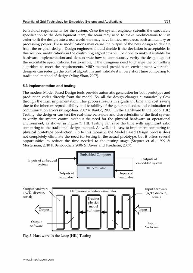
The modern Model Based Design tools provide automatic generation for both prototype and production codes directly from the model. So, all the design changes automatically flow through the final implementation. This process results in significant time and cost saving due to the inherent reproducibility and testability of the generated codes and elimination of communication errors (Ming-Shan, 2007 & Rautio, 2008). In the Hardware In the Loop (HIL) Testing, the designer can test the real-time behaviors and characteristics of the final system to verify the system control without the need for the physical hardware or operational environment, as shown in Figure 3. HIL Testing can save the time with significant ratio comparing to the traditional design method. As well, it is easy to implement comparing to physical prototype production. Up to this moment, the Model Based Design process does not completely eliminate the need for testing in the actual prototype, but it offers several opportunities to reduce the time needed to the testing stage (Stepner et al., 1999 & Mosterman, 2010 & Behboodian, 2006 & Davey and Friedman, 2007).
Fig. 3. Hardware In the Loop (HIL) Testing
Output hardware (A/D, discrete, serial)
Input Software
Input
Hardware-in-the-loop-simulator
Truth or physics model
softwareOutput
Input hardware (A/D, discrete,
serial)
Output Software
Outputs of embedded system
Inputs of simulator
Outputs of simulator
Inputs of embedded system
Embedded Computer
HIL Simulator
www.intechopen.com

Grid Computing – Technology and Applications, Widespread Coverage and New Horizons
332
Generally, it can be concluded that the Model Based Design method will reduce the number of the development stages by combining the design, implementation and testing into one process. The reduction of the required step comparing to the traditional method of design will result in better project management and mitigate the system development risk. The system design using this approach will reach the market faster and will cost less than that of the system designed using the traditional method. Subsequently, the use of the MBD method can provide numerous advantages over the traditional design method. Therefore, this study investigates how the Model Based Design method can provide such advantages by applying and building a new virtual environment for the embedded system design. Inverter power supply is used as a case study of the embedded system in this research.
6. Description of the inverter power supply
The development of new useful energy sources is the key to continued industrial progress. Discovering new sources of energy, obtaining an essentially inexhaustible energy source, making it available everywhere and converting it from one form to another without polluting or destroying the environment are some of the great challenges in the world today. One of the techniques to tackle these challenges is to produce AC (Alternative Current) from DC (Direct Current) generated by fuel cells or solar panels and such device is called an inverter power supply. An inverter power supply is a device which can convert DC to AC that can be used in various AC applications. Many topologies are considered to be candidates for the inverter design and there are many factors affecting the choice of such topology, such as the size and the required efficiency as well as the cost of the inverter. In this study, an inverter power supply configuration is broken into two stages. The first stage is to step up the DC voltage level by using DC/DC converter and the second stage is to invert DC to AC through a DC/AC inverter. The block diagram of the inverter power supply is shown in Figure 4.
Fig. 4. Block diagram of inverter power supply
Analog Signals
DC/DC Circuit DC/AC Circuit
Microprocessor Control Circuit
Digital Signals
www.intechopen.com
Potential of Grid Technology for Embedded Systems and Applications
333
In this application, the operation of the electric circuit is controlled by the embedded system
that includes the SH microprocessor and the embedded software. Development of the
embedded software faces many challenges when using the traditional design method.
6.1 DC-DC conversion
The first step of the inverter power supply is to step up the DC voltage level which comes from a battery to higher DC level by using the DC/DC converter. DC/DC conversion revolves around the conversion of DC voltage level which comes from sources such as batteries, solar panels, fuel cells, or wind generations to a higher DC level. There are many different types of DC/DC converters, and each of which tends to be more suitable for some types of application than for others. For convenience, we can classify them into various groups. For example, some converters are only suitable for stepping down the voltage while others are only suitable for stepping it up; a third group can be used for both cases of stepping up and stepping down the voltage. Another important distinction among converters is which one offers full dielectric isolation between their input and output circuits. Dielectric isolation behavior may be important for some applications, although it may not be significant in many others. In this section we are going to look briefly at each of the main types of DC/DC converter in the current use as presented below:
Non-isolating converter: The non-isolating type of converter is generally used where the voltage needs to be stepped up or down by relatively small value (less than 4:1), and there is no problem with the output and the input having dielectric isolation. Examples are the 24V/12V reducer, 5V/3V reducer, and 1.5V/3V step up converter (Mohan.N, 1995). There are five main types: 1. Buck converter; 2. Boost converter; 3. Buck-boost converter; 4. Cuk converter; and 5. Charge-pump converter.
Isolating converters: In many applications, the non-isolating converter is unsuitable where the output needs to be completely isolated from the input. Isolated converter topologies can provide advantages in applications which require large voltage conversion ratio. The transformer in the isolation type DC/DC converter can reduce switch and diode device stresses and allow multiple windings or taps to be used for multiple converter outputs (Mohan. N, 1995). Here are some examples of isolating converters: a. Half Bridge; b. Push-Pull; and c. Full Bridge DC-DC converter.
In this study, the isolation type DC/DC converter is used in the inverter power supply implementation. Figure 5 shows examples of the isolated converter.
The full-bridge is a popular design for both buck and boost applications. It is one of the simplest and most cost-effective configurations. Another advantage for using the full bridge converter is the fact that when higher power application are requested the full bridge converter can act as a modular block and that it is possible to stack up. For this purpose, the chosen topology for the converter to be used in this application is a full bridge phase shifted PWM converter (Mohan. N, 1995).
www.intechopen.com

Grid Computing – Technology and Applications, Widespread Coverage and New Horizons
334
A schematic of DC/DC converter is shown in Figure 6. The major components are the four transistors (full bridge converter).
a) Half bridge
+
-
Vd
S1 S2
N2
N2
D1
+
-
Vo
Io+ -
N1
ID1Vg
Ig+
-
Vr
N1
D2
(b) Push-Pull
(c) Full bridge
Fig. 5. Examples of the isolated DC/DC converter
www.intechopen.com

Potential of Grid Technology for Embedded Systems and Applications
335
Fig. 6. Circuit schematic of DC/DC converter
The main purpose of this full bridge converter is to chop up the DC voltage so that AC is
seen by the transformer. The current is forced across the primary side of the transformer
when Q1 and Q4 are on and Q2 and Q3 are off, and the current in the primary of the
transformer changes its polarity when Q2 and Q3 are on and Q1 and Q4 are off, as shown in
Figure. 7.
Fig. 7. Switching operation of DC/DC converter
The transformer is a part of the DC/DC circuit that is responsible for boosting the voltage
V1 by means of a ferrite core, a primary winding and a secondary winding. It is important to
note that the transformer does not create any power, and it only transforms or transfers the
voltage. The transformer operates by inducing a magnetic flux on the core from the current
flowing through the primary winding. The flux passing through the core is induced onto the
secondary winding and the current flows out of the device. The transformer output will
apply to the full bridge rectifier and the low pass filter, respectively, to get the stepped up
DC voltage V2. The DC voltage is converted to a square wave signal due to the switching
operation of the full bridge, as shown in Figure 8.
www.intechopen.com

Grid Computing – Technology and Applications, Widespread Coverage and New Horizons
336
Fig. 8. DC/DC switching operation
The output of the transformer is rectified using the full bridge rectifier circuit and then
filtered using low path filter. all the signals are shown in Figure 9.
Fig. 9. DC/DC rectification and filtering operation
6.2 DC/AC inverter
The second stage of the inverter power supply is to invert the new DC level into AC voltage
through DC/AC inverter. There are many different topologies for a DC/AC inverter. The
most common topology is the full bridge configuration because of its easy filtering (Xue et
al., 2004). The full-bridge inverter was chosen as the inverting output stage for a number of
reasons. It is preferred over a half-bridge inverter because with an equivalent input voltage,
the full-bridge inverter can provide twice the amount of output voltage. The full-bridge
inverter is also significantly more controllable than other configurations. A single phase full
bridge inverter is shown in Figure 10 and the function of the full bridge inverter is to
convert the DC voltage supplied by DC/DC converter into a 100V, 60 Hz sine wave. The
most important part of the DC/AC inversion process is in the generation of the sinusoidal
www.intechopen.com

Potential of Grid Technology for Embedded Systems and Applications
337
input signals to the gates of the MOSFETs. This will be covered in the next section which
focuses on microprocessor control systems and PWM.
Fig. 10. Circuit schematic of DC/AC inverter
The PWM pulses which are generated by a microcontroller are fed into the gates of a full bridge inverter. Programming the microcontroller allows the transistors Q1 and Q4 to be on while Q2 and Q3 to be off and vice versa. Due to the limited response time and delay time of the transistors, two switches in one leg may be switched on at the same time then shoot through will occur and the switches may be damaged due to high short circuit current then the dead time is introduced in order to avoid the occurrence of the short circuit.
Figure 11 shows the ideal switching patterns and the drive signals containing the dead time for the inverter leg. The Sp and Sn are the ideal switching pattern of the positive device and the negative device of the full bridge DC/AC inverter, respectively. As mentioned before, the short time delay is used to avoid shoot-through, where the actual gate drive signals must be delayed by the dead time. The gate drive signals containing the dead time are denoted as Spd and Snd since the gate drive signals are shifted from the center of the sampling interval by the dead time. The generated phase voltage is also shifted as much as the delay time. It had been reported that the generated voltage pulses residing in the middle of the sampling interval contain the least amount of harmonics (Choi et al., 1999). Although the produced voltage pulses resulting from each of the gate drive signals during the sampling intervals are not much affected, the resultant voltage during an entire cycle is significantly reduced due to the dead time. In addition, those cumulated delays may distort the output waveform of the inverter.
In fact, the addition of the dead time can improve the performance of inverter power supply by preventing the short circuit current. However, the instability and harmonic distortion problem can be arising due to the incorrect selection of the sufficient dead time value.
www.intechopen.com

Grid Computing – Technology and Applications, Widespread Coverage and New Horizons
338
Fig. 11. Gate drive signals of the PWM inverters
6.3 SH microprocessor
In the inverter power supply application, the microprocessor is used to control the switching period of the transistor as a digital controller. Due to the fact that a digital PWM technique can provide the benefits which cannot be given by an analog one, a digital PWM technique starts to be used. The standard method for generating a PWM using a microcontroller or digital signal processing (DSP) is developed by using one of the built-in PWM modules. These modules operate by comparing a free running timer with a duty cycle and duty period register. When a match occurs between the timer and duty cycle register, the corresponding pin is either set to “high” or “low”. The match between the timer and the duty cycle register also causes the timer to re-set to zero and then to restart counting (Behboodian, 2006). Depending on the type of microcontroller or DSP, the PWM can be classified into “left-aligned”, “central-aligned” or “right-aligned”. In this study, Renesas SH microprocessor is used. It is a Reduced Instruction Set Computer (RISC) integrating a Renesas original RISC CPU core with peripheral functions required for a system configuration. SH RISC is a microprocessor family and combines the computational ability of a high speed RISC core with embedded Multiply-Accumulate hardware and extensive on-board peripheral function to enable a virtual single chip PID controller (Sh-2Sh7047 Group Hardware Manual).
In the inverter power supply application, two separate control units in the SH microcontroller are used to generate the PWM signal and control the system operation. These two units are Motor Management Timer unit (MMT) which controls the generation of the PWM pulse in the DC/DC stage and Multi Function Timer Pulse Unit (MTU) which controls the generation of the PWM DC/AC stage. The block diagram of the entire microprocessor is shown in Figure 12.
www.intechopen.com

Potential of Grid Technology for Embedded Systems and Applications
339
Fig. 12. Block diagram of SH microprocessor
6.3.1 Motor Management Timer (MMT)
Motor Management Timer (MMT) can output 6-phase PWM waveforms with non-overlap
times. Figure 13 shows a block diagram of the MMT. In the inverter power supply
application, the MMT unit is used to control the switching devices in the DC/DC stage by
generating the PWM signal.
www.intechopen.com

Grid Computing – Technology and Applications, Widespread Coverage and New Horizons
340
Fig. 13. Block diagram of MMT
Pin Configuration of the MMT unit is described in Table 1, as shown in Table 1, the PUOA, PUOB, PVOA, PVOB, PWOA, and PWOB pins are PWM output pins (Sh-2Sh7047 Group Hardware Manual).
www.intechopen.com

Potential of Grid Technology for Embedded Systems and Applications
341
Name I/O Function
PCIO Input/Output
Counter clear signal input when set as an input by PAIORL
register: toggle output in synchronization with the PWM
cycle when set as output by PAIORL register.
PUOA Output PWMU phase output (positive phase)
PUOB Output PWMU phase output (negative phase)
PVOA Output PWMV phase output (positive phase)
PVOB Output PWMV phase output (negative phase)
PWOA Output PWMW phase output (positive phase)
PWOB Output PWMW phase output (negative phase)
Table 1. The pin configuration of the MMT
Figure 14 illustrates an example of the PWM pulse which is generated from the MMT unit.
In this figure the PWM output waveform is generated by comparing the values in the
Timer counter (TCNT) and the Timer general register (TGR) resulting in the compare
output waveform. Then the dead time generation process is started using the TDCNT0
and TDCNT1 registers. The output generation wave form is generated by finally adding
the compare output waveforms with the dead time signal. The PWM waveform is
generated by converting the output generation waveform to the output PWM pins. In the
operating modes, PWM waveforms with any duty cycle from 0% to 100% can be
generated.
Fig. 14. Example of PWM waveform generation from MMT unit
www.intechopen.com

Grid Computing – Technology and Applications, Widespread Coverage and New Horizons
342
6.3.2 Multi-Function Timer Pulse Unit (MTU)
MTU is the control unit which is used to generate the PWM pulses that control the operation of the DC/AC inverter stage. MTU comprises of five 16-bit timers, as shown in Figure 15, channels 3 and 4 of the MTU are used in complementary PWM mode with programmable dead time to generate the chopping waves for sinusoidal PWM.
Fig. 15. Block diagram of MTU
www.intechopen.com

Potential of Grid Technology for Embedded Systems and Applications
343
In PWM mode, PWM waveforms can be generated from the output pins. The output level can be selected and TGR registers settings can be used to output a PWM waveform in the range of 0% to 100% duty. All channels can be independently designated for PWM mode (Sh-2Sh7047 Group Hardware Manual).
There are two PWM modes: in PWM mode 1, PWM output is generated from the TIOCA and TIOCC pins by pairing TGRA with TGRB and TGRC with TGRD. In PWM mode 2, PWM output is generated using one TGR as the cycle register and the others as duty registers. The output specified in TIOR is performed by means of compare matches. Upon counter clearing by a synchronization register compare match, the output value of each pin is the initial value set in TIOR. If the set values of the cycle and duty registers are identical, the output value does not change when a compare match occurs.
7. Model in the Loop Simulation (MILS)
This chapter proposes an entire virtual environment for the inverter power supply design to optimize and test the embedded software parameters. This environment is based on the Model Based Design method. The MATLAB and Simulink (MathWorks web site) environment is used for building such a virtual system which is divided in two main parts, the analog part (controlled part) and the digital (control) part which are described as follows. The analog part consists of electrical circuits of DC/DC converter and DC/AC inverter. The second part is the digital part (controller part) consisting of the microcontroller and the embedded software. The embedded software has two tasks which are the generation of the pulses to control the operations of the electrical circuits and to implement the control algorithm that is necessary for regulating the output voltage against any disturbance. The entire virtual environment of the inverter power supply is described below.
The topology of the inverter power supply is DC-DC-AC. MILS of the inverter process is done in two stages. The first stage is the DC/DC converter and in this stage, the input DC voltage is converted to higher level DC output. This new DC output acts as an input of the second stage which is the DC/AC inverter. SH 7047 was used as a digital controller to control the generation of the PWM pulses and control the inverter power supply operation. Both the DC/DC and DC/AC stages are controlled individually, as shown in Figure 16.
7.1 DC/DC and DC/AC circuit simulation
The hardware parts of the electric circuits are modelled using Simulink power block set. The power block set consists of the power electronic elements. Each element in this block set has its own block window which allows for the selection for the key parameters. At the bottom of the block parameter window is a pull down menu, which allows for the key voltage and current to be easily measured. In the first stage, the electrical circuit was modeled in an open loop system to determine the performance of each circuit separately. The PWM generation block was modeled for both DC/DC converter stage and DC/AC inverter stage. For example, the PWM model in the MTU microprocessor unit is illustrated in Figure 17. The PWM block compares both the sin wave signal with the required output frequency and the sawtooth signal with the carrier frequency equal to 10 kHz. Then the dead time is generated using the delay block and finally, the PWM pulse is generated and fed into the gates of the full bridge transistors.
www.intechopen.com

Grid Computing – Technology and Applications, Widespread Coverage and New Horizons
344
Fig. 16. Circuit schematic of inverter power supply
Fig. 17. PWM model in the MTU microprocessor unit
The modulation ratio, the carrier frequency, the reference frequency were changed manually. Equation (1) describes the relation among all three parameters.
m = VC /Vcarrier (1)
www.intechopen.com

Potential of Grid Technology for Embedded Systems and Applications
345
Where: m: modulation index, VC: amplitude of the reference voltage, Vcarrier: amplitude of the carrier signal.
In the DC/AC stage, the carrier frequency is set equal to 10kHz and the reference frequency equal to the desired output frequency of 60 Hz. By changing the modulation factor, the duty of the PWM pulse is changed. The electric circuit specification of the two stages of the inverter power supply is described in Table 2. The signal is monitored using the scope and display blocks which allow us to figure the circuit outputs.
Parameter Value Unit
Output frequency 60 Hz
Output Voltage 100 RMS
Battery Voltage 24 V
Switching frequency 10 kHz
Filter inductor DC/DC 29 mH
Filter capacitor DC/DC 47 µF
Transformer turns ratio 7.2
Filter inductor DC/AC 3 mH
Filter capacitor DC/AC 25 µF
Table 2. Specifications of the inverter circuits
7.2 Microprocessor simulation
In the inverter power supply applications, the microprocessor is used to control the switching period of the transistors as a digital controller. This microprocessor has two main units which are used to control both the DC/DC and DC/AC stages of the inverter power supply. Each unit is controlled by a software program; this embedded software function can be divided into two main parts which are the control program (control algorithm) and the PWM generation program.
7.2.1 Control algorithm
Traditionally, the implementation of switching type inverter power supply has been accomplished by using the analog technique. However, the analog technique has some drawbacks such as a number of parts required in the system and its susceptibility to ageing and environment variations, which lead to high cost of maintenance. Further, analog control once designed is inflexible and its performance cannot be optimized for various utility distortions. Now with the advent of high speed, lower cost digital signal processing (DSP) ICs, and microprocessors, digital control has become one effective candidate for inverter power supply.
Using a DSP or microprocessor has many benefits that make it attractive for use in control systems, such as:
Flexibility of Control: When using analog circuits to perform control, the control algorithm is fixed, and is not easily modified. Using a microprocessor allows the designer to change the control code very quickly. It is often helpful to implement
www.intechopen.com
Grid Computing – Technology and Applications, Widespread Coverage and New Horizons
346
simple, slow control algorithms first to verify that the hardware is functioning correctly before moving to a higher performance or complex control algorithm. If hardware were used to do this, this would mean separate hardware designs and implementations for each algorithm. With the use of software, modifying the control algorithm means changing several lines of codes, which will take only several minutes.
Parameter Adjustment: Once the control algorithm is fixed, it is easy to modify the values of references and constants in the control code by directly modifying memory locations. This can be performed while the system is operational, allowing for quick adjustments to be made. If the control algorithm were implemented in analog hardware, this would not be as easy to complete such a process.
Backtracking: The use of software allows for easy backtracking when the control algorithm is not working. If the control were implemented in analog circuits, the physical modifications would need to be reversed, which may also introduce additional errors in the process.
Many control techniques have been applied to the inverter power supply as mentioned in previous works (Abo Eldahb, 2011). In this study, we newly apply a controlling algorithm which is a two layer control. This algorithm is a combined feed-forward control and feedback control. This control algorithm can significantly improve performances over simple feedback control whenever there is a major disturbance that can be measured before it affects the process output. The basic configuration of the proposed controlling algorithm is shown in Figure 18.
The Proportional Integral (PI) controller control algorithm has been one of the most utilized control techniques in the industry. It has proven its wide range of applications, and it was first introduced to the market in 1939 ((Ho. et al.1999). The main reasons for using PI controller are its simple structure, easy to implement in the practical applications and its flexibility.
To improve the accuracy of both the steady state response and transient response and to minimize the output disturbance, a feed-forward control is added to the classical PI controller. Then the controller equation can be described through equation (2).
1
( ) ( ) ( )k
pi p in
u K e k k T e n r k
(2)
Where: Kp and Ki, are the Proportional, Integral coefficient, respectively, upi is controller output , e(k) is the error signal and r(k) is the feed-forward signal.
When the switching time is coming, the deviation between the target output and the actual output is calculated and this deviation is used to modify the controller output. The output of the PI controller must be within specific interval in order to protect the circuits. The modulation factor m is calculated with respect to the controller output. The controller algorithm was applied to both the DC/DC converter and DC/AC inverter separately and it was implemented using the SH7047 microprocessor. In the MILS environment, S-Function Block is used as the interface block to test the embedded software and to optimize the parameters. Details of the S-Function will be described in the next section. Each of the inverter power supply stages has its own C-MEX file which describes part of the embedded software. This C-MEX file is compiled to the S-Function Block, and then the output of the S-Function block acts as the simulation of the microprocessor unit.
www.intechopen.com

Potential of Grid Technology for Embedded Systems and Applications
347
Fig. 18. Simplified block diagram of the proposed control system
7.2.2 PWM generation program
The standard method for generating PWM pulses by using a microprocessor or DSP is to utilize one of the built-in PWM modules. In our model, the System Function (S-Function) Block is used to compile the embedded system software to control DC/DC and DC/AC circuits. C programs implement the operations of the microcontroller’s control units, that is, MMT which controls the generation of the PWM pulses in the DC/DC and MTU which controls the generation of the PWM in DC/AC stage. These programs are embedded into the S-Function Block, as shown in the lower part of Figure 21.
S-Function
The S-Function provides a powerful mechanism for extending the capabilities of the Simulink environment. It is a computer language description of the Simulink block written in MATLAB, C, C++, and/or FORTRAN. S-Functions are compiled as MEX-files using the MEX utility (The MathWorks web site). The S-Function uses a special calling syntax called the S-Function API (Application Program Interface) that enables the user to interact with the Simulink engine. The interaction is very similar to the interaction that takes place between the engine and the built-in Simulink blocks. S-Function follows a general form and it can accommodate continuous, discrete and hybrid systems. It allows the user to implement different algorithm and to add them to the Simulink model.
Two S-Function Blocks are designed: one to describe the DC/DC control unit, which is the MMT unit and the other S-Function is used for the MTU unit which controls the second stage, DC/AC stage. The embedded C codes are compiled to the S-Function Block, as shown in Figure 19. In the first step, all the electrical circuit parameters are tested and then, in the second step, the embedded software is tested using the S-Function.
The S-Function and the C-MEX file have the same name and if the MATLAB path includes a
C-MEX file and M file having the same name, the S-Function uses the C-MEX file. After the
S-Function name is set, then the S-Function parameters are defined. The parameters include
the PI controller parameters which are the Kp and Ki, the proportional coefficient and the
integral coefficient. Further, the dead time value (TD) is set. The parameters and the name of
www.intechopen.com

Grid Computing – Technology and Applications, Widespread Coverage and New Horizons
348
the S-Function are defined using the function block parameter then the main C code can be
generated then the user can modified this C code until the embedded software is
completed .So, the value of the parameters in the S-Function is initialized in the C-MEX file,
and then this values will be updated during the simulation process. The updated values can
be tested using the S-Function Block parameters for both DC/DC S-Function and DC/AC S-
Function, as shown in Figure 20.
Fig. 19. Block parameter dialog box of DC/DC S-Function
Fig. 20. S-Function parameter block
www.intechopen.com
Potential of Grid Technology for Embedded Systems and Applications
349
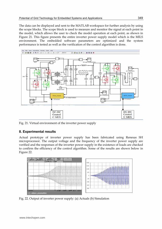
The data can be displayed and sent to the MATLAB workspace for further analysis by using the scope blocks. The scope block is used to measure and monitor the signal at each point in the model, which allows the user to check the model operation at each point, as shown in Figure 21. This figure presents the entire inverter power supply model which is the MILS environment. The embedded software parameters are optimized and the system performance is tested as well as the verification of the control algorithm is done.
Fig. 21. Virtual environment of the inverter power supply
8. Experimental results
Actual prototype of inverter power supply has been fabricated using Renesas SH microprocessor. The output voltage and the frequency of the inverter power supply are verified and the responses of the inverter power supply in the existence of loads are checked to confirm the efficiency of the control algorithm. Some of the results are shown below in Figure 22.
Fig. 22. Output of inverter power supply: (a) Actuals (b) Simulation
www.intechopen.com

Grid Computing – Technology and Applications, Widespread Coverage and New Horizons
350
One of the effective parameters of the inverter power supply is the time it can reach its
stationary value. Figure 22 describes this parameter and it is clear that the shapes of the
wave are visually identical. We can conclude that the developed models can simulate the
actual prototype in a good way within very short time comparing to the traditional method
of design. The output voltage and frequency are tested, as shown in Figure 23 as well as the
relationship between the output waves and the generated PWM signals which are generated
by the microprocessor and controlled by the embedded software.
In Figure 23, comparing the two waveforms, it can be seen that the result obtained by the
developed model is in a good agreement with the actual result in both frequency and
voltage amplitude. It is apparent that the narrow pulse is generated when the modulating
signal is at its maximum or minimum values.
(a) Actual
(b) Simulation
Fig. 23. Sin wave output of inverter power supply:
Response with linear load
The inverter power supply output distortion or the output voltage drop is considered a very
important issue in the design of the inverter power supply. There are many regulations
regarding the allowable voltage drop in the inverter power supply. For example, based on
the standard IEC686, the allowed voltage drop is no more than 5% voltage against single
www.intechopen.com
Potential of Grid Technology for Embedded Systems and Applications
351
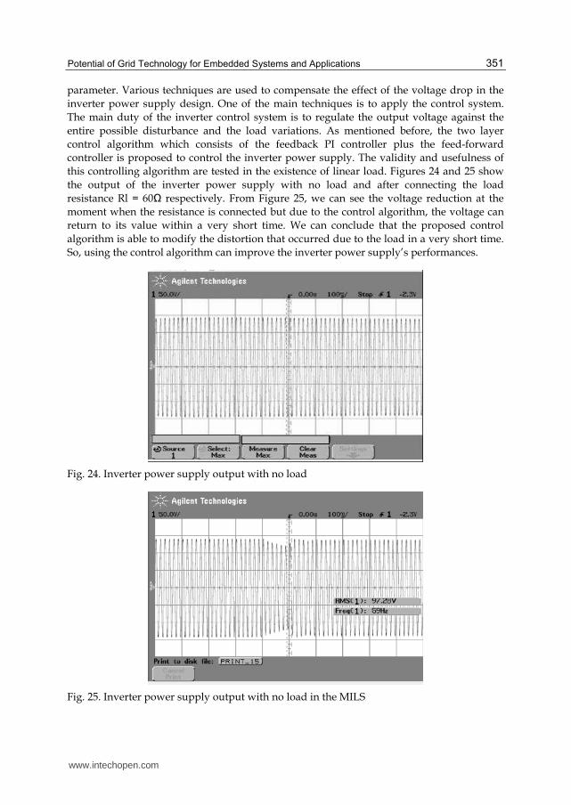
parameter. Various techniques are used to compensate the effect of the voltage drop in the
inverter power supply design. One of the main techniques is to apply the control system.
The main duty of the inverter control system is to regulate the output voltage against the
entire possible disturbance and the load variations. As mentioned before, the two layer
control algorithm which consists of the feedback PI controller plus the feed-forward
controller is proposed to control the inverter power supply. The validity and usefulness of
this controlling algorithm are tested in the existence of linear load. Figures 24 and 25 show
the output of the inverter power supply with no load and after connecting the load
resistance Rl = 60Ω respectively. From Figure 25, we can see the voltage reduction at the
moment when the resistance is connected but due to the control algorithm, the voltage can
return to its value within a very short time. We can conclude that the proposed control
algorithm is able to modify the distortion that occurred due to the load in a very short time.
So, using the control algorithm can improve the inverter power supply’s performances.
Fig. 24. Inverter power supply output with no load
Fig. 25. Inverter power supply output with no load in the MILS
www.intechopen.com

Grid Computing – Technology and Applications, Widespread Coverage and New Horizons
352
Comparing the result with no load and the result with load, it seems that the shapes of the
wave forms are almost identical except in the moment that the load resistances are
connected. The voltage decreased by about 2% of no load voltage for a very short time of
approximately 100 msec, and then it returned to its normal value. So, we can conclude that
the proposed controlling algorithm is working well, and it can maintain the disturbance
occurred due to the load connection.
9. Conclusions
This research meets the challenges of the embedded system design by applying the Model
Based Design (MBD) method in the early design stage. Furthermore, the main
contribution of this research is to prove the potential of using the MBD method in the
optimization and verification of the embedded system software development. This study
proposed the functional model of a microprocessor in the early stage of the inverter
power supply development, which allows the full simulation of the system in the virtual
environment including the electrical circuit and software implementation. Inverter power
supply was taken as a case study of the embedded system design. An entire model of the
system was developed, including the electrical circuit and the microprocessor using the
MATLAB and Simulink package. All the software parameters were optimized as well as a
newly applied controlling algorithm was evaluated using the Model In the Loop
Simulation (MILS) environment. The validity and the usefulness of the proposed model
were tested comparing with the actual prototype of the inverter power supply. The
developed model was shown to be well in agreement with the experimental results. This
method can be used to optimize the software parameters before the actual design.
Moreover, the models can be used to study and analyze the behaviors of the system which
meet the challenges of designing the digital control system. The results show that the
suggested models are promising and the models can be useful for optimizing the
performances in developing the embedded software.
10. References
Abo Eldahb, M.A. (2011). Model Based Design Environment for the Embedded System; Case study:
Inverter Power supply. Ph D Thesis, Production Science and technology Dept.,
Gunma University, Japan, Sept. 2011.
Abo Eldahb, M.A., Iino, S. Shirashi, Y.& Tatsumo, M.(2009).Model Based Design of The inverter
Power Supply, In the Proceeding of ICCAS-SICE International Joint Conference,
Fukuoka, Japan, August 17-21th, 2009.
Behboodian, A. (2006). Model Based Design. DSP Magazine, Vol.2, pp.52-56., May 2006.
Berger, A. S. (2002). Embedded Systems Design: An Introduction to Processes, Tools & Techniques.
Group West Publishers, USA.
Buyya R, Murshed M. GridSim(2002): A toolkit for the modeling and simulation of distributed
resource management and scheduling for Grid computing. Concurrency and
Computation: Practice and Experience 2002
www.intechopen.com

Potential of Grid Technology for Embedded Systems and Applications
353
Christopher, M. (2000). An Evaluation of Embedded System Behaviour” M.Sc Thesis,
Department of Electrical and Computing Engineering, University of Maryland,
2000.
Choi, S. Yong, Y. Lim W. & Young, S. (1999).A Novel Dead Time Minimization Algorithm on the
PWM Inverter, In the Proceeding of the Industrial Application Conference, IEEE,
Vol.4, pp.2188-2193, 3-7 October, 1999.
Davey, C. & Friedman, J. (2007). Software Systems Engineering with Model-Based Design. In the
Proceedings of the Fourth International Workshop on Software Engineering for
Automotive System, pp. 7, May 20-26, 2007.
Henzinger, T. & Sifakis, J. (2006). The Embedded System Design Challenge. In the Proceedings
of the 14th International Symposium on Formal Methods (FM), May 2006.
Ho, W. K. Lee T. H. & Tay.(1999).Knowledge-Based Multivariable PID Control. Technical
Notes, National University of Singapore, April, 1999.
Hongxing, W. & Tianmiao, W. (2006). Curriculum of Embedded System for Software Colleges. In
the Proceedings of the 2nd IEEE, August 2006.
Madhukar, A. & Lee, I. (2008). Challenges and Opportunities in Deeply Embedded System
Security. ACM SIGBED Journal, Vol. 5, January 2008.
Manfred, B. (2006). Challenges in Automotive Software Engineering. In the Proceedings of
ICSE’06 Conference, May 20-28th, 2006.
Mark B., Rajkumar B. & Domenico L.(2002). Grids and Grid technologies for wide-area
distributed computing: Software-Practice and Experience, Vol.32, issue 15, Pp 1437-
1466, Dec., 2002
Ming-Shan, L. (2007). Application of Embedded System in Construction Machinery. In the
Proceedings of the 8th ACIS International Conference, 30th July-1st August, 2007.
Mohan,T.M,(1995). Power Electronic Converters: Applications and Design. John Wiley &Sons
Co., Ltd, 1995.
Mosterman, P.J., (2010). Model Based Design for Embedded System. Taylor &Francis Group Co.,
Ltd., New York, 2010.
Rautio, J. (2008). Shortening the Design Cycle. Microwave Magazine, IEEE, Vol.9, No.6, pp.86-
96, Dec. 2008.
Sh-2Sh7047 Group Hardware Manual, Accessed in September 2009,
http://www.renrsas.com.
Stepner, D., & Rajac, N. & Hui, D., “Embedded Application Design Using a Real-time OS”,
In proceeding of the 36th of Design Automation Conference, New Orleans UAS,
pp. 151-156, 21-25, June 1999.
Stepner, D., & Rajan, N., & Hui, D. (1999). Embedded Application Design Using a Real-time OS.
In the proceeding of 36th Design Automation Conference, pp.151-156, New Orleans,
USA, 21-25, June 1999.
The MathWork web site, Accessed in December, 2010.http://www.mathworks.com/.
Thomas, B. (2006). Embedded Robotics: Mobile Robot Design and Application with Embedded
system. Springer- Verlag Hiedelerg Ltd. Co., Year(2006).
Turley, J. (2010). Embedded processors by the numbers. Accesses in October, 2010, Available
<http://vault.embedded.com/1999/9905/9905turley.htm>
www.intechopen.com

Grid Computing – Technology and Applications, Widespread Coverage and New Horizons
354
Woodward, V. & Mosterman, J. (2007). Challenges for Embedded Software Development. In the
Proceeding of Circuit and System, MWSCAS Conference, pp.630-633, 5-8th August,
2007.
Xue Y., Baekhy K. & Bordonau, J. ( 2004).Topologies of Single Phase Inverter for Small
Distributed Power Generators: An Overview, Transactions, IEEE, Vol.19, No.5,
September, 2004.
www.intechopen.com

Grid Computing - Technology and Applications, WidespreadCoverage and New HorizonsEdited by Dr. Soha Maad
ISBN 978-953-51-0604-3Hard cover, 354 pagesPublisher InTechPublished online 16, May, 2012Published in print edition May, 2012
InTech EuropeUniversity Campus STeP Ri Slavka Krautzeka 83/A 51000 Rijeka, Croatia Phone: +385 (51) 770 447 Fax: +385 (51) 686 166www.intechopen.com
InTech ChinaUnit 405, Office Block, Hotel Equatorial Shanghai No.65, Yan An Road (West), Shanghai, 200040, China
Phone: +86-21-62489820 Fax: +86-21-62489821
Grid research, rooted in distributed and high performance computing, started in mid-to-late 1990s. Soonafterwards, national and international research and development authorities realized the importance of theGrid and gave it a primary position on their research and development agenda. The Grid evolved from tacklingdata and compute-intensive problems, to addressing global-scale scientific projects, connecting businessesacross the supply chain, and becoming a World Wide Grid integrated in our daily routine activities. This booktells the story of great potential, continued strength, and widespread international penetration of Gridcomputing. It overviews latest advances in the field and traces the evolution of selected Grid applications. Thebook highlights the international widespread coverage and unveils the future potential of the Grid.
How to referenceIn order to correctly reference this scholarly work, feel free to copy and paste the following:
Mona Abo El-Dahb and Yoichi Shiraishi (2012). Potential of Grid Technology for Embedded Systems andApplications, Grid Computing - Technology and Applications, Widespread Coverage and New Horizons, Dr.Soha Maad (Ed.), ISBN: 978-953-51-0604-3, InTech, Available from: http://www.intechopen.com/books/grid-computing-technology-and-applications-widespread-coverage-and-new-horizons/potential-of-grid-technology-for-embedded-systems-and-applications

© 2012 The Author(s). Licensee IntechOpen. This is an open access articledistributed under the terms of the Creative Commons Attribution 3.0License, which permits unrestricted use, distribution, and reproduction inany medium, provided the original work is properly cited.