Embed Size (px)
Citation preview

2004. 03. 02 TITech A. Matsuzawa 1
Potential and limitation of RF CMOS Technologyand expectation for new passive devices
Akira Matsuzawa
Department of Physical ElectronicsTokyo Institute of Technology

2004. 03. 02 TITech A. Matsuzawa 2
Contents
• Current status of RF CMOS technology• Feature of RF CMOS technology
– Comparison with bipolar– Scaling rule– RF CMOS circuits– Architecture
• Expectation for new passive devices– Inductor, resonator, switches– Needs for reconfigurable RF circuits
• Summary

2004. 03. 02 TITech A. Matsuzawa 3
Current status of RF CMOS chip
• Current products– Bluetooth: 2.4GHz, CSR etc., major– Wireless LAN: 5GHz, Atheros etc., major– CDMA : 0.9GHz-1.9GHz, Qualcomm, becomes major– Zigbee: 2.4GHz, not yet, however must use CMOS– TAG: 2.4GHz, Hitachi etc., major
Major Cellular phone standard, GSM uses SiGe-BiCMOS technology
RF CMOS was an university research theme, however currently becomes major technologies in the wireless world.

2004. 03. 02 TITech A. Matsuzawa 4
Why CMOS?
• Low cost– Must be biggest motivation– CMOS is 30-40% lower than Bi-CMOS
• High level system integration– CMOS is one or two generations advanced– CMOS can realize a full system integration
• Stable supply and multi-foundries– Fabs for SiGe-BiCMOS are very limited.
Slow price decrease and limited product capability• Easy to use
– Universities and start-up companies can use CMOS with low usage fee, but SiGe is difficult to use such programs.

2004. 03. 02 TITech A. Matsuzawa 5
Wafer cost example
0
500
1000
1500
2000
2500
3000
3500
4000
4500
0.35
_C
0.25
_C0.
25Si
Ge_
BC0.
25_S
iGe_
BC0.
18um
_C0.
15um
_C0.
13um
_C
7M
6M
5M
4M
3M
Low costSiGe
45%45% 23%
30%
Dataquest March 2001+SiGe estimation
The wafer cost of SiGe BiCMOS is 30-40% higher than CMOS at the same generation, however almost same as one generation advanced CMOS.

2004. 03. 02 TITech A. Matsuzawa 6
RF CMOS device technology
RFCMOS
RFCMOS
Thicker MetalVaractor
High Rsub
Small lossESD High-R
LargerCap.
SmallMismatch
Conventional CMOS technologyConventional CMOS technology
Higher voltage
Hi-Q inductor
RF CMOS needs some process options,however significant cost increase can’t be accepted.

2004. 03. 02 TITech A. Matsuzawa 7
MOS vs SiGe-Bip
MOS SiGe-Bip
GmmV
IdsVIds
eff 1002
≈⎟⎠⎞
⎜⎝⎛ mV
IdsUIds
T 26≈
4x
fTpeak2
1bW
≈g
sat
Lv
∝Almost same
Fmin
2
7.0221 ⎟⎟⎠
⎞⎜⎜⎝
⎛++≈
Tff
gmGp
2
25.02
21 ⎟⎟⎠
⎞⎜⎜⎝
⎛++≈
Tff
gmGp
Lower and low Id
(larger gm)
V*fT 100VGHz 200VGHz2x

2004. 03. 02 TITech A. Matsuzawa 8
MOS vs SiGe-Bip
MOS SiGe-BipRg,Rb
Same
1/f noiseMuch better
Mismatch )()(
umLWnmToxmV ≈
Better
Cost (SiGe-BiCMOS)
Low gm or larger currentVoltage loweringGeometry dependence
High gm or smaller currentLow noise and mismatchLess geometry dependence
Low performance and low cost? High performance and high cost?
2004. 03. 02 TITech A. Matsuzawa 9
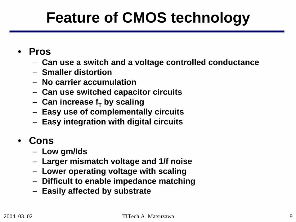
Feature of CMOS technology
• Pros– Can use a switch and a voltage controlled conductance– Smaller distortion– No carrier accumulation – Can use switched capacitor circuits– Can increase fT by scaling– Easy use of complementally circuits– Easy integration with digital circuits
• Cons– Low gm/Ids– Larger mismatch voltage and 1/f noise– Lower operating voltage with scaling– Difficult to enable impedance matching– Easily affected by substrate

2004. 03. 02 TITech A. Matsuzawa 10
Principal design for RF CMOS
• Use small size devices and compensate the accuracy and 1/f noise degradation.– Small parasitic capacitance is imperative.
• Smaller capacitance is needed to keep higher cutoff frequency under the lower gm condition
– Small size results in increase of the mismatch voltage and 1/f noise • Should be addressed by analog or digital compensation,
not by increase of device size.
• Keep the voltage swing on ahigh as possible to realize higher SNR– The noise level is higher and gm is lower than those of bipolar.
• Use digital technology rather than analog technology– Performance increase and power and area decrease are promised by
scaling. Analog is not so.

2004. 03. 02 TITech A. Matsuzawa 11
Scaling Rule: Basic principle of LSI technology
tox
L
W
ScalingDevice/Circuit parameter Scaling FactorDevice dimensions L, W, Tox 1/SDoping concentration SVoltage 1/SField 1Current 1/SGate Delay 1/SPower dissipation/device 1/S2
Scaling rule can improve almost all the performances of LSI
2≈S
Scaling also realizes higher integration and lower LSI cost.

2004. 03. 02 TITech A. Matsuzawa 12
Scaled CMOS technology
Seven latticesGate
Si
SiO2
100nm
Transistor Cu Interconnection
Current Scaled CMOS technology is very artistic.
Matsushita’s 0.13um CMOS technology

2004. 03. 02 TITech A. Matsuzawa 13
Performance trend of micro-processors
2 times/
2 years
1994 1995 1996 1997 1998 1999 2000
300MHz
200MHz
400MHz500MHz
700MHz
1GHz
100MHz
(CY)
21064
21164
2116421164 21264
21264
Pentium
R4400P6
P6 P6P6MMX2
P7
Merced
R3000 V810
R4200
SuuperSparcR3900
SH3
R4300 SH3
R4300SA110US
R4400 Pentium MMX
SH4 V830R
V832
R12000PPC604e
US-2
US-3
IBM
NEC
R14000
2001 2002SH2
V830
R10000R5000
SA110
PPC750R10000 Embedded
High-endPC
Year
Ope
ratin
g fr
eque
ncy
Performance of micro-processors has increased with device scaling.

2004. 03. 02 TITech A. Matsuzawa 14
GHz operation by CMOS
inT
Cgmfπ2
≡
Cutoff frequency of MOS becomes higher along with technology scalingand now attains over 100GHz.
1995 2000 2005
1G
10G
100G
100M
Freq
uenc
y (H
z)
200M
500M
2G
5G
20G
50GfT : Bipolar (w/o SiGe)
fT
Year
eff
satTpeak
Lvfπ2
≈
D R/C for HDDIEEE 1394
/60 (CMOS )Digital circuits
fT : CMOS
0.35um
0.25um0.18um
0.13um
fT
CellularPhone
/10 (CMOS )
CDMA
RF circuits
5GHz W-LAN

2004. 03. 02 TITech A. Matsuzawa 15
Vdd and CMOS scaling limits
0
1
2
3
4
1 2 3 4 5 6 7 8 9 10 11 12 13 14 15
アナログ(上限)
アナログ(下限)
デジタル(上限)
デジタル(下限)
テクノロジーノード
‘00 ‘05 ‘100
1
2
3
4
1 2 3 4 5 6 7 8 9 10 11 12 13 14 15
Tec
hnol
ogy
node
(0.1
um) Analog (Upper)
Analog (Lower)
Digital (Upper)
Digital (Lower)
Technology node
‘00 ‘05 ‘10
Supp
ly v
olta
ge (V
)
ITRS ‘99
Lowest analog operating voltage is 1.2V -1.8V.Thus 0.18um – 0.13um must be a scaling limit for analog.50 GHz-100 GHz is an available fT in CMOS technology.

2004. 03. 02 TITech A. Matsuzawa 16
Difficulty of low voltage analog
0.1 1 10 10050
60
70
80
90
10095.918
51.938
SNRC 1 2, C,( )
SNRC 2 2, C,( )
SNRC 3 2, C,( )
SNRC 5 2, C,( )
1000.1 C
14bit
12bit
10bit
CnkTVn =2
⎟⎟⎠
⎞⎜⎜⎝
⎛=
nkTCVSNR FS
dB8
log102
)(
SN
R (d
B)
Capacitance (pF)0.1 1 10 100
VFS=5VVFS=3V
VFS=2V
VFS=1V
N=2
Low voltage swing results in low SNR, because noise can’t be scaled.
SNR
(dB
)

2004. 03. 02 TITech A. Matsuzawa 17
Cost up issue by analog parts
0
0.1
0.2
0.3
0.4
0.5
0.6
0.7
0.8
0.9
1
0.35um 0.25um 0.18um 0.13um0
0.1
0.2
0.3
0.4
0.5
0.6
0.7
0.8
0.9
1
0.35um 0.25um 0.18um 0.13um
(0.35um : 1)
Chip area Chip cost
I/OAnalog
Digital
Wafer cost increases 1.3xfor one generation
The cost of mixed A/D LSI will increase when using deep sub-micron device, due to the increase of the cost of non-scalable analog parts.
Large analog may be unacceptable.Some analog circuits should be replaced by digital circuits

2004. 03. 02 TITech A. Matsuzawa 18
Minimum noise figure: Fmin
0.01.02.0
3.04.05.06.0
7.08.0
0.11Gate length (μm)
0.35 0.250.5
Fmin
(dB
)
T
o
gmgm
ffF
ee
2
minR
R21κ
αδκα
γ+⎟
⎠⎞
⎜⎝⎛ +⎟⎟
⎠
⎞⎜⎜⎝
⎛+≈
Imput
Output
L1
LsCpi
Rsub
M1
M2
High fT and low gate resistance.Small current in substrate.PAD and ESD structure.
Fmin has been improved , however saturated at 1dB.
Technical points

2004. 03. 02 TITech A. Matsuzawa 19
Substrate effect on NF in MOS
MOS
NFmin@5GHz,0.18um
Packaged
On chip
(Substrate loss shall be added, when packaged)
This is due to the substrate RF power loss
・Packaged:NFmin=1.6dB・On chip:NFmin=0.4dB E.Morifuji, et al., SSDM98 pp.80-81
NF in MOS is very low at on a chip measurement,But becomes very large when packaged!

2004. 03. 02 TITech A. Matsuzawa 20
Mixer
Lo Lo
LoLo
Vin
Vin
Vo Vo
No conversion gainNo isolation, Bi-directional
Lo Lo
Vo
Vin
Lo
Vo
Vin
RL
RL
Larger powerLarger distortionLarger 1/f noise
High conversion gainHigh isolation
Low powerHigh linearityNo 1/F noise
Active mixer (same as bipolar) Passive mixer (MOS only)
The passive mixer can be realized by CMOS only.High linearity, no 1/f noise effect, and low power are realized.
2004. 03. 02 TITech A. Matsuzawa 21
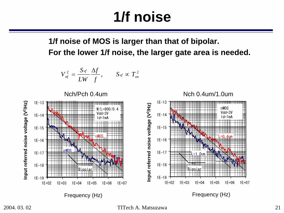
1/f noise
1E-19
1E-18
1E-17
1E-16
1E-15
1E-14
1E-13
1E+02 1E+03 1E+04 1E+05 1E+06 1E+07
L=0.4um
L=1.0um
Bipolar
nMOSVdd=3VId=1mA
1E-19
1E-18
1E-17
1E-16
1E-15
1E-14
1E-13
1E+02 1E+03 1E+04 1E+05 1E+06 1E+07
nMOS
pMOS
W/L=800/0.4Vdd=3VId=1mA
Bipolar
2
Inpu
t ref
erre
d no
ise
volta
ge (V
2 /Hz)
Frequency (Hz) Frequency (Hz)
Inpu
t ref
erre
d no
ise
volta
ge (V
2 /Hz)
Nch/Pch 0.4um Nch 0.4um/1.0um
1/f noise of MOS is larger than that of bipolar.
22 , oxvfvf
nf TSff
LWSV ∝
Δ=
For the lower 1/f noise, the larger gate area is needed.

2004. 03. 02 TITech A. Matsuzawa 22
L
C
L
CVc
Vb
Vo VoL
C
L
C
Vb
Vc
Vo Vo
L
C
L
C
Vb
Vc
Vo Vo
Cx
LxCsHi-Z at 2fo
(a) (b)(c)
CMOS oscillator circuits
Basic Low power (gm is higher) Low noise by filtering
E. Hegazi, ISSCC 2001

2004. 03. 02 TITech A. Matsuzawa 23
-150.0
-140.0
-130.0
-120.0
-110.0
-100.0
-90.0
1994 1995 1996 1997 1998 1999 2000 2001 2002
SSB
Pha
se N
oise
[d
Bc/
Hz]
(@1
GH
z,10
mW
,600
kHz)
◆CMOS
■Si-bipolar/BiCMOS
▲SiGe-BiCMOS
Year
Oscillator phase noise progressPhase noise in CMOS oscillator becomes lower than that of bipolar.
⎟⎟⎠
⎞⎜⎜⎝
⎛⋅⋅∝
m
o
o
mff
QVfL 22
11)(
The larger voltage swing in MOS Oscillator realizes lower oscillation phase noise.
(High Q inductance is also very effective to reduce phase noise)
2004. 03. 02 TITech A. Matsuzawa 24
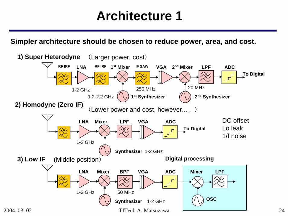
Architecture 1
RF IRF RF IRFLNA 1st Mixer 2nd MixerVGA LPF ADCTo Digital
IF SAW
1st Synthesizer 2nd Synthesizer
1) Super Heterodyne
2) Homodyne (Zero IF)
LNA Mixer LPF ADCTo Digital
VGA
Synthesizer
3) Low IF
LNA Mixer BPF ADCVGA
Synthesizer
1-2 GHz1.2-2.2 GHz
250 MHz 20 MHz
1-2 GHz
1-2 GHz
LPFMixer
1-2 GHz 50 MHzOSC1-2 GHz
Digital processing
(Larger power, cost)
(Lower power and cost, however... , )
DC offsetLo leak1/f noise
(Middle position)
Simpler architecture should be chosen to reduce power, area, and cost.

2004. 03. 02 TITech A. Matsuzawa 25
Architecture 2
4) Low IF with ΣΔADC
LNA Mixer BPF Quantizer
Synthesizer
LPFMixer
1-2 GHz 50 MHzOSC
1-2 GHz
Digital processingΣΔADC
5) Digital architecture
LNA LPF Quantizer
Synthesizer
LPFMixer
1-2 GHzOSC
1-2 GHz
Digital processingΣΔADCSampleddata LPF
Analog circuits have been replaced by digital circuits.Small analog and big digital is a technology direction.
K. Muhammad (TI), et al., ISSCC2004, pp.268
Bluetooth receiver0.13um CMOS1.5V

2004. 03. 02 TITech A. Matsuzawa 26
Technology edge RF CMOS LSI
M. Zargari (Atheros), et al., ISSCC 2004, pp.96 K. Muhammad (TI), et al., ISSCC2004, pp.268
Discrete-time Bluetooth0.13um, 1.5V, 2.4GHz
Wireless LAN, 802.11 a/b/g0.25um, 2.5V, 23mm2, 5GHz
Many RF CMOS LSIs have been developed for many standards

2004. 03. 02 TITech A. Matsuzawa 27
Advantage of SiGe Bi-CMOS
Alcatel1) OkiProcess
Chip size゙
Id
Rx_Sens.
Tx_Power
Rx
Tx
Broadcom Conexant MitsubishiCMOS0.25um
40.1mm2
50mA
-80dBm
+2dBm
70mA
CMOS0.35um
18.0mm2
47mA
-77dBm
+2.5dBm
66mA
CMOS0.35um
46mA
-80dBm
+5dBm
47mA
SiGe-BiCMOS0.5um
12mA
-78dBm
+2dBm
16.4mA
Si-BiCMOS0.5um
34.4mA
44.0mA
-80dBm
0dBm
17.0mm2
Vdd 2.7-3.3V1.8-3.6V3V(?)2.7-3.3V2.5V
SiGe Bip has a great advantage in power consumption

2004. 03. 02 TITech A. Matsuzawa 28
Potential and limitation of RF CMOS
• Potential– RF CMOS are going to be a major in the wireless products.– SiGe Bi-CMOS technology will be used for only extremely low
noise and low power RF products.– 60GHz or 100GHz CMOS circuits has already developed.
• Limitation– For low noise and low power characteristics in RF circuit, SiGe
bipolar technology must be better than CMOS. – High power PA will not be integrated on scaled CMOS chip, due to
low efficiency and needs low voltage operation.– Use of further advanced technology beyond 90nm would be limited.
This is because low analog operating voltage of less than 0.9V and chip and development cost increase.

2004. 03. 02 TITech A. Matsuzawa 29
Expectation for new passive devices
• However, passives are still important– High Q inductance
• VCO: reduce power and phase noise• LNA: reduce power and noise figure
– Tunable inductor• Multi frequency, yet single inductance.• Reconfigurable RF circuits
– RF band pass filter – RF switches
• TX/RX• Select frequency bands to address multi-standards• Reconfigurable RF circuits
– On chip solid reference Oscillator
This would sound inconsistent with RF CMOS technology
RF CMOS technology is going to reducing analog and passive components.

2004. 03. 02 TITech A. Matsuzawa 30
Inductor
2
1Q
S ∝φ
RF-CMOS LSI
Inductor
QI 1∝
Noise:
Current
L
C
L
CVc
Vb
Vo Vo
Q of inductor determines almost all the performance of RF oscillator. Q is conventionally less than 10.
RF-VCO

2004. 03. 02 TITech A. Matsuzawa 31
RF application of flip chip technology
High performance RF circuit has been realized by using the flip chip technology.
W.P.Donnay, et al., ISSCC 2000, WA 19.1
Qmax=63 @9.2GHz

2004. 03. 02 TITech A. Matsuzawa 32
Variable Inductor
50%
h=10μm
x
Conductor plate
450μm
4μm
20μm
Sliding
2.4GHz to 5.1GHz
Sliding plate can vary inductance by 50%.Wide tunable range VCO (2.4GHz to 5.1GHz) has been realized.
TITech. Masu Lab.

2004. 03. 02 TITech A. Matsuzawa 33
RF MEMS switch
J. DeNatale, ISSCC 2004, pp. 310
Mechanical low-loss integrated switch enables;
Select or change inductance and capacitanceSelect signals and circuits;As a result, enables reconfigurable RF circuits

2004. 03. 02 TITech A. Matsuzawa 34
Micromechanical-Disc Reference Oscillator
Yu-Wei Lin, et al., ISSCC 2004, pp. 322
Fo=61MHzQ=48,000-145dBc/Hz far-end-115dBc/Hz @ 1KHz
MEMS technology will realize an on-chip solid reference oscillator

2004. 03. 02 TITech A. Matsuzawa 35
Multi-standard issue
IMT-2000RF
GSMRF
BluetoothRF
GPSRF
GPSBB
BluetothBB
GSMBB
IMT-2000BB
MCU
Power
ReconfigurableRF DSP
Unification
Yrjo Neuvo, ISSCC 2004, pp.32
Unified wireless system
Multi-standards and multi chipsFuture cellular phone needs 11 wireless standard!!
Reconfigurable RF circuit is strongly needed for solving multi-standard issue.
Current
Future

2004. 03. 02 TITech A. Matsuzawa 36
Summary
• RF-CMOS technology– Becomes major
• Performance increase and full system integration due to scaling• Development of suitable circuits and architecture• Small analog and large digital is a right way• Low cost and huge supply capacity
– However, some issues• For low power and now noise, SiGe Bi-CMOS is better• Limited use of further scaled CMOS beyond 90nm
• Expectation of new passive device– Great demand for reconfigurable RF circuits:
• Switches for the reconfigurability• On chip RF filter and Oscillator• High quality and tunable inductance


![Cmos Rf Cituits Sic] Variability And Reliability Resilient](https://img.dokumen.tips/doc/110x75/61eff30f1f58b06c3f317164/cmos-rf-cituits-sic-variability-and-reliability-resilient-.jpg)