Embed Size (px)
Citation preview

PMP-10393 600 mV 120/200A 5-6 phases off 12Vin Test Report (TPS53661 / CSD95372B) Texas Instruments
Josh Mandelcorn page 1 of 14 Dec. 29, 2014 & Jan. 7, 2015
Table of Contents: Why separate report for 600mV output? this page Summary / comments on dynamic load testing this page Step load response / Load dump response page 2
Details of step load & load dump pages 3-4 5 phase thermal image 600mV 200A model t12 page 5 Also currents per phase data at bottom of page 5 phase thermal image 600mV 200A model t11 page 6 Also currents per phase data at bottom of page 5 phase thermal image 1.0V 200A model t11 page 7 Efficiency vs. load model t11 / GUI image pages 8-9 3 phase experiment with CSD95372B / CSD95373B / CSD95372B at 120 A in all to show thermal sharing when in fixed frequency & fixed pulse width modes pages 10-14
Why separate report for 600mV output:
PMP9738 has same physical design and was tested at 1.0 Vout. However, going down to 600mV with 12Vin changes the control mode of the TPS53661 from a quasi fixed frequency control with active current sharing to a fixed on time control per phase with no active current sharing. This is because of minimum pulse width of about 260 nsec per phase for the 300 kHz setting. The customer asked, “What will happen without active current sharing when power stages with normal variations in Rdson - on resistance are used?”
Also, actual switching frequency gets reduced as Vout is reduced, and ripple / dynamic response can be affected. This report first shows dynamic response & ripple for the 600mV setting. Then thermal images for two models with 5 phases each and 600mV at 200 A are shown, followed by 1.0 Vout at 200 A for comparison; and then detailed efficiency / loss data on one of the models at 600 mV out.
Finally, an experiment with (see pages 10-14) “worst case” FET on resistance variation is shown. Here, 3 phases are used and the middle phase power stage is replaced with higher on resistance / lower current rated CSD95373B. Load is set at 120 A or 40 A per phase off the 600mV output, and Vin is varied from 7 V when mode is still fixed frequency up 12V. Between 8 and 9 Vin, mode transitions to fixed pulse width and frequency starts to drop from 318 kHz reaching 226 kHz at 12 Vin. Thermal images show that heat sharing is actually improved by going to the fixed pulse width mode. Also, the combined lower frequency and improved thermal sharing create an increased efficiency with increased Vin, which is unusual for buck converters. Summary / comments on dynamic load testing: Tested on Model t11: Loop compensation values: C46=10pF; C47=1.5nF; R68=19.1k Comments: Waveforms shown with a static load of 106 A off the output. However, same tests were also done with no static load, and very similar undershoots & overshoots seen. This is because of the Forced Continuous conduction Mode (FCCM) operation. Step load was 70 A in about 8 usec and load dump was 85 A in 5 usec. Hence, load dump overshoot of 42 mV is higher than step load undershoot of 30 mV. The on board dynamic load allows speeds of step load and load dump to be adjusted independently based on actual needs of the application. The 106A static load is an external load bank, the dynamic load is on the board. See page 3 of the schematic.

PMP-10393 600 mV 120/200A 5-6 phases off 12Vin Test Report (TPS53661 / CSD95372B) Texas Instruments
Josh Mandelcorn page 2 of 14 Dec. 29, 2014 & Jan. 7, 2015
600 mV 300kHz settings: actual frequency at 600 mV off 12.0 Vin about 200 kHz Vout measured at C19: All 6 phases on Step load response from 106 A to 176 A (70 A step) in 8 usec: ~30 mV
q Load dump response from 191 A to 106 A (85 A step) in 5 usec: ~42 mV
Q

PMP-10393 600 mV 120/200A 5-6 phases off 12Vin Test Report (TPS53661 / CSD95372B) Texas Instruments
Josh Mandelcorn page 3 of 14 Dec. 29, 2014 & Jan. 7, 2015
Waveforms across resistors in dynamic load bank used to calculate step load current and speed: There are two resistor paths from Vout; R1 and R2 each 2mOhm and tied to Vout. Hence, the total load step is the sum of both. Here scope ground on Vout side of resistor. First R1 2mOhm: 70 mV in 8 usec or 35 A in 8 usec
And now R2(also 2mOhm): also 70 mV in 8 usec or 35 A in 8 usec
Load strings are in parallel driven by same FET Q1: Hence, combined: 70 A in 8 usec

PMP-10393 600 mV 120/200A 5-6 phases off 12Vin Test Report (TPS53661 / CSD95372B) Texas Instruments
Josh Mandelcorn page 4 of 14 Dec. 29, 2014 & Jan. 7, 2015
Waveforms across resistors in dynamic load bank used to calculate load dump current and speed: There are two resistor paths from Vout; R1 and R2 each 2mOhm and tied to Vout. Hence, the total load dump is the sum of both. Here scope ground on Vout side of resistor. First R1 2mOhm: 84 mV in 5 usec or 42 A in 5 usec
And now R2(also 2mOhm): 86 mV in 5 usec or 43 A in 5 usec
Load strings are in parallel driven by same FET Q1: Hence, combined: 85 A in 5 usec

PMP-10393 600 mV 120/200A 5-6 phases off 12Vin Test Report (TPS53661 / CSD95372B) Texas Instruments
Josh Mandelcorn page 5 of 14 Dec. 29, 2014 & Jan. 7, 2015
Model t12 thermals: PMP9738 adjusted to 5 phases 600mV 12Vin 220kHz actual 25.0 W on PCB ~300 LFM fan blowing in from U100 side Ambient 21-23 degrees Celsius Left to right: U100 thru U500 temperatures in deg. C: 56.7, 60.5, 62.2, 61.2, 56.7 traces / snubbers slightly hotter with hotspot near U300 at 62.6 degrees C Inductor tops Left to Right (L100 thru L500) in degrees C: 41, 44, 45, 44, 41
Q Current senses from the CSD95372Bs: Ref in for all at 1.700 V Iout (pin 1) for each going from left to right in Volts: 1.886; 1.883, 1.887, 1.891, 1.889 Currents in each based upon 5mV/A sense: 37.2 A; 36.6 A, 37.4 A; 38.2 A, 37.8 A Here, overall variation 1.6A overall variation or 187.2A in all per senses.

PMP-10393 600 mV 120/200A 5-6 phases off 12Vin Test Report (TPS53661 / CSD95372B) Texas Instruments
Josh Mandelcorn page 6 of 14 Dec. 29, 2014 & Jan. 7, 2015
Model t11 thermals: (voltage sense here further away from power train and Voltage at same sense points at 200 A load 12 mV higher at 611.4 mV vs. 599.5 mV on model t12 ) PMP9738 adjusted to 5 phases 600mV 12Vin 225kHz actual 25.8 W on PCB ~300 LFM fan blowing in from U100 side Ambient 21-23 degrees Celsius: (60 deg. C on GUI) Left to right: U100 thru U500 temperatures in deg. C: 59.6, 59.7, 63.2, 59.3, 57.0 traces / snubbers slightly hotter with hotspot near U300 at 65.1 degrees C Inductor tops Left to Right (L100 thru L500) in degrees C: 42, 44, 44, 43, 41 Model t11 thermals at 200 A:
11.9992 Vin, 12.371 Ain, 611.4mVout 200.6A out 25.79 W loss Current senses from the CSD95372Bs: Ref in for all at 1.699 V Iout (pin 1) for each going from left to right in Volts: 1.908; 1.881; 1.895; 1.881; 1.893 Currents in each based upon 5mV/A sense: 41.8A, 36.4A, 39.2A, 36.4A, 38.8A Here, overall variation 5.4A overall variation or 192.6A in all per senses.

PMP-10393 600 mV 120/200A 5-6 phases off 12Vin Test Report (TPS53661 / CSD95372B) Texas Instruments
Josh Mandelcorn page 7 of 14 Dec. 29, 2014 & Jan. 7, 2015
Model t11 at 1.0Vout 200A off 12 Vin 5 phases: PMP9738 adjusted to 5 phases 1.0V 12Vin318kHz actual 29.5 W on PCB ~300 LFM fan blowing in from U100 side LtoR ambient 21-23 deg. C U100 thru U500 power stages (left to right) max in degrees Celsius: 62, 68, 70, 68, 61 Inductors Left to Right: (L100 thru L500 tops) in degrees Celsius: 43, 47, 47, 46, 44 IR777 at 70 max, 318kHz
Q 11.999Vin 1.0155Vout, 19.437Ain 200.6Aout or 87.3% eff. Or 29.515W loss on board:

PMP-10393 600 mV 120/200A 5-6 phases off 12Vin Test Report (TPS53661 / CSD95372B) Texas Instruments
Josh Mandelcorn page 8 of 14 Dec. 29, 2014 & Jan. 7, 2015
Model t12: Model used for automatic efficiency run: Data is on next page Model first stabilized at 200 A load off 12 Vin with 300 LFM fan for 20+ minutes. Then load stepped down from 200 A to zero A in 40 steps of 5 A each with 90 seconds between each step Switching frequencies at various loads: 200 A – 220 kHz; 180 A - 216 kHz; 80 A – 199.5 kHz; 35 A – 192.5 kHz At 200 A load: Going to 6 stages saves about 3.1W. Going to 4 stages at 200A increases losses by about 6.2W. Marginal efficiency near 200 A is just over 71%. GUI at full 200 A load / 5 phases:
Q

PMP-10393 600 mV 120/200A 5-6 phases off 12Vin Test Report (TPS53661 / CSD95372B) Texas Instruments
Josh Mandelcorn page 9 of 14 Dec. 29, 2014 & Jan. 7, 2015
Efficiency data on Model t12: Vin in Volts Iin Amperes Vout Iout Efficiency % Losses in W
11.999 12.070 0.5995 200.04 82.80 24.90 11.999 11.720 0.5995 195.03 83.14 23.71 11.999 11.373 0.5995 190.02 83.48 22.54 11.999 11.028 0.5995 185.01 83.82 21.41 11.999 10.686 0.5995 180.00 84.16 20.31 11.999 10.349 0.5995 174.99 84.49 19.26 11.999 10.016 0.5995 169.97 84.80 18.27 11.999 9.685 0.5996 164.96 85.11 17.30 11.999 9.357 0.5996 159.95 85.41 16.38 11.999 9.032 0.5996 154.93 85.71 15.48 11.999 8.709 0.5996 149.93 86.02 14.61 11.999 8.389 0.5996 144.92 86.32 13.77 11.999 8.073 0.5996 139.91 86.60 12.98 11.999 7.759 0.5996 134.91 86.88 12.21 11.999 7.447 0.5996 129.90 87.16 11.47 11.999 7.138 0.5996 124.90 87.43 10.76 11.999 6.832 0.5996 119.90 87.69 10.09 11.999 6.528 0.5996 114.90 87.95 9.44 11.999 6.227 0.5996 109.90 88.19 8.82 11.999 5.929 0.5996 104.91 88.42 8.24 11.999 5.636 0.5996 99.97 88.65 7.68
11.999 5.627 0.5996 99.83 88.65 7.66 11.999 5.334 0.5996 94.86 88.87 7.12 11.999 5.043 0.5996 89.89 89.07 6.62 11.999 4.754 0.5996 84.90 89.25 6.13 11.999 4.467 0.5997 79.91 89.39 5.68 11.999 4.183 0.5996 74.92 89.51 5.26 11.999 3.900 0.5997 69.93 89.60 4.87 11.999 3.620 0.5997 64.93 89.63 4.50 11.999 3.342 0.5997 59.93 89.62 4.16 11.999 3.066 0.5997 54.93 89.54 3.85 11.999 2.792 0.5997 49.93 89.37 3.56 11.999 2.527 0.5997 44.93 88.87 3.37 11.999 2.261 0.5997 39.93 88.28 3.18 11.999 1.985 0.5997 34.93 87.96 2.87 11.999 1.704 0.5997 29.93 87.79 2.50 11.999 1.431 0.5997 24.93 87.09 2.22 11.999 1.166 0.5998 19.94 85.48 2.03 11.999 0.908 0.5998 14.94 82.28 1.93 11.999 0.652 0.5998 9.94 76.17 1.86 11.999 0.399 0.5998 4.95 61.98 1.82 11.999 0.149 0.5998 0.00 0.00 1.79
Q

PMP-10393 600 mV 120/200A 5-6 phases off 12Vin Test Report (TPS53661 / CSD95372B) Texas Instruments
Josh Mandelcorn page 10 of 14 Dec. 29, 2014 & Jan. 7, 2015
Question arose about using this design for cases when Vin / Vout is greater than about 13 to 1 and minimum pulse width of about 260 nsec effectively removes the active current sharing with each phase being driven with a fixed on time in turn. What will happen if the FETs have a “worst case” imbalance and there is no active current sharing?
I came up with an experiment with 3 phases 120A load and middle U20 FET being CSD95373B with 25% more Rdson, but same 5mV/A sense: The two outer FETs U100 & U300 remain the same CSD95372B’s that have been in the design.
Model was run with fan on the U100 side and in each case until thermal stabilization. Then the Vin, Iin, Vout, Iout and phase frequency was recorded. Then the Iout from each phase and Vref were recorded, and the currents for each phase calculated based upon 5mV per A gain of this current sense. Then the thermal image of the board was taken with Flir EX320 thermal camera (e = 0.94) and the max temperatures of the 3 FETs recorded. At 12Vin data was taken for both 1.0 Vout with fixed frequency operation and active current sharing, and at 600 mV with fixed pulse width and no active current sharing occurs. Then at 600mV (all runs with 120 A load) the input voltage was reduced in steps to 7 Vin, with the mode transitioning back to fixed frequency as Vin was reduced below 9 Vin. Summary of data:
Mode Sw Freq Vin (V) Iin (A) Vout(V) Iout(A) eff %
losses W
fix freq 321 kHz 12.071 11.640 1.013 120.0 86.5 18.95
fix pulse 226 kHz 12.067 7.445 0.611 120.0 81.6 16.52
fix pulse 260 kHz 10.53 8.543 0.611 120.0 81.5 16.64
fix pulse 305 kHz 9.027 10.000 0.611 120.0 81.2 16.95
fix freq 318 kHz 8.009 11.340 0.611 120.0 80.7 17.50
fix freq 318 kHz 6.97 13.045 0.611 120.0 80.6 17.60
U100 U200 U300 sum U100 U200 U300
Vin (V) Vout(V)
sensed current-
A
sensed current-
A
sensed current-
A
sensed current-
A max
deg C
max deg
C max
deg C 12.071 1.013 39.1 37.5 39.3 115.9 57.5 69.9 59.4 12.067 0.611 42.6 30.6 43.2 116.4 56.0 56.9 58.1
10.53 0.611 42.6 30.8 43.2 116.6 56.5 57.6 58.8 9.027 0.611 42.2 31.2 43.2 116.6 56.6 58.3 59.5 8.009 0.611 39.2 38.0 39.2 116.4 56.0 68.8 57.8
6.97 0.611 39.2 38.2 39.2 116.6 55.7 68.6 57.7 See actual thermal images below spread over 3 pages. Conclusion: Allowing reduced frequency and fixed pulse widths can reduce temperature of hottest FET by as much as 10 degrees Celsius. This supported by both the Flir EX320 thermal camera and the internal temperature monitoring in the CSD9537xBs and TPS53661. (See next page for GUI.) In all previous high current 12V to low Vout / high current designs it has been assumed that increasing Vin makes efficiency worse. Here with mode transition and reduced frequency, efficiency is actually 1% better at 12 Vin than at 7 Vin.

PMP-10393 600 mV 120/200A 5-6 phases off 12Vin Test Report (TPS53661 / CSD95372B) Texas Instruments
Josh Mandelcorn page 11 of 14 Dec. 29, 2014 & Jan. 7, 2015
GUI of temperature of hottest FET vs. Vin with 611mV 120A out: In top image Vin is slowly increased from 7V to 12V: 8.7 degrees C reduction seen with most of change when Vin increased from 8V to 9V changing from constant frequency with active current sharing to constant on time per phase with no active current sharing:
In this image Vin is slowly reduced from 12V to 7V:
Q

PMP-10393 600 mV 120/200A 5-6 phases off 12Vin Test Report (TPS53661 / CSD95372B) Texas Instruments
Josh Mandelcorn page 12 of 14 Dec. 29, 2014 & Jan. 7, 2015
Thermal Images for 3 phase experiment with U200 CSD95373B:12Vin 1.013V 120A out
Q 12Vin 611mV 120A out
PMP-10393 600 mV 120/200A 5-6 phases off 12Vin Test Report (TPS53661 / CSD95372B) Texas Instruments
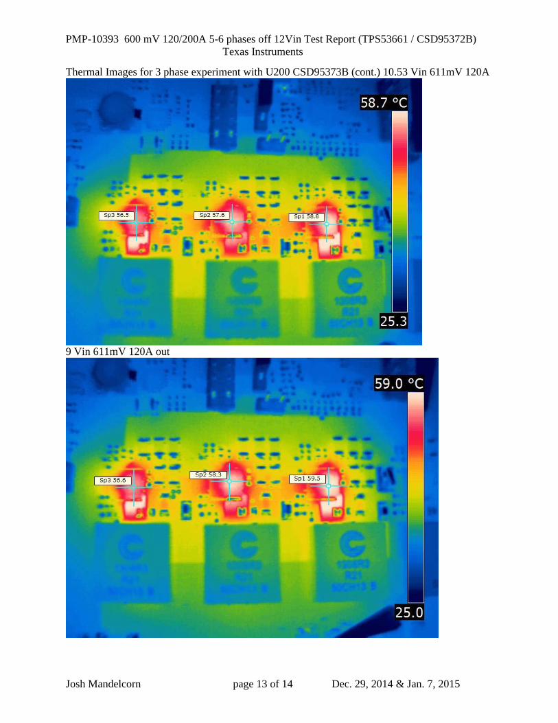
Josh Mandelcorn page 13 of 14 Dec. 29, 2014 & Jan. 7, 2015
Thermal Images for 3 phase experiment with U200 CSD95373B (cont.) 10.53 Vin 611mV 120A
9 Vin 611mV 120A out

PMP-10393 600 mV 120/200A 5-6 phases off 12Vin Test Report (TPS53661 / CSD95372B) Texas Instruments
Josh Mandelcorn page 14 of 14 Dec. 29, 2014 & Jan. 7, 2015
Thermal Images for 3 phase experiment with U200 CSD95373B (cont.) 8 Vin 611mV 120A out
7 Vin 611mV 120A out

IMPORTANT NOTICE FOR TI REFERENCE DESIGNS
Texas Instruments Incorporated ("TI") reference designs are solely intended to assist designers (“Buyers”) who are developing systems thatincorporate TI semiconductor products (also referred to herein as “components”). Buyer understands and agrees that Buyer remainsresponsible for using its independent analysis, evaluation and judgment in designing Buyer’s systems and products.TI reference designs have been created using standard laboratory conditions and engineering practices. TI has not conducted anytesting other than that specifically described in the published documentation for a particular reference design. TI may makecorrections, enhancements, improvements and other changes to its reference designs.Buyers are authorized to use TI reference designs with the TI component(s) identified in each particular reference design and to modify thereference design in the development of their end products. HOWEVER, NO OTHER LICENSE, EXPRESS OR IMPLIED, BY ESTOPPELOR OTHERWISE TO ANY OTHER TI INTELLECTUAL PROPERTY RIGHT, AND NO LICENSE TO ANY THIRD PARTY TECHNOLOGYOR INTELLECTUAL PROPERTY RIGHT, IS GRANTED HEREIN, including but not limited to any patent right, copyright, mask work right,or other intellectual property right relating to any combination, machine, or process in which TI components or services are used.Information published by TI regarding third-party products or services does not constitute a license to use such products or services, or awarranty or endorsement thereof. Use of such information may require a license from a third party under the patents or other intellectualproperty of the third party, or a license from TI under the patents or other intellectual property of TI.TI REFERENCE DESIGNS ARE PROVIDED "AS IS". TI MAKES NO WARRANTIES OR REPRESENTATIONS WITH REGARD TO THEREFERENCE DESIGNS OR USE OF THE REFERENCE DESIGNS, EXPRESS, IMPLIED OR STATUTORY, INCLUDING ACCURACY ORCOMPLETENESS. TI DISCLAIMS ANY WARRANTY OF TITLE AND ANY IMPLIED WARRANTIES OF MERCHANTABILITY, FITNESSFOR A PARTICULAR PURPOSE, QUIET ENJOYMENT, QUIET POSSESSION, AND NON-INFRINGEMENT OF ANY THIRD PARTYINTELLECTUAL PROPERTY RIGHTS WITH REGARD TO TI REFERENCE DESIGNS OR USE THEREOF. TI SHALL NOT BE LIABLEFOR AND SHALL NOT DEFEND OR INDEMNIFY BUYERS AGAINST ANY THIRD PARTY INFRINGEMENT CLAIM THAT RELATES TOOR IS BASED ON A COMBINATION OF COMPONENTS PROVIDED IN A TI REFERENCE DESIGN. IN NO EVENT SHALL TI BELIABLE FOR ANY ACTUAL, SPECIAL, INCIDENTAL, CONSEQUENTIAL OR INDIRECT DAMAGES, HOWEVER CAUSED, ON ANYTHEORY OF LIABILITY AND WHETHER OR NOT TI HAS BEEN ADVISED OF THE POSSIBILITY OF SUCH DAMAGES, ARISING INANY WAY OUT OF TI REFERENCE DESIGNS OR BUYER’S USE OF TI REFERENCE DESIGNS.TI reserves the right to make corrections, enhancements, improvements and other changes to its semiconductor products and services perJESD46, latest issue, and to discontinue any product or service per JESD48, latest issue. Buyers should obtain the latest relevantinformation before placing orders and should verify that such information is current and complete. All semiconductor products are soldsubject to TI’s terms and conditions of sale supplied at the time of order acknowledgment.TI warrants performance of its components to the specifications applicable at the time of sale, in accordance with the warranty in TI’s termsand conditions of sale of semiconductor products. Testing and other quality control techniques for TI components are used to the extent TIdeems necessary to support this warranty. Except where mandated by applicable law, testing of all parameters of each component is notnecessarily performed.TI assumes no liability for applications assistance or the design of Buyers’ products. Buyers are responsible for their products andapplications using TI components. To minimize the risks associated with Buyers’ products and applications, Buyers should provideadequate design and operating safeguards.Reproduction of significant portions of TI information in TI data books, data sheets or reference designs is permissible only if reproduction iswithout alteration and is accompanied by all associated warranties, conditions, limitations, and notices. TI is not responsible or liable forsuch altered documentation. Information of third parties may be subject to additional restrictions.Buyer acknowledges and agrees that it is solely responsible for compliance with all legal, regulatory and safety-related requirementsconcerning its products, and any use of TI components in its applications, notwithstanding any applications-related information or supportthat may be provided by TI. Buyer represents and agrees that it has all the necessary expertise to create and implement safeguards thatanticipate dangerous failures, monitor failures and their consequences, lessen the likelihood of dangerous failures and take appropriateremedial actions. Buyer will fully indemnify TI and its representatives against any damages arising out of the use of any TI components inBuyer’s safety-critical applications.In some cases, TI components may be promoted specifically to facilitate safety-related applications. With such components, TI’s goal is tohelp enable customers to design and create their own end-product solutions that meet applicable functional safety standards andrequirements. Nonetheless, such components are subject to these terms.No TI components are authorized for use in FDA Class III (or similar life-critical medical equipment) unless authorized officers of the partieshave executed an agreement specifically governing such use.Only those TI components that TI has specifically designated as military grade or “enhanced plastic” are designed and intended for use inmilitary/aerospace applications or environments. Buyer acknowledges and agrees that any military or aerospace use of TI components thathave not been so designated is solely at Buyer's risk, and Buyer is solely responsible for compliance with all legal and regulatoryrequirements in connection with such use.TI has specifically designated certain components as meeting ISO/TS16949 requirements, mainly for automotive use. In any case of use ofnon-designated products, TI will not be responsible for any failure to meet ISO/TS16949.IMPORTANT NOTICE
Mailing Address: Texas Instruments, Post Office Box 655303, Dallas, Texas 75265Copyright © 2015, Texas Instruments Incorporated