Embed Size (px)
Citation preview

Plasma and Ion Assistance in Physical Vapor Deposition: A Historical Perspective
André Anders
Lawrence Berkeley National Laboratory, University of California, 1 Cyclotron Road, Berkeley, California 94720
[email protected] Abstract
Deposition of films using plasma or plasma-assist can be traced back surprisingly far, namely to the 18th century for arcs and to the 19th century for sputtering. However, only since the 1960s the coatings community considered other processes than evaporation for large scale commercial use. Ion Plating was perhaps the first important process, introducing vapor ionization and substrate bias to generate a beam of ions arriving on the surface of the growing film. Rather independently, cathodic arc deposition was established as an energetic condensation process, first in the former Soviet Union in the 1970s, and in the 1980s in the Western Hemisphere.
About a dozen various ion-based coating technologies evolved in the last decades, all characterized by specific plasma or ion generation processes. Gridded and gridless ion sources were taken from space propulsion and applied to thin film deposition. Modeling and simulation have helped to make plasma and ions effects to be reasonably well understood. Yet —due to the complex, often non-linear and non-equilibrium nature of plasma and surface interactions— there is still a place for the experienced ion and plasma “sourcerer.”
I. Introduction
The 50th Anniversary of the Society of Vacuum Coaters is an excellent opportunity to review one important cornerstone of our technology, the fabrication of the films and coatings with plasma and ion beam assistance. While the generation and initial applications of plasmas and films occurred many years before the Society’s founding, crucial developments fall well within the last fifty years.
One can generally distinguish between the use of plasma to generate condensable material, such as the plasma used in sputtering magnetrons, and the plasma and beams directly involved in the nucleation and growth of films. The emphasis is here on the latter although we have to consider the different plasma generation schemes, too, because they often define the name and understanding of the technology.
Plasma and ion beam assistance are primarily applied to achieve desirable properties of the film or coating. They are also used to enable executing a process in a desirable way, for example to operate with a relatively low substrate bulk temperature. In a limited sense, thermal energy is replaced by the energy of the particles impinging on the surface. Yet, thermal energy on the one hand and plasma and ion particle energies on the other hand are not equivalent. Plasma and ion beam processing are generally far from thermodynamic equilibrium, and therefore the materials obtained are often metastable, highly stressed, hard or even superhard, etc.
This brief review is organized by a few key technologies. Often other, perhaps equivalent terminology may exist. Of course, given the limit of a few pages, the following review is necessarily incomplete. Only selected highlights can be mentioned in
the hope to give a flavor for the enormous progress that has been archived scientifically and practically over the last 50 years.
II. Some early developments: Setting the stage
Plasma has been generated by mankind as soon as stored electrical energy could be provided. By the middle of the 18th century, Leyden jars (capacitors) were charged through increasingly sophisticated machines making use of frictional electrostatic charge separation [1]. With the beginning of the 19th century, a new energy source became available: Voltaic piles, the early forms of batteries of electrochemical cells. Within a few years after their invention they were scaled to 2000 elements and greater, providing plenty of (dangerous and expensive) energy. These developments are well documented by professional and amateur historians [2-9].
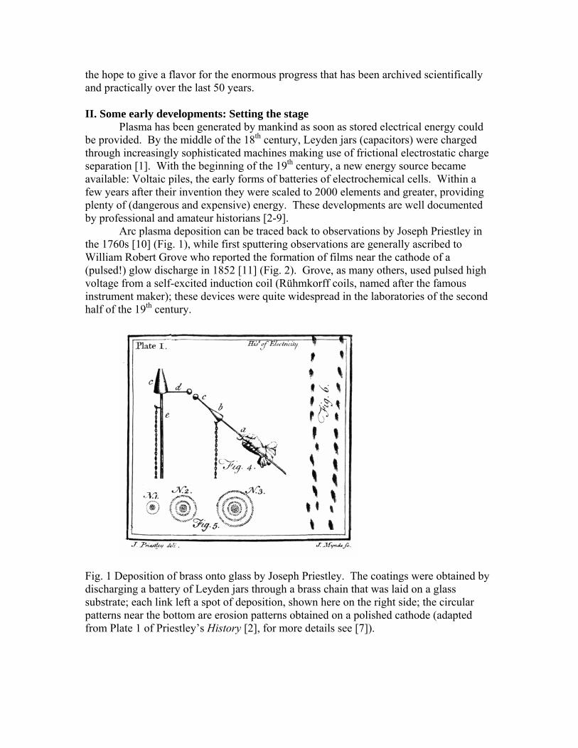
Arc plasma deposition can be traced back to observations by Joseph Priestley in the 1760s [10] (Fig. 1), while first sputtering observations are generally ascribed to William Robert Grove who reported the formation of films near the cathode of a (pulsed!) glow discharge in 1852 [11] (Fig. 2). Grove, as many others, used pulsed high voltage from a self-excited induction coil (Rühmkorff coils, named after the famous instrument maker); these devices were quite widespread in the laboratories of the second half of the 19th century.
Fig. 1 Deposition of brass onto glass by Joseph Priestley. The coatings were obtained by discharging a battery of Leyden jars through a brass chain that was laid on a glass substrate; each link left a spot of deposition, shown here on the right side; the circular patterns near the bottom are erosion patterns obtained on a polished cathode (adapted from Plate 1 of Priestley’s History [2], for more details see [7]).
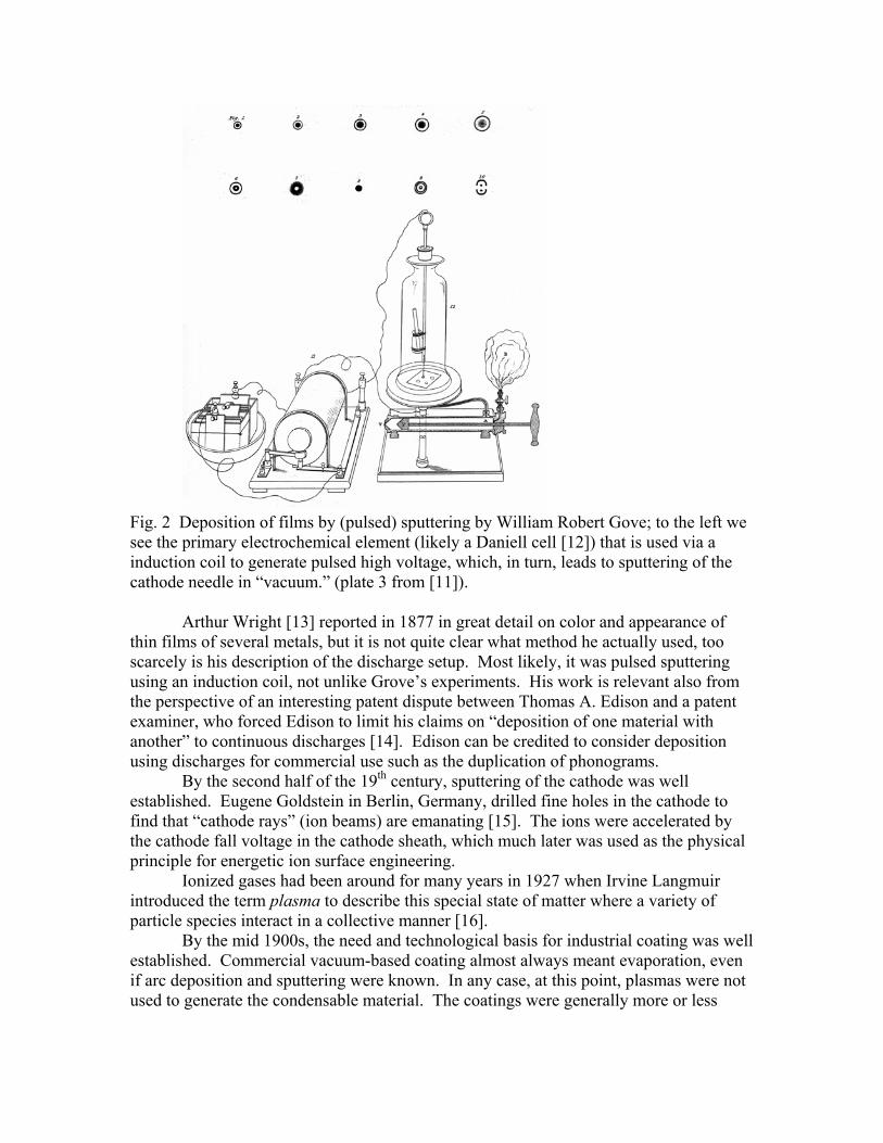
Fig. 2 Deposition of films by (pulsed) sputtering by William Robert Gove; to the left we see the primary electrochemical element (likely a Daniell cell [12]) that is used via a induction coil to generate pulsed high voltage, which, in turn, leads to sputtering of the cathode needle in “vacuum.” (plate 3 from [11]).
Arthur Wright [13] reported in 1877 in great detail on color and appearance of
thin films of several metals, but it is not quite clear what method he actually used, too scarcely is his description of the discharge setup. Most likely, it was pulsed sputtering using an induction coil, not unlike Grove’s experiments. His work is relevant also from the perspective of an interesting patent dispute between Thomas A. Edison and a patent examiner, who forced Edison to limit his claims on “deposition of one material with another” to continuous discharges [14]. Edison can be credited to consider deposition using discharges for commercial use such as the duplication of phonograms.
By the second half of the 19th century, sputtering of the cathode was well established. Eugene Goldstein in Berlin, Germany, drilled fine holes in the cathode to find that “cathode rays” (ion beams) are emanating [15]. The ions were accelerated by the cathode fall voltage in the cathode sheath, which much later was used as the physical principle for energetic ion surface engineering.
Ionized gases had been around for many years in 1927 when Irvine Langmuir introduced the term plasma to describe this special state of matter where a variety of particle species interact in a collective manner [16].
By the mid 1900s, the need and technological basis for industrial coating was well established. Commercial vacuum-based coating almost always meant evaporation, even if arc deposition and sputtering were known. In any case, at this point, plasmas were not used to generate the condensable material. The coatings were generally more or less
porous and adhesion must have been less than perfect. The effects of plasma particles and beams were not yet explored.
III. Ion plating
An interesting prolog to ion plating occurred in the late 1930s when the German B. Berghaus explored the use of plasma and bias to the growth of coatings. Several patents were issued but apparently the field was not ripe to take and utilize these advances [17-19].
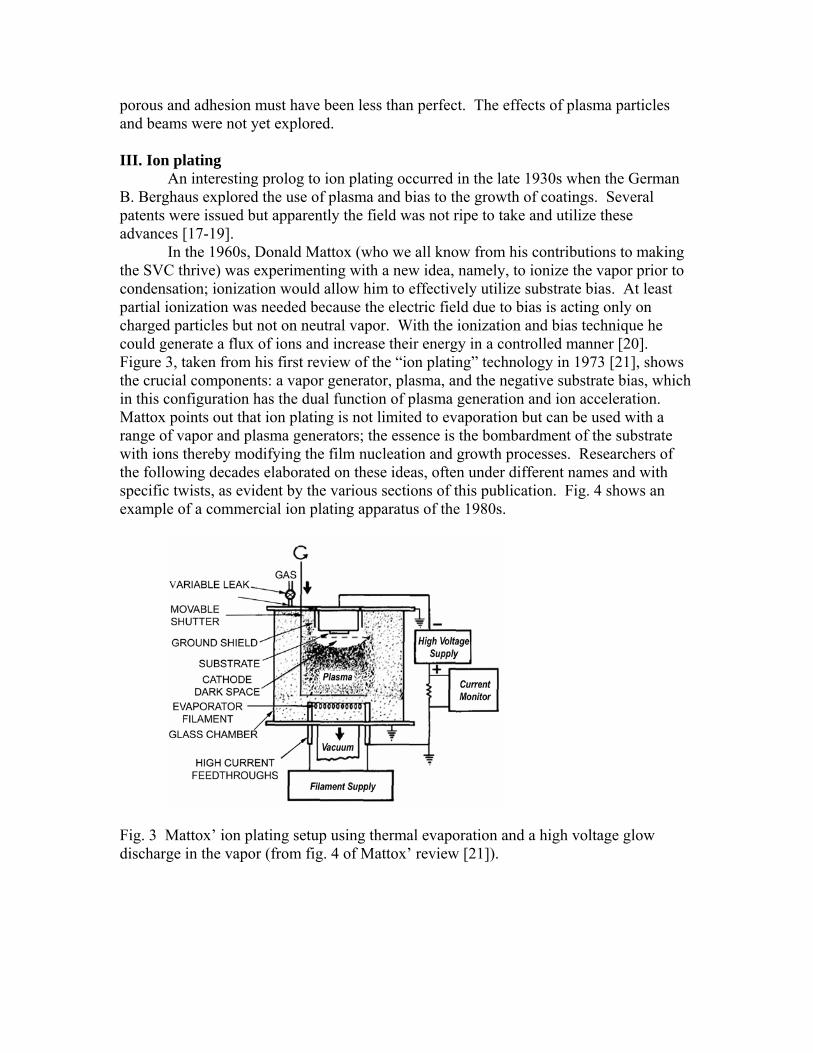
In the 1960s, Donald Mattox (who we all know from his contributions to making the SVC thrive) was experimenting with a new idea, namely, to ionize the vapor prior to condensation; ionization would allow him to effectively utilize substrate bias. At least partial ionization was needed because the electric field due to bias is acting only on charged particles but not on neutral vapor. With the ionization and bias technique he could generate a flux of ions and increase their energy in a controlled manner [20]. Figure 3, taken from his first review of the “ion plating” technology in 1973 [21], shows the crucial components: a vapor generator, plasma, and the negative substrate bias, which in this configuration has the dual function of plasma generation and ion acceleration. Mattox points out that ion plating is not limited to evaporation but can be used with a range of vapor and plasma generators; the essence is the bombardment of the substrate with ions thereby modifying the film nucleation and growth processes. Researchers of the following decades elaborated on these ideas, often under different names and with specific twists, as evident by the various sections of this publication. Fig. 4 shows an example of a commercial ion plating apparatus of the 1980s.
Fig. 3 Mattox’ ion plating setup using thermal evaporation and a high voltage glow discharge in the vapor (from fig. 4 of Mattox’ review [21]).

Fig. 4 1980s vintage industrial reactive ion plating apparatus BAP800 by Balzers. An argon plasma source operated with 55V, 55 A, biased with respect to the electron-beam evaporator, was used to partially ionize the vapor from the evaporator; the system was mainly used to produce optical oxide films of high quality (adapted from [22]).
More recently, evaporation has been demonstrated with very high power, up to
300 kW, and the vapor was ionized using a high current thermionic arc. This thermionic rod activated deposition (RAD) technique was demonstrated for large-area, high-rate aluminum coatings [23].
Yet another incarnation of ion plating is to evaporate and ionize cathode material by an arc operating in the so-called spotless (thermionic) mode. This mode occurs if a region of the cathode has sufficiently high temperature such as to both thermionically emit electrons and to produce sufficient vapor. The spotless mode has been observed to exist for some materials in a self-sustained manner on thermally isolated cathodes, or it can be supported by auxiliary electron beam heating. Spotless arc deposition (SAD) was demonstrated in the 1990s as an industrial process for titanium with rates up to 1 µm/s [24].
IV. Ion Beam Assisted Deposition (IBAD)
In the 1960s, Movchan and Demchishin [25] published a structure zone diagram which essentially had only the substrate temperature as a free parameter. They came from the evaporation world where kinetic energy of condensing particles could not be controlled. A great extension of the zone diagram concept to sputter deposition was done by John A. Thornton [26] who added the sputtering pressure, which essentially is an energy axis (lower pressure implies higher kinetic energy). In the 1980s, the thermodynamically controlled growth (via temperature) and non-equilibrium growth (via kinetic energy) was taken to the next level by adding an ion beam from a dedicated source; the work is summarized in the handbook by J.J. Cuomo, Steve Rossnagel, and Harold Kaufman [27].
Back in 1968/69, sponsored by the former NASA Electronics Research Center, Sol Aisenberg and associates worked on ion beam assisted deposition of thin silicon-based films for electronic device fabrication [28]. Due to some difficulty with stoichiometry issues, he replaced the silicon cathode by carbon and found amorphous, transparent, hard, and inert films, which he called diamond-like carbon [29]. Aisenberg

clearly understood the connection to ion plating and emphasized the common physics in his original papers [30], showing a vapor source and an ion beam source (Fig. 5).
Fig. 5 Ion Beam Assisted Deposition (IBAD) apparatus as shown by Aisenberg and Chabot in 1973 (adapted from [30]).
The importance of ion assistance for film densification was deeper understood
when simulation codes and personal computers became available in the 1980s. In their 1985 book on energetic ion-solid interaction, Ziegler, Biersack and Littmark described computationally efficient approaches using a rather accurate interaction potential [31] (the codes became known as TRIM – transport and range of ions in matter, a modern version can be found at http://www.srim.org ). The TRIM code was originally devised as an aid to understand ion implantation, though soon relatively “low energies” of arriving ions were considered (“low energy” in the sense of ion implantation, e.g. 1 keV or less, is rather high energy for surface and materials scientists).
For example, Karl-Heinz Müller of CSIRO in Sydney, Australia, published a number of papers in 1980s elucidating the individual processes in ion-assisted deposition such as the appearance of collisional cascades, adatom motion, formation of vacancies and interstitials, sputtering, and film densification [22, 32, 33]. All of these properties are important, and of special interest was densification and its effect on the properties of optical coatings (Fig. 6).

Fig. 6 Two-dimensional molecular dynamics simulation of ion beam assisted deposition of titanium vapor, assuming no ion assistance (top), 16% of arriving particles are argon and titanium ions with 50 eV (center and bottom, respectively; adapted from [22]).
V. Direct Plasma/Ion beam deposition
In this section, ions are not just used to assist in the film growth but an ion beam of condensable species can be used. Here, the review crosses over to chemical vapor deposition (CVD). The condensing ions can be generated by decomposition and ionization in a plasma (plasma-assisted CVD), or a dedicated ion source can be used to produce the beam of ions.
A very early example is the largely forgotten work by Heinz Schmellenmeier who worked in Potsdam, East Germany, in the 1950s. He studied the effects of carbon ions on cobalt-doped tungsten cathodes in an acetylene glow discharge. Near the end of his report [34] he mentions that “if the current density is too small [for the diffusion of carbon and the formation of tungsten carbide], a shiny black layer is formed on the cathode, which has initially great adherence but delaminates after hours or days….This layer is extraordinarily hard. With low loads of 10 and 20 g, the layer will not be attacked by a sharp diamond tip…this material is X-ray amorphous...” In a short follow-up paper [35] he adds: “The layers were a few µm thick. Further Laue investigations of flakes that came off showed a cubic structure…and Debye Scherrer pictures gave two strong diamond lines, but the strong graphite lines did not appear.” While his first paper may suggest that he produced DLC, his second indicates that the diamond phase was present, i.e., that he had come across a diamond-CVD process. In any case, Schmellenmeier was at the verge of finding a potentially revolutionizing coatings technology. He published his results in German only and it took another 15 or so years to (re-)discover diamond-like carbon [29] and CVD for diamond films [36, 37].
Gridded [38] and gridless [39] ion sources have been used to bring fluxes of ionized species directly to a substrate surface [40]. Much of the initial ion source development work was done for the original Russian and U.S. space programs, where ion thrusters were developed for satellite propulsion [41]. When applied to thin film deposition, the most interesting and relevant process gases included silane and other silicon-containing gases for semiconductor applications, and hydrocarbon gases for ion beam deposition of protective coatings.
Radio-frequency (RF) glow discharges, including inductively coupled discharges [42, 43], became popular for the decomposition of silicon-containing precursor gases to deposit hydrogenated amorphous silicon [44], which was (and still is) of importance to photovoltaic cells.
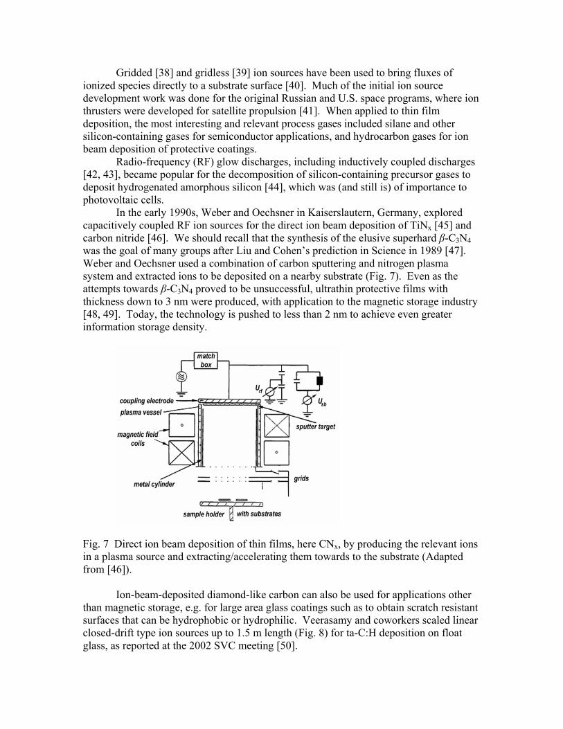
In the early 1990s, Weber and Oechsner in Kaiserslautern, Germany, explored capacitively coupled RF ion sources for the direct ion beam deposition of TiNx [45] and carbon nitride [46]. We should recall that the synthesis of the elusive superhard β-C3N4 was the goal of many groups after Liu and Cohen’s prediction in Science in 1989 [47]. Weber and Oechsner used a combination of carbon sputtering and nitrogen plasma system and extracted ions to be deposited on a nearby substrate (Fig. 7). Even as the attempts towards β-C3N4 proved to be unsuccessful, ultrathin protective films with thickness down to 3 nm were produced, with application to the magnetic storage industry [48, 49]. Today, the technology is pushed to less than 2 nm to achieve even greater information storage density.
Fig. 7 Direct ion beam deposition of thin films, here CNx, by producing the relevant ions in a plasma source and extracting/accelerating them towards to the substrate (Adapted from [46]).
Ion-beam-deposited diamond-like carbon can also be used for applications other
than magnetic storage, e.g. for large area glass coatings such as to obtain scratch resistant surfaces that can be hydrophobic or hydrophilic. Veerasamy and coworkers scaled linear closed-drift type ion sources up to 1.5 m length (Fig. 8) for ta-C:H deposition on float glass, as reported at the 2002 SVC meeting [50].
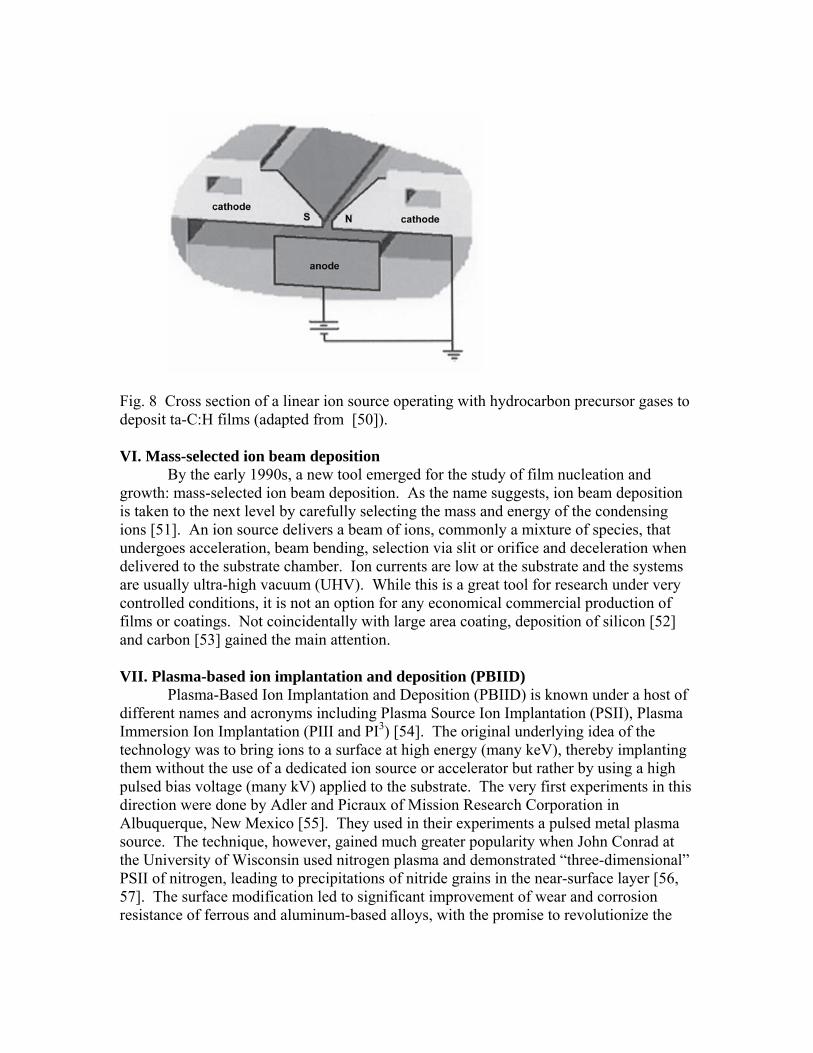
Fig. 8 Cross section of a linear ion source operating with hydrocarbon precursor gases to deposit ta-C:H films (adapted from [50]).
VI. Mass-selected ion beam deposition
By the early 1990s, a new tool emerged for the study of film nucleation and growth: mass-selected ion beam deposition. As the name suggests, ion beam deposition is taken to the next level by carefully selecting the mass and energy of the condensing ions [51]. An ion source delivers a beam of ions, commonly a mixture of species, that undergoes acceleration, beam bending, selection via slit or orifice and deceleration when delivered to the substrate chamber. Ion currents are low at the substrate and the systems are usually ultra-high vacuum (UHV). While this is a great tool for research under very controlled conditions, it is not an option for any economical commercial production of films or coatings. Not coincidentally with large area coating, deposition of silicon [52] and carbon [53] gained the main attention.
VII. Plasma-based ion implantation and deposition (PBIID)
Plasma-Based Ion Implantation and Deposition (PBIID) is known under a host of different names and acronyms including Plasma Source Ion Implantation (PSII), Plasma Immersion Ion Implantation (PIII and PI3) [54]. The original underlying idea of the technology was to bring ions to a surface at high energy (many keV), thereby implanting them without the use of a dedicated ion source or accelerator but rather by using a high pulsed bias voltage (many kV) applied to the substrate. The very first experiments in this direction were done by Adler and Picraux of Mission Research Corporation in Albuquerque, New Mexico [55]. They used in their experiments a pulsed metal plasma source. The technique, however, gained much greater popularity when John Conrad at the University of Wisconsin used nitrogen plasma and demonstrated “three-dimensional” PSII of nitrogen, leading to precipitations of nitride grains in the near-surface layer [56, 57]. The surface modification led to significant improvement of wear and corrosion resistance of ferrous and aluminum-based alloys, with the promise to revolutionize the
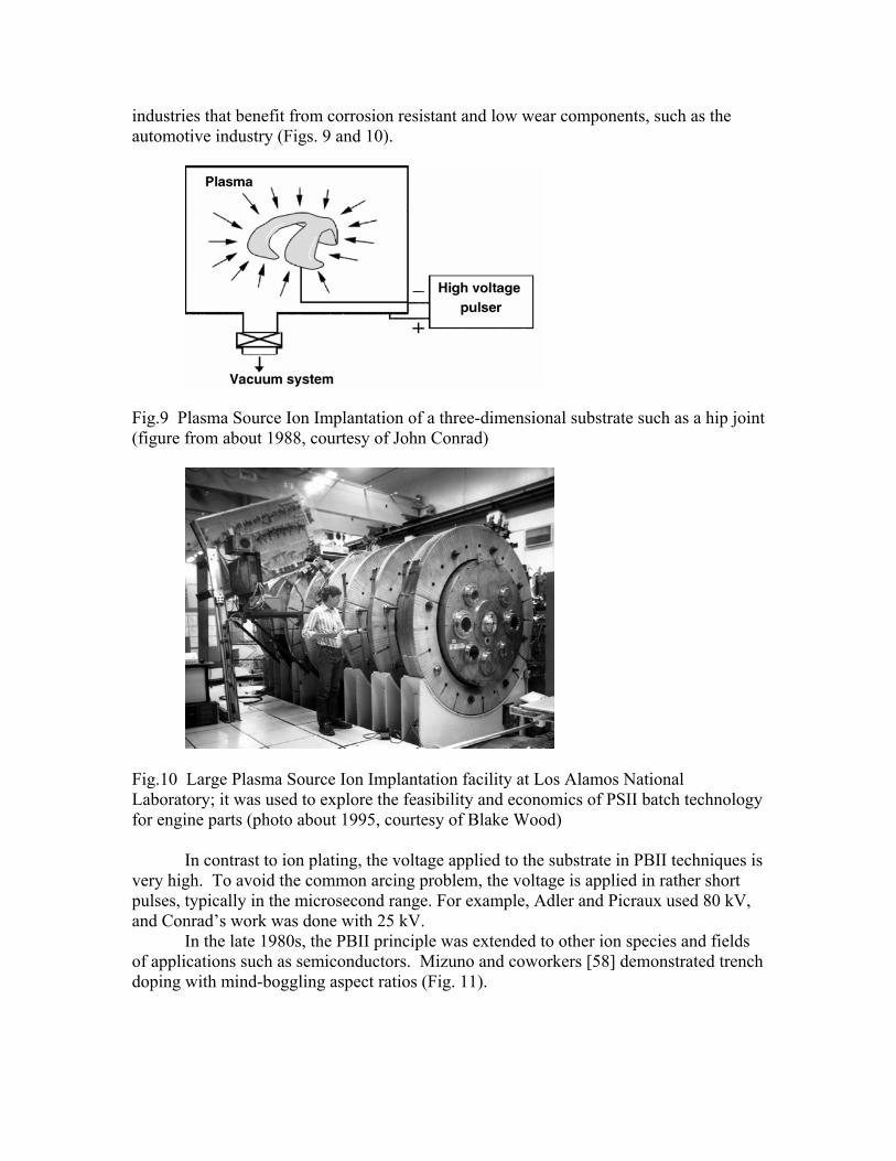
industries that benefit from corrosion resistant and low wear components, such as the automotive industry (Figs. 9 and 10).
Fig.9 Plasma Source Ion Implantation of a three-dimensional substrate such as a hip joint (figure from about 1988, courtesy of John Conrad)
Fig.10 Large Plasma Source Ion Implantation facility at Los Alamos National Laboratory; it was used to explore the feasibility and economics of PSII batch technology for engine parts (photo about 1995, courtesy of Blake Wood)
In contrast to ion plating, the voltage applied to the substrate in PBII techniques is
very high. To avoid the common arcing problem, the voltage is applied in rather short pulses, typically in the microsecond range. For example, Adler and Picraux used 80 kV, and Conrad’s work was done with 25 kV.
In the late 1980s, the PBII principle was extended to other ion species and fields of applications such as semiconductors. Mizuno and coworkers [58] demonstrated trench doping with mind-boggling aspect ratios (Fig. 11).

Fig.11 Plasma immersion ion implantation into a 1 µm wide trench with depth/width aspect ratio of 12:1 using BF3 ECR-plasma and bias of 7.5 kV (photo about 1987, courtesy of Bunji Mizuno).
Paul Chu, Nathan Cheung, and others used energetic plasma immersion ions to
engineer sub-100 nm p+/n junctions [59, 60] and subsurface layers for silicon-on-insulator (SOI) applications [61].
Since then it has become clear that the PBII techniques should be limited to 20 kV or less because otherwise most energy is wasted to secondary electrons which in turn produce unwanted X-rays. In the lower energy regime, the combination with deposition appeared as a fruitful field, where the resulting coatings are characterized by controlled stress [62], adhesion, and—in some materials—preferred orientation of grains [63]. In that sense, PBIID techniques became conceptually very similar to ion plating and ion beam assisted deposition. VIII. Cathodic arc and filtered arc deposition
Cathodic arcs take a special place among the physical vapor deposition techniques because the “vapor” is (almost) fully ionized right from the “birth” at cathode spots. Therefore, any bias applied to a substrate has a great effect without the need for further ionization or plasma production. Arc deposition, attractive for its high deposition rates for the hard and golden TiN, became an industrial process in the 1970s in the Soviet Union and elsewhere in the 1980s. Because there is a companion paper [64] on this technology, no further elaboration is needed here.
IX. Metal ion etch in Arc Bond Sputtering (ABS)
Cathodic arcs were initially used mainly with titanium cathodes to produce the popular TiN coating. By the early 1980s it was realized by Clark Bergman and others that the very high degree of ionization could facilitate ion etching of parts when a high bias is applied, typically –1000 V; e.g., the process starts with using titanium ions and high bias (surface preparation) and continues with nitrogen in the mix at much lower bias voltage

to form TiN [65]. The idea to replace argon ion etching by metal ion etching prior to the deposition step was a few years later transferred to magnetron sputter deposition by Wolf-Dieter Münz [66] in a process called “arc bond sputtering” (ABSTM). This process uses steered arcs and unbalanced sputter magnetrons in large batch coating systems and has become a commercial process [67, 68].
X. Pulsed Laser Deposition (PLD)
Pulsed laser deposition was first explored in the late 1960s, as soon as powerful pulsed lasers became available [69, 70]. The technique experienced a renaissance in the late 1980s for the fabrication of high temperature superconducting films like YBa2Cu3O3-
x (“YBCO”) [71], which can be used in superconducting quantum interference devices, SQIDs. In PLD, practically all materials can be ablated, including insulators, and the stoichiometry of the target is approximately transferred to the film. PLD is now widely used for a range of complex materials such as manganites in colossal magnetoresistive (CMR) devices, ferroelectric materials, multiferroics, etc. High quality films can be obtained, for example crystalline ZnO [72] or doped ZnO and GaN films [73]. The technique is listed here because, not unlike pulsed filtered arcs, the plume of ablated material is typically highly ionized and therefore substrate bias can be applied to influence ion energy.
XI. Anodic arcs and hot refractory anode arcs
Yet another way to generate metal plasma and thereby enable ion assistance via substrate biasing is to utilize the fact that arc anodes tend to become very hot due to heating by electrons. Each electron delivers kinetic energy plus the work function. By not cooling the anode, the temperature can be high enough either to vaporize anode material, as done for the anodic vacuum arc in the late 1980s [74, 75]), or to re-evaporate cathode material, as demonstrated for the hot refractory anode arc in the late 1990s [76, 77].
XII. Ionized physical vapor deposition (i-PVD)
The general concept of ion plating was reborn with the need to meet the challenging demands of integrated circuit metallization in the 1990s. Conventional magnetron sputtering failed when the feature size shrunk to 500 nm, and it was completely unsuitable for the 90-65 nm feature generation. The need for providing a highly directed beam of condensing particles with well-controlled energy was recognized. Acceleration of sputtered particles in one direction was needed, which could be accomplished by bias acceleration if the sputtered atoms were ionized. That was the driving force for the development of ionized physical vapor deposition (i-PVD) [78-80].
In i-PVD, the target material is sputtered at relatively high pressure such as to slow down the sputtered atoms (they have typically several eV of kinetic energy when they leave the surface [81]). Only thermalized atoms have a reasonably high likelihood of ionization by a post-sputtering ionization mechanism such as by an inductively coupled plasma (Fig. 12). The ions diffuse to the sheath edge of the biased substrate, where they are accelerated and deposited into trenches and vias [82].

Fig. 12 Ionized PVD, here with a sputtering process to produce the desired metal
atoms, followed by post-sputtering ionization in an RF inductively coupled plasma.
XIII. Metal Plasma Immersion Ion Implantation and Deposition (MePIIID) Plasma Immersion Ion Implantation with metal plasmas was demonstrated by
Adler and Picraux [55], as already mentioned, but a very similar system can also be used to produce coatings in a hybrid ion implantation and deposition process. The high bias voltage is simply applied for only a fraction of the time. If bias is present, ions are implanted, and with no or low bias, metal ions condense and form a film. Ian Brown and coworkers [83, 84] pioneered this approach and formed a number of well adherent hard films, including compound films [85] and tetrahedral amorphous carbon (ta-C), the hardest in the family of diamond-like carbon (DLC) coatings [86]. For better quality, the process is done with filtered arc plasma, greatly reducing the so-called macroparticle contamination [87]. Most spectacular results were obtained by Peter Siemroth [88] and Othon Monteiro [89] who in the mid 1990s demonstrated sub-micron conformal trench coating and filling (Fig. 13).
Fig. 13 Conformal coating of sub-micron trenches in silicon by tantalum, obtained from a pulsed tantalum filtered arc plasma and bias (photo courtesy of Peter Siemroth).
XIV. High power impulse magnetron sputtering (HIPIMS)
While i-PVD requires additional gadgets for post-sputtering ionization, and cathodic arcs and MePIIID needs to deal with macroparticles using filters or other hardware, there is the desire to produce ionized sputtered material without additional equipment in the processing chamber. HIPIMS promises to deliver this by providing very high power density to the sputtering plasma, causing significant increase in electron temperature and plasma density (the term HIPIMS is used here, as opposed to high power pulsed magnetron sputtering, HPPMS, because the latter term is sometimes used for medium-frequency, large area sputtering, where the power is high but the power density is not).
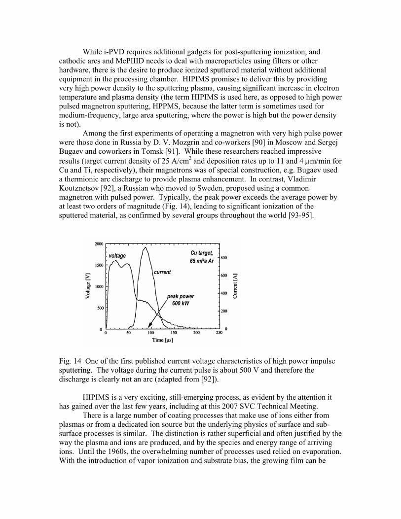
Among the first experiments of operating a magnetron with very high pulse power were those done in Russia by D. V. Mozgrin and co-workers [90] in Moscow and Sergej Bugaev and coworkers in Tomsk [91]. While these researchers reached impressive results (target current density of 25 A/cm2 and deposition rates up to 11 and 4 µm/min for Cu and Ti, respectively), their magnetrons was of special construction, e.g. Bugaev used a thermionic arc discharge to provide plasma enhancement. In contrast, Vladimir Koutznetsov [92], a Russian who moved to Sweden, proposed using a common magnetron with pulsed power. Typically, the peak power exceeds the average power by at least two orders of magnitude (Fig. 14), leading to significant ionization of the sputtered material, as confirmed by several groups throughout the world [93-95].
Fig. 14 One of the first published current voltage characteristics of high power impulse sputtering. The voltage during the current pulse is about 500 V and therefore the discharge is clearly not an arc (adapted from [92]).
HIPIMS is a very exciting, still-emerging process, as evident by the attention it has gained over the last few years, including at this 2007 SVC Technical Meeting.
There is a large number of coating processes that make use of ions either from plasmas or from a dedicated ion source but the underlying physics of surface and sub-surface processes is similar. The distinction is rather superficial and often justified by the way the plasma and ions are produced, and by the species and energy range of arriving ions. Until the 1960s, the overwhelming number of processes used relied on evaporation. With the introduction of vapor ionization and substrate bias, the growing film can be

bombarded by ions, leading to drastic modification of the atomistic processes and film microstructure. Since the introduction of ion plating in the 1960s, there is a stream of new inventions for processes using ions. The development is far from being concluded given the increasing need of surface engineering on the one hand and the new possibilities of plasma diagnostics, materials characterization, and computer modeling on the other. For another, and wider view on the history of physical vapor deposition the reader is referred to Don Mattox’ insightful review [9]. Acknowledgement
This work was supported by the Assistant Secretary for Energy Efficiency and Renewable Energy, Office of Building Technology, of the U.S. Department of Energy under Contract No. DE-AC02-05CH11231.
References
[1] V. E. Johnson, Modern High-Speed Influence Machines. London: E.&F.N. Spon Ltd, 1922. [2] J. Priestley, The History and Present State of Electricity, 3rd ed. London, 1775. [3] P. Dahl, Flash of the Cathode Ray. A History of J J Thomson's Electron. Bristol: Institute of Physics Publishing, 1997. [4] B. Bowers, A History of Electric Light and Power. London: Peter Peregrinus Ltd., 1991. [5] J. L. Heilbron, Electricity in the 17th and 18th Centuries. Mineola, New York: Dover Publications, 1999. [6] B. Dibner, Galvani - Volta. A Controversy that led to the Discovery of Useful Electricity. Norwalk, Conneticut: Burndy Library, 1952. [7] A. Anders, IEEE Trans. Plasma Sci. 31 (2003) 1052. [8] A. Anders, IEEE Trans. Plasma Sci. 31 (2003) 1060. [9] D. M. Mattox, The history of vacuum coating technology. Albuquerque: Society of Vacuum Coaters, 2002. [10] J. Priestley, “Experiments in which rings, consisting of all the prismatic colours, where made by electrical explosions on the surface of metals,” in The History and Present State of Electricity, vol. II. London, 1775, 329-335. [11] W. R. Grove, Phil. Trans. Roy. Soc. London 142 (1852) 87. [12] J. F. Daniell, (Poggendorff's) Annalen der Physik und Chemie 66 (1843) 376. [13] A. W. Wright, Am. J. Science & Arts, 3rd Series 13 (1877) 49. [14] T. A. Edison, US 526,147: Art of plating one material with another, Patent U.S. 526,147, Sept. 18, 1894, filed January 28, 1884 1894. [15] E. Goldstein, Sitzungsberichte der Königlichen Akademie der Wissenschaften zu Berlin 39 (1886) 691. [16] H. M. Mott-Smith, Nature 233 (1971) 219. [17] B. Berghaus, German Patent No. 668,639, Patent 668,639, 1938. [18] B. Berghaus, UK Patent 510,993: Improvements in and relating to the coating of articles by means of thermally vaporized material, Patent UK 510,993, 1938.

[19] B. Berghaus and W. Burkhardt, Patent US 2305758: Improvements in and relating to the coating of articles by means of thermally vaporized material, filed April 22, 1938, Patent 1942. [20] D. M. Mattox, Electrochem. Technol. 2 (1964) 295. [21] D. M. Mattox, J. Vac. Sci. Technol. 10 (1973) 47. [22] K. H. Guenther, B. Loo, D. Burns, J. Edgell, D. Windham, and K.-H. Müller, J. Vac. Sci. Technol. A 7 (1989) 1436. [23] B. Scheffel, C. Metzner, K. Goedicke, J.-P. Heinss, and O. Zywitzki, Surf. Coat. Technol. 120-121 (1999) 718. [24] K. Goedicke, B. Scheffel, and S. Schiller, Surf. Coat. Technol. 68-69 (1994) 799. [25] B. A. Movchan and A. V. Demchishin, Fizika Metallov i Metallovedenie (Physics of Metals and Metallography) 28 (1969) 653. [26] J. A. Thornton, J. Vac. Sci. Technol. 11 (1974) 666. [27] J. J. Cuomo, S. M. Rossnagel, and H. R. Kaufman, (Ed.), Handbook of Ion Beam Processing Technology. Park Ridge, NJ: Noyes, 1989. [28] F. M. Kimock, D. W. Brown, S. J. Finke, and E. Thear, datatech no. 2 (1999) 69. [29] S. Aisenberg and R. Chabot, J. Appl. Phys. 42 (1971) 2953. [30] S. Aisenberg and R. W. Chabot, J. Vac. Sci. Technol. 10 (1973) 104. [31] J. F. Ziegler, J. P. Biersack, and U. Littmark, The Stopping and Range of Ions in Solids. New York: Pergamon Press, 1985. [32] K.-H. Müller, J. Appl. Phys. 59 (1986) 2803. [33] K.-H. Müller, Appl. Phys. A 40 (1986) 209. [34] H. Schmellenmeier, Experimentelle Technik der Physik 1 (1953) 49. [35] H. Schmellenmeier, Zeitschrift für Physikalische Chemie 205 (1956) 349. [36] J. E. Field, (Ed.), The Properties of Diamond. London: Academic Press, 1979. [37] J. Asmussen and D. Reinhard, (Ed.), Diamond Films Handbook. New York: Marcel Dekker, 2002. [38] H. R. Kaufman and R. S. Robinson, “Gridded broad-beam ion sources,” in Handbook of Ion Beam Processing Technology, J. J. Cuomo, S. M. Rossnagel, and H. R. Kaufman, Eds. Park Ridge: Noyes, 1989, 8-20. [39] H. R. Kaufman, R. S. Robinson, and R. I. Seddon, J. Vac. Sci. Technol. A 5 (1987) 2081. [40] A. T. Forrester, Large Ion Beams. New York: Wiley, 1988. [41] E. Y. Choueiri, J. Propulsion and Power 20 (2004) 193. [42] J. C. Knights, Phil. Mag. 34 (1976) 663. [43] H. Fritzsche, M. Tanielian, C. C. Tsai, and P. J. Gaczi, J. Appl. Phys. 50 (1979) 3366. [44] J. L. Andujar, E. Bertran, A. Canillas, J. Esteve, J. Andreau, and J. L. Morenza, Vacuum 39 (1989) 795. [45] F. R. Weber and H. Oechsner, Surf. Coat. Technol. 59 (1993) 234. [46] F. R. Weber and H. Oechsner, Surf. Coat. Technol. 74-75 (1995) 704. [47] A. Y. Liu and M. L. Cohen, Science 245 (1989) 841. [48] E. V. Anoikin, M. M. Yang, J. L. Chao, and M. A. Russak, J. Appl. Phys. 85 (1999) 5606. [49] J. Robertson, Thin Solid Films 383 (2001) 81.

[50] V. S. Veerasamy, R. H. Petrlichl, H. A. Luten, and S. V. Thomsen, “Large area ion-beam deposition of hydrogenated tetrahedral amorphous carbon on soda-lime glass,” 45th Annual Technical Conference, Society of Vacuum Coaters, Lake Buena Vista, FL, 2002, 127-134. [51] D. G. Armour, Nucl. Instr. Meth. B 89 (1994) 325. [52] A. H. Al-Bayati, K. J. Boyd, D. Marton, S. S. Todorov, J. W. Rabalais, Z. H. Zhang, and W. K. Chu, J. Appl. Phys. 76 (1994) 4383. [53] J. Kulik, Y. Lifshitz, G. D. Lempert, J. W. Rabalais, and D. Marton, J. Appl. Phys. 76 (1994) 5063. [54] A. Anders, (Ed.), Handbook of Plasma Immersion Ion Implantation and Deposition. New York: John Wiley & Sons, 2000. [55] R. J. Adler and S. T. Picraux, Nucl. Instrum. Meth. Phys. Res. B 6 (1985) 123. [56] J. R. Conrad, J. L. Radtke, R. A. Dodd, F. J. Worzala, and N. C. Tran, J. Appl. Phys. 62 (1987) 4591. [57] J. R. Conrad, R. A. Dodd, F. J. Worzala, and X. Qiu, Surf. Coat. Technol. 36 (1988) 927. [58] B. Mizuno, I. Nakayama, N. Aoi, M. Kubota, and T. Komeda, Appl. Phys. Lett. 53 (1988) 2059. [59] N. W. Cheung, Nucl. Instrum. Methods B 55 (1991) 811. [60] E. C. Jones and N. W. Cheung, IEEE Elec. Dev. Lett. 14 (1993) 444. [61] P. K. Chu, X. Lu, S. S. K. Iyer, and N. W. Cheung, Solid State Technol. 40 (1997) S9. [62] M. M. M. Bilek and D. R. McKenzie, Surf. Coat. Technol. 200 (2006) 4345. [63] S. H. N. Lim, D. G. McCulloch, M. M. M. Bilek, and D. R. McKenzie, J. Appl. Phys. 93 (2003) 4283. [64] A. Anders, “A brief modern history of cathodic arc coating,” The 50th SVC Annual Technical Conference of the Society of Vacuum Coaters, Louisville, KY, 2007, [65] C. Bergman, “Arc plasma physical vapor deposition,” 28th Annual SVC Technical Conference, Philadelphia, PA, 1985, 175-191. [66] W.-D. Münz, D. Schulze, and F. J. M. Hauzer, Surf. Coat. Technol. 50 (1992) 169. [67] A. P. Ehiasarian, P. E. Hovsepian, L. Hultman, and U. Helmersson, Thin Solid Films 457 (2004) 270. [68] D. B. Lewis, D. Reitz, C. Wüstefeld, R. Ohser-Wiedemann, H. Oettel, A. P. Ehiasarian, and P. E. Hovsepian, Thin Solid Films 503 (2006) 133. [69] D. B. Chrisey and G. K. Hubler, (Ed.), Pulsed Laser Deposition of Thin Films. New York: Wiley, 1994. [70] R. Eason, Pulsed Laser Deposition of Thin Films: Applications-Led Growth of Functional Materials Wiley, 2007. [71] A. Inam, M. S. Hegde, X. D. Wu, T. Venkatesan, P. England, P. F. Miceli, E. W. Chase, C. C. Chang, J. M. Tarascon, and J. B. Wachtman, Appl. Phys. Lett. 53 (1988) 908. [72] P. Misra and L. M. Kukreja, Thin Solid Films 485 (2005) 42. [73] L. S. Dorneles, D. O'Mahony, C. B. Fitzgerald, F. McGee, M. Venkatesan, I. Stanca, J. G. Lunney, and J. M. D. Coey, Appl. Surf. Sci. 248 (2005) 406. [74] H. Ehrich, J. Vac. Sci. Technol. A 6 (1988) 134.
[75] H. Ehrich, B. Hasse, M. Mausbach, and K. G. Müller, IEEE Trans. Plasma Sci. 18 (1990) 895. [76] I. I. Beilis, R. L. Boxman, S. Goldsmith, and V. L. Paperny, J. Appl. Phys. 88 (2000) 6224. [77] I. I. Beilis, A. Shashurin, R. L. Boxman, and S. Goldsmith, Appl. Phys. Lett. 88 (2006) 71501. [78] S. R. Rossnagel and J. Hopwood, J. Vac. Sci. Technol. B 12 (1994) 449. [79] J. Hopwood, Phys. Plasmas 5 (1998) 1624. [80] M. J. Grapperhaus, Z. Krivokapic, and M. J. Kushner, J. Appl. Phys. 83 (1998) 35. [81] V. I. Shulga, Nucl. Instrum. Meth. Phys. Res. B 179 (2001) 485. [82] J. A. Hopwood, (Ed.), Ionized Physical Vapor Deposition. San Diego, CA: Academic Press, 2000. [83] I. G. Brown, X. Godechot, and K. M. Yu, Appl. Phys. Lett. 58 (1991) 1392. [84] I. G. Brown, A. Anders, S. Anders, M. R. Dickinson, I. C. Ivanov, R. A. MacGill, X. Y. Yao, and K.-M. Yu, Nucl. Instrum. Meth. Phys. Res. B 80/81 (1993) 1281. [85] A. Anders, S. Anders, I. G. Brown, M. R. Dickinson, and R. A. MacGill, J. Vac. Sci. Technol. B 12 (1994) 815. [86] S. Anders, A. Anders, I. G. Brown, B. Wei, K. Komvopoulos, J. W. Ager, and K. M. Yu, Surf. Coat. Technol. 68/69 (1994) 388. [87] A. Anders, Surf. Coat. Technol. 93 (1997) 157. [88] P. Siemroth, C. Wenzel, W. Kliomes, B. Schultrich, and T. Schülke, Thin Solid Films 308 (1997) 455. [89] O. R. Monteiro, J. Vac. Sci. Technol. B 17 (1999) 1094. [90] D. V. Mozgrin, I. K. Fetisov, and G. V. Khodachenko, Plasma Phys. Rep. 21 (1995) 400. [91] S. P. Bugaev, N. N. Koval, N. S. Sochugov, and A. N. Zakharov, “Investigation of a high-current pulsed magentron discharge initiated in the low-pressure diffuse arc plasma,” XVIIth Int. Symp. Discharges and Electrical Insulation in Vacuum, Berkeley, CA, 1996, 1074-1076. [92] V. Kouznetsov, K. Macak, J. M. Schneider, U. Helmersson, and I. Petrov, Surf. Coat. Technol. 122 (1999) 290. [93] A. P. Ehiasarian, R. New, W.-D. Münz, L. Hultman, U. Helmersson, and V. Kouznetsov, Vacuum 65 (2002) 147. [94] J. Bohlmark, J. Alami, C. Christou, A. Ehiasarian, and U. Helmersson, J. Vac. Sci. Technol. A 23 (2005) 18. [95] J. Vlček, P. Kudláček, K. Burcalová, and J. Musil, Eur. Phys. Lett. 77 (2007) 45002.