Embed Size (px)
Citation preview

3Planning Pin and FPGA Resources
2013.12.16
emi_dg_003 Subscribe Send Feedback
This information is for board designers who need to determine the FPGA pin usage, to create the boardlayout for the system, as the board design process sometimes occurs concurrently with the RTL designprocess.
Use this document with the External Memory Interfaces chapter of the relevant device family handbook.
Typically, all external memory interfaces require the following FPGA resources:
• Interface pins• PLL and clock network• DLL• Other FPGA resources—for example, core fabric logic, and on-chip termination (OCT) calibration blocks
After you know the requirements for your memory interface, you can start planning your system. The I/Opins and internal memory cannot be shared for other applications or memory interfaces. However, if youdo not have enough PLLs, DLLs, or clock networks for your application, you may share these resourcesamong multiple memory interfaces or modules in your system.
Ideally, any interface should reside entirely in a single bank; however, interfaces that span multiple adjacentbanks or the entire side of a device are also fully supported. In addition, you may also have wraparoundmemory interfaces, where the design uses two adjacent sides of the device and the memory interface logicresides in a device quadrant. In some cases, top or bottom bank interfaces have higher supported clock ratethan left or right or wraparound interfaces.
Interface PinsAny I/O banks that do not support transceiver operations in Arria® II, Arria V, Stratix® III, Stratix IV, andStratix V devices support memory interfaces. However, DQS (data strobe or data clock) and DQ (data) pinsare listed in the device pin tables and fixed at specific locations in the device. You must adhere to these pinlocations as these locations are optimized in routing to minimize skew and maximize margin. Always checkthe external memory interfaces chapters from the device handbooks for the number of DQS and DQ groupssupported in a particular device and the pin table for the actual locations of the DQS and DQ pins.
For maximum performance and best skew across the interface, each required memory interface shouldcompletely reside within a single I/O bank, or at least one side of the device. Address and command pinscan be constrained in a different side of the device if there are not enough pins available. For example, youmay have the read and write data pins on the top side of the device, and have the address and commandpins on the left side of the device. In memory interfaces with unidirectional data, you may also have all the
ISO9001:2008Registered
© 2013 Altera Corporation. All rights reserved. ALTERA, ARRIA, CYCLONE, HARDCOPY, MAX, MEGACORE, NIOS, QUARTUS and STRATIX wordsand logos are trademarks of Altera Corporation and registered in the U.S. Patent and Trademark Office and in other countries. All otherwords and logos identified as trademarks or service marks are the property of their respective holders as described atwww.altera.com/common/legal.html. Altera warrants performance of its semiconductor products to current specifications in accordance withAltera's standard warranty, but reserves the right to make changes to any products and services at any time without notice. Altera assumesno responsibility or liability arising out of the application or use of any information, product, or service described herein except as expresslyagreed to in writing by Altera. Altera customers are advised to obtain the latest version of device specifications before relying on any publishedinformation and before placing orders for products or services.
www.altera.com
101 Innovation Drive, San Jose, CA 95134

read data pins on the top side of the device and the write data pin on the left side of the device. However,you should not break a unidirectional pin group across multiple sides of the device. Memory interfacestypically have the following pin groups:
• Write data pin group and read data pin group• Address and command pin group
The following table lists a summary of the number of pins required for various example memory interfaces.This table uses series OCT with calibration, parallel OCT with calibration, or dynamic calibrated OCT, whenapplicable, shown by the usage of RUP and RDN pins or RZQ pin.
Table 3-1: Pin Counts for Various Example Memory Interfaces (1) (2)
Total Pinswith RZQ
TotalPinswith
RUP/RDN
RZQPins(11)
RUP/RDN
Pins (4)
Numberof
ClockPins
Numberof
CommandPins
Numberof
AddressPins (3)
Numberof DM/BWSnPins
Numberof DQS
Pins
Numberof DQPins
FPGADQSBus
Width
MemoryInterface
26N/A1N/A2210128
×8LPDDR2 37N/A1N/A22102416
114N/A1N/A221091872
333412210140 (7)24×4
DDR3SDRAM(5) (6)
38391221014128
×8 495012210142416
133134124141491872
33341229151 (7)14×4
DDR2SDRAM(8)
373812291511 (9)8
×8 474812291522 (9)16
124125126121599 (9)72
28291227141 (7)14×4
DDRSDRAM(6)
3533122714118
×8 42431227142216
1171181269139972
48491243 (10)191218×9QDRII+SRAM
66671243 (10)182236×18
1031041243 (10)174272×36
Planning Pin and FPGA ResourcesAltera Corporation
Send Feedback
emi_dg_003Interface Pins3-2 2013.12.16

Total Pinswith RZQ
TotalPinswith
RUP/RDN
RZQPins(11)
RUP/RDN
Pins (4)
Numberof
ClockPins
Numberof
CommandPins
Numberof
AddressPins (3)
Numberof DM/BWSnPins
Numberof DQS
Pins
Numberof DQPins
FPGADQSBus
Width
MemoryInterface
47481242191218×9QDR IISRAM 65661242182236×18
1021031242174272×36
46471247 (10)22129×9RLDRAM
II CIO 56571267 (10)211218
75761287 (10)201236×18
Notes to table:
1. These example pin counts are derived from memory vendor data sheets. Check the exact number ofaddresses and command pins of the memory devices in the configuration that you are using.
2. PLL and DLL input reference clock pins are not counted in this calculation.3. The number of address pins depend on the memory device density.4. Some DQS or DQ pins are dual purpose and can also be required as RUP, RDN, or configuration pins. A
DQS group is lost if you use these pins for configuration or as RUP or RDN pins for calibrated OCT. PickRUP and RDN pins in a DQS group that is not used for memory interface purposes. You may need to placethe DQS and DQ pins manually if you place the RUP and RDN pins in the same DQS group pins.
5. The TDQS and TDQS# pins are not counted in this calculation, as these pins are not used in the memorycontroller.
6. Numbers are based on 1-GB memory devices.7. Altera® FPGAs do not support DM pins in ×4 mode with differential DQS signaling.8. Numbers are based on 2-GB memory devices without using differential DQS, RDQS, and RDQS# pin
support.9. Assumes single ended DQS mode. DDR2 SDRAM also supports differential DQS, which makes these
DQS and DM numbers identical to DDR3 SDRAM.10. The QVLD pin that indicates read data valid from the QDR II+ SRAM or RLDRAM II device, is included
in this number.11. RZQ pins are supported by Arria V, Cyclone V, and Stratix V devices.
Maximum interface width varies from device to device depending on the number of I/O pins andDQS or DQ groups available. Achievable interface width also depends on the number of address and
Note:
command pins that the design requires. To ensure adequate PLL, clock, and device routing resourcesare available, you should always test fit any IP in the Quartus® II software before PCB sign-off.
Altera devices do not limit the width of external memory interfaces beyond the following requirements:
• Maximum possible interface width in any particular device is limited by the number of DQS groupsavailable.
• Sufficient clock networks are available to the interface PLL as required by the IP.• Sufficient spare pins exist within the chosen bank or side of the device to include all other address and
command, and clock pin placement requirements.• The greater the number of banks, the greater the skew, hence Altera recommends that you always generate
a test project of your desired configuration and confirm that it meets timing.
Altera CorporationPlanning Pin and FPGA Resources
Send Feedback
3-3Interface Pinsemi_dg_0032013.12.16

Estimating Pin requirementsYou should use the Quartus II software for final pin fitting; however, you can estimate whether you haveenough pins for your memory interface using the following steps:
1. Find out how many read data pins are associated per read data strobe or clock pair, to determine whichcolumn of the DQS and DQ group availability (×4, ×8/×9, ×16/×18, or ×32/×36) look at the pin table.
2. Check the device density and package offering information to see if you can implement the interface inone I/O bank or on one side or on two adjacent sides.
If you target Arria II GX devices and you do not have enough I/O pins to have the memoryinterface on one side of the device, you may place them on the other side of the device. Arria II
Note:
GX devices allow a memory interface to span across the top and bottom, or left and right sidesof the device. For any interface that spans across two different sides, use the wraparound interfaceperformance.
3. Calculate the number of other memory interface pins needed, including any other clocks (write clock ormemory system clock), address, command, RUP, RDN, RZQ, and any other pins to be connected to thememory components. Ensure you have enough pins to implement the interface in one I/O bank or oneside or on two adjacent sides.
The DQS groups in Arria II GX devices reside on I/O modules, each consisting of 16 I/O pins.You can only use a maximum of 12 pins per I/O modules when the pins are used as DQS or DQ
Note:
pins or HSTL/SSTL output or HSTL/SSTL bidirectional pins. When counting the number ofavailable pins for the rest of your memory interface, ensure you do not count the leftover fourpins per I/O modules used for DQS, DQ, address and command pins. The leftover four pins canbe used as input pins only.
Refer to the device pin-out tables and look for the blank space in the relevant DQS group columnto identify the four pins that cannot be used in an I/O module for Arria II GX devices.
Note:
You should always try the proposed pin-outs with the rest of your design in the Quartus II software (withthe correct I/O standard and OCT connections) before finalizing the pin-outs, as there may be someinteractions between modules that are illegal in the Quartus II software that you may not find out unlessyou try compiling a design and use the Quartus II Pin Planner.
The following sections describe the pins for each memory interfaces.
DDR, DDR2, and DDR3 SDRAM Clock SignalsDDR, DDR2, and DDR3 SDRAM devices use CK and CK# signals to clock the address and command signalsinto the memory. Furthermore, the memory uses these clock signals to generate the DQS signal during aread through the DLL inside the memory. The SDRAM data sheet specifies the following timings:
• tDQSCK is the skew between the CK or CK# signals and the SDRAM-generated DQS signal• tDSH is the DQS falling edge from CK rising edge hold time• tDSS is the DQS falling edge from CK rising edge setup time• tDQSS is the positive DQS latching edge to CK rising edge
These SDRAM have a write requirement (tDQSS) that states the positive edge of the DQS signal on writesmust be within ± 25% (± 90°) of the positive edge of the SDRAM clock input. Therefore, you should generatethe CK and CK# signals using the DDR registers in the IOE to match with the DQS signal and reduce anyvariations across process, voltage, and temperature. The positive edge of the SDRAM clock, CK, is alignedwith the DQS write to satisfy tDQSS.
Planning Pin and FPGA ResourcesAltera Corporation
Send Feedback
emi_dg_003Estimating Pin requirements3-4 2013.12.16

DDR3 SDRAM can use a daisy-chained control address command (CAC) topology, in which the memoryclock must arrive at each chip at a different time. To compensate for this flight-time skew between devicesacross a typical DIMM, write leveling must be employed.
DDR, DDR2, and DDR3 SDRAM Command and Address SignalsCommand and address signals in SDRAM devices are clocked into the memory device using the CK or CK#signal. These pins operate at single data rate (SDR) using only one clock edge. The number of address pinsdepends on the SDRAM device capacity. The address pins are multiplexed, so two clock cycles are requiredto send the row, column, and bank address.
The CS#, RAS, CAS, WE, CKE, and ODT pins are SDRAM command and control pins. DDR3 SDRAM hasan additional pin, RESET#, while some DDR3 DIMMs have these additional pins: RESET#, PAR_IN, andERR_OUT#. The RESET# pin uses the 1.5-V LVCMOS I/O standard, and the PAR_IN and ERR_OUT#pins use the SSTL-15 I/O standard.
The DDR2 SDRAM command and address inputs do not have a symmetrical setup and hold time requirementwith respect to the SDRAM clocks, CK, and CK#.
For Altera SDRAM high-performance controllers in Stratix III and Stratix IV devices, the command andaddress clock is a dedicated PLL clock output whose phase can be adjusted to meet the setup and holdrequirements of the memory clock. The command and address clock is also typically half-rate, although afull-rate implementation can also be created. The command and address pins use the DDIO output circuitryto launch commands from either the rising or falling edges of the clock. The chip select (mem_cs_n), clockenable (mem_cke), and ODT (mem_odt) pins are only enabled for one memory clock cycle and can belaunched from either the rising or falling edge of the command and address clock signal. The address andother command pins are enabled for two memory clock cycles and can also be launched from either therising or falling edge of the command and address clock signal.
In Arria II GX devices, the command and address clock is either shared with the write_clk_2x or themem_clk_2x clock.
DDR, DDR2, and DDR3 SDRAM Data, Data Strobes, DM, and Optional ECC SignalsDDR SDRAM uses bidirectional single-ended data strobe (DQS); DDR3 SDRAM uses bidirectional differentialdata strobes. The DQSn pins in DDR2 SDRAM devices are optional but recommended for DDR2 SDRAMdesigns operating at more than 333 MHz. Differential DQS operation enables improved system timing dueto reduced crosstalk and less simultaneous switching noise on the strobe output drivers. The DQ pins arealso bidirectional.
Regardless of interface width, DDR SDRAM always operates in ×8 mode DQS groups. DQ pins in DDR2and DDR3 SDRAM interfaces can operate in either ×4 or ×8 mode DQS groups, depending on your chosenmemory device or DIMM, regardless of interface width. The ×4 and ×8 configurations use one pair ofbidirectional data strobe signals, DQS and DQSn, to capture input data. However, two pairs of data strobes,UDQS and UDQS# (upper byte) and LDQS and LDQS# (lower byte), are required by the ×16 configurationdevices. A group of DQ pins must remain associated with its respective DQS and DQSn pins.
The DQ signals are edge-aligned with the DQS signal during a read from the memory and are center-alignedwith the DQS signal during a write to the memory. The memory controller shifts the DQ signals by –90degrees during a write operation to center align the DQ and DQS signals. The PHY IP delays the DQS signalduring a read, so that the DQ and DQS signals are center aligned at the capture register. Altera devices usea phase-locked loop (PLL) to center-align the DQS signal with respect to the DQ signals during writes andAltera devices use dedicated DQS phase-shift circuitry to shift the incoming DQS signal during reads. Thefollowing figure shows an example where the DQS signal is shifted by 90 degrees for a read from the DDR2SDRAM.
Altera CorporationPlanning Pin and FPGA Resources
Send Feedback
3-5DDR, DDR2, and DDR3 SDRAM Command and Address Signalsemi_dg_0032013.12.16

Figure 3-1: Edge-aligned DQ and DQS Relationship During a DDR2 SDRAM Read in Burst-of-Four Mode
DQS at DQIOE registers
DQS atFPGA Pin
DQ at DQIOE registers
DQ atFPGA Pin
DQS phase shift
Preamble Postamble
The following figure shows an example of the relationship between the data and data strobe during a burst-of-four write.
Figure 3-2: DQ and DQS Relationship During a DDR2 SDRAM Write in Burst-of-Four Mode
DQS atFPGA Pin
DQ atFPGA Pin
The memory device's setup (tDS) and hold times (tDH) for the write DQ and DM pins are relative to the edgesof DQS write signals and not the CK or CK# clock. Setup and hold requirements are not necessarily balancedinDDR2 and DDR3 SDRAM, unlike in DDR SDRAM devices.
The DQS signal is generated on the positive edge of the system clock to meet the tDQSS requirement. DQand DM signals use a clock shifted –90 from the system clock, so that the DQS edges are centered on theDQ or DM signals when they arrive at the DDR2 SDRAM. The DQS, DQ, and DM board trace lengths needto be tightly matched (within 20 ps).
The SDRAM uses the DM pins during a write operation. Driving the DM pins low shows that the write isvalid. The memory masks the DQ signals if the DM pins are driven high. To generate the DM signal, Alterarecommends that you use the spare DQ pin within the same DQS group as the respective data, to minimizeskew.
The DM signal's timing requirements at the SDRAM input are identical to those for DQ data. The DDRregisters, clocked by the –90 degree shifted clock, create the DM signals.
Some SDRAM modules support error correction coding (ECC) to allow the controller to detect andautomatically correct error in data transmission. The 72-bit SDRAM modules contain eight extra data pinsin addition to 64 data pins. The eight extra ECC pins should be connected to a single DQS or DQ group onthe FPGA.
DDR, DDR2, and DDR3 SDRAM DIMM OptionsUnbuffered DIMMs (UDIMMs) require one set of chip-select (CS#), on-die termination (ODT), clock-enable(CKE#), and clock pair (CK/CKn) for every physical rank on the DIMM. Registered DIMMs use only onepair of clocks and require a minimum of two chip-select signals, even in the case of a single rank RDIMM.
Planning Pin and FPGA ResourcesAltera Corporation
Send Feedback
emi_dg_003DDR, DDR2, and DDR3 SDRAM DIMM Options3-6 2013.12.16

Compared to the unbuffered DIMMs (UDIMM), registered and load-reduced DIMMs (RDIMMs andLRDIMMs, respectively) use only one pair of clocks and at least two chip-select signalsCS#[1:0] in DDR3.Both RDIMMs and LRDIMMs require an additional parity signal for address, RAS, CAS, and WE signals.
Unbuffered DIMMs require unique chip-select, ODT, CKE, and clock pair signals for every rank on theDIMM. RDIMMs differ slightly in that only one clock pair is required for the entire module and a minimumof two chip select signals must be present (even for single-rank DIMMs) for programming of the RDIMMbuffer.
LRDIMMs expand on the operation of RDIMMs by buffering the DQ/DQS bus. Only one electrical load ispresented to the controller regardless of the number of ranks, therefore only one clock enable and ODTsignal are required for LRDIMMs, regardless of the number of physical ranks. Because the number of physicalranks may exceed the number of physical chip-select signals, LRDIMMs provide a feature known as rankmultiplication, which aggregates two or four physical ranks into one larger logical rank. Refer to LRDIMMbuffer documentation for details on rank multiplication.
Both RDIMMs and LRDIMMs require an additoinal parity input for address,RAS#,CAS#, andWE# signals.A parity error signal is asserted by the module whenever a parity error is detected.
The following table shows UDIMM and RDIMM pin options.
Table 3-2: UDIMM and RDIMM Pin Options
RDIMM Pins
(Dual Rank)
RDIMM Pins (Single Rank)UDIMM Pins
(Dual Rank)
UDIMM Pins (Single Rank)Pins
72 bit DQ[71:0]=
{CB[7:0],DQ[63:0]}
72 bit DQ[71:0] =
{CB[7:0],DQ[63:0]}
72 bit DQ[71:0] =
{CB[7:0],DQ[63:0]}
72 bit DQ[71:0] =
{CB[7:0],DQ[63:0]}
Data
DM[8.0]DM[8.0]DM[8.0]DM[8:0]DataMask
DQS[8:0] andDQS#[8:0]
DQS[8:0] andDQS#[8:0]
DQS[8:0] andDQS#[8:0]
DQS[8:0] andDQS#[8:0]
DataStrobe(1)
BA[2:0],A[15:0]–
2 GB: A[13:0]
4 GB: A[14:0]
8 GB: A[15:0]
BA[2:0], A[15:0]–2 GB: A[13:0]
4 GB: A[14:0]
8 GB: A[15:0]
BA[2:0], A[15:0]–
2 GB: A[13:0]
4 GB: A[14:0]
8 GB: A[15:0]
BA[2:0], A[15:0]–
2 GB: A[13:0]
4 GB: A[14:0]
8 GB: A[15:0]
Address
CK0/CK0#CK0/CK0#CK0/CK0#, CK1/CK1#CK0/CK0#Clock
ODT[1:0],CS#[1:0],CKE[1:0], RAS#,CAS#, WE#
ODT, CS#[1:0], CKE,RAS#, CAS#, WE#
ODT[1:0],CS#[1:0],CKE[1:0], RAS#,CAS#, WE#
ODT, CS#, CKE, RAS#,CAS#, WE#
Command
PAR_IN, ERR_OUTPAR_IN, ERR_OUT——Parity
Altera CorporationPlanning Pin and FPGA Resources
Send Feedback
3-7DDR, DDR2, and DDR3 SDRAM DIMM Optionsemi_dg_0032013.12.16

RDIMM Pins
(Dual Rank)
RDIMM Pins (Single Rank)UDIMM Pins
(Dual Rank)
UDIMM Pins (Single Rank)Pins
SA[2:0], SDA,SCL, EVENT#,RESET#
SA[2:0], SDA, SCL,EVENT#, RESET#
SA[2:0], SDA, SCL,EVENT#, RESET#
SA[2:0], SDA, SCL,EVENT#, RESET#
OtherPins
Note to Table:
1. DQS#[8:0] is optional in DDR2 SDRAM and is not supported in DDR SDRAM interfaces.
The following table shows LRDIMM pin options.
Table 3-3: LRDIMM Pin Options
LDIMM Pins (8R,RM=4)
LRDIMM Pins (8R,RM=2)
LRDIMM Pins (4R,RM=2)
LRDIMM (4R, RM=1)LRDIMM Pins (2R)Pins
72 bit DQ[71:0]={CB[7:0], DQ[63:0]}
72 bit DQ[71:0]={CB [7:0],DQ [63:0]}
72 bit DQ[71:0]={CB [7:0],DQ [63:0]}
72 bit DQ[71:0]={CB [7:0],DQ [63:0]}
72 bit DQ[71:0]={CB [7:0],DQ [63:0]}
Data
—————DataMask
DQS[17:0] andDQS#[17:0]
DQS[17:0] andDQS#[17:0]
DQS[17:0] andDQS#[17:0]
DQS[17:0] andDQS#[17:0]
DQS[17:0] andDQS#[17:0]
DataStrobe
BA[2:0],A[17:0]-16GB:A[15:0]32GB:A[16:0]64GB:A[17:0]
BA[2:0], A[16:0]-4GB:A[14:0]8GB:A[15:0]16GB:A[16:0]
BA[2:0], A[16:0]-4GB:A[14:0]8GB:A[15:0]16GB:A[16:0]
BA[2:0], A[15:0]-2GB:A[13:0]4GB:A[14:0]8GB:A[15:0]
BA[2:0], A[15:0]-2GB:A[13:0]4GB:A[14:0]8GB:A[15:0]
Address
CK0/CK0#CK0/CK0#CK0/CK0#CK0/CK0#CK0/CK0#Clock
ODT, CS[1:0]#,CKE, RAS#,CAS#, WE#
ODT, CS[3:0]#,CKE, RAS#, CAS#,WE#
ODT, CS[1:0]#,CKE, RAS#, CAS#,WE#
ODT, CS[3:0]#,CKE, RAS#, CAS#,WE#
ODT, CS[1:0]#,CKE, RAS#, CAS#,WE#
Command
PAR_IN,ERR_OUT
PAR_IN, ERR_OUT
PAR_IN, ERR_OUT
PAR_IN, ERR_OUT
PAR_IN, ERR_OUT
Parity
SA[2:0], SDA,SCL, EVENT#,RESET#
SA[2:0], SDA, SCL,EVENT#, RESET#
SA[2:0], SDA, SCL,EVENT#, RESET#
SA[2:0], SDA, SCL,EVENT#, RESET#
SA[2:0], SDA, SCL,EVENT#, RESET#
OtherPins
Notes to Table:
1. DM pins are not used for LRDIMMs because they are constructed using ×4 components for greatermemory density.
2. CS2# is treated as A[16] and CS3# is treated as A[17] for certain rank multiplication configurations.Consult LRDIMM documentation for details.
Planning Pin and FPGA ResourcesAltera Corporation
Send Feedback
emi_dg_003DDR, DDR2, and DDR3 SDRAM DIMM Options3-8 2013.12.16

QDR II+ and QDR II SRAM Clock SignalsQDR II+ and QDR II SRAM devices have three pairs of clocks, listed below.
• Input clocks K and K#• Input clocks C and C#• Echo clocks CQ and CQ#
The positive input clock, K, is the logical complement of the negative input clock, K#. Similarly, C and CQare complements of C# and CQ#, respectively. With these complementary clocks, the rising edges of eachclock leg latch the DDR data.
The QDR II+ and QDR II SRAM devices use the K and K# clocks for write access and the C and C# clocksfor read accesses only when interfacing more than one QDR II+ or QDR II SRAM device. Because the numberof loads that the K and K# clocks drive affects the switching times of these outputs when a controller drivesa single QDR II+ or QDR II SRAM device, C and C# are unnecessary. This is because the propagation delaysfrom the controller to the QDR II+ or QDR II SRAM device and back are the same. Therefore, to reducethe number of loads on the clock traces, QDR II+ and QDR II SRAM devices have a single clock mode, andthe K and K# clocks are used for both reads and writes. In this mode, the C and C# clocks are tied to thesupply voltage (VDD).
CQ and CQ# are the source-synchronous output clocks from the QDR II or QDR II+ SRAM device thataccompanies the read data.
The Altera device outputs the K and K# clocks, data, address, and command lines to the QDR II+ or QDRII SRAM device. For the controller to operate properly, the write data (D), address (A), and control signaltrace lengths (and therefore the propagation times) should be equal to the K and K# clock trace lengths.
You can generate C, C#, K, and K# clocks using any of the PLL registers via the DDR registers. Because ofstrict skew requirements between K and K# signals, use adjacent pins to generate the clock pair. Thepropagation delays for K and K# from the FPGA to the QDR II+ or QDR II SRAM device are equal to thedelays on the data and address (D, A) signals. Therefore, the signal skew effect on the write and read requestoperations is minimized by using identical DDR output circuits to generate clock and data inputs to thememory.
QDR II+ and QDR II SRAM Command SignalsQDR II+ and QDR II SRAM devices use the write port select (WPSn) signal to control write operations andthe read port select (RPSn) signal to control read operations.
The byte write select signal (BWSn) is a third control signal that indicates to the QDR II+ or QDR II SRAMdevice which byte to write into the QDR II+ or QDR II SRAM device. You can use any of the FPGA's userI/O pins to generate control signals, preferably on the same side and the same bank. Assign the BWSn pinwithin the same DQS group as the corresponding the write data.
QDR II+ and QDR II SRAM Address SignalsQDR II+ and QDR II SRAM devices use one address bus (A) for both read and write addresses. You can useany of the FPGA's user I/O pins to generate address signals, preferably on the same side and the same banks.
QDR II+ and QDR II SRAM Data and QVLD SignalsQDR II+ and QDR II SRAM devices use two unidirectional data buses: one for writes (D) and one for reads(Q).
The read data is edge-aligned with the CQ and CQ# clocks while the write data is center-aligned with the Kand K# clocks (see the following figures).
Altera CorporationPlanning Pin and FPGA Resources
Send Feedback
3-9QDR II+ and QDR II SRAM Clock Signalsemi_dg_0032013.12.16

Figure 3-3: Edge-aligned CQ and Q Relationship During QDR II+ SRAM Read
CQ# atFPGA Pin
CQ atFPGA Pin
Q atFPGA Pin
CQ atCapture Register
CQ# atCapture Register
Q atCapture Register
DQS phaseshift
Figure 3-4: Center-aligned K and D Relationship During QDR II+ SRAM Write
K# atFPGA Pin
K atFPGA Pin
D atFPGA Pin
QDR II+ SRAM devices also have a QVLD pin that indicates valid read data. The QVLD signal is edge-aligned with the echo clock and is asserted high for approximately half a clock cycle before data is outputfrom memory.
The Altera QDR II+ SRAM Controller with UniPHY IP does not use the QVLD signal.Note:
RLDRAM II and RLDRAM 3 Clock SignalsRLDRAM II and RLDRAM 3 devices use CK and CK# signals to clock the command and address bus insingle data rate (SDR). There is one pair of CK and CK# pins per RLDRAM II or RLDRAM 3 device.
Instead of a strobe, RLDRAM II and RLDRAM 3 devices use two sets of free-running differential clocks toaccompany the data. The DK and DK# clocks are the differential input data clocks used during writes whilethe QK or QK# clocks are the output data clocks used during reads. Even though QK and QK# signals are notdifferential signals according to the RLDRAM II and RLDRAM 3 data sheets, Micron treats these signals assuch for their testing and characterization. Each pair of DK and DK#, or QK and QK# clocks are associatedwith either 9 or 18 data bits.
Planning Pin and FPGA ResourcesAltera Corporation
Send Feedback
emi_dg_003RLDRAM II and RLDRAM 3 Clock Signals3-10 2013.12.16
The exact clock-data relationships are as follows:
• RLDRAM II: For ×36 data bus width configuration, there are 18 data bits associated with each pair ofwrite and read clocks. So, there are two pairs of DK and DK# pins and two pairs of QK or QK# pins.
• RLDRAM 3: For ×36 data bus width configuration, there are 18 data bits associated with each pair ofwrite clocks. There are 9 data bits associated with each pair of read clocks. So, there are two pairs of DKand DK# pins and four pairs of QK and QK# pins.
• RLDRAM II: For ×18 data bus width configuration, there are 18 data bits per one pair of write clocksand nine data bits per one pair of read clocks. So, there is one pair of DK and DK# pins, but there are twopairs of QK and QK# pins.
• RLDRAM 3: For ×18 data bus width configuration, there are 9 data bits per one pair of write clocks andnine data bits per one pair of read clocks. So, there are two pairs of DK and DK# pins, and two pairs ofQK and QK# pins
• RLDRAM II: For ×9 data bus width configuration, there are nine data bits associated with each pair ofwrite and read clocks. So, there is one pair of DK and DK# pins and one pair of QK and QK# pins each.
• RLDRAM 3: RLDRAM 3 does not have the ×9 data bus width configuration.
There are tCKDK timing requirements for skew between CK and DK or CK# and DK#.
For both RLDRAM II and RLDRAM 3, because of the loads on these I/O pins, the maximum frequency youcan achieve depends on the number of memory devices you are connecting to the Altera device. PerformSPICE or IBIS simulations to analyze the loading effects of the pin-pair on multiple RLDRAM II devices.
RLDRAM II and RLDRAM 3 Commands and AddressesThe CK and CK# signals clock the commands and addresses into the memory devices.
These pins operate at single data rate using only one clock edge. RLDRAM II and RLDRAM 3 support bothnon-multiplexed and multiplexed addressing. Multiplexed addressing allows you to save a few user I/O pinswhile non-multiplexed addressing allows you to send the address signal within one clock cycle instead oftwo clock cycles. CS#, REF#, and WE# pins are input commands to the RLDRAM II or RLDRAM 3 device.
The commands and addresses must meet the memory address and command setup (tAS, tCS) and hold (tAH,tCH) time requirements.
UniPHY IP does not support multiplexed addressing.Note:
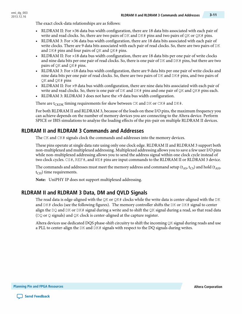
RLDRAM II and RLDRAM 3 Data, DM and QVLD SignalsThe read data is edge-aligned with the QK or QK# clocks while the write data is center-aligned with the DKand DK# clocks (see the following figures). The memory controller shifts the DK or DK# signal to centeralign the DQ and DK or DK# signal during a write and to shift the QK signal during a read, so that read data(DQ or Q signals) and QK clock is center-aligned at the capture register.
Altera devices use dedicated DQS phase-shift circuitry to shift the incoming QK signal during reads and usea PLL to center-align the DK and DK# signals with respect to the DQ signals during writes.
Altera CorporationPlanning Pin and FPGA Resources
Send Feedback
3-11RLDRAM II and RLDRAM 3 Commands and Addressesemi_dg_0032013.12.16
Figure 3-5: Edge-aligned DQ and QK Relationship During RLDRAM II or RLDRAM 3 Read
QK atFPGA Pin
DQ atFPGA Pin
QK at DQLE Registers
DQ at DQLE Registers
DQS Phase Shift
Figure 3-6: Center-aligned DQ and DK Relationship During RLDRAM II or RLDRAM 3 Write
DK atFPGA Pin
DQ atFPGA Pin
For RLDRAM II and RLDRAM 3, data mask (DM) pins are only used during a write. The memory controllerdrives the DM signal low when the write is valid and drives it high to mask the DQ signals. There is one DMpin per memory device.
The DM timing requirements at the input to the memory device are identical to those for DQ data. TheDDR registers, clocked by the write clock, create the DM signals. This reduces any skew between the DQ andDM signals.
The RLDRAM II or RLDRAM 3 device's setup time (tDS) and hold (tDH) time for the write DQ and DM pinsare relative to the edges of the DK or DK# clocks. The DK and DK# signals are generated on the positive edgeof system clock, so that the positive edge of CK or CK# is aligned with the positive edge of DK or DK#respectively to meet the tCKDK requirement. The DQ and DM signals are clocked using a shifted clock sothat the edges of DK or DK# are center-aligned with respect to the DQ and DM signals when they arrive at theRLDRAM II or RLDRAM 3 device.
The clocks, data, and DM board trace lengths should be tightly matched to minimize the skew in the arrivaltime of these signals.
RLDRAM II and RLDRAM 3 devices also have a QVLD pin indicating valid read data. The QVLD signal isedge-aligned with QK or QK# and is high approximately half a clock cycle before data is output from thememory.
The RLDRAM II Controller with UniPHY IP and the RLDRAM 3 PHY-only IP do not use the QVLDsignal.
Note:
LPDDR2 Clock SignalCK and CKn are differential clock inputs to the LPDDR2 interface. All the double data rate (DDR) inputsare sampled on both the positive and negative edges of the clock. Single data rate (SDR) inputs, CSn andCKE, are sampled at the positive clock edge.
Planning Pin and FPGA ResourcesAltera Corporation
Send Feedback
emi_dg_003LPDDR2 Clock Signal3-12 2013.12.16

The clock is defined as the differential pair which consists of CK and CKn. The positive clock edge is definedby the cross point of a rising CK and a falling CKn. The negative clock edge is defined by the cross point ofa falling CK and a rising CKn.
The SDRAM data sheet specifies timing data for the following:
• tDSH is the DQS falling edge hold time from CK.• tDSS is the DQS falling edge to the CK setup time.• tDQSS is the Write command to the first DQS latching transition.• tDQSCK is the DQS output access time from CK_t/CK_c.
LPDDR2 Command and Address SignalAll LPDDR2 devices use double data rate architecture on the command/address bus to reduce the numberof input pins in the system. The 10-bit command/address bus contains command, address, and bank/rowbuffer information. Each command uses one clock cycle, during which command information is transferredon both the positive and negative edges of the clock.
LPDDR2 Data, Data Strobe, and DM SignalsLPDDR2 devices use bidirectional and differential data strobes.
Differential DQS operation enables improved system timing due to reduced crosstalk and less simultaneousswitching noise on the strobe output drivers. The DQ pins are also bidirectional. DQS is edge-aligned duringthe read data and centered during the write data.
DM is the input mask for the write data signal. Input data is masked when DM is sampled high coincidentwith that input data during a write access.
Maximum Number of InterfacesThe maximum number of interfaces supported for a given memory protocol varies, depending on the FPGAin use.
Unless otherwise noted, the calculation for the maximum number of interfaces is based on independentinterfaces where the address or command pins are not shared. The maximum number of independentinterfaces is limited to the number of PLLs each FPGA device has.
You must share DLLs if the total number of interfaces exceeds the number of DLLs available in aspecific FPGA device. You may also need to share PLL clock outputs depending on your clock networkusage, refer to “PLLs and Clock Networks”.
Note:
For information about the number of DQ and DQS in other packages, refer to theDQ andDQS tablesin the relevant device handbook.
Note:
Timing closure depends on device resource and routing utilization. For more information about timingclosure, refer to the Area and Timing Optimization Techniques chapter in the Quartus II Handbook.
Related Information
• Quartus II Handbook
• PLLs and Clock Networks on page 3-45
Altera CorporationPlanning Pin and FPGA Resources
Send Feedback
3-13LPDDR2 Command and Address Signalemi_dg_0032013.12.16

Maximum Number of DDR SDRAM Interfaces Supported per FPGAThe following table describes the maximum number of ×8 DDR SDRAM components fit in the smallest andbiggest devices and pin packages assuming the device is blank.
Each interface of size n, where n is a multiple of 8, consists of:
• n DQ pins (including error correction coding (ECC))• n/8 DM pins• n/8 DQS pins• 18 address pins• 6 command pins (CAS, RAS, WE, CKE, reset, and CS)• 1 CK, CK# pin pair for up to every three ×8 DDR SDRAM components
Table 3-4: Maximum Number of DDR SDRAM Interfaces Supported per FPGA
Maximum Number of InterfacesPackage Pin CountDevice TypeDevice
Four ×8 interfaces or one ×72 interface on eachside (no DQ pins on left side)
1,152EP2AGX190
EP2AGX260
Arria II GX • On top side, one ×16 interface• On bottom side, one ×16 interface• On right side (no DQ pins on left side), one
×8 interface
358EP2AGX45
EP2AGX65
Four ×8 interfaces or one ×72 interface on eachside
F1,517EP2AGZ300
EP2AGZ350
EP2AGZ225
Arria II GZ • On top side, three ×8 interfaces or one ×64interface
• On bottom side, three ×8 interfaces or one×64 interface
• No DQ pins on the left and right sides
F780EP2AGZ300
EP2AGZ350
• Two ×72 interfaces on both top and bottomsides
• One ×72 interface on both right and leftsides
1,760EP3SL340
Stratix III• Two ×8 interfaces on both top and bottom
sides• Three ×8 interface on both right and left
sides
484EP3SE50
Planning Pin and FPGA ResourcesAltera Corporation
Send Feedback
emi_dg_003Maximum Number of DDR SDRAM Interfaces Supported per FPGA3-14 2013.12.16

Maximum Number of InterfacesPackage Pin CountDevice TypeDevice
• One ×72 interface on each side
or
• One ×72 interface on each side and twoadditional ×72 wraparound interfaces, onlyif sharing DLL and PLL resources
1,932EP4SGX290
EP4SGX360
EP4SGX530
Stratix IV
1,760EP4SE530
EP4SE820
• Three ×8 interfaces or one ×64 interface onboth top and bottom sides
• On left side, one ×48 interface or two ×8interfaces
• No DQ pins on the right side
780EP4SGX70
EP4SGX110
EP4SGX180
EP4SGX230
Maximum Number of DDR2 SDRAM Interfaces Supported per FPGAThe following table lists the maximum number of ×8 DDR2 SDRAM components that can be fitted in thesmallest and biggest devices and pin packages assuming the device is blank.
Each interface of size n, where n is a multiple of 8, consists of:
• n DQ pins (including ECC)• n/8 DM pins• n/8 DQS, DQSn pin pairs• 18 address pins• 7 command pins (CAS, RAS, WE, CKE, ODT, reset, and CS)• 1 CK, CK# pin pair up to every three ×8 DDR2 components
Table 3-5: Maximum Number of DDR2 SDRAM Interfaces Supported per FPGA
Maximum Number of InterfacesPackage Pin CountDevice TypeDevice
Four ×8 interfaces or one ×72 interface oneach side (no DQ pins on left side)
1,152EP2AGX190
EP2AGX260
Arria II GX • One ×16 interface on both top and bottomsides
• On right side (no DQ pins on left side),one ×8 interface
358EP2AGX45
EP2AGX65
Four ×8 interfaces or one ×72 interface oneach side
F1,517EP2AGZ300
EP2AGZ350
EP2AGZ225Arria II GZ• Three ×8 interfaces or one ×64 interface
on both top and bottom sides• No DQ pins on the left and right sides
F780EP2AGZ300
EP2AGZ350
Altera CorporationPlanning Pin and FPGA Resources
Send Feedback
3-15Maximum Number of DDR2 SDRAM Interfaces Supported per FPGAemi_dg_0032013.12.16

Maximum Number of InterfacesPackage Pin CountDevice TypeDevice
• Two ×72 interfaces on both top andbottom sides
• No DQ pins on left and right sides
1,5175AGXB1
5AGXB3
5AGXB5
5AGXB7
5AGTD3
5AGTD7Arria V
• One ×56 interface or two x24 interfaceson both top and bottom sides
• One ×32 interface on the right side• No DQ pins on the left side
6725AGXA1
5AGXA3
• One ×56 interface or two x24 interfaceson both top and bottom sides
• No DQ pins on the left side
6725AGXA5
5AGXA7
• Three ×72 interfaces on both top andbottom sides
• No DQ pins on left and right sides
1,5175AGZE5
5AGZE7
Arria V GZ • On top side, two ×8 interfaces• On bottom side, four ×8 interfaces or one
×72 interface• No DQ pins on left and right sides
7805AGZE1
5AGZE3
• One ×72 interface or two ×32 interfaceson each of the top, bottom, and right sides
• No DQ pins on the left side
1,1525CGTD9
5CEA9
5CGXC9Cyclone V
• One ×48 interface or two ×16 interfaceson both top and bottom sides
• One x8 interface on the right side• No DQ pins on the left side
4845CEA7
5CGTD7
5CGXC7
• Two ×72 interfaces on both top andbottom sides
• One ×72 interface on both right and leftsides
1,760EP3SL340
Stratix III• Two ×8 interfaces on both top and bottom
sides• Three ×8 interfaces on both right and left
sides
484EP3SE50
Planning Pin and FPGA ResourcesAltera Corporation
Send Feedback
emi_dg_003Maximum Number of DDR2 SDRAM Interfaces Supported per FPGA3-16 2013.12.16

Maximum Number of InterfacesPackage Pin CountDevice TypeDevice
• One ×72 interface on each side
or
• One ×72 interface on each side and twoadditional ×72 wraparound interfaces onlyif sharing DLL and PLL resources
1,932EP4SGX290
EP4SGX360
EP4SGX530
Stratix IV
1,760EP4SE530
EP4SE820
• Three ×8 interfaces or one ×64 interfaceon top and bottom sides
• On left side, one ×48 interface or two ×8interfaces
• No DQ pins on the right side
780EP4SGX70
EP4SGX110
EP4SGX180
EP4SGX230
• Three ×72 interfaces on both top andbottom sides
• No DQ pins on left and right sides
1,9325SGXA5
5SGXA7
Stratix V • On top side, two ×8 interfaces• On bottom side, four ×8 interfaces or one
×72 interface• No DQ pins on left and right sides
7805SGXA3
5SGXA4
Maximum Number of DDR3 SDRAM Interfaces Supported per FPGAThe following table lists the maximum number of ×8 DDR3 SDRAM components that can be fitted in thesmallest and biggest devices and pin packages assuming the device is blank.
Each interface of size n, where n is a multiple of 8, consists of:
• n DQ pins (including ECC)• n/8 DM pins• n/8 DQS, DQSn pin pairs• 17 address pins• 7 command pins (CAS, RAS, WE, CKE, ODT, reset, and CS)• 1 CK, CK# pin pair
Table 3-6: Maximum Number of DDR3 SDRAM Interfaces Supported per FPGA
Maximum Number of InterfacesPackage PinCount
Device TypeDevice
Four ×8 interfaces or one ×72 interface on each side (no DQpins on left side)
1,152EP2AGX190
EP2AGX260Arria II GX
• One ×16 interface on both top and bottom sides• On right side, one ×8 interface (no DQ pins on left side)
358EP2AGX45
EP2AGX65
Altera CorporationPlanning Pin and FPGA Resources
Send Feedback
3-17Maximum Number of DDR3 SDRAM Interfaces Supported per FPGAemi_dg_0032013.12.16

Maximum Number of InterfacesPackage PinCount
Device TypeDevice
Four ×8 interfaces on each sideF1,517EP2AGZ300
EP2AGZ350
EP2AGZ225Arria II GZ
• Three ×8 interfaces on both top and bottom sides• No DQ pins on left and right sides
F780EP2AGZ300
EP2AGZ350
• Two ×72 interfaces on both top and bottom sides• No DQ pins on left and right sides
1,5175AGXB1
5AGXB3
5AGXB5
5AGXB7
5AGTD3
5AGTD7Arria V
• One ×56 interface or two ×24 interfaces on top and bottomsides
• One ×32 interface on the right side• No DQ pins on the left side
6725AGXA1
5AGXA3
• One ×56 interface or two ×24 interfaces on both top andbottom sides
• No DQ pins on the left side
6725AGXA5
5AGXA7
• Two ×72 interfaces on both top and bottom sides• No DQ pins on left and right sides
1,5175AGZE5
5AGZE7Arria V GZ • On top side, two ×8 interfaces
• On bottom side, four ×8 interfaces• No DQ pins on left and right sides
7805AGZE1
5AGZE3
• One ×72 interface or two ×32 interfaces on each of the top,bottom, and right sides
• No DQ pins on the left side
1,1525CGTD9
5CEA9
5CGXC9Cyclone V
• One ×48 interface or two ×16 interfaces on both top andbottom sides
• One x8 interface on the right side• No DQ pins on the left side
4845CEA7
5CGTD7
5CGXC7
• Two ×72 interfaces on both top and bottom sides• One ×72 interface on both right and left sides
1,760EP3SL340
Stratix III• Two ×8 interfaces on both top and bottom sides• Three ×8 interfaces on both right and left sides
484EP3SE50
Planning Pin and FPGA ResourcesAltera Corporation
Send Feedback
emi_dg_003Maximum Number of DDR3 SDRAM Interfaces Supported per FPGA3-18 2013.12.16

Maximum Number of InterfacesPackage PinCount
Device TypeDevice
• One ×72 interface on each side
or
• One ×72 interface on each side and 2 additional ×72wraparound interfaces only if sharing DLL and PLLresources
1,932EP4SGX290
EP4SGX360
EP4SGX530
Stratix IV
1,760EP4SE530
EP4SE820
• Three ×8 interfaces or one ×64 interface on both top andbottom sides
• On left side, one ×48 interface or two ×8 interfaces (no DQpins on right side)
780EP4SGX70
EP4SGX110
EP4SGX180
EP4SGX230
• Two ×72 interfaces (800 MHz) on both top and bottomsides
• No DQ pins on left and right sides
1,9325SGXA5
5SGXA7
Stratix V• On top side, two ×8 interfaces• On bottom side, four ×8 interfaces• No DQ pins on left and right sides
7805SGXA3
5SGXA4
Maximum Number of QDR II and QDR II+ SRAM Interfaces Supported per FPGAThe following table lists the maximum number of independent QDR II+ or QDR II SRAM interfaces thatcan be fitted in the smallest and biggest devices and pin packages assuming the device is blank.
One interface of ×36 consists of:
• 36 Q pins• 36 D pins• 1 K, K# pin pairs• 1 CQ, CQ# pin pairs• 19 address pins• 4 BSWn pins• WPS, RPS
One interface of ×9 consists of:
• 9 Q pins• 9 D pins• 1 K, K# pin pairs• 1 CQ, CQ# pin pairs• 21 address pins• 1 BWSn pin• WPS, RPS
Altera CorporationPlanning Pin and FPGA Resources
Send Feedback
3-19Maximum Number of QDR II and QDR II+ SRAM Interfaces Supported per FPGAemi_dg_0032013.12.16

Table 3-7: Maximum Number of QDR II and QDR II+ SRAM Interfaces Supported per FPGA
Maximum Number of InterfacesPackage PinCount
Device TypeDevice
One ×36 interface and one ×9 interface one each side1,152EP2AGX190
EP2AGX260Arria II GX
One ×9 interface on each side (no DQ pins on left side)358EP2AGX45
EP2AGX65
• Two ×36 interfaces and one ×9 interface on both top andbottom sides
• Four ×9 interfaces on right and left sides
F1,517EP2AGZ300
EP2AGZ350
EP2AGZ225Arria II GZ
• Three ×9 interfaces on both top and bottom sides• No DQ pins on right and left sides
F780EP2AGZ300
EP2AGZ350
• Two ×36 interfaces on both top and bottom sides• No DQ pins on left and right sides
1,5175AGXB1
5AGXB3
5AGXB5
5AGXB7
5AGTD3
5AGTD7Arria V
• Two ×9 interfaces on both top and bottom sides• One ×9 interface on the right side• No DQ pins on the left side
6725AGXA1
5AGXA3
• Two ×9 interfaces on both top and bottom sides• No DQ pins on the left side
6725AGXA5
5AGXA7
• Two ×36 interfaces on both top and bottom sides• No DQ pins on left and right sides
1,5175AGZE5
5AGZE7Arria V GZ • On top side, one ×36 interface or three ×9 interfaces
• On bottom side, two ×9 interfaces• No DQ pins on left and right sides
7805AGZE1
5AGZE3
• Two ×36 interfaces and one ×9 interface on both top andbottom sides
• Five ×9 interfaces on both right and left sides
1,760EP3SL340
Stratix III • One ×9 interface on both top and bottom sides• Two ×9 interfaces on both right and left sides
484EP3SE50
EP3SL50
EP3SL70
Planning Pin and FPGA ResourcesAltera Corporation
Send Feedback
emi_dg_003Maximum Number of QDR II and QDR II+ SRAM Interfaces Supported per FPGA3-20 2013.12.16
Maximum Number of InterfacesPackage PinCount
Device TypeDevice
• Two ×36 interfaces on both top and bottom sides• One ×36 interface on both right and left sides
1,932EP4SGX290
EP4SGX360
EP4SGX530
Stratix IV
1,760EP4SE530
EP4SE820
Two ×9 interfaces on each side (no DQ pins on right side)780EP4SGX70
EP4SGX110
EP4SGX180
EP4SGX230
• Two ×36 interfaces on both top and bottom sides• No DQ pins on left and right sides
1,9325SGXA5
5SGXA7Stratix V • On top side, one ×36 interface or three ×9 interfaces
• On bottom side, two ×9 interfaces• No DQ pins on left and right sides
7805SGXA3
5SGXA4
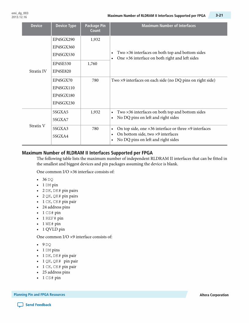
Maximum Number of RLDRAM II Interfaces Supported per FPGAThe following table lists the maximum number of independent RLDRAM II interfaces that can be fitted inthe smallest and biggest devices and pin packages assuming the device is blank.
One common I/O ×36 interface consists of:
• 36 DQ• 1 DM pin• 2 DK, DK# pin pairs• 2 QK, QK# pin pairs• 1 CK, CK# pin pair• 24 address pins• 1 CS# pin• 1 REF# pin• 1 WE# pin• 1 QVLD pin
One common I/O ×9 interface consists of:
• 9 DQ• 1 DM pins• 1 DK, DK# pin pair• 1 QK, QK# pin pair• 1 CK, CK# pin pair• 25 address pins• 1 CS# pin
Altera CorporationPlanning Pin and FPGA Resources
Send Feedback
3-21Maximum Number of RLDRAM II Interfaces Supported per FPGAemi_dg_0032013.12.16

• 1 REF# pin• 1 WE# pin• 1 QVLD pin
Table 3-8: Maximum Number of RLDRAM II Interfaces Supported per FPGA
Maximum Number of RLDRAM II CIO InterfacesPackage PinCount
Device TypeDevice
Two ×36 interfaces on each sideF1,517EP2AGZ300
EP2AGZ350
EP2AGZ225Arria II GZ• Three ×9 interfaces or one ×36 interface on both top and
bottom sides• No DQ pins on the left and right sides
F780EP2AGZ300
EP2AGZ350
• Two ×36 interfaces on both top and bottom sides• No DQ pins on left and right sides
1,5175AGXB1
5AGXB3
5AGXB5
5AGXB7
5AGTD3
5AGTD7Arria V
• One ×36 interface on both top and bottom sides• One ×18 interface on the right side• No DQ pins on the left side
6725AGXA1
5AGXA3
• One ×36 interface on both top and bottom sides• No DQ pins on the left side
6725AGXA5
5AGXA7
• Four ×36 interfaces on both top and bottom sides• No DQ pins on left and right sides
1,5175ZGZE5
5ZGZE7Arria V GZ • On top side, three ×9 interfaces or two ×36 interfaces
• On bottom side, two ×9 interfaces or one ×36 interfaces• No DQ pins on left and right sides
7805AGZE1
5AGZE3
• Four ×36 components on both top and bottom sides• Three ×36 interfaces on both right and left sides
1,760EP3SL340
Stratix III One ×9 interface on both right and left sides484EP3SE50
EP3SL50
EP3SL70
Planning Pin and FPGA ResourcesAltera Corporation
Send Feedback
emi_dg_003Maximum Number of RLDRAM II Interfaces Supported per FPGA3-22 2013.12.16

Maximum Number of RLDRAM II CIO InterfacesPackage PinCount
Device TypeDevice
• Three ×36 interfaces on both top and bottom sides• Two ×36 interfaces on both right and left sides
1,932EP4SGX290
EP4SGX360
EP4SGX530
Stratix IV
• Three ×36 interfaces on each side1,760EP4SE530
EP4SE820
One ×36 interface on each side (no DQ pins on right side)780EP4SGX70
EP4SGX110
EP4SGX180
EP4SGX230
• Four ×36 interfaces on both top and bottom sides• No DQ pins on left and right sides
1,9325SGXA5
5SGXA7Stratix V • On top side, two ×9 interfaces or one ×18 interfaces
• On bottom side, three ×9 interfaces or two ×36 interfaces• No DQ pins on left and right sides
7805SGXA3
5SGXA4
Maximum Number of LPDDR2 SDRAM Interfaces Supported per FPGAThe following table lists the maximum number of x8 LPDDR2 SDRAM components that can fit in thesmallest and largest devices and pin packages, assuming the device is blank.
Each interface of size n, where n is a multiple of 8, consists of:
• n DQ pins (including ECC)• n/8 DM pins• n/8 DQS, DQSn pin pairs• 10 address pins• 2 command pins (CKE and CSn)• 1 CK, CK# pin pair up to every three x8 LPDDR2 components
Altera CorporationPlanning Pin and FPGA Resources
Send Feedback
3-23Maximum Number of LPDDR2 SDRAM Interfaces Supported per FPGAemi_dg_0032013.12.16

Table 3-9: Maximum Number of LPDDR2 SDRAM Interfaces Supported per FPGA
Maximum Number of RLDRAM II CIO InterfacesPackage PinCount
Device TypeDevice
• One ×72 interface on both top and bottom sides• No DQ pins on the left and right sides
1,5175AGXB1
5AGXB3
5AGXB5
5AGXB7
5AGTD3
5AGTD7Arria V
• One ×64 interface or two ×24 interfaces on both top andbottom sides
• One ×32 interface on the right side
6725AGXA1
5AGXA3
• One ×64 interface or two ×24 interfaces on both the topand bottom sides
• No DQ pins on the left side
6725AGXA5
5AGXA7
• One ×72 interface or two ×32 interfaces on each of the top,bottom, and right sides
• No DQ pins on the left side
1,1525CGTD9
5CEA9
5CGXC9Cyclone V
• One ×48 interface or two ×16 interfaces on both the topand bottom sides
• One ×8 interface on the right side• No DQ pins on the left side
4845CEA7
5CGTD7
5CGXC7
OCT Support for Arria II GX, Arria II GZ, Arria V, Arria V GZ, Cyclone V, Stratix III,Stratix IV, and Stratix V Devices
If the memory interface uses any FPGA OCT calibrated series, parallel, or dynamic termination for any I/Oin your design, you need a calibration block for the OCT circuitry. This calibration block is not required tobe within the same bank or side of the device as the memory interface pins. However, the block requires apair of RUP and RDN or RZQ pins that must be placed within an I/O bank that has the same VCCIO voltageas the VCCIO voltage of the I/O pins that use the OCT calibration block.
The RZQ pin in Stratix V, Arria V, and Cyclone V devices is a dual functional pin that can also be used as DQand DQS pins when it is not used to support OCT. You can use the DQS group in ×4 mode with non-differential DQS pins if the RZQ pin is part of a ×4 DQS group.
Planning Pin and FPGA ResourcesAltera Corporation
Send Feedback
emi_dg_003OCT Support for Arria II GX, Arria II GZ, Arria V, Arria V GZ, Cyclone V, Stratix III, Stratix IV, and Stratix V Devices3-24 2013.12.16

The RUP and RDN pins in Arria II GX, Arria II GZ, Stratix III, and Stratix IV devices are dual functional pinsthat can also be used as DQ and DQS pins in when they are not used to support OCT, giving the followingimpacts on your DQS groups:
• If the RUP and RDN pins are part of a ×4 DQS group, you cannot use that DQS group in ×4 mode.• If the RUP and RDN pins are part of a ×8 DQS group, you can only use this group in ×8 mode if any of the
following conditions apply:
• You are not using DM or BWSn pins.• You are not using a ×8 or ×9 QDR II and QDR II+ SRAM devices, as the RUP and RDN pins may have
dual purpose function as the CQn pins. In this case, pick different pin locations for RUP and RDN pins,to avoid conflict with memory interface pin placement. You have the choice of placing the RUP andRDN pins in the same bank as the write data pin group or address and command pin group.
• You are not using complementary or differential DQS pins.
The QDR II and QDR II+ SRAM controller with UniPHY do not support ×8 QDR II and QDR II+SRAM devices in the Quartus II software.
Note:
A DQS/DQ ×8/×9 group in Arria II GZ, Stratix III, and Stratix IV devices comprises 12 pins. A typical ×8memory interface consists of one DQS, one DM, and eight DQ pins which add up to 10 pins. If you chooseyour pin assignment carefully, you can use the two extra pins for RUP and RDN. However, if you are usingdifferential DQS, you do not have enough pins for RUP and RDN as you only have one pin leftover. In thiscase, as you do not have to put the OCT calibration block with the DQS or DQ pins, you can pick differentlocations for the RUP and RDN pins. As an example, you can place it in the I/O bank that contains the addressand command pins, as this I/O bank has the same VCCIO voltage as the I/O bank containing the DQS andDQ pins.
There is no restriction when using ×16/×18 or ×32/×36 DQS groups that include the ×4 groups when pinmembers are used as RUP and RDN pins, as there are enough extra pins that can be used as DQS or DQ pins.
You must pick your DQS and DQ pins manually for the ×8, ×9, ×16 and ×18, or ×32 and ×36 groups, if theyare using RUP and RDN pins within the group. The Quartus II software might not place these pins optimallyand might be unable to fit the design.
General Pin-out GuidelinesAltera recommends that you place all the pins for one memory interface (attached to one controller) on thesame side of the device. For projects where I/O availability is a challenge and therefore it is necessary spreadthe interface on two sides, for optimal performance, place all the input pins on one side, and the output pinson an adjacent side of the device along with their corresponding source-synchronous clock.
For a unidirectional data bus as in QDR II and QDR II+ SRAM interfaces, do not split a read datapin group or a write data pin group onto two sides. You should also not split the address and command
Note:
group onto two sides either, especially when you are interfacing with QDR II and QDR II+ SRAMburst-length-of-two devices, where the address signals are double data rate. Failure to adhere to theserules might result in timing failure.
Altera CorporationPlanning Pin and FPGA Resources
Send Feedback
3-25General Pin-out Guidelinesemi_dg_0032013.12.16

In addition, there are some exceptions for the following interfaces:
• ×36 emulated QDR II and QDR II+ SRAM in Arria II, Stratix III, and Stratix IV devices.• RLDRAM II and RLDRAM 3 CIO devices.• QDR II/+ SDRAM burst-length-of-two devices.• You must compile the design in the Quartus II software to ensure that you are not violating signal integrity
and Quartus II placement rules, which is critical when you have transceivers in the same design.
The following are general guidelines for placing pins optimally for your memory interfaces:
1. For Arria II GZ, Arria V, Cyclone V, Stratix III, Stratix IV, and Stratix V designs, if you are using OCT,the RUP and RDN, or RZQ pins must be in any bank with the same I/O voltage as your memory interfacesignals and often use two DQS and DQ pins from a group. If you decide to place the RUP and RDN, orRZQ pins in a bank where the DQS and DQ groups are used, place these pins first and then determinehow many DQ pins you have left, to find out if your data pins can fit in the remaining pins. Refer to OCTSupport for Arria II GX, Arria II GZ, Arria V, Arria V GZ, Cyclone V, Stratix III, Stratix IV, and Stratix VDevices.
2. Use the PLL that is on the same side of the memory interface. If the interface is spread out on two adjacentsides, you may use the PLL that is located on either adjacent side. You must use the dedicated input clockpin to that particular PLL as the reference clock for the PLL as the input of the memory interface PLLcannot come from the FPGA clock network.
3. The Altera IP uses the output of the memory interface PLL for the DLL input reference clock. Therefore,ensure you select a PLL that can directly feed a suitable DLL.
Alternatively, you can use an external pin to feed into the DLL input reference clock. The availablepins are also listed in the External Memory Interfaces chapter of the relevant device family
Note:
handbook. You can also activate an unused PLL clock outputs, set it at the desired DLL frequency,and route it to a PLL dedicated output pin. Connect a trace on the PCB from this output pin tothe DLL reference clock pin, but be sure to include any signal integrity requirements such asterminations.
4. Read data pins require the usage of DQS and DQ group pins to have access to the DLL control signals.
In addition, QVLD pins in RLDRAM II and RLDRAM 3, and QDR II+ SRAM must use DQSgroup pins, when the design uses the QVLD signal. None of the Altera IP uses QVLD pins as part
Note:
of read capture, so theoretically you do not need to connect the QVLD pins if you are using theAltera solution. It is good to connect it anyway in case the Altera solution gets updated to useQVLD pins.
5. In differential clocking (DDR3/DDR2 SDRAM, RLDRAM II, and RLDRAM 3 interfaces), connect thepositive leg of the read strobe or clock to a DQS pin, and the negative leg of the read strobe or clock to aDQSn pin. For QDR II or QDR II+ SRAM devices with 2.5 or 1.5 cycles of read latency, connect the CQpin to a DQS pin, and the CQn pin to a CQn pin (and not the DQSn pin). For QDR II or QDR II+ SRAMdevices with 2.0 cycles of read latency, connect the CQ pin to a CQn pin, and the CQn pin to a DQS pin.
6. Write data (if unidirectional) and data mask pins (DM or BWSn) pins must use DQS groups. While theDLL phase shift is not used, using DQS groups for write data minimizes skew, and must use the SW andTCCS timing analysis methodology.
7. Assign the write data strobe or write data clock (if unidirectional) in the corresponding DQS/DQSn pinwith the write data groups that place in DQ pins (except in RLDRAM II and RLDRAM 3 CIO devices,refer to the Pin-out Rule Exceptions for your memory interface protocol.
Planning Pin and FPGA ResourcesAltera Corporation
Send Feedback
emi_dg_003General Pin-out Guidelines3-26 2013.12.16

Note: When interfacing with a DDR, or DDR2, or DDR3 SDRAM without leveling, put the three CKand CK# pairs in a single ×4 DQS group to minimize skew between clocks and maximize marginfor the tDQSS, tDSS, and tDSH specifications from the memory devices.
8. Assign any address pins to any user I/O pin. To minimize skew within the address pin group, you shouldassign the address and command pins in the same bank or side of the device.
9. Assign the command pins to any I/O pins and assign the pins in the same bank or device side as the othermemory interface pins, especially address and memory clock pins. The memory device usually uses thesame clock to register address and command signals.
• In QDR II and QDR II+ SRAM interfaces where the memory clock also registers the write data, assignthe address and command pins in the same I/O bank or same side as the write data pins, to minimizeskew.
• For more information about assigning memory clock pins for different device families and memorystandards, refer to Pin Connection Guidelines Tables.
Related Information
• Pin Connection Guidelines Tables on page 3-36
• Additional Guidelines for Arria V GZ and Stratix V Devices on page 3-42
• OCT Support for Arria II GX, Arria II GZ, Arria V, Arria V GZ, Cyclone V, Stratix III, Stratix IV,and Stratix V Devices on page 3-24
• Pin-out Rule Exceptions for ×36 Emulated QDR II and QDR II+ SRAM Interfaces in Arria II,Stratix III and Stratix IV Devices on page 3-28
• Pin-out Rule Exceptions for QDR II and QDR II+ SRAM Burst-length-of-two Interfaces on page3-35
• Pin-out Rule Exceptions for RLDRAM II and RLDRAM 3 Interfaces on page 3-33
Arria 10 Pin Placement Rules and GuidelinesYou must follow specific rules and guidelines when performing pin placement.
The Arria 10 I/O subsystem is located in the I/O columns. The device has up to two I/O columns that canbe used by memory interfaces. Each column consists of multiple I/O banks. Each bank consists of four I/Olanes. A lane is a group of 12 I/Os.
The following topics describe pin placement rules and guidelines.
Arria 10 Pin Placement Rules and Guidelines: Interface-LevelObserve the following rules and guidelines for interface-level pin placement.
1. The pins of a single memory interface must reside within a single I/O column.2. A memory interface can occupy one or more banks. When an interface must occupy multiple banks,
those banks must be adjacent to one another.3. Any pin that is not used by an external memory interface is available for use as a general purpose I/O of
compatible voltage and termination settings.
Altera CorporationPlanning Pin and FPGA Resources
Send Feedback
3-27Arria 10 Pin Placement Rules and Guidelinesemi_dg_0032013.12.16

Arria 10 Pin Placement Rules and Guidelines: Address/Command PinsObserve the following rules and guidelines for address and command pin placement.
1. All address/command pins for a memory interface must reside within a single bank. This bank is denotedas the address/command bank.
2. You should select the center bank of the interface as the address/command bank, to minimize latency.3. Address and command pins within the address/command bank must follow a fixed pinout scheme, as
defined in the <variation_name>_readme.txt file which is generated with your IP. The pinout schemevaries according to the topology of the memory interface. The pinout scheme is a hardware requirementthat you must follow. Some schemes require three lanes to implement address and command pins, whileothers require four lanes.
4. You do not need to specify the location of every address and command pin manually. If you assign thelocation for one address and command pin, the Fitter will automatically place the remaining address andcommand pins.
5. An unused I/O lane in the address and command bank can serve to implement a data group, such as ax8 DQS group.
6. A lane must not be used by both address and command pins and data pins.
Arria 10 Pin Placement Rules and Guidelines: Data PinsObserve the following rules and guidelines for data pin placement.
1. You must place read data groups according to the DQS/CQ/QK grouping in the pin table. Read datastrobes and clocks must reside at physical pins capable of functioning as DQS/CK/QK for a specific readdata group size. The associated data pins must be placed within the same group.
2. For protocols and topologies where a write data group consists of multiple read data groups, you shouldplace the read data groups in the same bank to improve I/O timing.
3. You do not need to specify the location of every data pin manually. If you assign the location for the readcapture strobe/clock pin pairs, the Fitter will automatically place the remaining data pins.
Arria 10 Pin Placement Rules and Guidelines: Other PinsObserve the following rules and guidelines for other pin placement.
1. PLL reference clock pins, if applicable, must be placed inside the address and command bank. Consultthe <variation_name>_readme.txt file generated with your IP for the relative location of the PLL referenceclock pin (or pin pair) within the bank.
2. RZQ pin, if applicable, must be placed inside the address and command bank. Consult the<variation_name>_readme.txt file generated with your IP for the relative location of the RZQ pin withinthe bank.
Pin-out Rule Exceptions for ×36 Emulated QDR II and QDR II+ SRAM Interfacesin Arria II, Stratix III and Stratix IV Devices
A few packages in the Arria II, Arria v GZ, Stratix III, Stratix IV, and Stratix V device families do not offerany ×32/×36 DQS groups where one read clock or strobe is associated with 32 or 36 read data pins. Thislimitation exists in the following I/O banks:
Planning Pin and FPGA ResourcesAltera Corporation
Send Feedback
emi_dg_003Arria 10 Pin Placement Rules and Guidelines: Address/Command Pins3-28 2013.12.16

• All I/O banks in U358- and F572-pin packages for all Arria II GX devices• All I/O banks in F484-pin packages for all Stratix III devices• All I/O banks in F780-pin packages for all Arria II GZ, Stratix III, and Stratix IV devices; top and side
I/O banks in F780-pin packages for all Stratix V and Arria V GZ devices• All I/O banks in F1152-pin packages for all Arria II GZ, Stratix III, and Stratix IV devices, except
EP4SGX290, EP4SGX360, EP4SGX530, EPAGZ300, and EPAGZ350 devices• Side I/O banks in F1517- and F1760-pin packages for all Stratix III devices• All I/O banks in F1517-pin for EP4SGX180, EP4SGX230, EP4S40G2, EP4S40G5, EP4S100G2, EP4S100G5,
and EPAGZ225 devices• Side I/O banks in F1517-, F1760-, and F1932-pin packages for all Arria II GZ and Stratix IV devices
This limitation limits support for ×36 QDR II and QDR II+ SRAM devices. To support these memory devices,this following section describes how you can emulate the ×32/×36 DQS groups for these devices.
• The maximum frequency supported in ×36 QDR II and QDR II+ SRAM interfaces using ×36 emulationis lower than the maximum frequency when using a native ×36 DQS group.
The F484-pin package in Stratix III devices cannot support ×32/×36 DQS group emulation, as it doesnot support ×16/×18 DQS groups.
Note:
To emulate a ×32/×36 DQS group, combine two ×16/×18 DQS groups together. For ×36 QDR II and QDRII+ SRAM interfaces, the 36-bit wide read data bus uses two ×16/×18 groups; the 36-bit wide write data usesanother two ×16/×18 groups or four ×8/×9 groups. The CQ and CQn signals from the QDR II and QDRII+ SRAM device traces are then split on the board to connect to two pairs of CQ/CQn pins in the FPGA.You might then need to split the QVLD pins also (if you are connecting them). These connections are theonly connections on the board that you need to change for this implementation. There is still only one pairof K and Kn# connections on the board from the FPGA to the memory (see the following figure). Use anexternal termination for the CQ/CQn signals at the FPGA end. You can use the FPGA OCT features on theother QDR II interface signals with ×36 emulation. In addition, there may be extra assignments to be addedwith ×36 emulation.
Other QDR II and QDR II+ SRAM interface rules also apply for this implementation.Note:
You may also combine four ×9 DQS groups (or two ×9 DQS groups and one ×18 group) on the same sideof the device, if not the same I/O bank, to emulate a x36 write data group, if you need to fit the QDR IIinterface in a particular side of the device that does not have enough ×18 DQS groups available for writedata pins. Altera does not recommend using ×4 groups as the skew may be too large, as you need eight ×4groups to emulate the ×36 write data bits.
You cannot combine four ×9 groups to create a ×36 read data group as the loading on the CQ pin is toolarge and hence the signal is degraded too much.
When splitting the CQ and CQn signals, the two trace lengths that go to the FPGA pins must be as short aspossible to reduce reflection. These traces must also have the same trace delay from the FPGA pin to the Yor T junction on the board. The total trace delay from the memory device to each pin on the FPGA shouldmatch the Q trace delay (I2).
You must match the trace delays. However, matching trace length is only an approximation tomatching actual delay.
Note:
Altera CorporationPlanning Pin and FPGA Resources
Send Feedback
3-29Pin-out Rule Exceptions for ×36 Emulated QDR II and QDR II+ SRAM Interfaces in Arria II, Stratix III and Stratix IVDevices
emi_dg_0032013.12.16

Figure 3-7: Board Trace Connection for Emulated x36 QDR II and QDR II+ SRAM Interface
DDR
DDR
DDR
DDR
FPGA IOE
length = l1
length = l1
length = l1
length = l2
DDRD, A
Q
K
Kn
CQlength = l2 CQnlength = l2DQS Logic
Block
enaLatch
QDR IISRAM
DQS
DQSn
DQ (18-bit)
DDR
DDR
length = l2Q
enaLatch
DQ (18-bit)
Timing Impact on x36 EmulationWith ×36 emulation, the CQ/CQn signals are split on the board, so these signals see two loads (to the twoFPGA pins)—the DQ signals still only have one load. The difference in loading gives some slew ratedegradation, and a later CQ/CQn arrival time at the FPGA pin.
The slew rate degradation factor is taken into account during timing analysis when you indicate in theUniPHY Preset Editor that you are using ×36 emulation mode. However, you must determine the differencein CQ/CQn arrival time as it is highly dependent on your board topology.
The slew rate degradation factor for ×36 emulation assumes that CQ/CQn has a slower slew rate than aregular ×36 interface. The slew rate degradation is assumed not to be more than 500 ps (from 10% to 90%
Planning Pin and FPGA ResourcesAltera Corporation
Send Feedback
emi_dg_003Timing Impact on x36 Emulation3-30 2013.12.16
VCCIO swing). You may also modify your board termination resistor to improve the slew rate of the ×36-emulated CQ/CQn signals. If your modified board does not have any slew rate degradation, you do not needto enable the ×36 emulation timing in the UniPHY-based controller MegaWizard™ interface.
For more information about how to determine the CQ/CQn arrival time skew, refer to Determining theCQ/CQn Arrival Time Skew.
Because of this effect, the maximum frequency supported using x36 emulation is lower than the maximumfrequency supported using a native x36 DQS group.
Related InformationDetermining the CQ/CQn Arrival Time Skew on page 3-31
Rules to Combine GroupsFor devices that do not have four ×16/×18 groups in a single side of the device to form two ×36 groups forread and write data, you can form one ×36 group on one side of the device, and another ×36 group on theother side of the device. All the read groups have to be on the same edge (column I/O or row I/O) and allwrite groups have to be on the same type of edge (column I/O or row I/O), so you can have an interface withthe read group in column I/O and the write group in row I/O. The only restriction is that you cannot combinean ×18 group from column I/O with an ×18 group from row IO to form a x36-emulated group.
For vertical migration with the ×36 emulation implementation, check if migration is possible and enabledevice migration in the Quartus II software.
I/O bank 1C in both Stratix III and Stratix IV devices has dual-function configuration pins. Some ofthe DQS pins may not be available for memory interfaces if these are used for device configurationpurposes.
Note:
Each side of the device in these packages has four remaining ×8/×9 groups. You can combine four of theremaining for the write side (only) if you want to keep the ×36 QDR II and QDR II+ SRAM interface onone side of the device, by changing the Memory Interface Data Group default assignment, from the default18 to 9.
For more information about rules to combine groups for your target device, refer to the External MemoryInterfaces chapter in the respective device handbooks.
Determining the CQ/CQn Arrival Time SkewBefore compiling a design in the Quartus II software, you need to determine the CQ/CQn arrival time skewbased on your board simulation. You then need to apply this skew in the report_timing.tcl file of yourQDR II and QDR II+ SRAM interface in the Quartus II software.
The following figure shows an example of a board topology comparing an emulated case where CQ is double-loaded and a non-emulated case where CQ only has a single load.
Altera CorporationPlanning Pin and FPGA Resources
Send Feedback
3-31Rules to Combine Groupsemi_dg_0032013.12.16

Figure 3-8: Board Simulation Topology Example
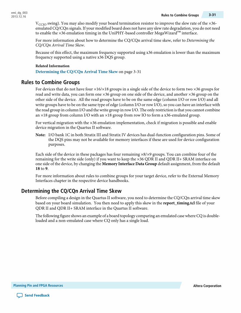
Run the simulation and look at the signal at the FPGA pin. The following figure shows an example of thesimulation results from the preceding figure. As expected, the double-loaded emulated signal, in pink, arrivesat the FPGA pin later than the single-loaded signal, in red. You then need to calculate the difference of thisarrival time at VREF level (0.75 V in this case). Record the skew and rerun the simulation in the other twocases (slow-weak and fast-strong). To pick the largest and smallest skew to be included in Quartus II timinganalysis, follow these steps:
1. Open the <variation_name>_report_timing.tcl and search fortmin_additional_dqs_variation.2. Set the minimum skew value from your board simulation totmin_additional_dqs_variation.3. Set the maximum skew value from your board simulation totmax_additional_dqs_variation.4. Save the .tcl file.
Planning Pin and FPGA ResourcesAltera Corporation
Send Feedback
emi_dg_003Determining the CQ/CQn Arrival Time Skew3-32 2013.12.16
Figure 3-9: Board Simulation Results
Pin-out Rule Exceptions for RLDRAM II and RLDRAM 3 InterfacesRLDRAM II and RLDRAM 3 CIO devices have one bidirectional bus for the data, but there are two differentsets of clocks: one for read and one for write. As the QK and QK# already occupies the DQS and DQSn pinsneeded for read, placement of DK and DK# pins are restricted due to the limited number of pins in theFPGA. This limitations causes the exceptions to the previous rules, which are discussed below.
The address or command pins of RLDRAM II must be placed in a DQ-group because these pins are drivenby the PHY clock. Half-rate RLDRAM II interfaces and full-rate RLDRAM 3 interfaces use the PHY clockfor both the DQ pins and the address or command pins.
Interfacing with ×9 RLDRAM II CIO DevicesRLDRAM 3 devices do not have the x9 configuration.
Altera CorporationPlanning Pin and FPGA Resources
Send Feedback
3-33Pin-out Rule Exceptions for RLDRAM II and RLDRAM 3 Interfacesemi_dg_0032013.12.16

RLDRAM II devices have the following pins:
• 2 pins for QK and QK# signals• 9 DQ pins (in a ×8/×9 DQS group)• 2 pins for DK and DK# signals• 1 DM pin• 14 pins total (15 if you have a QVLD)
In the FPGA, the ×8/×9 DQS group consists of 12 pins: 2 for the read clocks and 10 for the data. In this case,move the QVLD (if you want to keep this connected even though this is not used in the Altera memoryinterface solution) and the DK and DK# pins to the adjacent DQS group. If that group is in use, move toany available user I/O pins in the same I/O bank.
Interfacing with ×18 RLDRAM II and RLDRAM 3 CIO DevicesThis topic describes interfacing with x18 RLDRAM II and RLDRAM 3 devices.
RLDRAM II devices have the following pins:
• 4 pins for QK/QK# signals• 18 DQ pins (in ×8/×9 DQS group)• 2 pins for DK/DK# signals• 1 DM pin• 25 pins total (26 if you have a QVLD)
In the FPGA, you use two ×8/×9 DQS group totaling 24 pins: 4 for the read clocks and 18 for the read data.
Each ×8/×9 group has one DQ pin left over that can either use QVLD or DM, so one ×8/×9 group has theDM pin associated with that group and one ×8/×9 group has the QVLD pin associated with that group.
RLDRAM 3 devices have the following pins:
• 4 pins for QK/QK# signals• 18 DQ pins (in ×8/×9 DQS group)• 4 pins for DK/DK# signals• 2 DM pins• 28 pins total (29 if you have a QVLD)
In the FPGA, you use two ×8/×9 DQS group totaling 24 pins: 4 for the read clocks and 18 for the read data.
Each ×8/×9 group has one DQ pin left over that can either use QVLD or DM, so one ×8/×9 group has theDM pin associated with that group and one ×8/×9 group has the QVLD pin associated with that group.
Interfacing with RLDRAM II and RLDRAM 3 ×36 CIO DevicesThis topic describes interfacing with RLDRAM II and RLDRAM 3 x36 CIO devices.
RLDRAM II devices have the following pins:
• 4 pins for QK/QK# signals• 36 DQ pins (in x16/x18 DQS group)• 4 pins for DK/DK# signals• 1 DM pins• 46 pins total (47 if you have a QVLD)
Planning Pin and FPGA ResourcesAltera Corporation
Send Feedback
emi_dg_003Interfacing with ×18 RLDRAM II and RLDRAM 3 CIO Devices3-34 2013.12.16

In the FPGA, you use two ×16/×18 DQS groups totaling 48 pins: 4 for the read clocks and 36 for the readdata. Configure each ×16/×18 DQS group to have:
• Two QK/QK# pins occupying the DQS/DQSn pins• Pick two DQ pins in the ×16/×18 DQS groups that are DQS and DQSn pins in the ×4 or ×8/×9 DQS
groups for the DK and DK# pins• 18 DQ pins occupying the DQ pins• There are two DQ pins leftover that you can use for QVLD or DM pins. Put the DM pin in the group
associated with DK[1] and the QVLD pin in the group associated with DK[0].• Check that DM is associated with DK[1] for your chosen memory component.
RLDRAM 3 devices have the following pins:
• 8 pins for QK/QK# signals• 36 DQ pins (in x8/x9 DQS group)• 4 pins for DK/DK# signals• 2 DM pins• 48 pins total (49 if you have a QVLD)
In the FPGA, you use four ×8/×9 DQS groups.
In addition, observe the following placement rules for RLDRAM 3 interfaces:
For ×18 devices:
• Use two ×8/×9 DQS groups. Assign the QK/QK# pins and the DQ pins of the same read group to thesame DQS group.
• DQ, DM, and DK/DK# pins belonging to the same write group should be assigned to the same I/O sub-bank, for timing closure.
• Whenever possible, assign CK/CK# pins to the same I/O sub-bank as the DK/DK# pins, to improvetCKDK timing.
For ×36 devices:
• Use four ×8/×9 DQS groups. Assign the QK/QK# pins and the DQ pins of the same read group to thesame DQS group.
• DQ, DM, and DK/DK# pins belonging to the same write group should be assigned to the same I/O sub-bank, for timing closure.
• Whenever possible, assign CK/CK# pins to the same I/O sub-bank as the DK/DK# pins, to improvetCKDK timing.
Pin-out Rule Exceptions for QDR II and QDR II+ SRAM Burst-length-of-twoInterfaces
If you are using the QDR II and QDR II+ SRAM burst-length-of-two devices, you may want to place theaddress pins in a DQS group to minimize skew, because these pins are now double data rate too.
The address pins typically do not exceed 22 bits, so you may use one ×18 DQS groups or two ×9 DQS groupson the same side of the device, if not the same I/O bank. In Arria V GZ, Stratix III, Stratix IV, and Stratix Vdevices, one ×18 group typically has 22 DQ bits and 2 pins for DQS/DQSn pins, while one ×9 group typicallyhas 10 DQ bits with 2 pins for DQS/DQSn pins. Using ×4 DQS groups should be a last resort.
Altera CorporationPlanning Pin and FPGA Resources
Send Feedback
3-35Pin-out Rule Exceptions for QDR II and QDR II+ SRAM Burst-length-of-two Interfacesemi_dg_0032013.12.16

Pin Connection Guidelines TablesThe following table lists the FPGA pin utilization for DDR, DDR2, and DDR3 SDRAM without levelinginterfaces.
Table 3-10: FPGA Pin Utilization for DDR, DDR2, and DDR3 SDRAM without Leveling Interfaces
FPGA Pin UtilizationMemory Device Pin
NameInterface PinDescription Arria V, Cyclone V,
and Stratix VArria II GZ, Stratix III,
and Stratix IVArria II GX
If you are using single-endedDQS signaling, place anyunused DQ or DQS pins withDIFFOUT capability in thesame bank or on the sameside as the data pins.
If you are using differentialDQS signaling, place anyunused DQ or DQS pins withDIFFOUT capability for themem_clk[n:0] and mem_clk_n[n:0] signals (wheren>=0). CK pins must use thedifferential pairs where bothpins of the pair are DQ orDQS pins.
Do not place CK and CK#pins in the same group as anyother DQ or DQS pins.
If there are multiple CK andCK# pin pairs, place them onDIFFOUT in the same singleDQ group of adequate width.
If you are usingsingle-ended DQSsignaling, place anyDIFFOUTpins in thesame bank or on thesame side as the datapins
If you are usingdifferential DQSsignaling in UniPHYIP, place anyDIFFOUTpins in thesame bank or on thesame side as the datapins. If there aremultiple CK/CK#pairs, place them onDIFFOUT in thesame single DQgroup of adequatewidth.
For example, DIMMsrequiring threememory clock pin-pairs must use a ×4DQS group.
If you are usingsingle-ended DQSsignaling, place anyunused DQ or DQSpins with DIFFOUTcapability located inthe same bank or onthe same side as thedata pins.
If you are usingdifferential DQSsignaling in UniPHYIP, place onDIFFOUT in thesame single DQgroup of adequatewidth to minimizeskew.
CK and CK# (1)(2)
MemorySystemClock
Dedicated PLL clock input pin with direct connection to the PLL (not usingthe global clock network).
For Arria II GX, Arria II GZ, Arria V GZ, Stratix III, Stratix IV and StratixV Devices, also ensure that the PLL can supply the input reference clock tothe DLL. Otherwise, refer to alternative DLL input reference clocks (seeGeneral Pin-out Guidelines).
—ClockSource
Dedicated clock input pin to accommodate the high fan-out signal.—Reset
DQ in the pin table, marked as Q in the Quartus II Pin Planner. Each DQgroup has a common background color for all of the DQ and DM pins,associated with DQS (and DQSn) pins.
DQData
DMData mask
Planning Pin and FPGA ResourcesAltera Corporation
Send Feedback
emi_dg_003Pin Connection Guidelines Tables3-36 2013.12.16

FPGA Pin UtilizationMemory Device Pin
NameInterface PinDescription Arria V, Cyclone V,
and Stratix VArria II GZ, Stratix III,
and Stratix IVArria II GX
DQS (S in the Quartus II Pin Planner) for single-ended DQS signaling orDQS and DQSn (S and Sbar in the Quartus II Pin Planner) for differentialDQS signaling. DDR2 supports either single-ended or differential DQSsignaling. DDR3 SDRAM mandates differential DQS signaling.
DQS or DQS andDQSn (DDR2 andDDR2 SDRAMonly)
Data strobe
Any user I/O pin. To minimize skew, you must place the address andcommand pins in the same bank or side of the device as the CK/CK# pins,DQ, DQS, or DM pins. The reset# signal is only available in DDR3 SDRAMinterfaces. Altera devices use the SSTL-15 I/O standard on the RESET#signal to meet the voltage requirements of 1.5 V CMOS at the memorydevice. Altera recommends that you do not terminate the RESET# signalto VTT.
A[], BA[], CAS#,CKE, CS#, ODT,RAS#, WE#,RESET#
Addressandcommand
Notes to Table:
1. The first CK/CK# pair refers to mem_clk[0] or mem_clk_n[0] in the IP core.2. The restriction on the placement for the first CK/CK# pair is required because this placement allows the
mimic path that the IP VT tracking uses to go through differential I/O buffers to mimic the differentialDQS signals.
Related InformationGeneral Pin-out Guidelines on page 3-25
DDR3 SDRAM With Leveling Interface Pin Utilization Applicable for Arria V GZ, StratixIII, Stratix IV, and Stratix V Devices
The following table lists the FPGA pin utilization for DDR3 SDRAM with leveling interfaces.
Altera CorporationPlanning Pin and FPGA Resources
Send Feedback
3-37DDR3 SDRAM With Leveling Interface Pin Utilization Applicable for Arria V GZ, Stratix III, Stratix IV, and StratixV Devices
emi_dg_0032013.12.16
Table 3-11: DDR3 SDRAM With Leveling Interface Pin Utilization Applicable for Arria V GZ, Stratix III, StratixIV, and Stratix V Devices
FPGA Pin UtilizationMemory Device PinName
Interface Pin Description
DQ in the pin table, marked as Q in the Quartus II Pin Planner.Each DQ group has a common background color for all of theDQ and DM pins, associated with DQS (and DQSn) pins. The×4 DIMM has the following mapping between DQS and DQpins:
• DQS[0] maps to DQ[3:0]• DQS[9] maps to DQ[7:4]• DQS[1] maps to DQ[11:8]• DQS[10] maps to DQ[15:12]
The DQS pin index in other DIMM configurations typicallyincreases sequentially with the DQ pin index (DQS[0]:DQ[3:0]; DQS[1]: DQ[7:4]; DQS[2]: DQ[11:8]). In this DIMMconfiguration, the DQS pins are indicted this way to ensurepin out is compatible with both ×4 and ×8 DIMMs.
DQData
DMData Mask
DQS and DQSn (S and Sbar in the Quartus II Pin Planner)DQS and DQSnData Strobe
Any user I/O pin. To minimize skew, you should place addressand command pins in the same bank or side of the device asthe following pins: CK/CK# pins, DQ, DQS, or DM pins.
A[], BA[], CAS#, CKE,CS#, ODT, RAS#, WE#,
Address andCommand Altera recommends that you use the 1.5V CMOS I/O standard
on theRESET# signal. If your board is already using the SSTL-15 I/O standard, you do not terminate the RESET# signal toVTT.
RESET#
For controllers with UniPHY IP, you can assign the memoryclock to any unused DIFF_OUT pins in the same bank or onthe same side as the data pins. However, for Arria V GZ andStratix V devices, place the memory clock pins to any unusedDQ or DQS pins. Do not place the memory clock pins in thesame DQ group as any other DQ or DQS pins.
If there are multiple CK/CK# pin pairs using Arria V GZ orStratix V devices, you must place them on DIFFOUT in thesame single DQ groups of adequate width. For example,DIMMs requiring three memory clock pin-pairs must use a×4 DQS group.
Placing the multiple CK/CK# pin pairs on DIFFOUT in thesame single DQ groups for Stratix III and Stratix IV devicesimproves timing.
CK and CK#Memory systemclock
Dedicated PLL clock input pin with direct (not using a globalclock net) connection to the PLL and optional DLL requiredby the interface.
—Clock Source
Planning Pin and FPGA ResourcesAltera Corporation
Send Feedback
emi_dg_003DDR3 SDRAM With Leveling Interface Pin Utilization Applicable for Arria V GZ, Stratix III, Stratix IV, and StratixV Devices
3-38 2013.12.16
FPGA Pin UtilizationMemory Device PinName
Interface Pin Description
Dedicated clock input pin to accommodate the high fan-outsignal.
—Reset
QDR II and QDR II+ SRAM Pin Utilization for Arria II, Arria V, Stratix III, Stratix IV, andStratix V Devices
The following table lists the FPGA pin utilization for QDR II and QDR II+ SRAM interfaces.
Table 3-12: QDR II and QDR II+ SRAM Pin Utilization for Arria II, Arria V, Stratix III, Stratix IV, and Stratix VDevices
FPGA Pin UtilizationMemory Device PinName
Interface Pin Description
For QDR II SRAM devices with 1.5 or 2.5 cycles of read latencyor QDR II+ SRAM devices with 2.5 cycles of read latency,connect CQ to DQS pin (S in the Quartus II Pin Planner), andCQn to CQn pin (Qbar in the Quartus II Pin Planner).
For QDR II or QDR II+ SRAM devices with 2.0 cycles of readlatency, connect CQ to CQn pin (Qbar in the Quartus II PinPlanner), and CQn to DQS pin (S in the Quartus II PinPlanner).
Arria V devices do not use CQn. The CQ rising and fallingedges are used to clock the read data, instead of separate CQand CQn signals.
CQ and CQ# (1)Read Clock
DQ pins (Q in the Quartus II Pin Planner). Ensure that youare using the DQ pins associated with the chosen read clockpins (DQS and CQn pins). QVLD pins are only available forQDR II+ SRAM devices and note that Altera IP does not usethe QVLD pin.
QRead Data
QVLDData Valid
Differential or pseudo-differential DQ, DQS, or DQSn pinsin or near the write data group.
K and K#Memory and WriteData Clock
DQ pins. Ensure that you are using the DQ pins associatedwith the chosen memory and write data clock pins (DQS andDQS pins).
DWrite Data
BWS#, NWS#Byte Write Select
Any user I/O pin. To minimize skew, you should place addressand command pins in the same bank or side of the device asthe following pins: K and K# pins, DQ, DQS, BWS#, andNWS# pins. If you are using burst-length-of-two devices, placethe address signals in a DQS group pin as these signals arenow double data rate.
A, WPS#, RPS#Address andControl Signals
Dedicated PLL clock input pin with direct (not using a globalclock net) connection to the PLL and optional DLL requiredby the interface.
—Clock source
Altera CorporationPlanning Pin and FPGA Resources
Send Feedback
3-39QDR II and QDR II+ SRAM Pin Utilization for Arria II, Arria V, Stratix III, Stratix IV, and Stratix V Devicesemi_dg_0032013.12.16

FPGA Pin UtilizationMemory Device PinName
Interface Pin Description
Dedicated clock input pin to accommodate the high fan-outsignal
—Reset
Note to table:
1. For Arria V designs with integer latency, connect the CQ# signal to the CQ/CQ# pins from the pin tableand ignore the polarity in the Pin Planner. For Arria V designs with fractional latency, connect the CQsignal to the CQ/CQ# pins from the pin table.
RLDRAM II CIO Pin Utilization for Arria II GZ, Arria V, Stratix III, Stratix IV, and StratixV Devices
The following table lists the FPGA pin utilization for RLDRAM II CIO and RLDRAM 3 interfaces.
Table 3-13: RLDRAM II CIO Pin Utilization for Arria II GZ, Arria V, Stratix III, Stratix IV, and Stratix V Devices andRLDRAM 3 Pin Utilization for Arria V GZ and Stratix V Devices
FPGA Pin UtilizationMemory Device PinName
Interface Pin Description
DQS and DQSn pins (S and Sbar in the Quartus II Pin Planner)QK and QK# (1)Read Clock
DQ pins (Q in the Quartus II Pin Planner). Ensure that youare using the DQ pins associated with the chosen read clockpins (DQS and DQSn pins). Altera IP does not use the QVLDpin. You may leave this pin unconnected on your board. Youmay not be able to fit these pins in a DQS group. For moreinformation about how to place these pins, refer to “Exceptionsfor RLDRAM II and RLDRAM 3 Interfaces” on page 3–34.
QData
QVLDData Valid
DMData Mask
DQ pins in the same DQS group as the read data (Q) pins orin adjacent DQS group or in the same bank as the address andcommand pins. For more information, refer to “Exceptionsfor RLDRAM II and RLDRAM 3 Interfaces” on page 3–34.DK/DK# must use differential output-capable pins.
For Nios-based configuration, the DK pins must be in a DQgroup but the DK pins do not have to be in the same group asthe data or QK pins.
DK and DK#Write Data Clock
Any differential output-capable pins.
For Arria V GZ and Stratix V devices, place any unused DQor DQS pins with DIFFOUT capability. Place the memoryclock pins either in the same bank as the DK or DK# pins toimprove DK versus CK timing, or in the same bank as theaddress and command pins to improve address commandtiming. Do not place CK and CK# pins in the same DQ groupas any other DQ or DQS pins.
CK and CK#Memory Clock
Planning Pin and FPGA ResourcesAltera Corporation
Send Feedback
emi_dg_003RLDRAM II CIO Pin Utilization for Arria II GZ, Arria V, Stratix III, Stratix IV, and Stratix V Devices3-40 2013.12.16

FPGA Pin UtilizationMemory Device PinName
Interface Pin Description
Any user I/O pins. To minimize skew, you should placeaddress and command pins in the same bank or side of thedevice as the following pins: CK/CK# pins, DQ, DQS, and DMpins.
A, BA, CS#, REF#, WE#Address andControl Signals
Dedicated PLL clock input pin with direct (not using a globalclock net) connection to the PLL and optional DLL requiredby the interface.
—Clock source
Dedicated clock input pin to accommodate the high fan-outsignal
—Reset
Note to Table:
1. For Arria V devices, refer to the pin table for the QK and QK# pins. Connect QK and QK# signals to theQK and QK# pins from the pin table and ignore the polarity in the Pin Planner.
Related InformationPin-out Rule Exceptions for RLDRAM II and RLDRAM 3 Interfaces on page 3-33
LPDDR2 Pin Utilization for Arria V, Cyclone V, and Stratix V DevicesThe following table lists the FPGA pin utilization for LPDDR2 SDRAM.
Table 3-14: LPDDR2 Pin Utilization for Arria V, Cyclone V, and Stratix V Devices
FPGA Pin UtilizationMemory Device PinName
Interface Pin Description
Differential clock inputs. All double data rate (DDR) inputsare sampled on both positive and negative edges of the CKsignal. Single data rate (SDR) inputs are sampled at the positiveclock edge. Place any unused DQ or DQS pins with DIFFOUTcapability for the mem_clk[n:0] and mem_clk_n[n:0] signals(where n>=0). Do not place CK and CK# pins in the samegroup as any other DQ or DQS pins. If there are multiple CKand CK# pin pairs, place them on DIFFOUT in the same singleDQ group of adequate width.
CK, CKnMemory Clock
Unidirectional DDR command and address bus inputs. ChipSelect: CSn is considered to be part of the commandcode.Clock Enable: CKE HIGH activates and CKE LOWdeactivates internal clock signals and therefore device inputbuffers and output drivers. Place address and command pinsin any DDR-capable I/O pin. To minimize skew, Alterarecommends using address and command pins in the samebank or side of the device as the CK/CK#, DQ. DQS, or DMpins..
CA0-CA9
CSn
CKE
Address andCommand
Altera CorporationPlanning Pin and FPGA Resources
Send Feedback
3-41LPDDR2 Pin Utilization for Arria V, Cyclone V, and Stratix V Devicesemi_dg_0032013.12.16

FPGA Pin UtilizationMemory Device PinName
Interface Pin Description
Bidirectional data bus. Pins are used as data inputs andoutputs. DQ in the pin table is marked as Q in the Pin Planner.Each DQ group has a common background color for all of theDQ and DM pins associated with DQS (and DQSn) pins. Placeon DQ group pin marked Q in the Pin Planner.
DQ0-DQ7 (×8)
DQ0-DQ15 (×16)
DQ0-DQ31 (×32)
Data
Data Strobe. The data strobe is bidirectional (used for readand write data) and differential (DQS and DQSn). It is outputwith read data and input with write data. Place on DQS andDQSn (S and Sbar in the Pin Planner) for differential DQSsignaling.
DQS, DQSnData Strobe
Input Data Mask. DM is the input mask signal for write data.Input data is masked when DM is sampled HIGH coincidentwith that input data during a write access. DM is sampled onboth edges of DQS. DQ in the pin table is marked as Q in thePin Planner. Each DQ group has a common background colorfor all of the DQ and DM pins, associated with DQS (andDQSn) pins. Place on DQ group pin marked Q in the PinPlanner.
DM0 (×8)
DM0-DM1 (×16)
DM0-DM3 (×32)
Data Mask
Dedicated PLL clock input pin with direct (not using a globalclock net) connection to the PLL and optional DLL requiredby the interface.
—Clock Source
Dedicated clock input pin to accommodate the high fan-outsignal.
—Reset
Additional Guidelines for Arria V GZ and Stratix V DevicesThis section provides guidelines for improving timing for Arria V GZ and Stratix V devices and the rulesthat you must follow to overcome timing failures.
Performing Manual Pin Placement
The following table lists rules that you can follow to perform proper manual pin placement and avoid timingfailures.
The rules are categorized as follows:
• Mandatory—This rule is mandatory and cannot be violated as it would result in a no-fit error.• Recommended—This rule is recommended and if violated the implementation is legal but the timing is
degraded.• Highly Recommended—This rule is not mandatory but is highly recommended because disregarding
this rule might result in timing violations.
Table 3-15: Manual Pin Placement Rules
ReasonDeviceFrequencyRules
Mandatory
Planning Pin and FPGA ResourcesAltera Corporation
Send Feedback
emi_dg_003Additional Guidelines for Arria V GZ and Stratix V Devices3-42 2013.12.16
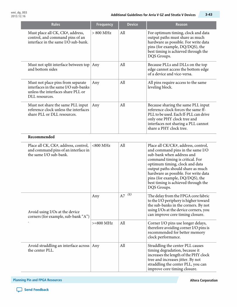
ReasonDeviceFrequencyRules
For optimum timing, clock and dataoutput paths must share as muchhardware as possible. For write datapins (for example, DQ/DQS), thebest timing is achieved through theDQS Groups.
All> 800 MHzMust place all CK, CK#, address,control, and command pins of aninterface in the same I/O sub-bank.
Because PLLs and DLLs on the topedge cannot access the bottom edgeof a device and vice-versa.
AllAnyMust not split interface between topand bottom sides
All pins require access to the sameleveling block.
AllAnyMust not place pins from separateinterfaces in the same I/O sub-banksunless the interfaces share PLL orDLL resources.
Because sharing the same PLL inputreference clock forces the same ff-PLL to be used. Each ff-PLL can driveonly one PHY clock tree andinterfaces not sharing a PLL cannotshare a PHY clock tree.
AllAnyMust not share the same PLL inputreference clock unless the interfacesshare PLL or DLL resources.
Recommended
Place all CK/CK#, address, control,and command pins in the same I/Osub-bank when address andcommand timing is critical. Foroptimum timing, clock and dataoutput paths should share as muchhardware as possible. For write datapins (for example, DQ/DQS), thebest timing is achieved through theDQS Groups.
All<800 MHzPlace all CK, CK#, address, control,and command pins of an interface inthe same I/O sub-bank.
The delay from the FPGA core fabricto the I/O periphery is higher towardthe sub-banks in the corners. By notusing I/Os at the device corners, youcan improve core timing closure.
A7 (1)Any
Avoid using I/Os at the devicecorners (for example, sub-bank “A”). Corner I/O pins use longer delays,
therefore avoiding corner I/O pins isrecommended for better memoryclock performance.
All>=800 MHz
Straddling the center PLL causestiming degradation, because itincreases the length of the PHY clocktree and increases jitter. By notstraddling the center PLL, you canimprove core timing closure.
AllAnyAvoid straddling an interface acrossthe center PLL.
Altera CorporationPlanning Pin and FPGA Resources
Send Feedback
3-43Additional Guidelines for Arria V GZ and Stratix V Devicesemi_dg_0032013.12.16

ReasonDeviceFrequencyRules
Using a non-center PLL results indriving a sub-bank in the oppositequadrant due to long PHY clock treedelay.
All>= 800 MHzUse the center PLL(f-PLL1) for awide interface that must straddleacross center PLL.
To ease core timing closure. If thepins are too far apart then the corelogic is also placed apart whichresults in difficult timing closure.
AllAnyPlace the DQS/DQS# pins such thatall DQ groups of the same interfaceare next to each other and do notspan across the center PLL.
AllAnyPlace CK, CK#, address, control, andcommand pins in the same quadrantas DQ groups for improved timingin general.
Highly Recommended
For optimum timing, clock and dataoutput paths should share as muchhardware as possible. For write datapins (for example, DQ/DQS), thebest timing is achieved through theDQS Groups.
All800 MHzPlace all CK, CK#, address, control,and command pins of an interface inthe same I/O sub-bank.
Using a non-center PLL results indriving a sub-bank in the oppositequadrant due to long PHY clock treedelay.
All>= 800 MHzUse center PLL and ensure that thePLL input reference clock pin isplaced at a location that can drive thecenter PLL.
All>= 800 MHzIf center PLL is not accessible, placepins in the same quadrant as the PLL.
Note to Table:
1. This rule is currently applicable to A7 devices only. This rule might be applied to other devices in thefuture if they show the same failure.
Additional Guidelines for Arria V ( Except Arria V GZ) DevicesThis section provides guidelines on how to improve timing for Arria V devices and the rules that you mustfollow to overcome timing failures.
Performing Manual Pin Placement
The following table lists rules you can follow to perform proper manual pin placement and avoid timingfailures.
The rules are categorized as follows:
• Mandatory—This rule is mandatory and cannot be violated as it would result in a no-fit error.• Recommended—This rule is recommended and if violated the implementation is legal but the timing is
degraded.
Planning Pin and FPGA ResourcesAltera Corporation
Send Feedback
emi_dg_003Additional Guidelines for Arria V ( Except Arria V GZ) Devices3-44 2013.12.16
Table 3-16: Manual Pin Placement Rules for Arria V (Except Arria V GZ) Devices
ReasonDeviceFrequencyRules
Mandatory
For optimum timing, clock anddata output ports must share asmuch hardware as possible.
AllAllMust place all CK, CK#, address,control, and command pins of aninterface on the same device edgeas the DQ groups.
All pins require access to the samePLL/DLL block.
AllAllMust not place pins from separateinterfaces in the same I/O sub-banks unless the interfaces sharePLL or DLL resources. To shareresources, the interfaces must usethe same memory protocol,frequency, controller rate, andphase requirements.
PHYCLK network supportinterfaces at the same side of the I/O banks only. PHYCLK networksdo not support split interface.
AllAllMust not split interface betweentop, bottom, and right sides.
Recommended
To ease core timing closure. If thepins are too far apart then the corelogic is also placed apart whichresults in difficult timing closure.
AllAllPlace the DQS/DQS# pins such thatall DQ groups of the same interfaceare next to each other and do notspan across the center PLL.
Improve timing performance byreducing the PHY clock tree delay.
AllAllPlace all pins for a memoryinterface in an I/O bank and use thenearest PLL to that I/O bank for thememory interface.
Additional Guidelines for Cyclone V DevicesThis topic provides guidelines for improving performance for Cyclone V devices.
I/O Pins Connect to Ground for Hard Memory Interface Operation
According to the Cyclone V pin-out file, there are some general I/O pins that are connected to ground forhard memory interface operation. These I/O pins should be grounded to reduce crosstalk from neighboringI/O pins and to ensure the performance of the hard memory interface.
The grounded user I/O pins can also be used as regular I/O pins if you run short of available I/O pins;however, the hard memory interface performance will be reduced if these pins are not connected to ground.
PLLs and Clock NetworksThe exact number of clocks and PLLs required in your design depends greatly on the memory interfacefrequency, and on the IP that your design uses.
Altera CorporationPlanning Pin and FPGA Resources
Send Feedback
3-45Additional Guidelines for Cyclone V Devicesemi_dg_0032013.12.16

For example, you can build simple DDR slow-speed interfaces that typically require only two clocks: systemand write. You can then use the rising and falling edges of these two clocks to derive four phases (0°, 90°,180°, and 270°). However, as clock speeds increase, the timing margin decreases and additional clocks arerequired, to optimize setup and hold and meet timing. Typically, at higher clock speeds, you need to havededicated clocks for resynchronization, and address and command paths.
Altera memory interface IP uses one PLL, which generates the various clocks needed in the memory interfacedata path and controller, and provides the required phase shifts for the write clock and address and commandclock. The PLL is instantiated when you generate the Altera memory IPs.
By default, the memory interface IP uses the PLL to generate the input reference clock for the DLL, availablein all supported device families. This method eliminates the need of an extra pin for the DLL input referenceclock.
The input reference clock to the DLL can come from certain input clock pins or clock output from certainPLLs.
Altera recommends using integer PLLs for memory interfaces; handbook specifications are basedon integer PLL implementations.
Note:
For the actual pins and PLLs connected to the DLLs, refer to the External Memory Interfaces chapter of therelevant device family handbook.
You must use the PLL located in the same device quadrant or side as the memory interface and thecorresponding dedicated clock input pin for that PLL, to ensure optimal performance and accurate timingresults from the Quartus II software.
The input clock to the PLL can fan out to logic other than the PHY, so long as the clock input pin to the PLLis a dedicated input clock path, and you ensure that the clock domain transfer between UniPHY and thecore logic is clocked by the reference clock going into a global clock.
Number of PLLs Available in Altera Device FamiliesThe following table lists the number of PLLs available in Altera device families.
Table 3-17: Number of PLLs Available in Altera Device Families
Enhanced PLLs AvailableDevice Family
4-6Arria II GX
3-8Arria II GZ
16-24Arria V
22-28Arria V GZ (fPLL)
4-8Cyclone V
4-12Stratix III
3-12Stratix IV
22-28Stratix V (fPLL)
Note to Table:
1. For more details, refer to the Clock Networks and PLL chapter of the respective device family handbook.
Planning Pin and FPGA ResourcesAltera Corporation
Send Feedback
emi_dg_003Number of PLLs Available in Altera Device Families3-46 2013.12.16
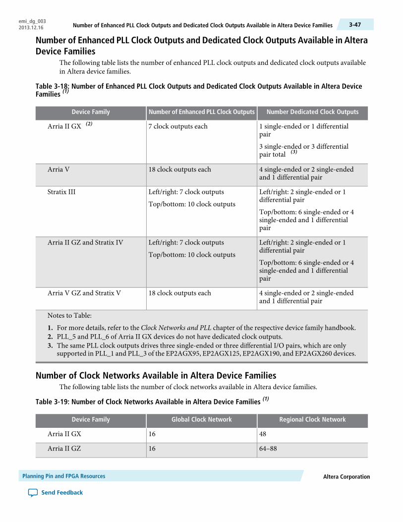
Number of Enhanced PLL Clock Outputs and Dedicated Clock Outputs Available in AlteraDevice Families
The following table lists the number of enhanced PLL clock outputs and dedicated clock outputs availablein Altera device families.
Table 3-18: Number of Enhanced PLL Clock Outputs and Dedicated Clock Outputs Available in Altera DeviceFamilies (1)
Number Dedicated Clock OutputsNumber of Enhanced PLL Clock OutputsDevice Family
1 single-ended or 1 differentialpair
3 single-ended or 3 differentialpair total (3)
7 clock outputs eachArria II GX (2)
4 single-ended or 2 single-endedand 1 differential pair
18 clock outputs eachArria V
Left/right: 2 single-ended or 1differential pair
Top/bottom: 6 single-ended or 4single-ended and 1 differentialpair
Left/right: 7 clock outputs
Top/bottom: 10 clock outputs
Stratix III
Left/right: 2 single-ended or 1differential pair
Top/bottom: 6 single-ended or 4single-ended and 1 differentialpair
Left/right: 7 clock outputs
Top/bottom: 10 clock outputs
Arria II GZ and Stratix IV
4 single-ended or 2 single-endedand 1 differential pair
18 clock outputs eachArria V GZ and Stratix V
Notes to Table:
1. For more details, refer to the Clock Networks and PLL chapter of the respective device family handbook.2. PLL_5 and PLL_6 of Arria II GX devices do not have dedicated clock outputs.3. The same PLL clock outputs drives three single-ended or three differential I/O pairs, which are only
supported in PLL_1 and PLL_3 of the EP2AGX95, EP2AGX125, EP2AGX190, and EP2AGX260 devices.
Number of Clock Networks Available in Altera Device FamiliesThe following table lists the number of clock networks available in Altera device families.
Table 3-19: Number of Clock Networks Available in Altera Device Families (1)
Regional Clock NetworkGlobal Clock NetworkDevice Family
4816Arria II GX
64–8816Arria II GZ
Altera CorporationPlanning Pin and FPGA Resources
Send Feedback
3-47Number of Enhanced PLL Clock Outputs and Dedicated Clock Outputs Available in Altera Device Familiesemi_dg_0032013.12.16

Regional Clock NetworkGlobal Clock NetworkDevice Family
8816Arria V
9216Arria V GZ
N/A16Cyclone V
64–8816Stratix III
64–8816Stratix IV
9216Stratix V
Note to Table:
1. For more information on the number of available clock network resources per device quadrant to betterunderstand the number of clock networks available for your interface, refer to the Clock Networks andPLL chapter of the respective device family handbook.
You must decide whether you need to share clock networks, PLL clock outputs, or PLLs if you areimplementing multiple memory interfaces.
Note:
Clock Network Usage in UniPHY-based Memory Interfaces—DDR2 and DDR3 SDRAM(1) (2)
The following table lists clock network usage in UniPHY-based memory interfaces for DDR2 and DDR3protocols.
Table 3-20: Clock Network Usage in UniPHY-based Memory Interfaces—DDR2 and DDR3 SDRAM
DDR2 SDRAMDDR3 SDRAM
DeviceHalf-RateHalf-Rate
Number of half-rate clockNumber of full-rate clock
Number of half-rate clock
Number of full-rate clock
1 global
1 regional
1 global
2 global
1 global
1 regional
3 globalStratix III
1 global
1 regional
1 regional
2 regional
1 global
1 regional
3 globalArria II GZ and StratixIV
2 global1 regional
2 regional
2 global1 global
2 regional
Arria V GZ and StratixV
Planning Pin and FPGA ResourcesAltera Corporation
Send Feedback
emi_dg_003Clock Network Usage in UniPHY-based Memory Interfaces—DDR2 and DDR3 SDRAM (1) (2)3-48 2013.12.16

DDR2 SDRAMDDR3 SDRAM
DeviceHalf-RateHalf-Rate
Number of half-rate clockNumber of full-rate clock
Number of half-rate clock
Number of full-rate clock
Notes to Table:
1. There are two additional regional clocks,pll_avl_clk andpll_config_clk for DDR2 and DDR3SDRAM with UniPHY memory interfaces.
2. In multiple interface designs with other IP, the clock network might need to be modified to get a designto fit. For more information, refer to the Clock Networks and PLLs chapter in the respective devicehandbooks.
Clock Network Usage in UniPHY-based Memory Interfaces—RLDRAM II, and QDR II andQDR II+ SRAM
The following table lists clock network usage in UniPHY-based memory interfaces for RLDRAM II, QDRII, and QDR II+ protocols.
Table 3-21: Clock Network Usage in UniPHY-based Memory Interfaces—RLDRAM II, and QDR II and QDR II+SRAM
QDR II/QDR II+ SRAMRLDRAM II
DeviceFull-RateHalf-RateFull-RateHalf-Rate
Number of full-rateclock
Number ofhalf-rate
clock
Number offull-rate clock
Number offull-rate clock
Number ofhalf-rate
clock
Number offull-rate clock
4 global2 global2 global———Arria II GX
1 global
2 regional
2 regional1 global
1 regional
1 global
2 regional
1 global
1 regional
2 regionalStratix III
1 global
2 regional
2 regional1 global
1 regional
1 global
2 regional
1 global
1 regional
2 regionalArria II GZ andStratix IV
For more information about the clocks used in UniPHY-based memory standards, refer to theFunctional Description—UniPHY chapter in volume 3 of the External Memory Interface Handbook.
Note:
Related InformationFunctional Description—UniPHY
PLL Usage for DDR, DDR2, and DDR3 SDRAM Without Leveling InterfacesThe following table lists PLL usage for DDR, DDR2, and DDR3 protocols without leveling interfaces.
Altera CorporationPlanning Pin and FPGA Resources
Send Feedback
3-49Clock Network Usage in UniPHY-based Memory Interfaces—RLDRAM II, and QDR II and QDR II+ SRAMemi_dg_0032013.12.16

Table 3-22: PLL Usage for DDR, DDR2, and DDR3 SDRAM Without Leveling Interfaces
Stratix III and Stratix IV DevicesArria II GX DevicesClock
• phy_clk_1x in half-rate designs• aux_half_rate_clk• PLL scan_clk
• phy_clk_1x in half-rate designs• aux_half_rate_clk• PLL scan_clk
C0
• mem_clk_2x• phy_clk_1x in full-rate designs• aux_full_rate_clk• mem_clk_2x to generate DQS and CK/CK#
signals• ac_clk_2x• cs_n_clk_2x
C1
• phy_clk_1x in full-rate designs• aux_full_rate_clk
• UnusedC2
• write_clk_2x• write_clk_2x (for DQ)• ac_clk_2x• cs_n_clk_2x
C3
• resync_clk_2x• resync_clk_2xC4
• measure_clk_1x• measure_clk_2xC5
• ac_clk_1x—C6
PLL Usage for DDR3 SDRAM With Leveling InterfacesThe following table lists PLL usage for DDR3 protocols with leveling interfaces.
Table 3-23: PLL Usage for DDR3 SDRAM With Leveling Interfaces
Stratix III and Stratix IV DevicesClock
• phy_clk_1x in half-rate designs• aux_half_rate_clk• PLL scan_clk
C0
• mem_clk_2xC1
• aux_full_rate_clkC2
• write_clk_2xC3
• resync_clk_2xC4
• measure_clk_1xC5
• ac_clk_1xC6
Planning Pin and FPGA ResourcesAltera Corporation
Send Feedback
emi_dg_003PLL Usage for DDR3 SDRAM With Leveling Interfaces3-50 2013.12.16

Using PLL GuidelinesWhen using PLL for external memory interfaces, you must consider the following guidelines:
• For the clock source, use the clock input pin specifically dedicated to the PLL that you want to use withyour external memory interface. The input and output pins are only fully compensated when you usethe dedicated PLL clock input pin. If the clock source for the PLL is not a dedicated clock input pin forthe dedicated PLL, you would need an additional clock network to connect the clock source to the PLLblock. Using additional clock network may increase clock jitter and degrade the timing margin.
• Pick a PLL and PLL input clock pin that are located on the same side of the device as the memory interfacepins.
• Share the DLL and PLL static clocks for multiple memory interfaces provided the controllers are on thesame or adjacent side of the device and run at the same memory clock frequency.
• If your design uses a dedicated PLL to only generate a DLL input reference clock, you must set the PLLmode to No Compensation in the Quartus II software to minimize the jitter, or the software forces thissetting automatically. The PLL does not generate other output, so it does not need to compensate for anyclock path.
• If your design cascades PLL, the source (upstream) PLL must have a low-bandwidth setting, while thedestination (downstream) PLL must have a high-bandwidth setting to minimize jitter. Altera does notrecommend using cascaded PLLs for external memory interfaces because your design gets accumulatedjitters. The memory output clock may violate the memory device jitter specification.
• Use cascading PLLs at your own risk. For more information, refer to “PLL Cascading”.• If you are using Arria II GX devices, for a single memory instance that spans two right-side quadrants,
use a middle-side PLL as the source for that interface.• If you are using Arria II GZ, Arria V GZ, Stratix III, Stratix IV, or Stratix V devices, for a single memory
instance that spans two top or bottom quadrants, use a middle top or bottom PLL as the source for thatinterface. The ten dual regional clocks that the single interface requires must not block the design usingthe adjacent PLL (if available) for a second interface.
Related InformationPLL Cascading on page 3-51
PLL CascadingArria II GZ PLLs, Stratix III PLLs, Stratix IV PLLs, Stratix V and Arria V GZ fractional PLLs (fPLLs), andthe two middle PLLs in Arria II GX EP2AGX95, EP2AGX125, EP2AGX190, and EP2AGX260 devices canbe cascaded using either the global or regional clock trees, or the cascade path between two adjacent PLLs.
Use cascading PLLs at your own risk. You should use faster memory devices to maximize timingmargins.
Note:
The UniPHY IP supports PLL cascading using the cascade path without any additional timing derating whenthe bandwidth and compensation rules are followed. The timing constraints and analysis assume that thereis no additional jitter due to PLL cascading when the upstream PLL uses no compensation and low bandwidth,and the downstream PLL uses no compensation and high bandwidth.
The UniPHY IP does not support PLL cascading using the global and regional clock networks. You canimplement PLL cascading at your own risk without any additional guidance and specifications from Altera.The Quartus II software does issue a critical warning suggesting use of the cascade path to minimize jitter,but does not explicitly state that Altera does not support cascading using global and regional clock networks.
Altera CorporationPlanning Pin and FPGA Resources
Send Feedback
3-51Using PLL Guidelinesemi_dg_0032013.12.16

Some Arria II GX devices (EP2AGX95, EP2AGX125, EP2AGX190, and EP2AGX260) have direct cascadepath for two middle right PLLs. Arria II GX PLLs have the same bandwidth options as Stratix IV GX leftand right PLLs.
DLLThe Altera memory interface IP uses one DLL. The DLL is located at the corner of the device and can sendthe control signals to shift the DQS pins on its adjacent sides for Stratix-series devices, or DQS pins in anyI/O banks in Arria II GX devices.
For example, the top-left DLL can shift DQS pins on the top side and left side of the device. The DLL generatesthe same phase shift resolution for both sides, but can generate different phase offset to the two differentsides, if needed. Each DQS pin can be configured to use or ignore the phase offset generated by the DLL.
The DLL cannot generate two different phase offsets to the same side of the device. However, you can usetwo different DLLs to for this functionality.
DLL reference clocks must come from either dedicated clock input pins located on either side of the DLLor from specific PLL output clocks. Any clock running at the memory frequency is valid for the DLLs.
To minimize the number of clocks routed directly on the PCB, typically this reference clock is sourced fromthe memory controllers PLL. In general, DLLs can use the PLLs directly adjacent to them (corner PLLs whenavailable) or the closest PLL located in the two sides adjacent to its location.
By default, the DLL reference clock in Altera external memory IP is from a PLL output.Note:
When designing for 780-pin packages with EP3SE80, EP3SE110, EP3SL150, EP4SE230, EP4SE360,EP4SGX180, and EP4SGX230 devices, the PLL to DLL reference clock connection is limited. DLL2 is isolatedfrom a direct PLL connection and can only receive a reference clock externally from pins CLK[11:4]p inEP3SE80, EP3SE110, EP3SL150, EP4SE230, and EP4SE360 devices. In EP4SGX180 and EP4SGX230 devices,DLL2 and DLL3 are not directly connected to PLL. DLL2 and DLL3 receive a reference clock externally frompins CLK[7:4]p and CLK[15:12]p respectively.
For more DLL information, refer to the respective device handbooks.
The DLL reference clock should be the same frequency as the memory interface, but the phase is not important.
The required DQS capture phase is optimally chosen based on operating frequency and external memoryinterface type (DDR, DDR2, DDR3 SDRAM, and QDR II SRAM, or RLDRAM II). As each DLL supportstwo possible phase offsets, two different memory interface types operating at the same frequency can easilyshare a single DLL. More may be possible, depending on the phase shift required.
Altera memory IP always specifies a default optimal phase setting, to override this setting, refer toImplementing and Parameterizing Memory IP .
When sharing DLLs, your memory interfaces must be of the same frequency. If the required phase shift isdifferent amongst the multiple memory interfaces, you can use a different delay chain in the DQS logic blockor use the DLL phase offset feature.
To simplify the interface to IP connections, multiple memory interfaces operating at the same frequencyusually share the same system and static clocks as each other where possible. This sharing minimizes thenumber of dedicated clock nets required and reduces the number of different clock domains found withinthe same design.
As each DLL can directly drive four banks, but each PLL only has complete C (output) counter coverage oftwo banks (using dual regional networks), situations can occur where a second PLL operating at the same
Planning Pin and FPGA ResourcesAltera Corporation
Send Feedback
emi_dg_003DLL3-52 2013.12.16

frequency is required. As cascaded PLLs increase jitter and reduce timing margin, you are advised to firstascertain if an alternative second DLL and PLL combination is not available and more optimal.
Select a DLL that is available for the side of the device where the memory interface resides. If you select aPLL or a PLL input clock reference pin that can also serve as the DLL input reference clock, you do not needan extra input pin for the DLL input reference clock.
Other FPGA ResourcesThe Altera memory interface IP uses FPGA fabric, including registers and the Memory Block to implementthe memory interface.
For resource utilization examples to ensure that you can fit your other modules in the device, refer to the“Resource Utilization” section in the Introduction to UniPHY IP chapter of the External Memory InterfaceHandbook.
One OCT calibration block is used if you are using the FPGA OCT feature in the memory interface.TheOCT calibration block uses two pins (RUP and RDN), or single pin (RZQ) (“OCT Support for Arria II GX,Arria II GZ, Arria V, Arria V GZ, Cyclone V, Stratix III, Stratix IV, and Stratix V Devices”). You can selectany of the available OCT calibration block as you do not need to place this block in the same bank or deviceside of your memory interface. The only requirement is that the I/O bank where you place the OCTcalibration block uses the same VCCIO voltage as the memory interface. You can share multiple memoryinterfaces with the same OCT calibration block if the VCCIO voltage is the same.
Related Information
• OCT Support for Arria II GX, Arria II GZ, Arria V, Arria V GZ, Cyclone V, Stratix III, Stratix IV,and Stratix V Devices on page 3-24
• Introduction to UniPHY IP
Document Revision History
ChangesVersionDate
• Removed references toALTMEMPHY and HardCopy.
• Removed references to Cyclone IIIand Cyclone IV devices.
2013.12.16December 2013
• Added Arria V GZ information.• Added RLDRAM 3 information.• Added LRDIMM information.
6.0November 2012
• Added LPDDR2 information.• Added Cyclone V information.• Added Feedback icon.
5.0June 2012
Altera CorporationPlanning Pin and FPGA Resources
Send Feedback
3-53Other FPGA Resourcesemi_dg_0032013.12.16

ChangesVersionDate
• Moved and reorganized PlanningPin andResource section to Volume2:Design Guidelines.
• Added Additional Guidelines forArria V GZ and Stratix V Devicessection.
• Added Arria V and Cyclone Vinformation.
4.0November 2011
• Moved Select a Device and MemoryIP Planning chapters to Volume 1.
• Added information about interfacepins.
• Added guidelines for using PLL.
3.0June 2011
• Added a new section on controllerefficiency.
• Added Arria II GX and Stratix Vinformation.
2.1December 2010
Updated information about UniPHY-based interfaces and Stratix V devices.
2.0July 2010
Initial release.1.0April 2010
Planning Pin and FPGA ResourcesAltera Corporation
Send Feedback
emi_dg_003Document Revision History3-54 2013.12.16