Embed Size (px)
Citation preview
PL-2303HX Edition (Chip Rev D) USB to Serial Bridge Controller Product Datasheet Document Revision: 1.4.3 Document Release: September 11, 2012
Prolific Technology Inc. 7F, No. 48, Sec. 3, Nan Kang Rd.
Nan Kang, Taipei 115, Taiwan, R.O.C.
Telephone: +886-2-2654-6363
Fax: +886-2-2654-6161
E-mail: [email protected]
Website: http://www.prolific.com.tw
Revised Date: September 11, 2012
ds_pl2303HXD_v1.4.3
PL-2303HX (Rev D) Product Datasheet - 2 - Document Version 1.4.3
Disclaimer All the information in this document is subject to change without prior notice. Prolific Technology Inc.
does not make any representations or any warranties (implied or otherwise) regarding the accuracy
and completeness of this document and shall in no event be liable for any loss of profit or any other
commercial damage, including but not limited to special, incidental, consequential, or other damages.
Trademarks The Prolific logo is a registered trademark of Prolific Technology Inc. All brand names and product
names used in this document are trademarks or registered trademarks of their respective holders.
Copyrights Copyright © 2005-2012 Prolific Technology Inc., All rights reserved.
No part of this document may be reproduced or transmitted in any form by any means without the
express written permission of Prolific Technology Inc.
Revised Date: September 11, 2012
ds_pl2303HXD_v1.4.3
PL-2303HX (Rev D) Product Datasheet - 3 - Document Version 1.4.3
Revision History
Revision Description Date 1.4.3 Modify Features and OS Driver Support List
Added QFN32 Reel Tape Information September 11, 2012
1.4.2 Modify Section 12.0 Ordering Information Part Number June 25, 2012 1.4.1 Modify Reel Tape Packing (MOQ) Information May 25, 2012 1.4 Added Windows 8 Driver Support
Added OTPROM Configuration Section Modified BaudRate Support Table Added Reference Schematic Diagram Added Chip Marking Information Added Tube Packing Information Added Worldwide Distributors Information
March 16, 2012
1.3 Added Windows 7 Logo Driver Information Modified Operating Temperature Characteristics Modified Baud Rate Settings Table
September 9, 2010
1.2 Sec. 9.0: Modified DC & Temperature Characteristics June 27, 2008 1.1 Added Windows Vista and XP Logo Driver information
Added USB-IF Logo TID information April 16, 2007
1.0B Sec. 4.2: Modified QFN diagram to add IC bottom PAD information
June 30, 2006
1.0A PL-2303HX (Chip Rev D) Datasheet – Formal Release November 23, 2005
Revised Date: September 11, 2012
ds_pl2303HXD_v1.4.3
PL-2303HX (Rev D) Product Datasheet - 4 - Document Version 1.4.3
Table of Contents
1.0 FEATURES........................................................................................................ 7
1.1 Royalty-Free Driver Support ................................................................................. 8
1.2 Product Applications ............................................................................................. 8
2.0 FUNCTIONAL BLOCK DIAGRAM .................................................................... 9
3.0 INTRODUCTION ............................................................................................. 10
4.0 PIN ASSIGNMENT OUTLINE ......................................................................... 11
4.1 SSOP28 Package .............................................................................................. 11
4.2 QFN32 Package................................................................................................. 12
5.0 PIN ASSIGNMENT & DESCRIPTION ............................................................. 13
5.1 SSOP28 Package .............................................................................................. 13
5.2 QFN32 Package................................................................................................. 14
6.0 OTPROM CONFIGURATION .......................................................................... 15
7.0 DATA FORMATS & PROGRAMMABLE BAUD RATE GENERATOR ............ 17
8.0 PL2303HXD REFERENCE SCHEMATIC DIAGRAM ..................................... 18
9.0 DC & TEMPERATURE CHARACTERISTICS ................................................. 19
9.1 Absolute Maximum Ratings ................................................................................ 19
9.2 DC Characteristics ............................................................................................. 19
9.3 Clock Characteristics ......................................................................................... 20
9.4 Temperature Characteristics .............................................................................. 21
9.5 Leakage Current and Capacitance ..................................................................... 21
9.6 Power-On Reset .................................................................................................. 21
10.0 OUTLINE DIAGRAM ....................................................................................... 22
10.1 SSOP28 Package .............................................................................................. 22
10.2 QFN32 Package ................................................................................................ 23
11.0 PACKING INFORMATION .............................................................................. 24
11.1 Carrier Tape (SSOP-28) ..................................................................................... 24
11.2 Carrier Tape (QFN32) ......................................................................................... 25
11.3 Reel Dimension .................................................................................................. 26
11.4 Tube Packing ..................................................................................................... 27
Revised Date: September 11, 2012
ds_pl2303HXD_v1.4.3
PL-2303HX (Rev D) Product Datasheet - 5 - Document Version 1.4.3
12.0 ORDERING AND CHIP MARKING INFORMATION ....................................... 28
13.0 CONTACT INFORMATION ............................................................................. 29
Revised Date: September 11, 2012
ds_pl2303HXD_v1.4.3
PL-2303HX (Rev D) Product Datasheet - 6 - Document Version 1.4.3
List of Figures Figure 2-1 Block Diagram of PL-2303HX (Rev D) ................................................................... 9 Figure 4-1 Pin Assignment Outline of PL-2303HX (Rev D) SSOP28 .................................... 11 Figure 4-2 Pin Assignment Outline of PL-2303HX (Rev D) QFN32 ....................................... 12 Figure 6-1 PL2303 EEPROM Writer Program ....................................................................... 15 Figure 8-1 PL2303HX (Chip Rev D) Reference Schematic Diagram .................................... 18 Figure 9-1 Power-On Reset Diagram.................................................................................... 21 Figure 10-1 Outline Diagram of PL-2303HX (Rev D) SSOP28 ............................................. 22 Figure 10-2 Outline Diagram of PL-2303HX (Rev D) QFN32 ................................................ 23 Figure 11-1 SSOP28 Carrier Tape ........................................................................................ 24 Figure 11-2 IC Reel Placements ........................................................................................... 24 Figure 11-3 QFN32 Carrier Tape .......................................................................................... 25 Figure 11-4 Reel Dimension ................................................................................................. 26 Figure 11-5 Tube Packing Dimension ................................................................................... 27 Figure 12-1 Chip Part Number Information (SSOP) .............................................................. 28
List of Tables Table 5-1 Pin Assignment & Description (SSOP28) .............................................................. 13 Table 5-2 Pin Assignment & Description (QFN32) ................................................................ 14 Table 6-1 EEPROM Writer Configuration .............................................................................. 15 Table 7-1 Supported Data Formats ....................................................................................... 17 Table 7-2 Baud Rate Settings (Supported by Driver) ............................................................ 17 Table 9-1 Absolute Maximum Ratings ................................................................................... 19 Table 9-2a Operating Voltage and Suspend Current ............................................................. 19 Table 9-2b 3.3V I/O Pins ....................................................................................................... 19 Table 9-2c [email protected] Serial I/O Pins .......................................................................... 20 Table 9-2d [email protected] Serial I/O Pins .......................................................................... 20 Table 9-2e [email protected] Serial I/O Pins .......................................................................... 20 Table 9-3 Clock Characteristics ............................................................................................ 20 Table 9-4 Temperature Characteristics ................................................................................. 21 Table 9-5 Leakage Current and Capacitance ........................................................................ 21 Table 9-6 Power-On Reset ................................................................................................... 21 Table 10-1 Package Dimension ............................................................................................ 22 Table 11-1 Reel Part Number Information ............................................................................. 26 Table 12-1 Ordering Information ........................................................................................... 28 Table 12-2 Chip Marking Information .................................................................................... 28
Revised Date: September 11, 2012
ds_pl2303HXD_v1.4.3
PL-2303HX (Rev D) Product Datasheet - 7 - Document Version 1.4.3
1.0 Features
Single-chip USB to Serial (RS232/RS422/RS485) asynchronous serial data transfer interface
Fully Compliant with USB Specification v2.0 (Full-Speed)
USB-IF Logo Compliant with TID 40000100
UHCI/OHCI (USB1.1), EHCI (USB 2.0), xHCI (USB 3.0) Host Controller Compatible
Integrated USB 1.1 Transceiver and 5V to 3.3V Regulator
Integrated 96MHz clock generator (No external crystal required)
Integrated OTPROM (One-Time Programming ROM) – no external EEPROM required. o For writing and storing customer USB VID/PID, Serial Number, Product String, and
other device startup configurations. (uses default settings if OTPROM is empty)
Supports USB to RS232 Serial UART Interface o Full-duplex transmitter and receiver (TXD and RXD) o Six MODEM control pins (RTS, CTS, DTR, DSR, DCD, and RI) o 5, 6, 7 or 8 data bits o Odd, Even, Mark, Space, or None parity mode o One, one and a half, or two stop bits o Parity error, frame error, and serial break detection o Programmable baud rate from 75 bps to 12M bps o External RS232 driver power down control o Independent power source for serial interface
Supports RS-422/RS-485 like serial interface (TXD, DTR_N, and RTS_N pins should be externally pulled-up to 5V)
Extensive Flow Control Mechanism o Adjustable high/low watermark level o Automatic hardware flow control with CTS/RTS or DSR/DTR o Automatic software flow control with XON/XOFF o Inbound data buffer overflow detection
Configurable 512-byte bi-directional data buffer o 256-byte outbound buffer and 256-byte inbound buffer; or o 128-byte outbound buffer and 384-byte inbound buffer
Supports Remote Wake-up from RS232 input pin signals (RI, RXD, DSR, DCD, CTS)
Four (4) General Purpose I/O (GP0, GP1, GP2, & GP3) pins and Four (4) Auxiliary General Purpose I/O (RI_N, DSR_N, DCD_N, & CTS_N) pins.
Supports Windows Selective Suspend by OTPROM configuration (Enable Remote Wakeup) o Suspends power of chip when idle (COM port is closed)
Provides royalty-free USB to Virtual COM Port (VCP) drivers for Windows, Mac, Linux
-40oC to 85oC Operating Temperature
Small footprint 28-pin SSOP or 32-pin QFN IC packages (RoHS compliant and Pb-free Green Compound
Revised Date: September 11, 2012
ds_pl2303HXD_v1.4.3
PL-2303HX (Rev D) Product Datasheet - 8 - Document Version 1.4.3
1.1 Royalty-Free Driver Support
Windows 8, 7, Vista, XP, 2000 (Microsoft Certified WHQL Drivers) o Windows Update Driver installation available in Windows Vista, 7, and 8 (32/64-bit)
Windows Server 2003, 2008, 2008 R2, 2012
Windows CE 4.2, 5.0, 6.0, and Windows Embedded Compact 7 o Requires customer SDK image file for customizing WinCE 6.0 and 7.0 drivers.
Windows XP Embedded (XPe), Point-of-Service (WEPOS), and POSReady
Mac OS 8/9, OS X (supports latest Mac OS X 10.8 Mountain Lion)
Linux/Android kernel 2.4.31 and above includes built-in drivers
Provides Driver Customization for Customer USB VID/PID and special baud rates
1.2 Product Applications
Single-chip upgrade solution for Legacy RS232 devices to USB interface
USB to RS232/RS422/RS485 converters/cables/dongles/adapters
Healthcare/Medical USB Interface Data Transfer Cable
Personal Infotainment/Media Player Docking USB Interface
Cellular/PDA USB Interface Data Transfer Cable
Serial-over-IP Wireless Solution
USB Barcode/Smart Card Readers
GPS/Navigation USB Interface
Point-of-Sale (POS) Terminals/Printers
PC Docking Station/Port Replicators
Industrial/Instrumentation/Automation Control USB Interface
USB Modem/Wireless/Zigbee USB Interface
Set-Top Box (STB) / Home Gateway USB Interface
MCU-based devices to USB interface
Revised Date: September 11, 2012
ds_pl2303HXD_v1.4.3
PL-2303HX (Rev D) Product Datasheet - 9 - Document Version 1.4.3
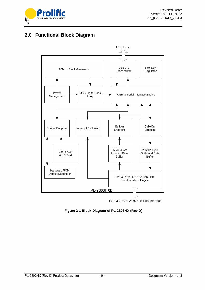
2.0 Functional Block Diagram
96MHz Clock Generator USB 1.1Transceiver
5 to 3.3VRegulator
PowerManagement
USB Digital LockLoop USB to Serial Interface Engine
Control Endpoint Interrupt Endpoint Bulk-inEndpoint
Bulk-OutEndpoint
256/384ByteInbound Data
Buffer
256/128ByteOutbound Data
Buffer
RS232 / RS-422 / RS-485 LikeSerial Interface Engine
256-BytesOTP ROM
Hardware ROMDefault Descriptor
PL-2303HXD
RS-232/RS-422/RS-485 Like Interface
USB Host
Figure 2-1 Block Diagram of PL-2303HX (Rev D)
Revised Date: September 11, 2012
ds_pl2303HXD_v1.4.3
PL-2303HX (Rev D) Product Datasheet - 10 - Document Version 1.4.3
3.0 Introduction PL-2303HX (Chip Rev D) or PL-2303HXD provides a convenient solution for connecting an RS232-like
full-duplex asynchronous serial device to any Universal Serial Bus (USB) capable host. PL-2303HXD
highly compatible drivers could simulate the traditional COM port on most operating systems allowing
the existing applications based on COM port to easily migrate and be made USB ready.
By taking advantage of USB bulk transfer mode, large data buffers, and automatic flow control,
PL-2303HXD is capable of achieving higher throughput compared to traditional UART (Universal
Asynchronous Receiver Transmitter) ports. When real RS232 signaling is not required, baud rate
higher than 115200 bps could be used for even higher performance. The flexible baud rate generator of
PL-2303HXD could be programmed to generate any rate between 75 bps to 12M bps.
PL-2303HXD is exclusively designed for mobile and embedded solutions in mind, providing a small
footprint that could easily fit in to any connectors and handheld devices. With very small power
consumption in either operating or suspend mode, PL-2303HXD is perfect for bus powered operation
with plenty of power left for the attached devices. Flexible signal level requirement on the RS232-like
serial port side also allows PL-2303HXD to connect directly to any 3.3V~1.8V range devices.
Revised Date: September 11, 2012
ds_pl2303HXD_v1.4.3
PL-2303HX (Rev D) Product Datasheet - 11 - Document Version 1.4.3
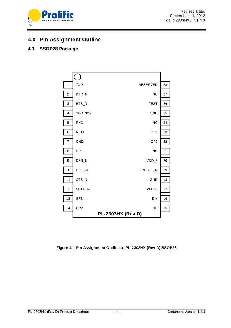
4.0 Pin Assignment Outline 4.1 SSOP28 Package
PL-2303HX (Rev D)
1 TXD
2 DTR_N
3 RTS_N
4 VDD_325
5 RXD
6 RI_N
7 GND
8 NC
9 DSR_N
10 DCD_N
11 CTS_N
12 SHTD_N
13 GP3
14 GP2
28RESERVED
27NC
26TEST
25GND
24NC
23GP1
22GP0
21NC
20VDD_5
19RESET_N
18GND
17VO_33
16DM
15DP
Figure 4-1 Pin Assignment Outline of PL-2303HX (Rev D) SSOP28
Revised Date: September 11, 2012
ds_pl2303HXD_v1.4.3
PL-2303HX (Rev D) Product Datasheet - 12 - Document Version 1.4.3
4.2 QFN32 Package
RT
S_N
N C
GN DG
ND
TE
ST
RE
SE
RV
ED
NC
NC
TX
D
DT
R_N
V D D _ 3 2 5
R XD
R I_N
GN D
V D D _ 3 3
D SR _N
D C D _N
C TS_N
SH
TD
_N GP
3
GP
2
NC
NC
DP
DM
NC
G P 1
G P 0
N C
V D D _ 5
R ESET_N
V O _ 3 3
PL-2303HXD
Exposed Die Pad connects to VO_33
1
Figure 4-2 Pin Assignment Outline of PL-2303HX (Rev D) QFN32
Warning: The exposed center die pad of the PL-2303HX QFN package is connected (bonded) to the
pin VO_33 so it is very important to design the PCB layout wherein this exposed die pad
won’t get grounded on the PCB when mounted.
Revised Date: September 11, 2012
ds_pl2303HXD_v1.4.3
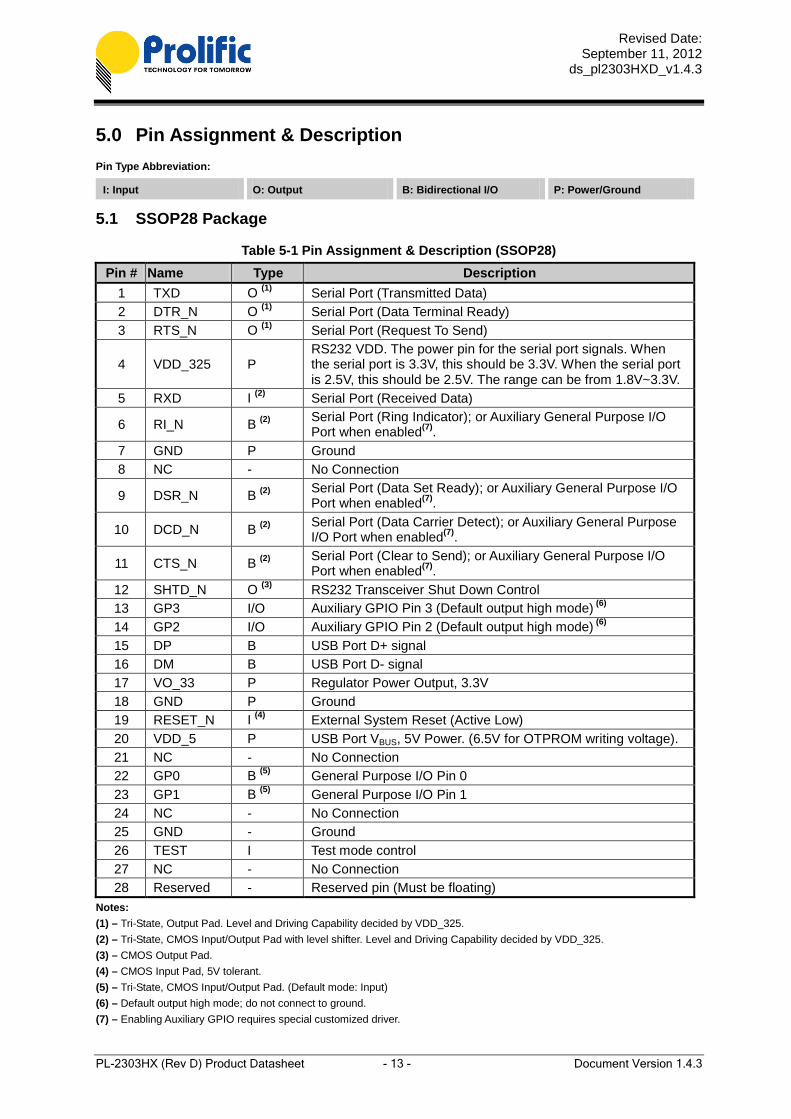
PL-2303HX (Rev D) Product Datasheet - 13 - Document Version 1.4.3
5.0 Pin Assignment & Description Pin Type Abbreviation:
I: Input O: Output B: Bidirectional I/O P: Power/Ground
5.1 SSOP28 Package
Table 5-1 Pin Assignment & Description (SSOP28) Pin # Name Type Description
1 TXD O (1) Serial Port (Transmitted Data) 2 DTR_N O (1) Serial Port (Data Terminal Ready) 3 RTS_N O (1) Serial Port (Request To Send)
4 VDD_325 P RS232 VDD. The power pin for the serial port signals. When the serial port is 3.3V, this should be 3.3V. When the serial port is 2.5V, this should be 2.5V. The range can be from 1.8V~3.3V.
5 RXD I (2) Serial Port (Received Data)
6 RI_N B (2) Serial Port (Ring Indicator); or Auxiliary General Purpose I/O Port when enabled(7).
7 GND P Ground 8 NC - No Connection
9 DSR_N B (2) Serial Port (Data Set Ready); or Auxiliary General Purpose I/O Port when enabled(7).
10 DCD_N B (2) Serial Port (Data Carrier Detect); or Auxiliary General Purpose I/O Port when enabled(7).
11 CTS_N B (2) Serial Port (Clear to Send); or Auxiliary General Purpose I/O Port when enabled(7).
12 SHTD_N O (3) RS232 Transceiver Shut Down Control 13 GP3 I/O Auxiliary GPIO Pin 3 (Default output high mode) (6) 14 GP2 I/O Auxiliary GPIO Pin 2 (Default output high mode) (6) 15 DP B USB Port D+ signal 16 DM B USB Port D- signal 17 VO_33 P Regulator Power Output, 3.3V 18 GND P Ground 19 RESET_N I (4) External System Reset (Active Low) 20 VDD_5 P USB Port VBUS, 5V Power. (6.5V for OTPROM writing voltage). 21 NC - No Connection 22 GP0 B (5) General Purpose I/O Pin 0 23 GP1 B (5) General Purpose I/O Pin 1 24 NC - No Connection 25 GND - Ground 26 TEST I Test mode control 27 NC - No Connection 28 Reserved - Reserved pin (Must be floating)
Notes: (1) – Tri-State, Output Pad. Level and Driving Capability decided by VDD_325. (2) – Tri-State, CMOS Input/Output Pad with level shifter. Level and Driving Capability decided by VDD_325. (3) – CMOS Output Pad. (4) – CMOS Input Pad, 5V tolerant. (5) – Tri-State, CMOS Input/Output Pad. (Default mode: Input) (6) – Default output high mode; do not connect to ground. (7) – Enabling Auxiliary GPIO requires special customized driver.
Revised Date: September 11, 2012
ds_pl2303HXD_v1.4.3
PL-2303HX (Rev D) Product Datasheet - 14 - Document Version 1.4.3
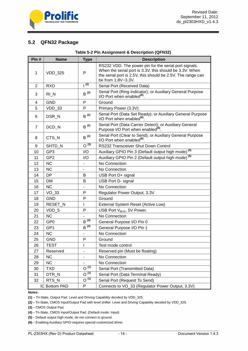
5.2 QFN32 Package
Table 5-2 Pin Assignment & Description (QFN32) Pin # Name Type Description
1 VDD_325 P
RS232 VDD. The power pin for the serial port signals. When the serial port is 3.3V, this should be 3.3V. When the serial port is 2.5V, this should be 2.5V. The range can be from 1.8V~3.3V.
2 RXD I (2) Serial Port (Received Data)
3 RI_N B (2) Serial Port (Ring Indicator); or Auxiliary General Purpose I/O Port when enabled(6).
4 GND P Ground 5 VDD_33 P Primary Power (3.3V)
6 DSR_N B (2) Serial Port (Data Set Ready); or Auxiliary General Purpose I/O Port when enabled(6).
7 DCD_N B (2) Serial Port (Data Carrier Detect); or Auxiliary General Purpose I/O Port when enabled(6).
8 CTS_N B (2) Serial Port (Clear to Send); or Auxiliary General Purpose I/O Port when enabled(6).
9 SHTD_N O (3) RS232 Transceiver Shut Down Control 10 GP3 I/O Auxiliary GPIO Pin 3 (Default output high mode) (5) 11 GP2 I/O Auxiliary GPIO Pin 2 (Default output high mode) (5) 12 NC - No Connection 13 NC - No Connection 14 DP B USB Port D+ signal 15 DM B USB Port D- signal 16 NC - No Connection 17 VO_33 P Regulator Power Output, 3.3V 18 GND P Ground 19 RESET_N I External System Reset (Active Low) 20 VDD_5 P USB Port VBUS, 5V Power. 21 NC - No Connection 22 GP0 B (4) General Purpose I/O Pin 0 23 GP1 B (4) General Purpose I/O Pin 1 24 NC - No Connection 25 GND P Ground 26 TEST I Test mode control 27 Reserved - Reserved pin (Must be floating) 28 NC - No Connection 29 NC - No Connection 30 TXD O (1) Serial Port (Transmitted Data) 31 DTR_N O (1) Serial Port (Data Terminal Ready) 32 RTS_N O (1) Serial Port (Request To Send)
IC Bottom PAD P Connects to VO_33 (Regulator Power Output, 3.3V) Notes: (1) – Tri-State, Output Pad. Level and Driving Capability decided by VDD_325. (2) – Tri-State, CMOS Input/Output Pad with level shifter. Level and Driving Capability decided by VDD_325. (3) – CMOS Output Pad. (4) – Tri-State, CMOS Input/Output Pad. (Default mode: Input) (5) – Default output high mode; do not connect to ground. (6) – Enabling Auxiliary GPIO requires special customized driver.
Revised Date: September 11, 2012
ds_pl2303HXD_v1.4.3
PL-2303HX (Rev D) Product Datasheet - 15 - Document Version 1.4.3
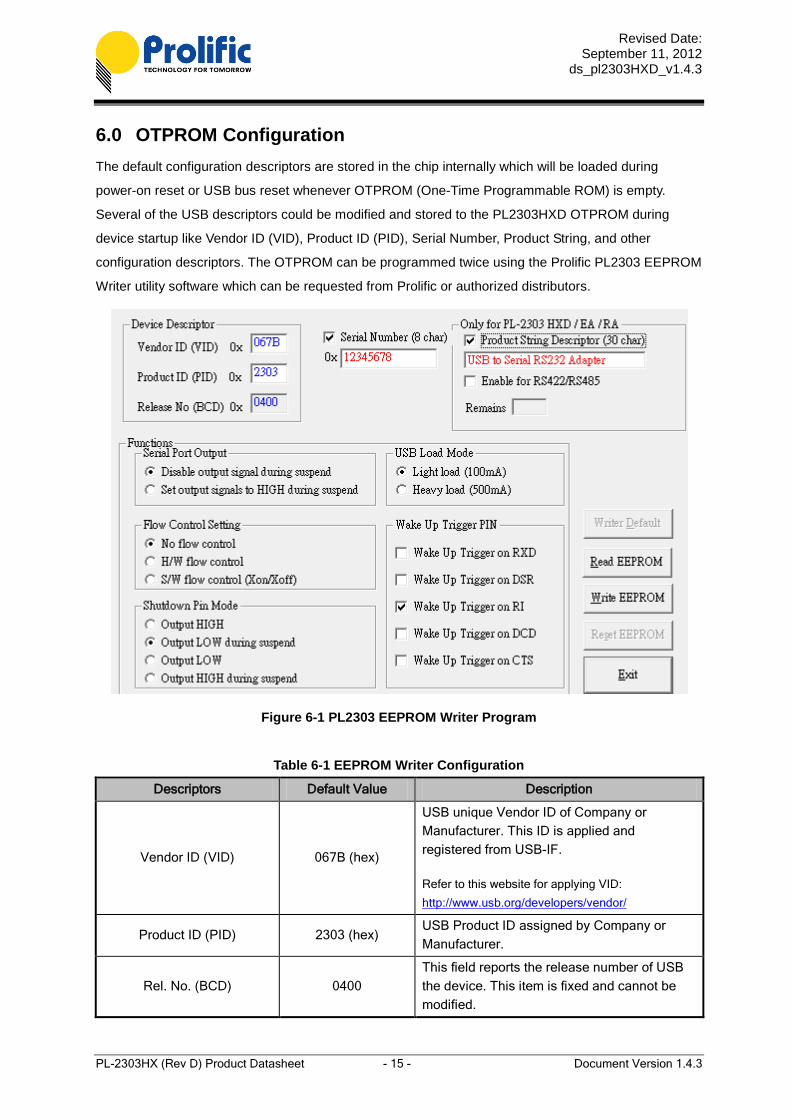
6.0 OTPROM Configuration The default configuration descriptors are stored in the chip internally which will be loaded during
power-on reset or USB bus reset whenever OTPROM (One-Time Programmable ROM) is empty.
Several of the USB descriptors could be modified and stored to the PL2303HXD OTPROM during
device startup like Vendor ID (VID), Product ID (PID), Serial Number, Product String, and other
configuration descriptors. The OTPROM can be programmed twice using the Prolific PL2303 EEPROM
Writer utility software which can be requested from Prolific or authorized distributors.
Figure 6-1 PL2303 EEPROM Writer Program
Table 6-1 EEPROM Writer Configuration
Descriptors Default Value Description
Vendor ID (VID) 067B (hex)
USB unique Vendor ID of Company or Manufacturer. This ID is applied and registered from USB-IF.
Refer to this website for applying VID:
http://www.usb.org/developers/vendor/
Product ID (PID) 2303 (hex) USB Product ID assigned by Company or Manufacturer.
Rel. No. (BCD) 0400 This field reports the release number of USB the device. This item is fixed and cannot be modified.
Revised Date: September 11, 2012
ds_pl2303HXD_v1.4.3
PL-2303HX (Rev D) Product Datasheet - 16 - Document Version 1.4.3
Serial No. (8 hex characters) Disabled
This field sets the product USB serial number. Entering a unique serial number allows the device to be assigned the same COM Port number even when plug to other USB ports of the same PC.
Product String Descriptor None
This field when entered will be the string displayed by Windows and other OS when device is first detected and before driver is loaded or driver not installed.
Enable for RS422/RS485 Disabled Enable this for RS422 or RS485 support.
Remains 2
PL2303HXD has an integrated OTPROM which allows to write EEPROM settings without the use of an external one. However, the OTPROM can only be written twice and cannot be erased. PL2303HXD does not support external EEPROM.
Functions Default Value Description
Serial Port Output Disable This option allows setting the serial port output pin signals (TXD, RTS, DTR) to HIGH during suspend mode.
USB Load Mode Light Load (100mA) This option sets the USB device maximum power if 100mA (low-power) or 500mA (high power).
Flow Control Setting No Flow Control
This option allows to set the flow control initial setting to none, H/W, or S/W control.
Note: H/W and S/W flow control can also be set and configured on customer/user serial communication software.
Wakeup Trigger Pin Wakeup trigger on
RI
This option allows setting the trigger pin for remote wakeup function. When in suspend mode, changes on the enabled serial port input signals could trigger a wakeup event.
NOTE: To support Selective Suspend function, you
need to write and enable this option in OTPROM.
Shutdown Pin Mode Output LOW during
suspend
This option allows setting the Shutdown pin mode to Output HIGH or LOW on normal mode or Suspend mode.
Revised Date: September 11, 2012
ds_pl2303HXD_v1.4.3
PL-2303HX (Rev D) Product Datasheet - 17 - Document Version 1.4.3
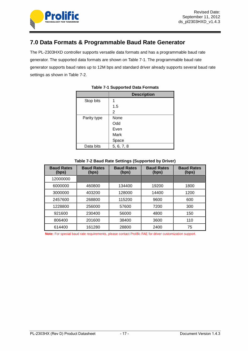
7.0 Data Formats & Programmable Baud Rate Generator The PL-2303HXD controller supports versatile data formats and has a programmable baud rate
generator. The supported data formats are shown on Table 7-1. The programmable baud rate
generator supports baud rates up to 12M bps and standard driver already supports several baud rate
settings as shown in Table 7-2.
Table 7-1 Supported Data Formats Description
Stop bits 1 1.5 2
Parity type None Odd Even Mark Space
Data bits 5, 6, 7, 8
Table 7-2 Baud Rate Settings (Supported by Driver) Baud Rates
(bps) Baud Rates
(bps) Baud Rates
(bps) Baud Rates
(bps) Baud Rates
(bps) 12000000 6000000 460800 134400 19200 1800 3000000 403200 128000 14400 1200 2457600 268800 115200 9600 600 1228800 256000 57600 7200 300 921600 230400 56000 4800 150 806400 201600 38400 3600 110 614400 161280 28800 2400 75
Note: For special baud rate requirements, please contact Prolific FAE for driver customization support.
Revised Date: September 11, 2012
ds_pl2303HXD_v1.4.3
PL-2303HX (Rev D) Product Datasheet - 18 - Document Version 1.4.3
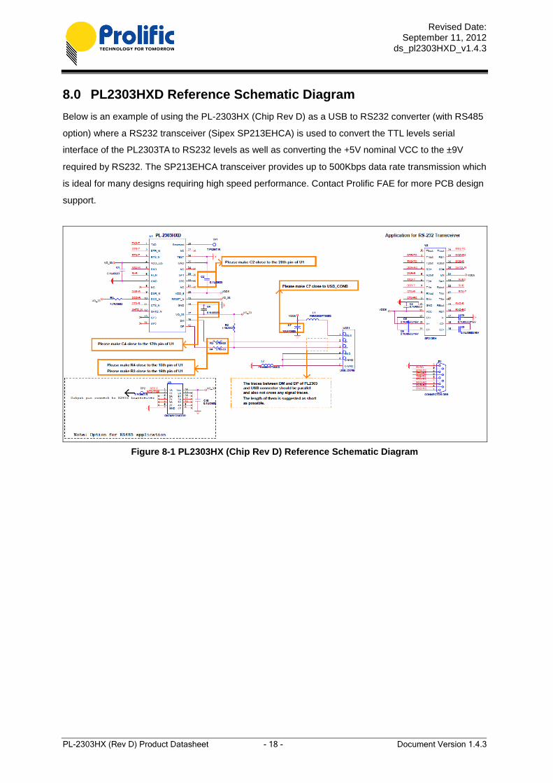
8.0 PL2303HXD Reference Schematic Diagram Below is an example of using the PL-2303HX (Chip Rev D) as a USB to RS232 converter (with RS485
option) where a RS232 transceiver (Sipex SP213EHCA) is used to convert the TTL levels serial
interface of the PL2303TA to RS232 levels as well as converting the +5V nominal VCC to the ±9V
required by RS232. The SP213EHCA transceiver provides up to 500Kbps data rate transmission which
is ideal for many designs requiring high speed performance. Contact Prolific FAE for more PCB design
support.
Figure 8-1 PL2303HX (Chip Rev D) Reference Schematic Diagram
Revised Date: September 11, 2012
ds_pl2303HXD_v1.4.3
PL-2303HX (Rev D) Product Datasheet - 19 - Document Version 1.4.3
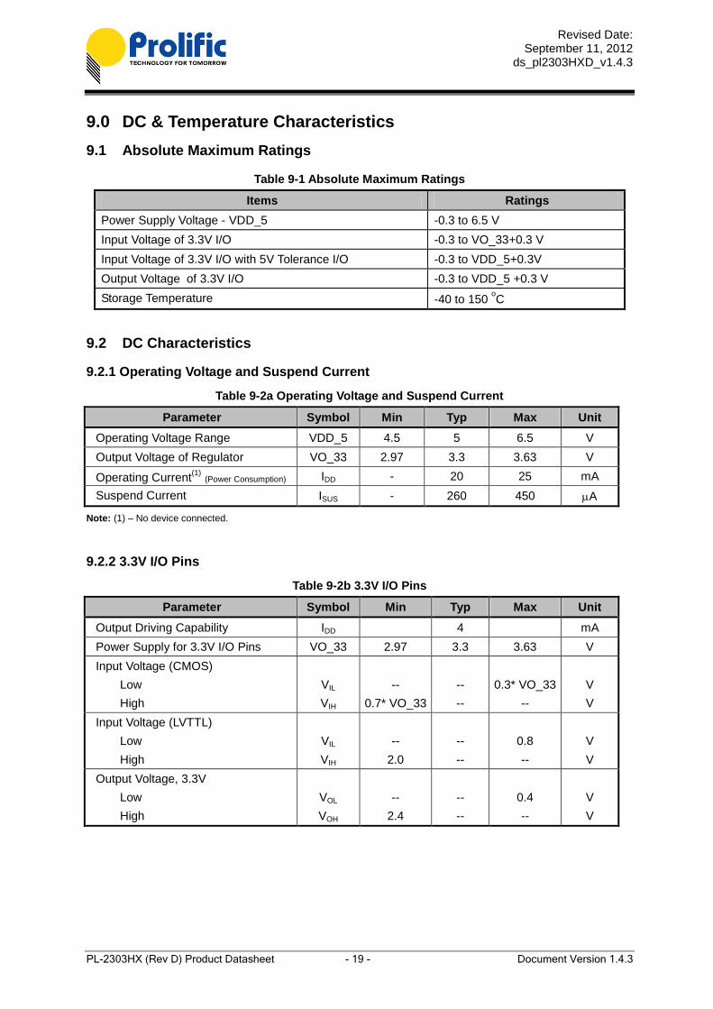
9.0 DC & Temperature Characteristics 9.1 Absolute Maximum Ratings
Table 9-1 Absolute Maximum Ratings
Items Ratings Power Supply Voltage - VDD_5 -0.3 to 6.5 V Input Voltage of 3.3V I/O -0.3 to VO_33+0.3 V Input Voltage of 3.3V I/O with 5V Tolerance I/O -0.3 to VDD_5+0.3V Output Voltage of 3.3V I/O -0.3 to VDD_5 +0.3 V Storage Temperature -40 to 150 oC
9.2 DC Characteristics
9.2.1 Operating Voltage and Suspend Current
Table 9-2a Operating Voltage and Suspend Current
Parameter Symbol Min Typ Max Unit Operating Voltage Range VDD_5 4.5 5 6.5 V Output Voltage of Regulator VO_33 2.97 3.3 3.63 V
Operating Current(1) (Power Consumption) IDD - 20 25 mA Suspend Current ISUS - 260 450 µA
Note: (1) – No device connected.
9.2.2 3.3V I/O Pins
Table 9-2b 3.3V I/O Pins
Parameter Symbol Min Typ Max Unit Output Driving Capability IDD 4 mA Power Supply for 3.3V I/O Pins VO_33 2.97 3.3 3.63 V Input Voltage (CMOS) Low High
VIL VIH
--
0.7* VO_33
-- --
0.3* VO_33
--
V V
Input Voltage (LVTTL) Low High
VIL VIH
--
2.0
-- --
0.8 --
V V
Output Voltage, 3.3V Low High
VOL VOH
--
2.4
-- --
0.4 --
V V
Revised Date: September 11, 2012
ds_pl2303HXD_v1.4.3
PL-2303HX (Rev D) Product Datasheet - 20 - Document Version 1.4.3
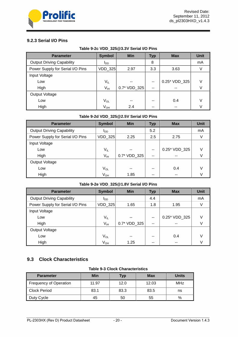
9.2.3 Serial I/O Pins
Table 9-2c [email protected] Serial I/O Pins
Parameter Symbol Min Typ Max Unit Output Driving Capability IDD 8 mA Power Supply for Serial I/O Pins VDD_325 2.97 3.3 3.63 V Input Voltage Low High
VIL VIH
--
0.7* VDD_325
-- --
0.25* VDD_325
--
V V
Output Voltage
Low High
VOL VOH
--
2.4
-- --
0.4 --
V V
Table 9-2d [email protected] Serial I/O Pins
Parameter Symbol Min Typ Max Unit Output Driving Capability IDD 5.2 mA Power Supply for Serial I/O Pins VDD_325 2.25 2.5 2.75 V Input Voltage Low High
VIL VIH
--
0.7* VDD_325
-- --
0.25* VDD_325
--
V V
Output Voltage Low High
VOL VOH
--
1.85
-- --
0.4 --
V V
Table 9-2e [email protected] Serial I/O Pins
Parameter Symbol Min Typ Max Unit Output Driving Capability IDD 4.4 mA Power Supply for Serial I/O Pins VDD_325 1.65 1.8 1.95 V Input Voltage Low High
VIL VIH
--
0.7* VDD_325
-- --
0.25* VDD_325
--
V V
Output Voltage Low High
VOL VOH
--
1.25
-- --
0.4 --
V V
9.3 Clock Characteristics
Table 9-3 Clock Characteristics Parameter Min Typ Max Units
Frequency of Operation 11.97 12.0 12.03 MHz
Clock Period 83.1 83.3 83.5 ns
Duty Cycle 45 50 55 %
Revised Date: September 11, 2012
ds_pl2303HXD_v1.4.3
PL-2303HX (Rev D) Product Datasheet - 21 - Document Version 1.4.3
9.4 Temperature Characteristics
Table 9-4 Temperature Characteristics
Parameter Symbol Min Typ Max Unit Operating Temperature -- -40 -- 85 oC Junction Operation Temperature TJ -40 25 105 oC
9.5 Leakage Current and Capacitance
Table 9-5 Leakage Current and Capacitance
Parameter Symbol Min Typ Max Unit Input Leakage Current*1 IL -10 ±1 10 µA Tri-state Leakage Current Ioz -10 ±1 10 µA Input Capacitance CIN -- 2.8 -- pF Output Capacitance COUT 2.7 -- 4.9 pF Bi-directional Buffer Capacitance CBID 2.7 -- 4.9 pF
*1. No pull-up or pull-down resistor.
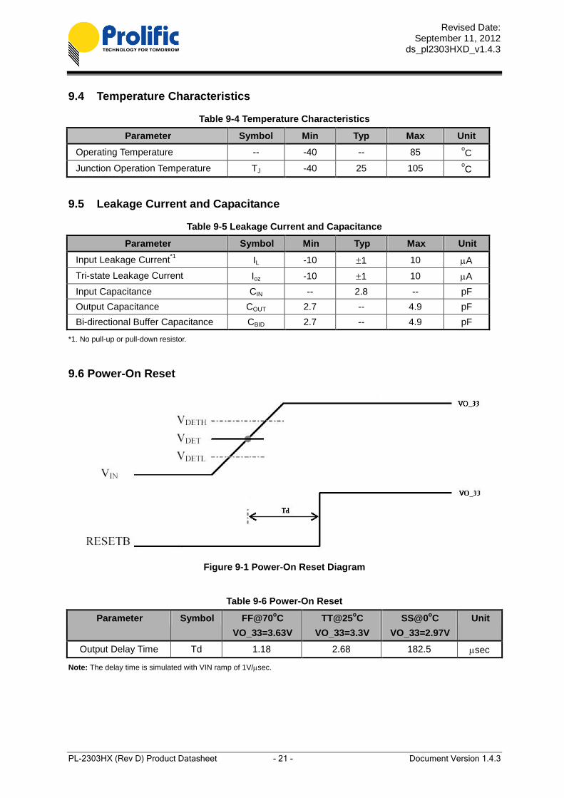
9.6 Power-On Reset
Figure 9-1 Power-On Reset Diagram
Table 9-6 Power-On Reset
Parameter Symbol FF@70oC VO_33=3.63V
TT@25oC VO_33=3.3V
SS@0oC VO_33=2.97V
Unit
Output Delay Time Td 1.18 2.68 182.5 µsec
Note: The delay time is simulated with VIN ramp of 1V/µsec.
Revised Date: September 11, 2012
ds_pl2303HXD_v1.4.3
PL-2303HX (Rev D) Product Datasheet - 22 - Document Version 1.4.3
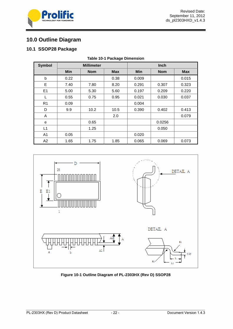
10.0 Outline Diagram 10.1 SSOP28 Package
Table 10-1 Package Dimension
Symbol Millimeter Inch Min Nom Max Min Nom Max
b 0.22 0.38 0.009 0.015 E 7.40 7.80 8.20 0.291 0.307 0.323 E1 5.00 5.30 5.60 0.197 0.209 0.220 L 0.55 0.75 0.95 0.021 0.030 0.037
R1 0.09 0.004 D 9.9 10.2 10.5 0.390 0.402 0.413 A 2.0 0.079 e 0.65 0.0256
L1 1.25 0.050 A1 0.05 0.020 A2 1.65 1.75 1.85 0.065 0.069 0.073
Figure 10-1 Outline Diagram of PL-2303HX (Rev D) SSOP28
Revised Date: September 11, 2012
ds_pl2303HXD_v1.4.3
PL-2303HX (Rev D) Product Datasheet - 23 - Document Version 1.4.3
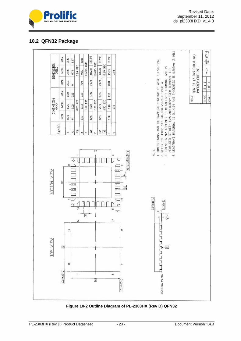
10.2 QFN32 Package
Figure 10-2 Outline Diagram of PL-2303HX (Rev D) QFN32
Revised Date: September 11, 2012
ds_pl2303HXD_v1.4.3
PL-2303HX (Rev D) Product Datasheet - 24 - Document Version 1.4.3
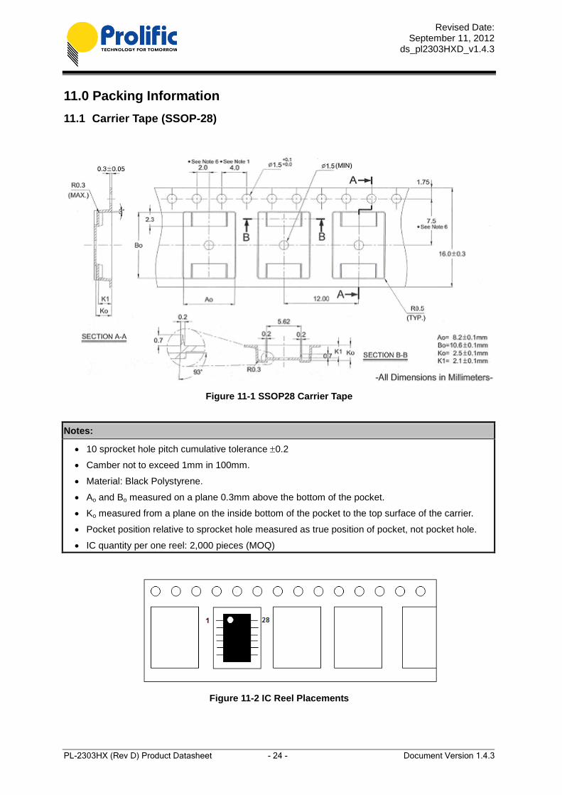
11.0 Packing Information 11.1 Carrier Tape (SSOP-28)
Figure 11-1 SSOP28 Carrier Tape
Notes:
• 10 sprocket hole pitch cumulative tolerance ±0.2
• Camber not to exceed 1mm in 100mm.
• Material: Black Polystyrene.
• Ao and Bo measured on a plane 0.3mm above the bottom of the pocket.
• Ko measured from a plane on the inside bottom of the pocket to the top surface of the carrier.
• Pocket position relative to sprocket hole measured as true position of pocket, not pocket hole.
• IC quantity per one reel: 2,000 pieces (MOQ)
Figure 11-2 IC Reel Placements
Revised Date: September 11, 2012
ds_pl2303HXD_v1.4.3
PL-2303HX (Rev D) Product Datasheet - 25 - Document Version 1.4.3
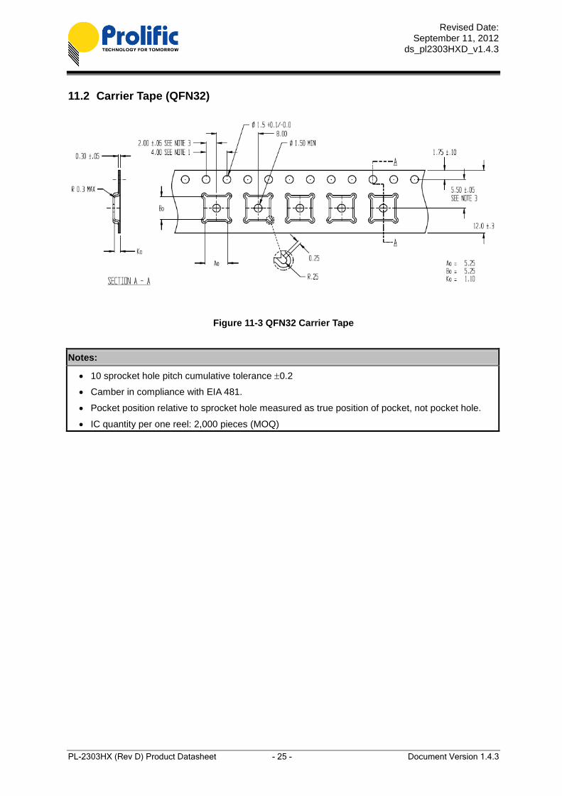
11.2 Carrier Tape (QFN32)
Figure 11-3 QFN32 Carrier Tape
Notes:
• 10 sprocket hole pitch cumulative tolerance ±0.2
• Camber in compliance with EIA 481.
• Pocket position relative to sprocket hole measured as true position of pocket, not pocket hole.
• IC quantity per one reel: 2,000 pieces (MOQ)
Revised Date: September 11, 2012
ds_pl2303HXD_v1.4.3
PL-2303HX (Rev D) Product Datasheet - 26 - Document Version 1.4.3
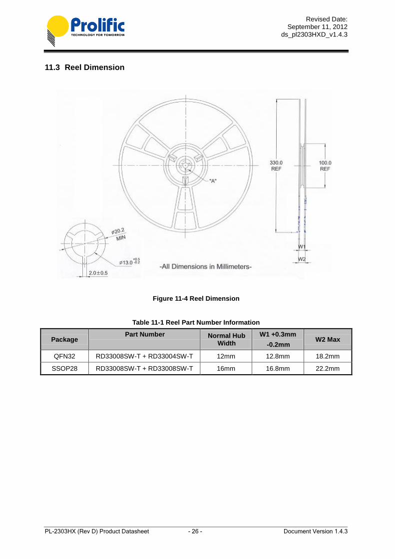
11.3 Reel Dimension
Figure 11-4 Reel Dimension
Table 11-1 Reel Part Number Information
Package Part Number Normal Hub
Width W1 +0.3mm
-0.2mm W2 Max
QFN32 RD33008SW-T + RD33004SW-T 12mm 12.8mm 18.2mm
SSOP28 RD33008SW-T + RD33008SW-T 16mm 16.8mm 22.2mm
Revised Date: September 11, 2012
ds_pl2303HXD_v1.4.3
PL-2303HX (Rev D) Product Datasheet - 27 - Document Version 1.4.3
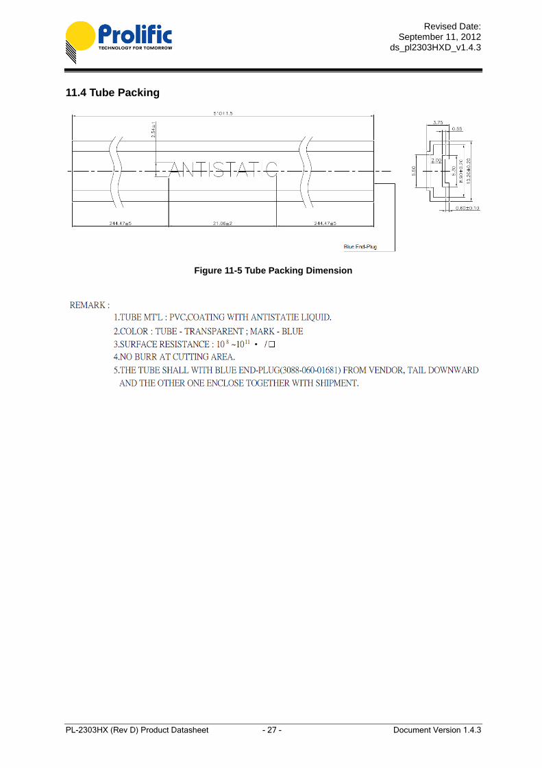
11.4 Tube Packing
Figure 11-5 Tube Packing Dimension
Revised Date: September 11, 2012
ds_pl2303HXD_v1.4.3
PL-2303HX (Rev D) Product Datasheet - 28 - Document Version 1.4.3
12.0 Ordering and Chip Marking Information Table 12-1 Ordering Information
Part Number Package Type PL-2303HXD LF 28-pin SSOP (Lead Free or Pb-Free) PL-2303HXD QFN32 LF 32-pin QFN (Lead Free or Pb-Free)
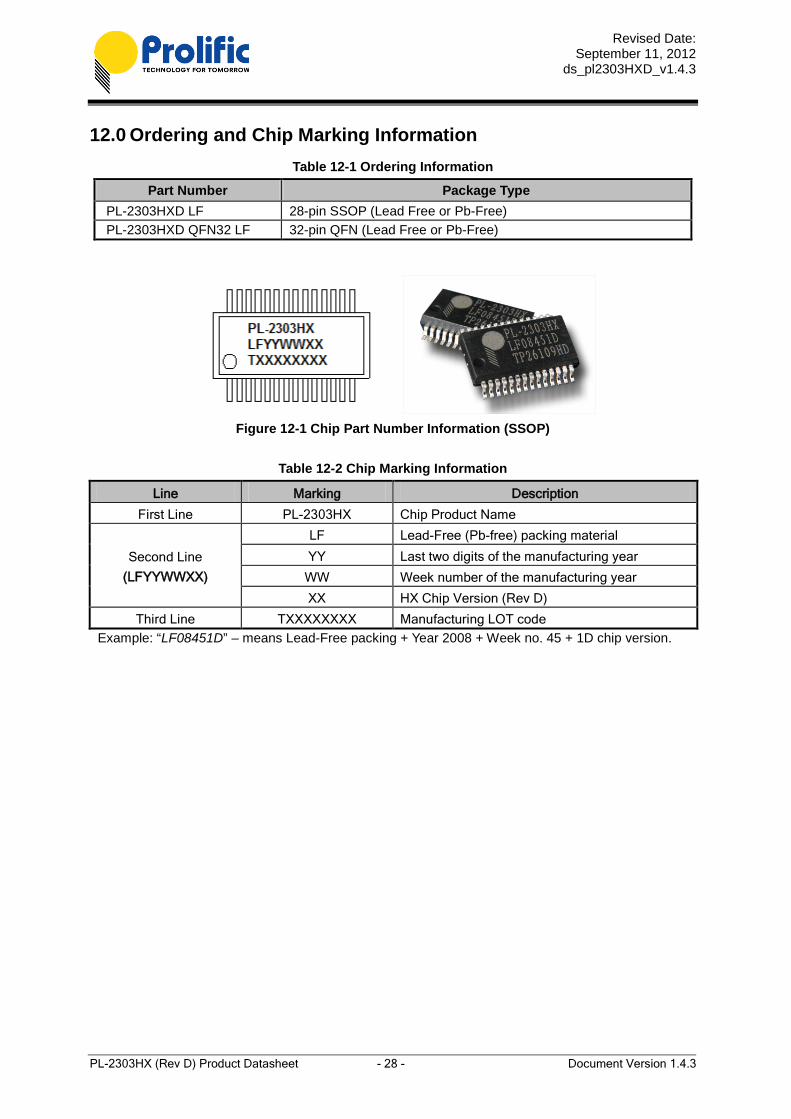
Figure 12-1 Chip Part Number Information (SSOP)
Table 12-2 Chip Marking Information
Line Marking Description
First Line PL-2303HX Chip Product Name
Second Line
(LFYYWWXX)
LF Lead-Free (Pb-free) packing material
YY Last two digits of the manufacturing year
WW Week number of the manufacturing year
XX HX Chip Version (Rev D)
Third Line TXXXXXXXX Manufacturing LOT code
Example: “LF08451D” – means Lead-Free packing + Year 2008 + Week no. 45 + 1D chip version.
Revised Date: September 11, 2012
ds_pl2303HXD_v1.4.3
PL-2303HX (Rev D) Product Datasheet - 29 - Document Version 1.4.3
13.0 Contact Information Taiwan Headquarter 7F, No.48, Sec. 3, Nan Kang Rd., Nan Kang, Taipei, Taiwan 115, R.O.C. Tel: +886-2-2654-6363 Fax: +886-2-2654-6161 Website: www.prolific.com.tw E-mail: [email protected]
Shenzhen Office Room 1908, Building, No.A. jiahehuaqiang Building, Shennanzhong Rd. Futian District, Shenzhen, China Tel: +86-1350-285-4191 E-mail: [email protected]
Distributors Contact: http://www.prolific.com.tw/eng/contact-distributors.asp
Taiwan Distributors Maxtek Technology Co., Ltd. 5F, No. 13-20, Sec. 6, Ming-Chuang E.RD., Nei-Hu, Taipei, Taiwan, R.O.C. Tel: +886-2-2794-6060 Ext.662 Fax: +886-2-8792-8921 Website: http://www.maxtek-icrep.com.tw E-mail: [email protected] Morrihan International Corp. 4F, No. 3-2, YuanCyu Street, NanKang District , Taipei 115, Taiwan, R.O.C. Tel: +886-2-2788-5511 Fax: +886-2-2788-9366 Website: http://www.morrihan.com U-CHEER Company Co., Ltd. 4F, No. 48, Chow-Tze ST., Nei-Hu, Taipei, Taiwan, R.O.C. Tel: +886-2-8797-6789 Fax: +886-2-8797-3388 E-mail: [email protected]
USA and Canada ProlificUSA.com / Tectona Electronics Inc. 250 Wyecroft Road, Unit 6, Oakville, Ontario, Canada L6K 3T7 Tel: +905-827-2206 Fax: +905-847-9412 Corporate Website: http://www.tectona.com Product Website: http://www.prolificUSA.com
Japan Hitachi High-Tech Trading Corporation 1-24-14, Nishi-Shimbashi, Minato-ku, Tokyo, 105-8418 Japan Dept.: Electronic Devices 4th Dept., Electonic Devices Sales Div Tel: +81-3-3504-3859 Fax: +81-3-3504-7903 Website: http://www.hitachi-hitec-trading.com
Revised Date: September 11, 2012
ds_pl2303HXD_v1.4.3
PL-2303HX (Rev D) Product Datasheet - 30 - Document Version 1.4.3
China Lacewood International Corp. Hong Kong Office Unit B1-B3, 21/F, Block B, Kong Nam Industrial Building, 603-609 Castle peak Road, Tsuen Wan N.T, Hong Kong Tel: +852-2690-9898 Fax: +852-2690-9300 Shenzhen Office Room401-3,East, CEC Information Building, No.1 Xin Wen Road, Shenzhen, P.R.C., 518034 Tel:+86-755-8296-7018 Fax: +86-775-8330-7119 Shanghai Office Rm 208,District B, Building 3,NO.7,Guiqin Rd, Xuhui Area, Shanghai Tel : +86-21-5426-2182 ~6 Fax: +86-21-5426-2180
China Freelink Asia Limited Room 307, 3F Block6, AnHua Industrial Zone, Tairan 8th Road, CheGongMiao, Futian District, Shenzhen, China Tel: +86-755-8302-0469
China Shenzhen Shiqixinji Science and Technology Co., Ltd. Room 1908, Building NO.A, Jiahehuaqiang Building, Shennanzhong Rd., Futian District, Shenzhen, China Tel: +86-755-8329-5310
Korea Nevora Technology Rm 502, Citylife, 441, Amsa-Dong, Kangdong-Gu, Seoul, 134-855, Korea Tel: +82-2-3426-0050 Fax: +82-2-3426-0070 Website: http://www.nevora.co.kr T&C Semitech Co.,LTD #703 J-dong, Gongku-sangga, 636-62, Kuro-dong, Kuro-ku, Seoul. Korea Tel: +82-2-2672-9531 Fax: +82-2-2672-9532 Website: http://www.tncsemi.co.kr