Embed Size (px)
Citation preview

T O S 7 2 1 0 S ( S P E C 8 0 7 7 6 )
Capable of setting within the range of 50 Vdc to 2000 Vdc (resolution 1 V)Ability to switch the applied voltage polarity instantly by the switch on the front panel
The output is floating from the ground potential. Capable of measuring the current value between measurement points.
S A F E T Y T E S T E R
PID Insulation Tester(Potential Induced Degradation)
TOS7210S
SAFETY TESTER
NEW

2
TOS7210S [SPEC80776]
You can set the test voltage that is appliedto the DUT within the range of 50 Vdc to 2000 Vdc
(resolution 1 V). In addition, an insulation resistancetest of the electricity/electronic components or
the electricity/electronic devices is alsopossible besides the voltagespecified in JIS C 1302:1994.In the range of 50 V to 1000 V,
the output properties are complied to JIS C 1302:1994.
Capable of arbitrary setting
of the output voltage
PID Insulation Tester
To evaluate the PID effect of the PV module!
You can easily change the output polarityby the switch on the front panel.
The PID deterioration is a reversible phenomenonthat may recover after the reverse bias voltage is applied.
The polarity switching is a convenient functionthat can avoid a wiring change that connects
to the DUT. In addition, switchingby the external control through
the RS232C interface is also possible.
Polarity switching function
NEW
Conceptual diagram of test
Back sheetterminal box
Connection tothe solarcell frame
Connecting the positive polarity andthe negative polarity of the terminal box as one unit
Connects TOS7210S andthe solar cell module
with an attached shield cable.
The PID insulation tester (TOS7210S) is designed based on the insulation resistance tester (TOS7200) to carry out the evaluation of the PID (Potential Induced Degradation) effect of the PV module precisely and efficiently. Being equipped with the output ability of 2000 V and the ammeter with nA resolution as well as a polarity switching function, the TOS7210S is also applicable not only to the PID evaluation but also the evaluation of the insulators that requires a high sensitivity of measurement. The tester is equipped with the panel memory that is externally accessible and RS232C interface as standard; it can be flexibly compatible with the automated system.
*
*Potential Induced Degradation

3
The PID effect is a phenomenon that the amount of power generation by a cell remarkably decreases when high voltage is applied between the solar cell and the frame for long hours. It is supposed that the higher the applied voltage is and/or the higher and more humid the environment is, the further deterioration accelerates. For example, the potential difference in the string becomes extremely higher when the number of sheets that are connected in series increases even if the output voltage of the crystalline silicon solar cell module is just tens of volts. On the other hand, the grounding methods of the PCS (Power Conditioning System) that connects to the system as an AC power supply varies according to the type of PCS. In recent years, the transformerless method, where the input side is in the floating method (the negative polarity is not connected to the ground) is increasing. In this case, a high potential difference occurs between the cell and the ground. Regarding the crystalline silicon solar cell module, it is proved that the cell having a higher negative electric potential than that of the frame (ground) easily causes the PID effect. (See Fig. 1) The PV modules are currently managed with the maximum system of voltage as 600 V in Japan and 1000 V in Europe. There is a market trend that the maximum voltage of the commercial mega solar system is raised from the perspective of reducing the number of the strings and the total number of the PCS, and improving the efficiency of power generation.
PID effectTo evaluate the PID effect of the PV module!
The output terminal is floating from theground electric potential. *1
In addition, a shield cable is adopted as an output cable. Therefore, it can be measured only an electric current flowing
between test points excluding the one betweenthe DUT and the ground, and it realizes to conduct
the highly-sensitiveand precise evaluation.
The output is floating from the ground.
*1: Ground voltage of the terminal that polarity is set as an anode (± 1000 Vdc)Ground voltage of the terminal that polarity is set as a cathode
(+1000 Vdc and -3000 Vdc)
Back sheet
Sealing material (EVA)
Frame
Na+Na+
Na+Na+
White tempered glass
Surface electrode
Anti-reflection film(Anti-Reflection)
Cell
Back side electrode
Na+Na+
Na+
Na+
[Fig. 1]
[Fig. 2]
Analog output terminal
In the resistance display mode,the voltage depending on the measured resistance
is logarithmically compressed and outputwithin the range of 0 V to 4 V.
In the current display mode, the current is output in a linear scale depending on the measured current and
ranges of measurement (4 ranges).You can analyze the changes or the deterioration
status of the DUT by using an external recording device such as the data logger.
Actualsize
System
Positivepolarity
Negativepolarity
StringElectrode interval
Potential differenceApprox. 360 V
Frame
Panel intervalPotential difference
Approx. 40 V
PCS
Figure 2 shows the simulation of a crystalline silicon solar cell module being exposed to a high potential difference. It is considered that, in the PID effect of the crystalline silicon solar cell module, the sodium ion in the white tempered plate glass moves to the side of the cell and then causes the deterioration. (The PID effect of the thin film solar cell module is also confirmed, however, the mechanism of the deterioration is different from that of the crystalline silicon solar cell module.) The cause of the PID effect is currently being tested with and researched by various research organizations.
4
Information related to PID test
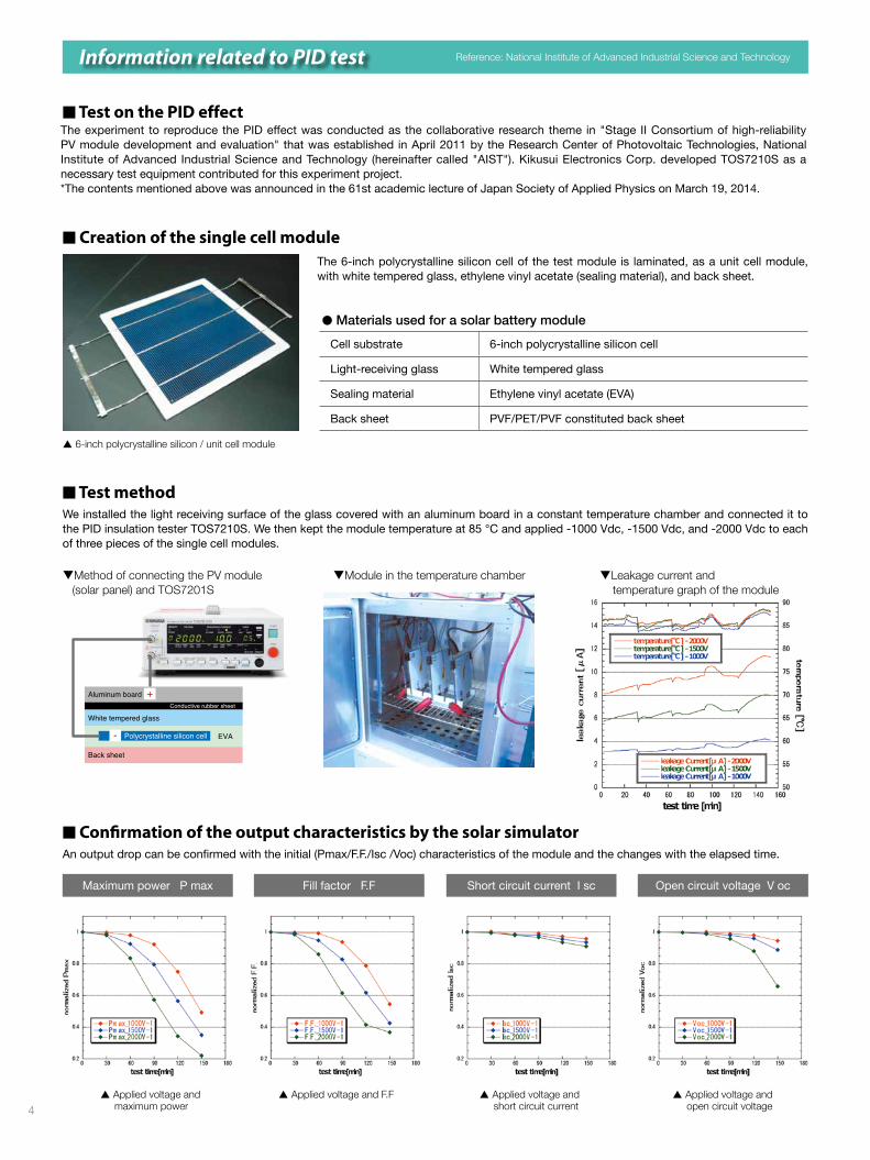
n Test methodWe installed the light receiving surface of the glass covered with an aluminum board in a constant temperature chamber and connected it to the PID insulation tester TOS7210S. We then kept the module temperature at 85 and applied -1000 Vdc, -1500 Vdc, and -2000 Vdc to each of three pieces of the single cell modules.
n Confirmation of the output characteristics by the solar simulatorAn output drop can be confirmed with the initial (Pmax/F.F./Isc /Voc) characteristics of the module and the changes with the elapsed time.
p 6-inch polycrystalline silicon / unit cell module
The 6-inch polycrystalline silicon cell of the test module is laminated, as a unit cell module, with white tempered glass, ethylene vinyl acetate (sealing material), and back sheet.
qModule in the temperature chamberqMethod of connecting the PV module (solar panel) and TOS7201S
qLeakage current and temperature graph of the module
p Applied voltage and maximum power
p Applied voltage and F.F p Applied voltage and short circuit current
p Applied voltage and open circuit voltage
n Creation of the single cell module
The experiment to reproduce the PID effect was conducted as the collaborative research theme in "Stage II Consortium of high-reliability PV module development and evaluation" that was established in April 2011 by the Research Center of Photovoltaic Technologies, National Institute of Advanced Industrial Science and Technology (hereinafter called "AIST"). Kikusui Electronics Corp. developed TOS7210S as a necessary test equipment contributed for this experiment project.*The contents mentioned above was announced in the 61st academic lecture of Japan Society of Applied Physics on March 19, 2014.
n Test on the PID effect
Maximum power P max Fill factor F.F Short circuit current I sc Open circuit voltage V oc
l Materials used for a solar battery moduleCell substrate 6-inch polycrystalline silicon cell
Light-receiving glass White tempered glass
Sealing material Ethylene vinyl acetate (EVA)
Back sheet PVF/PET/PVF constituted back sheet
Reference: National Institute of Advanced Industrial Science and Technology
+
Back sheet
- Polycrystalline silicon cell EVA
White tempered glass
Aluminum boardConductive rubber sheet

5
The normal part emits light perfectly, but as the deterioration accelerates, the shaded area increases eventually and ceases to emit light. This method is adopted useful to confirm the PID effect. In addition, it is admitted that the deterioration in the PID effect is reduced with the elapled time by a reversible effect or recovered nearly to the initial state.
n Confirmation of the deterioration by EL (electro-luminescence)
n Various evaluation methodsUnder the present conditions, any of the evaluation test method or the standard are not established. Each of the research organizations, experiment stations, and module manufacturers in the various countries conducting its own evaluation.l Water method : Method to apply the water on the module glass surface and apply the voltagel Chamber method : Method to manage temperature and humidity in the temperature chamber and apply the voltagel Aluminum method : Method to cover the glass with an aluminum foil or let an aluminum board adhere to the glass surface, and apply the voltageWe continue experiments in each test method to examine each superiority and inferiority, difference by the temperature or humidity for future standardization. The international standard IEC is devising the test method for the PID effect.
n Confirm the difference in deterioration by applied voltageThe ratio that the maximum electricity (Pmax) of the module decreases when the applied voltage increases.In addition, as the EL image indicates, the higher the applied voltage becomes, the shaded area in the EL image increases in the same interval.
In the PID effect after conducting the reversible effect test, it may be found that the deterioration is reduced or recover nearly to the initial state in some module by being left or the reverse voltage is being applied. The polarity can be easily changed in TOS7210S with the switch. You are not bothered by the complicated connection to the DUT. The module that the Pmax drops remarkably (less than -99 %), and the recovery is not confirmed even after applying voltage for long hours. On the other hand, the module that the Pmax drops moderately (approximately -53 % to -71 %) recovered almost perfectly in 0.5 to two hours. In addition, it canbe recovered regardless of the applied voltage.
Deteriorated Deteriorated
Normal Normal (recovered)
Reversible effect (exposed indoor)Result of EL test
Reference: National Institute of Advanced Industrial Science and Technology
n Recovery examination and the results by applying the reverse voltageqRecovery of the sample that output drops by -99 % and less in the PID experiment
+1000 V +1500 V +2000 V
qRecovery of the sample that output drops by -65 % to -71 % and less in the PID experiment
+1000 V +1500 V +2000 V
qRecovery of the sample that output drops by -53 % to -58 % and less in the PID experiment
+1000 V +1500 V +2000 V Result of EL test after recovery test
-99 % and less
200 hours later
-65 to -71 %
2 hours later
-53 to -58 %
2 hours later
Output lowered
Information related to PID test

Output sectionOutput voltage range 50 V to 2000 V
Resolution 1 VAccuracy ± (1.5 % of setting + 2 V)
Maximum rated output 2 W (2000 V/1 mA)Maximum rated current 1 mAOutput terminals
Output type Floating
Isolation voltage ± 1000 Vdc (The terminal that polarity is set to positive polarity)+ 1000 Vdc and -3000 Vdc (The terminal that polarity is set to negative polarity)
Ripple 2000 V/under no load 10 Vp-p or lessMaximum rated load 10 Vp-p or less
Voltage regulation 1 % or less (Maximum rated load gNo load)Short-circuiting current 2 mA or less (Instant 200 mA or less)Output rise time 50 ms or less (10 % to 90 %, no load)Discharge function Forced discharge at the end of test (discharge resistance: 20 kΩ)
VoltmeterMeasurement range 0 V to 2400 VResolution 1 VAccuracy ± (1 % of reading +1 V)
Resistance meterMeasurement range 0.01 MΩ to 5000 MΩ (In the range of over 100 nA to a maximum rated current of 1 mA)Display c.cc MΩ [R < 10.0 MΩ]
cc.c MΩ [10.0 MΩ ≤ R < 100.0 MΩ]ccc MΩ [100.0 MΩ ≤ R < 1000 MΩ]cccc MΩ [1000 MΩ ≤ R ≤ 5000 MΩ](R = measured insulation resistance)
Accuracy *1 ± (10 % of reading) [100 nA < i ≤ 200 nA]± (5 % of reading) [200nA < i ≤ 1 μA]±(2 % of reading) [1 μA < i ≤ 1 mA]( i= measured output-voltage value/measured resistance value)
Measurement range The current measurement range is selectable between AUTO and FIX.
AUTO Automatically changes the current measurement rangeaccording to the measured current value.
FIX Fixes the current measurement range based on the output voltage set valueand LOWER set value (in UPPER OFF status).
Holding function Holds the resistance value obtained at the end of testing while a PASS judgment is being output.Ammeter
Measurement range 0.000 μA to 1900 μADisplay c.ccc μA [i < 10.00 μA]
cc.cc μA [10.00 μA ≤ i < 100.0 μA]ccc.c μA [100.0 μA ≤ i < 1000 μA]cccc μA [1000 μA ≤ i]( i= measured current value)
Accuracy *2 ±(4% of reading +0.005 μA) [i < 10.00 μA]±(4% of reading +0.005 μA) [10.00 μA ≤ i < 100.0 μA]±(2% of reading +0.005 μA) [100.0 μA ≤ i < 1000 μA]±(2% of reading) [1000 μA ≤ i]( i= measured current value)
Measurement range The current measurement range is selectable between AUTO and FIX.AUTO Automatically changes the current measurement range according to the measured current value.
FIX Fixes the current measurement range based on the output voltage set valueand LOWER set value (in UPPER OFF status).
Judgment function
Judgement method/action
UPPER FAIL Judgement If a resistance value equal or less than the lower resistance is detected,the tester shuts off the output and returns an UPPER FAIL judgment.
LOWER FAIL JudgementIf a resistance value equal or less than the lower resistance is detected,the tester shuts off the output and returns a LOWER FAIL judgment.Note that no judgment is made within the judgment wait time (WAIT TIME) after the start of the test.
TimeSetting range for the test duration 0.5 s to 999 s (Consecutive operation by setting TEST TIME as OFF)Setting range for the wait time 0.3 s to 10 s (TEST TIME > WAIT TIME)Accuracy ±(100 ppm + 20 ms)
/Specifications
6

SIGNAL I/O D-SUB 25-pin connector on the rear panelInputspecifications
High-level input voltage 11 V to 15 VAll input signals are active Low controlled.The input terminal is pulled up to +12 V using a resistor.Opening the input terminal is equivalent to inputting a high-level signal.
Low-level input voltage 0 V to 4 VLow-level input current -5 mA maximumInput time width 5 ms minimum
Outputspecifications
Output method Open collector output (4.5 Vdc to 30 Vdc)Output withstand voltage 30 VdcOutput saturation voltage Approx. 1.1 V (at 25°C)Maximum output current 400 mA (TOTAL)
ANALOG OUT Outputs the measured resistance, measured current and voltage, and current range in DC voltage.Measured resistance V0 = log
Rx: (1 MΩ: 0.3 V, 10 MΩ: 1.04 V, 100 MΩ: 2.00 V, 1000 MΩ: 3.00 V, 10000 MΩ or more: 4.00 V)Output impedance: 1 kΩ
Measured current Renge1: V0 [V]= measured value [μA]/ 512 Renge3: V0 [V]= measured value [μA]/8Renge2: V0 [V]= measured value [μA]/64 Renge4: V0 [V]= measured value [μA]
COM Analog output-circuit commonAccuracy ±(2 % of full scale)
RS232C D-SUB 9-pin connector on the rear panel (compliant with EIA-232-D)All functions other than the POWER switch and KEY-LOCK
Baud rate 9600 bps/19200 bps/38400 bps (data: 8 bits; parity: none; stop bit: 2 bits fixed)REMOTE 6-pin mini-DIN connector on the front panel
The optional remote controller RC01-TOS or RC02-TOS is connected to control remotelystarting/stopping of a test (note that a DIN-mini DIN adapter is required).
Display 7-segment LED, 4-digit voltage display, 4-digit insulation resistance display,4-digit current display, and 3-digit time display
Memory function A maximum of 10 types of test conditions can be stored in memoryTEST MODE MOMENTARY A test is conducted only when the START switch is pressed.
FAIL MODE Disables cancellation of FAIL judgment using a stop signal via remote control.
DOUBLE ACTION Starts a test only when the STOP switch is pressed and the START switch ispressed within approximately a half-second.
PASS HOLD Allows the time of holding PASS judgment to be set to 0.2 s or HOLDKEYLOCK Places the tester in a state in which no keystroke other than the START/STOP switch is acceptedEnvironment
Installation location Indoors and at altitudes up to 2000 mWarranty range Temperature/Humidity 15 °C to 30 °C/20 % rh to 80 % rh (no condensation)Operating range Temperature/Humidity 0 °C to 40 °C/20 % rh to 80 % rh (no condensation)Storage range Temperature/Humidity -20 °C to 70 °C/90 % rh or less (no condensation)
Power requirementsNominal voltage range(allowable voltage range) 100 Vac to 240 Vac (85 Vac to 250 Vac)Power consumption At rated load 30 VA maximumAllowable frequency range 47 Hz to 63 Hz
Insulation resistance 30 MΩ or more (500 Vdc) (AC LINE to chassis)Hipot 1500 Vac for 1 second, 10 mA or less (AC LINE to chassis), 3000 V AC for 1 second (A, B terminals to chassis)Ground bond 25 Aac/0.1 Ω or lessDimensions (mm (inch)) (maximum dimensions) /Weight
214 (8.43") W × 81(3.19") (115 (4.53")) H × 340 (13.39") (385 (15.16")) D/Approx. 2 kg (Approx.4.41 lbs)
*1. Humidity: 20 %rh to 70 %rh (no condensation). No bends in the test leads.*2. Humidity: 20 %rh to 80 %rh (no condensation). No bends in the test leads. Humidity 20 %rh to 70 %rh when either of terminal A or terminal B is grounded (no condensation). No bends in the test leads.
/Specifications
l Rear panel l Accessories: Shielded cable
1 +( )R X
1M
7

Printed in Japan Issue:Sep.2014 2014091KPRIEC11
n All products contained in this catalogue are equipment and devices that are premised on use under the supervision of qualified personnel, and are not designed or produced for home-use or use by general consumers. n Specifications, design and so forth are subject to change without prior notice to improve the quality. n Product names and prices are subject to change and production may be discontinued when necessary. n Product names, company names and brand names contained in this catalogue represent the respective registered trade name or trade mark. n Colors, textures and so forth of photographs shown in this catalogue may differ from actual products due to a limited fidelity in printing. n Although every effort has been made to provide the information as accurate as possible for this catalogue, certain details have unavoidably been omitted due to limitations in space. n If you find any misprints or errors in this catalogue, it would be appreciated if you would inform us. n Please contact our distributors to confirm specifications, price, accessories or anything that may be unclear when placing an order or concluding a purchasing agreement.
lDistributor/Representative
www.kikusui.cnRoom 216,Building 4, No.641,Tianshan Road, Shanghai City, China Phone : 021-5887-9067 Facsimile : 021-5887-9069
2975 Bowers Avenue, Suite 307, Santa Clara, CA 95051Phone : 408-980-9433 Facsimile : 408-980-9409
www.kikusuiamerica.com1-877-876-2807