Embed Size (px)
Citation preview

2012-2017 Microchip Technology Inc. DS60001185G-page 1
PIC32MX330/350/370/430/450/470
Operating Conditions: 2.3V to 3.6V• -40ºC to +105ºC (DC to 80 MHz)• -40ºC to +85ºC (DC to 100 MHz)• 0ºC to +70ºC (DC to 120 MHz)
Core: 120 MHz/150 DMIPS MIPS32® M4K®
• MIPS16e® mode for up to 40% smaller code size• Code-efficient (C and Assembly) architecture• Single-cycle (MAC) 32x16 and two-cycle 32x32 multiply
Clock Management• 0.9% internal oscillator• Programmable PLLs and oscillator clock sources• Fail-Safe Clock Monitor (FSCM)• Independent Watchdog Timer• Fast wake-up and start-up
Power Management• Low-power management modes (Sleep and Idle)• Integrated Power-on Reset, Brown-out Reset, and High
Voltage Detect• 0.5 mA/MHz dynamic current (typical)• 50 μA IPD current (typical)
Audio/Graphics/Touch HMI Features• External graphics interface with up to 34 PMP pins• Audio data communication: I2S, LJ, RJ, USB• Audio data control interface: SPI and I2C• Audio data master clock:
- Generation of fractional clock frequencies- Can be synchronized with USB clock- Can be tuned in run-time
• Charge Time Measurement Unit (CTMU):- Supports mTouch™ capacitive touch sensing- Provides high-resolution time measurement (1 ns)
Advanced Analog Features• ADC Module:
- 10-bit 1 Msps rate with one Sample and Hold (S&H)- Up to 28 analog inputs- Can operate during Sleep mode
• Flexible and independent ADC trigger sources• On-chip temperature measurement capability• Comparators:
- Two dual-input Comparator modules- Programmable references with 32 voltage points
Timers/Output Compare/Input Capture• Five General Purpose Timers:
- Five 16-bit and up to two 32-bit Timers/Counters• Five Output Compare (OC) modules• Five Input Capture (IC) modules• Peripheral Pin Select (PPS) to allow function remap• Real-Time Clock and Calendar (RTCC) module
Communication Interfaces• USB 2.0-compliant Full-speed OTG controller• Up to five UART modules (20 Mbps):
- LIN 2.1 protocols and IrDA® support• Two 4-wire SPI modules (25 Mbps)• Two I2C modules (up to 1 Mbaud) with SMBus support• PPS to allow function remap• Parallel Master Port (PMP)
Direct Memory Access (DMA)• Four channels of hardware DMA with automatic data
size detection• 32-bit Programmable Cyclic Redundancy Check (CRC)• Two additional channels dedicated to USB
Input/Output• 15 mA or 12 mA source/sink for standard VOH/VOL and
up to 22 mA for non-standard VOH1• 5V-tolerant pins• Selectable open drain, pull-ups, and pull-downs• External interrupts on all I/O pins
Qualification and Class B Support• AEC-Q100 REVH (Grade 2 -40ºC to +105ºC) planned• Class B Safety Library, IEC 60730
Debugger Development Support• In-circuit and in-application programming• 4-wire MIPS® Enhanced JTAG interface• Unlimited program and six complex data breakpoints• IEEE 1149.2-compatible (JTAG) boundary scan
Type QFN TQFP VTLA
Pin Count 64 64 100 100 124I/O Pins (up to) 53 53 85 85 85
Contact/Lead Pitch 0.50 0.50 0.40 0.50 0.50Dimensions 9x9x0.9 10x10x1 12x12x1 14x14x1 9x9x0.9
Note: All dimensions are in millimeters (mm) unless specified.
Packages
32-bit Microcontrollers (up to 512 KB Flash and 128 KB SRAM) with Audio/Graphics/Touch (HMI), USB, and Advanced Analog

PIC32MX330/350/370/430/450/470
DS60001185G-page 2 2012-2017 Microchip Technology Inc.
TABLE 1: PIC32MX330/350/370/430/450/470 CONTROLLER FAMILY FEATURES
Dev
ice
Pins
Pack
ages
Prog
ram
Mem
ory
(KB
)(1)
Dat
a M
emor
y (K
B)
Remappable Peripherals
10-b
it 1
Msp
s A
DC
(Cha
nnel
s)
Ana
log
Com
para
tors
USB
On-
The-
Go
(OTG
)
CTM
U
I2 C PMP
RTC
C
DM
A C
hann
els
(Pro
gram
mab
le/D
edic
ated
)
I/O P
ins
JTA
G
Trac
e
Rem
appa
ble
Pins
Tim
ers/
Cap
ture
/Com
pare
(2)
UA
RT
SPI/I
2 S
Exte
rnal
Inte
rrup
ts(3
)
PIC32MX330F064H 64 QFN, TQFP 64+12 16 37 5/5/5 4 2/2 5 28 2 N Y 2 Y Y 4/0 53 Y N
PIC32MX330F064L100 TQFP
64+12 16 54 5/5/5 5 2/2 5 28 2 N Y 2 Y Y 4/0 85 Y Y124 VTLA
PIC32MX350F128H 64 QFN, TQFP 128+12 32 37 5/5/5 4 2/2 5 28 2 N Y 2 Y Y 4/0 53 Y N
PIC32MX350F128L100 TQFP
128+12 32 54 5/5/5 5 2/2 5 28 2 N Y 2 Y Y 4/0 85 Y Y124 VTLA
PIC32MX350F256H 64 QFN, TQFP 256+12 64 37 5/5/5 4 2/2 5 28 2 N Y 2 Y Y 4/0 53 Y N
PIC32MX350F256L100 TQFP
256+12 64 54 5/5/5 5 2/2 5 28 2 N Y 2 Y Y 4/0 85 Y Y124 VTLA
PIC32MX370F512H 64 QFN, TQFP 512+12 128 37 5/5/5 4 2/2 5 28 2 N Y 2 Y Y 4/0 53 Y N
PIC32MX370F512L100 TQFP
512+12 128 54 5/5/5 5 2/2 5 28 2 N Y 2 Y Y 4/0 85 Y Y124 VTLA
PIC32MX430F064H 64 QFN, TQFP 64+12 16 34 5/5/5 4 2/2 5 28 2 Y Y 2 Y Y 4/2 49 Y N
PIC32MX430F064L100 TQFP
64+12 16 51 5/5/5 5 2/2 5 28 2 Y Y 2 Y Y 4/2 81 Y Y124 VTLA
PIC32MX450F128H 64 QFN, TQFP 128+12 32 34 5/5/5 4 2/2 5 28 2 Y Y 2 Y Y 4/2 49 Y N
PIC32MX450F128L100 TQFP
128+12 32 51 5/5/5 5 2/2 5 28 2 Y Y 2 Y Y 4/2 81 Y Y124 VTLA
PIC32MX450F256H 64 QFN, TQFP 256+12 64 34 5/5/5 4 2/2 5 28 2 Y Y 2 Y Y 4/2 49 Y N
PIC32MX450F256L100 TQFP
256+12 64 51 5/5/5 5 2/2 5 28 2 Y Y 2 Y Y 4/2 81 Y Y124 VTLA
PIC32MX470F512H 64 QFN, TQFP 512+12 128 34 5/5/5 4 2/2 5 28 2 Y Y 2 Y Y 4/2 49 Y N
PIC32MX470F512L100 TQFP
512+12 128 51 5/5/5 5 2/2 5 28 2 Y Y 2 Y Y 4/2 81 Y Y124 VTLA
Note 1: All devices feature 12 KB of Boot Flash memory.2: Four out of five timers are remappable.3: Four out of five external interrupts are remappable.

2012-2017 Microchip Technology Inc. DS60001185G-page 3
PIC32MX330/350/370/430/450/470Device Pin Tables
TABLE 2: PIN NAMES FOR 64-PIN DEVICES
Pin # Full Pin Name Pin # Full Pin Name
1 AN22/RPE5/PMD5/RE5 33 RPF3/RF3
2 AN23/PMD6/RE6 34 RPF2/RF2
3 AN27/PMD7/RE7 35 RPF6/SCK1/INT0/RF6
4 AN16/C1IND/RPG6/SCK2/PMA5/RG6 36 SDA1/RG3
5 AN17/C1INC/RPG7/PMA4/RG7 37 SCL1/RG2
6 AN18/C2IND/RPG8/PMA3/RG8 38 VDD
7 MCLR 39 OSC1/CLKI/RC12
8 AN19/C2INC/RPG9/PMA2/RG9 40 OSC2/CLKO/RC15
9 VSS 41 VSS
10 VDD 42 RPD8/RTCC/RD8
11 AN5/C1INA/RPB5/RB5 43 RPD9/RD9
12 AN4/C1INB/RB4 44 RPD10/PMCS2/RD10
13 PGED3/AN3/C2INA/RPB3/RB3 45 RPD11/PMCS1/RD11
14 PGEC3/AN2/C2INB/RPB2/CTED13/RB2 46 RPD0/RD0
15 PGEC1/VREF-/CVREF-/AN1/RPB1/CTED12/RB1 47 SOSCI/RPC13/RC13
16 PGED1/VREF+/CVREF+/AN0/RPB0/PMA6/RB0 48 SOSCO/RPC14/T1CK/RC14
17 PGEC2/AN6/RPB6/RB6 49 AN24/RPD1/RD1
18 PGED2/AN7/RPB7/CTED3//RB7 50 AN25/RPD2/RD2
19 AVDD 51 AN26/RPD3/RD3
20 AVSS 52 RPD4/PMWR/RD4
21 AN8/RPB8/CTED10//RB8 53 RPD5/PMRD/RD5
22 AN9/RPB9/CTED4/PMA7/RB9 54 RD6
23 TMS/CVREFOUT/AN10/RPB10/CTED11//PMA13/RB10 55 RD7
24 TDO/AN11/PMA12/RB11 56 VCAP
25 VSS 57 VDD
26 VDD 58 RPF0/RF0
27 TCK/AN12/PMA11/RB12 59 RPF1/RF1
28 TDI/AN13/PMA10/RB13 60 PMD0/RE0
29 AN14/RPB14/CTED5/PMA1/RB14 61 PMD1/RE1
30 AN15/RPB15/OCFB/CTED6/PMA0/RB15 62 AN20/PMD2/RE2
31 RPF4/SDA2/PMA9/RF4 63 RPE3/CTPLS/PMD3/RE3
32 RPF5/SCL2/PMA8/RF5 64 AN21/PMD4/RE4
Note 1: The RPn pins can be used by remappable peripherals. See Table 1 for the available peripherals and Section 12.3 “Peripheral Pin Select” for restrictions.
2: Every I/O port pin (RBx-RGx), with the exception of RF6, can be used as a change notification pin (CNBx-CNGx). See Section 12.0 “I/O Ports” for more information.
3: The metal plane at the bottom of the device is not connected to any pins and is recommended to be connected to VSS externally.4: RPF6 (pin 35) is only available for output functions.
64-PIN QFN(1,2,3,4) AND TQFP(1,2,3,4) (TOP VIEW)
PIC32MX330F064HPIC32MX350F128H
PIC32MX370F512H64 1
QFN(4)
PIC32MX350F256H
164
TQFP
PIC32MX330/350/370/430/450/470
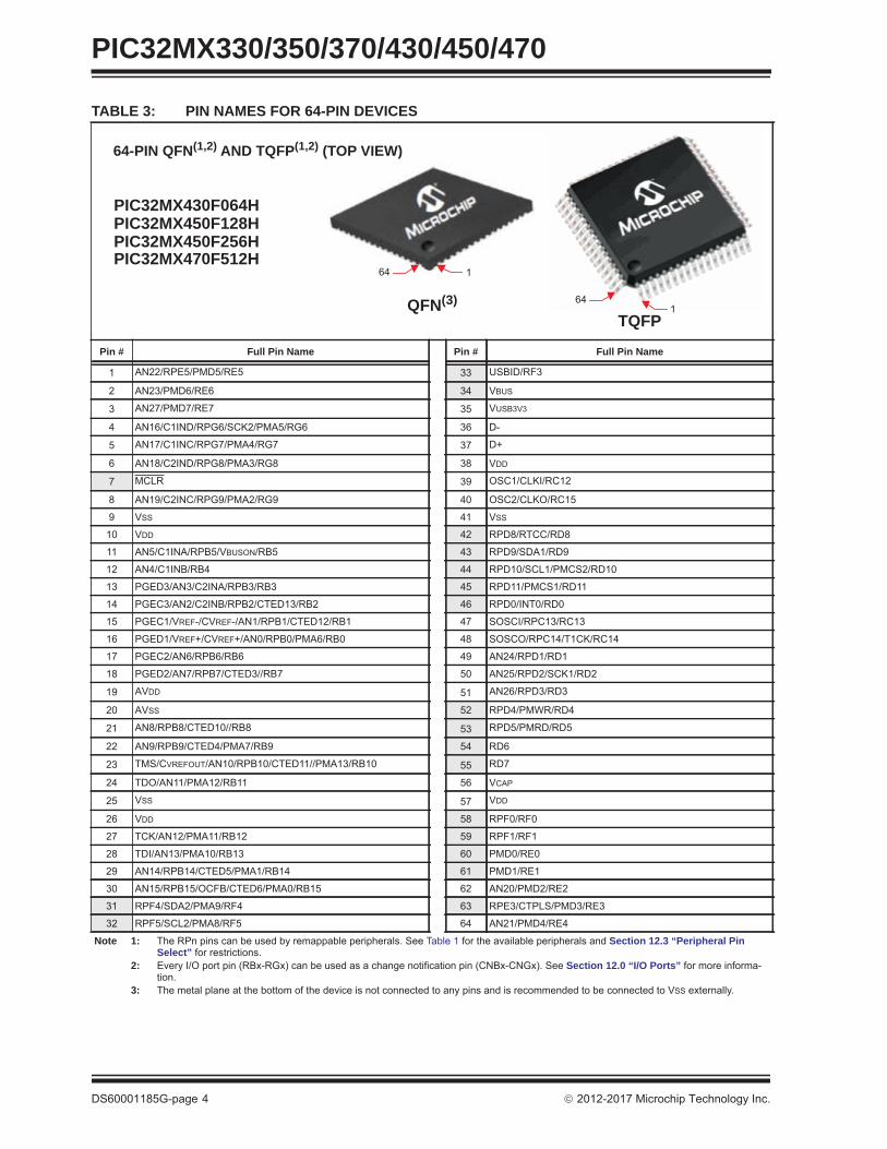
DS60001185G-page 4 2012-2017 Microchip Technology Inc.
TABLE 3: PIN NAMES FOR 64-PIN DEVICES
Pin # Full Pin Name Pin # Full Pin Name
1 AN22/RPE5/PMD5/RE5 33 USBID/RF3
2 AN23/PMD6/RE6 34 VBUS
3 AN27/PMD7/RE7 35 VUSB3V3
4 AN16/C1IND/RPG6/SCK2/PMA5/RG6 36 D-
5 AN17/C1INC/RPG7/PMA4/RG7 37 D+
6 AN18/C2IND/RPG8/PMA3/RG8 38 VDD
7 MCLR 39 OSC1/CLKI/RC12
8 AN19/C2INC/RPG9/PMA2/RG9 40 OSC2/CLKO/RC15
9 VSS 41 VSS
10 VDD 42 RPD8/RTCC/RD8
11 AN5/C1INA/RPB5/VBUSON/RB5 43 RPD9/SDA1/RD9
12 AN4/C1INB/RB4 44 RPD10/SCL1/PMCS2/RD10
13 PGED3/AN3/C2INA/RPB3/RB3 45 RPD11/PMCS1/RD11
14 PGEC3/AN2/C2INB/RPB2/CTED13/RB2 46 RPD0/INT0/RD0
15 PGEC1/VREF-/CVREF-/AN1/RPB1/CTED12/RB1 47 SOSCI/RPC13/RC13
16 PGED1/VREF+/CVREF+/AN0/RPB0/PMA6/RB0 48 SOSCO/RPC14/T1CK/RC14
17 PGEC2/AN6/RPB6/RB6 49 AN24/RPD1/RD1
18 PGED2/AN7/RPB7/CTED3//RB7 50 AN25/RPD2/SCK1/RD2
19 AVDD 51 AN26/RPD3/RD3
20 AVSS 52 RPD4/PMWR/RD4
21 AN8/RPB8/CTED10//RB8 53 RPD5/PMRD/RD5
22 AN9/RPB9/CTED4/PMA7/RB9 54 RD6
23 TMS/CVREFOUT/AN10/RPB10/CTED11//PMA13/RB10 55 RD7
24 TDO/AN11/PMA12/RB11 56 VCAP
25 VSS 57 VDD
26 VDD 58 RPF0/RF0
27 TCK/AN12/PMA11/RB12 59 RPF1/RF1
28 TDI/AN13/PMA10/RB13 60 PMD0/RE0
29 AN14/RPB14/CTED5/PMA1/RB14 61 PMD1/RE1
30 AN15/RPB15/OCFB/CTED6/PMA0/RB15 62 AN20/PMD2/RE2
31 RPF4/SDA2/PMA9/RF4 63 RPE3/CTPLS/PMD3/RE3
32 RPF5/SCL2/PMA8/RF5 64 AN21/PMD4/RE4
Note 1: The RPn pins can be used by remappable peripherals. See Table 1 for the available peripherals and Section 12.3 “Peripheral Pin Select” for restrictions.
2: Every I/O port pin (RBx-RGx) can be used as a change notification pin (CNBx-CNGx). See Section 12.0 “I/O Ports” for more informa-tion.
3: The metal plane at the bottom of the device is not connected to any pins and is recommended to be connected to VSS externally.
64 1
QFN(3)1
64
TQFP
64-PIN QFN(1,2) AND TQFP(1,2) (TOP VIEW)
PIC32MX430F064HPIC32MX450F128H
PIC32MX470F512HPIC32MX450F256H

2012-2017 Microchip Technology Inc. DS60001185G-page 5
PIC32MX330/350/370/430/450/470
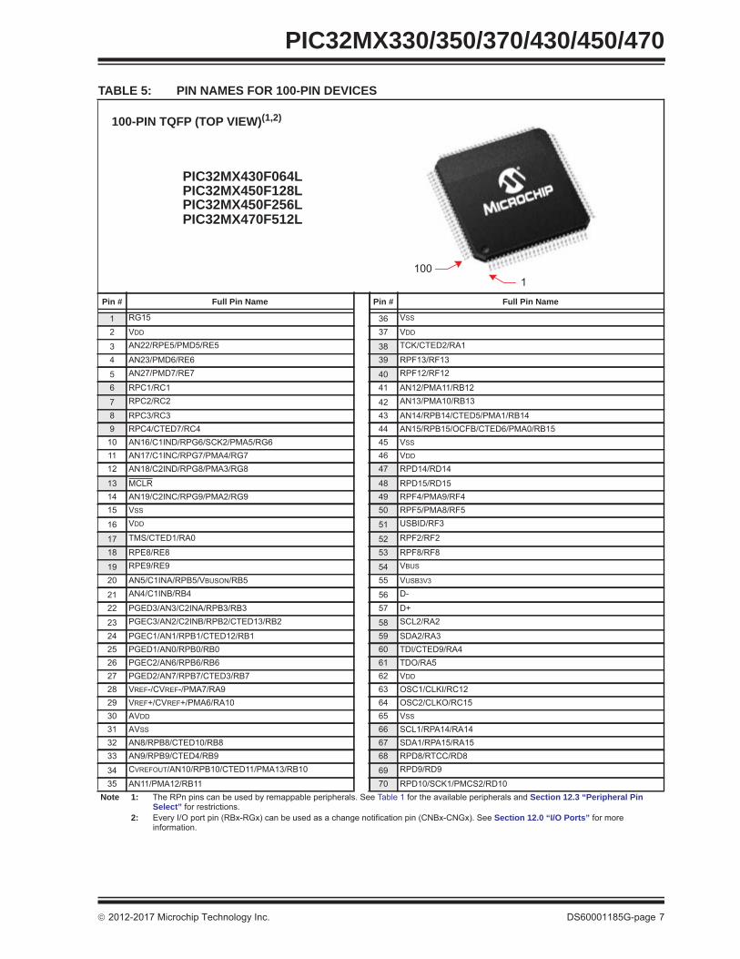
TABLE 4: PIN NAMES FOR 100-PIN DEVICES
Pin # Full Pin Name Pin # Full Pin Name
1 RG15 36 VSS
2 VDD 37 VDD
3 AN22/RPE5/PMD5/RE5 38 TCK/CTED2/RA1
4 AN23/PMD6/RE6 39 RPF13/RF13
5 AN27/PMD7/RE7 40 RPF12/RF12
6 RPC1/RC1 41 AN12/PMA11/RB12
7 RPC2/RC2 42 AN13/PMA10/RB13
8 RPC3/RC3 43 AN14/RPB14/CTED5/PMA1/RB149 RPC4/CTED7/RC4 44 AN15/RPB15/OCFB/CTED6/PMA0/RB15
10 AN16/C1IND/RPG6/SCK2/PMA5/RG6 45 VSS
11 AN17/C1INC/RPG7/PMA4/RG7 46 VDD
12 AN18/C2IND/RPG8/PMA3/RG8 47 RPD14/RD14
13 MCLR 48 RPD15/RD1514 AN19/C2INC/RPG9/PMA2/RG9 49 RPF4/PMA9/RF415 VSS 50 RPF5/PMA8/RF5
16 VDD 51 RPF3/RF3
17 TMS/CTED1/RA0 52 RPF2/RF2
18 RPE8/RE8 53 RPF8/RF8
19 RPE9/RE9 54 RPF7/RF7
20 AN5/C1INA/RPB5/RB5 55 RPF6/SCK1/INT0/RF6
21 AN4/C1INB/RB4 56 SDA1/RG3
22 PGED3/AN3/C2INA/RPB3/RB3 57 SCL1/RG2
23 PGEC3/AN2/C2INB/RPB2/CTED13/RB2 58 SCL2/RA2
24 PGEC1/AN1/RPB1/CTED12/RB1 59 SDA2/RA325 PGED1/AN0/RPB0/RB0 60 TDI/CTED9/RA426 PGEC2/AN6/RPB6/RB6 61 TDO/RA527 PGED2/AN7/RPB7/CTED3/RB7 62 VDD
28 VREF-/CVREF-/PMA7/RA9 63 OSC1/CLKI/RC1229 VREF+/CVREF+/PMA6/RA10 64 OSC2/CLKO/RC1530 AVDD 65 VSS
31 AVSS 66 RPA14/RA1432 AN8/RPB8/CTED10/RB8 67 RPA15/RA1533 AN9/RPB9/CTED4/RB9 68 RPD8/RTCC/RD8
34 CVREFOUT/AN10/RPB10/CTED11PMA13/RB10 69 RPD9/RD9
35 AN11/PMA12/RB11 70 RPD10/PMCS2/RD10Note 1: The RPn pins can be used by remappable peripherals. See Table 1 for the available peripherals and Section 12.3 “Peripheral Pin
Select” for restrictions.2: Every I/O port pin (RAx-RGx), with the exception of RF6, can be used as a change notification pin (CNAx-CNGx). See Section 12.0 “I/O
Ports” for more information.3: RPF6 (pin 55) and RPF7 (pin 54) are only remappable for input functions.
1100
100-PIN TQFP (TOP VIEW)(1,2,3)
PIC32MX330F064LPIC32MX350F128L
PIC32MX370F512LPIC32MX350F256L

PIC32MX330/350/370/430/450/470
DS60001185G-page 6 2012-2017 Microchip Technology Inc.
71 RPD11/PMCS1/RD11 86 VDD
72 RPD0/RD0 87 RPF0/PMD11/RF0
73 SOSCI/RPC13/RC13 88 RPF1/PMD10/RF1
74 SOSCO/RPC14/T1CK/RC14 89 RPG1/PMD9/RG1
75 VSS 90 RPG0/PMD8/RG0
76 AN24/RPD1/RD1 91 TRCLK/RA677 AN25/RPD2/RD2 92 TRD3/CTED8/RA778 AN26/RPD3/RD3 93 PMD0/RE079 RPD12/PMD12/RD12 94 PMD1/RE180 PMD13/RD13 95 TRD2/RG1481 RPD4/PMWR/RD4 96 TRD1/RG12
82 RPD5/PMRD/RD5 97 TRD0/RG13
83 PMD14/RD6 98 AN20/PMD2/RE284 PMD15/RD7 99 RPE3/CTPLS/PMD3/RE385 VCAP 100 AN21/PMD4/RE4
TABLE 4: PIN NAMES FOR 100-PIN DEVICES (CONTINUED)
Pin # Full Pin Name Pin # Full Pin Name
Note 1: The RPn pins can be used by remappable peripherals. See Table 1 for the available peripherals and Section 12.3 “Peripheral Pin Select” for restrictions.
2: Every I/O port pin (RAx-RGx), with the exception of RF6, can be used as a change notification pin (CNAx-CNGx). See Section 12.0 “I/O Ports” for more information.
3: RPF6 (pin 55) and RPF7 (pin 54) are only remappable for input functions.
1100
100-PIN TQFP (TOP VIEW)(1,2,3)
PIC32MX330F064LPIC32MX350F128L
PIC32MX370F512LPIC32MX350F256L
2012-2017 Microchip Technology Inc. DS60001185G-page 7
PIC32MX330/350/370/430/450/470
TABLE 5: PIN NAMES FOR 100-PIN DEVICES
Pin # Full Pin Name Pin # Full Pin Name
1 RG15 36 VSS
2 VDD 37 VDD
3 AN22/RPE5/PMD5/RE5 38 TCK/CTED2/RA1
4 AN23/PMD6/RE6 39 RPF13/RF13
5 AN27/PMD7/RE7 40 RPF12/RF12
6 RPC1/RC1 41 AN12/PMA11/RB12
7 RPC2/RC2 42 AN13/PMA10/RB13
8 RPC3/RC3 43 AN14/RPB14/CTED5/PMA1/RB149 RPC4/CTED7/RC4 44 AN15/RPB15/OCFB/CTED6/PMA0/RB15
10 AN16/C1IND/RPG6/SCK2/PMA5/RG6 45 VSS
11 AN17/C1INC/RPG7/PMA4/RG7 46 VDD
12 AN18/C2IND/RPG8/PMA3/RG8 47 RPD14/RD14
13 MCLR 48 RPD15/RD1514 AN19/C2INC/RPG9/PMA2/RG9 49 RPF4/PMA9/RF415 VSS 50 RPF5/PMA8/RF5
16 VDD 51 USBID/RF3
17 TMS/CTED1/RA0 52 RPF2/RF2
18 RPE8/RE8 53 RPF8/RF8
19 RPE9/RE9 54 VBUS
20 AN5/C1INA/RPB5/VBUSON/RB5 55 VUSB3V3
21 AN4/C1INB/RB4 56 D-
22 PGED3/AN3/C2INA/RPB3/RB3 57 D+
23 PGEC3/AN2/C2INB/RPB2/CTED13/RB2 58 SCL2/RA2
24 PGEC1/AN1/RPB1/CTED12/RB1 59 SDA2/RA325 PGED1/AN0/RPB0/RB0 60 TDI/CTED9/RA426 PGEC2/AN6/RPB6/RB6 61 TDO/RA527 PGED2/AN7/RPB7/CTED3/RB7 62 VDD
28 VREF-/CVREF-/PMA7/RA9 63 OSC1/CLKI/RC1229 VREF+/CVREF+/PMA6/RA10 64 OSC2/CLKO/RC1530 AVDD 65 VSS
31 AVSS 66 SCL1/RPA14/RA1432 AN8/RPB8/CTED10/RB8 67 SDA1/RPA15/RA1533 AN9/RPB9/CTED4/RB9 68 RPD8/RTCC/RD8
34 CVREFOUT/AN10/RPB10/CTED11/PMA13/RB10 69 RPD9/RD9
35 AN11/PMA12/RB11 70 RPD10/SCK1/PMCS2/RD10Note 1: The RPn pins can be used by remappable peripherals. See Table 1 for the available peripherals and Section 12.3 “Peripheral Pin
Select” for restrictions.2: Every I/O port pin (RBx-RGx) can be used as a change notification pin (CNBx-CNGx). See Section 12.0 “I/O Ports” for more
information.
1100
100-PIN TQFP (TOP VIEW)(1,2)
PIC32MX430F064LPIC32MX450F128L
PIC32MX470F512LPIC32MX450F256L

PIC32MX330/350/370/430/450/470
DS60001185G-page 8 2012-2017 Microchip Technology Inc.
71 RPD11/PMCS1/RD11 86 VDD
72 RPD0/INT0/RD0 87 RPF0/PMD11/RF0
73 SOSCI/RPC13/RC13 88 RPF1/PMD10/RF1
74 SOSCO/RPC14/T1CK/RC14 89 RPG1/PMD9/RG1
75 VSS 90 RPG0/PMD8/RG0
76 AN24/RPD1/RD1 91 TRCLK/RA677 AN25/RPD2/RD2 92 TRD3/CTED8/RA778 AN26/RPD3/RD3 93 PMD0/RE079 RPD12/PMD12/RD12 94 PMD1/RE180 PMD13/RD13 95 TRD2/RG1481 RPD4/PMWR/RD4 96 TRD1/RG12
82 RPD5/PMRD/RD5 97 TRD0/RG13
83 PMD14/RD6 98 AN20/CTPLS/PMD2/RE284 PMD15/RD7 99 RPE3/PMD3/RE385 VCAP 100 AN21/PMD4/RE4
TABLE 5: PIN NAMES FOR 100-PIN DEVICES (CONTINUED)
Pin # Full Pin Name Pin # Full Pin Name
Note 1: The RPn pins can be used by remappable peripherals. See Table 1 for the available peripherals and Section 12.3 “Peripheral Pin Select” for restrictions.
2: Every I/O port pin (RBx-RGx) can be used as a change notification pin (CNBx-CNGx). See Section 12.0 “I/O Ports” for more information.
1100
100-PIN TQFP (TOP VIEW)(1,2)
PIC32MX430F064LPIC32MX450F128L
PIC32MX470F512LPIC32MX450F256L
2012-2017 Microchip Technology Inc. DS60001185G-page 9
PIC32MX330/350/370/430/450/470
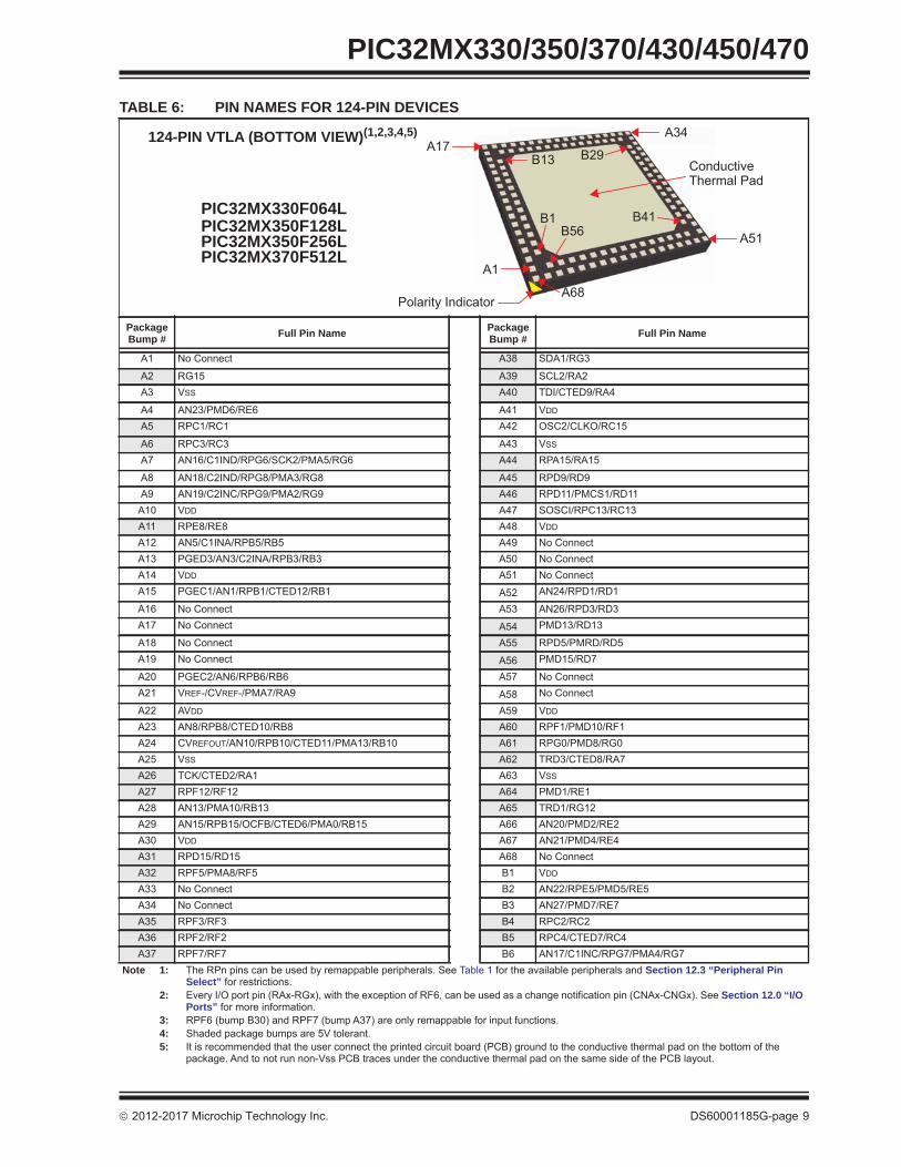
TABLE 6: PIN NAMES FOR 124-PIN DEVICES
Package Bump # Full Pin Name Package
Bump # Full Pin Name
A1 No Connect A38 SDA1/RG3
A2 RG15 A39 SCL2/RA2A3 VSS A40 TDI/CTED9/RA4
A4 AN23/PMD6/RE6 A41 VDD
A5 RPC1/RC1 A42 OSC2/CLKO/RC15
A6 RPC3/RC3 A43 VSS
A7 AN16/C1IND/RPG6/SCK2/PMA5/RG6 A44 RPA15/RA15
A8 AN18/C2IND/RPG8/PMA3/RG8 A45 RPD9/RD9A9 AN19/C2INC/RPG9/PMA2/RG9 A46 RPD11/PMCS1/RD11A10 VDD A47 SOSCI/RPC13/RC13A11 RPE8/RE8 A48 VDD
A12 AN5/C1INA/RPB5/RB5 A49 No ConnectA13 PGED3/AN3/C2INA/RPB3/RB3 A50 No ConnectA14 VDD A51 No ConnectA15 PGEC1/AN1/RPB1/CTED12/RB1 A52 AN24/RPD1/RD1
A16 No Connect A53 AN26/RPD3/RD3A17 No Connect A54 PMD13/RD13
A18 No Connect A55 RPD5/PMRD/RD5A19 No Connect A56 PMD15/RD7
A20 PGEC2/AN6/RPB6/RB6 A57 No ConnectA21 VREF-/CVREF-/PMA7/RA9 A58 No Connect
A22 AVDD A59 VDD
A23 AN8/RPB8/CTED10/RB8 A60 RPF1/PMD10/RF1A24 CVREFOUT/AN10/RPB10/CTED11/PMA13/RB10 A61 RPG0/PMD8/RG0A25 VSS A62 TRD3/CTED8/RA7A26 TCK/CTED2/RA1 A63 VSS
A27 RPF12/RF12 A64 PMD1/RE1A28 AN13/PMA10/RB13 A65 TRD1/RG12A29 AN15/RPB15/OCFB/CTED6/PMA0/RB15 A66 AN20/PMD2/RE2A30 VDD A67 AN21/PMD4/RE4A31 RPD15/RD15 A68 No ConnectA32 RPF5/PMA8/RF5 B1 VDD
A33 No Connect B2 AN22/RPE5/PMD5/RE5A34 No Connect B3 AN27/PMD7/RE7A35 RPF3/RF3 B4 RPC2/RC2A36 RPF2/RF2 B5 RPC4/CTED7/RC4A37 RPF7/RF7 B6 AN17/C1INC/RPG7/PMA4/RG7
Note 1: The RPn pins can be used by remappable peripherals. See Table 1 for the available peripherals and Section 12.3 “Peripheral Pin Select” for restrictions.
2: Every I/O port pin (RAx-RGx), with the exception of RF6, can be used as a change notification pin (CNAx-CNGx). See Section 12.0 “I/O Ports” for more information.
3: RPF6 (bump B30) and RPF7 (bump A37) are only remappable for input functions.4: Shaded package bumps are 5V tolerant.5: It is recommended that the user connect the printed circuit board (PCB) ground to the conductive thermal pad on the bottom of the
package. And to not run non-Vss PCB traces under the conductive thermal pad on the same side of the PCB layout.
A1
A68
A17B29B13
B41B1
A34
A51B56
124-PIN VTLA (BOTTOM VIEW)(1,2,3,4,5)
Polarity Indicator
PIC32MX330F064LPIC32MX350F128L
PIC32MX370F512LPIC32MX350F256L
ConductiveThermal Pad

PIC32MX330/350/370/430/450/470
DS60001185G-page 10 2012-2017 Microchip Technology Inc.
B7 MCLR B32 SDA2/RA3B8 VSS B33 TDO/RA5B9 TMS/CTED1/RA0 B34 OSC1/CLKI/RC12B10 RPE9/RE9 B35 No ConnectB11 AN4/C1INB/RB4 B36 RPA14/RA14B12 VSS B37 RPD8/RTCC/RD8B13 PGEC3/AN2/C2INB/RPB2/CTED13/RB2 B38 RPD10/PMCS2/RD10B14 PGED1/AN0/RPB0/RB0 B39 RPD0/RD0B15 No Connect B40 SOSCO/RPC14/T1CK/RC14B16 PGED2/AN7/RPB7/CTED3/RB7 B41 VSS
B17 VREF+/CVREF+/PMA6/RA10 B42 AN25/RPD2/RD2B18 AVSS B43 RPD12/PMD12/RD12B19 AN9/RPB9/CTED4/RB9 B44 RPD4/PMWR/RD4B20 AN11/PMA12/RB11 B45 PMD14/RD6B21 VDD B46 No Connect
B22 RPF13/RF13 B47 No ConnectB23 AN12/PMA11/RB12 B48 VCAP
B24 AN14/RPB14/CTED5/PMA1/RB14 B49 RPF0/PMD11/RF0
B25 VSS B50 RPG1/PMD9/RG1B26 RPD14/RD14 B51 TRCLK/RA6
B27 RPF4/PMA9/RF4 B52 PMD0/RE0
B28 No Connect B53 VDD
B29 RPF8/RF8 B54 TRD2/RG14B30 RPF6/SCKI/INT0/RF6 B55 TRD0/RG13B31 SCL1/RG2 B56 RPE3/CTPLS/PMD3/RE3
TABLE 6: PIN NAMES FOR 124-PIN DEVICES (CONTINUED)
Package Bump # Full Pin Name Package
Bump # Full Pin Name
Note 1: The RPn pins can be used by remappable peripherals. See Table 1 for the available peripherals and Section 12.3 “Peripheral Pin Select” for restrictions.
2: Every I/O port pin (RAx-RGx), with the exception of RF6, can be used as a change notification pin (CNAx-CNGx). See Section 12.0 “I/O Ports” for more information.
3: RPF6 (bump B30) and RPF7 (bump A37) are only remappable for input functions.4: Shaded package bumps are 5V tolerant.5: It is recommended that the user connect the printed circuit board (PCB) ground to the conductive thermal pad on the bottom of the
package. And to not run non-Vss PCB traces under the conductive thermal pad on the same side of the PCB layout.
A1
A68
A17B29B13
B41B1
A34
A51B56
124-PIN VTLA (BOTTOM VIEW)(1,2,3,4,5)
Polarity Indicator
PIC32MX330F064LPIC32MX350F128L
PIC32MX370F512LPIC32MX350F256L
ConductiveThermal Pad

2012-2017 Microchip Technology Inc. DS60001185G-page 11
PIC32MX330/350/370/430/450/470
TABLE 7: PIN NAMES FOR 124-PIN DEVICES
Package Bump # Full Pin Name Package
Bump # Full Pin Name
A1 No Connect A38 D-
A2 RG15 A39 SCL2/RA2A3 VSS A40 TDI/CTED9/RA4
A4 AN23/PMD6/RE6 A41 VDD
A5 RPC1/RC1 A42 OSC2/CLKO/RC15
A6 RPC3/RC3 A43 VSS
A7 AN16/C1IND/RPG6/SCK2/PMA5/RG6 A44 SDA1/RPA15/RA15
A8 AN18/C2IND/RPG8/PMA3/RG8 A45 RPD9/RD9A9 AN19/C2INC/RPG9/PMA2/RG9 A46 RPD11/PMCS1/RD11A10 VDD A47 SOSCI/RPC13/RC13A11 RPE8/RE8 A48 VDD
A12 AN5/C1INA/RPB5/VBUSON/RB5 A49 No ConnectA13 PGED3/AN3/C2INA/RPB3/RB3 A50 No ConnectA14 VDD A51 No ConnectA15 PGEC1/AN1/RPB1/CTED12/RB1 A52 AN24/RPD1/RD1
A16 No Connect A53 AN26/RPD3/RD3A17 No Connect A54 PMD13/RD13
A18 No Connect A55 RPD5/PMRD/RD5A19 No Connect A56 PMD15/RD7
A20 PGEC2/AN6/RPB6/RB6 A57 No ConnectA21 VREF-/CVREF-/PMA7/RA9 A58 No Connect
A22 AVDD A59 VDD
A23 AN8/RPB8/CTED10/RB8 A60 RPF1/PMD10/RF1A24 CVREFOUT/AN10/RPB10/CTED11/PMA13/RB10 A61 RPG0/PMD8/RG0A25 VSS A62 TRD3/CTED8/RA7A26 TCK/CTED2/RA1 A63 VSS
A27 RPF12/RF12 A64 PMD1/RE1A28 AN13/PMA10/RB13 A65 TRD1/RG12A29 AN15/RPB15/OCFB/CTED6/PMA0/RB15 A66 AN20/PMD2/RE2A30 VDD A67 AN21/PMD4/RE4A31 RPD15/RD15 A68 No ConnectA32 RPF5/PMA8/RF5 B1 VDD
A33 No Connect B2 AN22/RPE5/PMD5/RE5A34 No Connect B3 AN27/PMD7/RE7
A35 USBID/RF3 B4 RPC2/RC2A36 RPF2/RF2 B5 RPC4/CTED7/RC4
A37 VBUS B6 AN17/C1INC/RPG7/PMA4/RG7Note 1: The RPn pins can be used by remappable peripherals. See Table 1 for the available peripherals and Section 12.3 “Peripheral Pin
Select” for restrictions.2: Every I/O port pin (RAx-RGx) can be used as a change notification pin (CNAx-CNGx). See Section 12.0 “I/O Ports” for more
information.3: Shaded package bumps are 5V tolerant.4: It is recommended that the user connect the printed circuit board (PCB) ground to the conductive thermal pad on the bottom of the
package. And to not run non-Vss PCB traces under the conductive thermal pad on the same side of the PCB layout.
A1
A68
A17B29B13
B41B1
A34
A51B56
124-PIN VTLA (BOTTOM VIEW)(1,2,3,4)
Polarity Indicator
PIC32MX430F064LPIC32MX450F128L
PIC32MX470F512LPIC32MX450F256L
ConductiveThermal Pad

PIC32MX330/350/370/430/450/470
DS60001185G-page 12 2012-2017 Microchip Technology Inc.
B7 MCLR B32 SDA2/RA3B8 VSS B33 TDO/RA5B9 TMS/CTED1/RA0 B34 OSC1/CLKI/RC12B10 RPE9/RE9 B35 No ConnectB11 AN4/C1INB/RB4 B36 SCL1/RPA14/RA14B12 VSS B37 RPD8/RTCC/RD8B13 PGEC3/AN2/C2INB/RPB2/CTED13/RB2 B38 RPD10/SCK1/PMCS2/RD10B14 PGED1/AN0/RPB0/RB0 B39 RPD0/INT0/RD0B15 No Connect B40 SOSCO/RPC14/T1CK/RC14B16 PGED2/AN7/RPB7/CTED3/RB7 B41 VSS
B17 VREF+/CVREF+/PMA6/RA10 B42 AN25/RPD2/RD2B18 AVSS B43 RPD12/PMD12/RD12B19 AN9/RPB9/CTED4/RB9 B44 RPD4/PMWR/RD4B20 AN11/PMA12/RB11 B45 PMD14/RD6B21 VDD B46 No ConnectB22 RPF13/RF13 B47 No ConnectB23 AN12/PMA11/RB12 B48 VCAP
B24 AN14/RPB14/CTED5/PMA1/RB14 B49 RPF0/PMD11/RF0B25 VSS B50 RPG1/PMD9/RG1B26 RPD14/RD14 B51 TRCLK/RA6B27 RPF4/PMA9/RF4 B52 PMD0/RE0B28 No Connect B53 VDD
B29 RPF8/RF8 B54 TRD2/RG14B30 VUSB3V3 B55 TRD0/RG13B31 D+ B56 RPE3/CTPLS/PMD3/RE3
TABLE 7: PIN NAMES FOR 124-PIN DEVICES (CONTINUED)
Package Bump # Full Pin Name Package
Bump # Full Pin Name
Note 1: The RPn pins can be used by remappable peripherals. See Table 1 for the available peripherals and Section 12.3 “Peripheral Pin Select” for restrictions.
2: Every I/O port pin (RAx-RGx) can be used as a change notification pin (CNAx-CNGx). See Section 12.0 “I/O Ports” for more information.
3: Shaded package bumps are 5V tolerant.4: It is recommended that the user connect the printed circuit board (PCB) ground to the conductive thermal pad on the bottom of the
package. And to not run non-Vss PCB traces under the conductive thermal pad on the same side of the PCB layout.
A1
A68
A17B29B13
B41B1
A34
A51B56
124-PIN VTLA (BOTTOM VIEW)(1,2,3,4)
Polarity Indicator
PIC32MX430F064LPIC32MX450F128L
PIC32MX470F512LPIC32MX450F256L
ConductiveThermal Pad

2012-2017 Microchip Technology Inc. DS60001185G-page 13
PIC32MX330/350/370/430/450/470Table of Contents1.0 Device Overview ........................................................................................................................................................................ 172.0 Guidelines for Getting Started with 32-bit MCUs........................................................................................................................ 273.0 CPU............................................................................................................................................................................................ 354.0 Memory Organization ................................................................................................................................................................. 395.0 Flash Program Memory.............................................................................................................................................................. 536.0 Resets ........................................................................................................................................................................................ 597.0 Interrupt Controller ..................................................................................................................................................................... 638.0 Oscillator Configuration .............................................................................................................................................................. 739.0 Prefetch Cache........................................................................................................................................................................... 8310.0 Direct Memory Access (DMA) Controller ................................................................................................................................... 9311.0 USB On-The-Go (OTG)............................................................................................................................................................ 11312.0 I/O Ports ................................................................................................................................................................................... 13713.0 Timer1 ...................................................................................................................................................................................... 16714.0 Timer2/3, Timer4/5 ................................................................................................................................................................... 17115.0 Watchdog Timer (WDT) ........................................................................................................................................................... 17716.0 Input Capture............................................................................................................................................................................ 18117.0 Output Compare....................................................................................................................................................................... 18518.0 Serial Peripheral Interface (SPI)............................................................................................................................................... 18919.0 Inter-Integrated Circuit (I2C) ..................................................................................................................................................... 19720.0 Universal Asynchronous Receiver Transmitter (UART) ........................................................................................................... 20521.0 Parallel Master Port (PMP)....................................................................................................................................................... 21322.0 Real-Time Clock and Calendar (RTCC)................................................................................................................................... 22323.0 10-bit Analog-to-Digital Converter (ADC) ................................................................................................................................. 23324.0 Comparator .............................................................................................................................................................................. 24325.0 Comparator Voltage Reference (CVREF) ................................................................................................................................. 24726.0 Charge Time Measurement Unit (CTMU) ............................................................................................................................... 25127.0 Power-Saving Features ........................................................................................................................................................... 25728.0 Special Features ...................................................................................................................................................................... 26129.0 Instruction Set .......................................................................................................................................................................... 27330.0 Development Support............................................................................................................................................................... 27531.0 Electrical Characteristics .......................................................................................................................................................... 27932.0 DC and AC Device Characteristics Graphs.............................................................................................................................. 32933.0 Packaging Information.............................................................................................................................................................. 333The Microchip Web Site ..................................................................................................................................................................... 361Customer Change Notification Service .............................................................................................................................................. 361Customer Support .............................................................................................................................................................................. 361Product Identification System ............................................................................................................................................................ 362

TO OUR VALUED CUSTOMERSIt is our intention to provide our valued customers with the best documentation possible to ensure successful use of your Microchip products. To this end, we will continue to improve our publications to better suit your needs. Our publications will be refined and enhanced as new volumes and updates are introduced. If you have any questions or comments regarding this publication, please contact the Marketing Communications Department via E-mail at [email protected]. We welcome your feedback.
Most Current Data SheetTo obtain the most up-to-date version of this data sheet, please register at our Worldwide Web site at:
http://www.microchip.comYou can determine the version of a data sheet by examining its literature number found on the bottom outside corner of any page. The last character of the literature number is the version number, (e.g., DS30000000A is version A of document DS30000000).
ErrataAn errata sheet, describing minor operational differences from the data sheet and recommended workarounds, may exist for current devices. As device/documentation issues become known to us, we will publish an errata sheet. The errata will specify the revision of silicon and revision of document to which it applies.To determine if an errata sheet exists for a particular device, please check with one of the following:• Microchip’s Worldwide Web site; http://www.microchip.com• Your local Microchip sales office (see last page)When contacting a sales office, please specify which device, revision of silicon and data sheet (include literature number) you are using.
Customer Notification SystemRegister on our web site at www.microchip.com to receive the most current information on all of our products.
PIC32MX330/350/370/430/450/470
DS60001185G-page 14 2012-2017 Microchip Technology Inc.

2012-2017 Microchip Technology Inc. DS60001185G-page 15
PIC32MX330/350/370/430/450/470Referenced SourcesThis device data sheet is based on the following individual sections of the “PIC32 Family Reference Manual”. These documents should be considered as the general reference for the operation of a particular module or device feature.
Note: To access the following documents, refer to the Documentation > Reference Manuals section of the Microchip PIC32 website: http://www.microchip.com/pic32.
• Section 1. “Introduction” (DS60001127)• Section 2. “CPU” (DS60001113)• Section 3. “Memory Organization” (DS60001115)• Section 4. “Prefetch Cache” (DS60001119)• Section 5. “Flash Program Memory” (DS60001121)• Section 6. “Oscillator Configuration” (DS60001112)• Section 7. “Resets” (DS60001118)• Section 8. “Interrupt Controller” (DS60001108)• Section 9. “Watchdog Timer and Power-up Timer” (DS60001114)• Section 10. “Power-Saving Features” (DS60001130)• Section 12. “I/O Ports” (DS60001120)• Section 13. “Parallel Master Port (PMP)” (DS60001128)• Section 14. “Timers” (DS60001105)• Section 15. “Input Capture” (DS60001122)• Section 16. “Output Compare” (DS60001111)• Section 17. “10-bit Analog-to-Digital Converter (ADC)” (DS60001104)• Section 19. “Comparator” (DS60001110)• Section 20. “Comparator Voltage Reference (CVREF)” (DS60001109)• Section 21. “Universal Asynchronous Receiver Transmitter (UART)” (DS60001107)• Section 23. “Serial Peripheral Interface (SPI)” (DS60001106)• Section 24. “Inter-Integrated Circuit (I2C)” (DS60001116)• Section 27. “USB On-The-Go (OTG)” (DS60001126)• Section 29. “Real-Time Clock and Calendar (RTCC)” (DS60001125)• Section 31. “Direct Memory Access (DMA) Controller” (DS60001117)• Section 32. “Configuration” (DS60001124)• Section 33. “Programming and Diagnostics” (DS60001129)• Section 37. “Charge Time Measurement Unit (CTMU)” (DS60001167)

PIC32MX330/350/370/430/450/470
DS60001185G-page 16 2012-2017 Microchip Technology Inc.
NOTES:

2012-2017 Microchip Technology Inc. DS60001185G-page 17
PIC32MX330/350/370/430/450/4701.0 DEVICE OVERVIEW
Note: This data sheet summarizes the features of the PIC32MX330/350/370/430/450/470 family of devices. It is not intended to be a comprehensive reference source. To complement the information in this data sheet, refer to the documents listed in the Documentation > Reference Manual section of the Microchip PIC32 web site (www.microchip.com/pic32).
This document contains device-specific information for PIC32MX330/350/370/430/450/470 devices.
Figure 1-1 illustrates a general block diagram of the core and peripheral modules in the PIC32MX330/350/370/430/450/470 family of devices.
Table 1-1 lists the functions of the various pins shown in the pinout diagrams.
FIGURE 1-1: PIC32MX330/350/370/430/450/470 BLOCK DIAGRAM
Note: Not all features are available on all devices. Refer to TABLE 1: “PIC32MX330/350/370/430/450/470 Controller Family Features” for the list of features by device.
UART1-5
Comparators
PORTA/CNA
PORTD/CND
PORTE/CNE
PORTF/CNF
PORTG/CNG
PORTB/CNBJTAG Priority
DMAC ICD
MIPS32® M4K® CPU Core
IS DS
EJTAG INT
Bus Matrix
Cache & PrefetchData RAM Peripheral Bridge
128
128-bit wide Flash
32
32 32 32 32
Per
iphe
ral B
us C
lock
ed b
y P
BC
LK
Program Flash Memory Controller
32
Module
32 32
InterruptControllerBSCAN
PORTC/CNC
PMP
I2C1,2
SPI1,2
IC1-5
PWMOC1-5
OSC1/CLKIOSC2/CLKO
VDD,
TimingGeneration
VSS
MCLR
Power-upTimer
OscillatorStart-up Timer
Power-onReset
WatchdogTimer
Brown-outReset
Precision
ReferenceBand Gap
FRC/LPRCOscillators
RegulatorVoltage
VCAPOSC/SOSCOscillators
PLL
DIVIDERS
SYSCLKPBCLK
Peripheral Bus Clocked by SYSCLK
USB
PLL-USBUSBCLK
32
RTCC
10-bit ADC
Timer1-5
32
32
RemappablePins
CTMU
1-2

PIC32MX330/350/370/430/450/470
DS60001185G-page 18 2012-2017 Microchip Technology Inc.
TABLE 1-1: PINOUT I/O DESCRIPTIONS
Pin Name
Pin NumberPin
TypeBufferType Description64-pin
QFN/TQFP
100-pinTQFP
124-pinVTLA
AN0 16 25 B14 I Analog
Analog input channels.
AN1 15 24 A15 I AnalogAN2 14 23 B13 I AnalogAN3 13 22 A13 I AnalogAN4 12 21 B11 I AnalogAN5 11 20 A12 I AnalogAN6 17 26 A20 I AnalogAN7 18 27 B16 I AnalogAN8 21 32 A23 I AnalogAN9 22 33 B19 I AnalogAN10 23 34 A24 I AnalogAN11 24 35 B20 I AnalogAN12 27 41 B23 I AnalogAN13 28 42 A28 I AnalogAN14 29 43 B24 I AnalogAN15 30 44 A29 I AnalogAN16 4 10 A7 I AnalogAN17 5 11 B6 I AnalogAN18 6 12 A8 I AnalogAN19 8 14 A9 I AnalogAN20 62 98 A66 I AnalogAN21 64 100 A67 I AnalogAN22 1 3 B2 I AnalogAN23 2 4 A4 I AnalogAN24 49 76 A52 I AnalogAN25 50 77 B42 I AnalogAN26 51 78 A53 I AnalogAN27 3 5 B3 I Analog
CLKI 39 63 B34 I ST/CMOS External clock source input. Always associated with OSC1 pin function.
CLKO 40 64 A42 O —
Oscillator crystal output. Connects to crystal or reso-nator in Crystal Oscillator mode. Optionally functions as CLKO in RC and EC modes. Always associated with the OSC2 pin function.
OSC1 39 63 B34 I ST/CMOS Oscillator crystal input. ST buffer when configured in RC mode; CMOS otherwise.
OSC2 40 64 A42 O —Oscillator crystal output. Connects to crystal or reso-nator in Crystal Oscillator mode. Optionally functions as CLKO in RC and EC modes.
SOSCI 47 73 A47 I ST/CMOS 32.768 kHz low-power oscillator crystal input; CMOS otherwise.
SOSCO 48 74 B40 O — 32.768 kHz low-power oscillator crystal output.Legend: CMOS = CMOS compatible input or output Analog = Analog input P = Power
ST = Schmitt Trigger input with CMOS levels O = Output I = Input TTL = TTL input buffer
Note 1: This pin is only available on devices without a USB module.2: This pin is only available on devices with a USB module.3: This pin is not available on 64-pin devices.

2012-2017 Microchip Technology Inc. DS60001185G-page 19
PIC32MX330/350/370/430/450/470
IC1 PPS PPS PPS I ST
Capture Input 1-5IC2 PPS PPS PPS I STIC3 PPS PPS PPS I STIC4 PPS PPS PPS I STIC5 PPS PPS PPS I STOC1 PPS PPS PPS O ST Output Compare Output 1OC2 PPS PPS PPS O ST Output Compare Output 2OC3 PPS PPS PPS O ST Output Compare Output 3OC4 PPS PPS PPS O ST Output Compare Output 4OC5 PPS PPS PPS O ST Output Compare Output 5OCFA PPS PPS PPS I ST Output Compare Fault A InputOCFB 30 44 A29 I ST Output Compare Fault B InputINT0 35(1), 46(2) 55(1), 72(2) B30(1), B39(2) I ST External Interrupt 0INT1 PPS PPS PPS I ST External Interrupt 1INT2 PPS PPS PPS I ST External Interrupt 2INT3 PPS PPS PPS I ST External Interrupt 3INT4 PPS PPS PPS I ST External Interrupt 4RA0 — 17 B9 I/O ST
PORTA is a bidirectional I/O port
RA1 — 38 A26 I/O STRA2 — 58 A39 I/O STRA3 — 59 B32 I/O STRA4 — 60 A40 I/O STRA5 — 61 B33 I/O STRA6 — 91 B51 I/O STRA7 — 92 A62 I/O STRA9 — 28 A21 I/O STRA10 — 29 B17 I/O STRA14 — 66 B36 I/O STRA15 — 67 A44 I/O ST
TABLE 1-1: PINOUT I/O DESCRIPTIONS (CONTINUED)
Pin Name
Pin NumberPin
TypeBufferType Description64-pin
QFN/TQFP
100-pinTQFP
124-pinVTLA
Legend: CMOS = CMOS compatible input or output Analog = Analog input P = Power ST = Schmitt Trigger input with CMOS levels O = Output I = Input TTL = TTL input buffer
Note 1: This pin is only available on devices without a USB module.2: This pin is only available on devices with a USB module.3: This pin is not available on 64-pin devices.

PIC32MX330/350/370/430/450/470
DS60001185G-page 20 2012-2017 Microchip Technology Inc.
RB0 16 25 B14 I/O ST
PORTB is a bidirectional I/O port
RB1 15 24 A15 I/O STRB2 14 23 B13 I/O STRB3 13 22 A13 I/O STRB4 12 21 B11 I/O STRB5 11 20 A12 I/O STRB6 17 26 A20 I/O STRB7 18 27 B16 I/O STRB8 21 32 A23 I/O STRB9 22 33 B19 I/O STRB10 23 34 A24 I/O STRB11 24 35 B20 I/O STRB12 27 41 B23 I/O STRB13 28 42 A28 I/O STRB14 29 43 B24 I/O STRB15 30 44 A29 I/O STRC1 — 6 A5 I/O ST
PORTC is a bidirectional I/O port
RC2 — 7 B4 I/O STRC3 — 8 A6 I/O STRC4 — 9 B5 I/O STRC12 39 63 B34 I/O STRC13 47 73 A47 I/O STRC14 48 74 B40 I/O STRC15 40 64 A42 I/O STRD0 46 72 B39 I/O ST
PORTD is a bidirectional I/O port
RD1 49 76 A52 I/O STRD2 50 77 B42 I/O STRD3 51 78 A53 I/O STRD4 52 81 B44 I/O STRD5 53 82 A55 I/O STRD6 54 83 B45 I/O STRD7 55 84 A56 I/O STRD8 42 68 B37 I/O STRD9 43 69 A45 I/O STRD10 44 70 B38 I/O STRD11 45 71 A46 I/O STRD12 — 79 B43 I/O STRD13 — 80 A54 I/O STRD14 — 47 B26 I/O STRD15 — 48 A31 I/O ST
TABLE 1-1: PINOUT I/O DESCRIPTIONS (CONTINUED)
Pin Name
Pin NumberPin
TypeBufferType Description64-pin
QFN/TQFP
100-pinTQFP
124-pinVTLA
Legend: CMOS = CMOS compatible input or output Analog = Analog input P = Power ST = Schmitt Trigger input with CMOS levels O = Output I = Input TTL = TTL input buffer
Note 1: This pin is only available on devices without a USB module.2: This pin is only available on devices with a USB module.3: This pin is not available on 64-pin devices.

2012-2017 Microchip Technology Inc. DS60001185G-page 21
PIC32MX330/350/370/430/450/470
RE0 60 93 B52 I/O ST
PORTE is a bidirectional I/O port
RE1 61 94 A64 I/O STRE2 62 98 A66 I/O STRE3 63 99 B56 I/O STRE4 64 100 A67 I/O STRE5 1 3 B2 I/O STRE6 2 4 A4 I/O STRE7 3 5 B3 I/O STRE8 — 18 A11 I/O STRE9 — 19 B10 I/O STRF0 58 87 B49 I/O ST
PORTF is a bidirectional I/O port
RF1 59 88 A60 I/O STRF2 34(1) 52 A36 I/O STRF3 33 51 A35 I/O STRF4 31 49 B27 I/O STRF5 32 50 A32 I/O STRF6 35(1) 55(1) B30(1) I/O STRF7 — 54(1) A37(1) I/O STRF8 — 53 B29 I/O STRF12 — 40 A27 I/O STRF13 — 39 B22 I/O STRG0 — 90 A61 I/O ST
PORTG is a bidirectional I/O port
RG1 — 89 B50 I/O STRG2 37(1) 57(1) B31 I/O STRG3 36(1) 56(1) A38 I/O STRG6 4 10 A7 I/O STRG7 5 11 B6 I/O STRG8 6 12 A8 I/O STRG9 8 14 A9 I/O STRG12 — 96 A65 I/O STRG13 — 97 B55 I/O STRG14 — 95 B54 I/O STRG15 — 1 A2 I/O STT1CK 48 74 B40 I ST Timer1 External Clock InputT2CK PPS PPS PPS I ST Timer2 External Clock InputT3CK PPS PPS PPS I ST Timer3 External Clock InputT4CK PPS PPS PPS I ST Timer4 External Clock InputT5CK PPS PPS PPS I ST Timer5 External Clock Input
TABLE 1-1: PINOUT I/O DESCRIPTIONS (CONTINUED)
Pin Name
Pin NumberPin
TypeBufferType Description64-pin
QFN/TQFP
100-pinTQFP
124-pinVTLA
Legend: CMOS = CMOS compatible input or output Analog = Analog input P = Power ST = Schmitt Trigger input with CMOS levels O = Output I = Input TTL = TTL input buffer
Note 1: This pin is only available on devices without a USB module.2: This pin is only available on devices with a USB module.3: This pin is not available on 64-pin devices.
PIC32MX330/350/370/430/450/470
DS60001185G-page 22 2012-2017 Microchip Technology Inc.
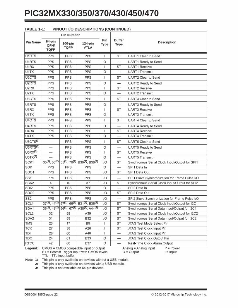
U1CTS PPS PPS PPS I ST UART1 Clear to Send
U1RTS PPS PPS PPS O — UART1 Ready to SendU1RX PPS PPS PPS I ST UART1 ReceiveU1TX PPS PPS PPS O — UART1 Transmit
U2CTS PPS PPS PPS I ST UART2 Clear to Send
U2RTS PPS PPS PPS O — UART2 Ready to SendU2RX PPS PPS PPS I ST UART2 ReceiveU2TX PPS PPS PPS O — UART2 Transmit
U3CTS PPS PPS PPS I ST UART3 Clear to Send
U3RTS PPS PPS PPS O — UART3 Ready to SendU3RX PPS PPS PPS I ST UART3 ReceiveU3TX PPS PPS PPS O — UART3 Transmit
U4CTS PPS PPS PPS I ST UART4 Clear to Send
U4RTS PPS PPS PPS O — UART4 Ready to SendU4RX PPS PPS PPS I ST UART4 ReceiveU4TX PPS PPS PPS O — UART4 Transmit
U5CTS(3) — PPS PPS I ST UART5 Clear to Send
U5RTS(3) — PPS PPS O — UART5 Ready to SendU5RX(3) — PPS PPS I ST UART5 ReceiveU5TX(3) — PPS PPS O — UART5 TransmitSCK1 35(1), 50(2) 55(1), 70(2) B30(1), B38(2) I/O ST Synchronous Serial Clock Input/Output for SPI1SDI1 PPS PPS PPS O — SPI1 Data InSDO1 PPS PPS PPS I/O ST SPI1 Data Out
SS1 PPS PPS PPS I/O — SPI1 Slave Synchronization for Frame Pulse I/OSCK2 4 10 A7 I/O ST Synchronous Serial Clock Input/Output for SPI2SDI2 PPS PPS PPS O — SPI2 Data InSDO2 PPS PPS PPS I/O ST SPI2 Data Out
SS2 PPS PPS PPS I/O — SPI2 Slave Synchronization for Frame Pulse I/OSCL1 37(1), 44(2) 57(1), 66(2) B31(1), B36(2) I/O ST Synchronous Serial Clock Input/Output for I2C1SDA1 36(1), 43(2) 56(1), 67(2) A38(1), A44(2) I/O ST Synchronous Serial Data Input/Output for I2C1SCL2 32 58 A39 I/O ST Synchronous Serial Clock Input/Output for I2C2SDA2 31 59 B32 I/O ST Synchronous Serial Data Input/Output for I2C2TMS 23 17 B9 I ST JTAG Test Mode Select PinTCK 27 38 A26 I ST JTAG Test Clock Input PinTDI 28 60 A40 I — JTAG Test Clock Input PinTDO 24 61 B33 O — JTAG Test Clock Output PinRTCC 42 68 B37 O — Real-Time Clock Alarm Output
TABLE 1-1: PINOUT I/O DESCRIPTIONS (CONTINUED)
Pin Name
Pin NumberPin
TypeBufferType Description64-pin
QFN/TQFP
100-pinTQFP
124-pinVTLA
Legend: CMOS = CMOS compatible input or output Analog = Analog input P = Power ST = Schmitt Trigger input with CMOS levels O = Output I = Input TTL = TTL input buffer
Note 1: This pin is only available on devices without a USB module.2: This pin is only available on devices with a USB module.3: This pin is not available on 64-pin devices.

2012-2017 Microchip Technology Inc. DS60001185G-page 23
PIC32MX330/350/370/430/450/470
CVREF- 15 28 A21 I Analog Comparator Voltage Reference (Low)CVREF+ 16 29 B17 I Analog Comparator Voltage Reference (High)CVREFOUT 23 34 A24 I Analog Comparator Voltage Reference (Output)C1INA 11 20 A12 I Analog
Comparator 1 Inputs C1INB 12 21 B11 I AnalogC1INC 5 11 B6 I AnalogC1IND 4 10 A7 I AnalogC2INA 13 22 A13 I Analog
Comparator 2 Inputs C2INB 14 23 B13 I AnalogC2INC 8 14 A9 I AnalogC2IND 6 12 A8 I AnalogC1OUT PPS PPS PPS O — Comparator 1 OutputC2OUT PPS PPS PPS O — Comparator 2 OutputPMALL 30 44 A29 O TTL/ST Parallel Master Port Address Latch Enable Low BytePMALH 29 43 B24 O TTL/ST Parallel Master Port Address Latch Enable High Byte
PMA0 30 44 A29 O TTL/ST Parallel Master Port Address bit 0 Input (Buffered Slave modes) and Output (Master modes)
PMA1 29 43 B24 O TTL/ST Parallel Master Port Address bit 0 Input (Buffered Slave modes) and Output (Master modes)
PMA2 8 14 A9 O TTL/ST
Parallel Master Port data (Demultiplexed Master mode) or Address/Data (Multiplexed Master modes)
PMA3 6 12 A8 O TTL/STPMA4 5 11 B6 O TTL/STPMA5 4 10 A7 O TTL/STPMA6 16 29 B17 O TTL/STPMA7 22 28 A21 O TTL/STPMA8 32 50 A32 O TTL/STPMA9 31 49 B27 O TTL/STPMA10 28 42 A28 O TTL/STPMA11 27 41 B23 O TTL/STPMA12 24 35 B20 O TTL/STPMA13 23 34 A24 O TTL/STPMA14 45 71 A46 O TTL/STPMA15 44 70 B38 O TTL/STPMCS1 45 71 A46 O TTL/STPMCS2 44 70 B38 O TTL/STPMD0 60 93 B52 I/O TTL/STPMD1 61 94 A64 I/O TTL/STPMD2 62 98 A66 I/O TTL/ST
TABLE 1-1: PINOUT I/O DESCRIPTIONS (CONTINUED)
Pin Name
Pin NumberPin
TypeBufferType Description64-pin
QFN/TQFP
100-pinTQFP
124-pinVTLA
Legend: CMOS = CMOS compatible input or output Analog = Analog input P = Power ST = Schmitt Trigger input with CMOS levels O = Output I = Input TTL = TTL input buffer
Note 1: This pin is only available on devices without a USB module.2: This pin is only available on devices with a USB module.3: This pin is not available on 64-pin devices.

PIC32MX330/350/370/430/450/470
DS60001185G-page 24 2012-2017 Microchip Technology Inc.
PMD3 63 99 B56 I/O TTL/ST
Parallel Master Port Data (Demultiplexed Master mode) or Address/Data (Multiplexed Master modes)
PMD4 64 100 A67 I/O TTL/STPMD5 1 3 B2 I/O TTL/STPMD6 2 4 A4 I/O TTL/STPMD7 3 5 B3 I/O TTL/STPMD8 — 90 A61 I/O TTL/STPMD9 — 89 B50 I/O TTL/STPMD10 — 88 A60 I/O TTL/STPMD11 — 87 B49 I/O TTL/STPMD12 — 79 B43 I/O TTL/STPMD13 — 80 A54 I/O TTL/STPMD14 — 83 B45 I/O TTL/STPMD15 — 84 A56 I/O TTL/STPMRD 53 82 A55 O — Parallel Master Port Read StrobePMWR 52 81 B44 O — Parallel Master Port Write StrobeVBUS(2) 34 54 A37 I Analog USB Bus Power Monitor
VUSB3V3(2) 35 55 B30 P — USB internal transceiver supply. If the USB module is not used, this pin must be connected to VDD.
VBUSON(2) 11 20 A12 O — USB Host and OTG bus power control OutputD+(2) 37 57 B31 I/O Analog USB D+D-(2) 36 56 A38 I/O Analog USB D-USBID(2) 33 51 A35 I ST USB OTG ID Detect
PGED1 16 25 B14 I/O ST Data I/O pin for Programming/Debugging Communication Channel 1
PGEC1 15 24 A15 I ST Clock Input pin for Programming/Debugging Communication Channel 1
PGED2 18 27 B16 I/O ST Data I/O Pin for Programming/Debugging Communication Channel 2
PGEC2 17 26 A20 I ST Clock Input Pin for Programming/Debugging Communication Channel 2
PGED3 13 22 A13 I/O ST Data I/O Pin for Programming/Debugging Communication Channel 3
PGEC3 14 23 B13 I ST Clock Input Pin for Programming/Debugging Communication Channel 3
TRCLK — 91 B51 O — Trace clockTRD0 — 97 B55 O — Trace Data bit 0TRD1 — 96 A65 O — Trace Data bit 1TRD2 — 95 B54 O — Trace Data bit 2TRD3 — 92 A62 O — Trace Data bit 3CTED1 — 17 B9 I ST CTMU External Edge Input 1CTED2 — 38 A26 I ST CTMU External Edge Input 2CTED3 18 27 B16 I ST CTMU External Edge Input 3
TABLE 1-1: PINOUT I/O DESCRIPTIONS (CONTINUED)
Pin Name
Pin NumberPin
TypeBufferType Description64-pin
QFN/TQFP
100-pinTQFP
124-pinVTLA
Legend: CMOS = CMOS compatible input or output Analog = Analog input P = Power ST = Schmitt Trigger input with CMOS levels O = Output I = Input TTL = TTL input buffer
Note 1: This pin is only available on devices without a USB module.2: This pin is only available on devices with a USB module.3: This pin is not available on 64-pin devices.

2012-2017 Microchip Technology Inc. DS60001185G-page 25
PIC32MX330/350/370/430/450/470
CTED4 22 33 B19 I ST CTMU External Edge Input 4CTED5 29 43 B24 I ST CTMU External Edge Input 5CTED6 30 44 A29 I ST CTMU External Edge Input 6CTED7 — 9 B5 I ST CTMU External Edge Input 7CTED8 — 92 A62 I ST CTMU External Edge Input 8CTED9 — 60 A40 I ST CTMU External Edge Input 9CTED10 21 32 A23 I ST CTMU External Edge Input 10CTED11 23 34 A24 I ST CTMU External Edge Input 11CTED12 15 24 A15 I ST CTMU External Edge Input 12CTED13 14 23 B13 I ST CTMU External Edge Input 13
MCLR 7 13 B7 I/P ST Master Clear (Reset) input. This pin is an active-low Reset to the device.
AVDD 19 30 A22 P P Positive supply for analog modules. This pin must be connected at all times.
AVSS 20 31 B18 P P Ground reference for analog modules
VDD10, 26, 38,
572, 16, 37, 46, 62, 86
B1, A10, A14, B21, A30, A41, A48, A59, B53
P — Positive supply for peripheral logic and I/O pins
VCAP 56 85 B48 P — Capacitor for Internal Voltage Regulator
VSS 9, 25, 41 15, 36, 45, 65, 75
A3, B8, B12, A25, B25, A43, B41,
A63
P — Ground reference for logic and I/O pins
VREF+ 16 29 B17 I Analog Analog Voltage Reference (High) InputVREF- 15 28 A21 I Analog Analog Voltage Reference (Low) Input
TABLE 1-1: PINOUT I/O DESCRIPTIONS (CONTINUED)
Pin Name
Pin NumberPin
TypeBufferType Description64-pin
QFN/TQFP
100-pinTQFP
124-pinVTLA
Legend: CMOS = CMOS compatible input or output Analog = Analog input P = Power ST = Schmitt Trigger input with CMOS levels O = Output I = Input TTL = TTL input buffer
Note 1: This pin is only available on devices without a USB module.2: This pin is only available on devices with a USB module.3: This pin is not available on 64-pin devices.

PIC32MX330/350/370/430/450/470
DS60001185G-page 26 2012-2017 Microchip Technology Inc.
NOTES:

2012-2017 Microchip Technology Inc. DS60001185G-page 27
PIC32MX330/350/370/430/450/4702.0 GUIDELINES FOR GETTING
STARTED WITH 32-BIT MCUSNote: This data sheet summarizes the features
of the PIC32MX330/350/370/430/450/470 family of devices. It is not intended to be a comprehensive reference source. To complement the information in this data sheet, refer to the documents listed in the Documentation > Reference Manual section of the Microchip PIC32 web site (www.microchip.com/pic32).
2.1 Basic Connection RequirementsGetting started with the PIC32MX330/350/370/430/450/470 family of 32-bit Microcontrollers (MCUs) requires attention to a minimal set of device pin connections before proceeding with development. The following is a list of pin names, which must always be connected:
• All VDD and VSS pins (see 2.2 “Decoupling Capacitors”)
• All AVDD and AVSS pins, even if the ADC module is not used (see 2.2 “Decoupling Capacitors”)
• VCAP pin (see 2.3 “Capacitor on Internal Voltage Regulator (VCAP)”)
• MCLR pin (see 2.4 “Master Clear (MCLR) Pin”)• PGECx/PGEDx pins, used for In-Circuit Serial
Programming (ICSP™) and debugging purposes (see 2.5 “ICSP Pins”)
• OSC1 and OSC2 pins, when external oscillator source is used (see 2.8 “External Oscillator Pins”)
The following pins may be required:
VREF+/VREF- pins, used when external voltage reference for the ADC module is implemented
Note: The AVDD and AVSS pins must be connected, regardless of ADC use and the ADC voltage reference source.
.
2.2 Decoupling CapacitorsThe use of decoupling capacitors on power supply pins, such as VDD, VSS, AVDD and AVSS is required. See Figure 2-1.
Consider the following criteria when using decoupling capacitors:
• Value and type of capacitor: A value of 0.1 μF (100 nF), 10-20V is recommended. The capacitor should be a low Equivalent Series Resistance (low-ESR) capacitor and have resonance fre-quency in the range of 20 MHz and higher. It is further recommended that ceramic capacitors be used.
• Placement on the printed circuit board: The decoupling capacitors should be placed as close to the pins as possible. It is recommended that the capacitors be placed on the same side of the board as the device. If space is constricted, the capacitor can be placed on another layer on the PCB using a via; however, ensure that the trace length from the pin to the capacitor is within one-quarter inch (6 mm) in length.
• Handling high frequency noise: If the board is experiencing high frequency noise, upward of tens of MHz, add a second ceramic-type capacitor in parallel to the above described decoupling capacitor. The value of the second capacitor can be in the range of 0.01 μF to 0.001 μF. Place this second capacitor next to the primary decoupling capacitor. In high-speed circuit designs, consider implementing a decade pair of capacitances as close to the power and ground pins as possible. For example, 0.1 μF in parallel with 0.001 μF.
• Maximizing performance: On the board layout from the power supply circuit, run the power and return traces to the decoupling capacitors first, and then to the device pins. This ensures that the decoupling capacitors are first in the power chain. Equally important is to keep the trace length between the capacitor and the power pins to a minimum thereby reducing PCB track inductance.

PIC32MX330/350/370/430/450/470
DS60001185G-page 28 2012-2017 Microchip Technology Inc.
FIGURE 2-1: RECOMMENDED MINIMUM CONNECTION
PIC32V
DD
VS
S
VDD
VSSVSS
VDD
AVD
D
AVS
S
VD
D
VS
S
0.1 μFCeramic
0.1 μFCeramic
0.1 μFCeramic
0.1 μFCeramic
C
R
VDD
MCLR
0.1 μFCeramic
L1(2)
R1
Note 1: If the USB module is not used, this pin must be connected to VDD.
2: As an option, instead of a hard-wired connection, an inductor (L1) can be substituted between VDD and AVDD to improve ADC noise rejection. The inductor impedance should be less than 3 and the inductor capacity greater than 10 mA. Where:
f FCNV
2--------------=
f 12 LC
------------------------=
L 12f C
----------------------- 2
=
(i.e., ADC conversion rate/2)
Connect(2)
VUSB3V3(1)V
CA
P
Tantalum orceramic 10 μFESR 3(3)
1: Aluminum or electrolytic capacitors should not be used. ESR 3 from -40ºC to 125ºC @ SYSCLK frequency (i.e., MIPS).
2.2.1 BULK CAPACITORSThe use of a bulk capacitor is recommended to improve power supply stability. Typical values range from 4.7 μF to 47 μF. This capacitor should be located as close to the device as possible.
2.3 Capacitor on Internal Voltage Regulator (VCAP)
2.3.1 INTERNAL REGULATOR MODEA low-ESR (3 ohm) capacitor is required on the VCAPpin, which is used to stabilize the internal voltage regu-lator output. The VCAP pin must not be connected to VDD, and must have a CEFC capacitor, with at least a 6V rating, connected to ground. The type can be ceramic or tantalum. Refer to Section 31.0 “Electrical Characteristics” for additional information on CEFCspecifications.
2.4 Master Clear (MCLR) PinThe MCLR pin provides two specific device functions: • Device Reset• Device programming and debuggingPulling The MCLR pin low generates a device Reset. Figure 2-2 illustrates a typical MCLR circuit. During device programming and debugging, the resistance and capacitance that can be added to the pin must be considered. Device programmers and debuggers drive the MCLR pin. Consequently, specific voltage levels (VIH and VIL) and fast signal transitions must not be adversely affected. Therefore, specific values of R and C will need to be adjusted based on the application and PCB requirements.For example, as illustrated in Figure 2-2, it is recommended that the capacitor C, be isolated from the MCLR pin during programming and debugging operations.Place the components illustrated in Figure 2-2 within one-quarter inch (6 mm) from the MCLR pin.
FIGURE 2-2: EXAMPLE OF MCLR PIN CONNECTIONS
Note 1: 470 R1 1k will limit any current flowing into MCLR from the external capacitor C, in the event of MCLR pin breakdown, due to Electrostatic Discharge (ESD) or Electrical Overstress (EOS). Ensure that the MCLR pin VIH and VIL specifications are met without interfering with the Debug/Programmer tools.
2: The capacitor can be sized to prevent unintentional Resets from brief glitches or to extend the device Reset period during POR.
3: No pull-ups or bypass capacitors are allowed on active debug/program PGECx/PGEDx pins.
R1(1)10k
VDD
MCLR
PIC321 k0.1 μF(2)
PGECx(3)
PGEDx(3)
ICS
P™
154236
VDDVSSNC
R
C

2012-2017 Microchip Technology Inc. DS60001185G-page 29
PIC32MX330/350/370/430/450/4702.5 ICSP PinsThe PGECx and PGEDx pins are used for In-Circuit Serial Programming™ (ICSP™) and debugging pur-poses. It is recommended to keep the trace length between the ICSP connector and the ICSP pins on the device as short as possible. If the ICSP connector is expected to experience an ESD event, a series resistor is recommended, with the value in the range of a few tens of Ohms, not to exceed 100 Ohms. Pull-up resistors, series diodes and capacitors on the PGECx and PGEDx pins are not recommended as they will interfere with the programmer/debugger communi-cations to the device. If such discrete components are an application requirement, they should be removed from the circuit during programming and debugging. Alternatively, refer to the AC/DC characteristics and timing requirements information in the respective device Flash programming specification for information on capacitive loading limits and pin input voltage high (VIH) and input low (VIL) requirements.Ensure that the “Communication Channel Select” (i.e., PGECx/PGEDx pins) programmed into the device matches the physical connections for the ICSP to MPLAB® ICD 3 or MPLAB REAL ICE™.For more information on ICD 3 and REAL ICE connection requirements, refer to the following documents that are available on the Microchip web site.• “Using MPLAB® ICD 3” (poster) DS50001765• “MPLAB® ICD 3 Design Advisory” DS50001764• “MPLAB® REAL ICE™ In-Circuit Debugger
User’s Guide” DS50001616• “Using MPLAB® REAL ICE™ Emulator” (poster)
DS50001749
2.6 JTAGThe TMS, TDO, TDI and TCK pins are used for testing and debugging according to the Joint Test Action Group (JTAG) standard. It is recommended to keep the trace length between the JTAG connector and the JTAG pins on the device as short as possible. If the JTAG connector is expected to experience an ESD event, a series resistor is recommended, with the value in the range of a few tens of Ohms, not to exceed 100 Ohms.
Pull-up resistors, series diodes and capacitors on the TMS, TDO, TDI and TCK pins are not recommended as they will interfere with the programmer/debugger communications to the device. If such discrete compo-nents are an application requirement, they should be removed from the circuit during programming and debugging. Alternatively, refer to the AC/DC character-istics and timing requirements information in the respective device Flash programming specification for information on capacitive loading limits and pin input voltage high (VIH) and input low (VIL) requirements.
2.7 TraceThe trace pins can be connected to a hardware trace-enabled programmer to provide a compressed real-time instruction trace. When used for trace, the TRD3, TRD2, TRD1, TRD0 and TRCLK pins should be dedicated for this use. The trace hardware requires a 22 Ohm series resistor between the trace pins and the trace connector.
2.8 External Oscillator PinsMany MCUs have options for at least two oscillators: a high-frequency primary oscillator and a low-frequency secondary oscillator (refer to Section 8.0 “OscillatorConfiguration” for details).
The oscillator circuit should be placed on the same side of the board as the device. Also, place the oscillator cir-cuit close to the respective oscillator pins, not exceed-ing one-half inch (12 mm) distance between them. The load capacitors should be placed next to the oscillator itself, on the same side of the board. Use a grounded copper pour around the oscillator circuit to isolate them from surrounding circuits. The grounded copper pour should be routed directly to the MCU ground. Do not run any signal traces or power traces inside the ground pour. Also, if using a two-sided board, avoid any traces on the other side of the board where the crystal is placed. A suggested layout is illustrated in Figure 2-3.
FIGURE 2-3: SUGGESTED OSCILLATOR CIRCUIT PLACEMENT
Main Oscillator
Guard Ring
Guard Trace
SecondaryOscillator

PIC32MX330/350/370/430/450/470
DS60001185G-page 30 2012-2017 Microchip Technology Inc.
2.8.1 CRYSTAL OSCILLATOR DESIGN CONSIDERATION
The following example assumptions are used to calculate the Primary Oscillator loading capacitor values:
• CIN = PIC32_OSC2_Pin Capacitance = ~4-5 pF• COUT = PIC32_OSC1_Pin Capacitance = ~4-5 pF• C1 and C2 = XTAL manufacturing recommended
loading capacitance• Estimated PCB stray capacitance, (i.e.,12 mm
length) = 2.5 pF
EXAMPLE 2-1: CRYSTAL LOAD CAPACITOR CALCULATION
The following tips are used to increase oscillator gain, (i.e., to increase peak-to-peak oscillator signal):
• Select a crystal with a lower “minimum” power drive rating
• Select an crystal oscillator with a lower XTAL manufacturing “ESR” rating.
• Add a parallel resistor across the crystal. The smaller the resistor value the greater the gain. It is recom-mended to stay in the range of 600k to 1M
• C1 and C2 values also affect the gain of the oscillator. The lower the values, the higher the gain.
• C2/C1 ratio also affects gain. To increase the gain, make C1 slightly smaller than C2, which will also help start-up performance.
Note: Do not add excessive gain such that the oscillator signal is clipped, flat on top of the sine wave. If so, you need to reduce the gain or add a series resistor, RS, as shown in circuit “C” in Figure 2-4. Failure to do so will stress and age the crystal, which can result in an early failure. Adjust the gain to trim the max peak-to-peak to ~VDD-0.6V. When measuring the oscilla-tor signal you must use a FET scope probe or a probe with 1.5 pF or the scope probe itself will unduly change the gain and peak-to-peak levels.
2.8.1.1 Additional Microchip References• AN588 “PICmicro® Microcontroller Oscillator
Design Guide”• AN826 “Crystal Oscillator Basics and Crystal
Selection for rfPIC™ and PICmicro® Devices”• AN849 “Basic PICmicro® Oscillator Design”
FIGURE 2-4: PRIMARY CRYSTAL OSCILLATOR CIRCUIT RECOMMENDATIONS
OSC2 OSC1
1M
Typical XT(4-10 MHz)
Circuit A
C1
C2
OSC2 OSC1
Typical HS(10-25 MHz)
Circuit B
C1
C2
Rs
OSC2 OSC1
1M
Typical XT/HS(4-25 MHz)
Circuit C
C1
C2
1MRs
OSC2 OSC1
Not RecommendedCircuit D
Not Recommended
1M
Rs
OSC2 OSC1
Circuit E
Crystal manufacturer recommended: C1 = C2 = 15 pF
Therefore:CLOAD = {( [CIN + C1] * [COUT + C2] ) / [CIN + C1 + C2 + COUT] } + estimated oscillator PCB stray capacitance
= {( [5 + 15][5 + 15] ) / [5 + 15 + 15 + 5] } + 2.5 pF
= {( [20][20]) / [40] } + 2.5 = 10 + 2.5 = 12.5 pF
Rounded to the nearest standard value or 13 pF in this example for Primary Oscillator crystals “C1” and “C2”.

2012-2017 Microchip Technology Inc. DS60001185G-page 31
PIC32MX330/350/370/430/450/4702.9 Unused I/OsUnused I/O pins should not be allowed to float as inputs. They can be configured as outputs and driven to a logic-low state.
Alternatively, inputs can be reserved by connecting the pin to VSS through a 1k to 10k resistor and configuring the pin as an input.
2.10 EMI/EMC/EFT (IEC 61000-4-4 and IEC 61000-4-2) Suppression Considerations
The use of LDO regulators is preferred to reduce overall system noise and provide a cleaner power source. However, when utilizing switching Buck/Boost regulators as the local power source for PIC32 devices, as well as in electrically noisy environ-ments or test conditions required for IEC 61000-4-4 and IEC 61000-4-2, users should evaluate the use of T-Filters (i.e., L-C-L) on the power pins, as shown in Figure 2-5. In addition to a more stable power source, use of this type of T-Filter can greatly reduce susceptibility to EMI sources and events.
FIGURE 2-5: EMI/EMC/EFT SUPPRESSION CIRCUIT
VSS
VDDVSS
VUSB3V3
VSS
VDD
VSSVDD
VD
DV
SS
VS
SV
DD
VSSVDD
VS
SV
DD
AV
DD
AV
SS
FerriteChips
0.01 μF
0.01 μFVDD
VDD
0.1 μF
0.1 μF
0.1 μF0.1 μF
0.1 μF0.1 μF
0.1 μF
0.1 μF
FerriteChips
Ferrite Chip SMDDCR = 0.15 (max)600 ma ISAT300 @ 100 MHzPN#: 1-1624117-3
0.1 μF
PIC32

PIC32MX330/350/370/430/450/470
DS60001185G-page 32 2012-2017 Microchip Technology Inc.
2.11 Typical Application Connection Examples
Examples of typical application connections are shown in Figure 2-6, Figure 2-7, and Figure 2-8.
FIGURE 2-6: CAPACITIVE TOUCH SENSING WITH GRAPHICS APPLICATION
CTMU
Current Source
ADC
MicrochipmTouch™
Library
UserApplication
MicrochipGraphicsLibrary
Read the Touch Sensors
Process Samples
Display Data
ParallelMaster
Port
LCD Controller
FrameBuffer
DisplayController
PMD<7:0>LCDPanel
PIC32MX430F064L
To AN6 To AN7 To AN8 To AN11
C1
R3
C2
R2
R3
R1
C5
C5
C5C1
R1 R1 R1
C3
R2
C3
R2
C1
R2
C2
R3
C2
R3
C3
AN0
AN1
AN11
To AN0
To AN1
To AN5
AN9
PMWR
To AN9
R1
C4
R2
C4
R3
C4
FIGURE 2-7: AUDIO PLAYBACK APPLICATION
AudioCodec
DisplayPMP
I2S
SPI
USBUSBPMD<7:0>
3
3
Stereo Headphones
Speaker
PIC32MX450F256L
Host
PMWR
MMC SD3
SDI
REFCLKO

2012-2017 Microchip Technology Inc. DS60001185G-page 33
PIC32MX330/350/370/430/450/470FIGURE 2-8: LOW-COST CONTROLLERLESS (LCC) GRAPHICS APPLICATION WITH
PROJECTED CAPACITIVE TOUCH
LCD Display
PIC32MX430F064L
SRAM
CTMU
Microchip mTouch™
DMA PMP
ADC
Projected CapacitiveTouch Overlay
GFX Libraries
External Frame Buffer
ANx

PIC32MX330/350/370/430/450/470
DS60001185G-page 34 2012-2017 Microchip Technology Inc.
NOTES:

2012-2017 Microchip Technology Inc. DS60001185G-page 35
PIC32MX330/350/370/430/450/4703.0 CPU
Note: This data sheet summarizes the features of the PIC32MX330/350/370/430/450/470 family of devices. It is not intended to be a comprehensive reference source. To complement the information in this data sheet, refer to Section 2. “CPU”(DS60001113), which is available from the Documentation > Reference Manual section of the Microchip PIC32 web site (www.microchip.com/pic32). Resources for the MIPS32® M4K® Processor Core are available at http://www.imgtec.com.
The the MIPS32® M4K® Processor Core is the heart of the PIC32MX330/350/370/430/450/470 device proces-sor. The CPU fetches instructions, decodes each instruction, fetches source operands, executes each instruction and writes the results of instruction execution to the proper destinations.
3.1 Features• 5-stage pipeline• 32-bit address and data paths• MIPS32® Enhanced Architecture (Release 2):
- Multiply-accumulate and multiply-subtract instructions
- Targeted multiply instruction- Zero/One detect instructions- WAIT instruction- Conditional move instructions (MOVN, MOVZ)- Vectored interrupts- Programmable exception vector base- Atomic interrupt enable/disable- GPR shadow registers to minimize latency
for interrupt handlers- Bit field manipulation instructions
• MIPS16e® Code Compression:- 16-bit encoding of 32-bit instructions to
improve code density- Special PC-relative instructions for efficient
loading of addresses and constants- SAVE and RESTORE macro instructions for
setting up and tearing down stack frames within subroutines
- Improved support for handling 8 and 16-bit data types
• Simple Fixed Mapping Translation (FMT) Mechanism:
• Simple Dual Bus Interface:- Independent 32-bit address and data buses- Transactions can be aborted to improve
interrupt latency• Autonomous Multiply/Divide Unit (MDU):
- Maximum issue rate of one 32x16 multiply per clock
- Maximum issue rate of one 32x32 multiply every other clock
- Early-in iterative divide. Minimum 11 and maximum 33 clock latency (dividend (rs) sign extension-dependent)
• Power Control:- Minimum frequency: 0 MHz- Low-Power mode (triggered by WAIT instruction)- Extensive use of local gated clocks
• EJTAG Debug and Instruction Trace:- Support for single stepping- Virtual instruction and data address/value- Breakpoints
FIGURE 3-1: MIPS32® M4K® PROCESSOR CORE BLOCK DIAGRAM
CPUMDU
Execution Core(RF/ALU/Shift) FMT
TAP
EJTAG
Bus Interface
PowerManagement
SystemCo-processor
Off-chip Debug Interface
Bus MatrixDual Bus Interface

PIC32MX330/350/370/430/450/470
DS60001185G-page 36 2012-2017 Microchip Technology Inc.
3.2 Architecture OverviewThe MIPS32® M4K® processor core contains several logic blocks working together in parallel, providing an efficient high-performance computing engine. The following blocks are included with the core:
• Execution Unit• Multiply/Divide Unit (MDU)• System Control Coprocessor (CP0)• Fixed Mapping Translation (FMT)• Dual Internal Bus interfaces• Power Management• MIPS16e® Support• Enhanced JTAG (EJTAG) Controller
3.2.1 EXECUTION UNITThe MIPS32® M4K® processor core execution unit implements a load/store architecture with single-cycle ALU operations (logical, shift, add, subtract) and an autonomous multiply/divide unit. The core contains thirty-two 32-bit General Purpose Registers (GPRs) used for integer operations and address calculation. One additional register file shadow set (containing thirty-two registers) is added to minimize context switching overhead during interrupt/exception process-ing. The register file consists of two read ports and one write port and is fully bypassed to minimize operation latency in the pipeline.
The execution unit includes:
• 32-bit adder used for calculating the data address• Address unit for calculating the next instruction
address• Logic for branch determination and branch target
address calculation• Load aligner• Bypass multiplexers used to avoid stalls when
executing instruction streams where data producing instructions are followed closely by consumers of their results
• Leading Zero/One detect unit for implementing the CLZ and CLO instructions
• Arithmetic Logic Unit (ALU) for performing bitwise logical operations
• Shifter and store aligner
3.2.2 MULTIPLY/DIVIDE UNIT (MDU)The MIPS32® M4K® processor core includes a Multi-ply/Divide Unit (MDU) that contains a separate pipeline for multiply and divide operations. This pipeline oper-ates in parallel with the Integer Unit (IU) pipeline and does not stall when the IU pipeline stalls. This allows MDU operations to be partially masked by system stalls and/or other integer unit instructions.
The high-performance MDU consists of a 32x16 booth recoded multiplier, result/accumulation registers (HI and LO), a divide state machine, and the necessary multiplexers and control logic. The first number shown (‘32’ of 32x16) represents the rs operand. The second number (‘16’ of 32x16) represents the rt operand. The PIC32 core only checks the value of the latter (rt) oper-and to determine how many times the operation must pass through the multiplier. The 16x16 and 32x16 operations pass through the multiplier once. A 32x32 operation passes through the multiplier twice.
The MDU supports execution of one 16x16 or 32x16 multiply operation every clock cycle; 32x32 multiply operations can be issued every other clock cycle. Appropriate interlocks are implemented to stall the issuance of back-to-back 32x32 multiply operations. The multiply operand size is automatically determined by logic built into the MDU.
Divide operations are implemented with a simple 1 bit per clock iterative algorithm. An early-in detection checks the sign extension of the dividend (rs) operand. If rs is 8 bits wide, 23 iterations are skipped. For a 16-bit wide rs, 15 iterations are skipped and for a 24-bit wide rs, 7 iterations are skipped. Any attempt to issue a sub-sequent MDU instruction while a divide is still active causes an IU pipeline stall until the divide operation is completed.
Table 3-1 lists the repeat rate (peak issue rate of cycles until the operation can be reissued) and latency (num-ber of cycles until a result is available) for the PIC32 core multiply and divide instructions. The approximate latency and repeat rates are listed in terms of pipeline clocks.
TABLE 3-1: MIPS32® M4K® PROCESSOR CORE HIGH-PERFORMANCE INTEGER MULTIPLY/DIVIDE UNIT LATENCIES AND REPEAT RATES
Op code Operand Size (mul rt) (div rs) Latency Repeat Rate
MULT/MULTU, MADD/MADDU, MSUB/MSUBU
16 bits 1 132 bits 2 2
MUL 16 bits 2 132 bits 3 2
DIV/DIVU 8 bits 12 1116 bits 19 1824 bits 26 2532 bits 33 32

2012-2017 Microchip Technology Inc. DS60001185G-page 37
PIC32MX330/350/370/430/450/470The MIPS architecture defines that the result of a multiply or divide operation be placed in the HI and LO registers. Using the Move-From-HI (MFHI) and Move-From-LO (MFLO) instructions, these values can be transferred to the General Purpose Register file.
In addition to the HI/LO targeted operations, the MIPS32® architecture also defines a multiply instruction, MUL, which places the least significant results in the pri-mary register file instead of the HI/LO register pair. By avoiding the explicit MFLO instruction required when using the LO register, and by supporting multiple desti-nation registers, the throughput of multiply-intensive operations is increased.
Two other instructions, Multiply-Add (MADD) and Multiply-Subtract (MSUB), are used to perform the multiply-accumulate and multiply-subtract operations. The MADD instruction multiplies two numbers and then adds the product to the current contents of the HI and LO registers. Similarly, the MSUB instruction multiplies two operands and then subtracts the product from the HI and LO registers. The MADD and MSUB operations are commonly used in DSP algorithms.
3.2.3 SYSTEM CONTROL COPROCESSOR (CP0)
In the MIPS architecture, CP0 is responsible for the virtual-to-physical address translation, the exception control system, the processor’s diagnostics capability, the operating modes (Kernel, User and Debug) and whether interrupts are enabled or disabled. Configura-tion information, such as presence of options like MIPS16e®, is also available by accessing the CP0 registers, listed in Table 3-2.
TABLE 3-2: COPROCESSOR 0 REGISTERSRegisterNumber
Register Name Function
0-6 Reserved Reserved in the PIC32MX330/350/370/430/450/470 family core.7 HWREna Enables access via the RDHWR instruction to selected hardware registers.8 BadVAddr(1) Reports the address for the most recent address-related exception.9 Count(1) Processor cycle count.10 Reserved Reserved in the PIC32MX330/350/370/430/450/470 family core.11 Compare(1) Timer interrupt control.12 Status(1) Processor status and control.12 IntCtl(1) Interrupt system status and control.12 SRSCtl(1) Shadow register set status and control.12 SRSMap(1) Provides mapping from vectored interrupt to a shadow set.13 Cause(1) Cause of last general exception.14 EPC(1) Program counter at last exception.15 PRId Processor identification and revision.15 EBASE Exception vector base register.16 Config Configuration register.16 Config1 Configuration register 1.16 Config2 Configuration register 2.16 Config3 Configuration register 3.
17-22 Reserved Reserved in the PIC32MX330/350/370/430/450/470 family core.23 Debug(2) Debug control and exception status.24 DEPC(2) Program counter at last debug exception.
25-29 Reserved Reserved in the PIC32MX330/350/370/430/450/470 family core.30 ErrorEPC(1) Program counter at last error.31 DESAVE(2) Debug handler scratchpad register.
Note 1: Registers used in exception processing.2: Registers used during debug.

PIC32MX330/350/370/430/450/470
DS60001185G-page 38 2012-2017 Microchip Technology Inc.
Coprocessor 0 also contains the logic for identifying and managing exceptions. Exceptions can be caused by a variety of sources, including alignment errors in data, external events or program errors. Table 3-3 lists the exception types in order of priority.
TABLE 3-3: MIPS32® M4K® PROCESSOR CORE EXCEPTION TYPESException Description
Reset Assertion MCLR or a Power-on Reset (POR).DSS EJTAG debug single step.DINT EJTAG debug interrupt. Caused by the assertion of the external EJ_DINT input or by setting the
EjtagBrk bit in the ECR register.NMI Assertion of NMI signal.Interrupt Assertion of unmasked hardware or software interrupt signal.DIB EJTAG debug hardware instruction break matched.AdEL Fetch address alignment error. Fetch reference to protected address.IBE Instruction fetch bus error.DBp EJTAG breakpoint (execution of SDBBP instruction).Sys Execution of SYSCALL instruction.Bp Execution of BREAK instruction.RI Execution of a reserved instruction.CpU Execution of a coprocessor instruction for a coprocessor that is not enabled.CEU Execution of a CorExtend instruction when CorExtend is not enabled.Ov Execution of an arithmetic instruction that overflowed.Tr Execution of a trap (when trap condition is true).DDBL/DDBS EJTAG Data Address Break (address only) or EJTAG data value break on store (address + value).AdEL Load address alignment error. Load reference to protected address.AdES Store address alignment error. Store to protected address.DBE Load or store bus error.DDBL EJTAG data hardware breakpoint matched in load data compare.
3.3 Power ManagementThe MIPS® M4K® processor core offers a number of power management features, including low-power design, active power management and power-down modes of operation. The core is a static design that supports slowing or Halting the clocks, which reduces system power consumption during Idle periods.
3.3.1 INSTRUCTION-CONTROLLED POWER MANAGEMENT
The mechanism for invoking Power-Down mode is through execution of the WAIT instruction. For more information on power management, see Section 27.0 “Power-Saving Features”.
3.3.2 LOCAL CLOCK GATINGThe majority of the power consumed by the PIC32MX330/350/370/430/450/470 family core is in the clock tree and clocking registers. The PIC32MX family uses extensive use of local gated-clocks to reduce this dynamic power consumption.
3.4 EJTAG Debug SupportThe MIPS® M4K® processor core provides for an Enhanced JTAG (EJTAG) interface for use in the soft-ware debug of application and kernel code. In addition to standard User mode and Kernel modes of operation, the M4K® core provides a Debug mode that is entered after a debug exception (derived from a hardware breakpoint, single-step exception, etc.) is taken and continues until a Debug Exception Return (DERET) instruction is executed. During this time, the processor executes the debug exception handler routine.
The EJTAG interface operates through the Test Access Port (TAP), a serial communication port used for trans-ferring test data in and out of the core. In addition to the standard JTAG instructions, special instructions defined in the EJTAG specification define which registers are selected and how they are used.

2012-2017 Microchip Technology Inc. DS60001185G-page 39
PIC32MX330/350/370/430/450/4704.0 MEMORY ORGANIZATION
Note: This data sheet summarizes the features of the PIC32MX330/350/370/430/450/470 family of devices. It is not intended to be a comprehensive reference source.For detailed information, refer to Section 3. “Memory Organization”(DS60001115), which is available from the Documentation > Reference Manual section of the Microchip PIC32 web site (www.microchip.com/pic32).
PIC32MX330/350/370/430/450/470 microcontrollers provide 4 GB of unified virtual memory address space. All memory regions, including program, data memory, SFRs and Configuration registers, reside in this address space at their respective unique addresses. The program and data memories can be optionally par-titioned into user and kernel memories. In addition, the data memory can be made executable, allowing PIC32MX330/350/370/430/450/470 devices to execute from data memory.
Key features include:• 32-bit native data width• Separate User (KUSEG) and Kernel (KSEG0/
KSEG1) mode address space• Flexible program Flash memory partitioning• Flexible data RAM partitioning for data and
program space• Separate boot Flash memory for protected code• Robust bus exception handling to intercept
runaway code• Simple memory mapping with Fixed Mapping
Translation (FMT) unit• Cacheable (KSEG0) and non-cacheable (KSEG1)
address regions
4.1 Memory LayoutPIC32MX330/350/370/430/450/470 microcontrollers implement two address schemes: virtual and physical. All hardware resources, such as program memory, data memory and peripherals, are located at their respective physical addresses. Virtual addresses are exclusively used by the CPU to fetch and execute instructions as well as access peripherals. Physical addresses are used by bus master peripherals, such as DMA and the Flash controller, that access memory independently of the CPU.
The memory maps for the PIC32MX330/350/370/430/450/470 devices are illustrated in Figure 4-1 throughFigure 4-4.

PIC32MX330/350/370/430/450/470
DS60001185G-page 40 2012-2017 Microchip Technology Inc.
FIGURE 4-1: MEMORY MAP FOR DEVICES WITH 64 KB OF PROGRAM MEMORYVirtual
Memory Map(1) Physical Memory Map(1)
0xFFFFFFFFReserved
Reserved
0xFFFFFFFF0xBFC030000xBFC02FFF Device
Configuration Registers0xBFC02FF0
0xBFC02FEFBoot Flash
0xBFC00000
Reserved0xBF9000000xBF8FFFFF
SFRs0xBF800000
Reserved0xBD0100000xBD00FFFF
Program Flash(2)
0xBD000000
Reserved0xA00040000xA0003FFF
RAM(2)
0xA0000000 0x1FC03000
Reserved DeviceConfiguration
Registers
0x1FC02FFF0x9FC030000x9FC02FFF Device
ConfigurationRegisters
0x1FC02FF0
Boot Flash0x1FC02FEF
0x9FC02FF00x9FC02FEF
Boot Flash0x1FC00000
Reserved0x9FC00000 0x1F900000
Reserved SFRs0x1F8FFFFF
0x9D010000 0x1F8000000x9D00FFFF
Program Flash(2) Reserved0x9D000000 0x1D010000
ReservedProgram Flash(2)
0x1D00FFFF0x800040000x80003FFF
RAM(2)0x1D000000
Reserved0x80000000 0x00004000
Reserved RAM(2) 0x00003FFF0x00000000 0x00000000
Note 1: Memory areas are not shown to scale.2: The size of this memory region is programmable (see Section 3. “Memory Organization”
(DS60001115) in the “PIC32 Family Reference Manual”) and can be changed by initializa-tion code provided by end-user development tools (refer to the specific development tool documentation for information).
KSE
G1
KSE
G0

2012-2017 Microchip Technology Inc. DS60001185G-page 41
PIC32MX330/350/370/430/450/470FIGURE 4-2: MEMORY MAP FOR DEVICES WITH 128 KB OF PROGRAM MEMORY
VirtualMemory Map(1) Physical
Memory Map(1)
0xFFFFFFFFReserved
Reserved
0xFFFFFFFF0xBFC030000xBFC02FFF Device
Configuration Registers0xBFC02FF0
0xBFC02FEFBoot Flash
0xBFC00000
Reserved0xBF9000000xBF8FFFFF
SFRs0xBF800000
Reserved0xBD0200000xBD01FFFF
Program Flash(2)
0xBD000000
Reserved0xA00080000xA0007FFF
RAM(2)
0xA0000000 0x1FC03000
Reserved DeviceConfiguration
Registers
0x1FC02FFF0x9FC030000x9FC02FFF Device
ConfigurationRegisters
0x1FC02FF0
Boot Flash0x1FC02FEF
0x9FC02FF00x9FC02FEF
Boot Flash0x1FC00000
Reserved0x9FC00000 0x1F900000
Reserved SFRs0x1F8FFFFF
0x9D020000 0x1F8000000x9D01FFFF
Program Flash(2) Reserved0x9D000000 0x1D020000
ReservedProgram Flash(2)
0x1D01FFFF0x800080000x80007FFF
RAM(2)0x1D000000
Reserved0x80000000 0x00008000
Reserved RAM(2) 0x00007FFF0x00000000 0x00000000
Note 1: Memory areas are not shown to scale.2: The size of this memory region is programmable (see Section 3. “Memory Organization”
(DS60001115) in the “PIC32 Family Reference Manual”) and can be changed by initializa-tion code provided by end-user development tools (refer to the specific development tool documentation for information).
KSE
G1
KSE
G0

PIC32MX330/350/370/430/450/470
DS60001185G-page 42 2012-2017 Microchip Technology Inc.
FIGURE 4-3: MEMORY MAP FOR DEVICES WITH 256 KB OF PROGRAM MEMORYVirtual
Memory Map(1) Physical Memory Map(1)
0xFFFFFFFFReserved
Reserved
0xFFFFFFFF0xBFC030000xBFC02FFF Device
Configuration Registers0xBFC02FF0
0xBFC02FEFBoot Flash
0xBFC00000
Reserved0xBF9000000xBF8FFFFF
SFRs0xBF800000
Reserved0xBD0400000xBD03FFFF
Program Flash(2)
0xBD000000
Reserved0xA00100000xA000FFFF
RAM(2)
0xA0000000 0x1FC03000
Reserved DeviceConfiguration
Registers
0x1FC02FFF0x9FC030000x9FC02FFF Device
ConfigurationRegisters
0x1FC02FF0
Boot Flash0x1FC02FEF
0x9FC02FF00x9FC02FEF
Boot Flash0x1FC00000
Reserved0x9FC00000 0x1F900000
Reserved SFRs0x1F8FFFFF
0x9D040000 0x1F8000000x9D03FFFF
Program Flash(2) Reserved0x9D000000 0x1D040000
ReservedProgram Flash(2)
0x1D03FFFF0x800100000x8000FFFF
RAM(2)0x1D000000
Reserved0x80000000 0x00010000
Reserved RAM(2) 0x0000FFFF0x00000000 0x00000000
Note 1: Memory areas are not shown to scale.2: The size of this memory region is programmable (see Section 3. “Memory Organization”
(DS60001115) in the “PIC32 Family Reference Manual”) and can be changed by initializa-tion code provided by end-user development tools (refer to the specific development tool documentation for information).
KSE
G1
KSE
G0

2012-2017 Microchip Technology Inc. DS60001185G-page 43
PIC32MX330/350/370/430/450/470FIGURE 4-4: MEMORY MAP FOR DEVICES WITH 512 KB OF PROGRAM MEMORY
VirtualMemory Map(1) Physical
Memory Map(1)
0xFFFFFFFFReserved
Reserved
0xFFFFFFFF0xBFC030000xBFC02FFF Device
Configuration Registers0xBFC02FF0
0xBFC02FEFBoot Flash
0xBFC00000
Reserved0xBF9000000xBF8FFFFF
SFRs0xBF800000
Reserved0xBD0800000xBD07FFFF
Program Flash(2)
0xBD000000
Reserved0xA00200000xA001FFFF
RAM(2)
0xA0000000 0x1FC03000
Reserved DeviceConfiguration
Registers
0x1FC02FFF0x9FC030000x9FC02FFF Device
ConfigurationRegisters
0x1FC02FF0
Boot Flash0x1FC02FEF
0x9FC02FF00x9FC02FEF
Boot Flash0x1FC00000
Reserved0x9FC00000 0x1F900000
Reserved SFRs0x1F8FFFFF
0x9D080000 0x1F8000000x9D07FFFF
Program Flash(2) Reserved0x9D000000 0x1D080000
ReservedProgram Flash(2)
0x1D07FFFF0x800200000x8001FFFF
RAM(2)0x1D000000
Reserved0x80000000 0x00020000
Reserved RAM(2) 0x0001FFFF0x00000000 0x00000000
Note 1: Memory areas are not shown to scale.2: The size of this memory region is programmable (see Section 3. “Memory Organization”
(DS60001115) in the “PIC32 Family Reference Manual”) and can be changed by initializa-tion code provided by end-user development tools (refer to the specific development tool documentation for information).
KSE
G1
KSE
G0

PIC32MX330/350/370/430/450/470
DS60001185G-page 44 2012-2017 Microchip Technology Inc.
TABLE 4-1: SFR MEMORY MAP
PeripheralVirtual Address
Base Offset Start
Watchdog Timer
0xBF80
0x0000
RTCC 0x0200
Timer1-5 0x0600
Input Capture 1-5 0x2000
Output Compare 1-5 0x3000
I2C1 and I2C2 0x5000
SPI1 and SPI2 0x5800
UART1 and UART2 0x6000
PMP 0x7000
ADC 0x9000
CVREF 0x9800
Comparator 0xA000
CTMU 0xA200
Oscillator 0xF000
Device and Revision ID 0xF200
Flash Controller 0xF400
Reset 0xF600
PPS 0xFA04
Interrupts
0xBF88
0x1000
Bus Matrix 0x2000
DMA 0x3000
Prefetch 0x4000
USB 0x5040
PORTA-PORTG 0x6000
Configuration 0xBFC0 0x2FF0

2012-2017 M
icrochip Technology Inc.D
S60001185G
-page
45
PIC32M
X330/350/370/430/450/470
4.2 Bus Matrix Registers TABLE 4-2: BUS MATRIX REGISTER MAP
Virtu
al A
ddre
ss(B
F88_
#)
Reg
iste
rN
ame
Bit
Ran
ge
Bits
All
Res
ets
31/15 30/14 29/13 28/12 27/11 26/10 25/9 24/8 23/7 22/6 21/5 20/4 19/3 18/2 17/1 16/0
2000 BMXCON(1)31:16 — — — — — BMXCHEDMA — — — — — BMXERRIXI BMXERRICD BMXERRDMA BMXERRDS BMXERRIS 041F
15:0 — — — — — — — — — BMXWSDRM — — — BMXARB<2:0> 0047
2010 BMXDKPBA(1) 31:16 — — — — — — — — — — — — — — — — 0000
15:0 BMXDKPBA<15:0> 0000
2020 BMXDUDBA(1) 31:16 — — — — — — — — — — — — — — — — 0000
15:0 BMXDUDBA<15:0> 0000
2030 BMXDUPBA(1) 31:16 — — — — — — — — — — — — — — — — 0000
15:0 BMXDUPBA<15:0> 0000
2040 BMXDRMSZ31:16
BMXDRMSZ<31:0>xxxx
15:0 xxxx
2050 BMXPUPBA(1) 31:16 — — — — — — — — — — — — BMXPUPBA<19:16> 0000
15:0 BMXPUPBA<15:0> 0000
2060 BMXPFMSZ31:16
BMXPFMSZ<31:0>xxxx
15:0 xxxx
2070 BMXBOOTSZ31:16
BMXBOOTSZ<31:0>0000
15:0 0000
Legend: x = unknown value on Reset; — = unimplemented, read as ‘0’. Reset values are shown in hexadecimal.
Note 1: This register has corresponding CLR, SET and INV registers at its virtual address, plus an offset of 0x4, 0x8 and 0xC, respectively. See Section 12.2 “CLR, SET, and INV Registers” for more information.

PIC32MX330/350/370/430/450/470
DS60001185G-page 46 2012-2017 Microchip Technology Inc.
REGISTER 4-1: BMXCON: BUS MATRIX CONFIGURATION REGISTER Bit
RangeBit
31/23/15/7Bit
30/22/14/6Bit
29/21/13/5Bit
28/20/12/4Bit
27/19/11/3Bit
26/18/10/2Bit
25/17/9/1Bit
24/16/8/0
31:24U-0 U-0 U-0 U-0 U-0 R/W-1 U-0 U-0
— — — — — BMXCHEDMA — —
23:16U-0 U-0 U-0 R/W-1 R/W-1 R/W-1 R/W-1 R/W-1
— — — BMXERRIXI
BMXERRICD
BMXERRDMA
BMXERRDS
BMXERRIS
15:8U-0 U-0 U-0 U-0 U-0 U-0 U-0 U-0— — — — — — — —
7:0U-0 R/W-1 U-0 U-0 U-0 R/W-0 R/W-0 R/W-1
— BMXWSDRM — — — BMXARB<2:0>
Legend:R = Readable bit W = Writable bit U = Unimplemented bit, read as ‘0’-n = Value at POR ‘1’ = Bit is set ‘0’ = Bit is cleared
bit 31-27 Unimplemented: Read as ‘0’bit 26 BMXCHEDMA: BMX PFM Cacheability for DMA Accesses bit
1 = Enable program Flash memory (data) cacheability for DMA accesses (requires cache to have data cach-ing enabled)
0 = Disable program Flash memory (data) cacheability for DMA accesses (hits are still read from the cache, but misses do not update the cache)
bit 25-21 Unimplemented: Read as ‘0’bit 20 BMXERRIXI: Enable Bus Error from IXI bit
1 = Enable bus error exceptions for unmapped address accesses initiated from IXI shared bus0 = Disable bus error exceptions for unmapped address accesses initiated from IXI shared bus
bit 19 BMXERRICD: Enable Bus Error from ICD Debug Unit bit1 = Enable bus error exceptions for unmapped address accesses initiated from ICD0 = Disable bus error exceptions for unmapped address accesses initiated from ICD
bit 18 BMXERRDMA: Bus Error from DMA bit1 = Enable bus error exceptions for unmapped address accesses initiated from DMA0 = Disable bus error exceptions for unmapped address accesses initiated from DMA
bit 17 BMXERRDS: Bus Error from CPU Data Access bit (disabled in Debug mode)1 = Enable bus error exceptions for unmapped address accesses initiated from CPU data access0 = Disable bus error exceptions for unmapped address accesses initiated from CPU data access
bit 16 BMXERRIS: Bus Error from CPU Instruction Access bit (disabled in Debug mode)1 = Enable bus error exceptions for unmapped address accesses initiated from CPU instruction access0 = Disable bus error exceptions for unmapped address accesses initiated from CPU instruction access
bit 15-7 Unimplemented: Read as ‘0’bit 6 BMXWSDRM: CPU Instruction or Data Access from Data RAM Wait State bit
1 = Data RAM accesses from CPU have one wait state for address setup0 = Data RAM accesses from CPU have zero wait states for address setup
bit 5-3 Unimplemented: Read as ‘0’bit 2-0 BMXARB<2:0>: Bus Matrix Arbitration Mode bits
111 = Reserved (using these configuration modes will produce undefined behavior)•••011 = Reserved (using these configuration modes will produce undefined behavior)010 = Arbitration Mode 2001 = Arbitration Mode 1 (default)000 = Arbitration Mode 0

2012-2017 Microchip Technology Inc. DS60001185G-page 47
PIC32MX330/350/370/430/450/470
REGISTER 4-2: BMXDKPBA: DATA RAM KERNEL PROGRAM BASE ADDRESS REGISTER Bit
RangeBit
31/23/15/7Bit
30/22/14/6Bit
29/21/13/5Bit
28/20/12/4Bit
27/19/11/3Bit
26/18/10/2Bit
25/17/9/1Bit
24/16/8/0
31:24U-0 U-0 U-0 U-0 U-0 U-0 U-0 U-0
— — — — — — — —
23:16U-0 U-0 U-0 U-0 U-0 U-0 U-0 U-0
— — — — — — — —
15:8R/W-0 R/W-0 R/W-0 R/W-0 R/W-0 R/W-0 R-0 R-0
BMXDKPBA<15:8>
7:0R-0 R-0 R-0 R-0 R-0 R-0 R-0 R-0
BMXDKPBA<7:0>
Legend:R = Readable bit W = Writable bit U = Unimplemented bit, read as ‘0’-n = Value at POR ‘1’ = Bit is set ‘0’ = Bit is cleared x = Bit is unknown
bit 31-16 Unimplemented: Read as ‘0’bit 15-10 BMXDKPBA<15:10>: DRM Kernel Program Base Address bits
When non-zero, this value selects the relative base address for kernel program space in RAMbit 9-0 BMXDKPBA<9:0>: Read-Only bits
Value is always ‘0’, which forces 1 KB increments
Note 1: At Reset, the value in this register is forced to zero, which causes all of the RAM to be allocated to Kernel mode data usage.
2: The value in this register must be less than or equal to BMXDRMSZ.

PIC32MX330/350/370/430/450/470
DS60001185G-page 48 2012-2017 Microchip Technology Inc.
REGISTER 4-3: BMXDUDBA: DATA RAM USER DATA BASE ADDRESS REGISTER Bit
RangeBit
31/23/15/7Bit
30/22/14/6Bit
29/21/13/5Bit
28/20/12/4Bit
27/19/11/3Bit
26/18/10/2Bit
25/17/9/1Bit
24/16/8/0
31:24U-0 U-0 U-0 U-0 U-0 U-0 U-0 U-0
— — — — — — — —
23:16U-0 U-0 U-0 U-0 U-0 U-0 U-0 U-0
— — — — — — — —
15:8R/W-0 R/W-0 R/W-0 R/W-0 R/W-0 R/W-0 R-0 R-0
BMXDUDBA<15:8>
7:0R-0 R-0 R-0 R-0 R-0 R-0 R-0 R-0
BMXDUDBA<7:0>
Legend:R = Readable bit W = Writable bit U = Unimplemented bit, read as ‘0’-n = Value at POR ‘1’ = Bit is set ‘0’ = Bit is cleared x = Bit is unknown
bit 31-16 Unimplemented: Read as ‘0’bit 15-10 BMXDUDBA<15:10>: DRM User Data Base Address bits
When non-zero, the value selects the relative base address for User mode data space in RAM, the value must be greater than BMXDKPBA.
bit 9-0 BMXDUDBA<9:0>: Read-Only bitsValue is always ‘0’, which forces 1 KB increments
Note 1: At Reset, the value in this register is forced to zero, which causes all of the RAM to be allocated to Kernel mode data usage.
2: The value in this register must be less than or equal to BMXDRMSZ.

2012-2017 Microchip Technology Inc. DS60001185G-page 49
PIC32MX330/350/370/430/450/470
REGISTER 4-4: BMXDUPBA: DATA RAM USER PROGRAM BASE ADDRESS REGISTER Bit
RangeBit
31/23/15/7Bit
30/22/14/6Bit
29/21/13/5Bit
28/20/12/4Bit
27/19/11/3Bit
26/18/10/2Bit
25/17/9/1Bit
24/16/8/0
31:24U-0 U-0 U-0 U-0 U-0 U-0 U-0 U-0
— — — — — — — —
23:16U-0 U-0 U-0 U-0 U-0 U-0 U-0 U-0
— — — — — — — —
15:8R/W-0 R/W-0 R/W-0 R/W-0 R/W-0 R/W-0 R-0 R-0
BMXDUPBA<15:8>
7:0R-0 R-0 R-0 R-0 R-0 R-0 R-0 R-0
BMXDUPBA<7:0>
Legend:R = Readable bit W = Writable bit U = Unimplemented bit, read as ‘0’-n = Value at POR ‘1’ = Bit is set ‘0’ = Bit is cleared x = Bit is unknown
bit 31-16 Unimplemented: Read as ‘0’bit 15-10 BMXDUPBA<15:10>: DRM User Program Base Address bits
When non-zero, the value selects the relative base address for User mode program space in RAM, BMXDUPBA must be greater than BMXDUDBA.
bit 9-0 BMXDUPBA<9:0>: Read-Only bitsValue is always ‘0’, which forces 1 KB increments
Note 1: At Reset, the value in this register is forced to zero, which causes all of the RAM to be allocated to Kernel mode data usage.
2: The value in this register must be less than or equal to BMXDRMSZ.

REGISTER 4-6: BMXPUPBA: PROGRAM FLASH (PFM) USER PROGRAM BASE ADDRESS REGISTER
Bit Range
Bit31/23/15/7
Bit30/22/14/6
Bit29/21/13/5
Bit28/20/12/4
Bit27/19/11/3
Bit26/18/10/2
Bit25/17/9/1
Bit24/16/8/0
31:24U-0 U-0 U-0 U-0 U-0 U-0 U-0 U-0
— — — — — — — —
23:16U-0 U-0 U-0 U-0 R/W-0 R/W-0 R/W-0 R/W-0
— — — — BMXPUPBA<19:16>
15:8R/W-0 R/W-0 R/W-0 R/W-0 R/W-0 R-0 R-0 R-0
BMXPUPBA<15:8>
7:0R-0 R-0 R-0 R-0 R-0 R-0 R-0 R-0
BMXPUPBA<7:0>
Legend:R = Readable bit W = Writable bit U = Unimplemented bit, read as ‘0’-n = Value at POR ‘1’ = Bit is set ‘0’ = Bit is cleared x = Bit is unknown
bit 31-20 Unimplemented: Read as ‘0’bit 19-11 BMXPUPBA<19:11>: Program Flash (PFM) User Program Base Address bitsbit 10-0 BMXPUPBA<10:0>: Read-Only bits
Value is always ‘0’, which forces 2 KB increments
Note 1: At Reset, the value in this register is forced to zero, which causes all of the RAM to be allocated to Kernel mode data usage.
2: The value in this register must be less than or equal to BMXPFMSZ.
PIC32MX330/350/370/430/450/470
DS60001185G-page 50 2012-2017 Microchip Technology Inc.
REGISTER 4-5: BMXDRMSZ: DATA RAM SIZE REGISTER Bit
RangeBit
31/23/15/7Bit
30/22/14/6Bit
29/21/13/5Bit
28/20/12/4Bit
27/19/11/3Bit
26/18/10/2Bit
25/17/9/1Bit
24/16/8/0
31:24R R R R R R R R
BMXDRMSZ<31:24>
23:16R R R R R R R R
BMXDRMSZ<23:16>
15:8R R R R R R R R
BMXDRMSZ<15:8>
7:0R R R R R R R R
BMXDRMSZ<7:0>
Legend:R = Readable bit W = Writable bit U = Unimplemented bit, read as ‘0’-n = Value at POR ‘1’ = Bit is set ‘0’ = Bit is cleared x = Bit is unknown
bit 31-0 BMXDRMSZ<31:0>: Data RAM Memory (DRM) Size bitsStatic value that indicates the size of the Data RAM in bytes:0x00004000 = Device has 16 KB RAM0x00008000 = Device has 32 KB RAM0x00010000 = Device has 64 KB RAM0x00020000 = Device has 128 KB RAM

REGISTER 4-8: BMXBOOTSZ: BOOT FLASH (IFM) SIZE REGISTER Bit
RangeBit
31/23/15/7Bit
30/22/14/6Bit
29/21/13/5Bit
28/20/12/4Bit
27/19/11/3Bit
26/18/10/2Bit
25/17/9/1Bit
24/16/8/0
31:24R R R R R R R R
BMXBOOTSZ<31:24>
23:16R R R R R R R R
BMXBOOTSZ<23:16>
15:8R R R R R R R R
BMXBOOTSZ<15:8>
7:0R R R R R R R R
BMXBOOTSZ<7:0>
Legend:R = Readable bit W = Writable bit U = Unimplemented bit, read as ‘0’-n = Value at POR ‘1’ = Bit is set ‘0’ = Bit is cleared x = Bit is unknown
bit 31-0 BMXBOOTSZ<31:0>: Boot Flash Memory (BFM) Size bitsStatic value that indicates the size of the Boot PFM in bytes:0x00003000 = Device has 12 KB Boot Flash
2012-2017 Microchip Technology Inc. DS60001185G-page 51
PIC32MX330/350/370/430/450/470
REGISTER 4-7: BMXPFMSZ: PROGRAM FLASH (PFM) SIZE REGISTER Bit
RangeBit
31/23/15/7Bit
30/22/14/6Bit
29/21/13/5Bit
28/20/12/4Bit
27/19/11/3Bit
26/18/10/2Bit
25/17/9/1Bit
24/16/8/0
31:24R R R R R R R R
BMXPFMSZ<31:24>
23:16R R R R R R R R
BMXPFMSZ<23:16>
15:8R R R R R R R R
BMXPFMSZ<15:8>
7:0R R R R R R R R
BMXPFMSZ<7:0>
Legend:R = Readable bit W = Writable bit U = Unimplemented bit, read as ‘0’-n = Value at POR ‘1’ = Bit is set ‘0’ = Bit is cleared x = Bit is unknown
bit 31-0 BMXPFMSZ<31:0>: Program Flash Memory (PFM) Size bitsStatic value that indicates the size of the PFM in bytes:0x00010000 = Device has 64 KB Flash0x00020000 = Device has 128 KB Flash0x00040000 = Device has 256 KB Flash0x00080000 = Device has 512 KB Flash

PIC32MX330/350/370/430/450/470
DS60001185G-page 52 2012-2017 Microchip Technology Inc.
NOTES:

2012-2017 Microchip Technology Inc. DS60001185G-page 53
PIC32MX330/350/370/430/450/4705.0 FLASH PROGRAM MEMORY
Note: This data sheet summarizes the features of the PIC32MX330/350/370/430/450/470 family of devices. It is not intended to be a comprehensive reference source. To complement the information in this data sheet, refer to Section 5. “Flash Program Memory” (DS60001121),which is available from the Documentation > Reference Manual section of the Microchip PIC32 web site (www.microchip.com/pic32).
PIC32MX330/350/370/430/450/470 devices contain an internal Flash program memory for executing user code. There are three methods by which the user can program this memory:
• Run-Time Self-Programming (RTSP)• EJTAG Programming• In-Circuit Serial Programming™ (ICSP™)
RTSP is performed by software executing from either Flash or RAM memory. Information about RTSP techniques is available in Section 5. “Flash Program Memory” (DS60001121) in the “PIC32 Family Reference Manual”.
EJTAG is performed using the EJTAG port of the device and an EJTAG capable programmer.
ICSP is performed using a serial data connection to the device and allows much faster programming times than RTSP.
The EJTAG and ICSP methods are described in the “PIC32 Flash Programming Specification” (DS60001145), which can be downloaded from the Microchip web site.
Note: On PIC32MX330/350/370/430/450/470 devices, the Flash page size is 4 KB and the row size is 512 bytes (1024 IW and 128 IW, respectively).
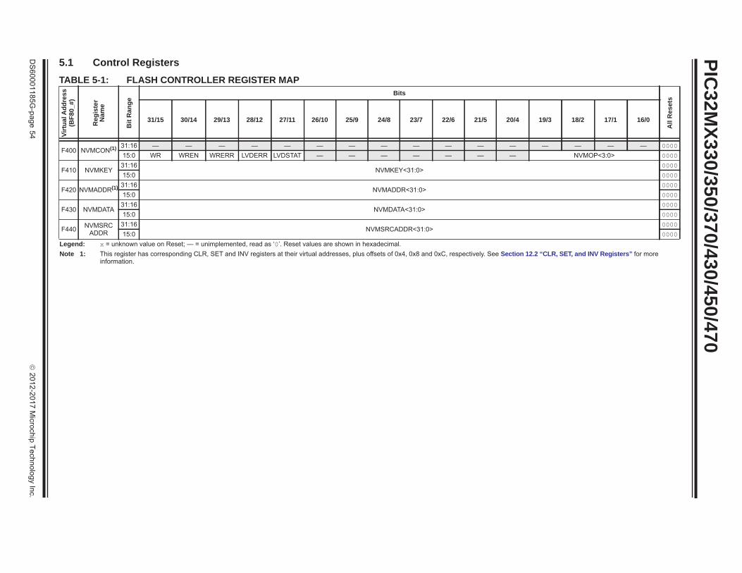
PIC32M
X330/350/370/430/450/470
DS
60001185G-page
54
2012-2017 M
icrochip Technology Inc.
5.1 Control Registers TABLE 5-1: FLASH CONTROLLER REGISTER MAP
Virt
ual A
ddre
ss(B
F80_
#)
Reg
iste
rN
ame
Bit
Ran
ge
Bits
All
Res
ets
31/15 30/14 29/13 28/12 27/11 26/10 25/9 24/8 23/7 22/6 21/5 20/4 19/3 18/2 17/1 16/0
F400 NVMCON(1) 31:16 — — — — — — — — — — — — — — — — 000015:0 WR WREN WRERR LVDERR LVDSTAT — — — — — — — NVMOP<3:0> 0000
F410 NVMKEY31:16
NVMKEY<31:0>0000
15:0 0000
F420 NVMADDR(1) 31:16NVMADDR<31:0>
000015:0 0000
F430 NVMDATA31:16
NVMDATA<31:0>0000
15:0 0000
F440 NVMSRCADDR
31:16NVMSRCADDR<31:0>
000015:0 0000
Legend: x = unknown value on Reset; — = unimplemented, read as ‘0’. Reset values are shown in hexadecimal.Note 1: This register has corresponding CLR, SET and INV registers at their virtual addresses, plus offsets of 0x4, 0x8 and 0xC, respectively. See Section 12.2 “CLR, SET, and INV Registers” for more
information.

2012-2017 Microchip Technology Inc. DS60001185G-page 55
PIC32MX330/350/370/430/450/470
REGISTER 5-1: NVMCON: PROGRAMMING CONTROL REGISTER Bit
RangeBit
31/23/15/7Bit
30/22/14/6Bit
29/21/13/5Bit
28/20/12/4Bit
27/19/11/3Bit
26/18/10/2Bit
25/17/9/1Bit
24/16/8/0
31:24U-0 U-0 U-0 U-0 U-0 U-0 U-0 U-0
— — — — — — — —
23:16U-0 U-0 U-0 U-0 U-0 U-0 U-0 U-0
— — — — — — — —
15:8R/W-0 R/W-0 R-0 R-0 R-0 U-0 U-0 U-0
WR WREN WRERR(1) LVDERR(1) LVDSTAT(1) — — —
7:0U-0 U-0 U-0 U-0 R/W-0 R/W-0 R/W-0 R/W-0
— — — — NVMOP<3:0>
Legend:R = Readable bit W = Writable bit U = Unimplemented bit, read as ‘0’-n = Value at POR ‘1’ = Bit is set ‘0’ = Bit is cleared x = Bit is unknown
bit 31-16 Unimplemented: Read as ‘0’bit 15 WR: Write Control bit
This bit is writable when WREN = 1 and the unlock sequence is followed.1 = Initiate a Flash operation. Hardware clears this bit when the operation completes0 = Flash operation complete or inactive
bit 14 WREN: Write Enable bit1 = Enable writes to WR bit and enables LVD circuit0 = Disable writes to WR bit and disables LVD circuitThis is the only bit in this register reset by a device Reset.
bit 13 WRERR: Write Error bit(1)
This bit is read-only and is automatically set by hardware.1 = Program or erase sequence did not complete successfully0 = Program or erase sequence completed normally
bit 12 LVDERR: Low-Voltage Detect Error bit (LVD circuit must be enabled)(1)
This bit is read-only and is automatically set by hardware.1 = Low-voltage detected (possible data corruption, if WRERR is set)0 = Voltage level is acceptable for programming
bit 11 LVDSTAT: Low-Voltage Detect Status bit (LVD circuit must be enabled)(1)
This bit is read-only and is automatically set, and cleared, by hardware.1 = Low-voltage event active0 = Low-voltage event NOT active
bit 10-4 Unimplemented: Read as ‘0’bit 3-0 NVMOP<3:0>: NVM Operation bits
These bits are writable when WREN = 0.1111 = Reserved•••0111 = Reserved0110 = No operation0101 = Program Flash (PFM) erase operation: erases PFM, if all pages are not write-protected0100 = Page erase operation: erases page selected by NVMADDR, if it is not write-protected0011 = Row program operation: programs row selected by NVMADDR, if it is not write-protected0010 = No operation0001 = Word program operation: programs word selected by NVMADDR, if it is not write-protected0000 = No operation
Note 1: This bit is cleared by setting NVMOP = 0000, and initiating a Flash operation (i.e., WR).

REGISTER 5-3: NVMADDR: FLASH ADDRESS REGISTER
Bit Range
Bit31/23/15/7
Bit30/22/14/6
Bit29/21/13/5
Bit28/20/12/4
Bit27/19/11/3
Bit26/18/10/2
Bit25/17/9/1
Bit24/16/8/0
31:24R/W-0 R/W-0 R/W-0 R/W-0 R/W-0 R/W-0 R/W-0 R/W-0
NVMADDR<31:24>
23:16R/W-0 R/W-0 R/W-0 R/W-0 R/W-0 R/W-0 R/W-0 R/W-0
NVMADDR<23:16>
15:8R/W-0 R/W-0 R/W-0 R/W-0 R/W-0 R/W-0 R/W-0 R/W-0
NVMADDR<15:8>
7:0R/W-0 R/W-0 R/W-0 R/W-0 R/W-0 R/W-0 R/W-0 R/W-0
NVMADDR<7:0>
Legend:R = Readable bit W = Writable bit U = Unimplemented bit, read as ‘0’-n = Value at POR ‘1’ = Bit is set ‘0’ = Bit is cleared x = Bit is unknown
bit 31-0 NVMADDR<31:0>: Flash Address bitsBulk/Chip/PFM Erase: Address is ignoredPage Erase: Address identifies the page to eraseRow Program: Address identifies the row to programWord Program: Address identifies the word to program
PIC32MX330/350/370/430/450/470
DS60001185G-page 56 2012-2017 Microchip Technology Inc.
REGISTER 5-2: NVMKEY: PROGRAMMING UNLOCK REGISTER Bit
RangeBit
31/23/15/7Bit
30/22/14/6Bit
29/21/13/5Bit
28/20/12/4Bit
27/19/11/3Bit
26/18/10/2Bit
25/17/9/1Bit
24/16/8/0
31:24W-0 W-0 W-0 W-0 W-0 W-0 W-0 W-0
NVMKEY<31:24>
23:16W-0 W-0 W-0 W-0 W-0 W-0 W-0 W-0
NVMKEY<23:16>
15:8W-0 W-0 W-0 W-0 W-0 W-0 W-0 W-0
NVMKEY<15:8>
7:0W-0 W-0 W-0 W-0 W-0 W-0 W-0 W-0
NVMKEY<7:0>
Legend:R = Readable bit W = Writable bit U = Unimplemented bit, read as ‘0’-n = Value at POR ‘1’ = Bit is set ‘0’ = Bit is cleared x = Bit is unknown
bit 31-0 NVMKEY<31:0>: Unlock Register bitsThese bits are write-only, and read as ‘0’ on any read
Note: This register is used as part of the unlock sequence to prevent inadvertent writes to the PFM.

REGISTER 5-5: NVMSRCADDR: SOURCE DATA ADDRESS REGISTERBit
RangeBit
31/23/15/7Bit
30/22/14/6Bit
29/21/13/5Bit
28/20/12/4Bit
27/19/11/3Bit
26/18/10/2Bit
25/17/9/1Bit
24/16/8/0
31:24R/W-0 R/W-0 R/W-0 R/W-0 R/W-0 R/W-0 R/W-0 R/W-0
NVMSRCADDR<31:24>
23:16R/W-0 R/W-0 R/W-0 R/W-0 R/W-0 R/W-0 R/W-0 R/W-0
NVMSRCADDR<23:16>
15:8R/W-0 R/W-0 R/W-0 R/W-0 R/W-0 R/W-0 R/W-0 R/W-0
NVMSRCADDR<15:8>
7:0R/W-0 R/W-0 R/W-0 R/W-0 R/W-0 R/W-0 R/W-0 R/W-0
NVMSRCADDR<7:0>
Legend:R = Readable bit W = Writable bit U = Unimplemented bit, read as ‘0’-n = Value at POR ‘1’ = Bit is set ‘0’ = Bit is cleared x = Bit is unknown
bit 31-0 NVMSRCADDR<31:0>: Source Data Address bitsThe system physical address of the data to be programmed into the Flash when the NVMOP<3:0> bits (NVMCON<3:0>) are set to perform row programming.
2012-2017 Microchip Technology Inc. DS60001185G-page 57
PIC32MX330/350/370/430/450/470
REGISTER 5-4: NVMDATA: FLASH PROGRAM DATA REGISTER Bit
RangeBit
31/23/15/7Bit
30/22/14/6Bit
29/21/13/5Bit
28/20/12/4Bit
27/19/11/3Bit
26/18/10/2Bit
25/17/9/1Bit
24/16/8/0
31:24R/W-0 R/W-0 R/W-0 R/W-0 R/W-0 R/W-0 R/W-0 R/W-0
NVMDATA<31:24>
23:16R/W-0 R/W-0 R/W-0 R/W-0 R/W-0 R/W-0 R/W-0 R/W-0
NVMDATA<23:16>
15:8R/W-0 R/W-0 R/W-0 R/W-0 R/W-0 R/W-0 R/W-0 R/W-0
NVMDATA<15:8>
7:0R/W-0 R/W-0 R/W-0 R/W-0 R/W-0 R/W-0 R/W-0 R/W-0
NVMDATA<7:0>
Legend:R = Readable bit W = Writable bit U = Unimplemented bit, read as ‘0’-n = Value at POR ‘1’ = Bit is set ‘0’ = Bit is cleared x = Bit is unknown
bit 31-0 NVMDATA<31:0>: Flash Programming Data bits
Note: The bits in this register are only reset by a Power-on Reset (POR).

PIC32MX330/350/370/430/450/470
DS60001185G-page 58 2012-2017 Microchip Technology Inc.
NOTES:

2012-2017 Microchip Technology Inc. DS60001185G-page 59
PIC32MX330/350/370/430/450/4706.0 RESETS
Note: This data sheet summarizes the features of the PIC32MX330/350/370/430/450/470 family of devices. It is not intended to be a comprehensive reference source. To complement the information in this data sheet, refer to Section 7. “Resets”(DS60001118), which is available from the Documentation > Reference Manual section of the Microchip PIC32 web site (www.microchip.com/pic32).
The Reset module combines all Reset sources and controls the device Master Reset signal, SYSRST. The following is a list of device Reset sources:
• POR: Power-on Reset • MCLR: Master Clear Reset pin • SWR: Software Reset• WDTR: Watchdog Timer Reset• BOR: Brown-out Reset• CMR: Configuration Mismatch Reset• HVDR: High Voltage Detect Reset
A simplified block diagram of the Reset module is illustrated in Figure 6-1.
FIGURE 6-1: SYSTEM RESET BLOCK DIAGRAM
MCLR
VDDVDD Rise
Detect
POR
Sleep or Idle
Brown-outReset
WDTTime-out
Glitch Filter
BOR
Configuration
SYSRST
Software Reset
Power-upTimer
Voltage
Enabled
Reset
WDTR
SWRCMR
MCLR
Mismatch
Regulator
Brown-outReset
HVDRVCAP
HVD Detectand Reset

PIC32M
X330/350/370/430/450/470
DS
60001185G-page
60
2012-2017 M
icrochip Technology Inc.
6.1 Reset Control RegistersTABLE 6-1: SYSTEM CONTROL REGISTER MAP
Virt
ual A
ddre
ss(B
F80_
#)
Reg
iste
rN
ame(1
)
Bit
Ran
ge
Bits
All
Res
ets
31/15 30/14 29/13 28/12 27/11 26/10 25/9 24/8 23/7 22/6 21/5 20/4 19/3 18/2 17/1 16/0
F600 RCON31:16 — — HVDR — — — — — — — — — — — — — 000015:0 — — — — — — CMR VREGS EXTR SWR — WDTO SLEEP IDLE BOR POR xxxx(2)
F610 RSWRST31:16 — — — — — — — — — — — — — — — — 000015:0 — — — — — — — — — — — — — — — SWRST 0000
Legend: x = unknown value on Reset; — = unimplemented, read as ‘0’. Reset values are shown in hexadecimal.Note 1: All registers in this table have corresponding CLR, SET and INV registers at their virtual addresses, plus offsets of 0x4, 0x8 and 0xC, respectively. See Section 12.2 “CLR, SET, and INV Registers” for
more information.2: Reset values are dependent on the DEVCFGx Configuration bits and the type of reset.

2012-2017 Microchip Technology Inc. DS60001185G-page 61
PIC32MX330/350/370/430/450/470
REGISTER 6-1: RCON: RESET CONTROL REGISTERBit
RangeBit
31/23/15/7Bit
30/22/14/6Bit
29/21/13/5Bit
28/20/12/4Bit
27/19/11/3Bit
26/18/10/2Bit
25/17/9/1Bit
24/16/8/0
31:24U-0 U-0 R/W-0 U-0 U-0 U-0 U-0 U-0
— — HVDR — — — — —
23:16U-0 U-0 U-0 U-0 U-0 U-0 U-0 U-0
— — — — — — — —
15:8U-0 U-0 U-0 U-0 U-0 U-0 R/W-0, HS R/W-0
— — — — — — CMR VREGS
7:0R/W-0, HS R/W-0, HS U-0 R/W-0, HS R/W-0, HS R/W-0, HS R/W-1, HS R/W-1, HS
EXTR SWR — WDTO SLEEP IDLE BOR(1) POR(1)
Legend: HS = Set by hardwareR = Readable bit W = Writable bit U = Unimplemented bit, read as ‘0’-n = Value at POR ‘1’ = Bit is set ‘0’ = Bit is cleared x = Bit is unknown
bit 31-30 Unimplemented: Read as ‘0’bit 29 HVDR: High Voltage Detect Reset Flag bit
1 = High Voltage Detect (HVD) Reset has occurred0 = HVD Reset has not occurred
bit 28-10 Unimplemented: Read as ‘0’bit 9 CMR: Configuration Mismatch Reset Flag bit
1 = Configuration mismatch Reset has occurred0 = Configuration mismatch Reset has not occurred
bit 8 VREGS: Voltage Regulator Standby Enable bit1 = Regulator is enabled and is on during Sleep mode0 = Regulator is set to Stand-by Tracking mode
bit 7 EXTR: External Reset (MCLR) Pin Flag bit1 = Master Clear (pin) Reset has occurred0 = Master Clear (pin) Reset has not occurred
bit 6 SWR: Software Reset Flag bit1 = Software Reset was executed0 = Software Reset as not executed
bit 5 Unimplemented: Read as ‘0’bit 4 WDTO: Watchdog Timer Time-out Flag bit
1 = WDT Time-out has occurred0 = WDT Time-out has not occurred
bit 3 SLEEP: Wake From Sleep Flag bit1 = Device was in Sleep mode0 = Device was not in Sleep mode
bit 2 IDLE: Wake From Idle Flag bit1 = Device was in Idle mode0 = Device was not in Idle mode
bit 1 BOR: Brown-out Reset Flag bit(1)
1 = Brown-out Reset has occurred 0 = Brown-out Reset has not occurred
bit 0 POR: Power-on Reset Flag bit(1)
1 = Power-on Reset has occurred0 = Power-on Reset has not occurred
Note 1: User software must clear this bit to view next detection.

PIC32MX330/350/370/430/450/470
DS60001185G-page 62 2012-2017 Microchip Technology Inc.
REGISTER 6-2: RSWRST: SOFTWARE RESET REGISTERBit
RangeBit
31/23/15/7Bit
30/22/14/6Bit
29/21/13/5Bit
28/20/12/4Bit
27/19/11/3Bit
26/18/10/2Bit
25/17/9/1Bit
24/16/8/0
31:24U-0 U-0 U-0 U-0 U-0 U-0 U-0 U-0
— — — — — — — —
23:16U-0 U-0 U-0 U-0 U-0 U-0 U-0 U-0
— — — — — — — —
15:8U-0 U-0 U-0 U-0 U-0 U-0 U-0 U-0
— — — — — — — —
7:0U-0 U-0 U-0 U-0 U-0 U-0 U-0 W-0, HC
— — — — — — — SWRST(1)
Legend: HC = Cleared by hardwareR = Readable bit W = Writable bit U = Unimplemented bit, read as ‘0’-n = Value at POR ‘1’ = Bit is set ‘0’ = Bit is cleared x = Bit is unknown
bit 31-1 Unimplemented: Read as ‘0’bit 0 SWRST: Software Reset Trigger bit(1)
1 = Enable software Reset event0 = No effect
Note 1: The system unlock sequence must be performed before the SWRST bit can be written. Refer to Section 6. “Oscillator” (DS60001112) in the “PIC32 Family Reference Manual” for details.

2012-2017 Microchip Technology Inc. DS60001185G-page 63
PIC32MX330/350/370/430/450/4707.0 INTERRUPT CONTROLLER
Note: This data sheet summarizes the features of the PIC32MX330/350/370/430/450/470 family of devices. It is not intended to be a comprehensive reference source. To complement the information in this data sheet, refer to Section 8. “Interrupt Con-troller” (DS60001108), which is available from the Documentation > Reference Manual section of the Microchip PIC32 web site (www.microchip.com/pic32).
PIC32MX330/350/370/430/450/470 devices generate interrupt requests in response to interrupt events from peripheral modules. The interrupt control module exists externally to the CPU logic and prioritizes the interrupt events before presenting them to the CPU.
The PIC32MX330/350/370/430/450/470 interrupt module includes the following features:
• Up to 76 interrupt sources• Up to 46 interrupt vectors• Single and multi-vector mode operations• Five external interrupts with edge polarity control• Interrupt proximity timer• Seven user-selectable priority levels for each
vector• Four user-selectable subpriority levels within each
priority• Dedicated shadow set configurable for any priority level
(see the FSRSSEL<2:0> bits (DEVCFG3<18:16>) in 28.0 “Special Features” for more information)
• Software can generate any interrupt• User-configurable interrupt vector table location• User-configurable interrupt vector spacing
FIGURE 7-1: INTERRUPT CONTROLLER MODULE BLOCK DIAGRAM
Interrupt Controller
Inte
rrup
t Req
uest
s Vector Number
CPU CorePriority Level
Shadow Set Number

PIC32MX330/350/370/430/450/470
DS60001185G-page 64 2012-2017 Microchip Technology Inc.
TABLE 7-1: INTERRUPT IRQ, VECTOR AND BIT LOCATION
Interrupt Source(1) IRQ # Vector #
Interrupt Bit Location Persistent InterruptFlag Enable Priority Sub-priority
Highest Natural Order PriorityCT – Core Timer Interrupt 0 0 IFS0<0> IEC0<0> IPC0<4:2> IPC0<1:0> NoCS0 – Core Software Interrupt 0 1 1 IFS0<1> IEC0<1> IPC0<12:10> IPC0<9:8> NoCS1 – Core Software Interrupt 1 2 2 IFS0<2> IEC0<2> IPC0<20:18> IPC0<17:16> NoINT0 – External Interrupt 3 3 IFS0<3> IEC0<3> IPC0<28:26> IPC0<25:24> NoT1 – Timer1 4 4 IFS0<4> IEC0<4> IPC1<4:2> IPC1<1:0> NoIC1E – Input Capture 1 Error 5 5 IFS0<5> IEC0<5> IPC1<12:10> IPC1<9:8> YesIC1 – Input Capture 1 6 5 IFS0<6> IEC0<6> IPC1<12:10> IPC1<9:8> YesOC1 – Output Compare 1 7 6 IFS0<7> IEC0<7> IPC1<20:18> IPC1<17:16> NoINT1 – External Interrupt 1 8 7 IFS0<8> IEC0<8> IPC1<28:26> IPC1<25:24> NoT2 – Timer2 9 8 IFS0<9> IEC0<9> IPC2<4:2> IPC2<1:0> NoIC2E – Input Capture 2 10 9 IFS0<10> IEC0<10> IPC2<12:10> IPC2<9:8> YesIC2 – Input Capture 2 11 9 IFS0<11> IEC0<11> IPC2<12:10> IPC2<9:8> YesOC2 – Output Compare 2 12 10 IFS0<12> IEC0<12> IPC2<20:18> IPC2<17:16> NoINT2 – External Interrupt 2 13 11 IFS0<13> IEC0<13> IPC2<28:26> IPC2<25:24> NoT3 – Timer3 14 12 IFS0<14> IEC0<14> IPC3<4:2> IPC3<1:0> NoIC3E – Input Capture 3 15 13 IFS0<15> IEC0<15> IPC3<12:10> IPC3<9:8> YesIC3 – Input Capture 3 16 13 IFS0<16> IEC0<16> IPC3<12:10> IPC3<9:8> YesOC3 – Output Compare 3 17 14 IFS0<17> IEC0<17> IPC3<20:18> IPC3<17:16> NoINT3 – External Interrupt 3 18 15 IFS0<18> IEC0<18> IPC3<28:26> IPC3<25:24> NoT4 – Timer4 19 16 IFS0<19> IEC0<19> IPC4<4:2> IPC4<1:0> NoIC4E – Input Capture 4 Error 20 17 IFS0<20> IEC0<20> IPC4<12:10> IPC4<9:8> YesIC4 – Input Capture 4 21 17 IFS0<21> IEC0<21> IPC4<12:10> IPC4<9:8> YesOC4 – Output Compare 4 22 18 IFS0<22> IEC0<22> IPC4<20:18> IPC4<17:16> NoINT4 – External Interrupt 4 23 19 IFS0<23> IEC0<23> IPC4<28:26> IPC4<25:24> NoT5 – Timer5 24 20 IFS0<24> IEC0<24> IPC5<4:2> IPC5<1:0> NoIC5E – Input Capture 5 Error 25 21 IFS0<25> IEC0<25> IPC5<12:10> IPC5<9:8> YesIC5 – Input Capture 5 26 21 IFS0<26> IEC0<26> IPC5<12:10> IPC5<9:8> YesOC5 – Output Compare 5 27 22 IFS0<27> IEC0<27> IPC5<20:18> IPC5<17:16> NoAD1 – ADC1 Convert done 28 23 IFS0<28> IEC0<28> IPC5<28:26> IPC5<25:24> YesFSCM – Fail-Safe Clock Monitor 29 24 IFS0<29> IEC0<29> IPC6<4:2> IPC6<1:0> NoRTCC – Real-Time Clock and Calendar 30 25 IFS0<30> IEC0<30> IPC6<12:10> IPC6<9:8> NoFCE – Flash Control Event 31 26 IFS0<31> IEC0<31> IPC6<20:18> IPC6<17:16> NoCMP1 – Comparator Interrupt 32 27 IFS1<0> IEC1<0> IPC6<28:26> IPC6<25:24> NoCMP2 – Comparator Interrupt 33 28 IFS1<1> IEC1<1> IPC7<4:2> IPC7<1:0> NoUSB – USB Interrupts 34 29 IFS1<2> IEC1<2> IPC7<12:10> IPC7<9:8> YesSPI1E – SPI1 Fault 35 30 IFS1<3> IEC1<3> IPC7<20:18> IPC7<17:16> YesSPI1RX – SPI1 Receive Done 36 30 IFS1<4> IEC1<4> IPC7<20:18> IPC7<17:16> YesSPI1TX – SPI1 Transfer Done 37 30 IFS1<5> IEC1<5> IPC7<20:18> IPC7<17:16> YesU1E – UART1 Fault 38 31 IFS1<6> IEC1<6> IPC7<28:26> IPC7<25:24> YesU1RX – UART1 Receive Done 39 31 IFS1<7> IEC1<7> IPC7<28:26> IPC7<25:24> YesU1TX – UART1 Transfer Done 40 31 IFS1<8> IEC1<8> IPC7<28:26> IPC7<25:24> YesI2C1B – I2C1 Bus Collision Event 41 32 IFS1<9> IEC1<9> IPC8<4:2> IPC8<1:0> YesI2C1S – I2C1 Slave Event 42 32 IFS1<10> IEC1<10> IPC8<4:2> IPC8<1:0> YesI2C1M – I2C1 Master Event 43 32 IFS1<11> IEC1<11> IPC8<4:2> IPC8<1:0> YesCNA – PORTA Input Change Interrupt 44 33 IFS1<12> IEC1<12> IPC8<12:10> IPC8<9:8> YesNote 1: Not all interrupt sources are available on all devices. See TABLE 1: “PIC32MX330/350/370/430/450/470 Controller
Family Features” for the list of available peripherals.

2012-2017 Microchip Technology Inc. DS60001185G-page 65
PIC32MX330/350/370/430/450/470
CNB – PORTB Input Change Interrupt 45 33 IFS1<13> IEC1<13> IPC8<12:10> IPC8<9:8> YesCNC – PORTC Input Change Interrupt 46 33 IFS1<14> IEC1<14> IPC8<12:10> IPC8<9:8> YesCND – PORTD Input Change Interrupt 47 33 IFS1<15> IEC1<15> IPC8<12:10> IPC8<9:8> YesCNE – PORTE Input Change Interrupt 48 33 IFS1<16> IEC1<16> IPC8<12:10> IPC8<9:8> YesCNF – PORTF Input Change Interrupt 49 33 IFS1<17> IEC1<17> IPC8<12:10> IPC8<9:8> YesCNG – PORTG Input Change Interrupt 50 33 IFS1<18> IEC1<18> IPC8<12:10> IPC8<9:8> YesPMP – Parallel Master Port 51 34 IFS1<19> IEC1<19> IPC8<20:18> IPC8<17:16> YesPMPE – Parallel Master Port Error 52 34 IFS1<20> IEC1<20> IPC8<20:18> IPC8<17:16> YesSPI2E – SPI2 Fault 53 35 IFS1<21> IEC1<21> IPC8<28:26> IPC8<25:24> YesSPI2RX – SPI2 Receive Done 54 35 IFS1<22> IEC1<22> IPC8<28:26> IPC8<25:24> YesSPI2TX – SPI2 Transfer Done 55 35 IFS1<23> IEC1<23> IPC8<28:26> IPC8<25:24> YesU2E – UART2 Error 56 36 IFS1<24> IEC1<24> IPC9<4:2> IPC9<1:0> YesU2RX – UART2 Receiver 57 36 IFS1<25> IEC1<25> IPC9<4:2> IPC9<1:0> YesU2TX – UART2 Transmitter 58 36 IFS1<26> IEC1<26> IPC9<4:2> IPC9<1:0> YesI2C2B – I2C2 Bus Collision Event 59 37 IFS1<27> IEC1<27> IPC9<12:10> IPC9<9:8> YesI2C2S – I2C2 Slave Event 60 37 IFS1<28> IEC1<28> IPC9<12:10> IPC9<9:8> YesI2C2M – I2C2 Master Event 61 37 IFS1<29> IEC1<29> IPC9<12:10> IPC9<9:8> YesU3E – UART3 Error 62 38 IFS1<30> IEC1<30> IPC9<20:18> IPC9<17:16> YesU3RX – UART3 Receiver 63 38 IFS1<31> IEC1<31> IPC9<20:18> IPC9<17:16> YesU3TX – UART3 Transmitter 64 38 IFS2<0> IEC2<0> IPC9<20:18> IPC9<17:16> YesU4E – UART4 Error 65 39 IFS2<1> IEC2<1> IPC9<28:26> IPC9<25:24> YesU4RX – UART4 Receiver 66 39 IFS2<2> IEC2<2> IPC9<28:26> IPC9<25:24> YesU4TX – UART4 Transmitter 67 39 IFS2<3> IEC2<3> IPC9<28:26> IPC9<25:24> YesU5E – UART5 Error 68 40 IFS2<4> IEC2<4> IPC10<4:2> IPC10<1:0> YesU5RX – UART5 Receiver 69 40 IFS2<5> IEC2<5> IPC10<4:2> IPC10<1:0> YesU5TX – UART5 Transmitter 70 40 IFS2<6> IEC2<6> IPC10<4:2> IPC10<1:0> YesCTMU – CTMU Event 71 41 IFS2<7> IEC2<7> IPC10<12:10> IPC10<9:8> YesDMA0 – DMA Channel 0 72 42 IFS2<8> IEC2<8> IPC10<20:18> IPC10<17:16> NoDMA1 – DMA Channel 1 73 43 IFS2<9> IEC2<9> IPC10<28:26> IPC10<25:24> NoDMA2 – DMA Channel 2 74 44 IFS2<10> IEC2<10> IPC11<4:2> IPC11<1:0> NoDMA3 – DMA Channel 3 75 45 IFS2<11> IEC2<11> IPC11<12:10> IPC11<9:8> No
Lowest Natural Order Priority
TABLE 7-1: INTERRUPT IRQ, VECTOR AND BIT LOCATION (CONTINUED)
Interrupt Source(1) IRQ # Vector #
Interrupt Bit Location Persistent InterruptFlag Enable Priority Sub-priority
Note 1: Not all interrupt sources are available on all devices. See TABLE 1: “PIC32MX330/350/370/430/450/470 Controller Family Features” for the list of available peripherals.

PIC32M
X330/350/370/430/450/470
DS
60001185G-page
66
2012-2017 M
icrochip Technology Inc.
7.1 Interrupts Control Registers TABLE 7-2: INTERRUPT REGISTER MAP
Virtu
al A
ddre
ss(B
F88_
#)
Reg
iste
rN
ame
Bit
Ran
ge
Bits
All
Res
ets
31/15 30/14 29/13 28/12 27/11 26/10 25/9 24/8 23/7 22/6 21/5 20/4 19/3 18/2 17/1 16/0
1000 INTCON31:16 — — — — — — — — — — — — — — — SS0 0000
15:0 — — — MVEC — TPC<2:0> — — — INT4EP INT3EP INT2EP INT1EP INT0EP 0000
1010 INTSTAT31:16 — — — — — — — — — — — — — — — — 0000
15:0 — — — — — SRIPL<2:0> — — VEC<5:0> 0000
1020 IPTMR31:16
IPTMR<31:0>0000
15:0 0000
1030 IFS031:16 FCEIF RTCCIF FSCMIF AD1IF OC5IF IC5IF IC5EIF T5IF INT4IF OC4IF IC4IF IC4EIF T4IF INT3IF OC3IF IC3IF 0000
15:0 IC3EIF T3IF INT2IF OC2IF IC2IF IC2EIF T2IF INT1IF OC1IF IC1IF IC1EIF T1IF INT0IF CS1IF CS0IF CTIF 0000
1040 IFS131:16 U3RXIF U3EIF I2C2MIF I2C2SIF I2C2BIF U2TXIF U2RXIF U2EIF SPI2TXIF SPI2RXIF SPI2EIF PMPEIF PMPIF CNGIF CNFIF CNEIF 0000
15:0 CNDIF CNCIF CNBIF CNAIF I2C1MIF I2C1SIF I2C1BIF U1TXIF U1RXIF U1EIF SPI1TXIF SPI1RXIF SPI1EIF USBIF(2) CMP2IF CMP1IF 0000
1050 IFS231:16 — — — — — — — — — — — — — — — — 0000
15:0 — — — — DMA3IF DMA2IF DMA1IF DMA0IF CTMUIF U5TXIF(1) U5RXIF(1) U5EIF(1) U4TXIF U4RXIF U4EIF U3TXIF 0000
1060 IEC031:16 FCEIE RTCCIE FSCMIE AD1IE OC5IE IC5IE IC5EIE T5IE INT4IE OC4IE IC4IE IC4EIE T4IE INT3IE OC3IE IC3IE 0000
15:0 IC3EIE T3IE INT2IE OC2IE IC2IE IC2EIE T2IE INT1IE OC1IE IC1IE IC1EIE T1IE INT0IE CS1IE CS0IE CTIE 0000
1070 IEC131:16 U3RXIE U3EIE I2C2MIE I2C2SIE I2C2BIE U2TXIE U2RXIE U2EIE SPI2TXIE SPI2RXIE SPI2EIE PMPEIE PMPIE CNGIE CNFIE CNEIE 0000
15:0 CNDIE CNCIE CNBIE CNAIE I2C1MIE I2C1SIE I2C1BIE U1TXIE U1RXIE U1EIE SPI1TXIE SPI1RXIE SPI1EIE USBIE(2) CMP2IE CMP1IE 0000
1080 IEC231:16 — — — — — — — — — — — — — — — — 0000
15:0 — — — — DMA3IE DMA2IE DMA1IE DMA0IE CTMUIE U5TXIE(1) U5RXIE(1) U5EIE(1) U4TXIE U4RXIE U4EIE U3TXIE 0000
1090 IPC031:16 — — — INT0IP<2:0> INT0IS<1:0> — — — CS1IP<2:0> CS1IS<1:0> 0000
15:0 — — — CS0IP<2:0> CS0IS<1:0> — — — CTIP<2:0> CTIS<1:0> 0000
10A0 IPC131:16 — — — INT1IP<2:0> INT1IS<1:0> — — — OC1IP<2:0> OC1IS<1:0> 0000
15:0 — — — IC1IP<2:0> IC1IS<1:0> — — — T1IP<2:0> T1IS<1:0> 0000
10B0 IPC231:16 — — — INT2IP<2:0> INT2IS<1:0> — — — OC2IP<2:0> OC2IS<1:0> 0000
15:0 — — — IC2IP<2:0> IC2IS<1:0> — — — T2IP<2:0> T2IS<1:0> 0000
10C0 IPC331:16 — — — INT3IP<2:0> INT3IS<1:0> — — — OC3IP<2:0> OC3IS<1:0> 0000
15:0 — — — IC3IP<2:0> IC3IS<1:0> — — — T3IP<2:0> T3IS<1:0> 0000
10D0 IPC431:16 — — — INT4IP<2:0> INT4IS<1:0> — — — OC4IP<2:0> OC4IS<1:0> 0000
15:0 — — — IC4IP<2:0> IC4IS<1:0> — — — T4IP<2:0> T4IS<1:0> 0000
10E0 IPC531:16 — — — AD1IP<2:0> AD1IS<1:0> — — — OC5IP<2:0> OC5IS<1:0> 0000
15:0 — — — IC5IP<2:0> IC5IS<1:0> — — — T5IP<2:0> T5IS<1:0> 0000
Legend: x = unknown value on Reset; — = unimplemented, read as ‘0’. Reset values are shown in hexadecimal.Note 1: This bit is only available on 100-pin devices.
2: This bit is only implemented on devices with a USB module.

2012-2017 M
icrochip Technology Inc.D
S60001185G
-page
67
PIC32M
X330/350/370/430/450/470
10F0 IPC631:16 — — — CMP1IP<2:0> CMP1IS<1:0> — — — FCEIP<2:0> FCEIS<1:0> 0000
15:0 — — — RTCCIP<2:0> RTCCIS<1:0> — — — FSCMIP<2:0> FSCMIS<1:0> 0000
1100 IPC731:16 — — — U1IP<2:0> U1IS<1:0> — — — SPI1IP<2:0> SPI1IS<1:0> 0000
15:0 — — — USBIP<2:0>(2) USBIS<1:0>(2) — — — CMP2IP<2:0> CMP2IS<1:0> 0000
1110 IPC831:16 — — — SPI2IP<2:0> SPI2IS<1:0> — — — PMPIP<2:0> PMPIS<1:0> 0000
15:0 — — — CNIP<2:0> CNIS<1:0> — — — I2C1IP<2:0> I2C1IS<1:0> 0000
1120 IPC931:16 — — — U4IP<2:0> U4IS<1:0> — — — U3IP<2:0> U3IS<1:0> 0000
15:0 — — — I2C2IP<2:0> I2C2IS<1:0> — — — U2IP<2:0> U2IS<1:0> 0000
1130 IPC1031:16 — — — DMA1IP<2:0> DMA1IS<1:0> — — — DMA0IP<2:0> DMA0IS<1:0> 0000
15:0 — — — CTMUIP<2:0> CTMUIS<1:0> — — — U5IP<2:0> U5IS<1:0> 0000
1140 IPC1131:16 — — — — — — — — — — — — — — — — 0000
15:0 — — — DMA3IP<2:0> DMA3IS<1:0> — — — DMA2IP<2:0> DMA2IS<1:0> 0000
TABLE 7-2: INTERRUPT REGISTER MAP (CONTINUED)Vi
rtual
Add
ress
(BF8
8_#)
Reg
iste
rN
ame
Bit
Ran
ge
Bits
All
Res
ets
31/15 30/14 29/13 28/12 27/11 26/10 25/9 24/8 23/7 22/6 21/5 20/4 19/3 18/2 17/1 16/0
Legend: x = unknown value on Reset; — = unimplemented, read as ‘0’. Reset values are shown in hexadecimal.Note 1: This bit is only available on 100-pin devices.
2: This bit is only implemented on devices with a USB module.

PIC32MX330/350/370/430/450/470
DS60001185G-page 68 2012-2017 Microchip Technology Inc.
REGISTER 7-1: INTCON: INTERRUPT CONTROL REGISTERBit
RangeBit
31/23/15/7Bit
30/22/14/6Bit
29/21/13/5Bit
28/20/12/4Bit
27/19/11/3Bit
26/18/10/2Bit
25/17/9/1Bit
24/16/8/0
31:24U-0 U-0 U-0 U-0 U-0 U-0 U-0 U-0
— — — — — — — —
23:16U-0 U-0 U-0 U-0 U-0 U-0 U-0 R/W-0
— — — — — — — SS0
15:8U-0 U-0 U-0 R/W-0 U-0 R/W-0 R/W-0 R/W-0
— — — MVEC — TPC<2:0>
7:0U-0 U-0 U-0 R/W-0 R/W-0 R/W-0 R/W-0 R/W-0
— — — INT4EP INT3EP INT2EP INT1EP INT0EP
Legend:R = Readable bit W = Writable bit U = Unimplemented bit, read as ‘0’-n = Value at POR ‘1’ = Bit is set ‘0’ = Bit is cleared x = Bit is unknown
bit 31-17 Unimplemented: Read as ‘0’bit 16 SS0: Single Vector Shadow Register Set bit
1 = Single vector is presented with a shadow register set0 = Single vector is not presented with a shadow register set
bit 15-13 Unimplemented: Read as ‘0’bit 12 MVEC: Multi Vector Configuration bit
1 = Interrupt controller configured for multi vectored mode0 = Interrupt controller configured for single vectored mode
bit 11 Unimplemented: Read as ‘0’bit 10-8 TPC<2:0>: Interrupt Proximity Timer Control bits
111 = Interrupts of group priority 7 or lower start the Interrupt Proximity timer110 = Interrupts of group priority 6 or lower start the Interrupt Proximity timer101 = Interrupts of group priority 5 or lower start the Interrupt Proximity timer100 = Interrupts of group priority 4 or lower start the Interrupt Proximity timer011 = Interrupts of group priority 3 or lower start the Interrupt Proximity timer010 = Interrupts of group priority 2 or lower start the Interrupt Proximity timer001 = Interrupts of group priority 1 start the Interrupt Proximity timer000 = Disables Interrupt Proximity timer
bit 7-5 Unimplemented: Read as ‘0’bit 4 INT4EP: External Interrupt 4 Edge Polarity Control bit
1 = Rising edge0 = Falling edge
bit 3 INT3EP: External Interrupt 3 Edge Polarity Control bit1 = Rising edge0 = Falling edge
bit 2 INT2EP: External Interrupt 2 Edge Polarity Control bit1 = Rising edge0 = Falling edge
bit 1 INT1EP: External Interrupt 1 Edge Polarity Control bit1 = Rising edge0 = Falling edge
bit 0 INT0EP: External Interrupt 0 Edge Polarity Control bit1 = Rising edge0 = Falling edge

REGISTER 7-3: IPTMR: INTERRUPT PROXIMITY TIMER REGISTERBit
RangeBit
31/23/15/7Bit
30/22/14/6Bit
29/21/13/5Bit
28/20/12/4Bit
27/19/11/3Bit
26/18/10/2Bit
25/17/9/1Bit
24/16/8/0
31:24R/W-0 R/W-0 R/W-0 R/W-0 R/W-0 R/W-0 R/W-0 R/W-0
IPTMR<31:24>
23:16R/W-0 R/W-0 R/W-0 R/W-0 R/W-0 R/W-0 R/W-0 R/W-0
IPTMR<23:16>
15:8R/W-0 R/W-0 R/W-0 R/W-0 R/W-0 R/W-0 R/W-0 R/W-0
IPTMR<15:8>
7:0R/W-0 R/W-0 R/W-0 R/W-0 R/W-0 R/W-0 R/W-0 R/W-0
IPTMR<7:0>
Legend:R = Readable bit W = Writable bit U = Unimplemented bit, read as ‘0’-n = Value at POR ‘1’ = Bit is set ‘0’ = Bit is cleared x = Bit is unknown
IPTMR<31:0>: Interrupt Proximity Timer Reload bitsUsed by the Interrupt Proximity Timer as a reload value when the Interrupt Proximity timer is triggered by an interrupt event.
2012-2017 Microchip Technology Inc. DS60001185G-page 69
PIC32MX330/350/370/430/450/470
REGISTER 7-2: INTSTAT: INTERRUPT STATUS REGISTERBit
RangeBit
31/23/15/7Bit
30/22/14/6Bit
29/21/13/5Bit
28/20/12/4Bit
27/19/11/3Bit
26/18/10/2Bit
25/17/9/1Bit
24/16/8/0
31:24U-0 U-0 U-0 U-0 U-0 U-0 U-0 U-0
— — — — — — — —
23:16U-0 U-0 U-0 U-0 U-0 U-0 U-0 U-0
— — — — — — — —
15:8U-0 U-0 U-0 U-0 U-0 R/W-0 R/W-0 R/W-0
— — — — — SRIPL<2:0>(1)
7:0U-0 U-0 R/W-0 R/W-0 R/W-0 R/W-0 R/W-0 R/W-0
— — VEC<5:0>(1)
Legend:R = Readable bit W = Writable bit U = Unimplemented bit, read as ‘0’-n = Value at POR ‘1’ = Bit is set ‘0’ = Bit is cleared x = Bit is unknown
bit 31-11 Unimplemented: Read as ‘0’bit 10-8 SRIPL<2:0>: Requested Priority Level bits(1)
111-000 = The priority level of the latest interrupt presented to the CPUbit 7-6 Unimplemented: Read as ‘0’bit 5-0 VEC<5:0>: Interrupt Vector bits(1)
11111-00000 = The interrupt vector that is presented to the CPU
Note 1: This value should only be used when the interrupt controller is configured for Single Vector mode.
bit 31-0

REGISTER 7-5: IECx: INTERRUPT ENABLE CONTROL REGISTERBit
RangeBit
31/23/15/7Bit
30/22/14/6Bit
29/21/13/5Bit
28/20/12/4Bit
27/19/11/3Bit
26/18/10/2Bit
25/17/9/1Bit
24/16/8/0
31:24R/W-0 R/W-0 R/W-0 R/W-0 R/W-0 R/W-0 R/W-0 R/W-0
IEC31 IEC30 IEC29 IEC28 IEC27 IEC26 IEC25 IEC24
23:16R/W-0 R/W-0 R/W-0 R/W-0 R/W-0 R/W-0 R/W-0 R/W-0
IEC23 IEC22 IEC21 IEC20 IEC19 IEC18 IEC17 IEC16
15:8R/W-0 R/W-0 R/W-0 R/W-0 R/W-0 R/W-0 R/W-0 R/W-0
IEC15 IEC14 IEC13 IEC12 IEC11 IEC10 IEC9 IEC8
7:0R/W-0 R/W-0 R/W-0 R/W-0 R/W-0 R/W-0 R/W-0 R/W-0
IEC7 IEC6 IEC5 IEC4 IEC3 IEC2 IEC1 IEC0
Legend:R = Readable bit W = Writable bit U = Unimplemented bit, read as ‘0’-n = Value at POR ‘1’ = Bit is set ‘0’ = Bit is cleared x = Bit is unknown
IEC31-IEC0: Interrupt Enable bits1 = Interrupt is enabled0 = Interrupt is disabled
Note: This register represents a generic definition of the IECx register. Refer to Table 7-1 for the exact bit definitions.
PIC32MX330/350/370/430/450/470
DS60001185G-page 70 2012-2017 Microchip Technology Inc.
REGISTER 7-4: IFSx: INTERRUPT FLAG STATUS REGISTERBit
RangeBit
31/23/15/7Bit
30/22/14/6Bit
29/21/13/5Bit
28/20/12/4Bit
27/19/11/3Bit
26/18/10/2Bit
25/17/9/1Bit
24/16/8/0
31:24R/W-0 R/W-0 R/W-0 R/W-0 R/W-0 R/W-0 R/W-0 R/W-0
IFS31 IFS30 IFS29 IFS28 IFS27 IFS26 IFS25 IFS24
23:16R/W-0 R/W-0 R/W-0 R/W-0 R/W-0 R/W-0 R/W-0 R/W-0
IFS23 IFS22 IFS21 IFS20 IFS19 IFS18 IFS17 IFS16
15:8R/W-0 R/W-0 R/W-0 R/W-0 R/W-0 R/W-0 R/W-0 R/W-0
IFS15 IFS14 IFS13 IFS12 IFS11 IFS10 IFS9 IFS8
7:0R/W-0 R/W-0 R/W-0 R/W-0 R/W-0 R/W-0 R/W-0 R/W-0
IFS7 IFS6 IFS5 IFS4 IFS3 IFS2 IFS1 IFS0
Legend:R = Readable bit W = Writable bit U = Unimplemented bit, read as ‘0’-n = Value at POR ‘1’ = Bit is set ‘0’ = Bit is cleared x = Bit is unknown
bit 31-0 IFS31-IFS0: Interrupt Flag Status bits1 = Interrupt request has occurred0 = No interrupt request has occurred
Note: This register represents a generic definition of the IFSx register. Refer to Table 7-1 for the exact bit definitions.
bit 31-0

2012-2017 Microchip Technology Inc. DS60001185G-page 71
PIC32MX330/350/370/430/450/470
REGISTER 7-6: IPCx: INTERRUPT PRIORITY CONTROL REGISTER Bit
RangeBit
31/23/15/7Bit
30/22/14/6Bit
29/21/13/5Bit
28/20/12/4Bit
27/19/11/3Bit
26/18/10/2Bit
25/17/9/1Bit
24/16/8/0
31:24U-0 U-0 U-0 R/W-0 R/W-0 R/W-0 R/W-0 R/W-0
— — — IP3<2:0> IS3<1:0>
23:16U-0 U-0 U-0 R/W-0 R/W-0 R/W-0 R/W-0 R/W-0
— — — IP2<2:0> IS2<1:0>
15:8U-0 U-0 U-0 R/W-0 R/W-0 R/W-0 R/W-0 R/W-0
— — — IP1<2:0> IS1<1:0>
7:0U-0 U-0 U-0 R/W-0 R/W-0 R/W-0 R/W-0 R/W-0
— — — IP0<2:0> IS0<1:0>
Legend:R = Readable bit W = Writable bit U = Unimplemented bit, read as ‘0’-n = Value at POR ‘1’ = Bit is set ‘0’ = Bit is cleared x = Bit is unknown
bit 31-29 Unimplemented: Read as ‘0’bit 28-26 IP3<2:0>: Interrupt Priority bits
111 = Interrupt priority is 7•••010 = Interrupt priority is 2001 = Interrupt priority is 1000 = Interrupt is disabled
bit 25-24 IS3<1:0>: Interrupt Subpriority bits11 = Interrupt subpriority is 310 = Interrupt subpriority is 201 = Interrupt subpriority is 100 = Interrupt subpriority is 0
bit 23-21 Unimplemented: Read as ‘0’bit 20-18 IP2<2:0>: Interrupt Priority bits
111 = Interrupt priority is 7•••010 = Interrupt priority is 2001 = Interrupt priority is 1000 = Interrupt is disabled
bit 17-16 IS2<1:0>: Interrupt Subpriority bits11 = Interrupt subpriority is 310 = Interrupt subpriority is 201 = Interrupt subpriority is 100 = Interrupt subpriority is 0
bit 15-13 Unimplemented: Read as ‘0’bit 12-10 IP1<2:0>: Interrupt Priority bits
111 = Interrupt priority is 7•••010 = Interrupt priority is 2001 = Interrupt priority is 1000 = Interrupt is disabled
Note: This register represents a generic definition of the IPCx register. Refer to Table 7-1 for the exact bit definitions.

PIC32MX330/350/370/430/450/470
DS60001185G-page 72 2012-2017 Microchip Technology Inc.
bit 9-8 IS1<1:0>: Interrupt Subpriority bits11 = Interrupt subpriority is 310 = Interrupt subpriority is 201 = Interrupt subpriority is 100 = Interrupt subpriority is 0
bit 7-5 Unimplemented: Read as ‘0’bit 4-2 IP0<2:0>: Interrupt Priority bits
111 = Interrupt priority is 7•••010 = Interrupt priority is 2001 = Interrupt priority is 1000 = Interrupt is disabled
bit 1-0 IS0<1:0>: Interrupt Subpriority bits11 = Interrupt subpriority is 310 = Interrupt subpriority is 201 = Interrupt subpriority is 100 = Interrupt subpriority is 0
REGISTER 7-6: IPCx: INTERRUPT PRIORITY CONTROL REGISTER (CONTINUED)
Note: This register represents a generic definition of the IPCx register. Refer to Table 7-1 for the exact bit definitions.

2012-2017 Microchip Technology Inc. DS60001185G-page 73
PIC32MX330/350/370/430/450/4708.0 OSCILLATOR
CONFIGURATIONNote: This data sheet summarizes the features
of the PIC32MX330/350/370/430/450/470 family of devices. It is not intended to be a comprehensive reference source. To complement the information in this data sheet, refer to Section 6. “Oscillator Configuration” (DS60001112), which is available from the Documentation > Reference Manual section of the Microchip PIC32 web site (www.microchip.com/pic32).
The PIC32MX330/350/370/430/450/470 oscillator system has the following modules and features:• A Total of four external and internal oscillator
options as clock sources• On-Chip PLL with user-selectable input divider,
multiplier and output divider to boost operating frequency on select internal and external oscillator sources
• On-Chip user-selectable divisor postscaler on select oscillator sources
• Software-controllable switching between various clock sources
• A Fail-Safe Clock Monitor (FSCM) that detects clock failure and permits safe application recovery or shutdown
• Dedicated On-Chip PLL for USB peripheralA block diagram of the oscillator system is provided in Figure 8-1.

PIC32MX330/350/370/430/450/470
DS60001185G-page 74 2012-2017 Microchip Technology Inc.
FIGURE 8-1: PIC32MX330/350/370/430/450/470 FAMILY CLOCK DIAGRAM
Notes: 1. A series resistor, RS, may be required for AT strip cut crystals or eliminate clipping. Alternately, to increase oscillator circuit gain, add a parallel resistor, RP, with a value of 1 M
2. The internal feedback resistor, RF, is typically in the range of 2 M to 10 M3. Refer to Section 6. “Oscillator Configuration” (DS60001112) in the “PIC32 Family Reference Manual” for help in determining the
best oscillator components.4. PBCLK out is available on the OSC2 pin in certain clock modes.5. USB PLL is available on PIC32MX4XX devices only.
Timer1, RTCC
Clock Control Logic
Fail-SafeClock
Monitor
FSCM INT
FSCM Event
COSC<2:0>NOSC<2:0>
OSWENFSCMEN<1:0>
PLL
Secondary Oscillator (SOSC)
SOSCEN and FSOSCEN
SOSCO
SOSCI
Primary Oscillator
POSC (XT, HS, EC)
CPU and Select Peripherals
Peripherals
FRCDIV<2:0>
WDT, PWRT
8 MHz typical
FRC
31.25 kHz typical
FRCOscillator
LPRCOscillator
SOSC
LPRC
FRCDIV
TUN<5:0>
div 16
Postscaler
FPLLIDIV<2:0>
PBDIV<1:0>
FRC/16
Postscaler
COSC<2:0>
FPLLI (i.e., FIN)
div x
div y
PLLODIV<2:0>
div x
32.768 kHz
PLLMULT<2:0>
PBCLK (TPB)
UFIN 4 MHz
PLL x24
USB Clock (48 MHz)
div 2
UPLLENUFRCEN
div x
UPLLIDIV<2:0>
UFIN
4 MHz FIN 5 MHz
C1(3)
C2(3)
XTAL
RS(1)Enable
OSC2(4)
OSC1
RF(2) To InternalLogic
USB PLL(5)
(POSC)
div 2
To ADC
SYSCLK
REFCLKI
REFCLKO
OE
To SPI
ROSEL<3:0>
POSCFRC
LPRCSOSC
PBCLKSYSCLK
XTPLL, HSPLL,ECPLL, FRCPLL
System PLL 2 N M512----------+
RODIV<14:0>(N)
ROTRIM<8:0>(M)
RP(1)
USBPLL (96 MHz)
FVCO
FOSC
FPLL
System PLL
(001 = FRC, 011 = POSC)
COSC<2:0>

2012-2017 M
icrochip Technology Inc.D
S60001185G
-page
75
PIC32M
X330/350/370/430/450/470
8.1 Oscillator Control RegistersTABLE 8-1: OSCILLATOR CONTROL REGISTER MAP
Virt
ual A
ddre
ss(B
F80_
#)
Reg
iste
rN
ame(1
)
Bit
Ran
ge
Bits
All
Res
ets
31/15 30/14 29/13 28/12 27/11 26/10 25/9 24/8 23/7 22/6 21/5 20/4 19/3 18/2 17/1 16/0
F000 OSCCON31:16 — — PLLODIV<2:0> FRCDIV<2:0> — SOSCRDY PBDIVRDY PBDIV<1:0> PLLMULT<2:0> x1xx(2)15:0 — COSC<2:0> — NOSC<2:0> CLKLOCK ULOCK(4) SLOCK SLPEN CF UFRCEN(4) SOSCEN OSWEN xxxx(2)
F010 OSCTUN31:16 — — — — — — — — — — — — — — — — 000015:0 — — — — — — — — — — TUN<5:0> 0000
F020 REFOCON31:16 — RODIV<14:0> 0000
15:0 ON — SIDL OE RSLP — DIVSWEN ACTIVE — — — — ROSEL<3:0> 0000
F030 REFOTRIM31:16 ROTRIM<8:0> — — — — — — — 0000
15:0 — — — — — — — — — — — — — — — — 0000
Legend: x = unknown value on Reset; — = unimplemented, read as ‘0’. Reset values are shown in hexadecimal.Note 1: All registers in this table have corresponding CLR, SET and INV registers at their virtual addresses, plus offsets of 0x4, 0x8 and 0xC, respectively. See Section 12.2 “CLR, SET, and INV Registers” for
more information.2: Reset values are dependent on the DEVCFGx Configuration bits and the type of reset.3: This bit is only available on devices with a USB module.

PIC32MX330/350/370/430/450/470
DS60001185G-page 76 2012-2017 Microchip Technology Inc.
REGISTER 8-1: OSCCON: OSCILLATOR CONTROL REGISTER Bit
RangeBit
31/23/15/7Bit
30/22/14/6Bit
29/21/13/5Bit
28/20/12/4Bit
27/19/11/3Bit
26/18/10/2Bit
25/17/9/1Bit
24/16/8/0
31:24U-0 U-0 R/W-y R/W-y R/W-y R/W-0 R/W-0 R/W-1
— — PLLODIV<2:0> FRCDIV<2:0>
23:16U-0 R-0 R-1 R/W-y R/W-y R/W-y R/W-y R/W-y
— SOSCRDY PBDIVRDY PBDIV<1:0> PLLMULT<2:0>
15:8U-0 R-0 R-0 R-0 U-0 R/W-y R/W-y R/W-y
— COSC<2:0> — NOSC<2:0>
7:0R/W-0 R-0 R-0 R/W-0 R/W-0 R/W-0 R/W-y R/W-0
CLKLOCK ULOCK(1) SLOCK SLPEN CF UFRCEN(1) SOSCEN OSWEN
Legend: y = Value set from Configuration bits on PORR = Readable bit W = Writable bit U = Unimplemented bit, read as ‘0’-n = Value at POR ‘1’ = Bit is set ‘0’ = Bit is cleared x = Bit is unknown
bit 31-30 Unimplemented: Read as ‘0’bit 29-27 PLLODIV<2:0>: Output Divider for PLL
111 = PLL output divided by 256110 = PLL output divided by 64101 = PLL output divided by 32100 = PLL output divided by 16011 = PLL output divided by 8010 = PLL output divided by 4001 = PLL output divided by 2000 = PLL output divided by 1
bit 26-24 FRCDIV<2:0>: Internal Fast RC (FRC) Oscillator Clock Divider bits111 = FRC divided by 256110 = FRC divided by 64101 = FRC divided by 32100 = FRC divided by 16011 = FRC divided by 8010 = FRC divided by 4001 = FRC divided by 2 (default setting)000 = FRC divided by 1
bit 23 Unimplemented: Read as ‘0’bit 22 SOSCRDY: Secondary Oscillator (SOSC) Ready Indicator bit
1 = Indicates that the Secondary Oscillator is running and is stable0 = Secondary Oscillator is still warming up or is turned off
bit 21 PBDIVRDY: Peripheral Bus Clock (PBCLK) Divisor Ready bit1 = PBDIV<1:0> bits can be written0 = PBDIV<1:0> bits cannot be written
bit 20-19 PBDIV<1:0>: Peripheral Bus Clock (PBCLK) Divisor bits11 = PBCLK is SYSCLK divided by 8 (default)10 = PBCLK is SYSCLK divided by 401 = PBCLK is SYSCLK divided by 200 = PBCLK is SYSCLK divided by 1
Note 1: This bit is available on PIC32MX4XX devices only.
Note: Writes to this register require an unlock sequence. Refer to Section 6. “Oscillator” (DS60001112) in the “PIC32 Family Reference Manual” for details.

2012-2017 Microchip Technology Inc. DS60001185G-page 77
PIC32MX330/350/370/430/450/470
bit 18-16 PLLMULT<2:0>: Phase-Locked Loop (PLL) Multiplier bits111 = Clock is multiplied by 24110 = Clock is multiplied by 21101 = Clock is multiplied by 20100 = Clock is multiplied by 19011 = Clock is multiplied by 18010 = Clock is multiplied by 17001 = Clock is multiplied by 16000 = Clock is multiplied by 15
bit 15 Unimplemented: Read as ‘0’bit 14-12 COSC<2:0>: Current Oscillator Selection bits
111 = Internal Fast RC (FRC) Oscillator divided by OSCCON<FRCDIV> bits110 = Internal Fast RC (FRC) Oscillator divided by 16101 = Internal Low-Power RC (LPRC) Oscillator100 = Secondary Oscillator (SOSC)011 = Primary Oscillator (POSC) with PLL module (XTPLL, HSPLL or ECPLL)010 = Primary Oscillator (POSC) (XT, HS or EC)001 = Internal Fast RC Oscillator with PLL module via Postscaler (FRCPLL)000 = Internal Fast RC (FRC) Oscillator
bit 11 Unimplemented: Read as ‘0’bit 10-8 NOSC<2:0>: New Oscillator Selection bits
111 = Internal Fast RC Oscillator (FRC) divided by OSCCON<FRCDIV> bits110 = Internal Fast RC Oscillator (FRC) divided by 16101 = Internal Low-Power RC (LPRC) Oscillator100 = Secondary Oscillator (SOSC)011 = Primary Oscillator with PLL module (XTPLL, HSPLL or ECPLL)010 = Primary Oscillator (XT, HS or EC)001 = Internal Fast Internal RC Oscillator with PLL module via Postscaler (FRCPLL)000 = Internal Fast Internal RC Oscillator (FRC)
On Reset, these bits are set to the value of the FNOSC Configuration bits (DEVCFG1<2:0>).bit 7 CLKLOCK: Clock Selection Lock Enable bit
If clock switching and monitoring is disabled (FCKSM<1:0> = 1x):1 = Clock and PLL selections are locked0 = Clock and PLL selections are not locked and may be modified
If clock switching and monitoring is enabled (FCKSM<1:0> = 0x):Clock and PLL selections are never locked and may be modified.
bit 6 ULOCK: USB PLL Lock Status bit(1)
1 = Indicates that the USB PLL module is in lock or USB PLL module start-up timer is satisfied0 = Indicates that the USB PLL module is out of lock or USB PLL module start-up timer is in progress or
USB PLL is disabledbit 5 SLOCK: PLL Lock Status bit
1 = PLL module is in lock or PLL module start-up timer is satisfied0 = PLL module is out of lock, PLL start-up timer is running or PLL is disabled
bit 4 SLPEN: Sleep Mode Enable bit 1 = Device will enter Sleep mode when a WAIT instruction is executed0 = Device will enter Idle mode when a WAIT instruction is executed
bit 3 CF: Clock Fail Detect bit 1 = FSCM has detected a clock failure0 = No clock failure has been detected
REGISTER 8-1: OSCCON: OSCILLATOR CONTROL REGISTER (CONTINUED)
Note 1: This bit is available on PIC32MX4XX devices only.
Note: Writes to this register require an unlock sequence. Refer to Section 6. “Oscillator” (DS60001112) in the “PIC32 Family Reference Manual” for details.

PIC32MX330/350/370/430/450/470
DS60001185G-page 78 2012-2017 Microchip Technology Inc.
bit 2 UFRCEN: USB FRC Clock Enable bit(1)
1 = Enable FRC as the clock source for the USB clock source0 = Use the Primary Oscillator or USB PLL as the USB clock source
bit 1 SOSCEN: Secondary Oscillator (SOSC) Enable bit1 = Enable Secondary Oscillator0 = Disable Secondary Oscillator
bit 0 OSWEN: Oscillator Switch Enable bit1 = Initiate an oscillator switch to selection specified by NOSC<2:0> bits0 = Oscillator switch is complete
REGISTER 8-1: OSCCON: OSCILLATOR CONTROL REGISTER (CONTINUED)
Note 1: This bit is available on PIC32MX4XX devices only.
Note: Writes to this register require an unlock sequence. Refer to Section 6. “Oscillator” (DS60001112) in the “PIC32 Family Reference Manual” for details.

2012-2017 Microchip Technology Inc. DS60001185G-page 79
PIC32MX330/350/370/430/450/470
REGISTER 8-2: OSCTUN: FRC TUNING REGISTERBit
RangeBit
31/23/15/7Bit
30/22/14/6Bit
29/21/13/5Bit
28/20/12/4Bit
27/19/11/3Bit
26/18/10/2Bit
25/17/9/1Bit
24/16/8/0
31:24U-0 U-0 U-0 U-0 U-0 U-0 U-0 U-0
— — — — — — — —
23:16U-0 R-0 U-0 U-0 U-0 U-0 U-0 U-0
— — — — — — — —
15:8U-0 R-0 U-0 U-0 U-0 U-0 U-0 U-0
— — — — — — — —
7:0U-0 U-0 R/W-0 R/W-0 R/W-0 R/W-0 R/W-0 R/W-0
— — TUN<5:0>(1)
Legend: y = Value set from Configuration bits on PORR = Readable bit W = Writable bit U = Unimplemented bit, read as ‘0’-n = Value at POR ‘1’ = Bit is set ‘0’ = Bit is cleared x = Bit is unknown
bit 31-6 Unimplemented: Read as ‘0’bit 5-0 TUN<5:0>: FRC Oscillator Tuning bits(1)
100000 = Center frequency -1.5%100001 = •••111111 =000000 = Center frequency. Oscillator runs at minimal frequency (8 MHz)000001 =•••011110 =011111 = Center frequency +1.5%
Note 1: OSCTUN functionality has been provided to help customers compensate for temperature effects on the FRC frequency over a wide range of temperatures. The tuning step size is an approximation, and is neither characterized nor tested.
Note: Writes to this register require an unlock sequence. Refer to Section 6. “Oscillator” (DS60001112) in the “PIC32 Family Reference Manual” for details.

PIC32MX330/350/370/430/450/470
DS60001185G-page 80 2012-2017 Microchip Technology Inc.
REGISTER 8-3: REFOCON: REFERENCE OSCILLATOR CONTROL REGISTER Bit
RangeBit
31/23/15/7Bit
30/22/14/6Bit
29/21/13/5Bit
28/20/12/4Bit
27/19/11/3Bit
26/18/10/2Bit
25/17/9/1Bit
24/16/8/0
31:24U-0 R/W-0 R/W-0 R/W-0 R/W-0 R/W-0 R/W-0 R/W-0
— RODIV<14:8>(1,3)
23:16R/W-0 R/W-0 R/W-0 R/W-0 R/W-0 R/W-0 R/W-0 R/W-0
RODIV<7:0>(3)
15:8R/W-0 U-0 R/W-0 R/W-0 R/W-0 U-0 R/W-0, HC R-0, HS, HC
ON — SIDL OE RSLP(2) — DIVSWEN ACTIVE
7:0U-0 U-0 U-0 U-0 R/W-0 R/W-0 R/W-0 R/W-0
— — — — ROSEL<3:0>(1)
Legend: HC = Hardware Clearable HS = Hardware SettableR = Readable bit W = Writable bit U = Unimplemented bit, read as ‘0’-n = Value at POR ‘1’ = Bit is set ‘0’ = Bit is cleared x = Bit is unknown
bit 31 Unimplemented: Read as ‘0’bit 30-16 RODIV<14:0>: Reference Clock Divider bits(1,3)
This value selects the Reference Clock Divider bits. See Figure 8-1 for more information.bit 15 ON: Output Enable bit
1 = Reference Oscillator Module is enabled0 = Reference Oscillator Module is disabled
bit 14 Unimplemented: Read as ‘0’bit 13 SIDL: Peripheral Stop in Idle Mode bit
1 = Discontinue module operation when device enters Idle mode0 = Continue module operation in Idle mode
bit 12 OE: Reference Clock Output Enable bit 1 = Reference clock is driven out on REFCLKO pin0 = Reference clock is not driven out on REFCLKO pin
bit 11 RSLP: Reference Oscillator Module Run in Sleep bit(2)
1 = Reference Oscillator Module output continues to run in Sleep0 = Reference Oscillator Module output is disabled in Sleep
bit 10 Unimplemented: Read as ‘0’bit 9 DIVSWEN: Divider Switch Enable bit
1 = Divider switch is in progress0 = Divider switch is complete
bit 8 ACTIVE: Reference Clock Request Status bit 1 = Reference clock request is active0 = Reference clock request is not active
bit 7-4 Unimplemented: Read as ‘0’
Note 1: The ROSEL and RODIV bits should not be written while the ACTIVE bit is ‘1’, as undefined behavior may result.
2: This bit is ignored when the ROSEL<3:0> bits = 0000 or 0001.3: While the ON bit is set to ‘1’, writes to these bits do not take effect until the DIVSWEN bit is also set to ‘1’.

2012-2017 Microchip Technology Inc. DS60001185G-page 81
PIC32MX330/350/370/430/450/470
bit 3-0 ROSEL<3:0>: Reference Clock Source Select bits(1)
1111 = Reserved; do not use•••1001 = Reserved; do not use1000 = REFCLKI0111 = System PLL output 0110 = USB PLL output0101 = SOSC0100 = LPRC0011 = FRC0010 = POSC0001 = PBCLK0000 = SYSCLK
REGISTER 8-3: REFOCON: REFERENCE OSCILLATOR CONTROL REGISTER (CONTINUED)
Note 1: The ROSEL and RODIV bits should not be written while the ACTIVE bit is ‘1’, as undefined behavior may result.
2: This bit is ignored when the ROSEL<3:0> bits = 0000 or 0001.3: While the ON bit is set to ‘1’, writes to these bits do not take effect until the DIVSWEN bit is also set to ‘1’.

PIC32MX330/350/370/430/450/470
DS60001185G-page 82 2012-2017 Microchip Technology Inc.
REGISTER 8-4: REFOTRIM: REFERENCE OSCILLATOR TRIM REGISTERBit
RangeBit
31/23/15/7Bit
30/22/14/6Bit
29/21/13/5Bit
28/20/12/4Bit
27/19/11/3Bit
26/18/10/2Bit
25/17/9/1Bit
24/16/8/0
31:24R/W-0 R/W-0 R/W-0 R/W-0 R/W-0 R/W-0 R/W-0 R/W-0
ROTRIM<8:1>
23:16R/W-0 U-0 U-0 U-0 U-0 U-0 U-0 U-0
ROTRIM<0> — — — — — — —
15:8U-0 U-0 U-0 U-0 U-0 U-0 U-0 U-0
— — — — — — — —
7:0U-0 U-0 U-0 U-0 U-0 U-0 U-0 U-0
— — — — — — — —
Legend: y = Value set from Configuration bits on PORR = Readable bit W = Writable bit U = Unimplemented bit, read as ‘0’-n = Value at POR ‘1’ = Bit is set ‘0’ = Bit is cleared x = Bit is unknown
bit 31-23 ROTRIM<8:0>: Reference Oscillator Trim bits111111111 = 511/512 divisor added to RODIV value111111110 = 510/512 divisor added to RODIV value•••100000000 = 256/512 divisor added to RODIV value•••000000010 = 2/512 divisor added to RODIV value000000001 = 1/512 divisor added to RODIV value000000000 = 0/512 divisor added to RODIV value
bit 22-0 Unimplemented: Read as ‘0’
Note: While the ON bit (REFOCON<15>) is ‘1’, writes to this register do not take effect until the DIVSWEN bit is also set to ‘1’.

2012-2017 Microchip Technology Inc. DS60001185G-page 83
PIC32MX330/350/370/430/450/4709.0 PREFETCH CACHE
Note: This data sheet summarizes the features of the PIC32MX330/350/370/430/450/470 family of devices. It is not intended to be a comprehensive reference source. To complement the information in this data sheet, refer to Section 4. “Prefetch Cache” (DS60001119), which is available from the Documentation > Reference Manual section of the Microchip PIC32 web site (www.microchip.com/pic32).
Prefetch cache increases performance for applications executing out of the cacheable program Flash memory regions by implementing instruction caching, constant data caching and instruction prefetching.
The following are some of the key features of the Prefetch Cache module.
• 16 fully associative lockable cache lines• 16-byte cache lines• Up to four cache lines allocated to data• Two cache lines with address mask to hold
repeated instructions• Pseudo LRU replacement policy• All cache lines are software writable• 16-byte parallel memory fetch• Predictive instruction prefetch
A simplified block diagram of the Prefetch Cache module is illustrated in Figure 9-1.
FIGURE 9-1: PREFETCH CACHE MODULE BLOCK DIAGRAM
CTRL
RDATA
PrefetchPrefetch
Hit Logic
CacheLine
AddressEncode
Cache Line
FSM
CTRL RDATA
Tag Logic
Bus ControlCache Control
Prefetch ControlHit LRU
Miss LRU
BM
X/C
PU
BM
X/C
PU
CTRL
PFM

PIC32M
X330/350/370/430/450/470
DS
60001185G-page
84
2012-2017 M
icrochip Technology Inc.
9.1 Control RegistersTABLE 9-1: PREFETCH REGISTER MAP
Virt
ual A
ddre
ss(B
F88_
#)
Reg
iste
rN
ame
Bit
Ran
ge
Bits
All
Res
ets
31/15 30/14 29/13 28/12 27/11 26/10 25/9 24/8 23/7 22/6 21/5 20/4 19/3 18/2 17/1 16/0
4000 CHECON(1) 31:16 — — — — — — — — — — — — — — — CHECOH 0000
15:0 — — — — — — DCSZ<1:0> — — PREFEN<1:0> — PFMWS<2:0> 0007
4010 CHEACC(1) 31:16 CHEWEN — — — — — — — — — — — — — — — 0000
15:0 — — — — — — — — — — — — CHEIDX<3:0> 00xx
4020 CHETAG(1) 31:16 LTAGBOOT — — — — — — — LTAG<23:16> xxx0
15:0 LTAG<15:4> LVALID LLOCK LTYPE — xxx2
4030 CHEMSK(1) 31:16 — — — — — — — — — — — — — — — — 0000
15:0 LMASK<15:5> — — — — — xxxx
4040 CHEW031:16
CHEW0<31:0>xxxx
15:0 xxxx
4050 CHEW131:16
CHEW1<31:0>xxxx
15:0 xxxx
4060 CHEW231:16
CHEW2<31:0>xxxx
15:0 xxxx
4070 CHEW331:16
CHEW3<31:0>xxxx
15:0 xxxx
4080 CHELRU31:16 — — — — — — — CHELRU<24:16> 0000
15:0 CHELRU<15:0> 0000
4090 CHEHIT31:16
CHEHIT<31:0>xxxx
15:0 xxxx
40A0 CHEMIS31:16
CHEMIS<31:0>xxxx
15:0 xxxx
40C0 CHEPFABT31:16
CHEPFABT<31:0>xxxx
15:0 xxxxLegend: x = unknown value on Reset, — = unimplemented, read as ‘0’. Reset values are shown in hexadecimal.Note 1: This register has corresponding CLR, SET and INV registers at its virtual address, plus an offset of 0x4, 0x8 and 0xC, respectively. See Section 12.2 “CLR, SET, and INV Registers” for more
information.

2012-2017 Microchip Technology Inc. DS60001185G-page 85
PIC32MX330/350/370/430/450/470
REGISTER 9-1: CHECON: CACHE CONTROL REGISTER
Bit Range
Bit31/23/15/7
Bit30/22/14/6
Bit29/21/13/5
Bit28/20/12/4
Bit27/19/11/3
Bit26/18/10/2
Bit25/17/9/1
Bit24/16/8/0
31:24U-0 U-0 U-0 U-0 U-0 U-0 U-0 U-0
— — — — — — — —
23:16U-0 U-0 U-0 U-0 U-0 U-0 U-0 R/W-0
— — — — — — — CHECOH
15:8U-0 U-0 U-0 U-0 U-0 U-0 R/W-0 R/W-0
— — — — — — DCSZ<1:0>
7:0U-0 U-0 R/W-0 R/W-0 U-0 R/W-1 R/W-1 R/W-1
— — PREFEN<1:0> — PFMWS<2:0>
Legend:R = Readable bit W = Writable bit U = Unimplemented bit, read as ‘0’-n = Value at POR ‘1’ = Bit is set ‘0’ = Bit is cleared x = Bit is unknown
bit 31-17 Unimplemented: Write ‘0’; ignore readbit 16 CHECOH: Cache Coherency Setting on a PFM Program Cycle bit
1 = Invalidate all data and instruction lines0 = Invalidate all data lnes and instruction lines that are not locked
bit 15-10 Unimplemented: Write ‘0’; ignore readbit 9-8 DCSZ<1:0>: Data Cache Size in Lines bits
11 = Enable data caching with a size of 4 Lines10 = Enable data caching with a size of 2 Lines 01 = Enable data caching with a size of 1 Line00 = Disable data cachingChanging these bits induce all lines to be reinitialized to the “invalid” state.
bit 7-6 Unimplemented: Write ‘0’; ignore readbit 5-4 PREFEN<1:0>: Predictive Prefetch Enable bits
11 = Enable predictive prefetch for both cacheable and non-cacheable regions10 = Enable predictive prefetch for non-cacheable regions only01 = Enable predictive prefetch for cacheable regions only00 = Disable predictive prefetch
bit 3 Unimplemented: Write ‘0’; ignore readbit 2-0 PFMWS<2:0>: PFM Access Time Defined in Terms of SYSLK Wait States bits
111 = Seven Wait states110 = Six Wait states 101 = Five Wait states100 = Four Wait states011 = Three Wait states010 = Two Wait states 001 = One Wait state000 = Zero Wait state

PIC32MX330/350/370/430/450/470
DS60001185G-page 86 2012-2017 Microchip Technology Inc.
REGISTER 9-2: CHEACC: CACHE ACCESS REGISTERBit
RangeBit
31/23/15/7Bit
30/22/14/6Bit
29/21/13/5Bit
28/20/12/4Bit
27/19/11/3Bit
26/18/10/2Bit
25/17/9/1Bit
24/16/8/0
31:24R/W-0 U-0 U-0 U-0 U-0 U-0 U-0 U-0
CHEWEN — — — — — — —
23:16U-0 U-0 U-0 U-0 U-0 U-0 U-0 U-0
— — — — — — — —
15:8U-0 U-0 U-0 U-0 U-0 U-0 U-0 U-0
— — — — — — — —
7:0U-0 U-0 U-0 U-0 R/W-0 R/W-0 R/W-0 R/W-0
— — — — CHEIDX<3:0>
Legend:R = Readable bit W = Writable bit U = Unimplemented bit, read as ‘0’
-n = Value at POR ‘1’ = Bit is set ‘0’ = Bit is cleared x = Bit is unknown
bit 31 CHEWEN: Cache Access Enable bits for registers CHETAG, CHEMSK, CHEW0, CHEW1, CHEW2, and CHEW31 = The cache line selected by CHEIDX<3:0> is writeable0 = The cache line selected by CHEIDX<3:0> is not writeable
bit 30-4 Unimplemented: Write ‘0’; ignore read
bit 3-0 CHEIDX<3:0>: Cache Line Index bitsThe value selects the cache line for reading or writing.

2012-2017 Microchip Technology Inc. DS60001185G-page 87
PIC32MX330/350/370/430/450/470
REGISTER 9-3: CHETAG: CACHE TAG REGISTERBit
RangeBit
31/23/15/7Bit
30/22/14/6Bit
29/21/13/5Bit
28/20/12/4Bit
27/19/11/3Bit
26/18/10/2Bit
25/17/9/1Bit
24/16/8/0
31:24R/W-0 U-0 U-0 U-0 U-0 U-0 U-0 U-0
LTAGBOOT — — — — — — —
23:16R/W-x R/W-x R/W-x R/W-x R/W-x R/W-x R/W-x R/W-x
LTAG<19:12>
15:8R/W-x R/W-x R/W-x R/W-x R/W-x R/W-x R/W-x R/W-x
LTAG<11:4>
7:0R/W-x R/W-x R/W-x R/W-x R/W-0 R/W-0 R/W-1 U-0
LTAG<3:0> LVALID LLOCK LTYPE —
Legend:R = Readable bit W = Writable bit U = Unimplemented bit, read as ‘0’-n = Value at POR ‘1’ = Bit is set ‘0’ = Bit is cleared x = Bit is unknown
bit 31 LTAGBOOT: Line TAG Address Boot bit1 = The line is in the 0x1D000000 (physical) area of memory0 = The line is in the 0x1FC00000 (physical) area of memory
bit 30-24 Unimplemented: Write ‘0’; ignore readbit 23-4 LTAG<19:0>: Line TAG Address bits
LTAG<19:0> bits are compared against physical address to determine a hit. Because its address range and position of PFM in kernel space and user space, the LTAG PFM address is identical for virtual addresses, (system) physical addresses, and PFM physical addresses.
bit 3 LVALID: Line Valid bit1 = The line is valid and is compared to the physical address for hit detection0 = The line is not valid and is not compared to the physical address for hit detection
bit 2 LLOCK: Line Lock bit1 = The line is locked and will not be replaced0 = The line is not locked and can be replaced
bit 1 LTYPE: Line Type bit1 = The line caches instruction words0 = The line caches data words
bit 0 Unimplemented: Write ‘0’; ignore read

REGISTER 9-5: CHEW0: CACHE WORD 0Bit
RangeBit
31/23/15/7Bit
30/22/14/6Bit
29/21/13/5Bit
28/20/12/4Bit
27/19/11/3Bit
26/18/10/2Bit
25/17/9/1Bit
24/16/8/0
31:24R/W-x R/W-x R/W-x R/W-x R/W-x R/W-x R/W-x R/W-x
CHEW0<31:24>
23:16R/W-x R/W-x R/W-x R/W-x R/W-x R/W-x R/W-x R/W-x
CHEW0<23:16>
15:8R/W-x R/W-x R/W-x R/W-x R/W-x R/W-x R/W-x R/W-x
CHEW0<15:8>
7:0R/W-x R/W-x R/W-x R/W-x R/W-x R/W-x R/W-x R/W-x
CHEW0<7:0>
Legend:R = Readable bit W = Writable bit U = Unimplemented bit, read as ‘0’
-n = Value at POR ‘1’ = Bit is set ‘0’ = Bit is cleared x = Bit is unknown
bit 31-0 CHEW0<31:0>: Word 0 of the cache line selected by the CHEIDX<3:0> bits (CHEACC<3:0>)Readable only if the device is not code-protected.
PIC32MX330/350/370/430/450/470
DS60001185G-page 88 2012-2017 Microchip Technology Inc.
REGISTER 9-4: CHEMSK: CACHE TAG MASK REGISTERBit
RangeBit
31/23/15/7Bit
30/22/14/6Bit
29/21/13/5Bit
28/20/12/4Bit
27/19/11/3Bit
26/18/10/2Bit
25/17/9/1Bit
24/16/8/0
31:24U-0 U-0 U-0 U-0 U-0 U-0 U-0 U-0
— — — — — — — —
23:16U-0 U-0 U-0 U-0 U-0 U-0 U-0 U-0
— — — — — — — —
15:8R/W-0 R/W-0 R/W-0 R/W-0 R/W-0 R/W-0 R/W-0 R/W-0
LMASK<10:3>
7:0R/W-0 R/W-0 R/W-0 U-0 U-0 U-0 U-0 U-0
LMASK<2:0> — — — — —
Legend:R = Readable bit W = Writable bit U = Unimplemented bit, read as ‘0’
-n = Value at POR ‘1’ = Bit is set ‘0’ = Bit is cleared x = Bit is unknown
bit 31-16 Unimplemented: Write ‘0’; ignore read
bit 15-5 LMASK<10:0>: Line Mask bits1 = Enables mask logic to force a match on the corresponding bit position in the LTAG<19:0> bits
(CHETAG<23:4>) and the physical address.0 = Only writeable for values of CHEIDX<3:0> bits (CHEACC<3:0>) equal to 0x0A and 0x0B.
Disables mask logic.
bit 4-0 Unimplemented: Write ‘0’; ignore read

REGISTER 9-7: CHEW2: CACHE WORD 2Bit
RangeBit
31/23/15/7Bit
30/22/14/6Bit
29/21/13/5Bit
28/20/12/4Bit
27/19/11/3Bit
26/18/10/2Bit
25/17/9/1Bit
24/16/8/0
31:24R/W-x R/W-x R/W-x R/W-x R/W-x R/W-x R/W-x R/W-x
CHEW2<31:24>
23:16R/W-x R/W-x R/W-x R/W-x R/W-x R/W-x R/W-x R/W-x
CHEW2<23:16>
15:8R/W-x R/W-x R/W-x R/W-x R/W-x R/W-x R/W-x R/W-x
CHEW2<15:8>
7:0R/W-x R/W-x R/W-x R/W-x R/W-x R/W-x R/W-x R/W-x
CHEW2<7:0>
Legend:R = Readable bit W = Writable bit U = Unimplemented bit, read as ‘0’
-n = Value at POR ‘1’ = Bit is set ‘0’ = Bit is cleared x = Bit is unknown
bit 31-0 CHEW2<31:0>: Word 2 of the cache line selected by the CHEIDX<3:0> bits (CHEACC<3:0>)Readable only if the device is not code-protected.
2012-2017 Microchip Technology Inc. DS60001185G-page 89
PIC32MX330/350/370/430/450/470
REGISTER 9-6: CHEW1: CACHE WORD 1Bit
RangeBit
31/23/15/7Bit
30/22/14/6Bit
29/21/13/5Bit
28/20/12/4Bit
27/19/11/3Bit
26/18/10/2Bit
25/17/9/1Bit
24/16/8/0
31:24R/W-x R/W-x R/W-x R/W-x R/W-x R/W-x R/W-x R/W-x
CHEW1<31:24>
23:16R/W-x R/W-x R/W-x R/W-x R/W-x R/W-x R/W-x R/W-x
CHEW1<23:16>
15:8R/W-x R/W-x R/W-x R/W-x R/W-x R/W-x R/W-x R/W-x
CHEW1<15:8>
7:0R/W-x R/W-x R/W-x R/W-x R/W-x R/W-x R/W-x R/W-x
CHEW1<7:0>
Legend:R = Readable bit W = Writable bit U = Unimplemented bit, read as ‘0’
-n = Value at POR ‘1’ = Bit is set ‘0’ = Bit is cleared x = Bit is unknown
bit 31-0 CHEW1<31:0>: Word 1 of the cache line selected by the CHEIDX<3:0> bits (CHEACC<3:0>)Readable only if the device is not code-protected.

REGISTER 9-9: CHELRU: CACHE LRU REGISTERBit
RangeBit
31/23/15/7Bit
30/22/14/6Bit
29/21/13/5Bit
28/20/12/4Bit
27/19/11/3Bit
26/18/10/2Bit
25/17/9/1Bit
24/16/8/0
31:24U-0 U-0 U-0 U-0 U-0 U-0 U-0 R-0
— — — — — — — CHELRU<24>
23:16R-0 R-0 R-0 R-0 R-0 R-0 R-0 R-0
CHELRU<23:16>
15:8R-0 R-0 R-0 R-0 R-0 R-0 R-0 R-0
CHELRU<15:8>
7:0R-0 R-0 R-0 R-0 R-0 R-0 R-0 R-0
CHELRU<7:0>
Legend:R = Readable bit W = Writable bit U = Unimplemented bit, read as ‘0’
-n = Value at POR ‘1’ = Bit is set ‘0’ = Bit is cleared x = Bit is unknown
bit 31-25 Unimplemented: Write ‘0’; ignore read
bit 24-0 CHELRU<24:0>: Cache Least Recently Used State Encoding bitsIndicates the pseudo-LRU state of the cache.
PIC32MX330/350/370/430/450/470
DS60001185G-page 90 2012-2017 Microchip Technology Inc.
REGISTER 9-8: CHEW3: CACHE WORD 3Bit
RangeBit
31/23/15/7Bit
30/22/14/6Bit
29/21/13/5Bit
28/20/12/4Bit
27/19/11/3Bit
26/18/10/2Bit
25/17/9/1Bit
24/16/8/0
31:24R/W-x R/W-x R/W-x R/W-x R/W-x R/W-x R/W-x R/W-x
CHEW3<31:24>
23:16R/W-x R/W-x R/W-x R/W-x R/W-x R/W-x R/W-x R/W-x
CHEW3<23:16>
15:8R/W-x R/W-x R/W-x R/W-x R/W-x R/W-x R/W-x R/W-x
CHEW3<15:8>
7:0R/W-x R/W-x R/W-x R/W-x R/W-x R/W-x R/W-x R/W-x
CHEW3<7:0>
Legend:R = Readable bit W = Writable bit U = Unimplemented bit, read as ‘0’
-n = Value at POR ‘1’ = Bit is set ‘0’ = Bit is cleared x = Bit is unknown
bit 31-0 CHEW3<31:0>: Word 3 of the cache line selected by the CHEIDX<3:0> bits (CHEACC<3:0>)Readable only if the device is not code-protected.
Note: This register is a window into the cache data array and is readable only if the device is not code-protected.

REGISTER 9-11: CHEMIS: CACHE MISS STATISTICS REGISTERBit
RangeBit
31/23/15/7Bit
30/22/14/6Bit
29/21/13/5Bit
28/20/12/4Bit
27/19/11/3Bit
26/18/10/2Bit
25/17/9/1Bit
24/16/8/0
31:24R/W-x R/W-x R/W-x R/W-x R/W-x R/W-x R/W-x R/W-x
CHEMIS<31:24>
23:16R/W-x R/W-x R/W-x R/W-x R/W-x R/W-x R/W-x R/W-x
CHEMIS<23:16>
15:8R/W-x R/W-x R/W-x R/W-x R/W-x R/W-x R/W-x R/W-x
CHEMIS<15:8>
7:0R/W-x R/W-x R/W-x R/W-x R/W-x R/W-x R/W-x R/W-x
CHEMIS<7:0>
Legend:R = Readable bit W = Writable bit U = Unimplemented bit, read as ‘0’
-n = Value at POR ‘1’ = Bit is set ‘0’ = Bit is cleared x = Bit is unknown
bit 31-0 CHEMIS<31:0>: Cache Miss Count bitsIncremented each time the processor issues an instruction fetch from a cacheable region that misses the prefetch cache. Non-cacheable accesses do not modify this value.
2012-2017 Microchip Technology Inc. DS60001185G-page 91
PIC32MX330/350/370/430/450/470
REGISTER 9-10: CHEHIT: CACHE HIT STATISTICS REGISTERBit
RangeBit
31/23/15/7Bit
30/22/14/6Bit
29/21/13/5Bit
28/20/12/4Bit
27/19/11/3Bit
26/18/10/2Bit
25/17/9/1Bit
24/16/8/0
31:24R/W-x R/W-x R/W-x R/W-x R/W-x R/W-x R/W-x R/W-x
CHEHIT<31:24>
23:16R/W-x R/W-x R/W-x R/W-x R/W-x R/W-x R/W-x R/W-x
CHEHIT<23:16>
15:8R/W-x R/W-x R/W-x R/W-x R/W-x R/W-x R/W-x R/W-x
CHEHIT<15:8>
7:0R/W-x R/W-x R/W-x R/W-x R/W-x R/W-x R/W-x R/W-x
CHEHIT<7:0>
Legend:R = Readable bit W = Writable bit U = Unimplemented bit, read as ‘0’
-n = Value at POR ‘1’ = Bit is set ‘0’ = Bit is cleared x = Bit is unknown
bit 31-0 CHEHIT<31:0>: Cache Hit Count bitsIncremented each time the processor issues an instruction fetch or load that hits the prefetch cache from a cacheable region. Non-cacheable accesses do not modify this value.

PIC32MX330/350/370/430/450/470
DS60001185G-page 92 2012-2017 Microchip Technology Inc.
REGISTER 9-12: CHEPFABT: PREFETCH CACHE ABORT STATISTICS REGISTERBit
RangeBit
31/23/15/7Bit
30/22/14/6Bit
29/21/13/5Bit
28/20/12/4Bit
27/19/11/3Bit
26/18/10/2Bit
25/17/9/1Bit
24/16/8/0
31:24R/W-x R/W-x R/W-x R/W-x R/W-x R/W-x R/W-x R/W-x
CHEPFABT<31:24>
23:16R/W-x R/W-x R/W-x R/W-x R/W-x R/W-x R/W-x R/W-x
CHEPFABT<23:16>
15:8R/W-x R/W-x R/W-x R/W-x R/W-x R/W-x R/W-x R/W-x
CHEPFABT<15:8>
7:0R/W-x R/W-x R/W-x R/W-x R/W-x R/W-x R/W-x R/W-x
CHEPFABT<7:0>
Legend:R = Readable bit W = Writable bit U = Unimplemented bit, read as ‘0’
-n = Value at POR ‘1’ = Bit is set ‘0’ = Bit is cleared x = Bit is unknown
bit 31-0 CHEPFABT<31:0>: Prefab Abort Count bitsIncremented each time an automatic prefetch cache is aborted due to a non-sequential instruction fetch, load or store.

2012-2017 Microchip Technology Inc. DS60001185G-page 93
PIC32MX330/350/370/430/450/47010.0 DIRECT MEMORY ACCESS
(DMA) CONTROLLERNote: This data sheet summarizes the features
of the PIC32MX330/350/370/430/450/470 family of devices. It is not intended to be a comprehensive reference source. To complement the information in this data sheet, refer to Section 31. “Direct Mem-ory Access (DMA) Controller”(DS60001117), which is available from the Documentation > Reference Manual section of the Microchip PIC32 web site (www.microchip.com/pic32).
The PIC32 Direct Memory Access (DMA) controller is a bus master module useful for data transfers between different devices without CPU intervention. The source and destination of a DMA transfer can be any of the memory mapped modules existent in the PIC32 (such as Peripheral Bus (PBUS) devices: SPI, UART, PMP, etc.) or memory itself.
Following are some of the key features of the DMA controller module:
• Four identical channels, each featuring:- Auto-increment source and destination
address registers- Source and destination pointers- Memory to memory and memory to
peripheral transfers• Automatic word-size detection:
- Transfer granularity, down to byte level- Bytes need not be word-aligned at source
and destination
• Fixed priority channel arbitration• Flexible DMA channel operating modes:
- Manual (software) or automatic (interrupt) DMA requests
- One-Shot or Auto-Repeat Block Transfer modes
- Channel-to-channel chaining• Flexible DMA requests:
- A DMA request can be selected from any of the peripheral interrupt sources
- Each channel can select any (appropriate) observable interrupt as its DMA request source
- A DMA transfer abort can be selected from any of the peripheral interrupt sources
- Pattern (data) match transfer termination• Multiple DMA channel status interrupts:
- DMA channel block transfer complete- Source empty or half empty- Destination full or half full- DMA transfer aborted due to an external
event- Invalid DMA address generated
• DMA debug support features:- Most recent address accessed by a DMA
channel- Most recent DMA channel to transfer data
• CRC Generation module:- CRC module can be assigned to any of the
available channels- CRC module is highly configurable
FIGURE 10-1: DMA BLOCK DIAGRAM
Address Decoder Channel 0 Control
Channel 1 Control
Channel n ControlGlobal Control(DMACON)
Bus Interface
Channel PriorityArbitration
SEL
SEL
Y
I0
I1
I2
In
System IRQINT Controller
Device Bus + Bus Arbitration
Peripheral Bus
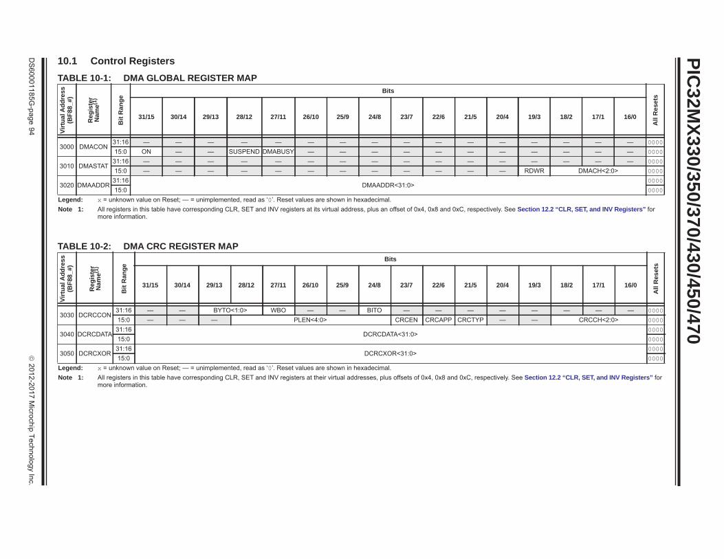
PIC32M
X330/350/370/430/450/470
DS
60001185G-page
94
2012-2017 M
icrochip Technology Inc.
10.1 Control RegistersTABLE 10-1: DMA GLOBAL REGISTER MAP
Virt
ual A
ddre
ss(B
F88_
#)
Reg
iste
rN
ame(1
)
Bit
Ran
ge
Bits
All
Res
ets
31/15 30/14 29/13 28/12 27/11 26/10 25/9 24/8 23/7 22/6 21/5 20/4 19/3 18/2 17/1 16/0
3000 DMACON31:16 — — — — — — — — — — — — — — — — 000015:0 ON — — SUSPEND DMABUSY — — — — — — — — — — — 0000
3010 DMASTAT31:16 — — — — — — — — — — — — — — — — 000015:0 — — — — — — — — — — — — RDWR DMACH<2:0> 0000
3020 DMAADDR31:16
DMAADDR<31:0>0000
15:0 0000Legend: x = unknown value on Reset; — = unimplemented, read as ‘0’. Reset values are shown in hexadecimal.Note 1: All registers in this table have corresponding CLR, SET and INV registers at its virtual address, plus an offset of 0x4, 0x8 and 0xC, respectively. See Section 12.2 “CLR, SET, and INV Registers” for
more information.
TABLE 10-2: DMA CRC REGISTER MAP
Virt
ual A
ddre
ss(B
F88_
#)
Reg
iste
rN
ame(1
)
Bit
Ran
ge
Bits
All
Res
ets
31/15 30/14 29/13 28/12 27/11 26/10 25/9 24/8 23/7 22/6 21/5 20/4 19/3 18/2 17/1 16/0
3030 DCRCCON31:16 — — BYTO<1:0> WBO — — BITO — — — — — — — — 000015:0 — — — PLEN<4:0> CRCEN CRCAPP CRCTYP — — CRCCH<2:0> 0000
3040 DCRCDATA31:16
DCRCDATA<31:0>0000
15:0 0000
3050 DCRCXOR31:16
DCRCXOR<31:0>0000
15:0 0000Legend: x = unknown value on Reset; — = unimplemented, read as ‘0’. Reset values are shown in hexadecimal.Note 1: All registers in this table have corresponding CLR, SET and INV registers at their virtual addresses, plus offsets of 0x4, 0x8 and 0xC, respectively. See Section 12.2 “CLR, SET, and INV Registers” for
more information.

2012-2017 M
icrochip Technology Inc.D
S60001185G
-page
95
PIC32M
X330/350/370/430/450/470
TABLE 10-3: DMA CHANNEL 0 THROUGH CHANNEL 3 REGISTER MAP Vi
rtua
l Add
ress
(BF8
8_#)
Reg
iste
rN
ame(1
)
Bit
Ran
ge
Bits
All
Res
ets
31/15 30/14 29/13 28/12 27/11 26/10 25/9 24/8 23/7 22/6 21/5 20/4 19/3 18/2 17/1 16/0
3060 DCH0CON31:16 — — — — — — — — — — — — — — — — 000015:0 CHBUSY — — — — — — CHCHNS CHEN CHAED CHCHN CHAEN — CHEDET CHPRI<1:0> 0000
3070 DCH0ECON31:16 — — — — — — — — CHAIRQ<7:0> 00FF15:0 CHSIRQ<7:0> CFORCE CABORT PATEN SIRQEN AIRQEN — — — FFF8
3080 DCH0INT31:16 — — — — — — — — CHSDIE CHSHIE CHDDIE CHDHIE CHBCIE CHCCIE CHTAIE CHERIE 000015:0 — — — — — — — — CHSDIF CHSHIF CHDDIF CHDHIF CHBCIF CHCCIF CHTAIF CHERIF 0000
3090 DCH0SSA31:16
CHSSA<31:0>0000
15:0 0000
30A0 DCH0DSA31:16
CHDSA<31:0>0000
15:0 0000
30B0 DCH0SSIZ31:16 — — — — — — — — — — — — — — — — 000015:0 CHSSIZ<15:0> 0000
30C0 DCH0DSIZ31:16 — — — — — — — — — — — — — — — — 000015:0 CHDSIZ<15:0> 0000
30D0 DCH0SPTR31:16 — — — — — — — — — — — — — — — — 000015:0 CHSPTR<15:0> 0000
30E0 DCH0DPTR31:16 — — — — — — — — — — — — — — — — 000015:0 CHDPTR<15:0> 0000
30F0 DCH0CSIZ31:16 — — — — — — — — — — — — — — — — 000015:0 CHCSIZ<15:0> 0000
3100 DCH0CPTR31:16 — — — — — — — — — — — — — — — — 000015:0 CHCPTR<15:0> 0000
3110 DCH0DAT31:16 — — — — — — — — — — — — — — — — 000015:0 — — — — — — — — CHPDAT<7:0> 0000
3120 DCH1CON31:16 — — — — — — — — — — — — — — — — 000015:0 CHBUSY — — — — — — CHCHNS CHEN CHAED CHCHN CHAEN — CHEDET CHPRI<1:0> 0000
3130 DCH1ECON31:16 — — — — — — — — CHAIRQ<7:0> 00FF15:0 CHSIRQ<7:0> CFORCE CABORT PATEN SIRQEN AIRQEN — — — FFF8
3140 DCH1INT31:16 — — — — — — — — CHSDIE CHSHIE CHDDIE CHDHIE CHBCIE CHCCIE CHTAIE CHERIE 000015:0 — — — — — — — — CHSDIF CHSHIF CHDDIF CHDHIF CHBCIF CHCCIF CHTAIF CHERIF 0000
3150 DCH1SSA31:16
CHSSA<31:0>0000
15:0 0000
3160 DCH1DSA31:16
CHDSA<31:0>0000
15:0 0000Legend: x = unknown value on Reset; — = unimplemented, read as ‘0’. Reset values are shown in hexadecimal.Note 1: All registers in this table have corresponding CLR, SET and INV registers at their virtual addresses, plus offsets of 0x4, 0x8 and 0xC, respectively. See Section 12.2 “CLR, SET, and INV Registers” for
more information.
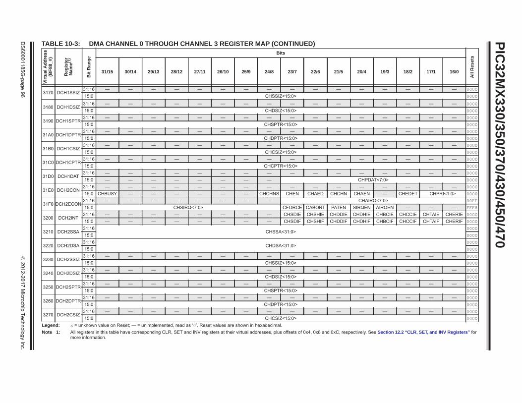
PIC32M
X330/350/370/430/450/470
DS
60001185G-page
96
2012-2017 M
icrochip Technology Inc.
3170 DCH1SSIZ31:16 — — — — — — — — — — — — — — — — 000015:0 CHSSIZ<15:0> 0000
3180 DCH1DSIZ31:16 — — — — — — — — — — — — — — — — 000015:0 CHDSIZ<15:0> 0000
3190 DCH1SPTR31:16 — — — — — — — — — — — — — — — — 000015:0 CHSPTR<15:0> 0000
31A0 DCH1DPTR31:16 — — — — — — — — — — — — — — — — 000015:0 CHDPTR<15:0> 0000
31B0 DCH1CSIZ31:16 — — — — — — — — — — — — — — — — 000015:0 CHCSIZ<15:0> 0000
31C0 DCH1CPTR31:16 — — — — — — — — — — — — — — — — 000015:0 CHCPTR<15:0> 0000
31D0 DCH1DAT31:16 — — — — — — — — — — — — — — — — 000015:0 — — — — — — — — CHPDAT<7:0> 0000
31E0 DCH2CON31:16 — — — — — — — — — — — — — — — — 000015:0 CHBUSY — — — — — — CHCHNS CHEN CHAED CHCHN CHAEN — CHEDET CHPRI<1:0> 0000
31F0 DCH2ECON31:16 — — — — — — — — CHAIRQ<7:0> 00FF15:0 CHSIRQ<7:0> CFORCE CABORT PATEN SIRQEN AIRQEN — — — FFF8
3200 DCH2INT31:16 — — — — — — — — CHSDIE CHSHIE CHDDIE CHDHIE CHBCIE CHCCIE CHTAIE CHERIE 000015:0 — — — — — — — — CHSDIF CHSHIF CHDDIF CHDHIF CHBCIF CHCCIF CHTAIF CHERIF 0000
3210 DCH2SSA31:16
CHSSA<31:0>0000
15:0 0000
3220 DCH2DSA31:16
CHDSA<31:0>0000
15:0 0000
3230 DCH2SSIZ31:16 — — — — — — — — — — — — — — — — 000015:0 CHSSIZ<15:0> 0000
3240 DCH2DSIZ31:16 — — — — — — — — — — — — — — — — 000015:0 CHDSIZ<15:0> 0000
3250 DCH2SPTR31:16 — — — — — — — — — — — — — — — — 000015:0 CHSPTR<15:0> 0000
3260 DCH2DPTR31:16 — — — — — — — — — — — — — — — — 000015:0 CHDPTR<15:0> 0000
3270 DCH2CSIZ31:16 — — — — — — — — — — — — — — — — 000015:0 CHCSIZ<15:0> 0000
TABLE 10-3: DMA CHANNEL 0 THROUGH CHANNEL 3 REGISTER MAP (CONTINUED)Vi
rtua
l Add
ress
(BF8
8_#)
Reg
iste
rN
ame(1
)
Bit
Ran
ge
Bits
All
Res
ets
31/15 30/14 29/13 28/12 27/11 26/10 25/9 24/8 23/7 22/6 21/5 20/4 19/3 18/2 17/1 16/0
Legend: x = unknown value on Reset; — = unimplemented, read as ‘0’. Reset values are shown in hexadecimal.Note 1: All registers in this table have corresponding CLR, SET and INV registers at their virtual addresses, plus offsets of 0x4, 0x8 and 0xC, respectively. See Section 12.2 “CLR, SET, and INV Registers” for
more information.

2012-2017 M
icrochip Technology Inc.D
S60001185G
-page
97
PIC32M
X330/350/370/430/450/470
3280 DCH2CPTR31:16 — — — — — — — — — — — — — — — — 0000
15:0 CHCPTR<15:0> 0000
3290 DCH2DAT31:16 — — — — — — — — — — — — — — — — 0000
15:0 — — — — — — — — CHPDAT<7:0> 0000
32A0 DCH3CON31:16 — — — — — — — — — — — — — — — — 000015:0 CHBUSY — — — — — — CHCHNS CHEN CHAED CHCHN CHAEN — CHEDET CHPRI<1:0> 0000
32B0 DCH3ECON31:16 — — — — — — — — CHAIRQ<7:0> 00FF15:0 CHSIRQ<7:0> CFORCE CABORT PATEN SIRQEN AIRQEN — — — FFF8
32C0 DCH3INT31:16 — — — — — — — — CHSDIE CHSHIE CHDDIE CHDHIE CHBCIE CHCCIE CHTAIE CHERIE 0000
15:0 — — — — — — — — CHSDIF CHSHIF CHDDIF CHDHIF CHBCIF CHCCIF CHTAIF CHERIF 0000
32D0 DCH3SSA31:16
CHSSA<31:0>0000
15:0 0000
32E0 DCH3DSA31:16
CHDSA<31:0>0000
15:0 0000
32F0 DCH3SSIZ31:16 — — — — — — — — — — — — — — — — 000015:0 CHSSIZ<15:0> 0000
3300 DCH3DSIZ31:16 — — — — — — — — — — — — — — — — 000015:0 CHDSIZ<15:0> 0000
3310 DCH3SPTR31:16 — — — — — — — — — — — — — — — — 000015:0 CHSPTR<15:0> 0000
3320 DCH3DPTR31:16 — — — — — — — — — — — — — — — — 000015:0 CHDPTR<15:0> 0000
3330 DCH3CSIZ31:16 — — — — — — — — — — — — — — — — 000015:0 CHCSIZ<15:0> 0000
3340 DCH3CPTR31:16 — — — — — — — — — — — — — — — — 000015:0 CHCPTR<15:0> 0000
3350 DCH3DAT31:16 — — — — — — — — — — — — — — — — 000015:0 — — — — — — — — CHPDAT<7:0> 0000
TABLE 10-3: DMA CHANNEL 0 THROUGH CHANNEL 3 REGISTER MAP (CONTINUED)Vi
rtua
l Add
ress
(BF8
8_#)
Reg
iste
rN
ame(1
)
Bit
Ran
ge
Bits
All
Res
ets
31/15 30/14 29/13 28/12 27/11 26/10 25/9 24/8 23/7 22/6 21/5 20/4 19/3 18/2 17/1 16/0
Legend: x = unknown value on Reset; — = unimplemented, read as ‘0’. Reset values are shown in hexadecimal.Note 1: All registers in this table have corresponding CLR, SET and INV registers at their virtual addresses, plus offsets of 0x4, 0x8 and 0xC, respectively. See Section 12.2 “CLR, SET, and INV Registers” for
more information.
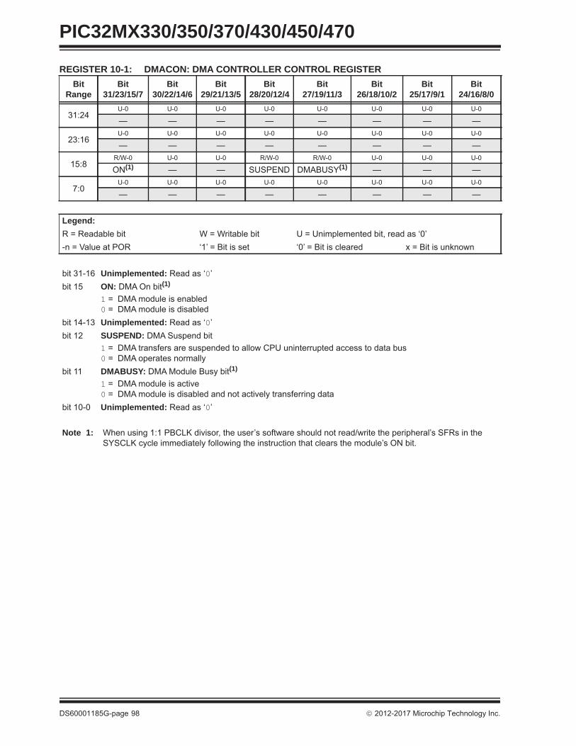
PIC32MX330/350/370/430/450/470
DS60001185G-page 98 2012-2017 Microchip Technology Inc.
REGISTER 10-1: DMACON: DMA CONTROLLER CONTROL REGISTER Bit
RangeBit
31/23/15/7Bit
30/22/14/6Bit
29/21/13/5Bit
28/20/12/4Bit
27/19/11/3Bit
26/18/10/2Bit
25/17/9/1Bit
24/16/8/0
31:24U-0 U-0 U-0 U-0 U-0 U-0 U-0 U-0
— — — — — — — —
23:16U-0 U-0 U-0 U-0 U-0 U-0 U-0 U-0
— — — — — — — —
15:8R/W-0 U-0 U-0 R/W-0 R/W-0 U-0 U-0 U-0
ON(1) — — SUSPEND DMABUSY(1) — — —
7:0U-0 U-0 U-0 U-0 U-0 U-0 U-0 U-0
— — — — — — — —
Legend:R = Readable bit W = Writable bit U = Unimplemented bit, read as ‘0’-n = Value at POR ‘1’ = Bit is set ‘0’ = Bit is cleared x = Bit is unknown
bit 31-16 Unimplemented: Read as ‘0’bit 15 ON: DMA On bit(1)
1 = DMA module is enabled0 = DMA module is disabled
bit 14-13 Unimplemented: Read as ‘0’bit 12 SUSPEND: DMA Suspend bit
1 = DMA transfers are suspended to allow CPU uninterrupted access to data bus0 = DMA operates normally
bit 11 DMABUSY: DMA Module Busy bit(1)
1 = DMA module is active0 = DMA module is disabled and not actively transferring data
bit 10-0 Unimplemented: Read as ‘0’
Note 1: When using 1:1 PBCLK divisor, the user’s software should not read/write the peripheral’s SFRs in the SYSCLK cycle immediately following the instruction that clears the module’s ON bit.

REGISTER 10-3: DMAADDR: DMA ADDRESS REGISTERBit
RangeBit
31/23/15/7Bit
30/22/14/6Bit
29/21/13/5Bit
28/20/12/4Bit
27/19/11/3Bit
26/18/10/2Bit
25/17/9/1Bit
24/16/8/0
31:24R-0 R-0 R-0 R-0 R-0 R-0 R-0 R-0
DMAADDR<31:24>
23:16R-0 R-0 R-0 R-0 R-0 R-0 R-0 R-0
DMAADDR<23:16>
15:8R-0 R-0 R-0 R-0 R-0 R-0 R-0 R-0
DMAADDR<15:8>
7:0R-0 R-0 R-0 R-0 R-0 R-0 R-0 R-0
DMAADDR<7:0>
Legend:R = Readable bit W = Writable bit U = Unimplemented bit, read as ‘0’-n = Value at POR ‘1’ = Bit is set ‘0’ = Bit is cleared x = Bit is unknown
bit 31-0 DMAADDR<31:0>: DMA Module Address bitsThese bits contain the address of the most recent DMA access.
2012-2017 Microchip Technology Inc. DS60001185G-page 99
PIC32MX330/350/370/430/450/470
REGISTER 10-2: DMASTAT: DMA STATUS REGISTERBit
RangeBit
31/23/15/7Bit
30/22/14/6Bit
29/21/13/5Bit
28/20/12/4Bit
27/19/11/3Bit
26/18/10/2Bit
25/17/9/1Bit
24/16/8/0
31:24U-0 U-0 U-0 U-0 U-0 U-0 U-0 U-0
— — — — — — — —
23:16U-0 U-0 U-0 U-0 U-0 U-0 U-0 U-0
— — — — — — — —
15:8U-0 U-0 U-0 U-0 U-0 U-0 U-0 U-0
— — — — — — — —
7:0U-0 U-0 U-0 U-0 R-0 R-0 R-0 R-0
— — — — RDWR DMACH<2:0>
Legend:R = Readable bit W = Writable bit U = Unimplemented bit, read as ‘0’-n = Value at POR ‘1’ = Bit is set ‘0’ = Bit is cleared x = Bit is unknown
bit 31-4 Unimplemented: Read as ‘0’bit 3 RDWR: Read/Write Status bit
1 = Last DMA bus access was a read0 = Last DMA bus access was a write
bit 2-0 DMACH<2:0>: DMA Channel bitsThese bits contain the value of the most recent active DMA channel.

PIC32MX330/350/370/430/450/470
DS60001185G-page 100 2012-2017 Microchip Technology Inc.
REGISTER 10-4: DCRCCON: DMA CRC CONTROL REGISTER Bit
RangeBit
31/23/15/7Bit
30/22/14/6Bit
29/21/13/5Bit
28/20/12/4Bit
27/19/11/3Bit
26/18/10/2Bit
25/17/9/1Bit
24/16/8/0
31:24U-0 U-0 R/W-0 R/W-0 R/W-0 U-0 U-0 R/W-0
— — BYTO<1:0> WBO(1) — — BITO(1)
23:16U-0 U-0 U-0 U-0 U-0 U-0 U-0 U-0
— — — — — — — —
15:8U-0 U-0 U-0 R/W-0 R/W-0 R/W-0 R/W-0 R/W-0
— — — PLEN<4:0>
7:0R/W-0 R/W-0 R/W-0 U-0 U-0 R/W-0 R/W-0 R/W-0
CRCEN CRCAPP(1) CRCTYP — — CRCCH<2:0>
Legend:R = Readable bit W = Writable bit U = Unimplemented bit, read as ‘0’-n = Value at POR ‘1’ = Bit is set ‘0’ = Bit is cleared x = Bit is unknown
bit 31-30 Unimplemented: Read as ‘0’bit 29-28 BYTO<1:0>: CRC Byte Order Selection bits
11 = Endian byte swap on half-word boundaries (i.e., source half-word order with reverse source byte order per half-word)
10 = Swap half-words on word boundaries (i.e., reverse source half-word order with source byte order per half-word)
01 = Endian byte swap on word boundaries (i.e., reverse source byte order)00 = No swapping (i.e., source byte order)
bit 27 WBO: CRC Write Byte Order Selection bit(1)
1 = Source data is written to the destination re-ordered as defined by BYTO<1:0>0 = Source data is written to the destination unaltered
bit 26-25 Unimplemented: Read as ‘0’bit 24 BITO: CRC Bit Order Selection bit(1)
When CRCTYP (DCRCCON<15>) = 1 (CRC module is in IP Header mode):1 = The IP header checksum is calculated Least Significant bit (LSb) first (i.e., reflected)0 = The IP header checksum is calculated Most Significant bit (MSb) first (i.e., not reflected)
When CRCTYP (DCRCCON<15>) = 0 (CRC module is in LFSR mode):1 = The LFSR CRC is calculated Least Significant bit first (i.e., reflected)0 = The LFSR CRC is calculated Most Significant bit first (i.e., not reflected)
bit 23-13 Unimplemented: Read as ‘0’bit 12-8 PLEN<4:0>: Polynomial Length bits(1)
When CRCTYP (DCRCCON<15>) = 1 (CRC module is in IP Header mode):These bits are unused.
When CRCTYP (DCRCCON<15>) = 0 (CRC module is in LFSR mode):Denotes the length of the polynomial – 1.
bit 7 CRCEN: CRC Enable bit1 = CRC module is enabled and channel transfers are routed through the CRC module0 = CRC module is disabled and channel transfers proceed normally
Note 1: When WBO = 1, unaligned transfers are not supported and the CRCAPP bit cannot be set.

2012-2017 Microchip Technology Inc. DS60001185G-page 101
PIC32MX330/350/370/430/450/470
bit 6 CRCAPP: CRC Append Mode bit(1)
1 = The DMA transfers data from the source into the CRC but NOT to the destination. When a block transfer completes the DMA writes the calculated CRC value to the location given by CHxDSA
0 = The DMA transfers data from the source through the CRC obeying WBO as it writes the data to the destination
bit 5 CRCTYP: CRC Type Selection bit1 = The CRC module will calculate an IP header checksum0 = The CRC module will calculate a LFSR CRC
bit 4-3 Unimplemented: Read as ‘0’bit 2-0 CRCCH<2:0>: CRC Channel Select bits
111 = CRC is assigned to Channel 7110 = CRC is assigned to Channel 6101 = CRC is assigned to Channel 5100 = CRC is assigned to Channel 4011 = CRC is assigned to Channel 3010 = CRC is assigned to Channel 2001 = CRC is assigned to Channel 1000 = CRC is assigned to Channel 0
REGISTER 10-4: DCRCCON: DMA CRC CONTROL REGISTER (CONTINUED)
Note 1: When WBO = 1, unaligned transfers are not supported and the CRCAPP bit cannot be set.

REGISTER 10-6: DCRCXOR: DMA CRCXOR ENABLE REGISTERBit
RangeBit
31/23/15/7Bit
30/22/14/6Bit
29/21/13/5Bit
28/20/12/4Bit
27/19/11/3Bit
26/18/10/2Bit
25/17/9/1Bit
24/16/8/0
31:24R/W-0 R/W-0 R/W-0 R/W-0 R/W-0 R/W-0 R/W-0 R/W-0
DCRCXOR<31:24>
23:16R/W-0 R/W-0 R/W-0 R/W-0 R/W-0 R/W-0 R/W-0 R/W-0
DCRCXOR<23:16>
15:8R/W-0 R/W-0 R/W-0 R/W-0 R/W-0 R/W-0 R/W-0 R/W-0
DCRCXOR<15:8>
7:0R/W-0 R/W-0 R/W-0 R/W-0 R/W-0 R/W-0 R/W-0 R/W-0
DCRCXOR<7:0>
Legend:R = Readable bit W = Writable bit U = Unimplemented bit, read as ‘0’-n = Value at POR ‘1’ = Bit is set ‘0’ = Bit is cleared x = Bit is unknown
bit 31-0 DCRCXOR<31:0>: CRC XOR Register bitsWhen CRCTYP (DCRCCON<15>) = 1 (CRC module is in IP Header mode):This register is unused.
When CRCTYP (DCRCCON<15>) = 0 (CRC module is in LFSR mode):1 = Enable the XOR input to the Shift register0 = Disable the XOR input to the Shift register; data is shifted in directly from the previous stage in
the register
PIC32MX330/350/370/430/450/470
DS60001185G-page 102 2012-2017 Microchip Technology Inc.
REGISTER 10-5: DCRCDATA: DMA CRC DATA REGISTERBit
RangeBit
31/23/15/7Bit
30/22/14/6Bit
29/21/13/5Bit
28/20/12/4Bit
27/19/11/3Bit
26/18/10/2Bit
25/17/9/1Bit
24/16/8/0
31:24R/W-0 R/W-0 R/W-0 R/W-0 R/W-0 R/W-0 R/W-0 R/W-0
DCRCDATA<31:24>
23:16R/W-0 R/W-0 R/W-0 R/W-0 R/W-0 R/W-0 R/W-0 R/W-0
DCRCDATA<23:16>
15:8R/W-0 R/W-0 R/W-0 R/W-0 R/W-0 R/W-0 R/W-0 R/W-0
DCRCDATA<15:8>
7:0R/W-0 R/W-0 R/W-0 R/W-0 R/W-0 R/W-0 R/W-0 R/W-0
DCRCDATA<7:0>
Legend:R = Readable bit W = Writable bit U = Unimplemented bit, read as ‘0’-n = Value at POR ‘1’ = Bit is set ‘0’ = Bit is cleared x = Bit is unknown
bit 31-0 DCRCDATA<31:0>: CRC Data Register bitsWriting to this register will seed the CRC generator. Reading from this register will return the current value of the CRC. Bits greater than PLEN will return ‘0’ on any read.
When CRCTYP (DCRCCON<15>) = 1 (CRC module is in IP Header mode):Only the lower 16 bits contain IP header checksum information. The upper 16 bits are always ‘0’. Data written to this register is converted and read back in 1’s complement form (i.e., current IP header checksum value).
When CRCTYP (DCRCCON<15>) = 0 (CRC module is in LFSR mode):Bits greater than PLEN will return ‘0’ on any read.

2012-2017 Microchip Technology Inc. DS60001185G-page 103
PIC32MX330/350/370/430/450/470
REGISTER 10-7: DCHxCON: DMA CHANNEL ‘x’ CONTROL REGISTER Bit
RangeBit
31/23/15/7Bit
30/22/14/6Bit
29/21/13/5Bit
28/20/12/4Bit
27/19/11/3Bit
26/18/10/2Bit
25/17/9/1Bit
24/16/8/0
31:24U-0 U-0 U-0 U-0 U-0 U-0 U-0 U-0
— — — — — — — —
23:16U-0 U-0 U-0 U-0 U-0 U-0 U-0 U-0
— — — — — — — —
15:8R/W-0 U-0 U-0 U-0 U-0 U-0 U-0 R/W-0
CHBUSY — — — — — — CHCHNS(1)
7:0R/W-0 R/W-0 R/W-0 R/W-0 U-0 R-0 R/W-0 R/W-0
CHEN(2) CHAED CHCHN CHAEN — CHEDET CHPRI<1:0>
Legend:R = Readable bit W = Writable bit U = Unimplemented bit, read as ‘0’-n = Value at POR ‘1’ = Bit is set ‘0’ = Bit is cleared x = Bit is unknown
bit 31-16 Unimplemented: Read as ‘0’bit 15 CHBUSY: Channel Busy bit
1 = Channel is active or has been enabled0 = Channel is inactive or has been disabled
bit 14-9 Unimplemented: Read as ‘0’bit 8 CHCHNS: Chain Channel Selection bit(1)
1 = Chain to channel lower in natural priority (CH1 will be enabled by CH2 transfer complete)0 = Chain to channel higher in natural priority (CH1 will be enabled by CH0 transfer complete)
bit 7 CHEN: Channel Enable bit(2)
1 = Channel is enabled0 = Channel is disabled
bit 6 CHAED: Channel Allow Events If Disabled bit1 = Channel start/abort events will be registered, even if the channel is disabled0 = Channel start/abort events will be ignored if the channel is disabled
bit CHCHN: Channel Chain Enable bit1 = Allow channel to be chained0 = Do not allow channel to be chained
bit 4 CHAEN: Channel Automatic Enable bit1 = Channel is continuously enabled, and not automatically disabled after a block transfer is complete0 = Channel is disabled on block transfer complete
bit 3 Unimplemented: Read as ‘0’bit 2 CHEDET: Channel Event Detected bit
1 = An event has been detected0 = No events have been detected
bit 1-0 CHPRI<1:0>: Channel Priority bits11 = Channel has priority 3 (highest)10 = Channel has priority 201 = Channel has priority 100 = Channel has priority 0
Note 1: The chain selection bit takes effect when chaining is enabled (i.e., CHCHN = 1).2: When the channel is suspended by clearing this bit, the user application should poll the CHBUSY bit (if
available on the device variant) to see when the channel is suspended, as it may take some clock cycles to complete a current transaction before the channel is suspended.

PIC32MX330/350/370/430/450/470
DS60001185G-page 104 2012-2017 Microchip Technology Inc.
REGISTER 10-8: DCHxECON: DMA CHANNEL ‘x’ EVENT CONTROL REGISTER Bit
RangeBit
31/23/15/7Bit
30/22/14/6Bit
29/21/13/5Bit
28/20/12/4Bit
27/19/11/3Bit
26/18/10/2Bit
25/17/9/1Bit
24/16/8/0
31:24U-0 U-0 U-0 U-0 U-0 U-0 U-0 U-0
— — — — — — — —
23:16R/W-1 R/W-1 R/W-1 R/W-1 R/W-1 R/W-1 R/W-1 R/W-1
CHAIRQ<7:0>(1)
15:8R/W-1 R/W-1 R/W-1 R/W-1 R/W-1 R/W-1 R/W-1 R/W-1
CHSIRQ<7:0>(1)
7:0S-0 S-0 R/W-0 R/W-0 R/W-0 U-0 U-0 U-0
CFORCE CABORT PATEN SIRQEN AIRQEN — — —
Legend: S = Settable bitR = Readable bit W = Writable bit U = Unimplemented bit, read as ‘0’-n = Value at POR ‘1’ = Bit is set ‘0’ = Bit is cleared x = Bit is unknown
bit 31-24 Unimplemented: Read as ‘0’bit 23-16 CHAIRQ<7:0>: Channel Transfer Abort IRQ bits(1)
11111111 = Interrupt 255 will abort any transfers in progress and set CHAIF flag•••00000001 = Interrupt 1 will abort any transfers in progress and set CHAIF flag00000000 = Interrupt 0 will abort any transfers in progress and set CHAIF flag
bit 15-8 CHSIRQ<7:0>: Channel Transfer Start IRQ bits(1)
11111111 = Interrupt 255 will initiate a DMA transfer•••00000001 = Interrupt 1 will initiate a DMA transfer00000000 = Interrupt 0 will initiate a DMA transfer
bit 7 CFORCE: DMA Forced Transfer bit1 = A DMA transfer is forced to begin when this bit is written to a ‘1’0 = This bit always reads ‘0’
bit 6 CABORT: DMA Abort Transfer bit1 = A DMA transfer is aborted when this bit is written to a ‘1’0 = This bit always reads ‘0’
bit 5 PATEN: Channel Pattern Match Abort Enable bit1 = Abort transfer and clear CHEN on pattern match0 = Pattern match is disabled
bit 4 SIRQEN: Channel Start IRQ Enable bit1 = Start channel cell transfer if an interrupt matching CHSIRQ occurs0 = Interrupt number CHSIRQ is ignored and does not start a transfer
bit 3 AIRQEN: Channel Abort IRQ Enable bit1 = Channel transfer is aborted if an interrupt matching CHAIRQ occurs0 = Interrupt number CHAIRQ is ignored and does not terminate a transfer
bit 2-0 Unimplemented: Read as ‘0’
Note 1: See Table 7-1: “Interrupt IRQ, Vector and Bit Location” for the list of available interrupt IRQ sources.

2012-2017 Microchip Technology Inc. DS60001185G-page 105
PIC32MX330/350/370/430/450/470
REGISTER 10-9: DCHxINT: DMA CHANNEL ‘x’ INTERRUPT CONTROL REGISTER Bit
RangeBit
31/23/15/7Bit
30/22/14/6Bit
29/21/13/5Bit
28/20/12/4Bit
27/19/11/3Bit
26/18/10/2Bit
25/17/9/1Bit
24/16/8/0
31:24U-0 U-0 U-0 U-0 U-0 U-0 U-0 U-0
— — — — — — — —
23:16R/W-0 R/W-0 R/W-0 R/W-0 R/W-0 R/W-0 R/W-0 R/W-0
CHSDIE CHSHIE CHDDIE CHDHIE CHBCIE CHCCIE CHTAIE CHERIE
15:8U-0 U-0 U-0 U-0 U-0 U-0 U-0 U-0
— — — — — — — —
7:0R/W-0 R/W-0 R/W-0 R/W-0 R/W-0 R/W-0 R/W-0 R/W-0
CHSDIF CHSHIF CHDDIF CHDHIF CHBCIF CHCCIF CHTAIF CHERIF
Legend:R = Readable bit W = Writable bit U = Unimplemented bit, read as ‘0’-n = Value at POR ‘1’ = Bit is set ‘0’ = Bit is cleared x = Bit is unknown
bit 31-24 Unimplemented: Read as ‘0’bit 23 CHSDIE: Channel Source Done Interrupt Enable bit
1 = Interrupt is enabled0 = Interrupt is disabled
bit 22 CHSHIE: Channel Source Half Empty Interrupt Enable bit1 = Interrupt is enabled0 = Interrupt is disabled
bit 21 CHDDIE: Channel Destination Done Interrupt Enable bit1 = Interrupt is enabled0 = Interrupt is disabled
bit 20 CHDHIE: Channel Destination Half Full Interrupt Enable bit1 = Interrupt is enabled0 = Interrupt is disabled
bit 19 CHBCIE: Channel Block Transfer Complete Interrupt Enable bit1 = Interrupt is enabled0 = Interrupt is disabled
bit 18 CHCCIE: Channel Cell Transfer Complete Interrupt Enable bit1 = Interrupt is enabled0 = Interrupt is disabled
bit 17 CHTAIE: Channel Transfer Abort Interrupt Enable bit1 = Interrupt is enabled0 = Interrupt is disabled
bit 16 CHERIE: Channel Address Error Interrupt Enable bit1 = Interrupt is enabled0 = Interrupt is disabled
bit 15-8 Unimplemented: Read as ‘0’bit 7 CHSDIF: Channel Source Done Interrupt Flag bit
1 = Channel Source Pointer has reached end of source (CHSPTR = CHSSIZ)0 = No interrupt is pending
bit 6 CHSHIF: Channel Source Half Empty Interrupt Flag bit1 = Channel Source Pointer has reached midpoint of source (CHSPTR = CHSSIZ/2) 0 = No interrupt is pending
bit 5 CHDDIF: Channel Destination Done Interrupt Flag bit1 = Channel Destination Pointer has reached end of destination (CHDPTR = CHDSIZ) 0 = No interrupt is pending

PIC32MX330/350/370/430/450/470
DS60001185G-page 106 2012-2017 Microchip Technology Inc.
bit 4 CHDHIF: Channel Destination Half Full Interrupt Flag bit1 = Channel Destination Pointer has reached midpoint of destination (CHDPTR = CHDSIZ/2) 0 = No interrupt is pending
bit 3 CHBCIF: Channel Block Transfer Complete Interrupt Flag bit1 = A block transfer has been completed (the larger of CHSSIZ/CHDSIZ bytes has been transferred), or a
pattern match event occurs 0 = No interrupt is pending
bit 2 CHCCIF: Channel Cell Transfer Complete Interrupt Flag bit1 = A cell transfer has been completed (CHCSIZ bytes have been transferred) 0 = No interrupt is pending
bit 1 CHTAIF: Channel Transfer Abort Interrupt Flag bit1 = An interrupt matching CHAIRQ has been detected and the DMA transfer has been aborted 0 = No interrupt is pending
bit 0 CHERIF: Channel Address Error Interrupt Flag bit1 = A channel address error has been detected
Either the source or the destination address is invalid.0 = No interrupt is pending
REGISTER 10-9: DCHxINT: DMA CHANNEL ‘x’ INTERRUPT CONTROL REGISTER (CONTINUED)
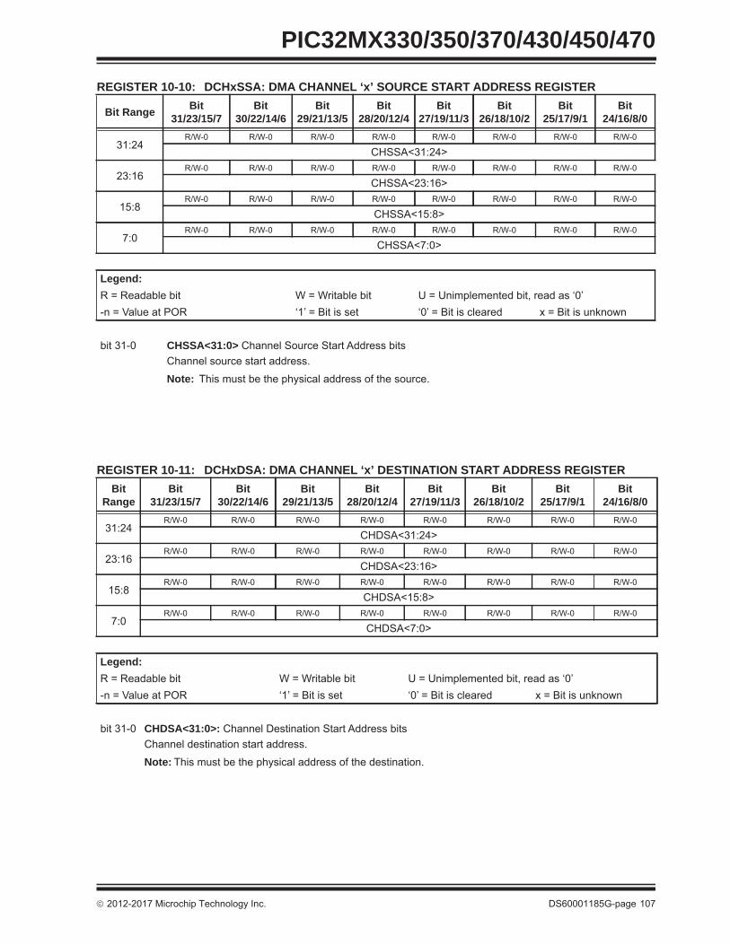
REGISTER 10-11: DCHxDSA: DMA CHANNEL ‘x’ DESTINATION START ADDRESS REGISTERBit
RangeBit
31/23/15/7Bit
30/22/14/6Bit
29/21/13/5Bit
28/20/12/4Bit
27/19/11/3Bit
26/18/10/2Bit
25/17/9/1Bit
24/16/8/0
31:24R/W-0 R/W-0 R/W-0 R/W-0 R/W-0 R/W-0 R/W-0 R/W-0
CHDSA<31:24>
23:16R/W-0 R/W-0 R/W-0 R/W-0 R/W-0 R/W-0 R/W-0 R/W-0
CHDSA<23:16>
15:8R/W-0 R/W-0 R/W-0 R/W-0 R/W-0 R/W-0 R/W-0 R/W-0
CHDSA<15:8>
7:0R/W-0 R/W-0 R/W-0 R/W-0 R/W-0 R/W-0 R/W-0 R/W-0
CHDSA<7:0>
Legend:R = Readable bit W = Writable bit U = Unimplemented bit, read as ‘0’-n = Value at POR ‘1’ = Bit is set ‘0’ = Bit is cleared x = Bit is unknown
CHDSA<31:0>: Channel Destination Start Address bitsChannel destination start address.
Note: This must be the physical address of the destination.
2012-2017 Microchip Technology Inc. DS60001185G-page 107
PIC32MX330/350/370/430/450/470
REGISTER 10-10: DCHxSSA: DMA CHANNEL ‘x’ SOURCE START ADDRESS REGISTER
Bit Range Bit31/23/15/7
Bit30/22/14/6
Bit29/21/13/5
Bit28/20/12/4
Bit27/19/11/3
Bit26/18/10/2
Bit25/17/9/1
Bit24/16/8/0
31:24R/W-0 R/W-0 R/W-0 R/W-0 R/W-0 R/W-0 R/W-0 R/W-0
CHSSA<31:24>
23:16R/W-0 R/W-0 R/W-0 R/W-0 R/W-0 R/W-0 R/W-0 R/W-0
CHSSA<23:16>
15:8R/W-0 R/W-0 R/W-0 R/W-0 R/W-0 R/W-0 R/W-0 R/W-0
CHSSA<15:8>
7:0R/W-0 R/W-0 R/W-0 R/W-0 R/W-0 R/W-0 R/W-0 R/W-0
CHSSA<7:0>
Legend:R = Readable bit W = Writable bit U = Unimplemented bit, read as ‘0’-n = Value at POR ‘1’ = Bit is set ‘0’ = Bit is cleared x = Bit is unknown
bit 31-0 CHSSA<31:0> Channel Source Start Address bitsChannel source start address.
Note: This must be the physical address of the source.
bit 31-0

REGISTER 10-13: DCHxDSIZ: DMA CHANNEL ‘x’ DESTINATION SIZE REGISTERBit
RangeBit
31/23/15/7Bit
30/22/14/6Bit
29/21/13/5Bit
28/20/12/4Bit
27/19/11/3Bit
26/18/10/2Bit
25/17/9/1Bit
24/16/8/0
31:24U-0 U-0 U-0 U-0 U-0 U-0 U-0 U-0
— — — — — — — —
23:16U-0 U-0 U-0 U-0 U-0 U-0 U-0 U-0
— — — — — — — —
15:8R/W-0 R/W-0 R/W-0 R/W-0 R/W-0 R/W-0 R/W-0 R/W-0
CHDSIZ<15:8>
7:0R/W-0 R/W-0 R/W-0 R/W-0 R/W-0 R/W-0 R/W-0 R/W-0
CHDSIZ<7:0>
Legend:R = Readable bit W = Writable bit U = Unimplemented bit, read as ‘0’-n = Value at POR ‘1’ = Bit is set ‘0’ = Bit is cleared x = Bit is unknown
Unimplemented: Read as ‘0’CHDSIZ<15:0>: Channel Destination Size bits
•••0000000000000010 = 2 byte destination size0000000000000001 = 1 byte destination size0000000000000000 = 65,536 byte destination size
PIC32MX330/350/370/430/450/470
DS60001185G-page 108 2012-2017 Microchip Technology Inc.
REGISTER 10-12: DCHxSSIZ: DMA CHANNEL ‘x’ SOURCE SIZE REGISTERBit
RangeBit
31/23/15/7Bit
30/22/14/6Bit
29/21/13/5Bit
28/20/12/4Bit
27/19/11/3Bit
26/18/10/2Bit
25/17/9/1Bit
24/16/8/0
31:24U-0 U-0 U-0 U-0 U-0 U-0 U-0 U-0
— — — — — — — —
23:16U-0 U-0 U-0 U-0 U-0 U-0 U-0 U-0
— — — — — — — —
15:8R/W-0 R/W-0 R/W-0 R/W-0 R/W-0 R/W-0 R/W-0 R/W-0
CHSSIZ<15:8>
7:0R/W-0 R/W-0 R/W-0 R/W-0 R/W-0 R/W-0 R/W-0 R/W-0
CHSSIZ<7:0>
Legend:R = Readable bit W = Writable bit U = Unimplemented bit, read as ‘0’-n = Value at POR ‘1’ = Bit is set ‘0’ = Bit is cleared x = Bit is unknown
bit 31-16 Unimplemented: Read as ‘0’bit 15-0 CHSSIZ<15:0>: Channel Source Size bits
1111111111111111 = 65,535 byte source size•••0000000000000010 = 2 byte source size0000000000000001 = 1 byte source size0000000000000000 = 65,536 byte source size
bit 31-16bit 15-0
1111111111111111 = 65,535 byte destination size

REGISTER 10-15: DCHxDPTR: DMA CHANNEL ‘x’ DESTINATION POINTER REGISTERBit
RangeBit
31/23/15/7Bit
30/22/14/6Bit
29/21/13/5Bit
28/20/12/4Bit
27/19/11/3Bit
26/18/10/2Bit
25/17/9/1Bit
24/16/8/0
31:24U-0 U-0 U-0 U-0 U-0 U-0 U-0 U-0
— — — — — — — —
23:16U-0 U-0 U-0 U-0 U-0 U-0 U-0 U-0
— — — — — — — —
15:8R-0 R-0 R-0 R-0 R-0 R-0 R-0 R-0
CHDPTR<15:8>
7:0R-0 R-0 R-0 R-0 R-0 R-0 R-0 R-0
CHDPTR<7:0>
Legend:R = Readable bit W = Writable bit U = Unimplemented bit, read as ‘0’-n = Value at POR ‘1’ = Bit is set ‘0’ = Bit is cleared x = Bit is unknown
Unimplemented: Read as ‘0’CHDPTR<15:0>: Channel Destination Pointer bits
•••0000000000000001 = Points to byte 1 of the destination0000000000000000 = Points to byte 0 of the destination
2012-2017 Microchip Technology Inc. DS60001185G-page 109
PIC32MX330/350/370/430/450/470
REGISTER 10-14: DCHxSPTR: DMA CHANNEL ‘x’ SOURCE POINTER REGISTERBit
RangeBit
31/23/15/7Bit
30/22/14/6Bit
29/21/13/5Bit
28/20/12/4Bit
27/19/11/3Bit
26/18/10/2Bit
25/17/9/1Bit
24/16/8/0
31:24U-0 U-0 U-0 U-0 U-0 U-0 U-0 U-0
— — — — — — — —
23:16U-0 U-0 U-0 U-0 U-0 U-0 U-0 U-0
— — — — — — — —
15:8R-0 R-0 R-0 R-0 R-0 R-0 R-0 R-0
CHSPTR<15:8>
7:0R-0 R-0 R-0 R-0 R-0 R-0 R-0 R-0
CHSPTR<7:0>
Legend:R = Readable bit W = Writable bit U = Unimplemented bit, read as ‘0’-n = Value at POR ‘1’ = Bit is set ‘0’ = Bit is cleared x = Bit is unknown
bit 31-16 Unimplemented: Read as ‘0’bit 15-0 CHSPTR<15:0>: Channel Source Pointer bits
1111111111111111 = Points to byte 65,535 of the source•••0000000000000001 = Points to byte 1 of the source0000000000000000 = Points to byte 0 of the source
Note: When in Pattern Detect mode, this register is reset on a pattern detect.
bit 31-16bit 15-0
1111111111111111 = Points to byte 65,535 of the destination

REGISTER 10-17: DCHxCPTR: DMA CHANNEL ‘x’ CELL POINTER REGISTERBit
RangeBit
31/23/15/7Bit
30/22/14/6Bit
29/21/13/5Bit
28/20/12/4Bit
27/19/11/3Bit
26/18/10/2Bit
25/17/9/1Bit
24/16/8/0
31:24U-0 U-0 U-0 U-0 U-0 U-0 U-0 U-0
— — — — — — — —
23:16U-0 U-0 U-0 U-0 U-0 U-0 U-0 U-0
— — — — — — — —
15:8R-0 R-0 R-0 R-0 R-0 R-0 R-0 R-0
CHCPTR<15:8>
7:0R-0 R-0 R-0 R-0 R-0 R-0 R-0 R-0
CHCPTR<7:0>
Legend:R = Readable bit W = Writable bit U = Unimplemented bit, read as ‘0’-n = Value at POR ‘1’ = Bit is set ‘0’ = Bit is cleared x = Bit is unknown
Unimplemented: Read as ‘0’CHCPTR<7:0>: Channel Cell Progress Pointer bits
•••0000000000000001 = 1 byte has been transferred since the last event0000000000000000 = 0 bytes have been transferred since the last event
Note: When in Pattern Detect mode, this register is reset on a pattern detect.
PIC32MX330/350/370/430/450/470
DS60001185G-page 110 2012-2017 Microchip Technology Inc.
REGISTER 10-16: DCHxCSIZ: DMA CHANNEL ‘x’ CELL-SIZE REGISTERBit
RangeBit
31/23/15/7Bit
30/22/14/6Bit
29/21/13/5Bit
28/20/12/4Bit
27/19/11/3Bit
26/18/10/2Bit
25/17/9/1Bit
24/16/8/0
31:24U-0 U-0 U-0 U-0 U-0 U-0 U-0 U-0
— — — — — — — —
23:16U-0 U-0 U-0 U-0 U-0 U-0 U-0 U-0
— — — — — — — —
15:8R/W-0 R/W-0 R/W-0 R/W-0 R/W-0 R/W-0 R/W-0 R/W-0
CHCSIZ<15:8>
7:0R/W-0 R/W-0 R/W-0 R/W-0 R/W-0 R/W-0 R/W-0 R/W-0
CHCSIZ<7:0>
Legend:R = Readable bit W = Writable bit U = Unimplemented bit, read as ‘0’-n = Value at POR ‘1’ = Bit is set ‘0’ = Bit is cleared x = Bit is unknown
bit 31-16 Unimplemented: Read as ‘0’bit 15-0 CHCSIZ<15:0>: Channel Cell-Size bits
1111111111111111 = 65,535 bytes transferred on an event•••0000000000000010 = 2 bytes transferred on an event0000000000000001= 1 byte transferred on an event0000000000000000 = 65,536 bytes transferred on an event
bit 31-16bit 15-0
1111111111111111 = 65,535 bytes have been transferred since the last event

2012-2017 Microchip Technology Inc. DS60001185G-page 111
PIC32MX330/350/370/430/450/470
REGISTER 10-18: DCHxDAT: DMA CHANNEL ‘x’ PATTERN DATA REGISTERBit
RangeBit
31/23/15/7Bit
30/22/14/6Bit
29/21/13/5Bit
28/20/12/4Bit
27/19/11/3Bit
26/18/10/2Bit
25/17/9/1Bit
24/16/8/0
31:24U-0 U-0 U-0 U-0 U-0 U-0 U-0 U-0
— — — — — — — —
23:16U-0 U-0 U-0 U-0 U-0 U-0 U-0 U-0
— — — — — — — —
15:8U-0 U-0 U-0 U-0 U-0 U-0 U-0 U-0
— — — — — — — —
7:0R/W-0 R/W-0 R/W-0 R/W-0 R/W-0 R/W-0 R/W-0 R/W-0
CHPDAT<7:0>
Legend:R = Readable bit W = Writable bit U = Unimplemented bit, read as ‘0’-n = Value at POR ‘1’ = Bit is set ‘0’ = Bit is cleared x = Bit is unknown
bit 31-8 Unimplemented: Read as ‘0’bit 7-0 CHPDAT<7:0>: Channel Data Register bits
Pattern Terminate mode:Data to be matched must be stored in this register to allow terminate on match.
All other modes:Unused.

PIC32MX330/350/370/430/450/470
DS60001185G-page 112 2012-2017 Microchip Technology Inc.
NOTES:

2012-2017 Microchip Technology Inc. DS60001185G-page 113
PIC32MX330/350/370/430/450/47011.0 USB ON-THE-GO (OTG)
Note: This data sheet summarizes the features of the PIC32MX330/350/370/430/450/470 family of devices. It is not intended to be a comprehensive reference source. To complement the information in this data sheet, refer to Section 27. “USB On-The-Go (OTG)” (DS60001126), which is avail-able from the Documentation > Reference Manual section of the Microchip PIC32 web site (www.microchip.com/pic32).
The Universal Serial Bus (USB) module contains analog and digital components to provide a USB 2.0 full-speed and low-speed embedded host, full-speed device or OTG implementation with a minimum of external components. This module in Host mode is intended for use as an embedded host and therefore does not implement a UHCI or OHCI controller.
The USB module consists of the clock generator, the USB voltage comparators, the transceiver, the Serial Interface Engine (SIE), a dedicated USB DMA control-ler, pull-up and pull-down resistors, and the register interface. A block diagram of the PIC32 USB OTG module is presented in Figure 11-1.
The clock generator provides the 48 MHz clock required for USB full-speed and low-speed communi-cation. The voltage comparators monitor the voltage on the VBUS pin to determine the state of the bus. The transceiver provides the analog translation between the USB bus and the digital logic. The SIE is a state machine that transfers data to and from the endpoint buffers and generates the hardware protocol for data transfers. The USB DMA controller transfers data between the data buffers in RAM and the SIE. The inte-grated pull-up and pull-down resistors eliminate the need for external signaling components. The register interface allows the CPU to configure and communicate with the module.
The PIC32 USB module includes the following features:
• USB full-speed support for host and device• Low-speed host support• USB OTG support• Integrated signaling resistors• Integrated analog comparators for VBUS
monitoring• Integrated USB transceiver• Transaction handshaking performed by hardware• Endpoint buffering anywhere in system RAM• Integrated DMA to access system RAM and Flash
Note: The implementation and use of the USB specifications, and other third party specifications or technologies, may require licensing; including, but not limited to, USB Implementers Forum, Inc. (also referred to as USB-IF). The user is fully responsible for investigating and satisfying any applicable licensing obligations.

PIC32MX330/350/370/430/450/470
DS60001185G-page 114 2012-2017 Microchip Technology Inc.
FIGURE 11-1: PIC32MX430/450/470 USB INTERFACE DIAGRAM
OSC1
OSC2
Primary Oscillator
8 MHz Typical
FRCOscillator
TUN<5:0>(3)
PLL
48 MHz USB Clock(6)
Div x
UPLLEN(5)
(PB Out)(1)
UFRCEN(2)
(POSC)
UPLLIDIV(5)
UFIN(4)Div 2
VUSB3V3
D+
D-
ID(7)
Bus
TransceiverSIE
VBUSON(7)
Comparators
USBSRP Charge
SRP Discharge
Registersand
ControlInterface
Transceiver Power 3.3V
To Clock Generator for Core and PeripheralsSleep or Idle
Sleep
USBENUSB Suspend
CPU Clock Not POSC
USB Module
Voltage
SystemRAM
USB Suspend
Full Speed Pull-up
Host Pull-down
Low Speed Pull-up
Host Pull-down
ID Pull-up
DMA
Note 1: PB clock is only available on this pin for select EC modes.2: This bit field is contained in the OSCCON register.3: This bit field is contained in the OSCTRM register.4: USB PLL UFIN requirements: 4 MHz.5: This bit field is contained in the DEVCFG2 register.6: A 48 MHz clock is required for proper USB operation.7: Pins can be used as GPIO when the USB module is disabled.

2012-2017 M
icrochip Technology Inc.D
S60001185G
-page
115
PIC32M
X330/350/370/430/450/470
11.1 Control RegistersTABLE 11-1: USB REGISTER MAP
Virt
ual A
ddre
ss(B
F88_
#)
Reg
iste
rN
ame(1
)
Bit
Ran
ge
Bits
All
Res
ets
31/15 30/14 29/13 28/12 27/11 26/10 25/9 24/8 23/7 22/6 21/5 20/4 19/3 18/2 17/1 16/0
5040 U1OTGIR(2) 31:16 — — — — — — — — — — — — — — — — 000015:0 — — — — — — — — IDIF T1MSECIF LSTATEIF ACTVIF SESVDIF SESENDIF — VBUSVDIF 0000
5050 U1OTGIE31:16 — — — — — — — — — — — — — — — — 000015:0 — — — — — — — — IDIE T1MSECIE LSTATEIE ACTVIE SESVDIE SESENDIE — VBUSVDIE 0000
5060 U1OTGSTAT(3) 31:16 — — — — — — — — — — — — — — — — 000015:0 — — — — — — — — ID — LSTATE — SESVD SESEND — VBUSVD 0000
5070 U1OTGCON31:16 — — — — — — — — — — — — — — — — 000015:0 — — — — — — — — DPPULUP DMPULUP DPPULDWN DMPULDWN VBUSON OTGEN VBUSCHG VBUSDIS 0000
5080 U1PWRC31:16 — — — — — — — — — — — — — — — — 000015:0 — — — — — — — — UACTPND(4) — — USLPGRD USBBUSY — USUSPEND USBPWR 0000
5200 U1IR(2)31:16 — — — — — — — — — — — — — — — — 0000
15:0 — — — — — — — — STALLIF ATTACHIF RESUMEIF IDLEIF TRNIF SOFIF UERRIFURSTIF 0000
DETACHIF 0000
5210 U1IE31:16 — — — — — — — — — — — — — — — — 0000
15:0 — — — — — — — — STALLIE ATTACHIE RESUMEIE IDLEIE TRNIE SOFIE UERRIEURSTIE 0000
DETACHIE 0000
5220 U1EIR(2)31:16 — — — — — — — — — — — — — — — — 0000
15:0 — — — — — — — — BTSEF BMXEF DMAEF BTOEF DFN8EF CRC16EFCRC5EF
PIDEF0000
EOFEF 0000
5230 U1EIE31:16 — — — — — — — — — — — — — — — — 0000
15:0 — — — — — — — — BTSEE BMXEE DMAEE BTOEE DFN8EE CRC16EECRC5EE
PIDEE0000
EOFEE 0000
5240 U1STAT(3) 31:16 — — — — — — — — — — — — — — — — 000015:0 — — — — — — — — ENDPT<3:0> DIR PPBI — — 0000
5250 U1CON31:16 — — — — — — — — — — — — — — — — 0000
15:0 — — — — — — — — JSTATE SE0PKTDIS
USBRST HOSTEN RESUME PPBRSTUSBEN 0000
TOKBUSY SOFEN 0000
5260 U1ADDR31:16 — — — — — — — — — — — — — — — — 000015:0 — — — — — — — — LSPDEN DEVADDR<6:0> 0000
5270 U1BDTP131:16 — — — — — — — — — — — — — — — — 000015:0 — — — — — — — — BDTPTRL<15:9> — 0000
Legend: x = unknown value on Reset; — = unimplemented, read as ‘0’. Reset values are shown in hexadecimal.Note 1: With the exception of those noted, all registers in this table (except as noted) have corresponding CLR, SET and INV registers at its virtual address, plus an offset of 0x4, 0x8 and 0xC respectively. See
Section 12.2 “CLR, SET, and INV Registers” for more information.2: This register does not have associated SET and INV registers.3: This register does not have associated CLR, SET and INV registers.4: Reset value for this bit is undefined.

PIC32M
X330/350/370/430/450/470
DS
60001185G-page
116
2012-2017 M
icrochip Technology Inc.
5280 U1FRML(3) 31:16 — — — — — — — — — — — — — — — — 000015:0 — — — — — — — — FRML<7:0> 0000
5290 U1FRMH(3) 31:16 — — — — — — — — — — — — — — — — 000015:0 — — — — — — — — — — — — — FRMH<2:0> 0000
52A0 U1TOK31:16 — — — — — — — — — — — — — — — — 000015:0 — — — — — — — — PID<3:0> EP<3:0> 0000
52B0 U1SOF31:16 — — — — — — — — — — — — — — — — 000015:0 — — — — — — — — CNT<7:0> 0000
52C0 U1BDTP231:16 — — — — — — — — — — — — — — — — 000015:0 — — — — — — — — BDTPTRH<23:16> 0000
52D0 U1BDTP331:16 — — — — — — — — — — — — — — — — 000015:0 — — — — — — — — BDTPTRU<31:24> 0000
52E0 U1CNFG131:16 — — — — — — — — — — — — — — — — 000015:0 — — — — — — — — UTEYE UOEMON — USBSIDL — — — UASUSPND 0000
5300 U1EP031:16 — — — — — — — — — — — — — — — — 000015:0 — — — — — — — — LSPD RETRYDIS — EPCONDIS EPRXEN EPTXEN EPSTALL EPHSHK 0000
5310 U1EP131:16 — — — — — — — — — — — — — — — — 000015:0 — — — — — — — — — — — EPCONDIS EPRXEN EPTXEN EPSTALL EPHSHK 0000
5320 U1EP231:16 — — — — — — — — — — — — — — — — 000015:0 — — — — — — — — — — — EPCONDIS EPRXEN EPTXEN EPSTALL EPHSHK 0000
5330 U1EP331:16 — — — — — — — — — — — — — — — — 000015:0 — — — — — — — — — — — EPCONDIS EPRXEN EPTXEN EPSTALL EPHSHK 0000
5340 U1EP431:16 — — — — — — — — — — — — — — — — 000015:0 — — — — — — — — — — — EPCONDIS EPRXEN EPTXEN EPSTALL EPHSHK 0000
5350 U1EP531:16 — — — — — — — — — — — — — — — — 000015:0 — — — — — — — — — — — EPCONDIS EPRXEN EPTXEN EPSTALL EPHSHK 0000
5360 U1EP631:16 — — — — — — — — — — — — — — — — 000015:0 — — — — — — — — — — — EPCONDIS EPRXEN EPTXEN EPSTALL EPHSHK 0000
5370 U1EP731:16 — — — — — — — — — — — — — — — — 000015:0 — — — — — — — — — — — EPCONDIS EPRXEN EPTXEN EPSTALL EPHSHK 0000
5380 U1EP831:16 — — — — — — — — — — — — — — — — 000015:0 — — — — — — — — — — — EPCONDIS EPRXEN EPTXEN EPSTALL EPHSHK 0000
TABLE 11-1: USB REGISTER MAP (CONTINUED)Vi
rtua
l Add
ress
(BF8
8_#)
Reg
iste
rN
ame(1
)
Bit
Ran
ge
Bits
All
Res
ets
31/15 30/14 29/13 28/12 27/11 26/10 25/9 24/8 23/7 22/6 21/5 20/4 19/3 18/2 17/1 16/0
Legend: x = unknown value on Reset; — = unimplemented, read as ‘0’. Reset values are shown in hexadecimal.Note 1: With the exception of those noted, all registers in this table (except as noted) have corresponding CLR, SET and INV registers at its virtual address, plus an offset of 0x4, 0x8 and 0xC respectively. See
Section 12.2 “CLR, SET, and INV Registers” for more information.2: This register does not have associated SET and INV registers.3: This register does not have associated CLR, SET and INV registers.4: Reset value for this bit is undefined.

2012-2017 M
icrochip Technology Inc.D
S60001185G
-page
117
PIC32M
X330/350/370/430/450/470
5390 U1EP931:16 — — — — — — — — — — — — — — — — 000015:0 — — — — — — — — — — — EPCONDIS EPRXEN EPTXEN EPSTALL EPHSHK 0000
53A0 U1EP1031:16 — — — — — — — — — — — — — — — — 000015:0 — — — — — — — — — — — EPCONDIS EPRXEN EPTXEN EPSTALL EPHSHK 0000
53B0 U1EP1131:16 — — — — — — — — — — — — — — — — 000015:0 — — — — — — — — — — — EPCONDIS EPRXEN EPTXEN EPSTALL EPHSHK 0000
53C0 U1EP1231:16 — — — — — — — — — — — — — — — — 000015:0 — — — — — — — — — — — EPCONDIS EPRXEN EPTXEN EPSTALL EPHSHK 0000
53D0 U1EP1331:16 — — — — — — — — — — — — — — — — 000015:0 — — — — — — — — — — — EPCONDIS EPRXEN EPTXEN EPSTALL EPHSHK 0000
53E0 U1EP1431:16 — — — — — — — — — — — — — — — — 000015:0 — — — — — — — — — — — EPCONDIS EPRXEN EPTXEN EPSTALL EPHSHK 0000
53F0 U1EP1531:16 — — — — — — — — — — — — — — — — 000015:0 — — — — — — — — — — — EPCONDIS EPRXEN EPTXEN EPSTALL EPHSHK 0000
TABLE 11-1: USB REGISTER MAP (CONTINUED)Vi
rtua
l Add
ress
(BF8
8_#)
Reg
iste
rN
ame(1
)
Bit
Ran
ge
Bits
All
Res
ets
31/15 30/14 29/13 28/12 27/11 26/10 25/9 24/8 23/7 22/6 21/5 20/4 19/3 18/2 17/1 16/0
Legend: x = unknown value on Reset; — = unimplemented, read as ‘0’. Reset values are shown in hexadecimal.Note 1: With the exception of those noted, all registers in this table (except as noted) have corresponding CLR, SET and INV registers at its virtual address, plus an offset of 0x4, 0x8 and 0xC respectively. See
Section 12.2 “CLR, SET, and INV Registers” for more information.2: This register does not have associated SET and INV registers.3: This register does not have associated CLR, SET and INV registers.4: Reset value for this bit is undefined.

PIC32MX330/350/370/430/450/470
DS60001185G-page 118 2012-2017 Microchip Technology Inc.
REGISTER 11-1: U1OTGIR: USB OTG INTERRUPT STATUS REGISTER Bit
RangeBit
31/23/15/7Bit
30/22/14/6Bit
29/21/13/5Bit
28/20/12/4Bit
27/19/11/3Bit
26/18/10/2Bit
25/17/9/1Bit
24/16/8/0
31:24U-0 U-0 U-0 U-0 U-0 U-0 U-0 U-0
— — — — — — — —
23:16U-0 U-0 U-0 U-0 U-0 U-0 U-0 U-0
— — — — — — — —
15:8U-0 U-0 U-0 U-0 U-0 U-0 U-0 U-0
— — — — — — — —
7:0R/WC-0, HS R/WC-0, HS R/WC-0, HS R/WC-0, HS R/WC-0, HS R/WC-0, HS U-0 R/WC-0, HS
IDIF T1MSECIF LSTATEIF ACTVIF SESVDIF SESENDIF — VBUSVDIF
Legend: WC = Write ‘1’ to clear HS = Hardware Settable bitR = Readable bit W = Writable bit U = Unimplemented bit, read as ‘0’-n = Value at POR ‘1’ = Bit is set ‘0’ = Bit is cleared x = Bit is unknown
bit 31-8 Unimplemented: Read as ‘0’bit 7 IDIF: ID State Change Indicator bit
1 = Change in ID state is detected0 = No change in ID state is detected
bit 6 T1MSECIF: 1 Millisecond Timer bit 1 = 1 millisecond timer has expired0 = 1 millisecond timer has not expired
bit 5 LSTATEIF: Line State Stable Indicator bit1 = USB line state has been stable for 1millisecond, but different from last time0 = USB line state has not been stable for 1 millisecond
bit 4 ACTVIF: Bus Activity Indicator bit1 = Activity on the D+, D-, ID or VBUS pins has caused the device to wake-up0 = Activity has not been detected
bit 3 SESVDIF: Session Valid Change Indicator bit 1 = VBUS voltage has dropped below the session end level0 = VBUS voltage has not dropped below the session end level
bit 2 SESENDIF: B-Device VBUS Change Indicator bit1 = A change on the session end input was detected0 = No change on the session end input was detected
bit 1 Unimplemented: Read as ‘0’bit 0 VBUSVDIF: A-Device VBUS Change Indicator bit
1 = Change on the session valid input is detected0 = No change on the session valid input is detected

2012-2017 Microchip Technology Inc. DS60001185G-page 119
PIC32MX330/350/370/430/450/470
REGISTER 11-2: U1OTGIE: USB OTG INTERRUPT ENABLE REGISTER Bit
RangeBit
31/23/15/7Bit
30/22/14/6Bit
29/21/13/5Bit
28/20/12/4Bit
27/19/11/3Bit
26/18/10/2Bit
25/17/9/1Bit
24/16/8/0
31:24U-0 U-0 U-0 U-0 U-0 U-0 U-0 U-0
— — — — — — — —
23:16U-0 U-0 U-0 U-0 U-0 U-0 U-0 U-0
— — — — — — — —
15:8U-0 U-0 U-0 U-0 U-0 U-0 U-0 U-0
— — — — — — — —
7:0R/W-0 R/W-0 R/W-0 R/W-0 R/W-0 R/W-0 U-0 R/W-0
IDIE T1MSECIE LSTATEIE ACTVIE SESVDIE SESENDIE — VBUSVDIE
Legend:R = Readable bit W = Writable bit U = Unimplemented bit, read as ‘0’
-n = Value at POR ‘1’ = Bit is set ‘0’ = Bit is cleared x = Bit is unknown
bit 31-8 Unimplemented: Read as ‘0’
bit 7 IDIE: ID Interrupt Enable bit1 = ID interrupt is enabled0 = ID interrupt is disabled
bit 6 T1MSECIE: 1 Millisecond Timer Interrupt Enable bit1 = 1 millisecond timer interrupt is enabled0 = 1 millisecond timer interrupt is disabled
bit 5 LSTATEIE: Line State Interrupt Enable bit1 = Line state interrupt is enabled0 = Line state interrupt is disabled
bit 4 ACTVIE: Bus Activity Interrupt Enable bit1 = ACTIVITY interrupt is enabled0 = ACTIVITY interrupt is disabled
bit 3 SESVDIE: Session Valid Interrupt Enable bit1 = Session valid interrupt is enabled0 = Session valid interrupt is disabled
bit 2 SESENDIE: B-Session End Interrupt Enable bit1 = B-session end interrupt is enabled0 = B-session end interrupt is disabled
bit 1 Unimplemented: Read as ‘0’
bit 0 VBUSVDIE: A-VBUS Valid Interrupt Enable bit1 = A-VBUS valid interrupt is enabled0 = A-VBUS valid interrupt is disabled

PIC32MX330/350/370/430/450/470
DS60001185G-page 120 2012-2017 Microchip Technology Inc.
REGISTER 11-3: U1OTGSTAT: USB OTG STATUS REGISTER Bit
RangeBit
31/23/15/7Bit
30/22/14/6Bit
29/21/13/5Bit
28/20/12/4Bit
27/19/11/3Bit
26/18/10/2Bit
25/17/9/1Bit
24/16/8/0
31:24U-0 U-0 U-0 U-0 U-0 U-0 U-0 U-0
— — — — — — — —
23:16U-0 U-0 U-0 U-0 U-0 U-0 U-0 U-0
— — — — — — — —
15:8U-0 U-0 U-0 U-0 U-0 U-0 U-0 U-0
— — — — — — — —
7:0R-0 U-0 R-0 U-0 R-0 R-0 U-0 R-0
ID — LSTATE — SESVD SESEND — VBUSVD
Legend:R = Readable bit W = Writable bit U = Unimplemented bit, read as ‘0’-n = Value at POR ‘1’ = Bit is set ‘0’ = Bit is cleared x = Bit is unknown
bit 31-8 Unimplemented: Read as ‘0’bit 7 ID: ID Pin State Indicator bit
1 = No cable is attached or a Type-B cable has been plugged into the USB receptacle0 = A Type-A cable has been plugged into the USB receptacle
bit 6 Unimplemented: Read as ‘0’bit 5 LSTATE: Line State Stable Indicator bit
1 = USB line state (U1CON<SE0> and U1CON<JSTATE>) has been stable for the previous 1 ms0 = USB line state (U1CON<SE0> and U1CON<JSTATE>) has not been stable for the previous 1 ms
bit 4 Unimplemented: Read as ‘0’bit 3 SESVD: Session Valid Indicator bit
1 = VBUS voltage is above Session Valid on the A or B device0 = VBUS voltage is below Session Valid on the A or B device
bit 2 SESEND: B-Device Session End Indicator bit1 = VBUS voltage is below Session Valid on the B device0 = VBUS voltage is above Session Valid on the B device
bit 1 Unimplemented: Read as ‘0’bit 0 VBUSVD: A-Device VBUS Valid Indicator bit
1 = VBUS voltage is above Session Valid on the A device0 = VBUS voltage is below Session Valid on the A device

2012-2017 Microchip Technology Inc. DS60001185G-page 121
PIC32MX330/350/370/430/450/470
REGISTER 11-4: U1OTGCON: USB OTG CONTROL REGISTER Bit
RangeBit
31/23/15/7Bit
30/22/14/6Bit
29/21/13/5Bit
28/20/12/4Bit
27/19/11/3Bit
26/18/10/2Bit
25/17/9/1Bit
24/16/8/0
31:24U-0 U-0 U-0 U-0 U-0 U-0 U-0 U-0
— — — — — — — —
23:16U-0 U-0 U-0 U-0 U-0 U-0 U-0 U-0
— — — — — — — —
15:8U-0 U-0 U-0 U-0 U-0 U-0 U-0 U-0
— — — — — — — —
7:0R/W-0 R/W-0 R/W-0 R/W-0 R/W-0 R/W-0 R/W-0 R/W-0
DPPULUP DMPULUP DPPULDWN DMPULDWN VBUSON OTGEN VBUSCHG VBUSDIS
Legend:R = Readable bit W = Writable bit U = Unimplemented bit, read as ‘0’
-n = Value at POR ‘1’ = Bit is set ‘0’ = Bit is cleared x = Bit is unknown
bit 31-8 Unimplemented: Read as ‘0’
bit 7 DPPULUP: D+ Pull-Up Enable bit1 = D+ data line pull-up resistor is enabled0 = D+ data line pull-up resistor is disabled
bit 6 DMPULUP: D- Pull-Up Enable bit1 = D- data line pull-up resistor is enabled0 = D- data line pull-up resistor is disabled
bit 5 DPPULDWN: D+ Pull-Down Enable bit1 = D+ data line pull-down resistor is enabled0 = D+ data line pull-down resistor is disabled
bit 4 DMPULDWN: D- Pull-Down Enable bit1 = D- data line pull-down resistor is enabled0 = D- data line pull-down resistor is disabled
bit 3 VBUSON: VBUS Power-on bit1 = VBUS line is powered0 = VBUS line is not powered
bit 2 OTGEN: OTG Functionality Enable bit1 = DPPULUP, DMPULUP, DPPULDWN and DMPULDWN bits are under software control0 = DPPULUP, DMPULUP, DPPULDWN and DMPULDWN bits are under USB hardware control
bit 1 VBUSCHG: VBUS Charge Enable bit1 = VBUS line is charged through a pull-up resistor0 = VBUS line is not charged through a resistor
bit 0 VBUSDIS: VBUS Discharge Enable bit1 = VBUS line is discharged through a pull-down resistor0 = VBUS line is not discharged through a resistor

PIC32MX330/350/370/430/450/470
DS60001185G-page 122 2012-2017 Microchip Technology Inc.
REGISTER 11-5: U1PWRC: USB POWER CONTROL REGISTER Bit
RangeBit
31/23/15/7Bit
30/22/14/6Bit
29/21/13/5Bit
28/20/12/4Bit
27/19/11/3Bit
26/18/10/2Bit
25/17/9/1Bit
24/16/8/0
31:24U-0 U-0 U-0 U-0 U-0 U-0 U-0 U-0
— — — — — — — —
23:16U-0 U-0 U-0 U-0 U-0 U-0 U-0 U-0
— — — — — — — —
15:8U-0 U-0 U-0 U-0 U-0 U-0 U-0 U-0
— — — — — — — —
7:0R-0 U-0 U-0 R/W-0 R/W-0 U-0 R/W-0 R/W-0
UACTPND — — USLPGRD USBBUSY(1) — USUSPEND USBPWR
Legend:R = Readable bit W = Writable bit U = Unimplemented bit, read as ‘0’-n = Value at POR ‘1’ = Bit is set ‘0’ = Bit is cleared x = Bit is unknown
bit 31-8 Unimplemented: Read as ‘0’bit 7 UACTPND: USB Activity Pending bit
1 = USB bus activity has been detected; but an interrupt is pending, it has not been generated yet0 = An interrupt is not pending
bit 6-5 Unimplemented: Read as ‘0’bit 4 USLPGRD: USB Sleep Entry Guard bit
1 = Sleep entry is blocked if USB bus activity is detected or if a notification is pending0 = USB module does not block Sleep entry
bit 3 USBBUSY: USB Module Busy bit(1)
1 = USB module is active or disabled, but not ready to be enabled0 = USB module is not active and is ready to be enabled
Note: When USBPWR = 0 and USBBUSY = 1, status from all other registers is invalid and writes to all USB module registers produce undefined results.
bit 2 Unimplemented: Read as ‘0’bit 1 USUSPEND: USB Suspend Mode bit
1 = USB module is placed in Suspend mode (The 48 MHz USB clock will be gated off. The transceiver is placed in a low-power state.)
0 = USB module operates normallybit 0 USBPWR: USB Operation Enable bit
1 = USB module is turned on0 = USB module is disabled
(Outputs held inactive, device pins not used by USB, analog features are shut down to reduce power consumption.)

2012-2017 Microchip Technology Inc. DS60001185G-page 123
PIC32MX330/350/370/430/450/470
REGISTER 11-6: U1IR: USB INTERRUPT REGISTER Bit
RangeBit
31/23/15/7Bit
30/22/14/6Bit
29/21/13/5Bit
28/20/12/4Bit
27/19/11/3Bit
26/18/10/2Bit
25/17/9/1Bit
24/16/8/0
31:24U-0 U-0 U-0 U-0 U-0 U-0 U-0 U-0
— — — — — — — —
23:16U-0 U-0 U-0 U-0 U-0 U-0 U-0 U-0
— — — — — — — —
15:8U-0 U-0 U-0 U-0 U-0 U-0 U-0 U-0
— — — — — — — —
7:0
R/WC-0, HS R/WC-0, HS R/WC-0, HS R/WC-0, HS R/WC-0, HS R/WC-0, HS R-0 R/WC-0, HS
STALLIF ATTACHIF(1) RESUMEIF(2) IDLEIF TRNIF(3) SOFIF UERRIF(4) URSTIF(5)
DETACHIF(6)
Legend: WC = Write ‘1’ to clear HS = Hardware Settable bitR = Readable bit W = Writable bit U = Unimplemented bit, read as ‘0’-n = Value at POR ‘1’ = Bit is set ‘0’ = Bit is cleared x = Bit is unknown
bit 31-8 Unimplemented: Read as ‘0’bit 7 STALLIF: STALL Handshake Interrupt bit
1 = In Host mode, a STALL handshake was received during the handshake phase of the transactionIn Device mode, a STALL handshake was transmitted during the handshake phase of the transaction
0 = STALL handshake has not been sentbit 6 ATTACHIF: Peripheral Attach Interrupt bit(1)
1 = Peripheral attachment was detected by the USB module0 = Peripheral attachment was not detected
bit 5 RESUMEIF: Resume Interrupt bit(2)
1 = K-State is observed on the D+ or D- pin for 2.5 μs0 = K-State is not observed
bit 4 IDLEIF: Idle Detect Interrupt bit1 = Idle condition detected (constant Idle state of 3 ms or more)0 = No Idle condition detected
bit 3 TRNIF: Token Processing Complete Interrupt bit(3)
1 = Processing of current token is complete; a read of the U1STAT register will provide endpoint information0 = Processing of current token not complete
bit 2 SOFIF: SOF Token Interrupt bit1 = SOF token received by the peripheral or the SOF threshold reached by the host0 = SOF token was not received nor threshold reached
bit 1 UERRIF: USB Error Condition Interrupt bit(4)
1 = Unmasked error condition has occurred0 = Unmasked error condition has not occurred
bit 0 URSTIF: USB Reset Interrupt bit (Device mode)(5)
1 = Valid USB Reset has occurred0 = No USB Reset has occurred
bit 0 DETACHIF: USB Detach Interrupt bit (Host mode)(6)
1 = Peripheral detachment was detected by the USB module0 = Peripheral detachment was not detected
Note 1: This bit is valid only if the HOSTEN bit is set (see Register 11-11), there is no activity on the USB for 2.5 μs, and the current bus state is not SE0.
2: When not in Suspend mode, this interrupt should be disabled.3: Clearing this bit will cause the STAT FIFO to advance.4: Only error conditions enabled through the U1EIE register will set this bit.5: Device mode.6: Host mode.

PIC32MX330/350/370/430/450/470
DS60001185G-page 124 2012-2017 Microchip Technology Inc.
REGISTER 11-7: U1IE: USB INTERRUPT ENABLE REGISTER Bit
RangeBit
31/23/15/7Bit
30/22/14/6Bit
29/21/13/5Bit
28/20/12/4Bit
27/19/11/3Bit
26/18/10/2Bit
25/17/9/1Bit
24/16/8/0
31:24U-0 U-0 U-0 U-0 U-0 U-0 U-0 U-0
— — — — — — — —
23:16U-0 U-0 U-0 U-0 U-0 U-0 U-0 U-0
— — — — — — — —
15:8U-0 U-0 U-0 U-0 U-0 U-0 U-0 U-0
— — — — — — — —
7:0
R/W-0 R/W-0 R/W-0 R/W-0 R/W-0 R/W-0 R/W-0 R/W-0
STALLIE ATTACHIE RESUMEIE IDLEIE TRNIE SOFIE UERRIE(1) URSTIE(2)
DETACHIE(3)
Legend:R = Readable bit W = Writable bit U = Unimplemented bit, read as ‘0’-n = Value at POR ‘1’ = Bit is set ‘0’ = Bit is cleared x = Bit is unknown
bit 31-8 Unimplemented: Read as ‘0’bit 7 STALLIE: STALL Handshake Interrupt Enable bit
1 = STALL interrupt is enabled0 = STALL interrupt is disabled
bit 6 ATTACHIE: ATTACH Interrupt Enable bit1 = ATTACH interrupt is enabled0 = ATTACH interrupt is disabled
bit 5 RESUMEIE: RESUME Interrupt Enable bit1 = RESUME interrupt is enabled0 = RESUME interrupt is disabled
bit 4 IDLEIE: Idle Detect Interrupt Enable bit1 = Idle interrupt is enabled0 = Idle interrupt is disabled
bit 3 TRNIE: Token Processing Complete Interrupt Enable bit1 = TRNIF interrupt is enabled0 = TRNIF interrupt is disabled
bit 2 SOFIE: SOF Token Interrupt Enable bit1 = SOFIF interrupt is enabled0 = SOFIF interrupt is disabled
bit 1 UERRIE: USB Error Interrupt Enable bit(1)
1 = USB Error interrupt is enabled0 = USB Error interrupt is disabled
bit 0 URSTIE: USB Reset Interrupt Enable bit(2)
1 = URSTIF interrupt is enabled0 = URSTIF interrupt is disabledDETACHIE: USB Detach Interrupt Enable bit(3)
1 = DATTCHIF interrupt is enabled0 = DATTCHIF interrupt is disabled
Note 1: For an interrupt to propagate USBIF, the UERRIE bit (U1IE<1>) must be set.2: Device mode.3: Host mode.

2012-2017 Microchip Technology Inc. DS60001185G-page 125
PIC32MX330/350/370/430/450/470
REGISTER 11-8: U1EIR: USB ERROR INTERRUPT STATUS REGISTER Bit
RangeBit
31/23/15/7Bit
30/22/14/6Bit
29/21/13/5Bit
28/20/12/4Bit
27/19/11/3Bit
26/18/10/2Bit
25/17/9/1Bit
24/16/8/0
31:24U-0 U-0 U-0 U-0 U-0 U-0 U-0 U-0
— — — — — — — —
23:16U-0 U-0 U-0 U-0 U-0 U-0 U-0 U-0
— — — — — — — —
15:8U-0 U-0 U-0 U-0 U-0 U-0 U-0 U-0
— — — — — — — —
7:0
R/WC-0, HS R/WC-0, HS R/WC-0, HS R/WC-0, HS R/WC-0, HS R/WC-0, HS R/WC-0, HS R/WC-0, HS
BTSEF BMXEF DMAEF(1) BTOEF(2) DFN8EF CRC16EFCRC5EF(4)
PIDEFEOFEF(3,5)
Legend: WC = Write ‘1’ to clear HS = Hardware Settable bit
R = Readable bit W = Writable bit U = Unimplemented bit, read as ‘0’
-n = Value at POR ‘1’ = Bit is set ‘0’ = Bit is cleared x = Bit is unknown
bit 31-8 Unimplemented: Read as ‘0’
bit 7 BTSEF: Bit Stuff Error Flag bit1 = Packet is rejected due to bit stuff error0 = Packet is accepted
bit 6 BMXEF: Bus Matrix Error Flag bit1 = The base address, of the BDT, or the address of an individual buffer pointed to by a BDT entry, is invalid. 0 = No address error
bit 5 DMAEF: DMA Error Flag bit(1)
1 = USB DMA error condition detected0 = No DMA error
bit 4 BTOEF: Bus Turnaround Time-Out Error Flag bit(2)
1 = Bus turnaround time-out has occurred0 = No bus turnaround time-out
bit 3 DFN8EF: Data Field Size Error Flag bit1 = Data field received is not an integral number of bytes0 = Data field received is an integral number of bytes
bit 2 CRC16EF: CRC16 Failure Flag bit1 = Data packet rejected due to CRC16 error0 = Data packet accepted
Note 1: This type of error occurs when the module’s request for the DMA bus is not granted in time to service the module’s demand for memory, resulting in an overflow or underflow condition, and/or the allocated buffer size is not sufficient to store the received data packet causing it to be truncated.
2: This type of error occurs when more than 16-bit-times of Idle from the previous End-of-Packet (EOP) has elapsed.
3: This type of error occurs when the module is transmitting or receiving data and the SOF counter has reached zero.
4: Device mode.5: Host mode.

PIC32MX330/350/370/430/450/470
DS60001185G-page 126 2012-2017 Microchip Technology Inc.
bit 1 CRC5EF: CRC5 Host Error Flag bit(4)
1 = Token packet is rejected due to CRC5 error0 = Token packet is acceptedEOFEF: EOF Error Flag bit(3,5)
1 = EOF error condition is detected0 = No EOF error condition
bit 0 PIDEF: PID Check Failure Flag bit1 = PID check is failed0 = PID check is passed
REGISTER 11-8: U1EIR: USB ERROR INTERRUPT STATUS REGISTER (CONTINUED)
Note 1: This type of error occurs when the module’s request for the DMA bus is not granted in time to service the module’s demand for memory, resulting in an overflow or underflow condition, and/or the allocated buffer size is not sufficient to store the received data packet causing it to be truncated.
2: This type of error occurs when more than 16-bit-times of Idle from the previous End-of-Packet (EOP) has elapsed.
3: This type of error occurs when the module is transmitting or receiving data and the SOF counter has reached zero.
4: Device mode.5: Host mode.

2012-2017 Microchip Technology Inc. DS60001185G-page 127
PIC32MX330/350/370/430/450/470
REGISTER 11-9: U1EIE: USB ERROR INTERRUPT ENABLE REGISTER Bit
RangeBit
31/23/15/7Bit
30/22/14/6Bit
29/21/13/5Bit
28/20/12/4Bit
27/19/11/3Bit
26/18/10/2Bit
25/17/9/1Bit
24/16/8/0
31:24U-0 U-0 U-0 U-0 U-0 U-0 U-0 U-0
— — — — — — — —
23:16U-0 U-0 U-0 U-0 U-0 U-0 U-0 U-0
— — — — — — — —
15:8U-0 U-0 U-0 U-0 U-0 U-0 U-0 U-0
— — — — — — — —
7:0
R/W-0 R/W-0 R/W-0 R/W-0 R/W-0 R/W-0 R/W-0 R/W-0
BTSEE BMXEE DMAEE BTOEE DFN8EE CRC16EECRC5EE(1)
PIDEEEOFEE(2)
Legend:R = Readable bit W = Writable bit U = Unimplemented bit, read as ‘0’-n = Value at POR ‘1’ = Bit is set ‘0’ = Bit is cleared x = Bit is unknown
bit 31-8 Unimplemented: Read as ‘0’bit 7 BTSEE: Bit Stuff Error Interrupt Enable bit
1 = BTSEF interrupt is enabled0 = BTSEF interrupt is disabled
bit 6 BMXEE: Bus Matrix Error Interrupt Enable bit1 = BMXEF interrupt is enabled0 = BMXEF interrupt is disabled
bit 5 DMAEE: DMA Error Interrupt Enable bit1 = DMAEF interrupt is enabled0 = DMAEF interrupt is disabled
bit 4 BTOEE: Bus Turnaround Time-out Error Interrupt Enable bit1 = BTOEF interrupt is enabled0 = BTOEF interrupt is disabled
bit 3 DFN8EE: Data Field Size Error Interrupt Enable bit1 = DFN8EF interrupt is enabled0 = DFN8EF interrupt is disabled
bit 2 CRC16EE: CRC16 Failure Interrupt Enable bit1 = CRC16EF interrupt is enabled0 = CRC16EF interrupt is disabled
bit 1 CRC5EE: CRC5 Host Error Interrupt Enable bit(1)
1 = CRC5EF interrupt is enabled0 = CRC5EF interrupt is disabledEOFEE: EOF Error Interrupt Enable bit(2)
1 = EOF interrupt is enabled0 = EOF interrupt is disabled
bit 0 PIDEE: PID Check Failure Interrupt Enable bit1 = PIDEF interrupt is enabled0 = PIDEF interrupt is disabled
Note 1: Device mode.2: Host mode.
Note: For an interrupt to propagate USBIF, the UERRIE bit (U1IE<1>) must be set.

PIC32MX330/350/370/430/450/470
DS60001185G-page 128 2012-2017 Microchip Technology Inc.
REGISTER 11-10: U1STAT: USB STATUS REGISTERBit
RangeBit
31/23/15/7Bit
30/22/14/6Bit
29/21/13/5Bit
28/20/12/4Bit
27/19/11/3Bit
26/18/10/2Bit
25/17/9/1Bit
24/16/8/0
31:24U-0 U-0 U-0 U-0 U-0 U-0 U-0 U-0
— — — — — — — —
23:16U-0 U-0 U-0 U-0 U-0 U-0 U-0 U-0
— — — — — — — —
15:8U-0 U-0 U-0 U-0 U-0 U-0 U-0 U-0
— — — — — — — —
7:0R-x R-x R-x R-x R-x R-x U-0 U-0
ENDPT<3:0> DIR PPBI — —
Legend:R = Readable bit W = Writable bit U = Unimplemented bit, read as ‘0’-n = Value at POR ‘1’ = Bit is set ‘0’ = Bit is cleared x = Bit is unknown
bit 31-8 Unimplemented: Read as ‘0’bit 7-4 ENDPT<3:0>: Encoded Number of Last Endpoint Activity bits
(Represents the number of the BDT, updated by the last USB transfer.)1111 = Endpoint 151110 = Endpoint 14•••0001 = Endpoint 10000 = Endpoint 0
bit 3 DIR: Last BD Direction Indicator bit1 = Last transaction was a transmit transfer (TX)0 = Last transaction was a receive transfer (RX)
bit 2 PPBI: Ping-Pong BD Pointer Indicator bit1 = The last transaction was to the ODD BD bank0 = The last transaction was to the EVEN BD bank
bit 1-0 Unimplemented: Read as ‘0’
Note: The U1STAT register is a window into a 4-byte FIFO maintained by the USB module. U1STAT value is only valid when the TRNIF bit (U1IR<3>) is active. Clearing the TRNIF bit advances the FIFO. Data in register is invalid when the TRNIF bit = 0.
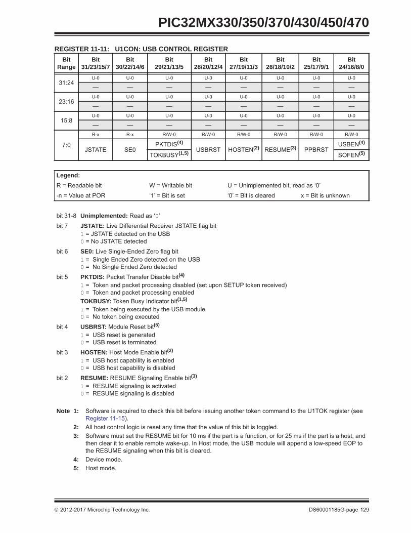
2012-2017 Microchip Technology Inc. DS60001185G-page 129
PIC32MX330/350/370/430/450/470
REGISTER 11-11: U1CON: USB CONTROL REGISTER Bit
RangeBit
31/23/15/7Bit
30/22/14/6Bit
29/21/13/5Bit
28/20/12/4Bit
27/19/11/3Bit
26/18/10/2Bit
25/17/9/1Bit
24/16/8/0
31:24U-0 U-0 U-0 U-0 U-0 U-0 U-0 U-0
— — — — — — — —
23:16U-0 U-0 U-0 U-0 U-0 U-0 U-0 U-0
— — — — — — — —
15:8U-0 U-0 U-0 U-0 U-0 U-0 U-0 U-0
— — — — — — — —
7:0
R-x R-x R/W-0 R/W-0 R/W-0 R/W-0 R/W-0 R/W-0
JSTATE SE0PKTDIS(4)
USBRST HOSTEN(2) RESUME(3) PPBRSTUSBEN(4)
TOKBUSY(1,5) SOFEN(5)
Legend:R = Readable bit W = Writable bit U = Unimplemented bit, read as ‘0’
-n = Value at POR ‘1’ = Bit is set ‘0’ = Bit is cleared x = Bit is unknown
bit 31-8 Unimplemented: Read as ‘0’
bit 7 JSTATE: Live Differential Receiver JSTATE flag bit1 = JSTATE detected on the USB0 = No JSTATE detected
bit 6 SE0: Live Single-Ended Zero flag bit1 = Single Ended Zero detected on the USB0 = No Single Ended Zero detected
bit 5 PKTDIS: Packet Transfer Disable bit(4)
1 = Token and packet processing disabled (set upon SETUP token received)0 = Token and packet processing enabledTOKBUSY: Token Busy Indicator bit(1,5)
1 = Token being executed by the USB module0 = No token being executed
bit 4 USBRST: Module Reset bit(5)
1 = USB reset is generated0 = USB reset is terminated
bit 3 HOSTEN: Host Mode Enable bit(2)
1 = USB host capability is enabled0 = USB host capability is disabled
bit 2 RESUME: RESUME Signaling Enable bit(3)
1 = RESUME signaling is activated0 = RESUME signaling is disabled
Note 1: Software is required to check this bit before issuing another token command to the U1TOK register (see Register 11-15).
2: All host control logic is reset any time that the value of this bit is toggled.3: Software must set the RESUME bit for 10 ms if the part is a function, or for 25 ms if the part is a host, and
then clear it to enable remote wake-up. In Host mode, the USB module will append a low-speed EOP to the RESUME signaling when this bit is cleared.
4: Device mode.5: Host mode.

PIC32MX330/350/370/430/450/470
DS60001185G-page 130 2012-2017 Microchip Technology Inc.
bit 1 PPBRST: Ping-Pong Buffers Reset bit1 = Reset all Even/Odd buffer pointers to the EVEN BD banks0 = Even/Odd buffer pointers not being Reset
bit 0 USBEN: USB Module Enable bit(4)
1 = USB module and supporting circuitry is enabled0 = USB module and supporting circuitry is disabledSOFEN: SOF Enable bit(5)
1 = SOF token sent every 1 ms0 = SOF token is disabled
REGISTER 11-11: U1CON: USB CONTROL REGISTER (CONTINUED)
Note 1: Software is required to check this bit before issuing another token command to the U1TOK register (see Register 11-15).
2: All host control logic is reset any time that the value of this bit is toggled.3: Software must set the RESUME bit for 10 ms if the part is a function, or for 25 ms if the part is a host, and
then clear it to enable remote wake-up. In Host mode, the USB module will append a low-speed EOP to the RESUME signaling when this bit is cleared.
4: Device mode.5: Host mode.

REGISTER 11-13: U1FRML: USB FRAME NUMBER LOW REGISTERBit
RangeBit
31/23/15/7Bit
30/22/14/6Bit
29/21/13/5Bit
28/20/12/4Bit
27/19/11/3Bit
26/18/10/2Bit
25/17/9/1Bit
24/16/8/0
31:24U-0 U-0 U-0 U-0 U-0 U-0 U-0 U-0
— — — — — — — —
23:16U-0 U-0 U-0 U-0 U-0 U-0 U-0 U-0
— — — — — — — —
15:8U-0 U-0 U-0 U-0 U-0 U-0 U-0 U-0
— — — — — — — —
7:0R-0 R-0 R-0 R-0 R-0 R-0 R-0 R-0
FRML<7:0>
Legend:R = Readable bit W = Writable bit U = Unimplemented bit, read as ‘0’
-n = Value at POR ‘1’ = Bit is set ‘0’ = Bit is cleared x = Bit is unknown
bit 31-8 Unimplemented: Read as ‘0’
bit 7-0 FRML<7:0>: The 11-bit Frame Number Lower bitsThe register bits are updated with the current frame number whenever a SOF TOKEN is received.
2012-2017 Microchip Technology Inc. DS60001185G-page 131
PIC32MX330/350/370/430/450/470
REGISTER 11-12: U1ADDR: USB ADDRESS REGISTERBit
RangeBit
31/23/15/7Bit
30/22/14/6Bit
29/21/13/5Bit
28/20/12/4Bit
27/19/11/3Bit
26/18/10/2Bit
25/17/9/1Bit
24/16/8/0
31:24U-0 U-0 U-0 U-0 U-0 U-0 U-0 U-0
— — — — — — — —
23:16U-0 U-0 U-0 U-0 U-0 U-0 U-0 U-0
— — — — — — — —
15:8U-0 U-0 U-0 U-0 U-0 U-0 U-0 U-0
— — — — — — — —
7:0R/W-0 R/W-0 R/W-0 R/W-0 R/W-0 R/W-0 R/W-0 R/W-0
LSPDEN DEVADDR<6:0>
Legend:R = Readable bit W = Writable bit U = Unimplemented bit, read as ‘0’
-n = Value at POR ‘1’ = Bit is set ‘0’ = Bit is cleared x = Bit is unknown
bit 31-8 Unimplemented: Read as ‘0’
bit 7 LSPDEN: Low Speed Enable Indicator bit1 = Next token command to be executed at Low Speed0 = Next token command to be executed at Full Speed
bit 6-0 DEVADDR<6:0>: 7-bit USB Device Address bits

REGISTER 11-15: U1TOK: USB TOKEN REGISTER Bit
RangeBit
31/23/15/7Bit
30/22/14/6Bit
29/21/13/5Bit
28/20/12/4Bit
27/19/11/3Bit
26/18/10/2Bit
25/17/9/1Bit
24/16/8/0
31:24U-0 U-0 U-0 U-0 U-0 U-0 U-0 U-0
— — — — — — — —
23:16U-0 U-0 U-0 U-0 U-0 U-0 U-0 U-0
— — — — — — — —
15:8U-0 U-0 U-0 U-0 U-0 U-0 U-0 U-0
— — — — — — — —
7:0R/W-0 R/W-0 R/W-0 R/W-0 R/W-0 R/W-0 R/W-0 R/W-0
PID<3:0>(1) EP<3:0>
Legend:R = Readable bit W = Writable bit U = Unimplemented bit, read as ‘0’-n = Value at POR ‘1’ = Bit is set ‘0’ = Bit is cleared x = Bit is unknown
bit 31-8 Unimplemented: Read as ‘0’bit 7-4 PID<3:0>: Token Type Indicator bits(1)
0001 = OUT (TX) token type transaction1001 = IN (RX) token type transaction1101 = SETUP (TX) token type transactionNote: All other values are reserved and must not be used.
bit 3-0 EP<3:0>: Token Command Endpoint Address bits The four bit value must specify a valid endpoint.
Note 1: All other values are reserved and must not be used.
PIC32MX330/350/370/430/450/470
DS60001185G-page 132 2012-2017 Microchip Technology Inc.
REGISTER 11-14: U1FRMH: USB FRAME NUMBER HIGH REGISTERBit
RangeBit
31/23/15/7Bit
30/22/14/6Bit
29/21/13/5Bit
28/20/12/4Bit
27/19/11/3Bit
26/18/10/2Bit
25/17/9/1Bit
24/16/8/0
31:24U-0 U-0 U-0 U-0 U-0 U-0 U-0 U-0
— — — — — — — —
23:16U-0 U-0 U-0 U-0 U-0 U-0 U-0 U-0
— — — — — — — —
15:8U-0 U-0 U-0 U-0 U-0 U-0 U-0 U-0
— — — — — — — —
7:0U-0 U-0 U-0 U-0 U-0 R-0 R-0 R-0
— — — — — FRMH<2:0>
Legend:R = Readable bit W = Writable bit U = Unimplemented bit, read as ‘0’
-n = Value at POR ‘1’ = Bit is set ‘0’ = Bit is cleared x = Bit is unknown
bit 31-3 Unimplemented: Read as ‘0’
bit 2-0 FRMH<2:0>: The Upper 3 bits of the Frame Numbers bitsThe register bits are updated with the current frame number whenever a SOF TOKEN is received.

REGISTER 11-17: U1BDTP1: USB BDT PAGE 1 REGISTER Bit
RangeBit
31/23/15/7Bit
30/22/14/6Bit
29/21/13/5Bit
28/20/12/4Bit
27/19/11/3Bit
26/18/10/2Bit
25/17/9/1Bit
24/16/8/0
31:24U-0 U-0 U-0 U-0 U-0 U-0 U-0 U-0
— — — — — — — —
23:16U-0 U-0 U-0 U-0 U-0 U-0 U-0 U-0
— — — — — — — —
15:8U-0 U-0 U-0 U-0 U-0 U-0 U-0 U-0
— — — — — — — —
7:0R/W-0 R/W-0 R/W-0 R/W-0 R/W-0 R/W-0 R/W-0 U-0
BDTPTRL<15:9> —
Legend:R = Readable bit W = Writable bit U = Unimplemented bit, read as ‘0’
-n = Value at POR ‘1’ = Bit is set ‘0’ = Bit is cleared x = Bit is unknown
bit 31-8 Unimplemented: Read as ‘0’
bit 7-1 BDTPTRL<15:9>: BDT Base Address bitsThis 7-bit value provides address bits 15 through 9 of the BDT base address, which defines the starting location of the BDT in system memory. The 32-bit BDT base address is 512-byte aligned.
bit 0 Unimplemented: Read as ‘0’
2012-2017 Microchip Technology Inc. DS60001185G-page 133
PIC32MX330/350/370/430/450/470
REGISTER 11-16: U1SOF: USB SOF THRESHOLD REGISTERBit
RangeBit
31/23/15/7Bit
30/22/14/6Bit
29/21/13/5Bit
28/20/12/4Bit
27/19/11/3Bit
26/18/10/2Bit
25/17/9/1Bit
24/16/8/0
31:24U-0 U-0 U-0 U-0 U-0 U-0 U-0 U-0
— — — — — — — —
23:16U-0 U-0 U-0 U-0 U-0 U-0 U-0 U-0
— — — — — — — —
15:8U-0 U-0 U-0 U-0 U-0 U-0 U-0 U-0
— — — — — — — —
7:0R/W-0 R/W-0 R/W-0 R/W-0 R/W-0 R/W-0 R/W-0 R/W-0
CNT<7:0>
Legend:R = Readable bit W = Writable bit U = Unimplemented bit, read as ‘0’
-n = Value at POR ‘1’ = Bit is set ‘0’ = Bit is cleared x = Bit is unknown
bit 31-8 Unimplemented: Read as ‘0’
bit 7-0 CNT<7:0>: SOF Threshold Value bitsTypical values of the threshold are:01001010 = 64-byte packet00101010 = 32-byte packet00011010 = 16-byte packet00010010 = 8-byte packet

REGISTER 11-19: U1BDTP3: USB BDT PAGE 3 REGISTER Bit
RangeBit
31/23/15/7Bit
30/22/14/6Bit
29/21/13/5Bit
28/20/12/4Bit
27/19/11/3Bit
26/18/10/2Bit
25/17/9/1Bit
24/16/8/0
31:24U-0 U-0 U-0 U-0 U-0 U-0 U-0 U-0
— — — — — — — —
23:16U-0 U-0 U-0 U-0 U-0 U-0 U-0 U-0
— — — — — — — —
15:8U-0 U-0 U-0 U-0 U-0 U-0 U-0 U-0
— — — — — — — —
7:0R/W-0 R/W-0 R/W-0 R/W-0 R/W-0 R/W-0 R/W-0 R/W-0
BDTPTRU<31:24>
Legend:R = Readable bit W = Writable bit U = Unimplemented bit, read as ‘0’
-n = Value at POR ‘1’ = Bit is set ‘0’ = Bit is cleared x = Bit is unknown
Unimplemented: Read as ‘0’
BDTPTRU<31:24>: BDT Base Address bitsThis 8-bit value provides address bits 31 through 24 of the BDT base address, defines the starting location of the BDT in system memory. The 32-bit BDT base address is 512-byte aligned.
PIC32MX330/350/370/430/450/470
DS60001185G-page 134 2012-2017 Microchip Technology Inc.
REGISTER 11-18: U1BDTP2: USB BDT PAGE 2 REGISTER Bit
RangeBit
31/23/15/7Bit
30/22/14/6Bit
29/21/13/5Bit
28/20/12/4Bit
27/19/11/3Bit
26/18/10/2Bit
25/17/9/1Bit
24/16/8/0
31:24U-0 U-0 U-0 U-0 U-0 U-0 U-0 U-0
— — — — — — — —
23:16U-0 U-0 U-0 U-0 U-0 U-0 U-0 U-0
— — — — — — — —
15:8U-0 U-0 U-0 U-0 U-0 U-0 U-0 U-0
— — — — — — — —
7:0R/W-0 R/W-0 R/W-0 R/W-0 R/W-0 R/W-0 R/W-0 R/W-0
BDTPTRH<23:16>
Legend:R = Readable bit W = Writable bit U = Unimplemented bit, read as ‘0’
-n = Value at POR ‘1’ = Bit is set ‘0’ = Bit is cleared x = Bit is unknown
bit 31-8 Unimplemented: Read as ‘0’
bit 7-0 BDTPTRH<23:16>: BDT Base Address bitsThis 8-bit value provides address bits 23 through 16 of the BDT base address, which defines the starting location of the BDT in system memory. The 32-bit BDT base address is 512-byte aligned.
bit 31-8
bit 7-0
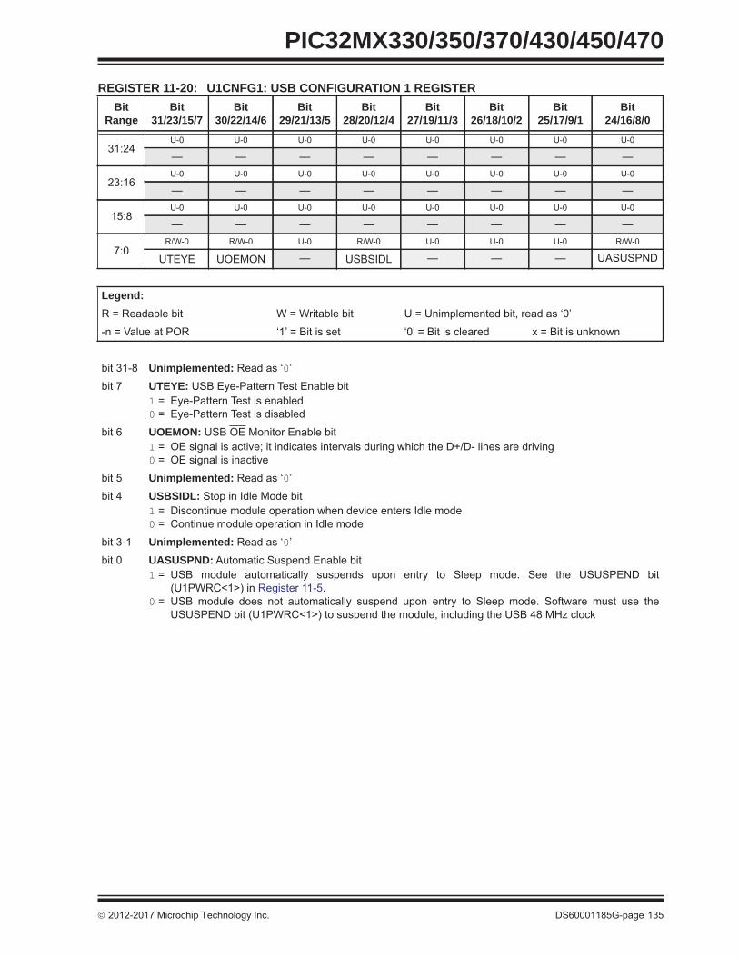
2012-2017 Microchip Technology Inc. DS60001185G-page 135
PIC32MX330/350/370/430/450/470
REGISTER 11-20: U1CNFG1: USB CONFIGURATION 1 REGISTER Bit
RangeBit
31/23/15/7Bit
30/22/14/6Bit
29/21/13/5Bit
28/20/12/4Bit
27/19/11/3Bit
26/18/10/2Bit
25/17/9/1Bit
24/16/8/0
31:24U-0 U-0 U-0 U-0 U-0 U-0 U-0 U-0
— — — — — — — —
23:16U-0 U-0 U-0 U-0 U-0 U-0 U-0 U-0
— — — — — — — —
15:8U-0 U-0 U-0 U-0 U-0 U-0 U-0 U-0
— — — — — — — —
7:0R/W-0 R/W-0 U-0 R/W-0 U-0 U-0 U-0 R/W-0
UTEYE UOEMON — USBSIDL — — — UASUSPND
Legend:R = Readable bit W = Writable bit U = Unimplemented bit, read as ‘0’
-n = Value at POR ‘1’ = Bit is set ‘0’ = Bit is cleared x = Bit is unknown
bit 31-8 Unimplemented: Read as ‘0’
bit 7 UTEYE: USB Eye-Pattern Test Enable bit1 = Eye-Pattern Test is enabled0 = Eye-Pattern Test is disabled
bit 6 UOEMON: USB OE Monitor Enable bit1 = OE signal is active; it indicates intervals during which the D+/D- lines are driving0 = OE signal is inactive
bit 5 Unimplemented: Read as ‘0’
bit 4 USBSIDL: Stop in Idle Mode bit1 = Discontinue module operation when device enters Idle mode0 = Continue module operation in Idle mode
bit 3-1 Unimplemented: Read as ‘0’
bit 0 UASUSPND: Automatic Suspend Enable bit1 = USB module automatically suspends upon entry to Sleep mode. See the USUSPEND bit
(U1PWRC<1>) in Register 11-5.0 = USB module does not automatically suspend upon entry to Sleep mode. Software must use the
USUSPEND bit (U1PWRC<1>) to suspend the module, including the USB 48 MHz clock

PIC32MX330/350/370/430/450/470
DS60001185G-page 136 2012-2017 Microchip Technology Inc.
REGISTER 11-21: U1EP0-U1EP15: USB ENDPOINT CONTROL REGISTER Bit
RangeBit
31/23/15/7Bit
30/22/14/6Bit
29/21/13/5Bit
28/20/12/4Bit
27/19/11/3Bit
26/18/10/2Bit
25/17/9/1Bit
24/16/8/0
31:24U-0 U-0 U-0 U-0 U-0 U-0 U-0 U-0
— — — — — — — —
23:16U-0 U-0 U-0 U-0 U-0 U-0 U-0 U-0
— — — — — — — —
15:8U-0 U-0 U-0 U-0 U-0 U-0 U-0 U-0
— — — — — — — —
7:0R/W-0 R/W-0 U-0 R/W-0 R/W-0 R/W-0 R/W-0 R/W-0
LSPD RETRYDIS — EPCONDIS EPRXEN EPTXEN EPSTALL EPHSHK
Legend:R = Readable bit W = Writable bit U = Unimplemented bit, read as ‘0’
-n = Value at POR ‘1’ = Bit is set ‘0’ = Bit is cleared x = Bit is unknown
bit 31-8 Unimplemented: Read as ‘0’
bit 7 LSPD: Low-Speed Direct Connection Enable bit (Host mode and U1EP0 only)1 = Direct connection to a low-speed device is enabled0 = Direct connection to a low-speed device is disabled; hub required with PRE_PID
bit 6 RETRYDIS: Retry Disable bit (Host mode and U1EP0 only)1 = Retry NAKed transactions is disabled0 = Retry NAKed transactions is enabled; retry done in hardware
bit 5 Unimplemented: Read as ‘0’
bit 4 EPCONDIS: Bidirectional Endpoint Control bitIf EPTXEN = 1 and EPRXEN = 1:1 = Disable Endpoint n from Control transfers; only TX and RX transfers allowed0 = Enable Endpoint n for Control (SETUP) transfers; TX and RX transfers also allowedOtherwise, this bit is ignored.
bit 3 EPRXEN: Endpoint Receive Enable bit1 = Endpoint n receive is enabled0 = Endpoint n receive is disabled
bit 2 EPTXEN: Endpoint Transmit Enable bit1 = Endpoint n transmit is enabled0 = Endpoint n transmit is disabled
bit 1 EPSTALL: Endpoint Stall Status bit1 = Endpoint n was stalled0 = Endpoint n was not stalled
bit 0 EPHSHK: Endpoint Handshake Enable bit1 = Endpoint Handshake is enabled0 = Endpoint Handshake is disabled (typically used for isochronous endpoints)

2012-2017 Microchip Technology Inc. DS60001185G-page 137
PIC32MX330/350/370/430/450/470
12.0 I/O PORTSNote: This data sheet summarizes the features
of the PIC32MX330/350/370/430/450/470 family of devices. It is not intended to be a comprehensive reference source. To complement the information in this data sheet, refer to Section 12. “I/O Ports”(DS60001120), which is available from the Documentation > Reference Manual section of the Microchip PIC32 web site (www.microchip.com/pic32).
General purpose I/O pins are the simplest of peripher-als. They allow the PIC® MCU to monitor and control other devices. To add flexibility and functionality, some pins are multiplexed with alternate function(s). These functions depend on which peripheral features are on the device. In general, when a peripheral is functioning, that pin may not be used as a general purpose I/O pin.
Following are key features of the I/O Port module:• Individual output pin open-drain enable/disable• Individual input pin weak pull-up and pull-down• Monitor selective inputs and generate interrupt
when change in pin state is detected• Operation during CPU Sleep and Idle modes• Fast bit manipulation using CLR, SET, and INV
registersFigure 12-1 illustrates a block diagram of a typical multiplexed I/O port.
FIGURE 12-1: BLOCK DIAGRAM OF A TYPICAL MULTIPLEXED PORT STRUCTURE
Peripheral Output Data
Peripheral Module
Peripheral Output Enable
PIO Module
Peripheral Module Enable
WR LAT
I/O Pin
WR PORT
Data Bus
RD LAT
RD PORT
RD TRIS
WR TRIS
0
1
RD ODC
PBCLK
QD
CKEN Q
QD
CKEN Q
QD
CKEN Q
Q D
CKQ
Q D
CKQ
0
1
PBCLK
WR ODC
ODC
TRIS
LAT
Sleep
1
0
1
0
Output Multiplexers
I/O Cell
SynchronizationRPeripheral Input
Legend: R = Peripheral input buffer types may vary. Refer to Table 1-1 for peripheral details.Note: This block diagram is a general representation of a shared port/peripheral structure for illustration purposes only. The actual structure
for any specific port/peripheral combination may be different than it is shown here.
Peripheral Input Buffer

PIC32MX330/350/370/430/450/470
DS60001185G-page 138 2012-2017 Microchip Technology Inc.
12.1 Parallel I/O (PIO) PortsAll port pins have ten registers directly associated with their operation as digital I/O. The data direction register (TRISx) determines whether the pin is an input or an output. If the data direction bit is a ‘1’, then the pin is an input. All port pins are defined as inputs after a Reset. Reads from the latch (LATx) read the latch. Writes to the latch write the latch. Reads from the port (PORTx) read the port pins, while writes to the port pins write the latch.
12.1.1 OPEN-DRAIN CONFIGURATIONIn addition to the PORTx, LATx, and TRISx registers for data control, some port pins can also be individually configured for either digital or open-drain output. This is controlled by the Open-Drain Control register, ODCx, associated with each port. Setting any of the bits con-figures the corresponding pin to act as an open-drain output.
The open-drain feature allows the presence of outputs higher than VDD (e.g., 5V) on any desired 5V-tolerant pins by using external pull-up resistors. The maximum open-drain voltage allowed is the same as the maxi-mum VIH specification.
See the “Device Pin Tables” section for the available pins and their functionality.
12.1.2 CONFIGURING ANALOG AND DIGITAL PORT PINS
The ANSELx register controls the operation of the analog port pins. The port pins that are to function as analog inputs must have their corresponding ANSEL and TRIS bits set. In order to use port pins for I/O functionality with digital modules, such as Timers, UARTs, etc., the corresponding ANSELx bit must be cleared.
The ANSELx register has a default value of 0xFFFF; therefore, all pins that share analog functions are analog (not digital) by default.
If the TRIS bit is cleared (output) while the ANSELx bit is set, the digital output level (VOH or VOL) is converted by an analog peripheral, such as the ADC module or Comparator module.
When the PORT register is read, all pins configured as analog input channels are read as cleared (a low level).
Pins configured as digital inputs do not convert an analog input. Analog levels on any pin defined as a digital input (including the ANx pins) can cause the input buffer to consume current that exceeds the device specifications.
12.1.3 I/O PORT WRITE/READ TIMINGOne instruction cycle is required between a port direction change or port write operation and a read operation of the same port. Typically this instruction would be an NOP.
12.1.4 INPUT CHANGE NOTIFICATIONThe input change notification function of the I/O ports allows the PIC32MX330/350/370/430/450/470 devices to generate interrupt requests to the processor in response to a change-of-state on selected input pins. This feature can detect input change-of-states even in Sleep mode, when the clocks are disabled. Every I/O port pin can be selected (enabled) for generating an interrupt request on a change-of-state.
Five control registers are associated with the CN func-tionality of each I/O port. The CNENx registers contain the CN interrupt enable control bits for each of the input pins. Setting any of these bits enables a CN interrupt for the corresponding pins.
The CNSTATx register indicates whether a change occurred on the corresponding pin since the last read of the PORTx bit.
Each I/O pin also has a weak pull-up and every I/O pin has a weak pull-down connected to it. The pull-ups act as a current source or sink source connected to the pin, and eliminate the need for external resistors when push-button or keypad devices are connected. The pull-ups and pull-downs are enabled separately using the CNPUx and the CNPDx registers, which contain the control bits for each of the pins. Setting any of the control bits enables the weak pull-ups and/or pull-downs for the corresponding pins.
An additional control register (CNCONx) is shown in Register 12-3.
12.2 CLR, SET, and INV RegistersEvery I/O module register has a corresponding CLR (clear), SET (set) and INV (invert) register designed to provide fast atomic bit manipulations. As the name of the register implies, a value written to a SET, CLR or INV register effectively performs the implied operation, but only on the corresponding base register and only bits specified as ‘1’ are modified. Bits specified as ‘0’ are not modified.
Reading SET, CLR and INV registers returns undefined values. To see the affects of a write operation to a SET, CLR or INV register, the base register must be read.
Note: Pull-ups and pull-downs on change notifi-cation pins should always be disabled when the port pin is configured as a digital output. They should also be disabled on 5V tolerant pins when the pin voltage can exceed VDD.

2012-2017 Microchip Technology Inc. DS60001185G-page 139
PIC32MX330/350/370/430/450/47012.3 Peripheral Pin SelectA major challenge in general purpose devices is provid-ing the largest possible set of peripheral features while minimizing the conflict of features on I/O pins. The chal-lenge is even greater on low pin count devices. In an application where more than one peripheral needs to be assigned to a single pin, inconvenient workarounds in application code or a complete redesign may be the only options.
Peripheral pin select configuration provides an alternative to these choices by enabling peripheral set selection and their placement on a wide range of I/O pins. By increasing the pinout options available on a particular device, users can better tailor the device to their entire application, rather than trimming the application to fit the device.
The peripheral pin select configuration feature operates over a fixed subset of digital I/O pins. Users may independently map the input and/or output of most digital peripherals to these I/O pins. Peripheral pin select is performed in software and generally does not require the device to be reprogrammed. Hardware safeguards are included that prevent accidental or spurious changes to the peripheral mapping once it has been established.
12.3.1 AVAILABLE PINSThe number of available pins is dependent on the particular device and its pin count. Pins that support the peripheral pin select feature include the designation “RPn” in their full pin designation, where “RP” designates a remappable peripheral and “n” is the remappable port number.
12.3.2 AVAILABLE PERIPHERALSThe peripherals managed by the peripheral pin select are all digital-only peripherals. These include general serial communications (UART and SPI), general pur-pose timer clock inputs, timer-related peripherals (input capture and output compare) and interrupt-on-change inputs.
In comparison, some digital-only peripheral modules are never included in the peripheral pin select feature. This is because the peripheral’s function requires spe-cial I/O circuitry on a specific port and cannot be easily connected to multiple pins. These modules include I2C among others. A similar requirement excludes all mod-ules with analog inputs, such as the Analog-to-Digital Converter (ADC).
A key difference between remappable and non-remap-pable peripherals is that remappable peripherals are not associated with a default I/O pin. The peripheral must always be assigned to a specific I/O pin before it can be used. In contrast, non-remappable peripherals are always available on a default pin, assuming that the peripheral is active and not conflicting with another peripheral.
When a remappable peripheral is active on a given I/O pin, it takes priority over all other digital I/O and digital communication peripherals associated with the pin. Priority is given regardless of the type of peripheral that is mapped. Remappable peripherals never take priority over any analog functions associated with the pin.
12.3.3 CONTROLLING PERIPHERAL PIN SELECT
Peripheral pin select features are controlled through two sets of SFRs: one to map peripheral inputs, and one to map outputs. Because they are separately controlled, a particular peripheral’s input and output (if the peripheral has both) can be placed on any selectable function pin without constraint.
The association of a peripheral to a peripheral-select-able pin is handled in two different ways, depending on whether an input or output is being mapped.
12.3.4 INPUT MAPPINGThe inputs of the peripheral pin select options are mapped on the basis of the peripheral. That is, a control register associated with a peripheral dictates the pin it will be mapped to. The [pin name]R registers, where [pin name] refers to the peripheral pins listed in Table 12-1, are used to configure peripheral input mapping (see Register 12-1). Each register contains sets of 4 bit fields. Programming these bit fields with an appropriate value maps the RPn pin with the corresponding value to that peripheral. For any given device, the valid range of values for any bit field is shown in Table 12-1.
For example, Figure 12-2 illustrates the remappable pin selection for the U1RX input.
FIGURE 12-2: REMAPPABLE INPUT EXAMPLE FOR U1RX
RPA2
RPB6
RPA4
0
1
2 U1RX input
U1RXR<3:0>
to peripheral
RPnn
Note: For input only, peripheral pin select functionality does not have priority over TRISx settings. Therefore, when configuring RPn pin for input, the corresponding bit in the TRISx register must also be configured for input (set to ‘1’).
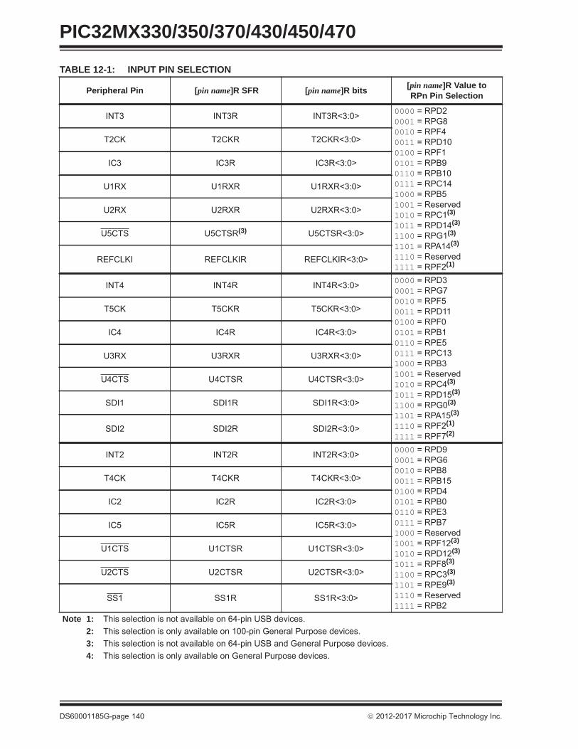
PIC32MX330/350/370/430/450/470
DS60001185G-page 140 2012-2017 Microchip Technology Inc.
TABLE 12-1: INPUT PIN SELECTION
Peripheral Pin [pin name]R SFR [pin name]R bits [pin name]R Value to RPn Pin Selection
INT3 INT3R INT3R<3:0> 0000 = RPD20001 = RPG80010 = RPF40011 = RPD100100 = RPF10101 = RPB90110 = RPB100111 = RPC141000 = RPB51001 = Reserved1010 = RPC1(3)
1011 = RPD14(3)
1100 = RPG1(3)
1101 = RPA14(3)
1110 = Reserved1111 = RPF2(1)
T2CK T2CKR T2CKR<3:0>
IC3 IC3R IC3R<3:0>
U1RX U1RXR U1RXR<3:0>
U2RX U2RXR U2RXR<3:0>
U5CTS U5CTSR(3) U5CTSR<3:0>
REFCLKI REFCLKIR REFCLKIR<3:0>
INT4 INT4R INT4R<3:0> 0000 = RPD30001 = RPG70010 = RPF50011 = RPD110100 = RPF00101 = RPB10110 = RPE50111 = RPC131000 = RPB31001 = Reserved1010 = RPC4(3)
1011 = RPD15(3)
1100 = RPG0(3)
1101 = RPA15(3)
1110 = RPF2(1)
1111 = RPF7(2)
T5CK T5CKR T5CKR<3:0>
IC4 IC4R IC4R<3:0>
U3RX U3RXR U3RXR<3:0>
U4CTS U4CTSR U4CTSR<3:0>
SDI1 SDI1R SDI1R<3:0>
SDI2 SDI2R SDI2R<3:0>
INT2 INT2R INT2R<3:0> 0000 = RPD90001 = RPG60010 = RPB80011 = RPB150100 = RPD40101 = RPB00110 = RPE30111 = RPB71000 = Reserved1001 = RPF12(3)
1010 = RPD12(3)
1011 = RPF8(3)
1100 = RPC3(3)
1101 = RPE9(3)
1110 = Reserved1111 = RPB2
T4CK T4CKR T4CKR<3:0>
IC2 IC2R IC2R<3:0>
IC5 IC5R IC5R<3:0>
U1CTS U1CTSR U1CTSR<3:0>
U2CTS U2CTSR U2CTSR<3:0>
SS1 SS1R SS1R<3:0>
Note 1: This selection is not available on 64-pin USB devices.2: This selection is only available on 100-pin General Purpose devices.3: This selection is not available on 64-pin USB and General Purpose devices.4: This selection is only available on General Purpose devices.

2012-2017 Microchip Technology Inc. DS60001185G-page 141
PIC32MX330/350/370/430/450/470
INT1 INT1R INT1R<3:0> 0000 = RPD10001 = RPG90010 = RPB140011 = RPD00100 = RPD80101 = RPB60110 = RPD50111 = RPB21000 = RPF3(4)
1001 = RPF13(3)
1010 = Reserved1011 = RPF2(1)
1100 = RPC2(3)
1101 = RPE8(3)
1110 = Reserved1111 = Reserved
T3CK T3CKR T3CKR<3:0>
IC1 IC1R IC1R<3:0>
U3CTS U3CTSR U3CTSR<3:0>
U4RX U4RXR U4RXR<3:0>
U5RX U5RXR(3) U5RXR<3:0>
SS2 SS2R SS2R<3:0>
OCFA OCFAR OCFAR<3:0>
TABLE 12-1: INPUT PIN SELECTION (CONTINUED)
Peripheral Pin [pin name]R SFR [pin name]R bits [pin name]R Value to RPn Pin Selection
Note 1: This selection is not available on 64-pin USB devices.2: This selection is only available on 100-pin General Purpose devices.3: This selection is not available on 64-pin USB and General Purpose devices.4: This selection is only available on General Purpose devices.

PIC32MX330/350/370/430/450/470
DS60001185G-page 142 2012-2017 Microchip Technology Inc.
12.3.5 OUTPUT MAPPINGIn contrast to inputs, the outputs of the peripheral pin select options are mapped on the basis of the pin. In this case, a control register associated with a particular pin dictates the peripheral output to be mapped. The RPnR registers (Register 12-2) are used to control output mapping. Like the [pin name]Rregisters, each register contains sets of 4 bit fields. The value of the bit field corresponds to one of the peripherals, and that peripheral’s output is mapped to the pin (see Table 12-2 and Figure 12-3).
A null output is associated with the output register reset value of ‘0’. This is done to ensure that remappable outputs remain disconnected from all output pins by default.
FIGURE 12-3: EXAMPLE OF MULTIPLEXING OF REMAPPABLE OUTPUT FOR RPA0
RPA0R<3:0>
0
15
1
Default
U1TX Output
U1RTS Output 2
14
Output DataRPA0
12.3.6 CONTROLLING CONFIGURATION CHANGES
Because peripheral remapping can be changed during run time, some restrictions on peripheral remapping are needed to prevent accidental configuration changes. PIC32 devices include two features to prevent alterations to the peripheral map:
• Control register lock sequence• Configuration bit select lock
12.3.6.1 Control Register LockUnder normal operation, writes to the RPnR and [pin name]R registers are not allowed. Attempted writes appear to execute normally, but the contents of the registers remain unchanged. To change these regis-ters, they must be unlocked in hardware. The regis-ter lock is controlled by the IOLOCK Configuration bit (CFGCON<13>). Setting IOLOCK prevents writes to the control registers; clearing IOLOCK allows writes.
To set or clear the IOLOCK bit, an unlock sequence must be executed. Refer to Section 6. “Oscillator”(DS60001112) in the “PIC32 Family Reference Manual” for details.
12.3.6.2 Configuration Bit Select LockAs an additional level of safety, the device can be configured to prevent more than one write session to the RPnR and [pin name]R registers. The IOL1WAY Configuration bit (DEVCFG3<29>) blocks the IOLOCK bit from being cleared after it has been set once. If IOLOCK remains set, the register unlock procedure does not execute, and the peripheral pin select control registers cannot be written to. The only way to clear the bit and re-enable peripheral remapping is to perform a device Reset.
In the default (unprogrammed) state, IOL1WAY is set, restricting users to one write session.

2012-2017 Microchip Technology Inc. DS60001185G-page 143
PIC32MX330/350/370/430/450/470
TABLE 12-2: OUTPUT PIN SELECTION
RPn Port Pin RPnR SFR RPnR bits RPnR Value to Peripheral Selection
RPD2 RPD2R RPD2R<3:0> 0000 = No Connect0001 = U3TX0010 = U4RTS0011 = Reserved0100 = Reserved0101 = Reserved0110 = SDO20111 = Reserved1000 = Reserved1001 = Reserved1010 = Reserved1011 = OC31100 = Reserved1101 = C2OUT1110 = Reserved1111 = Reserved
RPG8 RPG8R RPG8R<3:0>
RPF4 RPF4R RPF4R<3:0>
RPD10 RPD10R RPD10R<3:0>
RPF1 RPF1R RPF1R<3:0>
RPB9 RPB9R RPB9R<3:0>
RPB10 RPB10R RPB10R<3:0>
RPC14 RPC14R RPC14R<3:0>
RPB5 RPB5R RPB5R<3:0>
RPC1(4) RPC1R RPC1R<3:0>
RPD14(4) RPD14R RPD14R<3:0>
RPG1(4) RPG1R RPG1R<3:0>
RPA14(4) RPA14R RPA14R<3:0>
RPD3 RPD3R RPD3R<3:0> 0000 = No Connect0001 = U2TX0010 = Reserved0011 = U1TX0100 = U5RTS(4)
0101 = Reserved0110 = SDO20111 = Reserved1000 = SDO11001 = Reserved1010 = Reserved1011 = OC41100 = Reserved1101 = Reserved1110 = Reserved1111 = Reserved
RPG7 RPG7R RPG7R<3:0>
RPF5 RPF5R RPF5R<3:0>
RPD11 RPD11R RPD11R<3:0>
RPF0 RPF0R RPF0R<3:0>
RPB1 RPB1R RPB1R<3:0>
RPE5 RPE5R RPE5R<3:0>
RPC13 RPC13R RPC13R<3:0>
RPB3 RPB3R RPB3R<3:0>
RPF3(2) RPF3R RPF3R<3:0>
RPC4(4) RPC4R RPC4R<3:0>
RPD15(4) RPD15R RPD15R<3:0>
RPG0(4) RPG0R RPG0R<3:0>
RPA15(4) RPA15R RPA15R<3:0>Note 1: This selection is only available on General Purpose devices.
2: This selection is only available on 64-pin General Purpose devices.3: This selection is only available on 100-pin General Purpose devices.4: This selection is only available on 100-pin USB and General Purpose devices.5: This selection is not available on 64-pin USB devices.

PIC32MX330/350/370/430/450/470
DS60001185G-page 144 2012-2017 Microchip Technology Inc.
RPD9 RPD9R RPD9R<3:0> 0000 = No Connect0001 = U3RTS0010 = U4TX0011 = REFCLKO0100 = U5TX(4)
0101 = Reserved0110 = Reserved0111 = SS11000 = SDO11001 = Reserved1010 = Reserved1011 = OC51100 = Reserved1101 = C1OUT1110 = Reserved1111 = Reserved
RPG6 RPG6R RPG6R<3:0>
RPB8 RPB8R RPB8R<3:0>
RPB15 RPB15R RPB15R<3:0>
RPD4 RPD4R RPD4R<3:0>
RPB0 RPB0R RPB0R<3:0>
RPE3 RPE3R RPE3R<3:0>
RPB7 RPB7R RPB7R<3:0>
RPB2 RPB2R RPB2R<3:0>
RPF12(4) RPF12R RPF12R<3:0>
RPD12(4) RPD12R RPD12R<3:0>
RPF8(4) RPF8R RPF8R<3:0>
RPC3(4) RPC3R RPC3R<3:0>
RPE9(4) RPE9R RPE9R<3:0>
RPD1 RPD1R RPD1R<3:0> 0000 = No Connect0001 = U2RTS0010 = Reserved0011 = U1RTS0100 = U5TX(4)
0101 = Reserved0110 = SS20111 = Reserved1000 = SDO11001 = Reserved1010 = Reserved1011 = OC21100 = OC11101 = Reserved1110 = Reserved1111 = Reserved
RPG9 RPG9R RPG9R<3:0>
RPB14 RPB14R RPB14R<3:0>
RPD0 RPD0R RPD0R<3:0>
RPD8 RPD8R RPD8R<3:0>
RPB6 RPB6R RPB6R<3:0>
RPD5 RPD5R RPD5R<3:0>
RPF3(3) RPF3R RPF3R<3:0>
RPF6(1) RPF6R RPF6R<3:0>
RPF13(4) RPF13R RPF13R<3:0>
RPC2(4) RPC2R RPC2R<3:0>
RPE8(4) RPE8R RPE8R<3:0>
RPF2(5) RPF2R RPF2R<3:0>
TABLE 12-2: OUTPUT PIN SELECTION (CONTINUED)
RPn Port Pin RPnR SFR RPnR bits RPnR Value to Peripheral Selection
Note 1: This selection is only available on General Purpose devices.2: This selection is only available on 64-pin General Purpose devices.3: This selection is only available on 100-pin General Purpose devices.4: This selection is only available on 100-pin USB and General Purpose devices.5: This selection is not available on 64-pin USB devices.

2012-2017 M
icrochip Technology Inc.D
S60001185G
-page
145
PIC32M
X330/350/370/430/450/470
12.4 Control Registers
TABLE 12-3: PORTA REGISTER MAP FOR PIC32MX330F064L, PIC32MX350F128L, PIC32MX350F256L, PIC32MX370F512L, PIC32MX430F064L, PIC32MX450F128L, PIC32MX450F256L, AND PIC32MX470F512L DEVICES ONLY
Virtu
al A
ddre
ss(B
F88_
#)
Reg
iste
rN
ame(1
)
Bit
Ran
geBits
All
Res
ets
31/15 30/14 29/13 28/12 27/11 26/10 25/9 24/8 23/7 22/6 21/5 20/4 19/3 18/2 17/1 16/0
6000 ANSELA31:16 — — — — — — — — — — — — — — — — 0000
15:0 — — — — — ANSELA10 ANSELA9 — — — — — — — — — 0060
6010 TRISA31:16 — — — — — — — — — — — — — — — — 0000
15:0 TRISA15 TRISA14 — — — TRISA10 TRISA9 — TRISA7 TRISA6 TRISA5 TRISA4 TRISA3 TRISA2 TRISA1 TRISA0 xxxx
6020 PORTA31:16 — — — — — — — — — — — — — — — — 0000
15:0 RA15 RA14 — — — RA10 RA9 — RA7 RA6 RA5 RA4 RA3 RA2 RA1 RA0 xxxx
6030 LATA31:16 — — — — — — — — — — — — — — — — 0000
15:0 LATA15 LATA14 — — — LATA10 LATA9 — LATA7 LATA6 LATA5 LATA4 LATA3 LATA2 LATA1 LATA0 xxxx
6040 ODCA31:16 — — — — — — — — — — — — — — — — 0000
15:0 ODCA15 ODCA14 — — — ODCA10 ODCA9 — ODCA7 ODCA6 ODCA5 ODCA4 ODCA3 ODCA2 ODCA1 ODCA0 xxxx
6050 CNPUA31:16 — — — — — — — — — — — — — — — — 0000
15:0 CNPUA15 CNPUA14 — — — CNPUA10 CNPUA9 — CNPUA7 CNPUA6 CNPUA5 CNPUA4 CNPUA3 CNPUA2 CNPUA1 CNPUA0 xxxx
6060 CNPDA31:16 — — — — — — — — — — — — — — — — 0000
15:0 CNPDA15 CNPDA14 — — — CNPDA10 CNPDA9 — CNPDA7 CNPDA6 CNPDA5 CNPDA4 CNPDA3 CNPDA2 CNPDA1 CNPDA0 xxxx
6070 CNCONA31:16 — — — — — — — — — — — — — — — — 0000
15:0 ON — SIDL — — — — — — — — — — — — — 0000
6080 CNENA31:16 — — — — — — — — — — — — — — — — 0000
15:0 CNIEA15 CNIEA14 — — — CNIEA10 CNIEA9 — CNIEA7 CNIEA6 CNIEA5 CNIEA4 CNIEA3 CNIEA2 CNIEA1 CNIEA0 xxxx
6090 CNSTATA31:16 — — — — — — — — — — — — — — — — 0000
15:0 CNSTATA15
CNSTATA14 — — — CN
STATA10CN
STATA9 — CNSTATA7
CNSTATA6
CNSTATA5
CNSTATA4
CNSTATA3
CNSTATA2
CNSTATA1
CNSTATA0
xxxx
Legend: x = Unknown value on Reset; — = Unimplemented, read as ‘0’; Reset values are shown in hexadecimal.Note 1: All registers in this table have corresponding CLR, SET and INV registers at its virtual address, plus an offset of 0x4, 0x8 and 0xC, respectively. See Section 12.2 “CLR, SET, and INV Registers” for
more information.

PIC32M
X330/350/370/430/450/470
DS
60001185G-page
146
2012-2017 M
icrochip Technology Inc.
TABLE 12-4: PORTB REGISTER MAPVi
rtual
Add
ress
(BF8
8_#)
Reg
iste
rN
ame(1
)
Bit
Ran
ge
Bits
All
Res
ets
31/15 30/14 29/13 28/12 27/11 26/10 25/9 24/8 23/7 22/6 21/5 20/4 19/3 18/2 17/1 16/0
6100 ANSELB31:16 — — — — — — — — — — — — — — — — 000015:0 ANSELB15 ANSELB14 ANSELB13 ANSELB12 ANSELB11 ANSELB10 ANSELB9 ANSELB8 ANSELB7 ANSELB6 ANSELB5 ANSELB4 ANSELB3 ANSELB2 ANSELB1 ANSELB0 FFFF
6110 TRISB31:16 — — — — — — — — — — — — — — — — 000015:0 TRISB15 TRISB14 TRISB13 TRISB12 TRISB11 TRISB10 TRISB9 TRISB8 TRISB7 TRISB6 TRISB5 TRISB4 TRISB3 TRISB2 TRISB1 TRISB0 xxxx
6120 PORTB31:16 — — — — — — — — — — — — — — — — 000015:0 RB15 RB14 RB13 RB12 RB11 RB10 RB9 RB8 RB7 RB6 RB5 RB4 RB3 RB2 RB1 RB0 xxxx
6130 LATB31:16 — — — — — — — — — — — — — — — — 000015:0 LATB15 LATB14 LATB13 LATB12 LATB11 LATB10 LATB9 LATB8 LATB7 LATB6 LATB5 LATB4 LATB3 LATB2 LATB1 LATB0 xxxx
6140 ODCB31:16 — — — — — — — — — — — — — — — — 000015:0 ODCB15 ODCB14 ODCB13 ODCB12 ODCB11 ODCB10 ODCB9 ODCB8 ODCB7 ODCB6 ODCB5 ODCB4 ODCB3 ODCB2 ODCB1 ODCB0 xxxx
6150 CNPUB31:16 — — — — — — — — — — — — — — — — 000015:0 CNPUB15 CNPUB14 CNPUB13 CNPUB12 CNPUB11 CNPUB10 CNPUB9 CNPUB8 CNPUB7 CNPUB6 CNPUB5 CNPUB4 CNPUB3 CNPUB2 CNPUB1 CNPUB0 xxxx
6160 CNPDB31:16 — — — — — — — — — — — — — — — — 000015:0 CNPDB15 CNPDB14 CNPDB13 CNPDB12 CNPDB11 CNPDB10 CNPDB9 CNPDB8 CNPDB7 CNPDB6 CNPDB5 CNPDB4 CNPDB3 CNPDB2 CNPDB1 CNPDB0 xxxx
6170 CNCONB31:16 — — — — — — — — — — — — — — — — 000015:0 ON — SIDL — — — — — — — — — — — — — 0000
6180 CNENB31:16 — — — — — — — — — — — — — — — — 000015:0 CNIEB15 CNIEB14 CNIEB13 CNIEB12 CNIEB11 CNIEB10 CNIEB9 CNIEB8 CNIEB7 CNIEB6 CNIEB5 CNIEB4 CNIEB3 CNIEB2 CNIEB1 CNIEB0 xxxx
6190 CNSTATB31:16 — — — — — — — — — — — — — — — — 0000
15:0 CNSTATB15
CNSTATB14
CNSTATB13
CNSTATB12
CNSTATB11
CNSTATB10
CNSTATB9
CNSTATB8
CNSTATB7
CNSTATB6
CNSTATB5
CNSTATB4
CNSTATB3
CNSTATB2
CNSTATB1
CNSTATB0 xxxx
Legend: x = Unknown value on Reset; — = Unimplemented, read as ‘0’; Reset values are shown in hexadecimal.Note 1: All registers in this table have corresponding CLR, SET and INV registers at its virtual address, plus an offset of 0x4, 0x8 and 0xC, respectively. See Section 12.2 “CLR, SET, and INV Registers” for
more information.

2012-2017 M
icrochip Technology Inc.D
S60001185G
-page
147
PIC32M
X330/350/370/430/450/470
TABLE 12-5: PORTC REGISTER MAP FOR PIC32MX330F064L, PIC32MX350F128L, PIC32MX350F256L, PIC32MX370F512L, PIC32MX430F064L, PIC32MX450F128L, PIC32MX450F256L, AND PIC32MX470F512L DEVICES ONLY
Virtu
al A
ddre
ss(B
F88_
#)
Reg
iste
rN
ame(1
)
Bit
Ran
ge
Bits
All
Res
ets
31/15 30/14 29/13 28/12 27/11 26/10 25/9 24/8 23/7 22/6 21/5 20/4 19/3 18/2 17/1 16/0
6210 TRISC31:16 — — — — — — — — — — — — — — — — 000015:0 TRISC15 TRISC14 TRISC13 TRISC12 — — — — — — — TRISC4 TRISC3 TRISC2 TRISC1 — xxxx
6220 PORTC31:16 — — — — — — — — — — — — — — — — 000015:0 RC15 RC14 RC13 RC12 — — — — — — — RC4 RC3 RC2 RC1 — xxxx
6230 LATC31:16 — — — — — — — — — — — — — — — — 000015:0 LATC15 LATC14 LATC13 LATC12 — — — — — — — LATC4 LATC3 LATC2 LATC1 — xxxx
6240 ODCC31:16 — — — — — — — — — — — — — — — — 000015:0 ODCC15 ODCC14 ODCC13 ODCC12 — — — — — — — ODCC4 ODCC3 ODCC2 ODCC1 — xxxx
6250 CNPUC31:16 — — — — — — — — — — — — — — — — 000015:0 CNPUC15 CNPUC14 CNPUC13 CNPUC12 — — — — — — — CNPUC4 CNPUC3 CNPUC2 CNPUC1 — xxxx
6260 CNPDC31:16 — — — — — — — — — — — — — — — — 000015:0 CNPDC15 CNPDC14 CNPDC13 CNPDC12 — — — — — — — CNPDC4 CNPDC3 CNPDC2 CNPDC1 — xxxx
6270 CNCONC31:16 — — — — — — — — — — — — — — — — 000015:0 ON — SIDL — — — — — — — — — — — — — 0000
6280 CNENC31:16 — — — — — — — — — — — — — — — 000015:0 CNIEC15 CNIEC14 CNIEC13 CNIEC12 — — — — — — — CNIEC4 CNIEC3 CNIEC2 CNIEC1 — xxxx
6290 CNSTATC31:16 — — — — — — — — — — — — — — — — 000015:0 CNSTATC15 CNSTATC14 CNSTATC13 CNSTATC12 — — — — — — — CNSTATC4 CNSTATC3 CNSTATC2 CNSTATC1 — xxxx
Legend: x = Unknown value on Reset; — = Unimplemented, read as ‘0’; Reset values are shown in hexadecimal.Note 1: All registers in this table have corresponding CLR, SET and INV registers at its virtual address, plus an offset of 0x4, 0x8 and 0xC, respectively. See Section 12.2 “CLR, SET, and INV Registers” for
more information.

PIC32M
X330/350/370/430/450/470
DS
60001185G-page
148
2012-2017 M
icrochip Technology Inc.
TABLE 12-6: PORTC REGISTER MAP FOR PIC32MX330F064H, PIC32MX350F128H, PIC32MX350F256H, PIC32MX370F512H, PIC32MX430F064H, PIC32MX450F128H, PIC32MX450F256H, AND PIC32MX470F512H DEVICES ONLY
Virtu
al A
ddre
ss(B
F88_
#)
Reg
iste
rN
ame(1
)
Bit
Ran
ge
Bits
All
Res
ets
31/15 30/14 29/13 28/12 27/11 26/10 25/9 24/8 23/7 22/6 21/5 20/4 19/3 18/2 17/1 16/0
6210 TRISC31:16 — — — — — — — — — — — — — — — — 000015:0 TRISC15 TRISC14 TRISC13 TRISC12 — — — — — — — — — — — — xxxx
6220 PORTC31:16 — — — — — — — — — — — — — — — — 000015:0 RC15 RC14 RC13 RC12 — — — — — — — — — — — — xxxx
6230 LATC31:16 — — — — — — — — — — — — — — — — 000015:0 LATC15 LATC14 LATC13 LATC12 — — — — — — — — — — — — xxxx
6240 ODCC31:16 — — — — — — — — — — — — — — — — 000015:0 ODCC15 ODCC14 ODCC13 ODCC12 — — — — — — — — — — — — xxxx
6250 CNPUC31:16 — — — — — — — — — — — — — — — — 000015:0 CNPUC15 CNPUC14 CNPUC13 CNPUC12 — — — — — — — — — — — — xxxx
6260 CNPDC31:16 — — — — — — — — — — — — — — — — 000015:0 CNPDC15 CNPDC14 CNPDC13 CNPDC12 — — — — — — — — — — — — xxxx
6270 CNCONC31:16 — — — — — — — — — — — — — — — — 000015:0 ON — SIDL — — — — — — — — — — — — — 0000
6280 CNENC31:16 — — — — — — — — — — — — — — — 000015:0 CNIEC15 CNIEC14 CNIEC13 CNIEC12 — — — — — — — — — — — — xxxx
6290 CNSTATC31:16 — — — — — — — — — — — — — — — — 000015:0 CNSTATC15 CNSTATC14 CNSTATC13 CNSTATC12 — — — — — — — — — — — — xxxx
Legend: x = Unknown value on Reset; — = Unimplemented, read as ‘0’; Reset values are shown in hexadecimal.Note 1: All registers in this table have corresponding CLR, SET and INV registers at its virtual address, plus an offset of 0x4, 0x8 and 0xC, respectively. See Section 12.2 “CLR, SET, and INV Registers” for
more information.

2012-2017 M
icrochip Technology Inc.D
S60001185G
-page
149
PIC32M
X330/350/370/430/450/470
TABLE 12-7: PORTD REGISTER MAP FOR PIC32MX330F064L, PIC32MX350F128L, PIC32MX350F256L, PIC32MX370F512L, PIC32MX430F064L, PIC32MX450F128L, PIC32MX450F256L, AND PIC32MX470F512L DEVICES ONLY
Virtu
al A
ddre
ss(B
F88_
#)
Reg
iste
rN
ame(1
)
Bit
Ran
ge
Bits
All
Res
ets
31/15 30/14 29/13 28/12 27/11 26/10 25/9 24/8 23/7 22/6 21/5 20/4 19/3 18/2 17/1 16/0
6300 ANSELD31:16 — — — — — — — — — — — — — — — — 000015:0 — — — — — — — — — — — — ANSELD3 ANSELD2 ANSELD1 — 000E
6310 TRISD31:16 — — — — — — — — — — — — — — — — 000015:0 TRISD15 TRISD14 TRISD13 TRISD12 TRISD11 TRISD10 TRISD9 TRISD8 TRISD7 TRISD6 TRISD5 TRISD4 TRISD3 TRISD2 TRISD1 TRISD0 xxxx
5320 PORTD31:16 — — — — — — — — — — — — — — — — 000015:0 RD15 RD14 RD13 RD12 RD11 RD10 RD9 RD8 RD7 RD6 RD5 RD4 RD3 RD2 RD1 RD0 xxxx
6330 LATD31:16 — — — — — — — — — — — — — — — — 000015:0 LATD15 LATD14 LATD13 LATD12 LATD11 LATD10 LATD9 LATD8 LATD7 LATD6 LATD5 LATD4 LATD3 LATD2 LATD1 LATD0 xxxx
6340 ODCD31:16 — — — — — — — — — — — — — — — — 000015:0 ODCD15 ODCD14 ODCD13 ODCD12 ODCD11 ODCD10 ODCD9 ODCD8 ODCD7 ODCD6 ODCD5 ODCD4 ODCD3 ODCD2 ODCD1 ODCD0 xxxx
6350 CNPUD31:16 — — — — — — — — — — — — — — — — 000015:0 CNPUD15 CNPUD14 CNPUD13 CNPUD12 CNPUD11 CNPUD10 CNPUD9 CNPUD8 CNPUD7 CNPUD6 CNPUD5 CNPUD4 CNPUD3 CNPUD2 CNPUD1 CNPUD0 xxxx
6360 CNPDD31:16 — — — — — — — — — — — — — — — — 000015:0 CNPDD15 CNPDD14 CNPDD13 CNPDD12 CNPDD11 CNPDD10 CNPDD9 CNPDD8 CNPDD7 CNPDD6 CNPDD5 CNPDD4 CNPDD3 CNPDD2 CNPDD1 CNPDD0 xxxx
6370 CNCOND31:16 — — — — — — — — — — — — — — — — 000015:0 ON — SIDL — — — — — — — — — — — — — 0000
6380 CNEND31:16 — — — — — — — — — — — — — — — — 000015:0 CNIED15 CNIED14 CNIED13 CNIED12 CNIED11 CNIED10 CNIED9 CNIED8 CNIED7 CNIED6 CNIED5 CNIED4 CNIED3 CNIED2 CNIED1 CNIED0 xxxx
6390 CNSTATD31:16 — — — — — — — — — — — — — — — — 0000
15:0 CNSTATD15
CNSTATD14
CNSTATD13
CNSTATD12
CNSTATD11
CNSTATD10
CNSTATD9
CNSTATD8
CNSTATD7
CNSTATD6
CNSTATD5
CNSTATD4
CNSTATD3
CNSTATD2
CNSTATD1
CNSTATD0 xxxx
Legend: x = Unknown value on Reset; — = Unimplemented, read as ‘0’; Reset values are shown in hexadecimal.Note 1: All registers in this table have corresponding CLR, SET and INV registers at its virtual address, plus an offset of 0x4, 0x8 and 0xC, respectively. See Section 12.2 “CLR, SET, and INV Registers” for
more information.

PIC32M
X330/350/370/430/450/470
DS
60001185G-page
150
2012-2017 M
icrochip Technology Inc.
TABLE 12-8: PORTD REGISTER MAP FOR PIC32MX330F064H, PIC32MX350F128H, PIC32MX350F256H, PIC32MX370F512H, PIC32MX430F064H, PIC32MX450F128H, PIC32MX450F256H, PIC32MX470F512H DEVICES ONLY
Virtu
al A
ddre
ss(B
F88_
#)
Reg
iste
rN
ame(1
)
Bit
Ran
ge
Bits
All
Res
ets
31/15 30/14 29/13 28/12 27/11 26/10 25/9 24/8 23/7 22/6 21/5 20/4 19/3 18/2 17/1 16/0
6300 ANSELD31:16 — — — — — — — — — — — — — — — — 000015:0 — — — — — — — — — — — — ANSELD3 ANSELD2 ANSELD1 — 000E
6310 TRISD31:16 — — — — — — — — — — — — — — — — 000015:0 — — — — TRISD11 TRISD10 TRISD9 TRISD8 TRISD7 TRISD6 TRISD5 TRISD4 TRISD3 TRISD2 TRISD1 TRISD0 xxxx
5320 PORTD31:16 — — — — — — — — — — — — — — — — 000015:0 — — — — RD11 RD10 RD9 RD8 RD7 RD6 RD5 RD4 RD3 RD2 RD1 RD0 xxxx
6330 LATD31:16 — — — — — — — — — — — — — — — — 000015:0 — — — — LATD11 LATD10 LATD9 LATD8 LATD7 LATD6 LATD5 LATD4 LATD3 LATD2 LATD1 LATD0 xxxx
6340 ODCD31:16 — — — — — — — — — — — — — — — — 000015:0 — — — — ODCD11 ODCD10 ODCD9 ODCD8 ODCD7 ODCD6 ODCD5 ODCD4 ODCD3 ODCD2 ODCD1 ODCD0 xxxx
6350 CNPUD31:16 — — — — — — — — — — — — — — — — 0000
15:0 — — — — CNPUD11 CNPUD10 CNPUD9 CNPUD8 CNPUD7 CNPUD6 CNPUD5 CNPUD4 CNPUD3 CNPUD2 CNPUD1 CNPUD0 xxxx
6360 CNPDD31:16 — — — — — — — — — — — — — — — — 000015:0 — — — — CNPDD11 CNPDD10 CNPDD9 CNPDD8 CNPDD7 CNPDD6 CNPDD5 CNPDD4 CNPDD3 CNPDD2 CNPDD1 CNPDD0 xxxx
6370 CNCOND31:16 — — — — — — — — — — — — — — — — 000015:0 ON — SIDL — — — — — — — — — — — — — 0000
6380 CNEND31:16 — — — — — — — — — — — — — — — — 000015:0 — — — — CNIED11 CNIED10 CNIED9 CNIED8 CNIED7 CNIED6 CNIED5 CNIED4 CNIED3 CNIED2 CNIED1 CNIED0 xxxx
6390 CNSTATD31:16 — — — — — — — — — — — — — — — — 0000
15:0 — — — — CNSTATD11
CNSTATD10
CNSTATD9
CNSTATD8
CNSTATD7
CNSTATD6
CNSTATD5
CNSTATD4
CNSTATD3
CNSTATD2
CNSTATD1
CNSTATD0 xxxx
Legend: x = Unknown value on Reset; — = Unimplemented, read as ‘0’; Reset values are shown in hexadecimal.Note 1: All registers in this table have corresponding CLR, SET and INV registers at its virtual address, plus an offset of 0x4, 0x8 and 0xC, respectively. See Section 12.2 “CLR, SET, and INV Registers” for
more information.
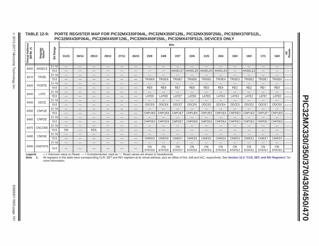
2012-2017 M
icrochip Technology Inc.D
S60001185G
-page
151
PIC32M
X330/350/370/430/450/470
TABLE 12-9: PORTE REGISTER MAP FOR PIC32MX330F064L, PIC32MX350F128L, PIC32MX350F256L, PIC32MX370F512L, PIC32MX430F064L, PIC32MX450F128L, PIC32MX450F256L, PIC32MX470F512L DEVICES ONLY
Virtu
al A
ddre
ss(B
F88_
#)
Reg
iste
rN
ame(1
)
Bit
Ran
ge
Bits
All
Res
ets
31/15 30/14 29/13 28/12 27/11 26/10 25/9 24/8 23/7 22/6 21/5 20/4 19/3 18/2 17/1 16/0
6400 ANSELE31:16 — — — — — — — — — — — — — — — — 000015:0 — — — — — — — — ANSELE7 ANSELE6 ANSELE5 ANSELE4 — ANSELE2 — — 00F4
6410 TRISE31:16 — — — — — — — — — — — — — — — — 000015:0 — — — — — — TRISE9 TRISE8 TRISE7 TRISE6 TRISE5 TRISE4 TRISE3 TRISE2 TRISE1 TRISE0 xxxx
6420 PORTE31:16 — — — — — — — — — — — — — — — — 000015:0 — — — — — — RE9 RE8 RE7 RE6 RE5 RE4 RE3 RE2 RE1 RE0 xxxx
6440 LATE31:16 — — — — — — — — — — — — — — — — 000015:0 — — — — — — LATE9 LATE8 LATE7 LATE6 LATE5 LATE4 LATE3 LATE2 LATE1 LATE0 xxxx
6440 ODCE31:16 — — — — — — — — — — — — — — — — 0000
15:0 — — — — — — ODCE9 ODCE8 ODCE7 ODCE6 ODCE5 ODCE4 ODCE3 ODCE2 ODCE1 ODCE0 xxxx
6450 CNPUE31:16 — — — — — — — — — — — — — — — — 000015:0 — — — — — — CNPUE9 CNPUE8 CNPUE7 CNPUE6 CNPUE5 CNPUE4 CNPDE3 CNPUE2 CNPUE1 CNPUE0 xxxx
6460 CNPDE31:16 — — — — — — — — — — — — — — — — 000015:0 — — — — — — CNPDE9 CNPDE8 CNPDE7 CNPDE6 CNPDE5 CNPDE4 CNPDE3 CNPDE2 CNPDE1 CNPDE0 xxxx
6470 CNCONE31:16 — — — — — — — — — — — — — — — — 000015:0 ON — SIDL — — — — — — — — — — — — — 0000
6480 CNENE31:16 — — — — — — — — — — — — — — — — 000015:0 — — — — — — CNIEE9 CNIEE8 CNIEE7 CNIEE6 CNIEE5 CNIEE4 CNIEE3 CNIEE2 CNIEE1 CNIEE0 xxxx
6490 CNSTATE31:16 — — — — — — — — — — — — — — — — 0000
15:0 — — — — — — CNSTATE9
CNSTATE8
CNSTATE7
CNSTATE6
CNSTATE5
CNSTATE4
CNSTATE3
CNSTATE2
CNSTATE1
CNSTATE0 xxxx
Legend: x = Unknown value on Reset; — = Unimplemented, read as ‘0’; Reset values are shown in hexadecimal.Note 1: All registers in this table have corresponding CLR, SET and INV registers at its virtual address, plus an offset of 0x4, 0x8 and 0xC, respectively. See Section 12.2 “CLR, SET, and INV Registers” for
more information.

PIC32M
X330/350/370/430/450/470
DS
60001185G-page
152
2012-2017 M
icrochip Technology Inc.
TABLE 12-10: PORTE REGISTER MAP FOR PIC32MX330F064H, PIC32MX350F128H, PIC32MX350F256H, PIC32MX370F512H, PIC32MX430F064H, PIC32MX450F128H, PIC32MX450F256H, AND PIC32MX470F512H DEVICES ONLY
Virtu
al A
ddre
ss(B
F88_
#)
Reg
iste
rN
ame(1
)
Bit
Ran
ge
Bits
All
Res
ets
31/15 30/14 29/13 28/12 27/11 26/10 25/9 24/8 23/7 22/6 21/5 20/4 19/3 18/2 17/1 16/0
6400 ANSELE31:16 — — — — — — — — — — — — — — — — 000015:0 — — — — — — — — ANSELE7 ANSELE6 ANSELE5 ANSELE4 — ANSELE2 — — 00F4
6410 TRISE31:16 — — — — — — — — — — — — — — — — 000015:0 — — — — — — — — TRISE7 TRISE6 TRISE5 TRISE4 TRISE3 TRISE2 TRISE1 TRISE0 xxxx
6420 PORTE31:16 — — — — — — — — — — — — — — — — 000015:0 — — — — — — — — RE7 RE6 RE5 RE4 RE3 RE2 RE1 RE0 xxxx
6440 LATE31:16 — — — — — — — — — — — — — — — — 000015:0 — — — — — — — — LATE7 LATE6 LATE5 LATE4 LATE3 LATE2 LATE1 LATE0 xxxx
6440 ODCE31:16 — — — — — — — — — — — — — — — — 000015:0 — — — — — — — — ODCE7 ODCE6 ODCE5 ODCE4 ODCE3 ODCE2 ODCE1 ODCE0 xxxx
6450 CNPUE31:16 — — — — — — — — — — — — — — — — 0000
15:0 — — — — — — — — CNPUE7 CNPUE6 CNPUE5 CNPUE4 CNPDE3 CNPUE2 CNPUE1 CNPUE0 xxxx
6460 CNPDE31:16 — — — — — — — — — — — — — — — — 000015:0 — — — — — — — — CNPDE7 CNPDE6 CNPDE5 CNPDE4 CNPDE3 CNPDE2 CNPDE1 CNPDE0 xxxx
6470 CNCONE31:16 — — — — — — — — — — — — — — — — 000015:0 ON — SIDL — — — — — — — — — — — — — 0000
6480 CNENE31:16 — — — — — — — — — — — — — — — — 000015:0 — — — — — — — — CNIEE7 CNIEE6 CNIEE5 CNIEE4 CNIEE3 CNIEE2 CNIEE1 CNIEE0 xxxx
6490 CNSTATE31:16 — — — — — — — — — — — — — — — — 0000
15:0 — — — — — — — — CNSTATE7
CNSTATE6
CNSTATE5
CNSTATE4
CNSTATE3
CNSTATE2
CNSTATE1
CNSTATE0 xxxx
Legend: x = Unknown value on Reset; — = Unimplemented, read as ‘0’; Reset values are shown in hexadecimal.Note 1: All registers in this table have corresponding CLR, SET and INV registers at its virtual address, plus an offset of 0x4, 0x8 and 0xC, respectively. See Section 12.2 “CLR, SET, and INV Registers” for
more information.

2012-2017 M
icrochip Technology Inc.D
S60001185G
-page
153
PIC32M
X330/350/370/430/450/470
TABLE 12-11: PORTF REGISTER MAP FOR PIC32MX330F064L, PIC32MX350F128L, PIC32MX350F256L, AND PIC32MX370F512L DEVICES ONLY
Virtu
al A
ddre
ss(B
F88_
#)
Reg
iste
rN
ame(1
)
Bit
Ran
ge
Bits
All
Res
ets
31/15 30/14 29/13 28/12 27/11 26/10 25/9 24/8 23/7 22/6 21/5 20/4 19/3 18/2 17/1 16/0
6510 TRISF31:16 — — — — — — — — — — — — — — — — 000015:0 — — TRISF13 TRISF12 — — — TRISF8 TRISF7 TRISF6 TRISF5 TRISF4 TRISF3 TRISF2 TRISF1 TRISF0 xxxx
6520 PORTF31:16 — — — — — — — — — — — — — — — — 000015:0 — — RF13 RF12 — — — RF8 RF7 RF6 RF5 RF4 RF3 RF2 RF1 RF0 xxxx
6530 LATF31:16 — — — — — — — — — — — — — — — — 000015:0 — — LATF13 LATF12 — — — LATF8 LATF7 LATF6 LATF5 LATF4 LATF3 LATF2 LATF1 LATF0 xxxx
6540 ODCF31:16 — — — — — — — — — — — — — — — — 000015:0 — — ODCF13 ODCF12 — — — ODCF8 ODCF7 ODCF6 ODCF5 ODCF4 ODCF3 ODCF2 ODCF1 ODCF0 xxxx
6550 CNPUF31:16 — — — — — — — — — — — — — — — — 0000
15:0 — — CNPUF13 CNPUF12 — — — CNPUF8 CNPUF7 CNPUF6 CNPUF5 CNPUF4 CNPDF3 CNPUF2 CNPUF1 CNPUF0 xxxx
6560 CNPDF31:16 — — — — — — — — — — — — — — — — 000015:0 — — CNPDF13 CNPDF12 — — — CNPDF8 CNPDF7 CNPDF6 CNPDF5 CNPDF4 CNPDF3 CNPDF2 CNPDF1 CNPDF0 xxxx
6570 CNCONF31:16 — — — — — — — — — — — — — — — — 000015:0 ON — SIDL — — — — — — — — — — — — — 0000
6580 CNENF31:16 — — — — — — — — — — — — — — — — 000015:0 — — CNIEF13 CNIEF12 — — — CNIEF8 CNIEF7 — CNIEF5 CNIEF4 CNIEF3 CNIEF2 CNIEF1 CNIEF0 xxxx
6590 CNSTATF31:16 — — — — — — — — — — — — — — — — 0000
15:0 — — CNSTATF13
CNSTATF12 — — — CN
STATF8CN
STATF7 — CNSTATF5
CNSTATF4
CNSTATF3
CNSTATF2
CNSTATF1
CNSTATF0 xxxx
Legend: x = Unknown value on Reset; — = Unimplemented, read as ‘0’; Reset values are shown in hexadecimal.Note 1: All registers in this table have corresponding CLR, SET and INV registers at its virtual address, plus an offset of 0x4, 0x8 and 0xC, respectively. See Section 12.2 “CLR, SET, and INV Registers” for
more information.

PIC32M
X330/350/370/430/450/470
DS
60001185G-page
154
2012-2017 M
icrochip Technology Inc.
TABLE 12-12: PORTF REGISTER MAP FOR PIC32MX430F064L, PIC32MX450F128L, PIC32MX450F256L, AND PIC32MX470F512L DEVICES ONLY
Virtu
al A
ddre
ss(B
F88_
#)
Reg
iste
rN
ame(1
)
Bit
Ran
ge
Bits
All
Res
ets
31/15 30/14 29/13 28/12 27/11 26/10 25/9 24/8 23/7 22/6 21/5 20/4 19/3 18/2 17/1 16/0
6510 TRISF31:16 — — — — — — — — — — — — — — — — 000015:0 — — TRISF13 TRISF12 — — — TRISF8 — — TRISF5 TRISF4 TRISF3 TRISF2 TRISF1 TRISF0 xxxx
6520 PORTF31:16 — — — — — — — — — — — — — — — — 000015:0 — — RF13 RF12 — — — RF8 — — RF5 RF4 RF3 RF2 RF1 RF0 xxxx
6530 LATF31:16 — — — — — — — — — — — — — — — — 000015:0 — — LATF13 LATF12 — — — LATF8 — — LATF5 LATF4 LATF3 LATF2 LATF1 LATF0 xxxx
6540 ODCF31:16 — — — — — — — — — — — — — — — — 000015:0 — — ODCF13 ODCF12 — — — ODCF8 — — ODCF5 ODCF4 ODCF3 ODCF2 ODCF1 ODCF0 xxxx
6550 CNPUF31:16 — — — — — — — — — — — — — — — — 000015:0 — — CNPUF13 CNPUF12 — — — CNPUF8 — — CNPUF5 CNPUF4 CNPDF3 CNPUF2 CNPUF1 CNPUF0 xxxx
6560 CNPDF31:16 — — — — — — — — — — — — — — — — 0000
15:0 — — CNPDF13 CNPDF12 — — — CNPDF8 — — CNPDF5 CNPFF4 CNPDF3 CNPDF2 CNPDF1 CNPDF0 xxxx
6570 CNCONF31:16 — — — — — — — — — — — — — — — — 000015:0 ON — SIDL — — — — — — — — — — — — — 0000
6580 CNENF31:16 — — — — — — — — — — — — — — — — 000015:0 — — CNIEF13 CNIEF12 — — — CNIEF8 — — CNIEF5 CNIEF4 CNIEF3 CNIEF2 CNIEF1 CNIEF0 xxxx
6590 CNSTATF31:16 — — — — — — — — — — — — — — — — 0000
15:0 — — CNSTATF13
CNSTATF12 — — — CN
STATF8 — — CNSTATF5
CNSTATF4
CNSTATF3
CNSTATF2
CNSTATF1
CNSTATF0 xxxx
Legend: x = Unknown value on Reset; — = Unimplemented, read as ‘0’; Reset values are shown in hexadecimal.Note 1: All registers in this table have corresponding CLR, SET and INV registers at its virtual address, plus an offset of 0x4, 0x8 and 0xC, respectively. See Section 12.2 “CLR, SET, and INV Registers” for
more information.

2012-2017 M
icrochip Technology Inc.D
S60001185G
-page
155
PIC32M
X330/350/370/430/450/470
TABLE 12-13: PORTF REGISTER MAP FOR PIC32MX330F064H, PIC32MX350F128H, PIC32MX350F256H, AND PIC32MX370F512H DEVICES ONLY
Virtu
al A
ddre
ss(B
F88_
#)
Reg
iste
rN
ame(1
)
Bit
Ran
ge
Bits
All
Res
ets
31/15 30/14 29/13 28/12 27/11 26/10 25/9 24/8 23/7 22/6 21/5 20/4 19/3 18/2 17/1 16/0
6510 TRISF31:16 — — — — — — — — — — — — — — — — 000015:0 — — — — — — — — — TRISF6 TRISF5 TRISF4 TRISF3 TRISF2 TRISF1 TRISF0 xxxx
6520 PORTF31:16 — — — — — — — — — — — — — — — — 000015:0 — — — — — — — — — RF6 RF5 RF4 RF3 RF2 RF1 RF0 xxxx
6530 LATF31:16 — — — — — — — — — — — — — — — — 000015:0 — — — — — — — — — LATF6 LATF5 LATF4 LATF3 LATF2 LATF1 LATF0 xxxx
6540 ODCF31:16 — — — — — — — — — — — — — — — — 000015:0 — — — — — — — — — ODCF6 ODCF5 ODCF4 ODCF3 ODCF2 ODCF1 ODCF0 xxxx
6550 CNPUF31:16 — — — — — — — — — — — — — — — — 0000
15:0 — — — — — — — — — CNPUF6 CNPUF5 CNPUF4 CNPUF3 CNPUF2 CNPUF1 CNPUF0 xxxx
6560 CNPDF31:16 — — — — — — — — — — — — — — — — 000015:0 — — — — — — — — — CNPDF6 CNPDF5 CNPDF4 CNPDF3 CNPDF2 CNPDF1 CNPDF0 xxxx
6570 CNCONF31:16 — — — — — — — — — — — — — — — — 000015:0 ON — SIDL — — — — — — — — — — — — — 0000
6580 CNENF31:16 — — — — — — — — — — — — — — — — 000015:0 — — — — — — — — — — CNIEF5 CNIEF4 CNIEF3 CNIEF2 CNIEF1 CNIEF0 xxxx
6590 CNSTATF31:16 — — — — — — — — — — — — — — — — 0000
15:0 — — — — — — — — — — CNSTATF5
CNSTATF4
CNSTATF3
CNSTATF2
CNSTATF1
CNSTATF0 xxxx
Legend: x = Unknown value on Reset; — = Unimplemented, read as ‘0’; Reset values are shown in hexadecimal.Note 1: All registers in this table have corresponding CLR, SET and INV registers at its virtual address, plus an offset of 0x4, 0x8 and 0xC, respectively. See Section 12.2 “CLR, SET, and INV Registers” for
more information.

PIC32M
X330/350/370/430/450/470
DS
60001185G-page
156
2012-2017 M
icrochip Technology Inc.
TABLE 12-14: PORTF REGISTER MAP FOR PIC32MX430F064H, PIC32MX450F128H, PIC32MX450F256H, AND PIC32MX470F512H DEVICES ONLY
Virtu
al A
ddre
ss(B
F88_
#)
Reg
iste
rN
ame(1
)
Bit
Ran
ge
Bits
All
Res
ets
31/15 30/14 29/13 28/12 27/11 26/10 25/9 24/8 23/7 22/6 21/5 20/4 19/3 18/2 17/1 16/0
6510 TRISF31:16 — — — — — — — — — — — — — — — — 000015:0 — — — — — — — — — — TRISF5 TRISF4 TRISF3 — TRISF1 TRISF0 xxxx
6520 PORTF31:16 — — — — — — — — — — — — — — — — 000015:0 — — — — — — — — — — RF5 RF4 RF3 — RF1 RF0 xxxx
6530 LATF31:16 — — — — — — — — — — — — — — — — 000015:0 — — — — — — — — — — LATF5 LATF4 LATF3 — LATF1 LATF0 xxxx
6540 ODCF31:16 — — — — — — — — — — — — — — — — 000015:0 — — — — — — — — — — ODCF5 ODCF4 ODCF3 — ODCF1 ODCF0 xxxx
6550 CNPUF31:16 — — — — — — — — — — — — — — — — 000015:0 — — — — — — — — — — CNPUF5 CNPUF4 CNPUF3 — CNPUF1 CNPUF0 xxxx
6560 CNPDF31:16 — — — — — — — — — — — — — — — — 0000
15:0 — — — — — — — — — — CNPDF5 CNPDF4 CNPDF3 — CNPDF1 CNPDF0 xxxx
6570 CNCONF31:16 — — — — — — — — — — — — — — — — 000015:0 ON — SIDL — — — — — — — — — — — — — 0000
6580 CNENF31:16 — — — — — — — — — — — — — — — — 000015:0 — — — — — — — — — — CNIEF5 CNIEF4 CNIEF3 — CNIEF1 CNIEF0 xxxx
6590 CNSTATF31:16 — — — — — — — — — — — — — — — — 0000
15:0 — — — — — — — — — — CNSTATF5
CNSTATF4
CNSTATF3 — CN
STATF1CN
STATF0 xxxx
Legend: x = Unknown value on Reset; — = Unimplemented, read as ‘0’; Reset values are shown in hexadecimal.Note 1: All registers in this table have corresponding CLR, SET and INV registers at its virtual address, plus an offset of 0x4, 0x8 and 0xC, respectively. See Section 12.2 “CLR, SET, and INV Registers” for
more information.

2012-2017 M
icrochip Technology Inc.D
S60001185G
-page
157
PIC32M
X330/350/370/430/450/470
TABLE 12-15: PORTG REGISTER MAP FOR PIC32MX330F064L, PIC32MX350F128L, PIC32MX350F256L, PIC32MX370F512L, PIC32MX430F064L, PIC32MX450F128L, PIC32MX450F256L, AND PIC32MX470F512L DEVICES ONLY
Virtu
al A
ddre
ss(B
F88_
#)
Reg
iste
rN
ame(1
)
Bit
Ran
ge
Bits
All
Res
ets
31/15 30/14 29/13 28/12 27/11 26/10 25/9 24/8 23/7 22/6 21/5 20/4 19/3 18/2 17/1 16/0
6600 ANSELG31:16 — — — — — — — — — — — — — — — — 000015:0 — — — — — — ANSELG9 ANSELG8 ANSELG7 ANSELG6 — — — — — — 01C0
6610 TRISG31:16 — — — — — — — — — — — — — — — — 000015:0 TRISG15 TRISG14 TRISG13 TRISG12 — — TRISG9 TRISG8 TRISG7 TRISG6 — — TRISG3 TRISG2 TRISG1 TRISG0 xxxx
6620 PORTG31:16 — — — — — — — — — — — — — — — — 000015:0 RG15 RG14 RG13 RG12 — — RG9 RG8 RG7 RG6 — — RG3(2) RG2(2) RG1 RG0 xxxx
6630 LATG31:16 — — — — — — — — — — — — — — — — 000015:0 LATG15 LATG14 LATG13 LATG12 — — LATG9 LATG8 LATG7 LATG6 — — LATG3 LATG2 LATG1 LATG0 xxxx
6640 ODCG31:16 — — — — — — — — — — — — — — — — 000015:0 ODCG15 ODCG14 ODCG13 ODCG12 — — ODCG9 ODCG8 ODCG7 ODCG6 — — ODCG3 ODCG2 ODCG1 ODCG0 xxxx
6650 CNPUG31:16 — — — — — — — — — — — — — — — — 000015:0 CNPUG15 CNPUG14 CNPUG13 CNPUG12 — — CNPUG9 CNPUG8 CNPUG7 CNPUG6 — — CNPUG3 CNPUG2 CNPUG1 CNPUG0 xxxx
6660 CNPDG31:16 — — — — — — — — — — — — — — — — 000015:0 CNPDG15 CNPDG14 CNPDG13 CNPDG12 — — CNPDG9 CNPDG8 CNPDG7 CNPDG6 — — CNPDG3 CNPDG2 CNPDG1 CNPDG0 xxxx
6670 CNCONG31:16 — — — — — — — — — — — — — — — — 000015:0 ON — SIDL — — — — — — — — — — — — — 0000
6680 CNENG31:16 — — — — — — — — — — — — — — — — 000015:0 CNIEG15 CNIEG14 CNIEG13 CNIEG12 — — CNIEG9 CNIEG8 CNIEG7 CNIEG6 — — CNIEG3 CNIEG2 CNIEG1 CNIEG0 xxxx
6690 CNSTATG31:16 — — — — — — — — — — — — — — — — 0000
15:0 CNSTATG15
CNSTATG14
CNSTATG13
CNSTATG12 — — CN
STATG9CN
STATG8CN
STATG7CN
STATG6 — — CNSTATG3
CNSTATG2
CNSTATG1
CNSTATG0 xxxx
Legend: x = Unknown value on Reset; — = Unimplemented, read as ‘0’; Reset values are shown in hexadecimal.Note 1: All registers in this table have corresponding CLR, SET and INV registers at its virtual address, plus an offset of 0x4, 0x8 and 0xC, respectively. See Section 12.2 “CLR, SET, and INV Registers” for
more information.2: This bit only implemented on devices without a USB module.
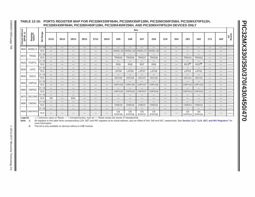
PIC32M
X330/350/370/430/450/470
DS
60001185G-page
158
2012-2017 M
icrochip Technology Inc.
TABLE 12-16: PORTG REGISTER MAP FOR PIC32MX330F064H, PIC32MX350F128H, PIC32MX350F256H, PIC32MX370F512H, PIC32MX430F064H, PIC32MX450F128H, PIC32MX450F256H, AND PIC32MX470F512H DEVICES ONLY
Virtu
al A
ddre
ss(B
F88_
#)
Reg
iste
rN
ame(1
)
Bit
Ran
ge
Bits
All
Res
ets
31/15 30/14 29/13 28/12 27/11 26/10 25/9 24/8 23/7 22/6 21/5 20/4 19/3 18/2 17/1 16/0
6600 ANSELG31:16 — — — — — — — — — — — — — — — — 000015:0 — — — — — — ANSELG9 ANSELG8 ANSELG7 ANSELG6 — — — — — — 01C0
6610 TRISG31:16 — — — — — — — — — — — — — — — — 000015:0 — — — — — — TRISG9 TRISG8 TRISG7 TRISG6 — — TRISG3 TRISG2 — — xxxx
6620 PORTG31:16 — — — — — — — — — — — — — — — — 000015:0 — — — — — — RG9 RG8 RG7 RG6 — — RG3(2) RG2(2) — — xxxx
6630 LATG31:16 — — — — — — — — — — — — — — — — 000015:0 — — — — — — LATG9 LATG8 LATG7 LATG6 — — LATG3 LATG2 — — xxxx
6640 ODCG31:16 — — — — — — — — — — — — — — — — 000015:0 — — — — — — ODCG9 ODCG8 ODCG7 ODCG6 — — ODCG3 ODCG2 — — xxxx
6650 CNPUG31:16 — — — — — — — — — — — — — — — — 0000
15:0 — — — — — — CNPUG9 CNPUG8 CNPUG7 CNPUG6 — — CNPUG3 CNPUG2 — — xxxx
6660 CNPDG31:16 — — — — — — — — — — — — — — — — 000015:0 — — — — — — CNPDG9 CNPDG8 CNPDG7 CNPDG6 — — CNPDG3 CNPDG2 — — xxxx
6670 CNCONG31:16 — — — — — — — — — — — — — — — — 000015:0 ON — SIDL — — — — — — — — — — — — — 0000
6680 CNENG31:16 — — — — — — — — — — — — — — — — 000015:0 — — — — — — CNIEG9 CNIEG8 CNIEG7 CNIEG6 — — CNIEG3 CNIEG2 — — xxxx
6690 CNSTATG31:16 — — — — — — — — — — — — — — — — 0000
15:0 — — — — — — CNSTATG9
CNSTATG8
CNSTATG7
CNSTATG6 — — CN
STATG3CN
STATG2 — — xxxx
Legend: x = Unknown value on Reset; — = Unimplemented, read as ‘0’; Reset values are shown in hexadecimal.Note 1: All registers in this table have corresponding CLR, SET and INV registers at its virtual address, plus an offset of 0x4, 0x8 and 0xC, respectively. See Section 12.2 “CLR, SET, and INV Registers” for
more information.2: This bit is only available on devices without a USB module.

2012-2017 M
icrochip Technology Inc.D
S60001185G
-page
159
PIC32M
X330/350/370/430/450/470
TABLE 12-17: PERIPHERAL PIN SELECT INPUT REGISTER MAP
Virt
ual A
ddre
ss(B
F80_
#)
Reg
iste
rN
ame
Bit
Ran
ge
Bits
All
Res
ets
31/15 30/14 29/13 28/12 27/11 26/10 25/9 24/8 23/7 22/6 21/5 20/4 19/3 18/2 17/1 16/0
FA04 INT1R31:16 — — — — — — — — — — — — — — — — 0000
15:0 — — — — — — — — — — — — INT1R<3:0> 0000
FA08 INT2R31:16 — — — — — — — — — — — — — — — — 0000
15:0 — — — — — — — — — — — — INT2R<3:0> 0000
FA0C INT3R31:16 — — — — — — — — — — — — — — — — 0000
15:0 — — — — — — — — — — — — INT3R<3:0> 0000
FA10 INT4R31:16 — — — — — — — — — — — — — — — — 0000
15:0 — — — — — — — — — — — — INT4R<3:0> 0000
FA18 T2CKR31:16 — — — — — — — — — — — — — — — — 0000
15:0 — — — — — — — — — — — — T2CKR<3:0> 0000
FA1C T3CKR31:16 — — — — — — — — — — — — — — — — 0000
15:0 — — — — — — — — — — — — T3CKR<3:0> 0000
FA20 T4CKR31:16 — — — — — — — — — — — — — — — — 0000
15:0 — — — — — — — — — — — — T4CKR<3:0> 0000
FA24 T5CKR31:16 — — — — — — — — — — — — — — — — 0000
15:0 — — — — — — — — — — — — T5CKR<3:0> 0000
FA28 IC1R31:16 — — — — — — — — — — — — — — — — 0000
15:0 — — — — — — — — — — — — IC1R<3:0> 0000
FA2C IC2R31:16 — — — — — — — — — — — — — — — — 0000
15:0 — — — — — — — — — — — — IC2R<3:0> 0000
FA30 IC3R31:16 — — — — — — — — — — — — — — — — 0000
15:0 — — — — — — — — — — — — IC3R<3:0> 0000
FA34 IC4R31:16 — — — — — — — — — — — — — — — — 0000
15:0 — — — — — — — — — — — — IC4R<3:0> 0000
FA38 IC5R31:16 — — — — — — — — — — — — — — — — 0000
15:0 — — — — — — — — — — — — IC5R<3:0> 0000
FA48 OCFAR31:16 — — — — — — — — — — — — — — — — 0000
15:0 — — — — — — — — — — — — OCFAR<3:0> 0000
FA50 U1RXR31:16 — — — — — — — — — — — — — — — — 0000
15:0 — — — — — — — — — — — — U1RXR<3:0> 0000
Legend: x = unknown value on Reset; — = unimplemented, read as ‘0’. Reset values are shown in hexadecimal.Note 1: This register is not available on 64-pin devices.

PIC32M
X330/350/370/430/450/470
DS
60001185G-page
160
2012-2017 M
icrochip Technology Inc.
FA54 U1CTSR31:16 — — — — — — — — — — — — — — — — 0000
15:0 — — — — — — — — — — — — U1CTSR<3:0> 0000
FA58 U2RXR31:16 — — — — — — — — — — — — — — — — 0000
15:0 — — — — — — — — — — — — U2RXR<3:0> 0000
FA5C U2CTSR31:16 — — — — — — — — — — — — — — — — 0000
15:0 — — — — — — — — — — — — U2CTSR<3:0> 0000
FA60 U3RXR31:16 — — — — — — — — — — — — — — — — 0000
15:0 — — — — — — — — — — — — U3RXR<3:0> 0000
FA64 U3CTSR31:16 — — — — — — — — — — — — — — — — 0000
15:0 — — — — — — — — — — — — U3CTSR<3:0> 0000
FA68 U4RXR31:16 — — — — — — — — — — — — — — — — 0000
15:0 — — — — — — — — — — — — U4RXR<3:0> 0000
FA6C U4CTSR31:16 — — — — — — — — — — — — — — — — 0000
15:0 — — — — — — — — — — — — U4CTSR<3:0> 0000
FA70 U5RXR(1) 31:16 — — — — — — — — — — — — — — — — 0000
15:0 — — — — — — — — — — — — U5RXR<3:0> 0000
FA74 U5CTSR(1) 31:16 — — — — — — — — — — — — — — — — 0000
15:0 — — — — — — — — — — — — U5CTSR<3:0> 0000
FA84 SDI1R31:16 — — — — — — — — — — — — — — — — 0000
15:0 — — — — — — — — — — — — SDI1R<3:0> 0000
FA88 SS1R31:16 — — — — — — — — — — — — — — — — 0000
15:0 — — — — — — — — — — — — SS1R<3:0> 0000
FA90 SDI2R31:16 — — — — — — — — — — — — — — — — 0000
15:0 — — — — — — — — — — — — SDI2R<3:0> 0000
FA94 SS2R31:16 — — — — — — — — — — — — — — — — 0000
15:0 — — — — — — — — — — — — SS2R<3:0> 0000
FAD0 REFCLKIR31:16 — — — — — — — — — — — — — — — — 0000
15:0 — — — — — — — — — — — — REFCLKIR<3:0> 0000
TABLE 12-17: PERIPHERAL PIN SELECT INPUT REGISTER MAP (CONTINUED)Vi
rtua
l Add
ress
(BF8
0_#)
Reg
iste
rN
ame
Bit
Ran
ge
Bits
All
Res
ets
31/15 30/14 29/13 28/12 27/11 26/10 25/9 24/8 23/7 22/6 21/5 20/4 19/3 18/2 17/1 16/0
Legend: x = unknown value on Reset; — = unimplemented, read as ‘0’. Reset values are shown in hexadecimal.Note 1: This register is not available on 64-pin devices.

2012-2017 M
icrochip Technology Inc.D
S60001185G
-page
161
PIC32M
X330/350/370/430/450/470
TABLE 12-18: PERIPHERAL PIN SELECT OUTPUT REGISTER MAP
Virt
ual A
ddre
ss(B
F80_
#)
Reg
iste
rN
ame
Bit
Ran
ge
Bits
All
Res
ets
31/15 30/14 29/13 28/12 27/11 26/10 25/9 24/8 23/7 22/6 21/5 20/4 19/3 18/2 17/1 16/0
FB38 RPA14R(1) 31:16 — — — — — — — — — — — — — — — — 000015:0 — — — — — — — — — — — — RPA14<3:0> 0000
FB3C RPA15R(1) 31:16 — — — — — — — — — — — — — — — — 000015:0 — — — — — — — — — — — — RPA15<3:0> 0000
FB40 RPB0R31:16 — — — — — — — — — — — — — — — — 000015:0 — — — — — — — — — — — — RPB0<3:0> 0000
FB44 RPB1R31:16 — — — — — — — — — — — — — — — — 000015:0 — — — — — — — — — — — — RPB1<3:0> 0000
FB48 RPB2R31:16 — — — — — — — — — — — — — — — — 000015:0 — — — — — — — — — — — — RPB2<3:0> 0000
FB4C RPB3R31:16 — — — — — — — — — — — — — — — — 000015:0 — — — — — — — — — — — — RPB3<3:0> 0000
FB54 RPB5R31:16 — — — — — — — — — — — — — — — — 000015:0 — — — — — — — — — — — — RPB5<3:0> 0000
FB58 RPB6R31:16 — — — — — — — — — — — — — — — — 000015:0 — — — — — — — — — — — — RPB6<3:0> 0000
FB5C RPB7R31:16 — — — — — — — — — — — — — — — — 000015:0 — — — — — — — — — — — — RPB7<3:0> 0000
FB60 RPB8R31:16 — — — — — — — — — — — — — — — — 000015:0 — — — — — — — — — — — — RPB8<3:0> 0000
FB64 RPB9R31:16 — — — — — — — — — — — — — — — — 000015:0 — — — — — — — — — — — — RPB9<3:0> 0000
FB68 RPB10R31:16 — — — — — — — — — — — — — — — — 000015:0 — — — — — — — — — — — — RPB10<3:0> 0000
FB78 RPB14R31:16 — — — — — — — — — — — — — — — — 000015:0 — — — — — — — — — — — — RPB14<3:0> 0000
FB7C RPB15R31:16 — — — — — — — — — — — — — — — — 000015:0 — — — — — — — — — — — — RPB15<3:0> 0000
FB84 RPC1R(1) 31:16 — — — — — — — — — — — — — — — — 000015:0 — — — — — — — — — — — — RPC1<3:0> 0000
FB88 RPC2R(1) 31:16 — — — — — — — — — — — — — — — — 000015:0 — — — — — — — — — — — — RPC2<3:0> 0000
FB8C RPC3R(1) 31:16 — — — — — — — — — — — — — — — — 000015:0 — — — — — — — — — — — — RPC3<3:0> 0000
Legend: x = unknown value on Reset; — = unimplemented, read as ‘0’. Reset values are shown in hexadecimal.Note 1: This register is not available on 64-pin devices.
2: This register is only available on devices without a USB module.3: This register is not available on 64-pin devices with a USB module.

PIC32M
X330/350/370/430/450/470
DS
60001185G-page
162
2012-2017 M
icrochip Technology Inc.
FB90 RPC4R(1) 31:16 — — — — — — — — — — — — — — — — 000015:0 — — — — — — — — — — — — RPC4<3:0> 0000
FBB4 RPC13R31:16 — — — — — — — — — — — — — — — — 000015:0 — — — — — — — — — — — — RPC13<3:0> 0000
FBB8 RPC14R31:16 — — — — — — — — — — — — — — — — 000015:0 — — — — — — — — — — — — RPC14<3:0> 0000
FBC0 RPD0R31:16 — — — — — — — — — — — — — — — — 000015:0 — — — — — — — — — — — — RPD0<3:0> 0000
FBC4 RPD1R31:16 — — — — — — — — — — — — — — — — 000015:0 — — — — — — — — — — — — RPD1<3:0> 0000
FBC8 RPD2R31:16 — — — — — — — — — — — — — — — — 000015:0 — — — — — — — — — — — — RPD2<3:0> 0000
FBCC RPD3R31:16 — — — — — — — — — — — — — — — — 000015:0 — — — — — — — — — — — — RPD3<3:0> 0000
FBD0 RPD4R31:16 — — — — — — — — — — — — — — — — 000015:0 — — — — — — — — — — — — RPD4<3:0> 0000
FBD4 RPD5R31:16 — — — — — — — — — — — — — — — — 000015:0 — — — — — — — — — — — — RPD5<3:0> 0000
FBE0 RPD8R31:16 — — — — — — — — — — — — — — — — 000015:0 — — — — — — — — — — — — RPD8<3:0> 0000
FBE4 RPD9R31:16 — — — — — — — — — — — — — — — — 000015:0 — — — — — — — — — — — — RPD9<3:0> 0000
FBE8 RPD10R31:16 — — — — — — — — — — — — — — — — 000015:0 — — — — — — — — — — — — RPD10<3:0> 0000
FBEC RPD11R31:16 — — — — — — — — — — — — — — — — 000015:0 — — — — — — — — — — — — RPD11<3:0> 0000
FBF0 RPD12R(1) 31:16 — — — — — — — — — — — — — — — — 000015:0 — — — — — — — — — — — — RPD12<3:0> 0000
FBF8 RPD14R(1) 31:16 — — — — — — — — — — — — — — — — 000015:0 — — — — — — — — — — — — RPD14<3:0> 0000
FBFC RPD15R(1) 31:16 — — — — — — — — — — — — — — — — 000015:0 — — — — — — — — — — — — RPD15<3:0> 0000
FC0C RPE3R31:16 — — — — — — — — — — — — — — — — 000015:0 — — — — — — — — — — — — RPE3<3:0> 0000
TABLE 12-18: PERIPHERAL PIN SELECT OUTPUT REGISTER MAP (CONTINUED)Vi
rtua
l Add
ress
(BF8
0_#)
Reg
iste
rN
ame
Bit
Ran
ge
Bits
All
Res
ets
31/15 30/14 29/13 28/12 27/11 26/10 25/9 24/8 23/7 22/6 21/5 20/4 19/3 18/2 17/1 16/0
Legend: x = unknown value on Reset; — = unimplemented, read as ‘0’. Reset values are shown in hexadecimal.Note 1: This register is not available on 64-pin devices.
2: This register is only available on devices without a USB module.3: This register is not available on 64-pin devices with a USB module.

2012-2017 M
icrochip Technology Inc.D
S60001185G
-page
163
PIC32M
X330/350/370/430/450/470
FC14 RPE5R31:16 — — — — — — — — — — — — — — — — 000015:0 — — — — — — — — — — — — RPE5<3:0> 0000
FC20 RPE8R(1) 31:16 — — — — — — — — — — — — — — — — 000015:0 — — — — — — — — — — — — RPE8<3:0> 0000
FC24 RPE9R(1) 31:16 — — — — — — — — — — — — — — — — 000015:0 — — — — — — — — — — — — RPE9<3:0> 0000
FC40 RPF0R31:16 — — — — — — — — — — — — — — — — 000015:0 — — — — — — — — — — — — RPF0<3:0> 0000
FC44 RPF1R31:16 — — — — — — — — — — — — — — — — 000015:0 — — — — — — — — — — — — RPF1<3:0> 0000
FC48 RPF2R(3) 31:16 — — — — — — — — — — — — — — — — 000015:0 — — — — — — — — — — — — RPF2<3:0> 0000
FC4C RPF3R(2) 31:16 — — — — — — — — — — — — — — — — 000015:0 — — — — — — — — — — — — RPF3<3:0> 0000
FC50 RPF4R31:16 — — — — — — — — — — — — — — — — 000015:0 — — — — — — — — — — — — RPF4<3:0> 0000
FC54 RPF5R31:16 — — — — — — — — — — — — — — — — 000015:0 — — — — — — — — — — — — RPF5<3:0> 0000
FC58 RPF6R(2) 31:16 — — — — — — — — — — — — — — — — 000015:0 — — — — — — — — — — — — RPF6<3:0> 0000
FC60 RPF8R(1) 31:16 — — — — — — — — — — — — — — — — 000015:0 — — — — — — — — — — — — RPF8<3:0> 0000
FC70 RPF12R(1) 31:16 — — — — — — — — — — — — — — — — 000015:0 — — — — — — — — — — — — RPF12<3:0> 0000
FC74 RPF13R(1) 31:16 — — — — — — — — — — — — — — — — 000015:0 — — — — — — — — — — — — RPF13<3:0> 0000
FC80 RPG0R(1) 31:16 — — — — — — — — — — — — — — — — 000015:0 — — — — — — — — — — — — RPG0<3:0> 0000
FC84 RPG1R(1) 31:16 — — — — — — — — — — — — — — — — 000015:0 — — — — — — — — — — — — RPG1<3:0> 0000
FC98 RPG6R31:16 — — — — — — — — — — — — — — — — 000015:0 — — — — — — — — — — — — RPG6<3:0> 0000
FC9C RPG7R31:16 — — — — — — — — — — — — — — — — 000015:0 — — — — — — — — — — — — RPG7<3:0> 0000
TABLE 12-18: PERIPHERAL PIN SELECT OUTPUT REGISTER MAP (CONTINUED)Vi
rtua
l Add
ress
(BF8
0_#)
Reg
iste
rN
ame
Bit
Ran
ge
Bits
All
Res
ets
31/15 30/14 29/13 28/12 27/11 26/10 25/9 24/8 23/7 22/6 21/5 20/4 19/3 18/2 17/1 16/0
Legend: x = unknown value on Reset; — = unimplemented, read as ‘0’. Reset values are shown in hexadecimal.Note 1: This register is not available on 64-pin devices.
2: This register is only available on devices without a USB module.3: This register is not available on 64-pin devices with a USB module.

PIC32M
X330/350/370/430/450/470
DS
60001185G-page
164
2012-2017 M
icrochip Technology Inc.
FCA0 RPG8R31:16 — — — — — — — — — — — — — — — — 000015:0 — — — — — — — — — — — — RPG8<3:0> 0000
FCA4 RPG9R31:16 — — — — — — — — — — — — — — — — 000015:0 — — — — — — — — — — — — RPG9<3:0> 0000
TABLE 12-18: PERIPHERAL PIN SELECT OUTPUT REGISTER MAP (CONTINUED)Vi
rtua
l Add
ress
(BF8
0_#)
Reg
iste
rN
ame
Bit
Ran
ge
Bits
All
Res
ets
31/15 30/14 29/13 28/12 27/11 26/10 25/9 24/8 23/7 22/6 21/5 20/4 19/3 18/2 17/1 16/0
Legend: x = unknown value on Reset; — = unimplemented, read as ‘0’. Reset values are shown in hexadecimal.Note 1: This register is not available on 64-pin devices.
2: This register is only available on devices without a USB module.3: This register is not available on 64-pin devices with a USB module.

2012-2017 Microchip Technology Inc. DS60001185G-page 165
PIC32MX330/350/370/430/450/470
REGISTER 12-1: [pin name]R: PERIPHERAL PIN SELECT INPUT REGISTER Bit
RangeBit
31/23/15/7Bit
30/22/14/6Bit
29/21/13/5Bit
28/20/12/4Bit
27/19/11/3Bit
26/18/10/2Bit
25/17/9/1Bit
24/16/8/0
31:24U-0 U-0 U-0 U-0 U-0 U-0 U-0 U-0
— — — — — — — —
23:16U-0 U-0 U-0 U-0 U-0 U-0 U-0 U-0
— — — — — — — —
15:8U-0 U-0 U-0 U-0 U-0 U-0 U-0 U-0
— — — — — — — —
7:0U-0 U-0 U-0 U-0 R/W-0 R/W-0 R/W-0 R/W-0
— — — — [pin name]R<3:0>
Legend:R = Readable bit W = Writable bit U = Unimplemented bit, read as ‘0’-n = Value at POR ‘1’ = Bit is set ‘0’ = Bit is cleared x = Bit is unknown
bit 31-4 Unimplemented: Read as ‘0’bit 3-0 [pin name]R<3:0>: Peripheral Pin Select Input bits
Where [pin name] refers to the pins that are used to configure peripheral input mapping. See Table 12-1 for input pin selection values.
Note: Register values can only be changed if the IOLOCK Configuration bit (CFGCON<13>) = 0.
REGISTER 12-2: RPnR: PERIPHERAL PIN SELECT OUTPUT REGISTER Bit
RangeBit
31/23/15/7Bit
30/22/14/6Bit
29/21/13/5Bit
28/20/12/4Bit
27/19/11/3Bit
26/18/10/2Bit
25/17/9/1Bit
24/16/8/0
31:24U-0 U-0 U-0 U-0 U-0 U-0 U-0 U-0
— — — — — — — —
23:16U-0 U-0 U-0 U-0 U-0 U-0 U-0 U-0
— — — — — — — —
15:8U-0 U-0 U-0 U-0 U-0 U-0 U-0 U-0
— — — — — — — —
7:0U-0 U-0 U-0 U-0 R/W-0 R/W-0 R/W-0 R/W-0
— — — — RPnR<3:0>
Legend:R = Readable bit W = Writable bit U = Unimplemented bit, read as ‘0’-n = Value at POR ‘1’ = Bit is set ‘0’ = Bit is cleared x = Bit is unknown
bit 31-4 Unimplemented: Read as ‘0’bit 3-0 RPnR<3:0>: Peripheral Pin Select Output bits
See Table 12-2 for output pin selection values.
Note: Register values can only be changed if the IOLOCK Configuration bit (CFGCON<13>) = 0.

PIC32MX330/350/370/430/450/470
DS60001185G-page 166 2012-2017 Microchip Technology Inc.
REGISTER 12-3: CNCONx: CHANGE NOTICE CONTROL FOR PORTx REGISTER (x = A – G) Bit
RangeBit
31/23/15/7Bit
30/22/14/6Bit
29/21/13/5Bit
28/20/12/4Bit
27/19/11/3Bit
26/18/10/2Bit
25/17/9/1Bit
24/16/8/0
31:24U-0 U-0 U-0 U-0 U-0 U-0 U-0 U-0
— — — — — — — —
23:16U-0 U-0 U-0 U-0 U-0 U-0 U-0 U-0
— — — — — — — —
15:8R/W-0 U-0 R/W-0 U-0 U-0 U-0 U-0 U-0
ON — SIDL — — — — —
7:0U-0 U-0 U-0 U-0 U-0 U-0 U-0 U-0
— — — — — — — —
Legend:R = Readable bit W = Writable bit U = Unimplemented bit, read as ‘0’-n = Value at POR ‘1’ = Bit is set ‘0’ = Bit is cleared x = Bit is unknown
bit 31-16 Unimplemented: Read as ‘0’bit 15 ON: Change Notice (CN) Control ON bit
1 = CN is enabled0 = CN is disabled
bit 14 Unimplemented: Read as ‘0’bit 13 SIDL: Stop in Idle Control bit
1 = CPU Idle Mode halts CN operation0 = CPU Idle does not affect CN operation
bit 12-0 Unimplemented: Read as ‘0’

2012-2017 Microchip Technology Inc. DS60001185G-page 167
PIC32MX330/350/370/430/450/47013.0 TIMER1
Note: This data sheet summarizes the features of the PIC32MX330/350/370/430/450/470 family of devices. It is not intended to be a comprehensive reference source. To complement the information in this data sheet, refer to Section 14. “Timers”(DS60001105), which is available from the Documentation > Reference Manual section of the Microchip PIC32 web site (www.microchip.com/pic32).
This family of PIC32 devices features one synchronous/asynchronous 16-bit timer that can operate as a free-running interval timer for various timing applications and counting external events. This timer can also be used with the Low-Power Secondary Oscillator (SOSC) for Real-Time Clock (RTC) applications.
The following modes are supported:
• Synchronous Internal Timer• Synchronous Internal Gated Timer• Synchronous External Timer• Asynchronous External Timer
13.1 Additional Supported Features• Selectable clock prescaler• Timer operation during CPU Idle and Sleep mode• Fast bit manipulation using CLR, SET and INV
registers• Asynchronous mode can be used with the SOSC
to function as a Real-Time Clock (RTC)
FIGURE 13-1: TIMER1 BLOCK DIAGRAM
ON
Sync
SOSCI
SOSCO/T1CK
TMR1
T1IF
Equal16-bit Comparator
PR1
Reset
SOSCEN
Event Flag
1
0
TSYNC
TGATE
TGATE
PBCLK
1
0
TCS
GateSync
TCKPS<1:0>
Prescaler
2
1, 8, 64, 256
x 1
1 0
0 0
Q
Q D
Note: The default state of the SOSCEN (OSCCON<1>) bit during a device Reset is controlled by the FSOSCEN bit in Configuration Word, DEVCFG1.
Data Bus<31:0>
<15:0>
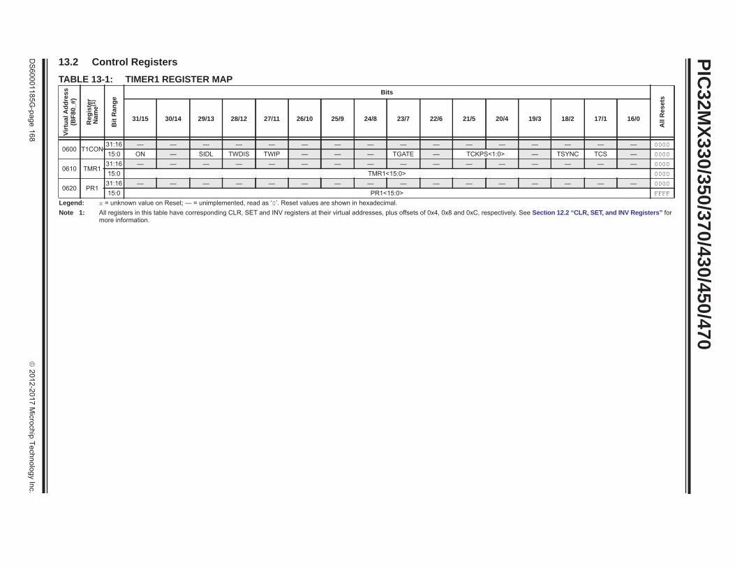
PIC32M
X330/350/370/430/450/470
DS
60001185G-page
168
2012-2017 M
icrochip Technology Inc.
13.2 Control RegistersTABLE 13-1: TIMER1 REGISTER MAP
Virt
ual A
ddre
ss(B
F80_
#)
Reg
iste
rN
ame(1
)
Bit
Ran
ge
Bits
All
Res
ets
31/15 30/14 29/13 28/12 27/11 26/10 25/9 24/8 23/7 22/6 21/5 20/4 19/3 18/2 17/1 16/0
0600 T1CON31:16 — — — — — — — — — — — — — — — — 000015:0 ON — SIDL TWDIS TWIP — — — TGATE — TCKPS<1:0> — TSYNC TCS — 0000
0610 TMR131:16 — — — — — — — — — — — — — — — — 000015:0 TMR1<15:0> 0000
0620 PR131:16 — — — — — — — — — — — — — — — — 000015:0 PR1<15:0> FFFF
Legend: x = unknown value on Reset; — = unimplemented, read as ‘0’. Reset values are shown in hexadecimal.Note 1: All registers in this table have corresponding CLR, SET and INV registers at their virtual addresses, plus offsets of 0x4, 0x8 and 0xC, respectively. See Section 12.2 “CLR, SET, and INV Registers” for
more information.

2012-2017 Microchip Technology Inc. DS60001185G-page 169
PIC32MX330/350/370/430/450/470
REGISTER 13-1: T1CON: TYPE A TIMER CONTROL REGISTER Bit
RangeBit
31/23/15/7Bit
30/22/14/6Bit
29/21/13/5Bit
28/20/12/4Bit
27/19/11/3Bit
26/18/10/2Bit
25/17/9/1Bit
24/16/8/0
31:24U-0 U-0 U-0 U-0 U-0 U-0 U-0 U-0
— — — — — — — —
23:16U-0 U-0 U-0 U-0 U-0 U-0 U-0 U-0
— — — — — — — —
15:8R/W-0 U-0 R/W-0 R/W-0 R-0 U-0 U-0 U-0
ON(1) — SIDL TWDIS TWIP — — —
7:0R/W-0 U-0 R/W-0 R/W-0 U-0 R/W-0 R/W-0 U-0
TGATE — TCKPS<1:0> — TSYNC TCS —
Legend:R = Readable bit W = Writable bit U = Unimplemented bit, read as ‘0’-n = Value at POR ‘1’ = Bit is set ‘0’ = Bit is cleared x = Bit is unknown
bit 31-16 Unimplemented: Read as ‘0’bit 15 ON: Timer On bit(1)
1 = Timer is enabled0 = Timer is disabled
bit 14 Unimplemented: Read as ‘0’bit 13 SIDL: Stop in Idle Mode bit
1 = Discontinue operation when device enters Idle mode0 = Continue operation even in Idle mode
bit 12 TWDIS: Asynchronous Timer Write Disable bit1 = Writes to TMR1 are ignored until pending write operation completes0 = Back-to-back writes are enabled (Legacy Asynchronous Timer functionality)
bit 11 TWIP: Asynchronous Timer Write in Progress bitIn Asynchronous Timer mode:1 = Asynchronous write to TMR1 register in progress0 = Asynchronous write to TMR1 register completeIn Synchronous Timer mode:This bit is read as ‘0’.
bit 10-8 Unimplemented: Read as ‘0’bit 7 TGATE: Timer Gated Time Accumulation Enable bit
When TCS = 1:This bit is ignored.When TCS = 0:1 = Gated time accumulation is enabled0 = Gated time accumulation is disabled
bit 6 Unimplemented: Read as ‘0’bit 5-4 TCKPS<1:0>: Timer Input Clock Prescale Select bits
11 = 1:256 prescale value10 = 1:64 prescale value01 = 1:8 prescale value00 = 1:1 prescale value
bit 3 Unimplemented: Read as ‘0’
Note 1: When using 1:1 PBCLK divisor, the user’s software should not read/write the peripheral SFRs in the SYSCLK cycle immediately following the instruction that clears the module’s ON bit.

PIC32MX330/350/370/430/450/470
DS60001185G-page 170 2012-2017 Microchip Technology Inc.
bit 2 TSYNC: Timer External Clock Input Synchronization Selection bitWhen TCS = 1:1 = External clock input is synchronized0 = External clock input is not synchronizedWhen TCS = 0:This bit is ignored.
bit 1 TCS: Timer Clock Source Select bit1 = External clock from TxCKI pin0 = Internal peripheral clock
bit 0 Unimplemented: Read as ‘0’
REGISTER 13-1: T1CON: TYPE A TIMER CONTROL REGISTER (CONTINUED)
Note 1: When using 1:1 PBCLK divisor, the user’s software should not read/write the peripheral SFRs in the SYSCLK cycle immediately following the instruction that clears the module’s ON bit.

2012-2017 Microchip Technology Inc. DS60001185G-page 171
PIC32MX330/350/370/430/450/47014.0 TIMER2/3, TIMER4/5
Note: This data sheet summarizes the features of the PIC32MX330/350/370/430/450/470 family of devices. It is not intended to be a comprehensive reference source. To complement the information in this data sheet, refer to Section 14. “Timers”(DS60001105), which is available from the Documentation > Reference Manual section of the Microchip PIC32 web site (www.microchip.com/pic32).
The PIC32MX330/350/370/430/450/470 family of devices features four synchronous 16-bit timers (default) that can operate as a free-running interval timer for various timing applications and counting external events. The following modes are supported:
• Synchronous internal 16-bit timer• Synchronous internal 16-bit gated timer• Synchronous external 16-bit timer
Two 32-bit synchronous timers are available by combining Timer2 with Timer3 and Timer4 with Timer5. The 32-bit timers can operate in three modes:
• Synchronous internal 32-bit timer• Synchronous internal 32-bit gated timer• Synchronous external 32-bit timer
Note: In this chapter, references to registers, TxCON, TMRx and PRx, use ‘x’ to represent Timer2 through 5 in 16-bit modes. In 32-bit modes, ‘x’ represents Timer2 or 4; ‘y’ represents Timer3 or 5.
14.1 Additional Supported Features• Selectable clock prescaler• Timers operational during CPU idle• Time base for Input Capture and Output Compare
modules (Timer2 and Timer3 only)• ADC event trigger (Timer3 in 16-bit mode, Timer2/
3 in 32-bit mode)• Fast bit manipulation using CLR, SET, and INV
registers
FIGURE 14-1: TIMER2, 3, 4, 5 BLOCK DIAGRAM (16-BIT)
Sync
PRx
TxIF
EqualComparator x 16
TMRxReset
Event Flag
Q
Q D
TGATE
1
0
Gate
TxCK
Sync
ON
TGATE
TCS
TCKPS
Prescaler
3
1, 2, 4, 8, 16,32, 64, 256
x 1
1 0
0 0PBCLK
Trigger(1)ADC Event
Note 1: ADC event trigger is available on Timer3 only.
Data Bus<31:0>
<15:0>

PIC32MX330/350/370/430/450/470
DS60001185G-page 172 2012-2017 Microchip Technology Inc.
FIGURE 14-2: TIMER2/3, 4/5 BLOCK DIAGRAM (32-BIT)(1)
TMRy(1) TMRx(1)
TyIF Event
Equal 32-bit Comparator
PRy PRx
Reset
LS Half WordMS Half Word
Flag
Note 1: In this diagram, the use of ‘x’ in registers, TxCON, TMRx, PRx and TxCK, refers to either Timer2 or Timer4; the use of ‘y’ in registers, TyCON, TMRy, PRy, TyIF, refers to either Timer3 or Timer5.
2: ADC event trigger is available only on the Timer2/3 pair.
TGATE
0
1
PBCLK
Gate
TxCK
Sync
Sync
ADC EventTrigger(2)
ON
TGATE
TCS
TCKPS
Prescaler
3
1, 2, 4, 8, 16,32, 64, 2561 0
0 0
Q
Q D
x 1
Data Bus<31:0>
<31:0>
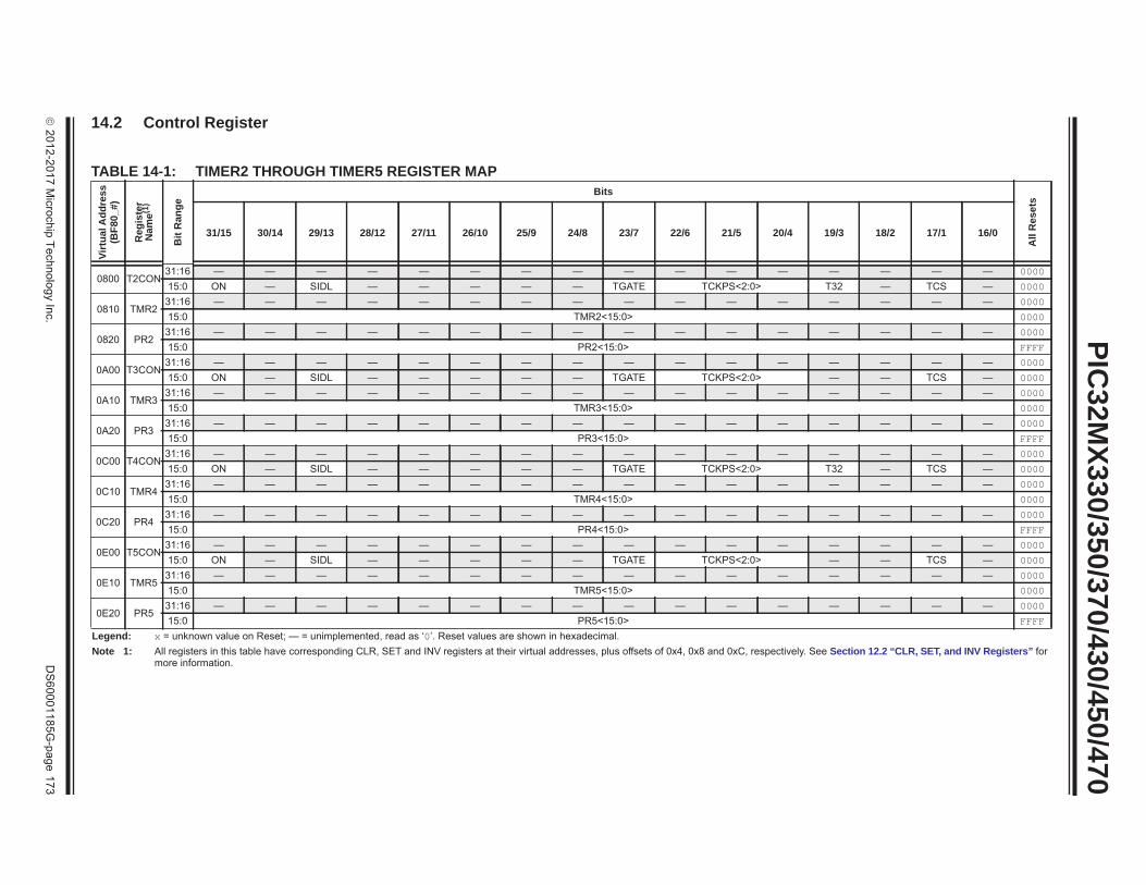
2012-2017 M
icrochip Technology Inc.D
S60001185G
-page
173
PIC32M
X330/350/370/430/450/470
14.2 Control Register
TABLE 14-1: TIMER2 THROUGH TIMER5 REGISTER MAP
Virt
ual A
ddre
ss(B
F80_
#)
Reg
iste
rN
ame(1
)
Bit
Ran
geBits
All
Res
ets
31/15 30/14 29/13 28/12 27/11 26/10 25/9 24/8 23/7 22/6 21/5 20/4 19/3 18/2 17/1 16/0
0800 T2CON31:16 — — — — — — — — — — — — — — — — 000015:0 ON — SIDL — — — — — TGATE TCKPS<2:0> T32 — TCS — 0000
0810 TMR231:16 — — — — — — — — — — — — — — — — 000015:0 TMR2<15:0> 0000
0820 PR231:16 — — — — — — — — — — — — — — — — 000015:0 PR2<15:0> FFFF
0A00 T3CON31:16 — — — — — — — — — — — — — — — — 000015:0 ON — SIDL — — — — — TGATE TCKPS<2:0> — — TCS — 0000
0A10 TMR331:16 — — — — — — — — — — — — — — — — 000015:0 TMR3<15:0> 0000
0A20 PR331:16 — — — — — — — — — — — — — — — — 000015:0 PR3<15:0> FFFF
0C00 T4CON31:16 — — — — — — — — — — — — — — — — 000015:0 ON — SIDL — — — — — TGATE TCKPS<2:0> T32 — TCS — 0000
0C10 TMR431:16 — — — — — — — — — — — — — — — — 000015:0 TMR4<15:0> 0000
0C20 PR431:16 — — — — — — — — — — — — — — — — 000015:0 PR4<15:0> FFFF
0E00 T5CON31:16 — — — — — — — — — — — — — — — — 000015:0 ON — SIDL — — — — — TGATE TCKPS<2:0> — — TCS — 0000
0E10 TMR531:16 — — — — — — — — — — — — — — — — 000015:0 TMR5<15:0> 0000
0E20 PR531:16 — — — — — — — — — — — — — — — — 000015:0 PR5<15:0> FFFF
Legend: x = unknown value on Reset; — = unimplemented, read as ‘0’. Reset values are shown in hexadecimal.Note 1: All registers in this table have corresponding CLR, SET and INV registers at their virtual addresses, plus offsets of 0x4, 0x8 and 0xC, respectively. See Section 12.2 “CLR, SET, and INV Registers” for
more information.

PIC32MX330/350/370/430/450/470
DS60001185G-page 174 2012-2017 Microchip Technology Inc.
REGISTER 14-1: TxCON: TYPE B TIMER CONTROL REGISTER Bit
RangeBit
31/23/15/7Bit
30/22/14/6Bit
29/21/13/5Bit
28/20/12/4Bit
27/19/11/3Bit
26/18/10/2Bit
25/17/9/1Bit
24/16/8/0
31:24U-0 U-0 U-0 U-0 U-0 U-0 U-0 U-0
— — — — — — — —
23:16U-0 U-0 U-0 U-0 U-0 U-0 U-0 U-0
— — — — — — — —
15:8R/W-0 U-0 R/W-0 U-0 U-0 U-0 U-0 U-0
ON(1,3) — SIDL(4) — — — — —
7:0R/W-0 R/W-0 R/W-0 R/W-0 R/W-0 U-0 R/W-0 U-0
TGATE(3) TCKPS<2:0>(3) T32(2) — TCS(3) —
Legend:R = Readable bit W = Writable bit U = Unimplemented bit, read as ‘0’
-n = Value at POR ‘1’ = Bit is set ‘0’ = Bit is cleared x = Bit is unknown
bit 31-16 Unimplemented: Read as ‘0’
bit 15 ON: Timer On bit(1,3)
1 = Module is enabled0 = Module is disabled
bit 14 Unimplemented: Read as ‘0’
bit 13 SIDL: Stop in Idle Mode bit(4)
1 = Discontinue operation when device enters Idle mode0 = Continue operation even in Idle mode
bit 12-8 Unimplemented: Read as ‘0’
bit 7 TGATE: Timer Gated Time Accumulation Enable bit(3)
When TCS = 1:This bit is ignored and is read as ‘0’.When TCS = 0:1 = Gated time accumulation is enabled0 = Gated time accumulation is disabled
bit 6-4 TCKPS<2:0>: Timer Input Clock Prescale Select bits(3)
111 = 1:256 prescale value110 = 1:64 prescale value101 = 1:32 prescale value100 = 1:16 prescale value011 = 1:8 prescale value010 = 1:4 prescale value001 = 1:2 prescale value000 = 1:1 prescale value
Note 1: When using 1:1 PBCLK divisor, the user’s software should not read/write the peripheral SFRs in the SYSCLK cycle immediately following the instruction that clears the module’s ON bit.
2: This bit is available only on even numbered timers (Timer2 and Timer4).3: While operating in 32-bit mode, this bit has no effect for odd numbered timers (Timer3 and Timer5). All
timer functions are set through the even numbered timers.4: While operating in 32-bit mode, this bit must be cleared on odd numbered timers to enable the 32-bit timer
in Idle mode.

2012-2017 Microchip Technology Inc. DS60001185G-page 175
PIC32MX330/350/370/430/450/470
bit 3 T32: 32-Bit Timer Mode Select bit(2)
1 = Odd numbered and even numbered timers form a 32-bit timer0 = Odd numbered and even numbered timers form a separate 16-bit timer
bit 2 Unimplemented: Read as ‘0’
bit 1 TCS: Timer Clock Source Select bit(3)
1 = External clock from TxCK pin0 = Internal peripheral clock
bit 0 Unimplemented: Read as ‘0’
REGISTER 14-1: TxCON: TYPE B TIMER CONTROL REGISTER (CONTINUED)
Note 1: When using 1:1 PBCLK divisor, the user’s software should not read/write the peripheral SFRs in the SYSCLK cycle immediately following the instruction that clears the module’s ON bit.
2: This bit is available only on even numbered timers (Timer2 and Timer4).3: While operating in 32-bit mode, this bit has no effect for odd numbered timers (Timer3 and Timer5). All
timer functions are set through the even numbered timers.4: While operating in 32-bit mode, this bit must be cleared on odd numbered timers to enable the 32-bit timer
in Idle mode.

PIC32MX330/350/370/430/450/470
DS60001185G-page 176 2012-2017 Microchip Technology Inc.
NOTES:

2012-2017 Microchip Technology Inc. DS60001185G-page 177
PIC32MX330/350/370/430/450/47015.0 WATCHDOG TIMER (WDT)
Note: This data sheet summarizes the features of the PIC32MX330/350/370/430/450/470 family of devices. It is not intended to be a comprehensive reference source. To complement the information in this data sheet, refer to Section 9. “Watchdog, Deadman, and Power-up Timers”(DS60001114), which is available from the Documentation > Reference Manual section of the Microchip PIC32 web site (www.microchip.com/pic32).
The WDT, when enabled, operates from the internal Low-Power Oscillator (LPRC) clock source and can be used to detect system software malfunctions by reset-ting the device if the WDT is not cleared periodically in software. Various WDT time-out periods can be selected using the WDT postscaler. The WDT can also be used to wake the device from Sleep or Idle mode.
The following are some of the key features of the WDT module:
• Configuration or software controlled• User-configurable time-out period• Can wake the device from Sleep or Idle
FIGURE 15-1: WATCHDOG AND POWER-UP TIMER BLOCK DIAGRAM
Wake
WDTCLR = 1WDT Enable
LPRC
Power Save
25-bit Counter
PWRT EnableWDT Enable
LPRC
WDT Counter Reset
Control
Oscillator
25Device Reset
NMI (Wake-up)
PWRT
PWRT Enable
FWDTPS<4:0> (DEVCFG1<20:16>)
Clock
Decoder
1
1:64 Output
01WDT Enable
Reset Event

PIC32M
X330/350/370/430/450/470
DS
60001185G-page
178
2012-2017 M
icrochip Technology Inc.
15.1 Watchdog Timer Control Registers
TABLE 15-1: WATCHDOG TIMER CONTROL REGISTER MAP
Virt
ual A
ddre
ss(B
F80_
#)
Reg
iste
rN
ame(1
)
Bit
Ran
ge
Bits
All
Res
ets
31/15 30/14 29/13 28/12 27/11 26/10 25/9 24/8 23/7 22/6 21/5 20/4 19/3 18/2 17/1 16/0
0000 WDTCON31:16 — — — — — — — — — — — — — — — — 000015:0 ON — — — — — — — — SWDTPS<4:0> WDTWINEN WDTCLR 0000
Legend: x = unknown value on Reset; — = unimplemented, read as ‘0’. Reset values are shown in hexadecimal.Note 1: All registers in this table have corresponding CLR, SET and INV registers at their virtual addresses, plus offsets of 0x4, 0x8 and 0xC, respectively. See Section 12.2 “CLR, SET, and INV Registers” for
more information.

2012-2017 Microchip Technology Inc. DS60001185G-page 179
PIC32MX330/350/370/430/450/470
REGISTER 15-1: WDTCON: WATCHDOG TIMER CONTROL REGISTERBit
RangeBit
31/23/15/7Bit
30/22/14/6Bit
29/21/13/5Bit
28/20/12/4Bit
27/19/11/3Bit
26/18/10/2Bit
25/17/9/1Bit
24/16/8/0
31:24U-0 U-0 U-0 U-0 U-0 U-0 U-0 U-0
— — — — — — — —
23:16U-0 U-0 U-0 U-0 U-0 U-0 U-0 U-0
— — — — — — — —
15:8R/W-0 U-0 U-0 U-0 U-0 U-0 U-0 U-0
ON(1,2) — — — — — — —
7:0U-0 R-y R-y R-y R-y R-y R/W-0 R/W-0
— SWDTPS<4:0> WDTWINEN WDTCLR
Legend: y = Values set from Configuration bits on PORR = Readable bit W = Writable bit U = Unimplemented bit, read as ‘0’-n = Value at POR ‘1’ = Bit is set ‘0’ = Bit is cleared x = Bit is unknown
bit 31-16 Unimplemented: Read as ‘0’bit 15 ON: Watchdog Timer Enable bit(1,2)
1 = Enables the WDT if it is not enabled by the device configuration0 = Disable the WDT if it was enabled in software
bit 14-7 Unimplemented: Read as ‘0’bit 6-2 SWDTPS<4:0>: Shadow Copy of Watchdog Timer Postscaler Value from Device Configuration bits
On reset, these bits are set to the values of the WDTPS <4:0> of Configuration bits.bit 1 WDTWINEN: Watchdog Timer Window Enable bit
1 = Enable windowed Watchdog Timer0 = Disable windowed Watchdog Timer
bit 0 WDTCLR: Watchdog Timer Reset bit1 = Writing a ‘1’ will clear the WDT0 = Software cannot force this bit to a ‘0’
Note 1: A read of this bit results in a ‘1’ if the Watchdog Timer is enabled by the device configuration or software.2: When using the 1:1 PBCLK divisor, the user software should not read or write the peripheral’s SFRs in the
SYSCLK cycle immediately following the instruction that clears the module’s ON bit.

PIC32MX330/350/370/430/450/470
DS60001185G-page 180 2012-2017 Microchip Technology Inc.
NOTES:
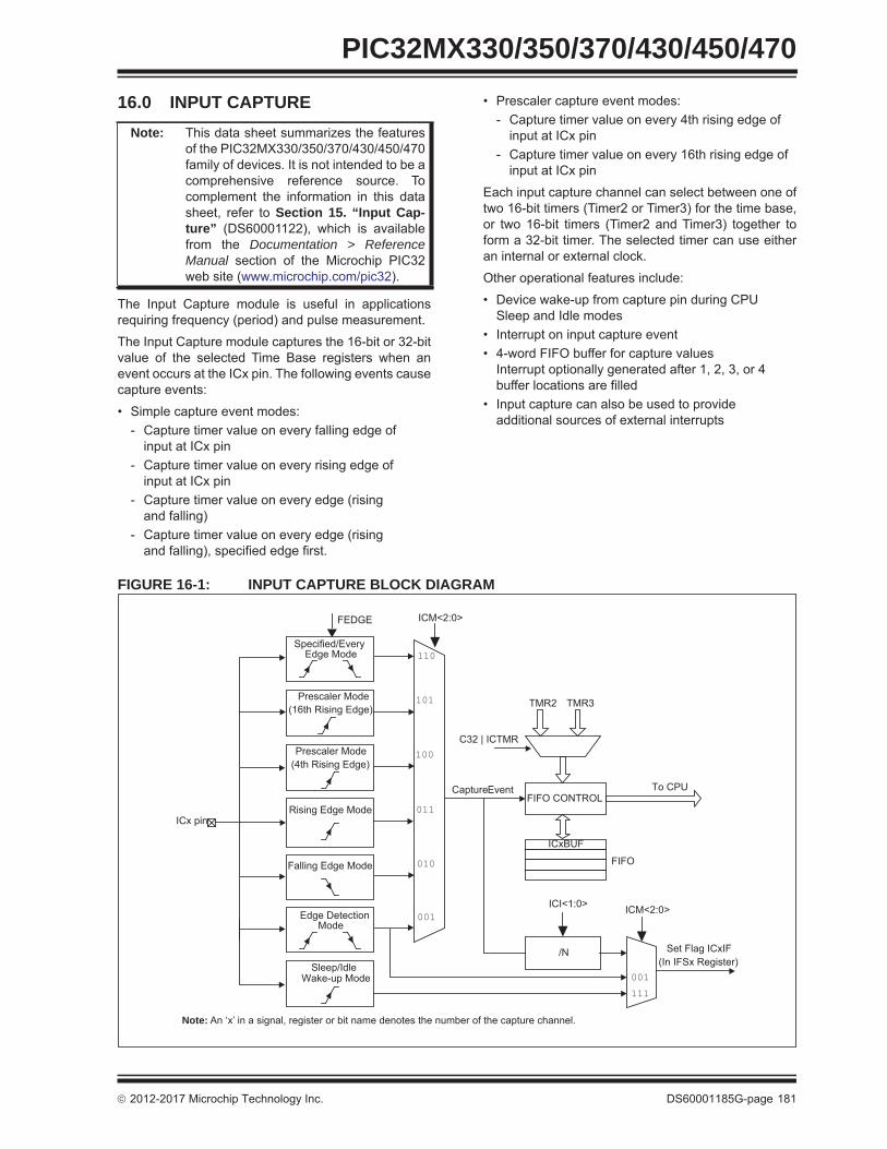
2012-2017 Microchip Technology Inc. DS60001185G-page 181
PIC32MX330/350/370/430/450/47016.0 INPUT CAPTURE
Note: This data sheet summarizes the features of the PIC32MX330/350/370/430/450/470 family of devices. It is not intended to be a comprehensive reference source. To complement the information in this data sheet, refer to Section 15. “Input Cap-ture” (DS60001122), which is available from the Documentation > Reference Manual section of the Microchip PIC32 web site (www.microchip.com/pic32).
The Input Capture module is useful in applications requiring frequency (period) and pulse measurement.
The Input Capture module captures the 16-bit or 32-bit value of the selected Time Base registers when an event occurs at the ICx pin. The following events cause capture events:
• Simple capture event modes:- Capture timer value on every falling edge of
input at ICx pin- Capture timer value on every rising edge of
input at ICx pin- Capture timer value on every edge (rising
and falling)- Capture timer value on every edge (rising
and falling), specified edge first.
• Prescaler capture event modes:- Capture timer value on every 4th rising edge of
input at ICx pin- Capture timer value on every 16th rising edge of
input at ICx pin
Each input capture channel can select between one of two 16-bit timers (Timer2 or Timer3) for the time base,or two 16-bit timers (Timer2 and Timer3) together to form a 32-bit timer. The selected timer can use either an internal or external clock.
Other operational features include:
• Device wake-up from capture pin during CPU Sleep and Idle modes
• Interrupt on input capture event• 4-word FIFO buffer for capture values
Interrupt optionally generated after 1, 2, 3, or 4 buffer locations are filled
• Input capture can also be used to provide additional sources of external interrupts
FIGURE 16-1: INPUT CAPTURE BLOCK DIAGRAM
Note: An ‘x’ in a signal, register or bit name denotes the number of the capture channel.
FIFO CONTROL
ICxBUF
TMR2 TMR3
CaptureEvent
/N
FIFO
ICI<1:0>
ICM<2:0>
ICM<2:0>
101
100
011
010
001
001
111
To CPU
Set Flag ICxIF(In IFSx Register)
Rising Edge Mode
Prescaler Mode (4th Rising Edge)
Falling Edge Mode
Edge Detection
Prescaler Mode (16th Rising Edge)
Sleep/IdleWake-up Mode
C32 | ICTMR
ICx pin
Mode
110Specified/Every
Edge Mode
FEDGE

PIC32MX330/350/370/430/450/470
DS60001185G-page 182 2012-2017 Microchip Technology Inc.
16.1 Control RegisterREGISTER 16-1: ICXCON: INPUT CAPTURE ‘X’ CONTROL REGISTER
Bit Range Bit31/23/15/7
Bit30/22/14/6
Bit29/21/13/5
Bit28/20/12/4
Bit27/19/11/3
Bit26/18/10/2
Bit25/17/9/1
Bit24/16/8/0
31:24U-0 U-0 U-0 U-0 U-0 U-0 U-0 U-0
— — — — — — — —
23:16U-0 U-0 U-0 U-0 U-0 U-0 U-0 U-0
— — — — — — — —
15:8R/W-0 U-0 R/W-0 U-0 U-0 U-0 R/W-0 R/W-0
ON(1) — SIDL — — — FEDGE C32
7:0R/W-0 R/W-0 R/W-0 R-0 R-0 R/W-0 R/W-0 R/W-0
ICTMR ICI<1:0> ICOV ICBNE ICM<2:0>
Legend:R = Readable bit W = Writable bit U = Unimplemented bit-n = Bit Value at POR: (‘0’, ‘1’, x = unknown) P = Programmable bit r = Reserved bit
bit 31-16 Unimplemented: Read as ‘0’bit 15 ON: Input Capture Module Enable bit(1)
1 = Module is enabled0 = Disable and reset module, disable clocks, disable interrupt generation and allow SFR modifications
bit 14 Unimplemented: Read as ‘0’bit 13 SIDL: Stop in Idle Control bit
1 = Halt in CPU Idle mode0 = Continue to operate in CPU Idle mode
bit 12-10 Unimplemented: Read as ‘0’bit 9 FEDGE: First Capture Edge Select bit (only used in mode 6, ICM<2:0> = 110)
1 = Capture rising edge first0 = Capture falling edge first
bit 8 C32: 32-bit Capture Select bit1 = 32-bit timer resource capture0 = 16-bit timer resource capture
bit 7 ICTMR: Timer Select bit (Does not affect timer selection when C32 (ICxCON<8>) is ‘1’)0 = Timer3 is the counter source for capture1 = Timer2 is the counter source for capture
bit 6-5 ICI<1:0>: Interrupt Control bits11 = Interrupt on every fourth capture event10 = Interrupt on every third capture event01 = Interrupt on every second capture event00 = Interrupt on every capture event
bit 4 ICOV: Input Capture Overflow Status Flag bit (read-only)1 = Input capture overflow has occurred0 = No input capture overflow has occurred
bit 3 ICBNE: Input Capture Buffer Not Empty Status bit (read-only)1 = Input capture buffer is not empty; at least one more capture value can be read0 = Input capture buffer is empty
Note 1: When using 1:1 PBCLK divisor, the user software should not read/write the peripheral’s SFRs in the SYSCLK cycle immediately following the instruction that clears the module’s ON bit.

2012-2017 Microchip Technology Inc. DS60001185G-page 183
PIC32MX330/350/370/430/450/470
bit 2-0 ICM<2:0>: Input Capture Mode Select bits111 = Interrupt-Only mode (only supported while in Sleep mode or Idle mode)110 = Simple Capture Event mode – every edge, specified edge first and every edge thereafter101 = Prescaled Capture Event mode – every sixteenth rising edge100 = Prescaled Capture Event mode – every fourth rising edge011 = Simple Capture Event mode – every rising edge010 = Simple Capture Event mode – every falling edge001 = Edge Detect mode – every edge (rising and falling)000 = Input Capture module is disabled
REGISTER 16-1: ICXCON: INPUT CAPTURE ‘X’ CONTROL REGISTER (CONTINUED)
Note 1: When using 1:1 PBCLK divisor, the user software should not read/write the peripheral’s SFRs in the SYSCLK cycle immediately following the instruction that clears the module’s ON bit.

PIC32MX330/350/370/430/450/470
DS60001185G-page 184 2012-2017 Microchip Technology Inc.
NOTES:

2012-2017 Microchip Technology Inc. DS60001185G-page 185
PIC32MX330/350/370/430/450/47017.0 OUTPUT COMPARE
Note: This data sheet summarizes the features of the PIC32MX330/350/370/430/450/470 family of devices. It is not intended to be a comprehensive reference source. To complement the information in this data sheet, refer to Section 16. “Output Com-pare” (DS60001111), which is available from the Documentation > Reference Manual section of the Microchip PIC32 web site (www.microchip.com/pic32).
The Output Compare module is used to generate a single pulse or a train of pulses in response to selected time base events. For all modes of operation, the Output Compare module compares the values stored in the OCxR and/or the OCxRS registers to the value in the selected timer. When a match occurs, the Output Compare module generates an event based on the selected mode of operation.
The following are key features of the Output Compare module:
• Multiple Output Compare modules in a device• Programmable interrupt generation on compare
event• Single and Dual Compare modes• Single and continuous output pulse generation• Pulse-Width Modulation (PWM) mode• Hardware-based PWM Fault detection and
automatic output disable• Can operate from either of two available 16-bit
time bases or a single 32-bit time base
FIGURE 17-1: OUTPUT COMPARE MODULE BLOCK DIAGRAM
OCxR(1)
Comparator
OutputLogic
QSR
OCM<2:0>
Output Enable
OCx(1)
Set Flag bitOCxIF(1)
OCxRS(1)
Mode Select
3
Note 1: Where ‘x’ is shown, reference is made to the registers associated with the respective output compare channels, 1 through 5.
2: The OCFA pin controls the OC1-OC4 channels. The OCFB pin controls the OC5 channel.
0 1 OCTSEL 0 1
16 16
OCFA or OCFB(2)
Timer2 Timer2 Timer3
LogicOutput Enable
Timer3Rollover Rollover
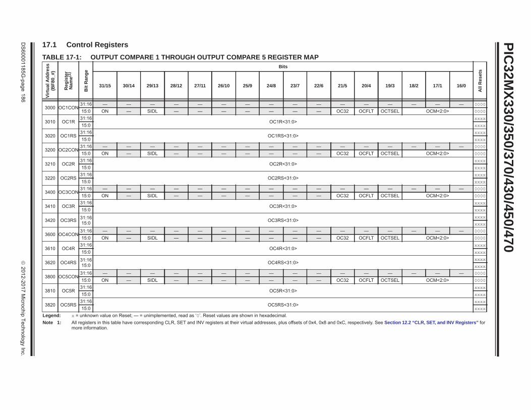
PIC32M
X330/350/370/430/450/470
DS
60001185G-page
186
2012-2017 M
icrochip Technology Inc.
17.1 Control RegistersTABLE 17-1: OUTPUT COMPARE 1 THROUGH OUTPUT COMPARE 5 REGISTER MAP
Virt
ual A
ddre
ss(B
F80_
#)
Reg
iste
rN
ame(1
)
Bit
Ran
ge
Bits
All
Res
ets
31/15 30/14 29/13 28/12 27/11 26/10 25/9 24/8 23/7 22/6 21/5 20/4 19/3 18/2 17/1 16/0
3000 OC1CON31:16 — — — — — — — — — — — — — — — — 000015:0 ON — SIDL — — — — — — — OC32 OCFLT OCTSEL OCM<2:0> 0000
3010 OC1R31:16
OC1R<31:0>xxxx
15:0 xxxx
3020 OC1RS31:16
OC1RS<31:0>xxxx
15:0 xxxx
3200 OC2CON31:16 — — — — — — — — — — — — — — — — 000015:0 ON — SIDL — — — — — — — OC32 OCFLT OCTSEL OCM<2:0> 0000
3210 OC2R31:16
OC2R<31:0>xxxx
15:0 xxxx
3220 OC2RS31:16
OC2RS<31:0>xxxx
15:0 xxxx
3400 OC3CON31:16 — — — — — — — — — — — — — — — — 000015:0 ON — SIDL — — — — — — — OC32 OCFLT OCTSEL OCM<2:0> 0000
3410 OC3R31:16
OC3R<31:0>xxxx
15:0 xxxx
3420 OC3RS 31:1615:0 OC3RS<31:0>
xxxxxxxx
3600 OC4CON31:16 — — — — — — — — — — — — — — — — 000015:0 ON — SIDL — — — — — — — OC32 OCFLT OCTSEL OCM<2:0> 0000
3610 OC4R31:16
OC4R<31:0>xxxx
15:0 xxxx
3620 OC4RS 31:1615:0 OC4RS<31:0>
xxxxxxxx
3800 OC5CON31:16 — — — — — — — — — — — — — — — — 000015:0 ON — SIDL — — — — — — — OC32 OCFLT OCTSEL OCM<2:0> 0000
3810 OC5R31:16
OC5R<31:0>xxxx
15:0 xxxx
3820 OC5RS31:16
OC5RS<31:0>xxxx
15:0 xxxxLegend: x = unknown value on Reset; — = unimplemented, read as ‘0’. Reset values are shown in hexadecimal.Note 1: All registers in this table have corresponding CLR, SET and INV registers at their virtual addresses, plus offsets of 0x4, 0x8 and 0xC, respectively. See Section 12.2 “CLR, SET, and INV Registers” for
more information.

2012-2017 Microchip Technology Inc. DS60001185G-page 187
PIC32MX330/350/370/430/450/470
REGISTER 17-1: OCxCON: OUTPUT COMPARE ‘x’ CONTROL REGISTER Bit
RangeBit
31/23/15/7Bit
30/22/14/6Bit
29/21/13/5Bit
28/20/12/4Bit
27/19/11/3Bit
26/18/10/2Bit
25/17/9/1Bit
24/16/8/0
31:24U-0 U-0 U-0 U-0 U-0 U-0 U-0 U-0
— — — — — — — —
23:16U-0 U-0 U-0 U-0 U-0 U-0 U-0 U-0
— — — — — — — —
15:8R/W-0 U-0 R/W-0 U-0 U-0 U-0 U-0 U-0
ON(1) — SIDL — — — — —
7:0U-0 U-0 R/W-0 R-0 R/W-0 R/W-0 R/W-0 R/W-0
— — OC32 OCFLT(2) OCTSEL OCM<2:0>
Legend:R = Readable bit W = Writable bit U = Unimplemented bit, read as ‘0’-n = Value at POR ‘1’ = Bit is set ‘0’ = Bit is cleared x = Bit is unknown
bit 31-16 Unimplemented: Read as ‘0’bit 15 ON: Output Compare Peripheral On bit(1)
1 = Output Compare peripheral is enabled0 = Output Compare peripheral is disabled
bit 14 Unimplemented: Read as ‘0’bit 13 SIDL: Stop in Idle Mode bit
1 = Discontinue operation when CPU enters Idle mode0 = Continue operation in Idle mode
bit 12-6 Unimplemented: Read as ‘0’bit 5 OC32: 32-bit Compare Mode bit
1 = OCxR<31:0> and/or OCxRS<31:0> are used for comparisions to the 32-bit timer source0 = OCxR<15:0> and OCxRS<15:0> are used for comparisons to the 16-bit timer source
bit 4 OCFLT: PWM Fault Condition Status bit(2)
1 = PWM Fault condition has occurred (cleared in HW only)0 = No PWM Fault condition has occurred
bit 3 OCTSEL: Output Compare Timer Select bit1 = Timer3 is the clock source for this Output Compare module0 = Timer2 is the clock source for this Output Compare module
bit 2-0 OCM<2:0>: Output Compare Mode Select bits111 = PWM mode on OCx; Fault pin is enabled110 = PWM mode on OCx; Fault pin is disabled101 = Initialize OCx pin low; generate continuous output pulses on OCx pin100 = Initialize OCx pin low; generate single output pulse on OCx pin011 = Compare event toggles OCx pin010 = Initialize OCx pin high; compare event forces OCx pin low001 = Initialize OCx pin low; compare event forces OCx pin high000 = Output compare peripheral is disabled but continues to draw current
Note 1: When using the 1:1 PBCLK divisor, the user software should not read/write the peripheral’s SFRs in the SYSCLK cycle immediately following the instruction that clears the module’s ON bit.
2: This bit is only used when OCM<2:0> = ‘111’. It is read as ‘0’ in all other modes.

PIC32MX330/350/370/430/450/470
DS60001185G-page 188 2012-2017 Microchip Technology Inc.
NOTES:

2012-2017 Microchip Technology Inc. DS60001185G-page 189
PIC32MX330/350/370/430/450/47018.0 SERIAL PERIPHERAL
INTERFACE (SPI)Note: This data sheet summarizes the features
of the PIC32MX330/350/370/430/450/470 family of devices. It is not intended to be a comprehensive reference source. To complement the information in this data sheet, refer to Section 23. “Serial Peripheral Interface (SPI)”(DS60001106), which is available from the Documentation > Reference Manual section of the Microchip PIC32 web site (www.microchip.com/pic32).
The SPI module is a synchronous serial interface that is useful for communicating with external peripherals and other microcontroller devices. These peripheral devices may be Serial EEPROMs, Shift registers, dis-play drivers, Analog-to-Digital Converters (ADC), etc. The PIC32 SPI module is compatible with Motorola®
SPI and SIOP interfaces.
The following are some of the key features of the SPI module:
• Master and Slave modes support• Four different clock formats• Enhanced Framed SPI protocol support• User-configurable 8-bit, 16-bit and 32-bit data width• Separate SPI FIFO buffers for receive and transmit
- FIFO buffers act as 4/8/16-level deep FIFOs based on 32/16/8-bit data width
• Programmable interrupt event on every 8-bit, 16-bit and 32-bit data transfer
• Operation during CPU Sleep and Idle mode• Audio Codec Support:
- I2S protocol- Left-justified- Right-justified- PCM
FIGURE 18-1: SPI MODULE BLOCK DIAGRAMInternal
Data Bus
SDIx
SDOx
SSx/FSYNC
SCKx
SPIxSRbit 0
ShiftControl
EdgeSelect
MSTEN
Baud Rate
Slave Select
Sync Control
ClockControl
Transmit
Receive
and Frame
Note: Access SPIxTXB and SPIxRXB FIFOs via SPIxBUF register.
FIFOs Share Address SPIxBUF
SPIxBUF
GeneratorPBCLK
WriteRead
SPIxTXB FIFOSPIxRXB FIFO
REFCLK
MCLKSEL
1
0

PIC32M
X330/350/370/430/450/470
DS
60001185G-page
190
2012-2017 M
icrochip Technology Inc.
18.1 Control RegistersTABLE 18-1: SPI2 AND SPI2 REGISTER MAP
Virt
ual A
ddre
ss(B
F80_
#)
Reg
iste
rN
ame(1
)
Bit
Ran
ge
Bits
All
Res
ets
31/15 30/14 29/13 28/12 27/11 26/10 25/9 24/8 23/7 22/6 21/5 20/4 19/3 18/2 17/1 16/0
5800 SPI1CON31:16 FRMEN FRMSYNC FRMPOL MSSEN FRMSYPW FRMCNT<2:0> MCLKSEL — — — — — SPIFE ENHBUF 000015:0 ON — SIDL DISSDO MODE32 MODE16 SMP CKE SSEN CKP MSTEN DISSDI STXISEL<1:0> SRXISEL<1:0> 0000
5810 SPI1STAT31:16 — — — RXBUFELM<4:0> — — — TXBUFELM<4:0> 000015:0 — — — FRMERR SPIBUSY — — SPITUR SRMT SPIROV SPIRBE — SPITBE — SPITBF SPIRBF 19EB
5820 SPI1BUF31:16
DATA<31:0>0000
15:0 0000
5830 SPI1BRG31:16 — — — — — — — — — — — — — — — — 000015:0 — — — — — — — BRG<8:0> 0000
5840 SPI1CON231:16 — — — — — — — — — — — — — — — — 0000
15:0 SPISGNEXT — — FRM
ERRENSPI
ROVENSPI
TUREN IGNROV IGNTUR AUDEN — — — AUDMONO — AUDMOD<1:0> 0000
5A00 SPI2CON31:16 FRMEN FRMSYNC FRMPOL MSSEN FRMSYPW FRMCNT<2:0> MCLKSEL — — — — — SPIFE ENHBUF 000015:0 ON — SIDL DISSDO MODE32 MODE16 SMP CKE SSEN CKP MSTEN DISSDI STXISEL<1:0> SRXISEL<1:0> 0000
5A10 SPI2STAT31:16 — — — RXBUFELM<4:0> — — — TXBUFELM<4:0> 000015:0 — — — FRMERR SPIBUSY — — SPITUR SRMT SPIROV SPIRBE — SPITBE — SPITBF SPIRBF 19EB
5A20 SPI2BUF31:16
DATA<31:0>0000
15:0 0000
5A30 SPI2BRG31:16 — — — — — — — — — — — — — — — — 000015:0 — — — — — — — BRG<8:0> 0000
5A40 SPI2CON231:16 — — — — — — — — — — — — — — — — 0000
15:0 SPISGNEXT — — FRM
ERRENSPI
ROVENSPI
TUREN IGNROV IGNTUR AUDEN — — — AUDMONO — AUDMOD<1:0> 0000
Legend: x = unknown value on Reset; — = unimplemented, read as ‘0’. Reset values are shown in hexadecimal.Note 1: All registers in this table except SPIxBUF have corresponding CLR, SET and INV registers at their virtual addresses, plus offsets of 0x4, 0x8 and 0xC, respectively. See Section 12.2 “CLR, SET, and INV
Registers” for more information.

2012-2017 Microchip Technology Inc. DS60001185G-page 191
PIC32MX330/350/370/430/450/470
REGISTER 18-1: SPIxCON: SPI CONTROL REGISTER Bit
RangeBit
31/23/15/7Bit
30/22/14/6Bit
29/21/13/5Bit
28/20/12/4Bit
27/19/11/3Bit
26/18/10/2Bit
25/17/9/1Bit
24/16/8/0
31:24R/W-0 R/W-0 R/W-0 R/W-0 R/W-0 R/W-0 R/W-0 R/W-0
FRMEN FRMSYNC FRMPOL MSSEN FRMSYPW FRMCNT<2:0>
23:16R/W-0 U-0 U-0 U-0 U-0 U-0 R/W-0 R/W-0
MCLKSEL(2) — — — — — SPIFE ENHBUF(2)
15:8R/W-0 U-0 R/W-0 R/W-0 R/W-0 R/W-0 R/W-0 R/W-0
ON(1) — SIDL DISSDO MODE32 MODE16 SMP CKE(3)
7:0R/W-0 R/W-0 R/W-0 R/W-0 R/W-0 R/W-0 R/W-0 R/W-0
SSEN CKP(4) MSTEN DISSDI STXISEL<1:0> SRXISEL<1:0>
Legend:R = Readable bit W = Writable bit U = Unimplemented bit, read as ‘0’-n = Value at POR ‘1’ = Bit is set ‘0’ = Bit is cleared x = Bit is unknown
bit 31 FRMEN: Framed SPI Support bit1 = Framed SPI support is enabled (SSx pin used as FSYNC input/output)0 = Framed SPI support is disabled
bit 30 FRMSYNC: Frame Sync Pulse Direction Control on SSx pin bit (Framed SPI mode only)1 = Frame sync pulse input (Slave mode)0 = Frame sync pulse output (Master mode)
bit 29 FRMPOL: Frame Sync Polarity bit (Framed SPI mode only)1 = Frame pulse is active-high0 = Frame pulse is active-low
bit 28 MSSEN: Master Mode Slave Select Enable bit1 = Slave select SPI support enabled. The SS pin is automatically driven during transmission in
Master mode. Polarity is determined by the FRMPOL bit.0 = Slave select SPI support is disabled.
bit 27 FRMSYPW: Frame Sync Pulse Width bit1 = Frame sync pulse is one character wide0 = Frame sync pulse is one clock wide
bit 26-24 FRMCNT<2:0>: Frame Sync Pulse Counter bits. Controls the number of data characters transmitted per pulse. This bit is only valid in FRAMED_SYNC mode.111 = Reserved; do not use110 = Reserved; do not use101 = Generate a frame sync pulse on every 32 data characters100 = Generate a frame sync pulse on every 16 data characters011 = Generate a frame sync pulse on every 8 data characters010 = Generate a frame sync pulse on every 4 data characters001 = Generate a frame sync pulse on every 2 data characters000 = Generate a frame sync pulse on every data character
bit 23 MCLKSEL: Master Clock Enable bit(2)
1 = REFCLK is used by the Baud Rate Generator0 = PBCLK is used by the Baud Rate Generator
bit 22-18 Unimplemented: Read as ‘0’
Note 1: When using the 1:1 PBCLK divisor, the user software should not read or write the peripheral’s SFRs in the SYSCLK cycle immediately following the instruction that clears the module’s ON bit.
2: This bit can only be written when the ON bit = 0.3: This bit is not used in the Framed SPI mode. The user should program this bit to ‘0’ for the Framed SPI
mode (FRMEN = 1).4: When AUDEN = 1, the SPI module functions as if the CKP bit is equal to ‘1’, regardless of the actual value
of CKP.

PIC32MX330/350/370/430/450/470
DS60001185G-page 192 2012-2017 Microchip Technology Inc.
bit 17 SPIFE: Frame Sync Pulse Edge Select bit (Framed SPI mode only)1 = Frame synchronization pulse coincides with the first bit clock0 = Frame synchronization pulse precedes the first bit clock
bit 16 ENHBUF: Enhanced Buffer Enable bit(2)
1 = Enhanced Buffer mode is enabled0 = Enhanced Buffer mode is disabled
bit 15 ON: SPI Peripheral On bit(1)
1 = SPI Peripheral is enabled0 = SPI Peripheral is disabled
bit 14 Unimplemented: Read as ‘0’bit 13 SIDL: Stop in Idle Mode bit
1 = Discontinue operation when CPU enters in Idle mode0 = Continue operation in Idle mode
bit 12 DISSDO: Disable SDOx pin bit1 = SDOx pin is not used by the module. Pin is controlled by associated PORT register0 = SDOx pin is controlled by the module
bit 11-10 MODE<32,16>: 32/16-Bit Communication Select bitsWhen AUDEN = 1:MODE32 MODE16 Communication
1 1 24-bit Data, 32-bit FIFO, 32-bit Channel/64-bit Frame1 0 32-bit Data, 32-bit FIFO, 32-bit Channel/64-bit Frame0 1 16-bit Data, 16-bit FIFO, 32-bit Channel/64-bit Frame0 0 16-bit Data, 16-bit FIFO, 16-bit Channel/32-bit Frame
When AUDEN = 0:MODE32 MODE16 Communication
1 x 32-bit0 1 16-bit0 0 8-bit
bit 9 SMP: SPI Data Input Sample Phase bitMaster mode (MSTEN = 1):1 = Input data sampled at end of data output time0 = Input data sampled at middle of data output timeSlave mode (MSTEN = 0):SMP value is ignored when SPI is used in Slave mode. The module always uses SMP = 0.
bit 8 CKE: SPI Clock Edge Select bit(3)
1 = Serial output data changes on transition from active clock state to Idle clock state (see CKP bit)0 = Serial output data changes on transition from Idle clock state to active clock state (see CKP bit)
bit 7 SSEN: Slave Select Enable (Slave mode) bit1 = SSx pin used for Slave mode0 = SSx pin not used for Slave mode, pin controlled by port function.
bit 6 CKP: Clock Polarity Select bit(4)
1 = Idle state for clock is a high level; active state is a low level0 = Idle state for clock is a low level; active state is a high level
bit 5 MSTEN: Master Mode Enable bit1 = Master mode0 = Slave mode
REGISTER 18-1: SPIxCON: SPI CONTROL REGISTER (CONTINUED)
Note 1: When using the 1:1 PBCLK divisor, the user software should not read or write the peripheral’s SFRs in the SYSCLK cycle immediately following the instruction that clears the module’s ON bit.
2: This bit can only be written when the ON bit = 0.3: This bit is not used in the Framed SPI mode. The user should program this bit to ‘0’ for the Framed SPI
mode (FRMEN = 1).4: When AUDEN = 1, the SPI module functions as if the CKP bit is equal to ‘1’, regardless of the actual value
of CKP.

2012-2017 Microchip Technology Inc. DS60001185G-page 193
PIC32MX330/350/370/430/450/470
bit 4 DISSDI: Disable SDI bit 1 = SDI pin is not used by the SPI module (pin is controlled by PORT function)0 = SDI pin is controlled by the SPI module
bit 3-2 STXISEL<1:0>: SPI Transmit Buffer Empty Interrupt Mode bits11 = Interrupt is generated when the buffer is not full (has one or more empty elements)10 = Interrupt is generated when the buffer is empty by one-half or more01 = Interrupt is generated when the buffer is completely empty00 = Interrupt is generated when the last transfer is shifted out of SPISR and transmit operations are
completebit 1-0 SRXISEL<1:0>: SPI Receive Buffer Full Interrupt Mode bits
11 = Interrupt is generated when the buffer is full10 = Interrupt is generated when the buffer is full by one-half or more01 = Interrupt is generated when the buffer is not empty00 = Interrupt is generated when the last word in the receive buffer is read (i.e., buffer is empty)
REGISTER 18-1: SPIxCON: SPI CONTROL REGISTER (CONTINUED)
Note 1: When using the 1:1 PBCLK divisor, the user software should not read or write the peripheral’s SFRs in the SYSCLK cycle immediately following the instruction that clears the module’s ON bit.
2: This bit can only be written when the ON bit = 0.3: This bit is not used in the Framed SPI mode. The user should program this bit to ‘0’ for the Framed SPI
mode (FRMEN = 1).4: When AUDEN = 1, the SPI module functions as if the CKP bit is equal to ‘1’, regardless of the actual value
of CKP.

PIC32MX330/350/370/430/450/470
DS60001185G-page 194 2012-2017 Microchip Technology Inc.
REGISTER 18-2: SPIxCON2: SPI CONTROL REGISTER 2
Bit Range
Bit31/23/15/7
Bit30/22/14/6
Bit29/21/13/5
Bit28/20/12/4
Bit27/19/11/3
Bit26/18/10/2
Bit25/17/9/1
Bit24/16/8/0
31:24U-0 U-0 U-0 U-0 U-0 U-0 U-0 U-0
— — — — — — — —
23:16U-0 U-0 U-0 U-0 U-0 U-0 U-0 U-0
— — — — — — — —
15:8R/W-0 U-0 U-0 R/W-0 R/W-0 R/W-0 R/W-0 R/W-0
SPISGNEXT — — FRMERREN SPIROVEN SPITUREN IGNROV IGNTUR
7:0R/W-0 U-0 U-0 U-0 R/W-0 U-0 R/W-0 R/W-0
AUDEN(1) — — — AUDMONO(1,2) — AUDMOD<1:0>(1,2)
Legend:R = Readable bit W = Writable bit U = Unimplemented bit, read as ‘0’-n = Value at POR ‘1’ = Bit is set ‘0’ = Bit is cleared x = Bit is unknown
bit 31-16 Unimplemented: Read as ‘0’bit 15 SPISGNEXT: Sign Extend Read Data from the RX FIFO bit
1 = Data from RX FIFO is sign extended0 = Data from RX FIFO is not sign extened
bit 14-13 Unimplemented: Read as ‘0’bit 12 FRMERREN: Enable Interrupt Events via FRMERR bit
1 = Frame Error overflow generates error events0 = Frame Error does not generate error events
bit 11 SPIROVEN: Enable Interrupt Events via SPIROV bit1 = Receive overflow generates error events0 = Receive overflow does not generate error events
bit 10 SPITUREN: Enable Interrupt Events via SPITUR bit1 = Transmit Underrun Generates Error Events0 = Transmit Underrun Does Not Generates Error Events
bit 9 IGNROV: Ignore Receive Overflow bit (for Audio Data Transmissions)1 = A ROV is not a critical error; during ROV data in the fifo is not overwritten by receive data0 = A ROV is a critical error which stop SPI operation
bit 8 IGNTUR: Ignore Transmit Underrun bit (for Audio Data Transmissions)1 = A TUR is not a critical error and zeros are transmitted until the SPIxTXB is not empty0 = A TUR is a critical error which stop SPI operation
bit 7 AUDEN: Enable Audio CODEC Support bit(1)
1 = Audio protocol is enabled0 = Audio protocol is disabled
bit 6-5 Unimplemented: Read as ‘0’bit 3 AUDMONO: Transmit Audio Data Format bit(1,2)
1 = Audio data is mono (Each data word is transmitted on both left and right channels)0 = Audio data is stereo
bit 2 Unimplemented: Read as ‘0’bit 1-0 AUDMOD<1:0>: Audio Protocol Mode bit(1,2)
11 = PCM/DSP mode10 = Right Justified mode01 = Left Justified mode00 = I2S mode
Note 1: This bit can only be written when the ON bit = 0.2: This bit is only valid for AUDEN = 1.

2012-2017 Microchip Technology Inc. DS60001185G-page 195
PIC32MX330/350/370/430/450/470
REGISTER 18-3: SPIxSTAT: SPI STATUS REGISTER Bit
RangeBit
31/23/15/7Bit
30/22/14/6Bit
29/21/13/5Bit
28/20/12/4Bit
27/19/11/3Bit
26/18/10/2Bit
25/17/9/1Bit
24/16/8/0
31:24U-0 U-0 U-0 R-0 R-0 R-0 R-0 R-0
— — — RXBUFELM<4:0>
23:16U-0 U-0 U-0 R-0 R-0 R-0 R-0 R-0
— — — TXBUFELM<4:0>
15:8U-0 U-0 U-0 R/C-0, HS R-0 U-0 U-0 R-0
— — — FRMERR SPIBUSY — — SPITUR
7:0R-0 R/W-0 R-0 U-0 R-1 U-0 R-0 R-0
SRMT SPIROV SPIRBE — SPITBE — SPITBF SPIRBF
Legend: C = Clearable bit HS = Set in hardwareR = Readable bit W = Writable bit U = Unimplemented bit, read as ‘0’-n = Value at POR ‘1’ = Bit is set ‘0’ = Bit is cleared x = Bit is unknown
bit 31-29 Unimplemented: Read as ‘0’bit 28-24 RXBUFELM<4:0>: Receive Buffer Element Count bits (valid only when ENHBUF = 1)bit 23-21 Unimplemented: Read as ‘0’bit 20-16 TXBUFELM<4:0>: Transmit Buffer Element Count bits (valid only when ENHBUF = 1)bit 15-13 Unimplemented: Read as ‘0’bit 12 FRMERR: SPI Frame Error status bit
1 = Frame error is detected0 = No Frame error is detectedThis bit is only valid when FRMEN = 1.
bit 11 SPIBUSY: SPI Activity Status bit1 = SPI peripheral is currently busy with some transactions0 = SPI peripheral is currently idle
bit 10-9 Unimplemented: Read as ‘0’bit 8 SPITUR: Transmit Under Run bit
1 = Transmit buffer has encountered an underrun condition0 = Transmit buffer has no underrun conditionThis bit is only valid in Framed Sync mode; the underrun condition must be cleared by disabling (ON bit = 0) and re-enabling (ON bit = 1) the module, or writing a ‘0’ to SPITUR.
bit 7 SRMT: Shift Register Empty bit (valid only when ENHBUF = 1)1 = When SPI module shift register is empty0 = When SPI module shift register is not empty
bit 6 SPIROV: Receive Overflow Flag bit1 = A new data is completely received and discarded. The user software has not read the previous data in
the SPIxBUF register.0 = No overflow has occurredThis bit is set in hardware; can bit only be cleared by disabling (ON bit = 0) and re-enabling (ON bit = 1) the module, or by writing a ‘0’ to SPIROV.
bit 5 SPIRBE: RX FIFO Empty bit (valid only when ENHBUF = 1)1 = RX FIFO is empty (CRPTR = SWPTR)0 = RX FIFO is not empty (CRPTR SWPTR)
bit 4 Unimplemented: Read as ‘0’

PIC32MX330/350/370/430/450/470
DS60001185G-page 196 2012-2017 Microchip Technology Inc.
bit 3 SPITBE: SPI Transmit Buffer Empty Status bit1 = Transmit buffer, SPIxTXB is empty0 = Transmit buffer, SPIxTXB is not emptyAutomatically set in hardware when SPI transfers data from SPIxTXB to SPIxSR.Automatically cleared in hardware when SPIxBUF is written to, loading SPIxTXB.
bit 2 Unimplemented: Read as ‘0’bit 1 SPITBF: SPI Transmit Buffer Full Status bit
1 = Transmit not yet started, SPITXB is full0 = Transmit buffer is not fullStandard Buffer Mode:Automatically set in hardware when the core writes to the SPIBUF location, loading SPITXB.Automatically cleared in hardware when the SPI module transfers data from SPITXB to SPISR.Enhanced Buffer Mode:Set when CWPTR + 1 = SRPTR; cleared otherwise
bit 0 SPIRBF: SPI Receive Buffer Full Status bit1 = Receive buffer, SPIxRXB is full0 = Receive buffer, SPIxRXB is not fullStandard Buffer Mode:Automatically set in hardware when the SPI module transfers data from SPIxSR to SPIxRXB.Automatically cleared in hardware when SPIxBUF is read from, reading SPIxRXB.Enhanced Buffer Mode:Set when SWPTR + 1 = CRPTR; cleared otherwise
REGISTER 18-3: SPIxSTAT: SPI STATUS REGISTER (CONTINUED)

2012-2017 Microchip Technology Inc. DS60001185G-page 197
PIC32MX330/350/370/430/450/47019.0 INTER-INTEGRATED CIRCUIT
(I2C)Note: This data sheet summarizes the features
of the PIC32MX330/350/370/430/450/470 family of devices. It is not intended to be a comprehensive reference source. To complement the information in this data sheet, refer to Section 24. “Inter-Integrated Circuit (I2C)” (DS60001116),which is available from the Documentation > Reference Manual section of the Micro-chip PIC32 web site (www.microchip.com/pic32).
The I2C module provides complete hardware support for both Slave and Multi-Master modes of the I2C serial communication standard. Figure 19-1 illustrates the I2C module block diagram.
Each I2C module has a 2-pin interface: the SCLx pin is clock and the SDAx pin is data.
Each I2C module offers the following key features:
• I2C interface supporting both master and slave operation
• I2C Slave mode supports 7-bit and 10-bit addressing• I2C Master mode supports 7-bit and 10-bit
addressing• I2C port allows bidirectional transfers between
master and slaves• Serial clock synchronization for the I2C port can
be used as a handshake mechanism to suspend and resume serial transfer (SCLREL control)
• I2C supports multi-master operation; detects bus collision and arbitrates accordingly
• Provides support for address bit masking

PIC32MX330/350/370/430/450/470
DS60001185G-page 198 2012-2017 Microchip Technology Inc.
FIGURE 19-1: I2C BLOCK DIAGRAM
InternalData Bus
SCLx
SDAx
Shift
Match Detect
I2CxADD
Start and StopBit Detect
Clock
Address Match
ClockStretching
I2CxTRNLSB
Shift Clock
BRG Down Counter
ReloadControl
PBCLK
Start and StopBit Generation
AcknowledgeGeneration
CollisionDetect
I2CxCON
I2CxSTAT
Con
trol L
ogic
Read
LSB
Write
Read
I2CxBRG
I2CxRSR
Write
Read
Write
Read
Write
Read
Write
Read
Write
Read
I2CxMSK
I2CxRCV

2012-2017 M
icrochip Technology Inc.D
S60001185G
-page
199
PIC32M
X330/350/370/430/450/470
19.1 Control RegistersTABLE 19-1: I2C1 AND I2C2 REGISTER MAP
Virt
ual A
ddre
ss(B
F80_
#)
Reg
iste
rN
ame(1
)
Bit
Ran
ge
Bits
All
Res
ets
31/15 30/14 29/13 28/12 27/11 26/10 25/9 24/8 23/7 22/6 21/5 20/4 19/3 18/2 17/1 16/0
5000 I2C1CON31:16 — — — — — — — — — — — — — — — — 000015:0 ON — SIDL SCLREL STRICT A10M DISSLW SMEN GCEN STREN ACKDT ACKEN RCEN PEN RSEN SEN BFFF
5010 I2C1STAT31:16 — — — — — — — — — — — — — — — — 000015:0 ACKSTAT TRSTAT — — — BCL GCSTAT ADD10 IWCOL I2COV D_A P S R_W RBF TBF 0000
5020 I2C1ADD31:16 — — — — — — — — — — — — — — — — 000015:0 — — — — — — Address Register 0000
5030 I2C1MSK31:16 — — — — — — — — — — — — — — — — 000015:0 — — — — — — Address Mask Register 0000
5040 I2C1BRG31:16 — — — — — — — — — — — — — — — — 000015:0 — — — — Baud Rate Generator Register 0000
5050 I2C1TRN31:16 — — — — — — — — — — — — — — — — 000015:0 — — — — — — — — Transmit Register 0000
5060 I2C1RCV31:16 — — — — — — — — — — — — — — — — 000015:0 — — — — — — — — Receive Register 0000
5100 I2C2CON31:16 — — — — — — — — — — — — — — — — 000015:0 ON — SIDL SCLREL STRICT A10M DISSLW SMEN GCEN STREN ACKDT ACKEN RCEN PEN RSEN SEN BFFF
5110 I2C2STAT31:16 — — — — — — — — — — — — — — — — 000015:0 ACKSTAT TRSTAT — — — BCL GCSTAT ADD10 IWCOL I2COV D_A P S R_W RBF TBF 0000
5120 I2C2ADD31:16 — — — — — — — — — — — — — — — — 000015:0 — — — — — — Address Register 0000
5130 I2C2MSK31:16 — — — — — — — — — — — — — — — — 000015:0 — — — — — — Address Mask Register 0000
5140 I2C2BRG31:16 — — — — — — — — — — — — — — — — 000015:0 — — — — Baud Rate Generator Register 0000
5150 I2C2TRN31:16 — — — — — — — — — — — — — — — — 000015:0 — — — — — — — — Transmit Register 0000
5160 I2C2RCV31:16 — — — — — — — — — — — — — — — — 000015:0 — — — — — — — — Receive Register 0000
Legend: x = unknown value on Reset; — = unimplemented, read as ‘0’. Reset values are shown in hexadecimal.Note 1: All registers in this table except I2CxRCV have corresponding CLR, SET and INV registers at their virtual addresses, plus offsets of 0x4, 0x8 and 0xC, respectively. See Section 12.2 “CLR, SET, and
INV Registers” for more information.

PIC32MX330/350/370/430/450/470
DS60001185G-page 200 2012-2017 Microchip Technology Inc.
REGISTER 19-1: I2CXCON: I2C CONTROL REGISTER Bit
RangeBit
31/23/15/7Bit
30/22/14/6Bit
29/21/13/5Bit
28/20/12/4Bit
27/19/11/3Bit
26/18/10/2Bit
25/17/9/1Bit
24/16/8/0
31:24U-0 U-0 U-0 U-0 U-0 U-0 U-0 U-0
— — — — — — — —
23:16U-0 U-0 U-0 U-0 U-0 U-0 U-0 U-0
— — — — — — — —
15:8R/W-0 U-0 R/W-0 R/W-1, HC R/W-0 R/W-0 R/W-0 R/W-0
ON(1) — SIDL SCLREL STRICT A10M DISSLW SMEN
7:0R/W-0 R/W-0 R/W-0 R/W-0, HC R/W-0, HC R/W-0, HC R/W-0, HC R/W-0, HC
GCEN STREN ACKDT ACKEN RCEN PEN RSEN SEN
Legend: HC = Cleared in HardwareR = Readable bit W = Writable bit U = Unimplemented bit, read as ‘0’-n = Value at POR ‘1’ = Bit is set ‘0’ = Bit is cleared x = Bit is unknown
bit 31-16 Unimplemented: Read as ‘0’bit 15 ON: I2C Enable bit(1)
1 = Enables the I2C module and configures the SDA and SCL pins as serial port pins0 = Disables the I2C module; all I2C pins are controlled by PORT functions
bit 14 Unimplemented: Read as ‘0’bit 13 SIDL: Stop in Idle Mode bit
1 = Discontinue module operation when device enters Idle mode0 = Continue module operation in Idle mode
bit 12 SCLREL: SCLx Release Control bit (when operating as I2C slave)1 = Release SCLx clock0 = Hold SCLx clock low (clock stretch)If STREN = 1:Bit is R/W (i.e., software can write ‘0’ to initiate stretch and write ‘1’ to release clock). Hardware clear at beginning of slave transmission. Hardware clear at end of slave reception.
If STREN = 0:Bit is R/S (i.e., software can only write ‘1’ to release clock). Hardware clear at beginning of slave transmission.
bit 11 STRICT: Strict I2C Reserved Address Rule Enable bit1 = Strict reserved addressing is enforced. Device does not respond to reserved address space or generate
addresses in reserved address space.0 = Strict I2C Reserved Address Rule is not enabled
bit 10 A10M: 10-bit Slave Address bit1 = I2CxADD is a 10-bit slave address0 = I2CxADD is a 7-bit slave address
bit 9 DISSLW: Disable Slew Rate Control bit1 = Slew rate control is disabled0 = Slew rate control is enabled
bit 8 SMEN: SMBus Input Levels bit1 = Enable I/O pin thresholds compliant with SMBus specification0 = Disable SMBus input thresholds
Note 1: When using the 1:1 PBCLK divisor, the user software should not read/write the peripheral’s SFRs in the SYSCLK cycle immediately following the instruction that clears the module’s ON bit.

2012-2017 Microchip Technology Inc. DS60001185G-page 201
PIC32MX330/350/370/430/450/470
bit 7 GCEN: General Call Enable bit (when operating as I2C slave)1 = Enable interrupt when a general call address is received in the I2CxRSR
(module is enabled for reception)0 = General call address disabled
bit 6 STREN: SCLx Clock Stretch Enable bit (when operating as I2C slave)Used in conjunction with SCLREL bit.1 = Enable software or receive clock stretching0 = Disable software or receive clock stretching
bit 5 ACKDT: Acknowledge Data bit (when operating as I2C master, applicable during master receive)Value that is transmitted when the software initiates an Acknowledge sequence.1 = Send NACK during Acknowledge0 = Send ACK during Acknowledge
bit 4 ACKEN: Acknowledge Sequence Enable bit (when operating as I2C master, applicable during master receive)1 = Initiate Acknowledge sequence on SDAx and SCLx pins and transmit ACKDT data bit.
Hardware clear at end of master Acknowledge sequence.0 = Acknowledge sequence not in progress
bit 3 RCEN: Receive Enable bit (when operating as I2C master)1 = Enables Receive mode for I2C. Hardware clear at end of eighth bit of master receive data byte.0 = Receive sequence not in progress
bit 2 PEN: Stop Condition Enable bit (when operating as I2C master)1 = Initiate Stop condition on SDAx and SCLx pins. Hardware clear at end of master Stop sequence.0 = Stop condition not in progress
bit 1 RSEN: Repeated Start Condition Enable bit (when operating as I2C master)1 = Initiate Repeated Start condition on SDAx and SCLx pins. Hardware clear at end of
master Repeated Start sequence.0 = Repeated Start condition not in progress
bit 0 SEN: Start Condition Enable bit (when operating as I2C master)1 = Initiate Start condition on SDAx and SCLx pins. Hardware clear at end of master Start sequence.0 = Start condition not in progress
REGISTER 19-1: I2CXCON: I2C CONTROL REGISTER (CONTINUED)
Note 1: When using the 1:1 PBCLK divisor, the user software should not read/write the peripheral’s SFRs in the SYSCLK cycle immediately following the instruction that clears the module’s ON bit.

PIC32MX330/350/370/430/450/470
DS60001185G-page 202 2012-2017 Microchip Technology Inc.
REGISTER 19-2: I2CXSTAT: I2C STATUS REGISTER Bit
RangeBit
31/23/15/7Bit
30/22/14/6Bit
29/21/13/5Bit
28/20/12/4Bit
27/19/11/3Bit
26/18/10/2Bit
25/17/9/1Bit
24/16/8/0
31:24U-0 U-0 U-0 U-0 U-0 U-0 U-0 U-0
— — — — — — — —
23:16U-0 U-0 U-0 U-0 U-0 U-0 U-0 U-0
— — — — — — — —
15:8R-0, HSC R-0, HSC U-0 U-0 U-0 R/C-0, HS R-0, HSC R-0, HSC
ACKSTAT TRSTAT — — — BCL GCSTAT ADD10
7:0R/C-0, HS R/C-0, HS R-0, HSC R/C-0, HSC R/C-0, HSC R-0, HSC R-0, HSC R-0, HSC
IWCOL I2COV D_A P S R_W RBF TBF
Legend: HS = Set in hardware HSC = Hardware set/clearedR = Readable bit W = Writable bit U = Unimplemented bit, read as ‘0’-n = Value at POR ‘1’ = Bit is set ‘0’ = Bit is cleared C = Clearable bit
bit 31-16 Unimplemented: Read as ‘0’bit 15 ACKSTAT: Acknowledge Status bit
(when operating as I2C master, applicable to master transmit operation)1 = Acknowledge was not received from slave0 = Acknowledge was received from slaveHardware set or clear at end of slave Acknowledge.
bit 14 TRSTAT: Transmit Status bit (when operating as I2C master, applicable to master transmit operation)1 = Master transmit is in progress (8 bits + ACK)0 = Master transmit is not in progressHardware set at beginning of master transmission. Hardware clear at end of slave Acknowledge.
bit 13-11 Unimplemented: Read as ‘0’bit 10 BCL: Master Bus Collision Detect bit
1 = A bus collision has been detected during a master operation0 = No collisionHardware set at detection of bus collision. This condition can only be cleared by disabling (ON bit = 0) and re-enabling (ON bit = 1) the module.
bit 9 GCSTAT: General Call Status bit1 = General call address was received0 = General call address was not receivedHardware set when address matches general call address. Hardware clear at Stop detection.
bit 8 ADD10: 10-bit Address Status bit1 = 10-bit address was matched0 = 10-bit address was not matchedHardware set at match of 2nd byte of matched 10-bit address. Hardware clear at Stop detection.
bit 7 IWCOL: Write Collision Detect bit1 = An attempt to write the I2CxTRN register failed because the I2C module is busy 0 = No collisionHardware set at occurrence of write to I2CxTRN while busy (cleared by software).
bit 6 I2COV: Receive Overflow Flag bit1 = A byte was received while the I2CxRCV register is still holding the previous byte0 = No overflowHardware set at attempt to transfer I2CxRSR to I2CxRCV (cleared by software).
bit 5 D_A: Data/Address bit (when operating as I2C slave)1 = Indicates that the last byte received was data0 = Indicates that the last byte received was device addressHardware clear at device address match. Hardware set by reception of slave byte.

2012-2017 Microchip Technology Inc. DS60001185G-page 203
PIC32MX330/350/370/430/450/470
bit 4 P: Stop bit 1 = Indicates that a Stop bit has been detected last0 = Stop bit was not detected lastHardware set or clear when Start, Repeated Start or Stop detected.
bit 3 S: Start bit 1 = Indicates that a Start (or Repeated Start) bit has been detected last0 = Start bit was not detected lastHardware set or clear when Start, Repeated Start or Stop detected.
bit 2 R_W: Read/Write Information bit (when operating as I2C slave)1 = Read – indicates data transfer is output from slave0 = Write – indicates data transfer is input to slaveHardware set or clear after reception of I2C device address byte.
bit 1 RBF: Receive Buffer Full Status bit 1 = Receive complete, I2CxRCV is full0 = Receive not complete, I2CxRCV is emptyHardware set when I2CxRCV is written with received byte. Hardware clear when software reads I2CxRCV.
bit 0 TBF: Transmit Buffer Full Status bit1 = Transmit in progress, I2CxTRN is full0 = Transmit complete, I2CxTRN is emptyHardware set when software writes I2CxTRN. Hardware clear at completion of data transmission.
REGISTER 19-2: I2CXSTAT: I2C STATUS REGISTER (CONTINUED)

PIC32MX330/350/370/430/450/470
DS60001185G-page 204 2012-2017 Microchip Technology Inc.
NOTES:

2012-2017 Microchip Technology Inc. DS60001185G-page 205
PIC32MX330/350/370/430/450/47020.0 UNIVERSAL ASYNCHRONOUS
RECEIVER TRANSMITTER (UART)
Note: This data sheet summarizes the features of the PIC32MX330/350/370/430/450/470 family of devices. It is not intended to be a comprehensive reference source. To complement the information in this data sheet, refer to Section 21. “Universal Asynchronous Receiver Transmitter (UART)” (DS60001107), which is avail-able from the Documentation > Reference Manual section of the Microchip PIC32 web site (www.microchip.com/pic32).
The UART module is one of the serial I/O modules available in the PIC32MX330/350/370/430/450/470 family of devices. The UART is a full-duplex, asynchro-nous communication channel that communicates with peripheral devices and personal computers through protocols, such as RS-232, RS-485, LIN and IrDA®. The module also supports the hardware flow control option, with UxCTS and UxRTS pins, and also includes an IrDA encoder and decoder.
The primary features of the UART module are:
• Full-duplex, 8-bit or 9-bit data transmission• Even, Odd or No Parity options (for 8-bit data)• One or two Stop bits• Hardware auto-baud feature• Hardware flow control option• Fully integrated Baud Rate Generator (BRG) with
16-bit prescaler• Baud rates ranging from 76 bps to 30 Mbps at
120 MHz• 8-level deep First-In-First-Out (FIFO) transmit
data buffer• 8-level deep FIFO receive data buffer• Parity, framing and buffer overrun error detection• Support for interrupt-only on address detect
(9th bit = 1)• Separate transmit and receive interrupts• Loopback mode for diagnostic support
• LIN Protocol support• IrDA encoder and decoder with 16x baud clock
output for external IrDA encoder/decoder support
Figure 20-1 illustrates a simplified block diagram of the UART.
FIGURE 20-1: UART SIMPLIFIED BLOCK DIAGRAM
Baud Rate Generator
UxRX
Hardware Flow Control
UARTx Receiver
UARTx Transmitter UxTX
UxCTS
UxRTS/BCLKx
IrDA®
Note: Not all pins are available for all UART modules. Refer to the device-specific pin diagram for more information.

PIC32M
X330/350/370/430/450/470
DS
60001185G-page
206
2012-2017 M
icrochip Technology Inc.
20.1 Control RegistersTABLE 20-1: UART1 THROUGH UART5 REGISTER MAP
Virt
ual A
ddre
ss(B
F80_
#)
Reg
iste
rN
ame
Bit
Ran
ge
Bits
All
Res
ets
31/15 30/14 29/13 28/12 27/11 26/10 25/9 24/8 23/7 22/6 21/5 20/4 19/3 18/2 17/1 16/0
6000 U1MODE(1) 31:16 — — — — — — — — — — — — — — — — 0000
15:0 ON — SIDL IREN RTSMD — UEN<1:0> WAKE LPBACK ABAUD RXINV BRGH PDSEL<1:0> STSEL 0000
6010 U1STA(1) 31:16 — — — — — — — ADM_EN ADDR<7:0> 0000
15:0 UTXISEL<1:0> UTXINV URXEN UTXBRK UTXEN UTXBF TRMT URXISEL<1:0> ADDEN RIDLE PERR FERR OERR URXDA FFFF
6020 U1TXREG31:16 — — — — — — — — — — — — — — — — 0000
15:0 — — — — — — — TX8 Transmit Register 0000
6030 U1RXREG31:16 — — — — — — — — — — — — — — — — 0000
15:0 — — — — — — — RX8 Receive Register 0000
6040 U1BRG(1) 31:16 — — — — — — — — — — — — — — — — 0000
15:0 Baud Rate Generator Prescaler 0000
6200 U2MODE(1) 31:1615:0
— — — — — — — — — — — — — — — — 0000
ON — SIDL IREN RTSMD — UEN<1:0> WAKE LPBACK ABAUD RXINV BRGH PDSEL<1:0> STSEL 0000
6210 U2STA(1) 31:16 — — — — — — — ADM_EN ADDR<7:0> 0000
15:0 UTXISEL<1:0> UTXINV URXEN UTXBRK UTXEN UTXBF TRMT URXISEL<1:0> ADDEN RIDLE PERR FERR OERR URXDA FFFF
6220 U2TXREG31:16 — — — — — — — — — — — — — — — — 0000
15:0 — — — — — — — TX8 Transmit Register 0000
6230 U2RXREG31:16 — — — — — — — — — — — — — — — — 0000
15:0 — — — — — — — RX8 Receive Register 0000
6240 U2BRG(1) 31:16 — — — — — — — — — — — — — — — — 0000
15:0 Baud Rate Generator Prescaler 0000
6400 U3MODE(1) 31:1615:0
— — — — — — — — — — — — — — — — 0000
ON — SIDL IREN RTSMD — UEN<1:0> WAKE LPBACK ABAUD RXINV BRGH PDSEL<1:0> STSEL 0000
6410 U3STA(1) 31:16 — — — — — — — ADM_EN ADDR<7:0> 0000
15:0 UTXISEL<1:0> UTXINV URXEN UTXBRK UTXEN UTXBF TRMT URXISEL<1:0> ADDEN RIDLE PERR FERR OERR URXDA FFFF
6420 U3TXREG31:16 — — — — — — — — — — — — — — — — 0000
15:0 — — — — — — — TX8 Transmit Register 0000
6430 U3RXREG31:16 — — — — — — — — — — — — — — — — 0000
15:0 — — — — — — — RX8 Receive Register 0000
Legend: x = unknown value on Reset; — = unimplemented, read as ‘0’. Reset values are shown in hexadecimal.
Note 1: This register has corresponding CLR, SET and INV registers at its virtual address, plus an offset of 0x4, 0x8 and 0xC, respectively. See Section 12.2 “CLR, SET, and INV Registers” for more informa-tion.

2012-2017 M
icrochip Technology Inc.D
S60001185G
-page
207
PIC32M
X330/350/370/430/450/470
6440 U3BRG(1) 31:16 — — — — — — — — — — — — — — — — 0000
15:0 Baud Rate Generator Prescaler 0000
6600 U4MODE(1) 31:1615:0
— — — — — — — — — — — — — — — — 0000
ON — SIDL IREN RTSMD — UEN<1:0> WAKE LPBACK ABAUD RXINV BRGH PDSEL<1:0> STSEL 0000
6610 U4STA(1) 31:16 — — — — — — — ADM_EN ADDR<7:0> 0000
15:0 UTXISEL<1:0> UTXINV URXEN UTXBRK UTXEN UTXBF TRMT URXISEL<1:0> ADDEN RIDLE PERR FERR OERR URXDA FFFF
6620 U4TXREG31:16 — — — — — — — — — — — — — — — — 0000
15:0 — — — — — — — TX8 Transmit Register 0000
6630 U4RXREG31:16 — — — — — — — — — — — — — — — — 0000
15:0 — — — — — — — RX8 Receive Register 0000
6640 U4BRG(1) 31:16 — — — — — — — — — — — — — — — — 0000
15:0 Baud Rate Generator Prescaler 0000
6800 U5MODE(1) 31:1615:0
— — — — — — — — — — — — — — — — 0000
ON — SIDL IREN RTSMD — UEN<1:0> WAKE LPBACK ABAUD RXINV BRGH PDSEL<1:0> STSEL 0000
6810 U5STA(1) 31:16 — — — — — — — ADM_EN ADDR<7:0> 0000
15:0 UTXISEL<1:0> UTXINV URXEN UTXBRK UTXEN UTXBF TRMT URXISEL<1:0> ADDEN RIDLE PERR FERR OERR URXDA FFFF
6820 U5TXREG31:16 — — — — — — — — — — — — — — — — 0000
15:0 — — — — — — — TX8 Transmit Register 0000
6830 U5RXREG31:16 — — — — — — — — — — — — — — — — 0000
15:0 — — — — — — — RX8 Receive Register 0000
6840 U5BRG(1) 31:16 — — — — — — — — — — — — — — — — 0000
15:0 Baud Rate Generator Prescaler 0000
TABLE 20-1: UART1 THROUGH UART5 REGISTER MAP (CONTINUED)Vi
rtua
l Add
ress
(BF8
0_#)
Reg
iste
rN
ame
Bit
Ran
ge
Bits
All
Res
ets
31/15 30/14 29/13 28/12 27/11 26/10 25/9 24/8 23/7 22/6 21/5 20/4 19/3 18/2 17/1 16/0
Legend: x = unknown value on Reset; — = unimplemented, read as ‘0’. Reset values are shown in hexadecimal.
Note 1: This register has corresponding CLR, SET and INV registers at its virtual address, plus an offset of 0x4, 0x8 and 0xC, respectively. See Section 12.2 “CLR, SET, and INV Registers” for more informa-tion.

PIC32MX330/350/370/430/450/470
DS60001185G-page 208 2012-2017 Microchip Technology Inc.
REGISTER 20-1: UxMODE: UARTx MODE REGISTER Bit
RangeBit
31/23/15/7Bit
30/22/14/6Bit
29/21/13/5Bit
28/20/12/4Bit
27/19/11/3Bit
26/18/10/2Bit
25/17/9/1Bit
24/16/8/0
31:24U-0 U-0 U-0 U-0 U-0 U-0 U-0 U-0
— — — — — — — —
23:16U-0 U-0 U-0 U-0 U-0 U-0 U-0 U-0
— — — — — — — —
15:8R/W-0 U-0 R/W-0 R/W-0 R/W-0 U-0 R/W-0 R/W-0
ON(1) — SIDL IREN RTSMD — UEN<1:0>
7:0R/W-0 R/W-0 R/W-0 R/W-0 R/W-0 R/W-0 R/W-0 R/W-0
WAKE LPBACK ABAUD RXINV BRGH PDSEL<1:0> STSEL
Legend:R = Readable bit W = Writable bit U = Unimplemented bit, read as ‘0’-n = Value at POR ‘1’ = Bit is set ‘0’ = Bit is cleared x = Bit is unknown
bit 31-16 Unimplemented: Read as ‘0’bit 15 ON: UARTx Enable bit(1)
1 = UARTx is enabled. UARTx pins are controlled by UARTx as defined by UEN<1:0> and UTXEN control bits
0 = UARTx is disabled. All UARTx pins are controlled by corresponding bits in the PORTx, TRISx and LATx registers; UARTx power consumption is minimal
bit 14 Unimplemented: Read as ‘0’
bit 13 SIDL: Stop in Idle Mode bit1 = Discontinue operation when device enters Idle mode0 = Continue operation in Idle mode
bit 12 IREN: IrDA Encoder and Decoder Enable bit1 = IrDA is enabled0 = IrDA is disabled
bit 11 RTSMD: Mode Selection for UxRTS Pin bit1 = UxRTS pin is in Simplex mode0 = UxRTS pin is in Flow Control mode
bit 10 Unimplemented: Read as ‘0’bit 9-8 UEN<1:0>: UARTx Enable bits
11 = UxTX, UxRX and UxBCLK pins are enabled and used; UxCTS pin is controlled by corresponding bits in the PORTx register
10 = UxTX, UxRX, UxCTS and UxRTS pins are enabled and used01 = UxTX, UxRX and UxRTS pins are enabled and used; UxCTS pin is controlled by corresponding bits
in the PORTx register00 = UxTX and UxRX pins are enabled and used; UxCTS and UxRTS/UxBCLK pins are controlled by
corresponding bits in the PORTx registerbit 7 WAKE: Enable Wake-up on Start bit Detect During Sleep Mode bit
1 = Wake-up is enabled0 = Wake-up is disabled
bit 6 LPBACK: UARTx Loopback Mode Select bit1 = Loopback mode is enabled0 = Loopback mode is disabled
Note 1: When using the 1:1 PBCLK divisor, the user software should not read/write the peripheral SFRs in the SYSCLK cycle immediately following the instruction that clears the module’s ON bit.

2012-2017 Microchip Technology Inc. DS60001185G-page 209
PIC32MX330/350/370/430/450/470
bit 5 ABAUD: Auto-Baud Enable bit1 = Enable baud rate measurement on the next character – requires reception of Sync character (0x55);
cleared by hardware upon completion0 = Baud rate measurement disabled or completed
bit 4 RXINV: Receive Polarity Inversion bit1 = UxRX Idle state is ‘0’0 = UxRX Idle state is ‘1’
bit 3 BRGH: High Baud Rate Enable bit1 = High-Speed mode – 4x baud clock enabled 0 = Standard Speed mode – 16x baud clock enabled
bit 2-1 PDSEL<1:0>: Parity and Data Selection bits11 = 9-bit data, no parity10 = 8-bit data, odd parity01 = 8-bit data, even parity00 = 8-bit data, no parity
bit 0 STSEL: Stop Selection bit1 = 2 Stop bits0 = 1 Stop bit
REGISTER 20-1: UxMODE: UARTx MODE REGISTER (CONTINUED)
Note 1: When using the 1:1 PBCLK divisor, the user software should not read/write the peripheral SFRs in the SYSCLK cycle immediately following the instruction that clears the module’s ON bit.

PIC32MX330/350/370/430/450/470
DS60001185G-page 210 2012-2017 Microchip Technology Inc.
REGISTER 20-2: UxSTA: UARTx STATUS AND CONTROL REGISTER Bit
RangeBit
31/23/15/7Bit
30/22/14/6Bit
29/21/13/5Bit
28/20/12/4Bit
27/19/11/3Bit
26/18/10/2Bit
25/17/9/1Bit
24/16/8/0
31:24U-0 U-0 U-0 U-0 U-0 U-0 U-0 R/W-0
— — — — — — — ADM_EN
23:16R/W-0 R/W-0 R/W-0 R/W-0 R/W-0 R/W-0 R/W-0 R/W-0
ADDR<7:0>
15:8R/W-0 R/W-0 R/W-0 R/W-0 R/W-0 R/W-0 R-0 R-1
UTXISEL<1:0> UTXINV URXEN UTXBRK UTXEN UTXBF TRMT
7:0R/W-0 R/W-0 R/W-0 R-1 R-0 R-0 R/W-0 R-0
URXISEL<1:0> ADDEN RIDLE PERR FERR OERR URXDA
Legend:R = Readable bit W = Writable bit U = Unimplemented bit, read as ‘0’-n = Value at POR ‘1’ = Bit is set ‘0’ = Bit is cleared x = Bit is unknown
bit 31-25 Unimplemented: Read as ‘0’bit 24 ADM_EN: Automatic Address Detect Mode Enable bit
1 = Automatic Address Detect mode is enabled0 = Automatic Address Detect mode is disabled
bit 23-16 ADDR<7:0>: Automatic Address Mask bitsWhen the ADM_EN bit is ‘1’, this value defines the address character to use for automatic address detection.
bit 15-14 UTXISEL<1:0>: TX Interrupt Mode Selection bits11 = Reserved, do not use10 = Interrupt is generated and asserted while the transmit buffer is empty01 = Interrupt is generated and asserted when all characters have been transmitted00 = Interrupt is generated and asserted while the transmit buffer contains at least one empty space
bit 13 UTXINV: Transmit Polarity Inversion bitIf IrDA mode is disabled (i.e., IREN (UxMODE<12>) is ‘0’):1 = UxTX Idle state is ‘0’0 = UxTX Idle state is ‘1’
If IrDA mode is enabled (i.e., IREN (UxMODE<12>) is ‘1’):1 = IrDA encoded UxTX Idle state is ‘1’0 = IrDA encoded UxTX Idle state is ‘0’
bit 12 URXEN: Receiver Enable bit1 = UARTx receiver is enabled. UxRX pin is controlled by UARTx (if ON = 1)0 = UARTx receiver is disabled. UxRX pin is ignored by the UARTx module. UxRX pin is controlled by the
port.bit 11 UTXBRK: Transmit Break bit
1 = Send Break on next transmission. Start bit followed by twelve ‘0’ bits, followed by Stop bit; cleared by hardware upon completion
0 = Break transmission is disabled or completedbit 10 UTXEN: Transmit Enable bit
1 = UARTx transmitter is enabled. UxTX pin is controlled by UARTx (if ON = 1)0 = UARTx transmitter is disabled. Any pending transmission is aborted and buffer is reset. UxTX pin is
controlled by the port.bit 9 UTXBF: Transmit Buffer Full Status bit (read-only)
1 = Transmit buffer is full0 = Transmit buffer is not full, at least one more character can be written

2012-2017 Microchip Technology Inc. DS60001185G-page 211
PIC32MX330/350/370/430/450/470
bit 8 TRMT: Transmit Shift Register is Empty bit (read-only)1 = Transmit shift register is empty and transmit buffer is empty (the last transmission has completed)0 = Transmit shift register is not empty, a transmission is in progress or queued in the transmit buffer
bit 7-6 URXISEL<1:0>: Receive Interrupt Mode Selection bit11 = Reserved; do not use10 = Interrupt flag bit is asserted while receive buffer is 3/4 or more full (i.e., has 6 or more data characters)01 = Interrupt flag bit is asserted while receive buffer is 1/2 or more full (i.e., has 4 or more data characters)00 = Interrupt flag bit is asserted while receive buffer is not empty (i.e., has at least 1 data character)
bit 5 ADDEN: Address Character Detect bit (bit 8 of received data = 1)1 = Address Detect mode is enabled. If 9-bit mode is not selected, this control bit has no effect0 = Address Detect mode is disabled
bit 4 RIDLE: Receiver Idle bit (read-only)1 = Receiver is Idle0 = Data is being received
bit 3 PERR: Parity Error Status bit (read-only)1 = Parity error has been detected for the current character0 = Parity error has not been detected
bit 2 FERR: Framing Error Status bit (read-only)1 = Framing error has been detected for the current character0 = Framing error has not been detected
bit 1 OERR: Receive Buffer Overrun Error Status bit.This bit is set in hardware and can only be cleared (= 0) in software. Clearing a previously set OERR bit resets the receiver buffer and RSR to empty state.1 = Receive buffer has overflowed0 = Receive buffer has not overflowed
bit 0 URXDA: Receive Buffer Data Available bit (read-only)1 = Receive buffer has data, at least one more character can be read0 = Receive buffer is empty
REGISTER 20-2: UxSTA: UARTx STATUS AND CONTROL REGISTER (CONTINUED)

PIC32MX330/350/370/430/450/470
DS60001185G-page 212 2012-2017 Microchip Technology Inc.
20.2 Timing DiagramsFigure 20-2 and Figure 20-3 illustrate typical receive and transmit timing for the UART module.
FIGURE 20-2: UART RECEPTION
Start 1 Stop Start 2 Stop 4 Start 5 Stop 10 Start 11 Stop 13
Read toUxRXREG
UxRX
RIDLE
OERR
UxRXIFURXISEL = 00
UxRXIFURXISEL = 01
UxRXIFURXISEL = 10
Char 1 Char 2-4 Char 5-10 Char 11-13
Cleared bySoftware
Cleared bySoftware
Cleared bySoftware
FIGURE 20-3: TRANSMISSION (8-BIT OR 9-BIT DATA)
StartStart Bit 0 Bit 1 Stop
Write to
TSRBCLK/16
(Shift Clock)
UxTX
UxTXIF
UxTXIF
UTXISEL = 00
Bit 1
UxTXREG
UTXISEL = 01
UxTXIFUTXISEL = 10
8 into TxBUF
Pull from Buffer

2012-2017 Microchip Technology Inc. DS60001185G-page 213
PIC32MX330/350/370/430/450/47021.0 PARALLEL MASTER PORT
(PMP)Note: This data sheet summarizes the features
of the PIC32MX330/350/370/430/450/470 family of devices. It is not intended to be a comprehensive reference source. To complement the information in this data sheet, refer to Section 13. “Parallel Master Port (PMP)” (DS60001128),which is available from the Documentation > Reference Manual section of the Microchip PIC32 web site (www.microchip.com/pic32).
The PMP is a parallel 8-bit/16-bit input/output module specifically designed to communicate with a wide variety of parallel devices, such as communications peripherals, LCDs, external memory devices and microcontrollers. Because the interface to parallel peripherals varies significantly, the PMP module is highly configurable.
The following are key features of the PMP module:
• 8-bit,16-bit interface• Up to 16 programmable address lines• Up to two Chip Select lines• Programmable strobe options
- Individual read and write strobes, or - Read/write strobe with enable strobe
• Address auto-increment/auto-decrement• Programmable address/data multiplexing• Programmable polarity on control signals• Parallel Slave Port support
- Legacy addressable- Address support- 4-byte deep auto-incrementing buffer
• Programmable Wait states• Operate during CPU Sleep and Idle modes• Fast bit manipulation using CLR, SET and INV
registers• Freeze option for in-circuit debugging
Note: On 64-pin devices, data pins PMD<15:8> are not available in 16-bit Master modes.
FIGURE 21-1: PMP MODULE PINOUT AND CONNECTIONS TO EXTERNAL DEVICES
PMA<0>
PMA<14>
PMRD
PMWRPMENB
PMRD/PMWR
PMCS1
PMA<1>
PMA<13:2>
PMALL
PMALH
Flash
Address BusData BusControl Lines
LCD FIFOMicrocontroller
8-bit/16-bit Data (with or without multiplexed addressing)
Up to 16-bit Address
Parallel
Buffer
PMD<7:0>
Master Port
EEPROMSRAM
Note: On 64-pin devices, data pins PMD<15:8> are not available in 16-bit Master modes.
PMD<15:8>(1)
PMA<15>PMCS2
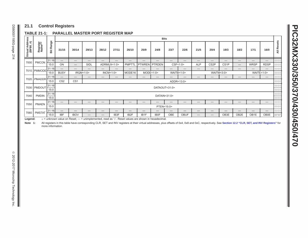
PIC32M
X330/350/370/430/450/470
DS
60001185G-page
214
2012-2017 M
icrochip Technology Inc.
21.1 Control RegistersTABLE 21-1: PARALLEL MASTER PORT REGISTER MAP
Virt
ual A
ddre
ss(B
F80_
#)
Reg
iste
rN
ame(1
)
Bit
Ran
ge
Bits
All
Res
ets
31/15 30/14 29/13 28/12 27/11 26/10 25/9 24/8 23/7 22/6 21/5 20/4 19/3 18/2 17/1 16/0
7000 PMCON31:16 — — — — — — — — — — — — — — — — 000015:0 ON — SIDL ADRMUX<1:0> PMPTTL PTWREN PTRDEN CSF<1:0> ALP CS2P CS1P — WRSP RDSP 0000
7010 PMMODE31:16 — — — — — — — — — — — — — — — — 000015:0 BUSY IRQM<1:0> INCM<1:0> MODE16 MODE<1:0> WAITB<1:0> WAITM<3:0> WAITE<1:0> 0000
7020 PMADDR31:16 — — — — — — — — — — — — — — — — 0000
15:0 CS2 CS1 ADDR<13:0> 0000
7030 PMDOUT31:16
DATAOUT<31:0>0000
15:0 0000
7040 PMDIN31:16
DATAIN<31:0>0000
15:0 0000
7050 PMAEN31:16 — — — — — — — — — — — — — — — — 0000
15:0 PTEN<15:0> 0000
7060 PMSTAT31:16 — — — — — — — — — — — — — — — — 000015:0 IBF IBOV — — IB3F IB2F IB1F IB0F OBE OBUF — — OB3E OB2E OB1E OB0E BFBF
Legend: x = unknown value on Reset; — = unimplemented, read as ‘0’. Reset values are shown in hexadecimal.Note 1: All registers in this table have corresponding CLR, SET and INV registers at their virtual addresses, plus offsets of 0x4, 0x8 and 0xC, respectively. See Section 12.2 “CLR, SET, and INV Registers” for
more information.

2012-2017 Microchip Technology Inc. DS60001185G-page 215
PIC32MX330/350/370/430/450/470
REGISTER 21-1: PMCON: PARALLEL PORT CONTROL REGISTER Bit
RangeBit
31/23/15/7Bit
30/22/14/6Bit
29/21/13/5Bit
28/20/12/4Bit
27/19/11/3Bit
26/18/10/2Bit
25/17/9/1Bit
24/16/8/0
31:24U-0 U-0 U-0 U-0 U-0 U-0 U-0 U-0
— — — — — — — —
23:16U-0 U-0 U-0 U-0 U-0 U-0 U-0 U-0
— — — — — — — —
15:8R/W-0 U-0 R/W-0 R/W-0 R/W-0 R/W-0 R/W-0 R/W-0
ON(1) — SIDL ADRMUX<1:0> PMPTTL PTWREN PTRDEN
7:0R/W-0 R/W-0 R/W-0 R/W-0 R/W-0 U-0 R/W-0 R/W-0
CSF<1:0>(2) ALP(2) CS2P(2) CS1P(2) — WRSP RDSP
Legend:R = Readable bit W = Writable bit U = Unimplemented bit, read as ‘0’-n = Value at POR ‘1’ = Bit is set ‘0’ = Bit is cleared x = Bit is unknown
bit 31-16 Unimplemented: Read as ‘0’bit 15 ON: Parallel Master Port Enable bit(1)
1 = PMP is enabled0 = PMP is disabled, no off-chip access performed
bit 14 Unimplemented: Read as ‘0’bit 13 SIDL: Stop in Idle Mode bit
1 = Discontinue module operation when device enters Idle mode0 = Continue module operation in Idle mode
bit 12-11 ADRMUX<1:0>: Address/Data Multiplexing Selection bits11 = Lower 8 bits of address are multiplexed on PMD<15:0> pins10 = All 16 bits of address are multiplexed on PMD<7:0> pins01 = Lower 8 bits of address are multiplexed on PMD<7:0> pins, upper bits are on PMA<15:8>00 = Address and data appear on separate pins
bit 10 PMPTTL: PMP Module TTL Input Buffer Select bit1 = PMP module uses TTL input buffers0 = PMP module uses Schmitt Trigger input buffer
bit 9 PTWREN: Write Enable Strobe Port Enable bit1 = PMWR/PMENB port is enabled0 = PMWR/PMENB port is disabled
bit 8 PTRDEN: Read/Write Strobe Port Enable bit1 = PMRD/PMWR port is enabled0 = PMRD/PMWR port is disabled
bit 7-6 CSF<1:0>: Chip Select Function bits(2)
11 = Reserved10 = PMCS1 and PMCS2 function as Chip Select01 = PMCS1 functions as address bit 14; PMCS2 functions as Chip Select00 = PMCS1 and PMCS2 function as address bits 14 and 15, respectively
bit 5 ALP: Address Latch Polarity bit(2)
1 = Active-high (PMALL and PMALH)0 = Active-low (PMALL and PMALH)
bit 4 CS2P: Chip Select 0 Polarity bit(2)
1 = Active-high (PMCS2)0 = Active-low (PMCS2)
Note 1: When using the 1:1 PBCLK divisor, the user software should not read/write the peripheral’s SFRs in the SYSCLK cycle immediately following the instruction that clears the module’s ON control bit.
2: These bits have no effect when their corresponding pins are used as address lines.

PIC32MX330/350/370/430/450/470
DS60001185G-page 216 2012-2017 Microchip Technology Inc.
bit 3 CS1P: Chip Select 0 Polarity bit(2)
1 = Active-high (PMCS1)0 = Active-low (PMCS1)
bit 2 Unimplemented: Read as ‘0’bit 1 WRSP: Write Strobe Polarity bit
For Slave Modes and Master mode 2 (MODE<1:0> = 00,01,10):1 = Write strobe active-high (PMWR)0 = Write strobe active-low (PMWR)
For Master mode 1 (MODE<1:0> = 11):1 = Enable strobe active-high (PMENB)0 = Enable strobe active-low (PMENB)
bit 0 RDSP: Read Strobe Polarity bitFor Slave modes and Master mode 2 (MODE<1:0> = 00,01,10):1 = Read Strobe active-high (PMRD)0 = Read Strobe active-low (PMRD)
For Master mode 1 (MODE<1:0> = 11):1 = Read/write strobe active-high (PMRD/PMWR)0 = Read/write strobe active-low (PMRD/PMWR)
REGISTER 21-1: PMCON: PARALLEL PORT CONTROL REGISTER (CONTINUED)
Note 1: When using the 1:1 PBCLK divisor, the user software should not read/write the peripheral’s SFRs in the SYSCLK cycle immediately following the instruction that clears the module’s ON control bit.
2: These bits have no effect when their corresponding pins are used as address lines.

2012-2017 Microchip Technology Inc. DS60001185G-page 217
PIC32MX330/350/370/430/450/470
REGISTER 21-2: PMMODE: PARALLEL PORT MODE REGISTER Bit
RangeBit
31/23/15/7Bit
30/22/14/6Bit
29/21/13/5Bit
28/20/12/4Bit
27/19/11/3Bit
26/18/10/2Bit
25/17/9/1Bit
24/16/8/0
31:24U-0 U-0 U-0 U-0 U-0 U-0 U-0 U-0
— — — — — — — —
23:16U-0 U-0 U-0 U-0 U-0 U-0 U-0 U-0
— — — — — — — —
15:8R-0 R/W-0 R/W-0 R/W-0 R/W-0 R/W-0 R/W-0 R/W-0
BUSY IRQM<1:0> INCM<1:0> MODE16 MODE<1:0>
7:0R/W-0 R/W-0 R/W-0 R/W-0 R/W-0 R/W-0 R/W-0 R/W-0
WAITB<1:0>(1) WAITM<3:0>(1) WAITE<1:0>(1)
Legend:R = Readable bit W = Writable bit U = Unimplemented bit, read as ‘0’-n = Value at POR ‘1’ = Bit is set ‘0’ = Bit is cleared x = Bit is unknown
bit 31-16 Unimplemented: Read as ‘0’bit 15 BUSY: Busy bit (Master mode only)
1 = Port is busy 0 = Port is not busy
bit 14-13 IRQM<1:0>: Interrupt Request Mode bits 11 = Reserved, do not use10 = Interrupt generated when Read Buffer 3 is read or Write Buffer 3 is written (Buffered PSP mode)
or on a read or write operation when PMA<1:0> =11 (Addressable Slave mode only)01 = Interrupt generated at the end of the read/write cycle00 = No Interrupt generated
bit 12-11 INCM<1:0>: Increment Mode bits 11 = Slave mode read and write buffers auto-increment (MODE<1:0> = 00 only)10 = Decrement ADDR<15:0> by 1 every read/write cycle(2)
01 = Increment ADDR<15:0> by 1 every read/write cycle(2)
00 = No increment or decrement of addressbit 10 MODE16: 8/16-bit Mode bit
1 = 16-bit mode: a read or write to the data register invokes a single 16-bit transfer0 = 8-bit mode: a read or write to the data register invokes a single 8-bit transfer
bit 9-8 MODE<1:0>: Parallel Port Mode Select bits11 = Master mode 1 (PMCSx, PMRD/PMWR, PMENB, PMA<x:0>, PMD<7:0> and PMD<8:15>(3))10 = Master mode 2 (PMCSx, PMRD, PMWR, PMA<x:0>, PMD<7:0> and PMD<8:15>(3))01 = Enhanced Slave mode, control signals (PMRD, PMWR, PMCS, PMD<7:0> and PMA<1:0>)00 = Legacy Parallel Slave Port, control signals (PMRD, PMWR, PMCS and PMD<7:0>)
bit 7-6 WAITB<1:0>: Data Setup to Read/Write Strobe Wait States bits(1)
11 = Data wait of 4 TPB; multiplexed address phase of 4 TPB10 = Data wait of 3 TPB; multiplexed address phase of 3 TPB01 = Data wait of 2 TPB; multiplexed address phase of 2 TPB00 = Data wait of 1 TPB; multiplexed address phase of 1 TPB (default)
Note 1: Whenever WAITM<3:0> = 0000, WAITB and WAITE bits are ignored and forced to 1 TPB cycle for a write operation; WAITB = 1 TPB cycle, WAITE = 0 TPB cycles for a read operation.
2: Address bits, A15 and A14, are not subject to automatic increment/decrement if configured as Chip Select CS2 and CS1.
3: These pins are active when MODE16 = 1 (16-bit mode).

PIC32MX330/350/370/430/450/470
DS60001185G-page 218 2012-2017 Microchip Technology Inc.
bit 5-2 WAITM<3:0>: Data Read/Write Strobe Wait States bits(1)
1111 = Wait of 16 TPB
•••0001 = Wait of 2 TPB0000 = Wait of 1 TPB (default)
bit 1-0 WAITE<1:0>: Data Hold After Read/Write Strobe Wait States bits(1)
11 = Wait of 4 TPB10 = Wait of 3 TPB01 = Wait of 2 TPB00 = Wait of 1 TPB (default)
For Read operations:11 = Wait of 3 TPB10 = Wait of 2 TPB01 = Wait of 1 TPB00 = Wait of 0 TPB (default)
REGISTER 21-2: PMMODE: PARALLEL PORT MODE REGISTER (CONTINUED)
Note 1: Whenever WAITM<3:0> = 0000, WAITB and WAITE bits are ignored and forced to 1 TPB cycle for a write operation; WAITB = 1 TPB cycle, WAITE = 0 TPB cycles for a read operation.
2: Address bits, A15 and A14, are not subject to automatic increment/decrement if configured as Chip Select CS2 and CS1.
3: These pins are active when MODE16 = 1 (16-bit mode).

2012-2017 Microchip Technology Inc. DS60001185G-page 219
PIC32MX330/350/370/430/450/470
REGISTER 21-3: PMADDR: PARALLEL PORT ADDRESS REGISTER Bit
RangeBit
31/23/15/7Bit
30/22/14/6Bit
29/21/13/5Bit
28/20/12/4Bit
27/19/11/3Bit
26/18/10/2Bit
25/17/9/1Bit
24/16/8/0
31:24U-0 U-0 U-0 U-0 U-0 U-0 U-0 U-0
— — — — — — — —
23:16U-0 U-0 U-0 U-0 U-0 U-0 U-0 U-0
— — — — — — — —
15:8R/W-0 R/W-0 R/W-0 R/W-0 R/W-0 R/W-0 R/W-0 R/W-0
CS2(1) CS1(3)ADDR<13:8>
ADDR15(2) ADDR14(4)
7:0 R/W-0 R/W-0 R/W-0 R/W-0 R/W-0 R/W-0 R/W-0 R/W-0
ADDR<7:0>
Legend:R = Readable bit W = Writable bit U = Unimplemented bit, read as ‘0’-n = Value at POR ‘1’ = Bit is set ‘0’ = Bit is cleared x = Bit is unknown
bit 31-16 Unimplemented: Read as ‘0’bit 15 CS2: Chip Select 2 bit(1)
1 = Chip Select 2 is active0 = Chip Select 2 is inactive
bit 15 ADDR<15>: Destination Address bit 15(2)
bit 14 CS1: Chip Select 1 bit(3)
1 = Chip Select 1 is active0 = Chip Select 1 is inactive
bit 14 ADDR<14>: Destination Address bit 14(4)
bit 13-0 ADDR<13:0>: Address bits
Note 1: When the CSF<1:0> bits (PMCON<7:6>) = 10 or 01.2: When the CSF<1:0> bits (PMCON<7:6>) = 00.3: When the CSF<1:0> bits (PMCON<7:6>) = 10.4: When the CSF<1:0> bits (PMCON<7:6>) = 00 or 01.

PIC32MX330/350/370/430/450/470
DS60001185G-page 220 2012-2017 Microchip Technology Inc.
REGISTER 21-4: PMAEN: PARALLEL PORT PIN ENABLE REGISTER Bit
RangeBit
31/23/15/7Bit
30/22/14/6Bit
29/21/13/5Bit
28/20/12/4Bit
27/19/11/3Bit
26/18/10/2Bit
25/17/9/1Bit
24/16/8/0
31:24U-0 U-0 U-0 U-0 U-0 U-0 U-0 U-0— — — — — — — —
23:16U-0 U-0 U-0 U-0 U-0 U-0 U-0 U-0— — — — — — — —
15:8R/W-0 R/W-0 R/W-0 R/W-0 R/W-0 R/W-0 R/W-0 R/W-0PTEN<15:14>(1) PTEN<13:8>
7:0R/W-0 R/W-0 R/W-0 R/W-0 R/W-0 R/W-0 R/W-0 R/W-0
PTEN<7:2> PTEN<1:0>(2)
Legend:R = Readable bit W = Writable bit U = Unimplemented bit, read as ‘0’-n = Value at POR ‘1’ = Bit is set ‘0’ = Bit is cleared x = Bit is unknown
bit 31-16 Unimplemented: Write ‘0’; ignore readbit 15-14 PTEN<15:14>: PMCSx Address Port Enable bits
1 = PMA15 and PMA14 function as either PMA<15:14> or PMCS2 and PMCS1(1)
0 = PMA15 and PMA14 function as port I/Obit 13-2 PTEN<13:2>: PMP Address Port Enable bits
1 = PMA<13:2> function as PMP address lines0 = PMA<13:2> function as port I/O
bit 1-0 PTEN<1:0>: PMALH/PMALL Address Port Enable bits1 = PMA1 and PMA0 function as either PMA<1:0> or PMALH and PMALL(2)
0 = PMA1 and PMA0 pads function as port I/O
Note 1: The use of these pins as PMA15/PMA14 or CS2/CS1 is selected by the CSF<1:0> bits (PMCON<7:6>).2: The use of these pins as PMA1/PMA0 or PMALH/PMALL depends on the Address/Data Multiplex mode
selected by the ADRMUX<1:0> bits in the PMCON register.

2012-2017 Microchip Technology Inc. DS60001185G-page 221
PIC32MX330/350/370/430/450/470
REGISTER 21-5: PMSTAT: PARALLEL PORT STATUS REGISTER (SLAVE MODES ONLY) Bit
RangeBit
31/23/15/7Bit
30/22/14/6Bit
29/21/13/5Bit
28/20/12/4Bit
27/19/11/3Bit
26/18/10/2Bit
25/17/9/1Bit
24/16/8/0
31:24U-0 U-0 U-0 U-0 U-0 U-0 U-0 U-0
— — — — — — — —
23:16U-0 U-0 U-0 U-0 U-0 U-0 U-0 U-0
— — — — — — — —
15:8R-0 R/W-0, HS, SC U-0 U-0 R-0 R-0 R-0 R-0
IBF IBOV — — IB3F IB2F IB1F IB0F
7:0R-1 R/W-0, HS, SC U-0 U-0 R-1 R-1 R-1 R-1
OBE OBUF — — OB3E OB2E OB1E OB0E
Legend: HS = Set by Hardware SC = Cleared by softwareR = Readable bit W = Writable bit U = Unimplemented bit, read as ‘0’-n = Value at POR ‘1’ = Bit is set ‘0’ = Bit is cleared x = Bit is unknown
bit 31-16 Unimplemented: Read as ‘0’bit 15 IBF: Input Buffer Full Status bit
1 = All writable input buffer registers are full0 = Some or all of the writable input buffer registers are empty
bit 14 IBOV: Input Buffer Overflow Status bit 1 = A write attempt to a full input byte buffer occurred (must be cleared in software)0 = No overflow occurred
bit 13-12 Unimplemented: Read as ‘0’bit 11-8 IBxF: Input Buffer ‘x’ Status Full bits
1 = Input Buffer contains data that has not been read (reading buffer will clear this bit)0 = Input Buffer does not contain any unread data
bit 7 OBE: Output Buffer Empty Status bit 1 = All readable output buffer registers are empty0 = Some or all of the readable output buffer registers are full
bit 6 OBUF: Output Buffer Underflow Status bit 1 = A read occurred from an empty output byte buffer (must be cleared in software)0 = No underflow occurred
bit 5-4 Unimplemented: Read as ‘0’bit 3-0 OBxE: Output Buffer ‘x’ Status Empty bits
1 = Output buffer is empty (writing data to the buffer will clear this bit)0 = Output buffer contains data that has not been transmitted

PIC32MX330/350/370/430/450/470
DS60001185G-page 222 2012-2017 Microchip Technology Inc.
NOTES:

2012-2017 Microchip Technology Inc. DS60001185G-page 223
PIC32MX330/350/370/430/450/47022.0 REAL-TIME CLOCK AND
CALENDAR (RTCC)Note: This data sheet summarizes the features
of the PIC32MX330/350/370/430/450/470 family of devices. It is not intended to be a comprehensive reference source. To complement the information in this data sheet, refer to Section 29. “Real-Time Clock and Calendar (RTCC)”(DS60001125), which is available from the Documentation > Reference Manual section of the Microchip PIC32 web site (www.microchip.com/pic32).
The PIC32 RTCC module is intended for applications in which accurate time must be maintained for extended periods of time with minimal or no CPU intervention. Low-power optimization provides extended battery lifetime while keeping track of time.
The following are key features of the RTCC module:
• Time: hours, minutes and seconds• 24-hour format (military time)• Visibility of one-half second period• Provides calendar: Weekday, date, month and
year• Alarm intervals are configurable for half of a
second, one second, 10 seconds, one minute, 10 minutes, one hour, one day, one week, one month and one year
• Alarm repeat with decrementing counter• Alarm with indefinite repeat: Chime• Year range: 2000 to 2099• Leap year correction• BCD format for smaller firmware overhead• Optimized for long-term battery operation• Fractional second synchronization• User calibration of the clock crystal frequency with
auto-adjust• Calibration range: 0.66 seconds error per month• Calibrates up to 260 ppm of crystal error• Requirements: External 32.768 kHz clock crystal• Alarm pulse or seconds clock output on
RTCC pin
FIGURE 22-1: RTCC BLOCK DIAGRAM
RTCC Prescalers
RTCC Timer
Comparator
Compare Registers
Repeat Counter
ALRMTIMEHR, MIN, SEC
ALRMDATEwith Masks
RTCC Interrupt Logic
AlarmEvent
32.768 kHz Inputfrom Secondary
0.5s
Alarm Pulse
Set RTCC Flag
RTCVAL
ALRMVAL
RTCC
RTCOE
Oscillator (SOSC)
CAL<9:0>
MONTH, DAY, WDAY
RTCTIMEHR, MIN, SEC
RTCDATEYEAR, MONTH, DAY, WDAY
Seconds Pulse
RTSECSEL
0
1
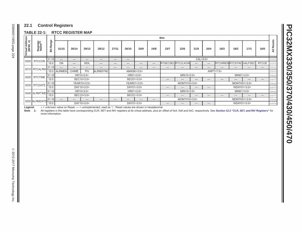
PIC32M
X330/350/370/430/450/470
DS
60001185G-page
224
2012-2017 M
icrochip Technology Inc.
22.1 Control RegistersTABLE 22-1: RTCC REGISTER MAP
Virt
ual A
ddre
ss(B
F80_
#)
Reg
iste
rN
ame(1
)
Bit
Ran
ge
Bits
All
Res
ets
31/15 30/14 29/13 28/12 27/11 26/10 25/9 24/8 23/7 22/6 21/5 20/4 19/3 18/2 17/1 16/0
0200 RTCCON31:16 — — — — — — CAL<9:0> 000015:0 ON — SIDL — — — — — RTSECSEL RTCCLKON — — RTCWREN RTCSYNC HALFSEC RTCOE 0000
0210 RTCALRM31:16 — — — — — — — — — — — — — — — — 000015:0 ALRMEN CHIME PIV ALRMSYNC AMASK<3:0> ARPT<7:0> 0000
0220 RTCTIME31:16 HR10<3:0> HR01<3:0> MIN10<3:0> MIN01<3:0> xxxx15:0 SEC10<3:0> SEC01<3:0> — — — — — — — — xx00
0230 RTCDATE31:16 YEAR10<3:0> YEAR01<3:0> MONTH10<3:0> MONTH01<3:0> xxxx15:0 DAY10<3:0> DAY01<3:0> — — — — WDAY01<3:0> xx00
0240 ALRMTIME31:16 HR10<3:0> HR01<3:0> MIN10<3:0> MIN01<3:0> xxxx15:0 SEC10<3:0> SEC01<3:0> — — — — — — — — xx00
0250 ALRMDATE31:16 — — — — — — — — MONTH10<3:0> MONTH01<3:0> 00xx15:0 DAY10<3:0> DAY01<3:0> — — — — WDAY01<3:0> xx0x
Legend: x = unknown value on Reset; — = unimplemented, read as ‘0’. Reset values are shown in hexadecimal.Note 1: All registers in this table have corresponding CLR, SET and INV registers at its virtual address, plus an offset of 0x4, 0x8 and 0xC, respectively. See Section 12.2 “CLR, SET, and INV Registers” for
more information.

2012-2017 Microchip Technology Inc. DS60001185G-page 225
PIC32MX330/350/370/430/450/470
REGISTER 22-1: RTCCON: RTC CONTROL REGISTER Bit
RangeBit
31/23/15/7Bit
30/22/14/6Bit
29/21/13/5Bit
28/20/12/4Bit
27/19/11/3Bit
26/18/10/2Bit
25/17/9/1Bit
24/16/8/0
31:24U-0 U-0 U-0 U-0 U-0 U-0 R/W-0 R/W-0
— — — — — — CAL<9:8>
23:16R/W-0 R/W-0 R/W-0 R/W-0 R/W-0 R/W-0 R/W-0 R/W-0
CAL<7:0>
15:8R/W-0 U-0 R/W-0 U-0 U-0 U-0 U-0 U-0
ON(1,2) — SIDL — — — — —
7:0R/W-0 R-0 U-0 U-0 R/W-0 R-0 R-0 R/W-0
RTSECSEL(3) RTCCLKON — — RTCWREN(4) RTCSYNC HALFSEC(5) RTCOE
Legend:R = Readable bit W = Writable bit U = Unimplemented bit, read as ‘0’-n = Value at POR ‘1’ = Bit is set ‘0’ = Bit is cleared x = Bit is unknown
bit 31-26 Unimplemented: Read as ‘0’bit 25-16 CAL<9:0>: RTC Drift Calibration bits, which contain a signed 10-bit integer value
0111111111 = Maximum positive adjustment, adds 511 RTC clock pulses every one minute•••0000000001 = Minimum positive adjustment, adds 1 RTC clock pulse every one minute0000000000 = No adjustment1111111111 = Minimum negative adjustment, subtracts 1 RTC clock pulse every one minute•••1000000000 = Maximum negative adjustment, subtracts 512 clock pulses every one minute
bit 15 ON: RTCC On bit(1,2)
1 = RTCC module is enabled0 = RTCC module is disabled
bit 14 Unimplemented: Read as ‘0’bit 13 SIDL: Stop in Idle Mode bit
1 = Disables the PBCLK to the RTCC when CPU enters in Idle mode0 = Continue normal operation in Idle mode
bit 12-8 Unimplemented: Read as ‘0’bit 7 RTSECSEL: RTCC Seconds Clock Output Select bit(3)
1 = RTCC Seconds Clock is selected for the RTCC pin0 = RTCC Alarm Pulse is selected for the RTCC pin
bit 6 RTCCLKON: RTCC Clock Enable Status bit1 = RTCC Clock is actively running0 = RTCC Clock is not running
bit 5-4 Unimplemented: Read as ‘0’
Note 1: The ON bit is only writable when RTCWREN = 1.2: When using the 1:1 PBCLK divisor, the user software should not read/write the peripheral’s SFRs in the
SYSCLK cycle immediately following the instruction that clears the module’s ON bit.3: Requires RTCOE = 1 (RTCCON<0>) for the output to be active.4: The RTCWREN bit can be set only when the write sequence is enabled.5: This bit is read-only. It is cleared to ‘0’ on a write to the seconds bit fields (RTCTIME<14:8>).
Note: This register is reset only on a Power-on Reset (POR).

PIC32MX330/350/370/430/450/470
DS60001185G-page 226 2012-2017 Microchip Technology Inc.
bit 3 RTCWREN: RTC Value Registers Write Enable bit(4)
1 = RTC Value registers can be written to by the user0 = RTC Value registers are locked out from being written to by the user
bit 2 RTCSYNC: RTCC Value Registers Read Synchronization bit1 = RTC Value registers can change while reading, due to a rollover ripple that results in an invalid data read
If the register is read twice and results in the same data, the data can be assumed to be valid0 = RTC Value registers can be read without concern about a rollover ripple
bit 1 HALFSEC: Half-Second Status bit(5)
1 = Second half period of a second0 = First half period of a second
bit 0 RTCOE: RTCC Output Enable bit1 = RTCC clock output is enabled – clock presented onto an I/O0 = RTCC clock output is disabled
REGISTER 22-1: RTCCON: RTC CONTROL REGISTER (CONTINUED)
Note 1: The ON bit is only writable when RTCWREN = 1.2: When using the 1:1 PBCLK divisor, the user software should not read/write the peripheral’s SFRs in the
SYSCLK cycle immediately following the instruction that clears the module’s ON bit.3: Requires RTCOE = 1 (RTCCON<0>) for the output to be active.4: The RTCWREN bit can be set only when the write sequence is enabled.5: This bit is read-only. It is cleared to ‘0’ on a write to the seconds bit fields (RTCTIME<14:8>).
Note: This register is reset only on a Power-on Reset (POR).

2012-2017 Microchip Technology Inc. DS60001185G-page 227
PIC32MX330/350/370/430/450/470
REGISTER 22-2: RTCALRM: RTC ALARM CONTROL REGISTER Bit
RangeBit
31/23/15/7Bit
30/22/14/6Bit
29/21/13/5Bit
28/20/12/4Bit
27/19/11/3Bit
26/18/10/2Bit
25/17/9/1Bit
24/16/8/0
31:24U-0 U-0 U-0 U-0 U-0 U-0 U-0 U-0
— — — — — — — —
23:16U-0 U-0 U-0 U-0 U-0 U-0 U-0 U-0
— — — — — — — —
15:8R/W-0 R/W-0 R/W-0 R-0 R/W-0 R/W-0 R/W-0 R/W-0
ALRMEN(1,2) CHIME(2) PIV(2) ALRMSYNC(3) AMASK<3:0>(3)
7:0R/W-0 R/W-0 R/W-0 R/W-0 R/W-0 R/W-0 R/W-0 R/W-0
ARPT<7:0>(3)
Legend:R = Readable bit W = Writable bit U = Unimplemented bit, read as ‘0’-n = Value at POR ‘1’ = Bit is set ‘0’ = Bit is cleared x = Bit is unknown
bit 31-16 Unimplemented: Read as ‘0’bit 15 ALRMEN: Alarm Enable bit(1,2)
1 = Alarm is enabled0 = Alarm is disabled
bit 14 CHIME: Chime Enable bit(2)
1 = Chime is enabled – ARPT<7:0> is allowed to rollover from 0x00 to 0xFF0 = Chime is disabled – ARPT<7:0> stops once it reaches 0x00
bit 13 PIV: Alarm Pulse Initial Value bit(2)
When ALRMEN = 0, PIV is writable and determines the initial value of the Alarm Pulse.When ALRMEN = 1, PIV is read-only and returns the state of the Alarm Pulse.
bit 12 ALRMSYNC: Alarm Sync bit(3)
1 = ARPT<7:0> and ALRMEN may change as a result of a half second rollover during a read. The ARPT must be read repeatedly until the same value is read twice. This must be done since multiple bits may be changing, which are then synchronized to the PB clock domain
0 = ARPT<7:0> and ALRMEN can be read without concerns of rollover because the prescaler is > 32 RTC clocks away from a half-second rollover
bit 11-8 AMASK<3:0>: Alarm Mask Configuration bits(3)
0000 = Every half-second0001 = Every second0010 = Every 10 seconds0011 = Every minute0100 = Every 10 minutes0101 = Every hour0110 = Once a day0111 = Once a week1000 = Once a month1001 = Once a year (except when configured for February 29, once every four years)1010 = Reserved; do not use1011 = Reserved; do not use11xx = Reserved; do not use
Note 1: Hardware clears the ALRMEN bit anytime the alarm event occurs, when ARPT<7:0> = 00 and CHIME = 0.
2: This field should not be written when the RTCC ON bit = ‘1’ (RTCCON<15>) and ALRMSYNC = 1.3: This assumes a CPU read will execute in less than 32 PBCLKs.
Note: This register is reset only on a Power-on Reset (POR).

PIC32MX330/350/370/430/450/470
DS60001185G-page 228 2012-2017 Microchip Technology Inc.
bit 7-0 ARPT<7:0>: Alarm Repeat Counter Value bits(3)
11111111 = Alarm will trigger 256 times•••00000000 = Alarm will trigger one timeThe counter decrements on any alarm event. The counter only rolls over from 0x00 to 0xFF if CHIME = 1.
REGISTER 22-2: RTCALRM: RTC ALARM CONTROL REGISTER (CONTINUED)
Note 1: Hardware clears the ALRMEN bit anytime the alarm event occurs, when ARPT<7:0> = 00 and CHIME = 0.
2: This field should not be written when the RTCC ON bit = ‘1’ (RTCCON<15>) and ALRMSYNC = 1.3: This assumes a CPU read will execute in less than 32 PBCLKs.
Note: This register is reset only on a Power-on Reset (POR).

2012-2017 Microchip Technology Inc. DS60001185G-page 229
PIC32MX330/350/370/430/450/470
REGISTER 22-3: RTCTIME: RTC TIME VALUE REGISTERBit
RangeBit
31/23/15/7Bit
30/22/14/6Bit
29/21/13/5Bit
28/20/12/4Bit
27/19/11/3Bit
26/18/10/2Bit
25/17/9/1Bit
24/16/8/0
31:24R/W-x R/W-x R/W-x R/W-x R/W-x R/W-x R/W-x R/W-x
HR10<3:0> HR01<3:0>
23:16R/W-x R/W-x R/W-x R/W-x R/W-x R/W-x R/W-x R/W-x
MIN10<3:0> MIN01<3:0>
15:8R/W-x R/W-x R/W-x R/W-x R/W-x R/W-x R/W-x R/W-x
SEC10<3:0> SEC01<3:0>
7:0U-0 U-0 U-0 U-0 U-0 U-0 U-0 U-0
— — — — — — — —
Legend:R = Readable bit W = Writable bit U = Unimplemented bit, read as ‘0’-n = Value at POR ‘1’ = Bit is set ‘0’ = Bit is cleared x = Bit is unknown
bit 31-28 HR10<3:0>: Binary-Coded Decimal Value of Hours bits, 10s place digits; contains a value from 0 to 2bit 27-24 HR01<3:0>: Binary-Coded Decimal Value of Hours bits, 1s place digit; contains a value from 0 to 9bit 23-20 MIN10<3:0>: Binary-Coded Decimal Value of Minutes bits, 10s place digits; contains a value from 0 to 5 bit 19-16 MIN01<3:0>: Binary-Coded Decimal Value of Minutes bits, 1s place digit; contains a value from 0 to 9bit 15-12 SEC10<3:0>: Binary-Coded Decimal Value of Seconds bits, 10s place digits; contains a value from 0 to 5 bit 11-8 SEC01<3:0>: Binary-Coded Decimal Value of Seconds bits, 1s place digit; contains a value from 0 to 9bit 7-0 Unimplemented: Read as ‘0’
Note: This register is only writable when RTCWREN = 1 (RTCCON<3>).

PIC32MX330/350/370/430/450/470
DS60001185G-page 230 2012-2017 Microchip Technology Inc.
REGISTER 22-4: RTCDATE: RTC DATE VALUE REGISTER
Bit Range
Bit31/23/15/7
Bit30/22/14/6
Bit29/21/13/5
Bit28/20/12/4
Bit27/19/11/3
Bit26/18/10/2
Bit25/17/9/1
Bit24/16/8/0
31:24R/W-x R/W-x R/W-x R/W-x R/W-x R/W-x R/W-x R/W-x
YEAR10<3:0> YEAR01<3:0>
23:16R/W-x R/W-x R/W-x R/W-x R/W-x R/W-x R/W-x R/W-x
MONTH10<3:0> MONTH01<3:0>
15:8R/W-x R/W-x R/W-x R/W-x R/W-x R/W-x R/W-x R/W-x
DAY10<3:0> DAY01<3:0>
7:0U-0 U-0 U-0 U-0 R/W-x R/W-x R/W-x R/W-x
— — — — WDAY01<3:0>
Legend:R = Readable bit W = Writable bit U = Unimplemented bit, read as ‘0’-n = Value at POR ‘1’ = Bit is set ‘0’ = Bit is cleared x = Bit is unknown
bit 31-28 YEAR10<3:0>: Binary-Coded Decimal Value of Years bits, 10s place digitsbit 27-24 YEAR01<3:0>: Binary-Coded Decimal Value of Years bits, 1s place digitbit 23-20 MONTH10<3:0>: Binary-Coded Decimal Value of Months bits, 10s place digits; contains a value of 0 or 1bit 19-16 MONTH01<3:0>: Binary-Coded Decimal Value of Months bits, 1s place digit; contains a value from 0 to 9bit 15-12 DAY10<3:0>: Binary-Coded Decimal Value of Days bits, 10s place digits; contains a value from 0 to 3bit 11-8 DAY01<3:0>: Binary-Coded Decimal Value of Days bits, 1s place digit; contains a value from 0 to 9bit 7-4 Unimplemented: Read as ‘0’bit 3-0 WDAY01<3:0>: Binary-Coded Decimal Value of Weekdays bits,1s place digit; contains a value from 0 to 6
Note: This register is only writable when RTCWREN = 1 (RTCCON<3>).

2012-2017 Microchip Technology Inc. DS60001185G-page 231
PIC32MX330/350/370/430/450/470
REGISTER 22-5: ALRMTIME: ALARM TIME VALUE REGISTER Bit
RangeBit
31/23/15/7Bit
30/22/14/6Bit
29/21/13/5Bit
28/20/12/4Bit
27/19/11/3Bit
26/18/10/2Bit
25/17/9/1Bit
24/16/8/0
31:24R/W-x R/W-x R/W-x R/W-x R/W-x R/W-x R/W-x R/W-x
HR10<3:0> HR01<3:0>
23:16R/W-x R/W-x R/W-x R/W-x R/W-x R/W-x R/W-x R/W-x
MIN10<3:0> MIN01<3:0>
15:8R/W-x R/W-x R/W-x R/W-x R/W-x R/W-x R/W-x R/W-x
SEC10<3:0> SEC01<3:0>
7:0U-0 U-0 U-0 U-0 U-0 U-0 U-0 U-0
— — — — — — — —
Legend:R = Readable bit W = Writable bit U = Unimplemented bit, read as ‘0’-n = Value at POR ‘1’ = Bit is set ‘0’ = Bit is cleared x = Bit is unknown
bit 31-28 HR10<3:0>: Binary Coded Decimal value of hours bits, 10s place digits; contains a value from 0 to 2bit 27-24 HR01<3:0>: Binary Coded Decimal value of hours bits, 1s place digit; contains a value from 0 to 9bit 23-20 MIN10<3:0>: Binary Coded Decimal value of minutes bits, 10s place digits; contains a value from 0 to 5bit 19-16 MIN01<3:0>: Binary Coded Decimal value of minutes bits, 1s place digit; contains a value from 0 to 9bit 15-12 SEC10<3:0>: Binary Coded Decimal value of seconds bits, 10s place digits; contains a value from 0 to 5bit 11-8 SEC01<3:0>: Binary Coded Decimal value of seconds bits, 1s place digit; contains a value from 0 to 9bit 7-0 Unimplemented: Read as ‘0’

PIC32MX330/350/370/430/450/470
DS60001185G-page 232 2012-2017 Microchip Technology Inc.
REGISTER 22-6: ALRMDATE: ALARM DATE VALUE REGISTER Bit
RangeBit
31/23/15/7Bit
30/22/14/6Bit
29/21/13/5Bit
28/20/12/4Bit
27/19/11/3Bit
26/18/10/2Bit
25/17/9/1Bit
24/16/8/0
31:24U-0 U-0 U-0 U-0 U-0 U-0 U-0 U-0
— — — — — — — —
23:16R/W-x R/W-x R/W-x R/W-x R/W-x R/W-x R/W-x R/W-x
MONTH10<3:0> MONTH01<3:0>
15:8R/W-x R/W-x R/W-x R/W-x R/W-x R/W-x R/W-x R/W-x
DAY10<1:0> DAY01<3:0>
7:0U-0 U-0 U-0 U-0 R/W-x R/W-x R/W-x R/W-x
— — — — WDAY01<3:0>
Legend:R = Readable bit W = Writable bit U = Unimplemented bit, read as ‘0’-n = Value at POR ‘1’ = Bit is set ‘0’ = Bit is cleared x = Bit is unknown
bit 31-24 Unimplemented: Read as ‘0’bit 23-20 MONTH10<3:0>: Binary Coded Decimal value of months bits, 10s place digits; contains a value of 0 or 1bit 19-16 MONTH01<3:0>: Binary Coded Decimal value of months bits, 1s place digit; contains a value from 0 to 9bit 15-12 DAY10<3:0>: Binary Coded Decimal value of days bits, 10s place digits; contains a value from 0 to 3bit 11-8 DAY01<3:0>: Binary Coded Decimal value of days bits, 1s place digit; contains a value from 0 to 9bit 7-4 Unimplemented: Read as ‘0’bit 3-0 WDAY01<3:0>: Binary Coded Decimal value of weekdays bits, 1s place digit; contains a value from 0 to 6

2012-2017 Microchip Technology Inc. DS60001185G-page 233
PIC32MX330/350/370/430/450/47023.0 10-BIT ANALOG-TO-DIGITAL
CONVERTER (ADC)Note: This data sheet summarizes the features
of the PIC32MX330/350/370/430/450/470 family of devices. It is not intended to be a comprehensive reference source. To complement the information in this data sheet, refer to Section 17. “10-bit Ana-log-to-Digital Converter (ADC)”(DS60001104), which is available from the Documentation > Reference Manual section of the Microchip PIC32 web site (www.microchip.com/pic32).
The 10-bit Analog-to-Digital Converter (ADC) includes the following features:• Successive Approximation Register (SAR)
conversion• Up to 1 Msps conversion speed• Up to 28 analog input pins• External voltage reference input pins• One unipolar, differential Sample and Hold
Amplifier (SHA) • Automatic Channel Scan mode• Selectable conversion trigger source• 16-word conversion result buffer• Selectable buffer fill modes• Eight conversion result format options • Operation during CPU Sleep and Idle modesA block diagram of the 10-bit ADC is illustrated in Figure 23-1. The 10-bit ADC has up to 28 analog input pins, designated AN0-AN27. In addition, there are two analog input pins for external voltage reference connections. These voltage reference inputs may be shared with other analog input pins and may be common to other analog module references.
FIGURE 23-1: ADC1 MODULE BLOCK DIAGRAM
SAR ADC
S&H
ADC1BUF0
ADC1BUF1
ADC1BUF2
ADC1BUFF
ADC1BUFE
IVREF(3)
CTMUT(2)
AN1
VREFL
CH0SB<4:0>
CH0NA CH0NB
+
-CH0SA<4:0>
ChannelScan
CSCNA
Alternate
VREF+(1) AVDD AVSSVREF-(1)
Note 1: VREF+ and VREF- inputs can be multiplexed with other analog inputs.2: Connected to the CTMU module. See Section 26.0 “Charge Time Measurement Unit (CTMU)” for more
information.3: See Section 25.0 “Comparator Voltage Reference (CVREF)” for more information.4: This selection is only used with CTMU capacitive and time measurement.
Input Selection
VREFH VREFL
VCFG<2:0>AN27
AN0
Open(4)
CTMUI(3)

PIC32MX330/350/370/430/450/470
DS60001185G-page 234 2012-2017 Microchip Technology Inc.
FIGURE 23-2: ADC CONVERSION CLOCK PERIOD BLOCK DIAGRAM
1
0
Div 2
TPB (2)
ADC ConversionClock Multiplier
2, 4,..., 512
ADRC
TAD
8
ADCS<7:0>
FRC(1)
Note 1: See Section 31.0 “Electrical Characteristics” for the exact FRC clock value.2: Refer to Figure 8-1 in Section 8.0 “Oscillator Configuration” for more information.

2012-2017 M
icrochip Technology Inc.D
S60001185G
-page
235
PIC32M
X330/350/370/430/450/470
23.1 Control Registers TABLE 23-1: ADC REGISTER MAP
Virt
ual A
ddre
ss(B
F80_
#)
RegisterName
Bit
Ran
ge
Bits
All
Res
ets
31/15 30/14 29/13 28/12 27/11 26/10 25/9 24/8 23/7 22/6 21/5 20/4 19/3 18/2 17/1 16/0
9000 AD1CON1(1) 31:16 — — — — — — — — — — — — — — — — 0000
15:0 ON — SIDL — — FORM<2:0> SSRC<2:0> CLRASAM — ASAM SAMP DONE 0000
9010 AD1CON2(1) 31:16 — — — — — — — — — — — — — — — — 0000
15:0 VCFG<2:0> OFFCAL — CSCNA — — BUFS — SMPI<3:0> BUFM ALTS 0000
9020 AD1CON3(1) 31:16 — — — — — — — — — — — — — — — — 0000
15:0 ADRC — — SAMC<4:0> ADCS<7:0> 0000
9040 AD1CHS(1) 31:16 CH0NB — — CH0SB<4:0> CH0NA — — CH0SA<4:0> 0000
15:0 — — — — — — — — — — — — — — — — 0000
9050 AD1CSSL(1) 31:16 — CSSL30 CSSL29 CSSL28 CSSL27 CSSL26 CSSL25 CSSL24 CSSL23 CSSL22 CSSL21 CSSL20 CSSL19 CSSL18 CSSL17 CSSL16 0000
15:0 CSSL15 CSSL14 CSSL13 CSSL12 CSSL11 CSSL10 CSSL9 CSSL8 CSSL7 CSSL6 CSSL5 CSSL4 CSSL3 CSSL2 CSSL1 CSSL0 0000
9070 ADC1BUF031:16
ADC Result Word 0 (ADC1BUF0<31:0>)0000
15:0 0000
9080 ADC1BUF131:16
ADC Result Word 1 (ADC1BUF1<31:0>)0000
15:0 0000
9090 ADC1BUF231:16
ADC Result Word 2 (ADC1BUF2<31:0>)0000
15:0 0000
90A0 ADC1BUF331:16
ADC Result Word 3 (ADC1BUF3<31:0>)0000
15:0 0000
90B0 ADC1BUF431:16
ADC Result Word 4 (ADC1BUF4<31:0>)0000
15:0 0000
90C0 ADC1BUF531:16
ADC Result Word 5 (ADC1BUF5<31:0>)0000
15:0 0000
90D0 ADC1BUF631:16
ADC Result Word 6 (ADC1BUF6<31:0>)0000
15:0 0000
90E0 ADC1BUF731:16
ADC Result Word 7 (ADC1BUF7<31:0>)0000
15:0 0000
90F0 ADC1BUF831:16
ADC Result Word 8 (ADC1BUF8<31:0>)0000
15:0 0000
9100 ADC1BUF931:16
ADC Result Word 9 (ADC1BUF9<31:0>)0000
15:0 0000
Legend: x = unknown value on Reset; — = unimplemented, read as ‘0’. Reset values are shown in hexadecimal.Note 1: All registers in this table have corresponding CLR, SET and INV registers at their virtual addresses, plus offsets of 0x4, 0x8 and 0xC, respectively. See Section 12.2 “CLR, SET, and INV Registers” for
details.
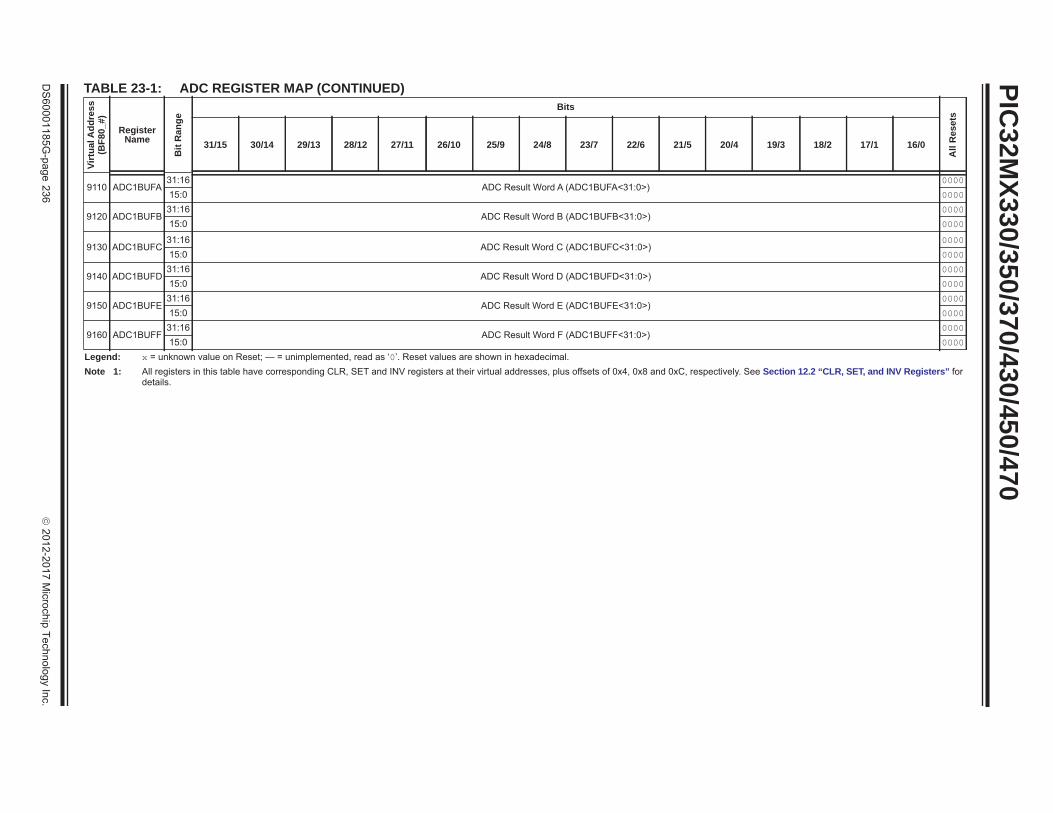
PIC32M
X330/350/370/430/450/470
DS
60001185G-page
236
2012-2017 M
icrochip Technology Inc.
9110 ADC1BUFA31:16
ADC Result Word A (ADC1BUFA<31:0>)0000
15:0 0000
9120 ADC1BUFB31:16
ADC Result Word B (ADC1BUFB<31:0>)0000
15:0 0000
9130 ADC1BUFC31:16
ADC Result Word C (ADC1BUFC<31:0>)0000
15:0 0000
9140 ADC1BUFD31:16
ADC Result Word D (ADC1BUFD<31:0>)0000
15:0 0000
9150 ADC1BUFE31:16
ADC Result Word E (ADC1BUFE<31:0>)0000
15:0 0000
9160 ADC1BUFF31:16
ADC Result Word F (ADC1BUFF<31:0>)0000
15:0 0000
TABLE 23-1: ADC REGISTER MAP (CONTINUED)Vi
rtua
l Add
ress
(BF8
0_#)
RegisterName
Bit
Ran
ge
Bits
All
Res
ets
31/15 30/14 29/13 28/12 27/11 26/10 25/9 24/8 23/7 22/6 21/5 20/4 19/3 18/2 17/1 16/0
Legend: x = unknown value on Reset; — = unimplemented, read as ‘0’. Reset values are shown in hexadecimal.Note 1: All registers in this table have corresponding CLR, SET and INV registers at their virtual addresses, plus offsets of 0x4, 0x8 and 0xC, respectively. See Section 12.2 “CLR, SET, and INV Registers” for
details.

2012-2017 Microchip Technology Inc. DS60001185G-page 237
PIC32MX330/350/370/430/450/470
REGISTER 23-1: AD1CON1: ADC CONTROL REGISTER 1 Bit
RangeBit
31/23/15/7Bit
30/22/14/6Bit
29/21/13/5Bit
28/20/12/4Bit
27/19/11/3Bit
26/18/10/2Bit
25/17/9/1Bit
24/16/8/0
31:24U-0 U-0 U-0 U-0 U-0 U-0 U-0 U-0
— — — — — — — —
23:16U-0 U-0 U-0 U-0 U-0 U-0 U-0 U-0
— — — — — — — —
15:8R/W-0 U-0 R/W-0 U-0 U-0 R/W-0 R/W-0 R/W-0
ON(1) — SIDL — — FORM<2:0>
7:0R/W-0 R/W-0 R/W-0 R/W-0 U-0 R/W-0 R/W-0, HSC R/C-0, HSC
SSRC<2:0> CLRASAM — ASAM SAMP(2) DONE(3)
Legend:R = Readable bit W = Writable bit U = Unimplemented bit, read as ‘0’-n = Value at POR ‘1’ = Bit is set ‘0’ = Bit is cleared x = Bit is unknown
bit 31-16 Unimplemented: Read as ‘0’bit 15 ON: ADC Operating Mode bit(1)
1 = ADC module is operating0 = ADC module is not operating
bit 14 Unimplemented: Read as ‘0’bit 13 SIDL: Stop in Idle Mode bit
1 = Discontinue module operation when device enters Idle mode0 = Continue module operation in Idle mode
bit 12-11 Unimplemented: Read as ‘0’bit 10-8 FORM<2:0>: Data Output Format bits
011 = Signed Fractional 16-bit (DOUT = 0000 0000 0000 0000 sddd dddd dd00 0000)010 = Fractional 16-bit (DOUT = 0000 0000 0000 0000 dddd dddd dd00 0000)001 = Signed Integer 16-bit (DOUT = 0000 0000 0000 0000 ssss sssd dddd dddd)000 = Integer 16-bit (DOUT = 0000 0000 0000 0000 0000 00dd dddd dddd)111 = Signed Fractional 32-bit (DOUT = sddd dddd dd00 0000 0000 0000 0000)110 = Fractional 32-bit (DOUT = dddd dddd dd00 0000 0000 0000 0000 0000)101 = Signed Integer 32-bit (DOUT = ssss ssss ssss ssss ssss sssd dddd dddd)100 = Integer 32-bit (DOUT = 0000 0000 0000 0000 0000 00dd dddd dddd)
bit 7-5 SSRC<2:0>: Conversion Trigger Source Select bits111 = Internal counter ends sampling and starts conversion (auto convert)110 = Reserved101 = Reserved100 = Reserved011 = CTMU ends sampling and starts conversion010 = Timer 3 period match ends sampling and starts conversion001 = Active transition on INT0 pin ends sampling and starts conversion000 = Clearing SAMP bit ends sampling and starts conversion
Note 1: When using the 1:1 PBCLK divisor, the user software should not read/write the peripheral’s SFRs in the SYSCLK cycle immediately following the instruction that clears the module’s ON bit.
2: If ASAM = 0, software can write a ‘1’ to start sampling. This bit is automatically set by hardware if ASAM = 1. If SSRC = 0, software can write a ‘0’ to end sampling and start conversion. If SSRC 0, this bit is automatically cleared by hardware to end sampling and start conversion.
3: This bit is automatically set by hardware when ADC is complete. Software can write a ‘0’ to clear this bit (a write of ‘1’ is not allowed). Clearing this bit does not affect any operation already in progress. This bit is automatically cleared by hardware at the start of a new conversion.

PIC32MX330/350/370/430/450/470
DS60001185G-page 238 2012-2017 Microchip Technology Inc.
bit 4 CLRASAM: Stop Conversion Sequence bit (when the first ADC interrupt is generated)1 = Stop conversions when the first ADC interrupt is generated. Hardware clears the ASAM bit when the
ADC interrupt is generated.0 = Normal operation, buffer contents will be overwritten by the next conversion sequence
bit 3 Unimplemented: Read as ‘0’bit 2 ASAM: ADC Sample Auto-Start bit
1 = Sampling begins immediately after last conversion completes; SAMP bit is automatically set.0 = Sampling begins when SAMP bit is set
bit 1 SAMP: ADC Sample Enable bit(2)
1 = The ADC sample and hold amplifier is sampling0 = The ADC sample/hold amplifier is holdingWhen ASAM = 0, writing ‘1’ to this bit starts sampling. When SSRC = 000, writing ‘0’ to this bit will end sampling and start conversion.
bit 0 DONE: Analog-to-Digital Conversion Status bit(3)
1 = Analog-to-digital conversion is done0 = Analog-to-digital conversion is not done or has not startedClearing this bit will not affect any operation in progress.
REGISTER 23-1: AD1CON1: ADC CONTROL REGISTER 1 (CONTINUED)
Note 1: When using the 1:1 PBCLK divisor, the user software should not read/write the peripheral’s SFRs in the SYSCLK cycle immediately following the instruction that clears the module’s ON bit.
2: If ASAM = 0, software can write a ‘1’ to start sampling. This bit is automatically set by hardware if ASAM = 1. If SSRC = 0, software can write a ‘0’ to end sampling and start conversion. If SSRC 0, this bit is automatically cleared by hardware to end sampling and start conversion.
3: This bit is automatically set by hardware when ADC is complete. Software can write a ‘0’ to clear this bit (a write of ‘1’ is not allowed). Clearing this bit does not affect any operation already in progress. This bit is automatically cleared by hardware at the start of a new conversion.

2012-2017 Microchip Technology Inc. DS60001185G-page 239
PIC32MX330/350/370/430/450/470
REGISTER 23-2: AD1CON2: ADC CONTROL REGISTER 2 Bit
RangeBit
31/23/15/7Bit
30/22/14/6Bit
29/21/13/5Bit
28/20/12/4Bit
27/19/11/3Bit
26/18/10/2Bit
25/17/9/1Bit
24/16/8/0
31:24U-0 U-0 U-0 U-0 U-0 U-0 U-0 U-0
— — — — — — — —
23:16U-0 U-0 U-0 U-0 U-0 U-0 U-0 U-0
— — — — — — — —
15:8R/W-0 R/W-0 R/W-0 R/W-0 U-0 R/W-0 U-0 U-0
VCFG<2:0> OFFCAL — CSCNA — —
7:0R-0 U-0 R/W-0 R/W-0 R/W-0 R/W-0 R/W-0 R/W-0
BUFS — SMPI<3:0> BUFM ALTS
Legend:R = Readable bit W = Writable bit U = Unimplemented bit, read as ‘0’-n = Value at POR ‘1’ = Bit is set ‘0’ = Bit is cleared x = Bit is unknown
bit 31-16 Unimplemented: Read as ‘0’bit 15-13 VCFG<2:0>: Voltage Reference Configuration bits
VREFH VREFL
000 AVDD AVss001 External VREF+ pin AVSS
010 AVDD External VREF- pin011 External VREF+ pin External VREF- pin1xx AVDD AVSS
bit 12 OFFCAL: Input Offset Calibration Mode Select bit1 = Enable Offset Calibration mode
Positive and negative inputs of the sample and hold amplifier are connected to VREFL0 = Disable Offset Calibration mode
The inputs to the sample and hold amplifier are controlled by AD1CHS or AD1CSSLbit 11 Unimplemented: Read as ‘0’bit 10 CSCNA: Input Scan Select bit
1 = Scan inputs0 = Do not scan inputs
bit 9-8 Unimplemented: Read as ‘0’bit 7 BUFS: Buffer Fill Status bit
Only valid when BUFM = 1.1 = ADC is currently filling buffer 0x8-0xF, user should access data in 0x0-0x70 = ADC is currently filling buffer 0x0-0x7, user should access data in 0x8-0xF
bit 6 Unimplemented: Read as ‘0’bit 5-2 SMPI<3:0>: Sample/Convert Sequences Per Interrupt Selection bits
1111 = Interrupts at the completion of conversion for each 16th sample/convert sequence1110 = Interrupts at the completion of conversion for each 15th sample/convert sequence•••0001 = Interrupts at the completion of conversion for each 2nd sample/convert sequence0000 = Interrupts at the completion of conversion for each sample/convert sequence
bit 1 BUFM: ADC Result Buffer Mode Select bit1 = Buffer configured as two 8-word buffers, ADC1BUF7-ADC1BUF0, ADC1BUFF-ADCBUF80 = Buffer configured as one 16-word buffer ADC1BUFF-ADC1BUF0
bit 0 ALTS: Alternate Input Sample Mode Select bit1 = Uses Sample A input multiplexer settings for first sample, then alternates between Sample B and
Sample A input multiplexer settings for all subsequent samples0 = Always use Sample A input multiplexer settings

PIC32MX330/350/370/430/450/470
DS60001185G-page 240 2012-2017 Microchip Technology Inc.
REGISTER 23-3: AD1CON3: ADC CONTROL REGISTER 3 Bit
RangeBit
31/23/15/7Bit
30/22/14/6Bit
29/21/13/5Bit
28/20/12/4Bit
27/19/11/3Bit
26/18/10/2Bit
25/17/9/1Bit
24/16/8/0
31:24U-0 U-0 U-0 U-0 U-0 U-0 U-0 U-0
— — — — — — — —
23:16U-0 U-0 U-0 U-0 U-0 U-0 U-0 U-0
— — — — — — — —
15:8R/W-0 U-0 U-0 R/W-0 R/W-0 R/W-0 R/W-0 R/W-0
ADRC — — SAMC<4:0>(1)
7:0R/W-0 R/W-0 R/W-0 R/W-0 R/W-0 R/W-0 R/W R/W-0
ADCS<7:0>(2)
Legend:R = Readable bit W = Writable bit U = Unimplemented bit, read as ‘0’-n = Value at POR ‘1’ = Bit is set ‘0’ = Bit is cleared x = Bit is unknown
bit 31-16 Unimplemented: Read as ‘0’bit 15 ADRC: ADC Conversion Clock Source bit
1 = Clock derived from FRC0 = Clock derived from Peripheral Bus Clock (PBCLK)
bit 14-13 Unimplemented: Read as ‘0’bit 12-8 SAMC<4:0>: Auto-Sample Time bits(1)
11111 =31 TAD
•••00001 =1 TAD00000 =0 TAD (Not allowed)
bit 7-0 ADCS<7:0>: ADC Conversion Clock Select bits(2)
11111111 =TPB • 2 • (ADCS<7:0> + 1) = 512 • TPB = TAD
•••00000001 =TPB • 2 • (ADCS<7:0> + 1) = 4 • TPB = TAD00000000 =TPB • 2 • (ADCS<7:0> + 1) = 2 • TPB = TAD
Note 1: This bit is only used if the SSRC<2:0> bits (AD1CON1<7:5>) = 111.2: This bit is not used if the ADRC bit (AD1CON3<15>) = 1.

2012-2017 Microchip Technology Inc. DS60001185G-page 241
PIC32MX330/350/370/430/450/470
REGISTER 23-4: AD1CHS: ADC INPUT SELECT REGISTER Bit
RangeBit
31/23/15/7Bit
30/22/14/6Bit
29/21/13/5Bit
28/20/12/4Bit
27/19/11/3Bit
26/18/10/2Bit
25/17/9/1Bit
24/16/8/0
31:24R/W-0 U-0 U-0 R/W-0 R/W-0 R/W-0 R/W-0 R/W-0
CH0NB — — CH0SB<4:0>
23:16R/W-0 U-0 U-0 R/W-0 R/W-0 R/W-0 R/W-0 R/W-0
CH0NA(3) — — CH0SA<4:0>
15:8U-0 U-0 U-0 U-0 U-0 U-0 U-0 U-0
— — — — — — — —
7:0U-0 U-0 U-0 U-0 U-0 U-0 U-0 U-0
— — — — — — — —
Legend:R = Readable bit W = Writable bit U = Unimplemented bit, read as ‘0’-n = Value at POR ‘1’ = Bit is set ‘0’ = Bit is cleared x = Bit is unknown
bit 31 CH0NB: Negative Input Select bit for Sample B1 = Channel 0 negative input is AN10 = Channel 0 negative input is VREFL
bit 30-29 Unimplemented: Read as ‘0’bit 28-24 CH0SB<4:0>: Positive Input Select bits for Sample B
11110 = Channel 0 positive input is Open(1)
11101 = Channel 0 positive input is CTMU temperature sensor (CTMUT)(2)
11100 = Channel 0 positive input is IVREF(3)
11011 = Channel 0 positive input is AN27•••00001 = Channel 0 positive input is AN100000 = Channel 0 positive input is AN0
bit 23 CH0NA: Negative Input Select bit for Sample A Multiplexer Setting(3)
1 = Channel 0 negative input is AN10 = Channel 0 negative input is VREFL
bit 22-21 Unimplemented: Read as ‘0’bit 20-16 CH0SA<4:0>: Positive Input Select bits for Sample A Multiplexer Setting
11110 = Channel 0 positive input is Open(1)
11101 = Channel 0 positive input is CTMU temperature sensor (CTMUT)(2)
11100 = Channel 0 positive input is IVREF(3)
11011 = Channel 0 positive input is AN27•••00001 = Channel 0 positive input is AN100000 = Channel 0 positive input is AN0
bit 15-0 Unimplemented: Read as ‘0’
Note 1: This selection is only used with CTMU capacitive and time measurement.2: See Section 26.0 “Charge Time Measurement Unit (CTMU)” for more information.3: See Section 25.0 “Comparator Voltage Reference (CVREF)” for more information.

PIC32MX330/350/370/430/450/470
DS60001185G-page 242 2012-2017 Microchip Technology Inc.
REGISTER 23-5: AD1CSSL: ADC INPUT SCAN SELECT REGISTER Bit
RangeBit
31/23/15/7Bit
30/22/14/6Bit
29/21/13/5Bit
28/20/12/4Bit
27/19/11/3Bit
26/18/10/2Bit
25/17/9/1Bit
24/16/8/0
31:24U-0 R/W-0 R/W-0 R/W-0 R/W-0 R/W-0 R/W-0 R/W-0
— CSSL30 CSSL29 CSSL28 CSSL27 CSSL26 CSSL25 CSSL24
23:16R/W-0 R/W-0 R/W-0 R/W-0 R/W-0 R/W-0 R/W-0 R/W-0
CSSL23 CSSL21 CSSL21 CSSL20 CSSL19 CSSL18 CSSL17 CSSL16
15:8R/W-0 R/W-0 R/W-0 R/W-0 R/W-0 R/W-0 R/W-0 R/W-0
CSSL15 CSSL14 CSSL13 CSSL12 CSSL11 CSSL10 CSSL9 CSSL8
7:0R/W-0 R/W-0 R/W-0 R/W-0 R/W-0 R/W-0 R/W-0 R/W-0
CSSL7 CSSL6 CSSL5 CSSL4 CSSL3 CSSL2 CSSL1 CSSL0
Legend:R = Readable bit W = Writable bit U = Unimplemented bit, read as ‘0’-n = Value at POR ‘1’ = Bit is set ‘0’ = Bit is cleared x = Bit is unknown
bit 31-16 Unimplemented: Read as ‘0’bit 15-0 CSSL<30:0>: ADC Input Pin Scan Selection bits(1,2)
1 = Select ANx for input scan0 = Skip ANx for input scan
Note 1: CSSL = ANx, where x = 0-27; CSSL30 selects Vss for scan; CSSL29 selects CTMU input for scan; CSSL28 selects IVREF for scan.
2: On devices with less than 28 analog inputs, all CSSLx bits can be selected; however, inputs selected for scan without a corresponding input on the device will convert to VREFL.

2012-2017 Microchip Technology Inc. DS60001185G-page 243
PIC32MX330/350/370/430/450/47024.0 COMPARATOR
Note: This data sheet summarizes the features of the PIC32MX330/350/370/430/450/470 family of devices. It is not intended to be a comprehensive reference source. To complement the information in this data sheet, refer to Section 19. “Comparator” (DS60001110), which is available from the Documentation > Reference Manual section of the Microchip PIC32 web site (www.microchip.com/pic32).
The Analog Comparator module contains two comparators that can be configured in a variety of ways.
The following are key features of the Comparator module:
• Selectable inputs available include:- Analog inputs multiplexed with I/O pins- On-chip internal absolute voltage reference
(IVREF)- Comparator voltage reference (CVREF)
• Outputs can be Inverted• Selectable interrupt generationA block diagram of the comparator module is provided in Figure 24-1.
FIGURE 24-1: COMPARATOR BLOCK DIAGRAM
CVREF(1)
IVREF (1.2V)
C2IND
C2INA
C2OUTCMP2
COE
CREF
CCH<1:0>
CPOL
C2INC
C2INB
C1IND
C1INA
C1OUTCMP1
COE
CREF
CCH<1:0>
CPOL
C1INC
C1INB
CMSTAT<C1OUT>CM1CON<COUT>
CMSTAT<C2OUT>CM2CON<COUT>
To CTMU module(Pulse Generator)
Note 1: Internally connected. See Section 25.0 “Comparator Voltage Reference (CVREF)” for more information.

PIC32M
X330/350/370/430/450/470
DS
60001185G-page
244
2012-2017 M
icrochip Technology Inc.
24.1 Control RegistersTABLE 24-1: COMPARATOR REGISTER MAP
Virt
ual A
ddre
ss(B
F80_
#)
Reg
iste
rN
ame(1
)
Bit
Ran
ge
Bits
All
Res
ets
31/15 30/14 29/13 28/12 27/11 26/10 25/9 24/8 23/7 22/6 21/5 20/4 19/3 18/2 17/1 16/0
A000 CM1CON31:16 — — — — — — — — — — — — — — — — 000015:0 ON COE CPOL — — — — COUT EVPOL<1:0> — CREF — — CCH<1:0> E1C3
A010 CM2CON31:16 — — — — — — — — — — — — — — — — 000015:0 ON COE CPOL — — — — COUT EVPOL<1:0> — CREF — — CCH<1:0> E1C3
A060 CMSTAT31:16 — — — — — — — — — — — — — — — — 000015:0 — — SIDL — — — — — — — — — — — C2OUT C1OUT 0000
Legend: x = unknown value on Reset; — = unimplemented, read as ‘0’. Reset values are shown in hexadecimal.Note 1: All registers in this table have corresponding CLR, SET and INV registers at their virtual addresses, plus offsets of 0x4, 0x8 and 0xC, respectively. See Section 12.2 “CLR, SET, and INV Registers” for
more information.

2012-2017 Microchip Technology Inc. DS60001185G-page 245
PIC32MX330/350/370/430/450/470
REGISTER 24-1: CMxCON: COMPARATOR CONTROL REGISTER Bit
RangeBit
31/23/15/7Bit
30/22/14/6Bit
29/21/13/5Bit
28/20/12/4Bit
27/19/11/3Bit
26/18/10/2Bit
25/17/9/1Bit
24/16/8/0
31:24U-0 U-0 U-0 U-0 U-0 U-0 U-0 U-0
— — — — — — — —
23:16U-0 U-0 U-0 U-0 U-0 U-0 U-0 U-0
— — — — — — — —
15:8R/W-0 R/W-0 R/W-0 U-0 U-0 U-0 U-0 R-0
ON(1) COE CPOL(2) — — — — COUT
7:0R/W-1 R/W-1 U-0 R/W-0 U-0 U-0 R/W-1 R/W-1
EVPOL<1:0> — CREF — — CCH<1:0>
Legend:R = Readable bit W = Writable bit U = Unimplemented bit, read as ‘0’-n = Value at POR ‘1’ = Bit is set ‘0’ = Bit is cleared x = Bit is unknown
bit 31-16 Unimplemented: Read as ‘0’bit 15 ON: Comparator ON bit(1)
1 = Module is enabled. Setting this bit does not affect the other bits in this register0 = Module is disabled and does not consume current. Clearing this bit does not affect the other bits in this
registerbit 14 COE: Comparator Output Enable bit
1 = Comparator output is driven on the output CxOUT pin0 = Comparator output is not driven on the output CxOUT pin
bit 13 CPOL: Comparator Output Inversion bit(2)
1 = Output is inverted0 = Output is not inverted
bit 12-9 Unimplemented: Read as ‘0’bit 8 COUT: Comparator Output bit
1 = Output of the Comparator is a ‘1’0 = Output of the Comparator is a ‘0’
bit 7-6 EVPOL<1:0>: Interrupt Event Polarity Select bits11 = Comparator interrupt is generated on a low-to-high or high-to-low transition of the comparator output10 = Comparator interrupt is generated on a high-to-low transition of the comparator output01 = Comparator interrupt is generated on a low-to-high transition of the comparator output00 = Comparator interrupt generation is disabled
bit 5 Unimplemented: Read as ‘0’bit 4 CREF: Comparator Positive Input Configure bit
1 = Comparator non-inverting input is connected to the internal CVREF0 = Comparator non-inverting input is connected to the CXINA pin
bit 3-2 Unimplemented: Read as ‘0’bit 1-0 CCH<1:0>: Comparator Negative Input Select bits for Comparator
11 = Comparator inverting input is connected to the IVREF10 = Comparator inverting input is connected to the CxIND pin01 = Comparator inverting input is connected to the CxINC pin00 = Comparator inverting input is connected to the CxINB pin
Note 1: When using the 1:1 PBCLK divisor, the user’s software should not read/write the peripheral’s SFRs in the SYSCLK cycle immediately following the instruction that clears the module’s ON bit.
2: Setting this bit will invert the signal to the comparator interrupt generator as well. This will result in an interrupt being generated on the opposite edge from the one selected by EVPOL<1:0>.

PIC32MX330/350/370/430/450/470
DS60001185G-page 246 2012-2017 Microchip Technology Inc.
REGISTER 24-2: CMSTAT: COMPARATOR STATUS REGISTERBit
RangeBit
31/23/15/7Bit
30/22/14/6Bit
29/21/13/5Bit
28/20/12/4Bit
27/19/11/3Bit
26/18/10/2Bit
25/17/9/1Bit
24/16/8/0
31:24U-0 U-0 U-0 U-0 U-0 U-0 U-0 U-0
— — — — — — — —
23:16U-0 U-0 U-0 U-0 U-0 U-0 U-0 U-0
— — — — — — — —
15:8U-0 U-0 R/W-0 U-0 U-0 U-0 U-0 U-0
— — SIDL — — — — —
7:0U-0 U-0 U-0 U-0 U-0 U-0 R-0 R-0
— — — — — — C2OUT C1OUT
Legend:R = Readable bit W = Writable bit U = Unimplemented bit, read as ‘0’
-n = Value at POR ‘1’ = Bit is set ‘0’ = Bit is cleared x = Bit is unknown
bit 31-14 Unimplemented: Read as ‘0’
bit 13 SIDL: Stop in IDLE Control bit1 = All Comparator modules are disabled in IDLE mode0 = All Comparator modules continue to operate in the IDLE mode
bit 12-2 Unimplemented: Read as ‘0’
bit 1 C2OUT: Comparator Output bit1 = Output of Comparator 2 is a ‘1’0 = Output of Comparator 2 is a ‘0’
bit 0 C1OUT: Comparator Output bit1 = Output of Comparator 1 is a ‘1’0 = Output of Comparator 1 is a ‘0’

2012-2017 Microchip Technology Inc. DS60001185G-page 247
PIC32MX330/350/370/430/450/47025.0 COMPARATOR VOLTAGE
REFERENCE (CVREF)Note: This data sheet summarizes the features
of the PIC32MX330/350/370/430/450/470 family of devices. It is not intended to be a comprehensive reference source. To complement the information in this data sheet, refer to Section 20. “Comparator Voltage Reference (CVREF)”(DS60001109), which is available from the Documentation > Reference Manual section of the Microchip PIC32 web site (www.microchip.com/pic32).
The CVREF module is a 16-tap, resistor ladder network that provides a selectable reference voltage. Although its primary purpose is to provide a reference for the analog comparators, it also may be used independently of them.
A block diagram of the module is illustrated in Figure 25-1. The resistor ladder is segmented to provide two ranges of voltage reference values and has a power-down function to conserve power when the reference is not being used. The module’s supply refer-ence can be provided from either device VDD/VSS or an external voltage reference. The CVREF output is avail-able for the comparators and typically available for pin output.
The CVREF module has the following features:
• High and low range selection• Sixteen output levels available for each range• Internally connected to comparators to conserve
device pins• Output can be connected to a pin
FIGURE 25-1: COMPARATOR VOLTAGE REFERENCE BLOCK DIAGRAM
16-to
-1 M
UX
CVR<3:0>8R
RCVREN
CVRSS = 0AVDD
VREF+CVRSS = 1
8R
CVRSS = 0
VREF-CVRSS = 1
R
R
R
R
R
R
16 Steps
CVRR
CVREFOUT
AVSS
CVRCON<CVROE>
CVREF
CVRSRC

PIC32M
X330/350/370/430/450/470
DS
60001185G-page
248
2012-2017 M
icrochip Technology Inc.
25.1 Control Register TABLE 25-1: COMPARATOR VOLTAGE REFERENCE REGISTER MAP
Virt
ual A
ddre
ss(B
F80_
#)
Reg
iste
rN
ame(1
)
Bit
Ran
ge
Bits
All
Res
ets
31/15 30/14 29/13 28/12 27/11 26/10 25/9 24/8 23/7 22/6 21/5 20/4 19/3 18/2 17/1 16/0
9800 CVRCON31:16 — — — — — — — — — — — — — — — — 000015:0 ON — — — — — — — — CVROE CVRR CVRSS CVR<3:0> 0000
Legend: x = unknown value on Reset; — = unimplemented, read as ‘0’. Reset values are shown in hexadecimal.Note 1: The register in this table has corresponding CLR, SET and INV registers at their virtual addresses, plus offsets of 0x4, 0x8 and 0xC, respectively. See Section 12.2 “CLR, SET, and INV Registers” for
more information.

2012-2017 Microchip Technology Inc. DS60001185G-page 249
PIC32MX330/350/370/430/450/470
REGISTER 25-1: CVRCON: COMPARATOR VOLTAGE REFERENCE CONTROL REGISTER Bit
RangeBit
31/23/15/7Bit
30/22/14/6Bit
29/21/13/5Bit
28/20/12/4Bit
27/19/11/3Bit
26/18/10/2Bit
25/17/9/1Bit
24/16/8/0
31:24U-0 U-0 U-0 U-0 U-0 U-0 U-0 U-0
— — — — — — — —
23:16U-0 U-0 U-0 U-0 U-0 U-0 U-0 U-0
— — — — — — — —
15:8R/W-0 U-0 U-0 U-0 U-0 U-0 U-0 U-0
ON(1) — — — — — — —
7:0U-0 R/W-0 R/W-0 R/W-0 R/W-0 R/W-0 R/W-0 R/W-0
— CVROE CVRR CVRSS CVR<3:0>
Legend:R = Readable bit W = Writable bit U = Unimplemented bit, read as ‘0’-n = Value at POR ‘1’ = Bit is set ‘0’ = Bit is cleared x = Bit is unknown
bit 31-16 Unimplemented: Read as ‘0’bit 15 ON: Comparator Voltage Reference On bit(1)
1 = Module is enabled Setting this bit does not affect other bits in the register.
0 = Module is disabled and does not consume current Clearing this bit does not affect the other bits in the register.
bit 14-7 Unimplemented: Read as ‘0’bit 6 CVROE: CVREFOUT Enable bit
1 = Voltage level is output on CVREFOUT pin0 = Voltage level is disconnected from CVREFOUT pin
bit 5 CVRR: CVREF Range Selection bit1 = 0 to 0.67 CVRSRC, with CVRSRC/24 step size 0 = 0.25 CVRSRC to 0.75 CVRSRC, with CVRSRC/32 step size
bit 4 CVRSS: CVREF Source Selection bit1 = Comparator voltage reference source, CVRSRC = (VREF+) – (VREF-) 0 = Comparator voltage reference source, CVRSRC = AVDD – AVSS
bit 3-0 CVR<3:0>: CVREF Value Selection 0 CVR<3:0> 15 bitsWhen CVRR = 1:CVREF = (CVR<3:0>/24) (CVRSRC)When CVRR = 0:CVREF = 1/4 (CVRSRC) + (CVR<3:0>/32) (CVRSRC)
Note 1: When using 1:1 PBCLK divisor, the user software should not read/write the peripheral’s SFRs in the SYSCLK cycle immediately following the instruction that clears the module’s ON bit.

PIC32MX330/350/370/430/450/470
DS60001185G-page 250 2012-2017 Microchip Technology Inc.
NOTES:
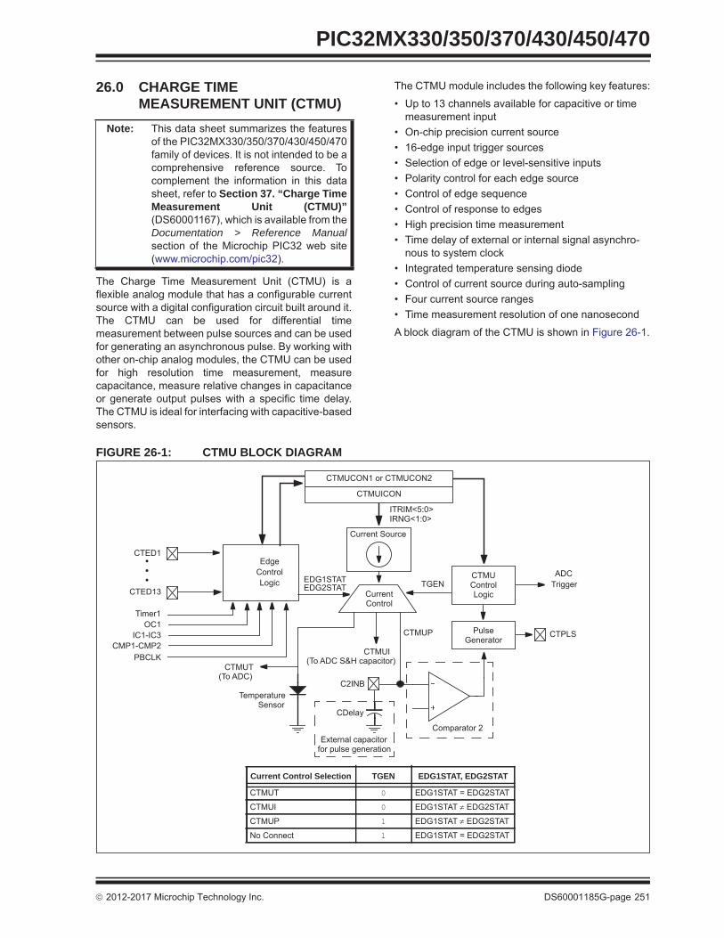
2012-2017 Microchip Technology Inc. DS60001185G-page 251
PIC32MX330/350/370/430/450/470
26.0 CHARGE TIME MEASUREMENT UNIT (CTMU)
Note: This data sheet summarizes the features of the PIC32MX330/350/370/430/450/470 family of devices. It is not intended to be a comprehensive reference source. To complement the information in this data sheet, refer to Section 37. “Charge Time Measurement Unit (CTMU)” (DS60001167), which is available from the Documentation > Reference Manual section of the Microchip PIC32 web site (www.microchip.com/pic32).
The Charge Time Measurement Unit (CTMU) is a flexible analog module that has a configurable current source with a digital configuration circuit built around it. The CTMU can be used for differential time measurement between pulse sources and can be used for generating an asynchronous pulse. By working with other on-chip analog modules, the CTMU can be used for high resolution time measurement, measure capacitance, measure relative changes in capacitance or generate output pulses with a specific time delay. The CTMU is ideal for interfacing with capacitive-based sensors.
The CTMU module includes the following key features:
• Up to 13 channels available for capacitive or time measurement input
• On-chip precision current source• 16-edge input trigger sources• Selection of edge or level-sensitive inputs• Polarity control for each edge source• Control of edge sequence• Control of response to edges• High precision time measurement• Time delay of external or internal signal asynchro-
nous to system clock• Integrated temperature sensing diode• Control of current source during auto-sampling• Four current source ranges• Time measurement resolution of one nanosecond
A block diagram of the CTMU is shown in Figure 26-1.
FIGURE 26-1: CTMU BLOCK DIAGRAM
CTED1
CTED13
Current Source
EdgeControlLogic
CTMUCON1 or CTMUCON2
PulseGenerator
CTMUI
Comparator 2
Timer1OC1
CurrentControl
ITRIM<5:0>IRNG<1:0>
CTMUICON
CTMUControlLogic
EDG1STATEDG2STAT
ADC
CTPLSIC1-IC3CMP1-CMP2
C2INB
CDelay
CTMUT
TemperatureSensor
Current Control Selection TGEN EDG1STAT, EDG2STAT
CTMUT 0 EDG1STAT = EDG2STAT
CTMUI 0 EDG1STAT EDG2STAT
CTMUP 1 EDG1STAT EDG2STAT
No Connect 1 EDG1STAT = EDG2STAT
TriggerTGEN
CTMUP
External capacitorfor pulse generation
(To ADC S&H capacitor)
(To ADC)
PBCLK
•••

PIC32M
X330/350/370/430/450/470
DS
60001185G-page
252
2012-2017 M
icrochip Technology Inc.
26.1 Control RegisterTABLE 26-1: CTMU REGISTER MAP
Virt
ual A
ddre
ss(B
F80_
#)
Reg
iste
rN
ame(1
)
Bit
Ran
ge
Bits
All
Res
ets
31/15 30/14 29/13 28/12 27/11 26/10 25/9 24/8 23/7 22/6 21/5 20/4 19/3 18/2 17/1 16/0
A200 CTMUCON31:16 EDG1MOD EDG1POL EDG1SEL<3:0> EDG2STAT EDG1STAT EDG2MOD EDG2POL EDG2SEL<3:0> — — 0000
15:0 ON — CTMUSIDL TGEN EDGEN EDGSEQEN IDISSEN CTTRIG ITRIM<5:0> IRNG<1:0> 0000Legend: x = unknown value on Reset; — = unimplemented, read as ‘0’. Reset values are shown in hexadecimal.Note 1: All registers in this table have corresponding CLR, SET and INV registers at its virtual address, plus an offset of 0x4, 0x8 and 0xC, respectively. See Section 12.2 “CLR, SET, and INV Registers” for
more information.

2012-2017 Microchip Technology Inc. DS60001185G-page 253
PIC32MX330/350/370/430/450/470
REGISTER 26-1: CTMUCON: CTMU CONTROL REGISTER Bit
RangeBit
31/23/15/7Bit
30/22/14/6Bit
29/21/13/5Bit
28/20/12/4Bit
27/19/11/3Bit
26/18/10/2Bit
25/17/9/1Bit
24/16/8/0
31:24 R/W-0 R/W-0 R/W-0 R/W-0 R/W-0 R/W-0 R/W-0 R/W-0EDG1MOD EDG1POL EDG1SEL<3:0> EDG2STAT EDG1STAT
23:16R/W-0 R/W-0 R/W-0 R/W-0 R/W-0 R/W-0 U-0 U-0
EDG2MOD EDG2POL EDG2SEL<3:0> — —
15:8R/W-0 U-0 R/W-0 R/W-0 R/W-0 R/W-0 R/W-0 R/W-0ON — CTMUSIDL TGEN(1) EDGEN EDGSEQEN IDISSEN(2) CTTRIG
7:0R/W-0 R/W-0 R/W-0 R/W-0 R/W-0 R/W-0 R/W-0 R/W-0
ITRIM<5:0> IRNG<1:0>
Legend:R = Readable bit W = Writable bit U = Unimplemented bit, read as ‘0’-n = Value at POR ‘1’ = Bit is set ‘0’ = Bit is cleared x = Bit is unknown
bit 31 EDG1MOD: Edge 1 Edge Sampling Select bit1 = Input is edge-sensitive0 = Input is level-sensitive
bit 30 EDG1POL: Edge 1 Polarity Select bit1 = Edge 1 programmed for a positive edge response0 = Edge 1 programmed for a negative edge response
bit 29-26 EDG1SEL<3:0>: Edge 1 Source Select bits1111 = Reserved1110 = C2OUT pin is selected1101 = C1OUT pin is selected1100 = IC3 Capture Event is selected1011 = IC2 Capture Event is selected1010 = IC1 Capture Event is selected1001 = CTED8 pin is selected1000 = CTED7 pin is selected0111 = CTED6 pin is selected0110 = CTED5 pin is selected0101 = CTED4 pin is selected0100 = CTED3 pin is selected0011 = CTED1 pin is selected0010 = CTED2 pin is selected0001 = OC1 Compare Event is selected0000 = Timer1 Event is selected
bit 25 EDG2STAT: Edge 2 Status bit Indicates the status of Edge 2 and can be written to control edge source1 = Edge 2 has occurred0 = Edge 2 has not occurred
Note 1: When this bit is set for Pulse Delay Generation, the EDG2SEL<3:0> bits must be set to ‘1110’ to select C2OUT.
2: The ADC module Sample and Hold capacitor is not automatically discharged between sample/conversion cycles. Software using the ADC as part of a capacitive measurement, must discharge the ADC capacitor before conducting the measurement. The IDISSEN bit, when set to ‘1’, performs this function. The ADC module must be sampling while the IDISSEN bit is active to connect the discharge sink to the capacitor array.
3: Refer to the CTMU Current Source Specifications (Table 31-42) in Section 31.0 “Electrical Characteristics” for current values.
4: This bit setting is not available for the CTMU temperature diode.

PIC32MX330/350/370/430/450/470
DS60001185G-page 254 2012-2017 Microchip Technology Inc.
bit 24 EDG1STAT: Edge 1 Status bit Indicates the status of Edge 1 and can be written to control edge source1 = Edge 1 has occurred0 = Edge 1 has not occurred
bit 23 EDG2MOD: Edge 2 Edge Sampling Select bit1 = Input is edge-sensitive0 = Input is level-sensitive
bit 22 EDG2POL: Edge 2 Polarity Select bit1 = Edge 2 programmed for a positive edge response0 = Edge 2 programmed for a negative edge response
bit 21-18 EDG2SEL<3:0>: Edge 2 Source Select bits1111 = Reserved1110 = C2OUT pin is selected1101 = C1OUT pin is selected1100 = PBCLK clock is selected1011 = IC3 Capture Event is selected1010 = IC2 Capture Event is selected1001 = IC1 Capture Event is selected1000 = CTED13 pin is selected0111 = CTED12 pin is selected0110 = CTED11 pin is selected0101 = CTED10 pin is selected0100 = CTED9 pin is selected0011 = CTED1 pin is selected0010 = CTED2 pin is selected0001 = OC1 Compare Event is selected0000 = Timer1 Event is selected
bit 17-16 Unimplemented: Read as ‘0’bit 15 ON: ON Enable bit
1 = Module is enabled0 = Module is disabled
bit 14 Unimplemented: Read as ‘0’bit 13 CTMUSIDL: Stop in Idle Mode bit
1 = Discontinue module operation when device enters Idle mode0 = Continue module operation in Idle mode
bit 12 TGEN: Time Generation Enable bit(1)
1 = Enables edge delay generation0 = Disables edge delay generation
bit 11 EDGEN: Edge Enable bit1 = Edges are not blocked0 = Edges are blocked
REGISTER 26-1: CTMUCON: CTMU CONTROL REGISTER (CONTINUED)
Note 1: When this bit is set for Pulse Delay Generation, the EDG2SEL<3:0> bits must be set to ‘1110’ to select C2OUT.
2: The ADC module Sample and Hold capacitor is not automatically discharged between sample/conversion cycles. Software using the ADC as part of a capacitive measurement, must discharge the ADC capacitor before conducting the measurement. The IDISSEN bit, when set to ‘1’, performs this function. The ADC module must be sampling while the IDISSEN bit is active to connect the discharge sink to the capacitor array.
3: Refer to the CTMU Current Source Specifications (Table 31-42) in Section 31.0 “Electrical Characteristics” for current values.
4: This bit setting is not available for the CTMU temperature diode.

2012-2017 Microchip Technology Inc. DS60001185G-page 255
PIC32MX330/350/370/430/450/470
bit 10 EDGSEQEN: Edge Sequence Enable bit1 = Edge 1 must occur before Edge 2 can occur0 = No edge sequence is needed
bit 9 IDISSEN: Analog Current Source Control bit(2)
1 = Analog current source output is grounded0 = Analog current source output is not grounded
bit 8 CTTRIG: Trigger Control bit 1 = Trigger output is enabled0 = Trigger output is disabled
bit 7-2 ITRIM<5:0>: Current Source Trim bits011111 = Maximum positive change from nominal current011110 •••000001 = Minimum positive change from nominal current000000 = Nominal current output specified by IRNG<1:0>111111 = Minimum negative change from nominal current•••100010 100001 = Maximum negative change from nominal current
bit 1-0 IRNG<1:0>: Current Range Select bits(3)
11 = 100 times base current10 = 10 times base current01 = Base current level00 = 1000 times base current(4)
REGISTER 26-1: CTMUCON: CTMU CONTROL REGISTER (CONTINUED)
Note 1: When this bit is set for Pulse Delay Generation, the EDG2SEL<3:0> bits must be set to ‘1110’ to select C2OUT.
2: The ADC module Sample and Hold capacitor is not automatically discharged between sample/conversion cycles. Software using the ADC as part of a capacitive measurement, must discharge the ADC capacitor before conducting the measurement. The IDISSEN bit, when set to ‘1’, performs this function. The ADC module must be sampling while the IDISSEN bit is active to connect the discharge sink to the capacitor array.
3: Refer to the CTMU Current Source Specifications (Table 31-42) in Section 31.0 “Electrical Characteristics” for current values.
4: This bit setting is not available for the CTMU temperature diode.

PIC32MX330/350/370/430/450/470
DS60001185G-page 256 2012-2017 Microchip Technology Inc.
NOTES:
2012-2017 Microchip Technology Inc. DS60001185G-page 257
PIC32MX330/350/370/430/450/47027.0 POWER-SAVING FEATURES
Note: This data sheet summarizes the features of the PIC32MX330/350/370/430/450/470 family of devices. It is not intended to be a comprehensive reference source. To complement the information in this data sheet, refer to Section 10. “Power-Saving Features” (DS60001130), whichis available from the Documentation > Reference Manual section of the Microchip PIC32 web site (www.microchip.com/pic32).
This section describes power-saving features for the PIC32MX330/350/370/430/450/470 family of devices. These PIC32 devices offer a total of nine methods and modes, organized into two categories, that allow the user to balance power consumption with device performance. In all of the methods and modes described in this section, power-saving is controlled by software.
27.1 Power Saving with CPU RunningWhen the CPU is running, power consumption can be controlled by reducing the CPU clock frequency, lowering the PBCLK and by individually disabling modules. These methods are grouped into the following categories:
• FRC Run mode: the CPU is clocked from the FRC clock source with or without postscalers.
• LPRC Run mode: the CPU is clocked from the LPRC clock source.
• SOSC Run mode: the CPU is clocked from the SOSC clock source.
In addition, the Peripheral Bus Scaling mode is available where peripherals are clocked at the programmable fraction of the CPU clock (SYSCLK).
27.2 CPU Halted MethodsThe device supports two power-saving modes, Sleep and Idle, both of which Halt the clock to the CPU. These modes operate with all clock sources, as listed below:
• POSC Idle mode: the system clock is derived from the POSC. The system clock source continues to operate. Peripherals continue to operate, but can optionally be individually disabled.
• FRC Idle mode: the system clock is derived from the FRC with or without postscalers. Peripherals continue to operate, but can optionally be individually disabled.
• SOSC Idle mode: the system clock is derived from the SOSC. Peripherals continue to operate, but can optionally be individually disabled.
• LPRC Idle mode: the system clock is derived from the LPRC. Peripherals continue to operate, but can optionally be individually disabled. This is the lowest power mode for the device with a clock
running.• Sleep mode: the CPU, the system clock source
and any peripherals that operate from the system clock source are Halted. Some peripherals can operate in Sleep using specific clock sources. This is the lowest power mode for the device.
27.3 Power-Saving OperationPeripherals and the CPU can be Halted or disabled to further reduce power consumption.
27.3.1 SLEEP MODESleep mode has the lowest power consumption of the device power-saving operating modes. The CPU and most peripherals are Halted. Select peripherals can continue to operate in Sleep mode and can be used to wake the device from Sleep. See the individual peripheral module sections for descriptions of behavior in Sleep.Sleep mode includes the following characteristics: • The CPU is Halted.• The system clock source is typically shutdown.
See Section 27.3.3 “Peripheral Bus Scaling Method” for specific information.
• There can be a wake-up delay based on the oscillator selection.
• The Fail-Safe Clock Monitor (FSCM) does not operate during Sleep mode.
• The BOR circuit remains operative during Sleep mode.
• The WDT, if enabled, is not automatically cleared prior to entering Sleep mode.
• Some peripherals can continue to operate at limited functionality in Sleep mode. These periph-erals include I/O pins that detect a change in the input signal, WDT, ADC, UART and peripherals that use an external clock input or the internal LPRC oscillator (e.g., RTCC, Timer1 and Input Capture).
• I/O pins continue to sink or source current in the same manner as they do when the device is not in Sleep.
• The USB module can override the disabling of the Posc or FRC. Refer to the USB section for specific details.
• Modules can be individually disabled by software prior to entering Sleep in order to further reduce consumption.

PIC32MX330/350/370/430/450/470
DS60001185G-page 258 2012-2017 Microchip Technology Inc.
The processor will exit, or ‘wake-up’, from Sleep on one of the following events:
• On any interrupt from an enabled source that is operating in Sleep. The interrupt priority must be greater than the current CPU priority.
• On any form of device Reset• On a WDT time-out
If the interrupt priority is lower than or equal to the current priority, the CPU will remain Halted, but the PBCLK will start running and the device will enter into Idle mode.
27.3.2 IDLE MODEIn Idle mode, the CPU is Halted but the System Clock (SYSCLK) source is still enabled. This allows peripher-als to continue operation when the CPU is Halted. Peripherals can be individually configured to Halt when entering Idle by setting their respective SIDL bit. Latency, when exiting Idle mode, is very low due to the CPU oscillator source remaining active.
Note 1: Changing the PBCLK divider ratio requires recalculation of peripheral tim-ing. For example, assume the UART is configured for 9600 baud with a PB clock ratio of 1:1 and a POSC of 8 MHz. When the PB clock divisor of 1:2 is used, the input frequency to the baud clock is cut in half; therefore, the baud rate is reduced to 1/2 its former value. Due to numeric truncation in calculations (such as the baud rate divisor), the actual baud rate may be a tiny percentage different than expected. For this reason, any timing cal-culation required for a peripheral should be performed with the new PB clock fre-quency instead of scaling the previous value based on a change in the PB divisor ratio.
2: Oscillator start-up and PLL lock delays are applied when switching to a clock source that was disabled and that uses a crystal and/or the PLL. For example, assume the clock source is switched from POSC to LPRC just prior to entering Sleep in order to save power. No oscillator start-up delay would be applied when exiting Idle. However, when switching back to POSC, the appropriate PLL and/or oscillator start-up/lock delays would be applied.
The device enters Idle mode when the SLPEN bit (OSCCON<4>) is clear and a WAIT instruction is executed.
The processor will wake or exit from Idle mode on the following events:
• On any interrupt event for which the interrupt source is enabled. The priority of the interrupt event must be greater than the current priority of the CPU. If the priority of the interrupt event is lower than or equal to current priority of the CPU, the CPU will remain Halted and the device will remain in Idle mode.
• On any form of device Reset• On a WDT time-out interrupt
27.3.3 PERIPHERAL BUS SCALING METHOD
Most of the peripherals on the device are clocked using the PBCLK. The peripheral bus can be scaled relative to the SYSCLK to minimize the dynamic power consumed by the peripherals. The PBCLK divisor is controlled by PBDIV<1:0> (OSCCON<20:19>), allowing SYSCLK to PBCLK ratios of 1:1, 1:2, 1:4 and 1:8. All peripherals using PBCLK are affected when the divisor is changed. Peripherals such as the USB, Interrupt Controller, DMA, and the bus matrix are clocked directly from SYSCLK. As a result, they are not affected by PBCLK divisor changes.
Changing the PBCLK divisor affects:
• The CPU to peripheral access latency. The CPU has to wait for next PBCLK edge for a read to complete. In 1:8 mode, this results in a latency of one to seven SYSCLKs.
• The power consumption of the peripherals. Power consumption is directly proportional to the frequency at which the peripherals are clocked. The greater the divisor, the lower the power consumed by the peripherals.
To minimize dynamic power, the PB divisor should be chosen to run the peripherals at the lowest frequency that provides acceptable system performance. When selecting a PBCLK divider, peripheral clock require-ments, such as baud rate accuracy, should be taken into account. For example, the UART peripheral may not be able to achieve all baud rate values at some PBCLK divider depending on the SYSCLK value.

2012-2017 Microchip Technology Inc. DS60001185G-page 259
PIC32MX330/350/370/430/450/47027.4 Peripheral Module DisableThe Peripheral Module Disable (PMD) registers provide a method to disable a peripheral module by stopping all clock sources supplied to that module. When a peripheral is disabled using the appropriate PMD control bit, the peripheral is in a minimum power consumption state. The control and status registers associated with the peripheral are also disabled, so writes to those registers do not have effect and read values are invalid.
To disable a peripheral, the associated PMDx bit must be set to ‘1’. To enable a peripheral, the associated PMDx bit must be cleared (default). See Table 27-1 for more information.
Note: Disabling a peripheral module while it’s ON bit is set, may result in undefined behavior. The ON bit for the associated peripheral module must be cleared prior to disable a module via the PMDx bits.
TABLE 27-1: PERIPHERAL MODULE DISABLE BITS AND LOCATIONSPeripheral(1) PMDx bit Name(1) Register Name and Bit Location
ADC1 AD1MD PMD1<0>CTMU CTMUMD PMD1<8>Comparator Voltage Reference CVRMD PMD1<12>Comparator 1 CMP1MD PMD2<0>Comparator 2 CMP2MD PMD2<1>Input Capture 1 IC1MD PMD3<0>Input Capture 2 IC2MD PMD3<1>Input Capture 3 IC3MD PMD3<2>Input Capture 4 IC4MD PMD3<3>Input Capture 5 IC5MD PMD3<4>Output Compare 1 OC1MD PMD3<16>Output Compare 2 OC2MD PMD3<17>Output Compare 3 OC3MD PMD3<18>Output Compare 4 OC4MD PMD3<19>Output Compare 5 OC5MD PMD3<20>Timer1 T1MD PMD4<0>Timer2 T2MD PMD4<1>Timer3 T3MD PMD4<2>Timer4 T4MD PMD4<3>Timer5 T5MD PMD4<4>UART1 U1MD PMD5<0>UART2 U2MD PMD5<1>UART3 U3MD PMD5<2>UART4 U4MD PMD5<3>UART5 U5MD PMD5<4>SPI1 SPI1MD PMD5<8>SPI2 SPI2MD PMD5<9>I2C1 I2C1MD PMD5<16>I2C2 I2C2MD PMD5<17>USB(2) USBMD PMD5<24>RTCC RTCCMD PMD6<0>Reference Clock Output REFOMD PMD6<1>PMP PMPMD PMD6<16>Note 1: Not all modules and associated PMDx bits are available on all devices. See TABLE 1: “PIC32MX330/
350/370/430/450/470 Controller Family Features” for the lists of available peripherals.2: Module must not be busy after clearing the associated ON bit and prior to setting the USBMD bit.

PIC32MX330/350/370/430/450/470
DS60001185G-page 260 2012-2017 Microchip Technology Inc.
27.4.1 CONTROLLING CONFIGURATION CHANGES
Because peripherals can be disabled during run time, some restrictions on disabling peripherals are needed to prevent accidental configuration changes. PIC32devices include two features to prevent alterations to enabled or disabled peripherals:
• Control register lock sequence• Configuration bit select lock
27.4.1.1 Control Register LockUnder normal operation, writes to the PMDx registers are not allowed. Attempted writes appear to execute normally, but the contents of the registers remain unchanged. To change these registers, they must be unlocked in hardware. The register lock is controlled by the PMDLOCK Configuration bit (CFGCON<12>). Set-ting PMDLOCK prevents writes to the control registers; clearing PMDLOCK allows writes.
To set or clear PMDLOCK, an unlock sequence must be executed. Refer to Section 6. “Oscillator”(DS60001112) in the “PIC32 Family Reference Manual” for details.
27.4.1.2 Configuration Bit Select LockAs an additional level of safety, the device can be configured to prevent more than one write session to the PMDx registers. The PMDL1WAY Configuration bit (DEVCFG3<28>) blocks the PMDLOCK bit from being cleared after it has been set once. If PMDLOCK remains set, the register unlock procedure does not execute, and the peripheral pin select control registers cannot be written to. The only way to clear the bit and re-enable PMD functionality is to perform a device Reset.

2012-2017 Microchip Technology Inc. DS60001185G-page 261
PIC32MX330/350/370/430/450/47028.0 SPECIAL FEATURES
Note: This data sheet summarizes the features of the PIC32MX330/350/370/430/450/470 family of devices. However, it is not intended to be a comprehensive reference source. To complement the information in this data sheet, refer toSection 32. “Configuration”(DS60001124) and Section 33. “Programming and Diagnostics”(DS60001129), which are available from the Documentation > Reference Manual section of the Microchip PIC32 web site (www.microchip.com/pic32).
The PIC32MX330/350/370/430/450/470 family of devices include several features intended to maximize application flexibility and reliability and minimize cost through elimination of external components. These are:• Flexible device configuration• Joint Test Action Group (JTAG) interface• In-Circuit Serial Programming™ (ICSP™)
28.1 Configuration BitsThe Configuration bits can be programmed using the following registers to select various device configurations.
• DEVCFG0: Device Configuration Word 0• DEVCFG1: Device Configuration Word 1• DEVCFG2: Device Configuration Word 2• DEVCFG3: Device Configuration Word 3• CFGCON: Configuration Control Register
In addition, the DEVID register (Register 28-6) provides device and revision information.

TABLE 28-2: DEVICE ID, REVISION, AND CONFIGURATION SUMMARY
Virt
ual A
ddre
ss(B
F80_
#)
Reg
iste
rN
ame
Bit
Ran
ge
Bits
All
Res
ets
31/15 30/14 29/13 28/12 27/11 26/10 25/9 24/8 23/7 22/6 21/5 20/4 19/3 18/2 17/1 16/0
F200 CFGCON31:16 — — — — — — — — — — — — — — — — 0000
15:0 — — IOLOCK PMDLOCK — — — — — — — — JTAGEN TROEN — TDOEN 000B
F220 DEVID31:16 VER<3:0> DEVID<27:16> xxxx(1)15:0 DEVID<15:0> xxxx(1)
F230 SYSKEY31:16
SYSKEY<31:0>0000
15:0 0000Legend: x = unknown value on Reset; — = unimplemented, read as ‘0’. Reset values are shown in hexadecimal.Note 1: Reset values are dependent on the device variant.
PIC32M
X330/350/370/430/450/470
DS
60001185G-page
262
2012-2017 M
icrochip Technology Inc.
TABLE 28-1: DEVCFG: DEVICE CONFIGURATION WORD SUMMARY Vi
rtua
l Add
ress
(BFC
0_#)
Reg
iste
rN
ame
Bit
Ran
ge
Bits
All
Res
ets
31/15 30/14 29/13 28/12 27/11 26/10 25/9 24/8 23/7 22/6 21/5 20/4 19/3 18/2 17/1 16/0
2FF0 DEVCFG331:16 FVBUSONIO FUSBIDIO IOL1WAY PMDL1WAY — — — — — — — — — FSRSSEL<2:0> xxxx15:0 USERID<15:0> xxxx
2FF4 DEVCFG231:16 — — — — — — — — — — — — — FPLLODIV<2:0> xxxx15:0 UPLLEN(1) — — — — UPLLIDIV<2:0>(1) — FPLLMUL<2:0> — FPLLIDIV<2:0> xxxx
2FF8 DEVCFG131:16 — — — — — — FWDTWINSZ<1:0> FWDTEN WINDIS — WDTPS<4:0> xxxx15:0 FCKSM<1:0> FPBDIV<1:0> — OSCIOFNC POSCMOD<1:0> IESO — FSOSCEN — — FNOSC<2:0> xxxx
2FFC DEVCFG031:16 — — — CP — — — BWP — — — — PWP<7:4> xxxx15:0 PWP<3:0> — — — — — — — ICESEL<1:0> JTAGEN DEBUG<1:0> xxxx
Legend: x = unknown value on Reset; — = reserved, write as ‘1’. Reset values are shown in hexadecimal.Note 1: This bit is only available on devices with a USB module.

2012-2017 Microchip Technology Inc. DS60001185G-page 263
PIC32MX330/350/370/430/450/470
REGISTER 28-1: DEVCFG0: DEVICE CONFIGURATION WORD 0 Bit
RangeBit
31/23/15/7Bit
30/22/14/6Bit
29/21/13/5Bit
28/20/12/4Bit
27/19/11/3Bit
26/18/10/2Bit
25/17/9/1Bit
24/16/8/0
31:24r-0 r-1 r-1 R/P r-1 r-1 r-1 R/P
— — — CP — — — BWP
23:16r-1 r-1 r-1 r-1 R/P R/P R/P R/P
— — — — PWP<7:4>
15:8R/P R/P R/P R/P r-1 r-1 r-1 r-1
PWP<3:0> — — — —
7:0r-1 r-1 r-1 R/P R/P R/P R/P R/P
— — — ICESEL<1:0> JTAGEN(1) DEBUG<1:0>
Legend: r = Reserved bit P = Programmable bitR = Readable bit W = Writable bit U = Unimplemented bit, read as ‘0’-n = Value at POR ‘1’ = Bit is set ‘0’ = Bit is cleared x = Bit is unknown
bit 31 Reserved: Write ‘0’bit 30-29 Reserved: Write ‘1’bit 28 CP: Code-Protect bit
Prevents boot and program Flash memory from being read or modified by an external pro-gramming device.1 = Protection is disabled0 = Protection is enabled
bit 27-25 Reserved: Write ‘1’bit 24 BWP: Boot Flash Write-Protect bit
Prevents boot Flash memory from being modified during code execution.1 = Boot Flash is writable0 = Boot Flash is not writable
bit 23-20 Reserved: Write ‘1’bit 19-12 PWP<7:0>: Program Flash Write-Protect bits
Prevents selected program Flash memory pages from being modified during code execution. The PWP bits represent the one’s compliment of the number of write protected program Flash memory pages. 11111111 = Disabled11111110 = 0xBD00_0FFF11111101 = 0xBD00_1FFF11111100 = 0xBD00_2FFF11111011 = 0xBD00_3FFF11111010 = 0xBD00_4FFF11111001 = 0xBD00_5FFF11111000 = 0xBD00_6FFF11110111 = 0xBD00_7FFF11110110 = 0xBD00_8FFF11110101 = 0xBD00_9FFF11110100 = 0xBD00_AFFF11110011 = 0xBD00_BFFF11110010 = 0xBD00_CFFF11110001 = 0xBD00_DFFF11110000 = 0xBD00_EFFF11101111 = 0xBD00_FFFF...01111111 = 0xBD07_FFFF
Note 1: This bit sets the value for the JTAGEN bit in the CFGCON register.

PIC32MX330/350/370/430/450/470
DS60001185G-page 264 2012-2017 Microchip Technology Inc.
bit 11-5 Reserved: Write ‘1’bit 4-3 ICESEL<1:0>: In-Circuit Emulator/Debugger Communication Channel Select bits
11 = PGEC1/PGED1 pair is used10 = PGEC2/PGED2 pair is used01 = PGEC3/PGED3 pair is used00 = Reserved
bit 2 JTAGEN: JTAG Enable bit(1)
1 = JTAG is enabled0 = JTAG is disabled
bit 1-0 DEBUG<1:0>: Background Debugger Enable bits (forced to ‘11’ if code-protect is enabled)1x = Debugger is disabled0x = Debugger is enabled
REGISTER 28-1: DEVCFG0: DEVICE CONFIGURATION WORD 0 (CONTINUED)
Note 1: This bit sets the value for the JTAGEN bit in the CFGCON register.

2012-2017 Microchip Technology Inc. DS60001185G-page 265
PIC32MX330/350/370/430/450/470 REGISTER 28-2: DEVCFG1: DEVICE CONFIGURATION WORD 1
Bit Range
Bit31/23/15/7
Bit30/22/14/6
Bit29/21/13/5
Bit28/20/12/4
Bit27/19/11/3
Bit26/18/10/2
Bit25/17/9/1
Bit24/16/8/0
31:24r-1 r-1 r-1 r-1 r-1 r-1 R/P R/P
— — — — — — FWDTWINSZ<1:0>
23:16R/P R/P r-1 R/P R/P R/P R/P R/P
FWDTEN WINDIS — WDTPS<4:0>
15:8R/P R/P R/P R/P r-1 R/P R/P R/P
FCKSM<1:0> FPBDIV<1:0> — OSCIOFNC POSCMOD<1:0>
7:0R/P r-1 R/P r-1 r-1 R/P R/P R/P
IESO — FSOSCEN — — FNOSC<2:0>
Legend: r = Reserved bit P = Programmable bitR = Readable bit W = Writable bit U = Unimplemented bit, read as ‘0’-n = Value at POR ‘1’ = Bit is set ‘0’ = Bit is cleared x = Bit is unknown
bit 31-26 Reserved: Write ‘1’bit 25-24 FWDTWINSZ<1:0>: Watchdog Timer Window Size bits
11 = Window size is 25%10 = Window size is 37.5%01 = Window size is 50%00 = Window size is 75%
bit 23 FWDTEN: Watchdog Timer Enable bit1 = Watchdog Timer is enabled and cannot be disabled by software0 = Watchdog Timer is not enabled; it can be enabled in software
bit 22 WINDIS: Watchdog Timer Window Enable bit1 = Watchdog Timer is in non-Window mode0 = Watchdog Timer is in Window mode
bit 21 Reserved: Write ‘1’bit 20-16 WDTPS<4:0>: Watchdog Timer Postscale Select bits
10100 = 1:104857610011 = 1:52428810010 = 1:26214410001 = 1:13107210000 = 1:6553601111 = 1:3276801110 = 1:1638401101 = 1:819201100 = 1:409601011 = 1:204801010 = 1:102401001 = 1:51201000 = 1:25600111 = 1:12800110 = 1:6400101 = 1:3200100 = 1:1600011 = 1:800010 = 1:400001 = 1:200000 = 1:1All other combinations not shown result in operation = 10100
Note 1: Do not disable the POSC (POSCMOD = 11) when using this oscillator source.

PIC32MX330/350/370/430/450/470
DS60001185G-page 266 2012-2017 Microchip Technology Inc.
bit 15-14 FCKSM<1:0>: Clock Switching and Monitor Selection Configuration bits1x = Clock switching is disabled, Fail-Safe Clock Monitor is disabled01 = Clock switching is enabled, Fail-Safe Clock Monitor is disabled00 = Clock switching is enabled, Fail-Safe Clock Monitor is enabled
bit 13-12 FPBDIV<1:0>: Peripheral Bus Clock Divisor Default Value bits11 = PBCLK is SYSCLK divided by 810 = PBCLK is SYSCLK divided by 401 = PBCLK is SYSCLK divided by 200 = PBCLK is SYSCLK divided by 1
bit 11 Reserved: Write ‘1’bit 10 OSCIOFNC: CLKO Enable Configuration bit
1 = CLKO output is disabled0 = CLKO output signal active on the OSCO pin; Primary Oscillator must be disabled or configured for the
External Clock mode (EC) for the CLKO to be active (POSCMOD<1:0> = 11 or 00)bit 9-8 POSCMOD<1:0>: Primary Oscillator Configuration bits
11 = Primary Oscillator is disabled10 = HS Oscillator mode is selected01 = XT Oscillator mode is selected00 = External Clock mode is selected
bit 7 IESO: Internal External Switchover bit1 = Internal External Switchover mode is enabled (Two-Speed Start-up is enabled)0 = Internal External Switchover mode is disabled (Two-Speed Start-up is disabled)
bit 6 Reserved: Write ‘1’bit 5 FSOSCEN: Secondary Oscillator Enable bit
1 = Enable Secondary Oscillator0 = Disable Secondary Oscillator
bit 4-3 Reserved: Write ‘1’bit 2-0 FNOSC<2:0>: Oscillator Selection bits
111 = Fast RC Oscillator with divide-by-N (FRCDIV)110 = FRCDIV16 Fast RC Oscillator with fixed divide-by-16 postscaler101 = Low-Power RC Oscillator (LPRC)100 = Secondary Oscillator (SOSC)011 = Primary Oscillator (POSC) with PLL module (XT+PLL, HS+PLL, EC+PLL) 010 = Primary Oscillator (XT, HS, EC)(1)
001 = Fast RC Oscillator with divide-by-N with PLL module (FRCDIV+PLL)000 = Fast RC Oscillator (FRC)
REGISTER 28-2: DEVCFG1: DEVICE CONFIGURATION WORD 1 (CONTINUED)
Note 1: Do not disable the POSC (POSCMOD = 11) when using this oscillator source.

2012-2017 Microchip Technology Inc. DS60001185G-page 267
PIC32MX330/350/370/430/450/470
REGISTER 28-3: DEVCFG2: DEVICE CONFIGURATION WORD 2 Bit
RangeBit
31/23/15/7Bit
30/22/14/6Bit
29/21/13/5Bit
28/20/12/4Bit
27/19/11/3Bit
26/18/10/2Bit
25/17/9/1Bit
24/16/8/0
31:24r-1 r-1 r-1 r-1 r-1 r-1 r-1 r-1
— — — — — — — —
23:16r-1 r-1 r-1 r-1 r-1 R/P R/P R/P
— — — — — FPLLODIV<2:0>
15:8R/P r-1 r-1 r-1 r-1 R/P R/P R/P
UPLLEN(1) — — — — UPLLIDIV<2:0>(1)
7:0r-1 R/P-1 R/P R/P-1 r-1 R/P R/P R/P
— FPLLMUL<2:0> — FPLLIDIV<2:0>
Legend: r = Reserved bit P = Programmable bitR = Readable bit W = Writable bit U = Unimplemented bit, read as ‘0’-n = Value at POR ‘1’ = Bit is set ‘0’ = Bit is cleared x = Bit is unknown
bit 31-19 Reserved: Write ‘1’bit 18-16 FPLLODIV<2:0>: Default PLL Output Divisor bits
111 = PLL output divided by 256110 = PLL output divided by 64101 = PLL output divided by 32100 = PLL output divided by 16011 = PLL output divided by 8010 = PLL output divided by 4001 = PLL output divided by 2000 = PLL output divided by 1
bit 15 UPLLEN: USB PLL Enable bit(1)
1 = Disable and bypass USB PLL0 = Enable USB PLL
bit 14-11 Reserved: Write ‘1’bit 10-8 UPLLIDIV<2:0>: USB PLL Input Divider bits(1)
111 = 12x divider110 = 10x divider101 = 6x divider100 = 5x divider011 = 4x divider010 = 3x divider001 = 2x divider000 = 1x divider
bit 7 Reserved: Write ‘1’bit 6-4 FPLLMUL<2:0>: PLL Multiplier bits
111 = 24x multiplier110 = 21x multiplier101 = 20x multiplier100 = 19x multiplier011 = 18x multiplier010 = 17x multiplier001 = 16x multiplier000 = 15x multiplier
bit 3 Reserved: Write ‘1’
Note 1: This bit is available on PIC32MX4XX devices only.

PIC32MX330/350/370/430/450/470
DS60001185G-page 268 2012-2017 Microchip Technology Inc.
bit 2-0 FPLLIDIV<2:0>: PLL Input Divider bits111 = 12x divider110 = 10x divider101 = 6x divider100 = 5x divider011 = 4x divider010 = 3x divider001 = 2x divider000 = 1x divider
REGISTER 28-3: DEVCFG2: DEVICE CONFIGURATION WORD 2 (CONTINUED)
Note 1: This bit is available on PIC32MX4XX devices only.

2012-2017 Microchip Technology Inc. DS60001185G-page 269
PIC32MX330/350/370/430/450/470
REGISTER 28-4: DEVCFG3: DEVICE CONFIGURATION WORD 3 Bit
RangeBit
31/23/15/7Bit
30/22/14/6Bit
29/21/13/5Bit
28/20/12/4Bit
27/19/11/3Bit
26/18/10/2Bit
25/17/9/1Bit
24/16/8/0
31:24R/P R/P R/P R/P U-0 U-0 U-0 U-0
FVBUSONIO FUSBIDIO IOL1WAY PMDL1WAY — — — —
23:16U-0 U-0 U-0 U-0 U-0 R/P R/P R/P
— — — — — FSRSSEL<2:0>
15:8R/P R/P R/P R/P R/P R/P R/P R/P
USERID<15:8>
7:0R/P R/P R/P R/P R/P R/P R/P R/P
USERID<7:0>
Legend: r = Reserved bit P = Programmable bitR = Readable bit W = Writable bit U = Unimplemented bit, read as ‘0’-n = Value at POR ‘1’ = Bit is set ‘0’ = Bit is cleared x = Bit is unknown
bit 31 FVBUSONIO: USB VBUS_ON Selection bit1 = VBUSON pin is controlled by the USB module0 = VBUSON pin is controlled by the port function
bit 30 FUSBIDIO: USB USBID Selection bit1 = USBID pin is controlled by the USB module0 = USBID pin is controlled by the port function
bit 29 IOL1WAY: Peripheral Pin Select Configuration bit1 = Allow only one reconfiguration0 = Allow multiple reconfigurations
bit 28 PMDL1WAY: Peripheral Module Disable Configuration bit1 = Allow only one reconfiguration0 = Allow multiple reconfigurations
bit 27-19 Unimplemented: Read as ‘0’bit 18-16 FSRSSEL<2:0>: Shadow Register Set Priority Select bit
These bits assign an interrupt priority to a shadow register.111 = Shadow register set used with interrupt priority 7110 = Shadow register set used with interrupt priority 6101 = Shadow register set used with interrupt priority 5100 = Shadow register set used with interrupt priority 4011 = Shadow register set used with interrupt priority 3010 = Shadow register set used with interrupt priority 2001 = Shadow register set used with interrupt priority 1000 = Shadow register set used with interrupt priority 0
bit 15-0 USERID<15:0>: This is a 16-bit value that is user-defined and is readable via ICSP™ and JTAG

PIC32MX330/350/370/430/450/470
DS60001185G-page 270 2012-2017 Microchip Technology Inc.
REGISTER 28-5: CFGCON: CONFIGURATION CONTROL REGISTER Bit
RangeBit
31/23/15/7Bit
30/22/14/6Bit
29/21/13/5Bit
28/20/12/4Bit
27/19/11/3Bit
26/18/10/2Bit
25/17/9/1Bit
24/16/8/0
31:24U-0 U-0 U-0 U-0 U-0 U-0 U-0 U-0
— — — — — — — —
23:16U-0 U-0 U-0 U-0 U-0 U-0 U-0 U-0
— — — — — — — —
15:8U-0 U-0 R/W-0 R/W-0 U-0 U-0 U-0 U-0
— — IOLOCK(1) PMDLOCK(1) — — — —
7:0U-0 U-0 U-0 U-0 R/W-0 R/W-0 U-0 R/W-1
— — — — JTAGEN TROEN — TDOEN
Legend:R = Readable bit W = Writable bit U = Unimplemented bit, read as ‘0’-n = Value at POR ‘1’ = Bit is set ‘0’ = Bit is cleared x = Bit is unknown
bit 31-14 Unimplemented: Read as ‘0’bit 13 IOLOCK: Peripheral Pin Select Lock bit(1)
1 = Peripheral Pin Select is locked. Writes to PPS registers is not allowed0 = Peripheral Pin Select is not locked. Writes to PPS registers is allowed
bit 12 PMDLOCK: Peripheral Module Disable bit(1)
1 = Peripheral module is locked. Writes to PMD registers is not allowed0 = Peripheral module is not locked. Writes to PMD registers is allowed
bit 11-4 Unimplemented: Read as ‘0’bit 3 JTAGEN: JTAG Port Enable bit
1 = Enable the JTAG port0 = Disable the JTAG port
bit 2 TROEN: Trace Output Enable bit1 = Enable trace outputs and start trace clock (trace probe must be present)0 = Disable trace outputs and stop trace clock
bit 1 Unimplemented: Read as ‘0’bit 0 TDOEN: TDO Enable for 2-Wire JTAG
1 = 2-wire JTAG protocol uses TDO0 = 2-wire JTAG protocol does not use TDO
Note 1: To change this bit, the unlock sequence must be performed. Refer to Section 6. “Oscillator” (DS60001112) in the “PIC32 Family Reference Manual” for details.

2012-2017 Microchip Technology Inc. DS60001185G-page 271
PIC32MX330/350/370/430/450/470
REGISTER 28-6: DEVID: DEVICE AND REVISION ID REGISTER Bit
RangeBit
31/23/15/7Bit
30/22/14/6Bit
29/21/13/5Bit
28/20/12/4Bit
27/19/11/3Bit
26/18/10/2Bit
25/17/9/1Bit
24/16/8/0
31:24R R R R R R R R
VER<3:0>(1) DEVID<27:24>(1)
23:16R R R R R R R R
DEVID<23:16>(1)
15:8R R R R R R R R
DEVID<15:8>(1)
7:0R R R R R R R R
DEVID<7:0>(1)
Legend:R = Readable bit W = Writable bit U = Unimplemented bit, read as ‘0’-n = Value at POR ‘1’ = Bit is set ‘0’ = Bit is cleared x = Bit is unknown
bit 31-28 VER<3:0>: Revision Identifier bits(1)
bit 27-0 DEVID<27:0>: Device ID(1)
Note 1: See the “PIC32 Flash Programming Specification” (DS60001145) for a list of Revision and Device ID values.

PIC32MX330/350/370/430/450/470
DS60001185G-page 272 2012-2017 Microchip Technology Inc.
28.2 On-Chip Voltage RegulatorAll PIC32MX330/350/370/430/450/470 devices’ core and digital logic are designed to operate at a nominal 1.8V. To simplify system designs, most devices in the PIC32MX330/350/370/430/450/470 family incorporate an on-chip regulator providing the required core logic voltage from VDD.A low-ESR capacitor (such as tantalum) must be connected to the VCAP pin (see Figure 28-1). This helps to maintain the stability of the regulator. The recommended value for the filter capacitor is provided in Section 31.1 “DC Characteristics”.
Note: It is important that the low-ESR capacitor is placed as close as possible to the VCAPpin.
28.2.1 HIGH VOLTAGE DETECT (HVD)The HVD module monitors the core voltage at the VCAPpin. If a voltage above the required level is detected on VCAP, the I/O pins are disabled and the device is held in Reset as long as the HVD condition persists. See parameter HV10 (VHVD) in Table 31-11 in Section 31.1 “DC Characteristics” for more information.
28.2.2 ON-CHIP REGULATOR AND PORIt takes a fixed delay for the on-chip regulator to generate an output. During this time, designated as TPU, code execution is disabled. TPU is applied every time the device resumes operation after any power-down, including Sleep mode.
28.2.3 ON-CHIP REGULATOR AND BORPIC32MX330/350/370/430/450/470 devices also have a simple brown-out capability. If the voltage supplied to the regulator is inadequate to maintain a regulated level, the regulator Reset circuitry will generate a Brown-out Reset. This event is captured by the BORflag bit (RCON<1>). The brown-out voltage levels are specific in Section 31.1 “DC Characteristics”.
FIGURE 28-1: CONNECTIONS FOR THE ON-CHIP REGULATOR
VDD
VCAP
VSS
PIC32
CEFC(2,3)
3.3V(1)
Note 1: These are typical operating voltages. Refer to Section 31.1 “DC Characteristics” for the full operating ranges of VDD.
2: It is important that the low-ESR capacitor is placed as close as possible to the VCAP pin.
3: The typical voltage on the VCAP pin is 1.8V.
(10 F typ)
28.3 Programming and DiagnosticsPIC32MX330/350/370/430/450/470 devices provide a complete range of programming and diagnostic fea-tures that can increase the flexibility of any application using them. These features allow system designers to include:• Simplified field programmability using two-wire
In-Circuit Serial Programming™ (ICSP™) interfaces
• Debugging using ICSP• Programming and debugging capabilities using
the EJTAG extension of JTAG• JTAG boundary scan testing for device and board
diagnosticsPIC32 devices incorporate two programming and diag-nostic modules, and a trace controller, that provide a range of functions to the application developer.
FIGURE 28-2: BLOCK DIAGRAM OF PROGRAMMING, DEBUGGING AND TRACE PORTS
TDI
TDO
TCK
TMS
JTAGController
ICSP™Controller
Core
JTAGEN DEBUG<1:0>
ICESEL
PGEC1
PGED1
PGEC3
PGED3
Instruction TraceController
DEBUG<1:0>
TRCLK
TRD0
TRD2
TRD3
TRD1

2012-2017 Microchip Technology Inc. DS60001185G-page 273
PIC32MX330/350/370/430/450/47029.0 INSTRUCTION SETThe PIC32MX330/350/370/430/450/470 family instruction set complies with the MIPS32® Release 2 instruction set architecture. The PIC32 device family does not support the following features:
• Core extend instructions • Coprocessor 1 instructions• Coprocessor 2 instructions
Note: Refer to “MIPS32® Architecture for Programmers Volume II: The MIPS32®
Instruction Set” at www.imgtec.com for more information.

PIC32MX330/350/370/430/450/470
DS60001185G-page 274 2012-2017 Microchip Technology Inc.
NOTES:

2012-2017 Microchip Technology Inc. DS60001185G-page 275
PIC32MX330/350/370/430/450/47030.0 DEVELOPMENT SUPPORTThe PIC® microcontrollers (MCU) and dsPIC® digital signal controllers (DSC) are supported with a full range of software and hardware development tools:
• Integrated Development Environment- MPLAB® X IDE Software
• Compilers/Assemblers/Linkers- MPLAB XC Compiler - MPASMTM Assembler- MPLINKTM Object Linker/
MPLIBTM Object Librarian- MPLAB Assembler/Linker/Librarian for
Various Device Families• Simulators
- MPLAB X SIM Software Simulator• Emulators
- MPLAB REAL ICE™ In-Circuit Emulator• In-Circuit Debuggers/Programmers
- MPLAB ICD 3- PICkit™ 3
• Device Programmers- MPLAB PM3 Device Programmer
• Low-Cost Demonstration/Development Boards, Evaluation Kits and Starter Kits
• Third-party development tools
30.1 MPLAB X Integrated Development Environment Software
The MPLAB X IDE is a single, unified graphical user interface for Microchip and third-party software, and hardware development tool that runs on Windows®, Linux and Mac OS® X. Based on the NetBeans IDE, MPLAB X IDE is an entirely new IDE with a host of free software components and plug-ins for high-performance application development and debugging. Moving between tools and upgrading from software simulators to hardware debugging and programming tools is simple with the seamless user interface.
With complete project management, visual call graphs, a configurable watch window and a feature-rich editor that includes code completion and context menus, MPLAB X IDE is flexible and friendly enough for new users. With the ability to support multiple tools on multiple projects with simultaneous debugging, MPLAB X IDE is also suitable for the needs of experienced users.
Feature-Rich Editor:
• Color syntax highlighting• Smart code completion makes suggestions and
provides hints as you type• Automatic code formatting based on user-defined
rules• Live parsing
User-Friendly, Customizable Interface:
• Fully customizable interface: toolbars, toolbar buttons, windows, window placement, etc.
• Call graph window
Project-Based Workspaces:
• Multiple projects• Multiple tools• Multiple configurations• Simultaneous debugging sessions
File History and Bug Tracking:
• Local file history feature• Built-in support for Bugzilla issue tracker

PIC32MX330/350/370/430/450/470
DS60001185G-page 276 2012-2017 Microchip Technology Inc.
30.2 MPLAB XC CompilersThe MPLAB XC Compilers are complete ANSI C compilers for all of Microchip’s 8, 16, and 32-bit MCU and DSC devices. These compilers provide powerful integration capabilities, superior code optimization and ease of use. MPLAB XC Compilers run on Windows, Linux or MAC OS X.
For easy source level debugging, the compilers provide debug information that is optimized to the MPLAB X IDE.
The free MPLAB XC Compiler editions support all devices and commands, with no time or memory restrictions, and offer sufficient code optimization for most applications.
MPLAB XC Compilers include an assembler, linker and utilities. The assembler generates relocatable object files that can then be archived or linked with other relo-catable object files and archives to create an execut-able file. MPLAB XC Compiler uses the assembler to produce its object file. Notable features of the assem-bler include:
• Support for the entire device instruction set• Support for fixed-point and floating-point data• Command-line interface• Rich directive set• Flexible macro language• MPLAB X IDE compatibility
30.3 MPASM AssemblerThe MPASM Assembler is a full-featured, universal macro assembler for PIC10/12/16/18 MCUs.
The MPASM Assembler generates relocatable object files for the MPLINK Object Linker, Intel® standard HEX files, MAP files to detail memory usage and symbol reference, absolute LST files that contain source lines and generated machine code, and COFF files for debugging.
The MPASM Assembler features include:
• Integration into MPLAB X IDE projects• User-defined macros to streamline
assembly code• Conditional assembly for multipurpose
source files• Directives that allow complete control over the
assembly process
30.4 MPLINK Object Linker/ MPLIB Object Librarian
The MPLINK Object Linker combines relocatable objects created by the MPASM Assembler. It can link relocatable objects from precompiled libraries, using directives from a linker script.
The MPLIB Object Librarian manages the creation and modification of library files of precompiled code. When a routine from a library is called from a source file, only the modules that contain that routine will be linked in with the application. This allows large libraries to be used efficiently in many different applications.
The object linker/library features include:
• Efficient linking of single libraries instead of many smaller files
• Enhanced code maintainability by grouping related modules together
• Flexible creation of libraries with easy module listing, replacement, deletion and extraction
30.5 MPLAB Assembler, Linker and Librarian for Various Device Families
MPLAB Assembler produces relocatable machine code from symbolic assembly language for PIC24, PIC32 and dsPIC DSC devices. MPLAB XC Compiler uses the assembler to produce its object file. The assembler generates relocatable object files that can then be archived or linked with other relocatable object files and archives to create an executable file. Notable features of the assembler include:
• Support for the entire device instruction set• Support for fixed-point and floating-point data• Command-line interface• Rich directive set• Flexible macro language• MPLAB X IDE compatibility

2012-2017 Microchip Technology Inc. DS60001185G-page 277
PIC32MX330/350/370/430/450/47030.6 MPLAB X SIM Software SimulatorThe MPLAB X SIM Software Simulator allows code development in a PC-hosted environment by simulat-ing the PIC MCUs and dsPIC DSCs on an instruction level. On any given instruction, the data areas can be examined or modified and stimuli can be applied from a comprehensive stimulus controller. Registers can be logged to files for further run-time analysis. The trace buffer and logic analyzer display extend the power of the simulator to record and track program execution, actions on I/O, most peripherals and internal registers.
The MPLAB X SIM Software Simulator fully supports symbolic debugging using the MPLAB XC Compilers, and the MPASM and MPLAB Assemblers. The soft-ware simulator offers the flexibility to develop and debug code outside of the hardware laboratory envi-ronment, making it an excellent, economical software development tool.
30.7 MPLAB REAL ICE In-Circuit Emulator System
The MPLAB REAL ICE In-Circuit Emulator System is Microchip’s next generation high-speed emulator for Microchip Flash DSC and MCU devices. It debugs and programs all 8, 16 and 32-bit MCU, and DSC devices with the easy-to-use, powerful graphical user interface of the MPLAB X IDE.
The emulator is connected to the design engineer’s PC using a high-speed USB 2.0 interface and is connected to the target with either a connector compatible with in-circuit debugger systems (RJ-11) or with the new high-speed, noise tolerant, Low-Voltage Differential Signal (LVDS) interconnection (CAT5).
The emulator is field upgradable through future firmware downloads in MPLAB X IDE. MPLAB REAL ICE offers significant advantages over competitive emulators including full-speed emulation, run-time variable watches, trace analysis, complex breakpoints, logic probes, a ruggedized probe interface and long (up to three meters) interconnection cables.
30.8 MPLAB ICD 3 In-Circuit Debugger System
The MPLAB ICD 3 In-Circuit Debugger System is Microchip’s most cost-effective, high-speed hardware debugger/programmer for Microchip Flash DSC and MCU devices. It debugs and programs PIC Flash microcontrollers and dsPIC DSCs with the powerful, yet easy-to-use graphical user interface of the MPLAB IDE.
The MPLAB ICD 3 In-Circuit Debugger probe is connected to the design engineer’s PC using a high-speed USB 2.0 interface and is connected to the target with a connector compatible with the MPLAB ICD 2 or MPLAB REAL ICE systems (RJ-11). MPLAB ICD 3 supports all MPLAB ICD 2 headers.
30.9 PICkit 3 In-Circuit Debugger/Programmer
The MPLAB PICkit 3 allows debugging and program-ming of PIC and dsPIC Flash microcontrollers at a most affordable price point using the powerful graphical user interface of the MPLAB IDE. The MPLAB PICkit 3 is connected to the design engineer’s PC using a full-speed USB interface and can be connected to the tar-get via a Microchip debug (RJ-11) connector (compati-ble with MPLAB ICD 3 and MPLAB REAL ICE). The connector uses two device I/O pins and the Reset line to implement in-circuit debugging and In-Circuit Serial Programming™ (ICSP™).
30.10 MPLAB PM3 Device ProgrammerThe MPLAB PM3 Device Programmer is a universal, CE compliant device programmer with programmable voltage verification at VDDMIN and VDDMAX for maximum reliability. It features a large LCD display (128 x 64) for menus and error messages, and a mod-ular, detachable socket assembly to support various package types. The ICSP cable assembly is included as a standard item. In Stand-Alone mode, the MPLAB PM3 Device Programmer can read, verify and program PIC devices without a PC connection. It can also set code protection in this mode. The MPLAB PM3 connects to the host PC via an RS-232 or USB cable. The MPLAB PM3 has high-speed communications and optimized algorithms for quick programming of large memory devices, and incorporates an MMC card for file storage and data applications.

PIC32MX330/350/370/430/450/470
DS60001185G-page 278 2012-2017 Microchip Technology Inc.
30.11 Demonstration/Development Boards, Evaluation Kits, and Starter Kits
A wide variety of demonstration, development and evaluation boards for various PIC MCUs and dsPIC DSCs allows quick application development on fully functional systems. Most boards include prototyping areas for adding custom circuitry and provide applica-tion firmware and source code for examination and modification.
The boards support a variety of features, including LEDs, temperature sensors, switches, speakers, RS-232 interfaces, LCD displays, potentiometers and additional EEPROM memory.
The demonstration and development boards can be used in teaching environments, for prototyping custom circuits and for learning about various microcontroller applications.
In addition to the PICDEM™ and dsPICDEM™ demonstration/development board series of circuits, Microchip has a line of evaluation kits and demonstra-tion software for analog filter design, KEELOQ® security ICs, CAN, IrDA®, PowerSmart battery management, SEEVAL® evaluation system, Sigma-Delta ADC, flow rate sensing, plus many more.
Also available are starter kits that contain everything needed to experience the specified device. This usually includes a single application and debug capability, all on one board.
Check the Microchip web page (www.microchip.com)for the complete list of demonstration, development and evaluation kits.
30.12 Third-Party Development ToolsMicrochip also offers a great collection of tools from third-party vendors. These tools are carefully selected to offer good value and unique functionality.
• Device Programmers and Gang Programmers from companies, such as SoftLog and CCS
• Software Tools from companies, such as Gimpel and Trace Systems
• Protocol Analyzers from companies, such as Saleae and Total Phase
• Demonstration Boards from companies, such as MikroElektronika, Digilent® and Olimex
• Embedded Ethernet Solutions from companies, such as EZ Web Lynx, WIZnet and IPLogika®

2012-2017 Microchip Technology Inc. DS60001185G-page 279
PIC32MX330/350/370/430/450/47031.0 ELECTRICAL CHARACTERISTICSThis section provides an overview of the PIC32MX330/350/370/430/450/470 electrical characteristics. Additional information will be provided in future revisions of this document as it becomes available.
Absolute maximum ratings for the PIC32MX330/350/370/430/450/470 devices are listed below. Exposure to these maximum rating conditions for extended periods may affect device reliability. Functional operation of the device at these or any other conditions, above the parameters indicated in the operation listings of this specification, is not implied.
Absolute Maximum Ratings(See Note 1)Ambient temperature under bias.............................................................................................................-40°C to +105°CStorage temperature .............................................................................................................................. -65°C to +150°CVoltage on VDD with respect to VSS ......................................................................................................... -0.3V to +4.0VVoltage on any pin that is not 5V tolerant, with respect to VSS (Note 3)......................................... -0.3V to (VDD + 0.3V)Voltage on any 5V tolerant pin with respect to VSS when VDD 2.3V (Note 3)........................................ -0.3V to +6.0VVoltage on any 5V tolerant pin with respect to VSS when VDD < 2.3V (Note 3)........................................ -0.3V to +3.6VVoltage on D+ or D- pin with respect to VUSB3V3 .................................................................... -0.3V to (VUSB3V3 + 0.3V)Voltage on VBUS with respect to VSS ....................................................................................................... -0.3V to +5.5VMaximum current out of VSS pin(s) .......................................................................................................................200 mAMaximum current into VDD pin(s) (Note 2)............................................................................................................200 mAMaximum output current sourced/sunk by any 4x I/O pin .......................................................................................15 mAMaximum output current sourced/sunk by any 8x I/O pin .......................................................................................25 mAMaximum current sunk by all ports .......................................................................................................................150 mAMaximum current sourced by all ports (Note 2)....................................................................................................150 mA
Note 1: Stresses above those listed under “Absolute Maximum Ratings” may cause permanent damage to the device. This is a stress rating only and functional operation of the device at those or any other conditions, above those indicated in the operation listings of this specification, is not implied. Exposure to maximum rating conditions for extended periods may affect device reliability.
2: Maximum allowable current is a function of device maximum power dissipation (see Table 31-2).
3: See the “Device Pin Tables” section for the 5V tolerant pins.

PIC32MX330/350/370/430/450/470
DS60001185G-page 280 2012-2017 Microchip Technology Inc.
31.1 DC Characteristics
TABLE 31-1: OPERATING MIPS VS. VOLTAGE
Characteristic VDD Range(in Volts)
Temp. Range(in °C)
Max. Frequency
PIC32MX330/350/370/430/450/470
DC5 2.3-3.6V(1) -40°C to +85°C 100 MHz
DC5b 2.3-3.6V(1) -40°C to +105°C 80 MHz
DC5c 2.3-3.6V(1) 0°C to +70°C 120 MHzNote 1: Overall functional device operation at VBORMIN < VDD < VDDMIN is tested, but not characterized. All device
Analog modules, such as ADC, etc., will function, but with degraded performance below VDDMIN. Refer to parameter BO10 in Table 31-10 for VBORMIN values.
TABLE 31-2: THERMAL OPERATING CONDITIONSRating Symbol Min. Typical Max. Unit
Commercial Temperature DevicesOperating Junction Temperature Range TJ 0 — +115 °COperating Ambient Temperature Range TA 0 — +70 °C
Industrial Temperature DevicesOperating Junction Temperature Range TJ -40 — +125 °COperating Ambient Temperature Range TA -40 — +85 °C
V-temp Temperature DevicesOperating Junction Temperature Range TJ -40 — +140 °COperating Ambient Temperature Range TA -40 — +105 °C
Power Dissipation:Internal Chip Power Dissipation:
PINT = VDD x (IDD – S IOH) PD PINT + PI/O WI/O Pin Power Dissipation:
I/O = S (({VDD – VOH} x IOH) + S (VOL x IOL))Maximum Allowed Power Dissipation PDMAX (TJ – TA)/JA W
TABLE 31-3: THERMAL PACKAGING CHARACTERISTICSCharacteristics Symbol Typical Max. Unit Notes
Package Thermal Resistance, 64-pin QFN (9x9x0.9 mm) JA 28 — °C/W 1Package Thermal Resistance, 64-pin TQFP (10x10x1 mm) JA 47 — °C/W 1Package Thermal Resistance, 100-pin TQFP (12x12x1 mm) JA 43 — °C/W 1Package Thermal Resistance, 100-pin TQFP (14x14x1 mm) JA 43 — °C/W 1Package Thermal Resistance, 124-pin VTLA JA 21 — °C/W 1Note 1: Junction to ambient thermal resistance, Theta-JA (JA) numbers are achieved by package simulations.

2012-2017 Microchip Technology Inc. DS60001185G-page 281
PIC32MX330/350/370/430/450/470
TABLE 31-4: DC TEMPERATURE AND VOLTAGE SPECIFICATIONS
DC CHARACTERISTICS
Standard Operating Conditions: 2.3V to 3.6V(unless otherwise stated)Operating temperature 0°C TA +70°C for Commercial
-40°C TA +85°C for Industrial -40°C TA +105°C for V-temp
Param. No. Symbol Characteristics Min. Typical Max. Units Conditions
Operating VoltageDC10 VDD Supply Voltage 2.3 — 3.6 V —DC12 VDR RAM Data Retention Voltage
(Note 1)1.75 — — V —
DC16 VPOR VDD Start Voltage to Ensure Internal Power-on Reset Signal
1.75 — 2.1 V —
DC17 SVDD VDD Rise Rate to Ensure Internal Power-on Reset Signal
0.00005 — 0.115 V/s —
Note 1: This is the limit to which VDD can be lowered without losing RAM data.

PIC32MX330/350/370/430/450/470
DS60001185G-page 282 2012-2017 Microchip Technology Inc.
TABLE 31-5: DC CHARACTERISTICS: OPERATING CURRENT (IDD)
DC CHARACTERISTICS
Standard Operating Conditions: 2.3V to 3.6V(unless otherwise stated)Operating temperature 0°C TA +70°C for Commercial
-40°C TA +85°C for Industrial -40°C TA +105°C for V-temp
Parameter No. Typical(3) Maximum Units Conditions
Operating Current (IDD)(1,2)
DC20 2.5 4 mA 4 MHzDC21 6 9 mA 10 MHz (Note 4)DC22 11 17 mA 20 MHz (Note 4)DC23 21 32 mA 40 MHz (Note 4)DC24 30 45 mA 60 MHz (Note 4)DC25 40 60 mA 80 MHzDC25a 50 75 mA 100 MHz, -40°C TA +85°CDC25c 72 84 mA 120 MHz, 0°C TA +70°CDC26 100 — μA +25ºC, 3.3V LPRC (31 kHz) (Note 4)Note 1: A device’s IDD supply current is mainly a function of the operating voltage and frequency. Other factors,
such as PBCLK (Peripheral Bus Clock) frequency, number of peripheral modules enabled, internal code execution pattern, execution from Program Flash memory vs. SRAM, I/O pin loading and switching rate, oscillator type, as well as temperature, can have an impact on the current consumption.
2: The test conditions for IDD measurements are as follows:• Oscillator mode is EC (for 8 MHz and below) and EC+PLL (for above 8 MHz) with OSC1 driven by
external square wave from rail-to-rail, (OSC1 input clock input over/undershoot < 100 mV required)• OSC2/CLKO is configured as an I/O input pin• USB PLL oscillator is disabled if the USB module is implemented, PBCLK divisor = 1:8• CPU, program Flash, and SRAM data memory are operational, program Flash memory Wait
states = 7, Program Cache and Prefetch are disabled and SRAM data memory Wait states = 1• No peripheral modules are operating (ON bit = 0), but the associated PMD bit is clear• WDT, Clock Switching, Fail-Safe Clock Monitor, and Secondary Oscillator are disabled• All I/O pins are configured as inputs and pulled to VSS
• MCLR = VDD
• CPU executing while(1) statement from Flash• RTCC and JTAG are disabled
3: Data in “Typical” column is at 3.3V, 25°C at specified operating frequency unless otherwise stated. Parameters are for design guidance only and are not tested.
4: This parameter is characterized, but not tested in manufacturing.

2012-2017 Microchip Technology Inc. DS60001185G-page 283
PIC32MX330/350/370/430/450/470
TABLE 31-6: DC CHARACTERISTICS: IDLE CURRENT (IIDLE)
DC CHARACTERISTICS
Standard Operating Conditions: 2.3V to 3.6V(unless otherwise stated)Operating temperature 0°C TA +70°C for Commercial
-40°C TA +85°C for Industrial -40°C TA +105°C for V-temp
Parameter No. Typical(2) Maximum Units Conditions
Idle Current (IIDLE): Core Off, Clock on Base Current (Note 1)DC30a 1 2.2 mA 4 MHz DC31a 3 5 mA 10 MHz (Note 3)DC32a 5 7 mA 20 MHz (Note 3)DC33a 8 13 mA 40 MHz (Note 3)DC34a 11 18 mA 60 MHz (Note 3)DC34b 15 24 mA 80 MHzDC34c 19 29 mA 100 MHz, -40°C TA +85°CDC34d 25 34 mA 120 MHz, 0°C TA +70°CDC37a 100 — μA -40°C
3.3V LPRC (31 kHz) (Note 3)DC37b 250 — μA +25°C
DC37c 380 — μA +85°CNote 1: The test conditions for IIDLE measurements are as follows:
• Oscillator mode is EC (for 8 MHz and below) and EC+PLL (for above 8 MHz) with OSC1 driven by external square wave from rail-to-rail, (OSC1 input clock input over/undershoot < 100 mV required)
• OSC2/CLKO is configured as an I/O input pin• USB PLL oscillator is disabled if the USB module is implemented, PBCLK divisor = 1:8• CPU is in Idle mode (CPU core is halted), program Flash memory Wait states = 7, Program Cache
and Prefetch are disabled and SRAM data memory Wait states = 1• No peripheral modules are operating, (ON bit = 0), but the associated PMD bit is cleared• WDT, Clock Switching, Fail-Safe Clock Monitor, and Secondary Oscillator are disabled• All I/O pins are configured as inputs and pulled to VSS
• MCLR = VDD
• RTCC and JTAG are disabled2: Data in “Typical” column is at 3.3V, 25°C unless otherwise stated. Parameters are for design guidance
only and are not tested.3: This parameter is characterized, but not tested in manufacturing.

PIC32MX330/350/370/430/450/470
DS60001185G-page 284 2012-2017 Microchip Technology Inc.
TABLE 31-7: DC CHARACTERISTICS: POWER-DOWN CURRENT (IPD)
DC CHARACTERISTICS
Standard Operating Conditions: 2.3V to 3.6V (unless otherwise stated)Operating temperature 0°C TA +70°C for Commercial
-40°C TA +85°C for Industrial -40°C TA +105°C for V-temp
Param. No. Typ.(2) Max. Units Conditions
PIC32MX330 Devices OnlyPower-Down Current (IPD) (Note 1)DC40k 20 55 A -40°C
Base Power-Down CurrentDC40l 38 55 A +25°CDC40n 128 167 A +85°CDC40m 261 419 μA +105ºCPIC32MX430 Devices OnlyPower-Down Current (IPD) (Note 1)DC40k 12 28 A -40°C
Base Power-Down CurrentDC40l 21 28 A +25°CDC40n 128 167 A +85°CDC40m 261 419 μA +105ºCPIC32MX350F128 Devices OnlyPower-Down Current (IPD) (Note 1)DC40k 31 70 A -40°C
Base Power-Down CurrentDC40l 45 70 A +25°CDC40n 175 280 A +85°CDC40m 415 600 μA +105ºCPIC32MX450F128 Devices OnlyPower-Down Current (IPD) (Note 1)DC40k 19 35 A -40°C
Base Power-Down CurrentDC40l 28 35 A +25°CDC40n 175 280 A +85°CDC40m 415 600 μA +105ºCNote 1: The test conditions for IPD measurements are as follows:
• Oscillator mode is EC (for 8 MHz and below) and EC+PLL (for above 8 MHz) with OSC1 driven by external square wave from rail-to-rail, (OSC1 input clock input over/undershoot < 100 mV required)
• OSC2/CLKO is configured as an I/O input pin• USB PLL oscillator is disabled if the USB module is implemented, PBCLK divisor = 1:8• CPU is in Sleep mode, program Flash memory Wait states = 7, Program Cache and Prefetch are
disabled and SRAM data memory Wait states = 1• No peripheral modules are operating, (ON bit = 0), but the associated PMD bit is set• WDT, Clock Switching, Fail-Safe Clock Monitor, and Secondary Oscillator are disabled• All I/O pins are configured as inputs and pulled to VSS
• MCLR = VDD
• RTCC and JTAG are disabled• Voltage regulator is off during Sleep mode (VREGS bit in the RCON register = 0)
2: Data in the “Typical” column is at 3.3V, 25°C unless otherwise stated. Parameters are for design guidance only and are not tested.
3: The current is the additional current consumed when the module is enabled. This current should be added to the base IPD current.
4: Test conditions for ADC module differential current are as follows: Internal ADC RC oscillator enabled.5: 120 MHz commercial devices only (0ºC to +70ºC).

2012-2017 Microchip Technology Inc. DS60001185G-page 285
PIC32MX330/350/370/430/450/470
PIC32MX350F256 Devices OnlyPower-Down Current (IPD) (Note 1)DC40k 38 80 A -40°C
Base Power-Down CurrentDC40l 57 80 A +25°CDC40n 220 352 A +85°CDC40m 513 749 μA +105ºCPIC32MX450F256 Devices OnlyPower-Down Current (IPD) (Note 1)DC40k 26 42 A -40°C
Base Power-Down Current
DC40o 26 42 μA 0°C(5)
DC40l 26 42 A +25°CDC40p 250 352 μA +70°C(5)
DC40n 250 352 A +85°CDC40m 513 749 μA +105ºC
TABLE 31-7: DC CHARACTERISTICS: POWER-DOWN CURRENT (IPD) (CONTINUED)
DC CHARACTERISTICS
Standard Operating Conditions: 2.3V to 3.6V (unless otherwise stated)Operating temperature 0°C TA +70°C for Commercial
-40°C TA +85°C for Industrial -40°C TA +105°C for V-temp
Param. No. Typ.(2) Max. Units Conditions
Note 1: The test conditions for IPD measurements are as follows:• Oscillator mode is EC (for 8 MHz and below) and EC+PLL (for above 8 MHz) with OSC1 driven by
external square wave from rail-to-rail, (OSC1 input clock input over/undershoot < 100 mV required)• OSC2/CLKO is configured as an I/O input pin• USB PLL oscillator is disabled if the USB module is implemented, PBCLK divisor = 1:8• CPU is in Sleep mode, program Flash memory Wait states = 7, Program Cache and Prefetch are
disabled and SRAM data memory Wait states = 1• No peripheral modules are operating, (ON bit = 0), but the associated PMD bit is set• WDT, Clock Switching, Fail-Safe Clock Monitor, and Secondary Oscillator are disabled• All I/O pins are configured as inputs and pulled to VSS
• MCLR = VDD
• RTCC and JTAG are disabled• Voltage regulator is off during Sleep mode (VREGS bit in the RCON register = 0)
2: Data in the “Typical” column is at 3.3V, 25°C unless otherwise stated. Parameters are for design guidance only and are not tested.
3: The current is the additional current consumed when the module is enabled. This current should be added to the base IPD current.
4: Test conditions for ADC module differential current are as follows: Internal ADC RC oscillator enabled.5: 120 MHz commercial devices only (0ºC to +70ºC).

PIC32MX330/350/370/430/450/470
DS60001185G-page 286 2012-2017 Microchip Technology Inc.
PIC32MX370 Devices OnlyPower-Down Current (IPD) (Note 1)DC40k 55 95 A -40°C
Base Power-Down CurrentDC40l 81 95 A +25°CDC40n 281 450 A +85°CDC40m 559 895 μA +105ºCPIC32MX470 Devices OnlyPower-Down Current (IPD) (Note 1)DC40k 33 78 A -40°C
Base Power-Down Current
DC40o 33 78 μA 0°C(5)
DC40l 49 78 A +25°CDC40p 281 450 μA +70°C(5)
DC40n 281 450 A +85°CDC40m 559 895 μA +105ºCPIC32MX330/350/370/430/450/470 DevicesModule Differential CurrentDC41e 6.7 20 A 3V Watchdog Timer Current: IWDT (Note 3)DC42e 29.1 50 A 3V RTCC + Timer1 w/32 kHz Crystal: IRTCC (Note 3)DC43d 1000 1200 A 3V ADC: IADC (Notes 3,4)
TABLE 31-7: DC CHARACTERISTICS: POWER-DOWN CURRENT (IPD) (CONTINUED)
DC CHARACTERISTICS
Standard Operating Conditions: 2.3V to 3.6V (unless otherwise stated)Operating temperature 0°C TA +70°C for Commercial
-40°C TA +85°C for Industrial -40°C TA +105°C for V-temp
Param. No. Typ.(2) Max. Units Conditions
Note 1: The test conditions for IPD measurements are as follows:• Oscillator mode is EC (for 8 MHz and below) and EC+PLL (for above 8 MHz) with OSC1 driven by
external square wave from rail-to-rail, (OSC1 input clock input over/undershoot < 100 mV required)• OSC2/CLKO is configured as an I/O input pin• USB PLL oscillator is disabled if the USB module is implemented, PBCLK divisor = 1:8• CPU is in Sleep mode, program Flash memory Wait states = 7, Program Cache and Prefetch are
disabled and SRAM data memory Wait states = 1• No peripheral modules are operating, (ON bit = 0), but the associated PMD bit is set• WDT, Clock Switching, Fail-Safe Clock Monitor, and Secondary Oscillator are disabled• All I/O pins are configured as inputs and pulled to VSS
• MCLR = VDD
• RTCC and JTAG are disabled• Voltage regulator is off during Sleep mode (VREGS bit in the RCON register = 0)
2: Data in the “Typical” column is at 3.3V, 25°C unless otherwise stated. Parameters are for design guidance only and are not tested.
3: The current is the additional current consumed when the module is enabled. This current should be added to the base IPD current.
4: Test conditions for ADC module differential current are as follows: Internal ADC RC oscillator enabled.5: 120 MHz commercial devices only (0ºC to +70ºC).

2012-2017 Microchip Technology Inc. DS60001185G-page 287
PIC32MX330/350/370/430/450/470
TABLE 31-8: DC CHARACTERISTICS: I/O PIN INPUT SPECIFICATIONS
DC CHARACTERISTICS
Standard Operating Conditions: 2.3V to 3.6V(unless otherwise stated)Operating temperature 0°C TA +70°C for Commercial
-40°C TA +85°C for Industrial -40°C TA +105°C for V-temp
Param. No. Symb. Characteristics Min. Typ.(1) Max. Units Conditions
VILInput Low Voltage
DI10 I/O Pins with PMP VSS — 0.15 VDD VI/O Pins VSS — 0.2 VDD V
DI18 SDAx, SCLx VSS — 0.3 VDD V SMBus disabled (Note 4)
DI19 SDAx, SCLx VSS — 0.8 V SMBus enabled (Note 4)
VIHInput High Voltage
DI20 I/O Pins not 5V-tolerant(5) 0.65 VDD — VDD V (Note 4,6)I/O Pins 5V-tolerant with PMP(5)
0.25 VDD + 0.8V — 5.5 V (Note 4,6)
I/O Pins 5V-tolerant(5) 0.65 VDD — 5.5 VDI28 SDAx, SCLx 0.65 VDD — 5.5 V SMBus disabled
(Note 4,6)DI29 SDAx, SCLx 2.1 — 5.5 V SMBus enabled,
2.3V VPIN 5.5 (Note 4,6)
DI30 ICNPU Change Notification Pull-up Current
— — -50 A VDD = 3.3V, VPIN = VSS (Note 3,6)
DI31 ICNPD Change Notification Pull-down Current(4)
— 50 — μA VDD = 3.3V, VPIN = VDD
Note 1: Data in “Typical” column is at 3.3V, 25°C unless otherwise stated. Parameters are for design guidance only and are not tested.
2: The leakage current on the MCLR pin is strongly dependent on the applied voltage level. The specified levels represent normal operating conditions. Higher leakage current may be measured at different input voltages.
3: Negative current is defined as current sourced by the pin.4: This parameter is characterized, but not tested in manufacturing.5: See the “Device Pin Tables” section for the 5V tolerant pins.6: The VIH specifications are only in relation to externally applied inputs, and not with respect to the user-
selectable internal pull-ups. External open drain input signals utilizing the internal pull-ups of the PIC32 device are guaranteed to be recognized only as a logic “high” internally to the PIC32 device, provided that the external load does not exceed the minimum value of ICNPU. For External “input” logic inputs that require a pull-up source, to guarantee the minimum VIH of those components, it is recommended to use an external pull-up resistor rather than the internal pull-ups of the PIC32 device.
7: VIL source < (VSS - 0.3). Characterized but not tested.8: VIH source > (VDD + 0.3) for non-5V tolerant pins only.9: Digital 5V tolerant pins do not have an internal high side diode to VDD, and therefore, cannot tolerate any
“positive” input injection current.10: Injection currents > | 0 | can affect the ADC results by approximately 4 to 6 counts (i.e., VIH Source > (VDD
+ 0.3) or VIL source < (VSS - 0.3)).11: Any number and/or combination of I/O pins not excluded under IICL or IICH conditions are permitted pro-
vided the “absolute instantaneous” sum of the input injection currents from all pins do not exceed the spec-ified limit. If Note 7, IICL = (((Vss - 0.3) - VIL source) / Rs). If Note 8, IICH = ((IICH source - (VDD + 0.3)) / RS). RS = Resistance between input source voltage and device pin. If (VSS - 0.3) VSOURCE (VDD + 0.3), injection current = 0.

PIC32MX330/350/370/430/450/470
DS60001185G-page 288 2012-2017 Microchip Technology Inc.
IIL
Input Leakage Current (Note 3)
DI50 I/O Ports — — +1 A VSS VPIN VDD, Pin at high-impedance
DI51 Analog Input Pins — — +1 A VSS VPIN VDD, Pin at high-impedance
DI55 MCLR(2) — — +1 A VSS VPIN VDD
DI56 OSC1 — — +1 A VSS VPIN VDD, XT and HS modes
DI60a IICLInput Low Injection Current 0 — -5(7,10) mA
Pins with Analog functions. Exceptions: [N/A] = 0 mA max Digital 5V tolerant desig-nated pins. Exceptions: [N/A] = 0 mA max Digital non-5V tolerant desig-nated pins. Exceptions: [N/A] = 0 mA max
TABLE 31-8: DC CHARACTERISTICS: I/O PIN INPUT SPECIFICATIONS (CONTINUED)
DC CHARACTERISTICS
Standard Operating Conditions: 2.3V to 3.6V(unless otherwise stated)Operating temperature 0°C TA +70°C for Commercial
-40°C TA +85°C for Industrial -40°C TA +105°C for V-temp
Param. No. Symb. Characteristics Min. Typ.(1) Max. Units Conditions
Note 1: Data in “Typical” column is at 3.3V, 25°C unless otherwise stated. Parameters are for design guidance only and are not tested.
2: The leakage current on the MCLR pin is strongly dependent on the applied voltage level. The specified levels represent normal operating conditions. Higher leakage current may be measured at different input voltages.
3: Negative current is defined as current sourced by the pin.4: This parameter is characterized, but not tested in manufacturing.5: See the “Device Pin Tables” section for the 5V tolerant pins.6: The VIH specifications are only in relation to externally applied inputs, and not with respect to the user-
selectable internal pull-ups. External open drain input signals utilizing the internal pull-ups of the PIC32 device are guaranteed to be recognized only as a logic “high” internally to the PIC32 device, provided that the external load does not exceed the minimum value of ICNPU. For External “input” logic inputs that require a pull-up source, to guarantee the minimum VIH of those components, it is recommended to use an external pull-up resistor rather than the internal pull-ups of the PIC32 device.
7: VIL source < (VSS - 0.3). Characterized but not tested.8: VIH source > (VDD + 0.3) for non-5V tolerant pins only.9: Digital 5V tolerant pins do not have an internal high side diode to VDD, and therefore, cannot tolerate any
“positive” input injection current.10: Injection currents > | 0 | can affect the ADC results by approximately 4 to 6 counts (i.e., VIH Source > (VDD
+ 0.3) or VIL source < (VSS - 0.3)).11: Any number and/or combination of I/O pins not excluded under IICL or IICH conditions are permitted pro-
vided the “absolute instantaneous” sum of the input injection currents from all pins do not exceed the spec-ified limit. If Note 7, IICL = (((Vss - 0.3) - VIL source) / Rs). If Note 8, IICH = ((IICH source - (VDD + 0.3)) / RS). RS = Resistance between input source voltage and device pin. If (VSS - 0.3) VSOURCE (VDD + 0.3), injection current = 0.
2012-2017 Microchip Technology Inc. DS60001185G-page 289
PIC32MX330/350/370/430/450/470
DI60b IICHInput High Injection Current 0 — +5(8,9,10) mA
Pins with Analog functions. Exceptions: [SOSCI, SOSCO, OSC1, D+, D-] = 0 mA max. Digital 5V tolerant desig-nated pins (VIH < 5.5V)(9). Exceptions: [All] = 0 mA max. Digital non-5V tolerant desig-nated pins. Exceptions: [N/A] = 0 mA max.
DI60c IICT Total Input Injection Current (sum of all I/O and control pins)
-20(11) — +20(11) mA Absolute instantaneous sum of all ± input injection cur-rents from all I/O pins( | IICL + | IICH | ) IICT
TABLE 31-8: DC CHARACTERISTICS: I/O PIN INPUT SPECIFICATIONS (CONTINUED)
DC CHARACTERISTICS
Standard Operating Conditions: 2.3V to 3.6V(unless otherwise stated)Operating temperature 0°C TA +70°C for Commercial
-40°C TA +85°C for Industrial -40°C TA +105°C for V-temp
Param. No. Symb. Characteristics Min. Typ.(1) Max. Units Conditions
Note 1: Data in “Typical” column is at 3.3V, 25°C unless otherwise stated. Parameters are for design guidance only and are not tested.
2: The leakage current on the MCLR pin is strongly dependent on the applied voltage level. The specified levels represent normal operating conditions. Higher leakage current may be measured at different input voltages.
3: Negative current is defined as current sourced by the pin.4: This parameter is characterized, but not tested in manufacturing.5: See the “Device Pin Tables” section for the 5V tolerant pins.6: The VIH specifications are only in relation to externally applied inputs, and not with respect to the user-
selectable internal pull-ups. External open drain input signals utilizing the internal pull-ups of the PIC32 device are guaranteed to be recognized only as a logic “high” internally to the PIC32 device, provided that the external load does not exceed the minimum value of ICNPU. For External “input” logic inputs that require a pull-up source, to guarantee the minimum VIH of those components, it is recommended to use an external pull-up resistor rather than the internal pull-ups of the PIC32 device.
7: VIL source < (VSS - 0.3). Characterized but not tested.8: VIH source > (VDD + 0.3) for non-5V tolerant pins only.9: Digital 5V tolerant pins do not have an internal high side diode to VDD, and therefore, cannot tolerate any
“positive” input injection current.10: Injection currents > | 0 | can affect the ADC results by approximately 4 to 6 counts (i.e., VIH Source > (VDD
+ 0.3) or VIL source < (VSS - 0.3)).11: Any number and/or combination of I/O pins not excluded under IICL or IICH conditions are permitted pro-
vided the “absolute instantaneous” sum of the input injection currents from all pins do not exceed the spec-ified limit. If Note 7, IICL = (((Vss - 0.3) - VIL source) / Rs). If Note 8, IICH = ((IICH source - (VDD + 0.3)) / RS). RS = Resistance between input source voltage and device pin. If (VSS - 0.3) VSOURCE (VDD + 0.3), injection current = 0.

PIC32MX330/350/370/430/450/470
DS60001185G-page 290 2012-2017 Microchip Technology Inc.
TABLE 31-9: DC CHARACTERISTICS: I/O PIN OUTPUT SPECIFICATIONS
DC CHARACTERISTICS
Standard Operating Conditions: 2.3V to 3.6V(unless otherwise stated)Operating temperature 0°C TA +70°C for Commercial
-40°C TA +85°C for Industrial -40°C TA +105°C for V-temp
Param. Symbol Characteristic Min. Typ. Max. Units Conditions
DO10 VOL
Output Low VoltageI/O Pins:4x Sink Driver Pins - All I/O output pins not defined as 8x Sink Driver pins
— — 0.4 V IOL 9 mA, VDD = 3.3V
Output Low VoltageI/O Pins:8x Sink Driver Pins - RC15, RD2, RD10, RF6, RG6
— — 0.4 V IOL 15 mA, VDD = 3.3V
DO20 VOH
Output High VoltageI/O Pins:4x Source Driver Pins - All I/O output pins not defined as 8x Source Driver pins
2.4 — — V IOH -10 mA, VDD = 3.3V
Output High VoltageI/O Pins:8x Source Driver Pins - RC15, RD2, RD10, RF6, RG6
2.4 — — V IOH -15 mA, VDD = 3.3V
DO20A VOH1
Output High VoltageI/O Pins:4x Source Driver Pins - All I/O output pins not defined as 8x Sink Driver pins
1.5(1) — —
V
IOH -14 mA, VDD = 3.3V
2.0(1) — — IOH -12 mA, VDD = 3.3V
3.0(1) — — IOH -7 mA, VDD = 3.3V
Output High VoltageI/O Pins:8x Source Driver Pins - RC15, RD2, RD10, RF6, RG6
1.5(1) — —
V
IOH -22 mA, VDD = 3.3V
2.0(1) — — IOH -18 mA, VDD = 3.3V
3.0(1) — — IOH -10 mA, VDD = 3.3V
Note 1: Parameters are characterized, but not tested.

TABLE 31-11: ELECTRICAL CHARACTERISTICS: HVD
DC CHARACTERISTICS
Standard Operating Conditions: 2.3V to 3.6V(unless otherwise stated)Operating temperature 0°C TA +70°C for Commercial
-40°C TA +85°C for Industrial -40°C TA +105°C for V-temp
Param.No.(1) Symbol Characteristics Min. Typical Max. Units Conditions
HV10 VHVD High Voltage Detect on VCAP pin
— 2.5 — V —
Note 1: Parameters are for design guidance only and are not tested in manufacturing.
2012-2017 Microchip Technology Inc. DS60001185G-page 291
PIC32MX330/350/370/430/450/470
TABLE 31-10: ELECTRICAL CHARACTERISTICS: BOR
DC CHARACTERISTICS
Standard Operating Conditions: 2.3V to 3.6V(unless otherwise stated)Operating temperature 0°C TA +70°C for Commercial
-40°C TA +85°C for Industrial -40°C TA +105°C for V-temp
Param.No. Symbol Characteristics Min.(1) Typical Max. Units Conditions
BO10 VBOR BOR Event on VDD transition high-to-low
2.0 — 2.3 V —
Note 1: Parameters are for design guidance only and are not tested in manufacturing.

TABLE 31-13: DC CHARACTERISTICS: PROGRAM FLASH MEMORY WAIT STATE
DC CHARACTERISTICS
Standard Operating Conditions: 2.3V to 3.6V(unless otherwise stated)Operating temperature 0°C TA +70°C for Commercial
-40°C TA +85°C for Industrial -40°C TA +105°C for V-temp
Required Flash Wait States SYSCLK Units Conditions
0 Wait State0-40 MHz -40ºC to +85ºC0-30 MHz -40ºC to +105ºC
1 Wait State41-80 MHz -40ºC to +85ºC31-60 MHz -40ºC to +105ºC
2 Wait States81-100 MHz -40ºC to +85ºC61-80 MHz -40ºC to +105ºC
3 Wait States 101-120 MHz 0ºC to +70ºC
PIC32MX330/350/370/430/450/470
DS60001185G-page 292 2012-2017 Microchip Technology Inc.
TABLE 31-12: DC CHARACTERISTICS: PROGRAM MEMORY(3)
DC CHARACTERISTICS
Standard Operating Conditions: 2.3V to 3.6V(unless otherwise stated)Operating temperature 0°C TA +70°C for Commercial
-40°C TA +85°C for Industrial -40°C TA +105°C for V-temp
Param.No. Symbol Characteristics Min. Typical(1) Max. Units Conditions
D130 EP Cell Endurance 20,000 — — E/W —D131 VPR VDD for Read 2.3 — 3.6 V —D132 VPEW VDD for Erase or Write 2.3 — 3.6 V —D134 TRETD Characteristic Retention 20 — — Year Provided no other specifications
are violatedD135 IDDP Supply Current during
Programming— 10 — mA —
D138 TWW Word Write Cycle Time(4) 44 — 59 μs —D136 TRW Row Write Cycle Time(2,4) 2.8 3.3 3.8 ms —D137 TPE Page Erase Cycle Time(4) 22 — 29 ms —D139 TCE Chip Erase Cycle Time(4) 86 — 116 ms —Note 1: Data in “Typical” column is at 3.3V, 25°C unless otherwise stated.
2: The minimum SYSCLK for row programming is 8 MHz. Care should be taken to minimize bus activities during row programming, such as suspending any memory-to-memory DMA operations. If heavy bus loads are expected, selecting Bus Matrix Arbitration mode 2 (rotating priority) may be necessary. The default Arbitration mode is mode 1 (CPU has lowest priority).
3: Refer to the “PIC32 Flash Programming Specification” (DS60001145) for operating conditions during programming and erase cycles.
4: This parameter depends on the FRC accuracy (see Table 31-20) and the FRC tuning values (see Register 8-2).

2012-2017 Microchip Technology Inc. DS60001185G-page 293
PIC32MX330/350/370/430/450/470
TABLE 31-14: COMPARATOR SPECIFICATIONS
DC CHARACTERISTICS
Standard Operating Conditions: 2.3V to 3.6V(unless otherwise stated)Operating temperature 0°C TA +70°C for Commercial
-40°C TA +85°C for Industrial -40°C TA +105°C for V-temp
Param.No. Symbol Characteristics Min. Typical Max. Units Comments
D300 VIOFF Input Offset Voltage — ±7.5 ±25 mV AVDD = VDD, AVSS = VSS
D301 VICM Input Common Mode Voltage 0 — VDD V AVDD = VDD, AVSS = VSS (Note 2)
D302 CMRR Common Mode Rejection Ratio 55 — — dB Max VICM = (VDD - 1)V (Note 2)
D303 TRESP Response Time — 150 400 ns AVDD = VDD, AVSS = VSS (Notes 1,2)
D304 ON2OV Comparator Enabled to Output Valid
— — 10 s Comparator module is configured before setting the comparator ON bit (Note 2)
D305 IVREF Internal Voltage Reference 1.14 1.2 1.26 V —Note 1: Response time measured with one comparator input at (VDD – 1.5)/2, while the other input transitions
from VSS to VDD.2: These parameters are characterized but not tested.3: Settling time measured while CVRR = 1 and CVR<3:0> transitions from ‘0000’ to ‘1111’. This parameter is
characterized, but not tested in manufacturing.
TABLE 31-16: INTERNAL VOLTAGE REGULATOR SPECIFICATIONS
DC CHARACTERISTICS
Standard Operating Conditions: 2.3V to 3.6V(unless otherwise stated)Operating temperature 0°C TA +70°C for Commercial
-40°C TA +85°C for Industrial -40°C TA +105°C for V-temp
Param.No. Symbol Characteristics Min. Typical Max. Units Comments
D321 CEFC External Filter Capacitor Value 8 10 — F Capacitor must be low series resistance (3 ohm). Typical voltage on the VCAP pin is 1.8V.
PIC32MX330/350/370/430/450/470
DS60001185G-page 294 2012-2017 Microchip Technology Inc.
TABLE 31-15: COMPARATOR VOLTAGE REFERENCE SPECIFICATIONS
DC CHARACTERISTICS
Standard Operating Conditions: 2.3V to 3.6V(unless otherwise stated)Operating temperature 0°C TA +70°C for Commercial
-40°C TA +85°C for Industrial -40°C TA +105°C for V-temp
Param.No. Symbol Characteristics Min. Typ. Max. Units Comments
D312 TSET Internal 4-bit DAC Comparator Reference Settling time.
— — 10 μs See Note 1
D313 DACREFH CVREF Input Voltage Reference Range
AVSS — AVDD V CVRSRC with CVRSS = 0VREF- — VREF+ V CVRSRC with CVRSS = 1
D314 DVREF CVREF Programmable Output Range
0 — 0.625 x DACREFH
V 0 to 0.625 DACREFH with DACREFH/24 step size
0.25 x DACREFH
— 0.719 x DACREFH
V 0.25 x DACREFH to 0.719 DACREFH with DACREFH/32 step size
D315 DACRES Resolution — — DACREFH/24 CVRCON<CVRR> = 1— — DACREFH/32 CVRCON<CVRR> = 0
D316 DACACC Absolute Accuracy(2) — — 1/4 LSB DACREFH/24, CVRCON<CVRR> = 1
— — 1/2 LSB DACREFH/32, CVRCON<CVRR> = 0
Note 1: Settling time was measured while CVRR = 1 and CVR<3:0> transitions from ‘0000’ to ‘1111’. This param-eter is characterized, but is not tested in manufacturing.
2: These parameters are characterized but not tested.

2012-2017 Microchip Technology Inc. DS60001185G-page 295
PIC32MX330/350/370/430/450/47031.2 AC Characteristics and Timing
Parameters The information contained in this section defines PIC32MX330/350/370/430/450/470 AC characteristics and timing parameters.
FIGURE 31-1: LOAD CONDITIONS FOR DEVICE TIMING SPECIFICATIONS
VDD/2
CL
RL
Pin
Pin
VSS
VSS
CL
RL = 464CL = 50 pF for all pins
50 pF for OSC2 pin (EC mode)
Load Condition 1 – for all pins except OSC2 Load Condition 2 – for OSC2
TABLE 31-17: CAPACITIVE LOADING REQUIREMENTS ON OUTPUT PINS
AC CHARACTERISTICS
Standard Operating Conditions: 2.3V to 3.6V(unless otherwise stated)Operating temperature 0°C TA +70°C for Commercial
-40°C TA +85°C for Industrial -40°C TA +105°C for V-temp
Param. No. Symbol Characteristics Min. Typical(1) Max. Units Conditions
DO50 COSCO OSC2 pin — — 15 pFIn XT and HS modes when an external crystal is used to drive OSC1
DO56 CIO All I/O pins and OSC2 — — 50 pF EC mode DO58 CB SCLx, SDAx — — 400 pF In I2C modeNote 1: Data in “Typical” column is at 3.3V, 25°C unless otherwise stated. Parameters are for design guidance only
and are not tested.
FIGURE 31-2: EXTERNAL CLOCK TIMING
OSC1
OS20 OS30
OS30
OS31
OS31

PIC32MX330/350/370/430/450/470
DS60001185G-page 296 2012-2017 Microchip Technology Inc.
TABLE 31-18: EXTERNAL CLOCK TIMING REQUIREMENTS
AC CHARACTERISTICS
Standard Operating Conditions: 2.3V to 3.6V(unless otherwise stated)Operating temperature 0°C TA +70°C for Commercial
-40°C TA +85°C for Industrial -40°C TA +105°C for V-temp
Param.No. Symbol Characteristics Min. Typical(1) Max. Units Conditions
OS10 FOSC External CLKI Frequency(External clocks allowed only in EC and ECPLL modes)
DC4
——
5050
MHzMHz
EC (Note 4)ECPLL (Note 3)
OS11 Oscillator Crystal Frequency 3 — 10 MHz XT (Note 4)OS12 4 — 10 MHz XTPLL
(Notes 3,4)OS13 10 — 25 MHz HS (Note 4)OS14 10 — 25 MHz HSPLL
(Notes 3,4)OS15 32 32.768 100 kHz SOSC (Note 4)OS20 TOSC TOSC = 1/FOSC = TCY (Note 2) — — — — See parameter
OS10 for FOSC value
OS30 TOSL,TOSH
External Clock In (OSC1) High or Low Time
0.45 x TOSC — — ns EC (Note 4)
OS31 TOSR,TOSF
External Clock In (OSC1) Rise or Fall Time
— — 0.05 x TOSC ns EC (Note 4)
OS40 TOST Oscillator Start-up Timer Period(Only applies to HS, HSPLL, XT, XTPLL and SOSC Clock Oscillator modes)
— 1024 — TOSC (Note 4)
OS41 TFSCM Primary Clock Fail Safe Time-out Period
— 2 — ms (Note 4)
OS42 GM External Oscillator Transconductance (Primary Oscillator only)
— 12 — mA/V VDD = 3.3V, TA = +25°C (Note 4)
Note 1: Data in “Typical” column is at 3.3V, 25°C unless otherwise stated. Parameters are characterized but are not tested.
2: Instruction cycle period (TCY) equals the input oscillator time base period. All specified values are based on characterization data for that particular oscillator type under standard operating conditions with the device executing code. Exceeding these specified limits may result in an unstable oscillator operation and/or higher than expected current consumption. All devices are tested to operate at “min.” values with an external clock applied to the OSC1/CLKI pin.
3: PLL input requirements: 4 MHZ FPLLIN 5 MHZ (use PLL prescaler to reduce FOSC). This parameter is characterized, but tested at 10 MHz only at manufacturing.
4: This parameter is characterized, but not tested in manufacturing.
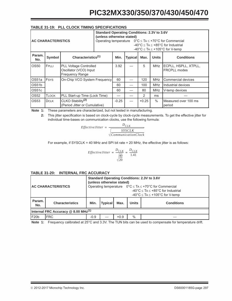
TABLE 31-20: INTERNAL FRC ACCURACY
AC CHARACTERISTICS
Standard Operating Conditions: 2.3V to 3.6V(unless otherwise stated)Operating temperature 0°C TA +70°C for Commercial
-40°C TA +85°C for Industrial -40°C TA +105°C for V-temp
Param. No. Characteristics Min. Typical Max. Units Conditions
Internal FRC Accuracy @ 8.00 MHz(1)
F20b FRC -0.9 — +0.9 % —Note 1: Frequency calibrated at 25°C and 3.3V. The TUN bits can be used to compensate for temperature drift.
2012-2017 Microchip Technology Inc. DS60001185G-page 297
PIC32MX330/350/370/430/450/470
TABLE 31-19: PLL CLOCK TIMING SPECIFICATIONS
AC CHARACTERISTICS
Standard Operating Conditions: 2.3V to 3.6V(unless otherwise stated)Operating temperature 0°C TA +70°C for Commercial
-40°C TA +85°C for Industrial -40°C TA +105°C for V-temp
Param.No. Symbol Characteristics(1) Min. Typical Max. Units Conditions
OS50 FPLLI PLL Voltage Controlled Oscillator (VCO) Input Frequency Range
3.92 — 5 MHz ECPLL, HSPLL, XTPLL, FRCPLL modes
OS51a FSYS On-Chip VCO System Frequency 60 — 120 MHz Commercial devicesOS51b 60 — 100 MHz Industrial devicesOS51c 60 — 80 MHz V-temp devicesOS52 TLOCK PLL Start-up Time (Lock Time) — — 2 ms —OS53 DCLK CLKO Stability(2)
(Period Jitter or Cumulative)-0.25 — +0.25 % Measured over 100 ms
periodNote 1: These parameters are characterized, but not tested in manufacturing.
2: This jitter specification is based on clock-cycle by clock-cycle measurements. To get the effective jitter for individual time-bases on communication clocks, use the following formula:
For example, if SYSCLK = 40 MHz and SPI bit rate = 20 MHz, the effective jitter is as follows:
EffectiveJitterDCLK
SYSCLKCommunicationClock----------------------------------------------------------
---------------------------------------------------------------=
EffectiveJitterDCLK
4020------
--------------DCLK
1.41--------------= =

TABLE 31-21: INTERNAL LPRC ACCURACY
AC CHARACTERISTICS
Standard Operating Conditions: 2.3V to 3.6V(unless otherwise stated)Operating temperature 0°C TA +70°C for Commercial
-40°C TA +85°C for Industrial -40°C TA +105°C for V-temp
Param.No. Characteristics Min. Typical Max. Units Conditions
LPRC @ 31.25 kHz(1)
F21 LPRC -15 — +15 % —Note 1: Change of LPRC frequency as VDD changes.
PIC32MX330/350/370/430/450/470
DS60001185G-page 298 2012-2017 Microchip Technology Inc.
FIGURE 31-3: I/O TIMING CHARACTERISTICS
Note: Refer to Figure 31-1 for load conditions.
I/O Pin(Input)
I/O Pin(Output)
DI35DI40
DO31DO32
TABLE 31-22: I/O TIMING REQUIREMENTS
AC CHARACTERISTICS
Standard Operating Conditions: 2.3V to 3.6V(unless otherwise stated)Operating temperature 0°C TA +70°C for Commercial
-40°C TA +85°C for Industrial -40°C TA +105°C for V-temp
Param.No. Symbol Characteristics(2) Min. Typical(1) Max. Units Conditions
TIOR Port Output Rise Time — 5 15 ns VDD < 2.5V
— 5 10 ns VDD > 2.5VTIOF Port Output Fall Time — 5 15 ns VDD < 2.5V
— 5 10 ns VDD > 2.5VDI35 TINP INTx Pin High or Low Time 10 — — ns —DI40 TRBP CNx High or Low Time (input) 2 — — TSYSCLK —Note 1: Data in “Typical” column is at 3.3V, 25°C unless otherwise stated.
2: This parameter is characterized, but not tested in manufacturing.
DO31
DO32

2012-2017 Microchip Technology Inc. DS60001185G-page 299
PIC32MX330/350/370/430/450/470FIGURE 31-4:
VDD
VPOR
Note 1: The power-up period will be extended if the power-up sequence completes before the device exits from BOR (VDD < VDDMIN).
2: Includes interval voltage regulator stabilization delay.
SY00
Power-up Sequence(Note 2)
Internal Voltage Regulator Enabled
(TPU)SY10
CPU Starts Fetching Code
Clock Sources = (HS, HSPLL, XT, XTPLL and SOSC)
VDD
VPOR
SY00
Power-up Sequence(Note 2)
Internal Voltage Regulator Enabled
(TPU)
(TSYSDLY)
CPU Starts Fetching Code
(Note 1)
(Note 1)
Clock Sources = (FRC, FRCDIV, FRCDIV16, FRCPLL, EC, ECPLL and LPRC)
(TOST)
SY02
(TSYSDLY)SY02
POWER-ON RESET TIMING CHARACTERISTICS

PIC32MX330/350/370/430/450/470
DS60001185G-page 300 2012-2017 Microchip Technology Inc.
FIGURE 31-5: EXTERNAL RESET TIMING CHARACTERISTICS
MCLR
(SY20)
Reset Sequence
(SY10)
CPU Starts Fetching Code
BOR
(SY30)
TOST
TMCLR
TBOR
Reset Sequence
CPU Starts Fetching Code
Clock Sources = (FRC, FRCDIV, FRCDIV16, FRCPLL, EC, ECPLL and LPRC)
Clock Sources = (HS, HSPLL, XT, XTPLL and SOSC) (TSYSDLY)SY02
(TSYSDLY)SY02
TABLE 31-23: RESETS TIMING
AC CHARACTERISTICS
Standard Operating Conditions: 2.3V to 3.6V(unless otherwise stated)Operating temperature 0°C TA +70°C for Commercial
Param.No. Symbol Characteristics(1) Min. Typical(2) Max. Units Conditions
SY00 TPU Power-up PeriodInternal Voltage Regulator Enabled
— 400 600 s —
SY02 TSYSDLY System Delay Period: Time Required to Reload Device Configuration Fuses plus SYSCLK Delay before First instruction is Fetched.
— s + 8 SYSCLK
cycles
— — —
SY20 TMCLR MCLR Pulse Width (low) 2 — — s —
SY30 TBOR BOR Pulse Width (low) — 1 — s —Note 1: These parameters are characterized, but not tested in manufacturing.
2: Data in “Typ” column is at 3.3V, 25°C unless otherwise stated. Characterized by design but not tested.
-40°C TA +85°C for Industrial -40°C TA +105°C for V-temp

2012-2017 Microchip Technology Inc. DS60001185G-page 301
PIC32MX330/350/370/430/450/470FIGURE 31-6: TIMER1, 2, 3, 4, 5 EXTERNAL CLOCK TIMING CHARACTERISTICS
Note: Refer to Figure 31-1 for load conditions.
Tx11
Tx15
Tx10
Tx20
TMRx
OS60
TxCK
TABLE 31-24: TIMER1 EXTERNAL CLOCK TIMING REQUIREMENTS(1)
AC CHARACTERISTICS
Standard Operating Conditions: 2.3V to 3.6V(unless otherwise stated)Operating temperature 0°C TA +70°C for Commercial
-40°C TA +85°C for Industrial -40°C TA +105°C for V-temp
Param.No. Symbol Characteristics(2) Min. Typical Max. Units Conditions
TA10 TTXH TxCK High Time
Synchronous, with prescaler
[(12.5 ns or 1 TPB)/N] + 25 ns
— — ns Must also meet parameter TA15
Asynchronous, with prescaler
10 — — ns —
TA11 TTXL TxCK Low Time
Synchronous, with prescaler
[(12.5 ns or 1 TPB)/N] + 25 ns
— — ns Must also meet parameter TA15
Asynchronous, with prescaler
10 — — ns —
TA15 TTXP TxCK Input Period
Synchronous, with prescaler
[(Greater of 25 ns or 2 TPB)/N] + 30 ns
— — ns VDD > 2.7V
[(Greater of 25 ns or 2 TPB)/N] + 50 ns
— — ns VDD < 2.7V
Asynchronous, with prescaler
20 — — ns VDD > 2.7V (Note 3)
50 — — ns VDD < 2.7V (Note 3)
OS60 FT1 SOSC1/T1CK Oscillator Input Frequency Range (oscillator enabled by setting TCS bit (T1CON<1>))
32 — 100 kHz —
TA20 TCKEXTMRL Delay from External TxCK Clock Edge to Timer Increment
— 1 TPB —
Note 1: Timer1 is a Type A.2: This parameter is characterized, but not tested in manufacturing.3: N = Prescale Value (1, 8, 64, 256).

PIC32MX330/350/370/430/450/470
DS60001185G-page 302 2012-2017 Microchip Technology Inc.
FIGURE 31-7: INPUT CAPTURE (CAPx) TIMING CHARACTERISTICS
ICx
IC10 IC11
IC15
Note: Refer to Figure 31-1 for load conditions.
TABLE 31-26: INPUT CAPTURE MODULE TIMING REQUIREMENTS
AC CHARACTERISTICS
Standard Operating Conditions: 2.3V to 3.6V(unless otherwise stated)Operating temperature 0°C TA +70°C for Commercial
-40°C TA +85°C for Industrial -40°C TA +105°C for V-temp
Param.No. Symbol Characteristics(1) Min. Max. Units Conditions
IC10 TCCL ICx Input Low Time [(12.5 ns or 1 TPB)/N] + 25 ns
— ns Must also meet parameter IC15.
N = prescale value (1, 4, 16)
IC11 TCCH ICx Input High Time [(12.5 ns or 1 TPB)/N] + 25 ns
— ns Must also meet parameter IC15.
IC15 TCCP ICx Input Period [(25 ns or 2 TPB)/N] + 50 ns
— ns —
Note 1: These parameters are characterized, but not tested in manufacturing.
TABLE 31-25: TIMER2, 3, 4, 5 EXTERNAL CLOCK TIMING REQUIREMENTS
AC CHARACTERISTICS
Standard Operating Conditions: 2.3V to 3.6V(unless otherwise stated)Operating temperature 0°C TA +70°C for Commercial
-40°C TA +85°C for Industrial -40°C TA +105°C for V-temp
Param.No. Symbol Characteristics(1) Min. Max. Units Conditions
TB10 TTXH TxCKHigh Time
Synchronous, with prescaler
[(12.5 ns or 1 TPB)/N] + 25 ns
— ns Must also meet parameter TB15
N = prescale value (1, 2, 4, 8, 16, 32, 64, 256)
TB11 TTXL TxCKLow Time
Synchronous, with prescaler
[(12.5 ns or 1 TPB)/N] + 25 ns
— ns Must also meet parameter TB15
TB15 TTXP TxCK Input Period
Synchronous, with prescaler
[(Greater of [(25 ns or 2 TPB)/N] + 30 ns
— ns VDD > 2.7V
[(Greater of [(25 ns or 2 TPB)/N] + 50 ns
— ns VDD < 2.7V
TB20 TCKEXTMRL Delay from External TxCK Clock Edge to Timer Increment
— 1 TPB —
Note 1: These parameters are characterized, but not tested in manufacturing.

2012-2017 Microchip Technology Inc. DS60001185G-page 303
PIC32MX330/350/370/430/450/470FIGURE 31-8: OUTPUT COMPARE MODULE (OCx) TIMING CHARACTERISTICS
OCx
OC11 OC10(Output Compare
Note: Refer to Figure 31-1 for load conditions.
or PWM mode)
TABLE 31-27: OUTPUT COMPARE MODULE TIMING REQUIREMENTS
AC CHARACTERISTICS
Standard Operating Conditions: 2.3V to 3.6V(unless otherwise stated)Operating temperature 0°C TA +70°C for Commercial
-40°C TA +85°C for Industrial -40°C TA +105°C for V-temp
Param. No. Symbol Characteristics(1) Min. Typical(2) Max. Units Conditions
OC10 TCCF OCx Output Fall Time — — — nsOC11 TCCR OCx Output Rise Time — — — nsNote 1: These parameters are characterized, but not tested in manufacturing.
2: Data in “Typical” column is at 3.3V, 25°C unless otherwise stated. Parameters are for design guidance only and are not tested.
FIGURE 31-9: OCx/PWM MODULE TIMING CHARACTERISTICS
OCFA/OCFB
OCx
OC20
OC15
Note: Refer to Figure 31-1 for load conditions.
OCx is tri-stated
TABLE 31-28: SIMPLE OCx/PWM MODE TIMING REQUIREMENTS
AC CHARACTERISTICS
Standard Operating Conditions: 2.3V to 3.6V(unless otherwise stated)Operating temperature 0°C TA +70°C for Commercial
-40°C TA +85°C for Industrial -40°C TA +105°C for V-temp
Param No. Symbol Characteristics(1) Min Typical(2) Max Units Conditions
OC15 TFD Fault Input to PWM I/O Change — — 50 ns —OC20 TFLT Fault Input Pulse Width 50 — — ns —Note 1: These parameters are characterized, but not tested in manufacturing.
2: Data in “Typical” column is at 3.3V, 25°C unless otherwise stated. Parameters are for design guidance only and are not tested.
See parameter DO32See parameter DO31

PIC32MX330/350/370/430/450/470
DS60001185G-page 304 2012-2017 Microchip Technology Inc.
FIGURE 31-10: SPIx MODULE MASTER MODE (CKE = 0) TIMING CHARACTERISTICS
SCKx(CKP = 0)
SCKx(CKP = 1)
SDOx
SDIx
SP11 SP10
SP40 SP41
SP21SP20SP35
SP20SP21
MSb LSbBit 14 - - - - - -1
MSb In LSb InBit 14 - - - -1
SP30SP31
Note: Refer to Figure 31-1 for load conditions.
TABLE 31-29: SPIx MASTER MODE (CKE = 0) TIMING REQUIREMENTS
AC CHARACTERISTICS
Standard Operating Conditions: 2.3V to 3.6V(unless otherwise stated)Operating temperature 0°C TA +70°C for Commercial
-40°C TA +85°C for Industrial -40°C TA +105°C for V-temp
Param.No. Symbol Characteristics(1) Min. Typical(2) Max. Units Conditions
SP10 TSCL SCKx Output Low Time (Note 3)
TSCK/2 — — ns —
SP11 TSCH SCKx Output High Time (Note 3)
TSCK/2 — — ns —
SP20 TSCF SCKx Output Fall Time (Note 4)
— — — ns See parameter DO32
SP21 TSCR SCKx Output Rise Time (Note 4)
— — — ns See parameter DO31
SP30 TDOF SDOx Data Output Fall Time (Note 4)
— — — ns See parameter DO32
SP31 TDOR SDOx Data Output Rise Time (Note 4)
— — — ns See parameter DO31
SP35 TSCH2DOV, TSCL2DOV
SDOx Data Output Valid after SCKx Edge
— — 15 ns VDD > 2.7V
— — 20 ns VDD < 2.7V
SP40 TDIV2SCH, TDIV2SCL
Setup Time of SDIx Data Input to SCKx Edge
10 — — ns —
SP41 TSCH2DIL, TSCL2DIL
Hold Time of SDIx Data Input to SCKx Edge
10 — — ns —
Note 1: These parameters are characterized, but not tested in manufacturing.2: Data in “Typical” column is at 3.3V, 25°C unless otherwise stated. Parameters are for design guidance
only and are not tested.3: The minimum clock period for SCKx is 40 ns. Therefore, the clock generated in Master mode must not
violate this specification.4: Assumes 50 pF load on all SPIx pins.

2012-2017 Microchip Technology Inc. DS60001185G-page 305
PIC32MX330/350/370/430/450/470FIGURE 31-11: SPIx MODULE MASTER MODE (CKE = 1) TIMING CHARACTERISTICS
SCKX(CKP = 0)
SCKX(CKP = 1)
SDOX
SDIX
SP36
SP30,SP31
SP35
MSb Bit 14 - - - - - -1
LSb InBit 14 - - - -1
LSb
Note: Refer to Figure 31-1 for load conditions.
SP11 SP10
SP21SP20
SP40 SP41
SP20SP21
MSb In
TABLE 31-30: SPIx MODULE MASTER MODE (CKE = 1) TIMING REQUIREMENTS
AC CHARACTERISTICS
Standard Operating Conditions: 2.3V to 3.6V(unless otherwise stated)Operating temperature 0°C TA +70°C for Commercial
-40°C TA +85°C for Industrial -40°C TA +105°C for V-temp
Param.No. Symbol Characteristics(1) Min. Typ.(2) Max. Units Conditions
SP10 TSCL SCKx Output Low Time (Note 3) TSCK/2 — — ns —SP11 TSCH SCKx Output High Time (Note 3) TSCK/2 — — ns —SP20 TSCF SCKx Output Fall Time (Note 4) — — — ns See parameter DO32SP21 TSCR SCKx Output Rise Time (Note 4) — — — ns See parameter DO32SP30 TDOF SDOx Data Output Fall Time
(Note 4)— — — ns See parameter DO32
SP31 TDOR SDOx Data Output Rise Time (Note 4)
— — — ns See parameter DO31
SP35 TSCH2DOV,TSCL2DOV
SDOx Data Output Valid after SCKx Edge
— — 15 ns VDD > 2.7V— — 20 ns VDD < 2.7V
SP36 TDOV2SC, TDOV2SCL
SDOx Data Output Setup to First SCKx Edge
15 — — ns —
SP40 TDIV2SCH, TDIV2SCL
Setup Time of SDIx Data Input to SCKx Edge
15 — — ns VDD > 2.7V20 — — ns VDD < 2.7V
SP41 TSCH2DIL, TSCL2DIL
Hold Time of SDIx Data Input to SCKx Edge
15 — — ns VDD > 2.7V20 — — ns VDD < 2.7V
Note 1: These parameters are characterized, but not tested in manufacturing.2: Data in “Typical” column is at 3.3V, 25°C unless otherwise stated. Parameters are for design guidance only
and are not tested.3: The minimum clock period for SCKx is 40 ns. Therefore, the clock generated in Master mode must not
violate this specification.4: Assumes 50 pF load on all SPIx pins.

PIC32MX330/350/370/430/450/470
DS60001185G-page 306 2012-2017 Microchip Technology Inc.
FIGURE 31-12: SPIx MODULE SLAVE MODE (CKE = 0) TIMING CHARACTERISTICS
SSX
SCKX(CKP = 0)
SCKX(CKP = 1)
SDOX
SP50
SP40 SP41
SP30,SP31 SP51
SP35
MSb LSbBit 14 - - - - - -1
Bit 14 - - - -1 LSb In
SP52
SP73SP72
SP72SP73SP71 SP70
Note: Refer to Figure 31-1 for load conditions.
SDIX MSb In
TABLE 31-31: SPIx MODULE SLAVE MODE (CKE = 0) TIMING REQUIREMENTS
AC CHARACTERISTICS
Standard Operating Conditions: 2.3V to 3.6V(unless otherwise stated)Operating temperature 0°C TA +70°C for Commercial
-40°C TA +85°C for Industrial -40°C TA +105°C for V-temp
Param.No. Symbol Characteristics(1) Min. Typ.(2) Max. Units Conditions
SP70 TSCL SCKx Input Low Time (Note 3) TSCK/2 — — ns —SP71 TSCH SCKx Input High Time (Note 3) TSCK/2 — — ns —SP72 TSCF SCKx Input Fall Time — — — ns See parameter DO32SP73 TSCR SCKx Input Rise Time — — — ns See parameter DO31SP30 TDOF SDOx Data Output Fall Time
(Note 4)— — — ns See parameter DO32
SP31 TDOR SDOx Data Output Rise Time (Note 4)
— — — ns See parameter DO31
SP35 TSCH2DOV,TSCL2DOV
SDOx Data Output Valid after SCKx Edge
— — 15 ns VDD > 2.7V— — 20 ns VDD < 2.7V
SP40 TDIV2SCH, TDIV2SCL
Setup Time of SDIx Data Input to SCKx Edge
10 — — ns —
SP41 TSCH2DIL, TSCL2DIL
Hold Time of SDIx Data Input to SCKx Edge
10 — — ns —
SP50 TSSL2SCH, TSSL2SCL
SSx to SCKx or SCKx Input 175 — — ns —
SP51 TSSH2DOZ SSx to SDOx Output High-Impedance (Note 3)
5 — 25 ns —
Note 1: These parameters are characterized, but not tested in manufacturing.2: Data in “Typical” column is at 3.3V, 25°C unless otherwise stated. Parameters are for design guidance only
and are not tested.3: The minimum clock period for SCKx is 40 ns.4: Assumes 50 pF load on all SPIx pins.

2012-2017 Microchip Technology Inc. DS60001185G-page 307
PIC32MX330/350/370/430/450/470
SP52 TSCH2SSHTSCL2SSH
SSx after SCKx Edge TSCK + 20
— — ns —
TABLE 31-31: SPIx MODULE SLAVE MODE (CKE = 0) TIMING REQUIREMENTS (CONTINUED)
AC CHARACTERISTICS
Standard Operating Conditions: 2.3V to 3.6V(unless otherwise stated)Operating temperature 0°C TA +70°C for Commercial
-40°C TA +85°C for Industrial -40°C TA +105°C for V-temp
Param.No. Symbol Characteristics(1) Min. Typ.(2) Max. Units Conditions
Note 1: These parameters are characterized, but not tested in manufacturing.2: Data in “Typical” column is at 3.3V, 25°C unless otherwise stated. Parameters are for design guidance only
and are not tested.3: The minimum clock period for SCKx is 40 ns.4: Assumes 50 pF load on all SPIx pins.

PIC32MX330/350/370/430/450/470
DS60001185G-page 308 2012-2017 Microchip Technology Inc.
FIGURE 31-13: SPIx MODULE SLAVE MODE (CKE = 1) TIMING CHARACTERISTICS
SSx
SCKx(CKP = 0)
SCKx(CKP = 1)
SDOx
SDI
SP60
SDIx
SP30,SP31
MSb Bit 14 - - - - - -1 LSb
SP51
MSb In Bit 14 - - - -1 LSb In
SP52
SP73SP72
SP72SP73SP71
SP40 SP41
Note: Refer to Figure 31-1 for load conditions.
SP50
SP70
SP35
TABLE 31-32: SPIx MODULE SLAVE MODE (CKE = 1) TIMING REQUIREMENTS
AC CHARACTERISTICS
Standard Operating Conditions: 2.3V to 3.6V(unless otherwise stated)Operating temperature 0°C TA +70°C for Commercial
-40°C TA +85°C for Industrial -40°C TA +105°C for V-temp
Param.No. Symbol Characteristics(1) Min. Typical(2) Max. Units Conditions
SP70 TSCL SCKx Input Low Time (Note 3) TSCK/2 — — ns —SP71 TSCH SCKx Input High Time (Note 3) TSCK/2 — — ns —SP72 TSCF SCKx Input Fall Time — 5 10 ns —SP73 TSCR SCKx Input Rise Time — 5 10 ns —SP30 TDOF SDOx Data Output Fall Time
(Note 4)— — — ns See parameter DO32
SP31 TDOR SDOx Data Output Rise Time (Note 4)
— — — ns See parameter DO31
SP35 TSCH2DOV,TSCL2DOV
SDOx Data Output Valid after SCKx Edge
— — 20 ns VDD > 2.7V— — 30 ns VDD < 2.7V
SP40 TDIV2SCH, TDIV2SCL
Setup Time of SDIx Data Input to SCKx Edge
10 — — ns —
SP41 TSCH2DIL, TSCL2DIL
Hold Time of SDIx Data Input to SCKx Edge
10 — — ns —
Note 1: These parameters are characterized, but not tested in manufacturing.2: Data in “Typical” column is at 3.3V, 25°C unless otherwise stated. Parameters are for design guidance only
and are not tested.3: The minimum clock period for SCKx is 40 ns. 4: Assumes 50 pF load on all SPIx pins.

2012-2017 Microchip Technology Inc. DS60001185G-page 309
PIC32MX330/350/370/430/450/470
SP50 TSSL2SCH, TSSL2SCL
SSx to SCKx or SCKx Input 175 — — ns —
SP51 TSSH2DOZ SSx to SDOX Output High-Impedance (Note 4)
5 — 25 ns —
SP52 TSCH2SSHTSCL2SSH
SSx after SCKx Edge TSCK + 20
— — ns —
SP60 TSSL2DOV SDOx Data Output Valid after SSx Edge
— — 25 ns —
TABLE 31-32: SPIx MODULE SLAVE MODE (CKE = 1) TIMING REQUIREMENTS (CONTINUED)
AC CHARACTERISTICS
Standard Operating Conditions: 2.3V to 3.6V(unless otherwise stated)Operating temperature 0°C TA +70°C for Commercial
-40°C TA +85°C for Industrial -40°C TA +105°C for V-temp
Param.No. Symbol Characteristics(1) Min. Typical(2) Max. Units Conditions
Note 1: These parameters are characterized, but not tested in manufacturing.2: Data in “Typical” column is at 3.3V, 25°C unless otherwise stated. Parameters are for design guidance only
and are not tested.3: The minimum clock period for SCKx is 40 ns. 4: Assumes 50 pF load on all SPIx pins.

PIC32MX330/350/370/430/450/470
DS60001185G-page 310 2012-2017 Microchip Technology Inc.
FIGURE 31-14: I2Cx BUS START/STOP BITS TIMING CHARACTERISTICS (MASTER MODE)
SCLx
SDAx
StartCondition
StopCondition
Note: Refer to Figure 31-1 for load conditions.
IM30
IM31 IM34
IM33
FIGURE 31-15: I2Cx BUS DATA TIMING CHARACTERISTICS (MASTER MODE)
IM11IM10 IM33
IM11IM10
IM20
IM26IM25
IM40 IM40 IM45
IM21
SCLx
SDAxIn
SDAxOut
Note: Refer to Figure 31-1 for load conditions.

2012-2017 Microchip Technology Inc. DS60001185G-page 311
PIC32MX330/350/370/430/450/470
TABLE 31-33: I2Cx BUS DATA TIMING REQUIREMENTS (MASTER MODE)
AC CHARACTERISTICS
Standard Operating Conditions: 2.3V to 3.6V(unless otherwise stated)Operating temperature 0°C TA +70°C for Commercial
-40°C TA +85°C for Industrial -40°C TA +105°C for V-temp
Param.No. Symbol Characteristics Min.(1) Max. Units Conditions
IM10 TLO:SCL Clock Low Time 100 kHz mode TPB * (BRG + 2) — s —400 kHz mode TPB * (BRG + 2) — s —1 MHz mode (Note 2)
TPB * (BRG + 2) — s —
IM11 THI:SCL Clock High Time 100 kHz mode TPB * (BRG + 2) — s —400 kHz mode TPB * (BRG + 2) — s —1 MHz mode (Note 2)
TPB * (BRG + 2) — s —
IM20 TF:SCL SDAx and SCLx Fall Time
100 kHz mode — 300 ns CB is specified to be from 10 to 400 pF400 kHz mode 20 + 0.1 CB 300 ns
1 MHz mode (Note 2)
— 100 ns
IM21 TR:SCL SDAx and SCLx Rise Time
100 kHz mode — 1000 ns CB is specified to be from 10 to 400 pF400 kHz mode 20 + 0.1 CB 300 ns
1 MHz mode (Note 2)
— 300 ns
IM25 TSU:DAT Data Input Setup Time
100 kHz mode 250 — ns —400 kHz mode 100 — ns1 MHz mode (Note 2)
100 — ns
IM26 THD:DAT Data Input Hold Time
100 kHz mode 0 — s —400 kHz mode 0 0.9 s1 MHz mode (Note 2)
0 0.3 s
IM30 TSU:STA Start Condition Setup Time
100 kHz mode TPB * (BRG + 2) — s Only relevant for Repeated Start condition
400 kHz mode TPB * (BRG + 2) — s1 MHz mode (Note 2)
TPB * (BRG + 2) — s
IM31 THD:STA Start Condition Hold Time
100 kHz mode TPB * (BRG + 2) — s After this period, the first clock pulse is generated
400 kHz mode TPB * (BRG + 2) — s1 MHz mode (Note 2)
TPB * (BRG + 2) — s
IM33 TSU:STO Stop Condition Setup Time
100 kHz mode TPB * (BRG + 2) — s —400 kHz mode TPB * (BRG + 2) — s1 MHz mode (Note 2)
TPB * (BRG + 2) — s
Note 1: BRG is the value of the I2C Baud Rate Generator. 2: Maximum pin capacitance = 10 pF for all I2Cx pins (for 1 MHz mode only).3: The typical value for this parameter is 104 ns.

PIC32MX330/350/370/430/450/470
DS60001185G-page 312 2012-2017 Microchip Technology Inc.
IM34 THD:STO Stop Condition 100 kHz mode TPB * (BRG + 2) — ns —Hold Time 400 kHz mode TPB * (BRG + 2) — ns
1 MHz mode (Note 2)
TPB * (BRG + 2) — ns
IM40 TAA:SCL Output Valid from Clock
100 kHz mode — 3500 ns —400 kHz mode — 1000 ns —1 MHz mode (Note 2)
— 350 ns —
IM45 TBF:SDA Bus Free Time 100 kHz mode 4.7 — s The amount of time the bus must be free before a new transmission can start
400 kHz mode 1.3 — s1 MHz mode (Note 2)
0.5 — s
IM50 CB Bus Capacitive Loading — 400 pF —IM51 TPGD Pulse Gobbler Delay 52 312 ns See Note 3
TABLE 31-33: I2Cx BUS DATA TIMING REQUIREMENTS (MASTER MODE) (CONTINUED)
AC CHARACTERISTICS
Standard Operating Conditions: 2.3V to 3.6V(unless otherwise stated)Operating temperature 0°C TA +70°C for Commercial
-40°C TA +85°C for Industrial -40°C TA +105°C for V-temp
Param.No. Symbol Characteristics Min.(1) Max. Units Conditions
Note 1: BRG is the value of the I2C Baud Rate Generator. 2: Maximum pin capacitance = 10 pF for all I2Cx pins (for 1 MHz mode only).3: The typical value for this parameter is 104 ns.

2012-2017 Microchip Technology Inc. DS60001185G-page 313
PIC32MX330/350/370/430/450/470FIGURE 31-16: I2Cx BUS START/STOP BITS TIMING CHARACTERISTICS (SLAVE MODE)
IS34SCLx
SDAx
StartCondition
StopCondition
IS33
Note: Refer to Figure 31-1 for load conditions.
IS31
IS30
FIGURE 31-17: I2Cx BUS DATA TIMING CHARACTERISTICS (SLAVE MODE)
IS30IS31 IS33
IS11
IS10
IS20
IS26IS25
IS40 IS40 IS45
IS21
SCLx
SDAxIn
SDAxOut
Note: Refer to Figure 31-1 for load conditions.

PIC32MX330/350/370/430/450/470
DS60001185G-page 314 2012-2017 Microchip Technology Inc.
TABLE 31-34: I2Cx BUS DATA TIMING REQUIREMENTS (SLAVE MODE)
AC CHARACTERISTICS
Standard Operating Conditions: 2.3V to 3.6V(unless otherwise stated)Operating temperature 0°C TA +70°C for Commercial
-40°C TA +85°C for Industrial -40°C TA +105°C for V-temp
Param. No. Symbol Characteristics Min. Max. Units Conditions
IS10 TLO:SCL Clock Low Time 100 kHz mode 4.7 — s PBCLK must operate at a minimum of 800 kHz
400 kHz mode 1.3 — s PBCLK must operate at a minimum of 3.2 MHz
1 MHz mode (Note 1)
0.5 — s —
IS11 THI:SCL Clock High Time 100 kHz mode 4.0 — s PBCLK must operate at a minimum of 800 kHz
400 kHz mode 0.6 — s PBCLK must operate at a minimum of 3.2 MHz
1 MHz mode (Note 1)
0.5 — s —
IS20 TF:SCL SDAx and SCLx Fall Time
100 kHz mode — 300 ns CB is specified to be from 10 to 400 pF400 kHz mode 20 + 0.1 CB 300 ns
1 MHz mode (Note 1)
— 100 ns
IS21 TR:SCL SDAx and SCLx Rise Time
100 kHz mode — 1000 ns CB is specified to be from 10 to 400 pF400 kHz mode 20 + 0.1 CB 300 ns
1 MHz mode (Note 1)
— 300 ns
IS25 TSU:DAT Data Input Setup Time
100 kHz mode 250 — ns —400 kHz mode 100 — ns1 MHz mode (Note 1)
100 — ns
IS26 THD:DAT Data Input Hold Time
100 kHz mode 0 — ns —400 kHz mode 0 0.9 s1 MHz mode (Note 1)
0 0.3 s
IS30 TSU:STA Start Condition Setup Time
100 kHz mode 4700 — ns Only relevant for Repeated Start condition400 kHz mode 600 — ns
1 MHz mode (Note 1)
250 — ns
IS31 THD:STA Start Condition Hold Time
100 kHz mode 4000 — ns After this period, the first clock pulse is generated400 kHz mode 600 — ns
1 MHz mode (Note 1)
250 — ns
IS33 TSU:STO Stop Condition Setup Time
100 kHz mode 4000 — ns —400 kHz mode 600 — ns1 MHz mode (Note 1)
600 — ns
Note 1: Maximum pin capacitance = 10 pF for all I2Cx pins (for 1 MHz mode only).

2012-2017 Microchip Technology Inc. DS60001185G-page 315
PIC32MX330/350/370/430/450/470
IS34 THD:STO Stop ConditionHold Time
100 kHz mode 4000 — ns —400 kHz mode 600 — ns1 MHz mode (Note 1)
250 ns
IS40 TAA:SCL Output Valid from Clock
100 kHz mode 0 3500 ns —400 kHz mode 0 1000 ns1 MHz mode (Note 1)
0 350 ns
IS45 TBF:SDA Bus Free Time 100 kHz mode 4.7 — s The amount of time the bus must be free before a new transmission can start
400 kHz mode 1.3 — s1 MHz mode (Note 1)
0.5 — s
IS50 CB Bus Capacitive Loading — 400 pF —
TABLE 31-34: I2Cx BUS DATA TIMING REQUIREMENTS (SLAVE MODE) (CONTINUED)
AC CHARACTERISTICS
Standard Operating Conditions: 2.3V to 3.6V(unless otherwise stated)Operating temperature 0°C TA +70°C for Commercial
-40°C TA +85°C for Industrial -40°C TA +105°C for V-temp
Param. No. Symbol Characteristics Min. Max. Units Conditions
Note 1: Maximum pin capacitance = 10 pF for all I2Cx pins (for 1 MHz mode only).

PIC32MX330/350/370/430/450/470
DS60001185G-page 316 2012-2017 Microchip Technology Inc.
TABLE 31-35: ADC MODULE SPECIFICATIONS
AC CHARACTERISTICS(5)
Standard Operating Conditions: 2.3V to 3.6V(unless otherwise stated)Operating temperature 0°C TA +70°C for Commercial
-40°C TA +85°C for Industrial -40°C TA +105°C for V-temp
Param. No. Symbol Characteristics Min. Typical Max. Units Conditions
Device SupplyAD01 AVDD Module VDD Supply Greater of
VDD – 0.3or 2.5
— Lesser ofVDD + 0.3
or 3.6
V—
AD02 AVSS Module VSS Supply VSS — VSS + 0.3 V —Reference Inputs AD05 VREFH Reference Voltage High AVSS + 2.0 — AVDD V (Note 1)AD05a 2.5 — 3.6 V VREFH = AVDD (Note 3)AD06 VREFL Reference Voltage Low AVSS — VREFH – 2.0 V (Note 1)AD07 VREF Absolute Reference
Voltage (VREFH – VREFL)2.0 — AVDD V (Note 3)
AD08 IREF Current Drain — 250—
4003
AA
ADC operating ADC off
Analog InputAD12 VINH-VINL Full-Scale Input Span VREFL — VREFH V —AD13 VINL Absolute VINL Input
VoltageAVSS – 0.3 — AVDD/2 V —
AD14 VIN Absolute Input Voltage AVSS – 0.3 — AVDD + 0.3 V —AD15 Leakage Current — +/- 0.001 +/-0.610 A VINL = AVSS = VREFL = 0V,
AVDD = VREFH = 3.3VSource Impedance = 10 k
AD17 RIN Recommended Impedance of Analog Voltage Source
— — 5K (Note 1)
ADC Accuracy – Measurements with External VREF+/VREF-AD20c Nr Resolution 10 data bits bits —AD21c INL Integral Nonlinearity > -1 — < 1 LSb VINL = AVSS = VREFL = 0V,
AVDD = VREFH = 3.3VAD22c DNL Differential Nonlinearity > -1 — < 1 LSb VINL = AVSS = VREFL = 0V,
AVDD = VREFH = 3.3V (Note 2)
AD23c GERR Gain Error > -1 — < 1 LSb VINL = AVSS = VREFL = 0V, AVDD = VREFH = 3.3V
AD24n EOFF Offset Error > -1 — < 1 LSb VINL = AVSS = 0V, AVDD = 3.3V
AD25c — Monotonicity — — — — GuaranteedNote 1: These parameters are not characterized or tested in manufacturing.
2: With no missing codes.3: These parameters are characterized, but not tested in manufacturing.4: Characterized with a 1 kHz sine wave.5: Overall functional device operation at VBORMIN < VDD < VDDMIN is tested, but not characterized. All device
Analog modules, such as ADC, etc., will function, but with degraded performance below VDDMIN. Refer to parameter BO10 in Table 31-10 for VBORMIN values.

2012-2017 Microchip Technology Inc. DS60001185G-page 317
PIC32MX330/350/370/430/450/470
ADC Accuracy – Measurements with Internal VREF+/VREF-AD20d Nr Resolution 10 data bits bits (Note 3)AD21d INL Integral Nonlinearity > -1 — < 1 LSb VINL = AVSS = 0V,
AVDD = 2.5V to 3.6V (Note 3)
AD22d DNL Differential Nonlinearity > -1 — < 1 LSb VINL = AVSS = 0V, AVDD = 2.5V to 3.6V (Notes 2,3)
AD23d GERR Gain Error > -4 — < 4 LSb VINL = AVSS = 0V, AVDD = 2.5V to 3.6V (Note 3)
AD24d EOFF Offset Error > -2 — < 2 LSb VINL = AVSS = 0V, AVDD = 2.5V to 3.6V (Note 3)
AD25d — Monotonicity — — — — GuaranteedDynamic PerformanceAD31b SINAD Signal to Noise and
Distortion55 58 — dB (Notes 3,4)
AD34b ENOB Effective Number of Bits 9 9.5 — bits (Notes 3,4)
TABLE 31-35: ADC MODULE SPECIFICATIONS (CONTINUED)
AC CHARACTERISTICS(5)
Standard Operating Conditions: 2.3V to 3.6V(unless otherwise stated)Operating temperature 0°C TA +70°C for Commercial
-40°C TA +85°C for Industrial -40°C TA +105°C for V-temp
Param. No. Symbol Characteristics Min. Typical Max. Units Conditions
Note 1: These parameters are not characterized or tested in manufacturing.2: With no missing codes.3: These parameters are characterized, but not tested in manufacturing.4: Characterized with a 1 kHz sine wave.5: Overall functional device operation at VBORMIN < VDD < VDDMIN is tested, but not characterized. All device
Analog modules, such as ADC, etc., will function, but with degraded performance below VDDMIN. Refer to parameter BO10 in Table 31-10 for VBORMIN values.

PIC32MX330/350/370/430/450/470
DS60001185G-page 318 2012-2017 Microchip Technology Inc.
TABLE 31-36: 10-BIT CONVERSION RATE PARAMETERS
AC CHARACTERISTICS(2)
Standard Operating Conditions: 2.3V to 3.6V(unless otherwise stated)Operating temperature 0°C TA +70°C for Commercial
-40°C TA +85°C for Industrial -40°C TA +105°C for V-temp
ADC Input ADC Speed TAD Min.
Sampling Time Min.
RS Max. VDD ADC Channels Configuration
AN0-AN14 1 Msps to 400 ksps(1)
65 ns 132 ns 500 3.0V to 3.6V
Up to 400 ksps 200 ns 200 ns 5.0 k 2.5V to 3.6V
AN15-AN27 400 ksps(1) 154 ns 1000 ns 500 3.0V to 3.6V
Note 1: External VREF- and VREF+ pins must be used for correct operation.2: These parameters are characterized, but not tested in manufacturing.
VREF- VREF+
ADCANx
SHACHX
VREF- VREF+
ADCANx
SHACHX
ANx or VREF-
orAVSS
orAVDD
VREF- VREF+
ADCANx
SHACHX

2012-2017 Microchip Technology Inc. DS60001185G-page 319
PIC32MX330/350/370/430/450/470
TABLE 31-37: ANALOG-TO-DIGITAL CONVERSION TIMING REQUIREMENTS
AC CHARACTERISTICS
Standard Operating Conditions: 2.3V to 3.6V(unless otherwise stated)Operating temperature 0°C TA +70°C for Commercial
-40°C TA +85°C for Industrial -40°C TA +105°C for V-temp
Param. No. Symbol Characteristics Min. Typical(1) Max. Units Conditions
Clock ParametersAD50 TAD ADC Clock Period(2) 65 — — ns See Table 31-36Conversion RateAD55 TCONV Conversion Time — 12 TAD — — —AD56 FCNV Throughput Rate
(Sampling Speed)(4)— — 1000 ksps AVDD = 3.0V to 3.6V— — 400 ksps AVDD = 2.5V to 3.6V
AD57 TSAMP Sample Time 2 TAD — — — —Timing ParametersAD60 TPCS Conversion Start from Sample
Trigger(3)— 1.0 TAD — — Auto-Convert Trigger
(SSRC<2:0> = 111) not selected
AD61 TPSS Sample Start from Setting Sample (SAMP) bit
0.5 TAD — 1.5 TAD — —
AD62 TCSS Conversion Completion to Sample Start (ASAM = 1)(3)
— 0.5 TAD — — —
AD63 TDPU Time to Stabilize Analog Stage from ADC Off to ADC On(3)
— — 2 s —
Note 1: These parameters are characterized, but not tested in manufacturing.2: Because the sample caps will eventually lose charge, clock rates below 10 kHz can affect linearity
performance, especially at elevated temperatures.3: Characterized by design but not tested.4: Refer to Table 31-36 for detailed conditions.
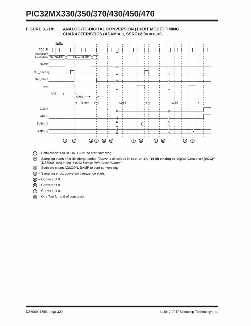
PIC32MX330/350/370/430/450/470
DS60001185G-page 320 2012-2017 Microchip Technology Inc.
FIGURE 31-18: ANALOG-TO-DIGITAL CONVERSION (10-BIT MODE) TIMING CHARACTERISTICS (ASAM = 0, SSRC<2:0> = 000)
AD55TSAMP
Clear SAMPSet SAMP
AD61
ADCLKInstruction
SAMP
ch0_dischrg
AD60
CONV
ADxIF
Buffer(0)
Buffer(1)
1 2 3 4 5 6 8 5 6 7
1 – Software sets ADxCON. SAMP to start sampling.
2 – Sampling starts after discharge period. TSAMP is described in Section 17. “10-bit Analog-to-Digital Converter (ADC)”
3 – Software clears ADxCON. SAMP to start conversion.
4 – Sampling ends, conversion sequence starts.
5 – Convert bit 9.
8 – One TAD for end of conversion.
AD50
ch0_samp
eoc
7
AD55
8
6 – Convert bit 8.
7 – Convert bit 0.
Execution
(DS60001104) in the “PIC32 Family Reference Manual”.
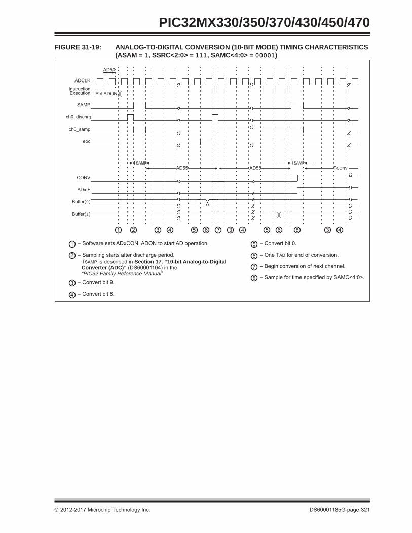
2012-2017 Microchip Technology Inc. DS60001185G-page 321
PIC32MX330/350/370/430/450/470FIGURE 31-19: ANALOG-TO-DIGITAL CONVERSION (10-BIT MODE) TIMING CHARACTERISTICS
(ASAM = 1, SSRC<2:0> = 111, SAMC<4:0> = 00001)
AD55TSAMP
Set ADON
ADCLK
Instruction
SAMP
ch0_dischrg
CONV
ADxIF
Buffer(0)
Buffer(1)
1 2 3 4 5 6 4 5 6 8
1 – Software sets ADxCON. ADON to start AD operation.
2 – Sampling starts after discharge period.
3 – Convert bit 9.
4 – Convert bit 8.
5 – Convert bit 0.
AD50
ch0_samp
eoc
7 3
AD55
6 – One TAD for end of conversion.
7 – Begin conversion of next channel.
8 – Sample for time specified by SAMC<4:0>.
TSAMPTCONV
3 4
Execution
TSAMP is described in Section 17. “10-bit Analog-to-Digital Converter (ADC)” (DS60001104) in the “PIC32 Family Reference Manual”

PIC32MX330/350/370/430/450/470
DS60001185G-page 322 2012-2017 Microchip Technology Inc.
FIGURE 31-20: PARALLEL SLAVE PORT TIMING
CS
RD
WR
PMD<7:0>
PS1
PS2
PS3
PS4
PS5
PS6
PS7
TABLE 31-38: PARALLEL SLAVE PORT REQUIREMENTS
AC CHARACTERISTICS
Standard Operating Conditions: 2.3V to 3.6V(unless otherwise stated)Operating temperature 0°C TA +70°C for Commercial
PS1 TdtV2wrH
Data In Valid before WR or CS Inactive (setup time)
20 — — ns —
PS2 TwrH2dtI
WR or CS Inactive to Data-In Invalid (hold time)
40 — — ns —
PS3 TrdL2dtV
RD and CS Active to Data-Out Valid
— — 60 ns —
PS4 TrdH2dtI RD Activeor CS Inactive to Data-Out Invalid
0 — 10 ns —
PS5 Tcs CS Active Time TPB + 40 — — ns —
PS6 TWR WR Active Time TPB + 25 — — ns —
PS7 TRD RD Active Time TPB + 25 — — ns —Note 1: These parameters are characterized, but not tested in manufacturing.
-40°C TA +85°C for Industrial -40°C TA +105°C for V-temp
Param.No. Symbol Characteristics(1) Min. Typ. Max. Units Conditions

2012-2017 Microchip Technology Inc. DS60001185G-page 323
PIC32MX330/350/370/430/450/470FIGURE 31-21: PARALLEL MASTER PORT READ TIMING DIAGRAM
TPB TPB TPB TPB TPB TPB TPB TPB
PB Clock
PMALL/PMALH
PMD<7:0>
PMA<x:8>
PMRD
PMCS<2:1>
PMWR
PM5
DataAddress<7:0>
PM1
PM3
PM6
Data
PM7
Address<7:0>
Address
PM4
PM2
TABLE 31-39: PARALLEL MASTER PORT READ TIMING REQUIREMENTS
AC CHARACTERISTICS
Standard Operating Conditions: 2.3V to 3.6V(unless otherwise stated)Operating temperature 0°C TA +70°C for Commercial
PM1 TLAT PMALL/PMALH Pulse Width — 1 TPB — — —PM2 TADSU Address Out Valid to PMALL/
PMALH Invalid (address setup time)
— 2 TPB — — —
PM3 TADHOLD PMALL/PMALH Invalid to Address Out Invalid (address hold time)
— 1 TPB — — —
PM4 TAHOLD PMRD Inactive to Address Out Invalid(address hold time)
5 — — ns —
PM5 TRD PMRD Pulse Width — 1 TPB — — —PM6 TDSU PMRD or PMENB Active to Data
In Valid (data setup time)15 — — ns —
PM7 TDHOLD PMRD or PMENB Inactive to Data In Invalid (data hold time)
1 TPB — — — PMP Clock
Note 1: These parameters are characterized, but not tested in manufacturing.
-40°C TA +85°C for Industrial -40°C TA +105°C for V-temp
Param. No. Symbol Characteristics(1) Min. Typ. Max. Units Conditions

PIC32MX330/350/370/430/450/470
DS60001185G-page 324 2012-2017 Microchip Technology Inc.
FIGURE 31-22: PARALLEL MASTER PORT WRITE TIMING DIAGRAM
TPB TPB TPB TPB TPB TPB TPB TPB
PB Clock
PMALL/PMALH
PMD<7:0>
PMA<x:8>
PMWR
PMCS<2:1>
PMRD
PM12PM13
PM11
Address
Address<7:0> Data
PM2 + PM3
PM1
TABLE 31-40: PARALLEL MASTER PORT WRITE TIMING REQUIREMENTS
AC CHARACTERISTICS
Standard Operating Conditions: 2.3V to 3.6V(unless otherwise stated)Operating temperature 0°C TA +70°C for Commercial
PM11 TWR PMWR Pulse Width — 1 TPB — — —PM12 TDVSU Data Out Valid before PMWR or
PMENB goes Inactive (data setup time)
— 2 TPB — — —
PM13 TDVHOLD PMWR or PMEMB Invalid to Data Out Invalid (data hold time)
— 1 TPB — — —
Note 1: These parameters are characterized, but not tested in manufacturing.
-40°C TA +85°C for Industrial -40°C TA +105°C for V-temp
Param. No. Symbol Characteristics(1) Min. Typ. Max. Units Conditions

2012-2017 Microchip Technology Inc. DS60001185G-page 325
PIC32MX330/350/370/430/450/470
TABLE 31-41: OTG ELECTRICAL SPECIFICATIONS
AC CHARACTERISTICS
Standard Operating Conditions: 2.3V to 3.6V(unless otherwise stated)Operating temperature 0°C TA +70°C for Commercial
-40°C TA +85°C for Industrial -40°C TA +105°C for V-temp
Param. No. Symbol Characteristics(1) Min. Typ. Max. Units Conditions
USB313 VUSB3V3 USB Voltage 3.0 — 3.6 V Voltage on VUSB3V3 must be in this range for proper USB operation
USB315 VILUSB Input Low Voltage for USB Buffer — — 0.8 V —USB316 VIHUSB Input High Voltage for USB Buffer 2.0 — — V —USB318 VDIFS Differential Input Sensitivity — — 0.2 V The difference
between D+ and D- must exceed this value while VCM is met
USB319 VCM Differential Common Mode Range 0.8 — 2.5 V —USB320 ZOUT Driver Output Impedance 28.0 — 44.0 —USB321 VOL Voltage Output Low 0.0 — 0.3 V 1.425 k load
connected to VUSB3V3
USB322 VOH Voltage Output High 2.8 — 3.6 V 14.25 k load connected to ground
Note 1: These parameters are characterized, but not tested in manufacturing.
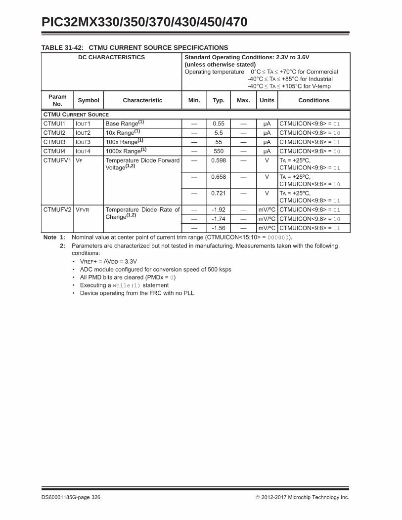
PIC32MX330/350/370/430/450/470
DS60001185G-page 326 2012-2017 Microchip Technology Inc.
TABLE 31-42: CTMU CURRENT SOURCE SPECIFICATIONSDC CHARACTERISTICS Standard Operating Conditions: 2.3V to 3.6V
(unless otherwise stated)Operating temperature 0°C TA +70°C for Commercial
-40°C TA +85°C for Industrial -40°C TA +105°C for V-temp
Param No. Symbol Characteristic Min. Typ. Max. Units Conditions
CTMU CURRENT SOURCE
CTMUI1 IOUT1 Base Range(1) — 0.55 — μA CTMUICON<9:8> = 01CTMUI2 IOUT2 10x Range(1) — 5.5 — μA CTMUICON<9:8> = 10CTMUI3 IOUT3 100x Range(1) — 55 — μA CTMUICON<9:8> = 11CTMUI4 IOUT4 1000x Range(1) — 550 — μA CTMUICON<9:8> = 00CTMUFV1 VF Temperature Diode Forward
Voltage(1,2)— 0.598 — V TA = +25ºC,
CTMUICON<9:8> = 01— 0.658 — V TA = +25ºC,
CTMUICON<9:8> = 10— 0.721 — V TA = +25ºC,
CTMUICON<9:8> = 11CTMUFV2 VFVR Temperature Diode Rate of
Change(1,2)— -1.92 — mV/ºC CTMUICON<9:8> = 01— -1.74 — mV/ºC CTMUICON<9:8> = 10— -1.56 — mV/ºC CTMUICON<9:8> = 11
Note 1: Nominal value at center point of current trim range (CTMUICON<15:10> = 000000).2: Parameters are characterized but not tested in manufacturing. Measurements taken with the following
conditions:• VREF+ = AVDD = 3.3V• ADC module configured for conversion speed of 500 ksps• All PMD bits are cleared (PMDx = 0)• Executing a while(1) statement• Device operating from the FRC with no PLL

2012-2017 Microchip Technology Inc. DS60001185G-page 327
PIC32MX330/350/370/430/450/470FIGURE 31-23: EJTAG TIMING CHARACTERISTICS
TTCKcycTTCKhigh TTCKlow
Trf
Trf
TrfTrf
TTsetup TThold
TTDOout TTDOzstate
Defined Undefined
TTRST*low
Trf
TCK
TDO
TRST*
TDI
TMS
TABLE 31-43: EJTAG TIMING REQUIREMENTS
AC CHARACTERISTICS
Standard Operating Conditions: 2.3V to 3.6V(unless otherwise stated)Operating temperature 0°C TA +70°C for Commercial
EJ1 TTCKCYC TCK Cycle Time 25 — ns —EJ2 TTCKHIGH TCK High Time 10 — ns —EJ3 TTCKLOW TCK Low Time 10 — ns —EJ4 TTSETUP TAP Signals Setup Time Before
Rising TCK5 — ns —
EJ5 TTHOLD TAP Signals Hold Time After Rising TCK
3 — ns —
EJ6 TTDOOUT TDO Output Delay Time from Falling TCK
— 5 ns —
EJ7 TTDOZSTATE TDO 3-State Delay Time from Falling TCK
— 5 ns —
EJ8 TTRSTLOW TRST Low Time 25 — ns —EJ9 TRF TAP Signals Rise/Fall Time, All
Input and Output— — ns —
Note 1: These parameters are characterized, but not tested in manufacturing.
-40°C TA +85°C for Industrial -40°C TA +105°C for V-temp
Param.No. Symbol Description(1) Min. Max. Units Conditions

PIC32MX330/350/370/430/450/470
DS60001185G-page 328 2012-2017 Microchip Technology Inc.
NOTES:

2012-2017 M
icrochip Technology Inc.D
S60001185G
-page
329
PIC32M
X330/350/370/430/450/470
32.0 DC AND AC DEVICE CHARACTERISTICS GRAPHSNote: The graphs provided following this note are a statistical summary based on a limited number of samples and are provided for design guidance purposes
only. The performance characteristics listed herein are not tested or guaranteed. In some graphs, the data presented may be outside the specified operating range (e.g., outside specified power supply range) and therefore, outside the warranted range.
FIGURE 32-1: VOH – 4x DRIVER PINS40.00
35.00
30.00
25.00
20.00
15.00Curren
t(mA)
10.00
5.00
0.000.0 0.5 1.0 1.5 2.0 2.5 3.0
Voltage (V)
3.3V
Absolute Maximum
FIGURE 32-2: VOH – 8x DRIVER PINS70.00
60.00
50.00
40.00
30.00
Curren
t(mA)
20.00
10.00
0.000.0 0.5 1.0 1.5 2.0 2.5 3.0
Voltage (V)
3.3V
Absolute Maximum
FIGURE 32-3: VOL – 4x DRIVER PINS
15.000
20.000
25.000
30.000
35.000
40.000
45.000
Curren
t(mA)
0.000
5.000
10.000
0.000 0.500 1.000 1.500 2.000 2.500 3.000
Voltage (V)
3.3V
Absolute Maximum
FIGURE 32-4: VOL – 8x DRIVER PINS
30.000
40.000
50.000
60.000
70.000
80.000
Curren
t(mA)
0.000
10.000
20.000
0.000 0.500 1.000 1.500 2.000 2.500 3.000
Voltage (V)
3.3V
Absolute Maximum

PIC32M
X330/350/370/430/450/470
DS
60001185G-page
330
2012-2017 M
icrochip Technology Inc.
FIGURE 32-5: TYPICAL IPD CURRENT @ VDD = 3.3V
PIC32MX330/430 DEVICES
150
200
250
300
350
400
IPD(μA)
0
50
100
150
40 30 20 10 0 10 20 30 40 50 60 70 80 90 100 110
Temperature (Celsius)
FIGURE 32-6: TYPICAL IPD CURRENT @ VDD = 3.3V
PIC32MX350/450 DEVICES
200
250
300
350
400
450
500
IPD(μA)
0
50
100
150
40 30 20 10 0 10 20 30 40 50 60 70 80 90 100 110
Temperature (Celsius)
FIGURE 32-7: TYPICAL IPD CURRENT @ VDD = 3.3V
PIC32MX350/450 DEVICES
250
300
350
400
450
500
550
600
IPD(μA)
0
50
100
150
200
40 30 20 10 0 10 20 30 40 50 60 70 80 90 100 110
Temperature (Celsius)
FIGURE 32-8: TYPICAL IIDLE CURRENT @ VDD = 3.3V
PIC32MX330/430 DEVICES
8
10
12
14
16
18
20
CURR
ENT(m
A)
0
2
4
6
0 10 20 30 40 50 60 70 80 90 100
IIDLE
MIPS

2012-2017 M
icrochip Technology Inc.D
S60001185G
-page
331
PIC32M
X330/350/370/430/450/470
FIGURE 32-9: TYPICAL IIDLE CURRENT @ VDD = 3.3V
PIC32MX350/450 DEVICES
8
10
12
14
16
18
20
CURR
ENT(m
A)
0
2
4
6
0 10 20 30 40 50 60 70 80 90 100
IIDLE
MIPS
FIGURE 32-10: TYPICAL IIDLE CURRENT @ VDD = 3.3V
PIC32MX370/470 DEVICES
8
10
12
14
16
18
20
CURR
ENT(m
A)
0
2
4
6
0 10 20 30 40 50 60 70 80 90 100
IIDLE
MIPS
FIGURE 32-11: TYPICAL IDD CURRENT @ VDD = 3.3V
PIC32MX330/430 DEVICES
30
40
50
60
IDD(m
A)
0
10
20
0 10 20 30 40 50 60 70 80 90 100
MIPS
FIGURE 32-12: TYPICAL IDD CURRENT @ VDD = 3.3V
PIC32MX350/450 DEVICES
30
40
50
60
IDD(m
A)
0
10
20
0 10 20 30 40 50 60 70 80 90 100
MIPS

PIC32M
X330/350/370/430/450/470
DS
60001185G-page
332
2012-2017 M
icrochip Technology Inc.
FIGURE 32-13: TYPICAL IDD CURRENT @ VDD = 3.3V
PIC32MX370/470 DEVICES
30
40
50
60
IDD(m
A)
0
10
20
0 10 20 30 40 50 60 70 80 90 100
MIPS
FIGURE 32-14: TYPICAL FRC FREQUENCY @ VDD = 3.3V
7930
7940
7950
7960
7970
7980
7990
8000
FRC
Fre
quen
cy (k
Hz)
7900
7910
7920
7930
7940
7950
7960
7970
7980
7990
8000
-40 -30 -20 -10 0 10 20 30 40 50 60 70 80 90 100
FRC
Fre
quen
cy (k
Hz)
Temperature (Celsius)
FIGURE 32-15: TYPICAL LPRC FREQUENCY @ VDD = 3.3V
31
32
33
LPR
C F
requ
ency
(kH
z)
30
31
32
33
-40 -30 -20 -10 0 10 20 30 40 50 60 70 80 90 100
LPR
C F
requ
ency
(kH
z)
Temperature (Celsius)
FIGURE 32-16: TYPICAL CTMU TEMPERATURE DIODE FORWARD VOLTAGE
0 500
0.550
0.600
0.650
0.700
0.750
0.800
0.850
Forw
ard
Volta
ge (V
)
0.350
0.400
0.450
0.500
0.550
0.600
0.650
0.700
0.750
0.800
0.850
-40 -30 -20 -10 0 10 20 30 40 50 60 70 80 90 100 110
Forw
ard
Volta
ge (V
)
Temperature (Celsius)
VF = 0.598
VF = 0.658
VF = 0.72155 μA, VFVR = -1.56 mV/ºC5.5 μA, VFVR = -1.74 mV/ºC0.55 μA, VFVR = -1.92 mV/ºC

2012-2017 Microchip Technology Inc. DS60001185G-page 333
PIC32MX330/350/370/430/450/47033.0 PACKAGING INFORMATION33.1 Package Marking Information
PIC32MX330F064H-I/PT
05100173e
Legend: XX...X Customer-specific information Y Year code (last digit of calendar year) YY Year code (last 2 digits of calendar year) WW Week code (week of January 1 is week ‘01’) NNN Alphanumeric traceability code Pb-free JEDEC designator for Matte Tin (Sn) * This package is Pb-free. The Pb-free JEDEC designator ( )
can be found on the outer packaging for this package.
Note: In the event the full Microchip part number cannot be marked on one line, it will be carried over to the next line, thus limiting the number of available characters for customer-specific information.
3e
64-Lead TQFP (10x10x1 mm)
XXXXXXXXXXXXXXXXXXXXXXXXXXXXXXYYWWNNN
Example
100-Lead TQFP (12x12x1 mm)
XXXXXXXXXXXXXXXXXXXXXXXXYYWWNNN
Example
PIC32MX330F064L-I/PT0510017
3e
100-Lead TQFP (14x14x1 mm)
XXXXXXXXXXXXXXXXXXXXXXXXYYWWNNN
Example
PIC32MX330F064L-I/PF0510017
3e

PIC32MX330/350/370/430/450/470
DS60001185G-page 334 2012-2017 Microchip Technology Inc.
33.1 Package Marking Information (Continued)
XXXXXXXXXX
124-Lead VTLA (9x9x0.9 mm)
XXXXXXXXXXXXXXXXXXXXYYWWNNN
PIC32MX430F
Example
064L-I/TL
05100173e
Legend: XX...X Customer-specific information Y Year code (last digit of calendar year) YY Year code (last 2 digits of calendar year) WW Week code (week of January 1 is week ‘01’) NNN Alphanumeric traceability code Pb-free JEDEC designator for Matte Tin (Sn) * This package is Pb-free. The Pb-free JEDEC designator ( )
can be found on the outer packaging for this package.
Note: In the event the full Microchip part number cannot be marked on one line, it will be carried over to the next line, thus limiting the number of available characters for customer-specific information.
3e
XXXXXXXXXX
64-Lead QFN (9x9x0.9 mm) with 5.40x5.40 Exposed Pad
XXXXXXXXXXXXXXXXXXXXYYWWNNN
PIC32MX330F
Example
128H-I/MR
05100173e
XXXXXXXXXX
64-Lead QFN (9x9x0.9 mm) with 4.7x4.7 Exposed Pad
XXXXXXXXXXXXXXXXXXXXYYWWNNN
PIC32MX330F
Example
064H-I/RG
05100173e

2012-2017 Microchip Technology Inc. DS60001185G-page 335
PIC32MX330/350/370/430/450/47033.2 Package Details The following sections give the technical details of the packages.
���������� ������������� ������������������ �!"#$����%���&
' ��(�� ������ �!"�����# $�% �&"� �'��� ���(�)"&�'"!&�) �����& #�*�&����&� ���&�� #��� ���� +��'% �!��&����� �!��� ��&�����,�!�- �'��� ������ ��' �!���!������#�.��#����&�����"# �'��#�%��!�������&�"!���!�����#�%��!�������&�"!���!�!�������&� $� #����/�''� ��!�# ��� ��' �!���������#�&�� �������� �����.�0���/��
1�+2 1�!�����' �!������� �� &������� $��&� ��" �!��*��*�&��"&�&�� ���� !��.32 � % � �� ���' �!���(�"!"�����*�&��"&�&�� ���� (�%�����%��'�&����"��! !������
' �( 3���&� �'�!&��"�� �&���4�� �#��*���!(�� �! �! �&� �������������4������� ��%���&��������& #��&��&&255***�'����������'5��4�����
6��&! ��77��.�.����' �!����7�'�&! ��8 89� ��:
8"') ���%�7 �#! 8 ;�7 �#���&�� ��/��1�+9 �����< ���& � = = �������# #����4�� �����4� !! �� ���/ ���� ���/�&��#�%%�� �� ���/ = ���/3��&�7 ��&� 7 ���/ ��;� ���/3��&���& 7� ������.33��&����� � �> ��/> �>9 �����?�#&� . ������1�+9 �����7 ��&� � ������1�+���# #����4�� �?�#&� .� ������1�+���# #����4�� �7 ��&� �� ������1�+7 �#�����4� !! � ���� = ����7 �#�?�#&� ) ���� ���� �������#����%&����� ��� � ��> ��> ��>���#����%&����� �1�&&�' � ��> ��> ��>
D
D1
E
E1
e
b
N
NOTE 1 1 2 3 NOTE 2
c
LA1
L1
A2
Aφ
β
α
�������� � �������� ���*��� +���@/1

PIC32MX330/350/370/430/450/470
DS60001185G-page 336 2012-2017 Microchip Technology Inc.
Note: For the most current package drawings, please see the Microchip Packaging Specification located at http://www.microchip.com/packaging

2012-2017 Microchip Technology Inc. DS60001185G-page 337
PIC32MX330/350/370/430/450/470
����������� ������������� ������������������ �!"#$����%���&
' ��(�� ������ �!"�����# $�% �&"� �'��� ���(�)"&�'"!&�) �����& #�*�&����&� ���&�� #��� ���� +��'% �!��&����� �!��� ��&�����,�!�- �'��� ������ ��' �!���!������#�.��#����&�����"# �'��#�%��!�������&�"!���!�����#�%��!�������&�"!���!�!�������&� $� #����/�''� ��!�# ��� ��' �!���������#�&�� �������� �����.�0���/��
1�+2 1�!�����' �!������� �� &������� $��&� ��" �!��*��*�&��"&�&�� ���� !��.32 � % � �� ���' �!���(�"!"�����*�&��"&�&�� ���� (�%�����%��'�&����"��! !������
' �( 3���&� �'�!&��"�� �&���4�� �#��*���!(�� �! �! �&� �������������4������� ��%���&��������& #��&��&&255***�'����������'5��4�����
6��&! ��77��.�.����' �!����7�'�&! ��8 89� ��:
8"') ���%�7 �#! 8 ���7 �#���&�� ��/��1�+9 �����< ���& � = = �������# #����4�� �����4� !! �� ���/ ���� ���/�&��#�%%�� �� ���/ = ���/3��&�7 ��&� 7 ���/ ��;� ���/3��&���& 7� ������.33��&����� � �> ��/> �>9 �����?�#&� . �;����1�+9 �����7 ��&� � �;����1�+���# #����4�� �?�#&� .� ������1�+���# #����4�� �7 ��&� �� ������1�+7 �#�����4� !! � ���� = ����7 �#�?�#&� ) ���� ���� �������#����%&����� ��� � ��> ��> ��>���#����%&����� �1�&&�' � ��> ��> ��>
D
D1
e
b
E1
E
N
NOTE 1 NOTE 21 23
c
LA1 L1
A2
A
φβ
α
�������� � �������� ���*��� +�����1

PIC32MX330/350/370/430/450/470
DS60001185G-page 338 2012-2017 Microchip Technology Inc.
Note: For the most current package drawings, please see the Microchip Packaging Specification located at http://www.microchip.com/packaging

2012-2017 Microchip Technology Inc. DS60001185G-page 339
PIC32MX330/350/370/430/450/470
����������� ������������� ���������#��#����� �!"#$����%���&
' ��(�� ������ �!"�����# $�% �&"� �'��� ���(�)"&�'"!&�) �����& #�*�&����&� ���&�� #��� ���� +��'% �!��&����� �!��� ��&�����,�!�- �'��� ������ ��' �!���!������#�.��#����&�����"# �'��#�%��!�������&�"!���!�����#�%��!�������&�"!���!�!�������&� $� #����/�''� ��!�# ��� ��' �!���������#�&�� �������� �����.�0���/��
1�+2 1�!�����' �!������� �� &������� $��&� ��" �!��*��*�&��"&�&�� ���� !��.32 � % � �� ���' �!���(�"!"�����*�&��"&�&�� ���� (�%�����%��'�&����"��! !������
' �( 3���&� �'�!&��"�� �&���4�� �#��*���!(�� �! �! �&� �������������4������� ��%���&��������& #��&��&&255***�'����������'5��4�����
6��&! ��77��.�.����' �!����7�'�&! ��8 89� ��:
8"') ���%�7 �#! 8 ���7 �#���&�� �����1�+9 �����< ���& � = = �������# #����4�� �����4� !! �� ���/ ���� ���/�&��#�%%�� �� ���/ = ���/3��&�7 ��&� 7 ���/ ��;� ���/3��&���& 7� ������.33��&����� � �> ��/> �>9 �����?�#&� . ������1�+9 �����7 ��&� � ������1�+���# #����4�� �?�#&� .� ������1�+���# #����4�� �7 ��&� �� ������1�+7 �#�����4� !! � ���� = ����7 �#�?�#&� ) ���� ���@ �������#����%&����� ��� � ��> ��> ��>���#����%&����� �1�&&�' � ��> ��> ��>
D
D1
E
E1
e
bN
123NOTE 1 NOTE 2
c
LA1
L1
A
A2
α
βφ
�������� � �������� ���*��� +�����1

PIC32MX330/350/370/430/450/470
DS60001185G-page 340 2012-2017 Microchip Technology Inc.
Note: For the most current package drawings, please see the Microchip Packaging Specification located at http://www.microchip.com/packaging

2012-2017 Microchip Technology Inc. DS60001185G-page 341
PIC32MX330/350/370/430/450/470
Note: For the most current package drawings, please see the Microchip Packaging Specification located at http://www.microchip.com/packaging

PIC32MX330/350/370/430/450/470
DS60001185G-page 342 2012-2017 Microchip Technology Inc.
Note: For the most current package drawings, please see the Microchip Packaging Specification located at http://www.microchip.com/packaging

2012-2017 Microchip Technology Inc. DS60001185G-page 343
PIC32MX330/350/370/430/450/470
For the most current package drawings, please see the Microchip Packaging Specification located athttp://www.microchip.com/packaging
Note:

PIC32MX330/350/370/430/450/470
DS60001185G-page 344 2012-2017 Microchip Technology Inc.
0.20 C
0.20 C
0.10 C A B0.05 C
(DATUM B)(DATUM A)
C
SEATING PLANE
12
2XTOP VIEW
SIDE VIEW
BOTTOM VIEW
For the most current package drawings, please see the Microchip Packaging Specification located athttp://www.microchip.com/packaging
Note:
NOTE 1
0.10 C
Microchip Technology Drawing C04-260A Sheet 1 of 2
2X
N
N
64X (K)
64X L
e2
0.10 C A B
0.10 C A B
NOTE 1
DETAIL A
64-Terminal Plastic Quad Flat Pack, No Lead (RG) 9x9x0.9 mm Body [QFN]Saw Singulated
BA
D2
E2
E
D
12
64X b
(A3)A
e

2012-2017 Microchip Technology Inc. DS60001185G-page 345
PIC32MX330/350/370/430/450/470
For the most current package drawings, please see the Microchip Packaging Specification located athttp://www.microchip.com/packaging
Note:
Number of Terminals
Overall Height
Terminal Width
Overall Width
Overall Length
Terminal Length
Exposed Pad Width
Exposed Pad Length
Pitch
Standoff
UnitsDimension Limits
A1A
b
DE2
D2
e
L
E
N0.50 BSC
4.60
0.300.15
0.800.00
0.200.40
4.70
0.850.02
9.00 BSC
MILLIMETERSMIN NOM
64
4.80
0.500.25
0.900.05
MAX
K 1.755 REF
REF: Reference Dimension, usually without tolerance, for information purposes only.BSC: Basic Dimension. Theoretically exact value shown without tolerances.
1.2.3.
Notes:
Pin 1 visual index feature may vary, but must be located within the hatched area.Package is saw singulatedDimensioning and tolerancing per ASME Y14.5M
Terminal-to-Exposed-Pad
0.08 C64X
DETAIL A
Microchip Technology Drawing C04-260A Sheet 2 of 2
64-Terminal Plastic Quad Flat Pack, No Lead (RG) 9x9x0.9 mm Body [QFN]Saw Singulated
4.60 4.709.00 BSC
4.80
C
SEATING PLANE
A1
Standoff A3 0.20 REF

PIC32MX330/350/370/430/450/470
DS60001185G-page 346 2012-2017 Microchip Technology Inc.
RECOMMENDED LAND PATTERN
For the most current package drawings, please see the Microchip Packaging Specification located athttp://www.microchip.com/packaging
Note:
Dimension LimitsUnits
C2
Optional Center Pad Width
Contact Pad Spacing
Optional Center Pad Length
Contact Pitch
Y2X2
4.804.80
MILLIMETERS
0.50 BSCMIN
EMAX
8.90
Contact Pad Length (X64)Contact Pad Width (X64)
Y1X1
0.850.25
BSC: Basic Dimension. Theoretically exact value shown without tolerances.
Notes:1. Dimensioning and tolerancing per ASME Y14.5M
Microchip Technology Drawing C04-2260A
NOM
C1Contact Pad Spacing 8.90
Contact Pad to Center Pad (X64) G1 1.625 REF
C1
C2
E
X2
Y2
64-Lead Very Thin Plastic Quad Flat, No Lead Package (RG) - 9x9x1.0 mm Body [QFN]4.7x4.7 mm Exposed Pad
Y1SILK SCREEN Y1
(G1)

2012-2017 Microchip Technology Inc. DS60001185G-page 347
PIC32MX330/350/370/430/450/470

PIC32MX330/350/370/430/450/470
DS60001185G-page 348 2012-2017 Microchip Technology Inc.

2012-2017 Microchip Technology Inc. DS60001185G-page 349
PIC32MX330/350/370/430/450/470
For the most current package drawings, please see the Microchip Packaging Specification located athttp://www.microchip.com/packaging
Note:
RECOMMENDED LAND PATTERN
SILK SCREEN
Dimension LimitsUnits
C1
Optional Center Pad Length
Contact Pad SpacingContact Pad Spacing
Optional Center Pad Chamfer (X4)
C2
W3W2
0.106.60
MILLIMETERSMIN MAX
8.508.50
Contact Pad Length (X124)Contact Pad Width (X124)
X2X1
0.300.30
BSC: Basic Dimension. Theoretically exact value shown without tolerances.
Notes:1. Dimensioning and tolerancing per ASME Y14.5M
Microchip Technology Drawing No. C04-2193A
NOM
Optional Center Pad Width T2Contact to Center Pad Clearance (X4) G5Pad Clearance G4Pad Clearance G3Pad Clearance G2
Contact Pitch 0.50 BSCEPad Clearance G1
6.600.300.200.200.200.20
EE/2
W2W3
G2
G4X1
G5X4
C2
C1
G3
G1
X2
E
T2
124-Very Thin Leadless Array Package (TL) – 9x9x0.9 mm Body [VTLA]

PIC32MX330/350/370/430/450/470
DS60001185G-page 350 2012-2017 Microchip Technology Inc.
NOTES:

2012-2017 Microchip Technology Inc. DS60001185G-page 351
PIC32MX330/350/370/430/450/470APPENDIX A: REVISION HISTORY
Revision A (July 2012)This is the initial released version of the document.
Revision B (April 2013)
Note: The status of this data sheet was updated to Preliminary; however, any electrical specifications listed for PIC32MX370/470 devices is to be considered Advance Information and is marked accordingly.
This revision includes the following updates, as shown in Table A-1.
TABLE A-1: MAJOR SECTION UPDATES Section Update Description
“32-bit Microcontrollers (up to 512 KB Flash and 128 KB SRAM) with Audio/Graphics/Touch (HMI), USB, and Advanced Analog”
SRAM was changed from 32 KB to 64 KB.
Data Memory (KB) was changed from 32 to 64 for the following devices (see Table 1):
• PIC32MX350F256H• PIC32MX350F256L• PIC32MX450F256H• PIC32MX450F256LThe following devices were added:
• PIC32MX370F512H• PIC32MX370F512L• PIC32MX470F512H• PIC32MX470F512L
4.0 “Memory Organization” The Memory Map for Devices with 256 KB of Program Memory was updated (see Figure 4-3).
The Memory Map for Devices with 512 KB of Program Memory was added (see Figure 4-4).
7.0 “Interrupt Controller” Updated the Interrupt IRQ, Vector and Bit Locations (see Table 7-1).
20.0 “Parallel Master Port (PMP)” Added the CS2 bit and updated the ADDR bits in the Parallel Port Address register (see Register 20-3).
27.0 “Special Features” Updated the PWP bit in the Device Configuration Word 3 register (see Register 27-4).
30.0 “Electrical Characteristics” Note 2 in the DC Characteristics: Operating Current (IDD) were updated (see Table 30-5).
Note 1 in the DC Characteristics: Idle Current (IIDLE) were updated (see Table 30-6).
Note 1 in the DC Characteristics: Power-down Current (IPD) were updated (see Table 30-7).
Updated Program Memory values for parameters D135 (TWW), D136 (TRW), and D137 (TPE and TCE) (see Table 30-12).
31.0 “DC and AC Device Characteristics Graphs”
New IDD, IIDLE, and IPD current graphs were added for PIC32MX330/430 devices and PIC32MX350/450 devices.

PIC32MX330/350/370/430/450/470
DS60001185G-page 352 2012-2017 Microchip Technology Inc.
Revision C (October 2013)This revision includes the following updates, as listed in Table A-2.
TABLE A-2: MAJOR SECTION UPDATES Section Update Description
“32-bit Microcontrollers (up to 512 KB Flash and 128 KB SRAM) with Audio/Graphics/Touch (HMI), USB, and Advanced Analog”
The Operating Conditions and Core sections were updated in support of 100 MHz (-40ºC to +85ºC) devices.
Added Notes 2 and 3 regarding the conductive thermal pad to the 124-pin VTLA pin diagrams.
2.0 “Guidelines for Getting Started with 32-bit MCUs”
Updated the recommended minimum connection (see Figure 2-1).
Added 2.10 “SOSC Design Recommendation”.
20.0 “Parallel Master Port (PMP)” Updated the Parallel Port Control register, PMCON (see Register 20-1).
Updated the Parallel Port Mode register, PMMODE (see Register 20-2).
Updated the Parallel Port Pin Enable register, PMAEN (see Register 20-4).
30.0 “Electrical Characteristics” Removed Note 4 from the Absolute Maximum Ratings.
The maximum frequency for parameter DC5 In Operating MIPS vs. Voltage was changed to 100 MHz (see Table 30-1).
Parameter DC25a was added to DC Characteristics: Operating Current (IDD) (see Table 30-5).
Parameter DC34c was added to DC Characteristics: Idle Current (IIDLE) (see Table 30-5).
Added parameters for PIC32MX370/470 devices and removed Note 5 from DC Characteristics: Power-Down Current (IPD) (see Table 30-7).
Updated the Minimum, Typical, and Maximum values and added a reference to Note 3 for parameter DI30 (ICNPU) in DC Characteristics: I/O Pin Input Specifications (see Table 30-8).
The SYSCLK values for all required Flash Wait states were updated (see Table 30-13).
Added parameter DO50A (CSOSC) to the Capacitive Loading Requirements on Output Pins (see Table 30-16).
Updated the maximum values for parameter OS10, and the Characteristics definition of parameter OS42 (GM) in the External Clock Timing Characteristics (see Table 30-17).
31.0 “DC and AC Device Characteristics Graphs”
Updated the IPD, IIDLE, and IDD graphs, and added new graphs for the PIC32MX370/470 devices (see Figure 31-5 through Figure 31-13).

2012-2017 Microchip Technology Inc. DS60001185G-page 353
PIC32MX330/350/370/430/450/470Revision D (March 2015)This revision includes the following updates, as listed in Table A-3.
TABLE A-3: MAJOR SECTION UPDATES Section Update Description
“32-bit Microcontrollers (up to 512 KB Flash and 128 KB SRAM) with Audio/Graphics/Touch (HMI), USB, and Advanced Analog”
100 MHz and 120 MHz operation information was added.
Pins 59 through 63 of the 64-pin QFN and TQFP pin diagrams were updated.
2.0 “Guidelines for Getting Started with 32-bit MCUs”
Added 2.8.1 “Crystal Oscillator Design Consideration”.
12.0 “I/O Ports” The Block Diagram of a Typical Multiplexed Port Structure was updated (see Figure 12-1).
21.0 “Parallel Master Port (PMP)”
The PMADDR: Parallel Port Address Register was updated (see Register 21-3).
31.0 “Electrical Characteristics”
Specifications for 120 MHz operation were added to the following tables:
• Table 31-1: “Operating MIPS vs. Voltage”• Table 31-5: “DC Characteristics: Operating Current (IDD)”• Table 31-6: “DC Characteristics: Idle Current (IIDLE)”• Table 31-7: “DC Characteristics: Idle Current (IPD)”• Table 31-13: “DC Characteristics: Program Flash Memory Wait State”• Table 31-18: “External Clock Timing Requirements”The unit of measure for IIDLE Current parameters DC37a, DC37b, and DC37c were updated (see Table 31-6).
Parameter D312 (TSET) was removed from the Comparator Specifications (see Table 31-14).
Comparator Voltage Reference Specifications were added (see Table 31-15).
Parameter OS10 (FOSC) in the External Clock Timing Requirements was updated (see Table 31-18).
Parameter USB321 (VOL) in the OTG Electrical Specifications was updated (see Table 31-41).
32.0 “Packaging Information” The 64-lead QFN package marking information was updated.
The 124-lead VTLA package land pattern information was added.
“Product Identification System” The Speed category was removed.
The Example was updated.
The MR package was updated.
The RG package was added.

PIC32MX330/350/370/430/450/470
DS60001185G-page 354 2012-2017 Microchip Technology Inc.
Revision E (October 2015)This revision includes the following updates, as listed in Table A-4.
Revision F (September 2016)This revision includes the following updates, as listed in Table A-5.
TABLE A-4: MAJOR SECTION UPDATES Section Update Description
2.0 “Guidelines for Getting Started with 32-bit MCUs”
Section 2.10 “Sosc Design Recommendations” was removed.
31.0 “Electrical Characteristics”
The Power-Down Current (IPD) DC Characteristics were updated (see Table 31-7).
TABLE A-5: MAJOR SECTION UPDATES Section Update Description
“32-bit Microcontrollers (up to 512 KB Flash and 128 KB SRAM) with Audio/Graphics/Touch (HMI), USB, and Advanced Analog”
The PIC32MX450F128HB and PIC32MX470F512LB devices and Note 4 were added to the family features table (see Table 1).
Note 2 in the 64-pin device pin table was updated (see Table 2).
Note 2 in the 64-pin device pin table was updated and Note 4 was removed (see Table 3).
Note 2 and Note 3 in the 100-pin device pin table was updated (see Table 4).
Note 3 in the 124-pin device pin table was updated (see Table 6).
Note 2 in the 124-pin device pin table was updated (see Table 7).
RPF3 was removed from USB devices (see Table 3, Table 5, and Table 7).
1.0 “Device Overview” The Pinout I/O Descriptions for pins U5CTS, U5RTS, U5RX, and U5TX in 64-pin QFN/TQFP packages were updated (see Table 1-1).
2.0 “Guidelines for Getting Started with 32-bit MCUs”
2.10 “EMI/EMC/EFT (IEC 61000-4-4 and IEC 61000-4-2) Suppression Considerations” was added.
8.0 “Oscillator Configuration”
The Clock Diagram was updated (see Figure 8-1).
The Center Frequency values in the TUN<5:0> bits (OSCTUN<5:0>) were updated (see Register 8-2).
12.0 “I/O Ports” Note references in the Input Pin Selection table were updated (see Table 12-1).
Note references in the Output Pin Selection table were updated (see Table 12-2).
PORTF Register Maps were updated (see Table 12-11 and Table 12-3).
Note 1 was added to the Peripheral Pin Select Input Register Map (see Table 12-17).
31.0 “Electrical Characteristics”
The conditions for parameter DI60b (IICH) were updated (see Table 31-8).
Parameter DO50a (CSOSC) was removed.
The maximum value for parameter OS10 (FOSC) was updated (see Table 31-18).
Parameter PM7 (TDHOLD) was updated (see Table 31-39).
Note 1 was added to the DC Characteristics: Program Memory (see Table 31-12).
33.0 “Packaging Information”
The Land Pattern for 64-pin QFN packages was updated.
“Product Identification System”
The Software Targeting category was added.

2012-2017 Microchip Technology Inc. DS60001185G-page 355
PIC32MX330/350/370/430/450/470Revision G (October 2017)This revision includes the following updates, as listed in Table A-6.
TABLE A-6: MAJOR SECTION UPDATES Section Update Description
“32-bit Microcontrollers (up to 512 KB Flash and 128 KB SRAM) with Audio/Graphics/Touch (HMI), USB, and Advanced Analog”
The PIC32MX450F128HB and PIC32MX470F512LB devices and Note 4 were removed (see Table 1).
“Product Identification System”
The Software Targeting category was removed.

PIC32MX330/350/370/430/450/470
DS60001185G-page 356 2012-2017 Microchip Technology Inc.
NOTES:

2012-2017 Microchip Technology Inc. DS60001185G-page 357
PIC32MX330/350/370/430/450/470INDEXAAC Characteristics ............................................................ 295
10-Bit Conversion Rate Parameters ......................... 318ADC Specifications ................................................... 316Analog-to-Digital Conversion Requirements............. 319EJTAG Timing Requirements ................................... 327Internal FRC Accuracy.............................................. 297Internal RC Accuracy ................................................ 298OTG Electrical Specifications ................................... 325Parallel Master Port Read Requirements ................. 323Parallel Master Port Write ......................................... 324Parallel Master Port Write Requirements.................. 324Parallel Slave Port Requirements ............................. 322PLL Clock Timing...................................................... 297
Analog-to-Digital Converter (ADC).................................... 233Assembler
MPASM Assembler................................................... 276
BBlock Diagrams
ADC Module.............................................................. 233Comparator I/O Operating Modes............................. 243Comparator Voltage Reference ................................ 247Connections for On-Chip Voltage Regulator............. 272CPU ............................................................................ 35CTMU Configurations
Time Measurement ........................................... 251DMA............................................................................ 93I2C Circuit ................................................................. 198Input Capture ............................................................ 181Interrupt Controller ...................................................... 63JTAG Programming, Debugging and Trace Ports .... 272Output Compare Module........................................... 185PMP Pinout and Connections to External Devices ... 213Prefetch Module.......................................................... 83Reset System.............................................................. 59RTCC........................................................................ 223SPI Module ............................................................... 189Timer1....................................................................... 167Timer2/3/4/5 (16-Bit) ................................................. 171Typical Multiplexed Port Structure .................... 137, 353UART ........................................................................ 205WDT and Power-up Timer ........................................ 177
Brown-out Reset (BOR)and On-Chip Voltage Regulator................................ 272
CC Compilers
MPLAB C18 .............................................................. 276Charge Time Measurement Unit. See CTMU.Clock Diagram .................................................................... 74Comparator
Specifications.................................................... 293, 294Comparator Module .......................................................... 243Comparator Voltage Reference (CVref ............................. 247Configuration Bit ............................................................... 261Configuring Analog Port Pins............................................ 138CPU
Architecture Overview................................................. 36Coprocessor 0 Registers ............................................ 37Core Exception Types................................................. 38EJTAG Debug Support ............................................... 38Power Management.................................................... 38
CPU Module ................................................................. 27, 35CTMU
Registers .................................................................. 253Customer Change Notification Service............................. 361Customer Notification Service .......................................... 361Customer Support............................................................. 361
DDC and AC Characteristics
Graphs and Tables ................................................... 329DC Characteristics............................................................ 280
I/O Pin Input Specifications ...................................... 287I/O Pin Output Specifications.................................... 290Idle Current (IIDLE) .................................................... 283Power-Down Current (IPD)........................................ 284Program Memory...................................................... 292Temperature and Voltage Specifications.................. 281
Development Support ....................................................... 275Direct Memory Access (DMA) Controller............................ 93
EElectrical Characteristics .................................................. 279
AC............................................................................. 295Errata .................................................................................. 14External Clock
Timer1 Timing Requirements ................................... 301Timer2, 3, 4, 5 Timing Requirements ....................... 302Timing Requirements ............................................... 296
FFlash Program Memory ...................................................... 53
RTSP Operation ......................................................... 53
HHigh Voltage Detect (HVD)................................. 61, 272, 291
II/O Ports............................................................................ 137
Parallel I/O (PIO) ...................................................... 138Write/Read Timing.................................................... 138
Input Change Notification ................................................. 138Instruction Set................................................................... 273Inter-Integrated Circuit (I2C .............................................. 197Internal Voltage Reference Specifications........................ 294Internet Address ............................................................... 361Interrupt Controller.............................................................. 63
IRG, Vector and Bit Location ...................................... 64
MMemory Maps
Devices with 128 KB of Program Memory.................. 41Devices with 256 KB of Program Memory.................. 42Devices with 512 KB of Program Memory.................. 43Devices with 64 KB of Program Memory.................... 40
Memory Organization ......................................................... 39Layout ......................................................................... 39
Microchip Internet Web Site.............................................. 361MPLAB ASM30 Assembler, Linker, Librarian ................... 276MPLAB Integrated Development Environment Software.. 275MPLAB PM3 Device Programmer .................................... 277MPLAB REAL ICE In-Circuit Emulator System ................ 277MPLINK Object Linker/MPLIB Object Librarian ................ 276

PIC32MX330/350/370/430/450/470
DS60001185G-page 358 2012-2017 Microchip Technology Inc.
OOscillator Configuration....................................................... 73Output Compare................................................................ 185
PPackaging ......................................................................... 333
Details ....................................................................... 335Marking ..................................................................... 333
Parallel Master Port (PMP) ............................................... 213PIC32 Family USB Interface Diagram............................... 114Pinout I/O Descriptions (table) ............................................ 18Power-on Reset (POR)
and On-Chip Voltage Regulator ................................ 272Power-Saving Features..................................................... 257
CPU Halted Methods ................................................ 257Operation .................................................................. 257with CPU Running..................................................... 257
Prefetch Cache ................................................................... 83
RReal-Time Clock and Calendar (RTCC)............................ 223Register Map
ADC .......................................................................... 235Bus Matrix ................................................................... 45Comparator ............................................................... 244Comparator Voltage Reference ................................ 248CTMU........................................................................ 252Device and Revision ID Summary ............................ 262Device Configuration Word Summary....................... 262DMA Channel 0-3 ....................................................... 95DMA CRC ................................................................... 94DMA Global................................................................. 94Flash Controller........................................................... 54I2C1 and I2C2........................................................... 199Interrupt....................................................................... 66Output Compare1-5 .................................................. 186Parallel Master Port .................................................. 214Peripheral Pin Select Input ....................................... 159Peripheral Pin Select Output..................................... 161PORTA...................................................................... 145PORTB...................................................................... 146PORTC ............................................................. 147, 148PORTD ............................................................. 149, 150PORTE.............................................................. 151, 152PORTF.............................................. 153, 154, 155, 156PORTG ............................................................. 157, 158Prefetch....................................................................... 84RTCC ........................................................................ 224SPI1 and SPI2 .......................................................... 190System Control ..................................................... 60, 75Timer1-5............................................................ 168, 173UART1-5 ................................................................... 206USB........................................................................... 115
Registers[pin name]R (Peripheral Pin Select Input)................. 165AD1CHS (ADC Input Select)..................................... 241AD1CON1 (A/D Control 1) ........................................ 232AD1CON1 (ADC Control 1)............................... 232, 237AD1CON2 (ADC Control 2)....................................... 239AD1CON3 (ADC Control 3)....................................... 240AD1CSSL (ADC Input Scan Select).......................... 242ALRMDATE (Alarm Date Value) ............................... 232ALRMDATECLR (ALRMDATE Clear)....................... 232ALRMDATESET (ALRMDATE Set) .......................... 232ALRMTIME (Alarm Time Value)................................ 231
ALRMTIMECLR (ALRMTIME Clear) ........................ 232ALRMTIMEINV (ALRMTIME Invert) ......................... 232ALRMTIMESET (ALRMTIME Set)............................ 232BMXBOOTSZ (Boot Flash (IFM) Size ........................ 51BMXCON (Bus Matrix Configuration) ......................... 46BMXDKPBA (Data RAM Kernel Program
Base Address) .................................................... 47BMXDRMSZ (Data RAM Size Register)..................... 50BMXDUDBA (Data RAM User Data Base Address)... 48BMXDUPBA (Data RAM User Program
Base Address) .................................................... 49BMXPFMSZ (Program Flash (PFM) Size).................. 51BMXPUPBA (Program Flash (PFM) User Program
Base Address) .................................................... 50CHEACC (Cache Access) .......................................... 86CHECON (Cache Control).......................................... 85CHEHIT (Cache Hit Statistics).................................... 91CHELRU (Cache LRU) ............................................... 90CHEMIS (Cache Miss Statistics) ................................ 91CHEMSK (Cache TAG Mask)..................................... 88CHETAG (Cache TAG)............................................... 87CHEW0 (Cache Word 0) ............................................ 88CHEW1 (Cache Word 1) ............................................ 89CHEW2 (Cache Word 2) ............................................ 89CHEW3 (Cache Word 3) ............................................ 90CM1CON (Comparator 1 Control) ............................ 245CMSTAT (Comparator Control Register).................. 246CNCONx (Change Notice Control for PORTx) ......... 166CTMUCON (CTMU Control) ..................................... 253CVRCON (Comparator Voltage Reference Control) 249DCHxCON (DMA Channel x Control) ....................... 103DCHxCPTR (DMA Channel x Cell Pointer) .............. 110DCHxCSIZ (DMA Channel x Cell-Size) .................... 110DCHxDAT (DMA Channel x Pattern Data) ............... 111DCHxDPTR (Channel x Destination Pointer) ........... 109DCHxDSA (DMA Channel x Destination
Start Address)................................................... 107DCHxDSIZ (DMA Channel x Destination Size) ........ 108DCHxECON (DMA Channel x Event Control) .......... 104DCHxINT (DMA Channel x Interrupt Control)........... 105DCHxSPTR (DMA Channel x Source Pointer) ......... 109DCHxSSA (DMA Channel x Source Start Address) . 107DCHxSSIZ (DMA Channel x Source Size) ............... 108DCRCCON (DMA CRC Control)............................... 100DCRCDATA (DMA CRC Data) ................................. 102DCRCXOR (DMA CRCXOR Enable) ....................... 102DEVCFG0 (Device Configuration Word 0................. 263DEVCFG1 (Device Configuration Word 1................. 265DEVCFG2 (Device Configuration Word 2................. 267DEVCFG3 (Device Configuration Word 3................. 269DEVID (Device and Revision ID) .............................. 271DMAADDR (DMA Address) ........................................ 99DMAADDR (DMR Address)........................................ 99DMACON (DMA Controller Control) ........................... 98DMASTAT (DMA Status) ............................................ 99I2CxCON (I2C Control)............................................. 200I2CxSTAT (I2C Status) ............................................. 202ICxCON (Input Capture x Control)............................ 182IFSx (Interrupt Flag Status) ........................................ 70INTCON (Interrupt Control)......................................... 68INTSTAT (Interrupt Status)......................................... 69IPCx (Interrupt Priority Control) .................................. 71IPTMR Interrupt Proximity Timer) ............................... 69NVMADDR (Flash Address) ....................................... 56NVMCON (Programming Control) .............................. 55

2012-2017 Microchip Technology Inc. DS60001185G-page 359
PIC32MX330/350/370/430/450/470NVMDATA (Flash Program Data)............................... 57NVMKEY (Programming Unlock)................................ 56NVMSRCADDR (Source Data Address)..................... 57OCxCON (Output Compare x Control) ..................... 187OSCCON (Oscillator Control) ..................................... 76PFABT (Prefetch Cache Abort Statistics) ................... 92PMADDR (Parallel Port Address) ............................. 219PMAEN (Parallel Port Pin Enable)............................ 220PMCON (Parallel Port Control) ................................. 215PMMODE (Parallel Port Mode)................................. 217PMSTAT (Parallel Port Status (Slave Modes Only).. 221REFOCON (Reference Oscillator Control) ................. 80REFOTRIM (Reference Oscillator Trim) ..................... 82RPnR (Peripheral Pin Select Output)........................ 165RSWRST (Software Reset) ........................................ 62RTCCON (RTC Control) ........................................... 225RTCDATE (RTC Date Value) ................................... 230RTCTIME (RTC Time Value) .................................... 229SPIxCON (SPI Control)............................................. 191SPIxCON2 (SPI Control 2)........................................ 194SPIxSTAT (SPI Status)............................................. 195T1CON (Type A Timer Control) ................................ 169TxCON (Type B Timer Control) ................................ 174U1ADDR (USB Address) .......................................... 131U1BDTP1 (USB BDT Page 1) .................................. 133U1BDTP2 (USB BDT Page 2) .................................. 134U1BDTP3 (USB BDT Page 3) .................................. 134U1CNFG1 (USB Configuration 1) ............................. 135U1CON (USB Control) .............................................. 129U1EIE (USB Error Interrupt Enable) ......................... 127U1EIR (USB Error Interrupt Status) .......................... 125U1EP0-U1EP15 (USB Endpoint Control) ................. 136U1FRMH (USB Frame Number High)....................... 132U1FRML (USB Frame Number Low) ........................ 131U1IE (USB Interrupt Enable)..................................... 124U1IR (USB Interrupt)................................................. 123U1OTGCON (USB OTG Control) ............................. 121U1OTGIE (USB OTG Interrupt Enable) .................... 119U1OTGIR (USB OTG Interrupt Status)..................... 118U1OTGSTAT (USB OTG Status).............................. 120U1PWRC (USB Power Control)................................ 122U1SOF (USB SOF Threshold).................................. 133U1STAT (USB Status) .............................................. 128U1TOK (USB Token) ................................................ 132WDTCON (Watchdog Timer Control) ....................... 179
Resets................................................................................. 59Revision History ................................................................ 351RTCALRM (RTC ALARM Control) .................................... 227
SSerial Peripheral Interface (SPI) ....................................... 189Software Simulator (MPLAB SIM)..................................... 277Special Features ............................................................... 261
TTimer1 Module.................................................................. 167Timer2/3, Timer4/5 Modules............................................. 171Timing Diagrams
10-Bit Analog-to-Digital Conversion (ASAM = 0, SSRC<2:0> = 000)........................ 320
10-Bit Analog-to-Digital Conversion (ASAM = 1, SSRC<2:0> = 111, SAMC<4:0> = 00001) ....... 321
EJTAG ...................................................................... 327External Clock .......................................................... 295I/O Characteristics .................................................... 298I2Cx Bus Data (Master Mode) .................................. 310I2Cx Bus Data (Slave Mode) .................................... 313I2Cx Bus Start/Stop Bits (Master Mode)................... 310I2Cx Bus Start/Stop Bits (Slave Mode)..................... 313Input Capture (CAPx) ............................................... 302OCx/PWM................................................................. 303Output Compare (OCx) ............................................ 303Parallel Master Port Read ........................................ 323Parallel Master Port Write......................................... 324Parallel Slave Port .................................................... 322SPIx Master Mode (CKE = 0) ................................... 304SPIx Master Mode (CKE = 1) ................................... 305SPIx Slave Mode (CKE = 0) ..................................... 306SPIx Slave Mode (CKE = 1) ..................................... 308Timer1, 2, 3, 4, 5 External Clock .............................. 301UART Reception....................................................... 212UART Transmission (8-bit or 9-bit Data) .................. 212
Timing RequirementsCLKO and I/O ........................................................... 298
Timing SpecificationsI2Cx Bus Data Requirements (Master Mode)........... 311I2Cx Bus Data Requirements (Slave Mode)............. 314Input Capture Requirements .................................... 302Output Compare Requirements................................ 303Simple OCx/PWM Mode Requirements ................... 303SPIx Master Mode (CKE = 0) Requirements............ 304SPIx Master Mode (CKE = 1) Requirements............ 305SPIx Slave Mode (CKE = 1) Requirements.............. 308SPIx Slave Mode Requirements (CKE = 0).............. 306
UUART................................................................................ 205USB On-The-Go (OTG) .................................................... 113
VVCAP pin............................................................................ 272Voltage Regulator (On-Chip) ............................................ 272
WWWW Address ................................................................. 361WWW, On-Line Support ..................................................... 14
PIC32MX330/350/370/430/450/470
DS60001185G-page 360 2012-2017 Microchip Technology Inc.
NOTES:

2012-2017 Microchip Technology Inc. DS60001185G-page 361
PIC32MX330/350/370/430/450/470
THE MICROCHIP WEB SITEMicrochip provides online support via our WWW site at www.microchip.com. This web site is used as a means to make files and information easily available to customers. Accessible by using your favorite Internet browser, the web site contains the following information:
• Product Support – Data sheets and errata, application notes and sample programs, design resources, user’s guides and hardware support documents, latest software releases and archived software
• General Technical Support – Frequently Asked Questions (FAQ), technical support requests, online discussion groups, Microchip consultant program member listing
• Business of Microchip – Product selector and ordering guides, latest Microchip press releases, listing of seminars and events, listings of Microchip sales offices, distributors and factory representatives
CUSTOMER CHANGE NOTIFICATION SERVICEMicrochip’s customer notification service helps keep customers current on Microchip products. Subscribers will receive e-mail notification whenever there are changes, updates, revisions or errata related to a specified product family or development tool of interest.
To register, access the Microchip web site at www.microchip.com. Under “Support”, click on “Customer Change Notification” and follow the registration instructions.
CUSTOMER SUPPORTUsers of Microchip products can receive assistance through several channels:
• Distributor or Representative• Local Sales Office• Field Application Engineer (FAE)• Technical Support
Customers should contact their distributor, representative or Field Application Engineer (FAE) for support. Local sales offices are also available to help customers. A listing of sales offices and locations is included in the back of this document.
Technical support is available through the web site at: http://microchip.com/support

2012-2017 Microchip Technology Inc. DS60001185G-page 362
PIC32MX330/350/370/430/450/470PRODUCT IDENTIFICATION SYSTEMTo order or obtain information, e.g., on pricing or delivery, refer to the factory or the listed sales office.
Architecture MX = 32-bit RISC MCU core
Product Groups 3XX = General purpose microcontroller family4XX = General purpose with USB microcontroller family
Flash Memory Family F = Flash program memory
Program Memory Size 064 = 6 4KB128 = 128KB256 = 256KB512 = 512KB
Pin Count H = 64-pinL = 100-pin
Speed blank = up to 100 MHz120 = up to 120 MHz
Temperature Range blank = 0°C to +70°C (Commercial)I = -40°C to +85°C (Industrial)V = -40°C to +105°C (V-Temp)
PackageMR = 64-Lead (9x9x0.9 mm) QFN with 5.40x5.40 Exposed Pad (Plastic Quad Flat)RG = 64-Lead (9x9x0.9 mm) QFN with 4.7x4.7 Exposed Pad (Plastic Quad Flat)PT = 64-Lead (10x10x1 mm) TQFP (Thin Quad Flatpack)PT = 100-Lead (12x12x1 mm) TQFP (Thin Quad Flatpack)PF = 100-Lead (14x14x1 mm) TQFP (Thin Quad Flatpack)TL = 124-Lead (9x9x0.9 mm) VTLA (Very Thin Leadless Array)
Pattern Three-digit QTP, SQTP, Code or Special Requirements (blank otherwise)ES = Engineering Sample
Example:PIC32MX330F064H-I/PT: General purpose PIC32, 32-bit RISC MCU, 64 KB program memory, 64-pin, Industrial temperature, TQFP package.
Microchip Brand
Architecture
Flash Memory Family
Pin Count
Product Groups
Program Memory Size (KB)
PIC32 MX 3XX F 064 H T - XXX I / PT - XXX
Flash Memory Family
Tape and Reel Flag (if applicable)
Pattern
Package
Temperature RangeSpeed

2012-2017 Microchip Technology Inc. DS60001185G-page 363
Information contained in this publication regarding device applications and the like is provided only for your convenience and may be superseded by updates. It is your responsibility to ensure that your application meets with your specifications. MICROCHIP MAKES NO REPRESENTATIONS OR WARRANTIES OF ANY KIND WHETHER EXPRESS OR IMPLIED, WRITTEN OR ORAL, STATUTORY OR OTHERWISE, RELATED TO THE INFORMATION, INCLUDING BUT NOT LIMITED TO ITS CONDITION, QUALITY, PERFORMANCE, MERCHANTABILITY OR FITNESS FOR PURPOSE. Microchip disclaims all liability arising from this information and its use. Use of Microchip devices in life support and/or safety applications is entirely at the buyer’s risk, and the buyer agrees to defend, indemnify and hold harmless Microchip from any and all damages, claims, suits, or expenses resulting from such use. No licenses are conveyed, implicitly or otherwise, under any Microchip intellectual property rights unless otherwise stated.
Trademarks
The Microchip name and logo, the Microchip logo, AnyRate, dsPIC, FlashFlex, flexPWR, Heldo, JukeBlox, KeeLoq, KeeLoq logo, Kleer, LANCheck, LINK MD, MediaLB, MOST, MOST logo, MPLAB, OptoLyzer, PIC, PICSTART, PIC32 logo, RightTouch, SpyNIC, SST, SST Logo, SuperFlash and UNI/O are registered trademarks of Microchip Technology Incorporated in the U.S.A. and other countries.
ClockWorks, The Embedded Control Solutions Company, ETHERSYNCH, Hyper Speed Control, HyperLight Load, IntelliMOS, mTouch, Precision Edge, and QUIET-WIRE are registered trademarks of Microchip Technology Incorporated in the U.S.A.
Analog-for-the-Digital Age, Any Capacitor, AnyIn, AnyOut, BodyCom, chipKIT, chipKIT logo, CodeGuard, dsPICDEM, dsPICDEM.net, Dynamic Average Matching, DAM, ECAN, EtherGREEN, In-Circuit Serial Programming, ICSP, Inter-Chip Connectivity, JitterBlocker, KleerNet, KleerNet logo, MiWi, motorBench, MPASM, MPF, MPLAB Certified logo, MPLIB, MPLINK, MultiTRAK, NetDetach, Omniscient Code Generation, PICDEM, PICDEM.net, PICkit, PICtail, PureSilicon, RightTouch logo, REAL ICE, Ripple Blocker, Serial Quad I/O, SQI, SuperSwitcher, SuperSwitcher II, Total Endurance, TSHARC, USBCheck, VariSense, ViewSpan, WiperLock, Wireless DNA, and ZENA are trademarks of Microchip Technology Incorporated in the U.S.A. and other countries.
SQTP is a service mark of Microchip Technology Incorporated in the U.S.A.
Silicon Storage Technology is a registered trademark of Microchip Technology Inc. in other countries.
GestIC is a registered trademarks of Microchip Technology Germany II GmbH & Co. KG, a subsidiary of Microchip Technology Inc., in other countries.
All other trademarks mentioned herein are property of their respective companies.
© 2012-2017, Microchip Technology Incorporated, Printed in the U.S.A., All Rights Reserved.
ISBN: 978-1-5224-2247-1
Note the following details of the code protection feature on Microchip devices:• Microchip products meet the specification contained in their particular Microchip Data Sheet.
• Microchip believes that its family of products is one of the most secure families of its kind on the market today, when used in the intended manner and under normal conditions.
• There are dishonest and possibly illegal methods used to breach the code protection feature. All of these methods, to our knowledge, require using the Microchip products in a manner outside the operating specifications contained in Microchip’s Data Sheets. Most likely, the person doing so is engaged in theft of intellectual property.
• Microchip is willing to work with the customer who is concerned about the integrity of their code.
• Neither Microchip nor any other semiconductor manufacturer can guarantee the security of their code. Code protection does not mean that we are guaranteeing the product as “unbreakable.”
Code protection is constantly evolving. We at Microchip are committed to continuously improving the code protection features of our products. Attempts to break Microchip’s code protection feature may be a violation of the Digital Millennium Copyright Act. If such acts allow unauthorized access to your software or other copyrighted work, you may have a right to sue for relief under that Act.
Microchip received ISO/TS-16949:2009 certification for its worldwide headquarters, design and wafer fabrication facilities in Chandler and Tempe, Arizona; Gresham, Oregon and design centers in California and India. The Company’s quality system processes and procedures are for its PIC® MCUs and dsPIC® DSCs, KEELOQ® code hopping devices, Serial EEPROMs, microperipherals, nonvolatile memory and analog products. In addition, Microchip’s quality system for the design and manufacture of development systems is ISO 9001:2000 certified.

DS60001185G-page 364 2017 Microchip Technology Inc.
AMERICASCorporate Office2355 West Chandler Blvd.Chandler, AZ 85224-6199Tel: 480-792-7200 Fax: 480-792-7277Technical Support: http://www.microchip.com/supportWeb Address: www.microchip.comAtlantaDuluth, GA Tel: 678-957-9614 Fax: 678-957-1455Austin, TXTel: 512-257-3370 BostonWestborough, MA Tel: 774-760-0087 Fax: 774-760-0088ChicagoItasca, IL Tel: 630-285-0071 Fax: 630-285-0075DallasAddison, TX Tel: 972-818-7423 Fax: 972-818-2924DetroitNovi, MI Tel: 248-848-4000Houston, TX Tel: 281-894-5983IndianapolisNoblesville, IN Tel: 317-773-8323Fax: 317-773-5453Tel: 317-536-2380Los AngelesMission Viejo, CA Tel: 949-462-9523Fax: 949-462-9608Tel: 951-273-7800 Raleigh, NC Tel: 919-844-7510New York, NY Tel: 631-435-6000San Jose, CA Tel: 408-735-9110Tel: 408-436-4270Canada - TorontoTel: 905-695-1980 Fax: 905-695-2078
ASIA/PACIFICAsia Pacific OfficeSuites 3707-14, 37th FloorTower 6, The GatewayHarbour City, KowloonHong KongTel: 852-2943-5100Fax: 852-2401-3431Australia - SydneyTel: 61-2-9868-6733Fax: 61-2-9868-6755China - BeijingTel: 86-10-8569-7000 Fax: 86-10-8528-2104China - ChengduTel: 86-28-8665-5511Fax: 86-28-8665-7889China - ChongqingTel: 86-23-8980-9588Fax: 86-23-8980-9500China - DongguanTel: 86-769-8702-9880 China - GuangzhouTel: 86-20-8755-8029 China - HangzhouTel: 86-571-8792-8115 Fax: 86-571-8792-8116China - Hong Kong SARTel: 852-2943-5100 Fax: 852-2401-3431China - NanjingTel: 86-25-8473-2460Fax: 86-25-8473-2470China - QingdaoTel: 86-532-8502-7355Fax: 86-532-8502-7205China - ShanghaiTel: 86-21-3326-8000 Fax: 86-21-3326-8021China - ShenyangTel: 86-24-2334-2829Fax: 86-24-2334-2393China - ShenzhenTel: 86-755-8864-2200 Fax: 86-755-8203-1760China - WuhanTel: 86-27-5980-5300Fax: 86-27-5980-5118China - XianTel: 86-29-8833-7252Fax: 86-29-8833-7256
ASIA/PACIFICChina - XiamenTel: 86-592-2388138 Fax: 86-592-2388130China - ZhuhaiTel: 86-756-3210040 Fax: 86-756-3210049India - BangaloreTel: 91-80-3090-4444 Fax: 91-80-3090-4123India - New DelhiTel: 91-11-4160-8631Fax: 91-11-4160-8632India - PuneTel: 91-20-3019-1500Japan - OsakaTel: 81-6-6152-7160 Fax: 81-6-6152-9310Japan - TokyoTel: 81-3-6880- 3770 Fax: 81-3-6880-3771Korea - DaeguTel: 82-53-744-4301Fax: 82-53-744-4302Korea - SeoulTel: 82-2-554-7200Fax: 82-2-558-5932 or 82-2-558-5934Malaysia - Kuala LumpurTel: 60-3-6201-9857Fax: 60-3-6201-9859Malaysia - PenangTel: 60-4-227-8870Fax: 60-4-227-4068Philippines - ManilaTel: 63-2-634-9065Fax: 63-2-634-9069SingaporeTel: 65-6334-8870Fax: 65-6334-8850Taiwan - Hsin ChuTel: 886-3-5778-366Fax: 886-3-5770-955Taiwan - KaohsiungTel: 886-7-213-7830Taiwan - TaipeiTel: 886-2-2508-8600 Fax: 886-2-2508-0102Thailand - BangkokTel: 66-2-694-1351Fax: 66-2-694-1350
EUROPEAustria - WelsTel: 43-7242-2244-39Fax: 43-7242-2244-393Denmark - CopenhagenTel: 45-4450-2828 Fax: 45-4485-2829Finland - EspooTel: 358-9-4520-820France - ParisTel: 33-1-69-53-63-20 Fax: 33-1-69-30-90-79 Germany - GarchingTel: 49-8931-9700Germany - HaanTel: 49-2129-3766400Germany - HeilbronnTel: 49-7131-67-3636Germany - KarlsruheTel: 49-721-625370Germany - MunichTel: 49-89-627-144-0 Fax: 49-89-627-144-44Germany - RosenheimTel: 49-8031-354-560Israel - Ra’anana Tel: 972-9-744-7705Italy - Milan Tel: 39-0331-742611 Fax: 39-0331-466781Italy - PadovaTel: 39-049-7625286 Netherlands - DrunenTel: 31-416-690399 Fax: 31-416-690340Norway - TrondheimTel: 47-7289-7561Poland - WarsawTel: 48-22-3325737 Romania - BucharestTel: 40-21-407-87-50Spain - MadridTel: 34-91-708-08-90Fax: 34-91-708-08-91Sweden - GothenbergTel: 46-31-704-60-40Sweden - StockholmTel: 46-8-5090-4654UK - WokinghamTel: 44-118-921-5800Fax: 44-118-921-5820
Worldwide Sales and Service
10/10/17