Embed Size (px)
Citation preview
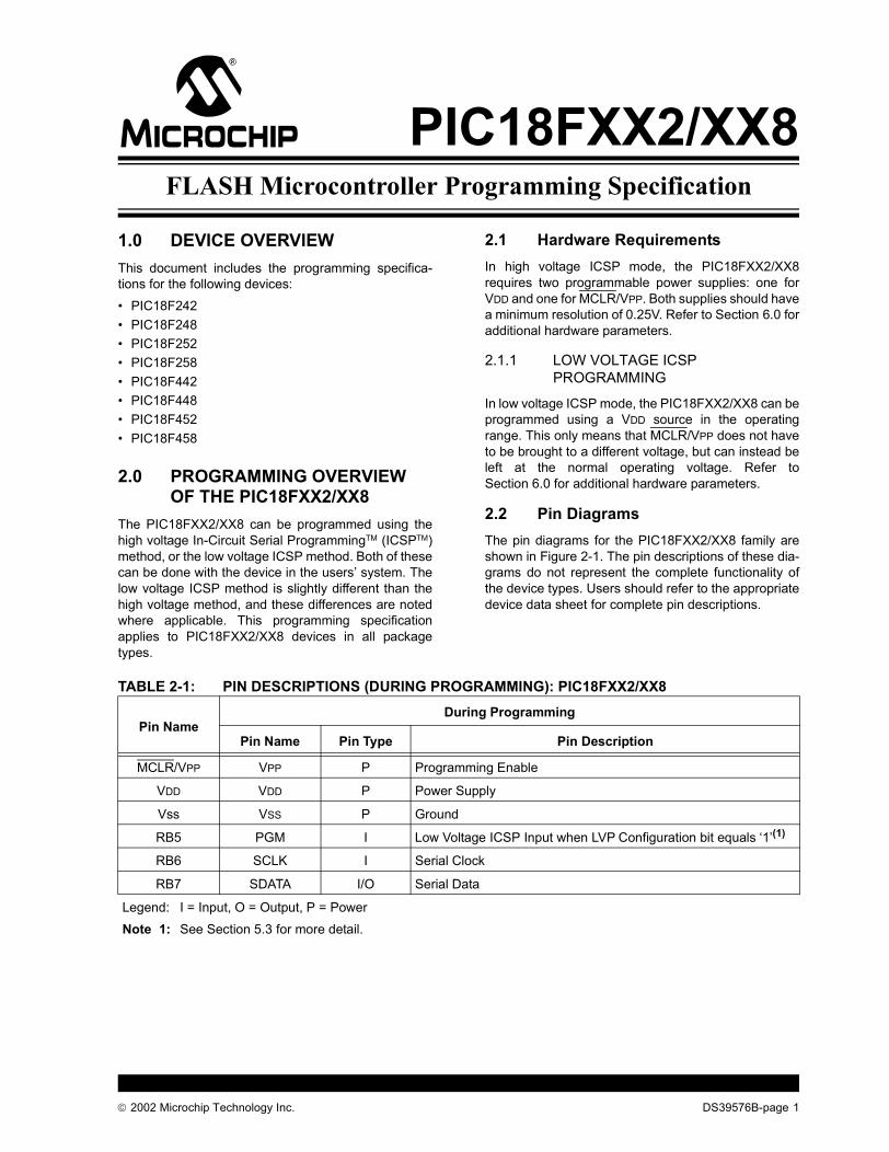
PIC18FXX2/XX8FLASH Microcontroller Programming Specification
1.0 DEVICE OVERVIEWThis document includes the programming specifica-tions for the following devices:
• PIC18F242• PIC18F248• PIC18F252• PIC18F258• PIC18F442• PIC18F448• PIC18F452• PIC18F458
2.0 PROGRAMMING OVERVIEW OF THE PIC18FXX2/XX8
The PIC18FXX2/XX8 can be programmed using thehigh voltage In-Circuit Serial ProgrammingTM (ICSPTM)method, or the low voltage ICSP method. Both of thesecan be done with the device in the users’ system. Thelow voltage ICSP method is slightly different than thehigh voltage method, and these differences are notedwhere applicable. This programming specificationapplies to PIC18FXX2/XX8 devices in all packagetypes.
2.1 Hardware RequirementsIn high voltage ICSP mode, the PIC18FXX2/XX8requires two programmable power supplies: one forVDD and one for MCLR/VPP. Both supplies should havea minimum resolution of 0.25V. Refer to Section 6.0 foradditional hardware parameters.
2.1.1 LOW VOLTAGE ICSP PROGRAMMING
In low voltage ICSP mode, the PIC18FXX2/XX8 can beprogrammed using a VDD source in the operatingrange. This only means that MCLR/VPP does not haveto be brought to a different voltage, but can instead beleft at the normal operating voltage. Refer toSection 6.0 for additional hardware parameters.
2.2 Pin DiagramsThe pin diagrams for the PIC18FXX2/XX8 family areshown in Figure 2-1. The pin descriptions of these dia-grams do not represent the complete functionality ofthe device types. Users should refer to the appropriatedevice data sheet for complete pin descriptions.
TABLE 2-1: PIN DESCRIPTIONS (DURING PROGRAMMING): PIC18FXX2/XX8
Pin NameDuring Programming
Pin Name Pin Type Pin Description
MCLR/VPP VPP P Programming Enable
VDD VDD P Power Supply
Vss VSS P Ground
RB5 PGM I Low Voltage ICSP Input when LVP Configuration bit equals ‘1’(1)
RB6 SCLK I Serial Clock
RB7 SDATA I/O Serial Data
Legend: I = Input, O = Output, P = Power
Note 1: See Section 5.3 for more detail.
2002 Microchip Technology Inc. DS39576B-page 1

PIC18FXX2/XX8
FIGURE 2-1: PIC18FXX2/XX8 FAMILY PIN DIAGRAMSNote: Not all multiplexed pin definitions are shown. Refer to the appropriate data sheet for complete pin descriptions.
101112131415161718 19 20 21 22 23 24 25 26
44
87
6 5 4 3 2 1
27 28 293031323334353637383940414243
9 PIC18F4X2
RA4RA5RE0
OSC2
NC
RE1RE2VDD
OSC1
RB3RB2RB1RB0VDDVSSRD7RD6RD5RD4RC7
RA3
RA2
RA1
RA0
MC
LR/V
PP
NC
RB7
RB6
RB5
RB4
NC
NC
RC
6R
C5
RC
4R
D3
RD
2R
D1
RD
0R
C3
RC
2R
C1
VSS
RC0
PIC18F4X8
44L PLCC
1011
23456
1
18 19 20 21 2212 13 14 15
38
87
44 43 42 41 40 39
16 17
2930313233
232425262728
36 3435
9
37
RA
3R
A2
RA
1R
A0
MC
LR/V
PP
NC
RB
7R
B6
RB
5R
B4
NC
RC
6R
C5
RC
4R
D3
RD
2R
D1
RD
0R
C3
RC
2R
C1
NC
NCRC0OSC2OSC1VSSVDDRE2RE1RE0RA5RA4
RC7RD4RD5RD6RD7VSSVDDRB0RB1RB2RB3
PIC18F4X2PIC18F4X8
44L QFP
RB7RB6RB5RB4RB3RB2RB1RB0VDD
VSS
RD7RD6RD5RD4RC7RC6RC5RC4RD3RD2
MCLR/VPPRA0RA1RA2RA3RA4RA5RE0RE1RE2VDDVSS
OSC1OSC2
RC0RC1RC2RC3RD0RD1
12345678
1011121314151617181920
4039383736353433323130292827262524232221
PIC
18F4
X2/8
40L
DIP
9
MCLR/VPPRA0RA1RA2RA3RA4RA5VSS
OSC1OSC2
RC0RC1RC2RC3
RB7RB6RB5RB4RB3RB2RB1RB0VDD
VSS
RC7RC6RC5RC4
12345678
1011121314
2827262524232221201918171615
9
PIC
18F2
X2/8
28L
DIP
PIC
18F2
X2/8
28L
SO
IC
1011
23456
1
18 19 20 21 2212 13 14 15
38
87
44 43 42 41 40 39
16 17
2930313233
232425262728
36 3435
9
37
RA
3R
A2
RA
1R
A0
MC
LR/V
PP
RB
3
RB
7R
B6
RB
5R
B4
NC
RC
6R
C5
RC
4R
D3
RD
2R
D1
RD
0R
C3
RC
2R
C1
RC
0
OSC2OSC1VSS
VDD
RE2RE1RE0RA5RA4
RC7RD4RD5RD6RD7VSSVDD
RB0RB1RB2
PIC18F4X2 AVSS
VDD
AVDD
PIC18F4X8
44L QFN
DS39576B-page 2 2002 Microchip Technology Inc.

PIC18FXX2/XX8
2.3 Memory MapThe code memory space extends from 0000h to 7FFFh(32 Kbytes) in four, 8-Kbyte panels. Addresses 0000hthrough 01FFh, however, define a “Boot Block” regionthat is treated separately from Panel 1. All codememory is on-chip.In addition to the code memory space, there are threeblocks in the configuration and ID space that are acces-sible to the user through Table Reads and Table Writes.Their locations in the memory map are shown inFigure 2-3.
TABLE 2-2: IMPLEMENTATION OF CODE MEMORY
FIGURE 2-2: CODE MEMORY SPACE FOR PIC18FXX2/XX8 DEVICES
Device Code Memory Size (Bytes)
PIC18F2420000h - 3FFFh (16K)
PIC18F248PIC18F252
0000h - 7FFFh (32K)PIC18F258PIC18F442
0000h - 3FFFh (16K)PIC18F448PIC18F452
0000h - 7FFFh (32K)PIC18F458
MEMORY SIZE / DEVICE Block Code Protection
Controlled By:16 Kbytes(PIC18FX42)
32 Kbytes(PIC18FX52)
Address Range
Boot Block Boot Block 000000h0001FFh CPB, WRTB, EBTRB
Block 0 Block 0000200h
001FFFhCP0, WRT0, EBTR0
Block 1 Block 1002000h
003FFFhCP1, WRT1, EBTR1
UnimplementedRead ‘0’s Block 2
004000h
005FFFhCP2, WRT2, EBTR2
UnimplementedRead ‘0’s Block 3
006000h
007FFFhCP3, WRT3, EBTR3
UnimplementedRead ‘0’s
UnimplementedRead ‘0’s
008000h
1FFFFFh
(Unimplemented Memory Space)
2002 Microchip Technology Inc. DS39576B-page 3
PIC18FXX2/XX8
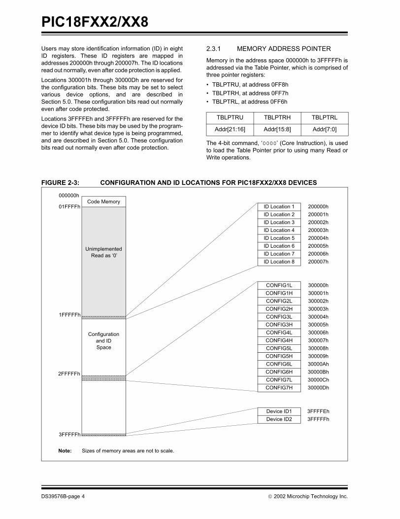
Users may store identification information (ID) in eightID registers. These ID registers are mapped inaddresses 200000h through 200007h. The ID locationsread out normally, even after code protection is applied.Locations 300001h through 30000Dh are reserved forthe configuration bits. These bits may be set to selectvarious device options, and are described inSection 5.0. These configuration bits read out normallyeven after code protected.
Locations 3FFFFEh and 3FFFFFh are reserved for thedevice ID bits. These bits may be used by the program-mer to identify what device type is being programmed,and are described in Section 5.0. These configurationbits read out normally even after code protection.
2.3.1 MEMORY ADDRESS POINTER
Memory in the address space 000000h to 3FFFFFh isaddressed via the Table Pointer, which is comprised ofthree pointer registers:
• TBLPTRU, at address 0FF8h• TBLPTRH, at address 0FF7h• TBLPTRL, at address 0FF6h
The 4-bit command, ‘0000’ (Core Instruction), is usedto load the Table Pointer prior to using many Read orWrite operations.
FIGURE 2-3: CONFIGURATION AND ID LOCATIONS FOR PIC18FXX2/XX8 DEVICES
TBLPTRU TBLPTRH TBLPTRL
Addr[21:16] Addr[15:8] Addr[7:0]
ID Location 1 200000hID Location 2 200001hID Location 3 200002hID Location 4 200003hID Location 5 200004hID Location 6 200005hID Location 7 200006hID Location 8 200007h
CONFIG1L 300000hCONFIG1H 300001hCONFIG2L 300002hCONFIG2H 300003hCONFIG3L 300004hCONFIG3H 300005hCONFIG4L 300006hCONFIG4H 300007hCONFIG5L 300008hCONFIG5H 300009hCONFIG6L 30000AhCONFIG6H 30000BhCONFIG7L 30000ChCONFIG7H 30000Dh
Device ID1 3FFFFEhDevice ID2 3FFFFFh
Note: Sizes of memory areas are not to scale.
000000h
1FFFFFh
3FFFFFh
01FFFFhCode Memory
UnimplementedRead as ‘0’
Configurationand IDSpace
2FFFFFh
DS39576B-page 4 2002 Microchip Technology Inc.
PIC18FXX2/XX8
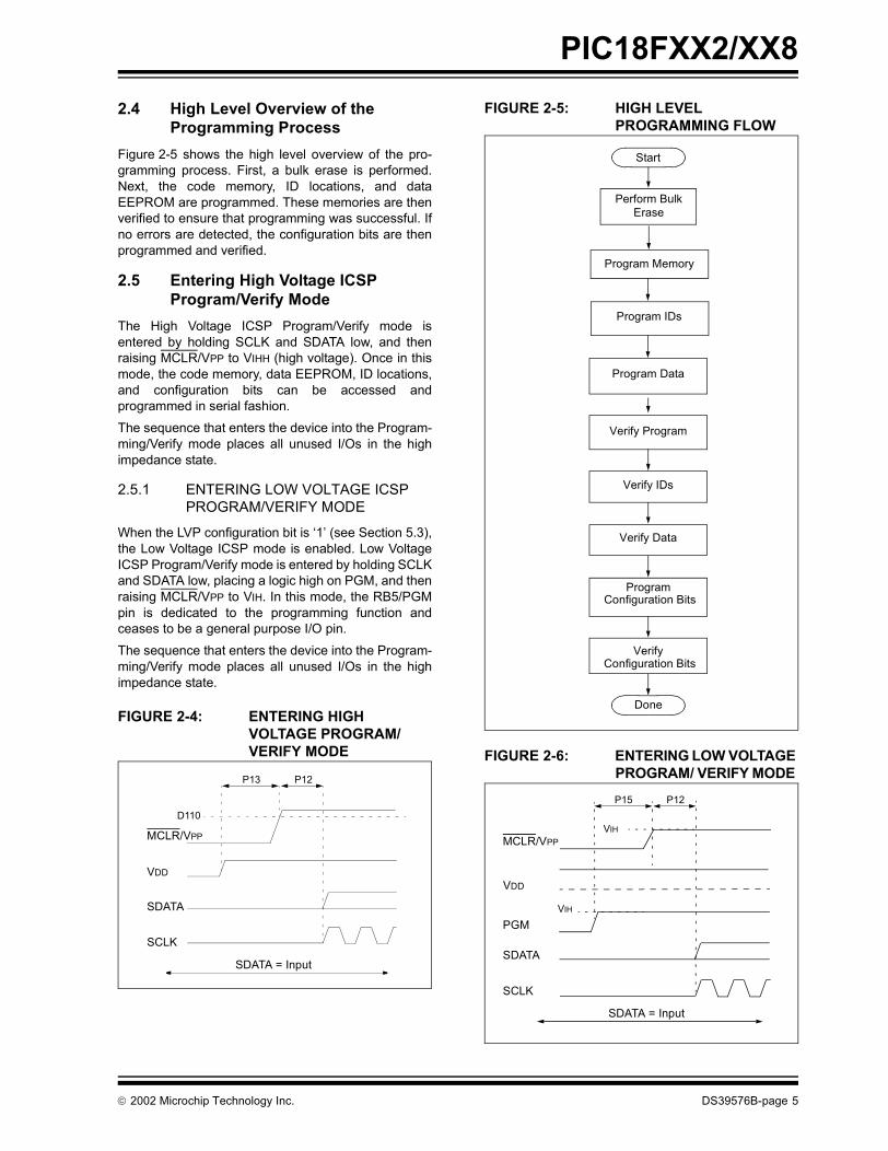
2.4 High Level Overview of theProgramming ProcessFigure 2-5 shows the high level overview of the pro-gramming process. First, a bulk erase is performed.Next, the code memory, ID locations, and dataEEPROM are programmed. These memories are thenverified to ensure that programming was successful. Ifno errors are detected, the configuration bits are thenprogrammed and verified.
2.5 Entering High Voltage ICSP Program/Verify Mode
The High Voltage ICSP Program/Verify mode isentered by holding SCLK and SDATA low, and thenraising MCLR/VPP to VIHH (high voltage). Once in thismode, the code memory, data EEPROM, ID locations,and configuration bits can be accessed andprogrammed in serial fashion.
The sequence that enters the device into the Program-ming/Verify mode places all unused I/Os in the highimpedance state.
2.5.1 ENTERING LOW VOLTAGE ICSP PROGRAM/VERIFY MODE
When the LVP configuration bit is ‘1’ (see Section 5.3),the Low Voltage ICSP mode is enabled. Low VoltageICSP Program/Verify mode is entered by holding SCLKand SDATA low, placing a logic high on PGM, and thenraising MCLR/VPP to VIH. In this mode, the RB5/PGMpin is dedicated to the programming function andceases to be a general purpose I/O pin.
The sequence that enters the device into the Program-ming/Verify mode places all unused I/Os in the highimpedance state.
FIGURE 2-4: ENTERING HIGH VOLTAGE PROGRAM/ VERIFY MODE
FIGURE 2-5: HIGH LEVEL PROGRAMMING FLOW
FIGURE 2-6: ENTERING LOW VOLTAGE PROGRAM/ VERIFY MODE
MCLR/VPP
P12
SDATA
SDATA = Input
SCLK
VDD
D110
P13
Start
Program Memory
Program IDs
Program Data
Verify Program
Verify IDs
Verify Data
Program Configuration Bits
Verify Configuration Bits
Done
Perform BulkErase
MCLR/VPP
P12
SDATA
SDATA = Input
SCLK
PGM
P15
VDD
VIH
VIH
2002 Microchip Technology Inc. DS39576B-page 5

PIC18FXX2/XX8
2.6 Serial Program/Verify OperationThe SCLK pin is used as a clock input pin and theSDATA pin is used for entering command bits and datainput/output during serial operation. Commands anddata are transmitted on the rising edge of SCLK,latched on the falling edge of SCLK, and are LeastSignificant bit (LSb) first.2.6.1 4-BIT COMMANDS
All instructions are 20 bits, consisting of a leading 4-bitcommand followed by a 16-bit operand, which dependson the type of command being executed. To input acommand, SCLK is cycled four times. The commandsneeded for programming and verification are shown inTable 2-3.
Depending on the 4-bit command, the 16-bit operandrepresents 16 bits of input data or 8 bits of input dataand 8 bits of output data.
Throughout this specification, commands and data arepresented as illustrated in Figure 2-4. The 4-bit com-mand is shown MSb first. The command operand, or“Data Payload”, is shown <MSB><LSB>. Figure 2-7demonstrates how to serially present a 20-bitcommand/operand to the device.
2.6.2 CORE INSTRUCTION
The core instruction passes a 16-bit instruction to theCPU core for execution. This is needed to setupregisters as appropriate for use with other commands.
TABLE 2-3: COMMANDS FOR PROGRAMMING
TABLE 2-4: SAMPLE COMMAND SEQUENCE
FIGURE 2-7: TABLE WRITE, POST INCREMENT TIMING (1101)
Description 4-Bit Command
Core Instruction (Shift in16-bit instruction) 0000
Shift out TABLAT register 0010Table Read 1000Table Read, post-increment 1001Table Read, post-decrement 1010Table Read, pre-increment 1011Table Write 1100Table Write, post-increment by 2 1101Table Write, post-decrement by 2 1110Table Write, start programming 1111
4-Bit Command
Data Payload Core Instruction
1101 3C 40 Table Write, post-increment by 2
1 2 3 4SCLK
P5
SDATA
SDATA = Input
5 6 7 8 1 2 3 4
P5A
9 10 11 13 15 161412
Fetch Next 4-bit Command
1 0 1 1
1 2 3 4
n n n n
P3
P2 P2A
0 0 0 0 0 0 01 0 0 0 1 1 1 1 0
0 4 C 3
P4
4-bit Command 16-bit Data Payload
P2B
DS39576B-page 6 2002 Microchip Technology Inc.

PIC18FXX2/XX8
3.0 DEVICE PROGRAMMING
3.1 High Voltage ICSP Bulk EraseErasing code or data EEPROM is accomplished bywriting an “erase option” to address 3C0004h. Codememory may be erased portions at a time, or the usermay erase the entire device in one action. “Bulk Erase”operations will also clear any code protect settingsassociated with the memory block erased. Eraseoptions are detailed in Table 3-1.
TABLE 3-1: BULK ERASE OPTIONS
The actual Bulk Erase function is a self-timed opera-tion. Once the erase has started (falling edge of the 4thSCLK after the WRITE command), serial execution willcease until the erase completes (parameter P11). Dur-ing this time, SCLK may continue to toggle, but SDATAmust be held low.
The code sequence to erase the entire device is shownin Figure 3-2 and the flow chart is show in Figure 3-1.
TABLE 3-2: BULK ERASE COMMAND SEQUENCE
FIGURE 3-1: BULK ERASE FLOW
FIGURE 3-2: BULK ERASE TIMING
Description Data
Chip Erase 80hErase Data EEPROM 81hErase Boot Block 83hErase Panel 1 88hErase Panel 2 89hErase Panel 3 8AhErase Panel 4 8Bh
Note: A bulk erase is the only way to reprogramcode protect bits from an on state to an offstate.
4-Bit Command
Data Payload Core Instruction
0000000000000000000000001100
00000000
0E 3C6E F80E 006E F70E 046E F600 80
00 0000 00
MOVLW 3ChMOVWF TBLPTRUMOVLW 00hMOVWF TBLPTRHMOVLW 04hMOVWF TBLPTRLWrite 80h TO 3C0004h to erase entire device.NOPHold SDATA low until erase completes.
Start
Done
Write 80hto Erase
Entire Device
Load AddressPointer to 3C0004h
Delay P11+P10 Time
n
1 2 3 4 1 2 15 16 1 2 3SCLK
P5 P5A
SDATA
SDATA = Input
00 0 1 1
P11
P10
Erase Time
0 0 0 0 0 0 0 0
1 2
0 0
4
0
1 2 15 16
P5
1 2 3
P5A
4
0 0 0 0 n
4-bit Command 4-bit Command 4-bit CommandNOP16-bitData Payload
16-bitData Payload
2002 Microchip Technology Inc. DS39576B-page 7

PIC18FXX2/XX8
3.1.1 LOW VOLTAGE ICSP BULK ERASEWhen using low voltage ICSP, the part must be sup-plied by the voltage specified in parameter D111, if abulk erase is to be executed. All other bulk erase detailsas described above apply.
If it is determined that a program memory erase mustbe performed at a supply voltage below the bulk eraselimit, refer to the erase methodology described inSections 3.1.2 and 3.2.2.
If it is determined that a data EEPROM erase must beperformed at a supply voltage below the bulk eraselimit, follow the methodology described in Section 3.4and write ones to the array.
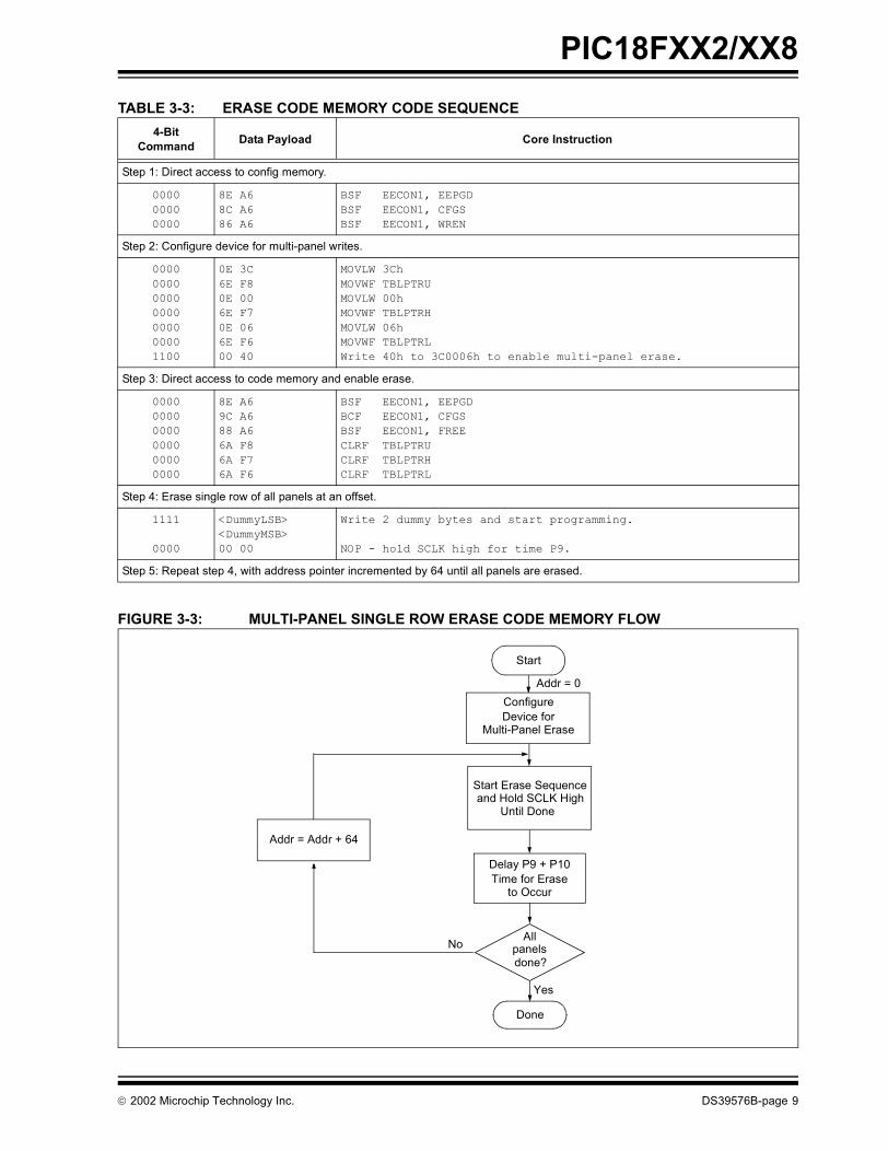
3.1.2 ICSP MULTI-PANEL SINGLE ROW ERASE
Irrespective of whether high or low voltage ICSP isused, it is possible to erase single row (64 bytes ofdata) in all panels at once. For example, in the case ofa 64-Kbyte device (8 panels), 512 bytes through 64bytes in each panel, can be erased simultaneously dur-ing each erase sequence. In this case, the offset of theerase within each panel is the same (see Figure 3-5).Multi-Panel Single Row Erase is enabled by appropri-ately configuring the Programming Control registerlocated at 3C0006h.
The multi-panel single row erase duration is externallytimed and is controlled by SCLK. After a “Start Pro-gramming” command is issued (4-bit command,‘1111’), a NOP is issued, where the 4th SCLK is heldhigh for the duration of the programming time, P9.
After SCLK is brought low, the programming sequenceis terminated. SCLK must be held low for the time spec-ified by parameter P10 to allow high voltage dischargeof the memory array.
The code sequence to program a PIC18FXX2/XX8device is shown in Table 3-3. The flow chart shown inFigure 3-3 depicts the logic necessary to completelyerase a PIC18FXX2/XX8 device. The timing diagramthat details the “Start Programming” command, andparameters P9 and P10 is shown in Figure 3-6.
Note: The TBLPTR register must contain thesame offset value when initiating the pro-gramming sequence as it did when thewrite buffers were loaded.
DS39576B-page 8 2002 Microchip Technology Inc.
PIC18FXX2/XX8
TABLE 3-3: ERASE CODE MEMORY CODE SEQUENCEFIGURE 3-3: MULTI-PANEL SINGLE ROW ERASE CODE MEMORY FLOW
4-Bit Command Data Payload Core Instruction
Step 1: Direct access to config memory.
000000000000
8E A68C A686 A6
BSF EECON1, EEPGDBSF EECON1, CFGSBSF EECON1, WREN
Step 2: Configure device for multi-panel writes.
0000000000000000000000001100
0E 3C6E F80E 006E F70E 066E F600 40
MOVLW 3ChMOVWF TBLPTRUMOVLW 00hMOVWF TBLPTRHMOVLW 06hMOVWF TBLPTRLWrite 40h to 3C0006h to enable multi-panel erase.
Step 3: Direct access to code memory and enable erase.
000000000000000000000000
8E A69C A688 A66A F86A F76A F6
BSF EECON1, EEPGDBCF EECON1, CFGSBSF EECON1, FREECLRF TBLPTRUCLRF TBLPTRHCLRF TBLPTRL
Step 4: Erase single row of all panels at an offset.
1111
0000
<DummyLSB><DummyMSB>00 00
Write 2 dummy bytes and start programming.
NOP - hold SCLK high for time P9.Step 5: Repeat step 4, with address pointer incremented by 64 until all panels are erased.
Done
Start
Delay P9 + P10Time for Erase
to Occur
Allpanelsdone?
No
Yes
Addr = 0ConfigureDevice for
Multi-Panel Erase
Addr = Addr + 64
Start Erase Sequenceand Hold SCLK High
Until Done
2002 Microchip Technology Inc. DS39576B-page 9

PIC18FXX2/XX8
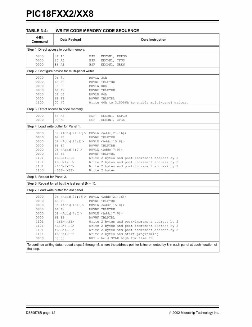
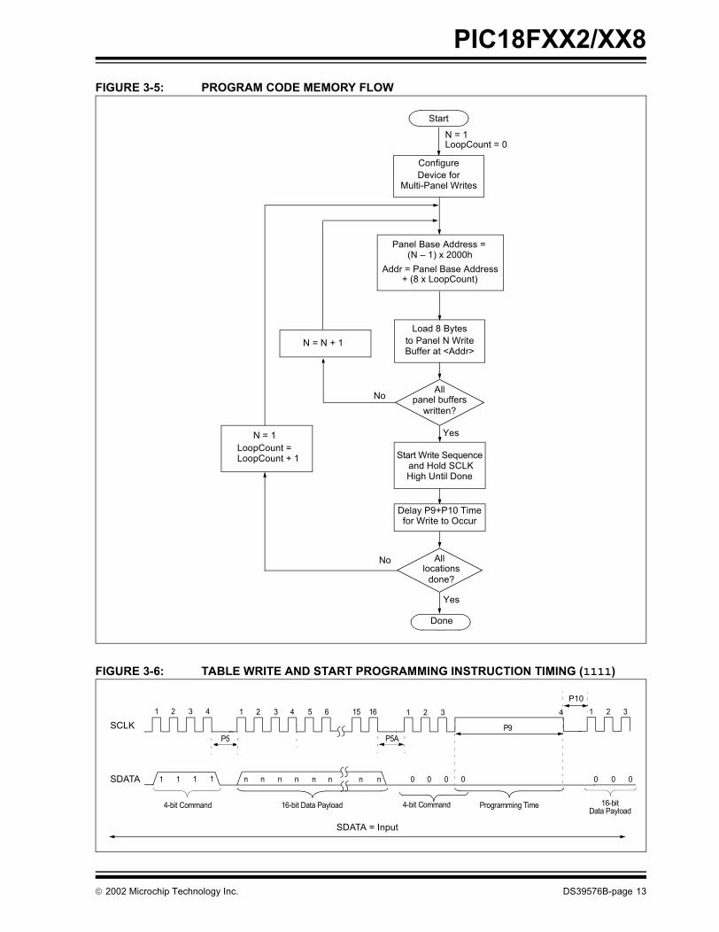
3.2 Code Memory ProgrammingProgramming code memory is accomplished by firstloading data into the appropriate write buffers and theninitiating a programming sequence. Each panel in thecode memory space (see Figure 2-2) has an 8-bytedeep write buffer that must be loaded prior to initiatinga write sequence. The actual memory write sequencetakes the contents of these buffers and programs theassociated EEPROM code memory.Typically, all of the program buffers are written in paral-lel (Multi-Panel Write mode). In other words, in the caseof a 32-Kbyte device (4 panels with an 8-byte buffer perpanel), 32 bytes will be simultaneously programmedduring each programming sequence. In this case, theoffset of the write within each panel is the same (seeFigure 3-4). Multi-Panel Write mode is enabled byappropriately configuring the programming controlregister located at 3C0006h.
The programming duration is externally timed and iscontrolled by SCLK. After a “Start Programming” com-mand is issued (4-bit command, ‘1111’), a NOP isissued, where the 4th SCLK is held high for theduration of the programming time, P9.
After SCLK is brought low, the programming sequenceis terminated. SCLK must be held low for the time spec-ified by parameter P10 to allow high voltage dischargeof the memory array.
The code sequence to program a PIC18FXX2/XX8device is shown in Figure 3-4. The flow chart shown inFigure 3-5 depicts the logic necessary to completelywrite a PIC18FXX2/XX8 device.
Note: The TBLPTR register must contain thesame offset value when initiating the pro-gramming sequence as it did when thewrite buffers were loaded.
DS39576B-page 10 2002 Microchip Technology Inc.

PIC18FXX2/XX8
FIGURE 3-4: ERASE AND WRITE BOUNDARIESTBLPTR<2:0> = 0TBLPTR<2:0> = 1TBLPTR<2:0> = 2TBLPTR<2:0> = 3TBLPTR<2:0> = 4TBLPTR<2:0> = 5TBLPTR<2:0> = 6TBLPTR<2:0> = 7
Offset = TBLPTR<12:3>
TBLPTR<21:13> = 0
Offset = TBLPTR<12:6>
Panel 1
Erase Region(64 bytes)
8-by
te W
rite
Buf
fer
TBLPTR<2:0> = 0TBLPTR<2:0> = 1TBLPTR<2:0> = 2TBLPTR<2:0> = 3TBLPTR<2:0> = 4TBLPTR<2:0> = 5TBLPTR<2:0> = 6TBLPTR<2:0> = 7
Offset = TBLPTR<12:3>
TBLPTR<21:13> = 1
Offset = TBLPTR<12:6>
Panel 2
Erase Region(64 bytes)
8-by
te W
rite
Buffe
r
TBLPTR<2:0> = 0TBLPTR<2:0> = 1TBLPTR<2:0> = 2TBLPTR<2:0> = 3TBLPTR<2:0> = 4TBLPTR<2:0> = 5TBLPTR<2:0> = 6TBLPTR<2:0> = 7
Offset = TBLPTR<12:3>
TBLPTR<21:13> = 2
Offset = TBLPTR<12:6>
Panel 3
Erase Region(64 bytes)
8-by
te W
rite
Buf
fer
TBLPTR<2:0> = 0TBLPTR<2:0> = 1TBLPTR<2:0> = 2TBLPTR<2:0> = 3TBLPTR<2:0> = 4TBLPTR<2:0> = 5TBLPTR<2:0> = 6TBLPTR<2:0> = 7
Offset = TBLPTR<12:3>
TBLPTR<21:13> = (n – 1)
Offset = TBLPTR<12:6>
Panel n
Erase Region(64 bytes)
8-by
te W
rite
Buf
fer
Note: TBLPTR = TBLPTRU:TBLPTRH:TBLPTRL.
2002 Microchip Technology Inc. DS39576B-page 11
PIC18FXX2/XX8
TABLE 3-4: WRITE CODE MEMORY CODE SEQUENCE4-Bit Command Data Payload Core Instruction
Step 1: Direct access to config memory.
000000000000
8E A68C A686 A6
BSF EECON1, EEPGDBSF EECON1, CFGSBSF EECON1, WREN
Step 2: Configure device for multi-panel writes.
0000000000000000000000001100
0E 3C6E F80E 006E F70E 066E F600 40
MOVLW 3ChMOVWF TBLPTRUMOVLW 00hMOVWF TBLPTRHMOVLW 06hMOVWF TBLPTRLWrite 40h to 3C0006h to enable multi-panel writes.
Step 3: Direct access to code memory.
00000000
8E A69C A6
BSF EECON1, EEPGDBCF EECON1, CFGS
Step 4: Load write buffer for Panel 1.
0000000000000000000000001101110111011100
0E <Addr[21:16]>6E F80E <Addr[15:8]>6E F70E <Addr[7:0]>6E F6<LSB><MSB><LSB><MSB><LSB><MSB><LSB><MSB>
MOVLW <Addr[21:16]>MOVWF TBLPTRUMOVLW <Addr[15:8]>MOVWF TBLPTRHMOVLW <Addr[7:0]>MOVWF TBLPTRLWrite 2 bytes and post-increment address by 2Write 2 bytes and post-increment address by 2Write 2 bytes and post-increment address by 2Write 2 bytes
Step 5: Repeat for Panel 2.
Step 6: Repeat for all but the last panel (N – 1).
Step 7: Load write buffer for last panel.
00000000000000000000000011011101110111110000
0E <Addr[21:16]>6E F80E <Addr[15:8]>6E F70E <Addr[7:0]>6E F6<LSB><MSB><LSB><MSB><LSB><MSB><LSB><MSB>00 00
MOVLW <Addr[21:16]>MOVWF TBLPTRUMOVLW <Addr[15:8]>MOVWF TBLPTRHMOVLW <Addr[7:0]>MOVWF TBLPTRLWrite 2 bytes and post-increment address by 2Write 2 bytes and post-increment address by 2Write 2 bytes and post-increment address by 2Write 2 bytes and start programmingNOP - hold SCLK high for time P9
To continue writing data, repeat steps 2 through 5, where the address pointer is incremented by 8 in each panel at each iteration of the loop.
DS39576B-page 12 2002 Microchip Technology Inc.
PIC18FXX2/XX8
FIGURE 3-5: PROGRAM CODE MEMORY FLOWFIGURE 3-6: TABLE WRITE AND START PROGRAMMING INSTRUCTION TIMING (1111)
Start Write Sequence
Alllocations
done?
No
Done
Start
Yes
Delay P9+P10 Timefor Write to Occur
Load 8 Bytesto Panel N WriteBuffer at <Addr>
Allpanel buffers
written?No
Yes
and Hold SCLKHigh Until Done
N = 1LoopCount = 0
ConfigureDevice for
Multi-Panel Writes
N = 1LoopCount =LoopCount + 1
N = N + 1
Panel Base Address = (N – 1) x 2000h
Addr = Panel Base Address+ (8 x LoopCount)
1 2 3 4 1 2 15 16 1 2 3 4SCLK
P5A
SDATA
SDATA = Input
n1 1 1 1
3 4 65
P9
P10
Programming Time
n n n n n n n 0 0
1 2
00 0
16-bitData Payload
0
3
0
P5
4-bit Command 16-bit Data Payload 4-bit Command
2002 Microchip Technology Inc. DS39576B-page 13

PIC18FXX2/XX8
3.2.1 SINGLE PANEL PROGRAMMINGThe programming example presented in Section 3.2utilizes multi-panel programming. This techniquegreatly decreases the total amount of time necessary tocompletely program a device and is the recommendedmethod of completely programming a device.
There may be situations, however, where it is advanta-geous to limit writes to a single panel. In such cases,the user only needs to disable the multi-panel writefeature of the device by appropriately configuring theprogramming control register located at 3C0006h.
The single panel that will be written will automaticallybe enabled, based on the value of the Table Pointer.
3.2.2 MODIFYING CODE MEMORY
All of the programming examples up to this point haveassumed that the device is blank prior to programming.In fact, if the device is not blank, the direction has beento completely erase the device via a Bulk Eraseoperation (see Section 3.1) operation.
It may be the case, however, that the user wishes tomodify only a section of an already programmeddevice. In such a situation, erasing the entire device isnot a realistic option.
The minimum amount of data that can be written to thedevice is 8 bytes. This is accomplished by placing thedevice in Single Panel Write mode (see Section 3.2.1),loading the 8-byte write buffer for the panel, and theninitiating a write sequence. In this case, however, it isassumed that the address space to be written alreadyhas data in it (i.e., it is not blank).
The minimum amount of code memory that may beerased at a given time is 64 bytes. Again, the devicemust be placed in Single Panel Write mode. TheEECON1 register must then be used to erase the64-byte target space prior to writing the data.
When using the EECON1 register to act on code mem-ory, the EEPGD bit must be set (EECON1<7> = 1) andthe CFGS bit must be cleared (EECON1<6> = 0). TheWREN bit must be set (EECON1<2> = 1) to enablewrites of any sort (e.g., erases), and this must be doneprior to initiating a write sequence. The FREE bit mustbe set (EECON1<4> = 1) in order to erase the programspace being pointed to by the Table Pointer. The erasesequence is initiated by the setting the WR bit(EECON1<1> = 1). It is strongly recommended that theWREN bit be set only when absolutely necessary.
To help prevent inadvertent writes when using theEECON1 register, EECON2 is used to “enable” the WRbit. This register must be sequentially loaded with 55hand then, AAh, immediately prior to asserting the WRbit in order for the write to occur.
The erase will begin on the falling edge of the 4th SCLKafter the WR bit is set.
After the erase sequence terminates, SCLK must stillbe held low for the time specified by parameter P10 toallow high voltage discharge of the memory array.
Note: For single panel programming, the usermust still fill the 8-byte write buffer for thegiven panel.
DS39576B-page 14 2002 Microchip Technology Inc.

PIC18FXX2/XX8
TABLE 3-5: MODIFYING CODE MEMORY4-BitCommand Data Payload Core Instruction
Step 1: Direct access to config memory.
00000000
8E A68C A6
BSF EECON1, EEPGDBSF EECON1, CFGS
Step 2: Configure device for single panel writes.
0000000000000000000000001100
0E 3C6E F80E 006E F70E 066E F600 00
MOVLW 3ChMOVWF TBLPTRUMOVLW 00hMOVWF TBLPTRHMOVLW 06hMOVWF TBLPTRLWrite 00h to 3C0006h to enable single-panel writes.
Step 3: Direct access to code memory.
00000000
8E A69C A6
BSF EECON1, EEPGDBCF EECON1, CFGS
Step 4: Set the Table Pointer for the block to be erased.
000000000000000000000000
0E <Addr[21:16]>6E F80E <Addr[8:15]>6E F70E <Addr[7:0]>6E F6
MOVLW <Addr[21:16]>MOVWF TBLPTRUMOVLW <Addr[8:15]>MOVWF TBLPTRHMOVLW <Addr[7:0]>MOVWF TBLPTRL
Step 5: Enable memory writes and setup an erase.
00000000
84 A688 A6
BSF EECON1, WRENBSF EECON1, FREE
Step 6: Perform required sequence.
0000000000000000
0E 556E A70E AA6E A7
MOVLW 55hMOVWF EECON2MOVLW 0AAhMOVWF EECON2
Step 7: Initiate erase.
00000000
82 A600 00
BSF EECON1, WRNOP
Step 8: Wait for P11+P10 and then disable writes.
0000 94 A6 BCF EECON1, WRENStep 9: Load write buffer for panel. The correct panel will be selected based on the Table Pointer.
000000000000000011011101110111110000
0E <Addr[8:15]>6E F70E <Addr[7:0]>6E F6<LSB><MSB><LSB><MSB><LSB><MSB><LSB><MSB>00 00
MOVLW <Addr[8:15]>MOVWF TBLPTRHMOVLW <Addr[7:0]>MOVWF TBLPTRLWrite 2 bytes and post-increment address by 2Write 2 bytes and post-increment address by 2Write 2 bytes and post-increment address by 2Write 2 bytes and start programmingNOP - hold SCLK high for time P9
To continue writing data, repeat step 8, where the address pointer is incremented by 8 at each iteration of the loop.
2002 Microchip Technology Inc. DS39576B-page 15

PIC18FXX2/XX8
3.3 Data EEPROM Programming Data EEPROM is accessed one byte at a time via anaddress pointer, EEADR, and a data latch, EEDATA.Data EEPROM is written by loading EEADR with thedesired memory location, EEDATA with the data to bewritten, and initiating a memory write by appropriatelyconfiguring the EECON1 and EECON2 registers. Abyte write automatically erases the location and writesthe new data (erase-before-write).When using the EECON1 register to perform a dataEEPROM write, the EEPGD bit must be cleared(EECON1<7> = 0) and the CFGS bit must be cleared(EECON1<6> = 0). The WREN bit must be set(EECON1<2> = 1) to enable writes of any sort, and thismust be done prior to initiating a write sequence. Thewrite sequence is initiated by the setting the WR bit(EECON1<1> = 1). It is strongly recommended that theWREN bit be set only when absolutely necessary.
To help prevent inadvertent writes when using theEECON1 register, EECON2 is used to “enable” the WRbit. This register must be sequentially loaded with 55hand then, AAh, immediately prior to asserting the WRbit in order for the write to occur.
The write will begin on the falling edge of the 4th SCLKafter the WR bit is set.
After the programming sequence terminates, SCLKmust still be held low for the time specified byparameter P10 to allow high voltage discharge of thememory array.
FIGURE 3-7: PROGRAM DATA FLOW
FIGURE 3-8: DATA EEPROM WRITE TIMING
Start
Start Write
Set Data
Done
No
Yes
Done?
Enable Write
Unlock Sequence55h - EECON2AAh - EECON2
Sequence
Set Address
WR bitclear?
No
Yes
n
SCLK
SDATA
SDATA = Input
0 0 0 0
BSF EECON1, WR4-bit Command
1 2 3 4 1 2 15 16
P5 P5A
P101 2
n
Poll WR bit, Repeat Until Clear 16-bit DataPayload
1 2 3 4 1 2 15 16 1 2 3
P5 P5A
4 1 2 15 16
P5 P5A
0 0 0 0
MOVF EECON1, W, 04-bit Command
0 0 0 0
4-bit Command Shift Out DataMOVWF TABLAT
SCLK
SDATA
(see below)
(see Figure 4-6)
SDATA = Input SDATA = Output
Poll WR bit
DS39576B-page 16 2002 Microchip Technology Inc.

PIC18FXX2/XX8
TABLE 3-6: PROGRAMMING DATA MEMORY4-BitCommand Data Payload Core Instruction
Step 1: Direct access to data EEPROM.
00000000
9E A69C A6
BCF EECON1, EEPGDBCF EECON1, CFGS
Step 2: Set the data EEPROM address pointer.
0000000000000000
0E <Addr>6E A9OE <AddrH>6E AA
MOVLW <Addr>MOVWF EEADRMOVLW <AddrH>MOVWF EEADRH
Step 3: Load the data to be written.
00000000
0E <Data>6E A8
MOVLW <Data>MOVWF EEDATA
Step 4: Enable memory writes.
0000 84 A6 BSF EECON1, WRENStep 5: Perform required sequence.
0000000000000000
0E 556E A70E AA6E A7
MOVLW 0X55MOVWF EECON2MOVLW 0XAAMOVWF EECON2
Step 6: Initiate write.
0000 82 A6 BSF EECON1, WRStep 7: Poll WR bit, repeat until the bit is clear.
000000000010
50 A66E F5<LSB><MSB>
MOVF EECON1, W, 0MOVWF TABLATShift out data(1)
Step 8: Disable writes.
0000 94 A6 BCF EECON1, WRENRepeat steps 2 through 8 to write more data.
Note 1: See Figure 4-4 for details on Shift Out Data timing.
2002 Microchip Technology Inc. DS39576B-page 17
PIC18FXX2/XX8
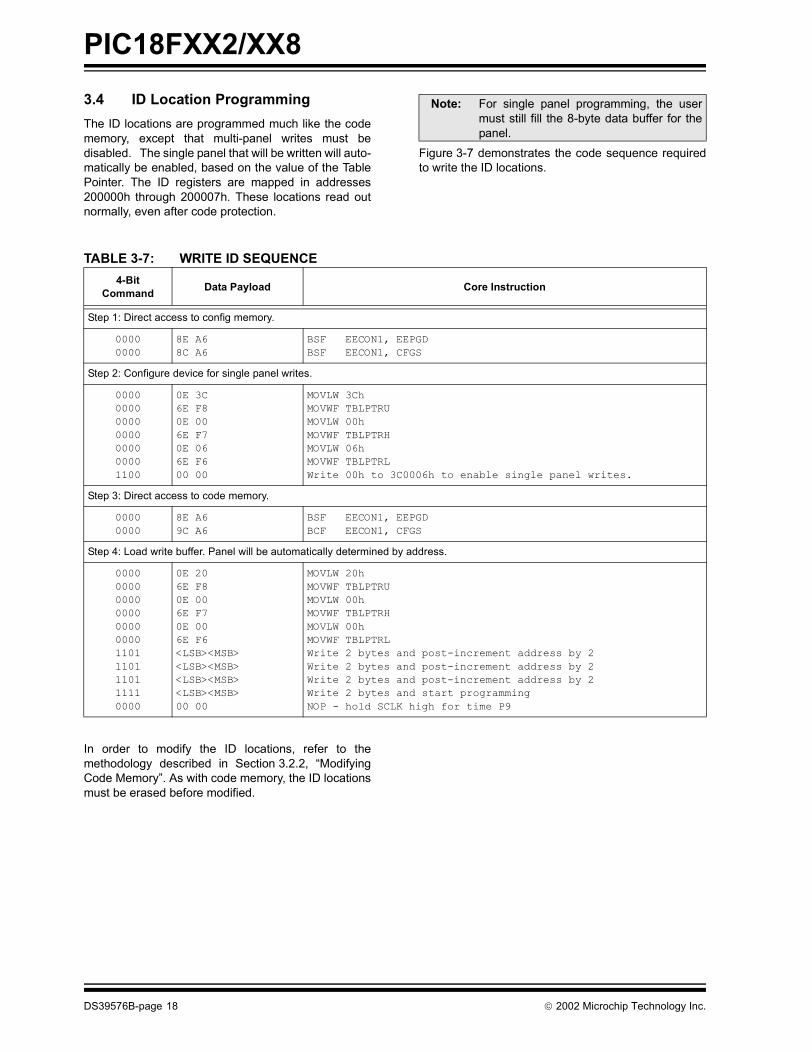
3.4 ID Location ProgrammingThe ID locations are programmed much like the codememory, except that multi-panel writes must bedisabled. The single panel that will be written will auto-matically be enabled, based on the value of the TablePointer. The ID registers are mapped in addresses200000h through 200007h. These locations read outnormally, even after code protection.Figure 3-7 demonstrates the code sequence requiredto write the ID locations.
TABLE 3-7: WRITE ID SEQUENCE
In order to modify the ID locations, refer to themethodology described in Section 3.2.2, “ModifyingCode Memory”. As with code memory, the ID locationsmust be erased before modified.
Note: For single panel programming, the usermust still fill the 8-byte data buffer for thepanel.
4-BitCommand Data Payload Core Instruction
Step 1: Direct access to config memory.
00000000
8E A68C A6
BSF EECON1, EEPGDBSF EECON1, CFGS
Step 2: Configure device for single panel writes.
0000000000000000000000001100
0E 3C6E F80E 006E F70E 066E F600 00
MOVLW 3ChMOVWF TBLPTRUMOVLW 00hMOVWF TBLPTRHMOVLW 06hMOVWF TBLPTRLWrite 00h to 3C0006h to enable single panel writes.
Step 3: Direct access to code memory.
00000000
8E A69C A6
BSF EECON1, EEPGDBCF EECON1, CFGS
Step 4: Load write buffer. Panel will be automatically determined by address.
00000000000000000000000011011101110111110000
0E 206E F80E 006E F70E 006E F6<LSB><MSB><LSB><MSB><LSB><MSB><LSB><MSB>00 00
MOVLW 20hMOVWF TBLPTRUMOVLW 00hMOVWF TBLPTRHMOVLW 00hMOVWF TBLPTRLWrite 2 bytes and post-increment address by 2Write 2 bytes and post-increment address by 2Write 2 bytes and post-increment address by 2Write 2 bytes and start programmingNOP - hold SCLK high for time P9
DS39576B-page 18 2002 Microchip Technology Inc.
PIC18FXX2/XX8
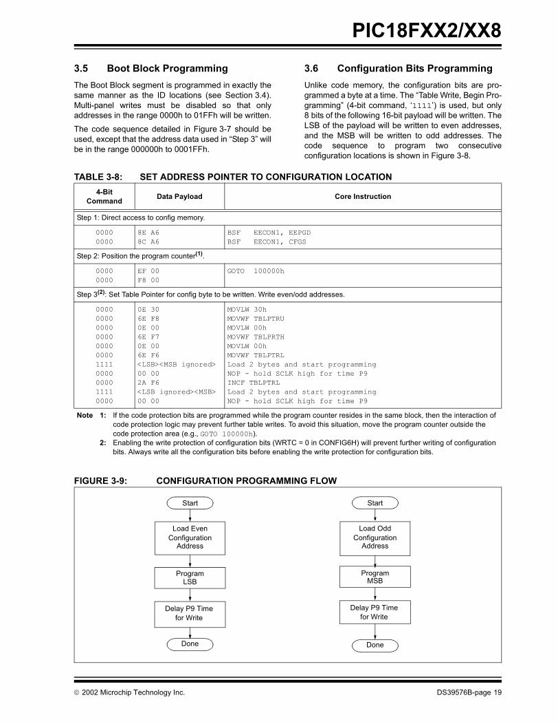
3.5 Boot Block ProgrammingThe Boot Block segment is programmed in exactly thesame manner as the ID locations (see Section 3.4).Multi-panel writes must be disabled so that onlyaddresses in the range 0000h to 01FFh will be written.The code sequence detailed in Figure 3-7 should beused, except that the address data used in “Step 3” willbe in the range 000000h to 0001FFh.
3.6 Configuration Bits ProgrammingUnlike code memory, the configuration bits are pro-grammed a byte at a time. The “Table Write, Begin Pro-gramming” (4-bit command, ‘1111’) is used, but only8 bits of the following 16-bit payload will be written. TheLSB of the payload will be written to even addresses,and the MSB will be written to odd addresses. Thecode sequence to program two consecutiveconfiguration locations is shown in Figure 3-8.
TABLE 3-8: SET ADDRESS POINTER TO CONFIGURATION LOCATION
FIGURE 3-9: CONFIGURATION PROGRAMMING FLOW
4-BitCommand Data Payload Core Instruction
Step 1: Direct access to config memory.
00000000
8E A68C A6
BSF EECON1, EEPGDBSF EECON1, CFGS
Step 2: Position the program counter(1).
00000000
EF 00F8 00
GOTO 100000h
Step 3(2): Set Table Pointer for config byte to be written. Write even/odd addresses.
00000000000000000000000011110000000011110000
0E 306E F80E 006E F70E 006E F6<LSB><MSB ignored>00 002A F6<LSB ignored><MSB>00 00
MOVLW 30hMOVWF TBLPTRUMOVLW 00hMOVWF TBLPRTHMOVLW 00hMOVWF TBLPTRLLoad 2 bytes and start programmingNOP - hold SCLK high for time P9INCF TBLPTRLLoad 2 bytes and start programmingNOP - hold SCLK high for time P9
Note 1: If the code protection bits are programmed while the program counter resides in the same block, then the interaction of code protection logic may prevent further table writes. To avoid this situation, move the program counter outside the code protection area (e.g., GOTO 100000h).
2: Enabling the write protection of configuration bits (WRTC = 0 in CONFIG6H) will prevent further writing of configuration bits. Always write all the configuration bits before enabling the write protection for configuration bits.
Load EvenConfiguration
Start
Program ProgramMSB
Done
Delay P9 Time for Write
Delay P9 Time for Write
LSB
Load OddConfiguration
Address Address
Done
Start
2002 Microchip Technology Inc. DS39576B-page 19

PIC18FXX2/XX8
4.0 READING THE DEVICE
4.1 Read Code Memory, ID Locations, and Configuration Bits
Code memory is accessed one byte at a time, via the4-bit command, ‘1001’ (Table Read, post-increment).The contents of memory pointed to by the Table Pointer(TBLPTRU:TBLPTRH:TBLPTRL) are loaded into theTable Latch and then serially output on SDATA.
The 4-bit command is shifted in LSb first. The Read isexecuted during the next 8 clocks, then shifted out onSDATA during the last 8 clocks, LSb to MSb. A delay ofP6 must be introduced after the falling edge of the 8thSCLK of the operand to allow SDATA to transition froman input to an output. During this time, SCLK must beheld low (see Table 4-1). This operation alsoincrements the Table Pointer pointer by one, pointing tothe next byte in code memory for the next read.
This technique will work to read any memory in the000000h to 3FFFFFh address space, so it also appliesto the reading of the ID and configuration registers.
TABLE 4-1: READ CODE MEMORY SEQUENCE
FIGURE 4-1: TABLE READ POST-INCREMENT INSTRUCTION TIMING (1001)
4-BitCommand Data Payload Core Instruction
Step 1: Set Table Pointer.
000000000000000000000000
0E <Addr[21:16]>6E F80E <Addr[15:8]>6E F70E <Addr[7:0]>6E F6
MOVLW Addr[21:16]MOVWF TBLPTRUMOVLW <Addr[15:8]>MOVWF TBLPTRHMOVLW <Addr[7:0]>MOVWF TBLPTRL
Step 2: Read memory into Table Latch and then shift out on SDATA, LSb to MSb.
1001 00 00 TBLRD *+
1 2 3 4SCLK
P5
SDATA
SDATA = Input
Shift Data Out
P6
SDATA = Output
5 6 7 8 1 2 3 4
P5A
9 10 11 13 15 161412
Fetch Next 4-bit Command
1 0 0 1
SDATA = Input
LSb MSb1 2 3 4 5 6
1 2 3 4
n n n n
P14
DS39576B-page 20 2002 Microchip Technology Inc.

PIC18FXX2/XX8
4.2 Verify Code Memory and IDlocationsThe verify step involves reading back the code memoryspace and comparing against the copy held in the pro-grammer’s buffer. Memory reads occur a single byte ata time, so two bytes must be read to compare againstthe word in the programmer’s buffer. Refer toSection 4.1 for implementation details of reading codememory.
The Table Pointer must be manually set to 200000h(base address of the ID locations) once the code mem-ory has been verified. The post-increment feature ofthe Table Read 4-bit command may not be used toincrement the Table Pointer beyond 1FFFFFh.
FIGURE 4-2: VERIFY CODE MEMORY FLOW
Read Low Byte
Read High Byte
Doesword = expect
data?Failure,ReportError
Allcode memory
verified?No
Yes
No
Set Pointer = 0
Start
Set Pointer = 200000h
Yes
Read Low Byte
Read High Byte
Doesword = expect
data?Failure,ReportError
AllID locations
verified?No
Yes
Done
Yes
No
2002 Microchip Technology Inc. DS39576B-page 21

PIC18FXX2/XX8
4.3 Verify Configuration BitsA configuration address may be read and output onSDATA via the 4-bit command, ‘1001’. Configurationdata is read and written in a bytewise fashion, so it isnot necessary to merge two bytes into a word prior to acompare. The result may then be immediatelycompared to the appropriate configuration data in theprogrammer’s memory for verification. Refer toSection 4.1 for implementation details of readingconfiguration data.4.4 Read Data EEPROM MemoryData EEPROM is accessed one byte at a time via anaddress pointer, EEADR, and a data latch, EEDATA.Data EEPROM is read by loading EEADR with thedesired memory location and initiating a memory readby appropriately configuring the EECON1 register. Thedata will be loaded into EEDATA, where it may be seri-ally output on SDATA via the 4-bit command, ‘0010’(shift out data holding register). A delay of P6 must beintroduced after the falling edge of the 8th SCLK of theoperand to allow SDATA to transition from an input toan output. During this time, SCLK must be held low(see Figure 4-4).
The command sequence to read a single byte of datais shown in Figure 4-2.
FIGURE 4-3: READ DATA EEPROM FLOW
TABLE 4-2: READ DATA EEPROM MEMORY
Start
SetAddress
ReadByte
Done
No
Yes
Done?
Move to TABLAT
Shift Out Data
4-BitCommand Data Payload Core Instruction
Step 1: Direct access to data EEPROM.
00000000
9E A69C A6
BCF EECON1, EEPGDBCF EECON1, CFGS
Step 2: Set the data EEPROM address pointer.
0000000000000000
0E <Addr>6E A9OE <AddrH>6E AA
MOVLW <Addr>MOVWF EEADRMOVLW <AddrH>MOVWF EEADRH
Step 3: Initiate a memory read.
0000 80 A6 BSF EECON1, RDStep 4: Load data into the serial data holding register.
000000000010
50 A86E F5<LSB><MSB>
MOVF EEDATA, W, 0MOVWF TABLATShift Out Data(1)
Note 1: The <LSB> is undefined. The <MSB> is the data.
DS39576B-page 22 2002 Microchip Technology Inc.

PIC18FXX2/XX8
FIGURE 4-4: SHIFT OUT DATA HOLDING REGISTER TIMING (0010)4.5 Verify Data EEPROMA data EEPROM address may be read via a sequenceof core instructions (4-bit command, ‘0000’) and thenoutput on SDATA via the 4-bit command, ‘0010’ (shiftout data holding register). The result may then beimmediately compared to the appropriate data in theprogrammer’s memory for verification. Refer toSection 4.4 for implementation details of reading dataEEPROM.
4.6 Blank CheckThe term “Blank Check” means to verify that the devicehas no programmed memory cells. All memories mustbe verified: code memory, data EEPROM, ID locations,and configuration bits. The Device ID registers(3FFFFEh:3FFFFFh) should be ignored.
A “blank” or “erased” memory cell will read as a ‘1’. So,“Blank Checking” a device merely means to verify thatall bytes read as FFh, except the configuration bits.Unused (reserved) configuration bits will read ‘0’ (pro-grammed). Refer to Table 5-2 for blank configurationexpect data for the various PIC18FXX2/XX8 devices.
If it is determined that the device is not blank, then thedevice should be Bulk Erased (see Section 3.1) beforeany attempt to program is made.
Given that “Blank Checking” is merely code and dataEEPROM verification with FFh expect data, refer toSection 4.4 and Section 4.2 for implementation details.
FIGURE 4-5: BLANK CHECK FLOW
1 2 3 4SCLK
P5
SDATA
SDATA = Input
Shift Data Out
P6
SDATA = Output
5 6 7 8 1 2 3 4
P5A
9 10 11 13 15 161412
Fetch Next 4-bit Command
0 1 0 0
SDATA = Input
LSb MSb1 2 3 4 5 6
1 2 3 4
n n n n
P14
Yes
No
Start
Blank Check Device
Isdeviceblank?
Continue
Abort
2002 Microchip Technology Inc. DS39576B-page 23

PIC18FXX2/XX8
5.0 CONFIGURATION WORDThe PIC18FXX2/XX8 has several configuration words.These bits can be set or cleared to select variousdevice configurations. All other memory areas shouldbe programmed and verified prior to setting configura-tion words. These bits may be read out normally, evenafter read or code protected.
5.1 ID Locations A user may store identification information (ID) in eightID locations mapped in 200000h:200007h. It isrecommended that the most significant nibble of eachID be 0Fh. In doing so, if the user code inadvertentlytries to execute from the ID space, the ID data willexecute as NOP.
5.2 Device ID Word The device ID word for the PIC18FXX2/XX8 is locatedat 3FFFFEh:3FFFFFh. These bits may be used by theprogrammer to identify what device type is being pro-grammed and read out normally, even after code orread protected.
5.3 Low Voltage Programming (LVP) Bit
The LVP bit in configuration register CONFIG4Lenables low voltage ICSP programming. The LVP bitdefaults to a ‘1’ from the factory.
If Low Voltage Programming mode is not used, the LVPbit can be programmed to a ‘0’ and RB5/PGM becomesa digital I/O pin. However, the LVP bit may only be pro-grammed by entering the High Voltage ICSP mode,where MCLR/VPP is raised to VIHH. Once the LVP bit isprogrammed to a ‘0’, only the High Voltage ICSP modeis available and only the High Voltage ICSP mode canbe used to program the device.
.
TABLE 5-1: DEVICE ID VALUE
Note 1: The normal ICSP mode is always avail-able, regardless of the state of the LVP bit,by applying VIHH to the MCLR/VPP pin.
2: While in Low Voltage ICSP mode, the RB5pin can no longer be used as a generalpurpose I/O. The RB5 pin should be heldlow during normal operation to protectagainst inadvertent ICSP mode entry.
DeviceDevice ID Value
DEVID2 DEVID1
PIC18F242 04h 100x xxxxPIC18F248 08h 000x xxxxPIC18F252 04h 000x xxxxPIC18F258 08h 010x xxxxPIC18F442 04h 101x xxxxPIC18F448 08h 001x xxxxPIC18F452 04h 001x xxxxPIC18F458 08h 011x xxxx
DS39576B-page 24 2002 Microchip Technology Inc.

PIC18FXX2/XX8
TABLE 5-2: PIC18FXX2/XX8 CONFIGURATION BITS AND DEVICE IDSFile Name Bit 7 Bit 6 Bit 5 Bit 4 Bit 3 Bit 2 Bit 1 Bit 0 Erased or“Blank” Value
300000h CONFIG1L — — — — — — — — 0000 0000300001h CONFIG1H — — OSCEN — — FOSC2 FOSC1 FOSC0 0010 0111300002h CONFIG2L — — — — BORV1 BORV2 BOREN PWRTE 0000 1111300003h CONFIG2H — — — — WDTPS2 WDTPS1 WDTPS0 WDTEN 0000 1111300004h CONFIG3L — — — — — — — — 0000 0000300005h CONFIG3H — — — — — — — CCP2MX* 0000 0001300006h CONFIG4L BKBUG — — — — LVP — STVREN 1000 0101300007h CONFIG4H — — — — — — — — 0000 0000300008h CONFIG5L — — — — CP3 CP2 CP1 CP0 0000 1111300009h CONFIG5H CPD CPB — — — — — — 1100 000030000Ah CONFIG6L — — — — WRT3 WRT2 WRT1 WRT0 0000 111130000Bh CONFIG6H WRTD WRTB WRTC — — — — — 1110 000030000Ch CONFIG7L — — — — EBTR3 EBTR2 EBTR1 EBTR0 0000 111130000Dh CONFIG7H — EBTRB — — — — — — 0100 00003FFFFEh DEVID1 DEV2 DEV1 DEV0 REV4 REV3 REV2 REV1 REV0 Table 5-13FFFFFh DEVID2 DEV10 DEV9 DEV8 DEV7 DEV6 DEV5 DEV4 DEV3 Table 5-1* This bit only applies to the PIC18FXX2 devices.
2002 Microchip Technology Inc. DS39576B-page 25

PIC18FXX2/XX8
TABLE 5-3: PIC18FXX2/XX8 BIT DESCRIPTION
Bit Name Configuration Words Description
OSCEN CONFIG1H Low Power System Clock Option (Timer1) Enable bit1 = Disabled0 = Timer1 oscillator system clock option enabled
FOSC2:FOSC0 CONFIG1H Oscillator Selection bits111 = RC oscillator w/ OSC2 configured as RA6110 = HS oscillator w/ PLL enabled101 = EC oscillator w/ OSC2 configured as RA6100 = RC oscillator w/ OSC2 configured as “divide by 4 clock output”011 = RC oscillator010 = HS oscillator001 = XT oscillator000 = LP oscillator
BORV1:BORV0 CONFIG2L Brown-out Reset Voltage bits11 = VBOR set to 2.0V10 = VBOR set to 2.7V01 = VBOR set to 4.2V00 = VBOR set to 4.5V
BOREN CONFIG2L Brown-out Reset Enable bit1 = Brown-out Reset enabled0 = Brown-out Reset disabled
PWRTEN CONFIG2L Power-up Timer Enable bit1 = PWRT disabled0 = PWRT enabled
WDTPS2:WDTPS0 CONFIG2H Watchdog Timer Postscaler Select bits111 = 1:128110 = 1:64101 = 1:32100 = 1:16011 = 1:8010 = 1:4001 = 1:2000 = 1:1
WDTEN CONFIG2H Watchdog Timer Enable bit1 = WDT enabled0 = WDT disabled (control is placed on SWDTEN bit)
CCP2MX(1) CONFIG3H CCP2 MUX bit1 = CCP2 input/output is multiplexed with RC10 = CCP2 input/output is multiplexed with RB3
BKBUG CONFIG4L Background Debugger Enable bit1 = Background debugger disabled0 = Background debugger enabled
LVP CONFIG4L Low Voltage Programming Enable bit1 = Low voltage programming enabled0 = Low voltage programming disabled
STVREN CONFIG4L Stack Overflow/Underflow Reset Enable bit1 = Stack overflow/underflow will cause RESET0 = Stack overflow/underflow will not cause RESET
Note 1: This bit only applies to the PIC18FXX2 devices.2: These bits only apply to the PIC18FX52/X58 devices.
DS39576B-page 26 2002 Microchip Technology Inc.

PIC18FXX2/XX8
CP0 CONFIG5L Code Protection bits (code memory area 0200h - 1FFFh)1 = Code memory not code protected0 = Code memory code protected
CP1 CONFIG5L Code Protection bits (code memory area 2000h - 3FFFh)1 = Code memory not code protected0 = Code memory code protected
CP2(2) CONFIG5L Code Protection bits (code memory area 4000h - 5FFFh)1 = Code memory not code protected0 = Code memory code protected
CP3(2) CONFIG5L Code Protection bits (code memory area 6000h - 7FFFh)1 = Code memory not code protected0 = Code memory code protected
CPD CONFIG5H Code Protection bits (data EEPROM)1 = Data EEPROM not code protected0 = Data EEPROM code protected
CPB CONFIG5H Code Protection bits (boot block, memory area 0000h - 01FFh)1 = Boot block not code protected0 = Boot block code protected
WRT0 CONFIG6L Table Write Protection bit (code memory area 0200h - 1FFFh)1 = Code memory not write protected0 = Code memory write protected
WRT1 CONFIG6L Table Write Protection bit (code memory area 2000h - 3FFFh)1 = Code memory not write protected0 = Code memory write protected
WRT2(2) CONFIG6L Table Write Protection bit (code memory area 4000h - 5FFFh)1 = Code memory not write protected0 = Code memory write protected
WRT3(2) CONFIG6L Table Write Protection bit (code memory area 6000h - 7FFFh)1 = Code memory not write protected0 = Code memory write protected
WRTD CONFIG6H Table Write Protection bit (data EEPROM)1 = Data EEPROM not write protected0 = Data EEPROM write protected
WRTB CONFIG6H Table Write Protection bit (boot block, memory area 0000h - 01FFh)1 = Boot block not write protected0 = Boot block write protected
WRTC CONFIG6H Table Write Protection bit (Configuration registers)1 = Configuration registers not write protected0 = Configuration registers write protected
TABLE 5-3: PIC18FXX2/XX8 BIT DESCRIPTION (CONTINUED)
Bit Name Configuration Words Description
Note 1: This bit only applies to the PIC18FXX2 devices.2: These bits only apply to the PIC18FX52/X58 devices.
2002 Microchip Technology Inc. DS39576B-page 27

PIC18FXX2/XX8
5.4 Embedding Configuration Word Information in the HEX File
To allow portability of code, a PIC18FXX2/XX8 pro-grammer is required to read the configuration wordlocations from the HEX file. If configuration word infor-mation is not present in the HEX file, then a simplewarning message should be issued. Similarly, whilesaving a HEX file, all configuration word informationmust be included. An option to not include the configu-ration word information may be provided. Whenembedding configuration word information in the HEXfile, it should start at address 300000h.
Microchip Technology Inc. feels strongly that thisfeature is important for the benefit of the end customer.
5.5 Checksum ComputationThe checksum is calculated by summing the following:
• The contents of all code memory locations• The configuration word, appropriately masked• ID locations
The Least Significant 16-bits of this sum are thechecksum.
Table 5-4 describes how to calculate the checksum foreach device.
EBTR0 CONFIG7L Table Read Protection bit (code memory area 0200h - 01FFFh)1 = Code memory not protected from table reads executed in other blocks0 = Code memory protected from table reads executed in other blocks
EBTR1 CONFIG7L Table Read Protection bit (code memory area 2000h - 3FFFh)1 = Code memory not protected from table reads executed in other blocks0 = Code memory protected from table reads executed in other blocks
EBTR2(2) CONFIG7L Table Read Protection bit (code memory area 4000h - 5FFFh)1 = Code memory not protected from table reads executed in other blocks0 = Code memory protected from table reads executed in other blocks
EBTR3(2) CONFIG7L Table Read Protection bit (code memory area 6000h - 7FFFh)1 = Code memory not protected from table reads executed in other blocks0 = Code memory protected from table reads executed in other blocks
EBTRB CONFIG7H Table Read Protection bit (boot block, memory area 0000h - 01FFh)1 = Boot block not protected from table reads executed in other blocks0 = Boot block protected from table reads executed in other blocks
DEV10:DEV3 DEVID2 Device ID bitsThese bits are used with the DEV2:DEV0 bits in the DEVID1 register to identify part number.
DEV2:DEV0 DEVID1 Device ID bitsThese bits are used with the DEV10:DEV3 bits in the DEVID2 register to identify part number.
REV4:REV0 DEVID1 These bits are used to indicate the revision of the device.
TABLE 5-3: PIC18FXX2/XX8 BIT DESCRIPTION (CONTINUED)
Bit Name Configuration Words Description
Note 1: This bit only applies to the PIC18FXX2 devices.2: These bits only apply to the PIC18FX52/X58 devices.
Note 1: The checksum calculation differs depend-ing on the code protect setting. Since thecode memory locations read out differentlydepending on the code protect setting, thetable describes how to manipulate theactual code memory values to simulate thevalues that would be read from a protecteddevice. When calculating a checksum byreading a device, the entire code memorycan simply be read and summed. The con-figuration word and ID locations canalways be read.
DS39576B-page 28 2002 Microchip Technology Inc.

PIC18FXX2/XX8
TABLE 5-4: CHECKSUM COMPUTATION
Device CodeProtect Checksum Blank
Value
0xAA at 0and MaxAddress
PIC18F242 None SUM(0000:01FF)+SUM(0200:1FFF)+SUM(2000:3FFF)+(CFGW1L & 0000)+(CFGW1H & 0027)+(CFGW2L + 000F)&(CFGW2H &000F)+(CFGW3L & 0000)+(CFGW3H & 0001)+(CFGW4L &0085)+(CFGW4H & 0000)+(CFGW5L & 0003)+(CFGW5H &00C0)+(CFGW6L & 0003)+(CFGW6H & 00E0)+(CFGW7L &0003)+(CFGW7H & 0040)
C2B4 C20A
Boot Block SUM(0200:1FFF)+SUM(2000:3FFF)+(CFGW1L & 0000)+(CFGW1H & 0027)+(CFGW2L & 000F)+(CFGW2H & 000F)+(CFGW3L & 0000)+(CFGW3H & 0001)+(CFGW4L & 0085)+(CFGW4H & 0000)+(CFGW5L & 0003)+(CFGW5H & 00C0)+(CFGW6L & 0003)+(CFGW6H & 00E0)+(CFGW7L & 0003)+(CFGW7H & 0040)+SUM(IDs)
C491 C437
Boot/Panel1/Panel2 (CFGW1L & 0000)+(CFGW1H & 0027)+(CFGW2L & 000F)+(CFGW2H & 000F)+(CFGW3L & 0000)+(CFGW3H & 0001)+(CFGW4L & 0085)+(CFGW4H & 0000)+(CFGW5L & 0003)+(CFGW5H & 00C0)+(CFGW6L & 0003)+(CFGW6H & 00E0)+(CFGW7L & 0003)+(CFGW7H & 0040)+SUM(IDs)
028E 289
All (CFGW1L & 0000)+(CFGW1H & 0027)+(CFGW2L & 000F)+(CFGW2H & 000F)+(CFGW3L & 0000)+(CFGW3H & 0001)+(CFGW4L & 0085)+(CFGW4H & 0000)+(CFGW5L & 0003)+(CFGW5H & 00C0)+(CFGW6L & 0003)+(CFGW6H & 00E0)+(CFGW7L & 0003)+(CFGW7H & 0040)+SUM(IDs)
028E 289
PIC18F248 None SUM(0000:01FF)+SUM(0200:1FFF)+SUM(2000:3FFF)+(CFGW1L &0000)+(CFGW1H & 0027)+(CFGW2L & 000F)+(CFGW2H &000F)+(CFGW3L & 0000)+(CFGW3H & 0000)+(CFGW4L &0085)+(CFGW4H & 0000)+(CFGW5L & 0003)+(CFGW5H &00C0)+(CFGW6L & 0003)+(CFGW6H & 00E0)+(CFGW7L &0003)+(CFGW7H & 0040)
C2B3 C209
Boot Block SUM(0200:1FFF)+SUM(2000:3FFF)+(CFGW1L & 0000)+(CFGW1H & 0027)+(CFGW2L & 000F)+(CFGW2H & 000F)+(CFGW3L & 0000)+(CFGW3H & 0000)+(CFGW4L & 0085)+(CFGW4H & 0000)+(CFGW5L & 0003)+(CFGW5H & 00C0)+(CFGW6L & 0003)+(CFGW6H & 00E0)+(CFGW7L & 0003)+(CFGW7H & 0040)+SUM(IDs)
C48F C435
Boot/Panel1/Panel2 (CFGW1L & 0000)+(CFGW1H & 0027)+(CFGW2L & 000F)+(CFGW2H & 000F)+(CFGW3L & 0000)+(CFGW3H & 0000)+(CFGW4L & 0085)+(CFGW4H & 0000)+(CFGW5L & 0003)+(CFGW5H & 00C0)+(CFGW6L & 0003)+(CFGW6H & 00E0)+(CFGW7L & 0003)+(CFGW7H & 0040)+SUM(IDs)
028C 287
All (CFGW1L & 0000)+(CFGW1H & 0027)+(CFGW2L & 000F)+(CFGW2H & 000F)+(CFGW3L & 0000)+(CFGW3H & 0000)+(CFGW4L & 0085)+(CFGW4H & 0000)+(CFGW5L & 0003)+(CFGW5H & 00C0)+(CFGW6L & 0003)+(CFGW6H & 00E0)+(CFGW7L & 0003)+(CFGW7H & 0040)+SUM(IDs)
028C 287
Legend: Item DescriptionCFGW = Configuration Word SUM[a:b] = Sum of locations a to b inclusive SUM_ID = Bytewise sum of lower four bits of all customer ID locations + = Addition & = Bitwise AND
2002 Microchip Technology Inc. DS39576B-page 29

PIC18FXX2/XX8
PIC18F252 None SUM(0000:01FF)+SUM(0200:1FFF)+SUM(2000:3FFF)+SUM(4000:5FFF)+SUM(6000:7FFF)+(CFGW1L & 0000)+(CFGW1H & 0027)+(CFGW2L + 000F)+(CFGW2H & 000F)+(CFGW3L & 0000)+(CFGW3H & 0001)+(CFGW4L & 0085)+(CFGW4H & 0000)+(CFGW5L & 000F)+(CFGW5H & 00C0)+(CFGW6L & 000F)+(CFGW6H & 00E0)+(CFGW7L & 000F)+(CFGW7H & 0040)
82D8 822E
Boot Block SUM(0200:1FFF)+SUM(2000:3FFF)+SUM(4000:5FFF)+SUM(6000:7FFF)+(CFGW1L & 0000)+(CFGW1H & 0027)+(CFGW2L + 000F)+(CFGW2H & 000F)+(CFGW3L & 0000)+(CFGW3H & 0001)+(CFGW4L & 0085)+(CFGW4H & 0000)+(CFGW5L & 000F)+(CFGW5H & 00C0)+(CFGW6L & 000F)+(CFGW6H & 00E0)+(CFGW7L & 000F)+(CFGW7H & 0040)+SUM(IDs)
84B7 845D
Boot/Panel1/Panel2 SUM(4000:5FFF)+SUM(6000:7FFF)+(CFGW1L & 0000)+(CFGW1H & 0027)+(CFGW2L + 000F)+(CFGW2H & 000F)+(CFGW3L & 0000)+(CFGW3H & 0001)+(CFGW4L & 0085)+(CFGW4H & 0000)+(CFGW5L & 000F)+(CFGW5H & 00C0)+(CFGW6L & 000F)+(CFGW6H & 00E0)+(CFGW7L & 000F)+(CFGW7H & 0040)+SUM(IDs)
C2B4 C25A
All (CFGW1L & 0000)+(CFGW1H & 0027)+(CFGW2L + 000F)+(CFGW2H & 000F)+(CFGW3L & 0000)+(CFGW3H & 0001)+(CFGW4L & 0085)+(CFGW4H & 0000)+(CFGW5L & 000F)+(CFGW5H & 00C0)+(CFGW6L & 000F)+(CFGW6H & 00E0)+(CFGW7L & 000F)+(CFGW7H & 0040)+SUM(IDs)
02A8 02A3
PIC18F258 None SUM(0000:01FF)+SUM(0200:1FFF)+SUM(2000:3FFF)+SUM(4000:5FFF)+SUM(6000:7FFF)+(CFGW1L & 0000)+(CFGW1H & 0027)+(CFGW2L + 000F)+(CFGW2H & 000F)+(CFGW3L & 0000)+(CFGW3H & 0000)+(CFGW4L & 0085)+(CFGW4H & 0000)+(CFGW5L & 000F)+(CFGW5H & 00C0)+(CFGW6L & 000F)+(CFGW6H & 00E0)+(CFGW7L & 000F)+(CFGW7H & 0040)
82D7 822D
Boot Block SUM(0200:1FFF)+SUM(2000:3FFF)+SUM(4000:5FFF)+SUM(6000:7FFF)+(CFGW1L & 0000)+(CFGW1H & 0027)+(CFGW2L + 000F)+(CFGW2H & 000F)+(CFGW3L & 0000)+(CFGW3H & 0000)+(CFGW4L & 0085)+(CFGW4H & 0000)+(CFGW5L & 000F)+(CFGW5H & 00C0)+(CFGW6L & 000F)+(CFGW6H & 00E0)+(CFGW7L & 000F)+(CFGW7H & 0040)+SUM(IDs)
84B5 845B
Boot/Panel1/Panel2 SUM(4000:5FFF)+SUM(6000:7FFF)+(CFGW1L & 0000)+(CFGW1H & 0027)+(CFGW2L + 000F)+(CFGW2H & 000F)+(CFGW3L & 0000)+(CFGW3H & 0000)+(CFGW4L & 0085)+(CFGW4H & 0000)+(CFGW5L & 000F)+(CFGW5H & 00C0)+(CFGW6L & 000F)+(CFGW6H & 00E0)+(CFGW7L & 000F)+(CFGW7H & 0040)+SUM(IDs)
C2B2 C258
All (CFGW1L & 0000)+(CFGW1H & 0027)+(CFGW2L + 000F)+(CFGW2H & 000F)+(CFGW3L & 0000)+(CFGW3H & 0000)+(CFGW4L & 0085)+(CFGW4H & 0000)+(CFGW5L & 000F)+(CFGW5H & 00C0)+(CFGW6L & 000F)+(CFGW6H & 00E0)+(CFGW7L & 000F)+(CFGW7H & 0040)+SUM(IDs)
02A6 02A1
TABLE 5-4: CHECKSUM COMPUTATION (CONTINUED)
Device CodeProtect Checksum Blank
Value
0xAA at 0and MaxAddress
Legend: Item DescriptionCFGW = Configuration Word SUM[a:b] = Sum of locations a to b inclusive SUM_ID = Bytewise sum of lower four bits of all customer ID locations + = Addition & = Bitwise AND
DS39576B-page 30 2002 Microchip Technology Inc.

PIC18FXX2/XX8
PIC18F442 None SUM(0000:01FF)+SUM(0200:1FFF)+SUM(2000:3FFF)+(CFGW1L & 0000)+(CFGW1H & 0027)+(CFGW2L + 000F)+(CFGW2H & 000F)+(CFGW3L & 0000)+(CFGW3H & 0001)+(CFGW4L & 0085)+(CFGW4H & 0000)+(CFGW5L & 0003)+(CFGW5H & 00C0)+(CFGW6L & 0003)+(CFGW6H & 00E0)+(CFGW7L & 0003)+(CFGW7H & 0040)
C3B4 C20A
Boot Block SUM(0200:1FFF)+SUM(2000:3FFF)+(CFGW1L & 0000)+(CFGW1H & 0027)+(CFGW2L + 000F)+(CFGW2H & 000F)+(CFGW3L & 0000)+(CFGW3H & 0001)+(CFGW4L & 0085)+(CFGW4H & 0000)+(CFGW5L & 0003)+(CFGW5H & 00C0)+(CFGW6L & 0003)+(CFGW6H & 00E0)+(CFGW7L & 0003)+(CFGW7H & 0040)+SUM(IDs)
C491 C437
Boot/Panel1/Panel2 (CFGW1L & 0000)+(CFGW1H & 0027)+(CFGW2L + 000F)+(CFGW2H & 000F)+(CFGW3L & 0000)+(CFGW3H & 0001)+(CFGW4L & 0085)+(CFGW4H & 0000)+(CFGW5L & 0003)+(CFGW5H & 00C0)+(CFGW6L & 0003)+(CFGW6H & 00E0)+(CFGW7L & 0003)+(CFGW7H & 0040)+SUM(IDs)
028E 289
All (CFGW1L & 0000)+(CFGW1H & 0027)+(CFGW2L + 000F)+(CFGW2H & 000F)+(CFGW3L & 0000)+(CFGW3H & 0001)+(CFGW4L & 0085)+(CFGW4H & 0000)+(CFGW5L & 0003)+(CFGW5H & 00C0)+(CFGW6L & 0003)+(CFGW6H & 00E0)+(CFGW7L & 0003)+(CFGW7H & 0040)+SUM(IDs)
028E 289
PIC18F448 None SUM(0000:01FF)+SUM(0200:1FFF)+SUM(2000:3FFF)+(CFGW1L &0000)+(CFGW1H & 0027)+(CFGW2L + 000F)+(CFGW2H &000F)+(CFGW3L & 0000)+(CFGW3H & 0000)+(CFGW4L &0085)+(CFGW4H & 0000)+(CFGW5L & 0003)+(CFGW5H &00C0)+(CFGW6L & 0003)+(CFGW6H & 00E0)+(CFGW7L &0003)+(CFGW7H & 0040)
C2B3 C209
Boot Block SUM(0200:1FFF)+SUM(2000:3FFF)+(CFGW1L & 0000)+(CFGW1H & 0027)+(CFGW2L + 000F)+(CFGW2H & 000F)+(CFGW3L & 0000)+(CFGW3H & 0000)+(CFGW4L & 0085)+(CFGW4H & 0000)+(CFGW5L & 0003)+(CFGW5H & 00C0)+(CFGW6L & 0003)+(CFGW6H & 00E0)+(CFGW7L & 0003)+(CFGW7H & 0040)+SUM(IDs)
C48F C435
Boot/Panel1/Panel2 (CFGW1L & 0000)+(CFGW1H & 0027)+(CFGW2L + 000F)+(CFGW2H & 000F)+(CFGW3L & 0000)+(CFGW3H & 0000)+(CFGW4L & 0085)+(CFGW4H & 0000)+(CFGW5L & 0003)+(CFGW5H & 00C0)+(CFGW6L & 0003)+(CFGW6H & 00E0)+(CFGW7L & 0003)+(CFGW7H & 0040)+SUM(IDs)
028C 287
All (CFGW1L & 0000)+(CFGW1H & 0027)+(CFGW2L + 000F)+(CFGW2H & 000F)+(CFGW3L & 0000)+(CFGW3H & 0000)+(CFGW4L & 0085)+(CFGW4H & 0000)+(CFGW5L & 0003)+(CFGW5H & 00C0)+(CFGW6L & 0003)+(CFGW6H & 00E0)+(CFGW7L & 0003)+(CFGW7H & 0040)+SUM(IDs)
028C 287
TABLE 5-4: CHECKSUM COMPUTATION (CONTINUED)
Device CodeProtect Checksum Blank
Value
0xAA at 0and MaxAddress
Legend: Item DescriptionCFGW = Configuration Word SUM[a:b] = Sum of locations a to b inclusive SUM_ID = Bytewise sum of lower four bits of all customer ID locations + = Addition & = Bitwise AND
2002 Microchip Technology Inc. DS39576B-page 31

PIC18FXX2/XX8
PIC18F452 None SUM(0000:01FF)+SUM(0200:1FFF)+SUM(2000:3FFF)+SUM(4000:5FFF)+SUM(6000:7FFF)+(CFGW1L & 0000)+(CFGW1H & 0027)+(CFGW2L + 000F)+(CFGW2H & 000F)+(CFGW3L & 0000)+(CFGW3H & 0001)+(CFGW4L & 0085)+(CFGW4H & 0000)+(CFGW5L & 000F)+(CFGW5H & 00C0)+(CFGW6L & 000F)+(CFGW6H & 00E0)+(CFGW7L & 000F)+(CFGW7H & 0040)
82D8 822E
Boot Block SUM(0200:1FFF)+SUM(2000:3FFF)+SUM(4000:5FFF)+SUM(6000:7FFF)+(CFGW1L & 0000)+(CFGW1H & 0027)+(CFGW2L + 000F)+(CFGW2H & 000F)+(CFGW3L & 0000)+(CFGW3H & 0001)+(CFGW4L & 0085)+(CFGW4H & 0000)+(CFGW5L & 000F)+(CFGW5H & 00C0)+(CFGW6L & 000F)+(CFGW6H & 00E0)+(CFGW7L & 000F)+(CFGW7H & 0040)+SUM(IDs)
84B7 845D
Boot/Panel1/Panel2 SUM(4000:5FFF)+SUM(6000:7FFF)+(CFGW1L & 0000)+(CFGW1H & 0027)+(CFGW2L + 000F)+(CFGW2H & 000F)+(CFGW3L & 0000)+(CFGW3H & 0001)+(CFGW4L & 0085)+(CFGW4H & 0000)+(CFGW5L & 000F)+(CFGW5H & 00C0)+(CFGW6L & 000F)+(CFGW6H & 00E0)+(CFGW7L & 000F)+(CFGW7H & 0040)+SUM(IDs)
C2B4 C25A
All (CFGW1L & 0000)+(CFGW1H & 0027)+(CFGW2L + 000F)+(CFGW2H & 000F)+(CFGW3L & 0000)+(CFGW3H & 0001)+(CFGW4L & 0085)+(CFGW4H & 0000)+(CFGW5L & 000F)+(CFGW5H & 00C0)+(CFGW6L & 000F)+(CFGW6H & 00E0)+(CFGW7L & 000F)+(CFGW7H & 0040)+SUM(IDs)
02A8 02A3
PIC18F458 None SUM(0000:01FF)+SUM(0200:1FFF)+SUM(2000:3FFF)+SUM(4000:5FFF)+SUM(6000:7FFF)+(CFGW1L & 0000)+(CFGW1H & 0027)+(CFGW2L + 000F)+(CFGW2H & 000F)+(CFGW3L & 0000)+(CFGW3H & 0000)+(CFGW4L & 0085)+(CFGW4H & 0000)+(CFGW5L & 000F)+(CFGW5H & 00C0)+(CFGW6L & 000F)+(CFGW6H & 00E0)+(CFGW7L & 000F)+(CFGW7H & 0040)
82D7 822D
Boot Block SUM(0200:1FFF)+SUM(2000:3FFF)+SUM(4000:5FFF)+SUM(6000:7FFF)+(CFGW1L & 0000)+(CFGW1H & 0027)+(CFGW2L + 000F)+(CFGW2H & 000F)+(CFGW3L & 0000)+(CFGW3H & 0000)+(CFGW4L & 0085)+(CFGW4H & 0000)+(CFGW5L & 000F)+(CFGW5H & 00C0)+(CFGW6L & 000F)+(CFGW6H & 00E0)+(CFGW7L & 000F)+(CFGW7H & 0040)+SUM(IDs)
84B5 845B
Boot/Panel1/Panel2 SUM(4000:5FFF)+SUM(6000:7FFF)+(CFGW1L & 0000)+(CFGW1H & 0027)+(CFGW2L + 000F)+(CFGW2H & 000F)+(CFGW3L & 0000)+(CFGW3H & 0000)+(CFGW4L & 0085)+(CFGW4H & 0000)+(CFGW5L & 000F)+(CFGW5H & 00C0)+(CFGW6L & 000F)+(CFGW6H & 00E0)+(CFGW7L & 000F)+(CFGW7H & 0040)+SUM(IDs)
C2B2 C258
All (CFGW1L & 0000)+(CFGW1H & 0027)+(CFGW2L + 000F)+(CFGW2H & 000F)+(CFGW3L & 0000)+(CFGW3H & 0000)+(CFGW4L & 0085)+(CFGW4H & 0000)+(CFGW5L & 000F)+(CFGW5H & 00C0)+(CFGW6L & 000F)+(CFGW6H & 00E0)+(CFGW7L & 000F)+(CFGW7H & 0040)+SUM(IDs)
02A6 02A1
TABLE 5-4: CHECKSUM COMPUTATION (CONTINUED)
Device CodeProtect Checksum Blank
Value
0xAA at 0and MaxAddress
Legend: Item DescriptionCFGW = Configuration Word SUM[a:b] = Sum of locations a to b inclusive SUM_ID = Bytewise sum of lower four bits of all customer ID locations + = Addition & = Bitwise AND
DS39576B-page 32 2002 Microchip Technology Inc.

PIC18FXX2/XX8
5.6 Embedding Data EEPROMInformation In the HEX FileTo allow portability of code, a PIC18FXX2/XX8programmer is required to read the data EEPROMinformation from the HEX file. If data EEPROM infor-mation is not present, a simple warning messageshould be issued. Similarly, when saving a HEX file, alldata EEPROM information must be included. An optionto not include the data EEPROM information may beprovided. When embedding data EEPROM informationin the HEX file, it should start at address F00000h.
Microchip Technology Inc. believes that this feature isimportant for the benefit of the end customer.
2002 Microchip Technology Inc. DS39576B-page 33

PIC18FXX2/XX8
6.0 AC/DC CHARACTERISTICS TIMING REQUIREMENTS FOR PROGRAM/VERIFY TEST MODE
Standard Operating ConditionsOperating Temperature: 10°C to 50°C unless otherwise indicated
Param No. Sym Characteristic Min Max Units Conditions
D110 VIHH High Voltage Programming Voltage on MCLR/VPP
9.00 13.25 V
D110A VIHL Low Voltage Programming Voltage on MCLR/VPP
2.00 5.50 V
D111 VDD Supply Voltage during programming 2.00 5.50 V Normal programming
4.50 5.50 V Bulk erase operations
D112 IPP Programming Current on MCLR/VPP — 300 µAD113 IDDP Supply Current during programming — 5 mAD031 VIL Input Low Voltage VSS 0.2 VSS VD041 VIH Input High Voltage 0.8 VDD VDD VD080 VOL Output Low Voltage — 0.6 V IOL = 8.5 mAD090 VOH Output High Voltage VDD – 0.7 — V IOH = -3.0 mAD012 CIO Capacitive loading on I/O pin (SDATA) — 50 pF To meet AC
specificationsP2 Tsclk Serial Clock (SCLK) period 100 — ns VDD = 5.0V
1 — µs VDD = 2.0VP2A TsclkL Serial Clock (SCLK) Low time 40 — ns VDD = 5.0V
400 — ns VDD = 2.0VP2B TsclkH Serial Clock (SCLK) High time 40 — ns VDD = 5.0V
400 — ns VDD = 2.0VP3 Tset1 Input Data Setup Time to serial clock ↓ 15 — nsP4 Thld1 Input Data Hold Time from SCLK ↓ 15 — nsP5 Tdly1 Delay between 4-bit command and
command operand20 — ns
P5A Tdly1a Delay between 4-bit command operand and next 4-bit command
20 — ns
P6 Tdly2 Delay between last SCLK ↓ of command byte to first SCLK ↑ of read of data word
20 — ns
P9 Tdly5 SCLK High time (minimum programming time)
1 — ms
P10 Tdly6 SCLK Low time after programming(high voltage discharge time)
5 — µs
P11 Tdly7 Delay to allow self-timed data write or bulk erase to occur
5 — ms
P12 Thld2 Input Data Hold time fromMCLR/VPP ↑
2 — µs
P13 Tset2 VDD ↑ Setup time to MCLR/VPP ↑ 100 — nsP14 Tvalid Data Out Valid from SCLK ↑ 10 — nsP15 Tset3 PGM ↑ Setup time to MCLR/VPP ↑ 2 — µs
DS39576B-page 34 2002 Microchip Technology Inc.
Note the following details of the code protection feature on Microchip devices:• Microchip products meet the specification contained in their particular Microchip Data Sheet.
• Microchip believes that its family of products is one of the most secure families of its kind on the market today, when used in the intended manner and under normal conditions.
• There are dishonest and possibly illegal methods used to breach the code protection feature. All of these methods, to our knowl-edge, require using the Microchip products in a manner outside the operating specifications contained in Microchip's Data Sheets. Most likely, the person doing so is engaged in theft of intellectual property.
• Microchip is willing to work with the customer who is concerned about the integrity of their code.
• Neither Microchip nor any other semiconductor manufacturer can guarantee the security of their code. Code protection does not mean that we are guaranteeing the product as “unbreakable.”
Code protection is constantly evolving. We at Microchip are committed to continuously improving the code protection features of ourproducts.
Information contained in this publication regarding deviceapplications and the like is intended through suggestion onlyand may be superseded by updates. It is your responsibility toensure that your application meets with your specifications.No representation or warranty is given and no liability isassumed by Microchip Technology Incorporated with respectto the accuracy or use of such information, or infringement ofpatents or other intellectual property rights arising from suchuse or otherwise. Use of Microchip’s products as critical com-ponents in life support systems is not authorized except withexpress written approval by Microchip. No licenses are con-veyed, implicitly or otherwise, under any intellectual propertyrights.
2002 Microchip Technology Inc.
Trademarks
The Microchip name and logo, the Microchip logo, KEELOQ,MPLAB, PIC, PICmicro, PICSTART and PRO MATE areregistered trademarks of Microchip Technology Incorporatedin the U.S.A. and other countries.
FilterLab, microID, MXDEV, MXLAB, PICMASTER, SEEVALand The Embedded Control Solutions Company areregistered trademarks of Microchip Technology Incorporatedin the U.S.A.
dsPIC, dsPICDEM.net, ECONOMONITOR, FanSense,FlexROM, fuzzyLAB, In-Circuit Serial Programming, ICSP,ICEPIC, microPort, Migratable Memory, MPASM, MPLIB,MPLINK, MPSIM, PICC, PICDEM, PICDEM.net, rfPIC, SelectMode and Total Endurance are trademarks of MicrochipTechnology Incorporated in the U.S.A. and other countries.
Serialized Quick Turn Programming (SQTP) is a service markof Microchip Technology Incorporated in the U.S.A.
All other trademarks mentioned herein are property of theirrespective companies.
© 2002, Microchip Technology Incorporated, Printed in theU.S.A., All Rights Reserved.
Printed on recycled paper.
DS39576B - page 35
Microchip received QS-9000 quality system certification for its worldwide headquarters, design and wafer fabrication facilities in Chandler and Tempe, Arizona in July 1999 and Mountain View, California in March 2002. The Company’s quality system processes and procedures are QS-9000 compliant for its PICmicro® 8-bit MCUs, KEELOQ® code hopping devices, Serial EEPROMs, microperipherals, non-volatile memory and analog products. In addition, Microchip’s quality system for the design and manufacture of development systems is ISO 9001 certified.

DS39576B-page 36 2002 Microchip Technology Inc.
AMERICASCorporate Office2355 West Chandler Blvd.Chandler, AZ 85224-6199Tel: 480-792-7200 Fax: 480-792-7277Technical Support: 480-792-7627Web Address: http://www.microchip.com
Rocky Mountain2355 West Chandler Blvd.Chandler, AZ 85224-6199Tel: 480-792-7966 Fax: 480-792-4338
Atlanta3780 Mansell Road, Suite 130Alpharetta, GA 30022Tel: 770-640-0034 Fax: 770-640-0307
Boston2 Lan Drive, Suite 120Westford, MA 01886Tel: 978-692-3848 Fax: 978-692-3821
Chicago333 Pierce Road, Suite 180Itasca, IL 60143Tel: 630-285-0071 Fax: 630-285-0075
Dallas4570 Westgrove Drive, Suite 160Addison, TX 75001Tel: 972-818-7423 Fax: 972-818-2924
DetroitTri-Atria Office Building 32255 Northwestern Highway, Suite 190Farmington Hills, MI 48334Tel: 248-538-2250 Fax: 248-538-2260
Kokomo2767 S. Albright Road Kokomo, Indiana 46902Tel: 765-864-8360 Fax: 765-864-8387
Los Angeles18201 Von Karman, Suite 1090Irvine, CA 92612Tel: 949-263-1888 Fax: 949-263-1338
San JoseMicrochip Technology Inc.2107 North First Street, Suite 590San Jose, CA 95131Tel: 408-436-7950 Fax: 408-436-7955
Toronto6285 Northam Drive, Suite 108Mississauga, Ontario L4V 1X5, CanadaTel: 905-673-0699 Fax: 905-673-6509
ASIA/PACIFICAustraliaMicrochip Technology Australia Pty LtdSuite 22, 41 Rawson StreetEpping 2121, NSWAustraliaTel: 61-2-9868-6733 Fax: 61-2-9868-6755China - BeijingMicrochip Technology Consulting (Shanghai)Co., Ltd., Beijing Liaison OfficeUnit 915Bei Hai Wan Tai Bldg.No. 6 Chaoyangmen Beidajie Beijing, 100027, No. ChinaTel: 86-10-85282100 Fax: 86-10-85282104China - ChengduMicrochip Technology Consulting (Shanghai)Co., Ltd., Chengdu Liaison OfficeRm. 2401-2402, 24th Floor, Ming Xing Financial TowerNo. 88 TIDU StreetChengdu 610016, ChinaTel: 86-28-86766200 Fax: 86-28-86766599China - FuzhouMicrochip Technology Consulting (Shanghai)Co., Ltd., Fuzhou Liaison OfficeUnit 28F, World Trade PlazaNo. 71 Wusi RoadFuzhou 350001, ChinaTel: 86-591-7503506 Fax: 86-591-7503521China - ShanghaiMicrochip Technology Consulting (Shanghai)Co., Ltd.Room 701, Bldg. BFar East International PlazaNo. 317 Xian Xia RoadShanghai, 200051Tel: 86-21-6275-5700 Fax: 86-21-6275-5060China - ShenzhenMicrochip Technology Consulting (Shanghai)Co., Ltd., Shenzhen Liaison OfficeRm. 15-16, 13/F, Shenzhen Kerry Centre,Renminnan LuShenzhen 518001, ChinaTel: 86-755-82350361 Fax: 86-755-82366086China - Hong Kong SARMicrochip Technology Hongkong Ltd.Unit 901-6, Tower 2, Metroplaza223 Hing Fong RoadKwai Fong, N.T., Hong KongTel: 852-2401-1200 Fax: 852-2401-3431IndiaMicrochip Technology Inc.India Liaison OfficeDivyasree Chambers1 Floor, Wing A (A3/A4)No. 11, O’Shaugnessey RoadBangalore, 560 025, IndiaTel: 91-80-2290061 Fax: 91-80-2290062
JapanMicrochip Technology Japan K.K.Benex S-1 6F3-18-20, ShinyokohamaKohoku-Ku, Yokohama-shiKanagawa, 222-0033, JapanTel: 81-45-471- 6166 Fax: 81-45-471-6122KoreaMicrochip Technology Korea168-1, Youngbo Bldg. 3 FloorSamsung-Dong, Kangnam-KuSeoul, Korea 135-882Tel: 82-2-554-7200 Fax: 82-2-558-5934SingaporeMicrochip Technology Singapore Pte Ltd.200 Middle Road#07-02 Prime CentreSingapore, 188980Tel: 65-6334-8870 Fax: 65-6334-8850TaiwanMicrochip Technology (Barbados) Inc., Taiwan Branch11F-3, No. 207Tung Hua North RoadTaipei, 105, TaiwanTel: 886-2-2717-7175 Fax: 886-2-2545-0139
EUROPEAustriaMicrochip Technology Austria GmbHDurisolstrasse 2A-4600 WelsAustriaTel: 43-7242-2244-399Fax: 43-7242-2244-393DenmarkMicrochip Technology Nordic ApSRegus Business CentreLautrup hoj 1-3Ballerup DK-2750 DenmarkTel: 45 4420 9895 Fax: 45 4420 9910FranceMicrochip Technology SARLParc d’Activite du Moulin de Massy43 Rue du Saule TrapuBatiment A - ler Etage91300 Massy, FranceTel: 33-1-69-53-63-20 Fax: 33-1-69-30-90-79GermanyMicrochip Technology GmbHSteinheilstrasse 10D-85737 Ismaning, GermanyTel: 49-89-627-144 0 Fax: 49-89-627-144-44ItalyMicrochip Technology SRLCentro Direzionale Colleoni Palazzo Taurus 1 V. Le Colleoni 120041 Agrate BrianzaMilan, Italy Tel: 39-039-65791-1 Fax: 39-039-6899883United KingdomMicrochip Ltd.505 Eskdale RoadWinnersh TriangleWokingham Berkshire, England RG41 5TUTel: 44 118 921 5869 Fax: 44-118 921-5820
11/15/02
WORLDWIDE SALES AND SERVICE