Embed Size (px)
Citation preview

PIC16F88XPIC16F88X Family
Silicon Errata and Data Sheet Clarification
The PIC16F88X family devices that you have receivedconform functionally to the current Device Data Sheet(DS41291G), except for the anomalies described inthis document.
The silicon issues discussed in the following pages arefor silicon revisions with the Device and Revision IDslisted in Table 1. The silicon issues are summarized inTable 2, Table 3 and Table 4.
The errata described in this document will be addressedin future revisions of the PIC16F88X silicon.
Data Sheet clarifications and corrections start on page14, following the discussion of silicon issues.
The silicon revision level can be identified using thecurrent version of MPLAB® IDE and Microchip’sprogrammers, debuggers, and emulation tools, whichare available at the Microchip corporate web site(www.microchip.com).
For example, to identify the silicon revision levelusing MPLAB IDE in conjunction with a hardwaredebugger:
1. Using the appropriate interface, connect thedevice to the hardware debugger.
2. Open an MPLAB IDE project.3. Configure the MPLAB IDE project for the
appropriate device and hardware debugger.4. Based on the version of MPLAB IDE you are
using, do one of the following:a) For MPLAB IDE 8, select Programmer >
Reconnect.b) For MPLAB X IDE, select Window >
Dashboard and click the Refresh Debug
Note: This document summarizes all siliconerrata issues from all revisions of silicon,previous as well as current. Only theissues indicated in the last column ofTable 2, Table 3 and Table 4 apply to thecurrent silicon revision (A0 or A2, asapplicable).
TABLE 1: SILICON DEVREV VALUES
Part Number Device ID(1)Revision ID for Silicon Revision(2)
A0 A2
PIC16F882 2000h 00hPIC16F883 2020h 00hPIC16F884 2040h 00hPIC16F886 2060h 02hPIC16F887 2080h 02hNote 1: The device and revision data is stored in the Device ID located at 2006h in program memory.
2: Refer to the “PIC16F88X Memory Programming Specification” (DS41287) for detailed information.
2007-2013 Microchip Technology Inc. DS80000302H-page 1
PIC16F88X
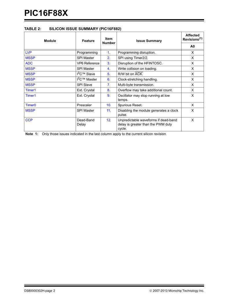
TABLE 2: SILICON ISSUE SUMMARY (PIC16F882)Module Feature Item Number Issue Summary
Affected Revisions(1)
A0
LVP Programming 1. Programming disruption. XMSSP SPI Master 2. SPI using Timer2/2. XADC VP6 Reference 3. Disruption of the HFINTOSC. XMSSP SPI Master 4. Write collision on loading. XMSSP I2C™ Slave 5. R/W bit on ACK. XMSSP I2C™ Master 6. Clock-stretching handling. XMSSP SPI Slave 7. Multi-byte transmission. XTimer1 Ext. Crystal 8. Overflow may take additional count. XTimer1 Ext. Crystal 9. Oscillator may stop running at low
temps.X
Timer0 Prescaler 10. Spurious Reset. XMSSP SPI Master 11. Disabling the module generates a clock
pulse.X
CCP Dead-Band Delay
12. Unpredictable waveforms if dead-band delay is greater than the PWM duty cycle.
X
Note 1: Only those issues indicated in the last column apply to the current silicon revision.
DS80000302H-page 2 2007-2013 Microchip Technology Inc.

PIC16F88X
TABLE 3: SILICON ISSUE SUMMARY (PIC16F883/PIC16F884)Module Feature Item Number Issue Summary
Affected Revisions(1)
A0
LVP Programming 1. Programming disruption. XMSSP SPI Master 2. SPI using Timer2/2. XADC VP6 Reference 3. Disruption of the HFINTOSC. XMSSP SPI Master 4. Write collision on loading. XMSSP I2C™ Slave 5. R/W bit on ACK. XMSSP I2C™ Master 6. Clock-stretching handling. XMSSP SPI Slave 7. Multi-byte transmission. XTimer1 Ext. Crystal 8. Overflow may take additional count. XTimer1 Ext. Crystal 9. Oscillator may stop running at low
temps.X
Timer0 Prescaler 10. Spurious Reset. XMSSP SPI Master 11. Disabling the module generates a clock
pulse.X
CCP Dead-Band Delay
12. Unpredictable waveforms if dead-band delay is greater than the PWM duty cycle.
X
Note 1: Only those issues indicated in the last column apply to the current silicon revision.
2007-2013 Microchip Technology Inc. DS80000302H-page 3
PIC16F88X
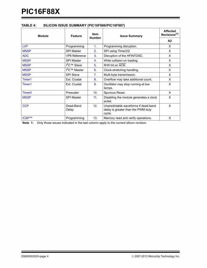
TABLE 4: SILICON ISSUE SUMMARY (PIC16F886/PIC16F887)Module Feature Item Number Issue Summary
Affected Revisions(1)
A2
LVP Programming 1. Programming disruption. XMSSP SPI Master 2. SPI using Timer2/2. XADC VP6 Reference 3. Disruption of the HFINTOSC. XMSSP SPI Master 4. Write collision on loading. XMSSP I2C™ Slave 5. R/W bit on ACK. XMSSP I2C™ Master 6. Clock-stretching handling. XMSSP SPI Slave 7. Multi-byte transmission. XTimer1 Ext. Crystal 8. Overflow may take additional count. XTimer1 Ext. Crystal 9. Oscillator may stop running at low
temps.X
Timer0 Prescaler 10. Spurious Reset. XMSSP SPI Master 11. Disabling the module generates a clock
pulse.X
CCP Dead-Band Delay
12. Unpredictable waveforms if dead-band delay is greater than the PWM duty cycle.
X
ICSP™ Programming 13. Memory read and verify operations. XNote 1: Only those issues indicated in the last column apply to the current silicon revision.
DS80000302H-page 4 2007-2013 Microchip Technology Inc.

PIC16F88X
Silicon Errata Issues1. Module: Low-Voltage In-Circuit Serial Programming™ (LVP)
If LVP (Low-Voltage Programming) mode isenabled, programming the device using the VPPpin while holding high or toggling the port pin RB3/PGM during Program mode could disrupt theprogramming sequence.
Work aroundPull down pin RB3/PGM using external circuitryduring programming of the device.
Affected Silicon Revisions
PIC16F882
PIC16F883/PIC16F884
PIC16F886/PIC16F887
2. Module: MSSP (SPI Mode)
When the SPI is using Timer2/2 as the clocksource, a shorter than expected SCK pulse mayoccur on the first bit of the transmitted/receiveddata (Figure 1).
FIGURE 1: SCK PULSE VARIATION USING TIMER2/2
Work aroundTo avoid producing the short pulse, turn off Timer2and clear the TMR2 register, load SSPBUF withthe data to transmit and then turn Timer2 back on.Refer to Example 1 for sample code.
EXAMPLE 1: AVOIDING THE INITIAL SHORT SCK PULSE
Affected Silicon Revisions
PIC16F882
PIC16F883/PIC16F884
PIC16F886/PIC16F887
Note: This document summarizes all siliconerrata issues from all revisions of silicon,previous as well as current. Only theissues indicated by the shaded column inthe following tables apply to the currentsilicon revision (A0 or A2, as applicable).
A0
X
A0
X
A2
X
A0
X
A0
X
A2
X
SDO
SCK
Write SSPBUF
bit 0 = 1 bit 1 = 0 bit 2 = 1 . . . .
LOOP BTFSS SSPSTAT, BF ;Data received?
;(Xmit complete?)
GOTO LOOP ;No
MOVF SSPBUF, W ;W = SSPBUF
MOVWF RXDATA ;Save in user RAM
MOVF TXDATA, W ;W = TXDATA
BCF T2CON, TMR2ON ;Timer2 off
CLRF TMR2 ;Clear Timer2
MOVWF SSPBUF ;Xmit New data
BSF T2CON, TMR2ON ;Timer2 on
2007-2013 Microchip Technology Inc. DS80000302H-page 5
PIC16F88X
3. Module: Analog-To-Digital Converter(ADC) Module
Selecting the VP6 reference as the analog inputsource (CHS<3:0> = 1111) for the ADCconversion after sampling another analog channelwith input voltages approximately greater than3.6V can temporarily disturb the HFINTOSCoscillator.
Work aroundSelect an ADC channel with input voltages lowerthan 3.6V prior to selecting the VP6 referencevoltage input. Any analog channel can be used,even if that channel is configured as a digital I/O(configured as an output) that is driving the outputpin low. An alternative is to configure the CVREFmodule to output a voltage less than 3.6V and thenselecting that analog channel CHS<3:0> = 1110as the analog input source.
EXAMPLE 2: AVOID DISTURBING THE HFINTOSC OSCILLATOR
Affected Silicon Revisions
PIC16F882
PIC16F883/PIC16F884
PIC16F886/PIC16F887
4. Module: MSSP (SPI Master Mode)
With MSSP in SPI Master mode, FOSC/64 orTimer2/2 clock rate and CKE = 0, a write collisionmay occur if SSPBUF is loaded immediately afterthe transfer is complete. A delay may be requiredafter the MSSP Interrupt Flag bit, SSPIF, is set orthe Buffer Full bit, BF, is set and before writingSSPBUF. If the delay is insufficiently short, a writecollision may occur as indicated by the WCOL bitbeing set.
Work aroundAdd a software delay of one SCK period afterdetecting the completed transfer and prior toupdating the SSPBUF contents. Verify the WCOLbit is clear after writing SSPBUF. If the WCOL isset, clear the bit in software and rewrite theSSPBUF register.
Date Codes that pertain to this issue:All engineering and production devices.
Affected Silicon Revisions
PIC16F882
PIC16F883/PIC16F884
PIC16F886/PIC16F887
Note: This only occurs when selecting theVP6 reference ADC channel using theCHS<3:0> bits in the ADCON0register and NOT during the start of anactual ADC conversion using theGO/DONE bit in the ADCON0 register.
A0
X
A0
X
A2
X
BANKSEL ADCON0 ;
MOVLW B’XX111001’ ;Select ADC
MOVWF ADCON0 ;Channel CVREF
MOVLW B’XX111101’ ;Select ADC
MOVWF ADCON0 ;Channel VP6
A0
X
A0
X
A2
X
DS80000302H-page 6 2007-2013 Microchip Technology Inc.

PIC16F88X
5. Module: MSSP (I2C™ Slave Mode)When the master device wants to terminatereceiving any more data from the slave device, itwill do so by sending a NACK in response to thelast data byte received from the slave. When theslave receives the NACK, the R/W bit of theSSPSTAT register remains set improperly.
Work aroundUse the CKP bit of the SSPCON register todetermine when the master has responded with aNACK. The CKP bit will be clear when theresponse is an ACK, and set when the response isa NACK. The CKP bit is automatically cleared tostretch the clock when the master responds toreceived data with an ACK. This gives the slavetime to load the SSPBUF register before settingthe CKP bit to release the clock stretching. Whenthe master responds to received data with aNACK, the CKP bit properly remains set and thereis no clock stretching.
Affected Silicon Revisions
PIC16F882
PIC16F883/PIC16F884
PIC16F886/PIC16F887
A0
X
A0
X
A2
X
2007-2013 Microchip Technology Inc. DS80000302H-page 7
PIC16F88X
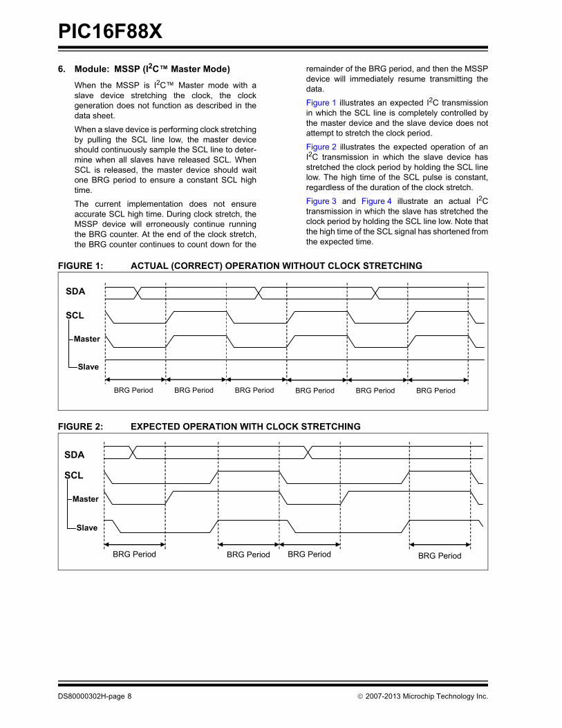
6. Module: MSSP (I2C™ Master Mode)When the MSSP is I2C™ Master mode with aslave device stretching the clock, the clockgeneration does not function as described in thedata sheet.
When a slave device is performing clock stretchingby pulling the SCL line low, the master deviceshould continuously sample the SCL line to deter-mine when all slaves have released SCL. WhenSCL is released, the master device should waitone BRG period to ensure a constant SCL hightime.
The current implementation does not ensureaccurate SCL high time. During clock stretch, theMSSP device will erroneously continue runningthe BRG counter. At the end of the clock stretch,the BRG counter continues to count down for the
remainder of the BRG period, and then the MSSPdevice will immediately resume transmitting thedata.
Figure 1 illustrates an expected I2C transmissionin which the SCL line is completely controlled bythe master device and the slave device does notattempt to stretch the clock period.
Figure 2 illustrates the expected operation of anI2C transmission in which the slave device hasstretched the clock period by holding the SCL linelow. The high time of the SCL pulse is constant,regardless of the duration of the clock stretch.
Figure 3 and Figure 4 illustrate an actual I2Ctransmission in which the slave has stretched theclock period by holding the SCL line low. Note thatthe high time of the SCL signal has shortened fromthe expected time.
FIGURE 1: ACTUAL (CORRECT) OPERATION WITHOUT CLOCK STRETCHING
FIGURE 2: EXPECTED OPERATION WITH CLOCK STRETCHING
BRG Period BRG Period BRG Period BRG Period BRG Period BRG Period
SDA
SCL
Master
Slave
BRG Period BRG Period BRG Period BRG Period
SDA
SCL
Master
Slave
DS80000302H-page 8 2007-2013 Microchip Technology Inc.

PIC16F88X
FIGURE 3: ACTUAL (INCORRECT) OPERATION WITH CLOCK STRETCHING – EXAMPLE 1FIGURE 4: ACTUAL (INCORRECT) OPERATION WITH CLOCK STRETCHING – EXAMPLE 2
Work aroundSet the communication speed to match theslowest device on the bus. This ensures that noslave device will perform clock stretching.
It is possible to dynamically adjust thecommunication speed to match the device beingaddressed by modifying the BRG register.However, the behavior of slower slave devicesmust be understood and speed adjustments madesuch that no slave performs clock stretching.
Affected Silicon Revisions
PIC16F882
PIC16F883/PIC16F884
PIC16F886/PIC16F887
SDA
SCL
Master
Slave
BRG Period BRG Period BRG Period BRG Period BRG Period BRG Period
SDA
SCL
Master
Slave
BRG Period BRG Period BRG Period BRG Period BRG Period BRG Period
A0
X
A0
X
A2
X
2007-2013 Microchip Technology Inc. DS80000302H-page 9
PIC16F88X
7. Module: MSSPWhen all of the following conditions are met:
1. The module is configured as a SPI slave2. CKP = 13. CKE = 14. Multiple bytes are sent to the Slave with the
SS line remaining low between bytes
The SSPIF flag will only be set on reception of thefirst byte and the following bytes will not becorrectly received.
Work around• SPI Master toggles the SS line between bytes
or
• On reception of the first byte, modify the SSPM0 bit in the SSPCON register to configure the module as a SPI slave with SS pin disabled. Then, restore the SSPM0 bit to the configuration for SPI slave with SS pin enabled. The module is then ready for reception of the following byte.
Affected Silicon Revisions
PIC16F882
PIC16F883/PIC16F884
PIC16F886/PIC16F887
A0
X
A0
X
A2
X
BSF SSPCON, SSPM0
BCF SSPCON, SSPM0
DS80000302H-page 10 2007-2013 Microchip Technology Inc.
PIC16F88X
8. Module: Asynchronous Timer1This Errata supersedes Errata DS80233 andDS80329.
When TImer1 is started or updated, the timerneeds to see a falling edge from the external clocksource before a rising edge can increment thecounter. If writes to TMR1H and TMR1L are notcompleted while the external clock pulse is stillhigh, Timer1 will not count the first clock pulse afterthe update.
When using an external crystal, the pulse widthfrom rising to falling edge is temperature-dependent and may decrease with temperature.As a result, the timer may require an additionaloscillation to overflow.
Work aroundSwitching to the HFINTOSC after reloading, thetimer ensures the Timer1 will see a falling edgebefore switching back to the external clock source.
Due to the time from Timer1 overflow to the reloadbeing application specific, wait for the timer toincrement before beginning the reload sequence.This ensures the timer does not miss a rising edgeduring reload.
EXAMPLE 3:
Affected Silicon Revisions
PIC16F882
PIC16F883/PIC16F884
PIC16F886/PIC16F887
BTFSC TMR1L,0
GOTO $-1
BTFSS TMR1L,0
GOTO $-1 ;Timer has just incremented, 31 s before next rising edge to;complete reload
Update:
BCF T1CON,TMR1CS ;Select HFINTOSC for Timer1
BSF TMR1H,7 ;Timer1 high byte 0x80
BCF T1CON,TMR1ON ;Timer1 off
BSF T1CON,TMR1CS ;Select external crystal
BCF T1CON,TMR1ON ;Timer1 on
Critical Timing of code sequence for instructions following last write to TMR1L or TMR1H.
A0
X
A0
X
A2
X
2007-2013 Microchip Technology Inc. DS80000302H-page 11

PIC16F88X
9. Module: LP/Timer1 Oscillator OperationBelow 25°C1-2% of devices experience reduced drive astemperatures approach -40°C. This will result in aloss of Timer1 counts or stopped Timer1oscillation.
This can also prevent Timer1 oscillator start-upunder cold conditions.
Work aroundUse of low-power crystals properly matched to thedevice will reduce the likelihood of failure. A 1 mresister between OSC2 and VDD will furtherimprove the drive strength of the circuit.
Affected Silicon Revisions
PIC16F882
PIC16F883/PIC16F884
PIC16F886/PIC16F887
10. Module: Timer0 and WDT Prescaler Assignment Spurious Reset
A spurious Reset may occur if the Timer0/Watchdog Timer (WDT) prescaler is assigned fromthe WDT to Timer0 and then back to the WDT.
SummaryThe issue only arises when all of the below condi-tions are met:
• Timer0 external clock input (T0CKI) is enabled.
• The Prescaler is assigned to the WDT, then to the Timer0 and back to the WDT.
• During the assignments, the T0CKI pin is high when bit T0SE is set, or low when T0SE is clear.
• The 1:1 Prescaler option is chosen.
DescriptionOn a POR, the Timer0/WDT prescaler is assignedto the WDT.
If the prescaler is reassigned to Timer0 and Timer0external clock input (T0CKI) is enabled then theprescaler would be clocked by a transition on theT0CKI pin.
On power-up, the T0CKI pin is (by default) enabledfor Timer0 in the OPTION register.
If the T0CKI pin is:
• High and Timer0 is configured to transition on a falling edge (T0SE set), or
• Low and Timer0 is configured to transition on a rising edge (T0SE clear)
Then, if the prescaler is reassigned to the WDT, aclock pulse to the prescaler will be generated onthe reassignment.
If the prescaler is configured for the 1:1 option, theclock pulse will incorrectly cause a WDT Time-outReset of the device.
Work around1. Disable the Timer0 external clock input by
clearing the T0CKI bit in the OPTIONregister.
2. Modify the T0SE bit in the OPTION register tothe opposite configuration for the logic levelon the T0CKI pin.
3. Select a prescaler rate other than 1:1 andissue a CLRWDT instruction before switchingto the final prescaler rate.
Affected Silicon Revisions
PIC16F882
PIC16F883/PIC16F884
PIC16F886/PIC16F887
A0
X
A0
X
A2
X
A0
X
A0
X
A2
X
DS80000302H-page 12 2007-2013 Microchip Technology Inc.
PIC16F88X
11. Module: MSSP (SPI Master Mode)When the MSSP module is configured as a SPImaster with CKP set, (SPI clock idles high)disabling the module by clearing the SSPEN bitwill cause the clock line to be driven low for 2 TOSCbefore the setting of the RC3 output in the PORTCregister takes effect.
Similarly on enabling the module. There is a 1TOSC period where the clock line will be driven lowbefore the CKP bit takes effect and the line isdriven high.
Work aroundA pull-up resistor on the SCK line allows the pin tobe configured as high-impedance during disabling/enabling the module and the line to be pulled highby the resistor.
The TRISC3 bit should be set before disabling orenabling the module to tristate the pin, and thencleared before transmission.
Affected Silicon Revisions
PIC16F882
PIC16F883/PIC16F884
PIC16F886/PIC16F887
12. Module: Capture Compare PWM (CCP)
With the ECCP configured for PWM Half-Bridgemode and a dead-band delay greater than or equalto the PWM duty cycle, unpredictable waveformswill result.
Work aroundMake sure the dead-band delay is always lessthan the PWM duty cycle.
Affected Silicon Revisions
PIC16F882
PIC16F883/PIC16F884
PIC16F886/PIC16F887
13. Module: ICSP
If the supply voltage (VDD) applied to the device isbelow 2.7V, the device can misread memorylocations while performing an In-Circuit SerialProgramming™ (ICSP™) read or verify commandof the Program Flash Memory (PFM) or the DataEEPROM. This errata applies to both the High-Voltage ICSP and the Low-Voltage ICSP modes ofthe device, as described in the “PIC16F88XMemory Programming Specification” (DS41287).This low-voltage memory misread issue is limitedto only the ICSP hardware interface module on thedevice, which is only used during deviceprogramming. In Normal user mode, the devicewill operate properly down to the specified VDDsupply limits, as documented in the device datasheet (“PIC16F882/883/884/886/887, 28/40/44-Pin Flash-Based, 8-Bit CMOS Microcontrollers)’’’(DS41291).
Work aroundMaintain a minimum VDD voltage setting of 2.7V orabove when performing an ICSP read or verifycommand during programming of the PFM or DataEEPROM Memory.
PIC16F886/PIC16F887
A0
X
A0
X
A2
X
A0
X
A0
X
A2
X
A2
X
2007-2013 Microchip Technology Inc. DS80000302H-page 13
PIC16F88X
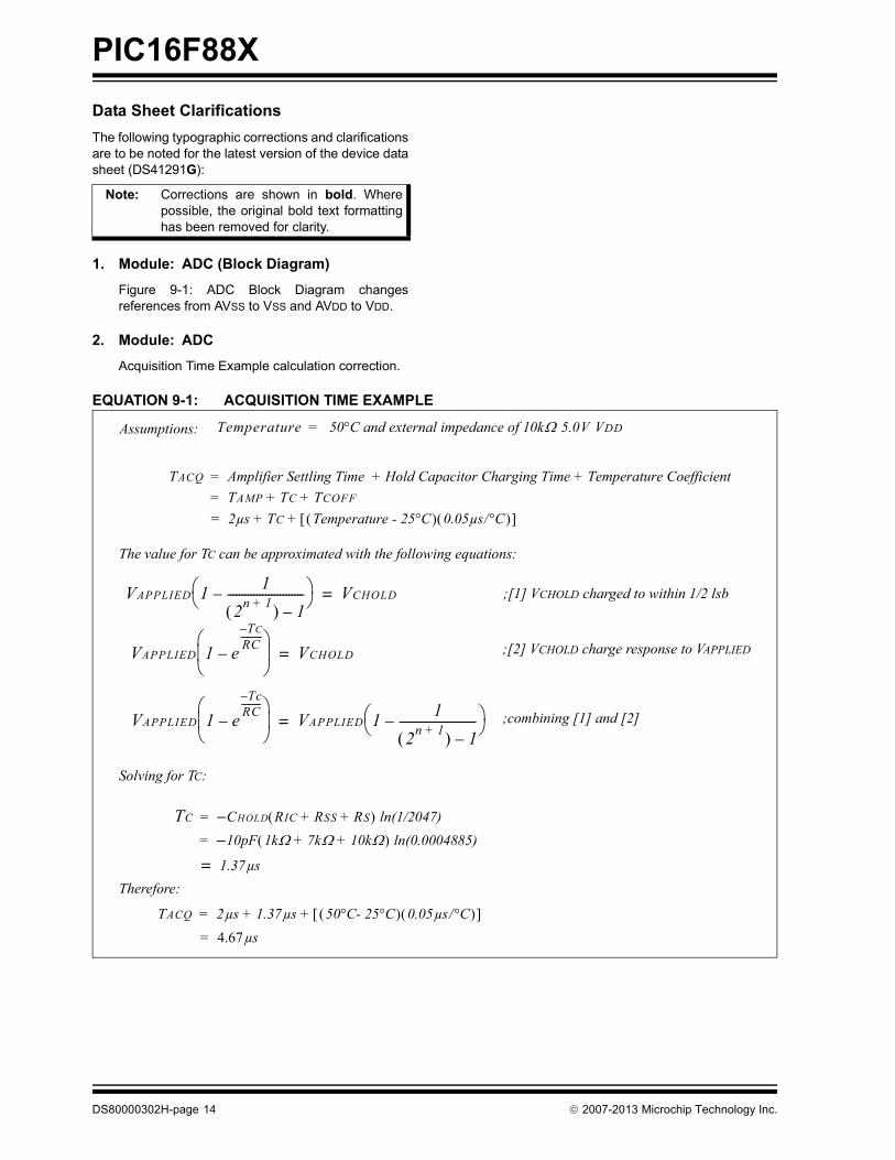
Data Sheet ClarificationsThe following typographic corrections and clarificationsare to be noted for the latest version of the device datasheet (DS41291G):1. Module: ADC (Block Diagram)
Figure 9-1: ADC Block Diagram changesreferences from AVSS to VSS and AVDD to VDD.
2. Module: ADC
Acquisition Time Example calculation correction.
EQUATION 9-1: ACQUISITION TIME EXAMPLE
Note: Corrections are shown in bold. Wherepossible, the original bold text formattinghas been removed for clarity.
TACQ Amplifier Settling Time Hold Capacitor Charging Time Temperature Coefficient+ += TAMP TC TCOFF+ += 2µs TC Temperature - 25°C 0.05µs/°C + +=
TC CHOLD RIC RSS RS+ + ln(1/2047)–= 10pF 1k 7k 10k+ + – ln(0.0004885)=
1.37= µs
TACQ 2µs 1.37µs 50°C- 25°C 0.05µs/°C + += 4.67µs=
VAPPLIED 1 eTc–
RC---------–
VAPPLIED 1 12n 1+ 1–
--------------------------– =
VAPPLIED 1 12n 1+ 1–
--------------------------– VCHOLD=
VAPPLIED 1 eTC–
RC----------–
VCHOLD=
;[1] VCHOLD charged to within 1/2 lsb
;[2] VCHOLD charge response to VAPPLIED
;combining [1] and [2]
The value for TC can be approximated with the following equations:
Solving for TC:
Therefore:
Temperature 50°C and external impedance of 10k 5.0V VDD=Assumptions:
DS80000302H-page 14 2007-2013 Microchip Technology Inc.

PIC16F88X
APPENDIX A: DOCUMENT REVISION HISTORY
REV. A DOCUMENT (2/2007)First revision of this document.
Added Module 1: Low-Voltage In-Circuit SerialProgramming™ (PIC16F884/883 Silicon Rev. A0);Added Module 2: MSSP (SPI Mode).
Clarifications/Corrections to the Data Sheet – AddedModule 1: Product Identification System.
REV. B DOCUMENT (5/2007)Clarifications/Corrections to the Data Sheet – AddedModule 2: Electrical Specification - Supply Current.
REV. C DOCUMENT (7/2007)Added Module 3: Analog-to-Digital Converter (ADC)Module.
REV. D DOCUMENT (8/2007)Added Module 4: MSSP (SPI Master Mode), Module 5:MSSP (I2C Slave Mode) and Module 6: MSSP (I2CMaster Mode).
REV. E DOCUMENT (4/2009)Updated Errata to new format.
Data Sheet Clarification: Added Module 1: Timer1(Block Diagram); Module 2: Comparator (C2 BlockDiagram); Module 3: ADC (Block Diagram); Module 4:Comparator Voltage Reference; Module 5: ComparatorVoltage Reference.
Added Module 7: MSSP; Added Module 8:Asynchronous Timer1; Added Module 9: LP/Timer1Oscillator Operation Below 25C; Module 10: Timer0and WDT Prescaler Assignment Spurious Reset.
REV. F DOCUMENT (8/2009)Added Module 11: MSSP (SPI Master Mode); UpdatedTables 2, 3, 4.
Data Sheet Clarification: Removed Modules 1, 2, 4 and5 as the Data Sheet has already been updatedaccording to this version of the errata.
Added Module 2: ADC.
REV. G DOCUMENT (12/2012)Added Module 12: Capture Compare PWM (CCP).
REV. H DOCUMENT (8/2013)Added Module 13: ICSP; Other minor corrections.
2007-2013 Microchip Technology Inc. DS80000302H-page 15

PIC16F88X
NOTES:DS80000302H-page 16 2007-2013 Microchip Technology Inc.

Note the following details of the code protection feature on Microchip devices:• Microchip products meet the specification contained in their particular Microchip Data Sheet.
• Microchip believes that its family of products is one of the most secure families of its kind on the market today, when used in the intended manner and under normal conditions.
• There are dishonest and possibly illegal methods used to breach the code protection feature. All of these methods, to our knowledge, require using the Microchip products in a manner outside the operating specifications contained in Microchip’s Data Sheets. Most likely, the person doing so is engaged in theft of intellectual property.
• Microchip is willing to work with the customer who is concerned about the integrity of their code.
• Neither Microchip nor any other semiconductor manufacturer can guarantee the security of their code. Code protection does not mean that we are guaranteeing the product as “unbreakable.”
Code protection is constantly evolving. We at Microchip are committed to continuously improving the code protection features of ourproducts. Attempts to break Microchip’s code protection feature may be a violation of the Digital Millennium Copyright Act. If such actsallow unauthorized access to your software or other copyrighted work, you may have a right to sue for relief under that Act.
Information contained in this publication regarding deviceapplications and the like is provided only for your convenienceand may be superseded by updates. It is your responsibility toensure that your application meets with your specifications.MICROCHIP MAKES NO REPRESENTATIONS ORWARRANTIES OF ANY KIND WHETHER EXPRESS ORIMPLIED, WRITTEN OR ORAL, STATUTORY OROTHERWISE, RELATED TO THE INFORMATION,INCLUDING BUT NOT LIMITED TO ITS CONDITION,QUALITY, PERFORMANCE, MERCHANTABILITY ORFITNESS FOR PURPOSE. Microchip disclaims all liabilityarising from this information and its use. Use of Microchipdevices in life support and/or safety applications is entirely atthe buyer’s risk, and the buyer agrees to defend, indemnify andhold harmless Microchip from any and all damages, claims,suits, or expenses resulting from such use. No licenses areconveyed, implicitly or otherwise, under any Microchipintellectual property rights.
2007-2013 Microchip Technology Inc.
QUALITY MANAGEMENT SYSTEM CERTIFIED BY DNV
== ISO/TS 16949 ==
Trademarks
The Microchip name and logo, the Microchip logo, dsPIC, FlashFlex, KEELOQ, KEELOQ logo, MPLAB, PIC, PICmicro, PICSTART, PIC32 logo, rfPIC, SST, SST Logo, SuperFlash and UNI/O are registered trademarks of Microchip Technology Incorporated in the U.S.A. and other countries.
FilterLab, Hampshire, HI-TECH C, Linear Active Thermistor, MTP, SEEVAL and The Embedded Control Solutions Company are registered trademarks of Microchip Technology Incorporated in the U.S.A.
Silicon Storage Technology is a registered trademark of Microchip Technology Inc. in other countries.
Analog-for-the-Digital Age, Application Maestro, BodyCom, chipKIT, chipKIT logo, CodeGuard, dsPICDEM, dsPICDEM.net, dsPICworks, dsSPEAK, ECAN, ECONOMONITOR, FanSense, HI-TIDE, In-Circuit Serial Programming, ICSP, Mindi, MiWi, MPASM, MPF, MPLAB Certified logo, MPLIB, MPLINK, mTouch, Omniscient Code Generation, PICC, PICC-18, PICDEM, PICDEM.net, PICkit, PICtail, REAL ICE, rfLAB, Select Mode, SQI, Serial Quad I/O, Total Endurance, TSHARC, UniWinDriver, WiperLock, ZENA and Z-Scale are trademarks of Microchip Technology Incorporated in the U.S.A. and other countries.
SQTP is a service mark of Microchip Technology Incorporated in the U.S.A.
GestIC and ULPP are registered trademarks of Microchip Technology Germany II GmbH & Co. KG, a subsidiary of Microchip Technology Inc., in other countries.
All other trademarks mentioned herein are property of their respective companies.
© 2007-2013, Microchip Technology Incorporated, Printed in the U.S.A., All Rights Reserved.
Printed on recycled paper.
ISBN: 9781620773963
Microchip received ISO/TS-16949:2009 certification for its worldwide
DS80000302H-page 17
headquarters, design and wafer fabrication facilities in Chandler and Tempe, Arizona; Gresham, Oregon and design centers in California and India. The Company’s quality system processes and procedures are for its PIC® MCUs and dsPIC® DSCs, KEELOQ® code hopping devices, Serial EEPROMs, microperipherals, nonvolatile memory and analog products. In addition, Microchip’s quality system for the design and manufacture of development systems is ISO 9001:2000 certified.
DS80000302H-page 18 2007-2013 Microchip Technology Inc.
AMERICASCorporate Office2355 West Chandler Blvd.Chandler, AZ 85224-6199Tel: 480-792-7200 Fax: 480-792-7277Technical Support: http://www.microchip.com/supportWeb Address: www.microchip.comAtlantaDuluth, GA Tel: 678-957-9614 Fax: 678-957-1455BostonWestborough, MA Tel: 774-760-0087 Fax: 774-760-0088ChicagoItasca, IL Tel: 630-285-0071 Fax: 630-285-0075ClevelandIndependence, OH Tel: 216-447-0464 Fax: 216-447-0643DallasAddison, TX Tel: 972-818-7423 Fax: 972-818-2924DetroitFarmington Hills, MI Tel: 248-538-2250Fax: 248-538-2260IndianapolisNoblesville, IN Tel: 317-773-8323Fax: 317-773-5453Los AngelesMission Viejo, CA Tel: 949-462-9523 Fax: 949-462-9608Santa ClaraSanta Clara, CA Tel: 408-961-6444Fax: 408-961-6445TorontoMississauga, Ontario, CanadaTel: 905-673-0699 Fax: 905-673-6509
ASIA/PACIFICAsia Pacific OfficeSuites 3707-14, 37th FloorTower 6, The GatewayHarbour City, KowloonHong KongTel: 852-2401-1200Fax: 852-2401-3431Australia - SydneyTel: 61-2-9868-6733Fax: 61-2-9868-6755China - BeijingTel: 86-10-8569-7000 Fax: 86-10-8528-2104China - ChengduTel: 86-28-8665-5511Fax: 86-28-8665-7889China - ChongqingTel: 86-23-8980-9588Fax: 86-23-8980-9500China - HangzhouTel: 86-571-2819-3187 Fax: 86-571-2819-3189China - Hong Kong SARTel: 852-2943-5100 Fax: 852-2401-3431China - NanjingTel: 86-25-8473-2460Fax: 86-25-8473-2470China - QingdaoTel: 86-532-8502-7355Fax: 86-532-8502-7205China - ShanghaiTel: 86-21-5407-5533 Fax: 86-21-5407-5066China - ShenyangTel: 86-24-2334-2829Fax: 86-24-2334-2393China - ShenzhenTel: 86-755-8864-2200 Fax: 86-755-8203-1760China - WuhanTel: 86-27-5980-5300Fax: 86-27-5980-5118China - XianTel: 86-29-8833-7252Fax: 86-29-8833-7256China - XiamenTel: 86-592-2388138 Fax: 86-592-2388130China - ZhuhaiTel: 86-756-3210040 Fax: 86-756-3210049
ASIA/PACIFICIndia - BangaloreTel: 91-80-3090-4444 Fax: 91-80-3090-4123India - New DelhiTel: 91-11-4160-8631Fax: 91-11-4160-8632India - PuneTel: 91-20-2566-1512Fax: 91-20-2566-1513Japan - OsakaTel: 81-6-6152-7160 Fax: 81-6-6152-9310Japan - TokyoTel: 81-3-6880- 3770 Fax: 81-3-6880-3771Korea - DaeguTel: 82-53-744-4301Fax: 82-53-744-4302Korea - SeoulTel: 82-2-554-7200Fax: 82-2-558-5932 or 82-2-558-5934Malaysia - Kuala LumpurTel: 60-3-6201-9857Fax: 60-3-6201-9859Malaysia - PenangTel: 60-4-227-8870Fax: 60-4-227-4068Philippines - ManilaTel: 63-2-634-9065Fax: 63-2-634-9069SingaporeTel: 65-6334-8870Fax: 65-6334-8850Taiwan - Hsin ChuTel: 886-3-5778-366Fax: 886-3-5770-955Taiwan - KaohsiungTel: 886-7-213-7828Fax: 886-7-330-9305Taiwan - TaipeiTel: 886-2-2508-8600 Fax: 886-2-2508-0102Thailand - BangkokTel: 66-2-694-1351Fax: 66-2-694-1350
EUROPEAustria - WelsTel: 43-7242-2244-39Fax: 43-7242-2244-393Denmark - CopenhagenTel: 45-4450-2828 Fax: 45-4485-2829France - ParisTel: 33-1-69-53-63-20 Fax: 33-1-69-30-90-79Germany - MunichTel: 49-89-627-144-0 Fax: 49-89-627-144-44Italy - Milan Tel: 39-0331-742611 Fax: 39-0331-466781Netherlands - DrunenTel: 31-416-690399 Fax: 31-416-690340Spain - MadridTel: 34-91-708-08-90Fax: 34-91-708-08-91UK - WokinghamTel: 44-118-921-5869Fax: 44-118-921-5820
Worldwide Sales and Service
11/29/12


![SAMA5D2 Family Silicon Errata and Data Sheet Clarification........continued Part Number Silicon Revision Device Identification CHIPID_CIDR[31:0] CHIPID_EXID[31:0] ATSAMA5D22C-CN C](https://img.dokumen.tips/doc/110x75/60a9c81cbab8cb07944ab11b/sama5d2-family-silicon-errata-and-data-sheet-clarification-continued-part.jpg)