Embed Size (px)
DESCRIPTION
Cbse project logic gates
Citation preview

1 | P a g e
CERTIFICATE
This is to certify that <name> of class XII has satisfactorily completed the project on “LOGIC GATES” under the guidance of <teachers name>during the session 2013-2014.

2 | P a g e
VALUED BY
TEACHER EXTERNAL EXAMINER
PRINCIPAL

3 | P a g e
DATE:
ACKNOWLEDGMENT
I'd like to express my greatest gratitude to the people who have helped & supported me throughout my project. I’ m grateful to our school’s PHYSICS faculty
I thank <teachers name> for her continuous support for the project, from initial advice & encouragement to this day. Special thanks of mine goes to my colleagues who helped me in completing the project by giving
necessary
information on the apparatus used in this
experiment, made this project easy and
accurate.

4 | P a g e
I wish to thank my parents for their undivided support & interest who inspired me & encouraged me to go my own way without which I would be unable to complete my project. At last but not the least I want to thanks my friends who appreciated me for my work & motivated
me.
CONTENT•Introduction
• Experiment
1. Aim 10

5 | P a g e
2. Apparatus 10
3. Theory 11
4. Procedure 16
5. Circuits Prepared 22
6. Observations 24
7. Result 26
6 | P a g e
Bibliography 27
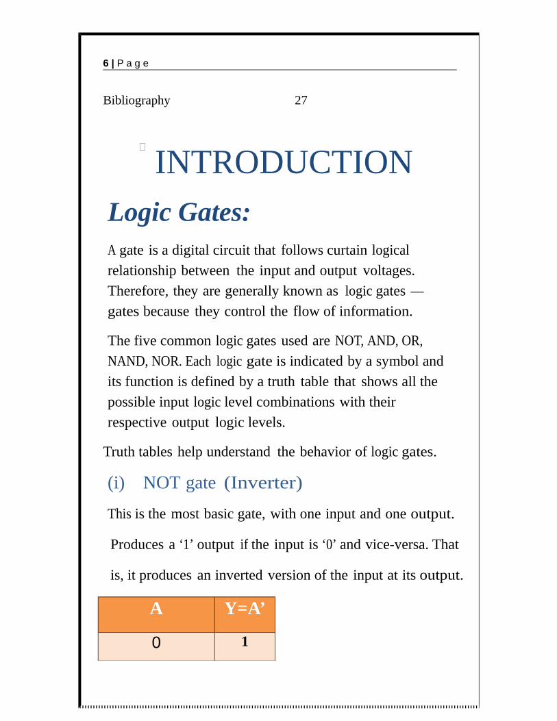
INTRODUCTION
Logic Gates:A gate is a digital circuit that follows curtain logical
relationship between the input and output voltages.
Therefore, they are generally known as logic gates —
gates because they control the flow of information.
The five common logic gates used are NOT, AND, OR,
NAND, NOR. Each logic gate is indicated by a symbol and
its function is defined by a truth table that shows all the
possible input logic level combinations with their
respective output logic levels.
Truth tables help understand the behavior of logic gates.
(i) NOT gate (Inverter)
This is the most basic gate, with one input and one output.
Produces a ‘1’ output if the input is ‘0’ and vice-versa. That
is, it produces an inverted version of the input at its output.
A Y=A’
0 1

7 | P a g e
1 0
(ii) OR Gate
An OR gate has two or more inputs with one output. The output Y is 1 when either input A or input B or both are 1s, that is, if any of the input is high, the output is high.
A B Y=A OR B(A+B)0 0 00 1 11 0 11 1 1
(iii) AND Gate
An AND gate has two or more inputs and one output. The output Y of AND gate is 1 ,only when input A and input B are both 1. It kind of looks for the minimum of the two signals.
A B Y=A AND B(A.B)
0 0 00 1 0

8 | P a g e
1 0 01 1 1
1

Some Basic Logic Gates and Their Truth Tables
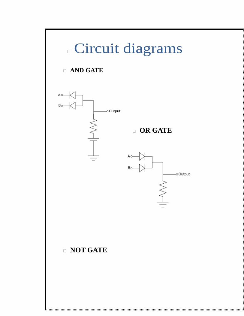
Circuit diagrams AND GATE
OR GATE
NOT GATE
Experiment
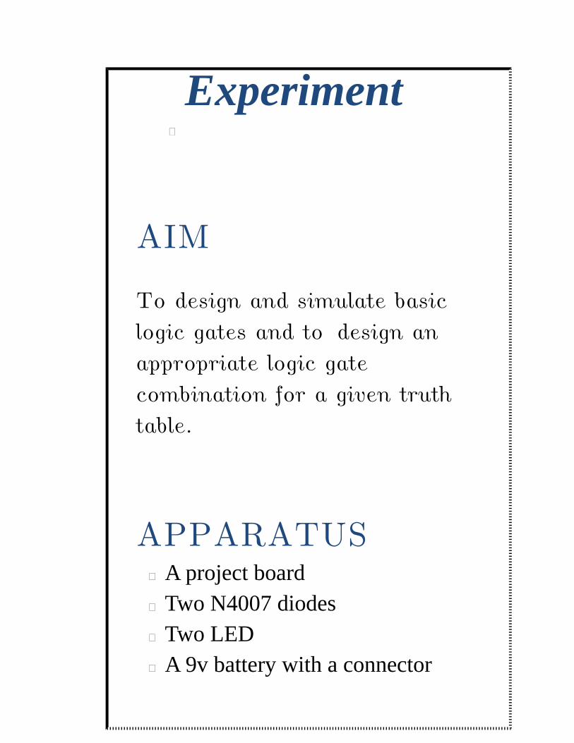
AIM
To design and simulate basic logic gates and to design an appropriate logic gate combination for a given truth table.
APPARATUS A project board Two N4007 diodes Two LED A 9v battery with a connector
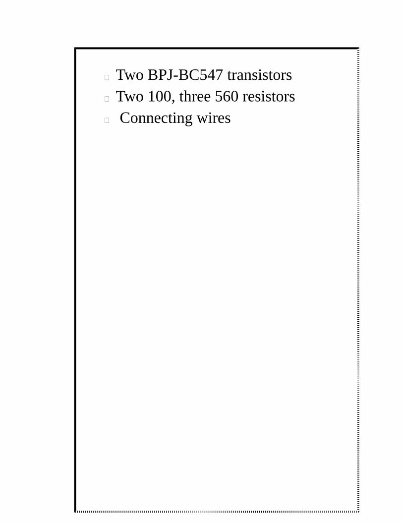
Two BPJ-BC547 transistors Two 100, three 560 resistors Connecting wires
THEORY
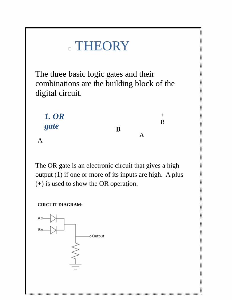
The three basic logic gates and their combinations are the building block of the digital circuit.
1. OR gate
A
BA
+B
The OR gate is an electronic circuit that gives a high output (1) if one or more of its inputs are high. A plus (+) is used to show the OR operation.
CIRCUIT DIAGRAM:


2. AND Gate
A A.B
B
The AND gate is an electronic circuit that gives high output only if all inputs are high
CIRCUIT DIAGRAM :
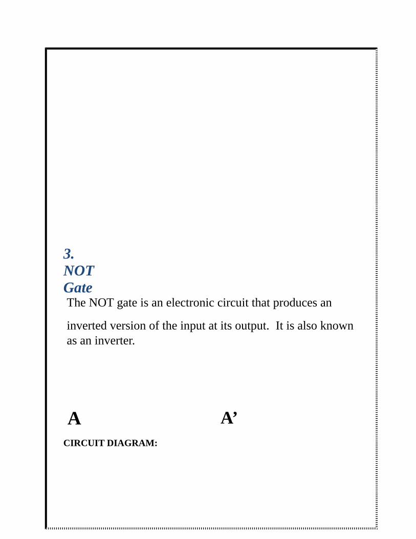
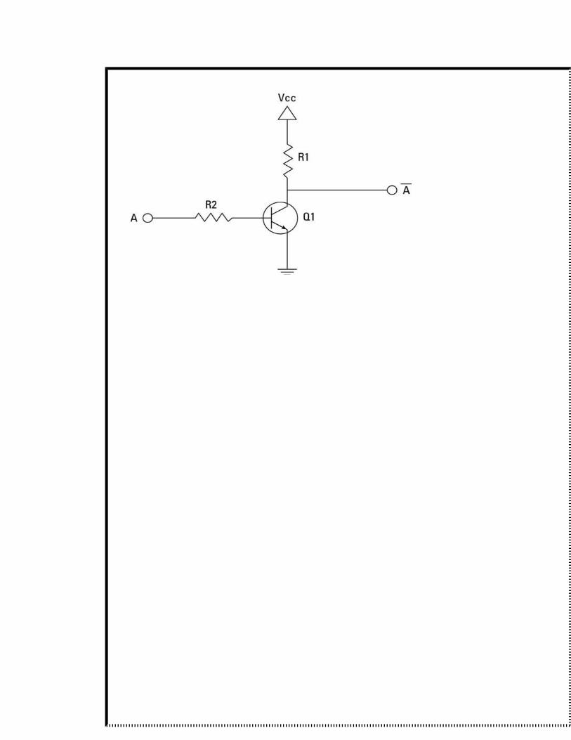
3. NOT GateThe NOT gate is an electronic circuit that produces an
inverted version of the input at its output. It is also known as an inverter.
A A’CIRCUIT DIAGRAM:

0
1

PROCEDURE
Design of basic logic gates.
DESIGN OF AND GATE
COMPONENTS: Two p-n junction diode, A LED, A 100 resistors
CONSTRUCTION: An AND gate can be realized by connecting the diodes as shown in the figure. A resistance of 100 is connected in series with the LED to prevent its malfunction.
PROJECT BOARD CIRCUIT:
GROUND
HIGH

DESIGN OF OR GATE
COMPONENTS: Two p-n junction diode, A LED, A 100 resistors
CONSTRUCTION: An OR gate can be realized by connecting the diodes as shown in the figure. Here also there is a need for a 100 resistor in series with LED
PROJECT BOARD CIRCUIT:
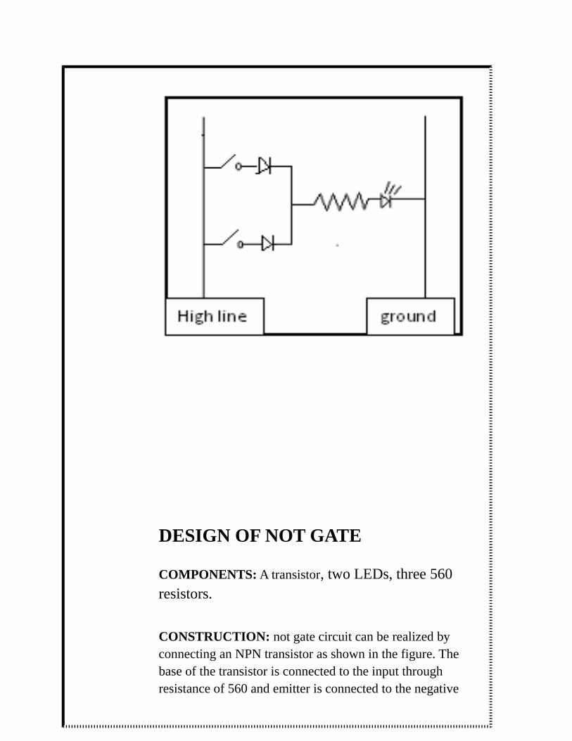
DESIGN OF NOT GATE
COMPONENTS: A transistor, two LEDs, three 560 resistors.
CONSTRUCTION: not gate circuit can be realized by connecting an NPN transistor as shown in the figure. The base of the transistor is connected to the input through resistance of 560 and emitter is connected to the negative
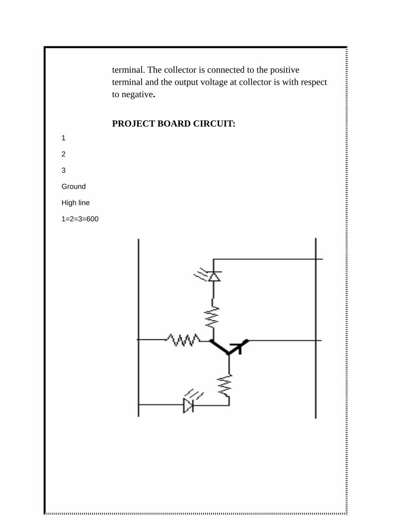
terminal. The collector is connected to the positive terminal and the output voltage at collector is with respect to negative.
PROJECT BOARD CIRCUIT:
1
2
3
Ground
High line
1=2=3=600

Logic gate combination for given truth table
1. Write product term for each input (minterm), Combination where Boolean function has output
2. While writing minterms, complement the variable whose value is 0 otherwise write it in the direct form (without complement).
3. Add all the minterms to obtain the Boolean function.
3. Draw the circuit using basic LOGIC Gates.
So we, choose the given Truth Table.
A B Y=A.B Y’
0 0 0 1
0 1 0 1
1 0 0 1
1 1 1 0
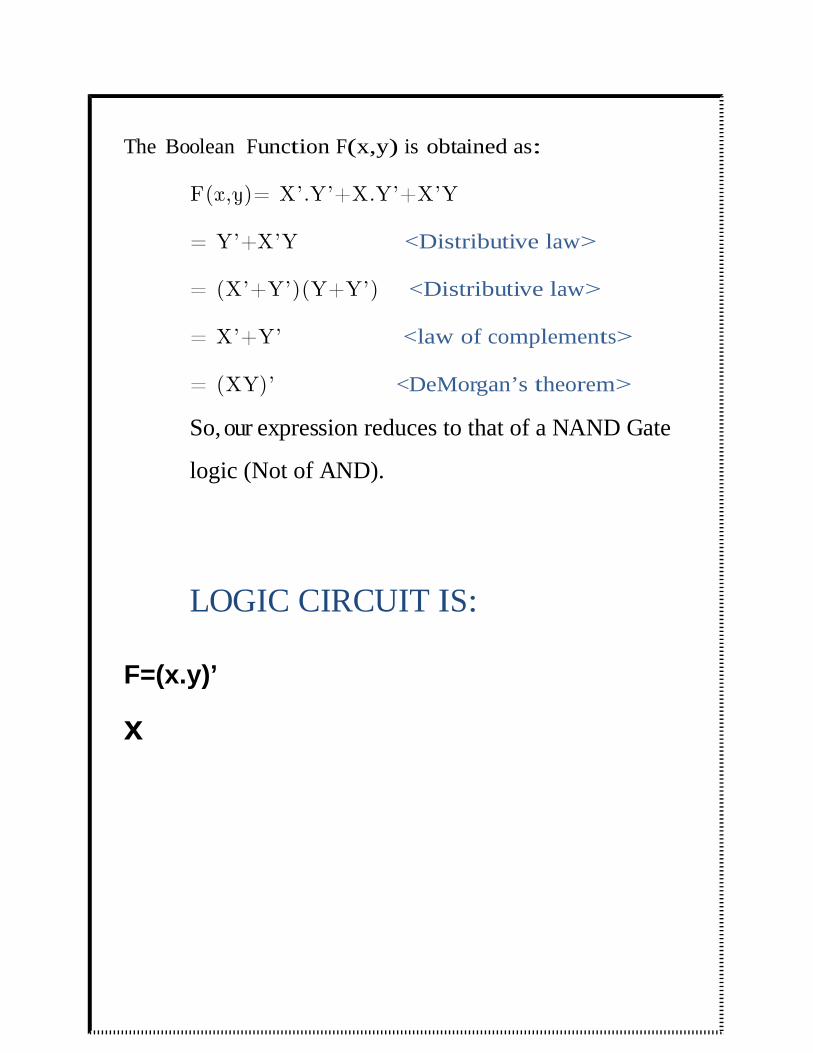
The Boolean Function F(x,y) is obtained as:
F(x,y)= X’.Y’+X.Y’+X’Y
= Y’+X’Y <Distributive law>
= (X’+Y’)(Y+Y’) <Distributive law>
= X’+Y’ <law of complements>
= (XY)’ <DeMorgan’s theorem>
So, our expression reduces to that of a NAND Gate
logic (Not of AND).
LOGIC CIRCUIT IS:
F=(x.y)’
x
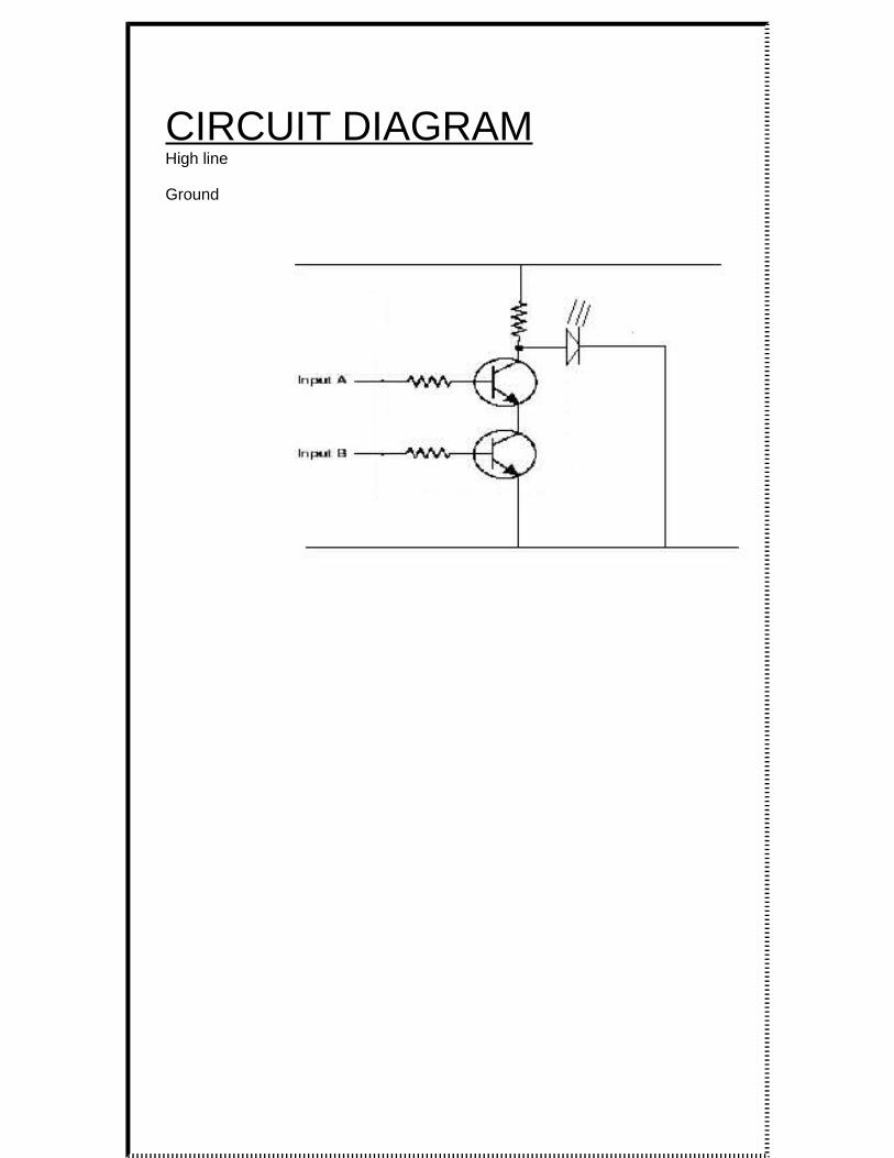
CIRCUIT DIAGRAMHigh line
Ground
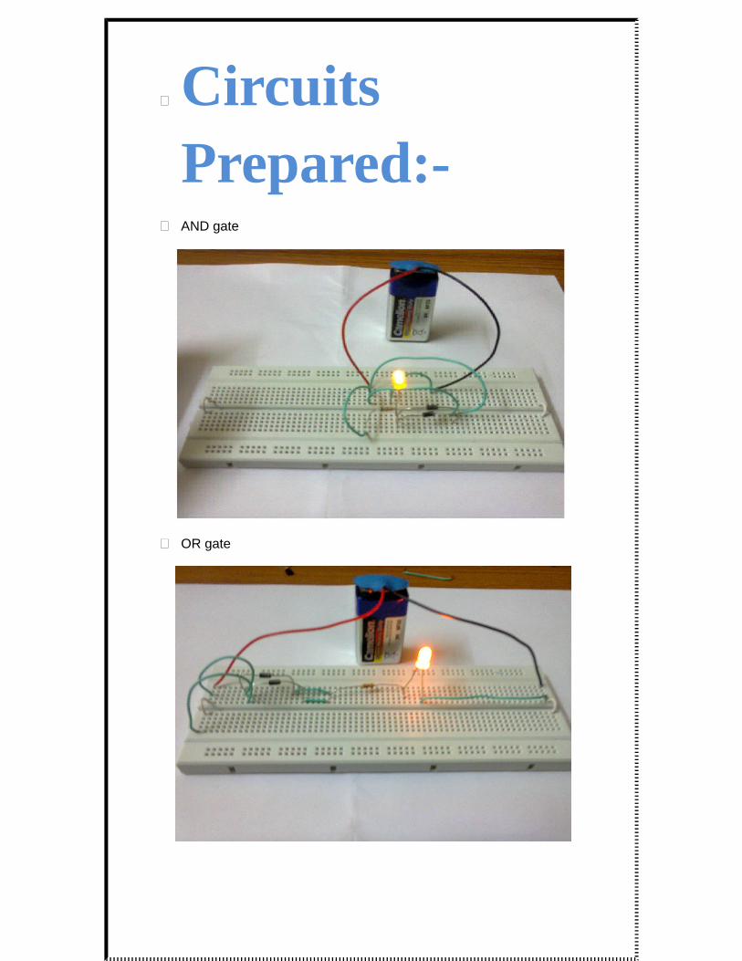
Circuits Prepared:-
AND gate
OR gate
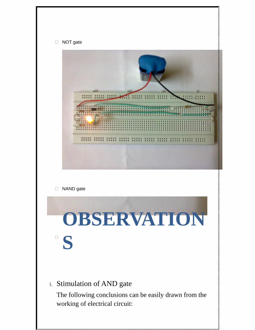
NOT gate
NAND gate
OBSERVATIONS
1. Stimulation of AND gate
The following conclusions can be easily drawn from the working of electrical circuit:
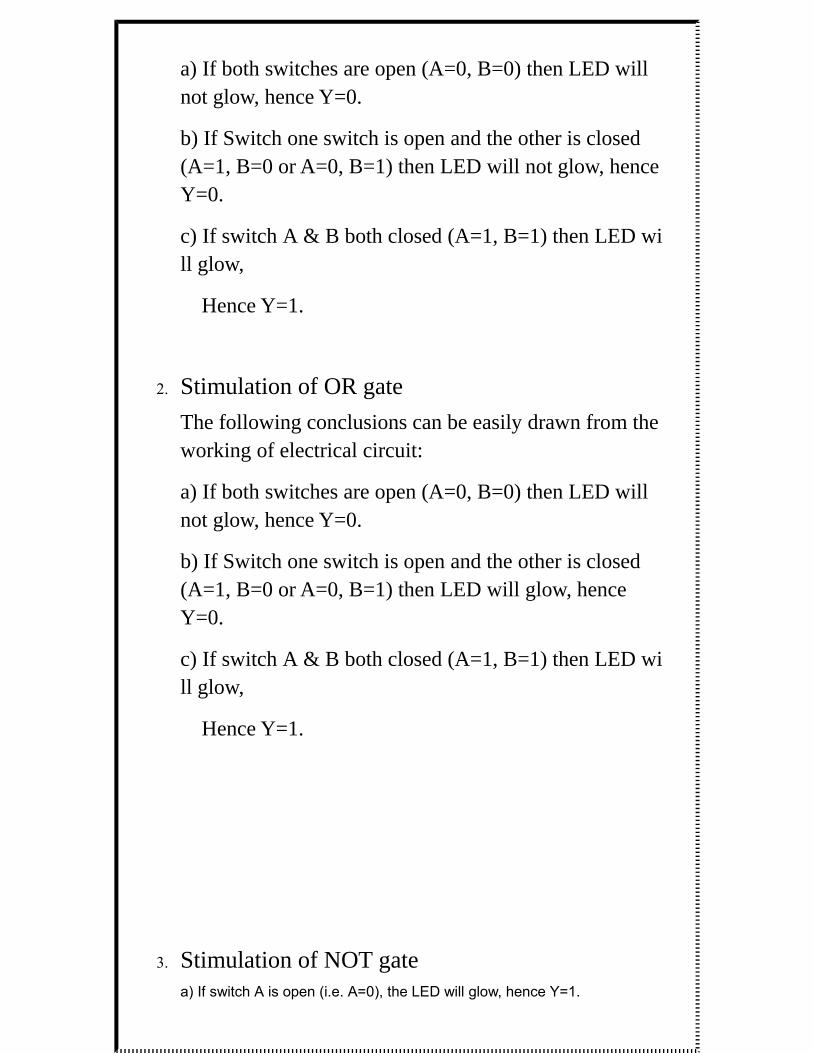
a) If both switches are open (A=0, B=0) then LED will not glow, hence Y=0.
b) If Switch one switch is open and the other is closed (A=1, B=0 or A=0, B=1) then LED will not glow, hence Y=0.
c) If switch A & B both closed (A=1, B=1) then LED will glow,
Hence Y=1.
2. Stimulation of OR gate
The following conclusions can be easily drawn from the working of electrical circuit:
a) If both switches are open (A=0, B=0) then LED will not glow, hence Y=0.
b) If Switch one switch is open and the other is closed (A=1, B=0 or A=0, B=1) then LED will glow, hence Y=0.
c) If switch A & B both closed (A=1, B=1) then LED will glow,
Hence Y=1.
3. Stimulation of NOT gate a) If switch A is open (i.e. A=0), the LED will glow, hence Y=1.
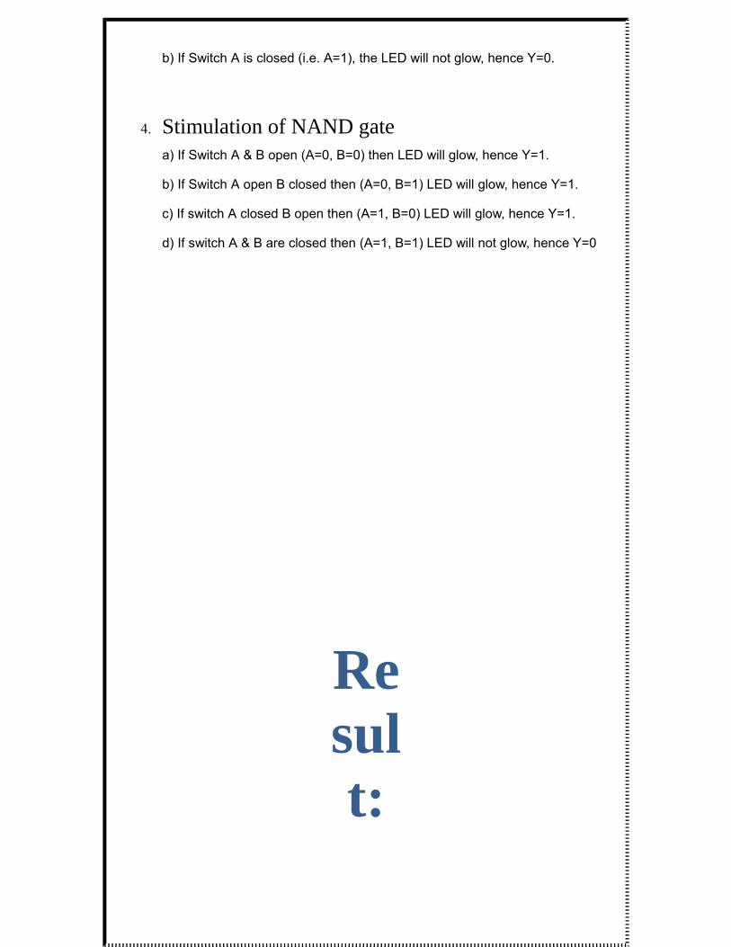
b) If Switch A is closed (i.e. A=1), the LED will not glow, hence Y=0.
4. Stimulation of NAND gate a) If Switch A & B open (A=0, B=0) then LED will glow, hence Y=1.
b) If Switch A open B closed then (A=0, B=1) LED will glow, hence Y=1.
c) If switch A closed B open then (A=1, B=0) LED will glow, hence Y=1.
d) If switch A & B are closed then (A=1, B=1) LED will not glow, hence Y=0
Result:

Basic logic gates were designed and simulated and logic circuit
was prepared for the given truth table
BIBLIOGRAPHY:-
Wikipedia
Electronic devices and circuits by J B Gupta
Conceptual physics by G C Agarwal
Encarta


![Gates and Logic: From Transistors to Logic Gates and Logic ......Gates and Logic: From Transistors to Logic Gates and Logic Circuits [Weatherspoon, Bala, Bracy, and Sirer] Prof. Hakim](https://img.dokumen.tips/doc/110x75/5fa95cb6eb1af8231472f381/gates-and-logic-from-transistors-to-logic-gates-and-logic-gates-and-logic.jpg)