Embed Size (px)
Citation preview
P H Y S I C S F O R F U T U R E T E C H N O L O G Y
Condensed matter
Foreword
Physics and physicists play a vital role in underpinningour way of life, improving its quality and contributingin a major way to wealth creation. Innovations aspowerful and diverse as the World Wide Web andmagnetic resonance imaging (MRI) have emergedfrom studies in basic physics, becoming everydaytechnologies in just two decades. It is, therefore, aworthwhile challenge to speculate where similarexplorations today will lead us in the future.
This booklet, the first in a series covering the mainareas of physics, attempts to do just that: highlight andshowcase world-class UK work that has the greatestpotential for commercial exploitation. It is jointlysponsored by the Institute of Physics – the professionalbody and learned society for physics and physicists –and the Engineering and Physical Sciences ResearchCouncil (EPSRC) – one of the largest UK funders ofphysics research.
We hope that this booklet illustrates how theresearch investment made by the EPSRC and thesupport provided by the Institute to its membership,will enable the UK’s economy, and society at large, tobenefit from the discoveries and advances in physicsbeing made.
Dr Robert Kirby-HarrisChief ExecutiveThe Institute of Physics
Dr Randal RichardsInterim Chief ExecutiveEPSRC

Foreword
Introduction
Nanoparticles in medicine
The optical, electronic and magnetic properties of minute metalparticles are being exploited to diagnose and cure disease
Wonderful carbon
One of the most mundane materials, carbon, could be the futureof nano-electronics
Quantum dots light up the future
A novel type of semiconductor nano-structure is set to becomea key element in future optoelectronic technology
A new spin on electronics
Future computer-processing elements, as well as memorydevices, could be based on the electron’s property of spin
Going with the flow
What controls how easily a molten plastic squeezes through anozzle or whether mayonnaise separates?
Keeping up with Moore’s law
Is there a limit to the number and size of devices on anelectronic chip? Industry and university research groups areexploring the possibilities
Contacts
2
4
6
8
10
12
14
16
Contents
QD QD Au
Au
AuTGCA
T-G-C-A-
-A-C-G-T
-A-C-G-T
-A-C-G-T-C-T
10x
+
QD
TGCA
-A-C-G-T
-A-C-G-T-C-T
hysics is the study of Nature at its mostfundamental level; it involves developing detailed
mathematical descriptions of how matter and energyare organised and behave – from the microscopic tothe cosmic scale. Practical applications can then bedeveloped from the insights gained.
The science of everyday materials
Condensed matter research represents one of themost important areas of physics. It covers both solidsand liquids, and the aim is to understand their bulkphysical properties in terms of the structure andbehaviour of the atomic or molecular constituents.Many of the everyday materials and consumer items on which we now depend have been developedas a result of knowledge attained through this kind of approach.
Electronic materials Condensed matter systems are often extremelycomplex. They may be solids with crystalline structuresin which the atoms or molecules are arranged in orderlyarrays, for example diamond, metals, minerals and manyorganic materials. The electrons constituting their atomsmay show a bewildering variety of behaviour such asmagnetism, electrical conductivity, semiconductivity,superconductivity and optical properties, all of whichcan be exploited technologically.
Physicists continue to uncover unusual structureswith unexpected electronic behaviour. For example, inthe past 20 years, a series of copper-oxygen ceramiccompounds were discovered to be superconducting
(conduct electricity without resistance) at temperaturesthat could be reached by cooling with liquid nitrogen.Previously, superconductivity had been seen in a fewmetals, alloys, and exotic materials but only attemperatures not much above absolute zero. Whenthe first discovery was made, it took everyone bysurprise and caused great excitement. A huge amountof research has since gone into understanding thesematerials. Even now, theorists do not have a detailedunderstanding of how higher-temperaturesuperconductivity works. Materials scientists also havebeen investigating the best way of processing theceramics into wires and other physical shapes forapplications. The work is exciting because theeconomic pay-off is potentially enormous, offering theprospect of cheaper, greener, more efficient powertransmission, travel and communications.
Many of the materials with unusual electronicproperties result from manipulating their crystalstructures in some way, such as replacing or removingsingle atoms to create what are called defects. Thesemiconductor devices – memories and processors –found in computers and mobile phones have evolvedfrom a profound understanding of the underlyingphysics of such structures.
Glasses and plasticsOther materials have a completely disorderly structure,forming solid ‘glasses’ or liquids. Understanding how aglass melts into a liquid may be important indetermining its robustness and usefulness, or methodof manufacture. Polymers such as polythene consist of
I N T R O D U C T I O N
P
R E S E A R C H I N T O C O N D E N S E D
M AT T E R U N D E R P I N S M U C H O F T H E
T E C H N O L O G Y W E U S E T O D AY
What is condensed matter physics
2
long chains of carbon atoms arranged randomly,making the material soft and flexible, but they can alsohave regions of crystallinity which impart hardness.Being able to control the arrangements of the chains,and how they move when they start to melt, isessential in the industrial processing of plastics.
Complex fluidsA field of growing commercial and medicalimportance involves liquid or gel-like materials calledcolloids containing many different kinds of moleculeswhich may be self-organised into minute particleswith a complex structure tailored to produce requiredphysical and chemical properties. The averagewashing-up liquid, paint or cosmetic is extremelysophisticated in design, to give the characteristics theconsumer wants.
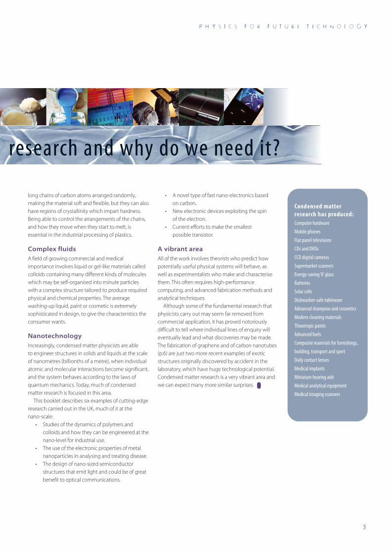
Nanotechnology Increasingly, condensed matter physicists are able to engineer structures in solids and liquids at the scaleof nanometres (billionths of a metre), when individualatomic and molecular interactions become significant,and the system behaves according to the laws ofquantum mechanics. Today, much of condensedmatter research is focused in this area.
This booklet describes six examples of cutting-edgeresearch carried out in the UK, much of it at the nano-scale:
• Studies of the dynamics of polymers andcolloids and how they can be engineered at thenano-level for industrial use.
• The use of the electronic properties of metalnanoparticles in analysing and treating disease.
• The design of nano-sized semiconductorstructures that emit light and could be of greatbenefit to optical communications.
• A novel type of fast nano-electronics based on carbon.
• New electronic devices exploiting the spin of the electron.
• Current efforts to make the smallest possible transistor.
A vibrant areaAll of the work involves theorists who predict howpotentially useful physical systems will behave, as well as experimentalists who make and characterisethem. This often requires high-performancecomputing, and advanced fabrication methods andanalytical techniques.
Although some of the fundamental research thatphysicists carry out may seem far removed fromcommercial application, it has proved notoriouslydifficult to tell where individual lines of enquiry willeventually lead and what discoveries may be made.The fabrication of graphene and of carbon nanotubes(p.6) are just two more recent examples of exoticstructures originally discovered by accident in thelaboratory, which have huge technological potential.Condensed matter research is a very vibrant area andwe can expect many more similar surprises.
P H Y S I C S F O R F U T U R E T E C H N O L O G Y
research and why do we need it?
3
Condensed matter research has produced:Computer hardware
Mobile phones
Flat panel televisions
CDs and DVDs
CCD digital cameras
Supermarket scanners
Energy-saving ‘K’ glass
Batteries
Solar cells
Dishwasher-safe tableware
Advanced shampoos and cosmetics
Modern cleaning materials
Thixotropic paints
Advanced fuels
Composite materials for furnishings,
building, transport and sport
Daily contact lenses
Medical implants
Miniature hearing aids
Medical analytical equipment
Medical imaging scanners
n important characteristic of particles just a fewnanometres across is that they are of the right scale
to interact with biological molecules and living cells ina specific and guided manner. Metal nanoparticles, in particular, possess physical characteristics that makethem ideal diagnostic probes or even therapeuticagents. A number of UK research groups are focusing ondeveloping novel strategies involving gold, silver andmagnetic nanoparticles to aid the treatment of disease.
Gold and silver owe their colour and shininess tooscillations of free electrons on their surface calledplasmons which control how light is reflected. Theplasmon frequency is also affected by the size andshape of the metal surface. Consequently goldnanoparticles are deep red but change to blue whenthe particles cluster into larger objects; for silverparticles the colour change is from yellow to orange.David Russell at the University of East Anglia has beenexploiting this effect to develop a test for detectingbacterial toxins such as cholera toxin. Goldnanoparticles are attached to carbohydrate moleculesdesigned to recognise the toxin. When thecarbohydrate binds to the toxin, the gold particlesaggregate and the colour changes.
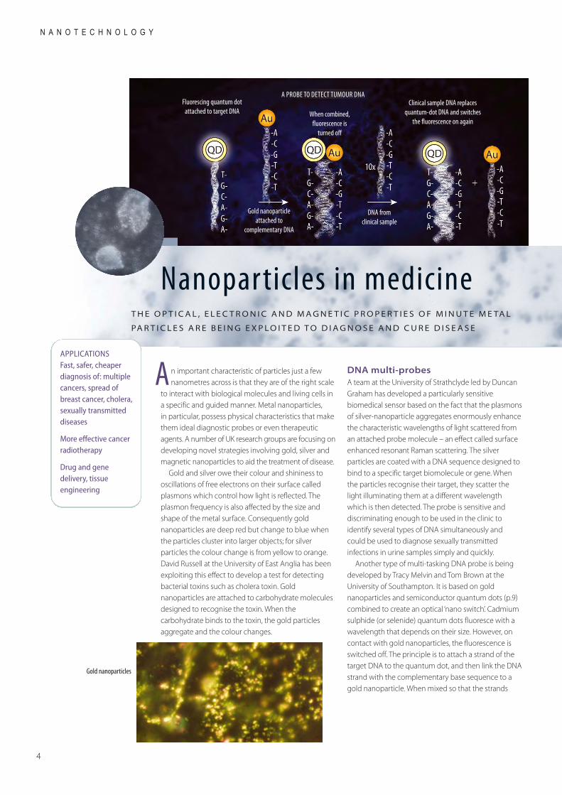
DNA multi-probesA team at the University of Strathclyde led by DuncanGraham has developed a particularly sensitivebiomedical sensor based on the fact that the plasmonsof silver-nanoparticle aggregates enormously enhancethe characteristic wavelengths of light scattered froman attached probe molecule – an effect called surfaceenhanced resonant Raman scattering. The silverparticles are coated with a DNA sequence designed tobind to a specific target biomolecule or gene. Whenthe particles recognise their target, they scatter thelight illuminating them at a different wavelengthwhich is then detected. The probe is sensitive anddiscriminating enough to be used in the clinic toidentify several types of DNA simultaneously andcould be used to diagnose sexually transmittedinfections in urine samples simply and quickly.
Another type of multi-tasking DNA probe is beingdeveloped by Tracy Melvin and Tom Brown at theUniversity of Southampton. It is based on goldnanoparticles and semiconductor quantum dots (p.9)combined to create an optical ‘nano switch’. Cadmiumsulphide (or selenide) quantum dots fluoresce with awavelength that depends on their size. However, oncontact with gold nanoparticles, the fluorescence isswitched off. The principle is to attach a strand of thetarget DNA to the quantum dot, and then link the DNAstrand with the complementary base sequence to agold nanoparticle. When mixed so that the strands
T H E O P T I C A L , E L E C T R O N I C A N D M A G N E T I C P R O P E R T I E S O F M I N U T E M E TA L
PA R T I C L E S A R E B E I N G E X P L O I T E D T O D I A G N O S E A N D C U R E D I S E A S E
N A N O T E C H N O L O G Y
A
Nanoparticles in medicine
4
Fluorescing quantum dotattached to target DNA
Clinical sample DNA replacesquantum-dot DNA and switches
the fluorescence on againWhen combined,
fluorescence isturned off
DNA fromclinical sample
Gold nanoparticleattached to
complementary DNA
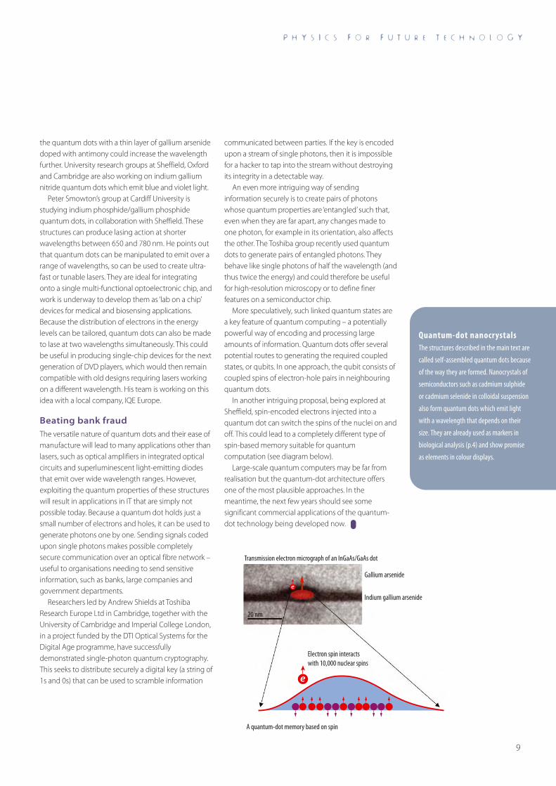
A PROBE TO DETECT TUMOUR DNA
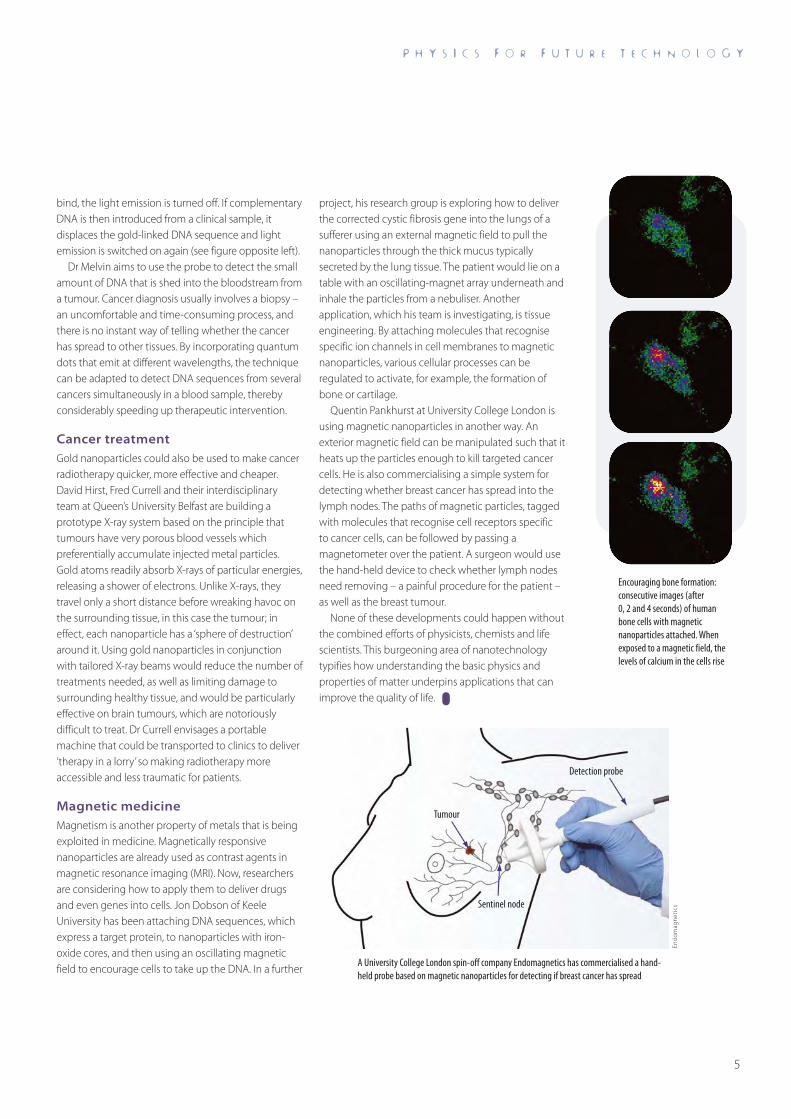
Gold nanoparticles
APPLICATIONSFast, safer, cheaperdiagnosis of: multiplecancers, spread ofbreast cancer, cholera,sexually transmitteddiseases
More effective cancerradiotherapy
Drug and genedelivery, tissueengineering
bind, the light emission is turned off. If complementaryDNA is then introduced from a clinical sample, itdisplaces the gold-linked DNA sequence and lightemission is switched on again (see figure opposite left).
Dr Melvin aims to use the probe to detect the smallamount of DNA that is shed into the bloodstream froma tumour. Cancer diagnosis usually involves a biopsy –an uncomfortable and time-consuming process, andthere is no instant way of telling whether the cancerhas spread to other tissues. By incorporating quantumdots that emit at different wavelengths, the techniquecan be adapted to detect DNA sequences from severalcancers simultaneously in a blood sample, therebyconsiderably speeding up therapeutic intervention.
Cancer treatmentGold nanoparticles could also be used to make cancerradiotherapy quicker, more effective and cheaper.David Hirst, Fred Currell and their interdisciplinaryteam at Queen’s University Belfast are building aprototype X-ray system based on the principle thattumours have very porous blood vessels whichpreferentially accumulate injected metal particles.Gold atoms readily absorb X-rays of particular energies,releasing a shower of electrons. Unlike X-rays, theytravel only a short distance before wreaking havoc onthe surrounding tissue, in this case the tumour; ineffect, each nanoparticle has a ‘sphere of destruction’around it. Using gold nanoparticles in conjunctionwith tailored X-ray beams would reduce the number oftreatments needed, as well as limiting damage tosurrounding healthy tissue, and would be particularlyeffective on brain tumours, which are notoriouslydifficult to treat. Dr Currell envisages a portablemachine that could be transported to clinics to deliver‘therapy in a lorry’ so making radiotherapy moreaccessible and less traumatic for patients.
Magnetic medicineMagnetism is another property of metals that is beingexploited in medicine. Magnetically responsivenanoparticles are already used as contrast agents inmagnetic resonance imaging (MRI). Now, researchersare considering how to apply them to deliver drugsand even genes into cells. Jon Dobson of KeeleUniversity has been attaching DNA sequences, whichexpress a target protein, to nanoparticles with iron-oxide cores, and then using an oscillating magneticfield to encourage cells to take up the DNA. In a further
project, his research group is exploring how to deliverthe corrected cystic fibrosis gene into the lungs of asufferer using an external magnetic field to pull thenanoparticles through the thick mucus typicallysecreted by the lung tissue. The patient would lie on atable with an oscillating-magnet array underneath andinhale the particles from a nebuliser. Anotherapplication, which his team is investigating, is tissueengineering. By attaching molecules that recognisespecific ion channels in cell membranes to magneticnanoparticles, various cellular processes can beregulated to activate, for example, the formation ofbone or cartilage.
Quentin Pankhurst at University College London isusing magnetic nanoparticles in another way. Anexterior magnetic field can be manipulated such that itheats up the particles enough to kill targeted cancercells. He is also commercialising a simple system fordetecting whether breast cancer has spread into thelymph nodes. The paths of magnetic particles, taggedwith molecules that recognise cell receptors specific to cancer cells, can be followed by passing amagnetometer over the patient. A surgeon would usethe hand-held device to check whether lymph nodesneed removing – a painful procedure for the patient –as well as the breast tumour.
None of these developments could happen withoutthe combined efforts of physicists, chemists and lifescientists. This burgeoning area of nanotechnologytypifies how understanding the basic physics andproperties of matter underpins applications that canimprove the quality of life.
P H Y S I C S F O R F U T U R E T E C H N O L O G Y
Encouraging bone formation:consecutive images (after 0, 2 and 4 seconds) of humanbone cells with magneticnanoparticles attached. Whenexposed to a magnetic field, thelevels of calcium in the cells rise
A University College London spin-off company Endomagnetics has commercialised a hand-held probe based on magnetic nanoparticles for detecting if breast cancer has spread
5
Endo
mag
neti
cs
Tumour
Detection probe
Sentinel node
arbon is the most chemically versatile of all theelements and is, of course, the basis of life. It exists
in many forms – the two most well-known beingdiamond, a three-dimensional network of single bonds;and graphite, a two-dimensional hexagonal network ofelectron-rich double bonds arranged in layers. Graphiteis the most common and most stable form, and foundin coal and soot. Despite the fact that it is known toconduct electricity along the layers, it is only recentlythat graphite’s potential as an electronic material hascome to the fore. Recent research has uncovered thatthe basic chicken-wire network – graphene – can existin architectures with a rich and surprising array ofproperties that could lead to a new generation ofcarbon-based electronic and photonic devices.
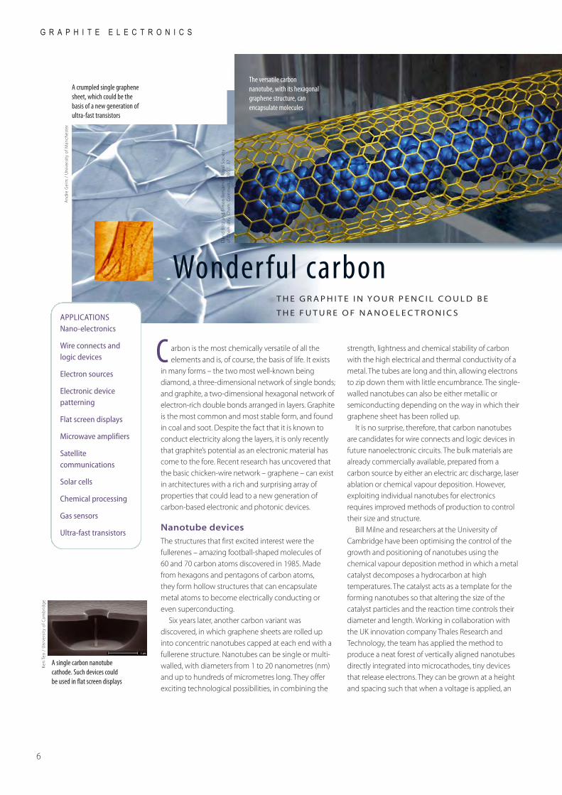
Nanotube devicesThe structures that first excited interest were thefullerenes – amazing football-shaped molecules of 60 and 70 carbon atoms discovered in 1985. Madefrom hexagons and pentagons of carbon atoms, they form hollow structures that can encapsulatemetal atoms to become electrically conducting oreven superconducting.
Six years later, another carbon variant wasdiscovered, in which graphene sheets are rolled upinto concentric nanotubes capped at each end with afullerene structure. Nanotubes can be single or multi-walled, with diameters from 1 to 20 nanometres (nm)and up to hundreds of micrometres long. They offerexciting technological possibilities, in combining the
strength, lightness and chemical stability of carbonwith the high electrical and thermal conductivity of ametal. The tubes are long and thin, allowing electronsto zip down them with little encumbrance. The single-walled nanotubes can also be either metallic orsemiconducting depending on the way in which theirgraphene sheet has been rolled up.
It is no surprise, therefore, that carbon nanotubesare candidates for wire connects and logic devices infuture nanoelectronic circuits. The bulk materials arealready commercially available, prepared from acarbon source by either an electric arc discharge, laserablation or chemical vapour deposition. However,exploiting individual nanotubes for electronicsrequires improved methods of production to controltheir size and structure.
Bill Milne and researchers at the University ofCambridge have been optimising the control of thegrowth and positioning of nanotubes using thechemical vapour deposition method in which a metalcatalyst decomposes a hydrocarbon at hightemperatures. The catalyst acts as a template for theforming nanotubes so that altering the size of thecatalyst particles and the reaction time controls theirdiameter and length. Working in collaboration with the UK innovation company Thales Research andTechnology, the team has applied the method toproduce a neat forest of vertically aligned nanotubesdirectly integrated into microcathodes, tiny devicesthat release electrons. They can be grown at a heightand spacing such that when a voltage is applied, an
G R A P H I T E E L E C T R O N I C S
C
A single carbon nanotubecathode. Such devices couldbe used in flat screen displays
T H E G R A P H I T E I N Y O U R P E N C I L C O U L D B E
T H E F U T U R E O F N A N O E L E C T R O N I C S
Wonderful carbon
6
The versatile carbonnanotube, with its hexagonalgraphene structure, canencapsulate molecules
A crumpled single graphenesheet, which could be thebasis of a new generation ofultra-fast transistors
Dav
id B
ritz
and
Sim
on B
enja
min
/ Ro
yal S
ocie
tyof
Che
mis
try,
Che
m. C
omm
un.,
2005
,1, 3
7
And
re G
eim
/ U
nive
rsit
y of
Man
ches
ter
Ken
Teo
/ U
nive
rsit
y of
Cam
bri
dge
APPLICATIONSNano-electronics
Wire connects andlogic devices
Electron sources
Electronic devicepatterning
Flat screen displays
Microwave amplifiers
Satellitecommunications
Solar cells
Chemical processing
Gas sensors
Ultra-fast transistors
intense stream of electrons is emitted. The ‘forest’ canbe used in field-emission displays (flat screens in whichan array of minute cathode-ray tubes provide thedisplay elements), and the emission from an individualnanotube can be applied in an electron microscope.Because of the huge current-carrying capacity ofnanotubes, such cold-cathode electron sources promiseto be much more efficient than current systems relyingon thermionic emission. One immediate applicationthat the team is working on is a small, lightweightmicrowave amplifier for satellite communications.
The semiconducting nanotubes have energy levelscomparable to those in silicon and gallium arsenide,and could be employed in optical applicationsincluding sensors and photovoltaic cells. RobinNicholas’s group at the University of Oxford has beenstudying how to achieve this by looking at the way theemission and absorption of light is affected by thenanotubes’ chemical and physical environment. Aswell as external factors such as magnetic fields, strain,temperature and pressure, the properties of the tubescan also be controlled by inserting molecules insidethem. Oxford researcher David Britz and colleagueshave even managed to perform chemical reactionsinside nanotubes, taking them into the Guinness Bookof World Records by making the world’s smallest test-tube (main image, opposite page). They insertedfullerene molecules to form a ‘peapod’ structure andthen showed that the fullerenes would polymerise toform a long chain only when inside a nanotube.
Ultrafast transistorsWhile some physicists have been exploring thepotential of nanotubes, others have been studying thefundamental two-dimensional building material forgraphite and nanotubes – graphene. Although long-studied as a theoretical model and used to explainproperties of other graphitic materials, graphene itselfwas thought to be too unstable to exist. However,three years ago, physicists at the University ofManchester led by Andre Geim made free graphenefor the first time in a surprisingly simple way. They usedan adhesive tape to peel off a one-atom-thick layerfrom a graphite surface – the equivalent of drawingwith a graphite pencil.
The graphene crystals obtained were good enoughto reveal some bizarre behaviour, which has got theattention of both theorists and experimentalists,rapidly becoming one of the hottest research topics in
physics. The unusual quantum characteristics ofgraphene’s electronic structure result in theconducting electrons behaving like massless particles(like photons with an electric charge). The electronmobility is thus enormous and offers a real possibilityof making ultra-fast transistors based on the motion of individual electrons without scattering (ballisticelectrons). Graphene may also find use in spintronics(p.10), in field-emitting devices, and as gas sensorssince it absorbs gas molecules which then alter itsresistivity. Researchers are already looking at thefeasibility of patterning electron microprocessors on asingle graphene sheet. This is a brand new field ofresearch and we can expect many excitingdevelopments in the next few years.
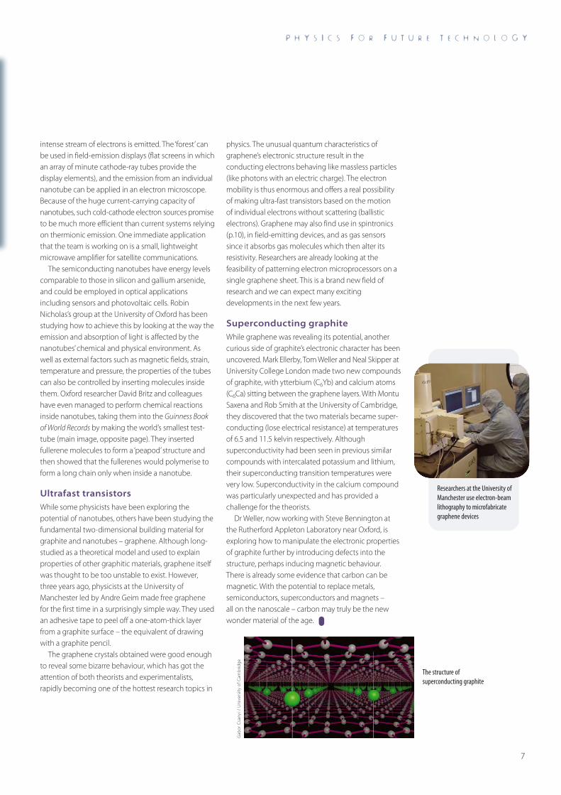
Superconducting graphiteWhile graphene was revealing its potential, anothercurious side of graphite’s electronic character has beenuncovered. Mark Ellerby, Tom Weller and Neal Skipper atUniversity College London made two new compoundsof graphite, with ytterbium (C6Yb) and calcium atoms(C6Ca) sitting between the graphene layers. With MontuSaxena and Rob Smith at the University of Cambridge,they discovered that the two materials became super-conducting (lose electrical resistance) at temperaturesof 6.5 and 11.5 kelvin respectively. Althoughsuperconductivity had been seen in previous similarcompounds with intercalated potassium and lithium,their superconducting transition temperatures werevery low. Superconductivity in the calcium compoundwas particularly unexpected and has provided achallenge for the theorists.
Dr Weller, now working with Steve Bennington atthe Rutherford Appleton Laboratory near Oxford, isexploring how to manipulate the electronic propertiesof graphite further by introducing defects into thestructure, perhaps inducing magnetic behaviour. There is already some evidence that carbon can bemagnetic. With the potential to replace metals,semiconductors, superconductors and magnets – all on the nanoscale – carbon may truly be the newwonder material of the age.
P H Y S I C S F O R F U T U R E T E C H N O L O G Y
Researchers at the University ofManchester use electron-beamlithography to microfabricategraphene devices
The structure ofsuperconducting graphite
7
Gab
or C
sany
i / U
nive
rsit
y of
Cam
bri
dge
n the past 20 years, semiconductor lasershave become ubiquitous. They are found in
supermarket scanners, CD players andcomputer printers. The field is still moving fast – recentdevelopments are the result of a reduction in the sizeand dimensionality of the light-emitting device. Thenext generation of lasers will be based on minutesemiconductor structures called quantum dots.
Quantum dots are typically only 10 to 50 nm acrossand contain just a few hundred or thousand atoms.They are designed to confine the movements of theelectrons responsible for semiconducting activitywithin the dot. The result is an object with electronstrapped in discrete quantised energy levels, as in anatom. These electrons can be excited into higherenergy states, at the same time leaving behind apositively charged ‘hole’. Recombination of the electron-hole pairs results in the emission of light whosewavelength depends on the size, shape and
configuration of the dots.Quantum dots form when a very thin
film of one semiconductor is fabricatedon the surface of another with a slightlydifferent crystal-lattice size, for example,indium arsenide grown on a substrateof gallium arsenide (InAs/GaAs). Themismatch creates stresses which causethe film to buckle and form tiny three-dimensional blobs. Further layers of thesemiconductors can be grown on top tobuild up a lasing device comprisingseveral layers of millions of dots.
Lasers for optical communicationsQuantum-dot lasers are more stable and use lesspower than the current generation of so-calledquantum-well lasers (in which the electrons areconfined in two-dimensional layers); they can also bemade cheaply (an important consideration for theconsumer electronics market) and the frequencyoutput is more stable. They are also less affected bytemperature. This is an advantage in one potential use:in optical communications, which may be subject to avariety of environments. This application relies on laserpulses operating at 1300 and 1500 nm – thewavelengths at which light dispersion and attenuationrespectively are minimised in optical fibres. Researchgroups both in industry and academia are striving toattain these wavelengths with quantum dots, and1300-nm quantum-dot lasers are just starting tobecome commercially available.
The quantum-well lasers currently used to couplelight into optical fibres are based on indium phosphide(InP), but teams involving Ray Murray at ImperialCollege London and Maurice Skolnick at the Universityof Sheffield are working with InAs/GaAs quantum dotswhich have the advantage of being easily integratedonto the same gallium arsenide chips as the electricaldrive circuits. By manipulating the size andcomposition of the dot, the researchers havedemonstrated lasing at 1520 nm in different quantum-dot systems. According to Professor Skolnick, covering
Q U A N T U M E L E C T R O N I C S
I
A N O V E L T Y P E O F S E M I C O N D U C T O R
N A N O S T R U C T U R E I S S E T T O
B E C O M E A K E Y E L E M E N T I N
O P T O E L E C T R O N I C T E C H N O L O G Y
Quantum dots light up the future
8
UK researchers at Toshiba andthe University of Cambridgedemonstrate quantumcryptography, which couldhelp keep bank accountscompletely secure
An atomic force micrograph showing alayer of quantum-dot structures
Imperial College London
APPLICATIONSUltra-fast, tunablelasers
More efficient opticalcommunications
DVD players
Security andencryption
High-resolutionmicroscopy
Chip fabrication
Quantum computing
the quantum dots with a thin layer of gallium arsenidedoped with antimony could increase the wavelengthfurther. University research groups at Sheffield, Oxfordand Cambridge are also working on indium galliumnitride quantum dots which emit blue and violet light.
Peter Smowton’s group at Cardiff University isstudying indium phosphide/gallium phosphidequantum dots, in collaboration with Sheffield. Thesestructures can produce lasing action at shorterwavelengths between 650 and 780 nm. He points outthat quantum dots can be manipulated to emit over arange of wavelengths, so can be used to create ultra-fast or tunable lasers. They are ideal for integratingonto a single multi-functional optoelectronic chip, andwork is underway to develop them as ‘lab on a chip’devices for medical and biosensing applications.Because the distribution of electrons in the energylevels can be tailored, quantum dots can also be madeto lase at two wavelengths simultaneously. This couldbe useful in producing single-chip devices for the nextgeneration of DVD players, which would then remaincompatible with old designs requiring lasers workingon a different wavelength. His team is working on thisidea with a local company, IQE Europe.
Beating bank fraudThe versatile nature of quantum dots and their ease ofmanufacture will lead to many applications other thanlasers, such as optical amplifiers in integrated opticalcircuits and superluminescent light-emitting diodesthat emit over wide wavelength ranges. However,exploiting the quantum properties of these structureswill result in applications in IT that are simply notpossible today. Because a quantum dot holds just asmall number of electrons and holes, it can be used togenerate photons one by one. Sending signals codedupon single photons makes possible completelysecure communication over an optical fibre network –useful to organisations needing to send sensitiveinformation, such as banks, large companies andgovernment departments.
Researchers led by Andrew Shields at ToshibaResearch Europe Ltd in Cambridge, together with theUniversity of Cambridge and Imperial College London,in a project funded by the DTI Optical Systems for theDigital Age programme, have successfullydemonstrated single-photon quantum cryptography.This seeks to distribute securely a digital key (a string of1s and 0s) that can be used to scramble information
communicated between parties. If the key is encodedupon a stream of single photons, then it is impossiblefor a hacker to tap into the stream without destroyingits integrity in a detectable way.
An even more intriguing way of sendinginformation securely is to create pairs of photonswhose quantum properties are ‘entangled’ such that,even when they are far apart, any changes made toone photon, for example in its orientation, also affectsthe other. The Toshiba group recently used quantumdots to generate pairs of entangled photons. Theybehave like single photons of half the wavelength (andthus twice the energy) and could therefore be usefulfor high-resolution microscopy or to define finerfeatures on a semiconductor chip.
More speculatively, such linked quantum states area key feature of quantum computing – a potentiallypowerful way of encoding and processing largeamounts of information. Quantum dots offer severalpotential routes to generating the required coupledstates, or qubits. In one approach, the qubit consists ofcoupled spins of electron-hole pairs in neighbouringquantum dots.
In another intriguing proposal, being explored atSheffield, spin-encoded electrons injected into aquantum dot can switch the spins of the nuclei on andoff. This could lead to a completely different type ofspin-based memory suitable for quantumcomputation (see diagram below).
Large-scale quantum computers may be far fromrealisation but the quantum-dot architecture offersone of the most plausible approaches. In themeantime, the next few years should see somesignificant commercial applications of the quantum-dot technology being developed now.
P H Y S I C S F O R F U T U R E T E C H N O L O G Y
9
Quantum-dot nanocrystalsThe structures described in the main text are
called self-assembled quantum dots because
of the way they are formed. Nanocrystals of
semiconductors such as cadmium sulphide
or cadmium selenide in colloidal suspension
also form quantum dots which emit light
with a wavelength that depends on their
size. They are already used as markers in
biological analysis (p.4) and show promise
as elements in colour displays.
Indium gallium arsenide
Gallium arsenide
Transmission electron micrograph of an InGaAs/GaAs dot
A quantum-dot memory based on spin
Electron spin interactswith 10,000 nuclear spins
20 nm
he past 10 years has seen a revolution in electronicstorage capacity. The latest devices such as the iPod
rely on magnetic technology that can store 100 milliontimes more data than was possible on a computerhard disk of 50 years ago.
Memory devices rely on recording and storing dataas magnetised domains in metallic films. Themagnetism is the result of the electrons in the materialhaving a quantum property called spin which can beoriented ‘up’ or ‘down’. As the disk turns, a read-headabove detects the minute magnetic field changesresulting from the two possible magnetic orientationsof the domains. This produces correspondingvariations in the head’s electrical resistance – an effectcalled magnetoresistance.
In 1997 IBM introduced a new type of read-headbased on another effect, discovered only a few yearsbefore, called ‘giant magnetoresistance’ (GMR); withGMR, the change in electrical resistance is 10 times asgreat. GMR is seen in ultra-thin layers of magneticmaterials such as cobalt interleaved with a layer of anonmagnetic metal such as copper. A current passingthrough the layers consists of spin-up and spin-downelectrons, and those that are aligned with the electronspins in a magnetic layer pass through much moreeasily than those aligned in the opposite direction.When the spin orientations in the layers are the same,more electrons pass through than when they areoppositely aligned. If the alignment in one layer isaltered by a nearby magnetic field, the resistancechanges quite dramatically. Today, all computer disksare based on very sensitive spin-filter devices that work on this principle.
More powerful computer memoriesPhysicists are now exploring other ways ofmanipulating electron spins to create a newgeneration of ‘spintronic’ memory and circuit elements.They promise to be smaller, more robust and moreversatile than the current generation. The firstapplication has been to devise magnetic randomaccess memory (MRAM) chips, which have theadvantage of being ‘non-volatile’ – information is notlost when the computer is switched off. MRAM chipsstarted to be manufactured in 2004 and further designimprovements are continuing apace.
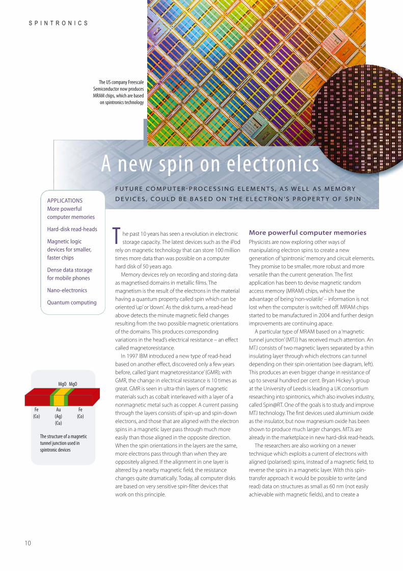
A particular type of MRAM based on a ‘magnetictunnel junction’ (MTJ) has received much attention. AnMTJ consists of two magnetic layers separated by a thininsulating layer through which electrons can tunneldepending on their spin orientation (see diagram, left).This produces an even bigger change in resistance ofup to several hundred per cent. Bryan Hickey’s groupat the University of Leeds is leading a UK consortiumresearching into spintronics, which also involves industry,called Spin@RT. One of the goals is to study and improveMTJ technology. The first devices used aluminium oxideas the insulator, but now magnesium oxide has beenshown to produce much larger changes. MTJs arealready in the marketplace in new hard-disk read-heads.
The researchers are also working on a newertechnique which exploits a current of electrons withaligned (polarised) spins, instead of a magnetic field, toreverse the spins in a magnetic layer. With this spin-transfer approach it would be possible to write (andread) data on structures as small as 60 nm (not easilyachievable with magnetic fields), and to create a
S P I N T R O N I C S
T
F U T U R E C O M P U T E R P R O C E S S I N G E L E M E N T S , A S W E L L A S M E M O R Y
D E V I C E S , C O U L D B E B A S E D O N T H E E L E C T R O N ’ S P R O P E R T Y O F S P I N
A new spin on electronics
10
MgO MgO
Au(Ag)(Cu)
Fe(Co)
Fe(Co)
The structure of a magnetictunnel junction used inspintronic devices
The US company FreescaleSemiconductor now producesMRAM chips, which are based
on spintronics technology
APPLICATIONSMore powerfulcomputer memories
Hard-disk read-heads
Magnetic logicdevices for smaller,faster chips
Dense data storagefor mobile phones
Nano-electronics
Quantum computing
spintronic-based switching device.The possibility of manipulating spins with an
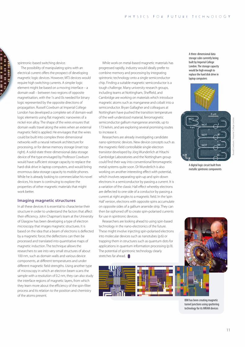
electrical current offers the prospect of developingmagnetic logic devices. However, MTJ devices wouldrequire high switching currents. A simpler logicelement might be based on a moving interface – adomain wall – between two regions of oppositemagnetisation, with the 1s and 0s needed for binarylogic represented by the opposite directions ofpropagation. Russell Cowburn at Imperial CollegeLondon has developed a complete set of domain-walllogic elements using flat magnetic nanowires of anickel-iron alloy. The shape of the wires ensures thatdomain walls travel along the wires when an externalmagnetic field is applied. He envisages that the wirescould be built into complex three-dimensionalnetworks with a neural network architecture forprocessing, or for dense memory storage (inset topright). A solid-state three-dimensional data storagedevice of the type envisaged by Professor Cowburnwould have sufficient storage capacity to replace thehard-disk drive in laptop computers, and would bringenormous data-storage capacity to mobile phones.While he is already looking to commercialise his noveldevices, his team is continuing to explore theproperties of other magnetic materials that mightwork better.
Imaging magnetic structuresIn all these devices it is essential to characterise theirstructure in order to understand the factors that affecttheir efficiency. John Chapman’s team at the Universityof Glasgow has been developing a type of electronmicroscopy that images magnetic structures. It isbased on the idea that a beam of electrons is deflectedby a magnetic force; the deflections can then beprocessed and translated into quantitative maps ofmagnetic induction. The technique allows theresearchers to see into very small structures of about100 nm, such as domain walls and various devicecomponents, at different temperatures and underdifferent magnetic field strengths. Using another typeof microscopy in which an electron beam scans thesample with a resolution of 0.2 nm, they can also studythe interface regions of magnetic layers, from whichthey learn more about the efficiency of the spin-filterprocess and its relation to the position and chemistryof the atoms present.
While work on metal-based magnetic materials hasprogressed rapidly, industry would ideally prefer tocombine memory and processing by integratingspintronic technology onto a single semiconductorchip. Finding a suitable magnetic semiconductor is atough challenge. Many university research groups,including teams at Nottingham, Sheffield, andCambridge are working on materials which introducemagnetic atoms such as manganese and cobalt into asemiconductor. Bryan Gallagher and colleagues atNottingham have pushed the transition temperatureof the well-understood material, ferromagneticsemiconductor gallium manganese arsenide, up to 173 kelvin, and are exploring several promising routesto increase it.
Researchers are already investigating candidatenano-spintronic devices. New device concepts such asthe magnetic-field controllable single-electrontransistor developed by Jörg Wunderlich at HitachiCambridge Laboratories and the Nottingham groupcould find their way into conventional ferromagneticmetal systems quite soon. Dr Wunderlich is alsoworking on another interesting effect with potential,which involves separating spin-up and spin-downelectrons in a semiconductor by passing a current. It isa variation of the classic Hall effect whereby electronsare deflected to one side of a conductor by passing acurrent at right angles to a magnetic field. In the ‘spinHall’ version, electrons with opposite spins accumulateon opposite sides of a gallium arsenide strip. They canthen be siphoned off to create spin-polarised currentsfor use in spintronic devices.
Researchers are looking ahead to using spin-basedtechnology in the nano-electronics of the future. These might involve injecting spin-polarised electronsinto molecular devices such as nanotubes (p.6) ortrapping them in structures such as quantum dots forapplications in quantum information processing (p.9).The potential of spintronic technology clearly stretches far ahead.
P H Y S I C S F O R F U T U R E T E C H N O L O G Y
IBM has been creating magnetictunnel junctions using sputteringtechnology for its MRAM devices
11
A digital logic circuit built frommetallic spintronic components
Russ
ell C
owb
urn
/ Im
per
ial C
olle
ge L
ondo
n
A three-dimensional datastorage cube currently beingbuilt by Imperial CollegeLondon. The storage capacitywould be high enough toreplace the hard disk drive inlaptop computers
ver the past decade or so, understanding themotion of everyday materials such as polymers and
emulsions has become an increasingly important fieldof study. The aim is to link the structural properties ofso-called ‘soft matter’ at the microscopic level to itsdynamic behaviour in a predictable way. The theoriesdeveloped can then help industry to make materialssuch as polymers and emulsions more efficiently, aswell as to design novel structures for specific uses.
Soft matter comprises a wide range of familiarmaterials – from plastics to the gels and thick liquidsassociated with foods, cleaning materials, paints andcosmetics. Biological structures such as cell walls arealso complex forms of soft matter. They all have one
thing in common: their basic components –which may be clusters of atoms, very largemolecules or complex molecular assemblies –form structures on a scale of 10 to 100 nm,which are held together by quite weak forces.This means that under everyday conditions theyare very sensitive to increased pressure, shearforces and to small changes in temperature.
Understanding plastics Amongst the most studied forms of soft matter arepolymers. These are long-chain molecules, which maybe randomly arranged and entangled, or crystallisedinto more ordered arrays. On heating, the chainsbecome more mobile, and the material becomes
softer (hence the name plastic) – eventually melting.Understanding exactly how the chains move –whether they stretch out or become more entangled –is particularly important in their industrial processing,as it affects properties like viscosity, and therefore therate at which the material flows. These characteristicsalso determine the final structure, and thus thestrength, of the solidified product.
The basic theory of polymer dynamics wasdeveloped more than 30 years ago by the UK physicistSam Edwards, together with fellow Nobel LaureatesPierre-Gilles de Gennes and Masao Doi. They imaginedeach polymer chain as snaking through a tube createdby the spatial confinement imposed by neighbouringchains. Other processes are also involved: the free endsof the chains can flip back into the tube; and understrong flow conditions, parts of the tube may rapidlyreconfigure as neighbouring tangles of chains move inand out of the way.
The bulk movement of a melted polymer is deeplyinfluenced by its composition and structure – therange of chain lengths in the melt, and the degree andtype of chain branching. For instance, although thestrength of polythene is improved by keeping all thechains the same length, the resulting unstable flowproperties mean that it processes poorly. Introducing afew branched chains makes it flow much better.
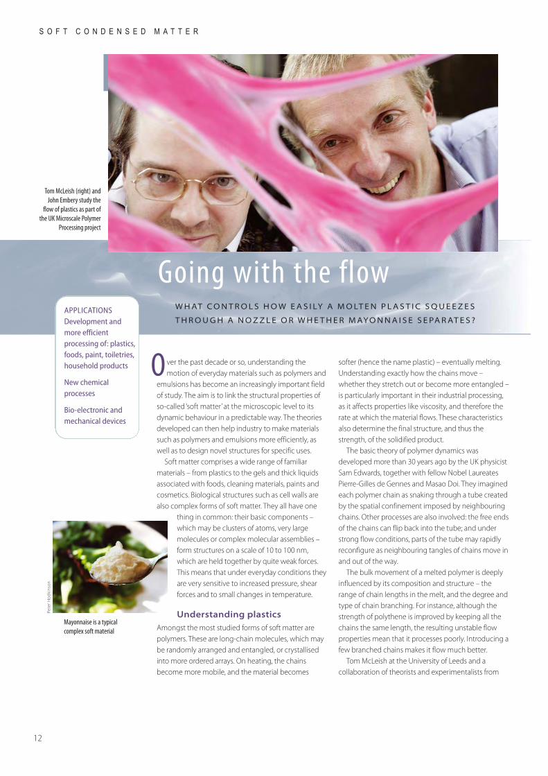
Tom McLeish at the University of Leeds and acollaboration of theorists and experimentalists from
S O F T C O N D E N S E D M A T T E R
O
W H AT C O N T R O L S H O W E A S I LY A M O LT E N P L A S T I C S Q U E E Z E S
T H R O U G H A N O Z Z L E O R W H E T H E R M AY O N N A I S E S E PA R AT E S ?
Going with the flow
12
APPLICATIONSDevelopment andmore efficientprocessing of: plastics,foods, paint, toiletries,household products
New chemicalprocesses
Bio-electronic andmechanical devices
Tom McLeish (right) andJohn Embery study the
flow of plastics as part ofthe UK Microscale Polymer
Processing project
Pete
r H
odki
nson
Mayonnaise is a typicalcomplex soft material
eight university groups have been exploring why. Theyhave extended the tube description to showtheoretically how the flipping-back behaviour of freeends in any branched chains present helps to untanglethe polymer and improve the flow. They predicted thateven H-shaped chains, which have a central cross-barwith no free ends, would disentangle in strong flowsbecause the arms of the ‘H’ can withdraw back into thetube occupied by the crossbar in a kind of breathing-inaction. The ideas were probed experimentally usingboth optical and neutron scattering (like X-raydiffraction, they can map structure at molecular scales),which identified signals from these and other subtlermolecular motions. These kinds of detailed predictionsabout the microscopic dynamic behaviour of polymersopen up the way to optimising manufacturingprocesses to match a particular product, and vice versa,in advance of expensive process-development trials atthe pilot-plant stage.
The physics of yoghurtAnother set of soft materials with complex flowproperties are colloids – minute solid particles, orliquid droplets of one phase suspended in another.Because colloidal suspensions are often not atequilibrium (they are stuck in a metastable state), theybehave in even more exotic ways than polymers. Theycan suddenly solidify when a shear force is applied orwhen cooled – undergoing what is called structuralarrest. This ‘jamming’ when flowing down a pipe canbe a problem in processing. The stability (shelf-life) andflow of colloidal structures are also key in developingand selling many consumer products includingyoghurt, vaccines and paint.
Mike Cates, Wilson Poon and colleagues at theUniversity of Edinburgh have been investigating theunderlying processes of structural arrest – when theparticles become immobile, stuck in a disordered‘glassy’ state. The simplest explanation considers theparticles to be hard spheres: each particle becomesimprisoned in a cage composed of its neighbours.However, the team was interested in what happenedwhen the hard spheres were ‘sticky’. They discoveredthat two distinct glassy states formed.
They started with a model hard-sphere colloidalsystem composed of polymethylmethacrylateparticles, which becomes a glass when theconcentration of particles is high enough to create thecages. The particles were then made sticky by adding
polystyrene, which pushes them together, effectivelyintroducing a short-range attraction. The particles nowform clusters – opening up spaces in the cagesthrough which they can escape – in other words, theglass melts. However, as more and more particles sticktogether, another glassy state forms, this time basedon mutual attraction. Recently, the Edinburghresearchers discovered that the two kinds of colloidalglasses yield (start to flow like a liquid), under a shear(parallel) force, in qualitatively distinct manners.Yielding in the pure hard-sphere system is a relativelysharp affair, while a glass of sticky particles yields undershear in a more protracted, two-stepped process.
A chemical microreactorProfessor Cates has also theorised how one unusualglassy colloid could form and how it could beexploited practically. Using computer simulations, histeam designed a novel material called a bicontinuousinterfacially jammed emulsion (a ‘bijel’). They envisagea system of two fluids which are miscible at hightemperatures but separate when cooled. If colloidalparticles, which are equally attracted to both fluids, arefirst added however, they increasingly collect alongthe interfaces between the fluids as the mixture cools,eventually jamming together to form a glass. Theresulting rigid network stabilises a bicontinuous statein which two fluids interpenetrate each other.Although bijels do not yet exist, they could have greatpotential. They should be very stable and could beused as microreactors in chemical processing.
Many soft materials can be created by such forms ofself-assembly. Indeed, biology is adept at buildingincredibly complex soft structures in this way. Increasingly,physicists are learning from Nature how to assemblehierarchical nanostructures that could form the nextgeneration of electronic and mechanical devices.Understanding the dynamics and stability of theunderlying systems will be vital in this endeavour.
P H Y S I C S F O R F U T U R E T E C H N O L O G Y
13
The flow stress pattern predicted for apolymer melt containing H-shapedmolecules. Understanding the motion isimportant in industrial processing
A simulation of a novel type of emulsion called a bijel inwhich colloidal particles forma glassy network separatingtwo liquids that interpenetratebut do not mix. Bijels could beused as microreactors
he phenomenally fast evolution of microchiptechnology has had a huge economic and societal
impact. Consumer demand for the latest gamesconsole or more advanced telecommunicationscontinues to drive the ongoing upgrading ofprocessing performance. Improvements in chip designand fabrication have enabled the electronics industryto shrink the size of transistors so as to squeeze evermore of them onto a chip in the bid to make cheaper,faster processors.
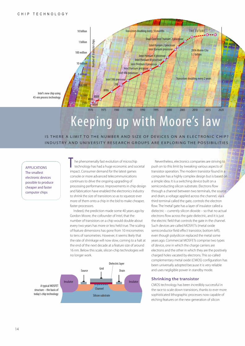
Indeed, the prediction made some 40 years ago byGordon Moore, the cofounder of Intel, that thenumber of transistors on a chip would double aboutevery two years has more or less held true. The scalingof feature dimensions has gone from 10 micrometresto tens of nanometres. However, it seems likely thatthe rate of shrinkage will now slow, coming to a halt atthe end of the next decade at a feature size of around16 nm. Below this scale, silicon-chip technologies willno longer work.
Nevertheless, electronics companies are striving topush on to this limit by tweaking various aspects oftransistor operation. The modern transistor found in acomputer has a highly complex design but is based ona simple idea. It is a switching device built on asemiconducting silicon substrate. Electrons flowthrough a channel between two terminals, the sourceand drain; a voltage applied across the channel, via athird terminal called the gate, controls the electronflow. The ‘metal’ gate has a layer of insulator called adielectric – currently silicon dioxide – so that no actualelectrons flow across the gate dielectric, and it is justthe electric field that controls the gate in the channel.Such devices are called MOSFETs (metal oxidesemiconductor field effect transistor, bottom left), even though polysilicon replaced the metal someyears ago. Commercial MOSFETs comprise two typesof device, one in which the charge carriers areelectrons and the other in which they are the positivelycharged holes vacated by electrons. This so-calledcomplementary metal oxide (CMOS) configuration hasbeen universally adopted because it is very reliableand uses negligible power in standby mode.
Shrinking the transistorCMOS technology has been incredibly successful inthe race to scale down transistors, thanks to ever moresophisticated lithographic processes now capable ofetching features on the new generation of silicon
C H I P T E C H N O L O G Y
T
I S T H E R E A L I M I T T O T H E N U M B E R A N D S I Z E O F D E V I C E S O N A N E L E C T R O N I C C H I P ?
I N D U S T R Y A N D U N I V E R S I T Y R E S E A R C H G R O U P S A R E E X P L O R I N G T H E P O S S I B I L I T I E S
Keeping up with Moore’s law
14
Dual-Core Intel ‘Itanium’ 2 processor
2006 Monte Cito1.7 billion
T H E F U T U R E . . .
2300
10,000
100,000
1 million
10 million
100 million
1 billion
10 billion
Num
ber o
f tra
nsist
or ch
ips
Intel Itanium 2 processorIntel Itanium processor
Intel Pentium 4 processorIntel Pentium III processor
Intel Pentium II processorIntel Pentium processor
Intel 486 processor
Intel 386 processor286
8086
80808008
4004
1970 1975 1980 1985 1990 1995 2000 2005 2010 2015 2020
Transistors doubling every 2 years
Transistors doubling every 18 months
Channel
Silicon substrate
Insulator Insulator
DrainSourceGrid
Dielectric layer
A typical MOSFETstructure – the basis of
today's chip technology
Intel's new chip using 45-nm process technology
APPLICATIONSThe smallestelectronic devicespossible to producecheaper and fastercomputer chips
chips as small as 90 and 65 nm. Shrinking the transistorthis far has, however, thrown up problems. Although
shortening the gate channel (so that the electronsand holes have less far to travel between the source
and drain) increases the operating speed, theamount of current passing through is also less,offsetting the overall performance of the chip. In the past three years, a new approach calledstrain engineering has been adopted toincrease the mobility of electrons in thechannel. Germanium atoms are introducedinto the crystal lattice of the silicon, whicheffectively stretch the lattice and allowelectrons to move more easily. A UK consortium
of universities and companies have beendeveloping processes to make strained silicon
devices and test their efficiency.
Leaking currentsTo scale down further to 45 nm, chip-makers have hadto tackle another issue: as the gate dielectric thins,current starts to leak through. The answer has been tolook for a replacement material for silicon dioxide witha higher dielectric constant. The best candidate turnsout to be hafnium dioxide. Unfortunately, not muchwas known about its properties as an electronicmaterial, so a huge effort has gone into itscharacterisation. Hafnium dioxide suffers from defectswhich tend to trap charge and that affects the turn-onvoltage of the transistor. Sasha Shluger and JacobGavartin at University College London, and JohnRobertson at the University of Cambridge, have beenmodelling its electronic structure on a computer to tryand understand what was causing the trapping.Another issue has been that amorphous hafniumdioxide tends to crystallise on processing, whichaffects leakage. It also reacts with silicon, reintroducingthe silicon dioxide that it is supposed to replace and solosing the benefit of the higher dielectric constant. Bymixing silicon dioxide with the hafnium dioxide to givewhat is termed ‘hafnium silicate’, the crystallisation canbe suppressed but the dielectric constant is lowered.Alan Craven and colleagues at the University ofGlasgow, in collaboration with the Belgian researchinstitute IMEC, have been studying the behaviour ofhafnium dioxide and ‘hafnium silicate’ to understandhow these materials are affected by deposition andprocessing. A further necessary development is toreplace the polysilicon gate electrode by a metallic
gate, so turning the clock full circle. Again,understanding the interaction between thin layers ofthese materials is crucial to success.
The final frontierEventually, other semiconductors capable of allowinghigher electron speeds, such as gallium arsenide,indium phosphide or germanium, will have to takeover some functions. The University of Glasgow leads alarge UK consortium investigating new devices andmaterials aimed at tackling the 22-nm scale andbeyond. In this collaboration with FreescaleSemiconductor in Arizona, the Glasgow researchersare developing a gallium-arsenide MOSFET with agallium-oxide interface capped with galliumgadolinium oxide to give low leakage. Professor Cravensays that this project has demonstrated the world’sbest performing gallium arsenide MOSFET device todate, and modelling shows that scaling to 22 nmshould be possible. Full success is likely to require‘hyper-integration’ of a number of semiconductors ona silicon platform.
Beyond this scale, MOSFETS of any material ordesign will run out of steam. It is unlikely that theycould be made with features scaling below 10 nm,when heat dissipation from the energy producedbecomes a major problem. With just a handful ofelectrons switching the transistor, quantumphenomena also take over. To achieve any furtheradvantage will mean turning to a different type oftechnology based perhaps on the spins of electrons(p.10), or on the electronic properties of molecularstructures such as carbon nanotubes (p.6) or quantumdots (p.8). Such approaches might exploit thequantum properties of single electrons and could bethe means to an entirely different type of processingbased on manipulating quantum states – quantumcomputing. One approach, that of Marshall Stonehamand his team at University College London, useselectron spins controlled by a laser in a way that iscompatible with the silicon technology of near-futurefabrication plants. Unlike most quantum computingschemes, it might even work at room temperature!
However, it could be some years before suchschemes become a commercial reality. In themeantime we can expect to see the scaling downcontinue, if not quite at the speed predicted byMoore’s law.
P H Y S I C S F O R F U T U R E T E C H N O L O G Y
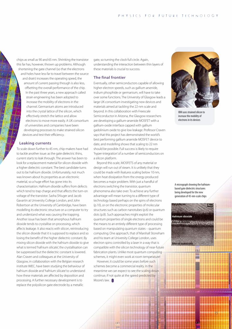
IBM uses strained silicon toincrease the mobility ofelectrons in its devices
A micrograph showing the hafnium-based gate dielectric structuresbeing developed for the newgeneration of 45-nm-scale chips
Mau
reen
Mac
Kenz
ie/
Uni
vers
ity
of G
lasg
ow
15

Nanoparticles in medicineDr Fred CurrellQueen’s University BelfastEmail: [email protected]
Dr Jon DobsonKeele UniversityEmail: [email protected]
Professor Duncan GrahamUniversity of StrathclydeEmail: [email protected]
Dr Tracy MelvinUniversity of SouthamptonEmail: [email protected]
Dr Quentin PankhurstUniversity College LondonEmail: [email protected]
Professor David RussellUniversity of East AngliaEmail: [email protected]
Wonderful carbonDr Mark EllerbyUniversity College London Email: [email protected]
Professor Andre GeimUniversity of ManchesterEmail: [email protected]
Professor Bill MilneUniversity of CambridgeEmail: [email protected]
Professor Robin NicholasUniversity of OxfordEmail: [email protected]
Dr Tom WellerSTFC Rutherford AppletonLaboratoryEmail: [email protected]
Quantum dots light up the futureDr Ray MurrayImperial College London Email: [email protected]
Dr Andrew ShieldsToshiba Research Europe,CambridgeEmail:[email protected]
Professor Maurice SkolnickUniversity of SheffieldEmail: [email protected]
Dr Peter SmowtonCardiff UniversityEmail: [email protected]
A new spin on electronicsProfessor John ChapmanUniversity of GlasgowEmail: [email protected]
Professor Russell CowburnImperial College London Email: [email protected]
Professor Bryan Gallagher University of Nottingham Email:[email protected]
Professor Bryan HickeyUniversity of LeedsEmail: [email protected]
Dr Jörg WunderlichUniversity of CambridgeEmail: [email protected]
Going with the flowProfessor Michael CatesUniversity of EdinburghEmail: [email protected]
Professor Tom McLeishUniversity of Leeds Email: [email protected]
Professor Wilson PoonUniversity of EdinburghEmail: [email protected]
Keeping up with Moore’s lawProfessor Alan CravenUniversity of GlasgowEmail: [email protected]
Professor John RobertsonUniversity of CambridgeEmail: [email protected]
Professor Marshall StonehamUniversity College London Email: [email protected]
Contacts
Xxxxxxxxxxxxxxx
16


P H Y S I C S F O R F U T U R E T E C H N O L O G Y
Condensed matter
For further information, please contact:
Tajinder PanesorThe Institute of Physics76 Portland PlaceLondon W1B 1NTUKEmail: [email protected]: www.iop.org
Jason GreenEPSRCPolaris HouseNorth Star AvenueSwindon SN2 1ETUKEmail: [email protected]: www.epsrc.ac.uk
© Institute of Physics and EPSRC 2007
Writer and editor: Nina Hall
Design: Spaced