Embed Size (px)
Citation preview

PHYSICS AND TECHNOLOGY OF THE INFRARED DETECTION SYSTEMS
BASED ON HETEROJUNCTIONS
A THESIS SUBMITTED TO
THE GRADUATE SCHOOL OF NATURAL AND APPLIED SCIENCES
OF
THE MIDDLE EAST TECHNICAL UNIVERSITY
BY
BÜLENT ASLAN
IN PARTIAL FULFILLMENT OF THE REQUIREMENTS FOR THE DEGREE OF
DOCTOR OF PHILOSOPHY
IN
THE DEPARTMENT OF PHYSICS
MARCH 2004

ii
Approval of the Graduate School of Natural and Applied Sciences
Prof. Dr. Canan Özgen
Director
I certify that this thesis satisfies all the requirements as a thesis for the degree of
Doctor of Philosophy.
Prof. Dr. Sinan Bilikmen
Head of Department
This is to certify that we have read this thesis and that in our opinion it is fully
adequate, in scope and quality, as a thesis for the degree of Doctor of Philosophy.
Prof. Dr. Raşit Turan
Supervisor
Examining Committee Members
Prof. Dr. Raşit TURAN
Prof. Dr. Özcan ÖKTÜ
Prof. Dr. Çiğdem ERÇELEBİ
Assoc. Prof. Dr. Mehmet PARLAK
Assoc. Prof. Dr. Cengiz BEŞİKÇİ

iii
ABSTRACT
PHYSICS AND TECHNOLOGY OF THE INFRARED DETECTION SYSTEMS
BASED ON HETEROJUNCTIONS
Aslan, Bülent
Ph. D., Department of Physics
Supervisor: Prof. Dr. Raşit Turan
March 2004, 127 pages
The physics and technology of the heterojunction infrared photodetectors having
different material systems have been studied extensively. Devices used in this study
have been characterized by using mainly optical methods, and electrical
measurements have been used as an auxiliary method. The theory of internal
photoemission in semiconductor heterojunctions has been investigated and the
existing model has been extended by incorporating the effects of the difference in
the effective masses in the active region and the substrate, nonspherical-
nonparabolic bands, and the energy loss per collisions. The barrier heights
(correspondingly the cut-off wavelengths) of SiGe/Si samples have been found
from their internal photoemission spectrums by using the complete model which
has the wavelength and doping concentration dependent free carrier absorption
parameters. A qualitative model describing the mechanisms of photocurrent
generation in SiGe/Si HIP devices has been presented. It has been shown that the
performance of our devices depends significantly on the applied bias and the
operating temperature. Properties of internal photoemission in a PtSi/Si Schottky
type infrared detector have also been studied. InGaAs/InP quantum well

iv
photodetectors that covers both near and mid-infrared spectral regions by means of
interband and intersubband transitions have been studied. To understand the high
responsivity values observed at high biases, the gain and avalanche multiplication
processes have been investigated. Finally, the results of a detailed characterization
study on a systematic set of InAs/GaAs self-assembled quantum dot infrared
photodetectors have been presented. A simple physical picture has also been
discussed to account for the main observed features.
Keywords: Infrared photodetectors, internal photoemission, SiGe/Si, dual-band,
quantum well, quantum dot.

v
ÖZ
ÇOKLUEKLEM TABANLI KIZILÖTESİ ALGILAMA SİSTEMLERİNİN FİZİĞİ
VE TEKNOLOJİSİ
Aslan, Bülent
Doktora, Fizik Bölümü
Tez Yöneticisi: Prof. Dr. Raşit Turan
Mart 2004, 127 sayfa
Farklı malzeme sistemlerine sahip çoklueklem kızılötesi fotoalgılayıcıların fiziği ve
teknolojisi geniş ölçüde çalışıldı. Bu çalışmada kullanılan aygıtlar, temel olarak
optiksel yöntemler kullanılarak nitelendirildi ve yardımcı bir yöntem olarak
elektriksel ölçümler kullanıldı. Yarıiletken çoklueklemlerdeki dahili ışılsalım teorisi
incelendi ve varolan model, aktif bölge ve alttaş etkin kütleleri arasındaki farkın,
küresel olmayan-parabolik olmayan bantların ve çarpışma başına düşen enerji
kaybının etkileriyle birleştirilerek genişletildi. SiGe/Si örneklerin engel
yükseklikleri (denkçe eşik dalgaboyları), dahili ışılsalım tayflarından dalgaboyu ve
katkı miktarı bağımlı özgür taşıyıcı soğurması parametrelerine sahip tam model
kullanırak bulundu. SiGe/Si HIP aygıtlardaki fotoakım oluşma mekanizmalarını
açıklayan nitel bir model sunuldu. Aygıtlarımızın performanslarının uygulanan
voltaja ve çalışma sıcaklığına önemli derecede bağlı olduğu gösterildi. PtSi/Si
Schottky tipi kızılötesi algılayıcılardaki dahili ışılsalım özellikleri de çalışıldı.
Bantlar ve altbantlar arasındaki geçişler yoluyla hem yakın hem de orta-kızılötesi
bölgeyi kapsayan InGaAs/InP kuatum kuyu fotoalgılayıcılar çalışıldı. Büyük
besleme değerlerinde gözlenen yüksek tepkiselliği anlamak için kazanç ve çığ
vi
çoğalma olayları incelendi. Son olarak, bir InAs/GaAs kendiliğinden oluşan
kuantum nokta kızılötesi fotoalgılayıcılar grubu üzerindeki ayrıntılı nitelendirme
çalışması sonuçları sunuldu. Gözlenen temel özellikleri değerlendirmek için basit
bir fiziksel resim tartışıldı.
Anahtar kelimeler: Kızılötesi fotoalgılayıcılar, dahili ışılsalım, SiGe/Si, ikili-bant,
kuantum kuyu, kuantum nokta.

vii
ACKNOWLEDGMENTS
I must express my gratitude to my supervisor Prof. Dr. Raşit Turan for giving me
the chance to work with him. His unconditional guidance and help throughout my
graduate study is a great value to me. I would also like to thank him for his
enthusiastic support as a friend.
Dr. H. C. Liu is another important person whom I must thank very much. It was my
privilege to work with him. I have greatly benefited from his knowledge and
scientific vision.
I intensely acknowledge my colleagues in the laboratories both here at METU and
at the Institute for Microstructural Sciences, National Research Council of Canada,
Ottawa for their genial attitude to me.
I would like to thank the Scientific and Technical Research Council of Turkey
(TUBITAK) for financial support during my stay at the National Research Council,
Canada.
Finally, I would like to express my endless gratitude to my parents, without whom I
would not have had the opportunity to carry on this study.

viii
TABLE OF CONTENTS
ABSTRACT ............................................................................................................. iii
ÖZ ............................................................................................................................. v
ACKNOWLEDGMENTS ....................................................................................... vii
TABLE OF CONTENTS ........................................................................................ vii
LIST OF FIGURES .................................................................................................. xi
LIST OF TABLES ................................................................................................. xvi
CHAPTER
1. INFRARED DETECTORS ....................................................................... 1
1.1 Introduction ...................................................................................... 1
1.2 Photon Detectors .............................................................................. 3
1.2.1 Mercury Cadmium Telluride (HgCdTe) Photodiodes ......... 4
1.2.2 Schottky Barrier Infrared Photodetectors ............................ 5
1.2.3 Heterojunction Internal Photoemission (HIP) Detectors ..... 6
1.2.4 Blocked Impurity Band (BIB) Detectors ............................. 6
1.2.5 Homojunction Internal Photoemission Detectors ................ 6
1.2.6 Quantum Well Infrared Photodetectors (QWIP) ................. 7
1.2.7 Quantum Dot Infrared Photodetectors (QDIP) .................... 8
1.3 Thermal Detectors ............................................................................ 8
1.3.1 Bolometers ........................................................................... 9
1.3.2 Pyroelectric Detectors .......................................................... 9
1.3.3 Thermoelectric Detectors ................................................... 10
2. THEORY OF INTERNAL PHOTOEMISSION IN
HETEROJUNCTIONS ............................................................................ 11

ix
2.1 Model for Escape Probability ......................................................... 13
2.2 Band Correction over Effective Mass ............................................ 24
2.3 Effects of Multiple Reflections and Scattering .............................. 28
2.4 Quantum Mechanical Effects ......................................................... 34
2.5 Effect of e-p Collisions and Energy Losses ................................... 34
2.6 Analysis: Effects of the Scattering Parameters on the Yield ......... 37
2.7 Infrared Absorption ........................................................................ 42
3. MECHANISMS OF PHOTOCURRENT GENERATION IN SiGe/Si
HIP INFRARED PHOTODETECTORS ................................................ 45
3.1 Experimental Details and Device Operation .................................. 46
3.1.1 Device Operation ............................................................... 48
3.2 Spectral Photoresponse and a Simple Model ................................. 49
3.2.1 Fowler Analysis ................................................................. 53
3.3 Responsivity versus Voltage .......................................................... 55
3.4 I-V Characteristics and Activation Energy Analysis ..................... 57
3.5 Samples with Different Parameters ................................................ 59
4. DOUBLE-BARRIER LONG WAVELENGTH SiGe/Si HIP
INFRARED PHOTODETECTORS ........................................................ 63
4.1 Experimental Details ...................................................................... 63
4.2 Experimental Results and Discussions on the Double-Barrier
SiGe/Si HIP .................................................................................... 65
4.2.1 Spectral Photoresponse ...................................................... 65
4.2.2 Fowler Analysis and Responsivity .................................... 67
4.2.3 I-V and Activation Energy Analysis .................................. 69
5. INTERNAL PHOTOEMISSION SPECTROSCOPY FOR PtSi/p-Si
INFRARED DETECTORS ..................................................................... 73
5.1 Internal Photoemission in Metal/Semiconductor Systems ............. 74
5.2 Experimental Details ...................................................................... 77
5.3 PtSi/p-Si Spectrum ......................................................................... 79
5.4 Effect of the Ice Formation on the Detector’s Response ............... 80
5.5 I-V Characteristics of PtSi/p-Si Diodes ......................................... 83
6. InGaAs/InP QUANTUM WELL INFRARED PHOTODETECTORS .. 87

x
6.1 Basic principles of QWIPs ............................................................. 88
6.2 InGaAs/InP Dual-Band QWIP ....................................................... 90
6.3 Experimental Details ...................................................................... 91
6.4 Spectral Photoresponse .................................................................. 91
6.5 Responsivity versus Voltage .......................................................... 94
6.6 Noise and Avalanche Multiplication .............................................. 94
7. DETAILED CHARACTERIZATION OF A SYSTEMATIC SET OF
QUANTUM DOT INFRARED PHOTODETECTORS ......................... 99
7.1 Anticipated Advantages of QDIPs ............................................... 100
7.2 Experimental Details .................................................................... 103
7.3 Physical Picture ............................................................................ 104
7.4 Results and Discussion ................................................................. 107
8. CONCLUSION ...................................................................................... 113
REFERENCES ...................................................................................................... 116
VITA ..................................................................................................................... 125

xi
LIST OF FIGURES
FIGURE
1.1 Transmission spectrum of the atmosphere ................................................. 2
2.1 Valence band profile and the energy levels.............................................. 13
2.2 Distribution of holes in momentum space for a spherical Fermi
surface at 0 K. a) hν < EF, b) hν > EF ...................................................... 15
2.3 3D graphical representation of the carriers in momentum space for m2
(=0.6 m0) > m1. a) m1 = 0.3 m0, b) m1 = 0.55 m0, c) Floating 3D view
of the system showing the intersection..................................................... 17
2.4 3D graphical representation of the carriers in momentum space for a)
m2 = m1 = 0.6 m0, b) Floating 3D view of the system showing the
intersection................................................................................................ 18
2.5 3D graphical representation of the carriers in momentum space for m2
(=0.6 m0) < m1. a) m1 = 0.7 m0, b) m1 = 0.9 m0, c) Floating 3D view
of the system showing the intersection..................................................... 19
2.6 Escape volume for holes in momentum space for three different cases
(the hatched region corresponds to the holes that may escape over the
barrier). a) m(SiGe) < m(Si), b) m(SiGe) = m(Si), c) m(SiGe) > m(Si) .. 20
2.7 Geometrical definitions of the parameters in momentum space .............. 21
2.8 Calculated effective mass and Fermi energy versus doping
concentration graph for different x values at 4 K (from reference
[69]) .......................................................................................................... 24
2.9 Calculated yields versus photon energy graph for different M values
when the constant effective mass is considered ....................................... 25

xii
2.10 Calculated yields versus effective masses ratio M for different photon
energies when the constant effective mass is considered ......................... 26
2.11 Calculated yields versus photon energy graph for different M values
when the energy dependent effective mass is considered ........................ 27
2.12 Calculated yields versus effective masses ratio M for different photon
energies when the energy dependent effective mass is considered .......... 27
2.13 a) 3-dimensional representation of the variation of the yield with
respect to the effective masses ratio and the energy of the incident
photons. b) The projections of the 3D surface on each plane in the
shaded form .............................................................................................. 28
2.14 The effect of different substrate (Si in this case) effective masses on
the yield .................................................................................................... 29
2.15 Schematic diagram showing the different processes during the motion
of an excited carrier before emission........................................................ 30
2.16 Diagram illustrating the definition of the spherical shell of emission...... 33
2.17 Effect of the film thicknesses on the yield versus energy plots................ 38
2.18 Yield versus energy plots for several hot-hole/phonon scattering
mean free paths (Lp) with an energy loss per collision (ћω) of a) 1
meV, and b) 10 meV................................................................................. 39
2.19 Yield versus energy plots for several hot-hole/cold electron scattering
mean free paths (Le).................................................................................. 40
2.20 Effect of the energy loss per collisions (ћω) term on the yield ................ 41
2.21 Yield versus energy plots for different Fermi energies ............................ 41
2.22 Variation of the yield with different barrier height values ....................... 42
2.23 a) External yield (product of the internal yield and the optical
absorption) versus energy plot, b) same graph in the form of Fowler
plot ............................................................................................................ 44
3.1 Schematic device structure with layer thicknesses and the valence
band edge profile showing the basic operation principle of the
SiGe/Si HIP investigated here .................................................................. 47

xiii
3.2 The schematic representation of a device: (a) cross-section of the
device and (b) the top view of the mesa with ring shaped Al ohmic
contact....................................................................................................... 48
3.3 Responsivity measurement setup.............................................................. 48
3.4 Spectral photoresponse curves under different bias conditions at 10
K. The voltage values written in the legend are the potential
differences across the device when it is illuminated by the light
coming from the IR source. The inset shows the change in the
photovoltage with the applied bias for 10 K measurements..................... 50
3.5 Qualitative physical picture for interpreting the experimental results.
The potential difference is negative for (a) and positive for (b). The
bottom contact is the ground and arrows show the direction of the
photoexcited holes’ direction.................................................................... 52
3.6 Fowler plot of the experimental data (circles) and the theoretical fit
(solid lines) for the device biased with 75 mV and -37 mV..................... 54
3.7 Responsivity versus voltage characteristics of the device at different
temperatures. Measurements have been performed at 7.14 µm .............. 56
3.8 Semilogarithmic plot of I-V characteristics of the sample under
different experimental conditions............................................................. 58
3.9 Activation energy plot for determination of barrier height ...................... 58
3.10 Spectral photoresponse curves for a set of samples. Samples were
biased with 75 mV except 1105 which is biased with 20 mV.................. 60
3.11 Activation energy plots for determination of barrier height (for the
entire set of samples) ................................................................................ 61
3.12 Responsivity versus voltage characteristics of the devices at 10 K.
Measurements have been performed at 8.06 µm, 8.06 µm, 7.14 µm,
6.67 µm, and 6.25 µm, respectively ......................................................... 62
4.1 Schematic device structure with layer thicknesses for both sample
1111 and sample 1105 (a) and the valence band edge profile showing
the operation principle (b) ........................................................................ 65
4.2 Spectral photoresponse curves under positive bias at different
temperatures for sample 1111 (a) and for sample 1105 (b) under

xiv
small positive bias. Applied bias values are 250 mV (10 K), 200 mV
(20 K), 125 mV (30 K), and 30 mV (50 K) for sample 1111. As for
sample 1105, 20 mV was applied at both temperatures. Note that 20
K spectrum was multiplied by 10............................................................. 66
4.3 Responsivity versus voltage characteristics of the sample 1111 at
different temperatures; 10 K and 50 K. Measurements have been
performed at 5.8 µm ................................................................................. 68
4.4 Fowler plots of internal photoemission spectra for the sample 1111 at
10 K and 50 K........................................................................................... 69
4.5 Semilogarithmic plot of I-V characteristics of the samples 1111 and
1105 under different experimental conditions.......................................... 71
4.6 Activation energy plot for determination of barrier height ...................... 72
5.1 Energy levels in metal-semiconductor band structure.............................. 75
5.2 Escape cap for holes in momentum space. The hatched region
corresponds to the holes that may escape over the barrier ....................... 76
5.3 Cross-section of the PtSi/p-Si diodes ....................................................... 77
5.4 Optoelectronic spectrum measurement system ........................................ 78
5.5 Internal photoemission spectrum of the PtSi/p-Si diode. Curves fitted
by modified Fowler theory and extended theory are also shown ............. 80
5.6 a) Effect of different vacuum conditions on the internal
photoemission spectrum of the PtSi/p-Si diode. b) Direct comparison
of the observed dip to the spectrum of the ice taken from Ref. [109].
(Experimental data are normalized against the theoretical response
curve). The solid line (ice’s absorption spectrum) belongs to the left
axis and the others (experimental data) belong to the right axis.
Marker types are same as (a) .................................................................... 81
5.7 I-V characteristics of the PtSi/p-Si diode at different temperatures for
(a) forward and (b) reverse bias. Fitted lines for the extraction of the
barrier height and the ideality factor are also shown................................ 84
6.1 Density of states versus energy for 0, 2, and 3-dimensional carries ........ 88
6.2 Schematic band diagram of a quantum well showing the basics of
infrared absorption: Intersubband absorption can take place between

xv
the energy levels of a QW associated with the conduction or valence
band while the interband absorption is between the bands ...................... 89
6.3 a) Schematic energy-band diagram of the device used here under
bias. The arrows indicate the processes for dual-band detection. b)
45o facet measurement geometry for the light coupling........................... 92
6.4 Spectral photoresponse curves for samples 235 and 236 at device
temperature of 77 K. The two parts are separately normalized. The
spectral shapes are insensitive to the bias values and voltages in the
range of 2 – 3 V are used for the curves shown ....................................... 93
6.5 Responsivity versus voltage characteristics of (a) sample 235 and (b)
sample 236 at device temperature of 77 K. Measurements in MIR
were performed at 9.4 and 8.6 µm for samples 235 and 236,
respectively. For NIR calibration 0.96 µm light was used for both
devices ...................................................................................................... 95
6.6 a) Dark current (density) versus voltage characteristic, and b)
photoconductive gain phg and noise gain ng , and the ratio ( phn gg / )
of the two gains versus voltage for sample 236. The latter is the
excess noise factor F which approximately equals the multiplication
factor M..................................................................................................... 97
7.1 Schematic (a) layers of a QWIP and QDIP and (b) potential profile
for both structures under bias ................................................................. 101
7.2 Schematic conduction band inter-shell transitions in a self-assembled
InAs/GaAs quantum dot. Solid and dotted arrows represent
transitions for E//z and E//x-y polarized lights, respectively. The top
part is for transitions originating from the s shell, and the bottom for
p shell...................................................................................................... 106
7.3 Dark current characteristics for all samples at two different
temperatures, 77 K (a) and 6 K (b)......................................................... 108
7.4 Comparison of mid-infrared photoresponse curves of samples having
different numbers of electrons per dot for (a) P-polarized and (b) S-
polarized lights. The P-spectra are normalized to unity, while the S-

xvi
spectra are scaled by the same amounts for comparison. The inset to
the bottom panel shows the experimental geometry .............................. 109
7.5 Normalized far-infrared photoresponse curves for (a) P-polarized and
(b) S-polarized lights. To compare the relative magnitudes between P
and S responses, the lower panel curves should be multiplied by 0.6,
0.8, and 3.8 for sample A, B, and C, respectively, for example, the
solid curve in (b) should be multiplied by 0.6 to compare with the
curve in (a).............................................................................................. 111
7.6 Responsivity versus voltage characteristics for samples A, B and C at
7.14 µm (174 meV) and 6 K................................................................... 112

xvii
LIST OF TABLES
TABLE
3.1 Structural parameters of the samples........................................................ 60
3.2 Parameters used in Fowler analysis and the barrier height values
obtained from both electrical and optical measurements ......................... 62
5.1 Barrier height and ideality factor (n) values extracted from I-V
analysis of PtSi/p-Si diodes at various temperatures................................ 85
5.2 Barrier height values of PtSi/p-Si obtained by I-V analysis and
internal photoemission spectroscopy (IPS) analysis ................................ 86
7.1 Structural parameters obtained from atomic force microscopy and
plan-view transmission electron microscopy observations to estimate
the number of the electrons per dot ........................................................ 104

1
CHAPTER 1
INFRARED DETECTORS
1.1 Introduction
Infrared (IR) spectrum is a part of the electromagnetic spectrum: It is defined as the
region just above the visible (0.7 µm) to millimeter waves (1000 µm). This is the
region where every object having non-zero temperature emits “thermal radiation”.
The characteristics of this radiation depend on the temperature and the wavelength.
Since the human eye responds well to the visible light but poorly to infrared
radiation, almost all the information encoded in the infrared radiation is not directly
detected by the human eyes. Therefore, it is necessary to develop a device if thermal
radiation is to be detected.
The interest in the detection of IR radiation has centered mainly on the two
atmospheric windows, 3-5 µm and 8-12 µm, based on two facts: (i) Most of the
energy emitted by an object at around room temperature is in 3-14 µm wavelength
region [1]. (ii) Atmospheric transmission is the highest in these windows. Fig. 1.1
shows the infrared transmission over a spectral range from 0.7 µm to 15 µm [2]. In
recent years, along with the technological development/progress, there has been
increasing interest in longer wavelengths stimulated by space applications.
The main function of a detector is the conversion of the radiation falling on it into
an electrical signal for further investigation. This can be done by using many
different physical phenomena. IR detectors are divided into two basic groups;
photon detectors (or photodetectors) and thermal detectors which differ by the

2
physical mechanism used for the detection process. In the photon detectors, the
radiation is absorbed within the material by interaction with electrons either bound
to lattice atoms or to impurity atoms or with free electrons. This interaction
produces parameter changes (such as voltage, current, resistance etc.) that are
detected by external measurement circuits. As in thermal detectors, the radiation
must alter the temperature of the sensor resulting in the change in some basic
property of the device. Thermal detectors produce a signal that is independent of
energy or wavelength, while photon detectors are dependent on the number of
photons and their energy.
Fig. 1.1 Transmission spectrum of the atmosphere.
This thesis is designed in a way that each chapter is self-contained. This chapter is
devoted to the general discussion of infrared detectors. In chapter 2, the theory of
internal photoemission in semiconductor heterojunctions is discussed and a
complete model is derived. In chapters 3 and 4, SiGe/Si HIP infrared photodetectors
are characterized by optical and electrical methods. Additionally, a qualitative
model describing the photocurrent generation mechanisms is presented. PtSi/Si
Schottky type infrared photodetectors are given in chapter 5. In the following
chapter (chapter 6), InGaAs/InP dual-band quantum well infrared photodetectors
showing high responsivity feature at high biases are presented. Finally, the results

3
of a detailed characterization study on a systematic set of InAs/GaAs self-
assembled quantum dot infrared photodetectors are presented in chapter 7. All
samples except PtSi/Si ones used in this study were grown and processed at the
Institute for Microstructural Sciences, National Research Council, Ottawa, Canada.
1.2 Photon Detectors
Photon detectors are quantum counters where the incident photons create electrons
that are conducted to the external measurement circuit. They are usually
characterized by a minimum energy of photon detection or, equivalently, a long
wavelength cut-off beyond which the device has no response to the incident photon.
Photon detectors having long wavelength limits (>3 µm) generally need to be
cooled to achieve good signal-to-noise ratio and a fast response.
Depending on the nature of the interaction, the photon detectors are divided into
sub-groups: Intrinsic detectors (e.g. PbS, PbSe, HgCdTe, InGaAs, InAs, InSb etc),
extrinsic detectors (e.g. Si:Ge, Si:As, Ge:Cu etc.), free carrier detectors (PtSi, IrSi
etc.), quantum well detectors (GaAs/AlGaAs, InGaAs/AlGaAs, InAs/InAsSb, etc.),
and quantum dot detectors (InAs/GaAs, Ge/Si, etc). Depending also on how the
electric signal is developed, there are various modes such as photoconductive,
photovoltaic, and photoemissive ones. There are several detailed review articles and
texts on these photon detectors in the literature [3-12].
Detectors are characterized by figures of merit that allow comparison of different
detectors. The most important figure of merit is the responsivity of the
photodetector which is determined by the quantum efficiency, η, and the gain, g, if
available, and can be written as [5]
gehc
R c ηλ
= (1.1)
where λc is the cut-off wavelength of the detector. The quantum efficiency value
describes how well the detector is coupled to the radiation to be detected. It is
usually defined as the number of carriers generated per incident photon. The idea of

4
gain is proposed as a simplifying concept for the understanding of photoconductive
phenomena [13] and defined as the number of carriers passing contacts per one
generated carrier. There are some other figures of merit which are not mentioned
here such as noise equivalent power (NEP), detectivity (D*), photon-noise-limited
performance, etc., since they are not the main emphases of the thesis.
In the following sub-sections, some of the important photon detectors are presented
for the sake of completeness.
1.2.1 Mercury Cadmium Telluride (HgCdTe) Photodiodes
From fundamental considerations Mercury-Cadmium Telluride (MCT) is the most
important and worldwide attracted semiconductor alloy system for IR detectors in
the spectral range between 1 and 25 µm [8, 14 and references therein]. This material
is a ternary compound that alloys two binary compounds HgTe and CdTe. Its
chemical formula is defined as Hg1-xCdxTe. By tailoring the composition ratio of
the material (i.e. x value in Hg1-xCdxTe), the energy gap of this material varies from
semimetallic for HgTe (x = 0) with a gap of -0.3 eV to semiconducting CdTe (x =
1), which has a gap of 1.65 eV [15]. The negative sign for HgTe shows that the
bottom of the conduction band is lower than the top of the valence band. Thus, the
longer wavelength response can be achieved by increasing the Hg percentage in the
compound. These detectors are made by building a p-n junction and the optical
absorption occurs at or near the junction. If a photon with sufficient energy is
absorbed in photoactive region, an electron will gain sufficient energy to move into
the conduction band and leave a hole behind. With the movement of these
photogenerated electron-hole pair to the detector’s terminal a current flow is set up.
Note that they can also be designed as a photoconductive detector by using a slab of
material in which the created electron-hole pairs are separated by the applied bias.
Therefore, the bandgap energy determines the cut-off wavelength of the detector.
On the other hand, it is not easy to determine the bandgap of this material: As is
typical of most semiconductors, CdTe has a bandgap that decreases with
temperature. However, the bandgap energy of HgTe is increases with temperature
[16]. Therefore, various empirical expressions have been developed relating the

5
bandgap energy to the temperature T and the fraction x of cadmium. The most
accurate expression relying on data from several different studies is given as [17]
Eg = –0.302 + 1.93 x + 5.35 (10–4) T (1–2 x) – 0.810 x2 + 0.832 x3 (1.2)
Another important advantage of this material is its “intrinsic” behavior. Since the
intrinsic energy gap determines the wavelength response, the cooling requirement is
not as severe as for extrinsic detectors; because, the absorption of the radiation is
due to the bulk material HgCdTe, not the impurities.
1.2.2 Schottky Barrier Infrared Photodetectors
The metal/semiconductor contacts have been studied extensively since they have an
important role in microelectronics technology as well as their wide range of
practicability to the very large scale integration (VLSI) technology [18,19, and
references therein]. If a semiconductor is brought into a physical contact with a
metal, a rectifying or an ohmic contact is formed, depending on the type of metal
and semiconductor used. The formation of an electronic barrier at the junction is the
most important feature of a metal-semiconductor junction. The physical mechanism
responsible for this formation has been studied for many years [20,21]. Various
models using different physical concepts have been proposed and used [22-25].
In this type of detectors, light is absorbed in the metal/silicide side of the junction
and creates a “hot” carrier which passes over the potential barrier; this process is
known as internal photoemission (IP). The internal photoemission process is
discussed in details in the following chapters.
The variety of metals (or their silicides) can be used to make the Schottky barrier.
On condition of using a p-type Si substrate, the most important Schottky junction is
made of platinum (Pt → PtSi), which produces a response to ~5.6 µm [26]; other
possibilities include palladium (Pd → Pd2Si) out to ~3.5 µm [26], and iridium (Ir →
IrSi) out to ~10 µm [27,28]. All these are of interest primarily because they are
suitable for the standard silicon VLSI processing.

6
1.2.3 Heterojunction Internal Photoemission (HIP) Detectors
The heterojunction internal photoemission (HIP) detector is entirely analogous to
the Schottky type detector: The metal or silicide electrode is replaced by
degenerately doped another semiconductor material. The idea of Schottky barrier
photodiode with a degenerate semiconductor active region is first proposed by
Shephard et al. [29] and is first demonstrated by Lin et al. [30] for SiGe/Si system.
HIP detectors offers higher internal quantum efficiency compared to the Schottky
barrier detectors. There are two main reasons; (i) photons can excite carriers from
the states far below the Fermi level such that they do not gain sufficient energy to
overcome the barrier in Schottky type detectors. In contrast, narrow band of
absorbing states in the SiGe layer of the HIP detector leads to more energetic
carriers. (ii) Photoexcited holes traveling over the barrier are less likely to be
backscattered from the heterojunction interface because of the more favorable ratio
of effective masses. However, the absorption coefficient for SiGe is less than that of
the silicide or metal due to the lower free carrier density.
1.2.4 Blocked Impurity Band (BIB) Detectors
A blocked impurity band (BIB) detector is an example of the extrinsic detectors. It
is first conceived by Petroff and Stapelbroek [31]. The extrinsic Si:As detector was
reported with high sensitivity and quantum efficiency in far infrared region (to 28
µm) [32]. The BIB detector resembles the photovoltaic detector in its operation. It
has a heavily doped donor band in silicon and an undoped blocking layer is
introduced to the structure to prevent dark current from dominating the carriers. The
detailed operating principles described by an analytical model for the figure of merit
of a BIB detector can be found in [33].
1.2.5 Homojunction Internal Photoemission Detectors
Homojunction internal photoemission detectors are novel detectors for basically
very far infrared detection. The basic structure of these detectors consists of a
heavily doped layer, which acts as the IR absorber region, and an intrinsic (or
lightly doped) layer, across which most of the external bias is dropped. Therefore,

7
the barrier height depends on the applied bias. The concept of homojunction IR
detector was first proposed by Tohyama et al. [34] with the cut-off wavelength of
12 µm. Later they reported a silicon homojunction IR detector having an active PtSi
layer with extended cut-off wavelength of 30 µm [35]. Various detector approaches
(depending on the doping amount) based on Si and GaAs homojunction IP junctions
have been discussed by Perera et al. [36,37]. They obtained >40µm cut-off
wavelength.
1.2.6 Quantum Well Infrared Photodetectors (QWIP)
The concept of light detection by using quantum wells has been studied extensively
by many researchers for more than 25 years. The earliest studies were on two
dimensional electron systems in metal-oxide-semiconductor inversion layer that has
triangular barrier [38, and references therein]. Possibility of using quantum wells
with rectangular barrier for infrared detection was first suggested by Esaki and
Sakaki [39]. The first experiment on making use of quantum wells for IR detection
was reported by Smith et al. [40]. Their device operation was based on the
absorption of the IR radiation by the free carriers which are trapped in the wells
formed by GaAs/AlGaAs heterojunction material systems. Quantum wells are
constructed by growing a lower bandgap material (i.e. GaAs) between two larger
bandgap materials (i.e. AlGaAs). Therefore, the larger bandgap material serves as a
barrier while the small bandgap material serves as a well. When the width of the
well is small enough, discrete energy levels are created in the well. Intersubband
transition (ISBT) in the wells is the base of modern quantum well infrared detectors.
The prediction and the first observation of ISBT in quantum wells was reported by
West and Eglash [41]. The first clear demonstration of quantum well infrared
photodetectors (QWIPs) was made by Levine et al. [42]. Since then tremendous
progress has been made on both experimental and theoretical considerations about
QWIPs and can be found in the literature [12,43,44].

8
1.2.7 Quantum Dot Infrared Photodetectors (QDIP)
With the success of quantum well (QW) structures for the infrared detection, the
quantum dot infrared photodetector (QDIP) has attracted a lot of interest in recent
years. In general, QDIPs are similar to QWIPs but with the quantum wells replaced
by quantum dots in which electrons have discrete energy levels created by the three
dimensional confinement [45]. Quantum dots used in the detection of infrared
radiation are generally formed by the process called Stranski-Krastanov: when the
thickness of the film with the larger lattice constant exceeds a certain critical
thickness, the compressive strain within the film is relieved by the formation of
coherent island. These islands may be quantum dots called self-assembled QDs.
Because of this self assembling process, dots show large inhomogeneity both in size
and in vertical alignment. Some efforts on size and shape engineering can be found
in [46,47 and references therein].
There are several material systems used in QDIP applications. Most widely studied
one is InAs dots on GaAs substrate (i.e. InAs/GaAs) [48-50]. Another important
material system consists of Ge dots on Si substrate (Ge/Si) [51-53].
1.3 Thermal Detectors
Thermal detectors are made of materials whose physical properties change in the
presence of radiant heat. The most common thermal detectors are; (i) bolometers,
where temperature change produces a change in the resistance of the bulk material;
(ii) pyroelectric detectors, where temperature change produces a change in the
surface charge of the material; and (iii) thermocouples, where temperature change
produce a change in voltage at the junction of two different solid state materials.
Thermal detectors are important because they offer uncooled operation and cover a
large portion of the infrared spectrum. Basically the detector is suspended on lags
which are connected to the heat sink. Different from the photon detectors, thermal
detectors respond to the intensity of absorbed radiant power without regarding to
spectral content. In other words, they respond equally well to all photon

9
wavelength. Since they work based on the heat flow in the device, heat balance
equations are an important consideration when analyzing these devices.
1.3.1 Bolometers
A bolometer is the thermal analogue of a photoconductor. The effect is that of
change in resistivity of a material in response to the heating effect of incident
radiation. In contrast to photoconductors, bolometers can be made of any material
which exhibits temperature dependent change of resistance. The temperature
dependence is specified in terms of the temperature coefficient of resistance α
defined as [5]
d
d
d dT
dR
R
1=α (1.3)
where Rd is the detector resistance and Td is the detector temperature. The electrical
circuit requires a voltage source to measure the change in resistance due to the
heating effect of the radiation.
1.3.2 Pyroelectric Detectors
Pyroelectric detectors were developed to be worked as a sensitive uncooled
detector. They have wide spectral response. Pyroelectric detectors are made from
ferroelectric crystals, that is, crystals that can exhibit a permanent electric dipole
moment even in the absence of an applied electric field [54]. Lithium tantalite and
triglycerine sulfate are the most common detector materials. If the temperature of
such material is altered, the electric dipole moment of the crystal must change,
leading to the motion of bound charge. If electrodes are placed on the surfaces of
the crystal, this motion can induce a current flowing through the external circuit.
The magnitude of this current is given by [55]
dt
dTApi d= (1.4)

10
where A is the area of the electrode and p is the pyroelectric coefficient. This
process is independent of the wavelength of the radiation and hence pyroelectric
sensors have a flat response over a very wide spectral range.
1.3.3 Thermoelectric Detectors
In a circuit consisting of two different conductors and the junctions between them,
preferential heating of one junction will generate a voltage which is a measure of
temperature difference. When the temperature difference arises from the absorption
of radiation at one junction, the device is known a radiation thermocouple. In order
to increase the signal voltage, they are connected in series to form a radiation
thermopile.
Radiation thermopiles are generally made by subsequent evaporation of metal films
such that they are partly overlapped forming a junction. They require no electric
bias. They have been found to be useful in spaceborne applications. The preparation
and properties of radiation thermopiles can be found in review article [56].
11
CHAPTER 2
THEORY OF INTERNAL PHOTOEMISSION IN HETEROJUNCTIONS
Internal photoemission is the process in which a carrier is created / excited by an
incoming photon, transported to another region and detected as an electric signal.
To understand the photon-detection process, the concept of converting a photon of
light into an electron must be investigated and for whole process a model must be
developed. The efficiency of converting a photon to an electron is defined as
quantum efficiency and it takes into account reflectance, absorptance, scattering and
electron recombination.
The internal photoemission studies started after R. H. Fowler [57] developed a
model describing the response characteristics of the photoemission from metal into
vacuum in 1931. According to the theory, photoelectric sensitivity or number of
electrons emitted per quantum of light absorbed is proportional to the number of
electrons per unit volume of the metal whose kinetic energy normal to the surface
augmented by incident photon energy hν is sufficient to overcome the potential step
at the interface. This is the basic statement for the later studies. In late 1960’s
internal photoemission in a metal-semiconductor junction was first studied by
Cohen et al. [58] without taking into account the optical absorptance and the carrier
scattering. In this approach, a geometrical analysis was applied to derive the
photoyield in the photoemission process. Moreover, several simplifications were
assumed to make photoemission model tractable and to drive an equation known as
“modified Fowler equation”. Then the theory must have been further extended,
taking into account multiple reflections of the excited electrons from the surfaces of

12
the metal film, in addition to collisions with phonons, imperfections, and cold
electrons. Vickers [59] and Dalal [60] each developed a ballistic transport model
independently in 1971. They showed that the redistribution of momentum by
phonon and wall scattering (which can redirect the hot-hole momentum so that it
falls in the escape volume) increases the yield. Later, the model was advanced by
Mooney and Silverman [61,62] in 1985. They incorporated the “counting loss
correction” and “energy loss” terms to the model.
During this period, the idea of utilizing the internal photoemission over a
heterojunction barrier for infrared detection was first proposed by Shepherd et al. in
1971 [29]. The idea was very attractive since it is possible to control the barrier
height and to improve the quantum efficiency. However, the technology was not
available at that time to demonstrate the operation of heterojunction infrared
detector. It was 1990 that the first Si1-xGex/Si heterojunction internal photoemission
(HIP) infrared (IR) photodetector was demonstrated by T. L. Lin and J. Maserjian
[30]. With the development of molecular beam epitaxy (MBE), several works on
heterojunction infrared detectors have been reported [63-66]. A theoretical model
for the quantum efficiency of the Si1-xGex/Si HIP detector was reported by Tsaur et
al. [63]. In the model, the internal yield was calculated through the integration of
density of states. Nevertheless, it was developed for the region hν > EF, and the
wavelength dependent absorption was not considered, which made model not
applicable for the determination of the optical barrier. This is because the Fermi
energies in such structures are usually quite high due to the high doping
concentration. The model which includes these aspects was then developed by Lin
et al. in 1994 [67]. But, neither of these models was including scattering
mechanisms that the carriers experienced during their motion. Another model
taking into account the scattering of excited carriers was reported by Strong et al.
[65,68]. In this model, they followed the model which was developed for the
metal(silicide)/semiconductor systems by Vickers [59] and incorporated the
wavelength and doping concentration dependent absorption. The model comprises
several assumptions and needs to be improved.

13
In this chapter, an extended model, whose contents are similar to that of Mooney’s
extended model [61], for semiconductor heterojunction internal photoemission
detectors is presented. The extensions incorporate the effects on the yield of the
difference in the effective masses in the active region and the substrate,
nonspherical-nonparabolic bands, and the energy loss per collisions. Before
analyzing the effect of the nonspherical-nonparabolic bands on the yield, different
equations are derived for the yield for different regions depending on the relative
magnitudes of the photon’s energy, Fermi level position and the barrier height
considering the relation between the magnitudes of the effective masses in both
sides of the interface in the next section. In section 2.2 band corrections over the
effective mass is discussed. Sections 2.3 – 2.5 present effects of several physical
mechanisms such as wall reflection, hot carrier-phonon collision, quantum
mechanical reflection, e-p collisions and energy losses. The results of theoretical
calculations as a function of different material parameters are presented in section
2.6. Finally in the last section, the model is completed by incorporating the
wavelength and doping concentration dependent free carrier absorption to the
model.
2.1 Model for Escape Probability
Quantum efficiency (namely external photoyield) can be taken as the product of the
absorption of the incident photons and the internal yield which describes the
photocurrent generation mechanisms inside the structure after the photons have
been absorbed:
iext YAY = (2.1)
Here A is the optical absorption of the active layer as a function of wavelength and
doping concentration, and iY is the internal photoyield. We first demonstrate the
model describing internal yield.
Fig.2.1 shows the valence band profile and the energy levels for a SiGe/Si HIP
structure. For SiGe heterojunction detectors with a degenerately doped SiGe layer,

14
Fig. 2.1 Valence band profile and the energy levels.
holes populate states from the valence band to the Fermi level. When T = 0K all
states up to Fermi level is full of carriers and there is no hole above the Fermi level.
Note that, energy value of the valence band edge of the SiGe layer has been taken
as 0 eV. Excited holes are generated in the active region through the free carrier
absorption of photons. Some of these holes reach the SiGe/Si interface, where they
can be emitted over the potential barrier created by the valence band offset between
strained p+-Si1-xGex and p-Si. Depending on the relative magnitudes of (hν) and the
EF, distribution of excited holes can be written in momentum space as
k(EF) < k < k(EF+hν), hν < EF (2.2a)
k(hν) < k < k(EF+hν), hν > EF (2.2b)
Schematic representation of the excited holes’ distributions for both hν < EF and hν
> EF are shown in Fig.2.2. If the spherical-parabolic band is considered for the
holes at the SiGe and the Si layers, the condition for the conservation of total energy
is found to be
2
22
1
22
22 m
kE
m
kF
′+Φ+=hh
(2.3)
Here m1 and m2 are the effective masses in the SiGe film and the Si substrate
respectively, k is the magnitude of the hole’s wave vector in SiGe and k′ is that of
in silicon substrate. Momentum can be divided into two parts; parallel and
photon hν Φ
p+-Si1-xGex p-Si 0
EF EV

15
perpendicular components with respect to the barrier ( 2//
22 kkk += ⊥ ). Imposing the
conditions that the final kinetic energy directed normal to the barrier ( 122 2/ mk⊥h )
must be grater than zero and that the parallel momentum is conserved ( //// kk ′= ),
one obtains
Φ+≥
−+⊥
FEkmmm
k 2//
21
2
1
22 11
22
hh (2.4)
Fig. 2.2 Distribution of holes in momentum space for a spherical Fermi surface at 0
K. a) hν < EF, b) hν > EF.
For Eq. (2.4), magnitudes of the effective masses determine what kind of equality is
satisfied in k-space:
i. For m2 > m1, an ellipsoid satisfies the equality with the equation
12
2//
2
2
=+⊥
b
k
a
k (2.5)
where
k(EF + hν)
k(EF)
Spherical shell of
excitation
k(hν)
k(EF + hν)
( a ) ( b )

16
( ) 21
2 /2 hΦ+= FEma and ( )( )2/1
12
221
2 /2mm
mEmb F
−Φ+= h
ii. For m2 = m1, a plane which is parallel to the interface satisfies the equality with
the equation
12
2
=⊥
a
k. (2.6)
iii. For m2 < m1, a two-sheeted circular hyperboloid oriented along the ⊥k direction
satisfies the equality with the equation
12
2//
2
2
=−⊥
b
k
a
k. (2.7)
When the relative magnitudes of a and b compared, it is easy to see that b > a. So,
the ellipsoid is longer in //k -direction than ⊥k -direction. At this point, it is
necessary to check whether the width of the ellipsoid in //k -direction b > k(EF+hν)
or not:
( ) ( )νhEmm
mE FF +>
−Φ+
12
2 (2.8)
It is true especially for the photon energies close to the barrier height (i.e. hν ~Φ )
since m2 / (m2 – m1) > 1. Fig. 2.3, Fig. 2.4 and Fig. 2.5 show the 3D graphical
representation of the carriers in momentum space for m2 > m1, m2 = m1, and m2 <
m1, respectively. Note that these were drawn by keeping the effective mass in the Si
region constant, m2 = 0.6 m0, and changing that of in SiGe region, m1. Considering
Eq. 2.4 and the fact that only states in the spherical shell of excitation are excited,
the states which are in between the ellipsoid (or plane, or hyperboloid, depending
on the relative magnitudes of the effective masses) and the bigger sphere will emit

17
Fig. 2.3 3D graphical representation of the carriers in momentum space for m2 (=0.6
m0) > m1. a) m1 = 0.3 m0, b) m1 = 0.55 m0, c) Floating 3D view of the system
showing the intersection.
-20 -10 0 10 20
-40
-20
0
20
40
-40-30-20-100
-20 -10 0 10 20
-40
-20
0
20
40
-40-30-20-100
( a ) ( b )
( c )

18
Fig. 2.4 3D graphical representation of the carriers in momentum space for a) m2 =
m1 = 0.6 m0, b) Floating 3D view of the system showing the intersection.
carriers into Si (see Fig. 2.6 for two-dimensional representation). As seen in Fig. 2.3
and Fig. 2.5, when m1 approaches to m2 from the left (right), ellipsoid (hyperboloid)
gets bigger in //k -direction, therefore, the curvature of the ellipsoid (hyperboloid)
inside the Fermi sphere reduces. Thus, at first look one would say that since the
above-mentioned volume between them will decrease (increase for hyperboloid)
when the curvature gets smaller, the yield will increase. Then it can be concluded
that, to reach high yield in a HIP, the difference between the effective masses must
be as big as possible provided the effective mass of the active region is less than
that of substrate. Nevertheless, this inference can only be valid for the constant
effective masses. The effect of the effective mass to a HIP’s yield will be discussed
in the next section.
-20 -10 0 10 20
-40
-20
0
20
40
-40-30-20-100
( a ) ( b )

19
Fig. 2.5 3D graphical representation of the carriers in momentum space for m2 (=0.6
m0) < m1. a) m1 = 0.7 m0, b) m1 = 0.9 m0, c) Floating 3D view of the system
showing the intersection.
-20 -10 0 10 20
-40
-20
0
20
40
-40-30-20-100
-20 -10 0 10 20
-40
-20
0
20
40
-40-30-20-100
( a ) ( b )
( c )

20
Fig. 2.6 Escape volume for holes in momentum space for three different cases (the
hatched region corresponds to the holes that may escape over the barrier). a)
m(SiGe) < m(Si), b) m(SiGe) = m(Si), c) m(SiGe) > m(Si).
k(EF+Φ) k(EF + hν)
k(EF+Φ) k(EF + hν)
k(EF+Φ) k(EF + hν)
( a )
( b )
( c )
m(SiGe) < m(Si)
Ellipsoid in 3D
m(SiGe) = m(Si)
Plane in 3D
m(SiGe) > m(Si) Hyperboloid in 3D

21
Hatched region in Fig.2.6 shows the states which will emit. Assuming the density of
states is uniform throughout k-space, the yield is obtained by dividing the volume of
the hatched region by that of the spherical shell of excitation. The volume of the cap
is given by
φθθθ
θ
π
φ
ddkdkVkk
kkhatched sin2
)(
0
2
0
max
min
∫∫∫===
= (2.9)
θ(k) is the angle between the momentum vector of the hole and the normal (to the
interface) component of it (see Fig.2.7). Using the known equations
( )kkk //sin =θ (2.10)
22//
2⊥+= kkk (2.11)
and the help of Eq. (2.4), the volumes can be written as follows for different regions
depending on the relative magnitudes of EF, Φ and hν :
Fig. 2.7 Geometrical definitions of the parameters in momentum space.
φ
θ
⊥kv
//kv
kv

22
Case1: hν < EF
( ) ( )[ ]2/32/3
2/3
2
12
3
4FFshell EhE
mV −+
= ν
π
h
(2.12)
)(min Φ+= FEkk
)(max νhEkk F += (2.13)
( ) ( ) ( )
−
Φ+−−+
−
Φ+−+
=
1
)1(
1
2
3
4 2/32/32/3
2/3
2
1
M
MhME
M
EMhE
mV FF
Fh
νν
π
h
(2.14)
where M is the ratio of the effective masses in the Si to that in the SiGe part (i.e. M
= m2 / m1). Then the yield can be written by dividing Eq. (2.14) by Eq. (2.12) as
( ) ( ) [ ]( ) ( )[ ]
( ) ( )
( ) ( )[ ]
=−+
Φ+−+
≠−+−
Φ+−−+Φ+−+−
=
12
1)1(2
)1()1(
2/32/3
2/32/3
2/32/3
2/32/32/3
MEhE
EhE
MEhEM
MhMEEMhEM
Y
FF
FF
FF
FFF
F
ν
ν
ν
νν
(2.15)
Case2: hν > EF and (EF+Φ) > hν
( ) ( )[ ]2/32/3
2/3
2
12
3
4νν
πhhE
mV Fshell −+
=
h
(2.16)
Since the minimum and the maximum momentum values that define the limits of
the hatched region are the same as that are in the Case1, Vh is the same as well (i.e.
Eq. (2.14)). Therefore, with the same approach, yield can be written as

23
( ) ( ) [ ]( ) ( )[ ]
( ) ( )
( ) ( )[ ]
=−+
Φ+−+
≠−+−
Φ+−−+Φ+−+−
=
12
1)1(2
)1()1(
2/32/3
2/32/3
2/32/3
2/32/32/3
MhhE
EhE
MhhEM
MhMEEMhEM
Y
F
FF
F
FFF
F
νν
ν
νν
νν
(2.17)
Case3: hν > EF and (EF+Φ) < hν
For this region, Vshell is the same as that in Case2, however, the kmin is different;
)(min Φ+= FEkk
)(max νhEkk F += (2.18)
Therefore,
( ) ( )
( )
−
Φ+−−+
−
Φ+−−+−+
=
1
)1(
1
)1()(
2
3
4
2/3
2/32/32/3
2/3
2
1
M
MhME
M
MhMEhhE
mV
F
FFh
ν
ννν
π
h
(2.19)
Then the yield,
[ ] [ ]( ) ( )[ ]
=
≠−+−
Φ+−−−Φ+−−+
=
12
1
1)1(2
)1()1(
2
12/32/3
2/32/3
M
MhhEM
MhMMEMhME
YF
FF
F
νν
νν
(2.20)

24
2.2 Band Correction over Effective Mass
While developing the model above, the spherical-parabolic band was considered for
the holes at the SiGe and the Si layers: The density of states (DOS) at energy E is
then given by
dEEm
dEEN 2/1
2/3
22
2
2
1)(
=
∗
hπ (2.21)
where Ñ2 is Planck’s constant divided by 2π and m* is the constant effective mass
found from the curvature of the band ∗= mkkE 2)( 22h .
0.0
0.2
0.4
0.6
0.8
40
80
120
160
1E18 1E19 1E20
Effe
ctiv
e m
ass
||
F
erm
i lev
el (m
eV)
x = 0.4
x = 0.1 (Ge content)
x = 0.4
Doping Concentration (cm-3) Fig. 2.8 Calculated effective mass and Fermi energy versus doping concentration
graph for different x values at 4 K (from reference [69]).
For nonspherical-nonparabolic bands, Eq. (2.21) is still valid provided m* is not a
constant but a function of energy, m(E). These energy dependent carrier
concentration effective masses were calculated for heavily p-type doped Si and
strained Si1-xGex layers by Y. Fu et al. [69]. Fig. 2.8 shows the calculated effective

25
mass and Fermi energy values vs doping concentration graph for different Ge
contents at 4K (from [69]). If the energy dependent effective mass is considered, as
m(E) changes, not only the curvature but also the boundaries defining the escape
volume changes (see Fig.2.2 and Fig. 2.6).
Analysis:
As discussed above for energy independent effective masses, yield increases when
m1 (the effective mass of the active region) decreases by keeping the effective mass
of the substrate, m2, constant (i.e. M = m2 / m1 in Eq. (2.15), (2.17) and (2.20)
increases). Fig. 2.9 and Fig. 2.10 show the calculated yield versus photon energy
graphs for different M values, and yield versus effective masses ratio M for different
photon energies, respectively. During the calculations, Fermi energy and the barrier
height have been taken as 80 meV and 40 meV, respectively. As expected from the
energy independent effective mass approach, the yield increases both with
increasing M and photon’s energy.
40 60 80 100 120 1400.00
0.03
0.06
0.09
0.12
0.15
EF= 80 meVΦ = 40 meV
Yiel
d ( V
hatc
hed /
Vsh
ell )
hν (meV)
M=2.8
M=0.4
Fig 2.9 Calculated yields versus photon energy graph for different M values when
the constant effective mass is considered.

26
0.5 1.0 1.5 2.0 2.50.00
0.05
0.10
0.15
0.20
EF= 80 meVΦ = 40 meV
Yiel
d ( V
hatc
hed /
V shel
l )
M
hν = 140 (meV)
hν = 60 (meV)
Fig 2.10 Calculated yields versus effective masses ratio M for different photon
energies when the constant effective mass is considered.
In the case of constant structural parameters (except m1), when the effective mass of
the carriers reduces, i.e. M gets bigger, their resistance to the movement in the
structure reduces as well. Thus, they can move more easily after excitation and this
increases the yield. This concept would be clearer when the scattering mechanisms
is investigated. On the other hand, when the energy dependent effective mass is
considered, yield does not increase monotonically as seen in Fig. 2.11 and Fig. 2.12.
If the valence band discontinuity, EF+Φ, is assumed to be depended only on the Ge
content in the Si1-xGex layer, yield decreases with decreasing m1. Since the Fermi
level decreases with m1 (see Fig. 2.8), the effective barrier that must be passed by
the excited carriers increases. This is especially dominant for the low energy region
of the spectrum. Therefore, we can say that increase in M has two opposite impacts
on the yield, which are effective in different regions of the spectrum and this is the
reason for the crossover in Fig.2.11.

27
20 40 60 80 100 120 1400.00
0.05
0.10
0.15
0.20
M = 0.8M = 2.7
M = 0.8
EF + Φ = 120 meVm(Si) = 0.6 m0
Yie
ld (
V hatc
hed /
Vsh
ell )
hν (meV)
M = 2.7
Fig. 2.11 Calculated yields versus photon energy graph for different M values when
the energy dependent effective mass is considered.
1.0 1.5 2.0 2.50.00
0.04
0.08
0.12
0.16
0.20
128 meV
94 meV
EF + Φ = 120 meVm(Si) = 0.6 m0
Yie
ld (
V hatc
hed /
V shel
l )
M
hν = 152 meV
Fig. 2.12 Calculated yields versus effective masses ratio M for different photon
energies when the energy dependent effective mass is considered.

28
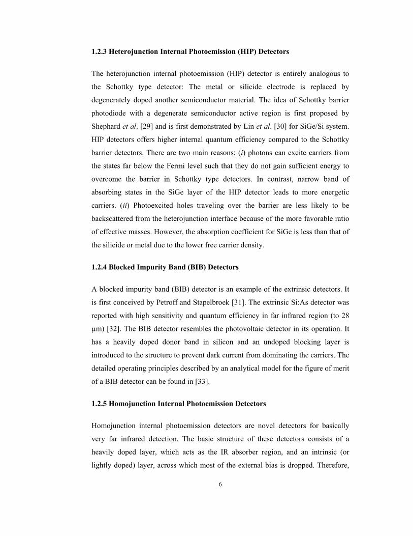
Fig. 2.13a shows the 3-dimensional representation of the variation of the yield with
respect to the effective masses ratio and the energy of the incident photons. The
projections of the 3D surface on each plane are presented in Fig. 2.13b in the
shaded form.
Fig. 2.13 a) 3-dimensional representation of the variation of the yield with respect
to the effective masses ratio and the energy of the incident photons. b) The
projections of the 3D surface on each plane in the shaded form.
The effect of different substrate (Si in this case) effective masses on the yield is
shown in Fig. 2.14. As seen in the figure, increase in the Si layer’s effective mass
causes increase in the yield as well.
2.3 Effects of Multiple Reflections and Scattering
Up to this section, we have calculated the escape probability (i.e. yield) for holes
that experience no scattering events between excitation and reaching the interface.
However, scattering affects the escape probability by redistributing the momentum
of the excited carriers: multiple reflections of the excited holes from the surfaces of
the active region as well as the collisions with phonons, imperfections and cold
electrons can either increase the yield by directing carriers into the escape volume
or decrease the yield by directing carriers out of the escape volume.
( a ) ( b )

29
0.5 1.0 1.5 2.0 2.5
0.02
0.03
0.04
0.05
0.06
0.07
0.08
m(Si) = 0.8 m0
EF + Φ = 120 meVhν = 120 meV
Yie
ld (
Vha
tche
d / V sh
ell )
M
m(Si) = 0.4 m0
Fig. 2.14 The effect of different substrate (Si in this case) effective masses on the
yield.
The scattering mechanism in such a structure junctions can be investigated in three
groups:
1. Interface scatter: (Elastic scattering) This occurs when a hot-hole interacts with
the walls of the active region (e.g. air/SiGe and SiGe/Si interfaces for Fig. 2.1) and
is not emitted.
2. Hot-hole / cold-electron scatter: (Inelastic scattering) This mechanism is
characterized by a mean free path Le and the energy loss in such an event will be so
great that the hot-hole can no longer get over the barrier.
3. Hot-hole / phonon scatter: (Semi-elastic scattering) This mechanism is
characterized by a mean free path Lp and except for collisions with cold-electrons,
all other bulk collisions such as collisions with phonons, grain boundaries, lattice
defects etc. are in this group with the mean energy loss ћω.

30
Fig. 2.15 Schematic diagram showing the different processes during the motion of
an excited carrier before emission.
The probability of reaching the barrier without colliding in the bulk for a hole
created at a distance z from the barrier is in the form exp(-z/L). L is related to the
specific scattering parameter of a hot carrier with cold electrons, phonons etc. Thus,
the accumulated probability for escape without scatter for an excited hole, which is
initially in the escape cap, can be found as (Fig.2.15-a)
∫ −−=d
LzLz dzeed
pe
0
//1α
∫ −=d
Lz dzed 0
*/1α (2.22)
Notice that (1/d) term comes from the normalization where d is the thickness of the
film. In addition to this, uniform absorption is assumed. For small photon energies,
all states in the escape volume have momentum directed approximately normal to
the barrier, and therefore, Eq. (2.22) can be written as ( ) dLe Ld /*1 */−−=α .
Air Active Region Substrate
z
d
(a)
Air Active Region Substrate
(b)
Air Active Region Substrate
(c)

31
However, for higher photon energies, the momentum component of the excited
carrier parallel to the interface increases the distance that the carrier must travel
before reaching the interface, and d in Eq. (2.22) must be replaced with d/cos(θ).
For an excited hole, the probability of escape without being scattered can then be
written as
∫ ∫ −=d
dzdLzd 0
2/
0
sin)cos*/exp(1 π
θθθα (2.23)
If the holes are not initially in the escape cap, the accumulated probability of
reaching one of the interfaces is given by (Fig.2.15-b)
∫ ∫ −−=d
dzdLzdd 0
2/
0
sin)cos*/)(exp(1 π
θθθβ (2.23)
For multiple reflections, one can similarly calculate the probability δ that a hole,
which is diffusely scattered off one surface, reaches the other surface without any
collision as (Fig.2.15-c)
∫ −=2/
0
sin)cos*/exp(π
θθθδ dLd (2.24)
And now it is easy to calculate the total accumulated probability that a hot-hole will
be emitted without colliding in the bulk. The probability that a hot-hole reaches the
barrier prior to any collision in the bulk (Y0) contains infinite number of terms
including the effects of multiple scatters off the interfaces. For example,
YF ·α (2.25)
is the probability that a hot-hole is initially in the escape cap and that it is able to
reach the barrier (see Fig.2.15-a).
YF β e-d/L* (2.26)

32
corresponds the probability that the hot-hole is initially directed toward the
air/active region interface, is scattered into escape cap at the interface and is able to
reach the barrier (see Fig.2.15-b).
If η is the probability that a hot-hole is not initially in the escape cap then the
capture probability of it which has two scatters at the interfaces with the term
considering hole which was initially directed toward the junction can be written as
YF η β δ e-d/L* (2.27)
And if this hole is initially directed to the back interface then probability becomes
YF η β δ2 e-d/L* (2.28)
In this way infinite number of terms can be written and consequently the sum of
these terms (that is Eq. (2.37-40)) will give
( )L++++++= − 42322*/0 1 δηδηηδηδβα Ld
FFi eYYY (2.29)
The term η may also be viewed as a counting loss correction term reflecting the
number of times the carrier is scattered back from the barrier before ultimate
capture and be written as
−=
∞Y
YF21η (2.30)
Where Y∞, the maximum quantum yield, is given by the volume ratio of the
spherical shell (not hatched volume in Fig. 2.6) of potentially capturable holes to
the shell of excitation (see Fig.2.16).

33
( ) ( )
( )
( ) ( )
( ) ( )
−+
Φ+−+
−+
Φ+−+
==∞
31
2
1
2/32/3
2/32/3
2/32/3
2/32/3
case
casehhE
EhE
caseEhE
EhE
V
VY
F
FF
FF
FF
excitationofshell
emissionofshell
νν
ν
ν
ν
(2.31)
Notice that the yield and hence this probability has been normalized since only a
portion of the excited states can potentially emit, and the population of the states
which can emit is depleted, while that of the non-emitting states remains
statistically unchanged.
Substituting Eq. (2.30) to (2.29) and simplifying it, Eq. (2.29) can be reduced to
( )
( )
−−
−++=
∞
∞−
2
*/0
/211
/211
δ
δβα
YY
YYeYY
F
FLdFi (2.32)
Fig. 2.16 Diagram illustrating the definition of the spherical shell of emission.
k(EF+hν)
Spherical shell of excitation
Spherical shell of emission
k2
k1
k1 k2
Case1: k(EF) k(EF+Φ)
Case2: k(hν) k(EF+Φ)
Case3: k(hν) k(hν)
34
2.4 Quantum Mechanical Effects
After the hot-hole reaches the barrier there is a finite probability that it will be
reflected at the barrier even though it is in the escape volume. If the probability that
a hot-hole in the escape volume is transmitted across the barrier is τ, then the total
yield for no collisions in the bulk is given by [62]
[ ( ) ( ) ( ) ] L+++−−+= − 222*/00 1111 δηηδηδττ Ld
i eYY
( ) ( ) ( )[ ] [ ] LL +++++−−+ − 32222*/ 111 δηηδηδτ Lde
( ) ( )2
*/0
1
111
ηδ
ηδττ
−
−−−
= − Ldi
eY
(2.33)
The first term of the above equation (i.e. Yi0τ) generates the probability of emission
without a quantum-mechanical reflection at the interface. The other terms comes
from the probability of the possible future scenarios of the subset of hot-holes
which approach the barrier with the requisite escape condition, i.e. would be
captured in the classical model, but were quantum-mechanically reflected away
from the interface uniformly in all directions.
2.5 Effect of e-p Collisions and Energy Losses
In the above sections, contributions of the scattering mechanisms to the yield have
been taken into account, however, that of the phonon collisions and hence energy
losses have not been incorporated. When this is done, the yield is viewed as a sum
of partial yields, where the nth partial yield represents the yield of the hot-holes that
have suffered n phonon collisions. This means that hot-holes are divided into
groups distinguished from each other by the number of phonon collisions. In terms
of the geometry (see Fig.2.16), as the carriers lose energy, the spherical shell of
excitation shrinks from outside to in for case1. Additionally, the inner sphere gets
smaller as well for other cases but since the effect of the reduction in hν to the

35
volume of the excitation shell is more prominent than that, the shell of excitation
shrinks.
And now, it is necessary to find the probability γ that a hole will collide with a
phonon before it collides with a cold-electron because this process leaves a hot-hole
unable to overcome the barrier. The fraction γ can be calculated as follows:
The fraction undergoing a phonon collision over a path length dz, having traveled a
total path length z, would be
p
Lz
L
dze */− (2.34)
of these, only exp(-z/Le) would not have collided on the way with a cold electron
and been removed from the process. Thus, one finds
∫∞
−−
+==
0
//
pe
e
p
LezLz
LL
L
L
dzee pγ (2.35)
At this point, the yield including contribution of successive phonon distributions
can be found by combining Eq. (2.31-33), and (2.35);
L+
−
−+
−+=
∞∞∞
2210
10
0 111 YY
Y
Y
YY
Y
YYY γγ (2.36)
where the effects of holes which have been emitted on previous distribution are
appeared in terms like (1-Yn/Y∞). And Yn (appropriate for the nth phonon
distribution) is the generalization of Eq. (2.33).
One can find Yn by upgrading the Eq. (2.15), (2.17) and (2.20) for all three cases; if
nћω is the energy loss for nth phonon distribution, (hν-nћω) is used instead of hν in
the numerator of these equations because the numerator corresponds to the escape
volume. Thus YFn can be found for M ≠ 1

36
( ) ( ) [ ]( ) ( )[ ]
( ) ( ) [ ]( ) ( )[ ]
[ ] [ ]( ) ( )[ ]
−+−
Φ+−−−−Φ+−−−+
−+−
Φ+−−−+Φ+−−+−
−+−
Φ+−−−+Φ+−−+−
=
3)1(2
)()1()()1(
2
1
2)1(2
)()1()1(
1)1(2
)()1()1(
2/32/3
2/32/3
2/32/3
2/32/32/3
2/32/3
2/32/32/3
casehhEM
MnhMMEMnhME
casehhEM
MnhMEEMnhEM
caseEhEM
MnhMEEMnhEM
Y
F
FF
F
FFF
FF
FFF
Fn
νν
ωνων
νν
ωνων
ν
ωνων
hh
hh
hh
(2.37a)
and for M = 1,
( ) ( )
( ) ( )[ ]
( ) ( )
( ) ( )[ ]
−+
Φ+−−+
−+
Φ+−−+
=
32
1
22
12
2/32/3
2/32/3
2/32/3
2/32/3
case
casehhE
EnhE
caseEhE
EnhE
YF
FF
FF
FF
Fn
νν
ων
ν
ων
h
h
(2.37b)
Eq. (2.37) and/or (2.38) can then be used in Eq. (2.33) to generate ultimate yield Yn.
The series is truncated when “thermalization” occurs, i.e.
ν
ν
h
hn
Φ−=max (2.38)
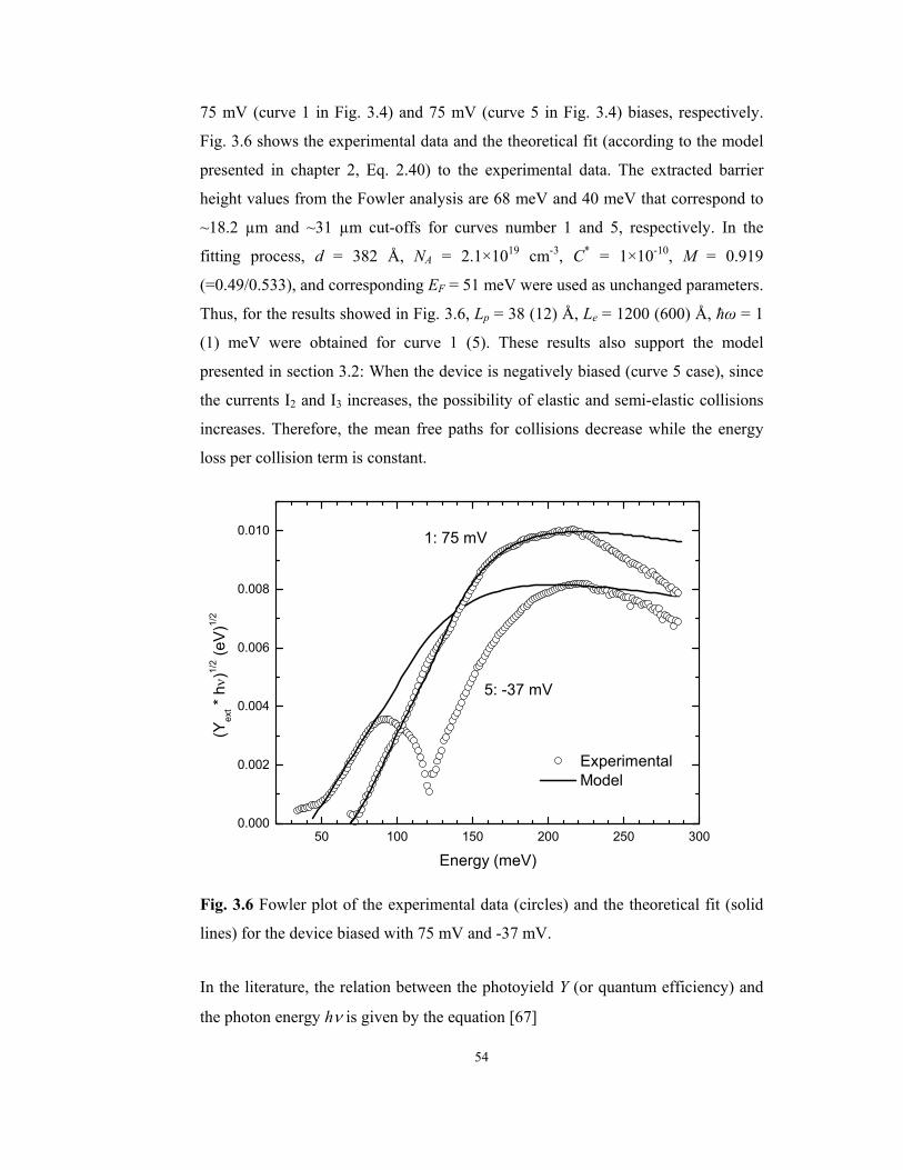
37
2.6 Analysis: Effects of the Scattering Parameters on the Yield
In this section the results of the model developed above will be given by a series of
graphs. For the calculations, all equations have been used as in the original form
presented in the thesis; no approximations have been made except that the quantum
mechanical transmission probability was taken to be τ = 1. It can also be noted that
since the model presented here does not include the temperature dependence, it can
be thought that the device is operated at 0 K. In fact, for the model developed for
the PtSi/Si Schottky type infrared photodetectors, we had the conclusion that the
internal photoemission is expected to be almost temperature independent [70].
Unless otherwise stated, Φ = 40 meV, EF = 80 meV, m1 = 0.751 m0 (corresponding
to the Fermi level used, from reference [69]), and m2 = 0.522 m0 have been used in
the calculations. These values are close to the ones for a p-type highly doped
SiGe/Si HIP operating for the mid-infrared region.
Fig. 2.17 shows the yield calculated from the Eq. (2.36) for different layer
thicknesses with the following parameters: Lp = 50 Å, Le = 1000 Å and ћω = 1
meV. Note that it is hard to estimate and/or measure these parameters; the ones used
here are within the ranges suggested by Mooney and Silverman [61,62] for
Schottky IR technology (Lp ≈ 50-150 Å, Le ≈ 500-5000 Å and ћω ≈ 1-10 meV).
Strong et al. [65] used similar values for Le and Lp for their SiGe/Si detectors; they
extracted the elastic scattering length Lp of 10 Å from the relaxation time
measurements in heavily doped material.
The upward curvature of the theoretical curves for low photon energies in the graph
can be explained as follows: As the energy of the incident photon increases, the hot-
hole can survive for more phonon collisions and have more chance to be redirected
to the escape volume. But for higher photon energies, since the elimination of the
previously emitted carriers becomes pronounced, the curves start to roll off from the
linearity. So, one can say that this is more significant for the lower energy loss term
(see Fig. 2.20 as well). Since the yield around the barrier height is quite small, in
Fig. 2.17 the cut-off energy of the system looks like 50 meV although it is 40 meV.
If the graph had been plotted in logarithmic scale, it would be seen that the cut-off

38
energy is what it should be. The effect of the film thickness can also be seen in Fig.
2.17. Decrease in the thickness of the active region causes an increase in the number
of wall scattering and hence hot-holes are redirected to the escape volume.
Therefore, the yield increases.
50 100 150 200 250 3000.0
0.1
0.2
0.3
0.4
0.5
0.6
0.7
d=400 A
d=200 A
d=100 A
Yiel
d
hν (meV)
EF=80 meVΦ =40 meVLe=1000 ALp=50 Ahw=1 meV
d=50 A
Fig. 2.17 Effect of the film thicknesses on the yield versus energy plots.
Fig. 2.18a and 2.18b show the effects of the different Lp values on the yield for ћω
= 1 meV and ћω = 10 meV respectively. As seen here, the effect of the variation in
the mean free path for semi-elastic collisions depends on the excitation energy, film
thickness, and the energy loss value per collision. For low excitation energies, few
phonon collisions suffice to thermalize the carrier, so shorter Lp values lead to lower
yield. This effect is more pronounced for high energy loss case (Fig. 2.18b). On the
other hand, at high excitation energies, the hot-hole is less easily thermalized and
more probably redirected into the escape direction and hence phonon scattering
tends to increase the yield for the small energy loss case (Fig. 2.18a).
In Fig. 2.19 Le dependence of the yield is demonstrated. For a hot-hole, small mean
free path of elastic collisions means high probability of collision with a cold-
electron.

39
50 100 150 200 250 3000.0
0.1
0.2
0.3
0.4
0.5
Lp=1000 A
Lp=100 Ad=100 AEF=80 meVΦ =40 meVLe=1000 Ahw=1 meV
Yiel
d
hν (meV)
Lp=10 A
( a )
50 100 150 200 250 3000.0
0.1
0.2
0.3
0.4
0.5
( b )
d=100 AEF=80 meVΦ =40 meVLe=1000 Ahw=10 meV
Yiel
d
hν (meV)
Lp=100 A
Lp=1000 A
Lp=10 A
Fig. 2.18 Yield versus energy plots for several hot-hole/phonon scattering mean
free paths (Lp) with an energy loss per collision (ћω) of a) 1 meV, and b) 10 meV.

40
Therefore, due to the fact that energy loss in hot-hole/cold-electron scattering is
very big, the hot-hole can no longer get over the barrier. So, the yield reduces
dramatically with decreasing Le value.
50 100 150 200 250 3000.0
0.1
0.2
0.3
0.4
0.5
0.6
0.7
0.8
Le=5000 A
Le=1000 A
d =100 AEF=80 meVΦ =40 meVLp=50 Ahw=1 meV
Yie
ld
hν (meV)
Le=100 A
Fig. 2.19 Yield versus energy plots for several hot-hole/cold electron scattering
mean free paths (Le).
Fig. 2.20 shows the effect of the energy loss term on the yield. As we mentioned
above when describing the other graphs, when the energy loss per collision
decreases, carriers’ chance to fall in the escape volume increases. Therefore, one
can see the yield increases with a given excitation energy. This increase in the yield
reduces for high photon energies because of the elimination of the previously
emitted carriers. This is the explanation for the roll off at high energies in the
graphs.
Effect of the Fermi level position in the active region to the yield is shown in Fig.
2.21. For the constant barrier height, there will be no change in the number of
excited carriers as the Fermi energy decreases. They, however, will have relatively
high energy and thus have more chance to be redirected into the escape volume

41
before collisions will thermalize the carriers. So, the yield increases with decreasing
Fermi level.
50 100 150 200 250 3000.0
0.1
0.2
0.3
0.4
0.5
hw=10 meV
hw=5 meV
d =100 AEF=80 meVΦ =40 meVLe=1000 ALp=50 A
Yiel
d
hν (meV)
hw=1 meV
Fig. 2.20 Effect of the energy loss per collisions (ћω) term on the yield.
50 100 150 200 250 3000.0
0.1
0.2
0.3
0.4
0.5
0.6
0.7
EF=80 meV
EF=60 meV
d =100 AΦ =40 meVLe=1000 ALp=50 Ahw=1 meV
Yiel
d
hν (meV)
EF=40 meV
Fig. 2.21 Yield versus energy plots for different Fermi energies.

42
Finally, Fig. 2.22 shows the variation of the yield for different barrier height values.
For constant Fermi level, when the barrier height gets smaller, there will be net
increase in the number of carriers that can overcome the barrier. They can also be
counted as relatively high energetic carriers. As a result, the yield increases with
decreasing barrier height and the curves shift without changing their features.
50 100 150 200 250 3000.0
0.1
0.2
0.3
0.4
0.5
Φ =100 meV
Φ =60 meV
d=100 AEF=80 meVLe=1000 ALp=50 Ahw=1 meV
Yiel
d
hν (meV)
Φ =20 meV
Fig. 2.22 Variation of the yield with different barrier height values.
2.7 Infrared Absorption
As it is stated at the beginning of this chapter, external yield is defined as the
product of the optical absorption and the internal yield calculated above.
Experiments showed that the incoming photons are absorbed in the film via free-
carrier absorption [68,71,72]. Classically, free-carrier absorption results from the
damped motion of carriers which are accelerated in the direction of the photon
electric field (i.e. parallel to the wafer surface with normally incident illumination).
The absorption coefficient (in cm-1 unit) is given [73]

43
τπ
λα
32
22
8 ncm
qN A
∗= (2.39)
where NA is the doping concentration, q is the electronic charge, λ and n are
respectively the wavelength of the incident photon and the index of refraction, m* is
the effective mass of the active region, c is the speed of light and τ is the relaxation
time that reflects the influence of the scatterers. Since the optical absorption is the
defined as the product of the absorption coefficient α and the film thickness d, then
the external yield can be written as
( ) int2 YCdNY Aext λ∗= (2.40)
where C* is the collection of constant terms such as effective mass, optical
constants, speed of light, etc. It is an unitless parameter whose order is around 10-10.
Fig. 2.23a shows the external yield versus photon’s energy graph; the difference
both in magnitude and shape can be easily seen when compared to the previous
graphs (e.g. Fig. 2.17). Low yield values in the high energy part of the graph come
from the wavelength dependent feature of the absorption process (Eq. (2.39)). In the
calculations of the external yield, the following values were used for the
parameters; Φ = 40 meV, EF = 80 meV, d = 100 Å, Lp = 50 Å, Le = 1000 Å, ћω = 1
meV, NA = 5×1019 cm-3 and C* = 1×10⁻¹⁰. In Fig. 2.23b, same graph have been
plotted in the form of Fowler plot since it is the traditional way of presenting the
results.
In the analysis of our experimental results, this final form of the model was used
and a good agreement was seen. Details of this analysis are given in chapter 3 and
partly in chapter 4.
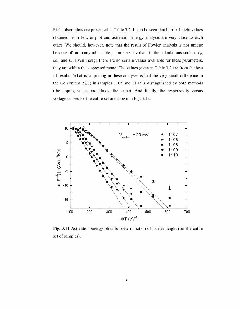
44
50 100 150 200 250 3000.0
2.0x10⁻⁴
4.0x10⁻⁴
6.0x10⁻⁴
8.0x10⁻⁴
1.0x10⁻³
EF=80 meVΦ =40 meVLe=1000 ALp=50 Ad=100 Ahw=1 meVNA=5x10¹⁹ (cm-3)
C*=10-10
Ext
erna
l Yie
ld
hν (meV)
( a )
50 100 150 200 250 3000.000
0.002
0.004
0.006
0.008
0.010
0.012
( b )
EF=80 meVΦ =40 meVLe=1000 ALp=50 Ad=100 Ahw=1 meVNA=5x10¹⁹ (cm-3)
C*=10-10
(Yex
t hν)
1/2
hν (meV)
Fig. 2.23 a) External yield (product of the internal yield and the optical absorption)
versus energy plot, b) same graph in the form of Fowler plot.

45
CHAPTER 3
MECHANISMS OF PHOTOCURRENT GENERATION IN SiGe/Si HIP
INFRARED PHOTODETECTORS
Si1-xGex/Si heterojunction internal photoemission (HIP) infrared photodetectors
have attracted a lot of interest in recent years [30,63,64,65,72,74,75]: Their cut-off
wavelength adjustability over a wide infrared range, relatively high quantum
efficiency at longer wavelength compared to silicide Schottky barrier detectors, and
the compatibility with the existing Si technology make them attractive. The
operation mechanism of the SiGe/Si heterojunction infrared photodetector is the
same as that of the PtSi/Si Schottky barrier detector (discussed in chapter 5), which
is the most popular and studied Schottky barrier detector [61,76]. The incident
infrared radiation is absorbed via free carrier absorption in heavily doped Si1-xGex
layer and followed by the internal photoemission of photo-excited holes over the
SiGe/Si heterojunction barrier into the Si collector layer. The cut-off wavelength λc
of the HIP detector is determined by the effective barrier height Φ which is the
energy difference between the Si1-xGex/Si valence band offset ∆Ev and the Fermi
level EF in the Si1-xGex layer. Thus, the cut-off wavelength of a SiGe/Si HIP
detector can be tailored over a wide infrared range by engineering the Ge content
and the doping concentration of the Si1-xGex layer.
The study on the mechanisms of the photocurrent generation can help us to obtain a
clear physical understanding of the device operation. Although there have been
many papers published on the detection mechanisms of HIPs, we feel that the basic
current mechanisms have not been adequately addressed and clearly resolved. In

46
this chapter, physical effects governing the photocurrent generation process is
studied, and therefore, the devices used here are not expected to have best
performance for practical applications. As a matter of fact, for example, the
responsivity values of our devices are less than that of similar ones. On the other
hand, interesting experimental results were observed, such that they can be labeled
as a “voltage tunable” infrared photodetector. Among infrared detector studies,
multispectral detection and/or tunable cut-off wavelength properties have been paid
special attention [34,36,77-81]. Schottky barrier [78], metal(silicide)-
semiconductor-metal(silicide) [79,80], homojunction IPs [34,36], and especially
quantum well structures [81, and references therein] have been the subject of these
studies in recent years. In this chapter, we present a Si1-xGex/Si with x=0.11 HIP
whose cut-off wavelength can be varied by the externally applied bias, and a
qualitative model by identifying the photocurrent generation mechanisms in the
structure to explain the experimental results. And finally, the experimental results of
a set of samples with different parameters are presented. Part of this chapter has
been published and can be found in [82].
3.1 Experimental Details and Device Operation
The samples used in this study were grown on 0.01-0.02 Ω cm Boron doped (3-
8×1018 cm-3) p-type Si (001) substrate by ultra-high-vacuum chemical vapor
deposition (UHV-CVD). Details of the growth procedure have been given
elsewhere [83]. A schematic layer structure and the valence band edge profile are
shown in Fig. 3.1. Along the growth direction, the sample consists of 100 nm
undoped Si layer, 38.2 nm p+ -Si1-xGex active layer with x = 0.11, and 5 nm p+ -Si
layer followed by a 197 nm p-Si top contact layer. Si1-xGex active layer was doped
to about 2.1×1019 cm-3 with boron to increase the amount of absorption and the top
contact layer was doped to about 6×1018 cm-3 with B to act as a reservoir of charged
carriers (holes). Layer thicknesses and the doping levels (also indicated in Fig. 1)
were determined from x-ray diffraction (XRD) and Auger electron spectroscopy
(AES). Doping levels were also verified by secondary-ion-mass-spectroscopy
(SIMS) measurements. Similar structures with different Ge alloy fractions and layer
thicknesses were also investigated and similar behaviors were observed.

47
Fig. 3.1 Schematic device structure with layer thicknesses and the valence band
edge profile showing the basic operation principle of the SiGe/Si HIP investigated
here.
Mesa devices of 400x400 and 600x600 µm2 in size were defined by wet etching,
and top and bottom ohmic contacts were made by evaporating Al followed by rapid
thermal annealing. The top Al contacts were ring shaped to allow normal incidence
illumination. Fig. 3.2 shows the schematic representation of a device: in part (a)
cross-section of the device and in part (b) the top view of the mesa with ring shaped
Al ohmic contact are shown. Width of the square-shaped ring contact is 50 µm and
the distance between the inner sides is 370 µm. For spectral photoresponse
measurements, a closed cycle helium cryostat with KBr window and a Bomem
MB100 Fourier transform infrared spectrometer with a globar source were used.
Devices were illuminated from the top opening. The responsivity calibrations were
done using a 1000-K blackbody infrared source, with the excitation wavelength
selected by a variable narrowband filter. Fig. 3.3 shows the responsivity
measurement setup.
p –Si substrate
p+ –Si0.89Ge0.11
Si
p –Si top contact
p+–Si hν
197 nm, 6×1018 cm-3
5.0 nm, 5×1019 cm-3
38.2 nm, 2.1×1019 cm-3
100 nm
3-8×1018 cm-3

48
Fig. 3.2 The schematic representation of a device: (a) cross-section of the device
and (b) the top view of the mesa with ring shaped Al ohmic contact.
Fig. 3.3 Responsivity measurement setup.
3.1.1 Device Operation
The basic device operation (see Fig. 3.1) relies on the absorption (through free-
carrier absorption) of the long wavelength infrared (LWIR) photons in a p-type
heavily doped SiGe layer, followed by the collection of the photoexcited holes (i.e.
internal photoemission) over the potential barrier formed by the SiGe-Si valence
band offset, as demonstrated by Lin et al [30,84]. Our device design (Fig. 3.1),
p+-Si substrate
p+-Si top-contact
Al ohmic ring
contacts
p+-Si top-contact
( a ) ( b )
Load Resistance
chopper filter
lens
Sample/cryostat
Lock-in amplifier
Source measurement unit
BB source

49
which is first proposed by Liu et al [64], is similar but with some modifications for
easier growth and fabrication. The undoped silicon layer forms a triangular barrier.
Si1-xGex active layer, which is doped heavily to enhance infrared absorption, is thick
enough to ensure free carrier absorption and thin enough to increase the effect of
multiple traversals through the SiGe film walls. To reduce the resistance from the
heterojunction between SiGe and the p-Si layers (top contact) a heavily doped Si
layer is added. The same structure with thin undoped SiGe layer inserted between i-
Si and SiGe active layer has been used as a double-heterojunction Si-SiGe-Si
unipolar transistor by fabricating a three terminal device [85].
Cut-off wavelength of our devices, unlike other HIPs in the literature having only
SiGe/Si junction, have strong dependence on the applied bias. The voltage
dependence of the photoresponse [86] and the quantum efficiency [66] have been
presented before (in the literature) but this does not necessarily mean that the cut-
off wavelength of the detector also depends on the voltage across the device. All
SiGe/Si photodetectors, whose cut-offs change with the applied bias and showing
the similar experimental results with ours, have a metal or a silicide layer to shape
the potential barrier [35,77,79,87]. For the particular sample presented here, we
obtained cut-off wavelength that can be tailored between 31 µm and 18.2 µm by
changing the potential difference across the device. From the working region point
of view, our devices can be compared with the Si based blocked impurity band
(BIB) detectors even though the responsivity values obtained here are much less
then that of BIB detectors [88-90]. Moreover, the structure presented here is
superior to the BIB detectors in terms of the cut-off wavelength tunability.
3.2 Spectral Photoresponse and a Simple Model
Fig. 3.4 shows the spectral photoresponse curves for the SiGe sample under
different potential differences across the device at 10 K. All voltage polarities are
defined with respect to the bottom contact, i.e., the positive bias is defined as the
top of the mesa biased positively with respect to the bottom. As seen in the figure,
despite that the applied bias values are very small, dramatic changes were observed
in the photoresponse of the device. When it is under illumination, the device has

50
5 10 15 20 250
4
8
12
16
-50 0 50 100 150-10
-5
0
5
10
15
20
25
30
Pho
tore
spon
se (a
u)
Wavelength (µm)
1
2
3
4
5
1: 75 mV2: 20 mV3: -10 mV4: -24 mV5: -37 mV
Applied bias (mV)
∆V
(mV
)
15
10 K
Fig. 3.4 Spectral photoresponse curves under different bias conditions at 10 K. The
voltage values written in the legend are the potential differences across the device
when it is illuminated by the light coming from the IR source. The inset shows the
change in the photovoltage with the applied bias for 10 K measurements.
-37 mV offset voltage across its terminals and shows double peak feature in the
photoresponse spectrum. As the device biased positively, the second peak appearing
in the longer wavelength region of the spectrum starts to disappear while the first
one becomes prominent. The first peak position shifts from ~6.5 µm to ~7.7 µm
with the applied voltage whereas the second peak position remains unchanged. Note
that the voltage values written in the legend are the potential difference values
across the device when it is illuminated by the light coming from the IR source. The
device has shown photovoltaic behavior. The inset in Fig. 3.4 shows the graph of
the photovoltage, ∆V, versus applied bias for 10 K measurements. As shown here,
as the applied bias is increased in positive direction, the photovoltage increases with
decreasing increments. This means that the photocurrent produced in the structure
increases with the applied bias and becomes almost constant at high voltages.
Therefore, it can be concluded that there are other current mechanisms apart from
the internal photoemission process in the structure or the internal photoemission is

51
somehow affected by the applied bias indirectly. The decrease in the final data is
artificial because at that bias, it is difficult to sift the photocurrent due to the high
dark current.
To interpret the observed results, we use the qualitative picture shown in Fig. 3.5.
Under illumination, multiple photocurrents in opposite directions are generated in
the structure: I1 and I2 are created by the photons absorbed in the SiGe well and
directed towards the bottom contact and top contact, respectively. I3 and I4 are the
photocurrents formed by the hot holes generated in the bottom and the top contact
layers, respectively. The absorption in these layers together with the barriers leads
to a net photocurrent. Depending on the p+ -Si layer thickness and the device
operating temperature, effects of the currents I2 and I4 to the net photocurrent can be
significant. The model described here takes all possible current mechanisms into
account. Due to different spectral responses and different positions along the light
propagation path, their competition gives distinct outcomes in different spectral
regions. As seen in Fig. 3.4, the second peak is not as strong (dominant) as the first
one because most of the incident light is absorbed in the SiGe well before they
reach the bottom contact and the absorption in p-Si region is not as high as that of in
the SiGe region since the doping level is relatively low. According to this picture,
I1 and I4 are responsible for the first peak while I2 and I3 are responsible for the
second one. When the device is negatively biased, V < 0, valence band edge bends
as shown in Fig. 3.5a. Therefore, the amount of current flowing towards the top
contact (reverse direction) increases when compared to the equilibrium position, V
= 0, and becomes comparable with the main current. Note that, at equilibrium there
is a net photocurrent in the forward direction (towards the bottom contact) as
considered in HIPs. We now discuss the reason of increase in the reverse current
under negative bias: If the tunneling process from the SiGe/i-Si barrier is neglected,
it can be said that I1, the main current, is independent of applied bias, so it is
constant. Due to the very thin barrier between the p+ -Si and SiGe layers and the
low operating temperature, the tunneling process can not be neglected for I2,
therefore, it increases. I3 increases, too, because the apparent barrier for the carriers
in reverse direction is reduced. As for I4, since the generated holes see higher barrier

52
Fig. 3.5 Qualitative physical picture for interpreting the experimental results. The
potential difference is negative for (a) and positive for (b). The bottom contact is the
ground and arrows show the direction of the photoexcited holes’ direction.
it decreases. Consequently, net current in the reverse direction increases with
increasing reverse bias. In negative bias condition, since the potential barriers for
the second and the third current mechanisms are less than that for the others, they
show themselves in the long wavelength part of the spectrum. Thus, this second
peak screens the main peak and therefore causes an artificial shift in the peak
position as well as the decrease in the response as seen in Fig. 3.4. Moreover, since
the cut-off wavelength of the device is determined by the smallest distinguishable
barrier, the tale of the second peak stretch out in the longer wavelength as the
potential difference across the device increase in the reverse direction. This feature
is also clear in Fig. 3.4. On the other hand, when the device is biased positively, V >
0, band edge profile becomes as shown in Fig. 3.5b. In a similar approach with the
(a)
(b)
Top contact layer
Bottom contact layer
SiGe active layer
I4 I2 I1 I3
EV
EF
EV
EF

53
above discussion, the suppression of the reverse current and the increase in the net
current in the forward direction can easily be explained. Briefly, the decrease in the
tunneling probability for I2, the increase in the potential barrier for I3, and the
decrease in the potential barrier for I4 are responsible for this feature.
If the above qualitative interpretation is correct, we would expect a temperature
change to simulate the effect shown in Fig. 3.4: The effect of the voltage increase
(in the forward direction, i.e. from 5 to 1 in the Fig. 3.4) on the creek position
should be similar to that of the temperature increase when the potential difference
across the device under illumination is the same. But we would not expect the same
increase in the response as in the figure. On the contrary, one can expect decline in
the peak value because of the increase in the dark current. We then plotted the
photoresponse versus wavelength graph (not shown here) for temperatures 10 K, 20
K and 30 K when V = -10 mV, and saw the same red shift in the creek’s position.
Additionally, it also met with the expectation of decrease in the maximum response
value for higher temperatures. The effect of the temperature on the photoresponse
curves of our devices when they are biased to obtain maximum signal can be found
in the following chapter.
3.2.1 Fowler Analysis
As a result, our device acts as an infrared photodetector whose cut-off wavelength
can be adjusted by applying different potential differences across the device. In
order to demonstrate the change of cut-off wavelength with applied bias for this
sample, the measured photoresponse data were converted to Fowler plots. Since the
yield (or the quantum efficiency) can be written as the product of the responsivity
(A/W) and the photon energy (eV), photoresponse data of the device (Fig. 3.4) were
multiplied by a calibration constant in a way that the photoresponse value
corresponding with the wavelength at which the responsivity measurement was
performed will be the responsivity value obtained for that wavelength. Details of
the responsivity measurements are given in section 3.3. For the conversion, we used
the responsivity value obtained for the bias at which the spectral photoresponse
measurements were done (see Fig. 3.7); 2.1 mA/W and 1.1 mA/W at 7.14 µm for

54
75 mV (curve 1 in Fig. 3.4) and 75 mV (curve 5 in Fig. 3.4) biases, respectively.
Fig. 3.6 shows the experimental data and the theoretical fit (according to the model
presented in chapter 2, Eq. 2.40) to the experimental data. The extracted barrier
height values from the Fowler analysis are 68 meV and 40 meV that correspond to
~18.2 µm and ~31 µm cut-offs for curves number 1 and 5, respectively. In the
fitting process, d = 382 Å, NA = 2.1×1019 cm-3, C* = 1×10⁻¹⁰, M = 0.919
(=0.49/0.533), and corresponding EF = 51 meV were used as unchanged parameters.
Thus, for the results showed in Fig. 3.6, Lp = 38 (12) Å, Le = 1200 (600) Å, ћω = 1
(1) meV were obtained for curve 1 (5). These results also support the model
presented in section 3.2: When the device is negatively biased (curve 5 case), since
the currents I2 and I3 increases, the possibility of elastic and semi-elastic collisions
increases. Therefore, the mean free paths for collisions decrease while the energy
loss per collision term is constant.
50 100 150 200 250 3000.000
0.002
0.004
0.006
0.008
0.010
Experimental Model
(Yex
t * hν)
1/2 (e
V)1/
2
Energy (meV)
1: 75 mV
5: -37 mV
Fig. 3.6 Fowler plot of the experimental data (circles) and the theoretical fit (solid
lines) for the device biased with 75 mV and -37 mV.
In the literature, the relation between the photoyield Y (or quantum efficiency) and
the photon energy hν is given by the equation [67]

55
ν
ν
h
hCY
2
1
)( Φ−= (3.1)
because of the simplicity. Here 1C is the emission coefficient depending on the
absorptance and the Fermi energy level in the SiGe active region. In fact, Eq. (3.1)
is the approximated form of the Eq. (2.15) (Φ < hν << EF), and does not include the
scattering effects. Experimental data in Fig. 3.6 were also analyzed with this
equation in order to show the differences between this model and the model
presented in chapter 2. From Eq. (3.1), we obtained 17.8 µm and 28.3 µm cut-offs
for curves number 1 and 5, respectively. As seen here, it then overestimates the
barrier height of the junction.
3.3 Responsivity versus Voltage
The responsivity versus voltage characteristics of the device at different
temperatures are shown in Fig. 3.7. Measurements were performed at the peak
position of the spectral photoresponse curve, i.e. at 7.14 µm (see Fig. 3.4). As seen
in the figure, responsivity of the device showed strange features that we do not fully
understand, nevertheless, most of them can be understood by considering the model
described in section 3.2. The general character of the curve is similar for all
temperatures; therefore, we now talk on 10 K results (voltage values that will be
given are different for different temperatures). The curve is in a complete harmony
with the inset in Fig. 3.4 for the voltage region where the spectral photoresponse
measurements have been performed, i.e., from about -50 mV to 150 mV. Change in
responsivity values has a significant dependence on the voltage up to 0 mV, since
the competition between currents is influential in that voltage range. The amount of
currents flowing in opposite directions are the same at the turning point where the
responsivity value is zero (non-zero for 30 K and 40 K because of the increase in
the noise level arising from the high dark current and/or the lack of data at which
both currents are equal). As for 0-170 mV region, responsivity is almost
independent of the applied bias as expected from a HIP detector [66,86], so we call
this region as “internal photoemission region”. However, at ~145 mV, there is a
jump in the values and the graph makes a nick that we could not explain with a
56
negative slope. As the temperature increases, the nick’s slope gets smaller and it
covers a larger region. Starting from ~180 mV the increase can be attributed to the
hole injection from the top to the SiGe layer, i.e., a nonequilibrium hole distribution
is created in the center region (see Fig. 3.5b) [85,91]. Therefore, the hole current
from the SiGe region to the bottom increases since the absorption in this region
increases, too. Finally, the effect of the temperature to the graph can be explained as
follows: Since the reverse currents (I2 and I3) are suppressed as the temperature
increases, the main current mechanisms (basically I1, and I4) become dominant.
Thus, the effect of the high voltage for the low temperature can be achieved with
lower voltage at high temperature. As a result, all features seen in Fig. 3.7 (such as
shift in zero point crossing and the position of the nick, etc) shift towards the small
voltage region in the graph as the temperature goes up. Indeed, this is what we
observed in the spectral photoresponse measurements at higher temperatures.
-0.15 -0.10 -0.05 0.00 0.05 0.10 0.15 0.20 0.250.000
0.001
0.002
0.003
0.004
0.005
0.006
0.007
@ 7.14 µm
Res
pons
ivity
(A/W
)
Voltage (V)
10 K 20 K 20 K 40 K
Fig. 3.7 Responsivity versus voltage characteristics of the device at different
temperatures. Measurements have been performed at 7.14 µm.

57
For the sake of completeness, detectivity D* values were obtained by using shot
noise approximation. Since we could not read the dark current values below 100 pA
due to the electrical noise limit of the measurement setup, the peak value of the
detectivity was estimated; it is in the order of 1012 cm Hz1/2 /W. This value is less
than that of BIB detectors [88,89], but higher than SiGe HIP detectors’ detectivity
values presented in the literature [65,72,74].
3.4 I-V Characteristics and Activation Energy Analysis
To understand the carrier transport through the structure, I-V characteristics of the
samples were studied under different experimental conditions. I-V curves of the
sample, which were obtained when it is exposed to the light coming from the
laboratory environment, are shown in Fig. 3.8. The dark current obtained at 10 K
was also plotted for comparison. The graph is completely in agreement with the
other measurements presented above. The excess current seen for low bias and
temperature values is due the photo-generated carriers at or near the barriers. This
current is composed of two components: the internal photoemission over the barrier
and the band-to-band excitation in the intrinsic Si in which an electric field is set up.
The band-to-band excitation is effective for photon energies greater than silicon
bandgap at the measurement temperature. The photocurrent is observable at low
temperatures where the dark current is suppressed sufficiently. The presence of the
potential barrier manifests itself as a step feature in the photocurrent part of the I-V
curves. Note that the voltage region where the step has been seen corresponds to the
“internal photoemission region” excluding the nick part in Fig. 3.7. This step
disappears as the temperature increases because the dark current through the barrier
junction starts to dominate the current at relatively low temperatures. The dark
current is an important issue when the device performance is considered.
It is well known that the temperature dependence of the dark current can be used to
determine the barrier height of the device by using the thermionic current equation
[92],

58
-0.15 -0.10 -0.05 0.00 0.05 0.10 0.15 0.20 0.25
1E-9
1E-8
1E-7
1E-6
1E-5
1E-4
10 K, dark
Cur
rent
(A)
Voltage (V)
10 K 20 K 30 K 40 K
Fig. 3.8 Semilogarithmic plot of I-V characteristics of the sample under different
experimental conditions.
100 200 300 400 500 600 700
-15
-10
-5
0
5
10
Ln(J
/T2 ) [
ln(A
/cm
2 K2 )]
1/kT (eV-1)
Experimental lineer fit
Vapplied = 20 mVΦeffective = 89.7 meV
Fig 3.9 Activation energy plot for determination of barrier height.

59
−Φ−= ∗
kT
qVTAAI aexp2 (3.2)
where A is the device area, A* is the Richardson constant, and Va is the applied bias.
As seen here, the slope of a plot of ln(J/T2) versus 1/kT (known as Richardson plot)
yields the activation energy (effective barrier height) Φ−qVa. Fig. 3.9 shows the
activation energy plot of the forward current (20 mV) in our device for
determination of barrier height. From the slope, 89.7 meV activation energy was
obtained, which corresponds to 69.7 meV barrier height. This value is very close to
barrier height value obtained from Fowler analysis, 68 meV. The discrepancy
between the experimental data and the solid line (linear fit) at low temperatures
comes from the fact that thermionic current is not the dominant current mechanism
at very low temperatures. This is the region in which tunneling processes become
more effective. Actually, this discrepancy for Schottky type junctions has been
studied extensively as a part of current mechanism studies. Since this point is not
within the main concern of this thesis, it is not discussed further. For more details,
see [93], and references therein.
3.5 Samples with Different Parameters
The sample discussed in above sections in fact belongs to a set of samples with
different parameters. Since each sample has the same structure and shows the same
behavior in terms of the experimental results, we found that it is convenient to
present all the results over only one of them. As in this section, details of the other
samples and the experimental results are given in a very compact form.
Table 3.1 shows the structural parameters of the samples as determined by XRD,
AES and SIMS. Note that the sample used in the previous sections is 1108. The
spectral photoresponse curves of the entire set are shown in Fig. 3.10. For these
spectrums, devices were biased with 75 mV except for sample 1105 which was
biased with 20 mV. These are the values at which maximum signal was obtained.
Besides, photoresponse values were normalized to 1 to make easy comparison
between different samples. It is seen that the cut-off wavelengths changes in a range
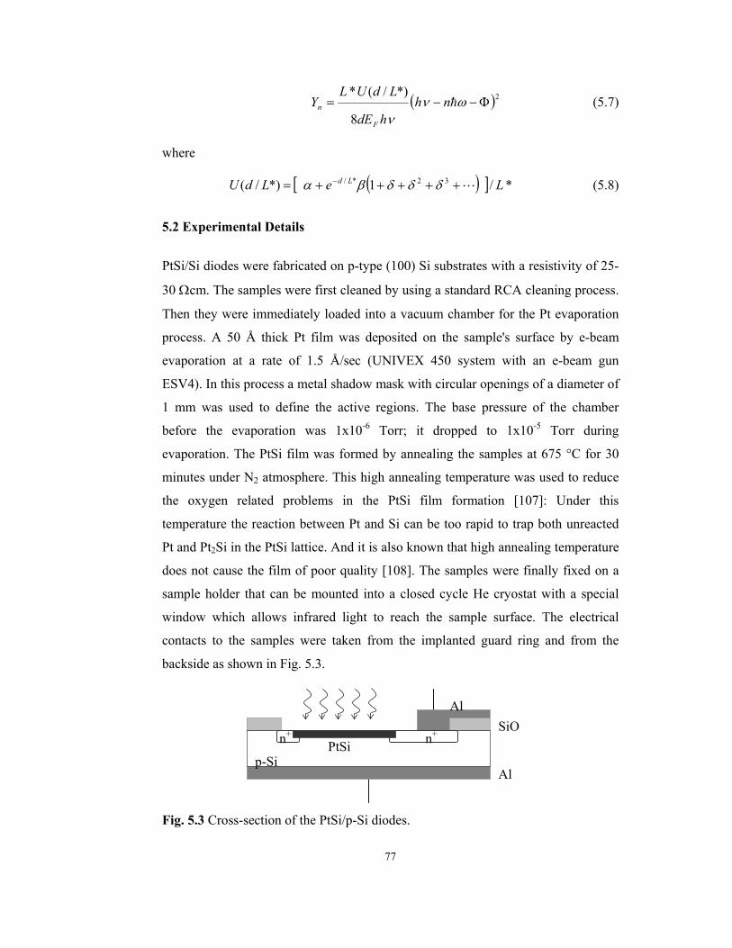
60
of ~14 µm to ~27 µm depending on the Ge content and doping amount in the SiGe
active region of that sample.
Table 3.1 Structural parameters of the samples.
Si1-xGex i-Si Si contacts
Sample Thickness (nm) x Doping
(cm-3) Thickness
(nm) Doping (cm-3)
Thickness (nm)
Doping (cm-3)
1105 16.9 0.100 1.6E19 4.2 6.3E19 188 1.7E18
1107 31.2 0.093 1.5E19 4.0 4.5E19 201 6.0E18
1108 38.2 0.110 2.1E19 5.0 5.0E19 197 6.0E18
1109 18.9 0.135 2.5E19 4.0 3.3E19 198 4.5E18
1110 11.6 0.132 2.0E19 4.8 2.7E19 198 5.5E18
5 10 15 20 250.0
0.2
0.4
0.6
0.8
1.0
Pho
tore
spon
se (n
orm
aliz
ed)
Wavelength (µm)
10 K
1105
1107
1108
1109
1110
Fig 3.10 Spectral photoresponse curves for a set of samples. Samples were biased
with 75 mV except 1105 which is biased with 20 mV.
Fowler and activation energy analysis also confirm the order in Fig.3.10. The
Richardson plot for all the samples can be seen in Fig. 3.11. Parameters used in
Fowler analysis and the extracted barrier height values both from Fowler and

61
Richardson plots are presented in Table 3.2. It can be seen that barrier height values
obtained from Fowler plot and activation energy analysis are very close to each
other. We should, however, note that the result of Fowler analysis is not unique
because of too many adjustable parameters involved in the calculations such as Lp,
ћω, and Le. Even though there are no certain values available for these parameters,
they are within the suggested range. The values given in Table 3.2 are from the best
fit results. What is surprising in these analyses is that the very small difference in
the Ge content (‰7) in samples 1105 and 1107 is distinguished by both methods
(the doping values are almost the same). And finally, the responsivity versus
voltage curves for the entire set are shown in Fig. 3.12.
100 200 300 400 500 600 700
-15
-10
-5
0
5
10
Ln(J
/T2 ) [
ln(A
/cm
2 K2 )]
1/kT (eV-1)
1107 1105 1108 1109 1110
Vapplied = 20 mV
Fig. 3.11 Activation energy plots for determination of barrier height (for the entire
set of samples).

62
Table 3.2 Parameters used in Fowler analysis and the barrier height values obtained
from both electrical and optical measurements.
Sample 1105 1107 1108 1109 1110
M 0.974 0.978 0.919 0.959 1.010
C* 1E-10 1E-10 1E-10 1E-10 1E-10
EF (meV) 44 43 51 58 53
Lp (Å) 50 60 38 40 75
Le (Å) 4200 2000 1200 1550 4000
ћω (meV) 2 2 1 1 2
ΦFowler (meV) 52 46 68 75 86
ΦAct. (meV) 49.9 45.4 69.7 79.1 88.4
-0.15 -0.10 -0.05 0.00 0.05 0.10 0.15 0.20 0.25 0.30 0.350.000
0.002
0.004
0.006
0.008
0.010
Res
pons
ivity
(A/W
)
Voltage (V)
1105 1107 1108 1109 1110
10 K
Fig. 3.12 Responsivity versus voltage characteristics of the devices at 10 K.
Measurements have been performed at 8.06 µm, 8.06 µm, 7.14 µm, 6.67 µm, and
6.25 µm, respectively.

63
CHAPTER 4
DOUBLE-BARRIER LONG WAVELENGTH SiGe/Si HIP INFRARED
PHOTODETECTORS
Among infrared detector studies, multispectral detection and/or tunable cut-off
wavelength properties have been paid special attention [77,78,80,81,94]. Schottky
barrier [78], metal-semiconductor-metal [80], and especially quantum well
structures [64, 81 and references therein] have been the subject of these studies in
recent years. At the beginning of chapter 3, the advantages and the operation
principles of the Si1-xGex/Si heterojunction internal photoemission (HIP) infrared
photodetectors were mentioned. Moreover, voltage dependence of our samples’
responses has been presented with a qualitative model. As in this chapter, in
addition to the samples presented in chapter 3, we present the temperature
dependent cut-off wavelength of double barrier Si1-xGex/Si HIP infrared
photodetector. Our proof of concept device, which has two Si1-xGex/Si junctions
with x = 0.1 and x = 0.23, has the cut-off wavelength of 22.5 µm at 10 K and 12.6
µm at 50 K. As the temperature increases, the small barrier becomes invisible for
the holes since they have enough thermal energy to overcome the barrier. Although
the details of the sample 1105 were given in previous chapter, it will be mentioned
again with the sample 1111 (new one) for the self-consistency. Part of this chapter
has been published and can be found in [95].
4.1 Experimental Details
Two samples, labeled as 1111 and 1105, were grown on 0.01-0.02 Ω cm Boron
doped (3-8×1018 cm-3) p-type Si (001) substrates by ultra-high-vacuum chemical

64
vapor deposition (UHV-CVD) with nominally identical parameters except for the
number of layers. Details of the experimental procedure have been given elsewhere
[83]. The device structure and the valence band edge profile for sample 1111 are
shown in Fig. 4.1. Sample 1105 only has the layers up to the first p-Si layer, which
acts as the top contact. In other words, sample 1105 has only one Si1-xGex/i-Si
junction, which determines the cut-off wavelength of the device, with x=0.1,
whereas the sample 1111 has a second junction with x=0.23 in addition to this first
junction also with x = 0.1. Therefore, the cut-off wavelength of this device will be
determined by the combined effect of these two junctions depending on the
operating temperature. The layer thicknesses for both samples are also given in Fig.
4.1. The top contact layers were doped to about 2×1018 cm-3 with B to act as a
reservoir of charged carriers (holes). In order to increase the amount of absorption,
Si1-xGex active layers were doped to about 2×1019 cm-3 with boron. The doping was
about 4×1019 cm-3 for thin p+-Si layers inserted between the top contact and the
SiGe active layers. As mentioned in chapter 2, layer thicknesses and the doping
levels were determined from x-ray diffraction (XRD) and Auger electron
spectroscopy (AES). Doping levels were also verified by secondary-ion-mass-
spectroscopy (SIMS) measurements. Details of the mesa devices and the
measurement techniques are the same as that mentioned in section 3.1.
Sample 1111 consists of two single HIP infrared photodetectors that have different
cut-off wavelengths grown in a stack mode. Due to our mesa definition in the
microfabrication process, it works as a single detector whose cut-off depends on the
operating temperature. As the temperature decreases, the contribution of the small
barrier to the photoresponse of the device becomes prominent. In fact, it determines
the cut-off wavelength. This structure (sample 1111) can also be fabricated as a
three terminal device by contacting the intermediate conducting layer (p-Si), which
separates two HIP photodetectors grown in a multistack. This results in a separately
readable and addressable multispectral HIP detector. This approach was first
demonstrated by Köck et al [94] for GaAs/AlGaAs multi-quantum well structures.

65
Fig. 4.1 Schematic device structure with layer thicknesses for both sample 1111 and
sample 1105 (a) and the valence band edge profile showing the operation principle
(b).
4.2 Experimental Results and Discussions on the Double-Barrier SiGe/Si HIP
4.2.1 Spectral Photoresponse
Figure 4.2 shows the spectral photoresponse curves for samples 1111 (a) and 1105
(b) at different temperatures under small positive bias. Positive bias is defined as the
top of the mesa biased positively with respect to the bottom. Applied voltage values
are given in the figure caption. These are the values at which maximum signal was
obtained. Photoresponse values were normalized to 10 to make easy comparison
between different temperature results and between different samples. As seen in
Fig. 4.2a, the cut-off wavelength gets smaller as the temperature increases for the
sample that has two barriers with different heights. At low temperatures, the
effective cut-off wavelength of the device is mainly determined by the Si0.9Ge0.1/Si
junction whose valence band discontinuity is smaller than that of the Si0.77Ge0.23/Si
junction. In fact, the combined effect of the two barriers determines the cut-off
wavelength of the device; for less energetic photons, the higher barrier (created by
p –Si
top contact
p –Si substrate
p+ –Si
1-xG
e x
p+ –Si
1-xG
e x
Si Si p –Si
p+ –Si p+ –Si
hν hν
( a )
( b )

66
0
2
4
6
8
10
20 K
30 K
50 K
Pho
tore
spon
se (a
u) 10 K
sample 1111
( a )
5 10 15 200
2
4
6
8
10
Pho
tore
spon
se (a
u)
Wavelength (µm)
10 K
20 K
x10
sample 1105
( b )
Fig. 4.2 Spectral photoresponse curves under positive bias at different temperatures
for sample 1111 (a) and for sample 1105 (b) under small positive bias. Applied bias
values are 250 mV (10 K), 200 mV (20 K), 125 mV (30 K), and 30 mV (50 K) for
sample 1111. As for sample 1105, 20 mV was applied at both temperatures. Note
that 20 K spectrum was multiplied by 10.

67
Si0.77Ge0.23, in which photons are expected to be absorbed, and Si interface) has a
screening effect. This can be seen clearly when 10 K photoresponse curves of both
samples are compared; in spite of having the same parameters, sample 1105 has
slightly longer cut-off wavelength and higher response at 10 K than sample 1111
has, because some of the photons that have long wavelength are absorbed until they
reach the Si0.9Ge0.1layer. The effect of double barrier is clearly seen in Fig. 4.2. As
the temperature increases, the peak position of the photoresponse curves for sample
1111 shifts towards the lower wavelength region whereas that for sample 1105 does
not change with the temperature. Note that the response of the sample 1105 for 20
K reduced remarkably (see Fig. 4.2b) although there is no change in the shape of
the spectrum, i.e. when 10 K and 20 K spectra are normalized to the same value, it
can be seen that they match well. As for temperatures 30 K and above, no signal
from the sample 1105 was detected since the barrier height is small enough for
thermally excited carriers (holes). Sample 1111, however, gives relatively a strong
response to the light even at 50 K due to the presence of the large barrier. The
decrease in the response at short wavelength region of the spectra is because of the
fact that the free carrier absorption decreases as the wavelength of the light
decreases [92]. The lack of response at around 9.5 and 12 µm (the wavy feature)
seen in Fig. 4.2 is an instrumental effect.
4.2.2 Fowler analysis and Responsivity
The double barrier sample acts as a temperature tunable infrared photodetector. In
order to demonstrate the change of cut-off wavelength with temperature for this
sample, the measured photoresponse data were converted to Fowler plots by
following the same way as described in section 3.3.1. For the conversion, we used
the responsivity value obtained for the bias at which the spectral photoresponse
measurements were done; 3.5 mA/W and 2.4 mA/W at 5.8 µm for 10 K and 50 K,
respectively. The responsivity versus voltage graph of the device for both
temperatures is presented in Fig. 4.3. It shows the same behaviors with the
responsivity versus voltage graph for one barrier sample described in section 3.4
(see Fig. 3.7). As in current-voltage graph it shows the double-barrier feature on the
curve.

68
-0.2 -0.1 0.0 0.1 0.2 0.3 0.4 0.5 0.60.000
0.002
0.004
0.006
0.008
0.010
Res
pons
ivity
(A/W
)
Voltage (V)
10 K 50 K
@ 5.8 µm
Fig. 4.3 Responsivity versus voltage characteristics of the sample 1111 at different
temperatures; 10 K and 50 K. Measurements have been performed at 5.8 µm.
Fig. 4.4 shows the photoresponse of the double-barrier sample at 10 K and 50 K in
the form of Fowler plot. The shift in the cut-off wavelength is clearly seen in this
figure. The curves were analyzed by using both Eq. (3.1) and Eq. (2.40) and the fit
lines were shown on the graph; dashed lines are for Eq. (3.1) and will be called as
“modified Fowler” while the solid lines are for Eq. (2.40) and will be called as “the
model” in this chapter. In fact, it might have not been proper to analyze these
spectrums with “the model” described in chapter 2 since the sample has two barriers
and model was derived for one junction. But, at least for the barrier height
determination it must be more reliable than the modified Fowler. The extracted
barrier height values from the solid (dashed) lines in Fig. 4.4 are 22.5 µm (19.9 µm)
and 12.6 µm (11.7 µm) for 10 K and 50 K respectively.
For the sake of completeness, detectivity D* values were obtained by using shot
noise approximation. Obtained peak value, 2×1011 cm Hz1/2 /W for sample 1111, is
in agreement with the literature [65].

69
50 100 150 200 250 3000.000
0.002
0.004
0.006
0.008
0.010
0.012
0.014
50 K
experiment from Eq. (3.1) from Eq. (2.40)
(Yex
t* hν)
1/2 (e
V)1/
2
Energy (meV)
10 K
sample 1111
Fig. 4.4 Fowler plots of internal photoemission spectra for the sample 1111 at 10 K
and 50 K.
4.2.3 I-V and Activation Energy Analysis
In order to understand the carrier transport through the double barrier structure, I-V
characteristics of the samples were studied under different experimental conditions.
I-V curves of the sample 1111, which were obtained when it is exposed to the light
coming from the laboratory environment, are shown in Fig. 4.5a. The excess current
seen for low bias and temperature values is due the photo-generated carriers at or
near the barriers. This current is composed of two components: the internal
photoemission over the barriers and the band-to-band excitation in the intrinsic Si in
which an electric field is set up. The band-to-band excitation is effective for photon
energies greater than silicon bandgap at the measurement temperature. The
photocurrent is observable at low temperatures where the dark current is suppressed
sufficiently. The presence of double potential barrier in the sample 1111 manifests
itself as a double step feature in the photocurrent part of the I-V curves. This feature
is not seen in the sample with single barrier as shown in Fig. 4.5b. The wider step
seen in the I-V curves of sample 1111 for low voltage values is likely to result from

70
the larger barrier because the applied voltage drops mostly across the large barrier
in this part of the I-V curve. The photocurrent due to the small barrier becomes
observable as a second (higher) step at about 0.2 V only after the applied voltage is
high enough to generate a significant effect from this barrier. This small step
disappears first as the temperature increases because the dark current through the
small barrier junction starts to dominate the current at relatively low temperatures.
In Fig. 4.5b, a comparison between samples 1105 and 1111 is given. Sensitivity to
the light is observable for small voltage values. This photocurrent component
disappears in the dark current upon a small increase in the sample’s temperature just
like the small step in the I-V curve of the sample 1111 discussed above. Another
effect of the presence of double barrier is the reduction of the dark current through
the device. As clearly seen in Fig. 4.5b the dark current is reduced by many orders
of magnitude when a second junction with a larger potential barrier is incorporated
into the device. The irregularities below 100 pA in Fig. 4.5b are due to the electrical
noise limit of the measurement setup. The dark current is an important issue when
the device performance is considered.
Using the dark current values for different temperatures, the activation energy
analysis was also done on sample 1111 and shown in Fig. 4.6. From the slope of the
linear part of the experimental data, 120 meV effective barrier was obtained, which
corresponds to 100 meV barrier height since the applied bias for Fig. 4.6. This value
is again very close to value obtained from the Fowler analysis by “the model”.

71
1E-10
1E-9
1E-8
1E-7
1E-6
1E-5
1E-4
1E-3
0.01
Sample 1111
Cur
rent
(A)
10 K 25 K 49 K
( a )
-0.4 -0.2 0.0 0.2 0.4 0.6 0.8 1.01E-10
1E-9
1E-8
1E-7
1E-6
1E-5
1E-4
1E-3
0.01
( b )
Cur
rent
(A)
Voltage (V)
dark back
1105 1111
10 K
Fig. 4.5 Semilogarithmic plot of I-V characteristics of the samples 1111 and 1105
under different experimental conditions.
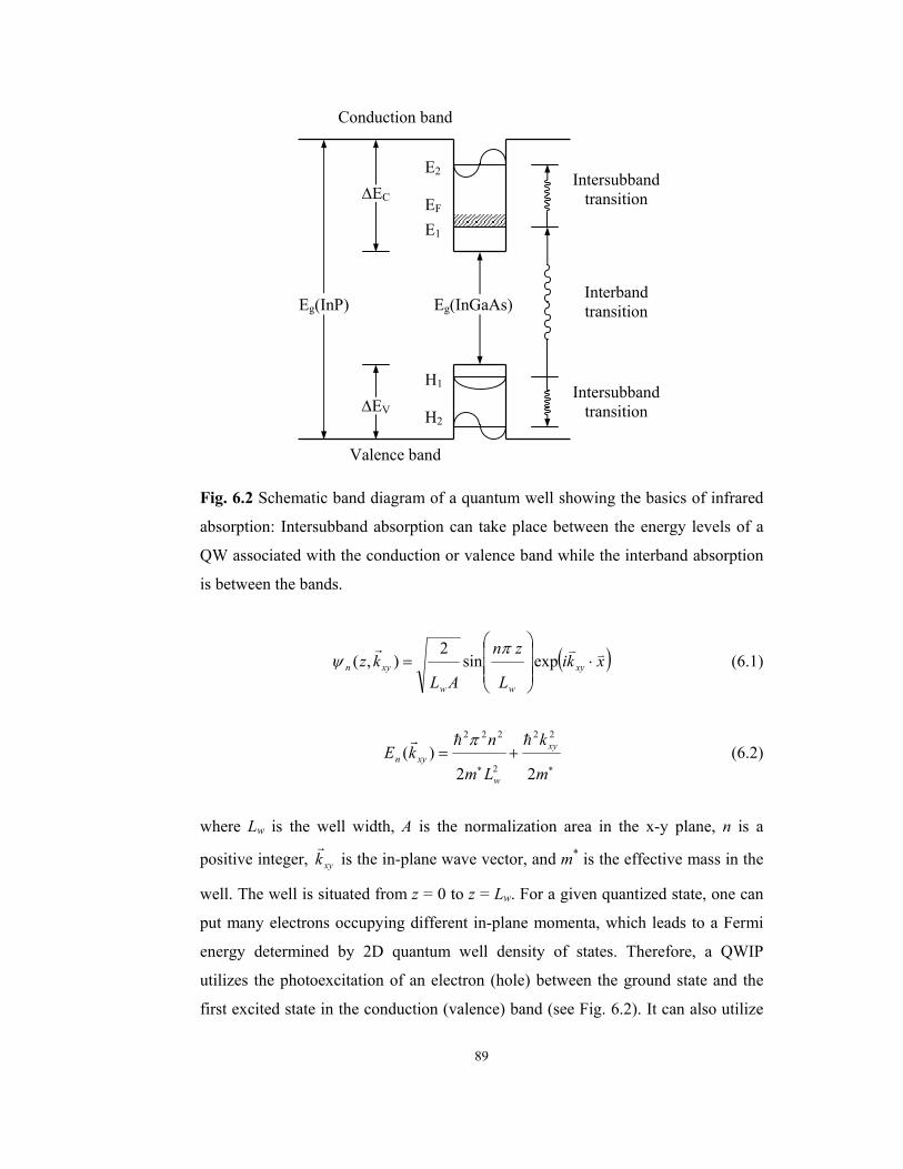
72
100 200 300 400 500 600 700
-15
-10
-5
0
5
10
Vapplied = 20 mVΦeffective = 120 meV
Ln(J
/T2 ) [
ln(A
/cm
2 K2 )]
1/kT (eV-1)
experimental lineer fit
sample 1111
Fig. 4.6 Activation energy plot for determination of barrier height.

73
CHAPTER 5
INTERNAL PHOTOEMISSION SPECTROSCOPY FOR PtSi/p-Si
INFRARED DETECTORS
Internal photoemission spectroscopy (IPS) is an efficient technique in studying the
opto-electronic properties of a metal-semiconductor junction. The barrier height
determined from an IPS measurement is more reliable than other techniques
because it does not usually suffer from non-ideal contributions. On the other hand,
the measurement procedure and the experimental setup are more complicated than
others. Delicate instrumentation and careful light handling are required especially
when the interested spectrum lies in the infrared region.
PtSi/p-Si Schottky diodes serve as infrared detectors in 3-5 µm atmospheric
window. In spite of their low quantum efficiency, PtSi/p-Si junctions have been
successfully used in the infrared imaging systems [96,97]. The process
compatibility with the existing Si technology has made them possible to integrate
PtSi-Si diodes to the existing microelectronic technology. Thus, the electrical [98]
and optical [26,58,99-102] properties of PtSi/p-Si junctions have been subject of
investigation. The modified Fowler theory is commonly used to find the Schottky
barrier height (i.e. the cut-off wavelength of the detector) of these diodes. It is,
however, known that this approach does not agree with the experimental results
especially for photon energies close to the barrier height of the Schottky junction
[61]. The barrier height values extracted by this approach are usually greater than
the actual value [61]. Several studies have been reported on a complete theoretical
formulation of the internal photoemission in metal-semiconductor junctions,

74
particularly in PtSi-Si diodes [59-61,103]. Mooney and Silverman [61] improved
the modified model by taking all possible scattering mechanisms in the thin PtSi
layer into account. However, this theoretical model has not been widely used due to
the simplicity of the common form of the Fowler approach. A comparative study is
then needed to test the validity of the extended model. Additionally, the features of
the internal photoemission spectrum of PtSi-Si diodes in the whole range of the
atmospheric window (3-5 µm) are not well studied. A loss of photoresponse is
usually observed in the high-energy side of the window (~3 µm -0.4 eV-)
[26,101,103,104]. This loss was attributed to parasitic barrier heights present at the
junction [104]. The same behavior was also observed for other detector structures
such as SiGe/Si heterojunctions [30,86], GaAs quantum wells [105] and IrSi3/Si
Schottky diodes [106].
This chapter presents the properties of internal photoemission in PtSi/p-Si.
Theoretical model and the results were discussed in chapter 2 for heterojunctions.
The model is adapted to metal/semiconductor systems and its comparison with the
experimental results is given in this chapter. The effects of various experimental
conditions are also reported. Part of this chapter has been published and can be
found in [76].
5.1 Internal Photoemission in Metal/Semiconductor Systems
In this section, instead of setting up the model for metal(silicide)/semiconductor
internal photoemission infrared detector systems from the beginning, different
points from the HIPs will be introduced to the model presented in chapter 2, since
the operation mechanism in both structures is the same.
Fig. 5.1 shows the detailed energy levels in metal/p-semiconductor band structure.
Since the 0 eV energy reference point is different (bottom of the conduction band of
the metal film), and the energy of the absorbed photon (hν) is less than the Fermi
energy (EF), distribution of excited electrons can be written in momentum space
only as
k(EF - hν) < k < k(EF) (5.1)

75
Fig. 5.1 Energy levels in metal-semiconductor band structure.
From the conservation of total energy, the equivalence of Eq. (2.4) which
determines the escape volume in momentum space is written as
Φ−≤
++⊥
F
smm
Ekmmm
k 2//
222 11
22
hh (5.2)
where mm and ms are the effective masses in the metal film and the Si substrate
respectively. As seen from Eq. (5.2), the equality is satisfied for an ellipsoid of
revolution in k-space no matter what effective masses’ magnitudes are. Thus, the
states which will emit are shown as hatched region in Fig. 5.2. This region is known
as the ‘escape cap’. For the escape cap
)(min νhEkk F −=
)(max Φ−= FEkk (5.3)
The yield can then be written from the volume ratio of the escape cap and the shell
of excitation as
hν hν
EF - Φ
Φ
EF - hν
Metal Semiconductor
Bottom of the conduction band 0
EF

76
( ) ( )[ ] ( )( )
( ) ( )[ ]2/32/3
2/32/32/3
12
11
ν
νν
hEEM
hEMMhMEEM
V
VY
FF
FFF
shell
cF
−−+
−+−Φ++−+Φ−==
(5.4)
In the limit that EF >> hν >> Ψ the yield is approximately
( )
ν
ν
hE
hMY
F
F
8
22/1 Φ−
= (5.5)
Eq. (5.5) is known as the modified Fowler equation and traditionally used in the
analysis of the junction.
Fig. 5.2 Escape cap for holes in momentum space. The hatched region corresponds
to the holes that may escape over the barrier.
This model only differs from the model presented in chapter 2 in the calculation of
the maximum yield while incorporating the scattering mechanisms into it. By using
the fact that EF > Φ and EF > hν, the maximum yield is written as
ν
ν
h
hY
Φ−=∞ (5.6)
As a result, for M = 1, EF >> hν >Φ, and neglecting the quantum mechanical
reflections, the partial yield Yn term in Eq. (2.36) is reduced to
k(EF)
k(EF - hν)
Spherical shell of excitation
Escape cap

77
( )2
8
*)/(*Φ−−= ων
νhnh
hdE
LdULY
F
n (5.7)
where
[ ( ) ] */1*)/( 32*/ LeLdU Ld L+++++= − δδδβα (5.8)
5.2 Experimental Details
PtSi/Si diodes were fabricated on p-type (100) Si substrates with a resistivity of 25-
30 Ωcm. The samples were first cleaned by using a standard RCA cleaning process.
Then they were immediately loaded into a vacuum chamber for the Pt evaporation
process. A 50 Å thick Pt film was deposited on the sample's surface by e-beam
evaporation at a rate of 1.5 Å/sec (UNIVEX 450 system with an e-beam gun
ESV4). In this process a metal shadow mask with circular openings of a diameter of
1 mm was used to define the active regions. The base pressure of the chamber
before the evaporation was 1x10⁻⁶ Torr; it dropped to 1x10⁻⁵ Torr during
evaporation. The PtSi film was formed by annealing the samples at 675 °C for 30
minutes under N2 atmosphere. This high annealing temperature was used to reduce
the oxygen related problems in the PtSi film formation [107]: Under this
temperature the reaction between Pt and Si can be too rapid to trap both unreacted
Pt and Pt2Si in the PtSi lattice. And it is also known that high annealing temperature
does not cause the film of poor quality [108]. The samples were finally fixed on a
sample holder that can be mounted into a closed cycle He cryostat with a special
window which allows infrared light to reach the sample surface. The electrical
contacts to the samples were taken from the implanted guard ring and from the
backside as shown in Fig. 5.3.
Fig. 5.3 Cross-section of the PtSi/p-Si diodes.
Alp-Si
SiOAl
PtSi n+n+

78
The experimental set-up for the internal photoemission measurements is shown in
Fig. 5.4. A globar IR source is used for illuminating the sample. Before entering the
monochromator (ORIEL, MS257) the light is filtered with a long pass filter with a
cut-on wavelength of 2.35 µm. By using a mirror system a small fraction of the
monochromatic light at the exit of the monochromator is directed onto a
pyroelectric reference detector. The undeflected part of the light illuminates the
photodiode mounted on the sample holder in the cryostat (Cryophysics). The signals
from the pyroelectric detector and from the PtSi/p-Si diode are measured by using a
radiometer (ORIEL, Merlin) and an electrometer (Keithley, 6517), respectively.
The measurements are controlled and recorded by a personal computer.
The yield of a photodiode is defined as the ratio of the number of photoelectrons to
that of incident photons. While the number of photoelectrons was determined
directly from the measured photocurrent, that of incident photons was estimated by
measuring the light falling on the sample from a calibrated pyroelectric detector.
The amount of light transmitted through the sample was determined by measuring
the transmission spectrum through the sample. The ratio between the reflected and
absorbed light was estimated from previously reported results [62].
Fig. 5.4 Optoelectronic spectrum measurement system.
Beam splitter
Light source Monochromator Filter
Computer
Cryostat
Sample
Chopper
Pyroelectric detector
Vacuum pump
Electrometer
Radiometer

79
5.3 PtSi/p-Si Spectrum
Fig. 5.5 shows the internal photoemission spectrum of a PtSi/p-Si diode at 70 K.
The dip seen at 0.4 eV (~3 µm) results from the absorption of the incident light by
the thin ice layer formed on the sample during the cooling process and will be
discussed in the following section. When a straight line (dashed line in the graph) is
fitted to the linear portion of the curve, the barrier height is found to be 0.274 eV.
This value of the barrier height is higher than what is usually obtained from I-V
measurements (~0.25eV) [98]. The traditional Fowler theory (Eq. (5.5)) relies on
ballistic transport of photo-excited carriers and ignores their interaction with
phonons, other carriers and film walls. It then overestimates the barrier height of the
junction [61]. As seen in Fig. 5.5 the experimental points do not follow the straight
line of Eq. (5.5) especially for energies close to the barrier height. This commonly
observed feature of the curve is due to the effect of multiple reflections of the
excited holes from the surfaces of the silicide film and that of collisions with
phonons, imperfections and cold electrons. The solid line in the graph represents the
theoretical internal yield of Eq. (2.36) with Eq. (5.7). In the calculations, Eq. (5.8)
was approximated by [1 − exp(− d/L*)]1/2 [59]. Scattering by phonons and electrons
and by the film walls, and the energy lost during electron-phonon collisions are thus
taken into account. In the fitting process, Lp, Le, and ћω were used as adjustable
parameters. For the result showed in Fig. 5.5, Lp=60 Å, Le=2000 Å, ћω=0.006 eV.
These values are within the ranges suggested for holes in PtSi [61]. As shown in
Fig. 5.5, a perfect fit to the experimental data was obtained for the whole spectrum
except for the dip region. The nonlinear part below 0.35 eV is well accounted for by
this model. The barrier height used in this fitting is 0.244 eV which is consistent
with the reported values for PtSi-Si junctions [98]. One can then conclude that the
extended theoretical approach that takes the scattering mechanisms into account
provides a more consistent explanation for the internal photoemission process. We
should, however, note that the result of extended theory is not unique because of too
many adjustable parameters involved in the calculations such as Lp, ћω, and Le.
Unfortunately, reliable values for these parameters are not available, and they are
not easily measurable quantities. Some speculative estimations are available in the
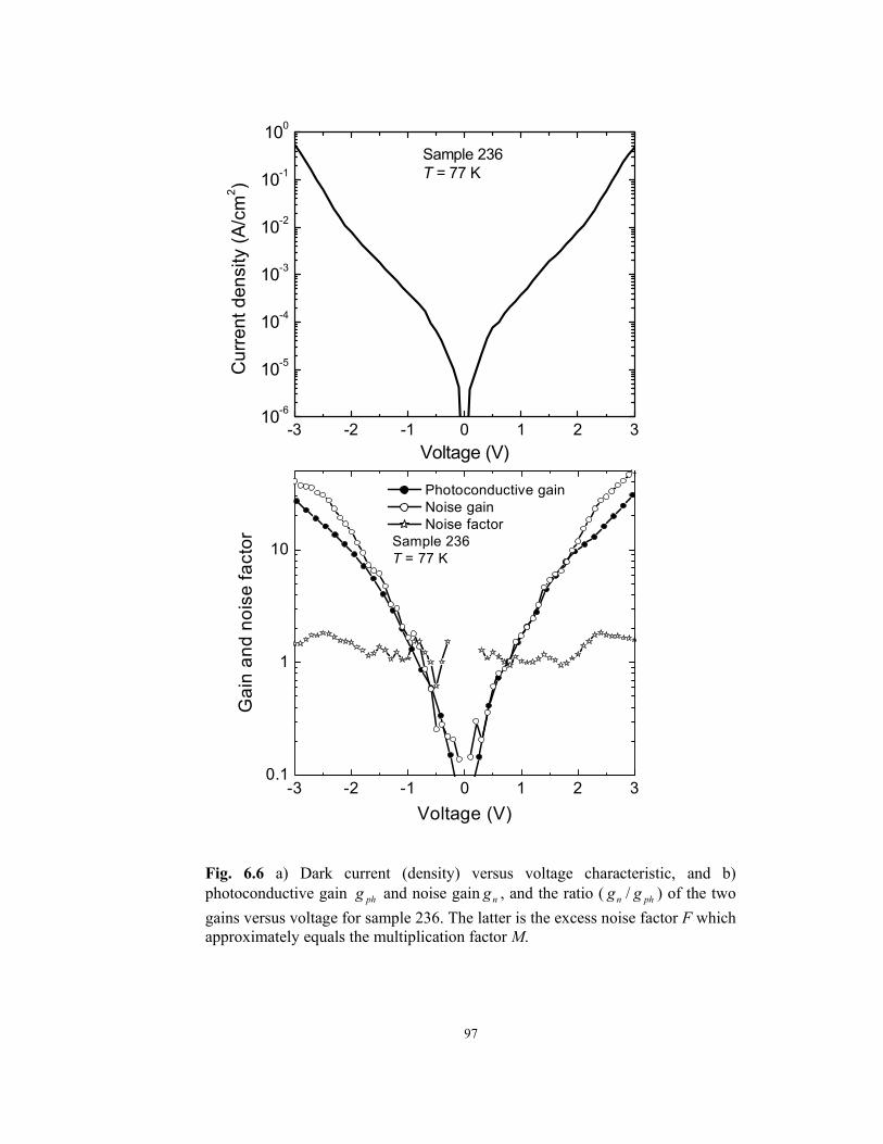
80
literature. We used these estimations in our calculations and obtained consistency in
the results.
0.25 0.30 0.35 0.40 0.450.00
0.01
0.02
0.03
0.04(Y
ext *
hν)
1/2 (e
V)1/
2
Energy (eV)
Extended theory Modified Fowler theory Experimental
Fig. 5.5 Internal photoemission spectrum of the PtSi/p-Si diode. Curves fitted by
modified Fowler theory and extended theory are also shown.
5.4 Effect of the Ice Formation on the Detector’s Response
In the internal photoemission spectrum of a PtSi/p-Si diode shown in Fig. 5.5 a dip
is seen at about 0.4 eV (~3 µm). The position of the dip along the horizontal axis is
same in all measurements but its depth varies under different experimental
conditions. The same dip was also observed in similar experiments by others
[26,30,86,101,103-106]. However, either they ignored the presence of the dip
because this would not affect the results of their work [26,30,86,101,103,106] or
speculated on the reason for the incongruity [104,105]. The same spectral dip at
around 3 µm is seen in many devices having different materials and structures.
Among them there are Schottky devices using Pd2Si [26,104], IrSi3 [106], SiGe/Si
heterojunction infrared detectors [30,86] and GaAs based quantum wells [105]. We
have shown that the foregoing dip in the spectrum is due to the formation of thin ice
layer on surface of the detector during the cooling process.

81
0.25 0.30 0.35 0.40 0.450.00
0.01
0.02
0.03
0.04
(Yex
t * hν
)1/2 (e
V)1/
2
Energy (eV)
Rotary pump Diffusion pump Diffusion pump with heat cycle
( a )
2.0 2.5 3.0 3.5 4.0 4.51
2
3
4
5
6
7
8
9
10
(b)
Norm
alized Absorption
Wavelength (µm)2.0 2.5 3.0 3.5 4.0 4.5
0
5000
10000
15000
20000
25000
30000
A
bsor
ptio
n (1
/cm
)
Fig. 5.6 a) Effect of different vacuum conditions on the internal photoemission
spectrum of the PtSi/p-Si diode. b) Direct comparison of the observed dip to the
spectrum of the ice taken from Ref. [109]. (Experimental data are normalized
against the theoretical response curve). The solid line (ice’s absorption spectrum)
belongs to the left axis and the others (experimental data) belong to the right axis.
Marker types are same as (a).

82
In order to see how this loss in the photoresponse is related to the detector’s
ambient, the experiment was repeated by using different vacuum conditions. For the
case in which a mechanical (rotary) pump was used, the starting pressure during the
cooling down process was about 1x10⁻² Torr. In the other case a diffusion pump
with a liquid N2 trap, which provided a starting pressure of 1x10⁻⁴ Torr, was used to
evacuate the system. The internal photoemission spectra obtained for these
conditions are displayed in Fig. 5.6a. It is seen that the depth of the dip is
considerably reduced when a diffusion pump is employed. In the last experiment,
the sample was first cooled down to 70 K and then heated quickly up to 300 K and
cooled down again without breaking the vacuum created by the diffusion pump. In
this cycling process, the sample is locally heated while the cryostat’s body is still at
very low temperature. The water condensed on the sample’s surface is then
expected to be evaporated from the sample and captured by the cryostat’s cold body
which acts as an effective cryopump. The internal photoemission spectrum of the
diodes obtained after this cycling process is shown in Fig. 5.6a. It is seen from this
spectrum that the dip at 0.4 eV is further reduced with this heat-cool cycle. In
addition, when the position of the dip is compared with the absorption spectrum of
the ice, a correlation between the spectra is clearly seen. Fig. 5.6b shows the
comparison of the ice’s absorption spectrum [109] with the detector’s response
normalized against the theoretical curve fitted nicely to the experimental data (see
Fig. 5.5). It is seen that the spectrum of the ice has a strong absorption peak at 3.078
µm and this coincides exactly with the observed dip in our experiments. This
indicates that the observed loss in the photoresponse resulted from the absorption in
the ice layer formed on the detector’s surface. The incident light is partly absorbed
in this ice layer before reaching the surface of the diode. Taking the peak absorption
coefficient as k=2.5x10⁻⁴ cm-1, the thickness of the ice layer can roughly be
estimated to be 0.1-0.8 µm from the normalized curves shown in Fig. 5.6b. The
amount of the ice would of course depend on the quality of the vacuum and the
relative speed of the cooling process for the parts of the cryostat’s cold stage.
We proved the presence of the same ice effect on the detector’s spectrum for GaAs-
based quantum well systems in another study [110]. It was shown that the

83
speculated double peak behavior was not actually two peaks but one peak and one
dip superimposed on each other. It was again seen that when the detector Dewar
was evacuated more effectively, the dip was almost disappeared.
5.5 I-V Characteristics of PtSi/p-Si Diodes
Even though it has several drawbacks, determination of the Schottky barrier height
from the I-V measurements is a widely used technique in this area. We have mainly
focused on the internal photoemission of the PtSi/Si Schottky junction in this work.
I-V measurements provided supplementary results on the electronic structure of
PtSi/Si interface.
Fig.5.7 shows both forward and reverse bias characteristics of the PtSi-Si diode.
The overall characteristics of the diode are consistent with what is expected for this
diode. Due to the low Schottky barrier height PtSi/Si junction is an ohmic contact
with a low junction resistance at room temperature. In order to see its rectifying
properties and the diode action, it should be cooled down to a certain temperature
below which the carriers do not have enough thermal energy to surmount the barrier
from the metal side to the semiconductor side. This is why the PtSi/Si infrared
detectors should be cooled down to observe their detector action. An exponential
dependence and a rectification were observed below 100 K in the diodes used in
this work. The barrier height and ideality values were determined below this
temperature only.
In the extraction of the barrier height and the ideality factor, the thermionic
emission theory was used and all other current mechanisms were ignored. The
thermionic emission current is given by
Φ−=
nkT
qV
kTTAAIth expexp2*
=
nkT
qVII satth exp (5.9)

84
0.00 0.05 0.10 0.151E-10
1E-9
1E-8
1E-7
1E-6
1E-5
1E-4
1E-3
300 K 150 K 100 K 70 K 50 K
lnI (
A)
Voltage (V)
( a )
0.0 0.2 0.4 0.6 0.8 1.0 1.2 1.41E-10
1E-9
1E-8
1E-7
1E-6
1E-5
1E-4
1E-3
( b )
lnI (
A)
Voltage (V)
300 K 150 K 100 K 70 K 50 K
Fig. 5.7 I-V characteristics of the PtSi/p-Si diode at different temperatures for (a)
forward and (b) reverse bias. Fitted lines for the extraction of the barrier height and
the ideality factor are also shown.

85
where V is the applied voltage, A is the diode area, A* is the effective Richardson
constant and n is called the ideality factor accounting for other current mechanisms.
In the analysis of the reverse I-V characteristics, the equation
=′
kT
cVII satsat
4/1
exp (5.10)
was used and done by plotting lnI vs V1/4 plot as shown in Fig.5.7b. The results are
displayed in Table 5.1. We see that the Schottky barrier height values determined
both from reverse and forward characteristics at 100 K are close to what is expected
for a PtSi/Si junction. Also the ideality factor is close to unity for this temperature.
The barrier height decreases and the ideality factor gets higher values as
temperature decreases. This behavior is typically observed in the non-ideal Schottky
junctions. The reason is that other current mechanisms such as tunneling and
recombination current become more important as the temperature is reduced and the
thermionic current is suppressed. It is then reasonable to assume that the Schottky
barrier height determined at higher temperatures are closer to the true value. This is
consistent what we have obtained in the I-V measurements.
Table 5.1 Barrier height and ideality factor (n) values extracted from I-V analysis
of PtSi/p-Si diodes at various temperatures.
FORWARD REVERSE
Temp (K) 100 70 50 100 70 50
BH (eV) 0.24 0.186 0.132 0.253 0.189 0.130
n 1.285 1.546 1.66 - - -
The barrier height values of PtSi/p-Si obtained by I-V analysis and internal
photoemission spectroscopy (IPS) analysis are displayed in Table 5.2. The
difference between the barrier heights found by using the Modified Fowler theory
and using the extended theory is due to the multiple reflections of the excited holes
from the surfaces of the metal film and the collisions with phonons and
imperfections as discussed before. As a result of these processes, hot holes, which

86
have initially no chance to be captured, are redirected to the interface and pass
through the barrier. Thus, the yield increases. This increase in the yield makes the
aforementioned difference in the analysis.
When one compares the optical and the electrical barrier heights, it is obvious that
there is an excellent agreement between them. And consequently it can be
concluded that the analysis of the internal photoemission spectroscopy by using the
extended model yields the most accurate values for the barrier height.
Table 5.2 Barrier height values of PtSi/p-Si obtained by I-V analysis and internal
photoemission spectroscopy (IPS) analysis.
I-V IPS
Forward Reverse Extended Modified
BH (eV) 0.24 0.253 0.244 0.274

87
CHAPTER 6
InGaAs/InP QUANTUM WELL INFRARED PHOTODETECTORS
Modern growth techniques allow the fabrication of low-dimensional semiconductor
heterostructures of almost any desired design: from two- and one-dimensional
(quantum wells and wires) down to zero-dimensional (quantum dots). These
structures are of high interest due to their technological potential, ranging from
commercially available devices such as solid-state lasers and detectors based on
quantum wells, up to more advanced goals such as using quantum dots to build a
quantum computer.
A common feature of all these systems, which makes them different from the
structures mentioned in the previous chapters, is their quantization of valence and
conduction band into discrete levels. This causes an effective confinement of charge
carriers within the structures. In quantum wells, for instance, carriers can move
freely within a plane, but the motion perpendicular to it (i.e. the growth direction) is
quantized into so-called subbands. Note that, there was no restriction on the carriers
in SiGe/Si and PtSi/Si structures mentioned before; they were free to move in all
directions. As in the extreme case of a quantum dot, all degrees of freedom are
quantized, and the system has an atomic-like density of states. The density of states
(DOS) is an important concept in the device performance since the optical response
is affected fairly by the number of carriers in the structure. Fig. 6.1 shows the
density of states for 0, 2, and 3-dimensional carries.
Leaving the discussion of the 0-dimensional structures’ application as an infrared
photodetector to the next chapter, 2-dimensional case is discussed in this chapter.

88
After giving the basic principles of quantum well infrared photodetectors (QWIP) in
section 6.1, some experimental observations of InGaAs/InP dual-band quantum
well photodetectors and their theoretical discussions are given for the rest of the
chapter. Part of this chapter has been published and can be found in [111].
Fig. 6.1 Density of states versus energy for 0, 2, and 3-dimensional carries.
6.1 Basic Principles of QWIPs
The idea of using multiple quantum well structures to detect infrared radiation can
be explained by using the basic principles of quantum mechanics. The quantum
well is equivalent to the well-known particle in a box problem in quantum
mechanics, which can be solved by the time-independent Schrödinger equation. The
solutions to this problem are the eigenvalues that describe the energy levels inside
the quantum well in which the particle is allowed to exist. The positions of the
energy levels are primarily determined by the quantum well dimensions (height and
width). For infinitely high barriers and parabolic bands, which is the simplest model
to describe the physics, the eigenstate wavefunction and the energy levels are given
by
Free Carrier
3D
Quantum Well
2D
Quantum Dot
0D
DO
S
ENERGY
~ E1/2 constant ~ δE

89
Fig. 6.2 Schematic band diagram of a quantum well showing the basics of infrared
absorption: Intersubband absorption can take place between the energy levels of a
QW associated with the conduction or valence band while the interband absorption
is between the bands.
( )xkiL
zn
ALkz xy
ww
xynvvr⋅
= expsin
2),(
πψ (6.1)
∗∗+=
m
k
Lm
nkE xy
w
xyn
22)(
22
2
222 hhr π (6.2)
where Lw is the well width, A is the normalization area in the x-y plane, n is a
positive integer, xykr
is the in-plane wave vector, and m* is the effective mass in the
well. The well is situated from z = 0 to z = Lw. For a given quantized state, one can
put many electrons occupying different in-plane momenta, which leads to a Fermi
energy determined by 2D quantum well density of states. Therefore, a QWIP
utilizes the photoexcitation of an electron (hole) between the ground state and the
first excited state in the conduction (valence) band (see Fig. 6.2). It can also utilize
E2
E1
H1
H2
Eg(InGaAs) Eg(InP)
Conduction band
Valence band
Intersubband transition
Interband transition
Intersubband transition
EF ∆EC
∆EV

90
the transition between the bands. Depending on the position of the first excited
states, transitions are labeled as bound-to-bound (B-B), bound-to-quasi bound (B-
Q), and bound-to-continuum (B-C) when the excited state is within the well, at the
well and pushed out the well, respectively.
6.2 InGaAs/InP Dual-Band QWIP
Quantum well infrared photodetectors (QWIPs) [43,81] have become a standard
technology for infrared detection and imaging applications over the past decade
[112]. As the band structure of a QWIP can be accurately designed and controlled,
some multicolor and multispectral devices have been implemented [81]. Most of
these devices cover mid-infrared (MIR) and far-infrared (FIR) spectral regions. For
some applications, it is desirable to have a detector working not only in MIR or FIR
but also in the visible and near infrared (NIR) regions. In this regard, InGaAs/InP
[113] and GaAs/AlGaAs [114] based dual-band quantum well photodetectors for
the detection of NIR/MIR and visible/MIR radiation, respectively, have been
reported. The idea of dual-band operation is straightforward: While the
intersubband electron (or hole) transitions are used for MIR detection, visible/NIR
radiation is detected by means of interband transitions. In this chapter, the dual-
band detection with the intersubband part having both bound-to-bound and bound-
to-continuum transitions for the InGaAs/InP materials system are further
demonstrated. Therefore, it has been determined that the parameters for designing
optimal QWIPs for this materials system, completing the original demonstration on
an un-optimized InGaAs/InP structure [113]. In addition, regarding the device
physics of QWIPs, most issues have been adequately resolved [81]. However, we
don’t yet fully understand the responsivity versus voltage characteristics especially
for high-applied fields. The observed responsivity saturates for some samples (for
example in [114]) while increases exponentially-like for other samples (for example
in [113]). Early results were attributed to an avalanche multiplication process due to
intraband impact ionization [43]. As another point of the study, experimental results
of both responsivity and noise measurements and analyze the data using the theory
in [115] are presented.

91
6.3 Experimental Details
Two samples, labeled as 235 and 236, were grown on semi-insulating InP substrates
by chemical beam epitaxy. Both consist of 20 periods of InGaAs wells and InP
barriers with InP top and bottom contacts of 500 and 800 nm, respectively. The
targeted In content is 53%, i.e., the InGaAs is lattice matched to InP. The contacts
were doped with Si to 1.5x1018 cm-3. Sample 235 (236) has 6.6 nm (6.0 nm) n-type
InGaAs wells and 31.2 nm (30.2 nm) undoped InP barriers. The wells were doped
with Si to 3x1011 cm-2 by center δ doping. X-ray and photoluminescence
measurements were done on the two wafers. The layer thicknesses given above
have been slightly refined according to the X-ray result. The PL measurement
indicates that sample 235 probably has a lightly lower In content than that for 236,
by about 2%. A schematic energy band diagram of the device under bias is shown
in Fig. 6.3a. Mesa devices of 400x400 and 600x600 µm2 in sizes were fabricated
with NiGeAu top ring contacts to allow normal incidence illumination for NIR
detection. A 45o edge facet was polished for light coupling to the intersubband
transitions [42] (Fig. 6.3b). For spectral photoresponse measurements a closed cycle
helium cryostat with KBr window and a Bomem DA8 Fourier transform
spectrometer were used. For the MIR region a globar infrared source and a KBr
beamsplitter were used, while for the NIR region a quartz halogen source and a
quartz beamsplitter were used. All photoresponse measurements were performed at
a cryostat temperature of 77 K. The MIR responsivity calibrations were done using
a 1000-K blackbody infrared source, with the excitation wavelength selected by a
variable narrowband filter. A quartz halogen source and a grating monochromator
with a long pass filter were used to make NIR responsivity calibrations. Noise
measurements have been performed using the method of [116].
6.4 Spectral Photoresponse
Fig. 6.4 shows the normalized spectral photoresponse curves for both MIR and NIR
regions. MIR curves correspond to the transition from the confined quantum well
state E1 to confined state E2 for sample 235 (i.e. bound-to-bound:B-B) and to the
continuum states for sample 236 (i.e. bound-to-continuum:B-C). The spectral width

92
Fig. 6.3 a) Schematic energy-band diagram of the device used here under bias. The
arrows indicate the processes for dual-band detection. b) 45o facet measurement
geometry for the light coupling.
of B-C transitions (sample 236) is substantially wider than that of B-B transition
(sample 235) and the peak position is shifted to a higher energy [117,118]. The
MIR response band centered at about 9.4 µm (0.132 eV) and 8.6 µm (0.144 eV) for
samples 235 and 236, respectively. By considering the confined quantum well states
in both conduction and valence bands, labeled as HH1 and HH2 for the heavy hole,
and LH1 and LH2 for the light hole valence band, all features in the NIR part of the
graph can be accounted for [113]. The large turn-on at about 1.01 eV for sample
235 and 1.06 eV for 236 is due to the onset of HH2 to E2 transition. The small step
below 0.9 eV is due to the weak signal of HH1 to E1 and LH1 to E1 transitions. The
sharp cut-off at 1.4 eV is due to the absorption of the incident light in the InP
substrate because of the backside illumination measurement geometry through the
45o facet. Under normal incidence through the top window, for NIR detection,
spectra are broader in the higher energy region (with a drop coming from the InP
top contact at ~1.4 eV) because of the contribution of the photoexcited carriers
within the barrier region. Moreover, one could replace the InP top contact with
InGaAs InP
MIR
NIR
E1
E2
HH1 HH2 LH1 HH3
LH2
IR
45o
z
( a ) ( b )
93
wider band-gap materials such as InAlAs or InAlAsSb, leading to a wider spectral
response in the shorter wavelengths.
We can make a simple effective mass calculation to compare with the spectral
features in Fig. 6.4 [117,119]. The following parameters are used: InGaAs/InP
electron effective mass me = 0.041/0.08, InGaAs/InP heavy hole effective mass mHH
= 0.45/0.6, InGaAs/InP light hole effective mass mLH = 0.052/0.089,
conduction/valence band offset ∆EC/V = 0.21/0.38 eV, and the bandgap of InGaAs
(at 77 K) Eg,InGaAs = 0.82 eV. We concentrate on sample 236 because 235 may be
slightly lattice mismatched. The results of the calculation are indicated in Fig. 6.4
by arrows pointed to the expected transition positions. Note that the effect of the
non-parabolic conduction band is included in the calculation with the non-
parabolicity parameter α = 1.24 eV-1. Note also that E2 is a virtual state in
resonance with the top of the barrier.
0.10 0.15 0.20 1.0 1.2 1.4
0.0
0.2
0.4
0.6
0.8
1.0LH2 −> E2
HH3 −> continuum
HH2 −> E2
LH1 −> E1
HH1 −> E1
Spe
ctra
l pho
tore
spon
se
Photon energy (eV)
sample 235 sample 236
77 K
E1 −> E2
Fig. 6.4 Spectral photoresponse curves for samples 235 and 236 at device
temperature of 77 K. The two parts are separately normalized. The spectral shapes
are insensitive to the bias values and voltages in the range of 2 – 3 V are used for
the curves shown.

94
6.5 Responsivity versus Voltage
The responsivity-voltage characteristics of both devices are shown in Fig. 6.5.
Measurements in MIR were performed at the peak positions of the spectral
photoresponse curves, i.e. at 9.4 µm for sample 235 and at 8.6 µm for sample 236
(see Fig. 6.4). For NIR calibration 0.96 µm (1.3 eV) light was used for both devices.
As shown in Fig. 6.5 both devices display the same trend: a higher responsivity in
MIR than that for NIR and a rapid increase in high voltage region, reaching up to 26
A/W at –3.5 V for sample 235 and 12 A/W at 3.1 V for 236. The obtained
responsivity values are much higher than those for typical GaAs/AlGaAs QWIPs
[118]. Since sample 235 uses bound-to-bound transitions in both spectral regions, a
clear delay in the turn-on of the photoresponse as a function of voltage was
observed [118]. Consistent with this assignment, sample 236 shows nearly no turn-
on delay in responsivity versus voltage plot since the transitions are bound-to-
continuum (Fig. 6.5b). Moreover, comparing Figs. 6.5a and 6.5b it can be seen that
the absolute responsivity values for B-C transitions (sample 236) are higher than
those for B-B transitions (sample 235) up to about ±3V (~23 kV/cm) because of the
relatively high photoexcited escape probability. On the other hand, at higher electric
fields the responsivity for sample 235 exceeds that for sample 236. This may be
caused by the higher peak absorption quantum efficiency in this B-B sample than
that for a B-C situation [117].
6.6 Noise and Avalanche Multiplication
The high responsivity values observed here, similar to the ones in [113] and much
higher than those in standard GaAs/AlGaAs QWIPs [118], are attributed to two
factors. (I) The InP barriers used here have a higher mobility than that for AlGaAs.
(II) There is an avalanche multiplication process due to intraband impact ionization
of electrons out of the quantum wells [43]. To quantitatively identify the
contribution of the avalanche process, we performed noise measurement and carried
out analyses according to the theory described in [115]. The avalanche process is
described by a multiplication factor M, and can be taken into account by replacing

95
0
5
10
15
20
25
Res
pons
ivity
(A/W
)
sample 235 MIR NIR
77 K
( a )
-3 -2 -1 0 1 2 3
0
2
4
6
8
10
12
( b )
Res
pons
ivity
(A/W
)
Voltage (V)
sample 236 MIR NIR
77 K
Fig. 6.5 Responsivity versus voltage characteristics of (a) sample 235 and (b)
sample 236 at device temperature of 77 K. Measurements in MIR were performed
at 9.4 and 8.6 µm for samples 235 and 236, respectively. For NIR calibration 0.96
µm light was used for both devices.

96
the photoconductive gain phg by Mg . Therefore, the detector current responsivity
is written as [115,116]
Mghv
eR η= (6.3)
where g is the “net” gain that the QWIP would have in the absence of the
avalanche process. Similar to [115,116], the generation-recombination noise current
in the presence of avalanche multiplication is written as
MFgBIeI drgn 42, =− (6.4)
where the noise gain ng is replaced by MFg , dI is the dark current, B is the
measurement bandwidth, and F is the excess noise factor. From Eq. (6.3) and Eq.
(6.4), the photoconductive gain gMg ph = and noise gain MFggn = differ by the
noise factor F . Note that the definition of F used here differs from [115] by a
factor of two.
For sample 236 the deduced photoconductive gain phg and the noise gain ng by
means of Eq. (6.3) and Eq. (6.4) are shown in Fig. 6.6, together with the dark
current versus voltage characteristic. For the photoconductive gain calculation
%5=η was used. Up to a voltage ±1.8V (~14kV/cm) where there is no
multiplication process both gain values are the same ggg nph == , and then noise
gain increases more rapidly than photoconductive gain, confirming the existence of
the excess noise factor F. The ratio of the two gains (i.e. F) is also plotted in Fig.
6.6. To relate the noise factor F to the avalanche multiplication M for the present
unipolar photoconductor, we follow the model in [115]:
)2/11( MMpMF +−−= , where p is the capture probability. In the limit
of 1<<p , which is true here, we have MF ≈ . The curve in Fig. 6.6 for F therefore
represents the magnitude of M. It is then implied that for low voltages (|V|<2 V)
there is no multiplication (M=1) and at high voltages (|V|>2 V) the multiplication
factor reaches approximately two ( 2≈M ). It is not understood why M and F

97
-3 -2 -1 0 1 2 310-6
10-5
10-4
10-3
10-2
10-1
100
-3 -2 -1 0 1 2 30.1
1
10
Figure 4 of 4(B. Aslan et al.)
Gai
n an
d no
ise
fact
or
Voltage (V)
Photoconductive gain Noise gain Noise factor
Sample 236 T = 77 K
Sample 236T = 77 K
Cur
rent
den
sity
(A/c
m2 )
Voltage (V)
Fig. 6.6 a) Dark current (density) versus voltage characteristic, and b)photoconductive gain phg and noise gain ng , and the ratio ( phn gg / ) of the two gains versus voltage for sample 236. The latter is the excess noise factor F which approximately equals the multiplication factor M.

98
saturate rather than keep increasing with bias. A larger observed M and F values
would have provided a stronger evidence of avalanche multiplication. It is also
interesting to get a feeling of the magnitude of the impact ionization probability for
an electron traversing one quantum well, labeled as q . Using the expression derived
in [115] )/( qppM −= , for a multiplication of 2=M , we have 2/1/ =pq . We
point out that the observed M of our InP-based devices is in the same range as found
in InGaAs/GaAs QWIPs [116], whereas gph is about one order of magnitude higher.
InGaAs/InP QWIPs thus enable high photoresponse without penalty from excess
noise. The multiplication process also influences the dark current. Fig. 6.6 shows a
more rapid increase in dark current for voltages larger than about |V|>2 V. Note that
for the device sizes used here (400x400 and 600x600 µm2) the dark current does not
exceed 2 mA. In this low current regime, the measurements of responsivity and
noise are reliable and are not affected by series and contact resistances.

99
CHAPTER 7
DETAILED CHARACTERIZATION OF A SYSTEMATIC SET OF
QUANTUM DOT INFRARED PHOTODETECTORS
With the successful usage of quantum well structures for infrared photodetectors,
sensors and imaging systems [43,81], the quantum dot infrared photodetector
(QDIP) has attracted a lot of interest in recent years [48-50,120,121]. Among
QDIPs, the most widely studied ones are made of self-assembled InAs dots on
GaAs substrate.
In general, QDIPs are similar to QWIPs but with the quantum wells replaced by
quantum dots. Different from quantum wells, quantum dots have size confinement
in all spatial directions. Fig. 7.1a shows the schematic layers of a QWIP and a
QDIP. In both cases, the detection mechanism is based on the intraband
photoexcitation of electrons from confined states in the conduction band wells or
dots into the continuum. The potential profile at the conduction band edge along the
growth direction for both structures would have a similar shape as shown in Fig.
7.1b. In fact, it would be exactly the same if the dots were aligned in the growth
direction. In practice, since the dots investigated here are self-assembled and the
barriers are made thick to suppress dark current, they are not correlated between
layers.
An ideal QDIP is expected to be substantially superior to QWIP. Therefore, the area
of QDIP research is very active in the last couple of years. Although there have
been many papers published on self-assembled QDIPs, some critical issues have not
been adequately addressed and clearly resolved. In the following section, the

100
anticipated advantages of QDIPs with simple theoretical basis are enumerated.
Then, some of the issues such as the polarization behavior and the effect of the
number of electrons occupying the dots are discussed by studying a systematic set
of samples with varying the doping density and hence the number of electrons. We
address these issues using the simplest physical picture and neglect higher order
effects such as the effect of wetting layers and the effect of random (modulation)
doping and dot distributions on the photoconductive transport properties. Note that
some of this chapter’s content have been published and can be found in [122,123].
7.1 Anticipated Advantages of QDIPs
“QDIPs allow normal incidence”. A limitation of QWIPs is that, due to the
transition selection rules, they are not sensitive to normally incident light, and they
typically only have a narrow response range in the infrared [43,124]. Note that,
“normally incident light” is the light which is normal to the wafer along the growth
direction. On the other hand, QDIPs do not suffer from this normal-incidence
limitation because of the geometry with the carrier confinement in all three
directions. The normal incidence property is advantageous because it avoids the
need of fabricating a grating coupler in the standard QWIP imaging arrays [112].
Furthermore, QDIPs can have a broader infrared response range because the self-
assembled dots have several discrete states [125,126]. Although normal incidence
response of QDIPs has been reported in the literature [50,127-130], most of the
publications do not show polarization dependence of the photocurrent spectra, and
some [131-133] show dominant P-polarized response in the 45-degree facet
geometry (see Fig. 6.3b). In one publication [134] on absorption measurements
clear evidence of absorption features due to in-plane confined quantum dot levels
was reported. The possible reason of this problem is discussed in section 7.3.
“QDIPs have lower dark current”. Another potential advantage of QDIPs over
QWIPs is the theoretical prediction of lower dark currents in QDIPs [135]. The
simplest way to estimate the dark current is by the following expression [81]
Ddark neJ 3υ= (7.1)

101
Fig. 7.1 Schematic (a) layers of a QWIP and QDIP and (b) potential profile for both
structures under bias.
Top contact
Barrier
Barrier
Bottom contact
Well / Dots
QWIP QDIP
x N x N Growth direction
Emitter
Collector
hν
( a )
( b )

102
where υ is the drift velocity for the electrons in the barrier and n3D is the three-
dimensional electron density in the barrier. Note that the diffusion is neglected in
Eq. (7.1). The electron density can be estimated by [81]
−
=
Tk
ETkmn
B
aBbD exp
22
2/3
23
hπ (7.2)
where mb is the barrier effective mass and Ea is the thermal activation energy which
equals the energy difference between the top of the barrier and the Fermi level in
the well or dot. The difference in the dark current for similar barriers in a QWIP and
a QDIP (i.e. υ and mb are comparable) is then determined by the difference in Ea. If
the field induced barrier lowering effect in Ea is neglected (valid for low applied
fields), the activation energy relates to detection cut-off wavelength (λc) by
F
c
QWIPa E
hcE −=
λ (7.3)
for a QWIP with a bound-to-continuum detection scheme, and for QDIP
c
QDIPa
hcE
λ= (7.4)
where EF is the Fermi level in the well. Thus, it can be seen from the Eq. (7.3) and
Eq. (7.4) that for the same cut-off wavelength and barrier material, there is a
reduction in the dark current in QDIP versus QWIP.
“QDIPs have higher responsivity”. The final advantage relates to the potentially
long excited electron lifetime, τlife. It has been anticipated [136] that the relaxation
of electrons is substantially slowed when the inter-level spacing is larger than
phonon energy – “phonon bottleneck” [137]. If the phonon bottleneck can be
implemented in a QDIP, the higher responsivity values are obtained. Because a
photoconductor responsivity is given by [81]

103
gh
eR η
ν= (7.5)
where η is the absorption efficiency and g is the photoconductive gain [81]
trans
lifegτ
τ= (7.6)
where τtrans is the transit time across the device. Thus, a long τlife directly drives the
large responsivity R.
7.2 Experimental Details
Using molecular beam epitaxy, four samples with nominally identical parameters
except for the modulation delta-doping densities in the GaAs barriers were grown.
Starting with semi-insulating GaAs substrates, the layers are (in growth sequence):
an undoped 300-nm GaAs buffer layer, a 760-nm n+-GaAs bottom contact layer, a
5-nm GaAs spacer layer, QDIP active region, and a 400-nm n+-GaAs top contact
layer. The active region consists of 50 layers of self-assembled InAs QDs separated
by 30-nm GaAs barriers that are center modulation delta-doped with Si to populate
the QDs. The top and bottom contact layers were doped to 1.2×1018 cm-3 with Si to
act as reservoirs of charged carriers (electrons). Mesa devices were made using
standard GaAs microfabrication techniques. The mesas were defined by wet
chemical etching, and the top and bottom contacts were made by depositing
Ni/Ge/Au followed by annealing.
Doping levels per QD layer for samples used in this study are: 1×1010 cm-2 (due to
the background doping) for sample A, 1.5×1010 cm-2 for sample B, 2×1010 cm-2 for
sample C, and 3.5×1010 cm-2 for sample D. By estimating the QD density from
structural observations (from atomic force microscopy and plan-view transmission
electron microscopy) on the three samples grown under the same condition, the
average number of electrons per dot was calculated as 2, 5, 7 and 12 for the four
samples, respectively. Table 7.1 shows the structural parameters used for

104
estimation. For the photoresponse measurements, 400×400-µm2 devices were
mounted in a closed-cycle helium cryostat. A Bomem DA8 Fourier transform
infrared spectrometer with a globar source was used. Devices were illuminated
through the 45o polished edge facets. Data were taken with two sets of beamsplitters
and windows, and corrected by background spectra. To obtain a complete spectrum,
two parts were joined together by superimposing the overlapped region. The
responsivity calibrations were done using a 1000-K blackbody infrared source, with
the excitation wavelength selected by a variable narrowband filter. All
photoresponse measurements were performed at a cryostat temperature of 6 K and
no qualitative differences were seen up to ~30 K, except an increase in the noise
level.
Table 7.1 Structural parameters obtained from atomic force microscopy and plan-
view transmission electron microscopy observations to estimate the number of the
electrons per dot.
Sample QD Density
(1010 cm-2)
Doping per period
(1010 cm-2)
Electrons per dot
(1010 cm-2)
A 0.5 1 2
B 0.3 1.5 5
C 0.3 2 7
D 0.3 3.5 12
7.3 Physical Picture
The electronic shell structure and the level separations of InAs/GaAs self-assembled
QDs are determined by the dot size and shape [138,139]. In general, these self-
assembled QDs are wide in the in-plane direction (~20 nm) and narrow in the
growth direction (~3 nm). Therefore, the strong confinement is in the growth
direction while the in-plane confinement is weak resulting in several levels in the
dots [45]. Samples used in this study have disk-shaped QDs with a diameter of
about 18 nm and a height of about 2.5 nm. Then, in cylindrical coordinates the
Schrödinger equation can be written as

105
),,(),,(),(11
2 2
2
2
2
2
2
zrEzrzrVzrr
rrrm
θθθ
Ψ=Ψ
+
∂
∂+
∂
∂+
∂
∂
∂
∂−h
(7.7)
To clearly illustrate the physical picture and as an approximation, we view the
confining potential in the growth direction (chosen as the z coordinate) and the in-
plane directions (x-y) as being separable. The former is the familiar quantum well
problem. Since the height of the QDs is much smaller than its radii, the electron
motion in the growth direction is strongly confined. Therefore the wavefunction of
an electron may be written as [140]
)()(2
1),,( zrezr n
rnl
il ψψπ
θ θ=Ψ (7.8)
where n represents the distinct subbands related to the vertical motion (n = 0,1,…).
In our case the disks support only one confined level in the growth direction
(ground state, n = 0) [140]. The in-plane circular shape leads to the z-component
angular momentum being a good quantum number (l). Then, for each angular
momentum l and subband index n = 0, )(rlψ satisfy the equation
lrlrl EV
r
l
rr
rrmψψ
ψ=
++
∂
∂
∂
∂−
2
22 1
2
h (7.9)
Analogous to real atoms, the bound states are grouped into three shells: s, p and d.
The d shell has two degenerate angular momentum states, under the parabolic
potential approximation, with quantum numbers l = ±2 and l = 0 [45].
For light polarized in the growth direction, E//z, only transitions (∆l = 0) from
bound to continuum states are allowed. On the other hand, for the in-plane polarized
light, E//x or E//y, the allowed transitions are those changing the angular momentum
by ∆l = ±1, and therefore both bound-to-bound and bound-to-continuum transitions
are possible. To obtain the observed photocurrent, the final state must be either in

106
Fig. 7.2 Schematic conduction band inter-shell transitions in a self-assembled
InAs/GaAs quantum dot. Solid and dotted arrows represent transitions for E//z and
E//x-y polarized lights, respectively. The top part is for transitions originating from
the s shell, and the bottom for p shell.
-2 -1 0 +2 +1Angular Momentum (l)
Ener
gy
s
p
d
E//z strong
E//x strong
E//x weak
( b )
-2 -1 0 +2 +1Angular Momentum (l)
Ener
gy
s
p
d
E//z strong
E//x weak
( a )
E//x strong but no photocurrent

107
the continuum or close to the continuum, i.e., the d shell, so that the photoexcited
electrons can escape. Additional details are given in [141]. Fig. 7.2 shows
schematically some of these possible transitions. The solid arrows indicate
transitions that are sensitive to E//z light whereas dotted ones are for E//x light. The
top panel shows transitions originating from an electron occupying the s shell. For a
given polarization, the transition oscillator strength is strong for going to the nearest
allowed state, for example, for E//x, s to p is strong whereas s to continuum is weak.
Similarly, the bottom panel shows transitions from the p shell.
7.4 Results and Discussion
Dark current characteristics of all samples at two different temperatures, 77 K and 6
K, are shown in Fig. 7.3. A generally expected behavior is seen with varying the
number of electrons. Since the dark current is proportional to exp(-Ea/kBT) [81,121],
where Ea is the activation energy and T is temperature, it decreases with decreasing
number of electrons per dot because activation energy is determined by the electron
number inside the dot [142]. On the other hand, when the temperature of the
samples is reduced, the current due to thermally excited electrons are significantly
suppressed. The irregularities below 200 pA in Fig. 7.3b is due to the electrical limit
of the coaxial cable used in the measurements. Fig. 7.3b also shows clear tunneling
features through the GaAs barrier especially for sample D, which are studied in
more details in [142].
Fig. 7.4 shows the normalized spectral photoresponse curves of samples A, B and C
under P- and S-polarized lights in the mid-infrared. For the highest doping sample
(D), all the energy levels in the dots are filled with electrons (12 e-/dot). The very
small activation energy leads to a high dark current and therefore a high noise
current which prevents the spectral response measurements. The measurement
geometry is shown in the inset. Note that the P-polarized light contains both E//x
(50%) and E//z (50%) components; whereas the S light is only E//x. We have
chosen the x coordinate to coincide with the S-polarization direction. The main
broad peak (Fig. 7.4a) corresponds to the transitions from s and p shells to the
continuum (see also Fig. 7.2), which cover an energy range above ~130 meV. The

108
10-10
10-9
10-8
10-7
10-6
10-5
10-4
10-3
10-2
10-1
-4 -2 0 2 410-10
10-9
10-8
10-7
10-6
10-5
10-4
10-3
10-2
10-1
(a)
D
C
B
AC
urre
nt (A
)
77 K
Cur
rent
(A)
(b)
D
C
B
A
Voltage (V)
6 K
Fig. 7.3 Dark current characteristics for all samples at two different temperatures,
77 K (a) and 6 K (b).
response under S-polarized light (Fig. 7.4b) is weaker than that for P because low
lying bound-to-bound transitions from s to p shell and from p to d shell exhaust
most of the oscillator strengths. In contrast, the largest E//z oscillator strength for
both s and p initial states is the one going into the continuum because there are no
other lower allowed final states. As the number of electrons per QD increases, the
population of the higher states is enhanced. As a result, the transitions to the
continuum states from the higher p shell become more prominent and the

109
photoresponse curve broadens toward the lower energy region. For sample A with
an average of 2 electrons per dot, ideally only the lowest s shell is occupied.
However, due to the random distribution of dopants in relation to dot positions,
some dots have more than 2 electrons leading to a non-zero occupation on the p
shell. For samples B and C, both s and p shells are occupied. For the same reason of
randomness, d shells are occupied in some dots.
0.0
0.2
0.4
0.6
0.8
1.0
100 150 200 250 300 3500.0
0.2
0.4
0.6
0.8
1.0
Nor
mile
zed
phot
ores
pons
e
P-polarizationT=6 K
sample A sample B sample C
P
S
IR
45o
z
(b)
(a)
Sca
led
phot
ores
pons
e
Photon energy (meV)
S-polarizationT=6 K
sample A sample B sample C
Fig. 7.4 Comparison of mid-infrared photoresponse curves of samples having
different numbers of electrons per dot for (a) P-polarized and (b) S-polarized lights.
The P-spectra are normalized to unity, while the S-spectra are scaled by the same
amounts for comparison. The inset to the bottom panel shows the experimental
geometry.

110
Since the peak feature in the range from 70 to 90 meV displays a strong S-polarized
(E//x) response, it is attributed to the transition from a lower confined state to a
higher one, i.e., from p to d shell (see Fig. 7.2b). This feature increases in strength
with the electron number because the p shell is more occupied, and becomes
comparable in height to the broad main feature for sample C shown in Fig. 7.4a.
This is a clear and strong observation for in-plane polarized response in QDIPs.
The spectral response curves in the far-infrared are shown in Fig. 7.5. The behavior
in this region is more complicated and we can offer only a hand-waving
interpretation. For samples B and C, the peaks in the 40-70 meV range are believed
to be caused by the transition from the highest occupied d shell into the continuum.
The reason for peaks appearing at different positions and having different
polarizations is not clear and may be due to electron-electron interactions. Phonons
may also play a role since the energy scales are close to the phonon energies of the
system. The dark region lying in between 32 and 37 meV is a result of longitudinal
optical and transverse optical (TO) phonon absorptions. The dip at ~66 meV comes
from the 2TO absorption [143]. The photoresponse spectrum in this region is thus
further complicated since this entire region lies within the one- and two-phonon
absorption bands. Since sample A has only 2 electrons per dot, the d shell should be
completely empty. It therefore should show no response in this spectral region. This
is true in experiments except just above and below the phonon dark region. The two
peaks at just above and below the dark region may be caused by the phonon
absorption, perhaps coupled with inter-shell transitions. It is known that if a dipole-
transition resonance is close to phonon energy, the electron-phonon interaction
leads to a strong modification of the spectrum and a coupled mode behavior [144].
Clearly the far-infrared characteristics need further study to arrive a fully consistent
interpretation.
Fig. 7.6 shows the responsivity versus voltage characteristics of samples A, B and C
at 7.14 µm (174 meV). All samples display a peak characteristic as a function of
voltage. Starting from zero voltage the increase can be attributed to the increase in
the carrier escape efficiency and in the transport mobility, but the reason for the
decrease at larger voltages is not clear. Note the very high values of responsivity

111
0.0
0.2
0.4
0.6
0.8
1.0
30 40 50 60 70 800.0
0.2
0.4
0.6
0.8
1.0
Nor
miliz
ed p
hoto
resp
onse
P-polarizationT=6 K
sample A sample B sample C
(b)
(a)
Nor
miliz
ed p
hoto
resp
onse
Photon energy (meV)
S-polarizationT=6 K
sample A sample B sample C
Fig. 7.5 Normalized far-infrared photoresponse curves for (a) P-polarized and (b) S-
polarized lights. To compare the relative magnitudes between P and S responses,
the lower panel curves should be multiplied by 0.6, 0.8, and 3.8 for sample A, B,
and C, respectively, for example, the solid curve in (b) should be multiplied by 0.6
to compare with the curve in (a).
indicating a large photoconductive gain: By using Eq. (7.5) and Eq. (7.6), the
photoconductive gain can be estimated speculatively as ~70 for R = 4 A/W, hν =
0.174 eV and η = 0.01 (since the absorption in these samples is low). For drift
velocity υ = 2×107 cm/s (the maximum velocity for the electrons in the GaAs [92]),
and having the device length x = 1600 nm, the transit time (τtrans= x/υ ) and

112
therefore the life time (τlife) can be found as >0.5 ns. This is a couple of order higher
than that for normal QWIP [145]. This value is even larger for R > 4 A/W (sample
C for instance). For samples A and B, there is a delay in the turn-on of the
photoresponse as a function of voltage, and the reason again is not clear. The large
asymmetry in the responsivity curve of sample C is correlated with the low
temperature dark current results (see Fig. 7.3b).
-4 -3 -2 -1 0 1 2 3 40
4
8
12
16
20
24
Res
pons
ivity
(A/W
)
Voltage (V)
sample A sample B sample C
λ=7.14 µm (174 meV)T=6 KUnpolarized
Fig. 7.6 Responsivity versus voltage characteristics for samples A, B and C at 7.14
µm (174 meV) and 6 K.

113
CHAPTER 8
CONCLUSION
The primary aim of this work was to study the internal photoemission (IP)
mechanism of semiconductor heterojunctions used as infrared detectors in the
mid/far-infrared region. In order to provide a better understanding of the
experimental results, the old and recent theoretical descriptions and models were
reviewed, revised and extended. The extensions incorporate the effects of the
difference in the effective masses in the active region and the substrate,
nonspherical-nonparabolic bands, and the energy loss per collisions on the internal
quantum efficiency of the detector. The model is then completed by incorporating
the wavelength and doping concentration dependent free carrier absorption to the
model. Experiments done in this study have shown that the IP spectrum of SiGe/Si
(in the form of Fowler plot) can be consistently described by this completed
theoretical model. The secondary aim was to study on the infrared photodetectors
having different detection mechanisms and different material systems to complete
the picture of the infrared detector subject. Since the thesis is organized in a way
that each chapter is self-contained/consistent, it would be appropriate to make
conclusion for each chapter separately.
In chapter 3, the mechanisms of photocurrent generation in the SiGe/Si
heterojunction internal photoemission (HIP) infrared photodetectors have been
studied and a qualitative model has been presented. It has been shown that the
performance of our devices depend significantly on the applied bias and the
operating temperature. We obtained 31 µm and 18.2 µm cut-off wavelengths for -37

114
mV and 75 mV, respectively. These cut-off values were extracted by using the
complete model derived in chapter 2 for semiconductor heterojunction systems. It
has been shown that the experimental and theoretical curves are in a very good
agreement. However, the result of the theory is not unique because of the many
adjustable parameters involved in the calculations such as Le, Lp, and ћω.
Unfortunately, reliable values for these parameters are not available and they are
not easily measurable quantities. The tunability feature seen in our devices can be
utilized to design new devices whose cut-off wavelength can be set by the
externally applied voltage. However, device parameters should be optimized for an
efficient application.
The effects of double barrier on the photoresponse spectrum of the SiGe/Si
heterojunction internal photoemission (HIP) infrared photodetectors have been
studied in chapter 4. When compared with the single barrier sample that has
nominally the same parameters, it has been shown that the double barrier sample
acts as a temperature tunable infrared photodetector. From the Fowler analysis we
obtained 22.5 µm and 12.6 µm cut-off wavelength values for 10 K and 50 K,
respectively. Even though the model described in chapter 2 might have not been
applicable to analyze this double-barrier sample, the cut-off values were extracted
by using this model on the basis of the expectation that it must be more reliable than
the other models.
In chapter 5, an example for metal(silicide)/semiconductor systems has been
investigated. We have shown that a theoretical model that includes the effects of
scattering in the PtSi film can consistently describe the internal photoemission
spectrum of a PtSi-Si diode. It has been also shown that the unexpected dip in the
spectrum around 0.4 eV is due to the absorption of light by the ice layer formed on
the sample’s surface during cooling. The formation of ice layer can be reduced by
using more effective pumping systems. The effect of the ice formation on the
detector should be taken into account when designing a detector operating in the
mid-infrared region.

115
The dual-band detection with the intersubband part having both bound-to-bound
and bound-to-continuum transitions for InGaAs/InP quantum wells which are 2-
dimensional systems have been demonstrated in chapter 6. These devices have
shown high responsivity, gain and avalanche multiplication at high bias. The high
responsivity demonstrated in QWIPs with InGaAs/InP materials may be useful for
imaging applications where a short integration time is required.
Finally in chapter 7, an example of 0-dimensional systems has been studied. The
detailed optical characterizations on InAs/GaAs self-assembled quantum dot
infrared photodetectors with various doping levels have been made. The spectral
photoresponse curves in a wide spectral region from the mid- to far-infrared have
been reported. Polarization behaviors of transitions and effects of the number of
electrons on the photoresponse spectra have been demonstrated. A strong in-plane
polarized bound-to-bound transition feature has been observed. A simple picture
has been presented to account for the observed features.

116
REFERENCES
[1] J. M. Lloyd, Thermal Imaging Systems, Plenum Press, New York, 1975
[2] H. A. Gebbie, W. R. Harding, C. Hilsum, A. W. Pryce, and V. Roberts, Proc.
of the Royal Society London A206, 87 (1951)
[3] R. D. Hudson, and J. W. Hudson (eds.), Infrared Detectors, Benchmark
Papers in Optics 2, Halsted Press, Pennsylvania, 1975
[4] R. J. Keyes (ed), Optical and Infrared Detectors, Topics in Applied Physics
19, Springer-Verlag, 1977
[5] E. L. Dereniak and G. D. Boreman, Infrared Detectors and Systems, John
Wiley & Sons, 1996
[6] J. Piotrowski, and A. Rogalski, Sensors and Actuators A 67, 146 (1998)
[7] M. H. Francombe and J. L. Vossen (eds), Advences in Research and
Development, Thin Films 23, Academic Press, 1998
[8] A. Rogalski, Inf. Phys. & Tech. 41, 213 (2000)
[9] A.G.U. Perera and H.C. Liu (eds), Semiconductor Optical and Electro-
Optical Devices, Handbook of Thin Film Devices 2, Academic Press, 2000
[10] A. Rogalski, Progress in Quantum Electronics 27, 59 (2003)
[11] A. Rogalski, J. Appl. Phys. 93, 4355 (2003)
[12] H. C. Liu and F. Capasso (eds), Intersubband Transitions in Quantum wells:
Physics and Device Applications I, Semiconductor and Semimetals 62,
Academic Press, 2000
[13] A. Rose, Concepts in Photoconductivity and Allied Problems, Interscience,
New York, 1963

117
[14] I. Bhat (ed), J. Electron. Mater. 25 (no 8), 1133-1415 (1996)
[15] W. D. Lawson, S. Nielsen, E. H. Putley, And A. S. Young, J. Phys. Chem.
Solids 9, 325 (1959)
[16] J. L. Schmit and E. L. Stelzer, J. Appl. Phys. 40, 4865 (1969)
[17] G. L. Hansen, J. L. Schmit, and T. N. Casselman, J. Appl. Phys. 53, 7099
(1982)
[18] M. Kimata and N. Tubouchi in: A. Rogalski (ed), Infrared Photon Detectors,
SPIE Opt. Eng. Press, 1995, pp. 299-349 (Chapter 9)
[19] F. D. Shephard in: M. H. Francombe and J. L. Vossen (eds), Research and
Development, Thin Films 23, Academic Press, 1998, pp. 83-114
[20] E. H. Rhoderick and R. H. Williams, Metal-Semiconductor Contacts,
Clarendon Press, Oxford, 1988
[21] J. H. Werner and U. Rau, Springer Series in Electronics and Photonics, 32,
89, 1994
[22] W. Schottky, Naturwiss. 26, 843, 1938
[23] N. F. Mott, Proc. Chambr. Phil. Soc. 34, 568, 1938
[24] J. Bardeen, Phys. Rev. 71, 717, 1947
[25] V. Heine, Phys. Rev. A138, 1689, 1965
[26] H. Elabd and W. F. Kosonocky, RCA Review 43, 569, 1982
[27] P. W. Pellegrini, A. Golubovic, C. E. Ludington, and M. M. Weeks, IEDM
Tech. Dig., p157-160 (1982)
[28] B. Y. Tsaur, M. M. Weeks, R. Trubiano, P. W. Pellegrini, T. R. Yew, IEEE
Elect. Dev. Lett. 9, 650 (1988)
[29] F. D. Shephard, V. E. Vickers, and A. C. Yang, U.S. Patent 3,603,847 (1971)
[30] T. L. Lin and J. Maserjian, Appl. Phys. Lett. 57, 1422 (1990)
[31] M. D. Petroff and M. G. Stapelbroek, U.S. Patent 4,568,960 filed in 1980,
granted in 1986

118
[32] S. B. Stetson, D. B. Reynolds, M. G. Stapelbroek and R. L. Stemer, Proc.
SPIE 686, 48 (1986)
[33] F. Szmulowicz and F. L. Madarsz, J. Appl. Phys. 62, 2533 (1987)
[34] S. Tohyama, N. Teranishi, K. Konuma, M. Nishimura, K. Arai, and E. Oda,
IEEE Trans. Electron Dev. 38, 1136 (1991)
[35] S. Tohyama, A. Tanabe, and N. Teranishi, IEEE Trans. on Elec. Dev., 41,
1535 (1994)
[36] A. G. U. Perera, H. X. Yuan and M. H. Francombe, J. Appl. Phys. 77, 915
(1995)
[37] A. G. U. Perera in: A.G.U. Perera and H.C. Liu (eds), Semiconductor Optical
and Electro-Optical Devices, Handbook of Thin Film Devices 2, Academic
Press, 2000, pp. 135-170 (Chapter 5)
[38] T. Ando, A. B. Fowler, and F. Stern, Rev. Mod. Phys. 54, 437 (1982)
[39] L. Esaki and H. Sakaki, IBM Tech. Discl. Bull. 20, 2456 (1977)
[40] J. S. Smith, L. C. Chiu, S. Margalit, A. Yariv, and A. Y. Cho, J. Vac. Sci.
Technol. B 1, 376 (1983)
[41] L. C. West and S. J. Eglash, Appl. Phys. Lett. 46, 1156 (1985)
[42] B. F. Levine, K. K. Choi, C. G. Bethea, J. Walker, and R. J. Malik, Appl.
Phys. Lett. 50, 1092 (1987)
[43] B. F. Levine, J. Appl. Phys. 74, R1 (1993)
[44] J. L. Pan and C. G. Fonstad, Mat. Sci. and Eng. 28, 65 (2000)
[45] L. Jacak, P. Hawrylak and A. Wojs, Quantum Dots, Springer-Verlag, 1998
[46] S. Fafard, Z. R. Wasilewski, C. N. Allen, D. Picard, P. G. Piva, and J. P.
McCaffrey, Superlattices and Microstructures 25, 87 (1999)
[47] S. Fafard, H.C. Liu, Z. R. Wasilewski, J. P. McCaffrey,M. Spanner, S.
Raymond, C. N. Allen, K. Hinzer, J.Lapointe, C. Struby, M. Gao, P.
Hawrylak, C. Gould, A. Sachrajda, and P. Zawadzki, Proc. SPIE 4078, 100
(2000)

119
[48] H. C. Liu, M. Gao, J. McCaffrey, Z. R. Wasilewski and S. Fafard, Appl. Phys.
Lett. 78, 79 (2001)
[49] J. Phillips, K. Kamath and P. Bhattacharya, Appl. Phys. Lett. 72, 2020 (1998)
[50] D. Pan, E. Towe and S. Kennerly, Appl. Phys. Lett. 73, 1937 (1998)
[51] C. Miesner, O. Röthig, K. Brunner, and G. Abstreiter, Physica E 7, 146
(2000)
[52] C. Miesner, K. Brunner, and G. Abstreiter, Inf. Phys. & Techn. 42, 461 (2001)
[53] S. Tong, J. L. Liu, J. Wan and L. L. Wang, Appl. Phys. Lett. 80, 1189 (2002)
[54] C. Kittel, Introduction to Solid State Physics, Wiley, 1986
[55] R. W. Boyd, Radiometry and the Detection of Optical Radiation, Wiley, 1983
[56] N. B. Stevens in: R. K. Willardson and A. C. Beer (eds), Infrared Detectors,
Semiconductors and Semimetals 5, Academic Press, 1970
[57] R. H. Fowler, Phys. Rev. 38, 45 (1931)
[58] J. Cohen, J. Vilms, R. J. Archer, Final Rep. AFCRL-68-0651, Hewlett-
Packard Labs, Palo Alto, CA (1968)
[59] V. E. Vickers, Appl. Optics 10, 2190 (1971)
[60] V. L. Dalal, J. Appl. Phys. 42, 2274 (1971)
[61] J. M. Mooney, J. Silverman, IEEE Trans. Electron Devices ED-32, 33 (1985)
[62] J. M. Mooney, Ph D. Thesis, University of Arizona, 1986
[63] B-Y. Tsaur, C. K. Chen, and S. A. Marino, SPIE 1540, 580 (1991)
[64] H. C. Liu, L. Li, J.-M. Baribeau, M. Buchanan, and J. G. Simmons, J. Appl.
Phys. 71, 2039 (1992)
[65] R. Strong, D. W. Greve, P. Pellegrini, and M. Weeks, J. Appl. Phys. 82, 5199
(1997)
[66] J. S. Park, T. L. Lin, E. W. Jones, H. M. Del Castillo, and S. D. Gunapala,
Appl. Phys. Lett. 64, 2370 (1994)

120
[67] T. L. Lin, J. S. Park, S. D. Gunapala, E. W. Jones, and H. M. Del Castillo,
IEEE Elect. Dev. Lett. 15, 103 (1994)
[68] R. Strong, R. Misra, D. W. Greve, and P. C. Zalm, J. Appl. Phys. 82, 5191
(1997)
[69] Y. Fu, S. C. Jain, M. Willander, and J. J. Loferski, J. Appl. Phys. 74, 402
(1993)
[70] B. Aslan, M. S. Thesis, Middle East Technical University, 1999
[71] H. Hara and Y. Nishi, J. Phys. Soc. Japan 21, 1222 (1966)
[72] H. Presting, J. Konle, M. Hepp, H. Kibbel, K. Thonke, R. Sauer, E. Corbin,
and M. Jaros, Opt. Eng. 39, 2624 (2000)
[73] J. I. Pankove, Optical Processes in Semiconductors, Prentice-Hall, 1971
[74] R. Wang, P. Chen, P. Tsien, G. Luo, J. Zhou, and A. Liu, Inf. Phys. & Tech.
39, 293 (1998)
[75] H. Wada, M. Nagashima, K. Hayashi, J. Nakanishi, M. Kimata, N. Kumada,
and S. Ito, SPIE 3698, 72 (1999)
[76] B. Aslan, and R. Turan, Inf. Phys. & Tech. 43, 85 (2002)
[77] G. Masini, L. Colace, F. Galluzzi, G. Assanto, T. P. Pearsall, and H. Presting,
Appl. Phys. Lett. 70, 3194 (1997)
[78] J. R. Jimenez, X. Xiao, J. C. Sturm, and P. W. Pellegrini, Appl. Phys. Lett. 67,
506 (1995)
[79] C. Schwartz and H. von Känel, J. Appl. Phys. 79, 8798 (1996)
[80] L. Pahun, Y. Campidelli, F. A. d’Avitaya, and P. A. Badoz, Appl. Phys. Lett.
60, 1166 (1992)
[81] H. C. Liu in: H. C. Liu and F. Capasso (eds), Intersubband Transition in
Quantum Wells: Physics and Device Applications I, Academic, San Diego,
2000 Chapter 3
[82] B. Aslan, R. Turan, H.C. Liu, M. Buchanan, and J.-M. Baribeau, Semicond.
Sci. Technol. 19, 399 (2004)

121
[83] H. Lafontaine, D. C. Houghton, D. Elliot, N. L. Rowell, J.-M. Baribeau, S.
Laframboise, G. I Sproule, and S. J. Rolfe, Vac. Sci. Technol. B14, 1675
(1996)
[84] T. L. Lin, A. Ksendzov, S. M. Dejewski, E. W. Jones, R. W. Fathauer, T. N.
Krabach, and J. Maserjian, IEEE Trans. Elect. Dev. 38, 1141 (1991)
[85] H.C. Liu, M. Buchanan, and J.-M. Baribeau, Appl. Phys. Lett. 62, 988 (1993)
[86] R. Banisch, B. Tillack, K. Pressel, R. Barth, and H. Erzgräber, Thin Solid
Films 294, 254 (1997)
[87] C. Renard, S. Bodnar, P. A. Badoz, and I. Sagnes, J. Cryst. Growth 157, 195
(1995)
[88] D. B. Raynolds, D. H. Seib, S. B. Stetson, T. Herter, N. Rowlands, and J.
Schoenwald, IEEE Trans. Nuc. Sci. 36, 857 (1989)
[89] J. E. Huffman, A. G. Crouse, B. L. Halleck, T. V. Downes, and T. L. Herter,
J. Appl. Phys. 72, 273 (1992)
[90] V. V. Rylkov, J. Leotin, L. Asadauskas, B. A. Aronzon, and D. Yu. Kovalev,
J. Appl. Phys. 91, 4511 (2002)
[91] H. C. Liu, J. Li, M. Buchanan, J.-M. Baribeau, and J. G. Simmons, Elect. Lett.
29, 407 (1993)
[92] S. M. Sze, Physics of Semiconductor Devices, John Wiley & Sons, 2nd ed.,
1981
[93] Ö. S. Anilturk, R. Turan, Solid-State Elect. 44, 41 (2000)
[94] A. Köck, E. Gornik, G, Abstreiter, G. Böhm, M. Walther, and G. Weimann,
Appl. Phys. Lett. 60, 2011 (1992)
[95] B. Aslan, R. Turan, H.C. Liu, M. Buchanan, J.-M. Baribeau, and P. Chow-
Chong, Appl. Phys. B. 78, 225 (2004)
[96] W. F. Kosonocky, F. V. Shallcross, T. S. Villani, IEEE Transactions on
Electron Devices ED-32, 1564 (1985)
[97] K. Konuma, S. T. Tohyama, A. Tanabe, N. Teranishi, K. Masubuchi, T. Saito,
and T. Muramatsu, IEEE Transactions on Electron Devices 39, 1633 (1992)

122
[98] V. W. L. Chin, M. A. Green, and J. W. V. Storey, Solid-State Electronics 36,
1107 (1993)
[99] V. W. L. Chin, J.W.V. Storey, and M. A. Green, Solid-State Electronics 39,
277 (1996)
[100] J. M. Mooney, J. Appl. Phys. 65, 2869 (1989)
[101] K. Komuma, Y. Asano, and K. Hirose, Phys.Rev. B 51, 13187 (1995)
[102] A. Czernik, H. Palm, W. Cabanski, M. Schulz, and U. Suckow, Appl. Phys. A
55, 180 (1992)
[103] D. E. Mercer and C. R. Helms, J. Appl. Phys. 65, 5035 (1989)
[104] X. Xiao, J. C. Sturm, S. R. Parihar, S. A. Lyon, D. Meyerhofer, S. Palfrey,
and F. V. Shallcross, IEEE Electron Device Letters 14, 199 (1993)
[105] H. C. Liu, M. Buchanan and Z. R. Wasilewski, J. Appl. Phys. 83, 6178 (1998)
[106] T. L. Lin and J. M. Iannelli, Appl. Phys. Lett. 56, 2013 (1990)
[107] F. Nava, S. Valeri, G. Majni, A. Cembali, G. Pignatel, and G. Queirolo, J.
Appl. Phys. 52, 6641 (1981)
[108] Murarka et al., J. Appl. Phys. 54, 6943 (1983)
[109] G. Warren, Appl. Opt. 23, 1206 (1984)
[110] B. Aslan, H. C. Liu, M. Buchanan and Z. R. Wasilewski, J. Appl. Phys. 91,
10230 (2002)
[111] B. Aslan, H.C. Liu, A. Bezinger, P. J. Poole, M. Buchanan, R. Rehm, and H.
Schneider, Semicond. Sci. Technol. 19, 442 (2004)
[112] S. D. Gunapala and S. V. Bandara in: H. C. Liu and F. Capasso (eds),
Intersubband Transition in Quantum Wells: Physics and Device Applications
I, Academic, San Diego, 2000 Chapter 4
[113] H. C. Liu, C. Y. Song, E. Dupont, P. J. Poole. P. H. Wilson, B. J. Robinson
and D. A. Thompson, Electron. Lett. 35, 2055 (1999)
[114] H. C. Liu, C. Y. Song, A. Shen, M. Gao, Z. R. Wasilewski and M. Buchanan,
Appl. Phys. Lett. 77, 2437 (2000)

123
[115] H. Schneider, Appl. Phys. Lett. 82, 4376 (2003)
[116] R. Rehm, H. Schneider, M. Walther, P. Koidl and G. Weimann, Appl. Phys.
Lett. 82, 2907 (2003)
[117] H. C. Liu, J. Appl. Phys. 73, 3062 (1993)
[118] B. Xing, H. C. Liu, P. H. Wilson, M. Buchanan, Z. R. Wasilewski and J. G.
Simmons, J. Appl. Phys. 76, 1889 (1994)
[119] S. Datta, Quantum Phenomena, Addison-Wesley, 1989
[120] L. Chu, A. Zrenner, G. Bohm, and G. Abstreiter, Appl. Phys. Lett. 76, 1944
(2000)
[121] H. C. Liu, S. Fafard, R. Dudek and Z. R. Wasilewski, Photonics West, paper
4646-11 (2002)
[122] B. Aslan, H. C. Liu, M. Korkusinski, S.-J. Cheng, and P. Hawrylak, Appl.
Phys. Lett. 82, 630 (2003)
[123] H. C. Liu, B. Aslan, M. Korkusinski, S.-J. Cheng, and P. Hawrylak, Inf. Phys.
& Tech. 44, 503 (2003)
[124] H. C. Liu, M. Buchanan, and Z. R. Wasilewski, Appl. Phys. Lett. 72, 1682
(1998)
[125] S. Fafard, R. Leon, D. Leonard, J. L. Merz, and P. M. Petroff, Phys. Rev. B
52, 5752 (1995)
[126] M. Bayer, O. Stern, P. Hawrylak, S. Fafard, and A. Forchel, Nature (London)
405, 923 (2000)
[127] K. W. Berryman, S. A. Lyon, and M. Segev, Appl. Phys. Lett. 70, 1861 (1997)
[128] L. Chu, A. Zrenner, G. Bohm, and G. Abstreiter, Appl. Phys. Lett. 75, 2599
(1999)
[129] A. D. Stiff, S. Krishna, P. Bhattacharya, and S. Kennerly, Appl. Phys. Lett. 79,
421 (2001)
[130] S. Raghavan, P. Potella, S. Stintz, B. Fuchs, S. Krishna, C. Morath, D. A.
Cardimona, and S. W. Kennerly, Appl. Phys. Lett. 81, 1369 (2002)

124
[131] S. J. Xu, S. J. Chua, T. Mei, X. C. Wang, X. H. Zhang, G. Karunasiri, W. J.
Fan, C. H. Wang, J. Jiang, S. Wang, and X. G. Xie, Appl. Phys. Lett. 73, 3153
(1998)
[132] N. Horiguchi, T. Futatsugi, Y. Nakata, N. Yokoyama, T. Mankad, and P. M.
Petroff, Jpn. J. Appl. Phys. 38, 2559 (1999)
[133] S. Sauvage, P. Boucaud, T. Brunhes, V. Immer, E. Finkman, and J.-M.
Gérard, Appl. Phys. Lett. 78, 2327 (2001)
[134] A. Weber, O. Gauthier-Lafaye, F. H. Julien, J. Brault, M. Gendry, Y. Désieres
and T. Benyattou, Appl. Phys. Lett. 74, 413 (1999)
[135] V. Ryzhii, Semicond. Sci. Technol. 11, 759 (1996)
[136] U. Bockelmann and G. Bastard, Phys. Rev. B 42, 8947 (1990)
[137] J. Urayama, T. B. Norris, J. Singh, and P. Bhattacharya, Phys. Rev. Lett. 86,
4930 (2001)
[138] S. Fafard, Z. R. Wasilewski, C. N. Allen, D. Picard, M. Spanner, J. P.
McCaffrey and P. G. Piva, Phys. Rev. B 59, 15368 (1999)
[139] P. Hawrylak, S. Fafard and Z. R. Wasilewski, Condensed Matter News 7
(issue 4), 16 (1999)
[140] M. Korkusinski and P. Hawrylak, Phys. Rev. B 63, 195311 (2001)
[141] P. Hawrylak, M. Korkusinski, S. Fafard, R. Dudek and H. C. Liu, Physica E
13, 246 (2002)
[142] J.-Y. Duboz, H. C. Liu, Z. R. Wasilewski, M. Byloos and R. Dudek, J. Appl.
Phys. 93, 1320 (2003)
[143] M. J. Howes and D. V. Morgan (eds), Gallium Arsenide: Material, Devices
and Circuits, Wiley, Chichester, 1985
[144] H. C. Liu, C. Y. Song, Z. R. Wasilewski, A. J. SpringThorpe, J. C. Cao, C.
Dharma-wardana, G. C. Aers, D. J. Lockwood and J. A. Gupta, Phys. Rev.
Lett. 90, 077402 (2003)
[145] H. C. Liu, Appl. Phys. Lett. 60, 1507 (1992)

125
VITA
Bülent Aslan was born in Ankara on July 16, 1974. He received his B.S. and M.S.
degrees in Physics from the Middle East Technical University (METU) in 1996 and
1999, respectively. Title of his master thesis is “Internal Photoemission
Spectroscopy for PtSi/Si and Pt/SiGe Schottky Type Infrared Detectors”. He has
been working as a research/teaching assistant in the Department of Physics, METU.
Between February 2002 and February 2003, he worked as a Visiting Researcher in
Quantum Devices Group, Institute for Microstructural Sciences, NRC, Ottawa,
Canada.
List of Publications of Bülent Aslan:
1. “Double-barrier long wavelength SiGe/Si heterojunction internal photoemission
infrared photodetectors” B. Aslan, R. Turan, H.C. Liu, J.-M. Baribeau, M.
Buchanan and P.C. Chong, Applied Physics B 78, 225 (2004).
2. “High responsivity, dual-band response and intraband avalanche multiplication
in InGaAs/InP quantum well photodetectors” B. Aslan, H.C. Liu, A. Bezinger,
P. J. Poole, M. Buchanan, Semiconductor Science and Technology 19, 442
(2004).
3. “Mechanisms of photocurrent generation in SiGe/Si HIP infrared
photodetectors” B. Aslan, R. Turan, H.C. Liu, and J.-M. Baribeau,
Semiconductor Science and Technology 19, 399 (2004).
4. “Detailed characterization of a systematic set of quantum dot infrared
photodetectors” H.C.Liu, B.Aslan, M.Korkusinski, S.-J.Cheng, P.Hawrylak,
Infrared Physics & Technology 44, 503 (2003).

126
5. “Response spectra from mid- to far-infrared, polarization behaviors, and effects
of electron numbers in quantum-dot photodetectors” B. Aslan, H. C. Liu, M.
Korkusinski, S.-J. Cheng, and P. Hawrylak, Applied Physics Letters 82 630
(2003).
6. “Erratum: “Short wavelength (1–4 µm) infrared detectors using intersubband
transitions in GaAs-based quantum wells” [J. Appl. Phys. 83, 6178 (1998)]” B.
Aslan, H. C. Liu, M. Buchanan, and Z. R. Wasilewski, Journal of Applied
Physics 91, 10230 (2002).
7. “On the internal photoemission spectrum of PtSi/p-Si infrared detectors”, B.
Aslan and R. Turan, Infrared Physics & Technology 43, 85 (2002).
8. “Observation of strain relaxation in Si1-xGex layers by optical and electrical
characterization of Schottky junction”, R. Turan, B. Aslan, O. Nur, M.Y.A.
Yousif and M. Willander, Applied Physics A 72, 587 (2001).
9. “Internal photoemission spectroscopy for a PtSi/p-Si Schottky junction”, B.
Aslan and R. Turan, Turkish Journal of Physics 24, 577 (2000).
10. “Effect of layer relaxation on the internal photoemission in Pt/Si1-xGex Schottky
barrier type infrared detectors”, B. Aslan, R. Turan, O. Nur, M. Karlsteen and
M. Willander, Material Research Society Symposium Proceedings 607, 235
(2000).
11. “Internal photoemission spectroscopy for a PtSi/p-Si Schottky junction”, B.
Aslan and R. Turan, Proceeding of International School of Solid State Physics
330 (2000), World Scientific.
12. “Correlation between barrier height and band offsets in metal/Si1-xGex/Si
heterostructures”, O. Nur, M. Karlsteen, M. Willander, R. Turan, B. Aslan,
M.O. Tanner and K.L. Wang, Applied Physics Letters 73 (26), 3920 (1998).
International conferences/meetings attended:
1. Materials Research Society (MRS) 1999 Fall Meeting, Boston - USA,
November 29 – December 2, 1999
(Poster presentation: Effect of Layer Relaxation on the Internal Photoemission
in Pt/Si1-xGex Schottky Barrier Type Infrared Detectors)

127
2. International School of Solid State Physics, 16th Course: Silicides:
Fundamentals and Applications, Erice - Italy, June 5-16, 1999
(Poster presentation: Internal Photoemission Spectroscopy for a PtSi/p-Si
Schottky Junction)
National conferences/meetings attended:
1. 5th National Optic, Electro-optic, and Photonic Meeting, Ankara - Turkey,
December 12, 2003
(Oral presentation: InAs/GaAs Quantum Dot and SiGe/Si Heterojunction
Infrared Detectors.)
2. 3rd National Electro-optic Meeting, Ankara - Turkey, November 2, 2001
(Oral presentation: Pt Based Schottky Type Infrared Detectors.)