Embed Size (px)
Citation preview

Electronics for Scientists
Physics 375
Department of PhysicsIllinois State UniversityNormal, IL 61790-4560
Spring 2010B. K. Clark©

Physics 375 Electronics for ScientistsExperiment 1 – Basic Meters and Resistors
In this laboratory exercise you will learn to use power supplies, voltmeters, ammeters, and ohmmeters. These meters usually come in the same package.
Laboratory Exercise:
1. Connect your function generator to your oscilloscope (Fig. 1). Verify that the voltages and time bases of both instruments are in agreement, by comparing the predicted and measured periods and amplitudes approximately three times per frequency decade (10, 30, 70, 100 Hz, etc.). Voltmeters can be used to measure voltages in alternating current, but since it only reports a root mean square (rms), it must average. The voltmeter can be connected across the terminals of the function generator, allowing it to be checked at the same time as the function generator and oscilloscope. What is the highest and lowest frequency at which the voltmeter yields a reliable value. Support your answer with a graph. Why should you use logarithmic scaling for frequency on your graphs?
Figure 1. Figure 2.
2. First measure the resistance of a single resistor with the ohmmeter. Next measure two resistors in parallel and in series. Do the values agree with what you expected? Set up the circuit shown in Fig. 2 using a variable DC power supply, a 22 W resistor, a voltmeter and an ammeter to determine the actual resistance of a resistor that is nominally 22 Ω at 1/8 Watt. Measure the voltage across and current through the resistor at periodic values of applied voltage. Use the 10 Amp input on the ammeter, so that you do not harm the meter. You should obtain approximately ten to fifteen data points when you reach the applied voltage corresponding to 1/8 Watt. Allow approximately 15 to 30 seconds between measurements. Continue making measurements until the current dramatically decreases or the resistor undergoes a significant change to its operational condition. You may need to change the current scale during the experiment. This may introduce a slight error, but it should not be significant. Is there a region where the curve is nonlinear. Remember that resistance is R = dV/dI not R = V/I.
2

Physics 375 Electronics for ScientistsExperiment 2 – Mesh Equations and Thevenin Equivalent Circuits
In this laboratory exercise you will learn compare theoretical calculation to experimental observations. You will also determine the Thevenin equivalent circuit for two voltage sources.
1. Construct the circuit shown in Fig. 1, and measure the voltage across and current through each resistor. Do your results agree with Kirchoff’s voltage and current laws? Now replace the 100 Ω resistor with a potentiometer. What value must the potentiometer have to yield no current flow through the vertical 330 Ω resistor? Do your calculations agree with experiment?
Figure 1.
2. In this part of the laboratory exercise, we will measure the output voltage and current of two voltage sources as a function of the load resistance. Begin by constructing the circuit shown in Fig. 2. Use the function generator with the DC offset set to 10 V and the AC component minimized. Then measure the voltage across and current through the load resistor as its resistance is varied from its maximum value to a very small value. The actual resistance can be determined from the voltage and current measurements. Now, assume the power supply can be modeled as a constant voltage source, VT in series with a resistor RT. What are the values for VT and RT? What if the voltage source is modeled as a constant current source IN in parallel with a resistor RN? Try the same procedure for an 18 V brick or the 12 V output on the regulated supply.
3

Figure 2.
Physics 375 Electronics for ScientistsExperiment 3 – Soldering
In this laboratory you will get an opportunity to practice your soldering techniques by practicing on whatever components the instructor supplies.
4

Physics 375 Electronics for ScientistsExperiment 4 – RC Circuits and Filters
RC circuits can be used in the laboratory as high pass and low pass filters. High frequency voltage fluctuations are measured across the resistor in a series RC circuit used as a high pass filter. The same circuit is a low pass filter when it is used to measure low frequency voltage fluctuations across the capacitor.
Laboratory Exercise:
1. Low Pass Filter: Measure the ratio and relative phase of the peak output voltage across the capacitor, relative to the peak input voltage, for the circuit in Fig. 1 (use a 0.047 µF capacitor and a 475 Ω resistor). At what frequency does the peak voltage across the capacitor drop to ½ the applied voltage? Make the same determination with a 2.2 µF capacitor. Examine as much of the frequency space from 10 Hz to 1 M Hz as possible. Remember the frequency displayed on the function generator is in cyc/sec while the theoretical equations use ω and are in rad/sec.
2. High Pass Filter: Measure the ratio and relative phase of the peak output voltage across the resistor, relative to the peak input voltage, for the circuit in Fig. 2 (use a 0.047 µF capacitor and a 475 Ω resistor). At what frequency does the peak voltage across the resistor drop to ½ the applied voltage? Make the same determination with a 2.2 µF capacitor. As you did in the computer assignment examine as much of the frequency space from 10 Hz to 1 M Hz as possible.
For each set of measurements requiring detailed observations through a range of frequencies, provide a plot of Vout/Vin vs. ω and phase, φ vs. ω. The plots should compare experimental results as individual data points with the theoretically expected values.
Figure 1. Figure 2.
5

Physics 375 Electronics for ScientistsExperiment 5 - Introduction to Logic Gates
In this laboratory exercise you will begin to study the circuit behavior of diodes and basic logic gates. In class we saw that diode circuits may be used to create logical gates. In reality, most digital circuits are based on transistors, but the basic principles can still be understood in terms of diodes.
Laboratory Exercise:
1. Use diodes, a power supply, and a voltmeter to verify the diode representation of an AND gate as in Fig. 1. Build this circuit on your breadboard. Verify that the voltage drop across each diode is approximately 0.7 V. Next, verify the results of the AND operations. Turn in a logic table with actual voltages substituted for high and low logic levels. Do your results agree with a conventional logic table. What happens as the 5 volt bias applied to the pull up resistor is decreased, while one of the inputs is held at 5 volts and the other is grounded?
Figure 1. Figure 2.
2. Transistor-Transistor Logic or TTL refers to a commonly used class of integrated circuits that can withstand serious abuse. Unfortunately it is rather slow and consumes a great deal of power compared to almost any other family of integrated circuits. While slow, it is still ideal for learning about digital electronics and constructing simple control and monitoring circuits for the laboratory. You have a 7408 Quad two-input AND-gate and a 7402 Quad two-input NOR-gate in your parts box. Verify that the output of each of these gates agrees with the corresponding mathematical logic functions. You should probably look up the pinout of each chip before trying to use them. Construct the circuits as in Fig. 2. Be careful, the 7408 and 7402 have different input and output pins. You should turn in a logic table that displays your observations. Report actual observed voltages, not just high or low.
3. Use the NOR gate to determine the minimum high input voltage and maximum low input voltage for the TTL circuit to function properly. One of the inputs to the NOR gate
6

should be tied to ground and the other input to a 0 to 5 V variable power supply. Do not forget that the whole chip needs to be powered at 5 V.
7

Physics 375 Electronics for ScientistsExperiment 6 - Debounced Circuits and Counters
You have looked at the behavior of flip-flops and counters with Electronics Workbench. Now it is time to look at real circuits. You will begin this lab by building a debounced switch. The output of this switch may be used to generate clock pulses for a counter, which is your next task. The binary output of the counter can be displayed on and LED bargraph or decoded through a decoder for further use.
Laboratory Exercise:
1. The debounced switch that you constructed in the last lab will be used to generate clean clock pulses at the Q output. Use this feature to verify the predicted behavior of the J-K master/slave flip-flop contained on a 7476 integrated circuit, shown in Fig. 1. Table 1 shows the logic truth table for the J-K master/slave flip-flop (x – don’t care, N – negative going edge). You only need to do this for the last two sets of conditions. A counter can be constructed based on those conditions. Fig. 1 shows the circuit for observing the last set of conditions.
Table 1
P C Clock J K Q Q’
0 1 x x x 1 01 0 x x x 0 10 0 x x x indeterminate1 1 N 0 0 Qo Qo’
1 1 N 1 0 1 01 1 N 0 1 0 11 1 N 1 1 toggle
Figure 1.
8
Q

2. Counters are one of the simplest and most useful circuits in digital electronics. A 0 to 5 counter can be made by combining a set of J-K master/slave flip-flops, as shown in Fig. 2. Construct this circuit. The outputs labeled C, B, and A make up 3 bit binary numbers, where C is the most significant bit (22) and A is the least significant bit (20). Use the debounced switch to generate the clock pulses.
a) Observe the binary output via the LED bar while inputting clock pulses with your debounced circuit. The outputs of the counter are connected to the high voltage side of the bar (the side with the angled corner), and the low voltage sides of the diodes are connected to ground via 330 Ω resistors.
b) Replace the debounced switch with a signal generator output. Use the TTL output of the signal generator, which provides a nice 0 to 5 volt square wave at the desired frequency. Observe the output of the counter with the frequency set to about 1 Hz. Adjust the frequency as desired.
Figure 2.
3. Modify the counter to a 0 to 15 counter and save it for the next lab.
9

Physics 375 Electronics for ScientistsExperiment 7 – Timers, Clocks, and Decoders
In the lecture part of the course, we learned that the 555 timer can be used to generate clock pulses at regular, user determined intervals. When a timer is connected to a counter and a display, one has a clock. In the last lab, you used an LED bar to display the output states of the counters that you constructed. Now you will replace the LED bar with a decoder and seven-segment display to observe your counter with a hexadecimal display, then you will add a 555 timer circuit so that your system will become a clock.
1. Begin by confirming that your 0 to 15 counter is still operating correctly. Now add a decoder circuit by connecting the output of the counter to the A, B, C, and D inputs of a 7447 decoder chip. The LED bar should still be included in the circuit. Then connect the outputs of the decoder to the corresponding inputs of the seven-segment display via a 330 Ω resistor between each set of connections. As before, Vcc corresponds to a 5 V bias. The seven-segment display has no ground because the outputs of the 7447 go to 0 V when activated. Carefully record the character forms representing each clock pulse.
Table 1. Table 2.
Figure 1.
7447 pinout1-B 16-Vcc2-A 15-f3 14-g4 13-a5 12-b6-D 11-c7-A 10-d8-gnd 9-e
seven-segment display1-a 14-Vcc2-f 13-b3-Vcc 124 11-g5 10-c6 9-dp7-e 8-d
10
a
d
b
c
f g
e
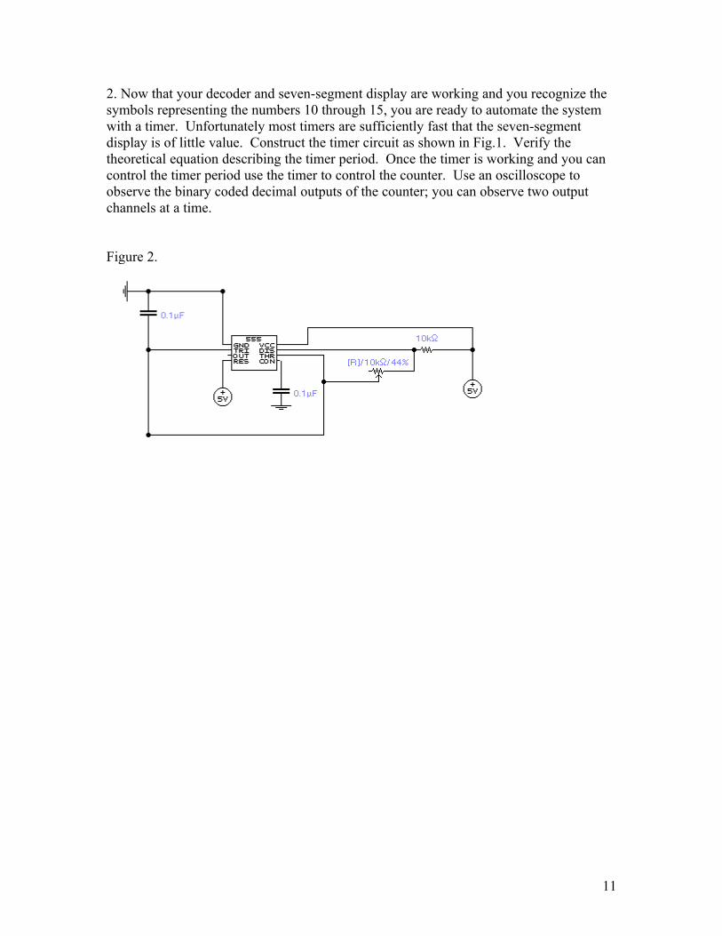
2. Now that your decoder and seven-segment display are working and you recognize the symbols representing the numbers 10 through 15, you are ready to automate the system with a timer. Unfortunately most timers are sufficiently fast that the seven-segment display is of little value. Construct the timer circuit as shown in Fig.1. Verify the theoretical equation describing the timer period. Once the timer is working and you can control the timer period use the timer to control the counter. Use an oscilloscope to observe the binary coded decimal outputs of the counter; you can observe two output channels at a time.
Figure 2.
11

Physics 375 Electronics for ScientistsExperiment 8 - Diodes and Transistors
We have used diodes throughout this course. Now we should look at the actual behavior of diodes and transistors. We will begin by determining the merit of the equation that describes the current-voltage relationship for a diode. Next we will make a simple transistor based amplifier and determine its gain.
Laboratory Exercise:
1. First, set up the circuit shown in Fig. 1. Use the 0 to 12 V supply. Begin at 0 volts, and increase the voltage until the current no longer increases. Record the current as a function of voltage across the diode, with the diode in ice water and then in air. The current equation for a diode,
I = Is (eVq/kT – 1), (1)
does not allow for saturation of a diode. Is is the reverse saturation current, q is the absolute value of the electron charge, k is the Boltzmann constant, V is the voltage across the diode, and T is the temperature of the diode junction. In reality we know that we cannot move an infinite amount of current through the diode. Verify that your data is described by Eq. (1). This is an application where a logarithm might be useful. The resistor serves to limit current, so it should not have to be very large.
Figure 1.
2. Use the same circuit as in Part 1 to measure the forward bias current versus voltage curves for the emitter-base and collector-base junctions of the pnp transistor in air. The pin configuration of the transistor is shown in Fig. 2. Be sure to correctly identify the emitter, base, and collector?
12

3. Set up the transistor amplifier circuit shown in Fig. 3. What is the minimum voltage necessary for the collector to yield a current? What is the gain of the circuit? How does the circuit respond to different waveforms and frequencies? What happens if the resistor at the emitter is removed? Does this agree with what we expect from theoretical considerations? The combination of the AC and DC power supplies are available to you as a function generator.
Figure 2.
Transistor as seen from flat side.
ebc
Figure 3.
13

Physics 375 Electronics for ScientistsExperiment 9 - Operational Amplifiers
You have learned how to build amplifiers with transistors. In reality, transistors are primarily used as individual components when low power integrated circuit technology needs to be interfaced to a load that requires a large power input. Normally, amplifiers are based on operational amplifier integrated circuits. In this laboratory exercise, you will determine the behavior (gain) for a range of frequencies and waveform types for three operational amplifier circuits.
Laboratory Exercise:
1. Begin by building the inverting amplifier shown in Fig. 1. Use Rf = 1 kΩ and then 10 kΩ. Make a plot of output potential vs. frequency for both values of Rf for a sine wave. Record any additional relevant observations (output waveform, for example). Repeat for a square wave. I recommend about three measurements per frequency decade. Consider representing the frequency axis in log format. Do not forget that power must also be supplied to the operational amplifier chip. In this case, you will use all three terminals of your power supply. You will also have to use your data sheet for the 741 operational amplifier to determine the pinout.
Figure 1.
2. Now build the integrating amplifier shown in Fig. 2. Repeat the measurements in Part 1 using only a square wave. Does gain make sense? The typical slew rate for a 741 is 0.5 V/us. Can you interpret the output in terms of this slew rate?
14

Figure 2.
3. Finally, build the differentiating amplifier shown in Fig. 3. Repeat the measurements in Part 1 and the analysis of Part 2. You must determine the most suitable input waveform.
Figure 3.
15

Homework Problems – Introduction and RN
Introduction:
1. How many electrons flow through a cross-section of a wire carrying a current of 1.00 ampere in one second?
2. Mathematically show that the current through the resistor in QUCS-ch1ohmslaw varies like 1/R for a constant voltage.
3. Create the simulation of 2) using QUCS.
4. Prove that the earth has no net charge
RN:
1. Simplify the resistor network in QUCS-ch2aresistornetwork if the negative battery terminal is connected to the junctions of a) R3 and R4, and b) R6 and R5. Repeat for R4 = 100 .
2. Use QUCS to solve 1) for each of the cases.
3. Manually determine the current through and voltage across R5 and R6 in both of the QUCS-ch2resistors simulation if R5 = 100 .
4. Now let QUCS solve the problem using the parameter sweep for R5 varying from 10 to 1 M.
16

Homework Problems - Mesh Equations
17

Homework Problems – Thevenin Equivalent Circuits
18

Homework Problems – Norton Equivalent Circuits
19

Homework Problems – Introduction to Logic Gates
L1. Prove that A xor B = (A + B) * (A * B), where the underline is used to denote the not operation. Draw the circuit diagram that represents this equation.
L2. Prove the associative laws,
A * (B + C) = (A * B) + (A * C)and
A + (B * C) = (A + B) * (A + C),
are valid using truth tables.
L3. Determine the truth table for the following circuit.
L4. Determine the truth table for the following circuit.
20

Homework Problems – Karnaugh Maps
K1. Some seven segment decoders decode the numbers 10 = A, 11= b, 12 = C, 13 = d, 14 = E, and 15 = F. Using a Karnaugh map, determine the logic equation that will function as the decoder for element e as shown in Fig. 1. The logic function must work for all numbers from 0 to 15. Begin by specifying which numbers require the used of element e. Assume your final answer must be represented by a four-input or gate, inverters, and two-input and gates (once you have an equation, represent it by the appropriate combinations of gates). D, C, B, and A should be your labels from most significant bit to least significant bit, respectively.
Figure 1.
K2. Design a comparator that compares one three-bit binary number to a second three-bit binary number. Use a Karnaugh map to determine the logic needed to display a positive output when the first number is less than or equal to the second number. As above, represent the final equation by the appropriate combination of gates.
Homework Problems – Timers
DT1. Choose a set of resistors and a capacitor that will produce a 6.0 ms output pulse on a 10.0 ms repeat cycle using a 555 timer.
DT2. Use the pinout for the 74121 to design a circuit that will generate a 50 ns pulse.
DT3. Add a second 74121 to your solution of DT2 that will produce a circuit that will produce a 50 ns pulse once every 200 ns.
21
a
d
b
c
f g
e

Homework Problems – Operational Amplifiers
OA1. Design an operational amplifier circuit whose output represents (a) 6x –5y and (b) 7x + 3y – 10z.
OA2. Design an operational amplifier circuit whose output represents (a) 10x –7 dy/dt and (b) 5 dx/dt + 3y – 8 ∫ zdt.
OA3. Determine the equation represented by the circuit
OA4. Design a circuit that represents the velocity and position of a ball if the input is the acceleration.
22