Embed Size (px)
Citation preview

Physics 123/223: Final Exam Fall 2013 1
Physics 123/223: Final Exam: Laboratory Electronics. Fall 2013
YOUR NAME: ___________________________
This is a mostly-closed-book test. You may use the following materials:
1. a one-page, one-sided handwritten ’cheat sheet’
2. a schematic diagram of the ’big board’ lab computer;
3. the thick xeroxed handout labeled “. . .References for Microcontroller,” detailing the 8051 instructionset;
4. a calculator (not a web-linked cellphone)
Also, please notice that these exam papers include some information that may be useful:
• An appendix at the end of the papers show some odds and ends:
– Some sketchy device data sheets:∗ 3 op amps: ’411, ’358 & LMC6482 (rail-to-rail)
∗ 3 Comparators
∗ LM317/337 adjustable voltage regulator
∗ power MOSFET
∗ 555 oscillator
∗ 1N5294 current-limiting diode
∗ analog switch (DG403)
– a two-sheet reminder of some details of 8051 assembly language
Please remember to show your work, so that we can give partial credit for imperfect answers.
Total time : 180 minutes. Total points: 158 (analog: 61; digital: 97)
With regret, we must remind you that you need to dismantle your computer. Unless you still areworking on a project, we’d like you to do it right after the exam : melancholy experience has shownus that people rarely return to take apart a computer, despite their good intentions. It’ll take youonly about 10 minutes.
Physics 123/223: Final Exam Fall 2013 2
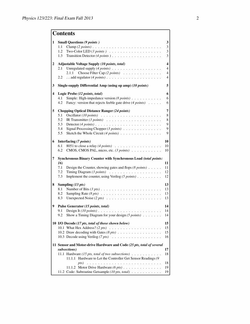
Contents1 Small Questions (9 points ) 3
1.1 Clamp (2 points) . . . . . . . . . . . . . . . . . . . . . . . . . 31.2 Two-Color LED (3 points ) . . . . . . . . . . . . . . . . . . . 31.3 Transition Detector (4 points ) . . . . . . . . . . . . . . . . . . 3
2 Adjustable Voltage Supply (10 points, total) 42.1 Unregulated supply (4 points) . . . . . . . . . . . . . . . . . . 4
2.1.1 Choose Filter Cap (2 points) . . . . . . . . . . . . . . 42.2 . . . add regulator (4 points) . . . . . . . . . . . . . . . . . . . . 4
3 Single-supply Differential Amp (using op amp) (10 points) 5
4 Logic Probe (12 points, total) 64.1 Simple: High-impedance version (8 points) . . . . . . . . . . . 64.2 Fancy: version that rejects feeble gate drive (4 points) . . . . . 6
5 Chopping Optical Distance Ranger (24 points) 75.1 Oscillator (10 points) . . . . . . . . . . . . . . . . . . . . . . 85.2 IR Transmitter (3 points) . . . . . . . . . . . . . . . . . . . . 85.3 Detector (4 points) . . . . . . . . . . . . . . . . . . . . . . . . 95.4 Signal Processing Chopper (3 points) . . . . . . . . . . . . . . 95.5 Sketch the Whole Circuit (4 points) . . . . . . . . . . . . . . . 9
6 Interfacing (7 points) 106.1 8051 to close a relay (4 points) . . . . . . . . . . . . . . . . . 106.2 CMOS, CMOS PAL, micro, etc. (3 points) . . . . . . . . . . . 10
7 Synchronous Binary Counter with Synchronous Load (total points:16) 117.1 Design the Counter, showing gates and flops (8 points) . . . . . 117.2 Timing Diagram (3 points) . . . . . . . . . . . . . . . . . . . 127.3 Implement the counter, using Verilog (5 points) . . . . . . . . . 12
8 Sampling (13 pts) 138.1 Number of Bits (3 pts) . . . . . . . . . . . . . . . . . . . . . . 138.2 Sampling Rate (8 pts) . . . . . . . . . . . . . . . . . . . . . . 138.3 Unexpected Noise (2 pts) . . . . . . . . . . . . . . . . . . . . 13
9 Pulse Generator (15 points, total) 149.1 Design It (10 points) . . . . . . . . . . . . . . . . . . . . . . . 149.2 Show a Timing Diagram for your design (5 points) . . . . . . . 14
10 I/O Decode (17 pts, total of those shown below) 1510.1 What Hex Address? (2 pts) . . . . . . . . . . . . . . . . . . . 1510.2 Draw decoding with Gates (8 pts) . . . . . . . . . . . . . . . . 1510.3 Decode using Verilog (7 pts) . . . . . . . . . . . . . . . . . . 16
11 Sensor and Motor-drive Hardware and Code (25 pts, total of severalsubsections) 1711.1 Hardware (15 pts, total of two subsections) . . . . . . . . . . . 18
11.1.1 Hardware to Let the Controller Get Sensor Readings (9pts) . . . . . . . . . . . . . . . . . . . . . . . . . . . 18
11.1.2 Motor Drive Hardware (6 pts) . . . . . . . . . . . . . . 1911.2 Code: Subroutine Getsample (10 pts, total) . . . . . . . . . . . 19
Physics 123/223: Final Exam Fall 2013 3
ANALOG
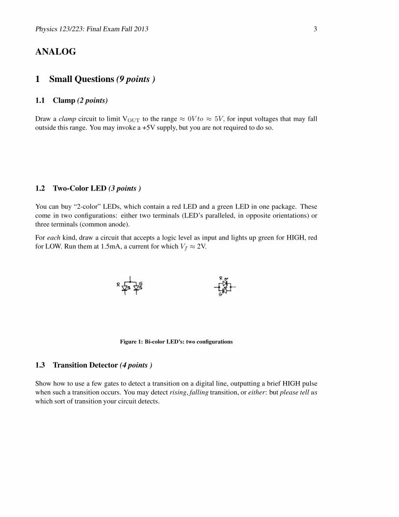
1 Small Questions (9 points )
1.1 Clamp (2 points)
Draw a clamp circuit to limit VOUT to the range ≈ 0V to ≈ 5V, for input voltages that may falloutside this range. You may invoke a +5V supply, but you are not required to do so.
1.2 Two-Color LED (3 points )
You can buy “2-color” LEDs, which contain a red LED and a green LED in one package. Thesecome in two configurations: either two terminals (LED’s paralleled, in opposite orientations) orthree terminals (common anode).
For each kind, draw a circuit that accepts a logic level as input and lights up green for HIGH, redfor LOW. Run them at 1.5mA, a current for which Vf ≈ 2V.
Figure 1: Bi-color LED’s: two configurations
1.3 Transition Detector (4 points )
Show how to use a few gates to detect a transition on a digital line, outputting a brief HIGH pulsewhen such a transition occurs. You may detect rising, falling transition, or either: but please tell uswhich sort of transition your circuit detects.
Physics 123/223: Final Exam Fall 2013 4
2 Adjustable Voltage Supply (10 points, total)
2.1 Unregulated supply (4 points)
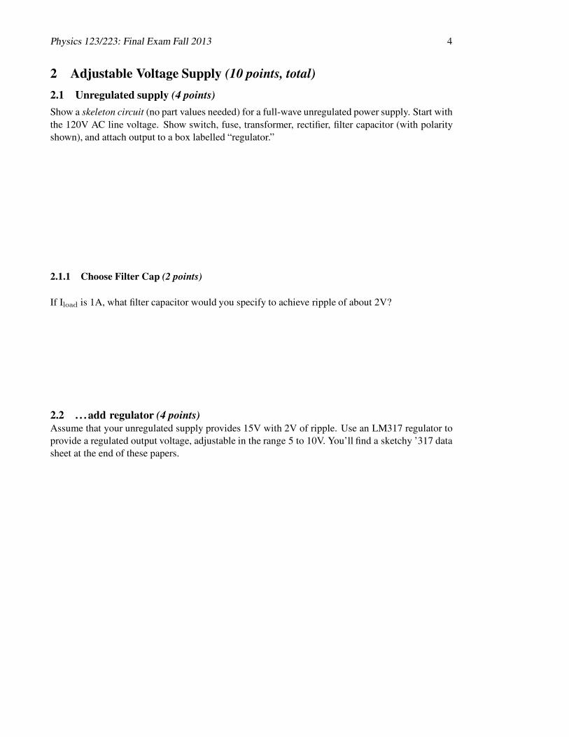
Show a skeleton circuit (no part values needed) for a full-wave unregulated power supply. Start withthe 120V AC line voltage. Show switch, fuse, transformer, rectifier, filter capacitor (with polarityshown), and attach output to a box labelled “regulator.”
2.1.1 Choose Filter Cap (2 points)
If Iload is 1A, what filter capacitor would you specify to achieve ripple of about 2V?
2.2 . . . add regulator (4 points)Assume that your unregulated supply provides 15V with 2V of ripple. Use an LM317 regulator toprovide a regulated output voltage, adjustable in the range 5 to 10V. You’ll find a sketchy ’317 datasheet at the end of these papers.

Physics 123/223: Final Exam Fall 2013 5
3 Single-supply Differential Amp (using op amp) (10 points)
Here, we’d like you to design an op-amp-based differential amplifier, to satisfy the following spec-ifications. You can assume an LM358 op amp, the single-supply device you used in some labs.
• power supplies: only +5V
• input range, each of two inputs: 0 to 2.5V
• output range for diff amp: from close to zero1 up to 2.5V (this range accommodates an ADC)
• input impedance: let RIN ≥ 100kΩ
• gain & bias: select the gain, and the quiescent output voltage (i.e., output when input voltages are equal) so thatthe full range of allowable inputs yields the full range of allowable output voltages, without saturation.
1Low end of range limited by output swing of single-supply op amp; 20mV for LM358 sinking 20µA, typical, forexample.

Physics 123/223: Final Exam Fall 2013 6
4 Logic Probe (12 points, total)4.1 Simple: High-impedance version (8 points)
Design a logic probe, for use with CMOS, to the following specifications. This is a rare case whenyou need not provide hysteresis to stabilize the comparators, since chatter seems harmless in thiscase.
Specifications:
• RIN: 1MΩ
• Logic Thresholds 1/3 and 2/3 of VDD (VDD supply voltage)• Response
– Logic Low: light RED LED;– Logic High: light GREEN LED;– input voltage neither High nor Low: light neither LED; a floating input
should produce the same result: neither LED lit.
The parts you are to use have the following characteristics:
LED wants 5 mA for adequate brightness; drops 2V when lit
comparator TLC371/372: bias current is 500pA, max; the ’371 can sink 5 mA; moreinformation (if you want it) appears in the ’sketchy data sheet’ in appendix tothese exam papers
4.2 Fancy: version that rejects feeble gate drive (4 points)
Now show what changes you would make to your design if your intention were to reject Highs orLows driven by a gate not able to sink or source the current characteristic of a healthy HC gate.
A healthy HC gate can sink or source 4mA, while holding its output within 0.5V of ground orV+, respectively. We are not asking you to alter your circuit’s thresholds to apply this standard:you may keep your logic probe’s thresholds at 1/3 and 2/3 of the supply, as in §4.1. Your probeshould consider a logic level GOOD if it satisfies these thresholds when the driving gate is sinkingor sourcing 4mA.
We assume, incidentally, that the probe is substantially the only load applied to the gate that it tests.
Physics 123/223: Final Exam Fall 2013 7
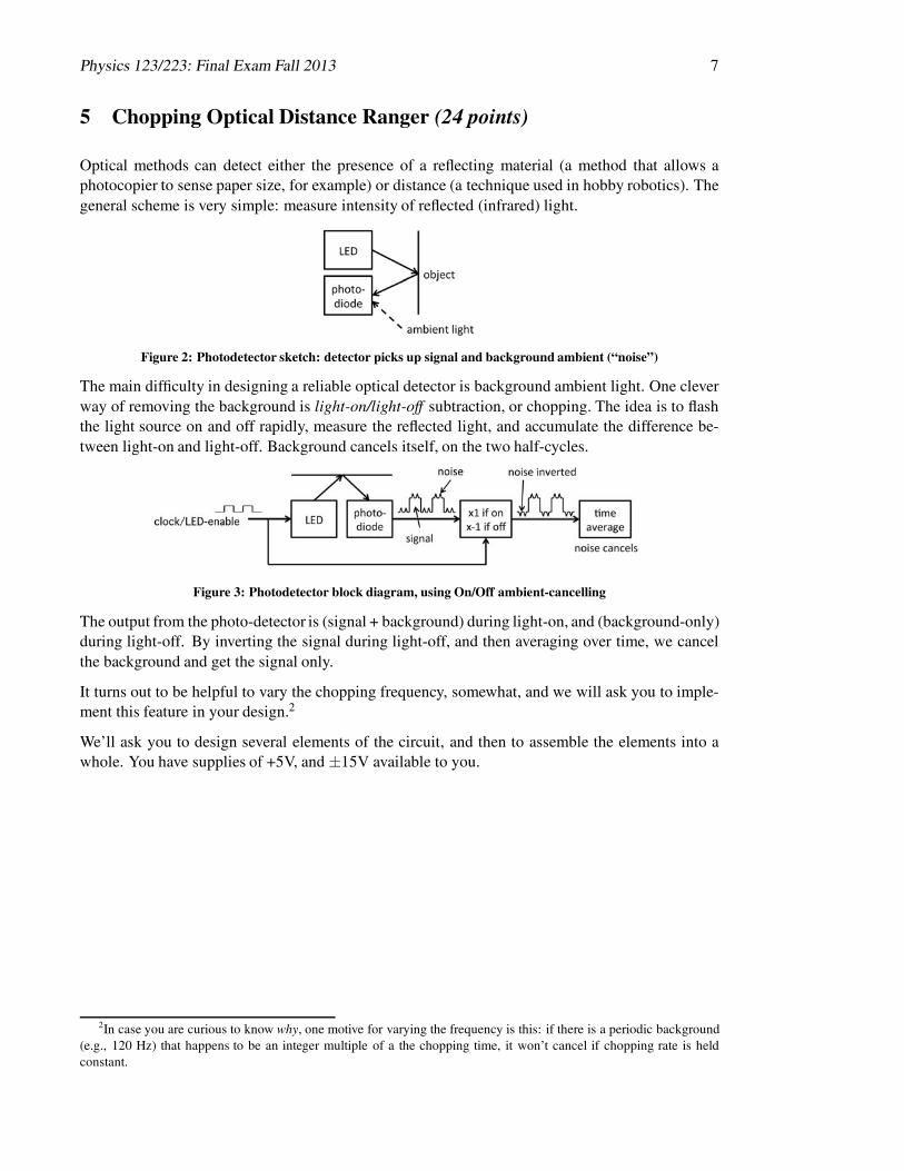
5 Chopping Optical Distance Ranger (24 points)
Optical methods can detect either the presence of a reflecting material (a method that allows aphotocopier to sense paper size, for example) or distance (a technique used in hobby robotics). Thegeneral scheme is very simple: measure intensity of reflected (infrared) light.
Figure 2: Photodetector sketch: detector picks up signal and background ambient (“noise”)
The main difficulty in designing a reliable optical detector is background ambient light. One cleverway of removing the background is light-on/light-off subtraction, or chopping. The idea is to flashthe light source on and off rapidly, measure the reflected light, and accumulate the difference be-tween light-on and light-off. Background cancels itself, on the two half-cycles.
Figure 3: Photodetector block diagram, using On/Off ambient-cancelling
The output from the photo-detector is (signal + background) during light-on, and (background-only)during light-off. By inverting the signal during light-off, and then averaging over time, we cancelthe background and get the signal only.
It turns out to be helpful to vary the chopping frequency, somewhat, and we will ask you to imple-ment this feature in your design.2
We’ll ask you to design several elements of the circuit, and then to assemble the elements into awhole. You have supplies of +5V, and ±15V available to you.
2In case you are curious to know why, one motive for varying the frequency is this: if there is a periodic background(e.g., 120 Hz) that happens to be an integer multiple of a the chopping time, it won’t cancel if chopping rate is heldconstant.
Physics 123/223: Final Exam Fall 2013 8
5.1 Oscillator (10 points)
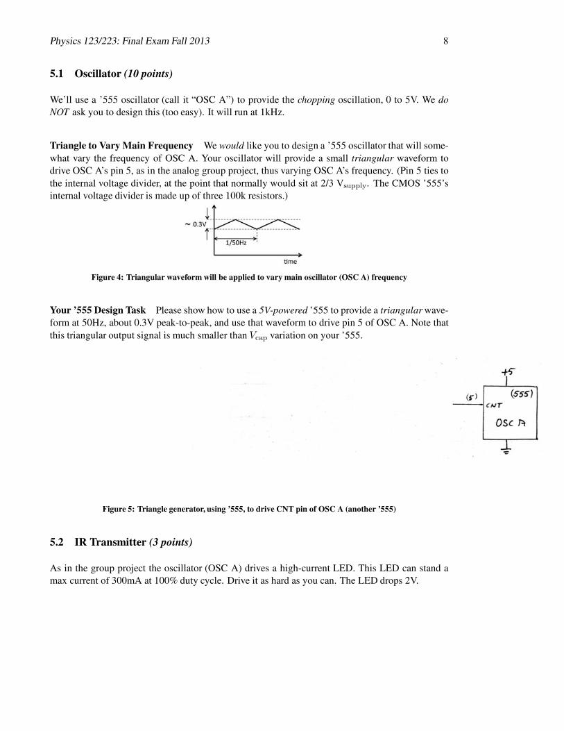
We’ll use a ’555 oscillator (call it “OSC A”) to provide the chopping oscillation, 0 to 5V. We doNOT ask you to design this (too easy). It will run at 1kHz.
Triangle to Vary Main Frequency We would like you to design a ’555 oscillator that will some-what vary the frequency of OSC A. Your oscillator will provide a small triangular waveform todrive OSC A’s pin 5, as in the analog group project, thus varying OSC A’s frequency. (Pin 5 ties tothe internal voltage divider, at the point that normally would sit at 2/3 Vsupply. The CMOS ’555’sinternal voltage divider is made up of three 100k resistors.)
Figure 4: Triangular waveform will be applied to vary main oscillator (OSC A) frequency
Your ’555 Design Task Please show how to use a 5V-powered ’555 to provide a triangular wave-form at 50Hz, about 0.3V peak-to-peak, and use that waveform to drive pin 5 of OSC A. Note thatthis triangular output signal is much smaller than Vcap variation on your ’555.
Figure 5: Triangle generator, using ’555, to drive CNT pin of OSC A (another ’555)
5.2 IR Transmitter (3 points)
As in the group project the oscillator (OSC A) drives a high-current LED. This LED can stand amax current of 300mA at 100% duty cycle. Drive it as hard as you can. The LED drops 2V.
Physics 123/223: Final Exam Fall 2013 9
5.3 Detector (4 points)
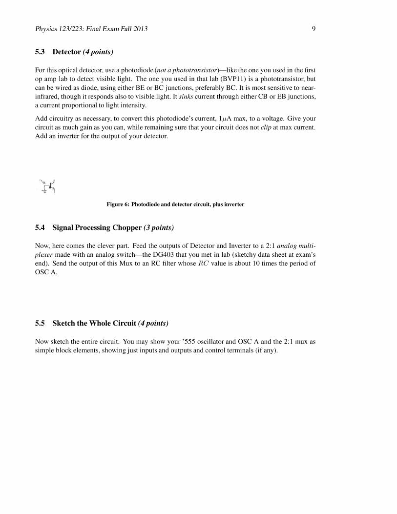
For this optical detector, use a photodiode (not a phototransistor)—like the one you used in the firstop amp lab to detect visible light. The one you used in that lab (BVP11) is a phototransistor, butcan be wired as diode, using either BE or BC junctions, preferably BC. It is most sensitive to near-infrared, though it responds also to visible light. It sinks current through either CB or EB junctions,a current proportional to light intensity.
Add circuitry as necessary, to convert this photodiode’s current, 1µA max, to a voltage. Give yourcircuit as much gain as you can, while remaining sure that your circuit does not clip at max current.Add an inverter for the output of your detector.
Figure 6: Photodiode and detector circuit, plus inverter
5.4 Signal Processing Chopper (3 points)
Now, here comes the clever part. Feed the outputs of Detector and Inverter to a 2:1 analog multi-plexer made with an analog switch—the DG403 that you met in lab (sketchy data sheet at exam’send). Send the output of this Mux to an RC filter whose RC value is about 10 times the period ofOSC A.
5.5 Sketch the Whole Circuit (4 points)
Now sketch the entire circuit. You may show your ’555 oscillator and OSC A and the 2:1 mux assimple block elements, showing just inputs and outputs and control terminals (if any).
Physics 123/223: Final Exam Fall 2013 10
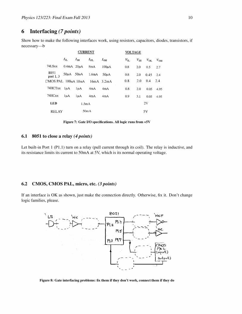
6 Interfacing (7 points)
Show how to make the following interfaces work, using resistors, capacitors, diodes, transistors, ifnecessary—but no op amps or comparators.
Figure 7: Gate I/O specifications. All logic runs from +5V
6.1 8051 to close a relay (4 points)
Let built-in Port 1 (P1.1) turn on a relay (pull current through its coil). The relay is inductive, andits resistance limits its current to 50mA at 5V, which is its normal operating voltage.
6.2 CMOS, CMOS PAL, micro, etc. (3 points)
If an interface is OK as shown, just make the connection directly. Otherwise, fix it. Don’t changelogic families, please.
Figure 8: Gate interfacing problems: fix them if they don’t work, connect them if they do
Physics 123/223: Final Exam Fall 2013 11
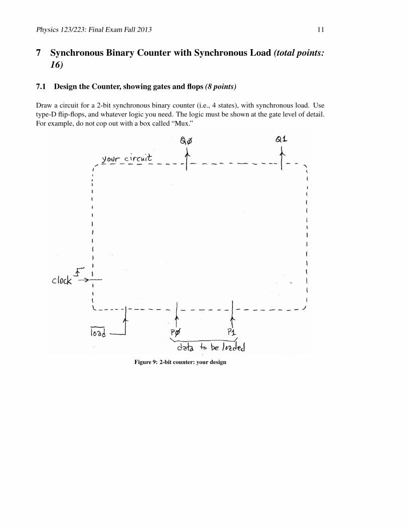
7 Synchronous Binary Counter with Synchronous Load (total points:16)
7.1 Design the Counter, showing gates and flops (8 points)
Draw a circuit for a 2-bit synchronous binary counter (i.e., 4 states), with synchronous load. Usetype-D flip-flops, and whatever logic you need. The logic must be shown at the gate level of detail.For example, do not cop out with a box called “Mux.”
Figure 9: 2-bit counter: your design
Physics 123/223: Final Exam Fall 2013 12
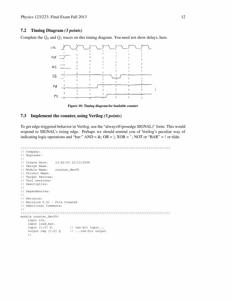
7.2 Timing Diagram (3 points)
Complete the Q0 and Q1 traces on this timing diagram. You need not show delays, here.
Figure 10: Timing diagram for loadable counter
7.3 Implement the counter, using Verilog (5 points)
To get edge-triggered behavior in Verilog, use the “always@(posedge SIGNAL)” form. This wouldrespond to SIGNAL’s rising edge. Perhaps we should remind you of Verilog’s peculiar way ofindicating logic operations and “bar:” AND = &; OR = |; XOR = ˆ ; NOT or “BAR” = ! or tilde.
//////////////////////////////////////////////////////////////////////////////////// Company:// Engineer://// Create Date: 13:40:03 12/13/2009// Design Name:// Module Name: counter_dec09// Project Name:// Target Devices:// Tool versions:// Description://// Dependencies://// Revision:// Revision 0.01 - File Created// Additional Comments:////////////////////////////////////////////////////////////////////////////////////module counter_dec09(
input clk,input load_bar,input [1:0] P, // two-bit input...output reg [1:0] Q // ...two-bit output);

Physics 123/223: Final Exam Fall 2013 13
8 Sampling (13 pts)
A telephone answering machine doesn’t need excellent sound quality, because the original tele-phone signal is pretty crummy.3 Telephone signals carry no information above about 3kHz, and theamplitude “fidelity” or accuracy doesn’t have to be very good. Here, we’d like you to help specifyan ADC converter for an answering machine that is to store phone messages in digital form, thenplay them out through a DAC.
8.1 Number of Bits (3 pts)
In order to resolve the signal amplitude to ±1% of full-scale , how many bits are required? Thefigure below, fig.11, reminds us that amplitude is not the same as “peak-to-peak” amplitude.
Figure 11: What “amplitude” of an analog signal means
8.2 Sampling Rate (8 pts)
What sampling rate do you recommend? Assume that the output filter, used to smooth the recoveredanalog signal, is “steep” enough to reduce amplitude by a factor of at least 100 for frequencies 20%above the “cutoff” frequency, or f3dB. Take no more samples than you need. Explain your choice,briefly.
8.3 Unexpected Noise (2 pts)
If your circuit includes no anti-aliasing filter, and strong electrical noise appears at the ADC input,at about 5kHz, will this noise be eliminated by your reconstruction filter (that is, a low-pass filterapplied to the DAC output)? Please give a quantitative argument to support your answer.
3Also known as “crumby.”
Physics 123/223: Final Exam Fall 2013 14
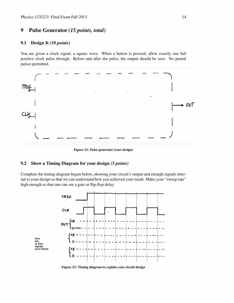
9 Pulse Generator (15 points, total)
9.1 Design It (10 points)
You are given a clock signal, a square wave. When a button is pressed, allow exactly one fullpositive clock pulse through. Before and after the pulse, the output should be zero. No partialpulses permitted.
Figure 12: Pulse generator (your design)
9.2 Show a Timing Diagram for your design (5 points)
Complete the timing diagram begun below, showing your circuit’s output and enough signals inter-nal to your design so that we can understand how you achieved your result. Make your “sweep rate”high enough so that one can see a gate or flip-flop delay.
Figure 13: Timing diagram to explain your circuit design

Physics 123/223: Final Exam Fall 2013 15
Micro Question: Inverted Pendulum
The goal, here, is to make a start on the design of an inverted-pendulum machine—one of theperennial heartbreakers among Physics 123 projects. We will dodge the real difficulties—the onesthat have defeated most students in “real” (lab-) life: the stability problems. But we’ll make a starton setting up sensors and letting a microcontroller take in that information.
10 I/O Decode (17 pts, total of those shown below)
We would like you to show I/O decoding for this controller, slightly different from what we used inthe lab microcomputer. Again, I/O goes high in address space, but occupying only 1K of addressspace at the very top. (This scheme would make sense if we used a larger RAM: 64K rather than the32K that we use in lab; the smaller I/O space would leave 63K of RAM usable. We are not askingyou to work out how RAM would be disabled in this top 1K of address space.)
10.1 What Hex Address? (2 pts)
What is the hexadecimal address of PORT0, given your decoding? As in the lab computer, PORT0,1 and 2 are offset by 0, 1 and 2 from the beginning of I/O space. (And note that this external-busPORT0 is not the same as the port zero that is one of the 8051’s built-in ports.)
10.2 Draw decoding with Gates (8 pts)
Show how to decode the following ports, using gates (not a decoder IC), to produce the 5 enablingsignals below (all active-low):
• out0*• in1*, out1*• in2*, out2*
You can save yourself some writing effort if you define some preliminary functions that your severaldecoded lines can share—for example, a signal named “io.” You’ll see such preliminary signalssuggested also in the template files for Verilog implementation of this decoding task (§ 10.3 on thefollowing page).

Physics 123/223: Final Exam Fall 2013 16
10.3 Decode using Verilog (7 pts)
Use Verilog to do the same decoding task.
In order to refer to a particular address line—for example, address line 12—write “A[12]”.
//////////////////////////////////////////////////////////////////////////////////module address_decode_final10(
input RD_bar,input WR_bar,input [15:0] A, // 16-line address busoutput out0_bar,output in1_bar,output out1_bar,output in2_bar,output out2_bar);
// the next five lines are not required, but may save you some repetitive writing: your later// assignments could re-use the signals listed here, if you like
wire io, port0, port1, port2;
assign io =
assign port0 =
assign port1 =
assign port2 =
//------------
assign out0_bar =
assign in1_bar =
assign out1_bar =
assign in2_bar =
assign out2_bar =
endmodule

Physics 123/223: Final Exam Fall 2013 17
11 Sensor and Motor-drive Hardware and Code (25 pts, total of severalsubsections)
In this question we ask you to set up some hardware and write some code that could begin theinverted pendulum project. But you don’t need to understand the pendulum project in order toanswer the question, which asks you to let the microcontroller take in four sensor values and drivea DC motor. We provide a brief sketch of the arrangement we have in mind, in case you want somemotivation to do this task. But at exam time, you may prefer to race on, scorning words that mightprovide “motivation.” You may already feel sufficiently motivated.
A description of the scheme we propose: Accelerometers to sense Tilt The computer can sense thetilt of a meter stick using a two-axis accelerometer (the axes at right angles), plus one more accelerometer thatsenses left-right acceleration. We could set it up as on the left, in fig.14. We’d like one more item of information: avoltage input from a ten-turn potentiometer, measuring the left-right position (not acceleration). This informationlets the balancer drive the mechanism toward the center if it wanders too close to one of its limits.The overall scheme is sketched on the right, in fig.14.
Figure 14: Tilt-sensing accelerometers: X, Y, and H (horizontal acceleration)
We will call the three accelerometer readings “X, Y, H,” and the position reading “P.”
Nothing for you to do, on this page. Your work begins on the next page.
Physics 123/223: Final Exam Fall 2013 18
11.1 Hardware (15 pts, total of two subsections)
11.1.1 Hardware to Let the Controller Get Sensor Readings (9 pts)
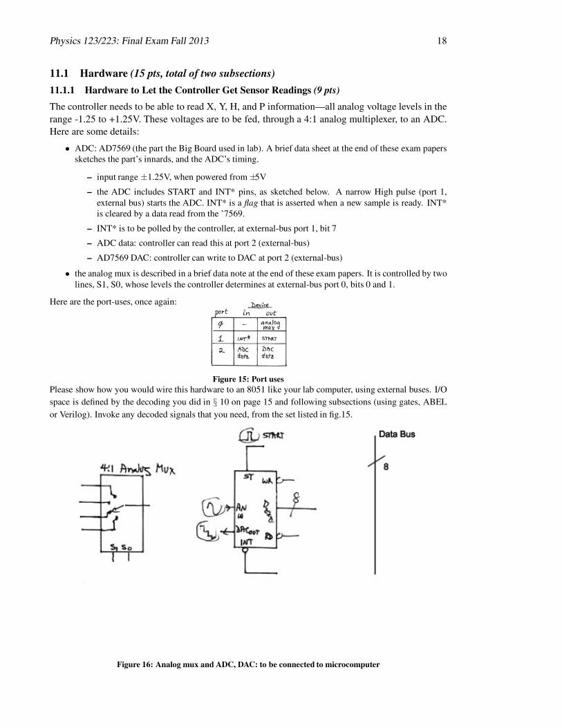
The controller needs to be able to read X, Y, H, and P information—all analog voltage levels in therange -1.25 to +1.25V. These voltages are to be fed, through a 4:1 analog multiplexer, to an ADC.Here are some details:
• ADC: AD7569 (the part the Big Board used in lab). A brief data sheet at the end of these exam paperssketches the part’s innards, and the ADC’s timing.
– input range ±1.25V, when powered from ±5V
– the ADC includes START and INT* pins, as sketched below. A narrow High pulse (port 1,external bus) starts the ADC. INT* is a flag that is asserted when a new sample is ready. INT*is cleared by a data read from the ’7569.
– INT* is to be polled by the controller, at external-bus port 1, bit 7
– ADC data: controller can read this at port 2 (external-bus)
– AD7569 DAC: controller can write to DAC at port 2 (external-bus)
• the analog mux is described in a brief data note at the end of these exam papers. It is controlled by twolines, S1, S0, whose levels the controller determines at external-bus port 0, bits 0 and 1.
Here are the port-uses, once again:
Figure 15: Port usesPlease show how you would wire this hardware to an 8051 like your lab computer, using external buses. I/Ospace is defined by the decoding you did in § 10 on page 15 and following subsections (using gates, ABELor Verilog). Invoke any decoded signals that you need, from the set listed in fig.15.
Figure 16: Analog mux and ADC, DAC: to be connected to microcomputer

Physics 123/223: Final Exam Fall 2013 19
11.1.2 Motor Drive Hardware (6 pts)
Show circuitry that will allow the ’7569’s DAC (output range ±1.25V) to drive the printer’s DCmotor, which draws up to 1A at ±10V, full-scale. You are given power supplies of ±15V. Includeprotections against parasitic oscillations.
11.2 Code: Subroutine Getsample (10 pts, total)
We would like you to write one subroutine that a main program will invoke:
This is a subroutine that starts the ADC and takes in a sample when one is ready. This sample valueis to be carried in register A, the accumulator (to be read from register A by the calling program onreturn from this subroutine).
Here are some details and reminders:
• this routine, like any polite subroutine, should save any registers that it messes up (but note that re-turning the sample is not what we’d call “messing up” a register!).
• Port use reminder:– Port 0: analog mux– Port 1: Start and INT*– Port 2: ADC data
End Exam Questions: Appendix follows123final dec13.tex; December 14, 2013
Physics 123/223: Final Exam Fall 2013 20
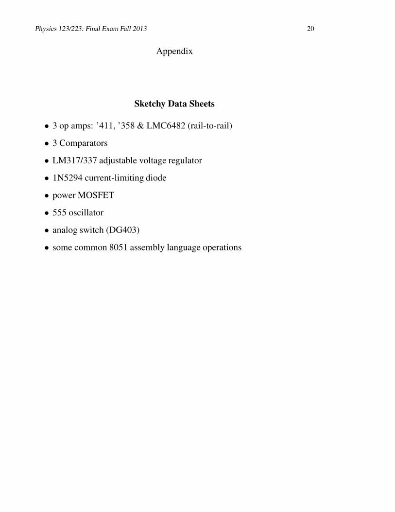
Appendix
Sketchy Data Sheets
• 3 op amps: ’411, ’358 & LMC6482 (rail-to-rail)
• 3 Comparators
• LM317/337 adjustable voltage regulator
• 1N5294 current-limiting diode
• power MOSFET
• 555 oscillator
• analog switch (DG403)
• some common 8051 assembly language operations

Physics 123/223: Final Exam Fall 2013 21
(Very-) Abbreviated Data Sheets
Figure 17: 3 Op Amps
Figure 18: Three Comparators

Physics 123/223: Final Exam Fall 2013 22
Figure 19: LM317/337 adjustable voltage regulator
Figure 20: 1N5294 Current Limiting Diode: Sketchy Data Sheet
Figure 21: Power MOSFETs: Sketchy Data Sheet

Physics 123/223: Final Exam Fall 2013 23
Figure 22: 555 Sketchy Data Sheet
Figure 23: Analog Switch: Sketchy Data Sheet
[END WHOLE EXAM PAPER, except 2 pages re common 8051 operations]
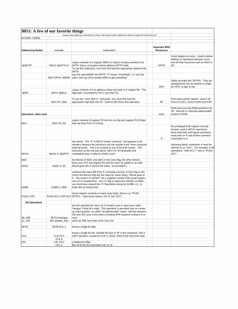
8051: A few of our favorite thingsinspired (one might say, 'shamed') by Carlos, who wrote another, better list--which we hope he'll share with you
5/7/2004, 12/8/05
Addressing Modes example explanationImportant 8051
Resources
"@DPTR" "MOVX @DPTR,A"copies contents of A register (8051 on-chip) to location pointed to by DPTR: that is, to location whose address DPTR holds DPTR
16-bit register on micro. Used to define address of operations between micro and off-chip resources such as RAM or I/O.
To use this instruction, one must first load the appropriate address into DPTR
MOV DPTR, #8003hputs the value 8003h into DPTR: "#" means "immediate," or "use this value; don't go off to location 8003 to get something"
DPS
Dallas provides two DPTRS. They are distinguished only by whether a single bit, DPS, is high or low.
"@R0" MOVX @R0,Acopies contents of A to address whose low-byte is in register R0. The high-byte is provided by Port 2 (on-chip P2).
MOV P2, #80hTo use the `movx @r0,a" instruction, one must first load the appropriate high-byte into P2. Code to left shows that operation. SP
8-bit stack pointer register: used in all forms of CALL, and in PUSH and POP
Operations often used stack
RAM area (on-chip RAM) pointed to by SP. Must be in 'indirectly-addressable' section of RAM.
MOV MOV P2, R3copies contents of register R3 into the on-chip port register P2 (8 flops that can drive Port 2's 8 lines)
A
the privileged 8-bit register: the only location used in MOVX operations. Most arithmetic and logical operations must work on A and another operand; result goes to A.
MOVX MOVX A, @DPTR
see above. The "X" in MOVX means "external," and appears in all transfers between the processor and the outside world, when using the external buses . This is in contrast to use of the built-in ports . The instruction on the line just above, MOV P2, R3 illustrates that contrasting case: a write to a built-in port.
Annoying detail: sometimes A must be referred to as "ACC". For example, in bitoperations: "JNB ACC.7" and in "PUSH ACC."
ADD two flavors of ADD: one takes in the Carry flag, the other doesn't.
ADDC ADDC A, R2forms sum of A and register R2 and the Carry bit (added in at LSB). Result goes into A (hence the name, "accumulator").
SUBB SUBB A, #80h
subtracts the value 80h from A--including a borrow if Carry flag is set. (Carry and Borrow flag are the same bit: same thing.) Result goes to A. The result in A will NOT be a negative number (that would require use of 2's-complement). Use CY flag to determine whether A<#80h--you must have cleared the CY flag before doing the SUBB, n.b., to make this an honest test.
PUSH, POP PUSH ACC, POP ACCstores register contents on stack (only bytes: there is no "PUSH DPTR") . Note funny names: not "A" but "ACC".
Bit Operations
JB, JNB JB P3.4,hangup
test the specified bit--here, bit 4 of built-in port 3--and hop to label "hangup" if that bit is High. This operation is permitted only on certain on-chip locations: so-called "bit-addressable" region, 128 bits between 20h and 2Fh, plus a few others including SFR locations ending in 8 or zero!.
JC, JNC JNC greater_than same as JNB, but looks at the Carry bit
SETB SETB ACC.1 forces a single bit high
CLR CLR P3.0forces a single bit low. Despite the lack of "B" in the mnemonic, this is a BIT operation, except for CLR A, which I think is the only 8-bit clear.
CLR ACPL CPL P3.1 complement (flip)
CPL A flips all 8 bits (but permitted only on A)
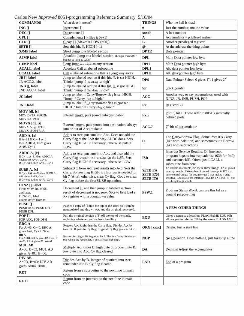
Carlos New Improved 8051-programming Reference Summary 5/18/04 COMMANDS What does it mean? THINGS Who the hell is that? INC [] Increments [] # Just the number, not the value DEC [] Decrements [] xxxxh A hex number CPL [] Complements [] (flips it 0↔1) A Accumulator = privileged register CLR [] Clears [] (Makes it LOW (=00)) B Another privileged register SETB [] Sets this bit, [], HIGH (=1) @ At the address the thing points SJMP label Short Jump to a labeled section DPTR Data pointer
AJMP label Absolute Jump to a labeled section. (Longer than SJMP but not as long as LJMP) DPL Main Data pointer low byte
LJMP label Long Jump (the longest) to any section DPH Main Data pointer high byte ACALL label Absolute Call a labeled subroutine DPL1 Alt. data pointer low byte LCALL label Call a labeled subroutine that’s a long way away DPH1 Alt. data pointer high byte JB [], label JB ACC.2, label
Jump to labeled section if this bit, [], is set HIGH. Think: “jump if (this thing is) high” DPS Data Pointer Select; 0 gives 1st, 1 gives 2nd
JNB [], label JNB ACC.4, label
Jump to labeled section if this bit, [], is not HIGH. Think: “jump if (this thing is) low” SP Stack pointer
JC label Jump to label if Carry/Borrow flag is set HIGH. “Jump if Carry (flag is) high.” ACC Another way to say accumulator, used with
DJNZ, JB, JNB, PUSH, POP
JNC label Jump to label if Carry/Borrow flag is Not set HIGH. “Jump if Carry (flag is) low.” Rx Register 0-7
MOV [d], [s] MOV DPTR, #8002h MOV R3, #93h
Internal move, puts source into destination Px.x Port 3, bit 1. These refer to 8051’s internally defined ports
MOVX [d], [s] MOVX A, @DPTR MOVX @DPTR, A
External move, puts source into destination, always into or out of Accumulator ACC.7 7th bit of accumulator
ADD A, [x] if A=81 & Cy=1 or 0 then ADD A, #82h gives A=03, Cy=1
Add x to Acc, put sum into Acc. Does not add the Carry flag at the LSB the way ADDC does. Sets Carry flag HIGH if necessary, otherwise puts it LOW.
C The Carry/Borrow Flag. Sometimes it’s Carry (like with Addition) and sometimes it’s Borrow (like with subtraction)
ADDC A, [x] If Cy=1, A=81 then ADDC A, #82h gives A=04, Cy=1. If Cy was 0, then A=03, Cy=1
Add x to Acc, put sum into Acc, and also add the Carry flag (whether HIGH or LOW) at the LSB. Sets Carry flag HIGH if necessary, otherwise LOW.
ISR
Interrupt Service Routine. On interrupt, program hops to interrupt address (03h for Int0) and executes ISR. Often, just LCALL a subroutine from here.
SUBB A, [x] If Cy is 0 & A=72 then SUBB A, #81 gives A=F1, Cy=1. If Cy was 1, then A=F1, Cy=0
Subtract x from Acc, put results into Acc. Sets the Carry/Borrow flag HIGH if a Borrow is needed for bit 7 (A<x), otherwise, clear Cy flag. Good to clear Cy flag before the first SUBB operation.
SETB EA SETB EX0 SETB IT0
To enable interrupts, do these three things. EA is global interrupt enable. EX0 enables External Interrupt 0. IT0 is a timer control thingy for ext. interrupt 0 that makes it edge sensitive. Could also use interrupt 1 (SETB EX1 and IT1) but let’s keep things simple
DJNZ [], label First: MOV R6, #06h and later: DJNZ R6, label counts down from 06
Decrement [], and then jump to labeled section if result of decrement is not zero. Nice to first load a Rx register with a countdown value
PSW.1 Program Status Word, can use this bit as a general purpose flag
PUSH [] PUSH ACC, PUSH DPH PUSH DPL
Pushes a copy of [] onto the top of the stack so it can be manipulated and thrown out, and the original recovered. A FEW OTHER THINGS
POP [] POP ACC, POP DPH
Pull the original version of [] off the top of the stack, replacing whatever you’ve been handling EQU Gives a name to a location. FLAGNAME EQU 05h
allows you to refer to 05h by the name FLAGNAME RRC A For A=05, Cy=0, RRC A gives A=2, Cy=1. Nice.
Rotates Acc Right thru the Carry flag. Divides Acc by two. Bit 0 goes to Cy flag; original Cy flag goes to bit 7. ORG [xxxx] Origin. Just a start line
RR A For A=04, RR A gives 02. Fine. If A=03, RR A gives 81. Weird.
Rotates Acc Right. Bit 0 goes to bit 7. This is a funny divide-by-two where the remainder, if any, affects high digit. NOP No Operation. Does nothing, just takes up a line
MUL AB A=06, B=02; MUL AB gives A=0C, B=00.
Multiply Acc times B, high byte of product into B, low byte into Acc. Cy flag cleared. DA Decimal Adjust the accumulator
DIV AB A=0D, B=03; DIV AB gives A=04, B=01.
Divides Acc by B. Integer of quotient into Acc, remainder into B. Cy flag cleared. END End of a program
RET Return from a subroutine to the next line in main code
RETI Return from an interrupt to the next line in main code