Embed Size (px)
DESCRIPTION
Physical Limits of Computing Dr. Mike Frank CIS 6930, Sec. #3753X Spring 2002. Lecture #23 Adiabatic Electronics & CMOS Mon., Mar. 11. Administrivia & Overview. Don’t forget to keep up with homework! We are 7 out of 14 weeks into the course. You should have earned ~ 50 points by now. - PowerPoint PPT Presentation
Citation preview
Physical Limits of ComputingPhysical Limits of ComputingDr. Mike FrankDr. Mike Frank
CIS 6930, Sec. #3753X CIS 6930, Sec. #3753XSpring 2002Spring 2002
Lecture #23Lecture #23Adiabatic Electronics & CMOS Adiabatic Electronics & CMOS
Mon., Mar. 11Mon., Mar. 11
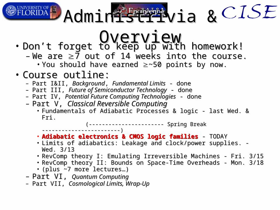
Administrivia & OverviewAdministrivia & Overview• Don’t forget to keep up with homework!Don’t forget to keep up with homework!
– We are We are 7 out of 14 weeks into the course.7 out of 14 weeks into the course.• You should have earned You should have earned ~50 points by now.~50 points by now.
• Course outline:Course outline:– Part I&II, Part I&II, BackgroundBackground, , Fundamental LimitsFundamental Limits - done - done– Part III, Part III, Future of Semiconductor TechnologyFuture of Semiconductor Technology - done - done– Part IV, Part IV, Potential Future Computing TechnologiesPotential Future Computing Technologies - done - done– Part V, Part V, Classical Reversible ComputingClassical Reversible Computing
• Fundamentals of Adiabatic Processes & logic - last Wed. & Fri.Fundamentals of Adiabatic Processes & logic - last Wed. & Fri.(----------------------- Spring Break ------------------------)(----------------------- Spring Break ------------------------)
• Adiabatic electronics & CMOS logic familiesAdiabatic electronics & CMOS logic families - TODAY - TODAY• Limits of adiabatics: Leakage and clock/power supplies. - Wed. 3/13Limits of adiabatics: Leakage and clock/power supplies. - Wed. 3/13• RevComp theory I: Emulating Irreversible Machines - Fri. 3/15RevComp theory I: Emulating Irreversible Machines - Fri. 3/15• RevComp theory II: Bounds on Space-Time Overheads - Mon. 3/18RevComp theory II: Bounds on Space-Time Overheads - Mon. 3/18• (plus ~7 more lectures…)(plus ~7 more lectures…)
– Part VI, Part VI, Quantum ComputingQuantum Computing– Part VII, Part VII, Cosmological Limits, Wrap-UpCosmological Limits, Wrap-Up
Adiabatic electronics & Adiabatic electronics & CMOS implementationsCMOS implementations

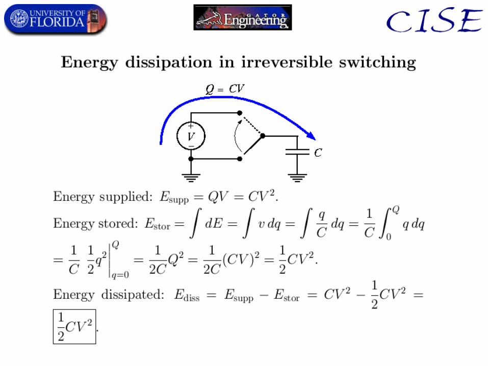
Conventional Gates are IrreversibleConventional Gates are Irreversible• Logic gate behavior (on receiving new input):Logic gate behavior (on receiving new input):
– Many-to-one transformation of local state!Many-to-one transformation of local state!– Required to dissipate bRequired to dissipate bTT by Landauer principle by Landauer principle– Incurs ½Incurs ½CVCV22 dissipation in 2 out of 4 cases. dissipation in 2 out of 4 cases.
Just beforetransition:
Aftertransition:
in out in out0 00 1 0 11 0 1 01 1
in out
Example:
Static CMOS Inverter:
Transformation of local state:
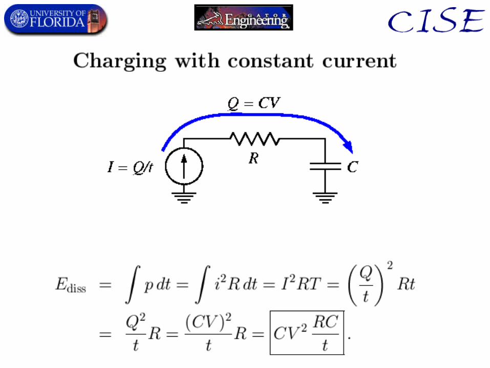
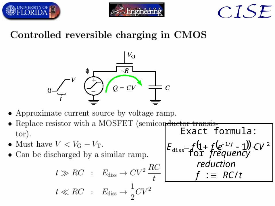
Exact formula:
for frequency reduction f : RC/t
2/1diss 11 CVeffE f


Adiabatic Rules for TransistorsAdiabatic Rules for Transistors• Rule 1: Rule 1: Never turn Never turn onon a transistor if it has a nonzero a transistor if it has a nonzero
voltage across it!voltage across it!– I.e.I.e., between its source & drain terminals., between its source & drain terminals.– Why:Why: This erases info. & causes ½ This erases info. & causes ½CVCV22 disspation. disspation.
• Rule 2:Rule 2: Never apply a nonzero voltage across a Never apply a nonzero voltage across a transistor even transistor even duringduring any on any onoff transition!off transition!– Why: Why: When partially turned on, the transistor has When partially turned on, the transistor has
relatively low relatively low RR, gets high , gets high PP==VV22//RR dissipation. dissipation.– Corollary:Corollary: Never turn Never turn offoff a transistor if it has a nonzero a transistor if it has a nonzero
current going through it!current going through it!• Why: Why: As As RR gradually increases, the gradually increases, the VV==IRIR voltage drop will voltage drop will
build, and then rule 2 will be violated.build, and then rule 2 will be violated.

Adiabatic Rules continuedAdiabatic Rules continued• Transistor Rule 3:Transistor Rule 3: Never suddenly change the Never suddenly change the
voltage applied across any voltage applied across any onon transistor. transistor.– Why:Why: So transition will be more reversible; dissipation So transition will be more reversible; dissipation
will approach will approach CVCV22((RCRC//tt), not ½), not ½CVCV22..
Adiabatic rules for other components:Adiabatic rules for other components:• Diodes: Don’t use them at all!Diodes: Don’t use them at all!
– There is always a built-in voltage drop across them!There is always a built-in voltage drop across them!
• Resistors: Avoid moderate network resistances.Resistors: Avoid moderate network resistances.– e.g.e.g. stay away from range >10 k stay away from range >10 k and <1 M and <1 M
• Capacitors: Minimize, reliability permitting.Capacitors: Minimize, reliability permitting.– Note: Dissipation scales with Note: Dissipation scales with CC22!!
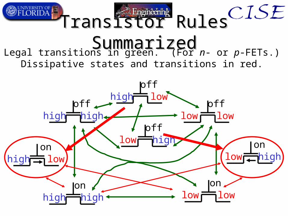
Transistor Rules SummarizedTransistor Rules Summarized
offhigh high
onhigh low
offhigh
offlow low
low
onhigh high
onlow low
Legal transitions in green. (For n- or p-FETs.)Dissipative states and transitions in red.
offhigh low
onhighlow

Just beforetransition:
Aftertransition:
in out in out0 ½ 0 11 ½ 1 0
Transformation of local state:
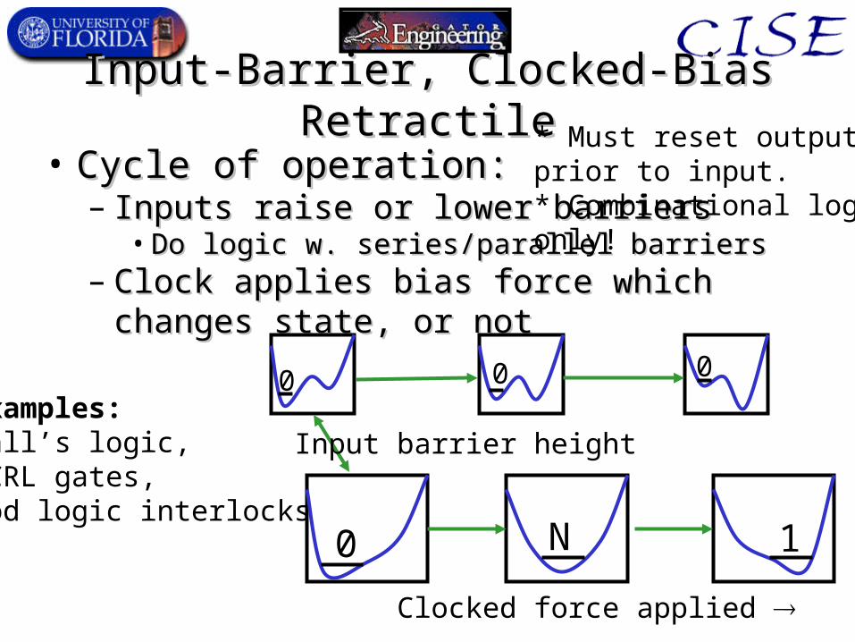
Input-Barrier, Clocked-Bias RetractileInput-Barrier, Clocked-Bias Retractile
• Cycle of operation:Cycle of operation:– Inputs raise or lower barriersInputs raise or lower barriers
• Do logic w. series/parallel barriersDo logic w. series/parallel barriers– Clock applies bias force which changes state, or notClock applies bias force which changes state, or not
0 0 0
10 N
* Must reset outputprior to input.* Combinational logiconly!
Input barrier height
Clocked force applied
Examples:Hall’s logic,SCRL gates,Rod logic interlocks


Retractile Logic w. SCRL gatesRetractile Logic w. SCRL gates• Simple combinational logic of any depth Simple combinational logic of any depth NN::
– Requires Requires NN timing phases timing phases– Non-pipelinedNon-pipelined– No sequential reuse ofNo sequential reuse of
HW (even worse)HW (even worse)
• Sequential logicSequential logicis required!is required!
Time
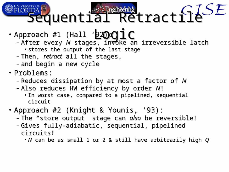
Sequential Retractile LogicSequential Retractile Logic• Approach #1 (Hall ‘92):Approach #1 (Hall ‘92):
– After every After every NN stages, invoke an irreversible latch stages, invoke an irreversible latch• stores the output of the last stagestores the output of the last stage
– Then, Then, retractretract all the stages, all the stages,– and begin a new cycleand begin a new cycle
• Problems:Problems:– Reduces dissipation by at most a factor of Reduces dissipation by at most a factor of NN– Also reduces HW efficiency by order Also reduces HW efficiency by order NN! !
• In worst case, compared to a pipelined, sequential circuitIn worst case, compared to a pipelined, sequential circuit
• Approach #2 (Knight & Younis, ‘93):Approach #2 (Knight & Younis, ‘93):– The “store output” stage can The “store output” stage can alsoalso be reversible! be reversible!– Gives fully-adiabatic, sequential, pipelined circuits!Gives fully-adiabatic, sequential, pipelined circuits!
• NN can be as small 1 or 2 & still have arbitrarily high can be as small 1 or 2 & still have arbitrarily high QQ
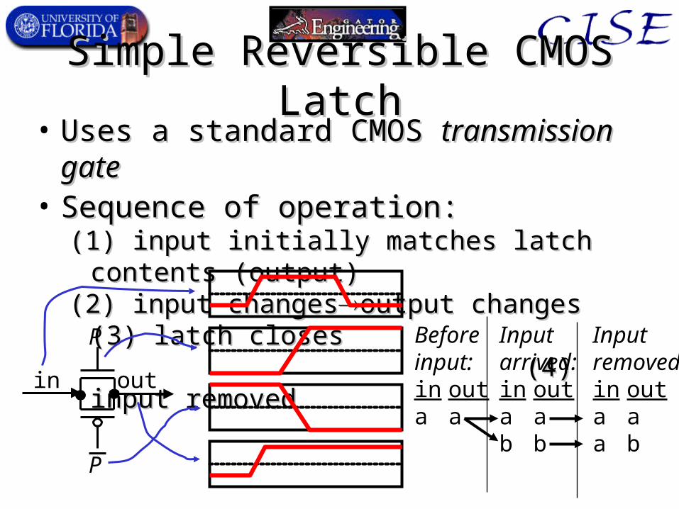
Simple Reversible CMOS LatchSimple Reversible CMOS Latch• Uses a standard CMOS Uses a standard CMOS transmission gatetransmission gate• Sequence of operation:Sequence of operation:
(1) input initially matches latch contents (output)(1) input initially matches latch contents (output)(2) input changes(2) input changesoutput changes (3) latch closesoutput changes (3) latch closes
(4) input (4) input removedremovedP
P
in out
Before Input Inputinput: arrived: removed:in out in out in outa a a a a a
b b a b

Resetting a Reversible LatchResetting a Reversible Latch• Can reversibly Can reversibly unlatchunlatch data as follows: data as follows:
(exactly the reverse of the latching process)(exactly the reverse of the latching process)– (1) Data value (1) Data value dd stored on memory node M. stored on memory node M.– (2) Present an exact copy of (2) Present an exact copy of dd on input. on input.– (3) Open the latch (connecting input to M).(3) Open the latch (connecting input to M).
• No dissipation since voltage levels matchNo dissipation since voltage levels match– (4) Retract the copy of (4) Retract the copy of dd from the input. from the input.
• Retracts copy stored in latch also.Retracts copy stored in latch also.

Input-Bias Clocked-Barrier LogicInput-Bias Clocked-Barrier Logic• Cycle of operation:Cycle of operation:
– Data input applies biasData input applies bias• Add forces to do logicAdd forces to do logic
– Clock signal raises barrierClock signal raises barrier– Data input bias removedData input bias removed
0 0
11
10 N
Input“0”
Input“1”
Retractinput
Retractinput
Clockbarrier
upClock up
Can amplify/restore input signalin clocking step.
Can reset latch reversibly givencopy of contents.
Examples: AdiabaticQDCA, SCRL latch, Rod logic latch, PQ logic,Buckled logic


SCRL 6-tick clock cycleSCRL 6-tick clock cycle
inout
Initial state: All gates off, all nodes neutral.
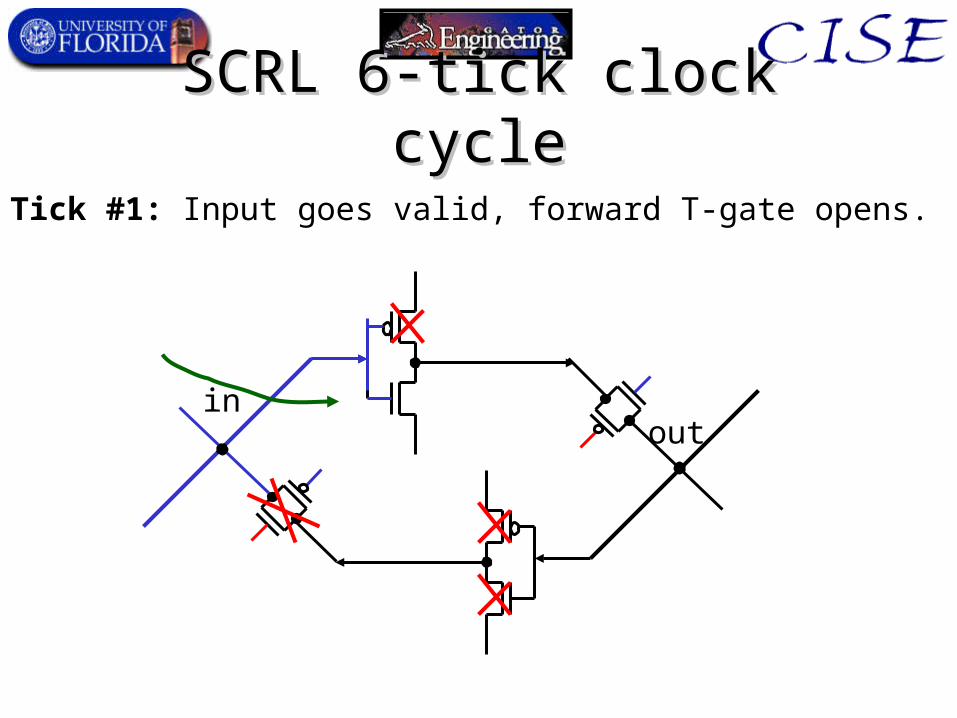
SCRL 6-tick clock cycleSCRL 6-tick clock cycle
inout
Tick #1: Input goes valid, forward T-gate opens.

SCRL 6-tick clock cycleSCRL 6-tick clock cycle
inout
Tick #2: Forward gate charges, output goes valid.(Tick #1 of subsequent gate.)
SCRL 6-tick clock cycleSCRL 6-tick clock cycle
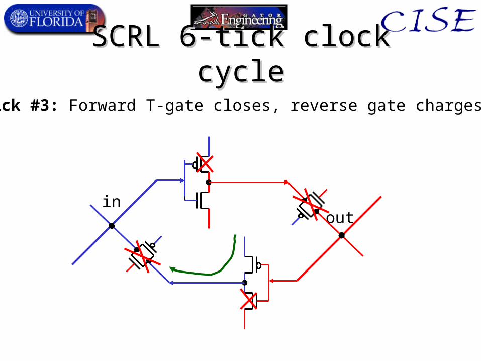
inout
Tick #3: Forward T-gate closes, reverse gate charges.
SCRL 6-tick clock cycleSCRL 6-tick clock cycle
inout
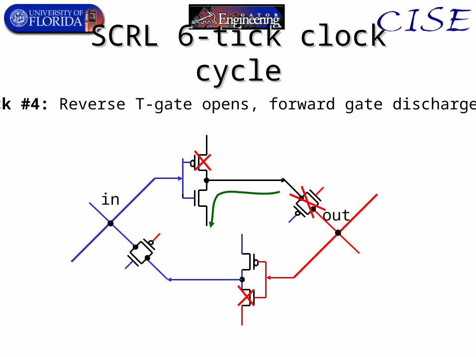
Tick #4: Reverse T-gate opens, forward gate discharges.
SCRL 6-tick clock cycleSCRL 6-tick clock cycle
inout
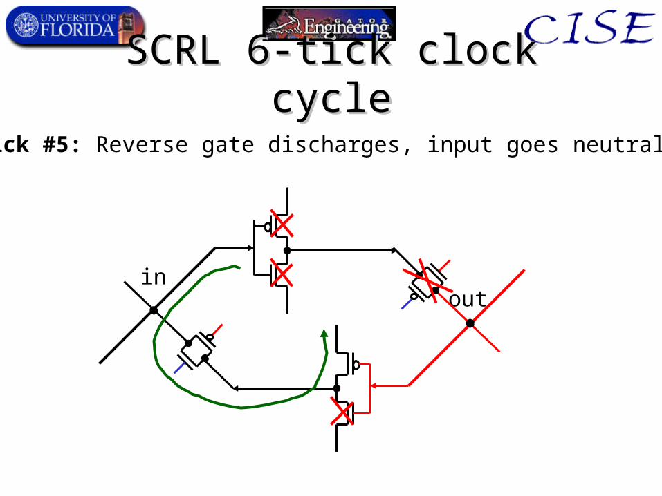
Tick #5: Reverse gate discharges, input goes neutral.

SCRL 6-tick clock cycleSCRL 6-tick clock cycle
inout
Tick #6: Reverse T-gate closes, output goes neutral.Ready for next input!

24 ticks/cyclein this version-includes 2-levelretractile stages

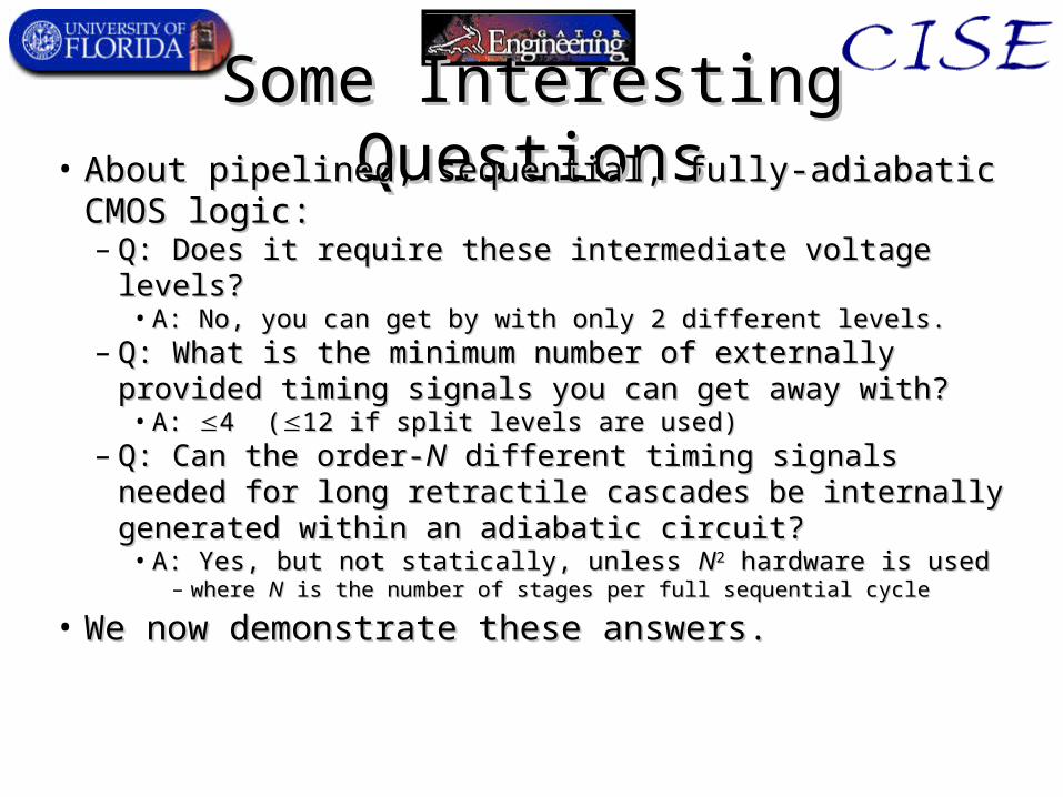
Some Interesting QuestionsSome Interesting Questions• About pipelined, sequential, fully-adiabatic CMOS About pipelined, sequential, fully-adiabatic CMOS
logic:logic:– Q: Does it require these intermediate voltage levels?Q: Does it require these intermediate voltage levels?
• A: No, you can get by with only 2 different levels.A: No, you can get by with only 2 different levels.– Q: What is the minimum number of externally provided Q: What is the minimum number of externally provided
timing signals you can get away with?timing signals you can get away with?• A: A: 4 (4 (12 if split levels are used)12 if split levels are used)
– Q: Can the order-Q: Can the order-NN different timing signals needed for long different timing signals needed for long retractile cascades be internally generated within an adiabatic retractile cascades be internally generated within an adiabatic circuit?circuit?
• A: Yes, but not statically, unless A: Yes, but not statically, unless NN22 hardware is used hardware is used– where where NN is the number of stages per full sequential cycle is the number of stages per full sequential cycle
• We now demonstrate these answers.We now demonstrate these answers.

2LAL: 2-level Adiabatic Logic2LAL: 2-level Adiabatic Logic• Use simplified T-gate symbol:Use simplified T-gate symbol:• Basic buffer element:Basic buffer element:
– cross-coupled T-gatescross-coupled T-gates
• Only 4 timing signals,Only 4 timing signals,4 ticks per cycle:4 ticks per cycle: ii rises during tick rises during tick i i ii falls during tick (( falls during tick ((ii+1) mod 4)+1+1) mod 4)+1
P
P
P
:
in
out
2
1
1 2 3 4Tick #
1
2
3
4

2LAL Cycle of Operation2LAL Cycle of Operation
in
in1
in=0
11
11
20
21
out1
out=0
10
10
in021
out0

Shift Register StructureShift Register Structure• 1-tick delay per logic stage:1-tick delay per logic stage:
• Logic pulse timing & propagation:Logic pulse timing & propagation:
in2
1
3
2
4
3
out
1
4
in
in
1 2 3 4 ... 1 2 3 4 ...

More complex logic functionsMore complex logic functions• Non-inverting Boolean functions:Non-inverting Boolean functions:
• For inverting functions, must use quad-rail logic For inverting functions, must use quad-rail logic encoding:encoding:– To invert, justTo invert, just
swap the rails!swap the rails!• Zero-transistorZero-transistor
“inverters.”“inverters.”
A
B
A
AB
A B
AB
A0
A0
A1
A1
A = 0 A = 1

Hardware Efficiency issuesHardware Efficiency issues• Hardware efficiencyHardware efficiency: How many logic operations : How many logic operations
per unit hardware per unit time?per unit hardware per unit time?• Hardware spacetime complexity:Hardware spacetime complexity: How much How much
hardware for how much time per logic op?hardware for how much time per logic op?• We’re interested in minimizing:We’re interested in minimizing:
(# of transistors) × (# of ticks) / (gate cycle)(# of transistors) × (# of ticks) / (gate cycle)• SCRL inverter, w. return path:SCRL inverter, w. return path:
– (8 transistors) (8 transistors) (6 ticks) = 48 transistor-ticks (6 ticks) = 48 transistor-ticks
• Quad-rail 2LAL buffer stage:Quad-rail 2LAL buffer stage:– (16 transistors) (16 transistors) (4 ticks) = 64 transistor-ticks (4 ticks) = 64 transistor-ticks

More SCRL vs. 2LALMore SCRL vs. 2LAL• SCRL reversible NAND, w. all inverters:SCRL reversible NAND, w. all inverters:
– (23 transistors) (23 transistors) (6 ticks) = 138 T-ticks (6 ticks) = 138 T-ticks
• Quad-rail 2LAL AND:Quad-rail 2LAL AND:– (48 transistors) (48 transistors) (4 ticks) = 192 T-ticks (4 ticks) = 192 T-ticks
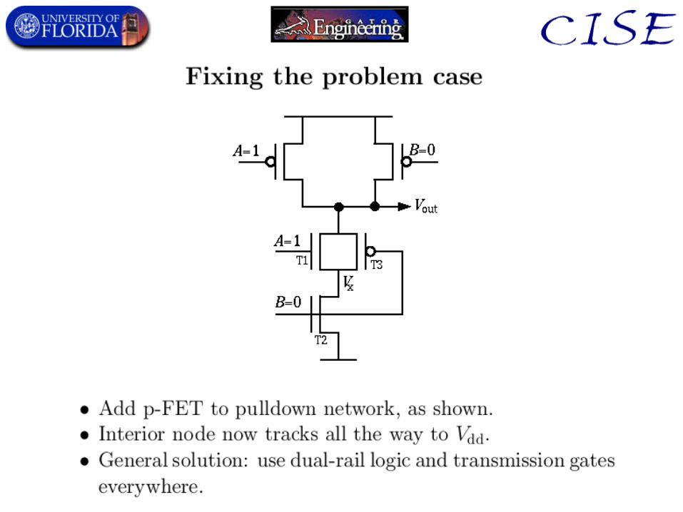
• Result of comparison:Result of comparison: Although 2LAL Although 2LAL minimizes # of rails, and # ticks/cycle, it does minimizes # of rails, and # ticks/cycle, it does notnot minimize overall spacetime complexity.minimize overall spacetime complexity.
• The question of whether 6-tick SCRL minimizes The question of whether 6-tick SCRL minimizes per-op spacetime complexity among pipelined per-op spacetime complexity among pipelined adiabatic CMOS logics is still open.adiabatic CMOS logics is still open.