Embed Size (px)
Citation preview
Photoprocessable Polymer Opals
Birger Lange,† Rudolf Zentel,*,† Christopher Ober,‡ and Seth Marder§
Institute of Organic Chemistry, Department of Chemistry and Pharmacy, University of Mainz,Duesbergweg 10-14, 55128 Mainz, Germany, Department of Materials Science & Engineering,Cornell University, Ithaca, New York 14853, and School of Chemistry and Biochemistry and
Center for Organic Photonics and Electronics, Georgia Institute of Technology,Atlanta, Georgia 30332-0400
Received July 18, 2004. Revised Manuscript Received September 28, 2004
Monodisperse colloids have been synthesized from the acid labile polymer poly tert-butyl-methacrylate. They can be loaded with photoacid generator and crystallized into polymeropal photonic crystals. Irradiation with UV-light followed by baking and development withaqueous base allows subsequent patterning of the opaline films. This chemical approachmakes it possible to use the self-assembly of this colloids (opal formation) to form a large-scale periodic structure and to introduce optical defects with UV-lithography.
Introduction
Progress in electronics and photonics can be seen inthe development of new materials, which broadens ourability to manipulate electron and photon transport,respectively. Photonic crystals (PhCs) are a new classof materials first discussed in 1987. Eli Yablonovitch1
and Sajeev John2 introduced the idea of controlling lightand its emission with photonic crystalline materials.Promising methods for the fabrication of three-dimen-sional (3D) PhCs3 include self-assembly of nanospheresinto opals,4 the use of holography,5 and two-photonlithography.6,7 An important property of PhCs is thatthey have a spatially periodic varying refractive index.This leads to the formation of a photonic band structure,which can possess a complete photonic band gap forcertain frequency ranges. The motivation for researchin this field is to build a generation of optic devices ofreduced size, combining high integration and high-speedprocessing.8
The self-assembly of monodisperse spheres into or-dered 3D opal structures has recently attracted greatattention, because it is possible to control the filmthickness9 and fabricate large area photonic films.10
They can be made in their bare11 or in an inverted form
following a template approach,12 at low cost and largescale required by mass production. The choice of mate-rial composition (SiO2 or polymer), lattice periodicity,and symmetry as well as the possibility to createheterostructures with different lattice parameters givescontrol over the properties of this novel class ofmaterials.13-15 Progress in photonics is closely linkedto the development of optical materials with tailor-madeproperties.
Advanced photonic circuits will need complex archi-tectures and a sufficient number of spheres to ensure aphotonic band gap effect in all directions. There aredifferent ways to fabricate PhCs by colloidal assembly,including controlling the stages of sedimentation, usingpatterned substrates12 (also grooves16,17 and pyramidshaped pits18,19), or using electrically driven deposition.20
These steps direct the crystallization to a special place,but the incorporation of defined defects (planes, lines,points) inside the opal is still hardly possible. Only thefabrication of defect-planes is already realized.15,21 Forpolymer opals from methacrylates, there is in addition
* Corresponding author. Phone: +49-6131-39-20361. Fax: +49-6131-39-24778. E-mail: [email protected].
† University of Mainz.‡ Cornell University.§ Georgia Institute of Technology.(1) Yablonovitch, E. Phys. Rev. Lett. 1987, 58, 2059.(2) John, S. Phys. Rev. Lett. 1987, 58, 2486.(3) Busch, K.; Lolkes, S.; Wehrspohn, R. B.; Foll, H. Photonic
Crystals; Wiley-VCH: New York, 2004.(4) Park, S.-H.; Gates, B.; Xia, Y. N. Adv. Mater. 1999, 11, 462.(5) Campbell, M.; Sharp, D. N.; Harrison, M. T.; Denning, R. G.;
Turberfield, A. J. Nature 2000, 404, 53.(6) Cumpston, B. H.; Ananthavel, S. P.; Barlow, S.; Dyer, D. L.;
Ehrlich, J. E.; Erskine, L. L.; Heikal, A. A.; Kuebler, S. M.; Lee, I.-Y.S.; McCord-Maughon, D.; Qin, J.; Rockel, H.; Rumi, M.; Wu, X.-L.;Marder, S. R.; Perry, J. W. Nature 1999, 398, 51.
(7) Sun, H.-B.; Matsuo, S.; Misawa, H. Appl. Phys. Lett. 1999, 74,786.
(8) Joannopoulos, J. D.; Villeneuve, P. R.; Fan, S. Nature 1997, 386,143.
(9) Gu, Z.; Fujishima, A.; Sato, O. Chem. Mater. 2002, 14, 760.(10) Griesebock, B.; Egen, M.; Zentel, R. Chem. Mater. 2002, 14,
4023.(11) Astratov, V. N.; Bogomolov, V. M.; Kaplyanskii, A. A.; Prokofiev,
A. V.; Samoilovich, L. A.; Samoilovich, S. M.; Vlasov, Y. A. NuovoCimento D 1995, 17, 1349.
(12) Vlasov, Y. A.; Bo, X. Z.; Sturm, J. C.; Norris, D. J. Nature 2001,414, 289.
(13) Muller, M.; Zentel, R.; Maka, T.; Romanov, S. G.; SotomayorTorres, C. M. Chem. Mater. 2000, 12, 2508.
(14) Jiang, P.; Ostojic, G. N.; Narat, R.; Mittleman, D. M.; Colvin,V. L. Adv. Mater. 2001, 13, 389.
(15) Egen, M.; Voss, R.; Griesebock, B.; Zentel, R.; Romanov, S. G.;Sotomayor Torres, C. M. Chem. Mater. 2003, 15, 3786.
(16) Ferrand, P.; Egen, M.; Griesbock, B.; Ahopelto, J.; Muller, M.;Zentel, R.; Romanov, S. G.; Sotomayor Torres, C. M. Appl. Phys. Lett.2002, 81, 2689.
(17) Ye, Y. H.; Badilescu, S.; Truong, V. V.; Rochon, P.; Natasohn,A. Appl. Phys. Lett. 2001, 79, 872.
(18) Yang, S. M.; Ozin, G. A. Chem. Commun. 2000, 2507. Ozin, G.A.; Yang, S. M. Adv. Funct. Mater. 2001, 14, 605. Yang, S. M.; Miguez,H.; Ozin, G. A. Adv. Funct. Mater. 2002, 12, 425. Miguez, H.; Yang, S.M.; Ozin, G. A. Appl. Phys. Lett. 2002, 81, 2493.
(19) Yin, Y.; Xia, Y. Adv. Mater. 2002, 14, 605.(20) Kumacheva, E.; Golding, R. K.; Allard, M.; Sargent, E. H. Adv.
Mater. 2002, 14, 221.
10.1021/cm048834u CCC: $27.50 © xxxx American Chemical SocietyPAGE EST: 6.2Published on Web 00/00/0000

the possibility of E-beam processing;4,22 this is notpossible for polystyrene or SiO2 opals. With an E-beam,line and point defects can be realized, but there are twomajor problems of E-beam processing. The defects haveto be written point by point, which costs a lot of time,and there is no possibility for a structuring in threedimensions.
An alternative method is the photoprocessing ofpolymer opals in analogy to photoresists with photo-lithography.23,24 This method makes a patterning of thewhole opal at once possible. In combination with two-photon lithography, there is also the potential to patternthe opal in three dimensions. The needs for this systemwould be a special polymer for the monodisperse con-stituent colloids and a photosensitive system.
Systems for photolithography consist today mostly ofan acid-sensitive polymer and a photoacid generator(PAG). Under illumination with UV-light, the PAGtransfers chemically and creates protons. These protonscatalyze reactions in the polymer, which transfers froma hydrophobic apolar polymer into a hydrophilic poly-mer, which is soluble in aqueous base.25
For the preparation of photosensitive polymer opals,a suitable monomer is poly tert-butyl-methacrylate(PtBMA),26 if photoacid generators (PAGs) can be in-corporated into the monodisperse colloids. As the PAGsdisturb the radical polymerization, they have to beinfiltrated into the preformed colloids. This requires thepreparation of cross-linked colloids12 and a swelling anddeswelling of the colloids (Scheme 1).
Here, we describe the preparation of cross-linkedmonodisperse colloids from PtBMA, their filling with asuitable PAG, their crystallization into polymer opals,the chemical proof of the photoprocessing, and thepatterning of polymer opals with this method.
Results and Discussion
Synthesis of Photoprocessable Opals. For thefollowing experiments, a suitable monomer is tert-butyl-
methacrylate (tBMA), because the tert-butyl ester groupcan be readily cleaved under acidic conditions, yieldingthe acid and isobutene as a volatile side product.Because the polymer should be swellable in organicsolvent, to incorporate the PAG, it must be cross-linked.In accord with earlier experiments,26 ethylene glycoldimethacrylate EGDMA was used. To enhance photo-processability, a second cross-linking agent, 4-methyl-4-methacryloxy-pentyl methacrylate MMPM, was syn-thesized. This cross-linking agent can be cleaved underacidic conditions, yielding a carboxylic acid and 4-meth-yl-pent-4-enyl methacrylate. A cross-linking ratio of 5mol % was adjusted. “Surfactant-free emulsion polym-erization” (SFEP) was the chosen method because itleads to a monodisperse emulsion of PtBMA beads inwater (10 vol %). By changing the monomer-waterratio, the size of the beads can be varied; it is possibleto predict the resulting beads size within a range of 20nm.27 The bead diameter was calculated for crystallizedfilms (opals) with a modified Bragg equation fromabsorption measurements in the UV-vis range.
Because the material should combine the propertiesof forming a photonic crystal and photosensitivity, aphotoacid generator (PAG) and a sensitizer Dye 1 haveto be incorporated into the polymer bead structure. Thisis possible by diffusing the PAG and the sensitizer intopolymer beads swollen in an acetone-water (2:1) mix-ture. First experiments with ionic PAG were not suc-cessful as the swollen colloids coagulated and precipi-tated after addition of the positively charged PAGs. A
(21) Tetreault, N.; Agustın, M.; Mıguez, H.; Rodrıguez, I.; Ozin, G.A. Adv. Mater. 2004, 16, 346.
(22) Ferrand, P.; Egen, M.; Zentel, R.; et al. Appl. Phys. Lett. 2003,83, 5289.
(23) Soane, D. S.; Martynenko, Z. Polymers in Microelectronics -Fundamentals and Applications; Elsevier: Amsterdam, 1989.
(24) Thompson, L. F.; Willson, C. G.; Bowden, M. J. Introductionto Microlithography, 2nd ed.; American Chemical Society: Washington,DC, 1994.
(25) Dhal, P. K.; Horner, M. G.; Ingwall, R. T.; Kolb, E. S.; Mehta,P. K.; Minns, R. A.; Schild, H. G.; Waldmann, D. A. U.S. Patent 5,1998; Vol. 759, p 721.
(26) Egen, M.; Zentel, R. Chem. Mater. 2002, 14, 2176. (27) Egen, M.; Zentel, R. Macromol. Chem. Phys. 2004, 205, 1479.
Scheme 1
B Chem. Mater. Lange et al.

problem is that the polymer beads are negativelycharged on the surface and are stabilized by electrostaticrepulsion. Therefore, the positively charged PAGs neu-tralize the negative charges and the beads coagulate.Alternatively, a nonionic PAG 1 was adopted, and afterdiffusion no coagulation occurred. After deswelling, itwas possible to cast opaline films from the colloids withthe incorporated PAG 1 and Dye 1 (Scheme 1).
Thin films can be casted on different substrates (glass,silicon, polymers), which have been cleaned and madehydrophilic. Usually the colloids crystallize best on glass(presumably because of the most hydrophilic surface).However, the adhesion of the opaline films to glass ispoor. Therefore, the unexposed opaline film floats off,sometimes, during development with aqueous base.Opaline films on substrates such as PMMA or polycar-bonate have a better adhesion and withstand a longertreatment with aqueous base. For a typical opaline film,two small droplets from a 10 vol % PtBMA solution inwater were deposited as a thin film on the substrate.For slow drying, the films were covered in a Petri dish.The beads form a uniform opal structure during dryingand therefore have photonic crystal properties. Theoptical properties of resulting opaline films are pre-sented in Figure 1. In addition, the beads are photo-sensitive, so that they can be further patterned withlight (Scheme 1).
The different samples resulting from the crystalliza-tion of beads of a different diameter are collected inTable 1.
Patterning of Polymer Opals. The patterning ofthe polymer opals can be accomplished by irradiationwith UV-light in the region around the absorptionmaximum of the PAG (210 nm) or at the wavelength ofthe sensitizing dye (400-450 nm). The films wereexposed through a quartz glass mask. During exposure,the PAG forms acid (protons) in the irradiated area.When the polymer is annealed, the acid catalyzes anester cleavage and the monomer units of the polymerare changed from tBMA to methacrylic acid andisobutene is released (Scheme 1). The chemical reactionresulting from the irradiation of the PAG can be provenby IR-measurement. The interesting part of the spec-trum is the region around 1750 nm, because thecarbonyl bond is in this region and there is a recogniz-able change in the wavelength for the different types ofcarbonyl bonds involved in this reaction (Figure 2). Thebeads that contain MA are slightly smaller (20-40 nmin diameter, volume loss of isobutene), as shown by UV-vis measurement.26 EM measurements (see Figure 3b,c)show the decrease of diameter directly. In addition, theyshow that cracks in the opaline films get much wider,because of the volume shrinkage. This can be seenespecially clear on a sample with a very high numberof cracks (Figure 3a). While this widening of the crackswould be disastrous for photonic applications, it is notimportant for the patterning, because the modifiedbeads and the cracks within their area are dissolvedduring patterning, leaving a blank surface.
The behavior of PtBMA and poly(methacrylic acid)differs strongly during exposure to aqueous base. Pt-BMA is rather hydrophobic, and hardly wets, whereaspoly(methacrylic acid) gets converted to the acid salt anddissolves in water. So with an aqueous base it is possibleto selectively wash off the exposed area, which consistsof the poly(methacrylic acid). The process for the spherescross-linked with EGDMA is probably some kind ofswelling and dissolving, because the polymer colloidsare still cross-linked and thus not completely soluble.The new cross-linking agent MMPM advances thedissolution process, because the cross-linking agent iscleaved during exposure and heating. The unexposedarea is not soluble and remains unchanged duringdevelopment. So with a mask it is possible to form atwo-dimensional pattern (Figure 4) in the photoniccrystal.
With this method, it is possible to create defects insidea photonic crystal structure. With light, a chemical
Figure 1. UV-vis spectrum of an opal (BL 6); the reflectionmaximum is at the wavelength 747 nm.
Table 1. Collection of the Synthesized Opals fromPAG-Containing Colloidsa
sample cross-link agent λmax (nm) d (nm) color
BL 1 EGDMA 510 233 blueBL 2 EGDMA 560 256 greenBL 3 EGDMA 587 268 yellowBL 4 EGDMA 606 276 redBL 5 MMPM 670 306 red-violetBL 6 EGDMA 717 328 violetBL 7 EGDMA 747 340 violeta The diameter of the colloids was determined from the wave-
length of reflection. The colloids were cross-linked with ethyleneglycol dimethacrylate EGDMA and 4-methyl-4-methacryloxy-pentyl methacrylate MMPM.
Photoprocessable Polymer Opals Chem. Mater. C

reaction can be induced, and this reaction leads to achange in the polymer backbone. The modified backboneis polar and soluble in an aqueous base. With a maskdefined, defects can be produced (Figure 5). The resolu-tion of the defect structures is presently under inves-tigation. It should be comparable to the resolutionpossible in UV-lithography.
Opals from photoprocessable colloids offer the pos-sibility to use self-assembly for the creation of a large-scale periodic structure and UV-light for the creationof single defects. It may be advantageous in comparisonto holography, with which single defects in a periodicstructure are difficult to obtain, and to two-photonlithography, which requires the writing of each indi-vidual line; however, in the fabrication of 3D photoniccrystals, two-photon lithography offers an attractivemethod to introduce defects with 3D control.
Experimental Section
Polymerization of tBMA. The colloid particles from cross-linked PtBMA were synthesized in a 250 mL flask with anitrogen inlet, a condenser, and a mechanical stirrer accordingto ref 27. First, 7.55 mL of tBMA and 0.55 mL (5 mol %) ofEGBMA in 150 mL of Millipore water were heated to 90 °Cand flushed with nitrogen for 30 min. Next, 500 mg ofpotassium persulfate was dissolved in 5 mL of water at 90 °Cunder nitrogen in a 10 mL flask. After 20 min, the potassiumpersulfate was added to the monomers, and polymerizationstarted. After 60 min of polymerization, the flask was opened(oxygen) to stop the polymerization and the remaining mono-mer evaporated. The colloids were purified from large ag-glomerations by filtration through a standard paper filter,followed by centrifugation.
Synthesis of MMPM. First, 0.1 mol of methylmagnesiumbromide in 100 mL of dry diethyl ether was stirred in a 250
mL flask. Over 2 h, 0.033 mol of butyrolactone in 33 mL ofdiethyl ether was added dropwise at room temperature. Themixture was heated for 2 h under reflux. Ice and a saturatedammonium chloride solution were added until two clear phaseswere obtained. The ethereal phase was separated. The waterphase was perforated for 48 h. The ethereal phases werecombined and dried over sodium sulfate. The solvent wasremoved in a vacuum. A fractionated distillation of the residuegave 2.771 g (70.4% yield) of a colorless viscous liquid of2-methyl-2,5-pentandiol (boiling point 75 °C at 6 × 10⁻³ mbar).Next, 22.9 mmol of diol, 73.3 mmol of pyridine, and 40 mL ofdichloromethane were stirred under nitrogen in a 100 mL flaskat 0 °C. Methacryloyl choride (68.7 mmol) was then added,and the mixture was stirred at 0 °C for 2 h. The mixture wasstirred overnight at room temperature. The mixture wasshaken three times with 30 mL of water. The organic phasewas dried with sodium sulfate. The solvent was removed, andthe product was cleaned with a column (PE:EE:triethylamine,100:19:1).
Diffusion of PAGs/Dyes in PtBMA Colloidals. In a vialwere dissolved 25 mg of PAG 1 and 1 mg of Dye 1 in 1 mL ofacetone, and they were mixed with 0.5 mL of PtBMA emulsionin water (10 vol %). For diffusion, the mixture was stirredovernight. For fast shrinking, the mixture was poured into 10mL of ice water and was filtered afterward. After centrifuga-tion, a concentrated dispersion of PAG and sensitizer contain-ing beads in water was obtained.
Preparation of Substrates and Crystallization. Glassand silicon were cleaned by etching for half an hour with 7 Msodium hydroxide solution. PMMA and polycarbonate sub-strates were cleaned in an oxygen plasma for 2 min at 50 W.From a 10 vol % PtBMA solution in water, two small dropletswere deposited as a thin film on the substrate. For slow drying,the films were put under a Petri dish. The drying took about12 h.
Exposure Method. The films were exposed with a strongUV-lamp (Oriel Instruments 68910 Arc Lamp Powersupply
Figure 2. Line 1 shows the carbonyl bond of the untreated colloids. After swelling, a second peak for the carbonyl bond of thephotoacid generator appears (line 2). This demonstrates that the infiltration was successful. After exposure, the carbonyl bond ofthe PAG almost disappears, presumably because the PAG decomposes and thereby generates protons. The polymer peak stillremains unchanged. When the exposed polymer is heated, an acid-catalyzed ester cleavage on the polymer takes place and thecarbonyl peak changes due to transformation from ester to acid in the polymer backbone (line 4); the peak of the PAG also disappearscompletely due to thermal destruction of the PAG.
D Chem. Mater. Lange et al.

Figure 3. These SEM pictures show an opaline film of BL 6. (a) An overview of an exposed square surrounded by unexposedregion is shown. It can be observed that the cracks in the exposed area are a lot wider, because of the volume shrinkage. (b) Amagnification of the unexposed area; the bead diameter is 330 nm. (c) Here, the exposed region is aggrandized; the bead diameteris 290 nm.
Photoprocessable Polymer Opals Chem. Mater. E
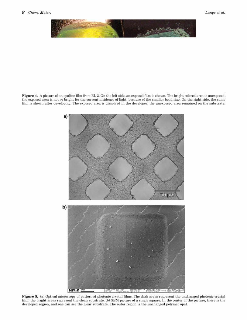
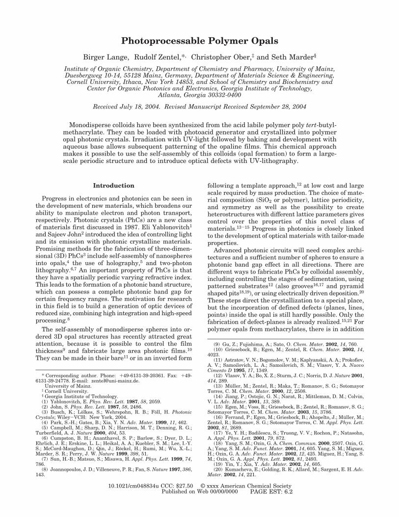
Figure 4. A picture of an opaline film from BL 2. On the left side, an exposed film is shown. The bright colored area is unexposed;the exposed area is not so bright for the current incidence of light, because of the smaller bead size. On the right side, the samefilm is shown after developing. The exposed area is dissolved in the developer; the unexposed area remained on the substrate.
Figure 5. (a) Optical microscopy of patterned photonic crystal films. The dark areas represent the unchanged photonic crystalfilm; the bright areas represent the clean substrate. (b) SEM picture of a single square. In the center of the picture, there is thedeveloped region, and one can see the clear substrate. The outer region is the unchanged polymer opal.
F Chem. Mater. Lange et al.

500 W Hg) using a filter (280-400 nm). Time (0.5-10 min)and distances (5-20 cm) were varied.
Development Method. After exposure, the films wereheated at 120 °C for 10 min. The films were then developedin an aqueous sodium carbonate solution (10 wt %) for 30 s,cleaned with distilled water, and dried.
Used Chemicals. The lattices and the cross-link agent weresynthesized using commercially available chemicals withoutfurther purification: Ethylenglycolbismethacrylate (EGBMA)[Acros], tert-butyl-methacrylate (tBMA) [Acros], potassiumpersulfate [Fluka], methacryloyl choride [Acros], methylmag-nesium bromide [Aldrich], butyrolactone [Fluka], and PAG(CAS 307531-76-6) [Aldrich].
The dye was made at Arizona University in the group of S.Marder; the synthesis is to be published.
Acknowledgment. Financial support by the DFG(Priority program: Photonic crystals) is gratefully ac-knowledged. Additional support from the National Sci-ence Foundation NIRT and STC program is also ac-knowledged. We thank G. Glaser from the MPI forPolymer Research in Mainz for SEM measurements.
CM048834U
Photoprocessable Polymer Opals PAGE EST: 6.2 Chem. Mater. G