Embed Size (px)
Citation preview

, .
.
I.
P
A
Fourth Quarterly Report
for
PHOTON-COUPLED I SOLAT ION SWITCH
( 1 October to 31 December 1966)
Contract No. 951340
Prepared by
E. L. Bonin
of
Texas Instruments Incorporated Semiconductor- Components Division
Post Office Box 5012 Dallas 22, Texas
for
Jet Propulsion Laboratory California Institute of Technology
4800 Oak Grove Drive Pasadena, California 91103
https://ntrs.nasa.gov/search.jsp?R=19670018320 2019-03-15T12:28:00+00:00Z
This work was performed for the Jet hpbialr Lahatmy, California Institute of Technology, sponsored by the National Aeronautics and Space Administration under Contra AS7-100.- 25% ?
d u a r t e r l y Report 3 ,
”/‘?
// 5 PHOTON-COUPLED I SOLAT ION SWITCH y 1 October t q l December 1966) 6 ~ ~ c - ~ b
Contract No.651340 - 2qfi
Prepared by
E. L. Bonin 9
of
allas 22, Texas
for
Jet Propulsion Laboratory California Institute of Technology
4800 Oak Grove Drive Pasadena, California 91103

Report No. 03-67-39
ABSTRACT
A new type of integrated circuit switch is being developed. This device, called the Photon Coupled Isolation Switch, uses internal photon generation and detection techniques to provide electrical isolation between the driving sources and all other terminals of the switch. The Isolation Switch combines a monolithic silicon (Si) inte- grated circuit, a gallium arsenide (GaAs) photon emitting diode, and a silicon photo- transistor in a single integrated circuit flat package. The integrated circuit delivers bias to the photon emitting diode and, with DTL circuitry, provides for up to 1 0 inputs. The emitting diode is optically coupled to the electrically-isolated phototransistor which provides the output switch terminals.
The development program is divided into two phases:
Phase I, design and breadboarding of the driver circuit and development of the GaAs emitting diode-Si phototransistor pair.
Phase II, integration of the driver circuit and prototype production of the complete isolation switch.
Previously, under Phase I, the design and breadboard evaluation of the driver circuit were substantially completed. The Si phototransistor was also designed and developed. With suitable modification, the transistor demonstrated the desired cur- rent gain, breakdown voltage, and low leakage current. The modification eliminated inversion layer formation on the transistor surface which was found to develop at high temperatures after the GaAs emitting diode was bonded to the transistor with an optical coupling glass.
During the fourth quarter, work included additional evaluation of the phototran- sistor leakage and measurements of thermal resistance and noise transmissibility of the emitting diode-phototransistor pair. Coupled pair devices a re also being fabri- cated for delivery under Phase I. Under investigation a re modifications of the driver circuit which will allow use of improved, lower-forward-voltage-drop GaAs emitting diodes and provide lower photon generated leakage in the phototransistor for the off-condition.
iii

.
Report No. 03-67-39
TABLE OF CONTENTS
SECTION
I . II .
III . lv .
TITLE
INTRODUCTION . . . . . . . . TECHNICAL DISCUSSION . . . . . A . Phototransis tor Leakage Evaluation
B . GaAs Switch . . . . . . . 1 . Device Fabrication . . . . 2 . Thermal Character is t ics . . 3 . Current Gain Character is t ics . 4 . Noise Transmissibil i ty . .
C . Driver Circuit . . . . . . . CONCLUSIONS AND RECOMMENDATIONS
REFERENCES . . . . . . . .
. . . . . .
. . . . . . .
. . . . . .
. . . . . .
. . . . . .
. . . . . .
. . . . . .
. . . . . .
. . . . . .
. . . . . .
. . . . . .
PAGE
1
3
3
3
3
4
6
8
10
13
14
iv

Report No. 03-67-39
SECTION I
INTRODUCTION
Electrical isolation, such as obtained using a transformer, offers the highly desirable capability to couple signals between circuits operating at different dc poten- tials and to minimize ground-loop currents produced with direct connections. This four-terminal network operation is not available in most integrated circuits, however, because it cannot be provided effectively with conventional processing techniques. A technique which has successfully provided isolation consists of using photon coupling between a solid state photon emitter-detector pair. The most efficient signal coupling between an optical pair has been obtained using a gallium arsenide (GaAs) P-N junction emitting diode with a silicon (Si) P-N junction diode, both of which have responses which peak near 0 .9 pm at 25' C. The process technologies for these semi- conductor materials a r e also highly advanced. Devices which have been developed%!/ using photon coupling include an isolated input transistor, an isolated-gate P-N-P-N type switch, a multiplex switch requiring no driving transistor, and an isolated-input pulse amplifier.
In the present contract, photon coupling is used in a new type of device consist- ing of a DTL gate having isolated switch output terminals. This three-chip isolation switch combines a monolithic Si driver circuit, a GaAs emitting diode, and a Si photo- transistor. Inputs (up to 10) a r e applied to the driver circuit which supplies forward bias to the GaAs diode. The emitting diode is optically coupled to the phototransistor using a high-refractive index glass. The output transistor is thereby electrically isolated from the driving sources. This development program is divided into two phases. In Phase I, the emitting diode-phototransistor pair (GaAs Switch) is developed and the driver circuit is designed and breadboarded. In Phase 11, the driver circuit is integrated in a monolithic Si wafer and the complete Isolation Switch is assembled in a miniature integrated circuit flat package.
In the first three quarters of the program under Phase I, the phototransistor was successfully developed and the design of the driver circuit substantially completed. In an initial design of the phototransistor, it was found that inversion layers could form over the surfaces of either the collector o r base areas at some temperatures and bias currents after the GaAs emitting diode was bonded to the transistor with a coupling glass. These inversion layers resulted in excessive leakage currents. Modifications of the t ransis tor i l , which included the addition of a guard-ring around the collector- base junction and an increase in the base impurity doping concentration, eliminated
1

Report No. 03-67-39
the effects of inversion layers. GaAs Switches, which combine the phototransistor with a photon emitting diode, demonstrated the design requirements for overall cur- rent gain, breakdown voltage and leakage characteristics. Design criteria for inte- grating the driver circuit were obtained through measurement of numerous elements on integrated circuit wafers used in another optically-coupled device, the Optoelec- tronic Pulse Amplifier (OPA), Texas Instruments type SNX1304. The integrated driver will be made with processing identical to that used for the integrated circuit wafer in the OPA. Also, the GaAs diode in the Isolation Switch will be identical to that in the OPA. With this design information, the driver circuit was designed and breadboarded. Performance tests on the breadboard indicated the circuit would meet design specifications.
In the fourth quarter, studies of the phototransistor leakage current and GaAs Switch overall current gain were completed. Measurements w e r e made of the tem- perature rise of the GaAs wafer under worst case biasing conditions and of the noise transmissibility of the GaAs Switch, using the new phototransistor design. Construc- tion of GaAs Switches for delivery under Phase I was begun. Developments, in a project outside this contract effort, also resulted in a reduction in the forward voltage drop of GaAs diodes. Because the design limits used in the driver circuit design would exclude the use of some of these improved devices, a study of changes in the driver which would allow use of the lower forward drop diodes was begun. The study included possible changes in the driver circuit further reducing the photon generated leakage in the phototransistor in the off-condition.
2
Report No. 03-67-39
SECTION I1
TECHNICAL DISCUSSION
A. PHOTOTRANSISTOR LEAKAGE EVALUATION
Distributions of the collector-emitter leakage currents, IC 0, at 20 V and 100°C for transistors from several slices were previously presented. 3 7 During this period, the leakage currents for transistors from several additional slices were measured. The range of the leakage currents was similar to previous results. The collector- base leakage currents, ICB, are in close agreement with the state-of-the-art range of 1 to 50 nA at 100OC. Previous r e s u l t s / indicated that, for an ICB of 50 nA, the corresponding ICEO is about 20 PA at 100" C (a gain of 400). A value for ICEO of 20 pA at 100" C is also the maximum specified value for the GaAs Switch. Although the yield is affected, a tentative maximum value for ICEO of 10 pA at 20 V and 100" C will be used a s the initial specification to allow for ageing effects which might increase leak- age by as much as a factor of 2.
B. GaAsSWITCH
1. Device Fabrication
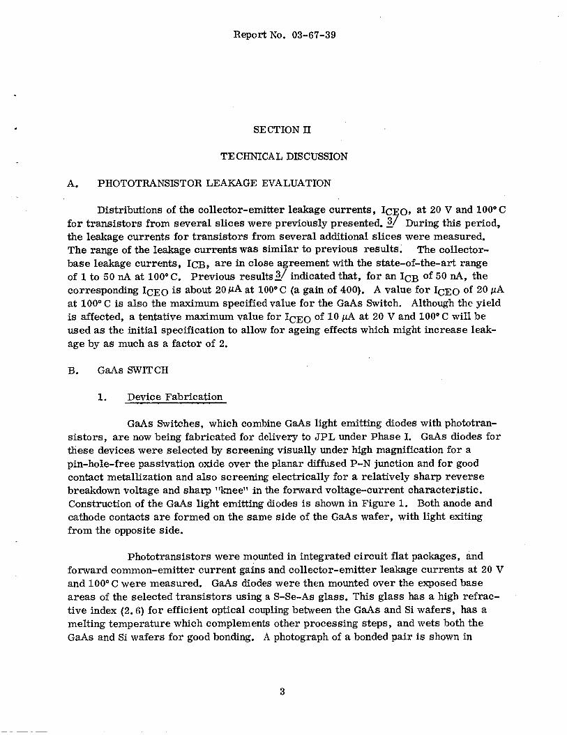
GaAs Switches, which combine GaAs light emitting diodes with phototran- sistors, a re now being fabricated for delivery to JPL under Phase I. GaAs diodes for these devices w e r e selected by screening visually under high magnification for a pin-hole-free passivation oxide over the planar diffused P-N junction and for good contact metallization and also screening electrically for a relatively sharp reverse breakdown voltage and sharp in the forward voltage-current characteristic. Construction of the GaAs light emitting diodes is shown in Figure 1. Both anode and cathode contacts a r e formed on the same side of the GaAs wafer, with light exiting from the opposite side.
Phototransistors were mounted in integrated circuit flat packages, and forward common-emitter current gaks and collector-emitter leakage currents at 20 V and 100" C were measured. GaAs diodes were then mounted over the exposed base areas of the selected transistors using a S-Se-As glass. This glass has a high refrac- tive index (2 .6) for efficient optical coupling between the GaAs and Si wafers, has a melting temperature which complements other processing steps, and wets both the GaAs and Si wafers for good bonding. A photograph of a bonded pair is shown in
3
Report No. 03-67-39
N-TYPE
S C Q 8 2 . 5 9
M E T A L CONTACTS 7 A- P-TYPE
OXIDE\ \ / I
P - N
PHOTON E X I T S U R F A C E JUNCTION
Figure 1. GaAs Photon Emitting Diode
Figure 2. After inspection of the devices, an encapsulation epoxy w a s applied to half the devices, as devices will be shipped both with and without epoxy. Each device has been inserted in a test set which applies 50 mA forward bias to the GaAs diodes in a 25" C ambient. The devices are to be removed after a 100 hour period. Following this burn-in, the devices will be canned and given final testing.
2. Thermal Characteristics
The construction of the GaAs Switch is indicated in the cross-section drawing in Figure 3. It can be seen that the thermal path for heat dissipated in the GaAs diode is through the coupling glass, the transistor, and the package base materi- al to the heat sink. The thermal resistance between the GaAs diode and heat sink w e r e
4

Report No. 03-67-39
5C08260
Figure 2. Si Phototransistor and GaAs Switch
measured for three devices. The measuring technique consisted of using the voltage drop of the GaAs diode at a forward current of 5 mA as the temperature indicating parameter. The voltage drop at 5 m A was first measured over the temperature range of 25" C to 100" C. The measured characteristics are shown in Figure 4. Because there is little temperature r i se at 5 mA bias level, these calibration curves provide an accurate measure of the junction temperature of the GaAs wafers . integrated circuit flat-packages were then mounted in pressure contact with a 25" C heat sink, and power was applied to the GaAs diodes. power w a s interrupted for application of 5 mA and the corresponding forward drop w a s measured with an oscilloscope. The GaAs wafer temperature was then determined using the curves in Figure 4. The thermal resistance was calculated by dividing the rise in the GaAs wafer temperature above that of the heat sink by the average power dissipation. devices. The overall accuracy of the measurements was about 20%. For maximum GaAs diode biasing for the Isolation Switch of 44 mA at 1.46 V at -20" C and 34 mA at 1.25 V at 100" C, as given by worst case analyses, the maximum dissipations a r e 64 mW at -20" C and 42 mW at 100" C. measured of 400" C/W, the indicated maximum temperature rise for the GaAs diode above that of the heat sink at -20" C and 100" C are only about 25" C and 1 7 * C t respec- tively.
The GaAs Switch
For short periods of time, the
The measured thermal resistances were 310,390, and 400" C/W for three
For the largest value of thermal resistance
5

Report No. 03-67-39
L Si PHOTOTRANS ISTOR L G f I A S DIODE
GaAs DIODE
COUPLING GLASS
N EPITAXY COLLECTOR
N+ SUBSTRATE BASE - PACKAGE BASE
HEAT SINK
SECTION A-A
Figure 3. GaAs Switch Construction
3. Current Gain Characteristics
Discussed previously?/ was the relation between the GaAs diode forward bias current and the phototransistor collector current. The collector current is specified to be a minimum of 10 mA at 0 . 6 V collector to emitter voltage and 100" C for the worst-case biasing (of 22 mA) into the GaAs diode. This is a saturated bias- ing condition fo r the transistor. Using a conservative increase of 20% in the equiva- lent base current as sufficient for the out-of saturation condition for GaAs Switches having the least overall current gain, the minimum collector current out-of-saturation at 100°C is 1 2 mA. Allowing an additional 20% factor for both ageing effects in the GaAs diode which might reduce its light emission and in the Si transistor which might

Report No. 03-67-39
- I F - 5 mA
1 .10
1 .0 5
h
3 1.0
W
2 J
0 > 0
0.95 2 :
0.90
0.85
0 CALIBRATION TEMPERATURE ( C )
S C 0 0 2 6 2
Figure 4. GaAs Diode Forward Voltage-Temperature Characteristic
decrease its current gain, the minimum acceptable initial collector current out-of- saturation at 100°C is:
12.0 mA 0. 80 2 = 15 mA
Unsat. IC
Initial 100" c
Of the 18 devices used in Figure 2 of the third quarterly report.?/, which describes the collector currents for worst case biasing, 13 had collector currents of over 15 mA at 100" C out-of-saturation for worst case biasing. Four of the other devices were built
.7

Report No. 03-67-39
with especially low gains (200 < hFE 400) to provide additional points for the low current portion of the figure. Thus the 1g mA minimum value is a quite acceptable value for the GaAs Switch.
4. Noise Transmissibility
The noise transmissibility of the GaAs Switch is defined by the amplitude of the transient signal at the collector of the transistor for 5 V ulses applied at the emitter terminal. A s discussed in the first quarterly report5-T noise transmissibility is related to the P-N junction capacitances of the transistor and the capacitances of the circuit components and measuring jig. The schematic of the measuring jig built to facilitate the integrated circuit flat packages, is shown in Figure 5. Included in the figure are the component, oscilloscope (CRO), and jig capacitances, as determined from direct capacitance measurements and transmissibility measurements using known capacitances in place of the phototransistor.
Noise transmissibility data for several GaAs Switches, using the improved phototransistor design, a r e given in Table I for both positive and negative pulses ap- plied to the emitter terminal. Differences with positive and negative biasing of about 5% are due to the effect of the net collector to emitter voltage on the collector-base capacitance. A value of about 1 . 7 V was obtained, compared with the specified maxi- mum value of 2 V. A value of about 1 . 5 V was previously obtainedL1 for the original design of the transistor. The increase is due to the larger collector-base junction capacitance for the improved structure, due to a 9% increase in the base area and an increase in the base impurity doping concentration. To compensate for these effects, the emitter area for the improved design was reduced by 20%, reducing thebase-emitter junction capacitance at the expense of a slightly greater collector-emitter saturation voltage. These design changes were made to eliminate inversion layer effects, as dis- cussed in the second quarterly report. 6/ -
Several other considerations were made in the measurements. The total jig and oscilloscope capacitances shownin Figure 5 to connect the collector to ac ground (which includes the 0 . 3 pf load resistor capacitance) of 1 0 . 7 pF exceeds the specified minimum capacitance of 10 pF. Also, the 1 . 8 pF capacitance shunting the collector-emitter terminals tends to increase the noise transmissibility slightly. Be- cause of the complex nature of the parasitic capacitances, no correction was made for this shunt capacitance in the data. Thus the data is somewhat conservative. Compli- cating a correction for the shunt capacitance is the capacitance between the GaAs light emitting diode and the phototransistor. Nominally about 3 pF, this capacitance rep- resents the total coupling to the collector and base areas. Values to each of these areas cannot be separated easily. Because the GaAs diode is grounded in the mea- surement, both capacitances a re shunted to ground, This grounded connection of the GaAs diode simulates the connection of the diode in the driver circuit.
8

Report No. 03-67-39
+20 v
?
25n o&L
1 , : r f = i o n s S C 0 5 8 2 2
Figure 5. Noise Transmissibility Jig with Parasitic Capacitances
Table I. Noise Transmissibility of GaAs Switch fo r Indicated Pulse Polarity
Device No.
19
21
23
30
33
1.78
1.77
1.70
1.79
1.78
1.69
1 .68
1.60
1.70
1.69
9
Report No. 03-67-39
Another, less-important consideration is the effect of the rise time of the input pulse on the measured transient signal at the collector. The time constant of the circuit, composed of the 1 0 KQ load resistor and the capacitances, is not insignificant compared to the rise time of the input pulse, specified to be 10 ns o r less. For this reason, highly reproducible results requires the use of a single pulse rise time. Re- producibility between two different types of high speed pulse generators may not be better than lo%, with greater transient values being measured with the generator hav- ing the fastest rise time. An input pulse having a 10 ns rise time was used for the values described.
C. DRIVER CIRCUIT
Recent improvements have been made in the metal contacts of the GaAs diode. These improvements have resulted in a significant fraction of recently fabricated diodes which have lower forward voltage drops than the minimum values used in the design of the driver circuit. z/ Representative low forward drop characteristics a re compared with those previously described in Figure 6. In order to allow these lower forward drop diodes to be used in the Isolation Switch, the driver circuit is being re-analyzed to expand the tolerable range of the diode voltage drop. This could possibly be implemented without sacrificing other parameter tolerances by forming additional resistors in the driver circuit with base-type diffusions. Although larger areas will probably be required on the integrated circuit wafer, the smaller temperature coeffi- cient of the base-diffused resistor may result in a circuit design having greater toler- ance of parameter values.
Circuit changes which will further reduce photon generated leakage current in the phototransistor for the off-condition are also under study. Either replacement of each input diode with an active transistor or shunting of the GaAs diode with a resistor (see Figure 7) could result in reduced current in the GaAs diode in the off-condition, thereby reducing the GaAs photon generation and the resulting leakage in the photo- transistor.
10

.
~ ~ ~~
Report NO. 03-67-39
100
I- Z W U U 3 u
10
1
RECENT LOW
SERIES
RESISTANCE
RANGE FOR
PREVIOUS DIODES
0 TC ,= 2 5 C
FORWARD VOLTAGE (V)
SC08263
Figure 6. GaAs Diode V-I Characteristics- Comparison of Previous Diodes with Recent Better Diode
11

Report No. 03-67-39
PRESENT DESIGN
WITH ACTIVE
INPUT TRANSISTOR
WITH SHUNT
ON @AS DIODE S C 0 8 2 6 4
Figure 7. Isolation Switch Circuit and Modifications Under Study
12

Report No. 03-67-39
SECTION 111
CONCLUSIONS AND RECOMMENDATIONS
Tests indicate the GaAs Switch as developed will meet all design specifications, which include overall current gain, breakdown voltage, leakage current, and noise transmissibility. Devices for delivery under Phase I a re being fabricated.
An additional study of the driver circuit is being made to allow use of lower for- ward voltage drop GaAs diodes and consider changes which might further reduce photon generated leakage in the phototransistor.
13

Report No. 03-67-39
1.
2.
3.
4.
5.
6.
J. R. Biard
SECTION IV
REFERENCES
nd W. T. Matzen, '?Advanced Function 1 Electronic Block Develop- ment, No. RTD-TDR-63-4203, January 1964.
Texas Instruments Incorporated, Contract No. AF 33(657)-9824, Report
J. R. Biard, et. al., "Optoelectronics as Applied to Functional Electronic Blocks," IEEE Proceedings, V 52, No. 12, pp. 1529-1536, December 1964.
"Integrated Electronic Gating System for Multiplexing Applications, t f IBM, JPL Contract No. 950492, December 15, 1964.
Texas Instruments Incorporated, "Photon-Coupled Isolation Switch, t ( JPL Contract No. 951340, Third Quarterly Report, 1 July to 30 September, 1966.
Texas Instruments Incorporated, "Photon-Coupled Isolation Switch, Contract No. 951340, First Quarterly Report, 1 January to 31 March, 1966.
JPL
Texas Instruments Incorporated, "Photon Coupled Isolation Switch, JPL Contract No. 951340, Second Quarterly Report, 1 April to 30 June, 1966.
14