Embed Size (px)
Citation preview

Flexible fabrication of a patterned red phosphor layer on a YAG:Ce3+ phosphor-in-glass for high-power WLEDs YANG PENG,1,2 YUN MOU,1 XING GUO,3 XUJIA XU,4 HONG LI,4 MINGXIANG CHEN,1,5 AND XIAOBING LUO2,6 1School of Mechanical Science and Engineering, Huazhong University of Science and Technology, Wuhan 430074, China 2State Key Laboratory of Coal Combustion and Thermal Packaging Laboratory, School of Energy and Power Engineering, Huazhong University of Science and Technology, Wuhan 430074, China 3National Engineering Technology Research Center for LED on Si Substrate, Nanchang University, Nanchang 330047, China 4State Key Laboratory of Silicate Materials for Architectures, Wuhan University of Technology, Wuhan 430070, China [email protected] [email protected]
Abstract: We proposed a flexible and mask-less approach to directly fabricate a patterned red phosphor layer on a Y3Al5O12:Ce3+ (YAG:Ce3+) phosphor-in-glass (PiG) for high-power white light-emitting diodes (WLEDs). This approach was realized by ultraviolet (UV) assisted and initiative cooling based water condensing. A low-temperature precursor glass matrix with a high refractive index was synthesized for the YAG:Ce3+ PiG. By controlling the UV pre-curing time, the micro-concaves with adjustable sizes were fabricated on the red phosphor layer embedded with UV-curable polymer. With the pre-curing time of 20 s, 30 s, and 40 s, the average aspect ratio of the micro-concave is 1.03, 0.76, and 0.41, respectively. Consequently, the patterned sample achieves a highest luminous efficacy (LE) of 108.5 lm/W at the current of 350 mA, which is 16.2% higher than the unpatterned sample. The corresponding correlated color temperature (CCT) and color rendering index (CRI) are 4831 K and 80.5, respectively. The results demonstrate that the YAG:Ce3+ PiG coated with the water condensing patterned red phosphor layer is a feasible and effective method to enhance the light extraction and color quality of high-power WLEDs. © 2018 Optical Society of America under the terms of the OSA Open Access Publishing Agreement
OCIS codes: (230.0230) Optical devices; (230.3670) Light-emitting diodes; (160.4670) Optical materials.
References and links 1. A. Zukauskas, M. S. Shur, and R. Caska, Introduction to Solid-State Lighting (Wiley, 2002). 2. E. F. Schubert and J. K. Kim, “Solid-state light sources getting smart,” Science 308(5726), 1274–1278 (2005). 3. X. Luo, R. Hu, S. Liu, and K. Wang, “Heat and fluid flow in high-power LED packaging and applications,”
Prog. Energ. Combust. 56, 1–32 (2016). 4. S. C. Allen and A. J. Steckl, “A nearly ideal phosphor-converted white light-emitting diode,” Appl. Phys. Lett.
92(14), 143309 (2008). 5. Y. Ma, R. Hu, X. Yu, W. Shu, and X. Luo, “A modified bidirectional thermal resistance model for junction and
phosphor temperature estimation in phosphor-converted light-emitting diodes,” Int. J. Heat Mass Transfer 106, 1–6 (2017).
6. J. S. Lee, S. Unithrattil, S. Kim, I. J. Lee, H. Lee, and W. B. Im, “Robust moisture and thermally stable phosphor glass plate for highly unstable sulfide phosphors in high-power white light-emitting diodes,” Opt. Lett. 38(17), 3298–3300 (2013).
7. L.-Y. Chen, J.-K. Chang, W.-C. Cheng, J.-C. Huang, Y.-C. Huang, and W.-H. Cheng, “Chromaticity tailorable glass-based phosphor-converted white light-emitting diodes with high color rendering index,” Opt. Express 23(15), A1024–A1029 (2015).
8. M. Ma, F. W. Mont, X. Yan, J. Cho, E. F. Schubert, G. B. Kim, and C. Sone, “Effects of the refractive index of the encapsulant on the light-extraction efficiency of light-emitting diodes,” Opt. Express 19(S5), A1135–A1140 (2011).
Vol. 8, No. 3 | 1 Mar 2018 | OPTICAL MATERIALS EXPRESS 605
#319022 https://doi.org/10.1364/OME.8.000605 Journal © 2018 Received 3 Jan 2018; revised 5 Feb 2018; accepted 6 Feb 2018; published 12 Feb 2018
9. X. Xu, H. Li, Y. Zhuo, R. Li, P. Tian, D. Xiong, and M. Chen, “High refractive index coating of phosphor-in-glass for enhanced light extraction efficiency of white LEDs,” J. Mater. Sci. 53(2), 1335–1345 (2018).
10. Y. K. Lee, J. S. Lee, J. Heo, W. B. Im, and W. J. Chung, “Phosphor in glasses with Pb-free silicate glass powders as robust color-converting materials for white LED applications,” Opt. Lett. 37(15), 3276–3278 (2012).
11. R. Zhang, H. Lin, Y. Yu, D. Chen, J. Xu, and Y. Wang, “A new-generation color converter for high-power white LED: transparent Ce3+:YAG phosphor-in-glass,” Laser Photonics Rev. 8(1), 158–164 (2014).
12. Y. Peng, S. Wang, R. Li, H. Li, H. Cheng, M. Chen, and S. Liu, “Luminous efficacy enhancement of ultraviolet-excited white light-emitting diodes through multilayered phosphor-in-glass,” Appl. Opt. 55(18), 4933–4938 (2016).
13. Y. Peng, R. Li, H. Cheng, Z. Chen, H. Li, and M. Chen, “Facile preparation of patterned phosphor-in-glass with excellent luminous properties through screen-printing for high-power white light-emitting diodes,” J. Alloys Compd. 693, 279–284 (2017).
14. X. Zhang, J. Yu, J. Wang, B. Lei, Y. Liu, Y. Cho, R.-J. Xie, H.-W. Zhang, Y. Li, Z. Tian, Y. Li, and Q. Su, “All-inorganic light convertor based on phosphor-in-glass engineering for next-generation modular high-brightness white LEDs/LDs,” ACS Photonics 4(4), 986–995 (2017).
15. Y. H. Kim, N. S. M. Viswanath, S. Unithrattil, H. J. Kim, and W. B. Im, “Review—Phosphor plates for high-power LED applications: challenges and opportunities toward perfect lighting,” ECS J. Solid State Sci. Technol. 7(1), R3134–R3147 (2018).
16. L. Yang, M. Chen, Z. Lv, S. Wang, X. Liu, and S. Liu, “Preparation of a YAG:Ce phosphor glass by screen-printing technology and its application in LED packaging,” Opt. Lett. 38(13), 2240–2243 (2013).
17. Y. Peng, R. Li, S. Wang, Z. Chen, L. Nie, and M. Chen, “Luminous properties and thermal reliability of screen-printed phosphor-in-glass-based white light-emitting diodes,” IEEE T. Electron Dev. 64(3), 1114–1119 (2017).
18. Y. K. Lee, Y. H. Kim, J. Heo, W. B. Im, and W. J. Chung, “Control of chromaticity by phosphor in glasses with low temperature sintered silicate glasses for LED applications,” Opt. Lett. 39(14), 4084–4087 (2014).
19. L.-Y. Chen, W.-C. Cheng, C.-C. Tsai, J.-K. Chang, Y.-C. Huang, J.-C. Huang, and W.-H. Cheng, “Novel broadband glass phosphors for high CRI WLEDs,” Opt. Express 22(S3 Suppl 3), A671–A678 (2014).
20. Y. Peng, R. Li, X. Guo, H. Zheng, and M. Chen, “Optical performance improvement of phosphor-in-glass based white light-emitting diodes through optimized packaging structure,” Appl. Opt. 55(29), 8189–8195 (2016).
21. Z. Lin, H. Lin, J. Xu, F. Huang, H. Chen, B. Wang, and Y. Wang, “Highly thermal-stable warm w-LED based on Ce:YAG PiG stacked with a red phosphor layer,” J. Alloys Compd. 649, 661–665 (2015).
22. Y. H. Kim, P. Arunkumar, B. Y. Kim, S. Unithrattil, E. Kim, S.-H. Moon, J. Y. Hyun, K. H. Kim, D. Lee, J.-S. Lee, and W. B. Im, “A zero-thermal-quenching phosphor,” Nat. Mater. 16(5), 543–550 (2017).
23. J. S. Kim, S. K. Eswaran, O. H. Kwon, S. J. Han, J. H. Lee, and Y. S. Cho, “White-light-emitting diodes: enhanced luminescence characteristics of remote yellow silicate phosphors printed on nanoscale surface-roughened glass substrates for white light-emitting diodes,” Adv. Opt. Mater. 4(7), 976 (2016).
24. Y. Peng, X. Guo, R. Li, H. Cheng, and M. Chen, “Thermally stable WLEDs with excellent luminous properties by screen-printing a patterned phosphor glass layer on a microstructured glass plate,” Appl. Opt. 56(12), 3270–3276 (2017).
25. Y.-K. Ee, P. Kumnorkaew, R. A. Arif, H. Tong, J. F. Gilchrist, and N. Tansu, “Light extraction efficiency enhancement of InGaN quantum wells light-emitting diodes with polydimethylsiloxane concave microstructures,” Opt. Express 17(16), 13747–13757 (2009).
26. S. Wang, Y. Li, L. Feng, L. Zhang, Y. Zhang, X. Su, W. Ding, and F. Yun, “Laser patterning of Y3Al5O12:Ce3+ ceramic phosphor platelets for enhanced forward light extraction and angular color uniformity of white LEDs,” Opt. Express 24(15), 17522–17531 (2016).
27. R. Liang, F. Wu, S. Wang, Q. Chen, J. Dai, and C. Chen, “Enhanced optical and thermal performance of eutectic flip-chip ultraviolet light-emitting diodes via AlN-doped-silicone encapsulant,” IEEE T. Electron Dev. 64(2), 467–471 (2017).
28. H.-T. Hsieh and G.-D. J. Su, “A novel boundary-confined method for high numerical aperture microlens array fabrication,” J. Micromech. Microeng. 20(3), 035023 (2010).
29. H. Jung and K.-H. Jeong, “Monolithic polymer microlens arrays with high numerical aperture and high packing density,” ACS Appl. Mater. Interfaces 7(4), 2160–2165 (2015).
30. J. Yong, F. Chen, Q. Yang, G. Du, H. Bian, D. Zhang, J. Si, F. Yun, and X. Hou, “Rapid fabrication of large-area concave microlens arrays on PDMS by a femtosecond laser,” ACS Appl. Mater. Interfaces 5(19), 9382–9385 (2013).
31. B. Bao, J. Jiang, F. Li, P. Zhang, S. Chen, Q. Yang, S. Wang, B. Su, L. Jiang, and Y. Song, “Fabrication of patterned concave microstructures by inkjet imprinting,” Adv. Funct. Mater. 25(22), 3286–3294 (2015).
32. M. Kuang, L. Wang, and Y. Song, “Controllable printing droplets for high-resolution patterns,” Adv. Mater. 26(40), 6950–6958 (2014).
33. Y. Peng, X. Guo, R. Liang, Y. Mou, H. Cheng, M. Chen, and S. Liu, “Fabrication of microlens arrays with controlled curvature by micromolding water condensing based porous films for deep ultraviolet LEDs,” ACS Photonics 4(10), 2479–2485 (2017).
34. X.-H. Li, R. Song, Y.-K. Ee, P. Kumnorkaew, J. F. Gilchrist, and N. Tansu, “Light extraction efficiency and radiation patterns of III-nitride light-emitting diodes with colloidal microlens arrays with various aspect ratios,” IEEE Photonics J. 3(3), 489–499 (2011).
Vol. 8, No. 3 | 1 Mar 2018 | OPTICAL MATERIALS EXPRESS 606

1. Introduction White light-emitting diodes (WLEDs) have been widely applied in display backlighting, street lamps, headlamps, and indoor illuminations due to their compact size, energy saving, environmental friendly, and long lifetime [1–3]. Currently, the commercial phosphor-converted WLEDs can be produced by the combination of blue LED chips and yellow Y3Al5O12:Ce3+ (YAG:Ce3+) phosphor embedded with organic resins [4,5]. However, for high-power WLEDs, the organic encapsulants with poor thermal and photonic stability may age easily and turn yellow during long-time service, resulting in the reduction of luminous efficacy (LE), the shift of chromaticity, and the degradation of long-term reliability [6,7]. In addition, the refractive index of organic encapsulants (~1.5) is lower than that of the YAG:Ce3+ phosphor (~1.83), which reduces the light escaped from phosphor particles due to the reflection loss [8,9].
To overcome the weaknesses of organic encapsulants, phosphor-in-glass (PiG), which is prepared by a low-temperature (<800°C) sintering of glass powders and phosphor particles, has been employed as a promising luminescent converter for high-power WLEDs because of its robust, high thermal stability, and low thermal expansion coefficient [10–15]. Furthermore, the precursor glass matrix can achieve a high refractive index for the PiG converter by adding ions of large polarizability. In the last year, we have innovatively developed YAG:Ce3+ based PiG converter by introducing yellow YAG:Ce3+ phosphor embedded with borosilicate glass through screen-printing and low-temperature sintering, which yields cool white light with a LE of 114 lm/W, a correlated color temperature (CCT) of 5524 K, and a color rendering index (CRI) of 69 [16,17]. Unfortunately, this YAG:Ce3+ PiG is notoriously difficult to achieve natural white light with high CRI due to the deficiency of red spectrum in the emission light. In order to increase the CRI, multi-components PiG is introduced by adding red CaAlSiN3:Eu2+ (CASN:Eu2+) phosphor into the glass matrix [18–20]. It should be noted that the red phosphor prone to thermal degradation during co-sintering and has an interfacial reaction with the glass matrix, both of which reduce the quantum efficiency of red phosphor [21,22]. In addition, the PiG converter with flat surface has total internal reflection (TIR) at the glass-air interface because of the different refractive index between glass and air, which leads to the trapped loss of light in the remote-type LED package [23,24]. It is well known that micro/nano patterned structures can reduce the TIR loss and enhance light extraction [25–27]. Currently, various strategies have been proposed to fabricate the patterned structures, including lithography [28], photoresist reflow [29], direct laser writing [30], and inkjet imprinting [31]. However, most strategies involve at least one photolithographic step, which suffers from some disadvantages of high-cost, time-consuming, and heavy pollution. Although direct laser writing can fabricate the patterned structure with high precision, it is expensive and inefficient for large-area fabrication. The appeal of inkjet printing lies in it being a mask-less, large-scale, and low-cost manufacturing. But this method is limited by inhomogeneous morphology and large feature size [32]. Therefore, it still is a challenge to fabricate the YAG:Ce3+ PiG with high light extraction and color quality by using a flexible and effective method.
Herein, a patterned red phosphor layer was fabricated on a YAG:Ce3+ PiG by using a flexible and mask-less water condensing approach, which not only avoids the thermal and chemical degradation of red phosphor during co-sintering but also enhances light extraction from LED package. A low-temperature glass matrix with a matching refractive index of YAG:Ce3+ phosphor was synthesized. The YAG:Ce3+ PiG was prepared by screen-printing and co-sintering. The micro-concave array was fabricated on the red phosphor layer through ultraviolet (UV) assisted and initiative cooling based water condensing. The aspect ratio of micro-concave was adjusted by controlling UV pre-curing time. The WLED modules were packaged by the YAG:Ce3+ PiGs with the patterned red phosphor layers and their optical performances were investigated.
Vol. 8, No. 3 | 1 Mar 2018 | OPTICAL MATERIALS EXPRESS 607
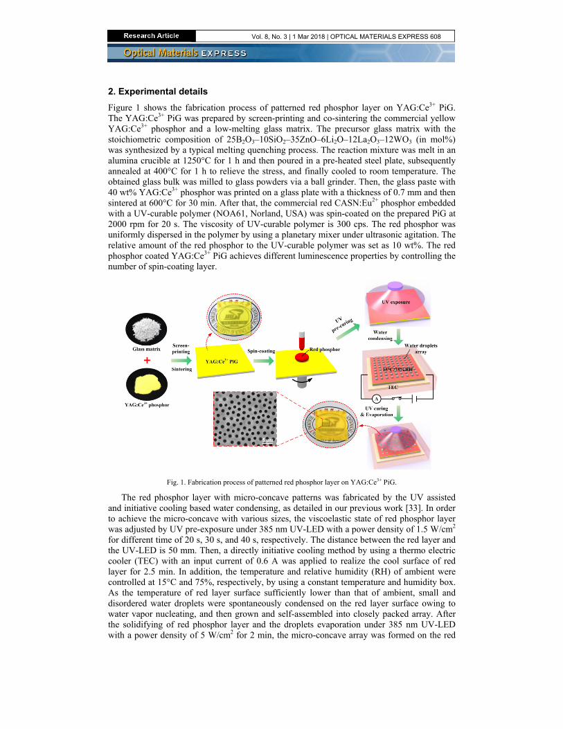
2. Experimental details Figure 1 shows the fabrication process of patterned red phosphor layer on YAG:Ce3+ PiG. The YAG:Ce3+ PiG was prepared by screen-printing and co-sintering the commercial yellow YAG:Ce3+ phosphor and a low-melting glass matrix. The precursor glass matrix with the stoichiometric composition of 25B2O3–10SiO2–35ZnO–6Li2O–12La2O3–12WO3 (in mol%) was synthesized by a typical melting quenching process. The reaction mixture was melt in an alumina crucible at 1250°C for 1 h and then poured in a pre-heated steel plate, subsequently annealed at 400°C for 1 h to relieve the stress, and finally cooled to room temperature. The obtained glass bulk was milled to glass powders via a ball grinder. Then, the glass paste with 40 wt% YAG:Ce3+ phosphor was printed on a glass plate with a thickness of 0.7 mm and then sintered at 600°C for 30 min. After that, the commercial red CASN:Eu2+ phosphor embedded with a UV-curable polymer (NOA61, Norland, USA) was spin-coated on the prepared PiG at 2000 rpm for 20 s. The viscosity of UV-curable polymer is 300 cps. The red phosphor was uniformly dispersed in the polymer by using a planetary mixer under ultrasonic agitation. The relative amount of the red phosphor to the UV-curable polymer was set as 10 wt%. The red phosphor coated YAG:Ce3+ PiG achieves different luminescence properties by controlling the number of spin-coating layer.
Fig. 1. Fabrication process of patterned red phosphor layer on YAG:Ce3+ PiG.
The red phosphor layer with micro-concave patterns was fabricated by the UV assisted and initiative cooling based water condensing, as detailed in our previous work [33]. In order to achieve the micro-concave with various sizes, the viscoelastic state of red phosphor layer was adjusted by UV pre-exposure under 385 nm UV-LED with a power density of 1.5 W/cm2 for different time of 20 s, 30 s, and 40 s, respectively. The distance between the red layer and the UV-LED is 50 mm. Then, a directly initiative cooling method by using a thermo electric cooler (TEC) with an input current of 0.6 A was applied to realize the cool surface of red layer for 2.5 min. In addition, the temperature and relative humidity (RH) of ambient were controlled at 15°C and 75%, respectively, by using a constant temperature and humidity box. As the temperature of red layer surface sufficiently lower than that of ambient, small and disordered water droplets were spontaneously condensed on the red layer surface owing to water vapor nucleating, and then grown and self-assembled into closely packed array. After the solidifying of red phosphor layer and the droplets evaporation under 385 nm UV-LED with a power density of 5 W/cm2 for 2 min, the micro-concave array was formed on the red
Vol. 8, No. 3 | 1 Mar 2018 | OPTICAL MATERIALS EXPRESS 608

phosphor layer by treating water droplets array as templates. Finally, the micro-concave patterns with different aspect ratios were fabricated by controlling the UV pre-curing time.
For the packaging of high-power WLEDs, four blue LED chips (2 × 2) with a peak wavelength of 454 nm were attached and wire bonded at the bottom of substrate. The fabricated color converters were bonded on the top of substrate and the patterned red phosphor layer faced outward. The gap between the chips and the converters was filled with silicone encapsulant, which can reduce the reflection loss at the chip surface and enhance light extraction. The glass transition temperature (Tg) and the crystallization temperature (Tc) of the prepared glass matrix were analyzed by simultaneous thermal analysis (STA449F3, Netzsch, Germany). The refractive index of the prepared glass matrix was measured by spectroscopic ellipsometry (M-2000V, J. A. Woollam, USA). The photoluminescence excitation (PLE) and PL emission spectra of the YAG:Ce3+ PiG and the red phosphor coated PiGs were recorded on a fluorescence spectrophotometer (FP-6500, Jasco, Japan). The YAG:Ce3+ PiG and the micro-concave patterns were characterized by using a scanning electron microscope (SEM, Nova NanoSEM 450, FEI) equipped with an energy dispersive spectrometer (EDS). The electroluminescence (EL) spectra, LE, CCT, CRI, and chromaticity coordinate of WLED modules were measured in an integrating sphere (HAAS-2000, Everfine, China) with a diameter of 50 cm. The far-field emission intensity of WLED modules was measured by a light intensity distribution (LID) curve tester (GO1900L, Everfine, China).
3. Results and discussion Figure 2(a) presents the differential scanning calorimetry (DSC) thermal analysis of the prepared glass matrix. In the DSC curve, the glass transition temperature (Tg) can be found at 520°C and the crystallization temperature (Tc) is estimated to be 635°C. This result indicates that the prepared glass matrix achieves low melting temperature without crystallization in the temperature interval of 520-635°C. The refractive index of prepared glass matrix was measured, as shown in Fig. 2(b). It is shown that the glass matrix yields a similar refractive index (~1.82 at 460 nm) with the YAG:Ce3+ phosphor, which can reduce the reflection loss at the phosphor particles.
Fig. 2. (a) DSC curve and (b) measured refractive index of prepared glass matrix.
The PLE and PL spectra of the prepared YAG:Ce3+ PiG is shown in Fig. 3(a). The PLE spectrum of the YAG:Ce3+ PiG displays two excitation bands centered at 342 nm and 463 nm originating from the 4f→5d transition of Ce3+. The PL spectrum of the YAG:Ce3+ PiG exhibits a typical Ce3+:5d→4f broadband emission centered at 541 nm under 463 nm excitation. Figure 3(b) presents the PL emission spectra of the YAG:Ce3+ PiG coated with the different number of red phosphor layers. As the increase of red layer, the yellow emission
Vol. 8, No. 3 | 1 Mar 2018 | OPTICAL MATERIALS EXPRESS 609

intensity decreases while the red emission intensity increases, and the peak wavelength changes from 541 nm to 583 nm, which can improve the light quality.
Fig. 3. (a) Normalized PLE and PL spectra of prepared YAG:Ce3+ PiG. (b) PL emission spectra of prepared YAG:Ce3+ PiG coated with different number of red phosphor layers.
Figure 4(a) and (b) show the photographs of the unpatterned and patterned samples with different red phosphor layers coated on YAG:Ce3+ PiG, respectively. With the increasing number of layers of red phosphor layer, the transparency of samples is reduced because a larger fraction of the emitted light is scattered. The patterned samples exhibit less transparency compared with the unpatterned samples due to the scattering properties of micro-concave structure. The cross-sectional image of the patterned sample with 3-red layer is shown in Fig. 4(c). The thickness of YAG:Ce3+ glass layer and red phosphor layer is 40 μm and 35 μm, respectively. Obviously, the micro-concave array is formed on the red phosphor layer. It is difficult to discover some agglomerates and any interfacial phase between the YAG:Ce3+ phosphors and the glass matrix, and the Y, Al, and O signals were detected on the YAG:Ce3+ phosphor. This result demonstrates that the YAG:Ce3+ microcrystals are well embedded in the glass matrix to form the YAG:Ce3+ PiG.
Vol. 8, No. 3 | 1 Mar 2018 | OPTICAL MATERIALS EXPRESS 610

Fig. 4. Photographs of (a) unpatterned samples and (b) patterned samples with different red phosphor layers. (c) Cross-sectional SEM image of patterned sample and EDS curve of YAG:Ce3+ glass layer.
The micro-concave arrays were fabricated on the red phosphor layers by the water condensing method. The YAG:Ce3+ PiG coated with the 3-red phosphor layer were used for the fabrication of the micro-concave arrays. Figure 5(a)-(c) show the top and cross-sectional SEM images of the fabricated micro-concave arrays at the different UV pre-curing time. With the UV pre-curing time of 20 s, the relatively uniform concave array with the average width of 1.47 μm and the average depth of 1.51 μm is achieved on the surface of red phosphor layer. As the UV pre-curing time increases, the average width increases and the average depth decreases, and the distribution of micro-concave array becomes nonuniform at the UV pre-curing time of 40 s. With the UV pre-curing time of 20 s, 30 s, and 40 s, the average aspect ratio of micro-concave is 1.03, 0.76, and 0.41, respectively. It is attributed to the fact that the red layer surface changes from a viscous liquid to a viscoelastic state when the UV pre-curing time increases, which reduces the penetrating depth of water droplets on the surface and increases the probability of water droplets coalesce. Thus, a conclusion can be drawn that the micro-concave arrays with different aspect ratios can be easily fabricated on the red phosphor layer by using the time-saving and low-cost water condensing method.
Vol. 8, No. 3 | 1 Mar 2018 | OPTICAL MATERIALS EXPRESS 611
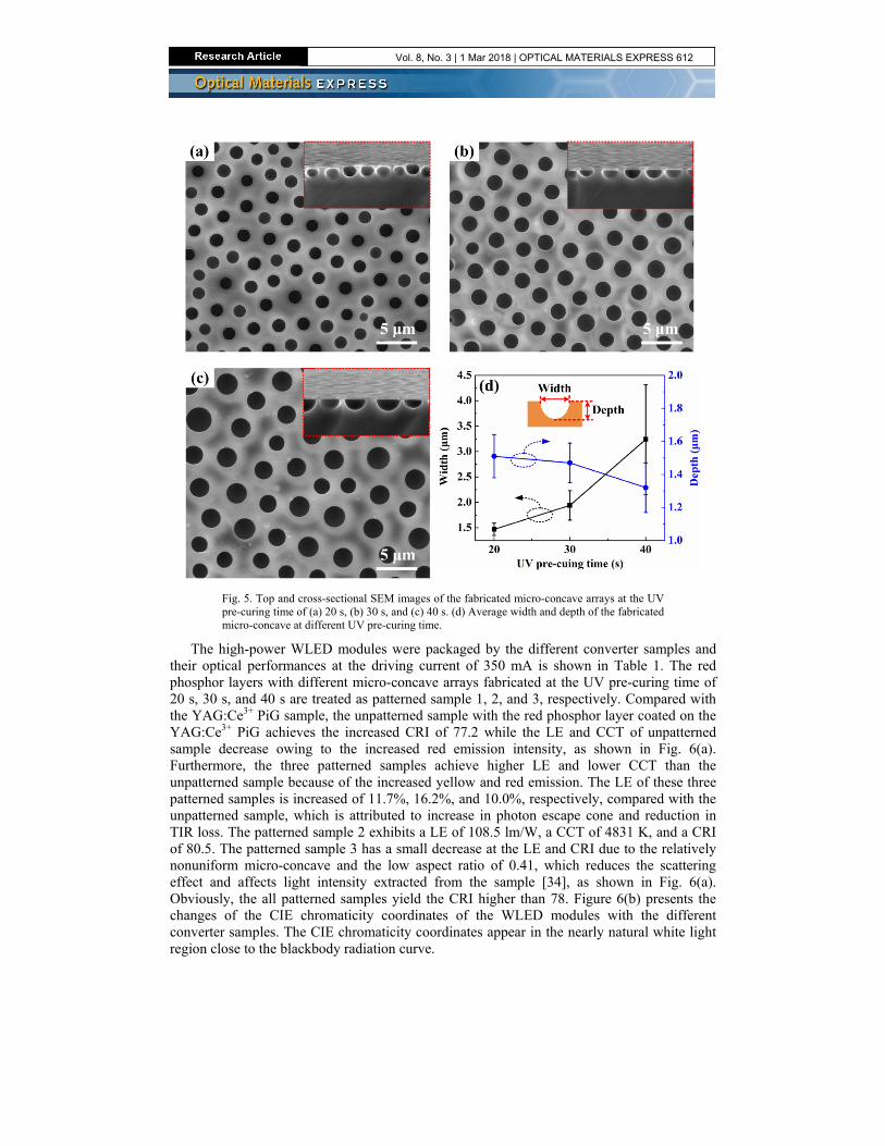
Fig. 5. Top and cross-sectional SEM images of the fabricated micro-concave arrays at the UV pre-curing time of (a) 20 s, (b) 30 s, and (c) 40 s. (d) Average width and depth of the fabricated micro-concave at different UV pre-curing time.
The high-power WLED modules were packaged by the different converter samples and their optical performances at the driving current of 350 mA is shown in Table 1. The red phosphor layers with different micro-concave arrays fabricated at the UV pre-curing time of 20 s, 30 s, and 40 s are treated as patterned sample 1, 2, and 3, respectively. Compared with the YAG:Ce3+ PiG sample, the unpatterned sample with the red phosphor layer coated on the YAG:Ce3+ PiG achieves the increased CRI of 77.2 while the LE and CCT of unpatterned sample decrease owing to the increased red emission intensity, as shown in Fig. 6(a). Furthermore, the three patterned samples achieve higher LE and lower CCT than the unpatterned sample because of the increased yellow and red emission. The LE of these three patterned samples is increased of 11.7%, 16.2%, and 10.0%, respectively, compared with the unpatterned sample, which is attributed to increase in photon escape cone and reduction in TIR loss. The patterned sample 2 exhibits a LE of 108.5 lm/W, a CCT of 4831 K, and a CRI of 80.5. The patterned sample 3 has a small decrease at the LE and CRI due to the relatively nonuniform micro-concave and the low aspect ratio of 0.41, which reduces the scattering effect and affects light intensity extracted from the sample [34], as shown in Fig. 6(a). Obviously, the all patterned samples yield the CRI higher than 78. Figure 6(b) presents the changes of the CIE chromaticity coordinates of the WLED modules with the different converter samples. The CIE chromaticity coordinates appear in the nearly natural white light region close to the blackbody radiation curve.
Vol. 8, No. 3 | 1 Mar 2018 | OPTICAL MATERIALS EXPRESS 612
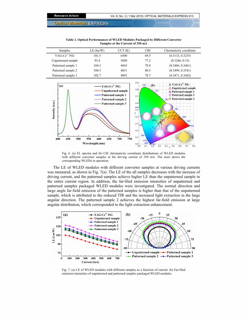
Table 1. Optical Performances of WLED Modules Packaged by Different Converter Samples at the Current of 350 mA
Samples LE (lm/W) CCT (K) CRI Chromaticity coordinate
YAG:Ce3+ PiG 101.5 6500 69.5 (0.3133, 0.3255)
Unpatterned sample 93.4 5680 77.2 (0.3286, 0.33)
Patterned sample 1 104.3 4843 78.9 (0.3486, 0.3461)
Patterned sample 2 108.5 4831 80.5 (0.3499, 0.3541)
Patterned sample 3 102.7 4893 78.7 (0.3471, 0.3442)
Fig. 6. (a) EL spectra and (b) CIE chromaticity coordinate distributions of WLED modules with different converter samples at the driving current of 350 mA. The inset shows the corresponding WLEDs in operation.
The LE of WLED modules with different converter samples at various driving currents was measured, as shown in Fig. 7(a). The LE of the all samples decreases with the increase of driving current, and the patterned samples achieve higher LE than the unpatterned sample in the entire current region. In addition, the far-filed emission intensities of unpatterned and patterned samples packaged WLED modules were investigated. The normal direction and large angle far-field emission of the patterned samples is higher than that of the unpatterned sample, which is attributed to the reduced TIR and the increased light extraction in the large angular direction. The patterned sample 2 achieves the highest far-field emission at large angular distribution, which corresponded to the light extraction enhancement.
Fig. 7. (a) LE of WLED modules with different samples as a function of current. (b) Far-filed emission intensities of unpatterned and patterned samples packaged WLED modules.
Vol. 8, No. 3 | 1 Mar 2018 | OPTICAL MATERIALS EXPRESS 613
4. Conclusions In this work, a patterned red phosphor layer coated on a YAG:Ce3+ PiG was proposed for high-power WLEDs. The micro-concave patterns were fabricated by using a mask-less, time-saving, and low-cost method of UV assisted and initiative cooling based water condensing. The low-temperature glass matrix with a high refractive index (~1.82) was synthesized for the fabrication of YAG:Ce3+ PiG. With the increase of red layer, the yellow emission intensity of YAG:Ce3+ PiG decreases while the red emission intensity increases. Furthermore, the aspect ratio of micro-concave was adjusted by controlling the UV pre-curing time. As the UV pre-curing time of 20 s, 30 s, and 40 s, the average aspect ratio of micro-concave is 1.03, 0.76, and 0.41, respectively. The LE of these three patterned samples is increased of 11.7%, 16.2%, and 10.0%, respectively, compared with the unpatterned sample at the driving current of 350 mA. This study provides a flexible and effective method for the light extraction and color quality enhancement of high-power WLEDs.
Funding National Natural Science Foundation of China (51775219 and 51705230); National Key Research and Development Program of China (2016YFB0400804); Fundamental Research Funds for the Central Universities (2016JCTD112).
Acknowledgements The authors would like to thank Analytical and Testing Center of Huazhong University of Science and Technology for the support in DSC, PL, and SEM measurement.
Vol. 8, No. 3 | 1 Mar 2018 | OPTICAL MATERIALS EXPRESS 614