Embed Size (px)
Citation preview
IEEE TRANSACTIONS ON POWER ELECTRONICS, VOL. 28, NO. 1, JANUARY 2013 199
Perturbation On-Time (POT) Technique in PowerFactor Correction (PFC) Controller for Low Total
Harmonic Distortion and High Power FactorJen-Chieh Tsai, Chi-Lin Chen, Yi-Ting Chen, Chia-Lung Ni, Chun-Yen Chen,
and Ke-Horng Chen, Senior Member, IEEE
Abstract—The proposed perturbation on-time technique sup-presses total harmonic distortion (THD) and, thus, improves thepower factor in the power factor correction (PFC) controller. Be-sides, the adaptive control of the minimum off time by the proposedinhibit time control can improve efficiency even at low ac input volt-age. Therefore, highly integrated PFC converter fabricated in theTSMC 800-V ultrahigh voltage process can achieve low THD of6%, high PF of 99%, and high efficiency of 95% at the outputpower of 90 W.
Index Terms—Inhibit time (IT) control, nonnegative-voltagezero current detector (NNV-ZCD), perturbation on time (POT),power factor correction (PFC), ultrahigh voltage (UHV).
I. INTRODUCTION
THE input line current is basically shaped by the power fac-tor correction (PFC) controller to be the replica of the input
line voltage and exactly in phase with it. If the value of the powerfactor (PF) is not 100%, it results in power losses, harmonicsthat travel down the neutral line, and disruption of other devicesconnected to the line. Therefore, today’s electrical equipmentmust comply with the European Norm EN61000−3−2, whichapplies to most electrical appliances with an input power of 80 Wor greater. Conventional passive PFC techniques with large ex-ternal inductors and capacitors only achieve a PF of about 75%.This PF cannot meet the requirement of EN61000−3−2. Inother words, the implementation of an active PFC controller intoday’s power equipment is necessary to comply with regulatoryrequirements.
The conventional PFC as depicted in Fig. 1 uses the boosttopology with the boundary conduction mode (BCM) tech-nique [1]–[5] to guarantee high PF value due to the in-phaseline voltage and inductor currents. The conventional BCM tech-nique can simplify circuit complexity but have high root-mean-square (rms) current in the inductor. In the conventional BCM
Manuscript received February 12, 2012; revised March 31, 2012; acceptedApril 4, 2011. Date of current version September 11, 2012. This work wassupported by the National Science Council, Taiwan, under Grant NSC 100-2220-E-009-050 and Grant NSC 100-2220-E-009-055. Recommended for publicationby Associate Editor M. Vitelli.
The authors are with the Institute of Electrical Control Engineering, NationalChiao Tung University, Hsinchu 300, Taiwan (e-mail: [email protected];[email protected]; [email protected]; [email protected];[email protected]; [email protected]).
Color versions of one or more of the figures in this paper are available onlineat http://ieeexplore.ieee.org.
Digital Object Identifier 10.1109/TPEL.2012.2195333
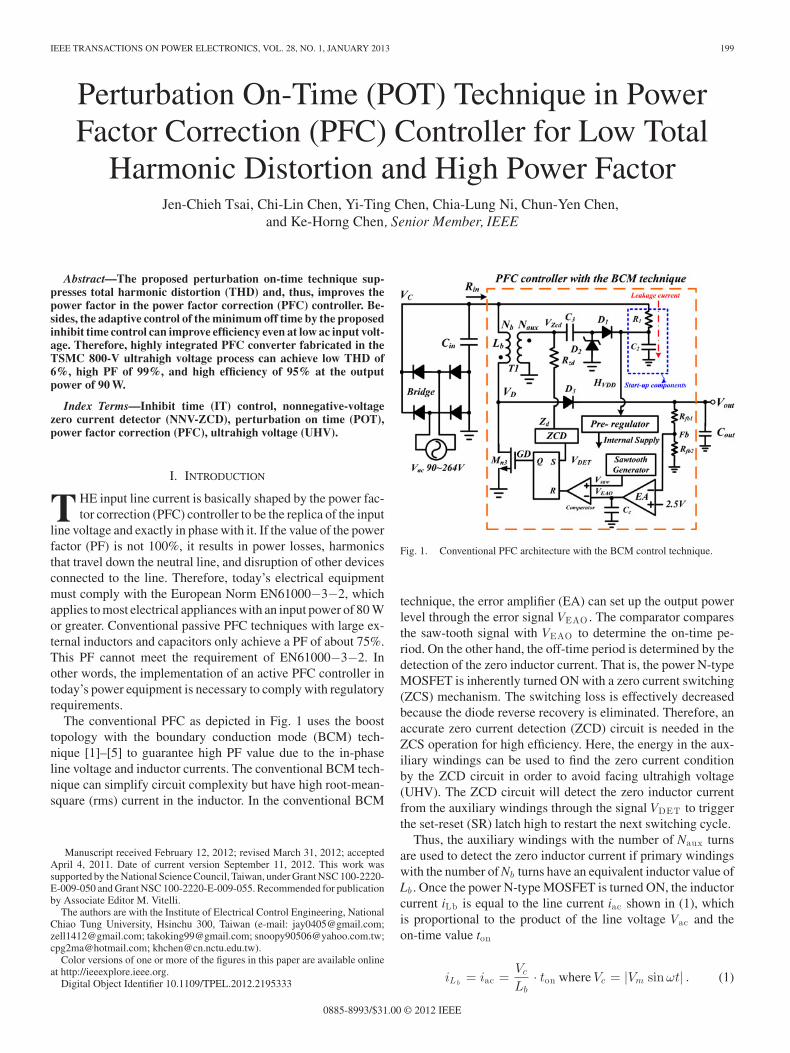
Fig. 1. Conventional PFC architecture with the BCM control technique.
technique, the error amplifier (EA) can set up the output powerlevel through the error signal VEAO . The comparator comparesthe saw-tooth signal with VEAO to determine the on-time pe-riod. On the other hand, the off-time period is determined by thedetection of the zero inductor current. That is, the power N-typeMOSFET is inherently turned ON with a zero current switching(ZCS) mechanism. The switching loss is effectively decreasedbecause the diode reverse recovery is eliminated. Therefore, anaccurate zero current detection (ZCD) circuit is needed in theZCS operation for high efficiency. Here, the energy in the aux-iliary windings can be used to find the zero current conditionby the ZCD circuit in order to avoid facing ultrahigh voltage(UHV). The ZCD circuit will detect the zero inductor currentfrom the auxiliary windings through the signal VDET to triggerthe set-reset (SR) latch high to restart the next switching cycle.
Thus, the auxiliary windings with the number of Naux turnsare used to detect the zero inductor current if primary windingswith the number of Nb turns have an equivalent inductor value ofLb . Once the power N-type MOSFET is turned ON, the inductorcurrent iLb is equal to the line current iac shown in (1), whichis proportional to the product of the line voltage Vac and theon-time value ton
iLb= iac =
Vc
Lb· ton where Vc = |Vm sinωt| . (1)
0885-8993/$31.00 © 2012 IEEE
200 IEEE TRANSACTIONS ON POWER ELECTRONICS, VOL. 28, NO. 1, JANUARY 2013
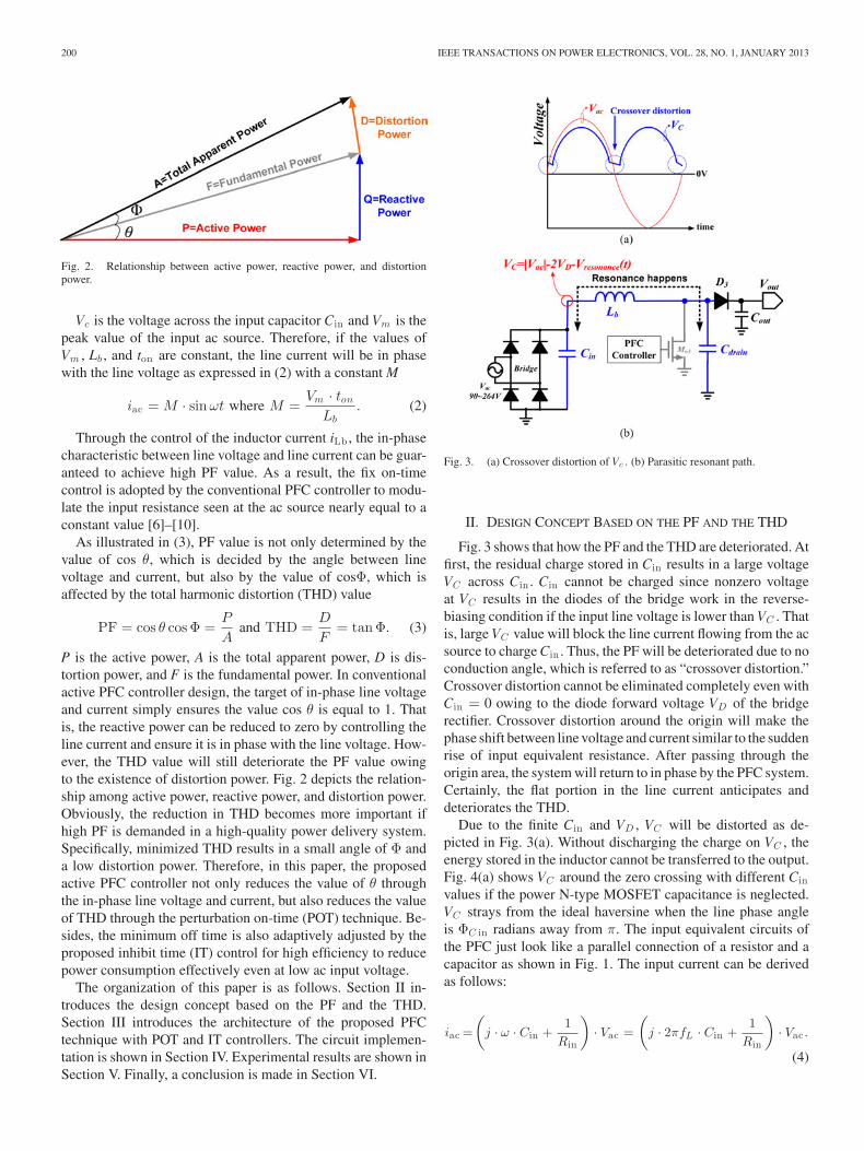
Fig. 2. Relationship between active power, reactive power, and distortionpower.
Vc is the voltage across the input capacitor Cin and Vm is thepeak value of the input ac source. Therefore, if the values ofVm , Lb , and ton are constant, the line current will be in phasewith the line voltage as expressed in (2) with a constant M
iac = M · sinωt where M =Vm · ton
Lb. (2)
Through the control of the inductor current iLb , the in-phasecharacteristic between line voltage and line current can be guar-anteed to achieve high PF value. As a result, the fix on-timecontrol is adopted by the conventional PFC controller to modu-late the input resistance seen at the ac source nearly equal to aconstant value [6]–[10].
As illustrated in (3), PF value is not only determined by thevalue of cos θ, which is decided by the angle between linevoltage and current, but also by the value of cosΦ, which isaffected by the total harmonic distortion (THD) value
PF = cos θ cos Φ =P
Aand THD =
D
F= tan Φ. (3)
P is the active power, A is the total apparent power, D is dis-tortion power, and F is the fundamental power. In conventionalactive PFC controller design, the target of in-phase line voltageand current simply ensures the value cos θ is equal to 1. Thatis, the reactive power can be reduced to zero by controlling theline current and ensure it is in phase with the line voltage. How-ever, the THD value will still deteriorate the PF value owingto the existence of distortion power. Fig. 2 depicts the relation-ship among active power, reactive power, and distortion power.Obviously, the reduction in THD becomes more important ifhigh PF is demanded in a high-quality power delivery system.Specifically, minimized THD results in a small angle of Φ anda low distortion power. Therefore, in this paper, the proposedactive PFC controller not only reduces the value of θ throughthe in-phase line voltage and current, but also reduces the valueof THD through the perturbation on-time (POT) technique. Be-sides, the minimum off time is also adaptively adjusted by theproposed inhibit time (IT) control for high efficiency to reducepower consumption effectively even at low ac input voltage.
The organization of this paper is as follows. Section II in-troduces the design concept based on the PF and the THD.Section III introduces the architecture of the proposed PFCtechnique with POT and IT controllers. The circuit implemen-tation is shown in Section IV. Experimental results are shown inSection V. Finally, a conclusion is made in Section VI.
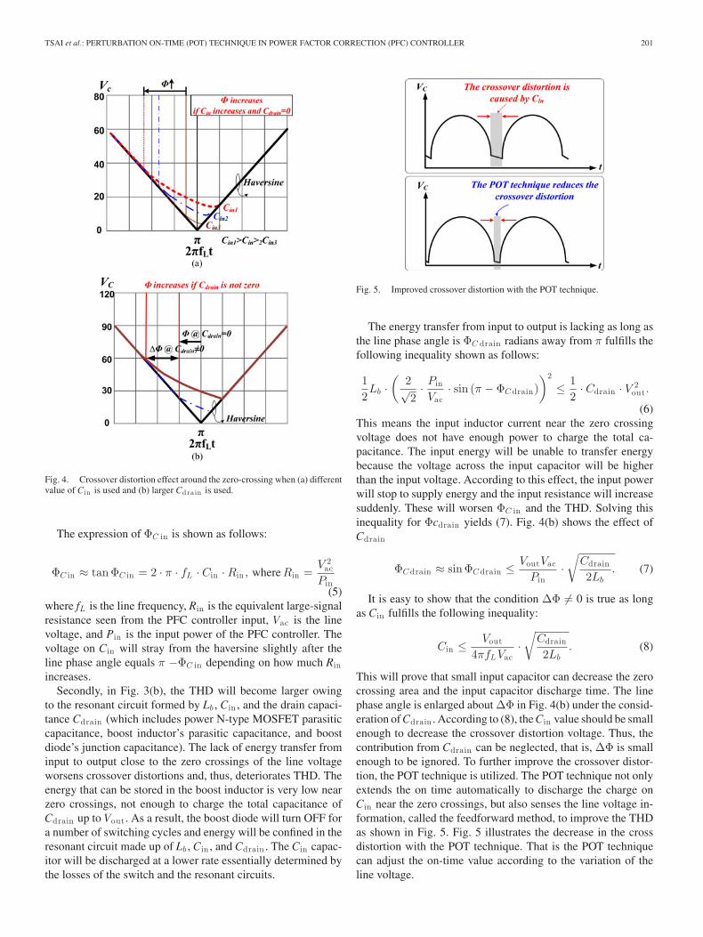
Fig. 3. (a) Crossover distortion of Vc . (b) Parasitic resonant path.
II. DESIGN CONCEPT BASED ON THE PF AND THE THD
Fig. 3 shows that how the PF and the THD are deteriorated. Atfirst, the residual charge stored in Cin results in a large voltageVC across Cin . Cin cannot be charged since nonzero voltageat VC results in the diodes of the bridge work in the reverse-biasing condition if the input line voltage is lower than VC . Thatis, large VC value will block the line current flowing from the acsource to charge Cin . Thus, the PF will be deteriorated due to noconduction angle, which is referred to as “crossover distortion.”Crossover distortion cannot be eliminated completely even withCin = 0 owing to the diode forward voltage VD of the bridgerectifier. Crossover distortion around the origin will make thephase shift between line voltage and current similar to the suddenrise of input equivalent resistance. After passing through theorigin area, the system will return to in phase by the PFC system.Certainly, the flat portion in the line current anticipates anddeteriorates the THD.
Due to the finite Cin and VD , VC will be distorted as de-picted in Fig. 3(a). Without discharging the charge on VC , theenergy stored in the inductor cannot be transferred to the output.Fig. 4(a) shows VC around the zero crossing with different Cinvalues if the power N-type MOSFET capacitance is neglected.VC strays from the ideal haversine when the line phase angleis ΦC in radians away from π. The input equivalent circuits ofthe PFC just look like a parallel connection of a resistor and acapacitor as shown in Fig. 1. The input current can be derivedas follows:
iac =
(j · ω · Cin +
1Rin
)· Vac =
(j · 2πfL · Cin +
1Rin
)· Vac .
(4)
TSAI et al.: PERTURBATION ON-TIME (POT) TECHNIQUE IN POWER FACTOR CORRECTION (PFC) CONTROLLER 201
Fig. 4. Crossover distortion effect around the zero-crossing when (a) differentvalue of Cin is used and (b) larger Cdrain is used.
The expression of ΦC in is shown as follows:
ΦC in ≈ tan ΦC in = 2 · π · fL · Cin · Rin , where Rin =V 2
ac
Pin(5)
where fL is the line frequency, Rin is the equivalent large-signalresistance seen from the PFC controller input, Vac is the linevoltage, and Pin is the input power of the PFC controller. Thevoltage on Cin will stray from the haversine slightly after theline phase angle equals π −ΦC in depending on how much Rinincreases.
Secondly, in Fig. 3(b), the THD will become larger owingto the resonant circuit formed by Lb , Cin , and the drain capaci-tance Cdrain (which includes power N-type MOSFET parasiticcapacitance, boost inductor’s parasitic capacitance, and boostdiode’s junction capacitance). The lack of energy transfer frominput to output close to the zero crossings of the line voltageworsens crossover distortions and, thus, deteriorates THD. Theenergy that can be stored in the boost inductor is very low nearzero crossings, not enough to charge the total capacitance ofCdrain up to Vout . As a result, the boost diode will turn OFF fora number of switching cycles and energy will be confined in theresonant circuit made up of Lb , Cin , and Cdrain . The Cin capac-itor will be discharged at a lower rate essentially determined bythe losses of the switch and the resonant circuits.
Fig. 5. Improved crossover distortion with the POT technique.
The energy transfer from input to output is lacking as long asthe line phase angle is ΦC drain radians away from π fulfills thefollowing inequality shown as follows:
12Lb ·
(2√2· Pin
Vac· sin (π − ΦC drain)
)2
≤ 12· Cdrain · V 2
out .
(6)This means the input inductor current near the zero crossingvoltage does not have enough power to charge the total ca-pacitance. The input energy will be unable to transfer energybecause the voltage across the input capacitor will be higherthan the input voltage. According to this effect, the input powerwill stop to supply energy and the input resistance will increasesuddenly. These will worsen ΦC in and the THD. Solving thisinequality for Φcdrain yields (7). Fig. 4(b) shows the effect ofCdrain
ΦC drain ≈ sin ΦC drain ≤ VoutVac
Pin·√
Cdrain
2Lb. (7)
It is easy to show that the condition ΔΦ �= 0 is true as longas Cin fulfills the following inequality:
Cin ≤ Vout
4πfLVac·√
Cdrain
2Lb. (8)
This will prove that small input capacitor can decrease the zerocrossing area and the input capacitor discharge time. The linephase angle is enlarged about ΔΦ in Fig. 4(b) under the consid-eration of Cdrain . According to (8), the Cin value should be smallenough to decrease the crossover distortion voltage. Thus, thecontribution from Cdrain can be neglected, that is, ΔΦ is smallenough to be ignored. To further improve the crossover distor-tion, the POT technique is utilized. The POT technique not onlyextends the on time automatically to discharge the charge onCin near the zero crossings, but also senses the line voltage in-formation, called the feedforward method, to improve the THDas shown in Fig. 5. Fig. 5 illustrates the decrease in the crossdistortion with the POT technique. That is the POT techniquecan adjust the on-time value according to the variation of theline voltage.

202 IEEE TRANSACTIONS ON POWER ELECTRONICS, VOL. 28, NO. 1, JANUARY 2013
Fig. 6. Conventional PFC input ac current at (a) heavy loads and (b) lightloads.
III. PROPOSED PFC CONTROLLER WITH THE POTAND THE IT TECHNIQUES
A. POT Technique
The conventional BCM architecture is as shown in Fig. 1.The expressions of on time ton and off time toff are shown asfollows:
ton =VEAO
Vsaw· TS and toff =
Vc
Vout − Vc· ton (9)
where
TS = ton + toff . (10)
As shown in Fig. 6(a), the well-regulated dc output voltageensures the value on time is nearly constant to derive the inputresistance seen at the ac source nearly constant for high PF. Asmentioned earlier, the THD will deteriorate the PF [11]–[13].In (11), THD is also commonly defined as the ratio of the sumof the powers of all harmonic components to the power of thefundamental frequency, where I1 is the fundamental signal ofiac and I2–In indicate the harmonic signals of iac
THD =
√I22 + I2
3 + I24 + I2
5 + . . . . . . + I2n
I1. (11)
The THD gradually increases when the output loading de-creases as depicted in Fig. 6(b) because the fundamental energyis decreased. Thus, the PF is seriously affected.
Ideally, the PF is equal to the following expression
PF =Pin
Pline=
(1/2π) ·∫ 2π
0 iac (θ) · vac (θ) · dθ
Irms · Vrms. (12)
Pin is the input power and Pline is the line power. Irms and Vrmsare the rms value of the line current and voltage, respectively.
If the crossover distortion caused by the voltage drop of thediodes and the resonant effect in the bridge is considered, theTHD is further deteriorated. The main crossover distortion angleΦ caused by the THD will be proved as follows. That is, the linecurrent can be expressed as (13) if Φ is taken into consideration,where Im is the peak value of the line current
iac (θ) =Im
1 − sin Φ· (sin θ − sin Φ) and vac(θ) = Vm sin θ.
(13)As a result, Pin (θ) with the consideration of the THD effect
can be derived as (14) after substituting (13) into (12)
Pin (θ) =Vm · Im
π · (1 − sin Φ)·[π
2− Φ − 1
2sin 2Φ
]. (14)
When the crossover distortion angle is smaller than Φ, the inputline current is zero. Hence, the distortion angle is only provedfrom Φ to π − Φ with Pin given by (14). Here, Irms can bederived as follows:
Irm s =
√12π
·∫ 2π
0
i2ac (θ) · dθ
=
√I2
m
π · (1 − sin Φ)2 ·[π
2− Φ − 3
2sin 2Φ + (π − 2Φ) sin2 Φ
].
(15)
Therefore, the PF and the THD can be obtained as follows:
PF(Φ) =Pi
Vrms · Irms
=π − 2Φ − sin 2Φ√
π · [(π − 2Φ) (2 − 2 cos 2Φ) − (3 sin 2Φ)](16)
THD(Φ)% = 100
·√
π · [(π − 2Φ) (2 − 2 cos 2Φ) − (3 sin 2Φ)](π − 2Φ − sin 2Φ)2 − 1. (17)
The THD is seriously affected by the distortion angle Φ. Byreducing the value of Φ, the THD can be decreased and thus thePF can be effectively improved. If the value of Φ can be greatlydecreased, (16) and (17) can be simplified as follows:
PF(Φ) =π − 2Φ√
π · (π − 2Φ)(18)
THD(Φ)% = 100 ·√
π
(π − 2Φ)− 1. (19)
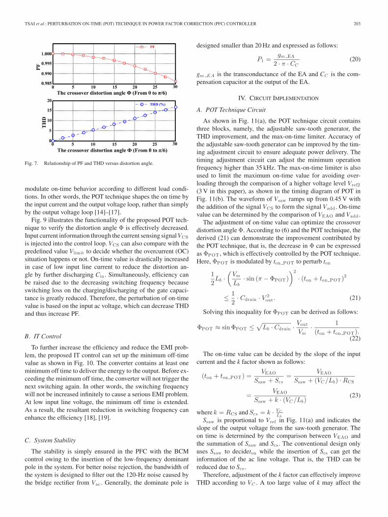
Fig. 7 illustrates the variations of PF and THD versus the varia-tions of crossover distortion angle effect. The smaller the valueof Φ, the better it will correspond to the values of PF and THD.Therefore, if the THD needs to be smaller than 5%, the valueof Φ should be smaller than 0.08 rd/s. As a result, it will have ahigh PF value of 0.999.
Fig. 8 shows the proposed PFC architecture with POT and ITcontrols for reduced THD and high PF at the same time. ThePOT technique modifies the conventional fix on-time mech-anism through the addition of input current information to
TSAI et al.: PERTURBATION ON-TIME (POT) TECHNIQUE IN POWER FACTOR CORRECTION (PFC) CONTROLLER 203
Fig. 7. Relationship of PF and THD versus distortion angle.
modulate on-time behavior according to different load condi-tions. In other words, the POT technique shapes the on time bythe input current and the output voltage loop, rather than simplyby the output voltage loop [14]–[17].
Fig. 9 illustrates the functionality of the proposed POT tech-nique to verify the distortion angle Φ is effectively decreased.Input current information through the current sensing signal VCSis injected into the control loop. VCS can also compare with thepredefined value Vlimit to decide whether the overcurrent (OC)situation happens or not. On-time value is drastically increasedin case of low input line current to reduce the distortion an-gle by further discharging Cin . Simultaneously, efficiency canbe raised due to the decreasing switching frequency becauseswitching loss on the charging/discharging of the gate capaci-tance is greatly reduced. Therefore, the perturbation of on-timevalue is based on the input ac voltage, which can decrease THDand thus increase PF.
B. IT Control
To further increase the efficiency and reduce the EMI prob-lem, the proposed IT control can set up the minimum off-timevalue as shown in Fig. 10. The converter contains at least oneminimum off time to deliver the energy to the output. Before ex-ceeding the minimum off time, the converter will not trigger thenext switching again. In other words, the switching frequencywill not be increased infinitely to cause a serious EMI problem.At low input line voltage, the minimum off time is extended.As a result, the resultant reduction in switching frequency canenhance the efficiency [18], [19].
C. System Stability
The stability is simply ensured in the PFC with the BCMcontrol owing to the insertion of the low-frequency dominantpole in the system. For better noise rejection, the bandwidth ofthe system is designed to filter out the 120-Hz noise caused bythe bridge rectifier from Vac . Generally, the dominate pole is
designed smaller than 20 Hz and expressed as follows:
P1 =gm EA
2 · π · CC(20)
gm EA is the transconductance of the EA and CC is the com-pensation capacitor at the output of the EA.
IV. CIRCUIT IMPLEMENTATION
A. POT Technique Circuit
As shown in Fig. 11(a), the POT technique circuit containsthree blocks, namely, the adjustable saw-tooth generator, theTHD improvement, and the max-on-time limiter. Accuracy ofthe adjustable saw-tooth generator can be improved by the tim-ing adjustment circuit to ensure adequate power delivery. Thetiming adjustment circuit can adjust the minimum operationfrequency higher than 35 kHz. The max-on-time limiter is alsoused to limit the maximum on-time value for avoiding over-loading through the comparison of a higher voltage level Vref2(3 V in this paper), as shown in the timing diagram of POT inFig. 11(b). The waveform of Vsaw ramps up from 0.45 V withthe addition of the signal VCS to form the signal Vadd . On-timevalue can be determined by the comparison of VEAO and Vadd .
The adjustment of on-time value can optimize the crossoverdistortion angle Φ. According to (6) and the POT technique, thederived (21) can demonstrate the improvement contributed bythe POT technique, that is, the decrease in Φ can be expressedas ΦPOT , which is effectively controlled by the POT technique.Here, ΦPOT is modulated by ton POT to perturb ton
12Lb ·
(Vm
Lb· sin (π − ΦPOT)
)2
· (ton + ton POT)2
≤ 12· Cdrain · V 2
out . (21)
Solving this inequality for ΦPOT can be derived as follows:
ΦPOT ≈ sin ΦPOT ≤√
Lb · Cdrain · Vout
Vm· 1(ton + ton POT).
(22)
The on-time value can be decided by the slope of the inputcurrent and the k factor shown as follows:
(ton + ton POT) =VEAO
Ssaw + Scs=
VEAO
Ssaw + (VC /Lb) · RCS
=VEAO
Ssaw + k · (VC /Lb)(23)
where k = RCS and Scs = k · VC
Lb
Ssaw is proportional to Vref in Fig. 11(a) and indicates theslope of the output voltage from the saw-tooth generator. Theon time is determined by the comparison between VEAO andthe summation of Ssaw and Scs . The conventional design onlyuses Ssaw to decideton while the insertion of Scs can get theinformation of the ac line voltage. That is, the THD can bereduced due to Scs .
Therefore, adjustment of the k factor can effectively improveTHD according to VC . A too large value of k may affect the
204 IEEE TRANSACTIONS ON POWER ELECTRONICS, VOL. 28, NO. 1, JANUARY 2013
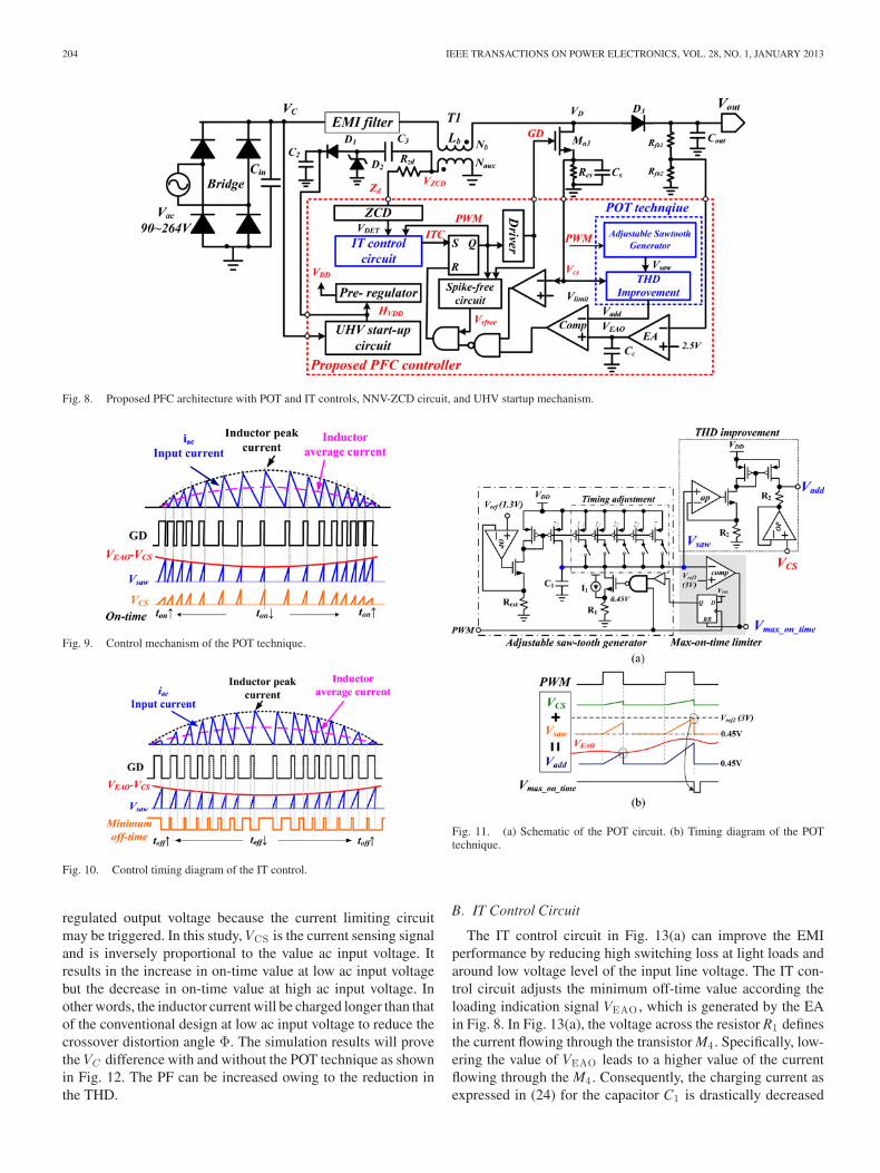
Fig. 8. Proposed PFC architecture with POT and IT controls, NNV-ZCD circuit, and UHV startup mechanism.
Fig. 9. Control mechanism of the POT technique.
Fig. 10. Control timing diagram of the IT control.
regulated output voltage because the current limiting circuitmay be triggered. In this study, VCS is the current sensing signaland is inversely proportional to the value ac input voltage. Itresults in the increase in on-time value at low ac input voltagebut the decrease in on-time value at high ac input voltage. Inother words, the inductor current will be charged longer than thatof the conventional design at low ac input voltage to reduce thecrossover distortion angle Φ. The simulation results will provethe VC difference with and without the POT technique as shownin Fig. 12. The PF can be increased owing to the reduction inthe THD.
Fig. 11. (a) Schematic of the POT circuit. (b) Timing diagram of the POTtechnique.
B. IT Control Circuit
The IT control circuit in Fig. 13(a) can improve the EMIperformance by reducing high switching loss at light loads andaround low voltage level of the input line voltage. The IT con-trol circuit adjusts the minimum off-time value according theloading indication signal VEAO , which is generated by the EAin Fig. 8. In Fig. 13(a), the voltage across the resistor R1 definesthe current flowing through the transistor M4 . Specifically, low-ering the value of VEAO leads to a higher value of the currentflowing through the M4 . Consequently, the charging current asexpressed in (24) for the capacitor C1 is drastically decreased
TSAI et al.: PERTURBATION ON-TIME (POT) TECHNIQUE IN POWER FACTOR CORRECTION (PFC) CONTROLLER 205
Fig. 12. Waveform of VC with and without the POT technique.
Fig. 13. (a) Schematic of the IT control circuit. The timing diagram of the ITcontrol circuit at (b) light loads and (c) heavy loads.
to generate a longer minimum off time
IC1 = Ibias − k1 · k2 ·Vref − VEAO
R1(24)
where k1 and k2 are current mirror ratios.The timing diagram of the IT control circuit is shown in
Fig. 13(b) and (c) at light loads and heavy loads, respectively.
C. Nonnegative-Voltage Zero Current Detector Circuit
The BCM operation is depicted in Fig. 14(a) and (b) to showthe inductor charge and discharge path, respectively, for reveal-ing VZCD potential. The timing diagram of the ZCD operationin BCM control is shown in Fig. 15. The BCM is used in theZCS technique. As the inductor energy releases to the output,the switch-on point is selected at the next zero-crossing pointafter tdis because the inductor current is close to zero in theBCM operation. If the inductor current reaches zero, the nextswitching cycle will be triggered to effectively deliver energy tothe output. In the meanwhile, VZCD decreases toward a negativevalue equal to − (Naux/Nb) · VC , that is, the ratio of auxiliary
Fig. 14. Operation of the conventional PFC with the BCM control. (a) On-time is determined by the peak current control. (b) Off-time is determined bythe ZCD.
Fig. 15. ZCD waveforms with the proposed nonnegative signal Zd .
winding to the primary winding determines how negative thevalue of VZCD is. However, if the signal of VZCD as expressedin (25) is injected to the controller chip, it will result in thefailure of the chip owing to the latch-up problem, which causespermanent damage
−(
Naux
Nb
)· VC ≤ VZCD ≤
(Naux
Nb
)· (VD − VC ) . (25)
Therefore, instead of VZCD , the filtered signal Zd generated bythe proposed nonnegative-voltage zero current detector (NNV-ZCD) circuit in Fig. 16 is clamped between Vclamp low andVclamp high to avoid negative voltage and overvoltage, respec-tively. When the PWM signal switches from high to low, thestored energy of the inductor starts to release to the output.VZCD will start to decrease because the energy in the inductordries out. Once the signal Zd voltage is lower than the thresholdvoltage VH , the PWM signal will be set high by the positive trig-gering signal VDET to start the next switching cycle. The signalVDET will be reset as the Zd signal is lower than VL . WhenZd gradually decreases smaller than zero, the transistor M2 will

206 IEEE TRANSACTIONS ON POWER ELECTRONICS, VOL. 28, NO. 1, JANUARY 2013
Fig. 16. Schematic of the proposed NNV-ZCD circuit.
Fig. 17. Timing diagram of the proposed NNV-ZCD circuit.
form a negative feedback to clamp the voltage still higher than0.8 V. The low clamping voltage Vclamp low , 0.8 V, is used to de-tect the high-to-low transition of VZCD to prevent the chip fromseeing the negative voltage. Ideally, the value should be 0 V.However, considering the PVT variations, the value is raised to0.8 V to have a tolerance margin due to the response time of thesensing circuit. The timing diagram is shown in Fig. 17.
The next switching cycle will start the peak current controlafter setting the signal gate driver (GD) to high by the PWMsignal. Here, to improve the switching noise immunity, the cur-rent sensing signal is blocked until the signal Vsfree from thespike-free circuit is set to high.
D. UHV Startup Circuit
Before the first stable switching, no power can be deliveredto auxiliary winding. Therefore, the PFC control circuit needsthe startup circuit to guarantee the initial of the preregulator.After the preregulator obtained the ability to supply the PFCcontroller to start the BCM operation, the startup circuit will beshut down to save much power loss. In Fig. 1, the conventionalstartup mechanism contains the external startup resistor and thehold-up capacitor, R1 and C2 , respectively. R1 is 470 k and con-sumes 0.18 W at 220 Vac . The charge pump circuit, composedwith D1 , D2 , and C3 , can supply the hold-up voltage for theinternal preregulator once the BCM operation starts to work.However, the external startup resistor and capacitor (R1 and C2 ,respectively) will induce a large leakage current even after thestartup period because the passive components cannot be shutdown. Efficiency is greatly deteriorated by such a simple startupmechanism.
Fig. 18. Schematic of the 800 V UHV startup circuit.
Fig. 19. Schematic of the spike-free circuit at (a) timing diagram at (b) heavyloads and (c) light loads.
In contrast, the proposed UHV startup technique in Fig. 8can ensure the initial of the preregulator during the power-onperiod [20], which can be fully shut down for power saving oncethe auxiliary winding of the transformer can provide enoughenergy to the hold-up capacitor C2 to have a regulated HVDD .Moreover, the number of external passive components can bereduced for low cost and compact size.
The 800-V UHV startup circuit is depicted in Fig. 18. TheUHV startup function can be implemented using one UHV de-pletion N-type MOSFET MUHV . The UHV startup circuit hasa hysteric window that will be generated by M1 to reject powernoise. The upper bound and lower bound voltages are shown asfollows:
HVDD(upper bound) =R1 + R2
R2· VTH2 and HVDD(lower bound)
=R1 + R2 + R3
R2 + R3· VTH2 . (26)

TSAI et al.: PERTURBATION ON-TIME (POT) TECHNIQUE IN POWER FACTOR CORRECTION (PFC) CONTROLLER 207
TABLE IDESIGN SPECIFICATIONS
TABLE IICOMPARISONS ARE BETWEEN THE PROPOSED METHOD AND THE PRIOR ARTS
Fig. 20. Micrograph of the PFC circuit with the POT technique, the IT controlcircuit, and the UHV startup mechanism.
During the power-on sequence, the UHV transistor will beturned OFF by M2 when HVDD is higher than the upper boundvoltage. Due to the shutdown of the UHV transistor, the leakagecurrent can be minimized. If the voltage at the output capaci-tor C2 is lower than the lower bound voltage, the UHV startupcircuit is triggered again.
Fig. 21. Cross sections in UHV lateral power LDMOS with triple RESURFstructure.
E. Spike-Free Circuit
Owing to high current flowing through the power MOSFETMn 3 in Fig. 8, the spike-free circuit is used to evade the spikenoise and avoid an abnormal decision of the duty cycle. Thespike-free circuit is shown in Fig. 19(a) can avoid the highswitching noise issue when the power MOSFET is turned ON.Simultaneously, the current limiting mechanism will be disabledduring the spike-free operation in order not to shut down theoverall operation. The spike-free circuit eliminates the switchingnoise issue spike without needing an external low pass filter.
208 IEEE TRANSACTIONS ON POWER ELECTRONICS, VOL. 28, NO. 1, JANUARY 2013
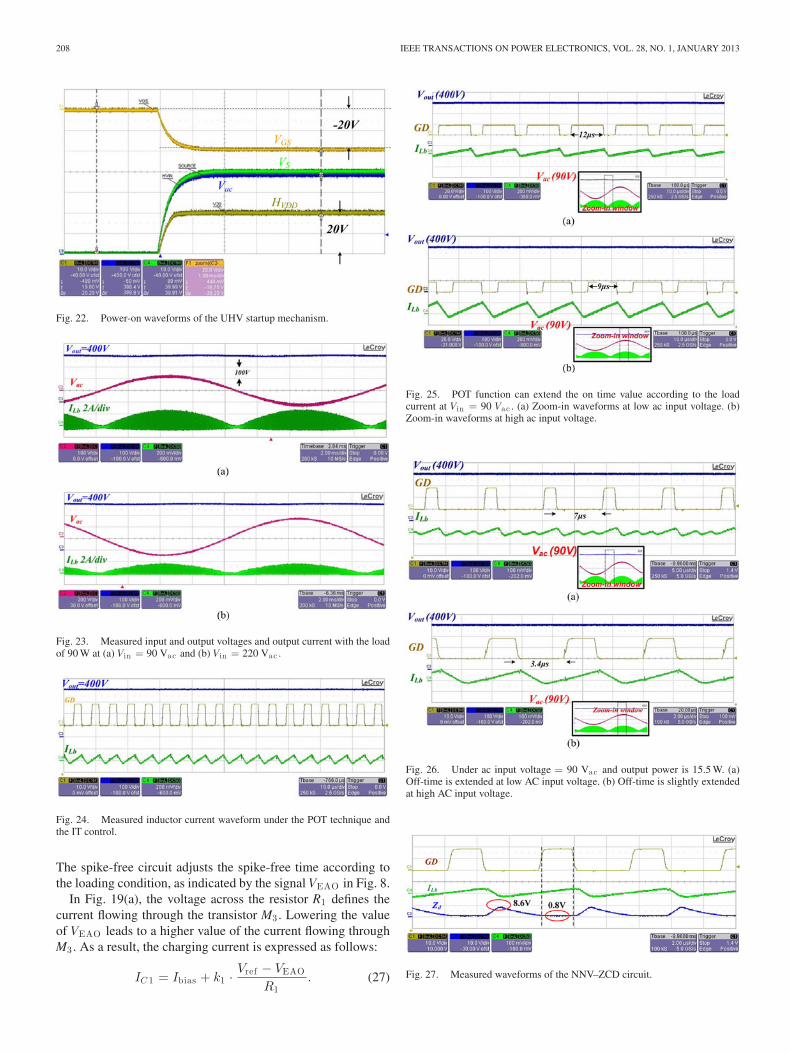
Fig. 22. Power-on waveforms of the UHV startup mechanism.
Fig. 23. Measured input and output voltages and output current with the loadof 90 W at (a) Vin = 90 Vac and (b) Vin = 220 Vac .
Fig. 24. Measured inductor current waveform under the POT technique andthe IT control.
The spike-free circuit adjusts the spike-free time according tothe loading condition, as indicated by the signal VEAO in Fig. 8.
In Fig. 19(a), the voltage across the resistor R1 defines thecurrent flowing through the transistor M3 . Lowering the valueof VEAO leads to a higher value of the current flowing throughM3 . As a result, the charging current is expressed as follows:
IC 1 = Ibias + k1 ·Vref − VEAO
R1. (27)
Fig. 25. POT function can extend the on time value according to the loadcurrent at Vin = 90 Vac . (a) Zoom-in waveforms at low ac input voltage. (b)Zoom-in waveforms at high ac input voltage.
Fig. 26. Under ac input voltage = 90 Vac and output power is 15.5 W. (a)Off-time is extended at low AC input voltage. (b) Off-time is slightly extendedat high AC input voltage.
Fig. 27. Measured waveforms of the NNV–ZCD circuit.

TSAI et al.: PERTURBATION ON-TIME (POT) TECHNIQUE IN POWER FACTOR CORRECTION (PFC) CONTROLLER 209
Fig. 28. (a) Measured EMI results of the PFC controller without the IT technique and with the IT technique under the same EMI filter. (b) EMI filter used in thispaper.
The timing diagram of the spike-free circuit is shown inFig. 19(b) and (c) at heavy and light loads, respectively. Thevalue of the spike-free period is extended at heavy loads due tothe large switching noise caused by a large inductor current.
V. EXPERIMENT RESULTS
The PFC controller with the POT technique and the IT con-trol circuit, the NNV-ZCD circuit, and the UHV startup mecha-nism was fabricated in the TSMC 0.5 μm 800-V UHV LDMOSprocess. The specifications of the PFC controller are listed inTable I and the comparison with the prior arts is also shown inTable II. The figure of merit (FOM) shown in (28) can comparethe performance among different implementations
FOM =Lb · Cout · THD
PF. (28)
The proposed technique can have the minimum FOM comparedto the others. That is, the system can have a small volume andimproved performance compared to the others.
The external devices of the primary-side inductor and theoutput capacitor are 400 and 68 μF, respectively. Consideringthe preregulator as the internal power supply, the upper-boundstartup voltage is 16 V. Output voltage of the PFC controller is400 V for the next-stage PWM converter.
The chip micrograph is shown in Fig. 20 with an active areaof 1200 μm × 800 μm. A conventional cross section of theUHV triple reduce surface field (RESURF) lateral MOSFET(LDMOS) is shown in Fig. 21. The contact of n-drift and p-well can resist high voltage. Furthermore, the structure withfloating p buried well inserted into n drift region to providedual conduction paths that can provide a significant reductionin on-state resistance [23]. The power-on sequence of the UHVstartup mechanism is shown in Fig. 22. The output voltageHVDD is 20 V and the final VGS of the UHV device is −20 V.That is, the depletion NMOSFET is completely turned OFF forlow leakage current.
Fig. 29. Measured THD performance with and without the POT technique atfull load condition.
Fig. 23 shows the measured waveforms at full load at 90 Vacand 220 Vac input voltages, respectively. Vout is regulated at400 V with the load of 90 W. The PF is 0.998 and 0.985, re-spectively. The measured inductor current shows the POT andIT operations in Fig. 24. Fig. 25(a) shows the function of thePOT circuit to extend the on-time value at low ac input voltage.The on-time value will be extended at zero current condition toimprove THD value automatically. Fig. 25(b) shows the POT ontime at high ac input voltage. Thus, the PF is 0.998 contributedby the POT technique. Fig. 26(a) shows the function of the ITcontroller to reduce switching loss at the low ac input voltage.The zero current is detected, but the next PWM signal is trig-gered when the inhibit off time is over. Fig. 26(b) shows theIT is smaller than the off-time value. Thus, the zero current de-termines the beginning of the next PWM signal. The estimatedefficiency is 95% due to the POT and IT controls.
Fig. 27 shows the measured waveforms of the NNV-ZCDcircuit. When the power N-type MOSFET is turned ON, themaximum input signal Zd is clamped to 8.6 V, not the calculated
210 IEEE TRANSACTIONS ON POWER ELECTRONICS, VOL. 28, NO. 1, JANUARY 2013
Fig. 30. Measured efficiency results of the PFC controller. (a) 90 Vac . (b) 220 Vac .
Fig. 31. Measured results improved by the POT technique. (a) PF value. (b) THD value.
value of 53.3 V. On the other hand, the minimum input signalZd is clamped to 0.8 V, not the calculated value of −49.77 V.Vclamp high was locked by the zener diode and Vclamp low wasreached almost 0.8 V by negative feedback technique in theNNV circuit. The nonnegative Zd can prevent the integrated chipfrom being damaged by the large negative voltage. Fig. 28(a)shows the experimental EMI in the two cases: with and withoutIT enabled. The EMI can be effectively improved by the pro-posed technique with the same EMI filter in Fig. 28(b). Besides,under the requirement of EN61000−3−2, the proposed methodcan reduce the EMI filter (Cπ1 , Lπ , and Cπ2) from the conven-tional design (0.47, 350, and 0.47 μF) to the new value (0.33,280, and 0.33 μF).
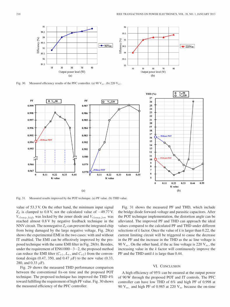
Fig. 29 shows the measured THD performance comparisonbetween the conventional fix-on time and the proposed POTtechnique. The proposed technique has improved the THD 4%toward fulfilling the requirement of high PF value. Fig. 30 showsthe measured efficiency of the PFC controller.
Fig. 31 shows the measured PF and THD, which includethe bridge diode forward-voltage and parasitic capacitors. Afterthe POT technique implementation, the distortion angle can bealleviated. The improved PF and THD can approach the idealvalues compared to the calculated PF and THD under differentselections of k factor. Once the value of k is larger than 0.22, thecurrent limiting circuit will be triggered to cause the decreasein the PF and the increase in the THD as the ac line voltage is90 Vac . On the other hand, if the ac line voltage is 220 Vac , theincreasing value in the k factor will continuously improve thePF and the THD until k is large than 0.44.
VI. CONCLUSION
A high efficiency of 95% can be ensured at the output powerof 90 W through the proposed POT and IT controls. The PFCcontroller can have low THD of 6% and high PF of 0.998 at90 Vac, and high PF of 0.985 at 220 Vac because the on-time

TSAI et al.: PERTURBATION ON-TIME (POT) TECHNIQUE IN POWER FACTOR CORRECTION (PFC) CONTROLLER 211
value is perturbed by the input voltage information for reducingthe distortion angle. The adaptive minimum off-time adjustmentby the IT controller can also reduce the switching power loss toguarantee high efficiency. In addition, due to the UHV device,the startup mechanism can minimize the current leakage at theac input and remove the need of external startup components.Thus, the performance can be further enhanced under the im-proved noise immunity by the spike-free circuit. The test circuitfabricated in the TSMC 800-V UHV process can show highperformance and a highly integrated PFC controller.
ACKNOWLEDGMENT
The authors would like to thank Realtek Semiconductor Cor-poration for their help.
REFERENCES
[1] R. W. Erickson and D. Maksimovic, Fundamentals of Power Electronics,2nd ed. Norwell, MA: Kluwer Academic Publishers, 2001.
[2] J. W. Kim, S. M. Choi, and K. T. Kim, “Variable on-time control ofthe critical conduction mode boost power factor correction converter toimprove zero-crossing distortion,” Power Electron. Drives Syst., vol. 2,pp. 1542–1546, Nov. 2005.
[3] Y.-S. Roh, Y.-J. Moon, J.-C. Gong, and C. Yoo, “Active power factorcorrection (PFC) circuit with resistor-free zero-current detection,” IEEETrans. Power Electron., vol. 26, no. 2, pp. 630–637, Feb. 2011.
[4] Y. Wang, Y. Zhang, Q. Mo, M. Chen, and Z. Qian, “An improved controlstrategy based on multiplier for CRM flyback PFC to reduce line currentpeak distortion,” in Proc. IEEE Energy Convers. Congr. Expo., Sep. 2010,pp. 901–905.
[5] “Design of Power Factor Correction Circuit Using FAN7527B” Fairchildapplication note AN4121.
[6] J.-S. Lai and D. Chen, “Design consideration for power factor correctionboost converter operating at the boundary of continuous conduction modeand discontinuous conduction mode,” in IEEE Appl. Power Electron.Conf., Mar. 1993, pp. 267–273.
[7] K. Yao, X. Ruan, X. Mao, and Z. Ye, “Variable-duty-cycle control toachieve high input power factor for DCM boost PFC converter,” IEEETrans. Ind. Electron., vol. 58, no. 5, pp. 1856–1865, May 2011.
[8] Power Factor Correction Handbook, ON Semiconductor, Phoenix, AZ,Sep. 2007.
[9] P. Preller, “A controller family for switch mode power supplies supportinglow power standby and power factor correction,” Infineon Technol. AG,Munich, Germany, Appl. Note AN-TDA 1684X, Jun. 2000.
[10] J. Sebastian, J. A. Cobos, J. M. Lopera, and J. Uceda, “The determinationof the boundaries between continuous and discontinuous modes in PWMdc-to-dc converters used as power factor preregulators,” IEEE Trans.Power Electron., vol. 10, no. 5, pp. 574–582, Sep. 1995.
[11] D. S. L. Simonetti, J. L. F. Vieira, and G. C. D. Sousa, “Modeling ofthe high-power factor discontinuous boost rectifier,” IEEE Trans. Ind.Electron., vol. 46, no. 4, pp. 788–795, Aug. 1999.
[12] A. Abramovitz, “Effect of the ripple current on power factor of CRMboost APFC,” in Proc. CES/IEEE Int. Power Electron. Motion ControlConf., Aug. 2006, pp. 1412–1415.
[13] M. M. Jovanovic and Y. Jang, “State-of-the-art, single-phase, active power-factor-correction techniques for high-power applications—An overview,”IEEE Trans. Ind. Electron., vol. 52, no. 3, pp. 701–708, Jun. 2005.
[14] J. Zhang, J. Shao, F. C. Lee, and M. M. Jovanovic, “Evaluation of inputcurrent in the critical mode boost PFC converter for distributed powersystems,” in Proc. IEEE Appl. Power Electron. Conf., Feb., 2001, pp. 130–136.
[15] K. De Gusseme, D. M. Van de Sype, A. P. M. Van Den Bossche, and J.A. Melkebeek, “Input-current distortion of CCM boost PFC convertersoperated in DCM,” IEEE Trans. Ind. Electron., vol. 54, no. 2, pp. 858–865, Apr. 2007.
[16] K. H. Liu and Y. L. Lin, “Current waveform distortion in power factorcorrection circuits employing discontinuous-mode boost converters,” inProc. IEEE Power Electron. Spec. Conf., Jun. 1989, pp. 825–829.
[17] C. Y. Bernd, R. Liang, “Power factor correction with reduced total har-monic distortion,” United States Patent 6 128 205, Oct. 3, 2000.
[18] L. Huber, B. T. Irving, and M. M. Jovanovic, “Effect of valley switch-ing and switching-frequency limitation on line-current distortions ofDCM/CCM boundary boost PFC converters,” IEEE Trans. Power Elec-tron., vol. 24, no. 2, pp. 339–347, Feb. 2009.
[19] Y. Panov and M. M. Jovanovic, “Adaptive off-time control for variable-frequency, soft-switched flyback converter at light loads,” IEEE Trans.Power Electron., vol. 17, no. 4, pp. 596–603, Jul. 2002.
[20] W. Langeslag, R. Pagano, K. Schetters, A. Strijker, and A. Zoest, “VLSIdesign and application of a high-voltage-compatible SoC-ASIC in bipo-lar CMOS/DMOS technology for AC-DC rectifiers,” IEEE Trans. Ind.Electron., vol. 54, no. 5, pp. 2626–2641, Oct. 2007.
[21] S. F. Lim and A. M. Khambadkone, “A simple digital DCM control schemefor boost PFC operating in both CCM and DCM,” IEEE Trans. Ind. Appl.,vol. 47, no. 4, pp. 1802–1812, Jul./Aug. 2011.
[22] J.-W. Shin, B.-H. Cho, and J.-H. Lee, “Average current mode controlin digitally controlled discontinuous-conduction-mode PFC rectifier forimproved line current distortion,” in Proc. IEEE Appl. Power Electron.Conf. Expo., Mar., 2011, pp. 71–77.
[23] R. Y. Su, F. J. Yang, J. L. Tsay, C. C. Cheng, R. S. Liou, and H.C. Tuan, “State-of-the-art device in high voltage power ICs with low-est on-state resistance,” in Proc. IEEE Int. Electron Devices Meet., Dec.,2010, pp. 20.8.1–20.8.4.
Jen-Chieh Tsai received the B.S. degree in the De-partment of Electrical Engineering, National YunlinUniversity of Science and Technology, Yunlin, China,in 2003, and the M.S. degrees in the Department ofElectrical Engineering, Tamkang University, Taipei,Taiwan, in 2005, and is currently working toward thePh.D. degree in the Institute of Electrical Control En-gineering, National Chiao Tung University, Hsinchu,Taiwan.
He is a Faculty Member at the Mixed-Signal andPower Management IC Laboratory, Institute of Elec-
trical Control Engineering, National Chiao Tung University. His research areacontains many projects on high resolution ADC, low power DAC, and powermanagement ICs at low power mixed signal lab now. His research interests in-clude power management circuit designs, PFC ICs, and analog integrated circuitdesigns.
Chi-Lin Chen received the B.S. degree in the Depart-ment of Electrical Engineering, Yuan Ze University,Taoyuan, Taiwan, in 1995, and the M.S. degree inthe Department of Electrical Engineering, NationalCentral University, Jhongli, Taiwan, in 1998. He iscurrently working toward the Ph.D. degree in theInstitute of Electrical Control Engineering, NationalChiao Tung University, Hsinchu, Taiwan.
He is a Faculty Member at the Mixed-Signal andPower Management IC Laboratory, Institute of Elec-trical Control Engineering, National Chiao Tung Uni-
versity, Hsinchu, Taiwan. His interests include switching power circuit, mixed-signal circuit designs, and analog integrated circuit designs.

212 IEEE TRANSACTIONS ON POWER ELECTRONICS, VOL. 28, NO. 1, JANUARY 2013
Yi-Ting Chen was born in Taipei, Taiwan. She re-ceived the B.S. degree in the Department of Electri-cal Engineering, Chang Gung University, Taoyuan,Taiwan, and is currently working toward the M.S.degree in the Institute of Electrical and Control En-gineering, National Chiao Tung University, Hsinchu,Taiwan.
She is a Faculty Member at the Mixed-Signaland Power Management IC Laboratory, Institute ofElectrical Control Engineering, National Chiao TungUniversity, Hsinchu, Taiwan. Her research interests
include power factor correction IC design, power management IC design, andanalog integrated circuits.
Chia-Lung Ni was born in Keelung, Taiwan. He re-ceived the B.S. degree in the Department of Electri-cal Engineering, National Chung Hsing University,Taichung, Taiwan, where he is currently working to-ward the M.S. degree in the Institute of Electrical andControl Engineering.
He is a faculty member at the Mixed-Signal andPower Management IC Laboratory, Institute of Elec-trical Control Engineering, National Chiao Tung Uni-versity. His research interests include the power factorcorrection IC design, the power management IC de-
sign, and analog integrated circuits.
Chun-Yen Chen was born in Keelung, Taiwan. Hereceived the B.S. degree in Electrical Engineering andComputer Science Undergraduate Honors Program,National Taipei University of Technology, Taipei,Taiwan, where he is currently working toward theM.S. degree in the Institute of Electrical and ControlEngineering.
He is a Faculty Member at the Mixed-Signal andPower Management IC Laboratory, Institute of Elec-trical Control Engineering, National Chiao Tung Uni-versity. His research interests include the power factor
correction IC design, the power management IC design, and analog integratedcircuits.
Ke-Horng Chen (M’04–SM’09) received the B.S.,M.S., and Ph.D. degrees in electrical engineeringfrom National Taiwan University, Taipei, Taiwan, in1994, 1996, and 2003, respectively.
From 1996 to 1998, he was a part-time IC De-signer at Philips, Taipei, Taiwan. From 1998 to2000, he was an Application Engineer at Avanti Ltd.,Taiwan. From 2000 to 2003, he was a Project Man-ager at ACARD, Ltd., where he was engaged in de-signing power management ICs. He is currently aProfessor in the Department of Electrical Engineer-
ing, National Chiao Tung University, Hsinchu, Taiwan, where he organized aMixed-Signal and Power Management IC Laboratory. He is the author or coau-thor of more than 100 papers published in journals and conferences, and alsoholds several patents. His current research interests include power managementICs, mixed-signal circuit designs, display algorithm and driver designs of liquidcrystal display TV, red, green, and blue color sequential backlight designs.
Dr. Chen has served as an Associate Editor of the IEEE TRANSACTIONS ON
POWER ELECTRONICS and IEEE TRANSACTIONS ON CIRCUITS AND SYSTEMS—PART II: EXPRESS BRIEFS. He is with the IEEE Circuits and Systems VLSISystems and Applications Technical Committee, and the IEEE CAS Power andEnergy Circuits and Systems Technical Committee.