Embed Size (px)
Citation preview

Lecture 03 – (8/9/18) Page 3-1
CMOS Phase Locked Loops © P.E. Allen - 2018
LECTURE 3 – CMOS PHASE LOCKED LOOPS
Topics
• The acquisition process – unlocked state
• Noise in linear PLLs
Organization:
PLL
Applications and Examples
Systems
Perspective
Circuits
Perspective
140418-02
PLL
Components
Types of PLLs
and PLL Measurements
Technology
PerspectiveCMOS
Technology

Lecture 03 – (8/9/18) Page 3-2
CMOS Phase Locked Loops © P.E. Allen - 2018
THE ACQUISTION PROCESS – LPLL IN THE UNLOCKED STATE
Unlocked Operation
If the PLL is initially unlocked, the phase error, e, can take on arbitrarily large values
and as a result, the linear model is no longer valid.
The mathematics behind the unlocked state are beyond the scope of this presentation. In
the section we will attempt to answer the following questions from an intuitive
viewpoint:
1.) Under what conditions will the LPLL become locked?
2.) How much time does the lock-in process require?
3.) Under what conditions will the LPLL lose lock?

Lecture 03 – (8/9/18) Page 3-3
CMOS Phase Locked Loops © P.E. Allen - 2018
Some Definitions of Key Performance Parameters
1.) The hold range (H) is the frequency range over which an LPLL can statically
maintain phase tracking. A PLL is conditionally stable only within this range.
2.) The pull-in range (P) is the range within which an LPLL will always become
locked, but the process can be rather slow.
3.) The pull-out range (PO) is the dynamic limit for stable operation of a PLL. If
tracking is lost within this range, an LPLL normally will lock again, but this process can
be slow.
4.) The lock range (L) is the frequency range within which a PLL locks within one
single-beat note between reference frequency and output frequency. Normally, the
operating frequency range of an LPLL is restricted to the lock range.
wow
Hold-In Range (Static Limits of Stability)
wo+DwHwo-DwH 140421-01
wow
wo+DwPwo-DwP 140421-02
Pull-in Range
wow
(Dynamic Limits of Stability)
wo+DwPOwo-DwPO 140421-03
wow
wo+DwLwo-DwL 140421-04
Lock Range

Lecture 03 – (8/9/18) Page 3-4
CMOS Phase Locked Loops © P.E. Allen - 2018
Illustration of Static Ranges
Assume the frequency of the VCO is varied very slowly from a value below o-H to a
frequency above o+H.
The following pages will attempt to relate the key parameters of hold range, pull-in
range, pull-out range, and lock range to the time constants, 1 and 2 and the gain factors
Kd, Ko, and Ka.
wVCO
win
wo+DwP
wo-DwP
wo+DwH
wo-DwH
Pull-in RangeHold-in Range
140421-05

Lecture 03 – (8/9/18) Page 3-5
CMOS Phase Locked Loops © P.E. Allen - 2018
Hold Range (H)
The magnitude of the hold range is calculated by finding the frequency offset of the input
that causes a phase error of ±/2.
Let,
1 = o ± H → 1(t) = H t → 1(s) =
s2
e(s) =1(s) He(s) =
s2 s
s + KoKdF(s)
limt→
e(t) = lims→0
se(s) =
KoKdF(0) (valid for small values of e)
For large variations, we write
limt→
sine(t) = H
KoKdF(0) → H = ±KoKdF(0) when e = ±/2
For the various filters-
1.) Passive lag filter: H = ±KoKd
2.) Active lag filter: H = ±KoKdKa
3.) Active PI filter: H = ±
(If H = ± the actual hold range may be limited by the frequency range of the VCO)

Lecture 03 – (8/9/18) Page 3-6
CMOS Phase Locked Loops © P.E. Allen - 2018
Lock Range (L)
Assume the loop is unlocked and the reference frequency is 1 = o + . Therefore,
v1(t) = V10 sin(ot + t)
The VCO output is assumed to be
v2(t) = V20 sgn(ot)
vd(t) = Kd sin( t) + higher frequency terms
Assuming the higher frequency terms are filtered out, the filter output is
vf(t) Kd|F(j)| sin( t)
This signal causes a frequency modulation of the VCO output frequency as shown.
Note: No locking occurs in the above illustration because > KoKd |F(j)|.
Frequency
t
w1
wo
Dw
w2(t)
KoKd|F(jDw)|
140421-06

Lecture 03 – (8/9/18) Page 3-7
CMOS Phase Locked Loops © P.E. Allen - 2018
Lock Range – Continued
Locking will take place if KoKd |F(j)| ≥ . Therefore, the lock range can be
expressed as,
L = ± KoKd |F(j)|
and is illustrated as,
Locks within one cycle or beat note.
Frequency
t
w1
wo
Dww2(t)
KoKd|F(jDw)|
140421-07
w2 = w1

Lecture 03 – (8/9/18) Page 3-8
CMOS Phase Locked Loops © P.E. Allen - 2018
Lock Range - Continued
If we assume that the lock range is greater than the filter frequencies, 1/1 and 1/2, the
lock range for the various filters can be expressed as,
1.) Passive lag filter: L = ± KoKd |F(j)| ± KoKd 2
1+2 ± KoKd
2
1
2.) Active lag filter: L = ± Ka |F(j)| ± Ka 2
1
3.) Active PI filter: L = ± |F(j)| ± 2
1
Previously, we found expressions for n and for each type of filter. Using these
expressions and assuming that the loop gain is large, we find for all three filters that
L ±2n
The lock-in time or settling time can be approximated as one cycle of oscillation,
TL 1
fn =
2
n

Lecture 03 – (8/9/18) Page 3-9
CMOS Phase Locked Loops © P.E. Allen - 2018
Pull-In Range (P)
Again assume the loop is unlocked and the reference frequency is 1 = o + and the
VCO initially operates at the center frequency of o.
Let us re-examine the previous considerations:
Since min is less than max, the frequency of the positive going sinusoid is less than
the frequency of the negative going sinusoid. As a consequence, the average value of the
VCO output, 2 __
, “pulls” toward 1.
Frequency
t
w1
wo
Dwmax
w2(t)
140421-08
Dwmin
w2
Pull-in Effect

Lecture 03 – (8/9/18) Page 3-10
CMOS Phase Locked Loops © P.E. Allen - 2018
The Pull-In Process
For an unlocked PLL with the frequency offset, , less than the pull-in range, P, the
VCO output frequency, 2 will approach the reference frequency, 1, over a time
interval called the pull-in time, TP.
Illustration:
Frequency
w1
wow2(t)
w2
t
Dw
140421-09
Pull-in Time, TP

Lecture 03 – (8/9/18) Page 3-11
CMOS Phase Locked Loops © P.E. Allen - 2018
Pull-In Range (P) for Various Types of Filters
The mathematical treatment of the pull-in process is beyond the scope of this
presentation†. The results are summarized below.
Type of Filter P (Low Loop Gains) P (High Loop Gains) Pull-In Time, TP
Passive Lag 4
2nKoKd - n
2 4 2
nKoKd =
2
16 o
2
n3
Active Lag
4
2nKoKd -
n2
Ka
4 2
nKoKd =
2
16 o
2Ka
n3
Active PI Lag → → = 2
16 o
2
n3
† R.M. Best, Phase-Locked Loops – Design, Simulation, and Applications, 4th ed., McGraw-Hill Book Co., 1999, Appendix A.

Lecture 03 – (8/9/18) Page 3-12
CMOS Phase Locked Loops © P.E. Allen - 2018
Example 3
A second-order PLL having a passive lag loop filter is assumed to operate at a center
frequency, fo, of 100kHz and has a natural frequency, fn, of 3 Hz which is a very narrow
band system. If = 0.7 and the loop gain, KoKd = 2·1000 sec.-1, find the lock-in time,
TL, and the pull-in time, TP, for an initial frequency offset of 30 Hz.
Solution
TL 1
fn =
1
3 = 0.333 secs.
TP = 2
16 o
2
n3 =
44
16·83 fo2
fn3 = 302
32(0.7)33 = 4.675 secs.

Lecture 03 – (8/9/18) Page 3-13
CMOS Phase Locked Loops © P.E. Allen - 2018
Pull-Out Range (PO)
The pull-out range is that frequency step which causes a lock-out if applied to the
reference input of the PLL.
An exact calculation is not possible but simulations show that,
PO ≈ 1.8n ( +1)
At any rate, the pull-out range for most systems is between the pull-in range and the lock-
range,
L < PO < P

Lecture 03 – (8/9/18) Page 3-14
CMOS Phase Locked Loops © P.E. Allen - 2018
Steady-State Error of the PLL
The steady-state error is the deviation of the controlled variable from the set point after
the transient response has died out. We have called this error, e().
e() = lims→0
se(s) = lims→0
s1(s) s
s + KoKdF(s)
Let us consider a generalized filter given as,
F(s) = P(s)
Q(s)sN
where P(s) and Q(s) can be any polynomials in s, and N is the number of poles at s = 0.
e() = lims→0
s2sNQ(s)1(s)
s·sNQ(s) + KoKdP(s)
Comments:
• Note that for the active PI filter, N = 1.
• For N >1, it becomes difficult to maintain stability.
• In most cases, P(s) is a first-order polynomial and Q(s) is a polynomial of order 0 or 1.
To find the steady-state error, the input, (s) must be known. We will consider several
inputs on the following slide.
Lecture 03 – (8/9/18) Page 3-15
CMOS Phase Locked Loops © P.E. Allen - 2018
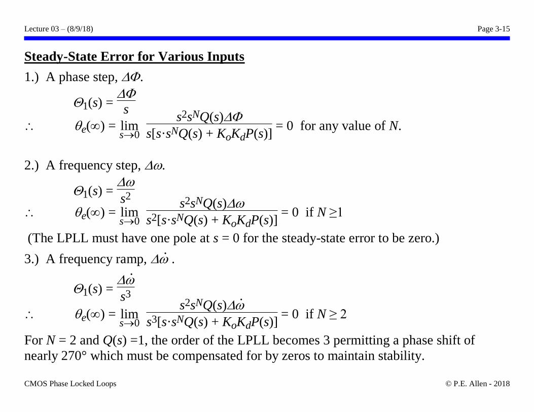
Steady-State Error for Various Inputs
1.) A phase step, .
1(s) = s
2.) A frequency step, .
1(s) =
s2
(The LPLL must have one pole at s = 0 for the steady-state error to be zero.)
3.) A frequency ramp, · .
1(s) = ·
s3
For N = 2 and Q(s) =1, the order of the LPLL becomes 3 permitting a phase shift of
nearly 270° which must be compensated for by zeros to maintain stability.
e() = lims→0
s2sNQ(s)
s[s·sNQ(s) + KoKdP(s)] = 0 for any value of N.
e() = lims→0
s2sNQ(s)
s2[s·sNQ(s) + KoKdP(s)] = 0 if N ≥1
e() = lims→0
s2sNQ(s) ·
s3[s·sNQ(s) + KoKdP(s)] = 0 if N ≥ 2
Lecture 03 – (8/9/18) Page 3-16
CMOS Phase Locked Loops © P.E. Allen - 2018
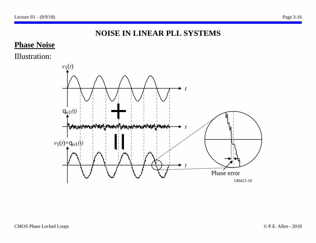
NOISE IN LINEAR PLL SYSTEMS
Phase Noise
Illustration:
v1(t)
t
t
qn1(t)
v1(t)+qn1(t)
t
Phase error140421-10

Lecture 03 – (8/9/18) Page 3-17
CMOS Phase Locked Loops © P.E. Allen - 2018
PLL for Noise Analysis
Assume that the input is band limited as shown below.
Bi = Bandwidth of the prefilter (or system)
Some terminology:
• Power spectral density is the measure of power in a given frequency range (Watts/Hz)
or (V2/Hz). It is found by dividing the rms power by the bandwidth.
• Consider all noise signals as white noise which means the power spectrum is flat.
• Ps = input signal rms power (V1(rms)2/Rin)
• Pn = rms power of the input noise
Phase
DetectorFilter
VCO
fof
Att
enu
atio
n (
dB
)
Bi
Prefilter
Input
Signal Output
140421-11

Lecture 03 – (8/9/18) Page 3-18
CMOS Phase Locked Loops © P.E. Allen - 2018
Power Spectra of a PLL
Illustration of how input noise
becomes phase noise in the
frequency spectrum:
Power spectra of the reference
signal, v1(t), and the superimposed
noise signal, vn(t).
Spectrum of the phase noise at the
input of the PLL.
Frequency response of the phase-
transfer function, H(j).
Spectrum of the phase noise at the
output of the PLL.
Sp
ectr
al P
ow
er
Den
sity
Frequency
Wi
BiArea = Pn
= WiBi
fo
Area = Ps
Frequency
qn1(jw)2
Bi/2
Area = vn12
F
FrequencyBL
Function of z
|H(jw)|
Frequency
qn2(jw)2
BL
Area = vn22
140421-12

Lecture 03 – (8/9/18) Page 3-19
CMOS Phase Locked Loops © P.E. Allen - 2018
Noise Relationships for a PLL
Spectral density of the input noise signal:
Wi = Pn
Bi (W/Hz)
Input rms phase noise jitter (or the square of the rms phase noise):
n1(t) → n1 2 = Pn
2Ps (Comes from the assumption of white noise)
Signal-to-Noise Ratio (SNR):
SNR at the input = (SNR)i Ps
Pn → n1 2 =
Pn
2Ps =
1
2(SNR)i (radians2)
Input phase jitter (noise) spectrum:
n1 2 (j) = = n1 2
Bi/2 (radians2/Hz)
Output phase jitter (noise) spectrum:
n2 2 (j) = |H(j)|2 n1 2 (j) = |H(j)|2
Lecture 03 – (8/9/18) Page 3-20
CMOS Phase Locked Loops © P.E. Allen - 2018
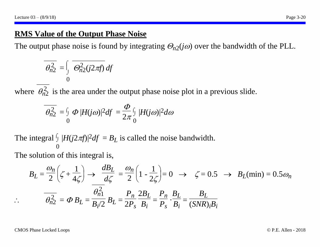
RMS Value of the Output Phase Noise
The output phase noise is found by integrating n2(j) over the bandwidth of the PLL.
n2 2 =
0
n2 2 (j2f) df
where n2 2 is the area under the output phase noise plot in a previous slide.
n2 2 =
0
|H(j)|2df =
2
0
|H(j)|2d
The integral
0
|H(j2f)|2df = BL is called the noise bandwidth.
The solution of this integral is,
BL = n
2
+ 1
4 →
dBL
d =
n
2
1 - 1
2 = 0 → = 0.5 → BL(min) = 0.5n
n2 2 = BL = n1 2
Bi/2 BL =
Pn
2Ps 2BL
Bi =
Pn
Ps ·
BL
Bi =
BL
(SNR)iBi

Lecture 03 – (8/9/18) Page 3-21
CMOS Phase Locked Loops © P.E. Allen - 2018
RMS Value of the Output Phase Noise – Continued
We noted previously that,
n1 2 = 1
2(SNR)i =
Pn
2Ps → (SNR)i =
Ps
Pn
A dual relationship holds for the output,
where (SNR)L is the signal-to-noise ratio at the output.
This equation suggests that the PLL improves the SNR of the input signal by a factor of Bi/2BL. Thus, the narrower the noise PLL bandwidth, BL, the greater the improvement.
Some experimental observations:
• For (SNR)L = 1, a lock-in process will not occur because the output phase noise is
excessive (0.707 radians or 40.4°).
• At an (SNR)L = 2, lock-in is eventually possible (0.5 radians or 28.6°).
• For (SNR)L = 4, stable operation is generally possible.
n2 2 = 1
2(SNR)L =
Pn
Ps ·
BL
Bi → (SNR)L =
Ps
Pn
Bi
2BL
(SNR)L = (SNR)i Bi
2BL
Note: (SNR)L = 4, n2 2 becomes 0.125 radians2. n2 2 = 0.353 radians 20° and the
limit of dynamic stability (180°) is rarely exceeded.

Lecture 03 – (8/9/18) Page 3-22
CMOS Phase Locked Loops © P.E. Allen - 2018
Summary of Noise Analysis of the LPLL
• Stable operation of the LPLL is possible if (SNR)L ≥ 4
• (SNR)L is calculated from
(SNR)L = Ps
Pn
Bi
2BL
where Ps = signal power at the reference input
Pn = noise power at the reference point
Bi = bandwidth of the system at the input
BL = noise bandwidth of the PLL
• The noise bandwidth, BL, is a function of n and . For = 0.7, BL = 0.53n
• The average time interval between two unlocking events gets longer as the (SNR)L
increases.

Lecture 03 – (8/9/18) Page 3-23
CMOS Phase Locked Loops © P.E. Allen - 2018
Pull-In Techniques for Noisy Signals
1.) The sweep technique.
When the noise bandwidth is made small, the SNR of the loop is sufficiently large to
provide stable operation. However, the lock range can become smaller than the
frequency interval within which the input signal is expected to be. The following
circuit solves this problem by providing a direct VCO sweep.
(1.) LPLL not locked.
(2.) RUN mode starts
a positive sweep.
(3.) When the VCO
frequency
approaches the
input frequency
the loop locks.
(4.) The “In-Lock”
detector switches
the sweep switch
to the “HOLD”
position.

Lecture 03 – (8/9/18) Page 3-24
CMOS Phase Locked Loops © P.E. Allen - 2018
Pull-In Techniques for Noisy Signals
2.) Switched filter technique.
In the unlocked state, the filter bandwidth is large so that lock range exceeds the
frequency range within which the input is expected.
In the locked state, the filter bandwidth is reduced in order to reduce the noise.
Phase
Detector
VCO
v2(t)
v1(t)Rsmall(not locked)
Rlarge(locked)
Switched Loop Filter
"In-Lock"
Detector
vf(t)
140421-14

Lecture 03 – (8/9/18) Page 3-25
CMOS Phase Locked Loops © P.E. Allen - 2018
SUMMARY
• Acquisition process – the PLL in the unlocked state
• Influence of noise on the linear PLL
• Pull-in techniques for noisy signals

![(Reference [2]) LINEAR PHASE LOCKED LOOPS - CONTINUED …pallen.ece.gatech.edu/Academic/ECE_6440/Summer_2003/L060-LPLL-II(2UP).pdf(Reference [2]) LINEAR PHASE LOCKED LOOPS - CONTINUED](https://img.dokumen.tips/doc/110x75/6016ce84e4e4bb557426a4e4/reference-2-linear-phase-locked-loops-continued-2uppdf-reference-2-linear.jpg)

![(Reference [2]) LINEAR PHASE LOCKED LOOPS - …users.ece.gatech.edu/.../ECE_6440/Summer_2003/L060-LPLL-II(2UP).pdf · (Reference [2]) LINEAR PHASE LOCKED LOOPS - CONTINUED THE ACQUISTION](https://img.dokumen.tips/doc/110x75/5ad972fe7f8b9a52528b89b2/reference-2-linear-phase-locked-loops-usersece-2uppdfreference-2.jpg)


![RF Module Design - [Chapter 8] Phase-Locked Loops](https://img.dokumen.tips/doc/110x75/55cebb77bb61eba32f8b45bd/rf-module-design-chapter-8-phase-locked-loops.jpg)


