Embed Size (px)
Citation preview


PDP-11 Mainframe Troubleshooting Guide
(Flows and DECAl OS)
COMPANY CON FIDENTIAL

1 st Printing. December 1976
Copyright e 1976 by Digital Equipment Corporation
The reproduction of this troubleshooting guide. in part or whole. is strictly prohibited. For copy information. contact the Educational Services Department, Digital Equipment Corporation. Maynard. Massachusetts 01754.

OECAIO
AC/OC .LO
BUS
CONSA
CONSB
HELP
INT OPT
LOADER
MAINDA
MAINDB
MEMA
MEMB
CONTENTS
Contents
Introduction
Troubleshooting Flow Diagrams
Location of AC LO and DC LO signals on CPU backplanes
Quiescent Unibus levels Location of signals on Unibus slot backplane pins
Quiescent console light displays
PDP-ll/05 console checkout procedure
What to do if all else fails
List of internal options including modules. location. required jumper and wire changes
For paper tape systems: procedures for loading and running the bootstrap and absolute loader and for loading the MAINDECs
For disk. DECtape. or magtape systems: procedures for using the hardware and software bootstrap loaders
List of available CPU. memory. and internal option MAINDECs
Acceptable times for running MAINDECs
Module utilization and jumper configuration and location for MMll-S. MFll-L(PI. and MFllU(P) memories. and SSYN delay adjustment procedure for parity memory
Strobe adjustment procedure for memories using the Gll0

DECAID
PROCA05
PROCA40
PROCA45
PROCB
PWRB-1
PWRB-2
PWRB-3
PWRB-4
PWRB-5
PWRB-6
PWRB-7
PWRB-8
PWRB-9
PWRO
REMOTE
START
CONTENTS (Cont)
Contents
GPR program. module utilization. SCl clock adjustment. proc. clock adjustment
Proc. clock adjustment. jumper location and con
figuration. module utilization
Module utilization. jumper location. and configuration
CPU modules that drive and receive Unibus
signals
PDP-11/40/45 CPU dc voltage checks
POP-11/40/45 regulator slot assignments
POP-11/40/45 crowbar problems
POP-11/40/45 distribution panel connectors
PO P-11 140/45 power harnesses and cables
POP-11/40/45 reguators' connectors
POP-11/40/45 procedure for removal of regu
lators. fuse location
POP-11/40/45 bulk supply connectors
PO P- 11 140/45 fuse location on and removal
procedure for bulk supply's power control board
POP-11/05/10 power connectors
Remote power control facility
Suggestions on what to do before actual hard
ware troubleshooting

THE PDP-11 MAINFRAME TROUBLESHOOTING GUIDE
INTRODUCTION
This guide is comprised of two major sections:
1. The Troubleshooting Flowchart 2. The DECAIDs.
It is intended that they be used concurrently by Field Service per
sonnel to aid them in locating and repairing faults in PDP-ll sys
tems that utilize PDP-ll/05/l 0/35/40/45 CPUs.
The guide makes two basic assumptions.
1. The Field Service technician has an excellent supply of
replacement parts (e.g .. modules. power regulators. cables. etc.).
2. There is a configured copy of DEC/Xll with the system
which has been loaded and run error-free at some time prior
to this failure. That is. the system has already been installed
and was fully operational at one time. The guide does not
provide the necessary information on how to install either
systems or add-ons to a system.
THE TROUBLESHOOTING FLOWCHART
The flows guide the Field Service technician through the steps he
must perform to isolate a fault to either a peripheral device or the mainframe and if it is found to be in the mainframe. then to either
the Unibus. power system. internal option. memory. or processor.
Once the fault has been isolated. the flows then indicate the steps to
follow to repair the fault on a field-replaceable-unit basis.

The symbology used in the flowchart is as follows:
o o D (---------)
Circle An entry from or exit to other pages of the flows with the pages listed in parentheses near the circle.
Diamond A decision point.
Rectangle A procedure or operation to be performed by the technician.
Bubble A reference to one of the DECAl Os that provides the technician with the information necessary to perform the operation or make the decision.
The 13 pages of flows are organized as follows:
1.-2. Starting and quick-check: loading and running system exercisers
3.-4. AC power
5.-6. DC power
7. Mainframes
8. Unibus
9.-10. Consoles
11. Processors
12. Memories
13. Peripherals.

The flowchart is intended to fulfill two primary functions.
1. To aid the technician in determining a logical troubleshooting approach to a system failure.
2. To help the technician develop an effective troubleshooting technique.
THE DECAIDS
The second section of the quide provides the troubleshooter with all the information necessary to perform the operations. do the adjustments, and make the decisions to isolate and repair a problem in a PDP-11 system. These DECAIDs cover all the detailed aspects of troubleshooting from how to load a diagnostic to the procedure for adjusting core memory strobes to locating the output pins on a power regulator's connector.
It is intended that these DECAl Os will be used by the technician on the job, providing information that is:
1. Much toO detailed to memorize
2. Hidden away in one of more than a dozen manuals and engineering drawings
3. Not available anywhere else.

NOTES:
TROUBLESHOOTING FLOWCHART
IF SOME OF THE FANS ARE TURNING aUT NOT 01M£R8 IN OTHER BOXES OR CABlN£TI. CHECK THE REMOTE POWER CONTROL FACILITY. SEE DECAID REMOTE.
REMEMBER TO CHECK THAT THE POWlR ON/OFF SWITCH IS NOT ON PANEL LOCK. TRY A FEW BASIC fUMCTIONS SUCH A8 LOAD ADDRESS, EXAMINE AND DEPOSIT INTO ALL BANKS OF MEMORY AND EXAMINE AND DEPOSIT INTO PERIPHERAL AND REGISTER ADDRESSES.

TROUBLESHOOTING FLOWCHART 2
1 WHEN RUNNING A MAINDEC IT IS SOMETIMES DIFFICUlTTO OETECTWHETHER IT IS RUNNING PROPERLY OR WHETHER IT tS HUNG IN A LOOP. READ THE MAINDEC'S WRITE.UP TO SEE IF YOU CAN USE SUCH TECHNIOUESAS SETTING UP THE SWITCH REGISTER TO CAUSE A FRIEQUENT PRINTOUT. EXERCISING THE CONSOlE TERMINAL'S "'UHTEA, RUNNING IN SINGLE ITERATION MODE. ETC.

TROUBLESHOOTING FLOWCHART 3
'"

TROUBLESHOOTING FLOWCHART 4
~==::::--,

1>,
TROUBLESHOOTING FLOWCHART 6
REPAIR OR AEPLACE
CABLE BETWEEN
DISTRIBUTION PANEl
AND BACKPLANE
~ .-.. "" .... ""'0"'" REPLACE
HARNESS BETWEEN
REGULATOR A.O
DISTR~BUT10N
PANEL
Befor. replacing ti1ehlse Or '-slutator_ eh...,.. 10. poliible cauI_ Fulty compo"."" within the r,guilltor i ••• II-cen c.u •• tha I .... 10 blow. Ch..,k for scor<:hing 01 the -,ell board 8"dlot componan1!o, Check the b.clcpl ..... to •• bent pin or. pl_ 01 wi •• which millht ba causing 8 ,hOI1 cir<:ult
II.V ...... I, an 1 '/010/10. check the YOlt8iJtll •• IIIIed In DECAID MRD

TROUBLESHOOTING FLOWCHART 6

TROUBLESHOOTING FLOWCHART 7
12,131
111 '"

TROUBLESHOOTING FLOWCHART 8
(1,51
NOTE REMEMBER. AC LO AND DCLOAREALSOPOWER SUPPLY DEPENDENT
REINSTALL MEMORY BANKS ONEATATIME UNTILTtleDNE GENERATING
THE8AD QUIESCENT
L~OE~::J.IS REPLACe
'"

TROUBLESHOOTING FLOWCHART 9
",II
,..,

___ TROUBLESHOOTING FLOWCHART 10 __ _
'"

___ TROUBLESHOOTING FLOWCHART 11
11.7,9.101

TROUBLESHOOTING FLOWCHART 12 __ _
11,11,121 '"

TROUBLESHOOTING FLOWCHART 13
12,7,'21
'"

DECAID AC/DC LO ______ _
LOCATION OF AC LO/DC LO SIGNALS
Signal 11/05 11/40" 11/45"
M726l M7235 M8l06 ACLO B08Fl B0602 C12Sl DC LO B08F2 B06Cl C12Ul
(Very difficult to scope. Check on tab connector)
Quiescent levels should be +4.8 V ± 0.2 V
AC LO and DC LO are generated in the above CP modules. the bulk power supplies. and the power supplies of all peripherals. These are all connected to the Unibus in a wired OR. The processor receives them and makes itself and its memories totally inoperative if either one is true. It. therefore. will be necessary to physically disconnect the system in a logical fashion to determine which device is faulty .
• The following displays will be seen on the front penel if DC LO is true:
PDP·t 1/45 - The CPU's microaddress will be 200.
PDp·ll/40 - The CONS and AUN lights will ba off and the BUS and PAOC lights will ba on.

OECAIO BUS
QUIESCENT UNIBUS LEVELS
Normal bus quiescent levels are listed below. Anv level that deviates from
normal should be looked upon as a potential failure. In most cases. this improper level will be caused bV a defective bus receiver or driver. AC LO and
DC LO are also power-supplV dependent.
Signal
BG(7:4). NPG. BBSY (on PDP-1 1/40)
ACLO. DC LO
All others
Procedure
To measure quiescent Unibus levels:
Quiescent Level
+0.4V ± 0.4V
+4.8 V ± 0.2 V
+3.4 V ± 0.2 V
1. Turn the svstem on with the processor halted. Press the START kev and release it with HALT down. (On older PDP-1 1/40s it is neces
sary to LOAD ADRS 000000 to clear the A<17:00> lines.)
2. Use a calibrated oscilloscope to measure the Unibus signal lines.
(See the following chart of Unibus slot backplane pins.)
To obtain meaningful readings of bus grant lines (BG<7:4> and NPG). thev
should be measured at each device wired to them down the length of the bus.
All buses should be checked in multiple bus svstems.

________ OECAIO BUS
UNIBUS SLOT (Viewed from the Backplane)
INIT
I~~~ ---t-:O-i. D02--+'~. DO' D06--+=---_ DO. Dl0--+,~. 012
DDll~'==~.! PA-
NPG:===~~9 B.7
BG:~-====~~~ BG. BA,
AC LO ----,A.,.O,..., ---t-:O-i1) A03 ---t-:~. A06 A07 ---t-:~. AO. All ---t-:~. A13 A16 ---t-:O-i. A17
SSVN :===l~'" MSVN
OGND
• +3.4±.2V
ED +.4V±.4V
o +4.IV±.2Y>
+6V
-.. ~+==DOl • 003 00'
~07 DO.
011 013 016
P. BBSV(+.4V±.4V ON 11/401 SACK
:~~==NP . • A7 B."
+6V
:~~~~~~~B:A' BG' DCLD ADO A02
.-7-+--AD4 A08 .-=-+---AD9 Al0
.-=-+--:~!
~~Al.
o Cl CO

DECAID CONSA
QUIESCENT CONSOLE LIGHT DISPLAY
Press and release the START key with the HALT key down.
PDP-11/40 ADRS = 000000
DATA = 000000
RUN = ON
BUS = ON PROC = ON
CONSOLE = ON
All the rest = OFF
PDP-11/46 All ADRS = 000000 DISPLAY REG = 000000
BUS REG = 000000 DATA PATHS = Contents of RO
I'ADRS CPU = 170 (200 when START is held down)
KERNEL = ON (OFF when START is held down)
MASTER = ON All the rest = OFF

DECAID CONSB
PDP·11106 CONSOLE CHECKOUT PROCEDURE
1. Make certain the computer power is off.
2. Disconnect the console cable connector from the M7260 module and
then turn on the computer power.
3. Aher step 2 is completed. the data pattern 177777, should be displayed on the console lights.
4. At the connector that plugs into the M7260 module. use a piece of small gauge wire and jumper pin F to the following pins and observe if the
displayed pattern is correct. Remove the jumper each time before pro·
ceeding to the next step.
5. Jumper: GND; Pattern: 000000
6. Jumper: N; Pattern: 125252
7. Jumper: L; Pattern: 146314
8. Jumper: J; Pattern: 170360
9. Jumper: 0; Pattern: 177400
10. Remove the jumper aher completing the procedure.

________ DECAtO HELP _______ _
WHAT TO DO WHEN ALL ELSE FAILS
Most of the cases in the flowchart that take you here are for problem symp
toms that are very unusual. Make sure you have checked every possibility. If
you have a solid problem and you just don't know where to go, start at NO-OP
on flow page 1.

OECAIO INT OPT
PROCESSOR'S INTERNAL OPTIONS
PDP-ll/06
None
PDP-11/40
KEll-E
KEll-F
KT11-0
KJll-A
KW11-L
PDP-11/46
FPll
KT11-C
KW11-L
Extended I nstruction Set M7238, slot 2
Requires jumper changes; see DECAID PROCA40
Floating Instruction Set M7239. slot 1 Requires jumper changes; see OECAIO PROCA40
Memory Management M 7236. slot B Requires jumper changes; see OECAIO PROCA40
Stack Limit Register M7237. slot 3E Requires jumper changes; see OECAIO PROCA40
Line Clock M7B7. slot 3F Requires wire change; see OECAIO PROCA40
Floating Point Processor MBl14. slot 2 MB115. slot 3 MB112. slot 4 MB113. slot 5 No jumper changes required.
Memory Management MB10B. slot 13 MB107. slot 14 Requires removal of MB 116 from slot 14
Line Clock M7B7. slot lC Requires removal of wire between pin COl R2 and pin C01V2.

_______ DECAID LOADER
FOR SYSTEMS EQUIPPED WITH PAPER TAPE
NOTE In the followinll de.cription., the value XX reflacta the system's memory .iza a •• hown below:
Mamory Size XX
4K 01 8K 03
12K 06 18K 07 20K 11 24K 13 28K or IIreatar 16
LOAD ADRS ............................................................................................ XX7744 DEPOSIT .................................................................................................. 016701
000026 012702 000352 005211 105711 100376 116162
000002 XX7400 005267 177756 000765
177560 (nY)
or 177550 (PC11)

DECAID LOADER
Place the Absolute Loader tape in the specified reader with the special boot
strap leader code (ASCII code 3 5t) over the reader sensors.
LOAD AORS ............................................................................................ XX7744
START
The Absolute Loader tape will pass through the reader and will stop when the last frame of data has been loaded into memory.
Place the MAIN DEC tape in the specified reader with blank leader tape over
the reader sensors.
Press CONT or
LOAOAORS ............................................................................................ XX75OO
START
The MAINOEC tape will pass through the reader and will stop when com
pletely loaded into memory.
At this time RO which is displayed in the DATA display· will contain all zeros
in the low byte. If not. a checksum error has occurred indicating that some data was incorrectly loaded. The tape should be reloaded.
FOR SYSTEMS EQUIPPED WITH DISK. DECtape. AND/OR MAGTAPE
Hardware Bootstrap Loaders
The following table describes the procedures for loading the MAl NDEC monitors. Ensure that your XXDP medium is on drive O .
• For PDP-tt/05: to read RO. load address t77700 and press EXAM switch.

_______ DECAID LOADER
ROM Device Proceduure
BM792-YB RK11/RK05 LOADADRS ............... 773100 SWITCH REG .............. 777406 START
TC11ITU56 LOAD ADRS ......... ".".773100 SWITCH REG ............. 777344 START
MR11-DB RKll/RK05 LOAD ADRS ............... 773110 START
TCllITU56 LOAD ADRS ............... 773120 START
TMll/TU10 LOAD ADRS ............... 773136 START
RPll/RP03 LOAD ADRS ............... 773154 START
BM873-YA RKll/RK05 LOAD ADRS ............... 77301O START
TCllITU56 LOAD ADRS ............... 773030 START
TMllITU10 LOAD ADRS ....... , ....... 773050 START
TA11/TU60 LOAD ADRS ............... 773230 START
RPll/RP03 LOADADRS ............... 773100 START

_____________ DECAIDLOADER
ROM Device Procedure
BM873-YB RKll/RK05 LOAD ADRS ............... 773030 (unit zero) START
RKll/RK05 LOAD ADRS ............... 773032 (Unit specified START in Switch register)
TCllITU56 LOAD ADRS ............... 773070 START
TMllITU10 LOAD ADRS ............... 773110 START
TJU16ITU16 LOAD ADRS ............... 773150 START
TA11ITU60 LOAD ADRS ............... 773524 START
RP11/RP03 LOAD ADRS ............... 773350 START
RJPQ4/RP04 LOAD ADRS ............... 773350 START
RJS03/RS03 LOAD ADRS ............... 773000 START

DECAID LOADER
Software Bootstrap Loaders
If the hardware bootstrap doesn't work, try one of the following software bootstraps depending on your particular syystem configuration.
Device
RK11/RK05
TC11ITU56
Procedure
LOADADRS ... DEPOSIT ...................... .
..010000
.. 012737
000005 177404
000001 LOAD ADRS ........................... 010000 START Wait 1 second. LOAD ADRS ............................ 000000 START
LOAD ADRS ............................. 777342 DEPOSIT ................................... 004003 DECtape will rewind. EXAMINE DEPOSIT ................................... 000001 LOAD ADRS ............................. 000216 DEPOSIT .................................. 012737
000005 177342 000777
LOAD A DRS ............................. 000216 START

_______ DECAID LOADER ______ _
Device
TMll/TU10
Procedure
LOAD ADRS.... .. .. 010000 DEPOSIT.. ............................... 005137
172524 012737 060011 172522 000777 012737
060003 172522 000777
LOAD A DRS ............................ 010000 START Wait 1 second. Press HALT switch. LOAD A DRS ............................ 010014
START Wait 1 second. Press HALT switch.
LOAD ADRS ........ START
.. ...... 000000

_____________ DECAIDLOADER
Device
TJU16ITU16
Procedure
LOAD ADRS ............................. 010oo0 DEPOSIT ................................... 012737
001300 172472 012737 177777 172446 012737 000031 172440 105737 172452 100375 012737 177400 172442 005037 172444 042737 000007 172452 012737 000071 172440 105737 172440 000100 000375 000137 000000
LOAD AD RS ............................. O 10000 START

______________ DECAIDLOADER
Device
TA11ITU60
Procedure
LOAD ADRS ............................. 001 000 DEPOSIT ................................... 012700
177500 005010 010701 062701 000052 012702 000375 112103 112110 100413 130310 001776 105202 100772 116012 000002 120337 000000 001767 000000 000755 005710 100774 005007 017640 002415 112024
LOAD ADRS ....................... , ..... 001 000 START

_______ DECAID LOADER ______ _
Device
RX11/RX01
RP11/RP03
Procedure
LOAD ADRS ............................. 001 000 DEPOSIT ................................... 005000
012701 177170 105711 001776 012711 000003 005711 001776 100405 105711 100004 116120 000002 000770 000000 005000 000110 000000 000000 000000
LOAD ADRS ............................. 001 000 START
LOAD ADRS ............................. 001 000 DEPOSIT ................................... 012705
176716 012715 177400 012745 000005 105715 100376 005007
LOAD ADRS ............................. 001000 START

_____________ OECAIOLOADER ____________ _
Device
RJP04/RP04
RJS04/RS04 RJS03/RS03
Procedure
LOAD ADRS ............................. Ol0000 DEPOSIT ................................... 012700
176700 012710 000023 005060 000034 005060 000006 012760 177400 000002 012710 000071 105710 100316 005007
LOAD ADRS ............................. Ol 0000 START
LOAD ADRS ............................. OOI 000 DEPOSIT ................................... 012705
172044 012745 177400 012745 000071 032715 100200 001775 100762 005007
LOADADRS ............................. 001000 START

_______ DECAIDMAINDA ______ _
MAIN DEC NAMING CONVENTION
o C FP KA-X -I MCN level
x = No MCN ever issued
o = Initial MCN announcing latest program version
1-9 latest MCN revision level
A thru Z = revision designation
A thru Z = program designation o thru 9 = overlay designation
2 digits = option designation
~ A = 11/05. 15. 20 processors . B = 11/40 processor C = 11/45 processor D = 11/05 only E = 11170 system Z = all processors
" X = DEC/X 11 exerciser software
D indicates a Diagnostic Program. and is not used in naming a program.

DECAID MAINDA
MAINFRAME MAINDECS AND THE PROCESSORS THEY Run On
Name Number 05 40 45
CTP Communications DZOCA X X X
GTPGeneral DZOGA X X X
T17 4K. CPU. 1/0 DZOKB X X X 11 Family Instruction Exerciser DZOKC X X X 11/40 and 11/45 DCOKC X X,
Instruction Exerciser
Multiplication-Division DCOKA EIS X Exerciser 11/40 and 11/45 Processor DCKBR PAR PAR
Parity
11/45 Console Test DCKBO X
States 11 145 DCKBO X PIRO DCKBN X Traps 11/45 DCKBM X T14 11 lOS. 20 Traps DONC X T14 11140 Traps DBKDM - X Power Fail 1'1/45 DCKBP X Power Fail 11/05.20.40 DZKAO X X
DIV DCKBL EIS X MUL DCKBK EIS X ASHC DCKBJ EIS X ASH DCKBI EIS X 11/45 Registers DCKBH X SPL DCKBG X Stack Limit DCKBF KJ X RTT DCKBE X X MARK DCKBD X X XOR DCKBC X X
SOB DCKBB X X
SXT DCKBA X X

_______ DECAIDMAINDA ______ _
BASIC MAINFRAME MAINDECs (Run On All Processors)
Name Number
T1 3 JSR. RTS. RTI DOMA T12Jump DOLA Tll Subtract DOKA Tl0 Add DOJA T9 Bit Set Clear Test DOIA T8 Move DOHA T7 CMP Non-Equality DOGA T6 CMP Equality DOFA T5 Rotate/Shift DOEA T4 Binary DODA T3 Unary DOCA T2 Con Branch DOBA Tl Branch DOAA

DECAID MAINDA
MEMORY MAINDECS AND THE PROCESSORS THEY RUN ON
Name Number 05 40 45
0-124K Memory Exerciser DZQMB X X X
Memory 1/0 Exerciser DZQMA X X X
Up-Down Address Test DZMMK X X X
BK Special DZMMJ X X X
Random Data DZMMI X X X
Core Heating DZMMH X X X
Worst Case Noise DZMMG X X X
Ones Susceptibility DZMMF X X X
Moving Ones and Zeros DZMME X X X
Basic Test Patterns DZMMD X X X
No Dual Address Test DZMMC X X X
Basic Address Test Down D1BA X X X
Basic Address Test Up D1AA X X X
MAll,MFll, and MSll DCMFA PAR PAR
Parity Test
MSll DCMSB MOS
BIP

_______ OECAIO MAINOA ______ _
INTERNAL OPTION MAINOECS
POP-11/45 Floating Point - FP11
Name
GTP Overlay Basic Instruction Exerciser
Division Exerciser Multiplication Exerciser
Addition and Subtraction Exerciser LD D/STD Exerciser
Maintenance MODF. MODD
LDEXP. STEXP
LDCJX. STCXJ
LDCDF.LDCFD.STCDF.STCFD
CLR. TST. ABS. NEG DIVF. DIVD MULF. MULD CMPF.CMPD
ADDF. ADDD. SUBF. SUBD
LDF. LDD. STF. STD
STS. Illegal Instructions
Basic Test
Number
DCOOA DCFPO
DCFPU DCFPT
DCFPS
DCFPR
DCFPM DCFPL
DCFPK
DCFPJ
DCFPI
DCFPH
DCFPG DCFPF
DCFPE
DCFPD DCFPC
DCFPB
DCFPA
PO P-11 /45 Memory Management - KT11-C
Name Number
Exerciser DCKTG Abort DCKTF
MFPD/I DCKTE
MTPD/I DCKTD
Keys DCKTC
Logic 2 DCKTB Logic 1 DCKTA

_______ OECAIO MAINOA ______ _
POP-11!40 Floating Point - KE11-F
Name
GTP Overlay
Exerciser Basic Instruction Test
Number
OBKEO
DBKEB
DBKEA
POP-11!40Memory Management- KT11-0
Name
Exerciser Abort
States MFPI/MTPI
Keys
Logic
Line Clock - KW11-L
Name
Exerciser
Number
DBKTG
DBKTF DBKTD
DBKTC
DBKTB
DBKTA
Number
DZKWA

DECAID MAINDB ______ _
PDP-" SYSTEMS TESTS
1. DEC/Xll
2. DZQGA
DZQCA
2 hours or 2 passes
GTP (for non-commu- 2 h 0 u rs 0 r 2 nication-oriented systems)' or
passes
CTP (for commu- 2 hours or 2
nication-oriented sys- passes tems)'
, Mechanical devices. e.g .. TTY. line printers. should onlv be run 5 minutes.
PDP-11/05/10 CUSTOMER ACCEPTANCE DIAGNOSTICS
Central Processor
1. DZQKC 11 Family Instruction 30 minutes Exerciser. any switch
0-7 up
2. DONC T14 11/05. 20 traps 2 passes
3. DZQKB T17 Systems Test. only 10 minutes console device enabled
4. DZKAQ Power Fail .10 power fails
Read/Write Memories
1. DZQMB
2. DZQMB
3. DZMMI
0-124K Memory Exerci
ser. with switch 11 u.11 1 minute/8K
0-124K Memory Exerci- 2 minutesl8K ser. 8K or greater
Random Data. for less 5 minutes than 8K only

_______ DECAID MAINDB
PDP-11/35/40 CUSTOMER ACCEPTANCE DIAGNOSTICS
Central Processor
1. DCQKC
2. DBKDM
3. DZQKB
4. DZKAQ
11/40 and 11/45 Instruction Exerciser. any switch 0-7 up
30 minutes
T14 11/40 Traps 2 passes
T17 Systems Test. only 10 minutes console device enabled
Power Fail 10 power fails
Read/Write Memories
1. DZQMB 0-124K Memory Exerci- 1 minute/8K ser. with switch 11 up
2. DZQMB 0-124K Memory Exerci- 2 minutes/8K ser. 8K or greater
3. DCMFA Parity Test 2 passes
Stack Limit Option - KJ11-A
1. DCKBF Stack Limit Option Test 2 minutes
Extended Instruction Set - KE11-E
1. DCKBI- ASH. ASHC. MUL. DIV 2 minutes each DCKBL Test
2. DCQKA MUL. DIV Random 20 minutes Exerciser

_______ DECAID MAINDB
Floating Instruction Set - KEll-F
1. DBKEB KE11-F Exerciser 20 minutes
2. DBKEO GTP Overlay 20 minutes
Memory Management - KT1l-D
DBKTG KT11-D Exerciser 4 minutes/8K
PDP-ll/45/50 CUSTOMER ACCEPTANCE DIAGNOSTICS
Central Processor
DCOKC
2. DZOKB
3. DCKBP
11/40 and 11/45
Instruction Exerciser
T17 Systems Test. only
console device enabled
Power Fail
30 minutes
10 minutes
1 pass
Read/Write Memories
1. DZOMB
2. DZOMB
3. DCMFA
4. DCMSB
0-124K Memory Exerci
ser, with switch 11 up
0-124K Memory Exerci
ser, 8K or greater
Parity Test
MOS Memory Test
1 minute/8K
2 minutes/8K
2 passes
2 passes
Floating Point Processor - FPll
1. DZFPO FP11 Exerciser 20 minutes
2. DCOOA GTP Overlay, all avail- 20 minutes
able devices enabled
except line printer if any

OECAIO MAINOB ______ _
Memory Management - KT11-C
1. OCKTG KT11-C Exerciser. all
available devices
enabled except line
printer if any
1 pass

DECAIDMEMA
MM11-S MODULE UTILIZATION
A
-I---
-
-
-
. N ~
-
o
C;

\: DECAID MEMA II~~ ______ _
MF11-L(PI MODULE UTILIZATION ~ ~;.. ~t , \;
• I·
A
-
-f-- -
~ - N " ~
~ ~ ~
" ~
N ~
- ~
-
* IF PARITY MEMORY.
-

DECAIDMEMA
G110 CONTROL MODULE JUMPERS
See the next page for a diagram showing the physical location of
the jumpers.
Device Address Jumpers'
Memory Machine W6
Bank Address A14 or W4 W3 W2 (words) (words) A01t A15 A16 A11L
0-8K 000000-037776 In In In In
8-16K 040000-077776 Out In In In 16-24K 100000-137776 In Out In In
24-32K 140000-177776 Out Out In In
32-40K 200000-237776 In In Out In 40-48K 240000-277776 Out In Out In 48-56K 300000-337776 In Out Out In
56-64K 340000-377776 Out Out Out In
64-12K 400000-437776 In In In Out 12-80K 440000-477 77 6 Out In In Out
80-88K 500000-537776 In Out In Out 88-96K 540000-577776 Out Out In Out 96-104K 600000-637776 In In Out Out
104-112K 640000-677776 Out In Out Out 112-120K 700000-737776 In Out Out Out 120-128K 740000-777776 Out Out Out Out
• W5 and W10 must be installed and W9 must be removed (for BK stacks).
t The memory can be interleaved as 16K only, using two adjacent con
tiguously addressed BK banks. When two BK banks are interleaved, jumpers
W7 and WB must be in the configuration shown by the dotted lines. Bit A01
goes to the device selector gate controlled by jumper W6. One B K bank
must have W6 installed and the other must have W6 removed.
When not interleaved. jumpers W7 and W8 must be in the configuration
shown by the solid lines. Bit A 14 goes to the device selector gate controlled
by jumper W6.
W7
6--n WB
~ Non-Interleaved
0- W7~.Q ' ....... /",
" "-" "/ WB ' d '0
Interleaved

CONTROL MODULE G110
COMPONENT 510E SHOWING PHYSICAL LOCATION Of JUMPERS
NOTES: 1. Jumper WI is for fest purposes only. It must be Installed for normal operation. 2. Jumper WI' should be removed for normal operation.When installed the memory
responds 10 DATI onlY,regordless of slate of control lines COO and COL 3. Jumpers W70nd we must remain in the factory installed positions. 4. When used as on 8k bonk, jumpers W5 and WIQ must be Instolled ond jumper
W9 must betemoved. 5. When used as a 4k bonk,jumperWl0must. be removed and jumper W9mus' be
installed. Jumper W5 determines the locollonof the bonk on the bus.
C)
0 (") 0 Z -I :JI 0 ... 3: 0 c c: c ... m m (")
~ C 3: m 3: »
V CONNECTOR EDGE /

DECAID MEMA
MF11-U(PI MODULE UTILIZATION
~ 5 ~ ~ 0
- ~ ~ . iii ~ ; ,
iii ,
I---
~ .. ! I ~ ..
- ;;; ~ c; ,j
~ I - i
-
* IF PARITY MEMORY.

DECAIDMEMA
M8293 DEVICE ADDRESS JUMPERS
Memory Machine Bank Address W7 W6 W5 W4 W3
(Words) (Words). A17 A16 A15 A14 A13
0-16K 000000-077776 IN IN IN IN IN 4-20K 020000-117776 IN IN IN IN OUT
8-24K 040000-137776 IN IN IN OUT IN 12-2SK 060000-157776 IN IN IN OUT OUT
16-32K 1 00000-1 7777 6 IN IN OUT IN IN 20-36K 120000-217776 IN IN OUT IN OUT
24-40K 140000-237776 IN IN OUT OUT IN 2S-44K 160000-257776 IN IN OUT OUT OUT 32-4SK 200000-277776 IN OUT IN IN IN 36-52K 220000-317776 IN OUT IN IN OUT
40-56K 240000-337776 IN OUT IN OUT IN 44-60K 260000-357776 IN OUT IN OUT OUT
4S-64K 300000-377776 IN OUT OUT IN IN 52-6SK 320000-417776 IN OUT OUT IN OUT 56-72K 340000-437776 IN OUT OUT OUT IN 60-76K 360000-457776 IN OUT OUT OUT OUT
64-S0K 400000-477776 OUT IN IN IN IN 6S-S4K 420000-517776 OUT IN IN IN OUT 72-SSK 440000-537776 OUT IN IN OUT IN 76-92K 460000-557776 OUT IN IN OUT OUT SO-96K 500000-577776 OUT IN OUT IN IN S4-100K 520000-617776 OUT IN OUT IN OUT
SS-104K 540000-637776 OUT IN OUT OUT IN 92-10SK 560000-657776 OUT IN OUT OUT OUT
96-112K 600000-677776 OUT OUT IN IN IN 100-116K 620000-717776 OUT OUT IN IN OUT 104-120K 640000-737776 OUT OUT IN OUT IN 10S-124K 660000-757776 OUT OUT IN OUT OUT
112-124K 700000-757776 OUT OUT OUT IN IN 116-124K 720000-757776 OUT OUT OUT IN OUT 120-124K 740000-757776 OUT OUT OUT OUT IN
NOTE: The memory maybe interleaved in 32K increments. using two contiguously addressed 16K banks.

DECAIDMEMA
In the 16K interleaved memory configuration the following changes
must be made:
WI is cut.
W2 is in. W8 is in. W9 is in. } Wl0 is cut.
For one 16K of the interleaved pair
W9 is cut. } Wl0 is in. For the other 16K of the interleaved pair
Both interleaved memories should be cut for the same starting
address.
Non-Interleaved
WI is in. W2, W8, W9, and WI 0 are cut.

____ DECAIDMEMA ___ _
M8293 16K UNIBUS TIMING MODULE
W3,W5.
NOTE:
W1. W2, we, W9, AND W10ARE SELECTED FOR INTERLEAVED OR NON-INTERLEAVED OPERATION. W3, W4. W5. W6.ANO W7 ARE SelECTED FOR STARTING ADDRESS

DECAIDMEMA
PCl SSYN DlY l ADJUSTMENT PROCEDURE FOR M7269 PARITY CONTROllER
This adjustment sets a 1 05-ns delay from the leading edge of SSYN
INT BUS L to allow sufficient settling time for the parity checking logic. Too long a delay will result in increased cycle time and access
time. The waveshapes should be as shown below. Adjust R 16 to
obtain the required delay.
SSYN DlY l TIMING RELATIONSHIP

DECAIDMEMA
CSR ADDRESS JUMPER SELECTION FOR M7269 PARITY CONTROLLER MODULE. Etch Rev D. CS Rev E
CSRJumpers W4 W3 W2 W1
Bus Address Line A04 A03 A02 A01
Lower Memory
Boundary CSR Address
OK 772100 X X X X 4K 772102 X X X 0 8K 772102 X X X 0
12K 772104 X X 0 X 16K 772104 X X 0 X 20K 772106 X X 0 0 24K 772106 X X 0 0 28K 772110 X 0 X 0 32K 772110 X 0 X X 36K 772112 X 0 X 0 40K 772112 X 0 X 0 44K 772114 X 0 0 X 48K 772114 X 0 0 X 52K 772116 X 0 0 0 56K 772116 X 0 0 0 60K 772120 0 X X X 64K 772120 0 X X X 68K 772122 0 X X 0 72K 772122 0 X X 0 76K 772124 0 X 0 X 80K 772124 0 X 0 X 84K 772126 0 X 0 0
(Continued)

DECAIDMEMA
CSRJumpers
Bus Address Line
Lower Memory
Boundary CSR Address
88K 772126 92K 772130
96K 772130
lOOK 772132
104K 772132 108K 772134
112K 772134
116K 772136
120K 772136
o = Jumper Removed X = Jumper Installed
W4
A04
0 0 0 0 0 0 0 0 0
W3
A03
X 0 0 0 0 0 0 0 0
W6: Removed for MF11-LP. installed for MF11-UP
W2 W1
A02 A01
0 0 X X X X X 0 X 0 0 X 0 X 0 0 0 0

PARITY ERROR INDICATOR
co I W3 [SABCDEFHJKL 0 \ e
w7ID~Dlw4Dlw2DoD D D 00 <;> Q: <;> 1 <;> <;> <;> gg I\D o 0 0,0 0 0 DQ,§@
··1 0 a I-a I a a 0 1 0 I ~ ©
o 0 0 0 0 I DO! OI~Q JUMPERSCONTROLO~TIONSA~LOWS' 0 0 0 0 0 ~ @
R16 Wl-W4 SELECT CSR ADDRESS W5 CAPACITOR FOR SSYN DELAY (NEVER USEDI W6 OUT FOR MF11-lP,IN FOR MF11-UP W7 OUT TO HANG BUS ON PARITY ERROR
SSYN DELAY ADJUSTMENT
inS: .. -.I n N ~UI ::aU) CD "lI ~ » C::a -::::j
< 0 0 Z -t ::a C 0 m r- 0 s: !: .c C C s: c: m r- s: m
»

DECAIDMEMB
STROBE ADJUSTMENT PROCEDURE FOR MEMORIES USING THE G110
When any module in the memory system is replaced. the strobe must be adjusted for that system.
To adjust the strobe. use DZQM BC or a higher revision of the 0-124K Memory Exerciser MAINDEC.
Start the diagnostic at AD RS 214. allowing you to enter test parameters. Cycle on the bank to be adjusted while running pattern 1. Check program procedures for further information.
Attach and sync channell to READ H pin CU2 of the G110 and channel 2 to STROBE H at test point 1 on the G110. (See the next page for the location of TP 1.)
Adjust the strobe to the earliest (minimum) setting at which the memory will cycle error free and allow the test to run for three minutes.
Adjust the strobe to the latest (maximum) setting at which the memory will cycle error free; this adjustment is most critical and there should not be more than 5 ns difference between the failing and passing points on this adjustment. Allow the test to run at this setting for three minutes or more.
This window should be 50 ns minimum. If it is not. replace modules within that bank of memory until it is.
Adjust STROBE H to be 25 ns (leading edge to leading edge) from the latest (maximum) setting.
READ H I i PIN CU2 ---l I 5 ... mIn :-=j L-ON GUO
1---- 2 ...
STROBEH r-l_ .. _ rI_.. r-' TP10NG110----.J ~ ~! ..:u="':::..' __

DECAIDMEMB
G110 CONTROL MODULE
STROBe ADJUSTMENT R1Z0
HI r---"------:'::~:-::o...c-\= 1~~1,---_-----,18 8 I CJD CJCJ
I CJCJCJc::::::J ~TP'

_______ DECAID PROCA06 ______ _
PDP-11/06 MAINTENANCE
The PDP-11 /05 has the ability to run a program in its General Purpose registers. Therefore. disconnect all Unibus devices and all memory from the processor and if the console switches operate properly. attempt the program shown below.
General Purpose Register (GPR) Program
LOAD ADRS ........................................................................... 177700 DEPOSIT ...... ................... . .................................... 000240
000777 LOAD ADRS .......................................................................... 177700 START The program is now being executed.
The run light should come on. Press the HALT switch. The ADDRESS/DATA display should contain either 177700 or 177701.
If a processor problem is indicated. replace the M7260 and M7261 modules. and attempt the failing procedure after each replacement.
Always replace one module at a time to ensure that you don't plug a module into the wrong slot. If you are not absolutely positive. check the module utilization diagrams in this DECAID.
After replacing the M7260. it may be necessary to adjust the SCL clock as shown in this DECAID.
Remember. When you replace the M7261 module. check and if necessary. adjust the processor's clock rate as outlined in this DECAID.

_______ DECAID PROCA05 ______ _
PDP-11/05-JA MODULE UTILIZATION (16K)
UNIBUS TERMINATOR M930 OR EXTERNAL UNIBUS CABLE
PERIPHERAL CONTROLLER GRANT CONTINUITY CARD G127 {SLOT Oil
MEMORY STACK H213(4K) OR (8K)
3 I MEMORY DRIVER G231
4 I MEMORY CONTROL GUO
5 I UNIBUS TERMINATOR "'930 II MEMORY STACK H213 14K) OR (8K)
6 ) MEMORY DRIVER G231
7 I MEMORY CONTROL GilD
8 I KDl1-S PROCESSOR M7261
9 f 1(011-8 PROCESSOR M7260
I CONNECTOR
PDP-11/05-LA MODULE UTILIZATION (SK)
OFtI COMMUNICATIONS LINE ADAPTER
PERIPHERAL CONTROLLER OR GRANT CONTINUITY CARD G727 (SLOT 01)
I KMlI II I<Mll PERIPHERAL CONTROLLER
2 ~=:::MA="=T=:~::::=M:::"=NT=~ ~====:::O:::':::G:::":::NT=CO:::N:::":::NU:::IT=Y:::CA:::':::D:::":::2=' ::!S::LO::T::D::21==~ UNIBUS TERMINATOR M930 OR EXTERNAL UNIBUS CABLE
4 I BLANK
5 I UNIBUS TERMINATOR M930
PERIPHERAL CONTROLLER OR GRANT CONTINUITY CARD G727 (SLOT 03)
PERIPHERAL CONTROLLER OR GRANT CONTINUITY CARD G127 (SLOT 04)
MEMORY STACK H213 (410 OR H214 (810
6 ~1===========ME=M=O'=Y=D="=VE='=G=21=3===========~ ,I ~===========M=E=MO='=Y=CO=N=T'=O=L="=W===========~ '~I==========='="='-='=P='O=~=S=SO='=M=72=6='====================~ ,1 L ________ ~------~---'-D1-'--B-P-RO~CE-S-SO-'-.-72-6-0--~------~--------J I

... 'V
~ C ... ~ ~ ... "-
H213 14K) O~ H214 18K} MEMORY STACK II M930 UNIBUS I'" ::I C TERMINATOR n UI
:1"
G231 MEMORY DR I VER I'" 3: 2 o 3: c 0
I .. ::I C Gl to MEMORY CONTROL ~. ::I c:
a::I r- C 6231 MEMORY DRIVER I", 111 m m
o c: n
~¢ I'" .!!.::! ~
Gll0 MEMORY CONTROL r- C N 'V
H213 (4K) OR H214 18K) MEMORY STACK
" M930 UNIBUS I"
)0 :II TERMINATOR ..... 0
!:. 0 n ~
M7261 KDtl-B PROCESSOR CONTROL LOGIC a MICROPROGRAM 2 )0
~ c CJI
~ M7260 KD11-B PROCESSOR DATA PATHS IN KMII-B II KM11-A I I M9970 CABLE I OFII COMMUNICATIONS MAINT MAINT CONNECTOR LINE ADAPTER
I '" 1 0 (')
1 '" "

MS293 MEMORY CONTROL MODULE
G1I4 SENSE/INHIBIT MODULE
H217-D MEMORY STACK MODULE
G23$ X-V DRIVE MODULE
SPC SLOT i<
SPC SLOT*
SPC SLOT*
I0Il7261 CPU CONTROL MODULE
M7260 CPU DATA PATHS MODULE
.930 UNIBUS TERMINATOR*'"
M9970 OR M997
CONNECTOR MODULE
M930 UNIBUS TERMINATOR
.... "V
~ C
...... ~ ~ ....
...... ::I 0 n UI ;:r ~ s:: 0 0 u. C ::I s:: .. E' 0
'" C C DI c: m 0 r- (')
~ m ~ c: c ~ "V r- 21 N 0 ;s:. (') -I ;s:. (5 0 Z UI

_______ DECAID PROCA05 ______ _
M7260 DATA PATHS MODULE
(Etch Rev. C)
NOTES' 1. ARROW ON 51 MUST POINT TO:
I) FOR 110 BAUO. 150 BAUD 4 FDA 300 BAUD
2. RUN A PROGRAM TO PRINT A
CONTINUOUS STREAM OF CHARACTERS. ADJUST R21 TO THE CENTRE OF THE RANGE FOR WHICH SATISFACTORY CHARACTERS ARE PRINTED
o O~R21 0 0 0 OO@ODD 000000
PROGRAM TO PRINT A STREAM OF CHARACTERS
600/005000 602/106737 6041177684
506/100375 510/110037 512/177566 514/105200 516/000771
TOGGLE PROGRAM INTO CORE LOAD ADRS: 500 START
PROGRAM WILL lOOP CONTINUOUSLY UNTIL HALTED WITH HALT SWITCH
M7261 CONTROL LOGIC AND MICROPROGRAM MODULE
(Etch Rev. F)
CLOCK ADJUSTMENT
1 DEPRESS HALT SWITCH
SWITCH REG .... 000500 DEPRESS LOAD ADAS SWITCH REG <-000001 RAISE DEP RAISE HALT SWITCH PRESS Be RELEASE START
2. PLACE SCOPE PROBE ONE55PIN8WHICH IS THE FIRST PIN
ON THE LEFT ON THIS lC LOOKING AT THE BOARD AS IT
IS INSTALLED IN THE BACKPLANE
3. THEN AD.lUST Rl0
fOR A PERIOD OF 310NS.
I c::::J c:::J I I c::::::J r::=:J c::::::J I I c::::J r::=:J
J.- 310 NS. --l ~ --l I-- 4O-80NS.
@
c::::J
r::=:J c:::::J
c::::J c:::J

CLOCK ADJUSTMENT
1. DEPRESS HALT SWITCH SWITCH REG .....000&00 DEPRESS LOAD ADAS
:11:~~::G...ooooo1 1--310 NSEC -I RAISE HALT SWITCH n n PRESS AND RELEASE START -.J L--..J L
3. THEN ADJUST ft7 FDA
A PERIOD OF 310 NSEC.
~~O~:;g;~~========~~::~~~~ ~.O~N~.~EC~==k=======~~~~~O~~ CJ=CJ
2. PLACE SCOPE PROBE ON Ell PIN • WHICH IS THE SECOND PIN FROM THE LEFT ON THIS Ie LOOKING AT IT AS IT IS INITALLED IN THE BACKPLANE.
D 000000 D D 0.7 c::::J=oii 0
iii .. g. ::II
~ .!!!
:i: .... N CII .. n 0 z -t ::II 0 ~ ... ... 0 0 e m n n » » z 0 0 '11
:i: ::II 0 n n
::II » 0 ~ '11 ::II 0 to) ::II » :i: :i: 0 0 C ... m

_______ DECAID PROCA40 ______ _
PDP-ll/40 MAINTENANCE
The PDP-11/40 processor is comprised of the following modules:
M7231
M7232
M7233 M7234
M7235
SIot4 Slot 3
Slot 5 Slot 7
Slot 6
Always replace one module at a time to ensure that you don't plug a
module into the wrong slot. If you are not absolutely positive where a module should go, check this DECAID for the module location,
Be very careful that the jumpers on the boards are cut and inserted
correctly for the particular system you are working on. See this
DECAID for a list of jumpers, their locations, and configurations.
When replacing the M7234 module, check and if necessary, adjust
the processor's clock rate according to the following procedure.
Clock adjustment requires a dual-trace oscilloscope with channell
(triggering) on D07P1 and channel 2 on E07L1. The computer
should be in the CONSOLE mode waiting for a switch activation. This may be forced by a START in the HALT mode. Make sure that
both the RUN and CONSOLE lights are on. The Sl switch (see the
M7234 module diagram in this DECAID for its location) is adjusted (in 10-ns increments) until the CL 1 interval shown below is:
~140 ns < 150 ns.
f-CL1 -l Chan 1 (D07Pl}
Chan 2 (E07l1 J ____ ~n~ ____________ _

_____________________________________ DECAIDPROCA40 ________________________________________ __
PDP-11/40 PROCESSOR MODULE'S JUMPERS
Option/ Parity Module KE11-E KE11-F KJ11 KT11-D KW11-L Memory
M7231 Move: W2* Move: Wl0 (L-+U) (U-+L)
Cut: WI, W2. W3. W4. W5. W6. W7. W8. W9
M7232
M7233 Cut: WIt
M7234 Move: WI Move: W2 Cut: W5 (U-+L) (L-+U)
Insert: C113. 680 pF C114. 560 pF
M7235:f: Move: WI CutW8 (U-+L)
M7238 Cut: WI. W2.W3
Backplane Remove: Wire between pins F03R2 and F03V2
Note: U = upper position and L = lower position between three split pins when looking at the module with the handles at the top. That is:
Upper position
Lower Position
If the KT11-0 is installed along with the KJ 11. cut the jumper out completely.
t Also install the three short cables between the M7232 and the M7238 modules.
* Connections for W7 through W2 are shown on the module for basic power-up vactor address of 240. On the moudle's etch. the W numbers are
located under these original jumper positions.

z ~
J!=ii 'a ;
Oz .
:<0 ~ >\l ~ sg ~z ~
0 gO; g -~ >- ~ Zm ~fl: . nz ~ o~ z-~z
~ z~
:~ ~ .. Z <~ ~ ~> of c~ 0 Cm ~ !;;.! ~ 0
~~ ~ !l .. m
! C
I I I I I W130.KM1' I W130.KM" I
MAINTENANCE MAINTENANCE BOARD" BOARD"
M7239. KE11·F, FIS'
M7238. KE,,-E, EIS'
M787. KW1 l-L I M7237 ... KJ ... ' l-A I LINE CLOCK STACK LIMIT . . M7232, KD1'-A, U WORD
M7231. KD"-A. DATA PATHS
M7Z33. KDl '-A.IR DECODE
M7235. K01 l-A. STATUS
M7234, KD1'-A, TIMING
M7238. KT1 ,-D, MEMORY MANAGEMENT'
SMALL PERIPHERAL CONTROLLER" I M9S1,INTERNAL
UNIBUS AND TERMINATOR
"11 C ~ .. .. ~ 0
~ C .. ~.
3: C m
0 0 C l> c: ... C m "11 c: :JI
::! 0 ... 0
~ » t
-t 0 2

_______ OECAIO PROCA40 ______ _
NOTE
As you are powering the mechine on and off. one of the regulators may crowbar.
You should suspect this if all the symp
toms change for no apparent reason. If this
should happen. determine which regulator
has crowbarred. then turn its adjustment potentiometer a half revolution counter
clockwise. and power the machine down and up. Then. with a scope. readjust the
regulator so that it is producing the correct
output. Remember that the machine must be powered ·down and up to turn the crow
bar circuit off. Just turning the poten
tiometer down is not enough.

MOVE W2FROM LOWER TO UPPER POSITION WHEN INSTALLING KJll. REMOVE COMPLETELY WHEN INSTALLING KT11·D
CUTW1 THROUGH W9WHEN INSTALLING KT11·D
L-~ __ 1:=::: DDDD DD
MOVE W10 FROM UPPER TO LOWER POSITION WHEN INSTALLING KT11-D
in S g ..... ::r N
::a !:! CD C ~ » g -t »
"II » -t J: en c 3: m 0 n c ~ c: c ,...
"II m ::a 0 n » t

_______ DECAID PROCA40 ______ _
M7233 IR DECODE MODULE (Etch Rev. 0)
c:::J CJ
c:::J
c:::J
CJ CJ CJ CJ
CJ c:::J
CJ CJ
CJ c:::J oo--e WI
c:::J CJ c:::J
W2 NOT USED CUTWl WHEN ALWAYS INSERTED INSTALLING KE11·E
M7235 STATUS MODULE
(Etch Rev. 0)
CONNECTIONS FOR W1 THRU W2 ARE SHOWN FOR BASIC POWER UP ADRS OF 24.
ON ETCH, THE W NUMBERS ARE LOCATED UNDEATHESEQRIGINALJUMPER POSITIONS
~ I I I
00000000 W8W7W6 W5 W3 Wl
c:::=1o 0 0 0 0 0 0 0 c::::J W4 W2
c::::J 0 D O 0 0 0 c::::J
CUTW8WHEN INSTALLING PARtTY MEMORY
MOVE Wl FjlOM UPPER TO LOWER POSITION WHEN INSTALLING lUll

o 0 W4
00 OIODODD D W3 AND W4 NOT USED ALWAYS INSTALLED
ROTARY SWITCH USED TO ADJUST PROCESSOR CLOCK
MOVE W1 FADM UPPER TO LOWER POSITION WHEN INSTALLING KJ11
MOYE W2 FROM L~WER TO UPPER POSITION WHEN INSTALLING KT11-0
INSERT C113180PFI AND C1141&80 PFJ WHEN INSTALLING KT11-0
CUTW&WHEN INSTALLING PARITY MEMORY
C m n ~ c "II ::II o ~ 8
____ DECAIDPROCA40 ___ _
M7238 EIS MODULE
(Etch Rev. D)
CUTW1, W2.ANDW3 WHEN INSTALLING THE KE',-f

______________ DECAIDPROCA46 ____________ _
PDP·11146 MAINTENANCE
The POP·11/45 processor is comprised of the following modules:
M8100 Slot 6 M8101 Slot 7 M8102 Slot 8 M8103 Slot 9 M8104 Slot 10 M8105 Slot 11 M8106 Slot 12 M8116 Slot 14 (if no Memory Management) M8109 Slot 15
Always replace one module at a time to ensure that you don't plug a module into the wrong slot. If you are not absolutely positive where a module should go. check this oECAlo for the module location.
The PDp·11/45 has two 860 Power Controllers (one switched and one unswitched) or an 861 Power Controller with switched and unswitched outputs. Therefore. before you replace any modules. be sure to turn the power off at the power controller(s)' circuit break· er(s) not just at the front panel key. You might accidentally be changing a module that still has power applied to it.
When replacing the M8100. copy W1 through W6 from the old module onto the new module. See this DECAlo for their location.
NOTE As you are powering the machina on and off. one of the reulators may crowbar. You should suspect this if all the symptoms change for no apparent reason. If this should happen. determine which regulator has crowbarred. then rotate its adjustment potentiometer a half turn counter· clockwise and power the machine down and up. Then with a scope. readjust the regulator so that it is producing the correct output. Remember. the machine must be powered down to turn the crowbar off. Just turning the potentiometer down is not enough.

'01 ~ ~~ ~. "Ci ~ -----------------------------------OECAIOPROCA46 __ ~~~~--~~~~~lt~----____________ __ t~ fI./ « ~ ~
POP·11/46 MODULE UTILIZATION
FLOR70v t; ern.'\.. . M1200 FOR SINGLE UNIBUS CONFIQ
/'~.IN r "..,c?)"; I I ~- -. .----. • . 2 , . . . 7 . . .. "
,. " .. " .. " " " 2. " 22 23 2.
Mg,. M8114 MI116 MI112 Ma113 M8100 Ma101 M1102 Mll03 MS104 M8106 MIl" Mll11 MillO 1;;:\·· , .. , .. >OM >xP 01\1') ~. >-"ttlO' ...... - >M~ ... . ... MEM M'M A
~ "" ,... .AI'! CHrlll eNTAL
J:! ~ M.'
~ !J ; f PARITY - ~~ G ••• 4 .... ~ ~ ~ ~ 0 r---- G401YA ... --I I- ~';:A . \1 ... " . MI'" Mal11-YA .
~ " 0
• 0 il'" ... , } ~ E~ ~
~::t:1-
§ ~ '~ V ., 2 5:~ "PG~' I -t-- < !:l \i ~ . . * * 20 . 22 ""- II * * * . . • ~ eF ~ ~ ~ ~ ~ . ", +- .~ir*~J:o::l~~ ----. !c!!: aPACE REsIAVED FOR II!MICONDUCTGR .o.
,{ ffig ~ I--r-- MEMOJIV OPTIONS (SLOTS ,. THRU 2&1 -'0
~ Ua::f i.. ." '~ _fu 0 0
~ ~ o·
~ ,( . ~
~ -. K ~ ~ ! :e~ I-:f~
D .., \5J ~ ~ ~ I~ ~ ~ 'f ~ ~ -~ ;.:: ~ ~ "
E m 0.3 l ~ll:!i: 1-) h t!!! - ..
I~ ~ F ~ti~
~2~
.. DUIGNATES OPTION
1. Power to MOS end BIPOLAR memory remains on with the console on/off Iwitch In the 0" pOlltlon. This il indicated by the LED on the MOS Control Board.
2. Caution must be observed when Installing the boards Into the bl!ckplane because of non~standerd voltages praunt in slots 1. 2 end 16 thru 28.
3. If onlv ons Unibus is used: The Unibus plugs into slot 28. plug en intemal bUI connector Jumper (MI200) Into slots 28 end 27. snd plug. bus terminator (MI30) into slot 1. If two Unibu ... are used: Unibus A plugs into slot 28. terminetor for Unibus A plugs Into slot 1, Unibus B plugs into slot 27. end termlnetor for Unibul B plugs into slot 28.
4. Modules in slots 17·20 must be same type. modules in lIots 22·26 must be same type.
6. If KT,1 option II present. MS10a goes inslot13. M8107 goes in slot 14. IfnoKT11. M81,llIo •• lnslot 14end slot 13 is empty.
I
" " 27 "
§ . . i .. :-0 I----' ~~ i~ § . , § . • * *
SPACE RESERVED FDA
~ ~_PERIPHERAL CONTROL\..l!RB

_______ DECAID PROCA45 ______ _
M8100 DAP MODULE (Etch Rev. C)
W1 THRU W6 DETERMINE THE POWER UPVECTDR ADDRESS (USUALLY 24).
COpy FROM ORIGINAL MODULE.

DECAID PROCB
CPU MODULES THAT DRIVE AND RECEIVE UNIBUS SIGNALS
CPU Module Unibus Signal
POP-ll/05 M7260 0<15:00> M7261 All the rest
POP-11/40 M7231 A<17:00>.0<15:00> M7235 AC LO. OC LO.INIT. 0<07:00> M7234 All the rest
POP-11/45 M8104 0<15:00> Mal16 A<17:00> Mal05 BR<7:4> MB106 All the rest

DECAID PWRB-'
BACKPLANE DC VOLTAGE CHECKS
With a calibrated scope. check the voltage levels and ripple on the backplane at the points indicated in the following tables. Notice that the tables indicate which regulator is providing the power being measured so that you can easily locate the correct one to adjust. (See OECAIO PWRB-2 for the regulators' physical locations.)
Use a good scope probe with as short a ground lead as possible. Use "flag" type probe tips on both the scope probe and the ground lead and ground the probe on the backplane (not on the cabinet) as close as possible to the power point being measured.
CAUTION Be extra careful that you put the ground lead on the correct backplane pin. Otherwise you may short something to ground which could cause considerable damage to the machine and your pride.
Only the voltage levels can be. adjusted - not the ripple. If the magnitude of the ripple is greater than that specified. the offending regulator must be replaced.

OECAIO PWRB-1
POP-11/40 CPU DC VOLTAGE CHECKS
Voltage Maximum Ripple Regulatorl Pin (±5%) (P-PVolts) Slot
009A2 +5.0 0.20 H744/A
(A01A2)
C09U1 +15.0 0.45 H742*
009B2 -15.0 0.45 H745/E (C09B2)
'No adjustment.
NOTE If there is an M F11-U memory installed In the processor box, then all -15 V power must come from the H745 in slot O. since slot E contains the H754. Some configurations may have H754s in both slots o and E and then. of course. there cannot be anything installed in the box that requires -15 V. e.g .• many small peripheral interfaces. MF11-L memories. etc.
POP-11/45 CPU DC VOLTAGE CHECKS
Maximum Ripple Regulatorl
Pin Voltage (P-PVolts) Slot
A02A2 +5.0 0.20 H744/A (FPP)
F09V1 +5.0 0.20 H744/B (CPU)
F15V1 +5.0 0.20 H744/C (CPU)
F26A2 +5.0 0.20 H744/0 (I NT OPT)
E02B2 -15.0 0.45 H745/E(lNT) (I NT OPT and CPU)
(Continued)

DECAID PWRB·'
Pin Voltage
A19A2 +5.0
A17V2 +23.2
A17U2 +19.7*
F17Cl -5.0
A16A2 +5.0
A21A2 +5.0
A24A2 +5.0
E15Al +15.0t (13.5-16.5)
E01Bl +8.ot (6.8-9.2)
E16B2 -15.0t E21B2 ( 13.5-16.5)
• 3 to 4 V less than + 23.2. t Not adjustable.
Maximum Ripple (P·PVolta)
0.20
0.70
0.60
0.15
0.20
0.20
0.20
0.45
0.24
0.45
Regulator/ Slot
H744/H (Bipolar)
H746/H (MOS)
H746/H (MOS)
H746/H (MOS)
H744/J (MOS)
H744/K (Bipolar)
H744/L (Bipolar)
Top H742 (Switched)
TopH742 (Switched)
Bottom H742 (Unswitched)
All voltages are to be adjusted to ±5% except +23.2 V. which is +3%. -5%.

OECAIO PWRB-l
REGULATOR SPECIFICATIONS
Voltage Output and Current pop Ripple
Regulator Tolerance (Maximum) (Maximum)
H744 +5Vdc ± 5% 25A 200mV
H745 -15 Vdc ± 5% lOA 450mV
H746 +23.2 Vdc +3.
'SA} 700mV
-5%
+19.7 Vdc 3.3A (1)
700mV
-5Vdc 1.6A 150mV
H754 +20Vdc ± 5% 8A 5%} 3)
-5 Vdc ± 5% 1 A-8A (4) 5%
H742 +15Vdc ± 10% 3A}
-(2)
+8Vdc±15% 1 A -
20-30Vac 300 Weach -(5 outputs) output,
1 Kw max.
total output.
Notes:
1. Refer to drawing O-CS-H746-0-1. Since the 19.7 V output
is obtained by regulating down from the + 23.2 V level. any
combination of loads on the two outputs is acceptable as
long as the sum does not exceed 5 A.

DECAID PWRB-1
Notes (Conti:
Negative 5 V level is obtained by inserting a 5.1 V zener diode in series with the +23.2 and +19.7 loads. and using the zener cathode as GND. Therefore. maximum -5 V load current is equal to the greater of 1.6 A or the sum of the two positive load. cu rrents (+ 2 3 and + 1 9).
2. Total not to exceed 3 A continuously.
3. At backplane. Typical ripple ~ ±3%.
4. Maximum -5 V current is dependent upon + 20 V current. It is equal to 1 A + 1(+20) up to a total of 8 A. (I (+20) is the amount of +20 V current.)

DECAID PWRB-2
PDP-ll/40 REGULATOR/SLOT ASSIGNMENTS
Regulators H742 Bulk
E 0 C B A Power Supply
H745 H745 H744' H744 H744 AC LO -15V -15V +5V +5V +5V DC LO
or or 20-30 Vae H754 H754 +15V +20V +20V +8V -5V -5V LTC
if if
MMll-u/UP more
MMll-U/UP
Some earlier versions with small power requirements had no regulator in slot C.

OECAIO PWRB-2
POP-11/45 REGULATOR SLOT ASSIGNMENTS (Serial Numbers Beow 2000)
H745
+15V CENTRAL
PROCESSOR -15V TO
ROWS 1.2.15
INTERNAL OPTIONS -ISV TO
ROWS 26.27.28
CONSOLE
SYSTEM UNITS
-15V TO 5YS
UNITS #1.#2
H744 or
H746
+5V BIPOLAR MEMORY
+5V TO ROWS
24.25
19V.23V~5V IF MOS MfMORY IS INSTALLED
MOS VOLTA 10 ROWS 22- 25
H744
+5V INTERNAL OPTIONS
+5V TO ROWS
26.27.28
SYSTEM UNITS
+ sv TO SYSTEM UNITS
#1.1'2.#3
H744
+5V BIPOLAR MEMORY
+5V TO ROWS
2122.23
H744
REGULATORS
+5V CENTRAL
PROCESSOR
+5V TO ROWS
10.11.12.13.14.15
H744
+5V CENTRAL
PROCESSOR
+SV TO ROWS
1.6.78.9
H744
+5V FLOATING
POINT
+SV TO ROWS 2.3.4.5
H742 Upper Power Supply
H744
H744 or
H746
REGULATORS
+SV +5V IF BIPOLAR IF BIPOLAR MEMORY IS MEMORY IS INSTALLED INSTALLED
+sv TO +sv TO ROWS ROWS 1920 16.17.18
+5V +19V +Z3V -5V IF MOS MEMORY IF MOS MEMORY
IS INST ALLEO IS INSTALLED
+5V TO MOS VOLTAGES ROWS TO ROWS
16.17.18.1920. 17-20 21222324.25
H745
-15V SYSTEM UNITS
-15V TO SVS UNIT
.3
H742 Lower Power Supply
BULK SUPPLY A
REGULATORS A.B.CoE
SWITCHED
+15V TO REGS E.F
+15V TO ROW 13 CONSOLE
+BV TO ROW 1 FOR MAINT
MODULES
50/60 HZ SIG (0 TO+5V) TO ROW 1
FOR ClOCK MODULE
BULK SUPPLY B
REGULATORS F.H.J K.L
NOT SWITCHED
• REG H WILL BE EITHER A
+SV OR MOS VOLTAGE REG

OECAIO PWRB-2
POP-11/45 REGULATOR SLOT ASSIGNMENTS
(Serial Numbers 2000 and Higher)
H745 or
H754
·1511 TO SYSTEM UNIT
123
'20'0' SV AL TERNATE TO SYSTEM
UNITS 123
H744 or
H746
+SV BIPOLAR MEMORY
+ 5V TO ROWS 24.25
+ 19V +23V -5V IF MOS MEMORY IS INSTALLED
MOS VOlTAGES TO ROWS 22 - 25
H744 H744 H744 H744
RE GUI A TOR '0
-SV -SV -SV -SV INTERNAL rrNT~Al CENTRAL FLOATING OPTIONS PI-IO( ESSOR PROCESSOR POINT
·5\1 TO ROWS
262728
·511 TO SYSTEM UNITS 123
-511 TO '511 TO -5V TO ROWS ROWS ROWS 10-15 16.7,89 2345
H742 Upper Power Supply
H744 or
H744 H744 H746 H745
RE-GUlATORS
+SV +sV +5V +1511 BIPOLAR IF BIPOLAR IF BIPOLAR CENTRAL MEMORY MEMORY IS MEMORY IS PROCESSOR
INSTALLED INSTALU.D 1511 TO ROWS 1 2 15
+5\1 TO +5\1 TO ROWS ROWS 1920 161718
+5V +19'1 +23'1 -5\1 INTERNAL IF MOS MEMORY IF MOS MEMORV OPTIONS
IS INST ALLE D IS INSTALLED 15'0' TO ROWS
262728 CONSOLE
+5',1 TO +5'0' TO MOS VOL rAGES ROWS ROWS TO ROWS
21.2223 16-25 17 - 20
H742 Lower Power Supply
H742 BULK
SUPPLY
• 1SV TO REGS E F
ROW 13&'CONSOLE
AClO,DelD
-8V TO ROW 1 FOR MAINT
MODULES
50/60 HZ SIG ,0 TO -511) TO ROW I
FOR CLOCK MODULE
H742 BULK
SUPPLY
ISV TO CENTRAL
PROCESSOR
A(LO DCLO
DECAID PWRB-2
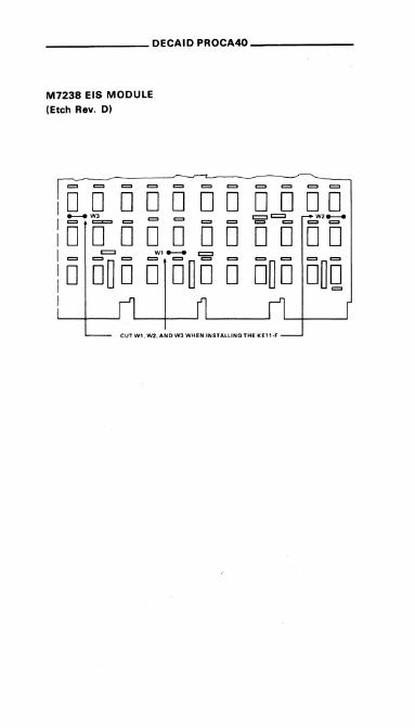
PDP-11/45 VOLTAGE REGULATOR CONFIGURATION DATA CABINET SERIAL NUMBERS 2000 AND HIGHER
Regulator Type Name Quantity Location Comments
Basic System
H744 +5V 3 B +5 V to CPU modules slots 6-9.
C +5 V to CPU and KT11-C modules.
slots 1 0-1 5.
D +5 V to internal options, slots 26-28, system units 1, 2, and 3, and console.
H745 -15 V 1 F -15 V to CPU and internal option modu-
les. This supply is switched, even in the lower H742, because it is fed by + 1 5 Vdc frol)1 the upper H742.
FP11-B Floating Point Processor
H744 +5V 1 A +5 V to FP11 modu-
les, slots 2-5.

DECAID PWRB-2
PDP-ll/46 VOLTAGE REGULATOR CONFIGURATION DATA CABINET SERIAL NUMBERS 2000 AND HIGHER (CONT)
Regulator Type Name Quantity Location Comments
MSll-C Bipolar Memory
H744 +5V 2 H.J +5 V to control and
matrix modules if no MOS memory is
installed. or only 4K is used. H: slots 16-18;
J: slots 19-20.
2 K. L If MOS memory is also installed. or if more than 4K of bipo-
lar is used. K: slots 21 -23. L: slots 24-25.
MSll-B MOS Memory
H744 +5V 1 J +5 V to control and
matrix modules. slots 16-25.
H746 MOS ~ H.L +19.7 V. +23.2 V. and -5 V to MOS mat-rix modules; H slots 17-20; L slots 22-25.
MMll Core Memories and Controls
H745 -15V 1 E -15 V to system units 1-3.
H754 +20.-5V1 E 20 and -5 Vdc to
MF11-U/UP. No -15
Vdc available for other
system units.

DECAID PWRB-2
PDP-11/46 VOLTAGE REGULATOR CONFIGURATION DATA
CABINET SERIAL NUMBERS LESS THAN 2000
Reguleto Type Name Quantity Location Comments
Basic System
H744 +5V 3 B +5 V to CPU modu· les, slots 6-9.
C +5 V to CPU and
KT11-C modules,
slots 10-1 5.
D +5 V to internal options, slots 26-28,
system units 1, 2, and
3, and console.
H475 -15V 1 E -15 V to CPU and
internal option modu· les and system units 1
and 2.
FP11-B Floating Point Processor
H744 +5V 1 A +5 V to FP11 modu· les, slots 2-5.
MSll-C Bipolar Memory
H744 +5V 2 H,J +5 V to control and
matrix modules if no
MOS memory is
installed, or only 4K is
used. H: slots 16-1 B:
J: slots 19-20.

DECAID PWRB-2
PDP-11/46 VOLTAGE REGLATOR CONFIGURATION DATA CABINET SERIAL NUMBERS LESS THAN 2000 (CONTI
Regulato Type Neme Quantity Locetion Comments
2 K. L If MOS memory is also installed. or if more than 4K of bipo-lar is used. K: slots 21-23. L: slots 24-25.
MS11-B MOS Memory
H744 +5V 1 J +5 V to control and matrix modules. slots 16-25.
H746 MOS 2 H.L +19.7 V. +23.2 V. and -5 V to MOS mat-rix modules; H slots 17-20; Lslots22-25.
MM11 Core Memories and Controls
H745 -15V 1 F -15 V to system unit 3. ;H745 provided in basic system supplies system units 1 and 2. This supply is switch-ed even in the lower H742. because it is fed by + 15 Vdc from the upper H742.

OECAIO PWRB-2
H744. +5 VOC REGULATOR
POWER INDICATOR
LIGHT
INPUT/OUTPUT
J'

OECAIO PWRB-3
CROWBAR PROBLEMS
As you are powering the machine on and off (or for various other mysterious reasons). it can happen that one or more of the regulators may crowbar. That is, the regulator short circuits its output to protect the load. The output of a crowbarred regulator would be seen as approximately 0 V.
To check for this, first power the machine down. (This is very important: otherwise the crowbar circuit will not reset.) Then rotate the adjustment potentiometer of the offending regulator(s) counterclockwise a half revolution. Turn the power back on and observing the voltage level with a scope on the backplane pin, readjust the potentiometer so that the regulator is providing the correct output.
If you can't adjust the regulator's output to the correct level, then something else is causing the fault. Continue on the PWRB flows.
If you find that the regulator crowbars again after this procedure, then you have something connected to the regulator's output that is causing it to go too high. This is often due to a poor connection in one of the connectors in the power harness. Work the connectors firmly into their sockets and manipulate the wires going into the connectors.
Also look for possibilities such as a loose piece of wire shorting out a couple of backplane pins or else a backplane pin that is bent and is touching a neighboring pin.

DECAID PWRB-4
DISTRIBUTION PANEL CONNECTORS
The following diagrams show the locations of the pins carrying the
power and signals into and out of the various distribution panels
used on all models of the PDP-11/40 and PDP-11/45 processors.
Check for these voltages by wedging the scope probe down into the connectors pin socket so that the probe makes connection with the
pin inside the socket.
Note that the pin layout for the distribution panel supplying power
to the system units on PDP-11 145s with serial numbers 2000 and
higher is the same as the one for distribution panels used on PDP-11/40s with serial numbers 6000 and higher.
PDP-11/40 DISTRIBUTION PANEL CONNECTORS FOR SERIAL NUMBERS 6000 AND HIGHER
<:: CONSOLE
i)~ LJ~
r-....., , 2 3
4 • • 7 • • ,. " '2
'3 '4 ,.
'-..../
1. GND tBlKI 2. LINE eLK IBANI 3. DC LO (VIOl 4. AC LO lYELI 6. SPARE e. SPARE
1. +6vIREDI 2. +15V(GRVI 3. +20V lOAN) 4. +&V(REDI S. GND tBlKJ 6. SPARE 7. GNDIBLKJ 8. ONDIBLKJ 9. GND (BlK) 10. SPARE
". OND CBlK) 12. SPARE 13. -16VIBLUI
'4. -&VIBRNJ 15. SPARE
(Continued)

DECAID PWRB-4
In the mainframe box's distribution panel there are four groups con
taining five pairs as shown above. Within a group, all pairs are bussed together pin-for-pin by the distribution panel. Each connector
mayor may not have all the above-listed wires connected to it.
PDP-11/40 DISTRIBUTION PANEL CONNECTORS FOR
SERIAL NUMBERS LESS THAN 6000
<:: CONSOLE
B ~ , 2 3
, 2 3
4 5 6
~
12 11 ,'0
• • 7
4 5 6 7 • • 6 5 4
7 • • '0 11 12 3 2 ,
u '---J 1 DC LO (VIO) 1 -15V(BLU) 1 SPARE
2. AC LO (VEL) -15V(BLU) 2. LINE eLK (BRN!
3. -15V(8LUj GND (BlK) 3 liNE eLK (BRN)
4. GNe (BlK) 4 GND (eLK) SPARE
5 SPARE 5. GND (eLK) GND (BlK)
6. SPARE 6. GND (BlK) 6 GND (BLK)
7 LINE eLK(BRN) 7. +5V (RED) 7 DC LO (VIO) •. +15V(GRY) •. GND (BLK) 8. SPARE •. +5V (RED) • GND (BLK) .. SPARE 10 +5V (REO) 10 DC LO (VIO)
TO BACKPLANE 11. +15V(VIOJ 11 AC LO (YEL)
12. +15V(VIO) 12 AC LO (YEL)
FROM REGULATORS
In the mainframe box's distribution panel. there are three groups
each containing five connectors, that is, the two 12-pin connectors
shown above and three of the 9-pin connectors shown above. With
in a group, all three 9-pin connectors are bussed together pin-forpin by the distribution panel. Each connector mayor may not have
all the above-listed wires connected to it.

TO SYSTEM U"IIT5 'V HAR"IE:5S 7008784 C
(5/"1 < 2.000}
~ ~
...... .,. U1
III :I> n ;0: 'V ,... :I> Z C m m
n n !: 0 z c Z 'V m :E n :Jl -I III 0 ,i. :Jl (I)
:I> Z c :!! z (I)

DECAID PWRB-4
INSTALLATION OF SYSTEM UNITS, LATER SYSTEMS, PDP-11/46 CABINET SERIAL NUMBERS 2000 AND HIGHER
THE PIN lA'tOur FOR THIS DISTRIBUTION PANEL IS THE SAME AS THE ONE USED ON" 140', WITH SERIAL NUMBERS 6000 AND HIGt4ER

DECAID PWRB-4
INSTALLATION OF SYSTEM UNITS, EARLY SYSTEMS, PDP-11/45 CABINET SERIAL NUMBERS LESS THAN 2000
G772A PC BOARD
SEE "OTE 1
7008784 POWER HARNESS
NOTE Inoom. ",'em"MS, • ..e~ •• MMll-S,G772ApluU iMO .'01 C04;o~oIne' opl1o",. 1103" i ...... d
~fc~~ ,:i:~~~!t::,':.'t1e ..
(p;n.,dtoISj"t", u",1 po"" sl.')
LINE CLOCK
-

DECAID PWRB-5
POWER HARNESSES AND CABLES
Before you replace any of the cables or harnesses. ensure that the connectors are making a solid electrical connection. Firmly work the connectors into their sockets and manipulate the wires at the connectors while looking for any changes in the problem symptoms. If this procedure causes a change. then it may only be necessary to reset the connectors in their sockets or the pins in their connectors.
If you find that it is necessary to replace any cables. refer to the following pages of this DECAID to make sure that you obtain the correct replacement.
Present and future power handling capabilities of the 11/40-11/45 CP expander boxes and H960D. E cabinets have been increased with the creation of two new main power harnesses.
Along with this comes a whole new set of option cables necessary to connect our existing options to this new power configuration.
New and old machines may be easily identified by visually
inspecting their serial number affixed to the expander box or by noting the new main power harness that is installed within the expander box.
Serial numbers> 6000 indicate a new PDP-11/40 power configuration « = old type).
Serial numbers > 6000 indicate a new H960D. E power configuration « = old type).
Serial numbers> 2000 indicate a new PDP-11/45 power configuration « = old type).
The following tables list the options and CPU power harnesses affected by this change. Also included are the part numbers for other power cables not affected along with remote sense and intermodule cables used in the PDP-11 world.

DECAID PWRB-6
POWER DISTRIBUTION HARNESS (Power Supply to Distribution Points)
Description
PDP-11/15, PDP-11/20
8A11-ES
PDP-11/05 NC, PDP-11/35 10-1/2-inch box
PDP-11/45, PDP-11/50 (Old)
PDP-11/40 and H960D/E (Old)
PDP-11/45 and PDP-11/50 (New)
PDP-11/40 and H960D/E (New)
Cable
70-6518
70-5894
70-9208
70-8784
70-8754
70-9540
70-9566
• There will be some units between serial number. 6000 and 6542 that will still have the old configuration.

DECAID PWRB-6
DC DISTRIBUTION TO CPU BACKPLANE
Description Cable
PDP-ll/05S 70-9918
PDP-ll/05 NC 70-9360 PDP-ll/10 1O-1/2-inch box
PDP-11/35 70-9209
PDP-11/40 70-9046 (Old)
PDP-11/45 N/A
PDP-11/40 70-9564 (New)
PDP-11/35S 70-10113
NOTE If a new PDP-11/35-PDP-11/40 backplane is ordered (part no_ 70-10230), you must order 70-9994 cable for new-style PDP-11/40s. For old-style PDP-11!40s, use original cable cut to length.

_______ DECAID PWRB·5
REMOTE SENSE CABLES
Description Cable
861 Remote Sense Cable (11/40 to 861) 70·9053
861/860 Remote Sense Cable (861/860 70·8288 to 861/860)
861/860 Remote Sense Cable (861/860 70·8964
to 1 st H720E/F)
H720E/F to H720E/F Remote Sense
Cable 70·8288
H720E/F (J2) Remote Sense Terminator 70·7006·1
Plug
H 720E/F (J 1) Local Sense Jumper Plug 70·7006·2
INTER·MODULE CABLES
CPU Type Description Cabla
PDp·ll/05 Console Cable BC08R·3 (5·1/4 inch)
PDp·ll/05 Console Cable BC08R·4
(10·1/2 inch)
PDp·ll/35 Console to K 1 and K5 (2) BC08R·3 PDp·ll/35·11/4Q KEll·E BC08R·l
(M7238 to M7232) (3)
PDp·ll/4Q Console to K 1 and K5 (2) BC08R·6
PDP·l1/45 Console Cable (2) 70·8864

_______ DECAID PWRB-5
OPTIONS
11/35S, 11 /05S CPU Type 11/05,11/10 11/35 BAll-KE/F Optioo 10-112-10. 10-1/2-10. 10-1/2-10.
Box Box Box
AA11-0A 70-9205 70-9205 70-9562 AA11-0B 70-9205 70-9205 70-9562 OAll-F 70-9099 70-9099 70-10117 OBll-A 70-9205 70-9205 70-9562 OC11-A 70-9205 70-9205 70-9562 0011-A 70-9205 70-9205 70-9562 0011-B 70-9099 70-9099 70-10117 OH11-AA N/A N/A 70-10118 OHll-AB N/A N/A 70-10118 OHll-AC N/A N/A 70-10118 OJll-AA 70-9099 70-9099 70-10117 OJ11-AB 70-9099 70-9099 70-10117 OJ11-AC 70-9099 70-9099 70-10117 ON11-AA 70-9205 70-9205 70-9562 OPll-0A 70-9205 70-9205 70-9562 OR11-B 70-9205 70-9205 70-9562 MF11-L 70-9206 70-9206 70-10114 MF11-LP N/A 70-9206 70-10114 MF11-U/UP N/A N/A 70-10115 MMll-S 70-9205 70-9205 70-9562 RHll 70-9099 70-9099 70-9570 RHll-AB 70-9099 70-9099 70-10117 RK11-0 70-8992 70-8992 70-10116 VT11 70-9099 70-9099 70-10117 COll-AiB/E 70-9099 70-9099 70-10117 0011 70-9099 70-9099 70-10117

DECAID PWRB·6 ______ _
OPTIONS
11/40 CPU Type 11/46 H960D. E Option (Old) (Old)" "
AAll·DA 70·8855·1J 70·8909·XX AAll·DB 70·8855·1J 70·8909·XX DAll·F 70·9162 70·9099 DBll·A 70·8855·1J 70-8909·XX DCll-A 70-8855-1J 70-8909·XX DD11-A 70-8855 70·9177
70·8909-XX DD11·B 70-9162 70·9099 DHll·AA N/A 70·9466 DHll-AB N/A 70·9466 DHll-AC N/A 70·9466 DJ11-AA 70-9162 70·9099 DJ11-AB 70-9162 70-9099 DJ11-AC 70-9162 70·9099 DNll-AA 70·8855·1J 70·8909-XX DPll-DA 70-8855-1J 70·8909-XX DRll-B 70-8855-1J 70·8909-XX MF11-L* 70·9242 70·9103 MFll-Lt N/A 70-9174 MFll-LP* 70-9242 70-9103 MF11-LPt N/A 70-9174 MFll-UlUP:j: N/A N/A MMll-S 70-8855-2B 70·8909·XX RHll 70-9162 70·9571 RH11-AB 70·9162 70·9099 RK11-D 70·8855·1J 70·8992 VTl1 70-9162 70-9099 CDll-A/B/E 70·9162 70·9099 DOll 70·9162 70·9099
PDP·11/40 only (1st MFll·LlLP). t PDp·11/40 only (2nd MF11·LlLP).
11/40.11/46 H960D/E (New)
70·9562 70·9562 70·9563 70-9562 70·9562 70-9562
70-9563 70-9561 70-9561 70-9561 70·9563 70-9563 70-9563 70-9562 70-9562 70-9562 70-9565 70-9560 70·9565 70·9560 70·9535 70-9562 70-9570 70·9563 70-9559 70·9563 70·9563 70·9563
:I: MF11·U/UP cannot be mounted in old style PDP·11/45 CPU box ..
70·8909·XX cable has two variations - 11 inches and 17 inches. Usa 70·9177 if due to new module guide layout; 70·89og·XX cables are too
short.

DECAID PWRB·6
PIN LOCATIONS FOR REGULATOR'S CONNECTORS
~ ~~ 871554321
~ 8 • • • • • • • •
H744 H746
1. Spare 1. -1 5 V output (blue)
2. +5 V output (red) 2. GND (black)
3. GND (black) 3. GND (black)
4. GND (black) 4. + 15 V input (violet or gray)
5. +5 V output (red) 5. + 1 5 V input (violet or gray)
6. 20-30 Vac input (red) 6. 20-30 Vac input (red)
7. 20-30 Vac input (white) 7. Spare
8. Spare 8. 20-30 Vac input (white)
H754 H746
1. Spare 1. Spare 2. GNO (black) 2. GND 3. -5 V output (brown) 3. -5 V output 4. Spare 4. +19.7 V output 5. +20 V output (orange) 5. +23.2 V output 6. Spare 6. Spare 7. 20-30 Vac input (red) 7. 20-30 Vac input 8. 20-30 Vac input (white) 8. 20-30 Vac input

DECAID PWRB-7
PROCEDURE FOR REMOVAL OF REGULATORS
1. Turn the power off at the circuit breaker on the 860/861 Power Controller.
2. Disconnect the connector at the top of the regulator.
3. Remove the two Phillips screws on top of the regulator which hold the regulator in the H742 box.
4. Loosen the finger-tight (usually) screw on the bottom of the regulator.
5. Slide the regulator out horizontally away from the H742 box.
The following diagram shows the location of the fuse. Usually you
can check it without taking off the clear plastic cover. It is an AGC 15-amp fuse.
+5 V REGULATOR, SIDE VIEW

DECAID PWRB-B
H742 CONNECTORS FOR PDP-ll/40
As seen from the back, the connectors on the H742 Power Supply are located as shown in the diagram below.
P8 Pl0
o P9 CJ o
The following pages list the functions and locations of each of the
pins on the abo,ve three connectors.
PDP-ll/40 Pin Locations for H742's Connectors
P8
3 6 9
2 5 8
1 4 7
Function Pin(s) (Vac) Color Dest,
1-2 (new) 20-30 Red, white Slot B
1-2 (old) 20-30 Red, white SlotA
3-4 20-30
5-6 20-30
7-8 20-30 Red, white Slot D

_______ DECAID PWRB-8
PDP-11/40 Pin locations for H742's Connectors ICont)
P9
3 6 9 12
2 5 811
1 4 7 10
Pin Is) Function Color Dast.
+8V
2 +15V Gray or Cist. Panel violet
3 +15V Gray or Slot C violet
4 GNC Black Slot 0
5 GNO Black Slot E
6 GNC Black Cist. Panel
7 GNC Black Cist. Shield
8 AClO Yellow or Cist. Panel red
9 CClO
10 AClO
11 LINE ClK Brown or Cist. Panel black
12 CClO Violet or Cist. Panel clear

DECAID PWRB-8
PDP-11140 Pin Locations for H742's Connectors (Conti
Pl0
3 6 912 15
2 5 811 14
1 4 710 13
Function Pin(s) (Vac) Color Dest.
1-2 (new) 20-30 Red. white SlotA
1-2 (old) 20-30 Red. white Slot B
8-10 20-30 Red. white Siote
9-12 20-30 Red. white Slot E
3-7 115 Red. white H742 fan
5-6 115 Red. white Proc. fans

DECAID PWRB-B
UPPER H742 CONNECTORS FOR PDP-11145
As seen from the back. the connectors on an upper H742 Power Supply are located as shown in the diagram below.
P16 P15
D P14 CJ o
The following pages list the fUnctions and locations of each of the
pins on the above three connectors.
PDP-11/45 Pin Locations for Upper H742's Connectors
P16
~ 6 9
2 5 8
1 4 7
Function Pin(s) (Vac) Color Dest.
1-2 20-30
3-4 20-30 Red. white Slot B
5-6 20-30
7-8 20-30 Red. white Slot C

DECAID PWRB-8
PDP-11/45 Pin Locations fOf Uppef H742's Connectors (Cont)
P14
3 6 9 12
2 5 B 11
1 4 7 10
Pin(s) Function Col Of Dest.
+BV White Dist. Panel
2 (new) +15V Gray Slot F
2 (old) +15V Gray Slot E
3 +15V Gray Dist. Panel
4 GND Black Slot E
5 GND Black Dist. Panel
6 GND Black Slot F
7 GND Black Dist. Panel
B AClO Yellow Dist. Panel
B AClO Yellow Lower H742
9 (new) DC lO
9 (old)
10 AClO Yellow Dist. Panel
10 AClO Yellow lower H742
11 LINE ClK Brown Expn.Dist.
12 DC lO Violet Dist. Panel

_______ DeCAID PWRB-B
PDP-11!46 Pin Locations for Upper H742's Connectors (Cont)
P16
3 6 9 12 15,
2 5 811 14
1 4 7 10 13
Function Pin(s) (Vac) Color Dest.
1-2 20-30 Red. white SlotA
8-10 20-30 Red. white Slot 0
9-12 20-30 Red. white SlotE
3-7 115 Red. white H742 fan
5-6 115 Red. white Time meter

OECAIO PWRB-8
LOWER H742 CONNECTORS FOR POP-11146
As seen from the back. the connectors on a lower H742 Power Supply are located as shown in the diagram below.
P24 P23
D ~ P22
o
The following pages list the functions and locations of each of the pins on the above three connectors.
POP-11/46 Pin Locations for Lower H742's Connectors
P24
3 6 9
2 5 8
1 4 7
Function Pinls) IVac) Color Oest.
1-2 20-30 Red. white SlotJ
3-4 20-30
5-6 20-30 Red. white SlotH H746
7-8 20-30 Red. white SlotH H744

DECAID PWRB-8
PDP-11/46 Pin Locations for Lower H742's Connectors (Cont)
P22
3 6 9 12
2 5 811
1 4 7 10
Pin(s) Function Color Dest.
3 GND Black Dist. Panel
4 -15V Blue Dist. Panel
7 GND Black Dist. Panel
8 AC LO Yellow Upper H742
9 DC LO Violet Dist. Panel
10 AC LO Yellow Upper H742
12 DC LO Violet Dist. Panel

DECAID PWRB-8
PDP-11/45 Pin Locations for Lowar H742's Connectors (Cont)
P23
3 6 9 12 15
2 5 811 14
1 4 7 10 13
Function Pin(s) (Vac) Color Dest.
1-2 20-30 Red. white Slot L
8-10 20-30 Red. white Slot K
9-12 20-30 Red. white Slot F
5-6 115 Red. white Proc. fans
3-7 115 Red. white H742 fan

DECAID PWRB-9
PROCEDURE TO CHECK THE FUSE AND TO REMOVE THE POWER CONTROL BOARD WITHIN THE H742 POWER
SUPPLY
CAUTION You are working with 115 Vac. Be very
Sure to disconnect the H742 from the power source and allow about 1 0 seconds for the capacitors to discharge before starting this procedure.
Lift off the H742's top and side cover (one piece) after removing the two screws located at the front and rear of the power supply box.
Don't pull it away too far as the fan on the cover is conncted to a terminal board in the box.
Check the fuses (5 amp and 114 amp) on the power control board.
The following diagram shows their locations.
If it is necessary to replace the power control board:
Loosen but do not remove· the two screws indicated in the diagram.
Remove the screws indicated.
Disconnect the connector from the board.
Remove the other connector from the box.
Slide out the power control board .
• Do not remove these screws because it is very likely that in trying to put
them back in, you will drop them down into the H742 box.

NOTE LOOSEN DO NOT REMOVE))!
ITWILLBEEASIERT ~H~OU PULL THE IN61~!~~:THIS SCREW H742 BOX, LAMP FORWARD OUT OF
DISCONNECT CONNECTOR
REMOVE CONNECTOR FROM H742 BOX
1/4AMP FUSE HERE or HERE JL __J 5 AMP FUSE
". OOMO~o~ ~ 0 fll
o 0 00
____ ...L_--1_L _______ J Iffi ...... REMOVE
J: .... "" N en "lI 0 :E m :Jl
0 0 Z -! :Jl
C 0
m 0 ....
III ~ 0 C ~ "lI :Jl :E c :Jl
III cD

DECAIDPWRD
PDP-11/05/10 POWER CONNECTORS
See the next page for a diagram shown in the pin locations.
PDP-11/05/10 5-1/4-INCH BOX
Allowabla Voltage Tolerance Ripple
+15V ±5% 750mV +5V ±5% 200mV -15 V ±5% 450mV
PDP-11/05-N, 11/10-N 10-1/2-INCH BOX
Allowable Voltage Tolerance Ripple Regulator
+15V ±5% 500mV 5409728 +5V ±5% 200mV 5409728 -15 V ±5% 450mV 5409728 +5V ±5% 200mV H744
The two + 5 V outputs must not be shorted together. The 5409728 regulator provides +5 V to connectors Jl and J2 on the power
distribution board. The H744 provides +5 V to connectors J3, J4.
and J5. The CPU backplane is normally connected to J1.
PDP-11/05-S, 11/105
Allowable Wire Pin Voltage Tolerance Ripple Color Number
+5V ±5% 200mV Red 1.4 +15V ±10% Gray 2 +20V ±5% 100 mV Orange 3 -15 V ±5% 450mV Blue 13 -5V ±5% 250mV Brown 14

ADJUSTMENT POTENTIOMETERS
CP·2004
C m n )10
c ." ::E :II C

DECAID REMOTE ______ _
REMOTE POWER CONTROL FACILITY
All PDP-ll computers have provisions to allow the console switch
to control the operation of the cabinet mounted 860/861 Power Controllers and H720 Power Supplies.
These devices should be connected together with the remote power
control bus which is a 3-wire system with the wires having the
functions shown below:
Q),. REMOTE TURN ON ,REOJ
o 2. EMERGENCY SHUTDOWN (BLK)
o 3. SIGNAL RETURN (GRNI
POWER CONTROL OPERATION
Connections Switch Position
Between Local Off Remote
Control Switched Switched Switched
lines Power Is Power Is Power Is
None On Off Off
1-3 On Off On
2-3 Off Off Off
1-3.2-3 Off Off Off
See DECAl D PWR 8-5 for a list of the remote sense cables used to
connect various power components.

DECAID START
SUGGESTIONS ON WHAT TO DO BEFORE ACTUAL HARDWARE TROUBLESHOOTING
Before you go to the customer's site:
1. Find out as much about the system configuration as you can.
Which CPU How much memory. what type
What mass storage devices. how many of each
What software
What other peripherals. how many of each
What communications equipment. etc.
2. Read the last few Field Service Reports for this system to
see if the problem is a recurring one or if it may be related to
some work that was done recently.
When you get to the customer's site:
1. Question (gently) the user to find out as much about the
failure as possible.
What was the system doing when it failed?
Was there any smoke. sparks. noises. etc.?
What software was running?
How many users were on the system?
Have there been any recent changes to the hardware or
software?
2. Check the obvious and simple possibilities first.
Power plugs not inserted properly
Cables hanging loose
Physical damage


![Pioneer Pdp 434cmx Pdp 43mxe1 s [ET]](https://img.dokumen.tips/doc/110x75/55cf8eae550346703b948a48/pioneer-pdp-434cmx-pdp-43mxe1-s-et.jpg)
![Panasonic 2012 PDP Troubleshooting Guide ST50 ST Series [TM]](https://img.dokumen.tips/doc/110x75/55cf970d550346d0338f80a6/panasonic-2012-pdp-troubleshooting-guide-st50-st-series-tm.jpg)