Embed Size (px)
Citation preview

IRG4BC30FD-SPD - 96929
www.irf.com 1
=
E
G
n-channel
C
Fast CoPack IGBTINSULATED GATE BIPOLAR TRANSISTOR WITHHYPERFAST DIODE
Features ! "#$ %&$'( ) * +$ ,#&$'( -./-011 ) +11 1 * #
$ %&$'(2 +)1*1 #&$'(2 1#-./-0 &$'(2# 3 ) + 1 4**#0 * 55 1 )1 +$ ,&/&$'(2#
D2Pak
Absolute Maximum RatingsParameter Max. Units
VCES Collector-to-Emitter Voltage 600 V
IC @ TC = 25°C Continuous Collector Current 31
IC @ TC = 100°C Continuous Collector Current 17 A
ICM Pulse Collector Current (Ref.Fig.C.T.5) 120
ILM Clamped Inductive Load current 120
IF @ TC = 100°C Diode Continuous Forward Current 12
IFM Diode Maximum Forward Current 120
VGE Gate-to-Emitter Voltage ±20 V
PD @ TC = 25°C Maximum Power Dissipation 100 W
PD @ TC = 100°C Maximum Power Dissipation 42
TJ Operating Junction and -55 to +150 °C
TSTG Storage Temperature Range
Thermal / Mechanical CharacteristicsParameter Min. Typ. Max. Units
RθJC Junction-to-Case- IGBT ––– ––– 1.2 °C/W
RθCS Case-to-Sink, flat, greased surface ––– 0.50 –––
RθJA Junction-to-Ambient (PCB Mounted,steady state) ––– ––– 40
Wt Weight ––– 2.0 (0.07) ––– g (oz.)

IRG4BC30FD-S
2 www.irf.com
Electrical Characteristics @ TJ = 25°C (unless otherwise specified)Parameter Min. Typ. Max. Units
V(BR)CES Collector-to-Emitter Breakdown Voltage 600 — — V VGE = 0V, IC = 250µA
∆V(BR)CES/∆TJ Temperature Coeff. of Breakdown Voltage — 0.69 — V/°C VGE = 0V, IC = 1mA
— 1.59 1.8 IC = 17A VGE = 15V
VCE(on) Collector-to-Emitter Voltage — 1.99 — V IC = 31A See Fig. 2, 5
— 1.7 — IC = 17A, TJ = 150°C
VGE(th) Gate Threshold Voltage 3.0 — 6.0 V VCE = VGE, IC = 250µA
∆VGE(th)/∆TJ Threshold Voltage temp. coefficient — -11 — mV/°C VCE = VGE, IC = 250µA
gfe Forward Transconductance 6.1 10 — S VCE = 100V, IC = 17A
ICES Zero Gate Voltage Collector Current — — 250 µA VGE = 0V, VCE = 600V
— — 2500 VGE = 0V, VCE = 600V, TJ = 150°C
VFM Diode Forward Voltage Drop — 1.4 1.7 V IF = 12A See Fig. 13
— 1.3 1.6 IF = 12A, TJ = 150°C
IGES Gate-to-Emitter Leakage Current — — ±100 nA VGE = ±20V
Switching Characteristics @ TJ = 25°C (unless otherwise specified)Parameter Min. Typ. Max. Units
Qg Total Gate Charge (turn-on) — 51 77 IC = 17A
Qge Gate-to-Emitter Charge (turn-on) — 7.9 12 nC VCC = 400V See Fig. 8
Qgc Gate-to-Collector Charge (turn-on) — 19 28 VGE = 15V
td(on) Turn-On delay time — 42 — TJ = 25°C
tr Rise time — 26 — ns IC = 17A, VCC = 480V
td(off) Turn-Off delay time — 230 350 VGE = 15V, RG = 23Ωtf Fall time — 160 230 Energy losses inlcude "tail" and
Eon Turn-On Switching Loss — 0.63 — diode reverse recovery.
Eoff Turn-Off Switching Loss — 1.39 — mJ See Fig. 9, 10, 11, 18
Ets Total Switching Loss — 2.02 3.9
td(on) Turn-On delay time — 42 — TJ = 150°C See Fig. 9,10,11,18
tr Rise time — 27 — ns IC = 17A, VCC = 480V
td(off) Turn-Off delay time — 310 — VGE = 15V, RG = 23Ωtf Fall time — 310 — Energy losses inlcude "tail" and
Ets Total Switching Loss — 3.2 — mJ diode reverse recovery.
LE Internal Emitter Inductance — 7.5 — nH Measured 5mm from package
Cies Input Capacitance — 1100 — VGE = 0V
Coes Output Capacitance — 74 — pF VCC = 30V See Fig. 7
Cres Reverse Transfer Capacitance — 14 — f = 1.0MHz
trr Diode Reverse Recovery Time — 42 60 ns TJ = 25°C See Fig.
— 80 120 TJ = 125°C 14
Irr Diode Peak Reverse Recovery Current — 3.5 6.0 A TJ = 25°C See Fig.
— 5.6 10 TJ = 125°C 15
Qrr Diode Reverse Recovery Charge — 80 180 nC TJ = 25°C See Fig.
220 600 TJ = 125°C 16
di(rec)M/dt Diode Peak Rate of Fall of Recovery — 180 — A/µs TJ = 25°C See Fig.
During tb — 120 — TJ = 125°C 17
VR = 200V
di/dt 200A/µs
Conditions
Conditions
IF = 12A

IRG4BC30FD-S
www.irf.com 3

IRG4BC30FD-S
4 www.irf.com

IRG4BC30FD-S
www.irf.com 5

IRG4BC30FD-S
6 www.irf.com

IRG4BC30FD-S
www.irf.com 7

IRG4BC30FD-S
8 www.irf.com
Same typedevice asD.U.T.
D.U.T.
430µF80%of Vce
t1
Ic
Vce
t1 t2
90% Ic10% Vce
td(off) tf
Ic
5% Ic
t1+5µS
Vce ic dt
90% Vge
+Vge
∫Eoff =
!"
∫ Vce ie dtt2
t1
5% Vce
IcIpkVcc
10% Ic
Vce
t1 t2
DUT VOLTAGEAND CURRENT
GATE VOLTAGE D.U.T.
+Vg10% +Vg
90% Ic
trtd(on)
DIODE REVERSERECOVERY ENERGY
tx
Eon =
∫Erec =t4
t3Vd id dt
t4t3
DIODE RECOVERYWAVEFORMS
Ic
Vpk
10% Vcc
Irr
10% Irr
Vcc
trr ∫Qrr =
trr
tx id dt
!"
!"
6&6 &
&
6 &

IRG4BC30FD-S
www.irf.com 9
Vg GATE SIGNALDEVICE UNDER TEST
CURRENT D.U.T.
VOLTAGE IN D.U.T.
CURRENT IN D1
t0 t1 t2
D.U.T.
V *c
50V
L
1000V
6000µF 100V
Fig. 19 - Clamped Inductive Load Test Circuit Fig. 20 - Pulsed Collector CurrentTest Circuit
Fig.18e - Macro Waveforms for Figure 18a's Test Circuit

IRG4BC30FD-S
10 www.irf.com
" #$ %% &# '
!
IRG4BC30FD-S
www.irf.com 11
Notes:()*+,-)% $.#%./012)&+,'
!,%('+,3,45(+6Ω &7'
8% $.# ≤ !,4 -.0 ≤ , 9.
8% $.# ,4 % #
When mounted on 1" square PCB (FR-4 or G-10 Material).
Data and specifications subject to change without notice.
IR WORLD HEADQUARTERS: 233 Kansas St., El Segundo, California 90245, USA Tel: (310) 252-7105TAC Fax: (310) 252-7903
Visit us at www.irf.com for sales contact information. 12/04
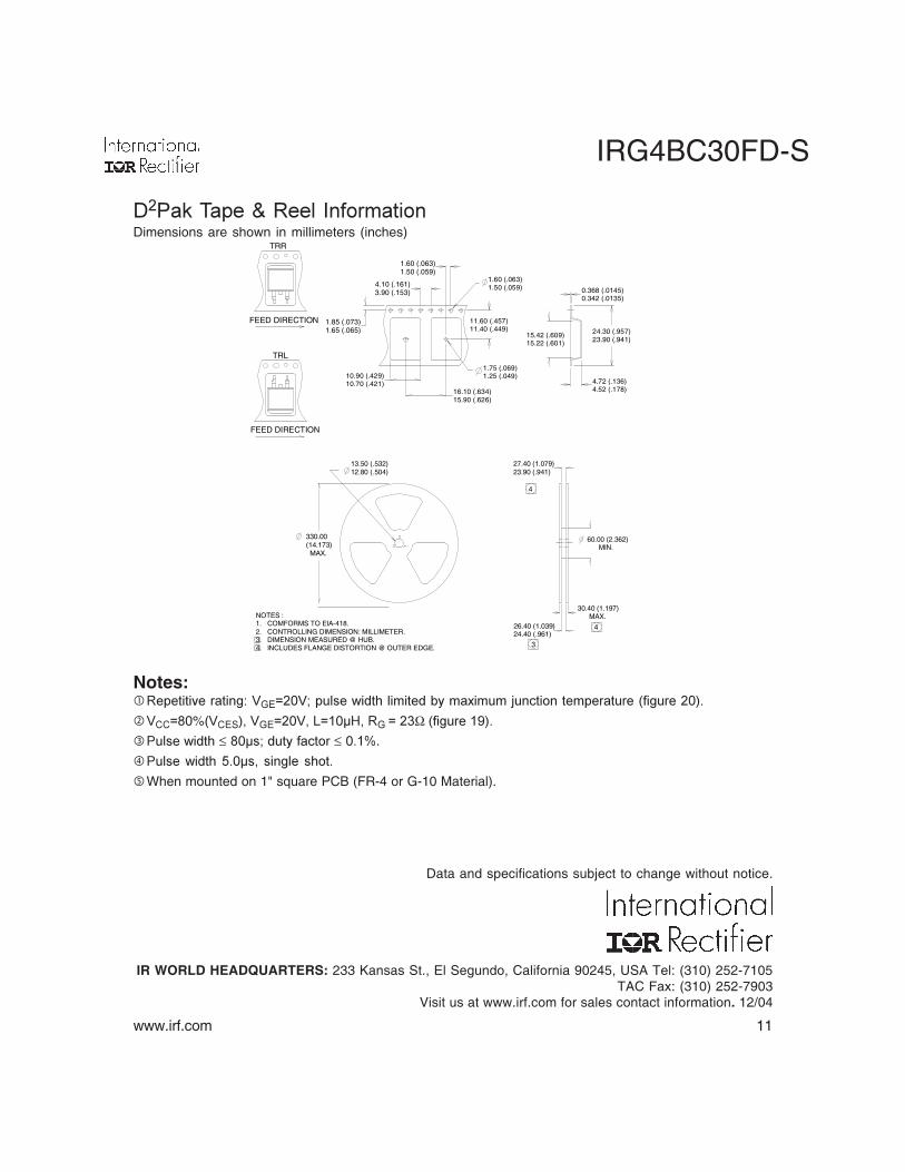
Dimensions are shown in millimeters (inches)
3
4
4
TRR
FEED DIRECTION
1.85 (.073)1.65 (.065)
1.60 (.063)1.50 (.059)
4.10 (.161)3.90 (.153)
TRL
FEED DIRECTION
10.90 (.429)10.70 (.421)
16.10 (.634)15.90 (.626)
1.75 (.069)1.25 (.049)
11.60 (.457)11.40 (.449)
15.42 (.609)15.22 (.601)
4.72 (.136)4.52 (.178)
24.30 (.957)23.90 (.941)
0.368 (.0145)0.342 (.0135)
1.60 (.063)1.50 (.059)
13.50 (.532)12.80 (.504)
330.00(14.173) MAX.
27.40 (1.079)23.90 (.941)
60.00 (2.362) MIN.
30.40 (1.197) MAX.
26.40 (1.039)24.40 (.961)
NOTES :1. COMFORMS TO EIA-418.2. CONTROLLING DIMENSION: MILLIMETER.3. DIMENSION MEASURED @ HUB.4. INCLUDES FLANGE DISTORTION @ OUTER EDGE.

Note: For the most current drawings please refer to the IR website at: http://www.irf.com/package/