Embed Size (px)
Citation preview

IEEE TRANSACTIONS ON POWER ELECTRONICS, VOL. 18, NO. 4, JULY 2003 937
PCB Integrated Inductors for Low PowerDC/DC Converter
Matthias Ludwig, Student Member, IEEE, Maeve Duffy, Member, IEEE, Terence O’Donnell, Member, IEEE,Paul McCloskey, and Seán Cian Ó Mathùna
Abstract—This paper discusses the use of printed circuit board(PCB) integrated inductors for low power dc/dc buck converters.Coreless, magnetic plates and closed core structures are comparedin terms of achievable inductance, power handling and efficiency ina footprint of 10 10mm2. The magnetic layers consist of electro-plated NiFe, so that the process is fully compatible with standardPCB process. Analytic and finite element method (FEM) methodsare applied to predict inductor performance for typical currentwaveforms encountered in a buck converter. Conventional mag-netic design procedures are applied to define optimum winding andcore structures for typical inductor specifications. A 4.7 H PCBintegrated inductor with dc current handling of up to 500 mA ispresented. This inductor is employed in a 1.5 W buck converterusing a commercial control integrated circuit (IC). The footprintof the entire converter measures10 10 mm2 and is built on topof the integrated inductor to demonstrate the concept of integratedpassives in power electronic circuits to achieve ultra flat and com-pact converter solutions.
Index Terms—Electroplating, embedded PCB magnetics, inte-grated magnetics, low power conversion, magnetic design study,ultra flat inductors.
I. INTRODUCTION
T YPICALLY, converters in the 1–2 W range are builtaround dc/dc converter-chips, and these generally require
a small number of additional energy storage componentsincluding an inductor [1]. Ideally, all components wouldbe fabricated on silicon, to provide a completely integratedsolution. However, while much research has been carried outon the development of integrated magnetics on silicon [2], [3],the technology is generally limited by the high resistance ofthin film conducting tracks. Some work has been carried outon the development of high aspect ratio coils for providingincreased conductor cross section to overcome this problem,but the technology is still being developed [4].
The integration of inductor devices into printed circuit board(PCB) is proposed in this work as an alternative cost effec-tive solution, where in addition to providing interconnection be-tween the converter chip and additional components the PCBalso includes fabrication of the inductor structure. Using a tech-nology described previously by the authors [5], magnetic plates
Manuscript received March 11, 2002; revised February 13, 2003. Recom-mended by Associate Editor K. Ngo.
M. Ludwig, T. O’Donnell, P. McCloskey, and S. C. Ó Mathùna are with theEnergy Processing for ICT, National Microelectronics Research Centre, Cork,Ireland.
M. Duffy is with the Department of Electronic Engineering, National Univer-sity of Ireland, Galway, IRELAND.
Digital Object Identifier 10.1109/TPEL.2003.813757
Fig. 1. Half view of principle PCB integrated inductor structure.
and through-holes are defined to provide a closed-core structurearound PCB integrated windings as shown in Fig. 1. Electro-plated NiFe is used in this case so that all processes required forfabrication of the inductor are PCB compatible. In addition toits ease of processing, the composition was chosen forits well known magnetic characteristics.
PCB integrated winding structures have already been appliedas transformers in power converters [6], but these require the useof resonant circuit topologies to compensate for the low induc-tance values achieved. When integrated magnetic cores are used,two different structures can be observed. Most of the publisheddesigns are toroidal structures where the winding is wrappedaround the core by the use of etching and conductive vias. Com-mercial foil layers have been used to provide the integrated cores[7]. However due to the large resistance of vias, winding lossesare high, and this usually is exacerbated by a requirement for alarge number of turns in toroidal designs. The other possibility ispot core structures where the core is formed around the winding.A screen printing technique has been used to apply a polymerfilled NiZn ferrite core [8]. The use of electroplated NiFe in thiswork removes the need for specialised processes to integrate themagnetic core regions.
In most cases, the focus of papers in this area is on the de-scription of processes developed to provide winding and coreregions, and results are presented for the impedance of com-ponents operating under signal level conditions. The design ofPCB integrated transformer structures with electroplated NiFecores was investigated previously by the authors [9]. In thiswork, the design and application of integrated inductor struc-tures formed by the same technology is described for use indc/dc power conversion. For that purpose, the performance ofdifferent integrated winding and core structures is investigatedin Section II to illustrate the limits imposed by eddy-currentsand magnetic saturation in integrated magnetic core regions. Inparticular, it is shown that while closed core structures provide
0885-8993/03$17.00 © 2003 IEEE

938 IEEE TRANSACTIONS ON POWER ELECTRONICS, VOL. 18, NO. 4, JULY 2003
the highest inductance and efficiency levels per unit footprint,current levels that can be supported are limited by saturation inthe thin core regions required to control eddy-current effects.The design of such structures for given power requirements isdescribed in Section III. Conventional equations for power in-ductor design are applied to define winding and core structuresneeded to support inductor voltage levels. When compared withconventional design where components are limited to standardcore shapes, the definition of integrated winding and core re-gions is limited only by the resolution of available PCB pro-cesses in this case. This provides a means for optimising de-signs in terms of minimum footprint area in a given PCB build.FEA simulation is then used to determine the gap length neededto support dc current levels. Technology and design issues aredemonstrated in Section IV for a 4.7H/500 mA inductor ap-plied in a 1.5 W buck converter operating at 1 MHz. This in-ductor has been fabricated and successfully employed with acommercially available dc/dc converter IC.
II. PCB INTEGRATED INDUCTOR STRUCTURES
The performance of PCB integrated inductor structures forapplication in dc/dc converter circuits is compared in this sec-tion in terms of inductance, current/power handling and losses.In terms of PCB processing, the simplest inductor structure tointegrate is spiral winding turns with no magnetic material in-cluded. While these are widely used in signal level applications,issues of EMI and efficiency limit their application in powerconversion. Magnetic layers have been applied to confine mag-netic fields established around the windings during operation indc/dc conversion [6], and it may be expected that these layerswould act as effective magnetic cores in this case. However, inthis work it is shown that there is little or no improvement in in-ductor performance provided by including layers in aninductor structure over an equivalent coreless structure. With theinclusion of magnetic through-holes as shown in Fig. 1, a moreeffective core structure is provided, and results of inductance,power throughput and efficiency are presented to illustrate therelative advantages achieved.
It should be noted that when compared with conventional fer-rite cores the structure of the PCB integrated core is not fixedto standard core shapes, and therefore both winding and corestructures may be optimized for given requirements. However,it is shown that design is largely determined by the limits ofthe available PCB technology. Further the geometries of thewinding and core are closely linked to each other, and eachchange in parameter for one will affect the other. For example,for integration in a given circuit board, the number of windingand magnetic core layers is limited to the total number of PCBlayers, so that by introducing magnetic layers, there are lesslayers available for defining windings. A similar trade-off is de-scribed in terms of winding and core areas within a given PCBfootprint area. While limits in current and power handling maybe overcome by increasing copper thickness and/or increasinggaps in magnetic cores, such trade-offs are best seen in terms ofmaximum inductance values that can be fitted within a givenfootprint, as these are more tightly limited by the minimum
TABLE ICAPABILITIES OF PCB TECHNOLOGY AVAILABLE
track pitch (i.e. maximum number of turns) that can be pro-duced using PCB photolithography and etching processes [5].Therefore, a comparison of maximum inductor designs within1 cm of a six-layer PCB is presented to illustrate how a closedcore structure as in Fig. 1 provides improved performance overcoreless and magnetic plate structures. Corresponding levels ofcurrent / power handling and efficiency of the resulting struc-tures are also compared to illustrate the capabilities and limitsof PCB integrated inductors in dc/dc conversion applications.
Capabilities of the technology available to the authors aresummarized in Table I. As shown, copper track height is chosenas 70 m (2 oz copper) to allow a maximum current of1 A fora winding temperature rise of less then 45 K [10]. In this way,all structures have the same current capacity in terms of windingthermal limits at least. The limit in number of magnetic layersis explained by the fact that the layers are deposited in-houseafter the winding layers are produced commercially. In additionto the geometrical constraints, limits include saturation and con-ducting properties of magnetic core regions.
Levels of current / power handling and power losses for thestructures are compared assuming operation in a dc/dc buck con-verter switching at 1 MHz. That is, maximum power levels han-dled by the inductor are given as
(1)
where it is seen that power is limited by the inductance value,,and maximum output current level, that can be supported. Forstructures with magnetic material included, inductance, ,is a function of the output (inductor) current as given. Conse-quently, it is shown that while signal inductance values are en-hanced by the introduction of magnetic regions, magnetic sat-uration acts so as to limit inductor power handling at highercurrent levels. Assuming a duty cycle, D, of 0.5, (1) is used inthis section to determine the maximum voltage handled by theinductor, while the maximum current is limited by either thesaturation of the magnetic material or the thermal limit of thewinding [10]. A triangular current ripple value of 30% is as-sumed in all cases and resulting levels of power throughput inthe inductor are compared.
Corresponding power losses are calculated using theharmonic component representation of the inductor currentwaveform. For 30% ac ripple, it is found that the contribution

LUDWIG et al.: PCB INTEGRATED INDUCTORS 939
TABLE IIPROPERTIESCORELESSSTRUCTURE
of harmonics greater than the 1st is less than 5% of the totalloss and can therefore be neglected, giving total losses as
(2)
Where is he first harmonic of the overall resistance of theinvestigated structure. It is important to note that the value of
includes eddy-current losses in the magnetic core mate-rial. For that purpose, electroplated permalloy is assumed tohave a relative permeability, , and conductivity,
m . Core losses due to hysteresis are neglected inthis work. Finally, since the levels of power handled by the dif-ferent structures is different, loss characteristics of the differentstructures are best compared in terms of the inductor related ef-ficiency of the converter as given by
(3)
A. Coreless Inductor
As discussed above, the simplest inductor structure to inte-grate in PCB is a coreless winding, and results are presented inthis case as a benchmark for integrated core structures. Max-imum inductance in a given footprint is achieved by fitting thelargest number of winding turns possible in each of the six PCBlayers. For the available track pitch of 400m, 12 turns maybe fitted in a 10 mm diameter, and impedance values and powerperformance of resulting structure are summarized in Table II.Components of impedance at dc are calculated using analyticformulas and FEA simulation is applied for ac calculations.
It is worth noting that the maximum power handling capa-bility of the inductor is limited only by temperature rise in thiscase, and the efficiency of the inductor is constant for all currentlevels less than 1 A.
B. Inductor With Planar Windings and Magnetic Plates
It is well known that the addition of magnetic plates to ei-ther side of planar winding structures provides enhancement ofinductance values, and further that enhancement increases withincreasing plate thickness, up to a certain level [11]. However,for a given PCB build, the relative benefits of substituting corelayers for winding layers has not previously been investigated.
Fig. 2. Cross section of the planar winding and magnetic plates (FEA model).
Fig. 3. Inductance and power handling for different core plate thickness.
For that purpose, the performance of a structure in which theouter winding layers in the coreless design described above arereplaced with circular permalloy plates is investigated in thissection. In this way, designs for maximum inductance in a 1 cmdiameter are investigated. The cross section of a typical structureas simulated in FEA is shown in Fig. 2 [12]. As the thickness ofthe plates is in the range of 10m whereas the overall structureof the device is in the mm range, special attention must be paidto the mesh of the FEA model.
It has been shown that in order to control eddy-current lossesunder signal level ac conditions, thickness of conducting mag-netic plates should be smaller than one skin depth,, of themagnetic material [4]. For application in a buck converter, how-ever, a significant proportion of loss is caused by dc currents (2).Therefore, it may be expected that by replacing winding turnswith magnetic core regions to provide inductance enhancement,efficiency of the resulting structure may be improved, and fur-ther, that the level of ac loss in magnetic layers with thicknesslarger than one skin depth may be tolerated. In order to investi-gate these effects, the performance1 of the magnetic plate struc-ture is investigated as a function of plate thickness. Results ofinductance and power handling are plotted in Fig. 3. Inductancevalues for nonconducting and unpatterned plates were calcu-lated using analytic formulas, while values for patterned plateswere produced using an axisymmetric FEA simulation. Results

940 IEEE TRANSACTIONS ON POWER ELECTRONICS, VOL. 18, NO. 4, JULY 2003
Fig. 4. Losses and efficiency for different core plate thickness.
for nonconducting plates were included to illustrate the magni-tude of eddy-current effects. The effect of patterning was simu-lated by assigning open circuit conditions to the magnetic plates.Maximum current levels were deduced from maximum levels ofmagnetic flux density computed in FEA simulation, and powerhandling was calculated using (1). In all cases, the point of max-imum flux density was found toward the average radius of mag-netic plates as shown in Fig. 2; i.e., where the maximum mag-netic field intensity, , is established by winding currents.
With the inclusion of eddy-currents, maximum inductancevalues are observed for a magnetic plate thickness equal to oneskin depth, , of the magnetic material; i.e., 5m for electro-plated , as expected. For larger thickness, the induc-tance reduces slightly for a thickness of twice the skin depth,and then remains at this level for larger values. This is explainedby the fact that the energy in the magnetic plates is confined towithin two skin depths of the surface [14]. Similar trends are ob-served for patterned and unpatterned magnetic plates. The largervalues predicted for patterned plates illustrate how patterning re-duces eddy-currents induced in response to axial magnetic fields[13]. It is interesting to see that the maximum inductance is ap-proximately the same as that achieved for a coreless structurehaving the same PCB build.
Obviously, power levels given by (1) are limited by saturationin the magnetic plates when compared with windings havingno magnetic core regions. The increase in capacity with platethickness is attributed to an increase in dc current handling be-fore magnetic saturation occurs, as predicted in FEA simulation.This is seen for values of thickness greater than 10m whereinductance values are approximately constant, and may be ex-plained by a redistribution of magnetic flux between magneticplates and the surrounding air. It is not easily predicted due tothe high reluctance of the thin plates when compared with thatof the surrounding air. However, the results illustrate how platethickness greater than 5m may be applied to support higherpower levels (at reduced inductance) if the footprint availablefor integration is limited.
Results of losses and efficiency for the structure calculatedunder the conditions of maximum power handling predicted inFig. 3 are presented in Fig. 4. As shown, the resulting efficiencyof the inductor is slightly higher than the coreless inductor for
Fig. 5. Cross section of closed core structure (FEA model with a gap).
plate thickness close to the skin depth of the magnetic mate-rial, and this may be explained by the reduced dc resistance ofthe windings. For larger values of thickness, eddy-current lossesin the magnetic layers contribute and the efficiency falls belowthat of the coreless device to around 81%. Clearly, design foroptimum efficiency under dc/dc conditions is the same as thatunder signal level ac conditions; i.e., for a magnetic plate thick-ness of one skin depth.
It may be concluded that the introduction of magnetic platesprovides marginal improvement in inductor efficiency, butdue to eddy-currents in , it does not increase PCBintegrated inductance within a given footprint for operation at1 MHz. However, use of magnetic layers instead of windingsmay be expected to provide better EMI performance than acoreless inductor, as magnetic layers confine magnetic fieldsestablished by winding currents [6]. In terms of processing, anoptimum design requirement for 5m demands tight controlover the electroplating process used to deposit magnetic layers.However, as electroplated materials with lower conductivityare developed, the optimum design will have thicker magneticlayers which will be easier to control during processing. Suchmaterials are being developed to provide higher values ofinductance and power handling per unit footprint, as indicatedin the results predicted for nonconducting plates in Fig. 3.Development of materials with higher saturation flux densityare also being investigated to provide increased power handlingcapability.
C. Closed Core Structure
The improvement in inductance and efficiency provided bya closed core structure similar to that described in Fig. 1 is il-lustrated in this section. A typical cross section used in FEAmodeling is given in Fig. 5. As shown, the core area providedby magnetic through-holes is represented by annular sections,where the thickness of the sections is defined to provide thesame effective core area as the through-holes. With such a closedcore structure, there is a trade-off in using the available PCB areafor winding turns or inner core area, and maximum inductancein a given footprint is found by varying the inner core radiusand fitting the maximum number of winding turns. In terms ofPCB processing, the minimum inner radius is limited by min-imum values of through-hole resolution and clearance betweenwinding and magnetic through-holes. For the processes avail-able in this work, a minimum inner radius of 1 mm was deter-

LUDWIG et al.: PCB INTEGRATED INDUCTORS 941
Fig. 6. Inductance and power handling for closed and gapped core structure(FEM).
Fig. 7. Efficiency and power losses for gapped core structure (FEM).
mined. However, it is not applicable as the maximum inductancestructure in 1 cm was found to have an inner radius of 1.5 mmand eight turns per layer (see Figs. 6 and 7).
In order to investigate optimum designs for application indc/dc conversion, the performance of the inductor is investi-gated as a function of magnetic core thickness as before. Valuesof maximum inductance and power handling are presentedin Fig. 8. FEA simulation was applied to predict inductancevalues and power handling was calculated using (1) in the samemanner as described for magnetic plates above. Both cases ofgapped and ungapped core structures are investigated, where aminimum gap of 200 m is assumed. This is limited by PCBphotolithography and etching processes in the same way as forcopper layers. Note the location of the gap is chosen at the outerradius of the core where the ratio of gap length to core area isminimum and therefore inductance value is maximum. Opencircuit conditions were applied to simulate patterned magneticplates in all cases.
For all thickness values greater than 2m, a significantimprovement in inductance values is observed over both thecoreless and magnetic plate structures. Note, the condition for
Fig. 8. Measured inductance versus load.
Fig. 9. DC/DC buck converter based on TPS62102 [1].
maximum inductance is shifted to 10m or of the materialin this case. This is explained by decay of electromagneticfields from both boundaries of the magnetic core layers and isfacilitated by the closed core structure. Obviously values forthe gapped core are smaller than for the closed core but at themaximum value it is up to 2.5 times higher than for the corelessstructure with the same footprint area. Furthermore, the reduc-tion in inductance for a thickness larger thanis smaller thanfor the ungapped core, and it remains approximately twice aslarge as that provided by the coreless structure for all thicknessgreater than .
Maximum current handling is limited by saturation at theinner core radius (i.e., minimum core area) for all thicknessvalues. Clearly, the inclusion of a gap improves power levels,and values are seen to increase with increasing core thicknessas observed for the magnetic plates. However, due to the re-duced reluctance provided by magnetic through-holes, smallercurrent and therefore smaller power levels are handled than bymagnetic plates of the same thickness. The range of results pre-sented correspond to a maximum current of 125 mA so thatlarger power levels may be accommodated before the thermallimit of the windings is reached. As with the magnetic plates,the results illustrate how higher power levels (with similar in-ductance) may be accommodated in limited PCB areas if nec-essary. Corresponding results of power loss and efficiency arepresented in Fig. 9.
In addition to improving inductance values, the improvementin performance provided by the closed core is seen in terms of
942 IEEE TRANSACTIONS ON POWER ELECTRONICS, VOL. 18, NO. 4, JULY 2003
efficiency, where values of over 90% are predicted. Maximumefficiency is achieved for a thickness approximately equal tothe skin depth of the magnetic material, both for ungapped andgapped structures, and it remains higher than that provided bythe coreless inductor for a core thickness up to . In thisrange, dc winding losses are dominant, while for larger values,eddy-current losses in the magnetic core regions contribute andefficiency reduces. Again, the optimum efficiency design fordc/dc operation is found for the same conditions as for signallevel applications. However, in this case, conditions for max-imum inductance and maximum efficiency are not coincident,so that design depends on particular application requirements.
The comparison above was presented to illustrate the im-provement in inductance provided by an integrated closed-corestructure over coreless windings and windings with magneticplates. For that purpose, all structures were designed to providemaximum inductance within a given footprint. Clearly, theclosed-core inductor shows superior performance in a givenPCB build. Maximum inductance is achieved for a corethickness of two skin depths, , of the magnetic material ascompared with a thickness of for the plates. In addition toproviding higher inductance values, the closed core designs arealso shown to provide higher efficiency in dc/dc conversionthan the coreless and magnetic plate designs. Maximum effi-ciency is observed for a core thickness of. Obviously, due tothe reduced reluctance provided by the closed-core structure,lower current and power levels are handled than for the platestructure. This may be explained by the choice of minimumcore area and minimum gap to provide maximum inductancein this case. Larger power levels at lower inductance may beprovided by increasing the gap and/or core area, and resultsfor gapped and ungapped cores indicate that the efficiencylevels are maintained. A procedure for designing a closed-corestructure for particular inductance and power requirements isdescribed in Section III.
It is worth mentioning, magnetic materials with lower con-ductivity will shift optimum core thickness toward thicker coresand therefore higher power handling capabilities. Materials withhigher saturation levels will also provide higher power handling.The authors will investigate such materials in the future.
III. I NDUCTOR DESIGN
The design of PCB integrated inductors for application in abuck converter is described in this section. In order to take ad-vantage of maximum efficiency provided by the closed corestructure, the procedure is based on an assumption of closedcore structures (with a gap) with thickness of magnetic coreregions; i.e., plates and through-holes set at one skin depth,. When compared with designs for maximum inductance de-
scribed above where the aim was to fit as many turns as possible,the main objective in this case is to produce winding and corestructures that support current and voltage levels applied to theinductor during circuit operation. Due to the interdependence ofthe integrated structures, a minimum footprint is identified forgiven inductor requirements, which depends largely on the ca-pabilities of the PCB processes available. Capabilities assumedfor this work are as listed in Table I previously. Conventional
magnetic component design equations are applied to determinethe structure of winding and ungapped core regions required tosupport voltage levels applied, while FEA simulation is appliedto verify the gap required to prevent magnetic saturation for ap-plied current levels. These steps are similar to those applied inconventional design. However, while conventional designs arelimited to standard core shapes, the procedures are applied to de-fine optimum winding and core regions in a given PCB build inthis case. It should be noted that FEA simulation is required forpredicting the performance of the gap because reluctance basedmodels are not accurate for the large ratio of gap to optimumcore thickness for .
In a buck converter, the basic function of the inductor is tolimit the ripple current level as given by
(4)
where and are the input and output voltage levels,isthe switching frequency and is the inductance value requiredfor a given value of . In terms of the inductor structure, alimit in corresponds to a limit in magnetic flux swing in theinductor core. This may be given by Faraday’s Law as
(5)
Since magnetic flux density is one of the main limits in aclosed-core inductor structure, (5) provides a starting pointin specifying integrated winding and core regions. Assumingoperation in the linear region of the core material, the maximumvalue of magnetic flux swing may be related to the maximumripple and output current levels as
(6)
where can have a value up to the saturation flux den-sity level, . Substituting for the value of in (5) andrewriting, design parameters for the inductor structure are re-lated to circuit specifications as
(7)
In continuous conduction mode, includes a componentof magnetic flux swing produced by the applied voltage levelsas given in (5), and a constant component that is directly pro-portional to the output dc current level. Design may thereforeproceed by choosing values for so that values of and
are limited for a given set of converter conditions. De-pending on the value of constant output current level, a gap mayneed to be inserted in order to ensure that the constant compo-nent of flux density does not cause the core material to saturate.
As described for the design of integrated transformer struc-tures, values of and may be optimized to provide an in-ductor with minimum footprint [10]. For the PCB closed-corestructure minimum footprint area is provided at the inner coreradius,
(8)
LUDWIG et al.: PCB INTEGRATED INDUCTORS 943
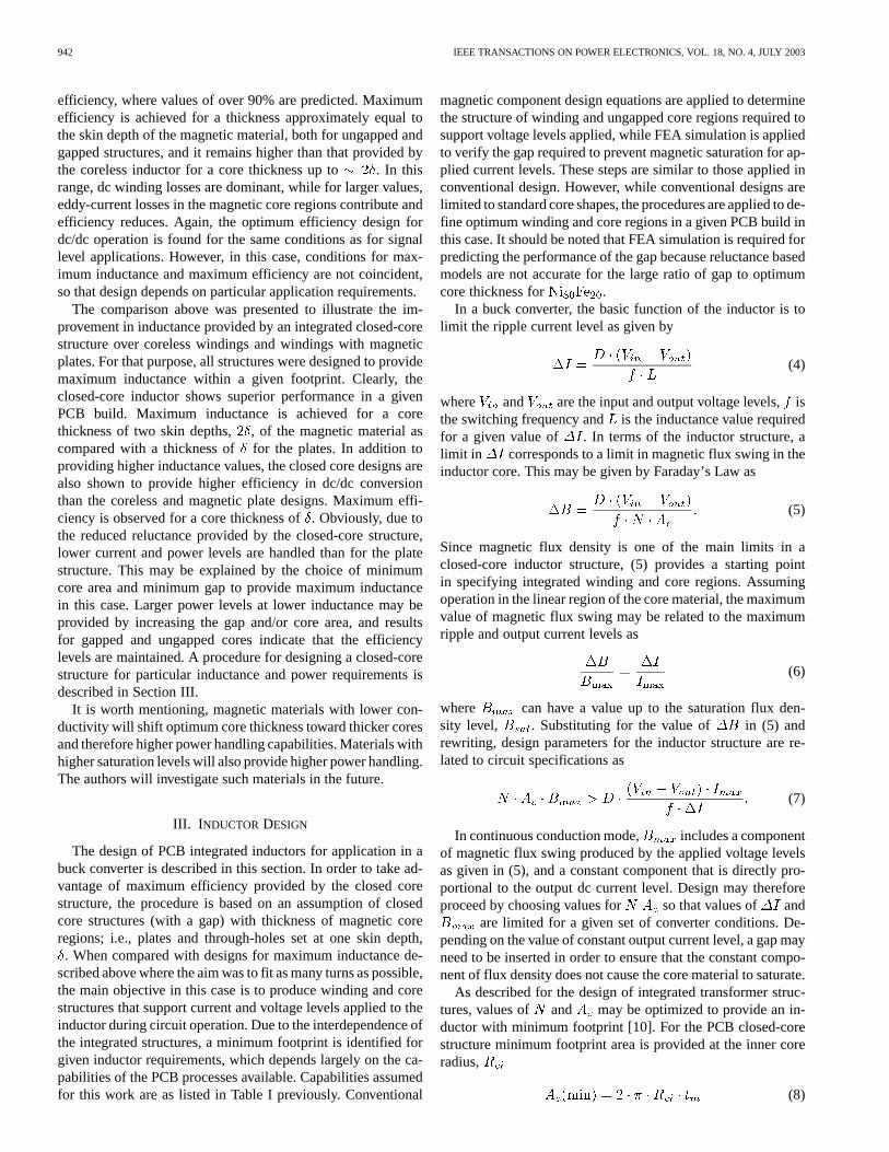
TABLE IIIINDUCTOR STRUCTURE
where is the thickness of electroplated NiFe layers;in thiscase. Replacing in (7), may be expressed in terms of
(9)
Inserting for in the equation for the outer diameter of theinductor structure, with track pitch : , number of windinglayers, and a constant (that relates to the minimum spacingbetween windings and magnetic through-holes)
(10)
where an optimum design with minimum value of may beidentified for given values of , technology parameters andcircuit specifications
(11)the optimum value of is found by differentiating (11) withrespect to , and the corresponding value ofis found in (9).
The procedure is illustrated for the design of an inductor in abuck converter that provides 0.2 A output current and operatesat 1 MHz switching frequency. For a ripple requirement of 30%,an inductance value of 10H is deduced from nominal values ofinput and output voltage using (5). For the technology described,
is chosen as the saturation flux density of permalloy; i.e.,1 T, track pitch is 400 m and there are four winding layerswith two magnetic layers as before. While maximum currentlevels are much lower than 1 A in this case, the same copperthickness of 70 m is assumed so as to maintain winding losseslow. Substituting for in terms of in (10) and minimizingthe outer diameter with respect to , the resulting minimumfootprint structure for 4 winding layers and 5m NiFe thicknessis described in Table III.
Applying the reluctance model to predict the maximum valueof established for 0.25 A in the resulting ungapped core
structure, was calculated as 2.2 T at the inner core radius.Therefore, a gap was needed in the magnetic plates to reduce the
field levels produced. Due to the small thickness of magneticplates, the location of the gap was chosen toward the outer edgeof the inductor where the gap: core area ratio is minimal andtherefore the resulting fringing fields are reduced. A 200mgap was chosen as it is the smallest etchable resolution availableand it was found that two such gaps, i.e., one defined on eachof the magnetic plates was sufficient to prevent saturation in allparts of the core at 0.25 A. As described previously, the windingstructure was manufactured by a PCB manufacturer, and themagnetic plating was completed in house.
IV. M EASUREMENTS
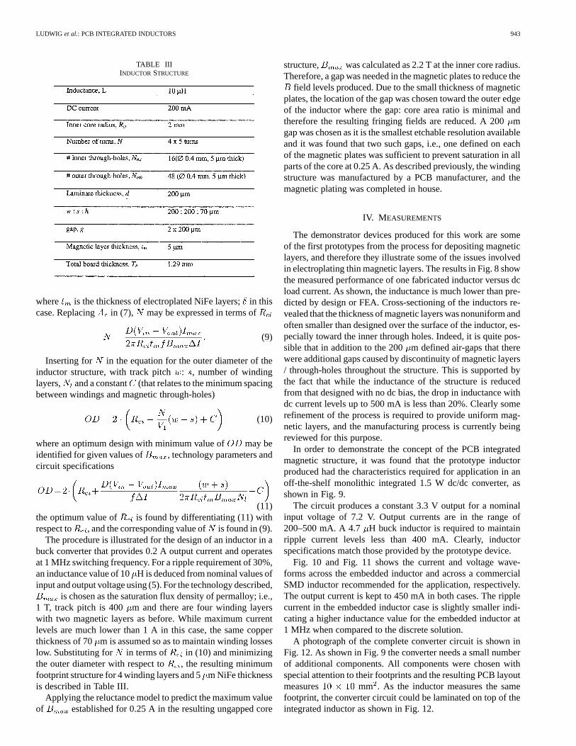
The demonstrator devices produced for this work are someof the first prototypes from the process for depositing magneticlayers, and therefore they illustrate some of the issues involvedin electroplating thin magnetic layers. The results in Fig. 8 showthe measured performance of one fabricated inductor versus dcload current. As shown, the inductance is much lower than pre-dicted by design or FEA. Cross-sectioning of the inductors re-vealed that the thickness of magnetic layers was nonuniform andoften smaller than designed over the surface of the inductor, es-pecially toward the inner through holes. Indeed, it is quite pos-sible that in addition to the 200m defined air-gaps that therewere additional gaps caused by discontinuity of magnetic layers/ through-holes throughout the structure. This is supported bythe fact that while the inductance of the structure is reducedfrom that designed with no dc bias, the drop in inductance withdc current levels up to 500 mA is less than 20%. Clearly somerefinement of the process is required to provide uniform mag-netic layers, and the manufacturing process is currently beingreviewed for this purpose.
In order to demonstrate the concept of the PCB integratedmagnetic structure, it was found that the prototype inductorproduced had the characteristics required for application in anoff-the-shelf monolithic integrated 1.5 W dc/dc converter, asshown in Fig. 9.
The circuit produces a constant 3.3 V output for a nominalinput voltage of 7.2 V. Output currents are in the range of200–500 mA. A 4.7 H buck inductor is required to maintainripple current levels less than 400 mA. Clearly, inductorspecifications match those provided by the prototype device.
Fig. 10 and Fig. 11 shows the current and voltage wave-forms across the embedded inductor and across a commercialSMD inductor recommended for the application, respectively.The output current is kept to 450 mA in both cases. The ripplecurrent in the embedded inductor case is slightly smaller indi-cating a higher inductance value for the embedded inductor at1 MHz when compared to the discrete solution.
A photograph of the complete converter circuit is shown inFig. 12. As shown in Fig. 9 the converter needs a small numberof additional components. All components were chosen withspecial attention to their footprints and the resulting PCB layoutmeasures mm . As the inductor measures the samefootprint, the converter circuit could be laminated on top of theintegrated inductor as shown in Fig. 12.

944 IEEE TRANSACTIONS ON POWER ELECTRONICS, VOL. 18, NO. 4, JULY 2003
Fig. 10. Current and voltage of embedded inductor at an output current of451 mA.
Fig. 11. Current and voltage of discrete inductor at an output current of450 mA.
(a) (b)
Fig. 12. (a) Top view inductor and (b) dc/dc converter on top of inductor.
The efficiency of the converter was measured for two dif-ferent input voltages and results are presented in Fig. 13.
The converter has nearly constant efficiency over a widerange of load and measures ca. 70% for a 7.22 V to 3.3 V and80% for a 5 V to 3.3 V. The output voltage ripple measures50 mV at full load which corresponds to 1.5% output ripple.Therefore the presented integrated solution compares wellin performance and size with the discrete solution using anequivalent compact 1210 SMD inductor.
Fig. 13. Measured converter efficiency of converter at 5 V and 7.2 V input.
V. CONCLUSION
The application of PCB integrated winding and core struc-tures in dc/dc conversion is described for magnetic core regionsthat consist of electroplated NiFe plates and through-holes.Analysis of the performance of different integrated corestructures is presented and compared with that provided by anequivalent air-core device. In this way the limits of eddy-cur-rents and saturation in magnetic core regions are illustrated. Forstructures designed within the same PCB build, the comparisonis made in terms of maximum achievable inductance, powerhandling, power losses and efficiency in a given footprint.Power handling and losses are predicted for a dc biased currentwaveform typical for a buck converter. While the inclusion ofmagnetic plates alone is shown to provide no improvementin circuit performance, the benefits of employing magneticthrough-holes is shown to increase the achievable inductanceby up to 120% and to decrease the dc resistance by 44% ofa coreless inductor of the same footprint. In all cases, thestructures are designed for fabrication in an area of 1 cmofa six-layer PCB, with minimum track pitch of 400m, andminimum through-hole resolution of 400m.
Due to eddy-current effects in conducting magnetic regions,it is shown that advantages of increased inductance and effi-ciency provided by closed-core are limited for values of corethickness less than two skin depths of the magnetic material.Consequently, optimal designs have relatively small core cross-sectional areas when compared with winding dimensions, andpower / current levels that can be supported are limited as a re-sult. For application in dc/dc conversion, a procedure for de-signing PCB integrated inductors to support particular levelsof voltage and current without causing saturation of such thincores is described. Such a procedure has not previously beendescribed for PCB integrated inductors. As a first step, con-ventional magnetic design equations are applied to predict thesmallest PCB area required to accommodate required windingand core regions. Due to the large ratio of gap length to corethickness, FEA simulation is applied to verify the gap lengthneeded to prevent magnetic saturation under dc bias. This way,designs are optimized for maximum power density. Work is on-

LUDWIG et al.: PCB INTEGRATED INDUCTORS 945
going to characterize losses incurred in integrated magnetic re-gions so that designs can be optimized for maximum efficiency.
The procedure is applied to design a 10H/0.2 A buck in-ductor operating at 1 MHz. However, due to initial problemswith uniformity of magnetic layers in the electroplating process,inductance of the structure produced is only 4.7H. Nonethe-less, measurements of inductance as a function of dc currentillustrate that this inductance is maintained for current levelsup to 500 mA. Therefore, in order to illustrate the concept ofusing PCB integrated magnetic components in dc/dc conver-sion, structure is applied in a circuit with a requirement for4.7 H instead of 10 H. When compared with the performanceof the recommended discrete inductor, the PCB integrated in-ductor provides lower ripple current levels and higher efficiency.The overall footprint of the converter was 1 cm, equal to thefootprint of the integrated inductor. In addition to ongoing workin process development and design optimization, magnetic ma-terials with lower conductivity and higher saturation flux den-sity levels will also be investigated. This will lead to dc/dc con-verters with smaller footprints and lower profiles than their dis-crete counterparts, thereby freeing up valuable board space. Inaddition there will be improvements in reliability and costs asthe magnetic components can be built with standard PCB man-ufacturing processes directly into the carrier PCB.
REFERENCES
[1] TPS62102, 1 MHz synchronous PWM dc/dc converter data sheet (2003).http://www.ti.com[Online]
[2] C. R. Sullivan and S. R. Sanders, “Design of microfabricated trans-formers and inductors for high-frequency power conversion,”IEEETrans. Power Electron., vol. 11, pp. 228–238, Mar. 1996.
[3] Y. Katayama, S. Sugahara, H. Nakazawa, and M. Edo, “High power den-sity MHz-switching monolithic dc-dc converter with thin film inductor,”in Proc. 31st IEEE Power Electron. Spec. Conf., Galway, Ireland, June18–23, 2000, pp. 1485–1490.
[4] M. Brunet, T. O’Donnell, J. O’Brien, P. McCloskey, and C. Ó Mathùna,“Design study and fabrication techniques for high power densitymicro-transformers,” inProc. IEEE Appl. Power Electron. Conf. Expo.(APEC), vol. 2, 2001, pp. 1189–1195.
[5] S. O’Reilly, M. Duffy, T. O’Donnell, and S. C. Ó Mathùna, “New inte-grated planar magnetic cores for inductors and transformers fabricatedin MCM-L technology,”Microelectron. Int., vol. 27, no. 1, pp. 25–29,Jan./Feb. 2000.
[6] S. C. Tang, S. Y. R. Hui, and H. S. H. Chung, “A low-profile powerconverter using printed-circuit board (PCB) power transformer withferrite polymer composite,”IEEE Trans. Power Electron., vol. 16, pp.493–498, July 2001.
[7] O. Dezuari, S. E. Gilbert, E. Belloy, and M. A. M. Gijs, “High inductanceplanar transformers,”Sensors Actuators A: Phys., vol. 81, no. 1–3, pp.355–358, Apr., 1 2000.
[8] J. Park and M. Allen, “Low temperature fabrication and characterizationof integrated packaging compatible ferrite core magnetic devices,” inProc. IEEE 12th Appl. Power Electron. Conf., 1997, pp. 362–367.
[9] M. Duffy, S. O Reilly, T. O Donnell, P. Friesen, P. McCloskey, and S.C. Ó Mathùna, “MCM-L integrated transformers for low power appli-cations,” inProc. IEEE Power Electron. Spec. Conf., PESC 2000, vol.1, pp. 302–307.
[10] MIL-STD-275E, NOTICE 1, July 8, 1986.[11] W. G. Hurley and M. C. Duffy, “Calculation of self- and mutual imped-
ances in planar sandwich inductors,”IEEE Trans. Magn., vol. 33, pp.2282–2290, May 1997.
[12] Maxwell 2-D, , Ansoft Corporation, 2003.[13] M. Ludwig, M. Duffy, T. O’Donnell, and S. C. Ó Mathùna, “PCB inte-
grated Inductors for Low Power dc/dc Converter,” inProc. 17th Annu.IEEE Appl. Power Electron. Conf. Expo. (APEC’02), vol. 1, Dallas, TX,2002, pp. 319–325.
[14] W. H. Hayt, Engineering Electromagnetics, 4th ed. New York: Mc-Graw-Hill.
Matthias Ludwig (S’91) was born in Fulda,Germany, in 1971. He received the M.Sc. degreein electrical engineering from Darmstadt Universityof Technology, Germany, in 1998 and is currentlypursuing the Ph.D. degree in microelectronics atthe Energy Processing for ICT Team, NationalMicroelectronics Research Centre, UniversityCollege, Cork, Ireland.
His research interests are in the field of designand modeling of planar and integrated magnetics forpower conversion and switch mode power supplies.
Maeve Duffy (M’94) was born in Monaghan,Ireland. She received the B.E. degree (with honors)in electronic engineering and the Ph.D. degree inplanar magnetics from the National University ofIreland, Galway (NUIG), Ireland, in 1992 and 1997,respectively.
She was a Research Officer with PEI Technolo-gies, National Microelectronics Research Centre,Cork, Ireland, from 1997 to 2001. She is currentlya Lecturer with the Department of ElectronicEngineering, NUIG. Her main research interests are
in modeling and design of magnetic components, including planar magneticsand magnetic sensors.
Terence O’Donnell(M’97) received the B.E. degreein electrical engineering from University College,Dublin, Ireland, in 1990 and the Ph.D. degree fromthe National University of Ireland in 1996.
He is currently a Senior Research Officier with theEnergy Processing for ICT Team, National Micro-electronics Research Centre, Cork, Ireland. His mainresearch area is in the design and modeling of planarand integrated magnetics, for applications in powerconversion, datacomms, telecomms, and MEMS.
Paul McCloskeyreceived the B.Sc. degree in chem-ical engineering from Queens University, Belfast,U.K., in 1981 and the M.Sc. degree in energy studiesand the M.Sc. degree in microelectronics fromthe University of Ulster, U.K., in 1984 and 1991,respectively.
He has worked for 14 years in electronics man-ufacturing and has for the past four years been theleader of the “Energy Processing for ICT” Team, Na-tional Microelectronics Research Centre, UniversityCollege, Cork, Ireland. The team’s research interests
are in integrated magnetics for power conversion and power transfer and powerelectronic packaging.
Seán Cian Ó Mathúna received the B.E.,M.Eng.Sc., and Ph.D. degrees from the NationalUniversity of Ireland, in 1981, 1984, and 1994,respectively.
From 1982 to 1993, he was instrumental inestablishing the Interconnection and PackagingGroup, National Microelectronics Research Centre(NMRC), University College Cork, Ireland, wherehe held the position of Senior Research Scientist.In 1993, he joined PEI Technologies, NMRC,
as Technical/Commercial Director, where he was responsible for powerpackaging, planar/integrated magnetics, and product qualification. In 1997, herejoined NMRC as Group Director with responsibility for Microsystems. In1999, he was appointed as Assistant Director for NMRC with responsibilityfor microelectronics integration with research themes in ambient electronics,biomiedical microsystems, and energy processing for ICT.


