Embed Size (px)
Citation preview

PCB Design Introduction and Demo
February 16th 2016
Presented by: Benjamin Rhoades

Agenda
• What is a Printed Circuit Board (PCB)?
• Why do Embedded Engineers need them?
• Basic Terminology Specific to PCBs
• Design Consideration / Constraints
- Size
- Cost
- Power Requirements
• PCB Soldering Techniques
• Pitfalls in PCB Design
• Demo Time!
• Additional Resources (How to get a board made)
• References

What is a Printed Circuit Board (PCB)?
• A printed Circuit Board or PCB is simply a
copper etched board that contains traces to
varies components

Why Do Embedded Engineers Need a PCB?
• As an embedded engineer you will eventually be
“embedded” your designed device into its final
location.
• Examples include:
− Bridge Monitoring
− Cell Phone

Why Do Embedded Engineers Need a PCB?
Smaller Manufacturing
makes for smaller
devices

Why Do Embedded Engineers Need a PCB?
Making
Items
smaller!

Terminology (Layers)
• Many boards are multilayer board to
accommodate all the components needed for
the board to be compact and function in its
intended environment
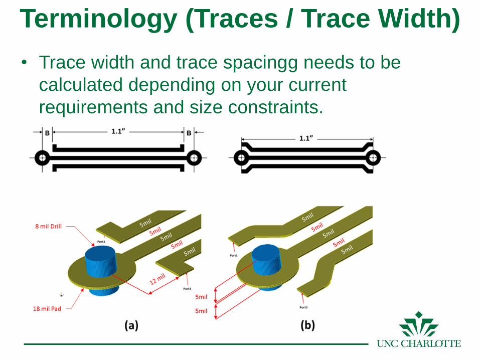
Terminology (Traces / Trace Width)
• Trace width and trace spacingg needs to be
calculated depending on your current
requirements and size constraints.

Terminology (Part Footprints)
• All THT and SMT parts have
an accosted footprint with
the device. Most
manufactures / distributors
will offer a large variety of
package sizes for each part.

Terminology (Part Package Size)
• When designing a PCB
with tight size constraints
you will need to consider
the different package size
for your parts that you will
be using
• *NOTE* that the smaller
the package size the
harder it is to solder by
hand (sometimes
impossible )

Terminology (Through Hole, Surface Mount )
• There are two basic component types
− Through Hole
− Surface Mount
THT(Through Hole Technology)
SMT(Surface Mount Technology)
• Depending on your
application you may
use only SMT, only
THT or a combo of
the two

Terminology (Silkscreen & Soldermask)
• To make a board that can
be assembled easily you
need to have a
silkscreen layer to
indicate the placement of
your parts A BSoldermask expansion (a) and silkscreen (b)
*Note* having a
naming convention
for naming parts is
crucial in a large
PCB design

Terminology (Vias)
• Vias are used when you cannot make another
trace and thus you need to use a via (we will be
using one in the example board in our later
demo)

Terminology ( Headers / Connectors)
• For most applications you will need to interface
your designed PCB with another PCB (called a
Daughter Board) or some other peripheral
device.
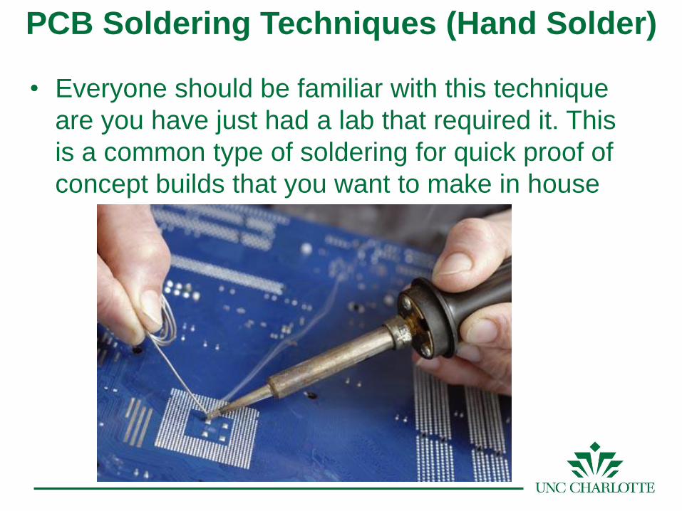
PCB Soldering Techniques (Hand Solder)
• Everyone should be familiar with this technique
are you have just had a lab that required it. This
is a common type of soldering for quick proof of
concept builds that you want to make in house
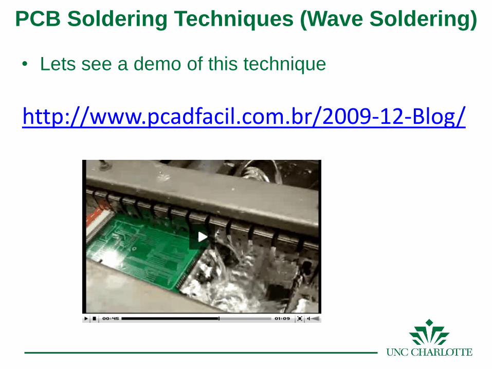
PCB Soldering Techniques (Wave Soldering)
• Lets see a demo of this technique
http://www.pcadfacil.com.br/2009-12-Blog/

PCB Soldering Techniques (Etching)
• A good technique for quick prototyping for proof of
concept
• Downfalls is that you have to drill all holes and vias by
hand
• Lets watch a quick video on this technique
https://www.youtube.com/watch?v=N3DGbwVXyN8

Design Considerations (Size)
• The size of the PCB will depend on your end
application (Will it be fully embedded?)

Design Constraint (Power)
• After you have designed a PCB you need to consider
how you will power your end device.
• Will it be connected to “The Grid” aka infite power or will
you be placing the device in a remote location (i.e. finite
power source aka A battery)

Design Consideration (RF shielding)
For high frequency applications
you will need to employ a
technique called shielding (and
co-planer waveguides shown
here with the SMA connector)Co-Planer Waveguides

Pitfalls in PCB Design (Units)
• Ensuring that you are in
the correct units is
imperative in PCB design.
• All manufacturers use
different standards for their
parts
• Note this will also be
designated in the
mechanical drawing of the
datasheet of any part that
you desire to use

Pitfalls in PCB Design
(Part Ordering / Backorder)
• To build a board you need to make sure the
parts are available (not on backorder )

15.24 [0.6]
2.54 [0.1]
7.620000
Q: Can you spot the problem?
A: The default footprint does
not fit the desired part… thus
we must make a custom part!
Pitfalls in PCB Design (Custom Footprints)

Design Constraint (Serviceability)
• Will you need to ever service the PCB that you
have designed. (This decision is usually left up
to the end user or the customer)
A Commodore 64 Logic Board from the late 1980’s

DEMO TIME!

Additional Resources
• EEVBlog (Wild Aussie man but very good content!)
Here are three good videos he has on PCB design and
manufacturing:
Part # 1 Part # 2 Part # 3 His YouTube Channel
• A really good “Manual” on PCB design, terminology, and
all around best practices… Here is the Link
• Here are some of the websites to the local manufactures
that was discussed earlier in the presentation…
• M&M Technologies (Indian Trail, NC)
• GMI Manufacturing (Mooresville, NC)
• Micro Circuits Diversified (Salisbury, NC)

ReferencesPictures
1. http://bytesdaily.blogspot.com/2015/07/funny-friday.html
2. https://upload.wikimedia.org/wikipedia/commons/8/86/Photo-SMDcapacitors.jpg
3. http://store.curiousinventor.com/guides/Surface_Mount_Soldering
4. https://c2.staticflickr.com/6/5172/5477287563_00fe802818_b.jpg
5. http://www.e2save.com/content/Smartphones/inside-out-phones/img/screen-good-foundations-old.png
6. http://www.soyacincau.com/wp-content/uploads/2011/11/111130-samsung-galaxy-nexus-teardown.jpg
7. http://img.wonderhowto.com/img/00/66/63440148210407/0/from-backpack-transceiver-smartphone-visual-history-mobile-
phone.w654.jpg
8. http://cdn.gsmarena.com/pics/14/08/samsung-galaxy-s5-mini-hands-on/big.jpg
9. http://hollandshielding.com/content/1500/1500_Large_clip_on_active_2.gif
10. http://www.comsol.com/model/image/15681/big.png
11. http://www.deepcoat.com/images/form-shield-big.jpg
12. http://www.pcb.electrosoft-engineering.com/04-articles-custom-system-design-and-pcb/01-printed-circuit-board-concepts/printed-
circuit-board-pcb-concepts.html
13. http://www.robotroom.com/Laser-Sensor/Laser-Controlled-Circuit-On-Solderless-Breadboard.jpg
14. https://sites.google.com/site/doktormusic/swept-sounds-solder-side.jpg
15. http://www.instructables.com/files/deriv/FH0/02K7/HHMHZKUR/FH002K7HHMHZKUR.LARGE.jpg
16. http://chibi-sakura.org/images/smd_chart_v01.png
17. http://connectorterminal.en.ecplaza.net/14.jpg
18. http://gct.co/pcb-board-to-board/pcb-connector-overview/images%5Cpcb-connector-overview-2.png
19. https://bertsimonovich.files.wordpress.com/2013/04/image66.png
20. https://learn.sparkfun.com/tutorials/pcb-basics/whats-a-pcb
21. http://www.electronicsandyou.com/blog/wp-content/uploads/2013/06/Hand-Soldering.jpg
22. http://smallbotics.solarbotics.net/index_files/pcb%20etch5.jpg
23. http://1010.co.uk/images/pcb3.jpg
24. http://previews.123rf.com/images/audriusmerfeldas/audriusmerfeldas1506/audriusmerfeldas150600250/41904118-Abstract-
photography-of-different-various-PCBs-Stock-Photo.jpg
25. http://www.hackmelbourne.org/wiki/_media/doc:orders:digikey:addtocart.png
26. http://c8.alamy.com/comp/EJKGBM/pile-of-various-batteries-EJKGBM.jpg