Embed Size (px)
Citation preview

1. General description
The PCA9547 is an octal bidirectional translating multiplexer controlled by the I2C-bus.The SCL/SDA upstream pair fans out to eight downstream pairs, or channels. Only oneSCx/SDx channel can be selected at a time, determined by the contents of theprogrammable control register. The device powers up with Channel 0 connected, allowingimmediate communication between the master and downstream devices on that channel.
An active LOW reset input allows the PCA9547 to recover from a situation where one ofthe downstream I2C-buses is stuck in a LOW state. Pulling the RESET pin LOW resets theI2C-bus state machine causing all the channels to be deselected, except Channel 0 sothat the master can regain control of the bus.
The pass gates of the multiplexers are constructed such that the VDD pin can be used tolimit the maximum high voltage which will be passed by the PCA9547. This allows the useof different bus voltages on each pair, so that 1.8 V, 2.5 V, or 3.3 V parts can communicatewith 5 V parts without any additional protection. External pull-up resistors pull the bus upto the desired voltage level for each channel. All I/O pins are 5 V tolerant.
2. Features
n 1-of-8 bidirectional translating multiplexer
n I2C-bus interface logic; compatible with SMBus standards
n Active LOW RESET input
n 3 address pins allowing up to 8 devices on the I2C-bus
n Channel selection via I2C-bus, one channel at a time
n Power-up with all channels deselected except Channel 0 which is connected
n Low Ron multiplexers
n Allows voltage level translation between 1.8 V, 2.5 V, 3.3 V and 5 V buses
n No glitch on power-up
n Supports hot insertion
n Low standby current
n Operating power supply voltage range of 2.3 V to 5.5 V
n 5 V tolerant inputs
n 0 Hz to 400 kHz clock frequency
n ESD protection exceeds 2000 V HBM per JESD22-A114, 200 V MM perJESD22-A115, and 1000 V CDM per JESD22-C101
n Latch-up testing is done to JEDEC Standard JESD78 which exceeds 100 mA
n Packages offered: SO24, TSSOP24, HVQFN24
PCA95478-channel I 2C-bus multiplexer with resetRev. 02 — 12 September 2006 Product data sheet

Philips Semiconductors PCA95478-channel I 2C-bus multiplexer with reset
3. Ordering information
3.1 Ordering options
Table 1. Ordering information
Type number Package
Name Description Version
PCA9547D SO24 plastic small outline package; 24 leads;body width 7.5 mm
SOT137-1
PCA9547PW TSSOP24 plastic thin shrink small outline package; 24 leads;body width 4.4 mm
SOT355-1
PCA9547BS HVQFN24 plastic thermal enhanced very thin quad flat package;no leads; 24 terminals; body 4 × 4 × 0.85 mm
SOT616-1
Table 2. Ordering options
Type number Topside mark Temperature range
PCA9547D PCA9547D Tamb = −40 °C to +85 °C
PCA9547PW PCA9547 Tamb = −40 °C to +85 °C
PCA9547BS 9547 Tamb = −40 °C to +85 °C
PCA9547_2 © Koninklijke Philips Electronics N.V. 2006. All rights reserved.
Product data sheet Rev. 02 — 12 September 2006 2 of 26

Philips Semiconductors PCA95478-channel I 2C-bus multiplexer with reset
4. Block diagram
Fig 1. Block diagram of PCA9547
SWITCH CONTROL LOGIC
PCA9547
RESETCIRCUIT
002aaa961
SC0
SC1
SC2
SC3
SC4
SC5
SC6
SC7
SD0
SD1
SD2
SD3
SD4
SD5
SD6
SD7
VSS
VDD
RESET
I2C-BUSCONTROL
INPUTFILTER
SCL
SDA
A0
A1
A2
PCA9547_2 © Koninklijke Philips Electronics N.V. 2006. All rights reserved.
Product data sheet Rev. 02 — 12 September 2006 3 of 26

Philips Semiconductors PCA95478-channel I 2C-bus multiplexer with reset
5. Pinning information
5.1 Pinning
Fig 2. Pin configuration for SO24 Fig 3. Pin configuration for TSSOP24
Fig 4. Pin configuration for HVQFN24 (transparent top view)
PCA9547D
A0 VDD
A1 SDA
RESET SCL
SD0 A2
SC0 SC7
SD1 SD7
SC1 SC6
SD2 SD6
SC2 SC5
SD3 SD5
SC3 SC4
VSS SD4
002aaa958
1
2
3
4
5
6
7
8
9
10
11
12
14
13
16
15
18
17
20
19
22
21
24
23
PCA9547PW
A0 VDD
A1 SDA
RESET SCL
SD0 A2
SC0 SC7
SD1 SD7
SC1 SC6
SD2 SD6
SC2 SC5
SD3 SD5
SC3 SC4
VSS SD4
002aaa959
1
2
3
4
5
6
7
8
9
10
11
12
14
13
16
15
18
17
20
19
22
21
24
23
002aaa960
PCA9547BS
Transparent top view
SC5
SD2
SC2
SD6
SC1 SC6
SD1 SD7
SC0 SC7
SD0 A2
SD
3
SC
3
VS
S
SD
4
SC
4
SD
5
RE
SE
T
A1
A0
VD
D
SD
A
SC
L
terminal 1index area
6 13
5 14
4 15
3 16
2 17
1 18
7 8 9 10 11 12
24 23 22 21 20 19
PCA9547_2 © Koninklijke Philips Electronics N.V. 2006. All rights reserved.
Product data sheet Rev. 02 — 12 September 2006 4 of 26

Philips Semiconductors PCA95478-channel I 2C-bus multiplexer with reset
5.2 Pin description
[1] HVQFN package die supply ground is connected to both the VSS pin and the exposed center pad. The VSSpin must be connected to supply ground for proper device operation. For enhanced thermal, electrical, andboard-level performance, the exposed pad needs to be soldered to the board using a correspondingthermal pad on the board, and for proper heat conduction through the board thermal vias need to beincorporated in the PCB in the thermal pad region.
Table 3. Pin description
Symbol Pin Description
SO, TSSOP HVQFN
A0 1 22 address input 0
A1 2 23 address input 1
RESET 3 24 active LOW reset input
SD0 4 1 serial data output 0
SC0 5 2 serial clock output 0
SD1 6 3 serial data output 1
SC1 7 4 serial clock output 1
SD2 8 5 serial data output 2
SC2 9 6 serial clock output 2
SD3 10 7 serial data output 3
SC3 11 8 serial clock output 3
VSS 12 9[1] supply ground
SD4 13 10 serial data output 4
SC4 14 11 serial clock output 4
SD5 15 12 serial data output 5
SC5 16 13 serial clock output 5
SD6 17 14 serial data output 6
SC6 18 15 serial clock output 6
SD7 19 16 serial data output 7
SC7 20 17 serial clock output 7
A2 21 18 address input 2
SCL 22 19 serial clock line
SDA 23 20 serial data line
VDD 24 21 supply voltage
PCA9547_2 © Koninklijke Philips Electronics N.V. 2006. All rights reserved.
Product data sheet Rev. 02 — 12 September 2006 5 of 26

Philips Semiconductors PCA95478-channel I 2C-bus multiplexer with reset
6. Functional description
6.1 Device addressingFollowing a START condition, the bus master must output the address of the slave it isaccessing. The address of the PCA9547 is shown in Figure 5. To conserve power, nointernal pull-up resistors are incorporated on the hardware selectable address pins andthey must be pulled HIGH or LOW.
The last bit of the slave address defines the operation to be performed. When set tologic 1 a read is selected, while a logic 0 selects a write operation.
6.2 Control registerFollowing the successful acknowledgement of the slave address, the bus master will senda byte to the PCA9547, which will be stored in the Control register. If multiple bytes arereceived by the PCA9547, it will save the last byte received. This register can be writtenand read via the I2C-bus.
6.2.1 Control register definition
A SCx/SDx downstream pair, or channel, is selected by the contents of the controlregister. This register is written after the PCA9547 has been addressed. The 4 LSBs ofthe control byte are used to determine which channel is to be selected. When a channel isselected, the channel will become active after a STOP condition has been placed on theI2C-bus. This ensures that all SCx/SDx lines will be in a HIGH state when the channel ismade active, so that no false conditions are generated at the time of connection.
Fig 5. Slave address
002aaa962
1 1 1 0 A2 A1 A0 R/W
fixed hardwareselectable
Fig 6. Control register
002aaa963
X X X X B3 B2 B1 B0
channel selection bits(read/write)
7 6 5 4 3 2 1 0
enable bit
PCA9547_2 © Koninklijke Philips Electronics N.V. 2006. All rights reserved.
Product data sheet Rev. 02 — 12 September 2006 6 of 26
Philips Semiconductors PCA95478-channel I 2C-bus multiplexer with reset
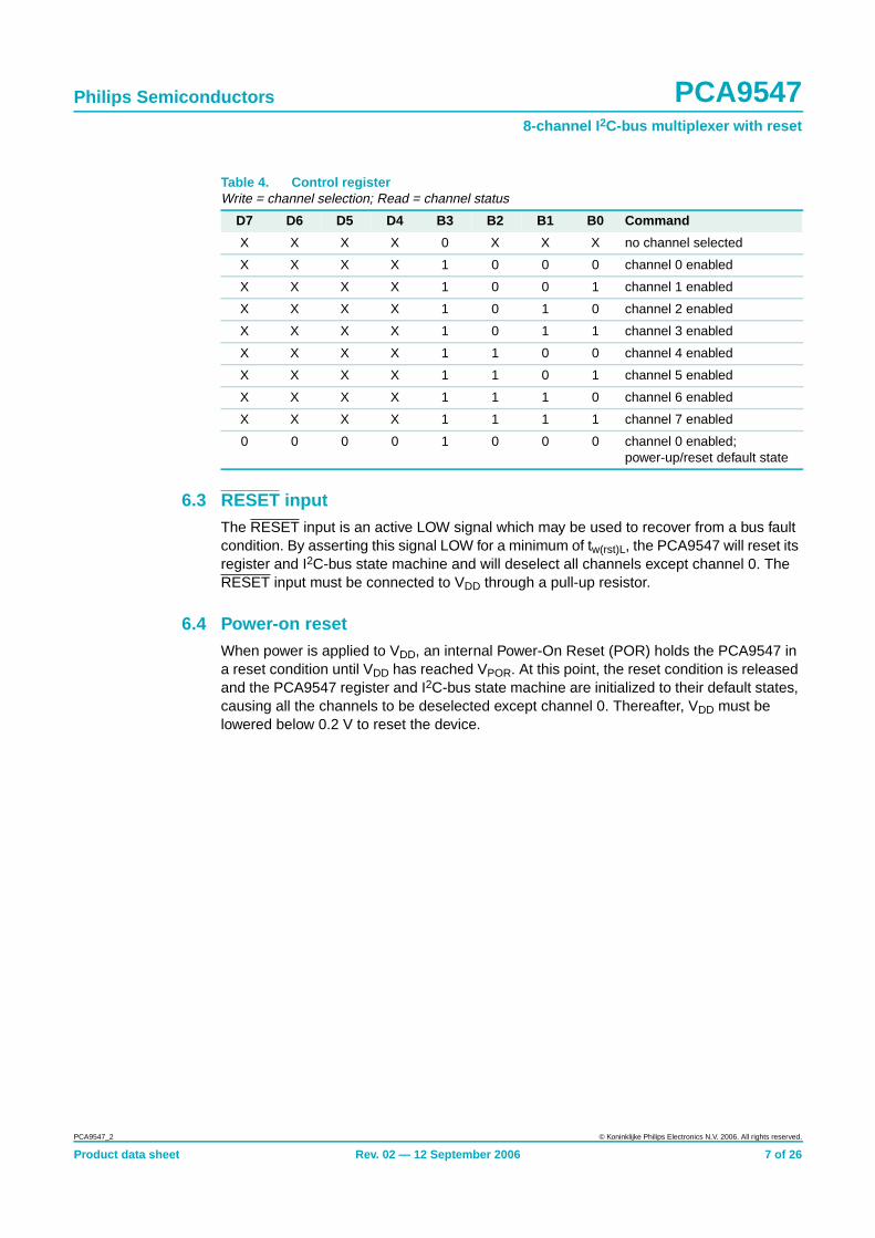
6.3 RESET inputThe RESET input is an active LOW signal which may be used to recover from a bus faultcondition. By asserting this signal LOW for a minimum of tw(rst)L, the PCA9547 will reset itsregister and I2C-bus state machine and will deselect all channels except channel 0. TheRESET input must be connected to VDD through a pull-up resistor.
6.4 Power-on resetWhen power is applied to VDD, an internal Power-On Reset (POR) holds the PCA9547 ina reset condition until VDD has reached VPOR. At this point, the reset condition is releasedand the PCA9547 register and I2C-bus state machine are initialized to their default states,causing all the channels to be deselected except channel 0. Thereafter, VDD must belowered below 0.2 V to reset the device.
Table 4. Control registerWrite = channel selection; Read = channel status
D7 D6 D5 D4 B3 B2 B1 B0 Command
X X X X 0 X X X no channel selected
X X X X 1 0 0 0 channel 0 enabled
X X X X 1 0 0 1 channel 1 enabled
X X X X 1 0 1 0 channel 2 enabled
X X X X 1 0 1 1 channel 3 enabled
X X X X 1 1 0 0 channel 4 enabled
X X X X 1 1 0 1 channel 5 enabled
X X X X 1 1 1 0 channel 6 enabled
X X X X 1 1 1 1 channel 7 enabled
0 0 0 0 1 0 0 0 channel 0 enabled;power-up/reset default state
PCA9547_2 © Koninklijke Philips Electronics N.V. 2006. All rights reserved.
Product data sheet Rev. 02 — 12 September 2006 7 of 26

Philips Semiconductors PCA95478-channel I 2C-bus multiplexer with reset
6.5 Voltage translationThe pass gate transistors of the PCA9547 are constructed such that the VDD voltage canbe used to limit the maximum voltage that will be passed from one I2C-bus to another.
Figure 7 shows the voltage characteristics of the pass gate transistors (note that thePCA9547 is only tested at the points specified in Section 10 “Static characteristics” of thisdata sheet). In order for the PCA9547 to act as a voltage translator, the Vo(mux) voltageshould be equal to, or lower than the lowest bus voltage. For example, if the main bus wasrunning at 5 V, and the downstream buses were 3.3 V and 2.7 V, then Vo(mux) should beequal to or below 2.7 V to effectively clamp the downstream bus voltages. Looking atFigure 7, we see that Vo(mux)(max) will be at 2.7 V when the PCA9547 supply voltage is3.5 V or lower so the PCA9547 supply voltage could be set to 3.3 V. Pull-up resistors canthen be used to bring the bus voltages to their appropriate levels (see Figure 14).
More information can be found in Application Note AN262, PCA954X family of I2C/SMBusmultiplexers and switches.
(1) maximum
(2) typical
(3) minimum
Fig 7. Pass gate voltage as a function of supply voltage
VDD (V)2.0 5.54.53.0 4.0
002aab802
3.0
2.0
4.0
5.0
Vo(mux)(V)
1.03.5 5.02.5
(1)
(2)
(3)
PCA9547_2 © Koninklijke Philips Electronics N.V. 2006. All rights reserved.
Product data sheet Rev. 02 — 12 September 2006 8 of 26

Philips Semiconductors PCA95478-channel I 2C-bus multiplexer with reset
7. Characteristics of the I 2C-bus
The I2C-bus is for 2-way, 2-line communication between different ICs or modules. The twolines are a serial data line (SDA) and a serial clock line (SCL). Both lines must beconnected to a positive supply via a pull-up resistor when connected to the output stagesof a device. Data transfer may be initiated only when the bus is not busy.
7.1 Bit transferOne data bit is transferred during each clock pulse. The data on the SDA line must remainstable during the HIGH period of the clock pulse as changes in the data line at this timewill be interpreted as control signals (see Figure 8).
7.1.1 START and STOP conditions
Both data and clock lines remain HIGH when the bus is not busy. A HIGH-to-LOWtransition of the data line while the clock is HIGH is defined as the START condition (S). ALOW-to-HIGH transition of the data line while the clock is HIGH is defined as the STOPcondition (P) (seeFigure 9.)
Fig 8. Bit transfer
mba607
data linestable;
data valid
changeof dataallowed
SDA
SCL
Fig 9. Definition of START and STOP conditions
mba608
SDA
SCLP
STOP condition
SDA
SCLS
START condition
PCA9547_2 © Koninklijke Philips Electronics N.V. 2006. All rights reserved.
Product data sheet Rev. 02 — 12 September 2006 9 of 26

Philips Semiconductors PCA95478-channel I 2C-bus multiplexer with reset
7.2 System configurationA device generating a message is a ‘transmitter’; a device receiving is the ‘receiver’. Thedevice that controls the message is the ‘master’ and the devices which are controlled bythe master are the ‘slaves’ (see Figure 10).
7.3 AcknowledgeThe number of data bytes transferred between the START and the STOP conditions fromtransmitter to receiver is not limited. Each byte of eight bits is followed by oneacknowledge bit. The acknowledge bit is a HIGH level put on the bus by the transmitter,whereas the master generates an extra acknowledge related clock pulse.
A slave receiver which is addressed must generate an acknowledge after the reception ofeach byte. Also a master must generate an acknowledge after the reception of each bytethat has been clocked out of the slave transmitter. The device that acknowledges has topull down the SDA line during the acknowledge clock pulse, so that the SDA line is stableLOW during the HIGH period of the acknowledge related clock pulse; setup and holdtimes must be taken into account.
A master receiver must signal an end of data to the transmitter by not generating anacknowledge on the last byte that has been clocked out of the slave. In this event, thetransmitter must leave the data line HIGH to enable the master to generate a STOPcondition.
Fig 10. System configuration
002aaa966
MASTERTRANSMITTER/
RECEIVER
SLAVERECEIVER
SLAVETRANSMITTER/
RECEIVER
MASTERTRANSMITTER
MASTERTRANSMITTER/
RECEIVER
SDA
SCL
I2C-BUSMULTIPLEXER
SLAVE
Fig 11. Acknowledgement on the I 2C-bus
002aaa987
S
STARTcondition
9821
clock pulse foracknowledgement
not acknowledge
acknowledge
data outputby transmitter
data outputby receiver
SCL from master
PCA9547_2 © Koninklijke Philips Electronics N.V. 2006. All rights reserved.
Product data sheet Rev. 02 — 12 September 2006 10 of 26

Philips Semiconductors PCA95478-channel I 2C-bus multiplexer with reset
7.4 Bus transactionsData is transmitted to the PCA9547 control register using the Write mode as shown inFigure 12.
Data is read from PCA9547 using the Read mode as shown in Figure 13.
Fig 12. Write control register
Fig 13. Read control register
002aaa988
X X X X B3 B2 B1 B01 1 0 A2 A1 A0 0 AS 1 A P
slave address
START condition R/W acknowledgefrom slave
acknowledgefrom slave
control register
SDA
STOP condition
002aaa989
X X X X B3 B2 B1 B01 1 0 A2 A1 A0 1 AS 1 NA P
slave address
START condition R/W acknowledgefrom slave
no acknowledgefrom master
control register
SDA
STOP condition
last byte
PCA9547_2 © Koninklijke Philips Electronics N.V. 2006. All rights reserved.
Product data sheet Rev. 02 — 12 September 2006 11 of 26

Philips Semiconductors PCA95478-channel I 2C-bus multiplexer with reset
8. Application design-in information
Fig 14. Typical application
PCA9547
SD0
SC0
SD1
SC1
A1
A0
VSS
SDA
SCL
RESET
VDD = 3.3 VVDD = 2.7 V to 5.5 V
I2C-bus/SMBusmaster
002aaa965
SDA
SCLchannel 0
channel 1
SD2
SC2channel 2
SD3
SC3channel 3
A2
SD4
SC4
V = 2.7 V to 5.5 V
SD5
SC5
channel 4
channel 5
SD6
SC6channel 6
V = 2.7 V to 5.5 V
SD7
SC7channel 7
V = 2.7 V to 5.5 V
V = 2.7 V to 5.5 V
V = 2.7 V to 5.5 V
V = 2.7 V to 5.5 V
V = 2.7 V to 5.5 V
V = 2.7 V to 5.5 V
PCA9547_2 © Koninklijke Philips Electronics N.V. 2006. All rights reserved.
Product data sheet Rev. 02 — 12 September 2006 12 of 26

Philips Semiconductors PCA95478-channel I 2C-bus multiplexer with reset
9. Limiting values
[1] The performance capability of a high-performance integrated circuit in conjunction with its thermalenvironment can create junction temperatures which are detrimental to reliability. The maximum junctiontemperature of this integrated circuit should not exceed 150 °C.
Table 5. Limiting valuesIn accordance with the Absolute Maximum Rating System (IEC 60134).[1]
Symbol Parameter Conditions Min Max Unit
VDD supply voltage −0.5 +7.0 V
VI input voltage −0.5 +7.0 V
II input current −20 +20 mA
IO output current −25 +25 mA
IDD supply current −100 +100 mA
ISS ground supply current −100 +100 mA
Ptot total power dissipation - 400 mW
Tstg storage temperature −60 +150 °C
Tamb ambient temperature −40 +85 °C
PCA9547_2 © Koninklijke Philips Electronics N.V. 2006. All rights reserved.
Product data sheet Rev. 02 — 12 September 2006 13 of 26

Philips Semiconductors PCA95478-channel I 2C-bus multiplexer with reset
10. Static characteristics
[1] For operation between published voltage ranges, refer to the worst-case parameter in both ranges.
[2] VDD must be lowered to 0.2 V in order to reset part.
Table 6. Static characteristicsVDD = 2.3 V to 3.6 V; VSS = 0 V; Tamb = −40 °C to +85 °C; unless otherwise specified.See Table 7 on page 15 for VDD = 4.5 V to 5.5 V.[1]
Symbol Parameter Conditions Min Typ Max Unit
Supply
VDD supply voltage 2.3 - 3.6 V
IDD supply current operating mode; VDD = 3.6 V; no load;VI = VDD or VSS; fSCL = 100 kHz
- 20 50 µA
Istb standby current Standby mode; VDD = 3.6 V; no load;VI = VDD or VSS
- 0.1 2 µA
VPOR power-on reset voltage no load; VI = VDD or VSS[2] - 1.6 2.1 V
Input SCL; input/output SDA
VIL LOW-level input voltage −0.5 - +0.3VDD V
VIH HIGH-level input voltage 0.7VDD - 6 V
IOL LOW-level output current VOL = 0.4 V 3 - - mA
VOL = 0.6 V 6 - - mA
IL leakage current VI = VDD or VSS −1 - +1 µA
Ci input capacitance VI = VSS - 14 19 pF
Select inputs A0, A1, A2, RESET
VIL LOW-level input voltage −0.5 - +0.3VDD V
VIH HIGH-level input voltage 0.7VDD - VDD + 0.5 V
ILI input leakage current pin at VDD or VSS −1 - +1 µA
Ci input capacitance VI = VSS - 2 5 pF
Pass gate
Ron ON-state resistance multiplexer; VDD = 3.6 V; VO = 0.4 V;IO = 15 mA
5 11 30 Ω
multiplexer; VDD = 2.3 V to 2.7 V;VO = 0.4 V; IO = 10 mA
7 16 55 Ω
Vo(mux) multiplexer output voltage Vi(mux) = VDD = 3.3 V; Io(mux) = −100 µA - 1.9 - V
Vi(mux) = VDD = 3.0 V to 3.6 V;Io(mux) = −100 µA
1.6 - 2.8 V
Vo(mux) = VDD = 2.5 V;Io(mux) = −100 µA
- 1.5 - V
Vo(mux) = VDD = 2.3 V to 2.7 V;Io(mux) = −100 µA
0.9 - 2.0 V
IL leakage current VI = VDD or VSS −1 - +1 µA
Cio input/output capacitance VI = VSS - 3 5 pF
PCA9547_2 © Koninklijke Philips Electronics N.V. 2006. All rights reserved.
Product data sheet Rev. 02 — 12 September 2006 14 of 26

Philips Semiconductors PCA95478-channel I 2C-bus multiplexer with reset
[1] For operation between published voltage ranges, refer to the worst-case parameter in both ranges.
[2] VDD must be lowered to 0.2 V in order to reset part.
Table 7. Static characteristicsVDD = 4.5 V to 5.5 V; VSS = 0 V; Tamb = −40 °C to +85 °C; unless otherwise specified.See Table 6 on page 14 for VDD = 2.3 V to 3.6 V.[1]
Symbol Parameter Conditions Min Typ Max Unit
Supply
VDD supply voltage 4.5 - 5.5 V
IDD supply current operating mode; VDD = 5.5 V;no load; VI = VDD or VSS;fSCL = 100 kHz
- 65 100 µA
Istb standby current Standby mode; VDD = 5.5 V;no load; VI = VDD or VSS
- 0.6 2 µA
VPOR power-on reset voltage no load; VI = VDD or VSS[2] - 1.7 2.1 V
Input SCL; input/output SDA
VIL LOW-level input voltage −0.5 - +0.3VDD V
VIH HIGH-level input voltage 0.7VDD - 6 V
IOL LOW-level output current VOL = 0.4 V 3 - - mA
VOL = 0.6 V 6 - - mA
IIL LOW-level input current VI = VSS 1 - 1 µA
IIH HIGH-level input current VI = VSS 1 - 1 µA
Ci input capacitance VI = VSS - 14 19 pF
Select inputs A0, A1, A2, RESET
VIL LOW-level input voltage −0.5 - +0.3VDD V
VIH HIGH-level input voltage 0.7VDD - VDD + 0.5 V
ILI input leakage current pin at VDD or VSS −1 - +1 µA
Ci input capacitance VI = VSS - 2 5 pF
Pass gate
Ron ON-state resistance multiplexer; VDD = 4.5 V to 5.5 V;VO = 0.4 V; IO = 15 mA
4 9 24 Ω
Vo(mux) multiplexer output voltage Vi(mux) = VDD = 5.0 V;Io(mux) = −100 µA
- 3.6 - V
Vi(mux) = VDD = 4.5 V to 5.5 V;Io(mux) = −100 µA
2.6 - 4.5 V
IL leakage current VI = VDD or VSS −1 - +1 µA
Cio input/output capacitance VI = VSS - 3 5 pF
PCA9547_2 © Koninklijke Philips Electronics N.V. 2006. All rights reserved.
Product data sheet Rev. 02 — 12 September 2006 15 of 26

Philips Semiconductors PCA95478-channel I 2C-bus multiplexer with reset
11. Dynamic characteristics
[1] Pass gate propagation delay is calculated from the 20 Ω typical Ron and the 15 pF load capacitance.
[2] After this period, the first clock pulse is generated.
[3] A device must internally provide a hold time of at least 300 ns for the SDA signal (referred to the VIH(min) of the SCL signal) in order tobridge the undefined region of the falling edge of SCL.
[4] Cb = total capacitance of one bus line in pF.
[5] Measurements taken with 1 kΩ pull-up resistor and 50 pF load.
Table 8. Dynamic characteristics
Symbol Parameter Conditions Standard-modeI2C-bus
Fast-mode I 2C-bus Unit
Min Max Min Max
tPD propagation delay from SDA to SDn,or SCL to SCn
- 0.3[1] - 0.3[1] ns
fSCL SCL clock frequency 0 100 0 400 kHz
tBUF bus free time between a STOP andSTART condition
4.7 - 1.3 - µs
tHD;STA hold time (repeated) START condition [2] 4.0 - 0.6 - µs
tLOW LOW period of the SCL clock 4.7 - 1.3 - µs
tHIGH HIGH period of the SCL clock 4.0 - 0.6 - µs
tSU;STA set-up time for a repeated STARTcondition
4.7 - 0.6 - µs
tSU;STO set-up time for STOP condition 4.0 - 0.6 - µs
tHD;DAT data hold time 0[3] 3.45 0[3] 0.9 µs
tSU;DAT data set-up time 250 - 100 - ns
tr rise time of both SDA and SCL signals - 1000 20 + 0.1Cb[4] 300 ns
tf fall time of both SDA and SCL signals - 300 20 + 0.1Cb[4] 300 µs
Cb capacitive load for each bus line - 400 - 400 µs
tSP pulse width of spikes that must besuppressed by the input filter
- 50 - 50 ns
tVD;DAT data valid time HIGH-to-LOW [5] - 1 - 1 µs
LOW-to-HIGH [5] - 0.6 - 0.6 µs
tVD:ACK data valid acknowledge time - 1 - 1 µs
RESET
tw(rst)L LOW-level reset time 4 - 4 - ns
trst reset time SDA clear 500 - 500 - ns
trec(rst) reset recovery time 0 - 0 - ns
PCA9547_2 © Koninklijke Philips Electronics N.V. 2006. All rights reserved.
Product data sheet Rev. 02 — 12 September 2006 16 of 26

Philips Semiconductors PCA95478-channel I 2C-bus multiplexer with reset
Fig 15. Definition of timing on the I 2C-bus
tSPtBUF
tHD;STA
PP S
tLOW
tr
tHD;DAT
tf
tHIGH tSU;DAT
tSU;STA
Sr
tHD;STA
tSU;STO
SDA
SCL
002aaa986
Fig 16. Definition of RESET timing
SDA
SCL
002aac314
50 %
70 %
50 % 50 %
trec(rst) tw(rst)L
RESET
START
trst
ACK or read cycle
PCA9547_2 © Koninklijke Philips Electronics N.V. 2006. All rights reserved.
Product data sheet Rev. 02 — 12 September 2006 17 of 26

Philips Semiconductors PCA95478-channel I 2C-bus multiplexer with reset
12. Package outline
Fig 17. SO24 package outline (SOT137-1)
UNITA
max. A1 A2 A3 bp c D (1) E (1) (1)e HE L L p Q Zywv θ
REFERENCESOUTLINEVERSION
EUROPEANPROJECTION ISSUE DATE
IEC JEDEC JEITA
mm
inches
2.65 0.30.1
2.452.25
0.490.36
0.320.23
15.615.2
7.67.4
1.2710.6510.00
1.11.0
0.90.4 8
0
o
o
0.25 0.1
DIMENSIONS (inch dimensions are derived from the original mm dimensions)
Note
1. Plastic or metal protrusions of 0.15 mm (0.006 inch) maximum per side are not included.
1.10.4
SOT137-1
X
12
24
w M
θ
AA1
A2
bp
D
HE
Lp
Q
detail X
E
Z
c
L
v M A
13
(A )3
A
y
0.25
075E05 MS-013
pin 1 index
0.1 0.0120.004
0.0960.089
0.0190.014
0.0130.009
0.610.60
0.300.29
0.05
1.4
0.0550.4190.394
0.0430.039
0.0350.016
0.01
0.25
0.01 0.0040.0430.016
0.01
e
1
0 5 10 mm
scale
SO24: plastic small outline package; 24 leads; body width 7.5 mm SOT137-1
99-12-2703-02-19
PCA9547_2 © Koninklijke Philips Electronics N.V. 2006. All rights reserved.
Product data sheet Rev. 02 — 12 September 2006 18 of 26

Philips Semiconductors PCA95478-channel I 2C-bus multiplexer with reset
Fig 18. TSSOP24 package outline (SOT355-1)
UNIT A1 A2 A3 bp c D(1) E(2) (1)e HE L L p Q Zywv θ
REFERENCESOUTLINEVERSION
EUROPEANPROJECTION ISSUE DATE
IEC JEDEC JEITA
mm 0.150.05
0.950.80
0.300.19
0.20.1
7.97.7
4.54.3
0.656.66.2
0.40.3
80
o
o0.13 0.10.21
DIMENSIONS (mm are the original dimensions)
Notes
1. Plastic or metal protrusions of 0.15 mm maximum per side are not included.
2. Plastic interlead protrusions of 0.25 mm maximum per side are not included.
0.750.50
SOT355-1 MO-15399-12-2703-02-19
0.250.50.2
w Mbp
Z
e
1 12
24 13
pin 1 index
θ
AA1
A2
Lp
Q
detail X
L
(A )3
HE
E
c
v M A
XAD
y
0 2.5 5 mm
scale
TSSOP24: plastic thin shrink small outline package; 24 leads; body width 4.4 mm SOT355-1
Amax.
1.1
PCA9547_2 © Koninklijke Philips Electronics N.V. 2006. All rights reserved.
Product data sheet Rev. 02 — 12 September 2006 19 of 26

Philips Semiconductors PCA95478-channel I 2C-bus multiplexer with reset
Fig 19. HVQFN24 package outline (SOT616-1)
0.51 0.2
A1 EhbUNIT ye
REFERENCESOUTLINEVERSION
EUROPEANPROJECTION ISSUE DATE
IEC JEDEC JEITA
mm 4.13.9
Dh
2.251.95
y1
4.13.9
2.251.95
e1
2.5
e2
2.50.300.18
c
0.050.00
0.05 0.1
DIMENSIONS (mm are the original dimensions)
SOT616-1 MO-220 - - -- - -
0.50.3
L
0.1
v
0.05
w
0 2.5 5 mm
scale
SOT616-1HVQFN24: plastic thermal enhanced very thin quad flat package; no leads;24 terminals; body 4 x 4 x 0.85 mm
A(1)
max.
AA1
c
detail X
yy1 Ce
L
Eh
Dh
e
e1
b7 12
24 19
18
136
1
X
D
E
C
B A
e2
01-08-0802-10-22
terminal 1index area
terminal 1index area
ACC
Bv M
w M
1/2 e
1/2 e
E(1)
Note
1. Plastic or metal protrusions of 0.075 mm maximum per side are not included.
D(1)
PCA9547_2 © Koninklijke Philips Electronics N.V. 2006. All rights reserved.
Product data sheet Rev. 02 — 12 September 2006 20 of 26

Philips Semiconductors PCA95478-channel I 2C-bus multiplexer with reset
13. Soldering
13.1 Introduction to soldering surface mount packagesThere is no soldering method that is ideal for all surface mount IC packages. Wavesoldering can still be used for certain surface mount ICs, but it is not suitable for fine pitchSMDs. In these situations reflow soldering is recommended.
13.2 Reflow solderingReflow soldering requires solder paste (a suspension of fine solder particles, flux andbinding agent) to be applied to the printed-circuit board by screen printing, stencilling orpressure-syringe dispensing before package placement. Driven by legislation andenvironmental forces the worldwide use of lead-free solder pastes is increasing.
Several methods exist for reflowing; for example, convection or convection/infraredheating in a conveyor type oven. Throughput times (preheating, soldering and cooling)vary between 100 seconds and 200 seconds depending on heating method.
Typical reflow temperatures range from 215 °C to 260 °C depending on solder pastematerial. The peak top-surface temperature of the packages should be kept below:
Moisture sensitivity precautions, as indicated on packing, must be respected at all times.
13.3 Wave solderingConventional single wave soldering is not recommended for surface mount devices(SMDs) or printed-circuit boards with a high component density, as solder bridging andnon-wetting can present major problems.
To overcome these problems the double-wave soldering method was specificallydeveloped.
If wave soldering is used the following conditions must be observed for optimal results:
• Use a double-wave soldering method comprising a turbulent wave with high upwardpressure followed by a smooth laminar wave.
• For packages with leads on two sides and a pitch (e):
Table 9. SnPb eutectic process - package peak reflow temperatures (from J-STD-020CJuly 2004)
Package thickness Volume mm 3 < 350 Volume mm 3 ≥ 350
< 2.5 mm 240 °C + 0/−5 °C 225 °C + 0/−5 °C
≥ 2.5 mm 225 °C + 0/−5 °C 225 °C + 0/−5 °C
Table 10. Pb-free process - package peak reflow temperatures (from J-STD-020C July2004)
Package thickness Volume mm 3 < 350 Volume mm 3 350 to2000
Volume mm 3 > 2000
< 1.6 mm 260 °C + 0 °C 260 °C + 0 °C 260 °C + 0 °C
1.6 mm to 2.5 mm 260 °C + 0 °C 250 °C + 0 °C 245 °C + 0 °C
≥ 2.5 mm 250 °C + 0 °C 245 °C + 0 °C 245 °C + 0 °C
PCA9547_2 © Koninklijke Philips Electronics N.V. 2006. All rights reserved.
Product data sheet Rev. 02 — 12 September 2006 21 of 26

Philips Semiconductors PCA95478-channel I 2C-bus multiplexer with reset
– larger than or equal to 1.27 mm, the footprint longitudinal axis is preferred to beparallel to the transport direction of the printed-circuit board;
– smaller than 1.27 mm, the footprint longitudinal axis must be parallel to thetransport direction of the printed-circuit board.
The footprint must incorporate solder thieves at the downstream end.
• For packages with leads on four sides, the footprint must be placed at a 45° angle tothe transport direction of the printed-circuit board. The footprint must incorporatesolder thieves downstream and at the side corners.
During placement and before soldering, the package must be fixed with a droplet ofadhesive. The adhesive can be applied by screen printing, pin transfer or syringedispensing. The package can be soldered after the adhesive is cured.
Typical dwell time of the leads in the wave ranges from 3 seconds to 4 seconds at 250 °Cor 265 °C, depending on solder material applied, SnPb or Pb-free respectively.
A mildly-activated flux will eliminate the need for removal of corrosive residues in mostapplications.
13.4 Manual solderingFix the component by first soldering two diagonally-opposite end leads. Use a low voltage(24 V or less) soldering iron applied to the flat part of the lead. Contact time must belimited to 10 seconds at up to 300 °C.
When using a dedicated tool, all other leads can be soldered in one operation within2 seconds to 5 seconds between 270 °C and 320 °C.
13.5 Package related soldering information
[1] For more detailed information on the BGA packages refer to the (LF)BGA Application Note (AN01026);order a copy from your Philips Semiconductors sales office.
[2] All surface mount (SMD) packages are moisture sensitive. Depending upon the moisture content, themaximum temperature (with respect to time) and body size of the package, there is a risk that internal orexternal package cracks may occur due to vaporization of the moisture in them (the so called popcorneffect). For details, refer to the Drypack information in the Data Handbook IC26; Integrated CircuitPackages; Section: Packing Methods.
Table 11. Suitability of surface mount IC packages for wave and reflow soldering methods
Package [1] Soldering method
Wave Reflow [2]
BGA, HTSSON..T[3], LBGA, LFBGA, SQFP,SSOP..T[3], TFBGA, VFBGA, XSON
not suitable suitable
DHVQFN, HBCC, HBGA, HLQFP, HSO, HSOP,HSQFP, HSSON, HTQFP, HTSSOP, HVQFN,HVSON, SMS
not suitable[4] suitable
PLCC[5], SO, SOJ suitable suitable
LQFP, QFP, TQFP not recommended[5][6] suitable
SSOP, TSSOP, VSO, VSSOP not recommended[7] suitable
CWQCCN..L[8], PMFP[9], WQCCN..L[8] not suitable not suitable
PCA9547_2 © Koninklijke Philips Electronics N.V. 2006. All rights reserved.
Product data sheet Rev. 02 — 12 September 2006 22 of 26

Philips Semiconductors PCA95478-channel I 2C-bus multiplexer with reset
[3] These transparent plastic packages are extremely sensitive to reflow soldering conditions and must on noaccount be processed through more than one soldering cycle or subjected to infrared reflow soldering withpeak temperature exceeding 217 °C ± 10 °C measured in the atmosphere of the reflow oven. The packagebody peak temperature must be kept as low as possible.
[4] These packages are not suitable for wave soldering. On versions with the heatsink on the bottom side, thesolder cannot penetrate between the printed-circuit board and the heatsink. On versions with the heatsinkon the top side, the solder might be deposited on the heatsink surface.
[5] If wave soldering is considered, then the package must be placed at a 45° angle to the solder wavedirection. The package footprint must incorporate solder thieves downstream and at the side corners.
[6] Wave soldering is suitable for LQFP, QFP and TQFP packages with a pitch (e) larger than 0.8 mm; it isdefinitely not suitable for packages with a pitch (e) equal to or smaller than 0.65 mm.
[7] Wave soldering is suitable for SSOP, TSSOP, VSO and VSSOP packages with a pitch (e) equal to or largerthan 0.65 mm; it is definitely not suitable for packages with a pitch (e) equal to or smaller than 0.5 mm.
[8] Image sensor packages in principle should not be soldered. They are mounted in sockets or deliveredpre-mounted on flex foil. However, the image sensor package can be mounted by the client on a flex foil byusing a hot bar soldering process. The appropriate soldering profile can be provided on request.
[9] Hot bar soldering or manual soldering is suitable for PMFP packages.
14. Abbreviations
Table 12. Abbreviations
Acronym Description
CDM Charged Device Model
ESD ElectroStatic Discharge
HBM Human Body Model
I2C-bus Inter-Integrated Circuit bus
LSB Least Significant Bit
MM Machine Model
PCB Printed-Circuit Board
SMBus System Management Bus
PCA9547_2 © Koninklijke Philips Electronics N.V. 2006. All rights reserved.
Product data sheet Rev. 02 — 12 September 2006 23 of 26

Philips Semiconductors PCA95478-channel I 2C-bus multiplexer with reset
15. Revision history
Table 13. Revision history
Document ID Release date Data sheet status Change notice Supersedes
PCA9547_2 20060912 Product data sheet - PCA9547_1
Modifications: • changed Section 4 “Marking” to Section 3.1 “Ordering options”
• Section 6.3 “RESET input”, second sentence: changed symbol “tWL” to “tw(rst)L”
• Table 6 “Static characteristics” and Table 7 “Static characteristics”: changed parameterdescription of symbol Ron from “multiplexer resistance” to “ON-state resistance” (moved“multiplexer” to Conditions column)
• Table 6 “Static characteristics”, sub-section “Pass gate”, symbol Ron, first Conditions row:changed “VDD = 3.67 V” to “VDD = 3.6 V”
• Table 8 “Dynamic characteristics”: changed symbol/parameter “tREC:STA, recovery time to STARTcondition” to “trec(rst), reset recovery time”
• added new Figure 16 “Definition of RESET timing”
• (old) Section 12 “Application information” moved to Section 8 “Application design-in information”
• Figure 14 “Typical application” modified at power supply connections between bus master andPCA9547
PCA9547_1(9397 750 13369)
20051005 Product data sheet - -
PCA9547_2 © Koninklijke Philips Electronics N.V. 2006. All rights reserved.
Product data sheet Rev. 02 — 12 September 2006 24 of 26

Philips Semiconductors PCA95478-channel I 2C-bus multiplexer with reset
16. Legal information
16.1 Data sheet status
[1] Please consult the most recently issued document before initiating or completing a design.
[2] The term ‘short data sheet’ is explained in section “Definitions”.
[3] The product status of device(s) described in this document may have changed since this document was published and may differ in case of multiple devices. The latest product statusinformation is available on the Internet at URL http://www.semiconductors.philips.com.
16.2 Definitions
Draft — The document is a draft version only. The content is still underinternal review and subject to formal approval, which may result inmodifications or additions. Philips Semiconductors does not give anyrepresentations or warranties as to the accuracy or completeness ofinformation included herein and shall have no liability for the consequences ofuse of such information.
Short data sheet — A short data sheet is an extract from a full data sheetwith the same product type number(s) and title. A short data sheet is intendedfor quick reference only and should not be relied upon to contain detailed andfull information. For detailed and full information see the relevant full datasheet, which is available on request via the local Philips Semiconductorssales office. In case of any inconsistency or conflict with the short data sheet,the full data sheet shall prevail.
16.3 Disclaimers
General — Information in this document is believed to be accurate andreliable. However, Philips Semiconductors does not give any representationsor warranties, expressed or implied, as to the accuracy or completeness ofsuch information and shall have no liability for the consequences of use ofsuch information.
Right to make changes — Philips Semiconductors reserves the right tomake changes to information published in this document, including withoutlimitation specifications and product descriptions, at any time and withoutnotice. This document supersedes and replaces all information supplied priorto the publication hereof.
Suitability for use — Philips Semiconductors products are not designed,authorized or warranted to be suitable for use in medical, military, aircraft,space or life support equipment, nor in applications where failure ormalfunction of a Philips Semiconductors product can reasonably be expected
to result in personal injury, death or severe property or environmentaldamage. Philips Semiconductors accepts no liability for inclusion and/or useof Philips Semiconductors products in such equipment or applications andtherefore such inclusion and/or use is at the customer’s own risk.
Applications — Applications that are described herein for any of theseproducts are for illustrative purposes only. Philips Semiconductors makes norepresentation or warranty that such applications will be suitable for thespecified use without further testing or modification.
Limiting values — Stress above one or more limiting values (as defined inthe Absolute Maximum Ratings System of IEC 60134) may cause permanentdamage to the device. Limiting values are stress ratings only and operation ofthe device at these or any other conditions above those given in theCharacteristics sections of this document is not implied. Exposure to limitingvalues for extended periods may affect device reliability.
Terms and conditions of sale — Philips Semiconductors products are soldsubject to the general terms and conditions of commercial sale, as publishedat http://www.semiconductors.philips.com/profile/terms, including thosepertaining to warranty, intellectual property rights infringement and limitationof liability, unless explicitly otherwise agreed to in writing by PhilipsSemiconductors. In case of any inconsistency or conflict between informationin this document and such terms and conditions, the latter will prevail.
No offer to sell or license — Nothing in this document may be interpretedor construed as an offer to sell products that is open for acceptance or thegrant, conveyance or implication of any license under any copyrights, patentsor other industrial or intellectual property rights.
16.4 TrademarksNotice: All referenced brands, product names, service names and trademarksare the property of their respective owners.
I2C-bus — logo is a trademark of Koninklijke Philips Electronics N.V.
17. Contact information
For additional information, please visit: http://www.semiconductors.philips.com
For sales office addresses, send an email to: [email protected]
Document status [1] [2] Product status [3] Definition
Objective [short] data sheet Development This document contains data from the objective specification for product development.
Preliminary [short] data sheet Qualification This document contains data from the preliminary specification.
Product [short] data sheet Production This document contains the product specification.
PCA9547_2 © Koninklijke Philips Electronics N.V. 2006. All rights reserved.
Product data sheet Rev. 02 — 12 September 2006 25 of 26

Philips Semiconductors PCA95478-channel I 2C-bus multiplexer with reset
18. Contents
1 General description . . . . . . . . . . . . . . . . . . . . . . 12 Features . . . . . . . . . . . . . . . . . . . . . . . . . . . . . . . 13 Ordering information . . . . . . . . . . . . . . . . . . . . . 23.1 Ordering options . . . . . . . . . . . . . . . . . . . . . . . . 24 Block diagram . . . . . . . . . . . . . . . . . . . . . . . . . . 35 Pinning information . . . . . . . . . . . . . . . . . . . . . . 45.1 Pinning . . . . . . . . . . . . . . . . . . . . . . . . . . . . . . . 45.2 Pin description . . . . . . . . . . . . . . . . . . . . . . . . . 56 Functional description . . . . . . . . . . . . . . . . . . . 66.1 Device addressing . . . . . . . . . . . . . . . . . . . . . . 66.2 Control register . . . . . . . . . . . . . . . . . . . . . . . . . 66.2.1 Control register definition . . . . . . . . . . . . . . . . . 66.3 RESET input . . . . . . . . . . . . . . . . . . . . . . . . . . . 76.4 Power-on reset . . . . . . . . . . . . . . . . . . . . . . . . . 76.5 Voltage translation . . . . . . . . . . . . . . . . . . . . . . 87 Characteristics of the I 2C-bus. . . . . . . . . . . . . . 97.1 Bit transfer . . . . . . . . . . . . . . . . . . . . . . . . . . . . 97.1.1 START and STOP conditions . . . . . . . . . . . . . . 97.2 System configuration . . . . . . . . . . . . . . . . . . . 107.3 Acknowledge . . . . . . . . . . . . . . . . . . . . . . . . . 107.4 Bus transactions . . . . . . . . . . . . . . . . . . . . . . . 118 Application design-in information . . . . . . . . . 129 Limiting values. . . . . . . . . . . . . . . . . . . . . . . . . 1310 Static characteristics. . . . . . . . . . . . . . . . . . . . 1411 Dynamic characteristics . . . . . . . . . . . . . . . . . 1612 Package outline . . . . . . . . . . . . . . . . . . . . . . . . 1813 Soldering . . . . . . . . . . . . . . . . . . . . . . . . . . . . . 2113.1 Introduction to soldering surface mount
packages . . . . . . . . . . . . . . . . . . . . . . . . . . . . 2113.2 Reflow soldering . . . . . . . . . . . . . . . . . . . . . . . 2113.3 Wave soldering . . . . . . . . . . . . . . . . . . . . . . . . 2113.4 Manual soldering . . . . . . . . . . . . . . . . . . . . . . 2213.5 Package related soldering information . . . . . . 2214 Abbreviations . . . . . . . . . . . . . . . . . . . . . . . . . . 2315 Revision history . . . . . . . . . . . . . . . . . . . . . . . . 2416 Legal information. . . . . . . . . . . . . . . . . . . . . . . 2516.1 Data sheet status . . . . . . . . . . . . . . . . . . . . . . 2516.2 Definitions . . . . . . . . . . . . . . . . . . . . . . . . . . . . 2516.3 Disclaimers . . . . . . . . . . . . . . . . . . . . . . . . . . . 2516.4 Trademarks . . . . . . . . . . . . . . . . . . . . . . . . . . . 2517 Contact information. . . . . . . . . . . . . . . . . . . . . 2518 Contents . . . . . . . . . . . . . . . . . . . . . . . . . . . . . . 26
© Koninklijke Philips Electronics N.V. 2006. All rights reserved.For more information, please visit: http://www.semiconductors.philips.com.For sales office addresses, email to: [email protected].
Date of release: 12 September 2006
Document identifier: PCA9547_2
Please be aware that important notices concerning this document and the product(s)described herein, have been included in section ‘Legal information’.