Embed Size (px)
Citation preview
PC2232 Physics for Electrical EngineersScanning Tunnelling Microscope
“Imagine a microscope that creates three-dimensional (3D) images down to the atomicscale, that works in air and in liquid as well as in vacuum, that uses a technique forwhich biological specimens need no staining, and that can map electronic, mechanical, andoptical properties, and, moreover, that can manipulate a surface to the level of movingatoms one by one. These are the remarkable capabilities of scanning probe microscopy(SPM)”
— Mervyn Miles
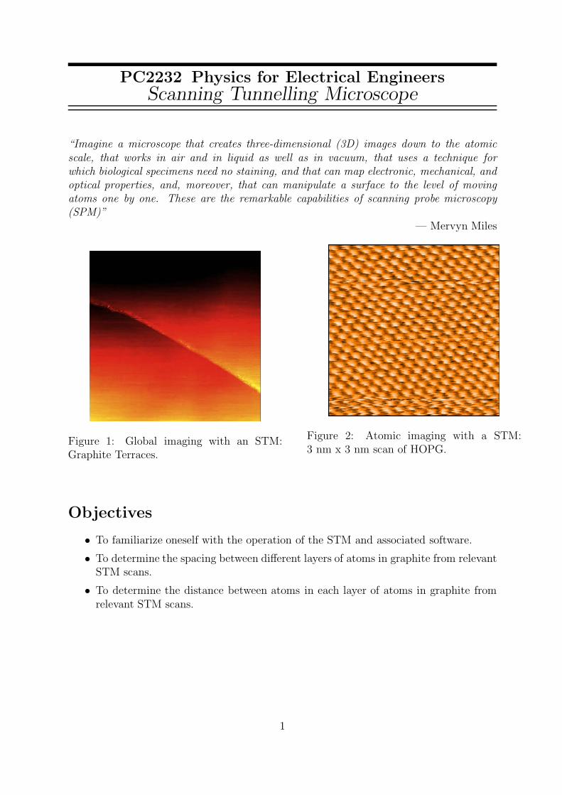
Figure 1: Global imaging with an STM:Graphite Terraces.
Figure 2: Atomic imaging with a STM:3 nm x 3 nm scan of HOPG.
Objectives
• To familiarize oneself with the operation of the STM and associated software.
• To determine the spacing between different layers of atoms in graphite from relevantSTM scans.
• To determine the distance between atoms in each layer of atoms in graphite fromrelevant STM scans.
1

Instruments & SetupFigure 3 shows the various components of the easyScan 2 setup. These are already
assembled and ready for your use.
(1) easyScan 2 controller, (2) easyScan 2 STM Scan Head, (3) Magnifying cover with10× magnifier, (4) USB cable (to connect controller to PC), (5) Mains cable, (6) STM
Tool set (see below) and (10) Vibration isolation platform
(1) Wire cutters, (2) Flat Nose Pliers, (3) Pointed tweezers (00D SA), (4) Roundedtweezers (2A SA-SL), (5) Sample holder, (6) Pt/Ir wire: 0.25mm/30cm for making
STM tips, (7) STM Basic Sample Kit with HOPG, gold thin film and four spare samplesupports.
Figure 3: The various components of the easyScan 2 setup..
Sample Preparation (if necessary)The HOPG (graphite) sample may be cleaved so as to obtain a clean surface as shown
in Figure 4 and described below:
2
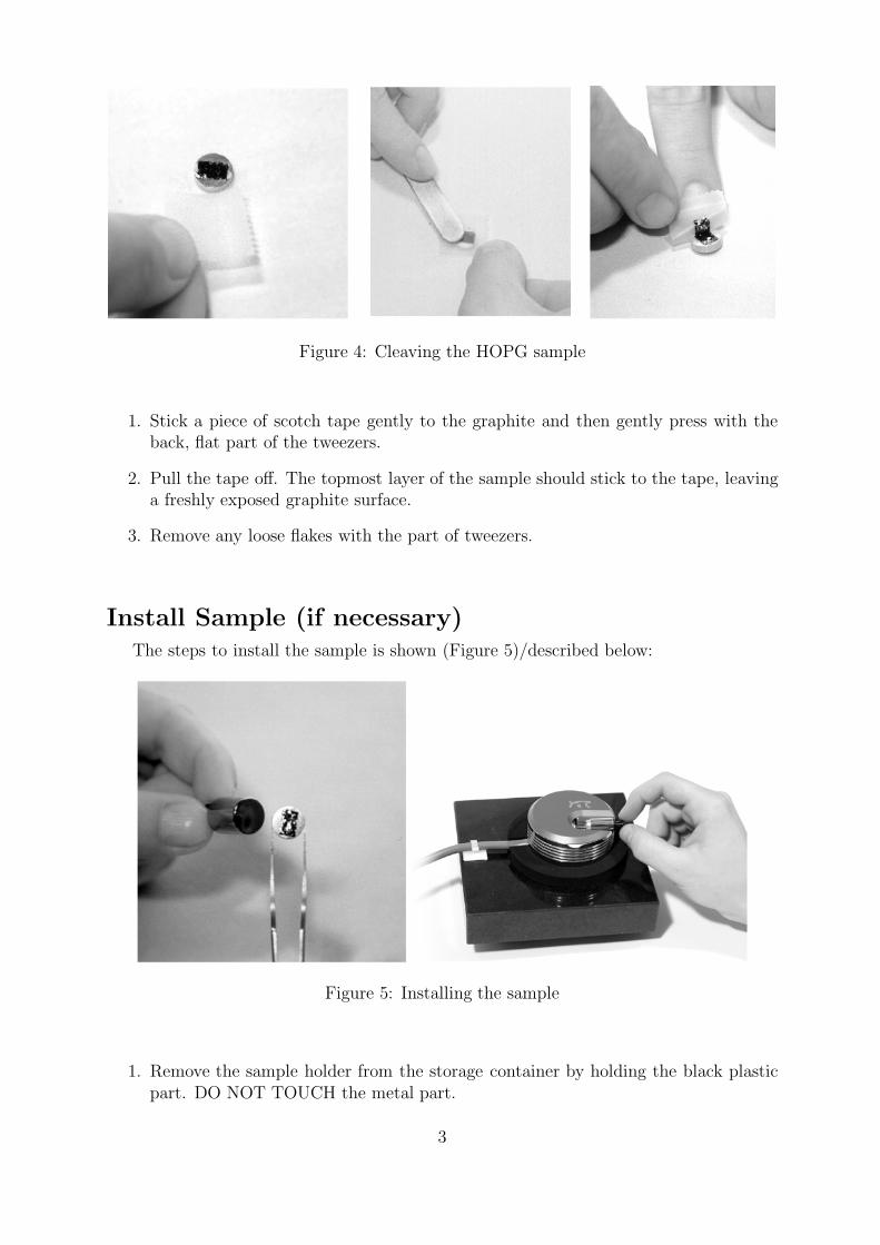
Figure 4: Cleaving the HOPG sample
1. Stick a piece of scotch tape gently to the graphite and then gently press with theback, flat part of the tweezers.
2. Pull the tape off. The topmost layer of the sample should stick to the tape, leavinga freshly exposed graphite surface.
3. Remove any loose flakes with the part of tweezers.
Install Sample (if necessary)The steps to install the sample is shown (Figure 5)/described below:
Figure 5: Installing the sample
1. Remove the sample holder from the storage container by holding the black plasticpart. DO NOT TOUCH the metal part.
3

2. Check for any contamination (dust, fingerprint) on the metal part. If cleaning isnecessary, follow the cleaning procedure.
(a) Moisten a cotton swab with ethanol and gently clean the surface.
(b) Allow the alcohol to completely dry.
3. First place it onto the little rails, then slide it onto the piezo motor. Make sure itdoes not touch the tip.
4. Using a tweezers, hold the graphite sample at the magnetic part.
5. Take the sample holder (handle at the black plastic part), and place the graphitesample on the magnet.
6. Push the sample holder very carefully to within a few mm of the tip.
Figure 6: Reflection of the tip off the graphite
Approach & Imaging
1. Important: The tip must not touch the sample or the tip may be damagedand would need to be replaced and the sample may need to be cleavedagain.
2. Through the magnifier, watch the distance between the tip and sample as you click‘Advance’ in the approach panel. The tip should be within a fraction of a millimetreto the surface. There should be a very small gap between the very end of the tipand the reflection of the end of the tip as can be seen in figure 6.
4

3. Set control parameters in Z-control panel (if necessary):
• Set point 1 nA
• P-gain 1000,
• I-gain 2000,
• Tip voltage 50 mV
4. Click ‘Approach’.
5. If the approach was completed successfully, the probe status light (see below)changed from blinking to green and automatically start to scan. This step mighttake some time depending of how close the the tip was positioned during coarseapproach. If the approach was unsuccessful, retract and try again.
6. Once the scanning has begun, you will need to optimise the tip-sample orientationas described next.
The Probe Status Light
The probe status light indicates the status of the Z-feedback loop that is responsiblefor controlling the tip-sample gap.
RED Scanner at it’s upper limit.Very strong tip-sample interaction.Possibility of a damaged tip.
ORANGE/YELLOW Scanner at it’s lower limit position.Weak tip-sample interactionTip possibly not in contact with the sample
GREEN Scanner not at either limit.Conditions good for imaging
BLINKING GREEN Feedback loop inactive.
Optimising the Image Plane (if necessary)
It is important that the plane of the lateral movement (i.e. the raster plane) of thetip be parallel to the sample (measurement, image) plane. Figure 7 shows this idea. Thefollowing are the steps to optimising the image plane.
1. Set the rotation to zero.
2. Observe the line scan. (An unoptimised plane will appear as shown in the figure onthe left 8).
3. Change ‘x-slope’ until the linescan becomes horizontal (figure on the right 8).
5

Figure 7: The important planes to keep in mind when using the easyScan 2
Figure 8: The effect of changing the x-slope. Before (left) and after (right).
4. Now change the rotation to 90◦ and optimise again, as above, but by changing the‘y-slope’.
Task 1 : Global Imaging - Looking for HOPG Terraces
It is not uncommon for the HOPG sample to be multi-layered so that scans over largeareas show ‘terraces’ as seen in figure 9.
Experiment
1. Obtain an image of a scan area of 500 nm x 500 nm using 256 x 256 pixels.
2. Suggested setting for Time / line is 0.3 s. (However, you may use other settings ifthat gives you better scans.)
6

Figure 9: HOPG terrace with lines draw using Gwyddion for the extraction of line profiles.
3. Locate a region with a terrace (see figure 9).
4. Reposition and zoom in (to around 100 nm x 100 nm) and obtain a good image.
5. Save as a .nid file.
6. Obtain one more good image (of about 100 nm x 100 nm) of another region of thisterrace and save the respective .nid files.
Analysis
1. Open the relevant .nid file in Gwyddion . (You may download the software fromhttp://gwyddion.net/)
2. Draw five (5) lines (similar to the one shown in figure 9 ) at right angles to theterrace step and obtain the profiles. You might want to increase the ‘thickness’ ofthe lines to obtain an averaged measurement.
3. Use ‘Edge Height’ function to extract the step heights for your lines profiles. Fig-ure 10 shows this feature in use.
7

Figure 10: Screenshots of extracting terrace information using Gwyddion
8

4. Save this image to include in your report.
5. Present the data for this measurements in the form of a table similar to the onebelow.
6. Repeat the above Experiment and Analysis for the other images of the terraceand produce a table of the form shown below.
measurement Terrace Regionregion 1 region 2
profile 1profile 2profile 3profile 4profile 5averagestd. dev.
7. Now add another row to the table that shows values foraverage
HOPG layer spacing.
8. Comment on the values of the heights of the terraces obtained with reference to thedata given for the HOPG in the theory section.
Task 2: Atomic Imaging
Experiment
1. Obtain an image at a scan area of 500 nm x 500 nm at 256 x 256 pixels.
2. Optimise and image for the scan sizes (bear in mind the pointers in the Hints Sectionbelow).
(a) 250 nm x 250 nm
(b) 50 nm x 50 nm
(c) 10 nm x 10 nm
(d) 4 nm x 4 nm (should be similar to figure 11)
3. Save a *.nid file for each of the above.
Measurement
1. Extract the surface roughness from the screen for each of the images obtained.Present this data in the form of a table as shown below.
9

Figure 11: 3 nm x 3 nm scan of HOPG using easyScan 2 . (Tip voltage: 50 mV, Setpoint: 1 nA, Time per line: 0.2 s)
Scan size (nm x nm) Roughness250 x 25050 x 5010 x 104 x 4
2. For the 250 nm x 250 nm and 50 nm x 50 nm scans, it is suggested that you continueto use 0.3 s scan per line. For 10 x 10 nm, reduce to 128 x 128 pixels at 0.03 s / lineuntil the system stabilises. Then increase back to 256 nm x 256 nm. Do the samefor 4 nm x 4 nm.
3. Apply appropriate filter, if necessary, to improve the contrast of your images.
4. Use your images to extract:
(a) lattice constant
(b) atom-to-atom distance
Make at least five measurements at different sites and present them in the form ofa table as shown below.
atom-to-atom distancemeasurement 1measurement 2measurement 3measurement 4measurement 5
averagestd. dev.
10

5. Describe the symmetry that your images of HOPG exhibit? Is this consistent withour understanding of the HOPG? Explain
Shutdown Procedures
1. Wear gloves.
2. Retract the STM tip as far as possible by auto-positioning.
3. Close the easyScan 2 software window.
4. Leave the STM tip on the head.
5. Take the sample off of the sample holder. Place the sample in its case.
6. Clean the sample holder with ethanol and a cotton swab. Let it dry.
7. Place the sample holder in the case. Close the cap tightly.
8. Place the STM cover over the STM head.
9. Turn off the controller power switch.
Hints & Tricks for better images
Optimize the “I-gain” and “P-gain” These values control error correction in thefeedback loop maintaining constant current. A useful strategy is to increase oneparameter slowly and watch for spikes to occur in the linescan, indicating that un-wanted oscillations are occurring in the feedback loop. Then back off one or twosteps until the linescan becomes smooth again.
Speed things up It is essential to apply short scanning times to minimise thermal drifteffects. So set time/line to as small as possible.
Give it a few scans The piezoelectric drivers can sometimes takes a finite time to settledown when it is started/restarted. So it is best to allow for a couple of scan beforeacquiring the final image.
Trouble with debris There can be instances where some debris might be attached tothe tip which will result in poor results. In such cases you may:
• Retract the tip and press the Cleaning Pulse button in the Tip Propertiessection of the ‘Z-Controller’ panel. (This momentarily increases the currentand ‘burns’ the debris off)
• Perform a new approach.
11

‘Rotate’ the tip The pull/tear method of producing a tip does not result in a rotation-ally symmetrical tip. This leads to a variation in the quality of images depending onhow the tip is oriented with respect to the raster pattern. This can be understoodby the schematic depicted in figure 12.
Overscan When imaging the tip is moved in a left-right raster pattern. This requires thetip to change its direction abruptly at the left and right edges. This sudden changecan cause instability in the smooth motion of the tip that can lead to deteriorationin the image quality. To avoid this the easyScan 2 offers the ‘overscan’ option thatallows space on the left and right sides of the scan for the tip to stabilize. Theseareas are not included in the final image (so your imaged area will appear smallerthan that indicated in scan area setting).
Change the value of the overscan to about 10%.
Figure 12: Schematic showing the effect of an asymmetrical tip. Notice that the conditionsof (a) will result in a more faithful reproduction of the rectangular ‘feature’ than those of(b).
Minimise Interference Bright light and movement near the STM setup can interferewith the measurement. Avoid abrupt movements and walking around in the room.
Finetune Image Plane When decreasing the scan range, look at the slope of the in-dividual line scans. Sometimes, they have to be re-adjusted (remember the 90◦
rotation).
12

Theory Supplement
Scanning Tunnelling Microscopy
Figure 13: The basic idea involved in scanning tunnelling microscopy. The tip is movedhorizontally in a raster pattern while moving the tip vertically so as to maintain a constanttunnelling current.
• The basic idea of scanning tunnelling microscopy, as depicted in figure 13, involvesscanning a sharp tip over a surface so as to maintain a given tunnelling current.This is achieved by moving the tip in the horizontal plane in a raster pattern whilesimultaneously adjusting the vertical tip distance. Owing to the exponential depen-dance of the tunnelling current on the sample-tip distance this is able to reproducefeatures of the surface with sub-nanometer resolution.
• In spite of the phenomenon of quantum mechanical tunnelling been known since the1920s, its use in microscopy was implemented only more recently in 1982, by Binniget al for which the 1986 Nobel Prize in Physics was awarded.
• The most significant feature of STM is the ability for real-space visualisation ofsurfaces at atomic scales.
• Since STM depends on a tunnelling current its applicability requires a conductingsample. A similar but more universal technique is atomic force microscopy (AFM)which does not have this restrictions.
• STM constant current images provide information about the variations in the elec-tron density and do not necessarily correspond to the location of atomic nuclei. Thisis further illustrated in figure 14.
13

Figure 14: Sketch of possible STM images relative to the nucleus locations. Top viewis the contour lines of constant intensity for the STM images that corresponds to theside view at the bottom. The STM image shows high tunnelling location at centre of twonuclei in (a) but at the top of each nucleus in (b).
• Varying STM parameters actually allows us to probe different aspects of certainstructures. For instance we may obtain two different images of the same sample bymerely changing the polarity of the tip. An example is shown in figure 15 whichuses the Si < 011 > surface.
Figure 15: STM images of a Si surface with (a) +1.8 V bias and (b) -1.8 V bias. Source:Lucia Vitali’s ([email protected]) PhD thesis.
14

Highly Ordered Pyroletic Graphite (HOPG)
Figure 16: Structure of Graphite (left) and Diamond (right), the two stable allotropes ofCarbon
• Carbon may be found in two allotropes: diamond and graphite.The relevant latticesfor these two allotropes is shown in figure 16.
• Diamond is an insulator and one of the hardest known materials.
• Graphite, in contrast to diamond, is a electrical conductor and softer and easilyflaked.
• Naturally found graphite exhibits an imperfect structure due to plenty of defectsand inclusions.
• Highly Ordered Pyroletic Graphite (HOPG) is a synthetic form of graphitethat exhibits a very high degree of three-dimensional ordering, especially in thealignment of adjacent layers.
• HOPG is an excellent tool for using in SPM as a substrate or calibration standard atatomic levels of resolution. This is an easily renewable material with an extremelysmooth surface. It has an ideal atomically flat surface and provides a backgroundwith only carbon in the elemental signature thus making results in a featurelessbackground. This is vital for SPM measurements that require uniform, flat, andclean substrates, for samples where elemental analysis is to be done.
• Graphite exhibits (figures 16 and 17) a layered structures with the atoms in agiven layer being covalently bonded in a hexagonal lattice. Adjacent layers are heldtogether by weak van der Waals bonds. This is why graphite can work as a goodlubricant.
• Graphite has its adjacent layers displaced relative to each other leading to the atomsof a layer either having a neighbour directly below (A atoms) or not (B atoms) ascan be observed in figure 17.
15
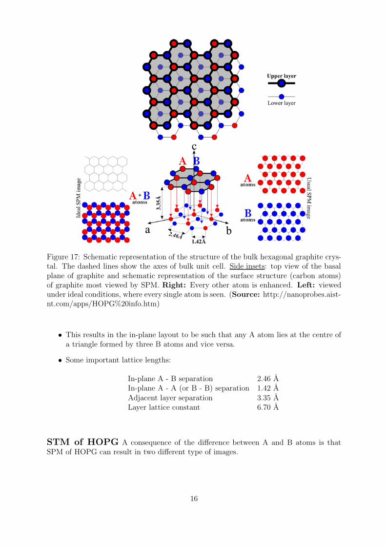
Figure 17: Schematic representation of the structure of the bulk hexagonal graphite crys-tal. The dashed lines show the axes of bulk unit cell. Side insets: top view of the basalplane of graphite and schematic representation of the surface structure (carbon atoms)of graphite most viewed by SPM. Right: Every other atom is enhanced. Left: viewedunder ideal conditions, where every single atom is seen. (Source: http://nanoprobes.aist-nt.com/apps/HOPG%20info.htm)
• This results in the in-plane layout to be such that any A atom lies at the centre ofa triangle formed by three B atoms and vice versa.
• Some important lattice lengths:
In-plane A - B separation 2.46 AIn-plane A - A (or B - B) separation 1.42 AAdjacent layer separation 3.35 ALayer lattice constant 6.70 A
STM of HOPG A consequence of the difference between A and B atoms is thatSPM of HOPG can result in two different type of images.
16

Figure 18: STM of HOPG. Left: Symmetric contrast. Right: “three-for-six”. Comparethese images with the schematic of figure 16
Symmetric contrast
• Under ideal conditions, SPM images of HOPG surface reveal a lattice of dark spotswith a lattice parameter of 2.46 A. (Figure 18)
• The six carbon atoms composed in hexagonal ring surrounding each spot give abright signal, which leads to a true honeycomb atomic pattern (symmetric contrast).
• The center to center atomic distance is 1.42 A.
“three-for-six”
• The atomic pattern normally observed in most SPM images under usual conditionsshows an asymmetric positive contrast in that bright spots originate from only three(the B atoms) of the set of six atoms that form a graphene hexagon unit cell of thegraphite lattice.
• Each apparent atom is surrounded by six nearest neighbors. These form the verticesof the yellow hexagon of figure 18 . The distance between any two of these atomsis 2.46 A.
• This asymmetry in the surface atom environment results in a threefold symmetry(“three-for-six”) pattern as observed in the picture on the right of figure 18.
17