Embed Size (px)
Citation preview

Part Number 440EP
Revision 1.29 – May 07, 2008
AMCC Proprietary 1
440EPPowerPC 440EP Embedded Processor
Data Sheet
Features
• PowerPC® 440 processor core operating up to 667MHz with 32KB I-cache and D-cache with parity checking.
• Selectable processor:bus clock ratios of N:1, N:2.
• Floating Point Unit with single- and double-precision and single-cycle throughput.
• Dual bridged Processor Local Buses (PLBs) with 64- and 128-bit widths.
• Double Data Rate (DDR) Synchronous DRAM (SDRAM) interface operating up to 133MHz with ECC.
• DMA support for external peripherals, internal UART and memory.
• PCI V2.2 interface (3.3V only). Thirty-two bits at up to 66MHz.
• Programmable interrupt controller supports interrupts from a variety of sources.
• Programmable General Purpose Timers (GPT).
• Two Ethernet 10/100Mbps half- or full-duplex interfaces. Operational modes supported are MII, RMII, and SMII with packet reject.
• Up to four serial ports (16550 compatible UART).
• Two USB ports. One USB 1.1 Host interface with on-chip PHY. One USB 2.0 Device interface, with dedicated DMA, configured as a 1.1 on-chip PHY or a 2.0 UTMI.
• External peripheral bus (16-bit data) for up to six devices with external mastering.
• Two IIC interfaces (one with boot parameter read capability).
• NAND Flash interface.
• SPI interface.
• General Purpose I/O (GPIO) interface.
• JTAG interface for board level testing.
• Boot from PCI memory, NOR Flash on the external peripheral bus, or NAND Flash on the NAND Flash interface.
• Available in RoHS compliant lead-free package.
Description
Designed specifically to address high-end embedded applications, the PowerPC 440EP (PPC440EP) provides a high-performance, low- power solution that interfaces to a wide range of peripherals and incorporates on-chip power management features.
This chip contains a high-performance RISC processor, a floating point unit, DDR SDRAM controller, PCI bus interface, control for external ROM and peripherals, DMA with scatter-gather support, Ethernet ports, serial ports, IIC interfaces, SPI interface, USB ports, NAND Flash interface, and general purpose I/O.
Technology: CMOS Cu-11, 0.13μm.
Package: 35mm, 456-ball standard plastic ball grid array (E-PBGA), with and without lead (RoHS compliant).
Typical power (measured): Less than 3W at 533MHz, 2.5W at 400MHz.
Supply voltages required: 3.3V, 2.5V, 1.5V.

2 AMCC Proprietary
440EP – PPC440EP Embedded ProcessorRevision 1.29 – May 07, 2008Data Sheet
ContentsOrdering and PVR Information . . . . . . . . . . . . . . . . . . . . . . . . . . . . . . . . . . . . . . . . . . . . . . . . . . . . . . . . . . . . . . . 5Address Maps . . . . . . . . . . . . . . . . . . . . . . . . . . . . . . . . . . . . . . . . . . . . . . . . . . . . . . . . . . . . . . . . . . . . . . . . . . . . 7Block Diagram . . . . . . . . . . . . . . . . . . . . . . . . . . . . . . . . . . . . . . . . . . . . . . . . . . . . . . . . . . . . . . . . . . . . . . . . . . . . 6PowerPC 440 Processor Core . . . . . . . . . . . . . . . . . . . . . . . . . . . . . . . . . . . . . . . . . . . . . . . . . . . . . . . . . . . . . . 10Internal Buses . . . . . . . . . . . . . . . . . . . . . . . . . . . . . . . . . . . . . . . . . . . . . . . . . . . . . . . . . . . . . . . . . . . . . . . . . . . 11Floating Point Unit (FPU) . . . . . . . . . . . . . . . . . . . . . . . . . . . . . . . . . . . . . . . . . . . . . . . . . . . . . . . . . . . . . . . . . . 10PCI Interface . . . . . . . . . . . . . . . . . . . . . . . . . . . . . . . . . . . . . . . . . . . . . . . . . . . . . . . . . . . . . . . . . . . . . . . . . . . . 12DDR SDRAM Memory Controller . . . . . . . . . . . . . . . . . . . . . . . . . . . . . . . . . . . . . . . . . . . . . . . . . . . . . . . . . . . . 12External Peripheral Bus Controller (EBC) . . . . . . . . . . . . . . . . . . . . . . . . . . . . . . . . . . . . . . . . . . . . . . . . . . . . . . 13Ethernet Controller Interface . . . . . . . . . . . . . . . . . . . . . . . . . . . . . . . . . . . . . . . . . . . . . . . . . . . . . . . . . . . . . . . . 13DMA to PLB3 Controller . . . . . . . . . . . . . . . . . . . . . . . . . . . . . . . . . . . . . . . . . . . . . . . . . . . . . . . . . . . . . . . . . . . 13DMA to PLB4 Controller . . . . . . . . . . . . . . . . . . . . . . . . . . . . . . . . . . . . . . . . . . . . . . . . . . . . . . . . . . . . . . . . . . . 14Serial Ports (UART) . . . . . . . . . . . . . . . . . . . . . . . . . . . . . . . . . . . . . . . . . . . . . . . . . . . . . . . . . . . . . . . . . . . . . . 14IIC Bus Interface . . . . . . . . . . . . . . . . . . . . . . . . . . . . . . . . . . . . . . . . . . . . . . . . . . . . . . . . . . . . . . . . . . . . . . . . . 14Serial Peripheral Interface (SPI/SCP) . . . . . . . . . . . . . . . . . . . . . . . . . . . . . . . . . . . . . . . . . . . . . . . . . . . . . . . . . 15Universal Serial Bus (USB) . . . . . . . . . . . . . . . . . . . . . . . . . . . . . . . . . . . . . . . . . . . . . . . . . . . . . . . . . . . . . . . . . 15NAND Flash Controller . . . . . . . . . . . . . . . . . . . . . . . . . . . . . . . . . . . . . . . . . . . . . . . . . . . . . . . . . . . . . . . . . . . . 15General Purpose Timers (GPT) . . . . . . . . . . . . . . . . . . . . . . . . . . . . . . . . . . . . . . . . . . . . . . . . . . . . . . . . . . . . . 16General Purpose IO (GPIO) Controller . . . . . . . . . . . . . . . . . . . . . . . . . . . . . . . . . . . . . . . . . . . . . . . . . . . . . . . . 16Universal Interrupt Controller (UIC) . . . . . . . . . . . . . . . . . . . . . . . . . . . . . . . . . . . . . . . . . . . . . . . . . . . . . . . . . . . 16JTAG . . . . . . . . . . . . . . . . . . . . . . . . . . . . . . . . . . . . . . . . . . . . . . . . . . . . . . . . . . . . . . . . . . . . . . . . . . . . . . . . . . 16Package Diagram . . . . . . . . . . . . . . . . . . . . . . . . . . . . . . . . . . . . . . . . . . . . . . . . . . . . . . . . . . . . . . . . . . . . . . . . 17Signal Lists . . . . . . . . . . . . . . . . . . . . . . . . . . . . . . . . . . . . . . . . . . . . . . . . . . . . . . . . . . . . . . . . . . . . . . . . . . . . . 19Signal Descriptions . . . . . . . . . . . . . . . . . . . . . . . . . . . . . . . . . . . . . . . . . . . . . . . . . . . . . . . . . . . . . . . . . . . . . . . 50Device Characteristics . . . . . . . . . . . . . . . . . . . . . . . . . . . . . . . . . . . . . . . . . . . . . . . . . . . . . . . . . . . . . . . . . . . . 61Spread Spectrum Clocking . . . . . . . . . . . . . . . . . . . . . . . . . . . . . . . . . . . . . . . . . . . . . . . . . . . . . . . . . . . . . . . . . 68I/O Specifications . . . . . . . . . . . . . . . . . . . . . . . . . . . . . . . . . . . . . . . . . . . . . . . . . . . . . . . . . . . . . . . . . . . . . . . . 69DDR1 SDRAM I/O Specifications . . . . . . . . . . . . . . . . . . . . . . . . . . . . . . . . . . . . . . . . . . . . . . . . . . . . . . . . . . . . 75DDR SDRAM Write Operation . . . . . . . . . . . . . . . . . . . . . . . . . . . . . . . . . . . . . . . . . . . . . . . . . . . . . . . . . . . . . . 77DDR SDRAM Read Operation . . . . . . . . . . . . . . . . . . . . . . . . . . . . . . . . . . . . . . . . . . . . . . . . . . . . . . . . . . . . . . 79Strapping . . . . . . . . . . . . . . . . . . . . . . . . . . . . . . . . . . . . . . . . . . . . . . . . . . . . . . . . . . . . . . . . . . . . . . . . . . . . . . . 84EEPROM . . . . . . . . . . . . . . . . . . . . . . . . . . . . . . . . . . . . . . . . . . . . . . . . . . . . . . . . . . . . . . . . . . . . . . . . . . . . . . 84

AMCC Proprietary 3
440EP – PPC440EP Embedded ProcessorData Sheet
Revision 1.29 – May 07, 2008
FiguresFigure 1. Order Part Number Key . . . . . . . . . . . . . . . . . . . . . . . . . . . . . . . . . . . . . . . . . . . . . . . . . . . . . . . . . . . . . 5Figure 2. PPC440EP Functional Block Diagram . . . . . . . . . . . . . . . . . . . . . . . . . . . . . . . . . . . . . . . . . . . . . . . . . . 6Figure 3. 35mm, 456-Ball E-PBGA . . . . . . . . . . . . . . . . . . . . . . . . . . . . . . . . . . . . . . . . . . . . . . . . . . . . . . . . . . . 17Figure 4. Overshoot Waveform . . . . . . . . . . . . . . . . . . . . . . . . . . . . . . . . . . . . . . . . . . . . . . . . . . . . . . . . . . . . . . 63Figure 5. Timing Waveform . . . . . . . . . . . . . . . . . . . . . . . . . . . . . . . . . . . . . . . . . . . . . . . . . . . . . . . . . . . . . . . . . 67Figure 6. Input Setup and Hold Waveform . . . . . . . . . . . . . . . . . . . . . . . . . . . . . . . . . . . . . . . . . . . . . . . . . . . . . 70Figure 7. Output Delay and Float Timing Waveform . . . . . . . . . . . . . . . . . . . . . . . . . . . . . . . . . . . . . . . . . . . . . . 70Figure 8. DDR SDRAM Simulation Signal Termination Model . . . . . . . . . . . . . . . . . . . . . . . . . . . . . . . . . . . . . . 75Figure 9. DDR SDRAM Write Cycle Timing . . . . . . . . . . . . . . . . . . . . . . . . . . . . . . . . . . . . . . . . . . . . . . . . . . . . 77Figure 10. DDR SDRAM MemClkOut0 and Read Clock Delay . . . . . . . . . . . . . . . . . . . . . . . . . . . . . . . . . . . . . 79Figure 11. DDR SDRAM Read Data Path . . . . . . . . . . . . . . . . . . . . . . . . . . . . . . . . . . . . . . . . . . . . . . . . . . . . . 80Figure 12. DDR SDRAM Read Cycle Timing—Example 1 . . . . . . . . . . . . . . . . . . . . . . . . . . . . . . . . . . . . . . . . . 81Figure 13. DDR SDRAM Read Cycle Timing—Example 2 . . . . . . . . . . . . . . . . . . . . . . . . . . . . . . . . . . . . . . . . . 82Figure 14. DDR SDRAM Read Cycle Timing—Example 3 . . . . . . . . . . . . . . . . . . . . . . . . . . . . . . . . . . . . . . . . . 83
TablesTable 1. System Memory Address Map . . . . . . . . . . . . . . . . . . . . . . . . . . . . . . . . . . . . . . . . . . . . . . . . . . . . . . . . 7Table 2. DCR Address Map (4KB of Device Configuration Registers) . . . . . . . . . . . . . . . . . . . . . . . . . . . . . . . . . 9Table 3. Recommended Reflow Soldering Profile . . . . . . . . . . . . . . . . . . . . . . . . . . . . . . . . . . . . . . . . . . . . . . . 18Table 4. JEDEC Moisture Sensitivity Level and Ball Composition . . . . . . . . . . . . . . . . . . . . . . . . . . . . . . . . . . . 18Table 5. Signals Listed Alphabetically . . . . . . . . . . . . . . . . . . . . . . . . . . . . . . . . . . . . . . . . . . . . . . . . . . . . . . . . 19Table 6. Signals Listed by Ball Assignment . . . . . . . . . . . . . . . . . . . . . . . . . . . . . . . . . . . . . . . . . . . . . . . . . . . . 43Table 7. Pin Summary . . . . . . . . . . . . . . . . . . . . . . . . . . . . . . . . . . . . . . . . . . . . . . . . . . . . . . . . . . . . . . . . . . . . 50Table 8. Signal Functional Description . . . . . . . . . . . . . . . . . . . . . . . . . . . . . . . . . . . . . . . . . . . . . . . . . . . . . . . . 52Table 9. Absolute Maximum Ratings . . . . . . . . . . . . . . . . . . . . . . . . . . . . . . . . . . . . . . . . . . . . . . . . . . . . . . . . . 61Table 10. Recommended DC Operating Conditions . . . . . . . . . . . . . . . . . . . . . . . . . . . . . . . . . . . . . . . . . . . . . . 61Table 11. Overshoot and Undershoot . . . . . . . . . . . . . . . . . . . . . . . . . . . . . . . . . . . . . . . . . . . . . . . . . . . . . . . . . 63Table 12. Input Capacitance . . . . . . . . . . . . . . . . . . . . . . . . . . . . . . . . . . . . . . . . . . . . . . . . . . . . . . . . . . . . . . . . 64Table 13. Typical DC Power Supply Requirements . . . . . . . . . . . . . . . . . . . . . . . . . . . . . . . . . . . . . . . . . . . . . . 64Table 14. VDD Supply Power Dissipation . . . . . . . . . . . . . . . . . . . . . . . . . . . . . . . . . . . . . . . . . . . . . . . . . . . . . . 65
Table 15. DC Power Supply Current Loads . . . . . . . . . . . . . . . . . . . . . . . . . . . . . . . . . . . . . . . . . . . . . . . . . . . . 65Table 16. Package Thermal Specifications . . . . . . . . . . . . . . . . . . . . . . . . . . . . . . . . . . . . . . . . . . . . . . . . . . . . . 66Table 17. Clocking Specifications . . . . . . . . . . . . . . . . . . . . . . . . . . . . . . . . . . . . . . . . . . . . . . . . . . . . . . . . . . . . 67Table 18. Peripheral Interface Clock Timings . . . . . . . . . . . . . . . . . . . . . . . . . . . . . . . . . . . . . . . . . . . . . . . . . . . 69Table 19. I/O Specifications—PCI, USB, UART, IIC, SPI, Ethernet, System and Debug Interfaces . . . . . . . . . 71Table 20. I/O Specifications—EBC, EBMI, DMA and NAND Flash Interfaces . . . . . . . . . . . . . . . . . . . . . . . . . . 74Table 21. DDR SDRAM Output Driver Specifications . . . . . . . . . . . . . . . . . . . . . . . . . . . . . . . . . . . . . . . . . . . . . 76Table 22. I/O Timing—DDR SDRAM TDS . . . . . . . . . . . . . . . . . . . . . . . . . . . . . . . . . . . . . . . . . . . . . . . . . . . . . . 78
Table 23. I/O Timing—DDR SDRAM TSK, TSA, and THA . . . . . . . . . . . . . . . . . . . . . . . . . . . . . . . . . . . . . . . . . . 78
Table 24. I/O Timing—DDR SDRAM TSD and THD . . . . . . . . . . . . . . . . . . . . . . . . . . . . . . . . . . . . . . . . . . . . . . . 78

4 AMCC Proprietary
440EP – PPC440EP Embedded ProcessorRevision 1.29 – May 07, 2008Data Sheet
Table 25. I/O Timing—DDR SDRAM TSIN and TDIN . . . . . . . . . . . . . . . . . . . . . . . . . . . . . . . . . . . . . . . . . . . . . . 80
Table 26. Strapping Pin Assignments . . . . . . . . . . . . . . . . . . . . . . . . . . . . . . . . . . . . . . . . . . . . . . . . . . . . . . . . . 84

AMCC Proprietary 5
440EP – PPC440EP Embedded ProcessorData Sheet
Revision 1.29 – May 07, 2008
Ordering and PVR Information
For information on the availability of the following parts, contact your local AMCC sales office.
Each part number contains a revision code. This is the die mask revision number and is included in the part number for identification purposes only.
The PVR (Processor Version Register) and the JTAG ID register are software accessible (read-only) and contain information that uniquely identifies the part. Refer to the PPC440EP User’s Manual for details on accessing these registers.
Figure 1. Order Part Number Key
Product Name Order Part Number(see Notes:) Package Revision
Level PVR Value JTAG ID
PPC440EP PPC440EP-3pbfffCx 35mm, 456 ball, E-PBGA C 0x422218D4 0x2A950049
Notes:1. p = Module Package type
B = standard (E-PBGA) and contains lead.J = standard (E-PBGA) and is lead-free (RoHS compliant)
2. b = Chip revision levelC = Revision level C (2.1)
3. fff = Processor frequency333 = 333MHz400 = 400MHz533 = 533MHz667 = 667MHz
4. C = Case temperature range:-40°C to + 90°C for 333MHz and 400 MHz parts-40°C to +100°C for 533MHz parts-40°C to +85°C for 667MHz parts
5. x = Shipping package typeZ = tape-and-reelBlank = tray
AMCC Part Number
PPC440EP-3JC667CZ
Package
Processor FrequencyGrade 3 Reliability
Case Temperature Range
Revision Level
Shipping Package
Note: The example P/N above is a standard lead-free, revision C package, capable of running at667MHz, and is shipped in tape-and-reel packaging.

6 AMCC Proprietary
440EP – PPC440EP Embedded ProcessorRevision 1.29 – May 07, 2008Data Sheet
Block Diagram
Figure 2. PPC440EP Functional Block Diagram
The PPC440EP is a system on a chip (SOC) using IBM CoreConnect Bus™ Architecture.
Processor Core DCR Bus
32KB
On-chip Peripheral Bus (OPB 0)
GPIO IIC UART
PLB (PLB4—128 bits)
DDR SDRAM
ExternalPeripheralController
Controller
ClockControlReset
PowerMgmt
JTAG Trace
Timers
MMU- 30-bit addr- 16-bit data
- 13-bit addr- 32-bit data
NANDFlash
Controller
UIC
I-Cache32KB
D-Cache
PPC440
PCIBridge
x2 x4 MALEthernet
x2
DCRs
GPT
1 MIIor2 RMIIor2 SMII
ZMII
66MHz max
10/100
66MHz max
266MHz data rate
PLB (PLB3—64 bits)PLB
Bridge
SPIUSB 2.0
- 32 bits- 6 devices
PerformanceMonitor
FPU
External
DMAController
OPBBridge
BSC
10
UTMI
DMAController
OPBBridge
1.1PHY
D+/D−
OPB 1
USB 1.1Host
1.1PHY
Device
D+/D−
Interrupts

AMCC Proprietary 7
440EP – PPC440EP Embedded ProcessorData Sheet
Revision 1.29 – May 07, 2008
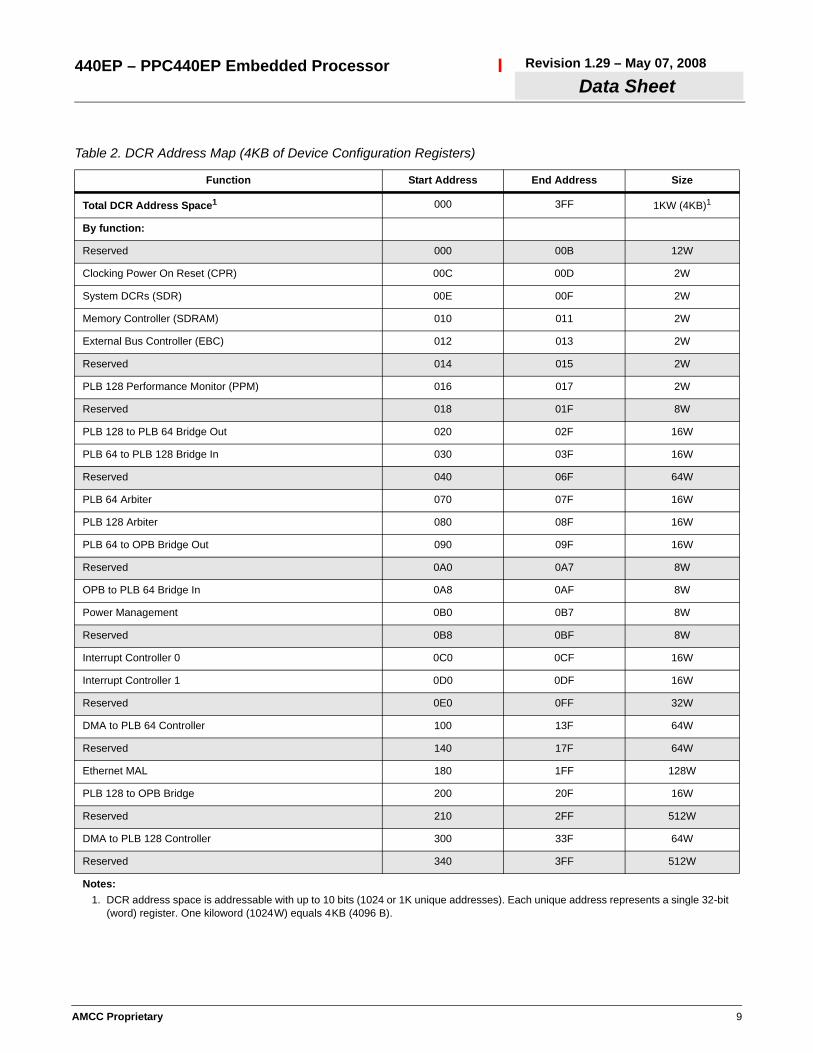
Address Maps
The PPC440EP incorporates two address maps. The first is a fixed processor System Memory Address Map. This address map defines the possible contents of various address regions which the processor can access. The second is the DCR Address Map for Device Configuration Registers (DCRs). The DCRs are accessed by software running on the PPC440EP processor through the use of mtdcr and mfdcr instructions.
Table 1. System Memory Address Map (Sheet 1 of 2)
Function Sub Function Start Address End Address Size
Local Memory1DDR SDRAM 0 0000 0000 0 3FFF FFFF 1GB
Reserved 0 4000 0000 0 4FFF FFFF
USB 2.0 Device Bus
OPB Arbiter for USB (OPB 1) 0 5000 0000 0 5000 003F 64B
Reserved 0 5000 0040 0 5000 00FF
USB 2.0 Device 0 5000 0100 0 5000 017F 128B
Reserved 0 5000 0180 0 7FFF FFFF
EBC EBC 0 8000 0000 0 9FFF FFFF 512MB
PCI
PCI Memory 0 A000 0000 0 DFFF FFFF 1GB
Reserved 0 E000 0000 0 E7FF FFFF
PCI I/O 0 E800 0000 0 E800 FFFF 64KB
Reserved 0 E801 0000 0 E87F FFFF
PCI I/O 0 E880 0000 0 EBFF FFFF 56MB
Reserved 0 EC00 0000 0 EEBF FFFF
Configuration Registers 0 EEC0 0000 0 EEC0 0007 8B
Reserved 0 EEC0 0008 0 EECF FFFF
PCI Interrupt Ack / Special Cycle 0 EED0 0000 0 EED0 0003 4B
Reserved 0 EED0 0004 0 EF3F FFFF
Local Configuration Registers 0 EF40 0000 0 EF40 003F 64B
Reserved 0 EF40 0040 0 EF4F FFFF

8 AMCC Proprietary
440EP – PPC440EP Embedded ProcessorRevision 1.29 – May 07, 2008Data Sheet
Internal Peripherals
Reserved 0 EF50 0000 0 EF5F FFFF
General Purpose Timer 0 EF60 0000 0 EF60 00FF 256B
Reserved 0 EF60 0100 0 EF60 02FF
UART0 0 EF60 0300 0 EF60 0307 8B
Reserved 0 EF60 0308 0 EF60 03FF
UART1 0 EF60 0400 0 EF60 0407 8B
Reserved 0 EF60 0408 0 EF60 04FF
UART2 0 EF60 0500 0 EF60 0507 8B
Reserved 0 EF60 0508 0 EF60 05FF
UART3 0 EF60 0600 0 EF60 0607 8B
Reserved 0 EF60 0608 0 EF60 06FF
IIC0 0 EF60 0700 0 EF60 071F 32B
Reserved 0 EF60 0720 0 EF60 07FF
IIC1 0 EF60 0800 0 EF60 081F 32B
Reserved 0 EF60 0820 0 EF60 08FF
SPI 0 EF60 0900 0 EF60 0906 6B
Reserved 0 EF60 0907 0 EF60 09FF
OPB Arbiter (OPB 0) 0 EF60 0A00 0 EF60 0A3F 64B
Reserved 0 EF60 0A40 0 EF60 0AFF
GPIO0 Controller 0 EF60 0B00 0 EF60 0B7F 128B
Reserved 0 EF60 0B80 0 EF60 0BFF
GPIO1 Controller 0 EF60 0C00 0 EF60 0C7F 128B
Reserved 0 EF60 0C80 0 EF60 0CFF
Ethernet PHY ZMII 0 EF60 0D00 0 EF60 0D0F 16B
Reserved 0 EF60 0D10 0 EF60 0DFF
Ethernet 0 Controller 0 EF60 0E00 0 EF60 0EFF 256B
Ethernet 1 Controller 0 EF60 0F00 0 EF60 0FFF 256B
USB 1.1 Host 0 EF60 1000 0 EF60 107F 128B
Reserved 0 EF60 1080 0 EFFF FFFF
EBC 0 F000 0000 0 FFDF FFFF 254MB
Boot space (EBC Bank 0 and PCI) 0 FFE0 0000 0 FFFF FFFF 2MB
Notes:1. DDR SDRAM can be located anywhere in the Local Memory area of the memory map.2. EBC and PCI are relocatable, but this map reflects the suggested configuration.
Table 1. System Memory Address Map (Sheet 2 of 2)
Function Sub Function Start Address End Address Size
AMCC Proprietary 9
440EP – PPC440EP Embedded ProcessorData Sheet
Revision 1.29 – May 07, 2008
Table 2. DCR Address Map (4KB of Device Configuration Registers)
Function Start Address End Address Size
Total DCR Address Space1 000 3FF 1KW (4KB)1
By function:
Reserved 000 00B 12W
Clocking Power On Reset (CPR) 00C 00D 2W
System DCRs (SDR) 00E 00F 2W
Memory Controller (SDRAM) 010 011 2W
External Bus Controller (EBC) 012 013 2W
Reserved 014 015 2W
PLB 128 Performance Monitor (PPM) 016 017 2W
Reserved 018 01F 8W
PLB 128 to PLB 64 Bridge Out 020 02F 16W
PLB 64 to PLB 128 Bridge In 030 03F 16W
Reserved 040 06F 64W
PLB 64 Arbiter 070 07F 16W
PLB 128 Arbiter 080 08F 16W
PLB 64 to OPB Bridge Out 090 09F 16W
Reserved 0A0 0A7 8W
OPB to PLB 64 Bridge In 0A8 0AF 8W
Power Management 0B0 0B7 8W
Reserved 0B8 0BF 8W
Interrupt Controller 0 0C0 0CF 16W
Interrupt Controller 1 0D0 0DF 16W
Reserved 0E0 0FF 32W
DMA to PLB 64 Controller 100 13F 64W
Reserved 140 17F 64W
Ethernet MAL 180 1FF 128W
PLB 128 to OPB Bridge 200 20F 16W
Reserved 210 2FF 512W
DMA to PLB 128 Controller 300 33F 64W
Reserved 340 3FF 512W
Notes:1. DCR address space is addressable with up to 10 bits (1024 or 1K unique addresses). Each unique address represents a single 32-bit
(word) register. One kiloword (1024W) equals 4KB (4096 B).

10 AMCC Proprietary
440EP – PPC440EP Embedded ProcessorRevision 1.29 – May 07, 2008Data Sheet
PowerPC 440 Processor Core
The PowerPC 440 processor core is designed for high-end applications: RAID controllers, SAN, iSCSI, routers, switches, printers, set-top boxes, etc. It is the first processor core to implement the new Book E PowerPC embedded architecture and the first to use the 128-bit version of IBM’s on-chip CoreConnect Bus Architecture.
Features include:• Up to 667MHz operation• PowerPC Book E architecture• 32KB I-cache, 32KB D-cache
– UTLB Word Wide parity on data and tag address parity with exception force• Three logical regions in D-cache: locked, transient, normal• D-cache full line flush capability• 41-bit virtual address, 36-bit (64GB) physical address• Superscalar, out-of-order execution• 7-stage pipeline• 3 execution pipelines• Dynamic branch prediction• Memory management unit
– 64-entry, full associative, unified TLB with optional parity– Separate instruction and data micro-TLBs– Storage attributes for write-through, cache-inhibited, guarded, and big or little endian
• Debug facilities– Multiple instruction and data range breakpoints– Data value compare– Single step, branch, and trap events– Non-invasive real-time trace interface
• 24 DSP instructions– Single cycle multiply and multiply-accumulate– 32 x 32 integer multiply– 16 x 16 -> 32-bit MAC
Floating Point Unit (FPU)
Features include:• Five stages with 2 MFlops/MHz• Hardware support for IEEE 754• Single- and double-precision• Single-cycle throughput on most instructions• Thirty-two 64-bit floating point registers

AMCC Proprietary 11
440EP – PPC440EP Embedded ProcessorData Sheet
Revision 1.29 – May 07, 2008
Internal Buses
The PowerPC 440EP features five standard on-chip buses: two Processor Local Buses (PLBs), two On-Chip Peripheral Buses (OPBs), and the Device Control Register Bus (DCR). The high performance, high bandwidth cores such as the PowerPC 440 processor core, the DDR SDRAM memory controller, and the PCI bridge connect to the PLBs. The primary OPB hosts lower data rate peripherals. The secondary OPB is dedicated to USB 2.0 and DMA. The daisy-chained DCR provides a lower bandwidth path for passing status and control information between the processor core and the other on-chip cores.
Features include:• PLB4
– 128-bit implementation of the PLB architecture– Separate and simultaneous read and write data paths– 36-bit address– Simultaneous control, address, and data phases– Four levels of pipelining– Byte-enable capability supporting unaligned transfers– 32- and 64-byte burst transfers– 133MHz, maximum 4.25GB/s (simultaneous read and write)– Processor:bus clock ratios of N:1 and N:2
• PLB3– 64-bit implementation of the PLB architecture– 32-bit address– 133MHz (1:1 ratio with PLB 128), maximum 1.1GB/s (no simultaneous read and write)
• OPB (2)– 32-bit data path– 32-bit address– 66.66MHz
• DCR– 32-bit data path– 10-bit address

12 AMCC Proprietary
440EP – PPC440EP Embedded ProcessorRevision 1.29 – May 07, 2008Data Sheet
PCI InterfaceThe PCI interface allows connection of PCI devices to the PowerPC processor and local memory. This interface is designed to Version 2.2 of the PCI Specification and supports 32- bit PCI devices.
Reference Specifications:• PowerPC CoreConnect Bus (PLB) Specification Version 3.1• PCI Specification Version 2.2• PCI Bus Power Management Interface Specification Version 1.1
Features include:• PCI 2.2
– Frequency to 66MHz– 32-bit bus
• PCI Host Bus Bridge or an Adapter Device's PCI interface• Internal PCI arbitration function, supporting up to six external devices, that can be disabled for use with an
external arbiter• Support for Message Signaled Interrupts• Simple message passing capability• Asynchronous to the PLB• PCI Power Management 1.1• PCI register set addressable both from on-chip processor and PCI device sides• Ability to boot from PCI bus memory• Error tracking/status• Supports initiation of transfer to the following address spaces:
– Single beat I/O reads and writes– Single beat and burst memory reads and writes– Single beat configuration reads and writes (type 0 and type 1)– Single beat special cycles
DDR SDRAM Memory Controller
The Double Data Rate (DDR) SDRAM memory controller supports industry standard discrete devices. Up to four 256MB logical banks are supported in limited configurations. Global memory timings, address and bank sizes, and memory addressing modes are programmable.
Features include:• Registered and non-registered industry standard discrete devices• 32-bit memory interface with optional 8-bit ECC (SEC/DED)• Sustainable 1.1GB/s peak bandwidth at 133MHz• SSTL_2 logic• 1 to 4 chip selects• CAS latencies of 2, 2.5 and 3 supported• DDR200/266 support• Page mode accesses (up to eight open pages) with configurable paging policy• Programmable address mapping and timing• Hardware and software initiated self-refresh• Power management (self-refresh, suspend, sleep)

AMCC Proprietary 13
440EP – PPC440EP Embedded ProcessorData Sheet
Revision 1.29 – May 07, 2008
External Peripheral Bus Controller (EBC)
Features include:• Up to six ROM, EPROM, SRAM, Flash memory, and slave peripheral I/O banks supported• Up to 66.66MHz operation• Burst and non-burst devices• 16-bit byte-addressable data bus• 30-bit address• Peripheral Device pacing with external “Ready”• Latch data on Ready, synchronous or asynchronous• Programmable access timing per device
– 256 Wait States for non-burst– 32 Burst Wait States for first access and up to 8 Wait States for subsequent accesses– Programmable CSon, CSoff relative to address – Programmable OEon, WEon, WEoff (1 to 4 clock cycles) relative to CS
• Programmable address mapping• External DMA Slave Support• External master interface
– Write posting from external master– Read prefetching on PLB for external master reads– Bursting capable from external master– Allows external master access to all non-EBC PLB slaves– External master can control EBC slaves for own access and control
Ethernet Controller Interface
Ethernet support provided by the PPC440EP interfaces to the physical layer but the PHY is not included on the chip:
• One to two 10/100 interfaces running in full- and half-duplex modes– One full Media Independent Interface (MII) with 4-bit parallel data transfer– Two Reduced Media Independent Interfaces (RMII) with 2-bit parallel data transfer– Two Serial Media Independent Interfaces (SMII)– Packet reject support
DMA to PLB3 Controller
This DMA controller provides a DMA interface between the OPB and the 64-bit PLB.
Features include:• Supports the following transfers:
– Memory-to-memory transfers– Buffered peripheral to memory transfers– Buffered memory to peripheral transfers
• Four channels• Scatter/Gather capability for programming multiple DMA operations• 32-byte buffer• 8-, 16-, 32-bit peripheral support (OPB and external)• 32-bit addressing• Address increment or decrement• Supports internal and external peripherals• Support for memory mapped peripherals• Support for peripherals running on slower frequency buses
14 AMCC Proprietary
440EP – PPC440EP Embedded ProcessorRevision 1.29 – May 07, 2008Data Sheet
DMA to PLB4 Controller
This DMA controller provides a DMA interface dedicated to the USB 2.0 device ports and the 128-bit PLB.
Features include:• 4 independent channels supporting internal USB 2.0 Device endpoints 1 and 2• Support for memory-to-memory, peripheral-to-memory, and memory-to-peripheral transfers • Scatter/gather capability • 128-byte buffer with programmable thresholds
Serial Ports (UART)
Features include:• Up to four ports in the following combinations:
– One 8-pin– Two 4-pin– One 4-pin and two 2-pin– Four 2-pin
• Selectable internal or external serial clock to allow wide range of baud rates• Register compatibility with NS16550 register set• Complete status reporting capability• Fully programmable serial-interface characteristics• Supports DMA using internal DMA function on PLB 64
IIC Bus Interface
Features include:• Two IIC interfaces provided• Support for Philips® Semiconductors I2C Specification, dated 1995• Operation at 100kHz or 400kHz• 8-bit data• 10- or 7-bit address• Slave transmitter and receiver• Master transmitter and receiver• Multiple bus masters• Two independent 4 x 1 byte data buffers• Twelve memory-mapped, fully programmable configuration registers• One programmable interrupt request signal• Provides full management of all IIC bus protocols• Programmable error recovery• Includes an integrated boot-strap controller (BSC) that is multiplexed with the IIC0 interface

AMCC Proprietary 15
440EP – PPC440EP Embedded ProcessorData Sheet
Revision 1.29 – May 07, 2008
Serial Peripheral Interface (SPI/SCP)
The Serial Peripheral Interface (also known as the Serial Communications Port) is a full-duplex, synchronous, character-oriented (byte) port that allows the exchange of data with other serial devices. The SCP is a master on the serial port supporting a 3-wire interface (receive, transmit, and clock), and is a slave on the OPB.
Features include:• Three-wire serial port interface• Full-duplex synchronous operation• SCP bus master• OPB bus slave• Programmable clock rate divider• Clock inversion• Reverse data• Local data loop back for test
Universal Serial Bus (USB)
The USB interfaces provide both device and host support for version 1.1 and device support for version 2.0. Support for the USB 2.0 Transceiver Macrocell Interface (UTMI) specification is included.
Features include:• USB 1.1 Host port with internal PHY• USB 2.0 Device UTMI or USB 1.1 Device PHY
• Device support provides 6 end points (3 in, 3 out)• 1024B FIFO (double buffering of 512B packets)• FIFOs are not shared between in and out endpoints• Endpoints do not support high-bandwidth isochronous transfers• Two USB 2.0 device end points have DMA dedicated channels (DMA to PLB 128)
NAND Flash Controller
The NAND Flash controller provides a simple interface between the EBC and up to four separate external NAND Flash devices. It provides both direct command, address, and data access to the external device as well as a memory-mapped linear region that generates data accesses. NAND Flash device data appears on the peripheral data bus.
Features include:• 1 to 4 banks supported on EBC• Direct Interfacing to:
– Discrete NAND Flash devices (up to 4 devices)– SmartMedia Card socket (22-pins)
• Device sizes:– 4MB and larger supported for read/write access– 4MB to 256MB for boot-from-NAND flash (size supported depends on addressing mode)
• (512 + 16)-B or (2K + 64)-B device page sizes supported• Boot-from-NAND: Execute a linear sequence of boot code out of the first 4KB of block 0• Support DMA to allow direct, no-processor-intervention block copy from NAND Flash to SDRAM• ECC provides single-bit error correction and double-bit error detection in each 256B of stored data• Chip selects shared with EBC

16 AMCC Proprietary
440EP – PPC440EP Embedded ProcessorRevision 1.29 – May 07, 2008Data Sheet
General Purpose Timers (GPT)
Provides a separate time base counter and additional system timers in addition to those defined in the processor core.
Features include:• 32-bit Time Base Counter driven by the OPB bus clock• Seven 32-bit compare timers
General Purpose IO (GPIO) Controller
• Controller functions and GPIO registers are programmed and accessed via memory-mapped OPB bus master accesses.
• 64 GPIOs are multiplexed with other functions. DCRs control whether a particular pin that has GPIO capabilities acts as a GPIO or is used for another purpose.
• Each GPIO output is separately programmable to emulate an open drain driver (that is, drives to zero, tri-stated if output bit is 1).
Universal Interrupt Controller (UIC)
Two Universal Interrupt Controllers (UIC) are employed. They provide control, status, and communications necessary between the external and internal sources of interrupts and the on-chip PowerPC processor.
Note: Processor specific interrupts (for example, page faults) do not use UIC resources.
Features include:• 10 external interrupts• Edge triggered or level-sensitive• Positive or negative active• Non-critical or critical interrupt to the on-chip processor core• Programmable interrupt priority ordering• Programmable critical interrupt vector for faster vector processing
JTAG
Features include:• IEEE 1149.1 Test Access Port• IBM RISCWatch Debugger support• JTAG Boundary Scan Description Language (BSDL)

AMCC Proprietary 17
440EP – PPC440EP Embedded ProcessorData Sheet
Revision 1.29 – May 07, 2008
Package Diagram
Figure 3. 35mm, 456-Ball E-PBGA
A
s
1.27 TYP
0.75 ± 0.15 SOLDERBALL x 456
26
AF
35.0±0.2
31.75
35.0
B
A
C
0.20
∅ 0.30∅ 0.15 s
C A Bs s
Gold Gate ReleaseCorresponds to
0.20
C
C
0.6±0.1
PCBSubstrate
MoldCompound
BC
DE
FG
HJ
KL
M
AA
NP
RT
UV
WY
ABAC
ADAE
Thermal Balls
A1 Ball Location
1 3 5 7 9 11 13 15 17 192 4 6 8 10 12 14 16 18
21 23 2520 22 24
Top View
Bottom View 0.25
0.35 C
C
Notes: 1. All dimensions are in mm.
2.65 MAX
2. Package is available in both lead-free and leaded versions.
30 TYPPPC440EP
1YWWBZZZZZ
nprffft
Lot Number
Part Number
®

18 AMCC Proprietary
440EP – PPC440EP Embedded ProcessorRevision 1.29 – May 07, 2008Data Sheet
Assembly Recommendations
Table 3. Recommended Reflow Soldering Profile
Profile Feature Sn-Pb Eutectic Assembly Pb Free Reflow Assembly
Average ramp-up rate 3°C/second max 3°C/second max
Preheat– Temperature Min– Temperature Max– Time (min to max)
100°C150°C60-120 Seconds
150°C180°C60-120 Seconds
Time Maintained Above:– Temperature– Time
183°C60-150 Seconds
230°C30-50 Seconds
Peak Temperature 225 +0/-5°C 260 +5/-0°C
Time within 5°C of Actual Peak Temperature 10-30 Seconds 10-20 Seconds
Ramp-down Rate 6°C/Second Max 6°C/Second Max
Time 25°C to Peak Temperature 6 Minutes Max 8 Minutes Max
Table 4. JEDEC Moisture Sensitivity Level and Ball Composition
Sn-Pb Eutectic Assembly Pb Free Reflow Assembly
MSL Level 3 3
Solder Ball Metallurgy 63Sn/37Pb Sn/4Ag/05Cu

AMCC Proprietary 19
440EP – PPC440EP Embedded ProcessorData Sheet
Revision 1.29 – May 07, 2008
Signal Lists
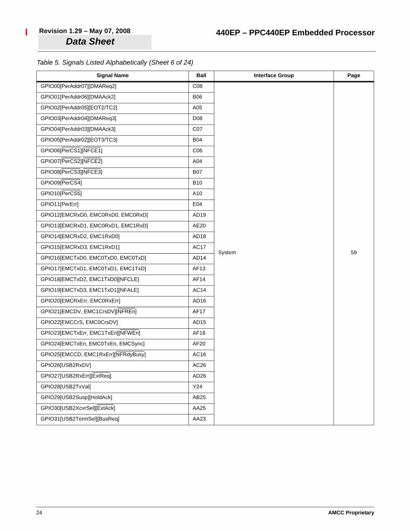
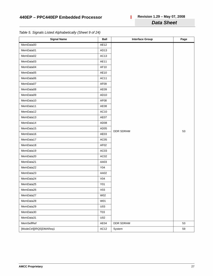
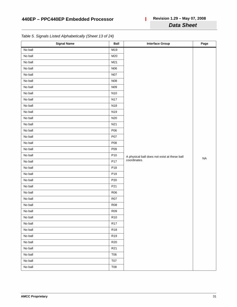
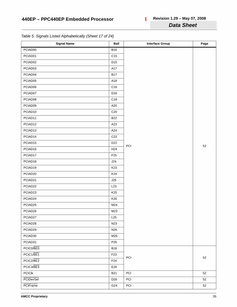
The following table lists all the external signals in alphabetical order and shows the ball (pin) number on which the signal appears. Multiplexed signals are shown with the default signal (following reset) not in brackets and alternate signals in brackets. Multiplexed signals appear alphabetically multiple times in the list—once for each signal name on the ball. The page number listed gives the page in “Signal Functional Description” on page 52 where the signals in the indicated interface group begin. In cases where signals in the same interface group (for example, Ethernet) have different names to distinguish variations in the mode of operation, the names are separated by a comma with the primary mode name appearing first. These signals are listed only once, and appear alphabetically by the primary mode name.
Table 5. Signals Listed Alphabetically (Sheet 1 of 24)
Signal Name Ball Interface Group Page
AGND AE17Power 60
AVDD AD17
BA0 AF03DDR SDRAM 53
BA1 AF04
BankSel0 R04
DDR SDRAM 53BankSel1 R02
BankSel2 R01
BankSel3 N01
[BusReq][USB2TermSel]GPIO31 AA23 External Master Peripheral 56
CAS J02 DDR SDRAM 53
ClkEn AF05 DDR SDRAM 53
DM0 AE05
DDR SDRAM 53
DM1 AD07
DM2 J01
DM3 L03
DM8 AF07
[DMAAck0][IRQ8]GPIO47 D18
External Slave Peripheral 55[DMAAck1][IRQ4]GPIO44 G25
[DMAAck2][PerAddr06]GPIO01 B06
[DMAAck3][PerAddr03]GPIO04 C07
[DMAReq0][IRQ7]GPIO46 B24
External Slave Peripheral 55DMAReq1[IRQ5][ModeCtrl] AC12
[DMAReq2][PerAddr07]GPIO00 C08
[DMAReq3][PerAddr04]GPIO03 D08
DQS0 AD09
DDR SDRAM 53
DQS1 AC08
DQS2 K03
DQS3 M04
DQS8 AC06
[DrvrInh1]USB2LS0[RejectPkt] Y25System 59
[DrvrInh2]Halt C25

20 AMCC Proprietary
440EP – PPC440EP Embedded ProcessorRevision 1.29 – May 07, 2008Data Sheet
ECC0 P02
DDR SDRAM 53
ECC1 N02
ECC2 M01
ECC3 M02
ECC4 N03
ECC5 N04
ECC6 L02
ECC7 M03
[EMCCD, EMC1RxErr]GPIO25[NFRdyBusy] AC16
Ethernet 54
[EMCCrS, EMC0CrsDV]GPIO22 AD15
[EMCDV, EMC1CrsDV]GPIO21[NFREn] AF17
EMCMDClk AE16
EMCMDIO AC18
EMCRxClk AF19
[EMCRxD0, EMC0RxD0, EMC0RxD]GPIO12 AD19
[EMCRxD1, EMC0RxD1, EMC1RxD]GPIO13 AE20
[EMCRxD2, EMC1RxD0]GPIO14 AD18
[EMCRxD3, EMC1RxD1]GPIO15 AC17
[EMCRxErr, EMC0RxErr]GPIO20 AD16
EMCTxClk, EMCRefClk AC15
[EMCTxD0, EMC0TxD0, EMC0TxD]GPIO16 AD14
[EMCTxD1, EMC0TxD1, EMC1TxD]GPIO17 AF13
[EMCTxD2, EMC1TxD0]GPIO18[NFCLE] AF14
[EMCTxD3, EMC1TxD1]GPIO19[NFALE] AC14
[EMCTxEn, EMC0TxEn, EMCSync]GPIO24 AF20
[EMCTxErr, EMC1TxEn]GPIO23[NFWEn] AF18
[EOT0/TC0][IRQ9]GPIO48 A19
External Slave Peripheral 55[EOT1/TC1][IRQ6]GPIO45 H23
[EOT2/TC2][PerAddr05]GPIO02 A05
[EOT3/TC3][PerAddr02]GPIO05 B04
[ExtAck][USB2XcvrSel]GPIO30 AA25 External Master Peripheral 56
[ExtReq][USB2RxErr]GPIO27 AD26 External Master Peripheral 56
ExtReset B23 External Master Peripheral 56
Table 5. Signals Listed Alphabetically (Sheet 2 of 24)
Signal Name Ball Interface Group Page

AMCC Proprietary 21
440EP – PPC440EP Embedded ProcessorData Sheet
Revision 1.29 – May 07, 2008
GND A01
Power 60
GND A02
GND A06
GND A09
GND A11
GND A16
GND A21
GND A26
GND B02
GND B25
GND B26
GND C03
GND C24
GND D04
GND D21
GND D23
GND E09
GND E14
GND E18
GND F01
GND F26
GND J05
GND J22
GND J26
GND L01
GND L04
GND L11
GND L13
GND L14
GND L16
GND L26
GND M12
GND M13
Table 5. Signals Listed Alphabetically (Sheet 3 of 24)
Signal Name Ball Interface Group Page

22 AMCC Proprietary
440EP – PPC440EP Embedded ProcessorRevision 1.29 – May 07, 2008Data Sheet
GND M15
Power 60
GND M25
GND N05
GND N11
GND N13
GND N14
GND N15
GND N16
GND P11
GND P12
GND P13
GND P14
GND P16
GND P22
GND R12
GND R14
GND R15
GND T01
GND T11
GND T13
GND T14
GND T16
GND T26
GND V05
GND V01
GND V22
GND AA01
GND AA26
GND AB09
GND AB13
GND AB18
GND AC01
GND AC04
GND AC07
GND AC23
Table 5. Signals Listed Alphabetically (Sheet 4 of 24)
Signal Name Ball Interface Group Page

AMCC Proprietary 23
440EP – PPC440EP Embedded ProcessorData Sheet
Revision 1.29 – May 07, 2008
GND AD03
Power 60
GND AD24
GND AE01
GND AE02
GND AE25
GND AF01
GND AF06
GND AF11
GND AF16
GND AF21
GND AF25
GND AF26
Table 5. Signals Listed Alphabetically (Sheet 5 of 24)
Signal Name Ball Interface Group Page
24 AMCC Proprietary
440EP – PPC440EP Embedded ProcessorRevision 1.29 – May 07, 2008Data Sheet
GPIO00[PerAddr07][DMAReq2] C08
System 59
GPIO01[PerAddr06][DMAAck2] B06
GPIO02[PerAddr05][EOT2/TC2] A05
GPIO03[PerAddr04][DMAReq3] D08
GPIO04[PerAddr03][DMAAck3] C07
GPIO05[PerAddr02][EOT3/TC3] B04
GPIO06[PerCS1][NFCE1] C06
GPIO07[PerCS2][NFCE2] A04
GPIO08[PerCS3][NFCE3] B07
GPIO09[PerCS4] B10
GPIO10[PerCS5] A10
GPIO11[PerErr] E04
GPIO12[EMCRxD0, EMC0RxD0, EMC0RxD] AD19
GPIO13[EMCRxD1, EMC0RxD1, EMC1RxD] AE20
GPIO14[EMCRxD2, EMC1RxD0] AD18
GPIO15[EMCRxD3, EMC1RxD1] AC17
GPIO16[EMCTxD0, EMC0TxD0, EMC0TxD] AD14
GPIO17[EMCTxD1, EMC0TxD1, EMC1TxD] AF13
GPIO18[EMCTxD2, EMC1TxD0][NFCLE] AF14
GPIO19[EMCTxD3, EMC1TxD1][NFALE] AC14
GPIO20[EMCRxErr, EMC0RxErr] AD16
GPIO21[EMCDV, EMC1CrsDV][NFREn] AF17
GPIO22[EMCCrS, EMC0CrsDV] AD15
GPIO23[EMCTxErr, EMC1TxEn][NFWEn] AF18
GPIO24[EMCTxEn, EMC0TxEn, EMCSync] AF20
GPIO25[EMCCD, EMC1RxErr][NFRdyBusy] AC16
GPIO26[USB2RxDV] AC26
GPIO27[USB2RxErr][ExtReq] AD26
GPIO28[USB2TxVal] Y24
GPIO29[USB2Susp][HoldAck] AB25
GPIO30[USB2XcvrSel][ExtAck] AA25
GPIO31[USB2TermSel][BusReq] AA23
Table 5. Signals Listed Alphabetically (Sheet 6 of 24)
Signal Name Ball Interface Group Page

AMCC Proprietary 25
440EP – PPC440EP Embedded ProcessorData Sheet
Revision 1.29 – May 07, 2008
GPIO32[USB2OM0] W24
System 59
GPIO33[USB2OM1] AB26
GPIO34[UART0_DCD/UART1_CTS/UART2_Tx] R25
GPIO35[UART0_DSR/UART1_RTS/UART2_Rx] U26
GPIO36[UART0_CTS/UART3_Rx] V26
GPIO37[UART0_RTS/UART3_Tx] R26
GPIO38[UART0_DTR/UART1_Tx] N24
GPIO39[UART0_RI/UART1_Rx] P24
GPIO40[IRQ0] D03
GPIO41[IRQ1] G04
GPIO42[IRQ2] F02
GPIO43[IRQ3] G02
GPIO44[IRQ4][DMAAck1] G25
GPIO45[IRQ6][EOT1/TC1] H23
GPIO46[IRQ7][DMAReq0] B24
GPIO47[IRQ8][DMAAck0] D18
GPIO48[IRQ9][EOT0/TC0] A19
GPIO49[TrcBS0] AE21
GPIO50[TrcBS1] AC25
GPIO51[TrcBS2] AA24
GPIO52[TrcES0] Y03
GPIO53[TrcES1] AA04
GPIO54[TrcES2] AB03
GPIO55[TrcES3] AB04
GPIO56[TrcES4] AF22
GPIO57[TrcTS0] AC22
GPIO58[TrcTS1] AE24
GPIO59[TrcTS2] AD04
GPIO60[TrcTS3] AD06
GPIO61[TrcTS4] AC09
GPIO62[TrcTS5] AD12
GPIO63[TrcTS6] AE15
Halt[DrvrInh2] C25 System 59
[HoldAck][USB2Susp]GPIO29 AB25
External Master Peripheral 56[HoldPri]USB2LS1[LeakTest] V24
[HoldReq]USB2RxAct[RcvrInh] Y23
IIC0SClk U25IIC0 Peripheral 56
IIC0SData T24
Table 5. Signals Listed Alphabetically (Sheet 7 of 24)
Signal Name Ball Interface Group Page

26 AMCC Proprietary
440EP – PPC440EP Embedded ProcessorRevision 1.29 – May 07, 2008Data Sheet
[IIC1SClk]SCPClkOut U24IIC1 Peripheral 56
[IIC1SData]SCPDI V25
[IRQ0]GPIO40 D03
Interrupts 58
[IRQ1]GPIO41 G04
[IRQ2]GPIO42 F02
[IRQ3]GPIO43 G02
[IRQ4]GPIO44[DMAAck1] G25
[IRQ5][ModeCtrl]DMAReq1 AC12
[IRQ6]GPIO45[EOT1/TC1] H23
[IRQ7]GPIO46[DMAReq0] B24
[IRQ8]GPIO47[DMAAck0] D18
[IRQ9]GPIO48[EOT0/TC0] A19
[LeakTest]USB2LS1[HoldPri] V24 System 59
MemAddr00 P01
DDR SDRAM 53
MemAddr01 P04
MemAddr02 T02
MemAddr03 T04
MemAddr04 U01
MemAddr05 V02
MemAddr06 U04
MemAddr07 W03
MemAddr08 Y02
MemAddr09 AB02
MemAddr10 R03
MemAddr11 AD01
MemAddr12 AD02
MemClkOut0 AF12DDR SDRAM 53
MemClkOut0 AE13
Table 5. Signals Listed Alphabetically (Sheet 8 of 24)
Signal Name Ball Interface Group Page
AMCC Proprietary 27
440EP – PPC440EP Embedded ProcessorData Sheet
Revision 1.29 – May 07, 2008
MemData00 AE12
DDR SDRAM 53
MemData01 AD13
MemData02 AC13
MemData03 AE11
MemData04 AF10
MemData05 AE10
MemData06 AC11
MemData07 AF09
MemData08 AE09
MemData09 AD10
MemData10 AF08
MemData11 AE08
MemData12 AC10
MemData13 AE07
MemData14 AD08
MemData15 AD05
MemData16 AE03
MemData17 AC05
MemData18 AF02
MemData19 AC03
MemData20 AC02
MemData21 AA03
MemData22 Y04
MemData23 AA02
MemData24 V04
MemData25 Y01
MemData26 V03
MemData27 W02
MemData28 W01
MemData29 U03
MemData30 T03
MemData31 U02
MemSelfRef AE04 DDR SDRAM 53
[ModeCtrl][IRQ5]DMAReq1 AC12 System 59
Table 5. Signals Listed Alphabetically (Sheet 9 of 24)
Signal Name Ball Interface Group Page

28 AMCC Proprietary
440EP – PPC440EP Embedded ProcessorRevision 1.29 – May 07, 2008Data Sheet
[NFALE][EMCTxD3, EMC1TxD1]GPIO19 AC14
NAND Flash 58
[NFCE0]PerCS0 D06
[NFCE1][PerCS1]GPIO06 C06
[NFCE2][PerCS2]GPIO07 A04
[NFCE3][PerCS3]GPIO08 B07
[NFCLE][EMCTxD2, EMC1TxD0]GPIO18 AF14
[NFRdyBusy][EMCCD, EMC1RxErr]GPIO25 AC16
[NFREn][EMCDV, EMC1CrsDV]GPIO21 AF17
[NFWEn][EMCTxErr, EMC1TxEn]GPIO23 AF18
No ball F06
A physical ball does not exist at these ball coordinates. NA
No ball F07
No ball F08
No ball F09
No ball F10
No ball F11
No ball F12
No ball F13
No ball F14
No ball F15
No ball F16
No ball F17
No ball F18
No ball F19
No ball F20
No ball F21
No ball G06
No ball G07
No ball G08
No ball G09
No ball G10
No ball G11
No ball G12
No ball G13
No ball G14
No ball G15
Table 5. Signals Listed Alphabetically (Sheet 10 of 24)
Signal Name Ball Interface Group Page

AMCC Proprietary 29
440EP – PPC440EP Embedded ProcessorData Sheet
Revision 1.29 – May 07, 2008
No ball G16
A physical ball does not exist at these ball coordinates. NA
No ball G17
No ball G18
No ball G19
No ball G20
No ball G21
No ball H06
No ball H07
No ball H08
No ball H09
No ball H10
No ball H11
No ball H12
No ball H13
No ball H14
No ball H15
No ball H16
No ball H17
No ball H18
No ball H19
No ball H20
No ball H21
No ball J06
No ball J07
No ball J08
No ball J09
No ball J10
No ball J11
No ball J12
No ball J13
No ball J14
No ball J15
No ball J16
No ball J17
No ball J18
No ball J19
Table 5. Signals Listed Alphabetically (Sheet 11 of 24)
Signal Name Ball Interface Group Page

30 AMCC Proprietary
440EP – PPC440EP Embedded ProcessorRevision 1.29 – May 07, 2008Data Sheet
No ball J20
A physical ball does not exist at these ball coordinates. NA
No ball J21
No ball K06
No ball K07
No ball K08
No ball K09
No ball K10
No ball K11
No ball K12
No ball K13
No ball K14
No ball K15
No ball K16
No ball K17
No ball K18
No ball K19
No ball K20
No ball K21
No ball L06
No ball L07
No ball L08
No ball L09
No ball L10
No ball L17
No ball L18
No ball L19
No ball L20
No ball L21
No ball M06
No ball M07
No ball M08
No ball M09
No ball M10
No ball M17
No ball M18
Table 5. Signals Listed Alphabetically (Sheet 12 of 24)
Signal Name Ball Interface Group Page
AMCC Proprietary 31
440EP – PPC440EP Embedded ProcessorData Sheet
Revision 1.29 – May 07, 2008
No ball M19
A physical ball does not exist at these ball coordinates. NA
No ball M20
No ball M21
No ball N06
No ball N07
No ball N08
No ball N09
No ball N10
No ball N17
No ball N18
No ball N19
No ball N20
No ball N21
No ball P06
No ball P07
No ball P08
No ball P09
No ball P10
No ball P17
No ball P18
No ball P19
No ball P20
No ball P21
No ball R06
No ball R07
No ball R08
No ball R09
No ball R10
No ball R17
No ball R18
No ball R19
No ball R20
No ball R21
No ball T06
No ball T07
No ball T08
Table 5. Signals Listed Alphabetically (Sheet 13 of 24)
Signal Name Ball Interface Group Page

32 AMCC Proprietary
440EP – PPC440EP Embedded ProcessorRevision 1.29 – May 07, 2008Data Sheet
No ball T09
A physical ball does not exist at these ball coordinates. NA
No ball T10
No ball T17
No ball T18
No ball T19
No ball T20
No ball T21
No ball U06
No ball U07
No ball U08
No ball U09
No ball U10
No ball U11
No ball U12
No ball U13
No ball U14
No ball U15
No ball U16
No ball U17
No ball U18
No ball U19
No ball U20
No ball U21
No ball V06
No ball V07
No ball V08
No ball V09
No ball V10
No ball V11
No ball V12
No ball V13
No ball V14
No ball V15
No ball V16
No ball V17
Table 5. Signals Listed Alphabetically (Sheet 14 of 24)
Signal Name Ball Interface Group Page

AMCC Proprietary 33
440EP – PPC440EP Embedded ProcessorData Sheet
Revision 1.29 – May 07, 2008
No ball V18
A physical ball does not exist at these ball coordinates. NA
No ball V19
No ball V20
No ball V21
No ball W06
No ball W07
No ball W08
No ball W09
No ball W10
No ball W11
No ball W12
No ball W13
No ball W14
No ball W15
No ball W16
No ball W17
No ball W18
No ball W19
No ball W20
No ball W21
No ball Y06
No ball Y07
No ball Y08
No ball Y09
No ball Y10
No ball Y11
No ball Y12
No ball Y13
No ball Y14
No ball Y15
No ball Y16
No ball Y17
No ball Y18
No ball Y19
No ball Y20
No ball Y21
Table 5. Signals Listed Alphabetically (Sheet 15 of 24)
Signal Name Ball Interface Group Page

34 AMCC Proprietary
440EP – PPC440EP Embedded ProcessorRevision 1.29 – May 07, 2008Data Sheet
No ball AA06
A physical ball does not exist at these ball coordinates. NA
No ball AA07
No ball AA08
No ball AA09
No ball AA10
No ball AA11
No ball AA12
No ball AA13
No ball AA14
No ball AA15
No ball AA16
No ball AA17
No ball AA18
No ball AA19
No ball AA20
No ball AA21
OVDD E06
Power 60
OVDD E07
OVDD E08
OVDD E13
OVDD E19
OVDD E20
OVDD E21
OVDD F05
OVDD F22
OVDD G05
OVDD G22
OVDD H05
OVDD H22
OVDD L12
OVDD L15
OVDD M11
OVDD M16
OVDD N22
Table 5. Signals Listed Alphabetically (Sheet 16 of 24)
Signal Name Ball Interface Group Page
AMCC Proprietary 35
440EP – PPC440EP Embedded ProcessorData Sheet
Revision 1.29 – May 07, 2008
PCIAD00 B16
PCI 52
PCIAD01 C15
PCIAD02 D15
PCIAD03 A17
PCIAD04 B17
PCIAD05 A18
PCIAD06 C16
PCIAD07 D16
PCIAD08 C18
PCIAD09 A20
PCIAD10 C20
PCIAD11 B22
PCIAD12 A23
PCIAD13 A24
PCIAD14 C22
PCIAD15 D22
PCIAD16 H24
PCIAD17 F25
PCIAD18 J24
PCIAD19 K23
PCIAD20 K24
PCIAD21 J25
PCIAD22 L23
PCIAD23 K25
PCIAD24 K26
PCIAD25 M24
PCIAD26 M23
PCIAD27 L25
PCIAD28 N23
PCIAD29 N26
PCIAD30 M26
PCIAD31 P26
PCIC0/BE0 B18
PCI 52PCIC1/BE1 F23
PCIC2/BE2 F24
PCIC3/BE3 E26
PCIClk B21 PCI 52
PCIDevSel D26 PCI 52
PCIFrame G24 PCI 52
Table 5. Signals Listed Alphabetically (Sheet 17 of 24)
Signal Name Ball Interface Group Page

36 AMCC Proprietary
440EP – PPC440EP Embedded ProcessorRevision 1.29 – May 07, 2008Data Sheet
PCIGnt0/Req D17
PCI 52
PCIGnt1 L24
PCIGnt2 A25
PCIGnt3 D25
PCIGnt4 H25
PCIGnt5 E24
PCIIDSel G26 PCI 52
PCIINT D20 PCI 52
PCIIRDY E25 PCI 52
PCIPar C23 PCI 52
PCIPErr D24 PCI 52
PCIReq0/Gnt N25
PCI 52
PCIReq1 B20
PCIReq2 B19
PCIReq3 C19
PCIReq4 A22
PCIReq5 H26
PCIReset D19 PCI 52
PCISErr J23 PCI 52
PCIStop E23 PCI 52
PCITRDY G23 PCI 52
Table 5. Signals Listed Alphabetically (Sheet 18 of 24)
Signal Name Ball Interface Group Page

AMCC Proprietary 37
440EP – PPC440EP Embedded ProcessorData Sheet
Revision 1.29 – May 07, 2008
[PerAddr02]GPIO05[EOT3/TC3] B04
External Slave Peripheral 55
[PerAddr03]GPIO04[DMAAck3] C07
[PerAddr04]GPIO03[DMAReq3] D08
[PerAddr05]GPIO02[EOT2/TC2] A05
[PerAddr06]GPIO01[DMAAck2] B06
[PerAddr07]GPIO00[DMAReq2] C08
PerAddr08 D09
PerAddr09 A07
PerAddr10 C09
PerAddr11 B08
PerAddr12 D10
PerAddr13 A08
PerAddr14 B09
PerAddr15 C10
PerAddr16 C11
PerAddr17 D12
PerAddr18 C12
PerAddr19 B11
PerAddr20 B12
PerAddr21 D13
PerAddr22 A13
PerAddr23 A12
PerAddr24 A14
PerAddr25 B13
PerAddr26 C13
PerAddr27 B14
PerAddr28 A15
PerAddr29 B15
PerAddr30 C14
PerAddr31 D14
PerBLast D11 External Slave Peripheral 55
PerClk C02 External Master Peripheral 56
PerCS0[NFCE0] D06
External Slave Peripheral 55
[PerCS1][NFCE1]GPIO06 C06
[PerCS2][NFCE2]GPIO07 A04
[PerCS3][NFCE3]GPIO08 B07
[PerCS4]GPIO09 B10
[PerCS5]GPIO10 A10
Table 5. Signals Listed Alphabetically (Sheet 19 of 24)
Signal Name Ball Interface Group Page

38 AMCC Proprietary
440EP – PPC440EP Embedded ProcessorRevision 1.29 – May 07, 2008Data Sheet
PerData00 H01
External Slave Peripheral 55
PerData01 K04
PerData02 G01
PerData03 J03
PerData04 J04
PerData05 H03
PerData06 E01
PerData07 G03
PerData08 H04
PerData09 E02
PerData10 D01
PerData11 F03
PerData12 C01
PerData13 F04
PerData14 E03
PerData15 B01
[PerErr]GPIO11 E04 External Master Peripheral 55
PerOE B03 External Slave Peripheral 55
PerReady C05 External Slave Peripheral 55
PerR/W D05 External Slave Peripheral 55
PerWBE0 H02External Slave Peripheral 55
PerWBE1 C04
PSROOut C26 System 59
RAS K02 DDR SDRAM 53
[RcvrInh]USB2RxAct[HoldReq] Y23 System 59
[RefEn]USB2TxRdy W23 System 59
[RejectPkt]USB2LS0[DrvrInh1] Y25 Ethernet 54
SAGND AF15Power 60
SAVDD AE14
SCPClkOut[IIC1SClk] U24
Serial Peripheral (SPI) 58SCPDI[IIC1SData] V25
SCPDO T23
Table 5. Signals Listed Alphabetically (Sheet 20 of 24)
Signal Name Ball Interface Group Page

AMCC Proprietary 39
440EP – PPC440EP Embedded ProcessorData Sheet
Revision 1.29 – May 07, 2008
SVDD P05
Power 60
SVDD R11
SVDD R16
SVDD T12
SVDD T15
SVDD W05
SVDD W22
SVDD Y05
SVDD Y22
SVDD AA05
SVDD AA22
SVDD AB06
SVDD AB07
SVDD AB08
SVDD AB14
SVDD AB19
SVDD AB20
SVDD AB21
SVREF1 W04
DDR SDRAM 53SVREF2A P03
SVREF2B AE06
SysClk AE19 System 59
SysErr AB01 System 59
SysReset AE18 System 59
TCK B05 JTAG 58
TDI C17 JTAG 58
TDO C21 JTAG 58
TestEn A03 System 59
TmrClk AD11 System 59
TMS D02 JTAG 58
[TrcBS0]GPIO49 AE21
Trace 60[TrcBS1]GPIO50 AC25
[TrcBS2]GPIO51 AA24
TrcClk AC19 Trace 60
Table 5. Signals Listed Alphabetically (Sheet 21 of 24)
Signal Name Ball Interface Group Page

40 AMCC Proprietary
440EP – PPC440EP Embedded ProcessorRevision 1.29 – May 07, 2008Data Sheet
[TrcES0]GPIO52 Y03
Trace 60
[TrcES1]GPIO53 AA04
[TrcES2]GPIO54 AB03
[TrcES3]GPIO55 AB04
[TrcES4]GPIO56 AF22
[TrcTS0]GPIO57 AC22
Trace 60
[TrcTS1]GPIO58 AE24
[TrcTS2]GPIO59 AD04
[TrcTS3]GPIO60 AD06
[TrcTS4]GPIO61 AC09
[TrcTS5]GPIO62 AD12
[TrcTS6]GPIO63 AE15
TRST D07 JTAG 58
[UART0_CTS/UART3_Rx]GPIO36 V26
UART Peripheral 56
[UART0_RTS/UART3_Tx]GPIO37 R26
UART0_Rx T25
UART0_Tx P25
[UART0_DCD/UART1_CTS/UART2_Tx]GPIO34 R25
[UART0_DSR/UART1_RTS/UART2_Rx]GPIO35 U26
[UART0_DTR/UART1_Tx]GPIO38 N24
[UART0_RI/UART1_Rx]GPIO39 P24
UARTSerClk P23
Table 5. Signals Listed Alphabetically (Sheet 22 of 24)
Signal Name Ball Interface Group Page

AMCC Proprietary 41
440EP – PPC440EP Embedded ProcessorData Sheet
Revision 1.29 – May 07, 2008
USB1Clk AD25
Universal Serial Bus 57
USB1DevXcvr R23
USB1DevXcvr R24
USB1HostXcvr W25
USB1HostXcvr W26
USB2Clk AD22
USB2DI0 AD21
USB2DI1 AE23
USB2DI2 AF24
USB2DI3 AC21
USB2DI4 AE26
USB2DI5 AB23
USB2DI6 AC24
USB2DI7 AB24
USB2DO0 AD20
USB2DO1 AE22
USB2DO2 AC20
USB2DO3 AF23
USB2DO4 AD23
USB2DO5 V23
USB2DO6 Y26
USB2DO7 U23
USB2LS0[DrvrInh1][RejectPkt] Y25
USB2LS1[LeakTest][HoldPri] V24
[USB2OM0]GPIO32 W24
[USB2OM1]GPIO33 AB26
USB2RxAct[HoldReq][RcvrInh] Y23
[USB2RxDV]GPIO26 AC26
[USB2RxErr]GPIO27[ExtReq] AD26
[USB2Susp]GPIO29[HoldAck] AB25
[USB2TermSel]GPIO31[BusReq] AA23
USB2TxRdy[RefEn] W23
[USB2TxVal]GPIO28 Y24
[USB2XcvrSel]GPIO30[ExtAck] AA25
Table 5. Signals Listed Alphabetically (Sheet 23 of 24)
Signal Name Ball Interface Group Page

42 AMCC Proprietary
440EP – PPC440EP Embedded ProcessorRevision 1.29 – May 07, 2008Data Sheet
VDD E05
Power 60
VDD E10
VDD E11
VDD E12
VDD E15
VDD E16
VDD E17
VDD E22
VDD K05
VDD K22
VDD L05
VDD L22
VDD M05
VDD M22
VDD M14
VDD N12
VDD P15
VDD R05
VDD R13
VDD R22
VDD T05
VDD T22
VDD U05
VDD U22
VDD AB05
VDD AB10
VDD AB11
VDD AB12
VDD AB15
VDD AB16
VDD AB17
VDD AB22
WE K01 DDR SDRAM 53
Table 5. Signals Listed Alphabetically (Sheet 24 of 24)
Signal Name Ball Interface Group Page

AMCC Proprietary 43
440EP – PPC440EP Embedded ProcessorData Sheet
Revision 1.29 – May 07, 2008
In the following table, only the primary (default) signal name is shown for each pin. Multiplexed or multifunction signals are marked with an asterisk (*). To determine what signals or functions are multiplexed on those pins, look up the primary signal name in Table 5, Signals Listed Alphabetically.
Table 6. Signals Listed by Ball Assignment (Sheet 1 of 7)
Ball Signal Name Ball Signal Name Ball Signal Name Ball Signal Name
A01 GND B01 PerData15 C01 PerData12 D01 PerData10
A02 GND B02 GND C02 PerClk D02 TMS
A03 TestEn B03 PerOE C03 GND D03 GPIO40*
A04 GPIO07* B04 GPIO05* C04 PerWBE1 D04 GND
A05 GPIO02* B05 TCK C05 PerReady D05 PerR/W
A06 GND B06 GPIO01* C06 GPIO06* D06 PerCS0
A07 PerAddr09 B07 GPIO08* C07 GPIO04* D07 TRST
A08 PerAddr13 B08 PerAddr11 C08 GPIO00* D08 GPIO03*
A09 GND B09 PerAddr14 C09 PerAddr10 D09 PerAddr08
A10 GPIO10* B10 GPIO09* C10 PerAddr15 D10 PerAddr12
A11 GND B11 PerAddr19 C11 PerAddr16 D11 PerBLast
A12 PerAddr23 B12 PerAddr20 C12 PerAddr18 D12 PerAddr17
A13 PerAddr22 B13 PerAddr25* C13 PerAddr26* D13 PerAddr21
A14 PerAddr24* B14 PerAddr27* C14 PerAddr30 D14 PerAddr31
A15 PerAddr28* B15 PerAddr29* C15 PCIAD01 D15 PCIAD02
A16 GND B16 PCIAD00 C16 PCIAD06 D16 PCIAD07
A17 PCIAD03 B17 PCIAD04 C17 TDI D17 PCIGnt0/Req
A18 PCIAD05 B18 PCIC0/BE0 C18 PCIAD08 D18 GPIO47*
A19 GPIO48* B19 PCIReq2 C19 PCIReq3 D19 PCIReset
A20 PCIAD09 B20 PCIReq1 C20 PCIAD10 D20 PCIINT
A21 GND B21 PCIClk C21 TDO D21 GND
A22 PCIReq4 B22 PCIAD11 C22 PCIAD14 D22 PCIAD15
A23 PCIAD12 B23 ExtReset C23 PCIPar D23 GND
A24 PCIAD13 B24 GPIO46* C24 GND D24 PCIPErr
A25 PCIGnt2 B25 GND C25 Halt[DrvrInh2] D25 PCIGnt3
A26 GND B26 GND C26 PSROOut D26 PCIDevSel

44 AMCC Proprietary
440EP – PPC440EP Embedded ProcessorRevision 1.29 – May 07, 2008Data Sheet
E01 PerData06 F01 GND G01 PerData02 H01 PerData00
E02 PerData09 F02 GPIO42* G02 GPIO43* H02 PerWBE0
E03 PerData14 F03 PerData11 G03 PerData07 H03 PerData05
E04 GPIO11* F04 PerData13 G04 GPIO41* H04 PerData08
E05 VDD F05 OVDD G05 OVDD H05 OVDD
E06 OVDD F06 No ball G06 No ball H06 No ball
E07 OVDD F07 No ball G07 No ball H07 No ball
E08 OVDD F08 No ball G08 No ball H08 No ball
E09 GND F09 No ball G09 No ball H09 No ball
E10 VDD F10 No ball G10 No ball H10 No ball
E11 VDD F11 No ball G11 No ball H11 No ball
E12 VDD F12 No ball G12 No ball H12 No ball
E13 OVDD F13 No ball G13 No ball H13 No ball
E14 GND F14 No ball G14 No ball H14 No ball
E15 VDD F15 No ball G15 No ball H15 No ball
E16 VDD F16 No ball G16 No ball H16 No ball
E17 VDD F17 No ball G17 No ball H17 No ball
E18 GND F18 No ball G18 No ball H18 No ball
E19 OVDD F19 No ball G19 No ball H19 No ball
E20 OVDD F20 No ball G20 No ball H20 No ball
E21 OVDD F21 No ball G21 No ball H21 No ball
E22 VDD F22 OVDD G22 OVDD H22 OVDD
E23 PCIStop F23 PCIC1/BE1 G23 PCITRDY H23 GPIO45*
E24 PCIGnt5 F24 PCIC2/BE2 G24 PCIFrame H24 PCIAD16
E25 PCIIRDY F25 PCIAD17 G25 GPIO44* H25 PCIGnt4
E26 PCIC3/BE3 F26 GND G26 PCIIDSel H26 PCIReq5
Table 6. Signals Listed by Ball Assignment (Sheet 2 of 7)Ball Signal Name Ball Signal Name Ball Signal Name Ball Signal Name

AMCC Proprietary 45
440EP – PPC440EP Embedded ProcessorData Sheet
Revision 1.29 – May 07, 2008
J01 DM2 K01 WE L01 GND M01 ECC2
J02 CAS K02 RAS L02 ECC6 M02 ECC3
J03 PerData03 K03 DQS2 L03 DM3 M03 ECC7
J04 PerData04 K04 PerData01 L04 GND M04 DQS3
J05 GND K05 VDD L05 VDD M05 VDD
J06 No ball K06 No ball L06 No ball M06 No ball
J07 No ball K07 No ball L07 No ball M07 No ball
J08 No ball K08 No ball L08 No ball M08 No ball
J09 No ball K09 No ball L09 No ball M09 No ball
J10 No ball K10 No ball L10 No ball M10 No ball
J11 No ball K11 No ball L11 GND M11 OVDD
J12 No ball K12 No ball L12 OVDD M12 GND
J13 No ball K13 No ball L13 GND M13 GND
J14 No ball K14 No ball L14 GND M14 VDD
J15 No ball K15 No ball L15 OVDD M15 GND
J16 No ball K16 No ball L16 GND M16 OVDD
J17 No ball K17 No ball L17 No ball M17 No ball
J18 No ball K18 No ball L18 No ball M18 No ball
J19 No ball K19 No ball L19 No ball M19 No ball
J20 No ball K20 No ball L20 No ball M20 No ball
J21 No ball K21 No ball L21 No ball M21 No ball
J22 GND K22 VDD L22 VDD M22 VDD
J23 PCISErr K23 PCIAD19 L23 PCIAD22 M23 PCIAD26
J24 PCIAD18 K24 PCIAD20 L24 PCIGnt1 M24 PCIAD25
J25 PCIAD21 K25 PCIAD23 L25 PCIAD27 M25 GND
J26 GND K26 PCIAD24 L26 GND M26 PCIAD30
Table 6. Signals Listed by Ball Assignment (Sheet 3 of 7)Ball Signal Name Ball Signal Name Ball Signal Name Ball Signal Name

46 AMCC Proprietary
440EP – PPC440EP Embedded ProcessorRevision 1.29 – May 07, 2008Data Sheet
N01 BankSel3 P01 MemAddr00 R01 BankSel2 T01 GND
N02 ECC1 P02 ECC0 R02 BankSel1 T02 MemAddr02
N03 ECC4 P03 SVREF2A R03 MemAddr10 T03 MemData30
N04 ECC5 P04 MemAddr01 R04 BankSel0 T04 MemAddr03
N05 GND P05 SVDD R05 VDD T05 VDD
N06 No ball P06 No ball R06 No ball T06 No ball
N07 No ball P07 No ball R07 No ball T07 No ball
N08 No ball P08 No ball R08 No ball T08 No ball
N09 No ball P09 No ball R09 No ball T09 No ball
N10 No ball P10 No ball R10 No ball T10 No ball
N11 GND P11 GND R11 SVDD T11 GND
N12 VDD P12 GND R12 GND T12 SVDD
N13 GND P13 GND R13 VDD T13 GND
N14 GND P14 GND R14 GND T14 GND
N15 GND P15 VDD R15 GND T15 SVDD
N16 GND P16 GND R16 SVDD T16 GND
N17 No ball P17 No ball R17 No ball T17 No ball
N18 No ball P18 No ball R18 No ball T18 No ball
N19 No ball P19 No ball R19 No ball T19 No ball
N20 No ball P20 No ball R20 No ball T20 No ball
N21 No ball P21 No ball R21 No ball T21 No ball
N22 OVDD P22 GND R22 VDD T22 VDD
N23 PCIAD28 P23 UARTSerClk R23 USB1DevXcvr T23 SCPDO
N24 GPIO38* P24 GPIO39* R24 USB1DevXcvr T24 IIC0SData
N25 PCIReq0/Gnt P25 UART0_Tx R25 GPIO34* T25 UART0_Rx
N26 PCIAD29 P26 PCIAD31 R26 GPIO37* T26 GND
Table 6. Signals Listed by Ball Assignment (Sheet 4 of 7)Ball Signal Name Ball Signal Name Ball Signal Name Ball Signal Name

AMCC Proprietary 47
440EP – PPC440EP Embedded ProcessorData Sheet
Revision 1.29 – May 07, 2008
U01 MemAddr04 V01 GND W01 MemData28 Y01 MemData25
U02 MemData31 V02 MemAddr05 W02 MemData27 Y02 MemAddr08
U03 MemData29 V03 MemData26 W03 MemAddr07 Y03 GPIO52*
U04 MemAddr06 V04 MemData24 W04 SVREF1 Y04 MemData22
U05 VDD V05 GND W05 SVDD Y05 SVDD
U06 No ball V06 No ball W06 No ball Y06 No ball
U07 No ball V07 No ball W07 No ball Y07 No ball
U08 No ball V08 No ball W08 No ball Y08 No ball
U09 No ball V09 No ball W09 No ball Y09 No ball
U10 No ball V10 No ball W10 No ball Y10 No ball
U11 No ball V11 No ball W11 No ball Y11 No ball
U12 No ball V12 No ball W12 No ball Y12 No ball
U13 No ball V13 No ball W13 No ball Y13 No ball
U14 No ball V14 No ball W14 No ball Y14 No ball
U15 No ball V15 No ball W15 No ball Y15 No ball
U16 No ball V16 No ball W16 No ball Y16 No ball
U17 No ball V17 No ball W17 No ball Y17 No ball
U18 No ball V18 No ball W18 No ball Y18 No ball
U19 No ball V19 No ball W19 No ball Y19 No ball
U20 No ball V20 No ball W20 No ball Y20 No ball
U21 No ball V21 No ball W21 No ball Y21 No ball
U22 VDD V22 GND W22 SVDD Y22 SVDD
U23 USB2DO7 V23 USB2DO5 W23 USB2TxRdy* Y23 USB2RxAct*
U24 SCPClkOut* V24 USB2LS1* W24 GPIO32* Y24 GPIO28*
U25 IIC0SClk V25 SCPDI* W25 USB1HostXcvr Y25 USB2LS0*
U26 GPIO35* V26 GPIO36* W26 USB1HostXcvr Y26 USB2DO6
Table 6. Signals Listed by Ball Assignment (Sheet 5 of 7)Ball Signal Name Ball Signal Name Ball Signal Name Ball Signal Name

48 AMCC Proprietary
440EP – PPC440EP Embedded ProcessorRevision 1.29 – May 07, 2008Data Sheet
AA01 GND AB01 SysErr AC01 GND AD01 MemAddr11
AA02 MemData23 AB02 MemAddr09 AC02 MemData20 AD02 MemAddr12
AA03 MemData21 AB03 GPIO54* AC03 MemData19 AD03 GND
AA04 GPIO53* AB04 GPIO55* AC04 GND AD04 GPIO59*
AA05 SVDD AB05 VDD AC05 MemData17 AD05 MemData15
AA06 No ball AB06 SVDD AC06 DQS8 AD06 GPIO60*
AA07 No ball AB07 SVDD AC07 GND AD07 DM1
AA08 No ball AB08 SVDD AC08 DQS1 AD08 MemData14
AA09 No ball AB09 GND AC09 GPIO61* AD09 DQS0
AA10 No ball AB10 VDD AC10 MemData12 AD10 MemData09
AA11 No ball AB11 VDD AC11 MemData06 AD11 TmrClk
AA12 No ball AB12 VDD AC12 IRQ5* AD12 GPIO62*
AA13 No ball AB13 GND AC13 MemData02 AD13 MemData01
AA14 No ball AB14 SVDD AC14 GPIO19* AD14 GPIO16*
AA15 No ball AB15 VDD AC15 EMCTxClk* AD15 GPIO22*
AA16 No ball AB16 VDD AC16 GPIO25* AD16 GPIO20*
AA17 No ball AB17 VDD AC17 GPIO15* AD17 AVDD
AA18 No ball AB18 GND AC18 EMCMDIO AD18 GPIO14*
AA19 No ball AB19 SVDD AC19 TrcClk AD19 GPIO12*
AA20 No ball AB20 SVDD AC20 USB2DO2 AD20 USB2DO0
AA21 No ball AB21 SVDD AC21 USB2DI3 AD21 USB2DI0
AA22 SVDD AB22 VDD AC22 GPIO57* AD22 USB2Clk
AA23 GPIO31* AB23 USB2DI5 AC23 GND AD23 USB2DO4
AA24 GPIO51* AB24 USB2DI7 AC24 USB2DI6 AD24 GND
AA25 GPIO30* AB25 GPIO29* AC25 GPIO50* AD25 USB1Clk
AA26 GND AB26 GPIO33* AC26 GPIO26* AD26 GPIO27*
Table 6. Signals Listed by Ball Assignment (Sheet 6 of 7)Ball Signal Name Ball Signal Name Ball Signal Name Ball Signal Name

AMCC Proprietary 49
440EP – PPC440EP Embedded ProcessorData Sheet
Revision 1.29 – May 07, 2008
AE01 GND AF01 GND
AE02 GND AF02 MemData18
AE03 MemData16 AF03 BA0
AE04 MemSelfRef AF04 BA1
AE05 DM0 AF05 ClkEn
AE06 SVREF2B AF06 GND
AE07 MemData13 AF07 DM8
AE08 MemData11 AF08 MemData10
AE09 MemData08 AF09 MemData07
AE10 MemData05 AF10 MemData04
AE11 MemData03 AF11 GND
AE12 MemData00 AF12 MemClkOut0
AE13 MemClkOut0 AF13 GPIO17*
AE14 SAVDD AF14 GPIO18*
AE15 GPIO63* AF15 SAGND
AE16 EMCMDClk AF16 GND
AE17 AGND AF17 GPIO21*
AE18 SysReset AF18 GPIO23*
AE19 SysClk AF19 EMCRxClk
AE20 GPIO13* AF20 GPIO24*
AE21 GPIO49* AF21 GND
AE22 USB2DO1 AF22 GPIO56*
AE23 USB2DI1 AF23 USB2DO3
AE24 GPIO58* AF24 USB2DI2
AE25 GND AF25 GND
AE26 USB2DI4 AF26 GND
Table 6. Signals Listed by Ball Assignment (Sheet 7 of 7)Ball Signal Name Ball Signal Name Ball Signal Name Ball Signal Name
50 AMCC Proprietary
440EP – PPC440EP Embedded ProcessorRevision 1.29 – May 07, 2008Data Sheet
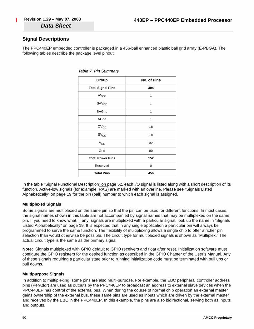
Signal Descriptions
The PPC440EP embedded controller is packaged in a 456-ball enhanced plastic ball grid array (E-PBGA). The following tables describe the package level pinout.
In the table “Signal Functional Description” on page 52, each I/O signal is listed along with a short description of its function. Active-low signals (for example, RAS) are marked with an overline. Please see “Signals Listed Alphabetically” on page 19 for the pin (ball) number to which each signal is assigned.
Multiplexed SignalsSome signals are multiplexed on the same pin so that the pin can be used for different functions. In most cases, the signal names shown in this table are not accompanied by signal names that may be multiplexed on the same pin. If you need to know what, if any, signals are multiplexed with a particular signal, look up the name in “Signals Listed Alphabetically” on page 19. It is expected that in any single application a particular pin will always be programmed to serve the same function. The flexibility of multiplexing allows a single chip to offer a richer pin selection than would otherwise be possible. The circuit type for multiplexed signals is shown as “Multiplex.” The actual circuit type is the same as the primary signal.
Note: Signals multiplexed with GPIO default to GPIO receivers and float after reset. Initialization software must configure the GPIO registers for the desired function as described in the GPIO Chapter of the User’s Manual. Any of these signals requiring a particular state prior to running initialization code must be terminated with pull ups or pull downs.
Multipurpose SignalsIn addition to multiplexing, some pins are also multi-purpose. For example, the EBC peripheral controller address pins (PerAddr) are used as outputs by the PPC440EP to broadcast an address to external slave devices when the PPC440EP has control of the external bus. When during the course of normal chip operation an external master gains ownership of the external bus, these same pins are used as inputs which are driven by the external master and received by the EBC in the PPC440EP. In this example, the pins are also bidirectional, serving both as inputs and outputs.
Table 7. Pin Summary
Group No. of Pins
Total Signal Pins 304
AVDD 1
SAVDD 1
SAGnd 1
AGnd 1
OVDD 18
SVDD 18
VDD 32
Gnd 80
Total Power Pins 152
Reserved 0
Total Pins 456

AMCC Proprietary 51
440EP – PPC440EP Embedded ProcessorData Sheet
Revision 1.29 – May 07, 2008
Multimode SignalsIn some cases (for example, Ethernet) the function of a pin may vary with different modes of operation. When a pin has multiple signal names assigned to distinguish different modes of operation, all of the names are shown.
Strapping PinsOne group of pins is used as strapped inputs during system reset. These pins function as strapped inputs only during reset and are used for other functions during normal operation (see “Strapping” on page 84). Note that these are not multiplexed pins since the function of the pins is not programmable.
Unused I/OsTermination of unused receivers is generally required; however there are some exceptions that reduce or eliminate the need for termination.
Signals Multiplexed with GPIO:By Default after reset, signals shared with GPIO pins are configured as GPIO receivers. Termination however is not needed if the GPIO during initialization are configured as outputs. To configure as drivers, set and clear the appropriate bits in the GPIOx_ODR, GPIOx_TCR and GPIOx_OR registers as described in the GPIO chapter of the user’s manual.
PCI:When the PCI bridge is unused, configure the PCI controller to park on the bus by pulling the PCIReq0 [Gnt] signal low. Parking forces the PLB3 to PCI bridge to actively drive PCIAD31:0 and PCIC3:0[BE3:0]. The remaining PCI control signals must be terminated as follows:
– Disable the internal PCI arbiter and enable PCI synchronous mode (See IIC Boot Strap Chapter in the user’s manual). (Note: Synchronous mode is not supported when operating the PCI bus. This mode should only be used for terminating an unused PCI interface).
– Individually connect PCISErr, PCIPErr, PCITRDY, and PCIStop through 3kΩ resistors to +3.3v.– Terminate PCIReq1:5 through 3kΩ resistors to +3.3v.– Terminate PCIReq0[Gnt] through a 1kΩ resistor to GND.
DDR:When ECC is not used, no termination is needed for unused ECC signals (ECC0:7, DM8, and DS8).
USB Host:When the USB Host interface is not used, a clock is still required for USB1Clk in order to reset the USB Host. If the USB Host does not reset, it can interfere with the internal PLB3 and OPB buses. The USB Host signals must be terminated as follows:
– A clock must be connected to USB1Clk. The clock can be any frequency from 32kHz to 48MHz.– USB1HostXcvr and USB1HostXcv signals must be pulled down.
USB Device:The USB Device requires a subset of the USB signals to be terminated.
– USB2LS0[Drvrlnh1][RejectPkt] must be pulled by unless used as a packet reject input.– USB2D10:7, USB1DevXcvr, USB1DevXcvr and USB2Clk signals must be pulled down.
SMII0, RMII0 or MII:– Configure EMAC0 to use internal clocks by setting SDR0_MFR[E0CS]=1 and reset EMAC0 by setting
EMAC0_MR0[SRST]=1.– No pull ups or pull downs required
SMII1, RMII1 or MII:– Configure EMAC1 to use internal clocks by setting SDR0_MFR[E1CS]=1 and reset EMAC1 by setting
EMAC0_MR1[SRST]=1.– No pull ups or downs required.

52 AMCC Proprietary
440EP – PPC440EP Embedded ProcessorRevision 1.29 – May 07, 2008Data Sheet
Table 8. Signal Functional Description (Sheet 1 of 9)Notes: 1. Receiver input has hysteresis2. Must pull up (recommended value is 3kΩ to 3.3V)3. Must pull down (recommended value is 1kΩ)4. If not used, must pull up (recommended value is 3kΩ to 3.3V)5. If not used, must pull down (recommended value is 1kΩ)6. Strapping input during reset; pull-up or pull-down required
Signal Name Description I/O Type Notes
PCI Interface
PCIAD00:31 Address/Data bus (bidirectional). I/O 3.3V PCI
PCIC0:3/BE0:3 PCI Command/Byte Enables. I/O 3.3V PCI
PCIClk Provides timing to the PCI interface for PCI transactions. I 3.3V PCI 5
PCIDevSelIndicates the driving device has decoded its address as the target of the current access.(PCI 2.2 specification requires 8.2kΩ pull up on host system)
I/O 3.3V PCI
PCIFrameDriven by the current master to indicate beginning and duration of an access.(PCI 2.2 specification requires 8.2kΩ pull up on host system)
I/O 3.3V PCI
PCIGnt0/ReqIndicates that the specified agent is granted access to the bus. When the internal arbiter is enabled, output is PCIGnt0. When the internal arbiter is disabled, output is Req.
O 3.3V PCI
PCIGnt1:5 Indicates that the specified agent is granted access to the bus. Used only when internal PCI arbiter enabled. O 3.3V PCI
PCIIDSel Used as a chip select during configuration read and write transactions. I 3.3V PCI
PCIINT Level sensitive PCI interrupt. O 3.3V PCI
PCIIRDYIndicates initiating agent’s ability to complete the current data phase of the transaction.(PCI 2.2 specification requires 8.2kΩ pull up on host system)
I/O 3.3V PCI
PCIPar Even parity. I/O 3.3V PCI
PCIPErrReports data parity errors during all PCI transactions except a Special Cycle.(PCI 2.2 specification requires 8.2kΩ pull up on host system)
I/O 3.3V PCI
PCIReq0/GntIndicates to the PCI arbiter that the specified agent wishes to use the bus. When the internal arbiter is enabled, input is PCIReq0. When internal arbiter is disabled, input is Gnt.
I 3.3V PCI 4
PCIReq1:5 An indication to the PCI arbiter that the specified agent wishes to use the bus. Used only when internal PCI arbiter enabled. I 3.3V PCI 4
PCIReset Brings PCI device registers and logic to a consistent state. O 3.3V PCI
PCISErrReports address parity errors, data parity errors on the Special Cycle command, or other catastrophic system errors.(PCI 2.2 specification requires 8.2kΩ pull up on host system)
I/O 3.3V PCI
PCIStopCurrent target is requesting the master to stop the current transaction.(PCI 2.2 specification requires 8.2kΩ pull up on host system)
I/O 3.3V PCI
PCITRDYTarget agent’s ability to complete the current data phase of the transaction.(PCI 2.2 specification requires 8.2kΩ pull up on host system)
I/O 3.3V PCI

AMCC Proprietary 53
440EP – PPC440EP Embedded ProcessorData Sheet
Revision 1.29 – May 07, 2008
DDR SDRAM Interface
BA0:1 Bank Address supporting up to four internal banks. O 2.5V SSTL_2
BankSel0:3 Selects up to four external DDR SDRAM banks. O 2.5V SSTL_2
CAS Column Address Strobe. O 2.5V SSTL_2
ClkEn Clock Enable. O 2.5V SSTL_2
DM0:3DM8
Memory write data byte lane masks. DM8 is the byte lane mask for the ECC byte lane. O 2.5V SSTL_2
DQS0:3DQS8
Byte lane data strobe. DQS8 is the data strobe for the ECC byte lane. I/O 2.5V SSTL_2
ECC0:7 ECC check bits 0:7. I/O 2.5V SSTL_2
MemAddr00:12 Memory address bus. O 2.5V SSTL_2
MemClkOut0MemClkOut0
Subsystem clock. O 2.5V SSTL_2 Diff driver
MemData00:31 Memory data bus. I/O 2.5V SSTL_2
MemSelfRef Self refresh. I 3.3V tolerant 2.5V CMOS 5
RAS Row Address Strobe. O 2.5V SSTL_2
WE Write Enable. O 2.5V SSTL_2
SVREF1 SSTL reference voltage. I Volt ref receiver
SVREF2A:B Supplemental SSTL reference voltage. I Volt ref pin (supplemental)
Table 8. Signal Functional Description (Sheet 2 of 9)Notes: 1. Receiver input has hysteresis2. Must pull up (recommended value is 3kΩ to 3.3V)3. Must pull down (recommended value is 1kΩ)4. If not used, must pull up (recommended value is 3kΩ to 3.3V)5. If not used, must pull down (recommended value is 1kΩ)6. Strapping input during reset; pull-up or pull-down required
Signal Name Description I/O Type Notes

54 AMCC Proprietary
440EP – PPC440EP Embedded ProcessorRevision 1.29 – May 07, 2008Data Sheet
Ethernet Interface
EMCCD, EMC1RxErr MII: Collision detection.RMII1: Receive error. I/O 3.3V tolerant
2.5V CMOS
EMCCrS, EMC0CrsDV MII: Carrier sense.RMII0: Carrier sense data valid. I/O 3.3V tolerant
2.5V CMOS
EMCDV, EMC1CrsDV MII: Data valid.RMII1: Carrier sense data valid. I/O 3.3V tolerant
2.5V CMOS
EMCMDClk MII, RMII, and SMII: Management data clock. O 3.3V tolerant 2.5V CMOS
EMCMDIO MII, RMII, and SMII: Transfer command and status information with PHY. I/O 3.3V tolerant
2.5V CMOS
EMCRxClk MII: Receive clock. I/O 3.3V tolerant 2.5V CMOS
EMCRxD0:1,EMC0RxD0:1EMC0:1RxD
MII: Receive data.RMII0: Receive data.SMII0 and SMII1: Receive data.
I/O 3.3V tolerant 2.5V CMOS
EMCRxD2:3,EMC1RxD0:1
MII: Receive data.RMII1: Receive data. I/O 3.3V tolerant
2.5V CMOS
EMCRxErr,EMC0RxErr
MII: Receive error.RMII0: Receive error. I/O 3.3V tolerant
2.5V CMOS
EMCTxClk,EMCRefClk
MII: Transmit clock.SMII: Reference clock (125MHz).RMII: Reference clock (50MHz).
I 3.3V tolerant 2.5V CMOS
EMCTxD0:1,EMC0TxD0:1EMC0:1TxD
MII: Transmit data.RMII0: Transmit data.SMII0 and SMII1: Transmit data.
I/O 3.3V tolerant 2.5V CMOS
EMCTxD2:3,EMC1TxD0:1
MII: Transmit data.RMII1: Transmit data. I/O 3.3V tolerant
2.5V CMOS
EMCTxEn,EMC0TxEn,EMCSync
MII: Transmit data enabled.RMII0: Transmit data enabled.SMII: Sync signal. (Note: Redrive EMCSync when driving more than one load. EMCSync is a weak driver).
O 3.3V tolerant 2.5V CMOS
EMCTxErr,EMC1TxEn
MII: Transmit error.RMII1: Transmit data enabled. I/O 3.3V tolerant
2.5V CMOS
RejectPkt External request to reject a packet. I 3.3V tolerant 2.5V CMOS
Table 8. Signal Functional Description (Sheet 3 of 9)Notes: 1. Receiver input has hysteresis2. Must pull up (recommended value is 3kΩ to 3.3V)3. Must pull down (recommended value is 1kΩ)4. If not used, must pull up (recommended value is 3kΩ to 3.3V)5. If not used, must pull down (recommended value is 1kΩ)6. Strapping input during reset; pull-up or pull-down required
Signal Name Description I/O Type Notes

AMCC Proprietary 55
440EP – PPC440EP Embedded ProcessorData Sheet
Revision 1.29 – May 07, 2008
External Slave Peripheral Interface
DMAAck0:3 Used by the PPC440EP to indicate that data transfers have occurred. O Multiplex
DMAReq0:3 Used by slave peripherals to indicate they are prepared to transfer data. I Multiplex 1
EOT0:3/TC0:3 End Of Transfer/Terminal Count. I/O Multiplex 1
PerAddr02:07 Peripheral address bus used by PPC440EP when not in external master mode, otherwise used by external master. I/O 3.3V LVTTL 1, 2
PerAddr08:31 Peripheral address bus used by PPC440EP when not in external master mode, otherwise used by external master. I/O 3.3V LVTTL
PerBLast Used by either the peripheral controller, DMA controller, or external master to indicate the last transfer of a memory access. I/O 3.3V LVTTL 1, 4
PerCS0:5 External peripheral device select. O 3.3V LVTTL 2
PerData00:15Peripheral data bus used by PPC440EP when not in external master mode, otherwise used by external master.Note: PerData00 is the most significant bit (msb) on this bus.
I/O 3.3V LVTTL 1
PerOEUsed by either peripheral controller or DMA controller depending upon the type of transfer involved. When the PPC440EP is the bus master, it enables the selected device to drive the bus.
O 3.3V LVTTL 2
PerReady Used by a peripheral slave to indicate it is ready to transfer data. I 3.3V LVTTL
PerR/W
Used by the PPC440EP when not in external master mode, as output by either the peripheral controller or DMA controller depending upon the type of transfer involved. High indicates a read from memory, low indicates a write to memory.Otherwise, it used by the external master as an input to indicate the direction of transfer.
I/O 3.3V LVTTL 1, 2
PerWBE0:1 External peripheral data bus byte enables. I/O 3.3V LVTTL 1, 2
PerErr External Error. Used as an input to record external slave peripheral errors. I/O 3.3V LVTTL 1
Table 8. Signal Functional Description (Sheet 4 of 9)Notes: 1. Receiver input has hysteresis2. Must pull up (recommended value is 3kΩ to 3.3V)3. Must pull down (recommended value is 1kΩ)4. If not used, must pull up (recommended value is 3kΩ to 3.3V)5. If not used, must pull down (recommended value is 1kΩ)6. Strapping input during reset; pull-up or pull-down required
Signal Name Description I/O Type Notes

56 AMCC Proprietary
440EP – PPC440EP Embedded ProcessorRevision 1.29 – May 07, 2008Data Sheet
External Master Peripheral Interface
BusReq Bus Request. Used when the PPC440EP needs to regain control of peripheral interface from an external master. O Multiplex
ExtAck External Acknowledgement. Used by the PPC440EP to indicate that a data transfer occurred. O Multiplex
ExtReq External Request. Used by an external master to indicate it is prepared to transfer data. I Multiplex 1
ExtReset Peripheral Reset. Used by an external master and by synchronous peripheral slaves. O 3.3V LVTTL
HoldAck Hold Acknowledge. Used by the PPC440EP to transfer ownership of peripheral bus to an external master. O Multiplex
HoldReq Hold Request. Used by an external master to request ownership of the peripheral bus. I Multiplex 1, 5
HoldPri Hold Primary. Used by an external master to indicate the priority of a given external master tenure. I Multiplex
PerClk Peripheral Clock. Used by an external master and by synchronous peripheral slaves. O 3.3V LVTTL
UART Peripheral Interface
UARTSerClkSerial clock input that provides an alternative to the internally generated serial clock. Used in cases where the allowable internally generated clock rates are not satisfactory.
I 3.3V LVTTL 1, 4
UARTn_Rx UART Receive data. I 3.3V LVTTL 1, 4
UARTn_Tx UART Transmit data. O 3.3V LVTTL
UARTn_DCD UART Data Carrier Detect. I 3.3V LVTTL 6
UARTn_DSR UART Data Set Ready. I 3.3V LVTTL 6
UARTn_CTS UART Clear To Send. I 3.3V LVTTL 1, 6
UARTn_DTR UART Data Terminal Ready. O 3.3V LVTTL
UARTn_RTS UART Request To Send. O 3.3V LVTTL
UARTn_RI UART Ring Indicator. I 3.3V LVTTL 1
IIC Peripheral Interface
IIC0SClk IIC0 Serial Clock. I/O 3.3V LVTTL 1, 2
IIC0SData IIC0 Serial Data. I/O 3.3V LVTTL 1, 2
IIC1SClk IIC1 Serial Clock. I/O Multiplex 2
IIC1SData IIC1 Serial Data. I/O Multiplex 2
Table 8. Signal Functional Description (Sheet 5 of 9)Notes: 1. Receiver input has hysteresis2. Must pull up (recommended value is 3kΩ to 3.3V)3. Must pull down (recommended value is 1kΩ)4. If not used, must pull up (recommended value is 3kΩ to 3.3V)5. If not used, must pull down (recommended value is 1kΩ)6. Strapping input during reset; pull-up or pull-down required
Signal Name Description I/O Type Notes

AMCC Proprietary 57
440EP – PPC440EP Embedded ProcessorData Sheet
Revision 1.29 – May 07, 2008
USB/UTMI Peripheral Interface
USB2DI0:7 Unidirectional data inputs. I 3.3V tolerant 2.5V CMOS 5
USB2DO0:7 Unidirectional data outputs. O 3.3V tolerant 2.5V CMOS
USB2TxRdy Transmit data ready. I 3.3V tolerant 2.5V CMOS
USB2RxAct Receive active. I 3.3V tolerant 2.5V CMOS
USB2RxDV Receive data valid. I 3.3V tolerant 2.5V CMOS
USB2RxErr Receive error. I 3.3V tolerant 2.5V CMOS
USB2LS0 Line state 0. I 3.3V tolerant 2.5V CMOS 2
USB2LS1 Line state 1. I 3.3V tolerant 2.5V CMOS
USB2TxVal Transmit valid. O 3.3V tolerant 2.5V CMOS
USB2Susp Suspend. O 3.3V tolerant 2.5V CMOS
USB2XcvrSel Transceiver select. O 3.3V tolerant 2.5V CMOS
USB2TermSel Termination select. O 3.3V tolerant 2.5V CMOS
USB2OM0:1 Operational mode. O 3.3V tolerant 2.5V CMOS
USB1HostXcvrUSB1HostXcvr USB 1.1 Host differential transceiver. I/O
5V tolerantUSB diff xcvr
5
USB1DevXcvrUSB1DevXcvr USB 1.1 Device differential transceiver. I/O
5V tolerantUSB diff xcvr
5
USB2ClkUSB 2.0 ClockRequires 60MHz signal for operation in 1.1 or 2.0 mode.
I 3.3V tolerant 2.5V CMOS 5
USB1ClkUSB 1.1 Host Clock (48MHz)Note: If not used for USB, must be connected to a clock signal with a frequency between 32kHz and 48MHz.
I 3.3V tolerant 2.5V CMOS
Table 8. Signal Functional Description (Sheet 6 of 9)Notes: 1. Receiver input has hysteresis2. Must pull up (recommended value is 3kΩ to 3.3V)3. Must pull down (recommended value is 1kΩ)4. If not used, must pull up (recommended value is 3kΩ to 3.3V)5. If not used, must pull down (recommended value is 1kΩ)6. Strapping input during reset; pull-up or pull-down required
Signal Name Description I/O Type Notes

58 AMCC Proprietary
440EP – PPC440EP Embedded ProcessorRevision 1.29 – May 07, 2008Data Sheet
NAND Flash Interface
NFALE Address Latch Enable. O Multiplex
NFCE0:3 Chip Enable (multiplexed with the PerCS0:3 signals). O Multiplex
NFCLE Command Latch Enable. O Multiplex
NFRdyBusyReady/Busy.Indicates status of device during program erase or page read. This signal is wire-or connected from all NAND Flash devices.
I Multiplex
NFREn Read Enable strobe. O Multiplex
NFWEn Write Enable strobe. O Multiplex
Serial Peripheral Interface
SCPClkOut Clock output. O 3.3V LVTTL 2
SCPDI Data In. I 3.3V LVTTL 2
SCPDO Data output. O 3.3V LVTTL 2
Interrupts Interface
IRQ0:4 External interrupt requests 0 through 4. I/O 3.3V LVTTL 1
IRQ5 External interrupt request 5. I 3.3V tolerant 2.5V CMOS 1
IRQ6:9 External interrupt requests 6 through 9. I/O 3.3V LVTTL 1
JTAG Interface
TCK Test Clock. I 3.3V LVTTL w/pull-up 1
TDI Test Data In. I 3.3V LVTTL w/pull-up 4
TDO Test Data Out. O 3.3V LVTTL
TMS Test Mode Select. I 3.3V LVTTL w/pull-up 1
TRST
Test Reset.Note: Must be asserted low during a power-on system reset in order to reset the JTAG interface. If the JTAG interface is not reset, the processor may not boot.
I 3.3V LVTTL w/pull-up 5
Table 8. Signal Functional Description (Sheet 7 of 9)Notes: 1. Receiver input has hysteresis2. Must pull up (recommended value is 3kΩ to 3.3V)3. Must pull down (recommended value is 1kΩ)4. If not used, must pull up (recommended value is 3kΩ to 3.3V)5. If not used, must pull down (recommended value is 1kΩ)6. Strapping input during reset; pull-up or pull-down required
Signal Name Description I/O Type Notes

AMCC Proprietary 59
440EP – PPC440EP Embedded ProcessorData Sheet
Revision 1.29 – May 07, 2008
System Interface
SysClk Main system clock input. Clock 3.3V tolerant 2.5V CMOS
SysErr Set to 1 when a machine check is generated. O 3.3V tolerant 2.5V CMOS
SysReset
Main system reset. External logic can drive this bidirectional pin low (minimum of 16 cycles) to initiate a system reset. A system reset can also be initiated by software. Implemented as an open-drain output (two states; 0 or open circuit).
I/O 3.3V tolerant 2.5V CMOS 1, 2
Halt Halt from external debugger. I 3.3V LVTTL 1, 2
TmrClk Processor timer external input clock. I 3.3V tolerant 2.5V CMOS
GPIO00:63 General purpose I/O 0 through 63. To access these functions, software must set DCR register bits. I/O Multiplex
TestEn Test Enable. I 3.3V LVTTL 3
RcvrInh Receiver Inhibit. Active only when TestEn is active. Used for manufacturing test only. I Multiplex
ModeCtrl Mode Control. Active only when TestEn is active. Used for manufacturing test only. I Multiplex
LeakTest Leakage Test. Active only when TestEn is active. Used for manufacturing test only. I Multiplex
RefEn Reference Enable. Active only when TestEn is active. Used for manufacturing test only. I Multiplex
DrvrInh1 Driver Inhibit. Active only when TestEn is active. Used for manufacturing test only. I 3.3V tolerant
2.5V CMOS
DrvrInh2 Driver Inhibit. Active only when TestEn is active. Used for manufacturing test only. I 3.3V LVTTL
PSROOut Module characterization and screening. Use for test purposes only. Tie down as specified in Note 3 for normal operation. O Perf screen
ring osc 1, 3
Table 8. Signal Functional Description (Sheet 8 of 9)Notes: 1. Receiver input has hysteresis2. Must pull up (recommended value is 3kΩ to 3.3V)3. Must pull down (recommended value is 1kΩ)4. If not used, must pull up (recommended value is 3kΩ to 3.3V)5. If not used, must pull down (recommended value is 1kΩ)6. Strapping input during reset; pull-up or pull-down required
Signal Name Description I/O Type Notes

60 AMCC Proprietary
440EP – PPC440EP Embedded ProcessorRevision 1.29 – May 07, 2008Data Sheet
Trace Interface
TrcBS0:2 Trace branch execution status. I/O 3.3V tolerant 2.5V CMOS
TrcClk Trace data capture clock, runs at 1/4 the frequency of the processor. O 3.3V tolerant
2.5V CMOSL
TrcES0:4 Trace Execution Status is presented every fourth processor clock cycle. I/O 3.3V tolerant
2.5V CMOS
TrcTS0:6 Additional information on trace execution and branch status. I/O 3.3V tolerant 2.5V CMOS
Power
VDD 1.5V supply—Logic voltage. na na
OVDD 3.3V supply—I/O (except DDR SDRAM, Ethernet). na na
SVDD 2.5V supply—SDRAM, Ethernet. na na
GND Ground. na na
AVDD 1.5V—Filtered voltage for system PLLs (analog). na na
AGND PLL (analog) voltage ground. na na
SAVDD 1.5V—Filtered voltage for memory PLL (analog). na na
SAGND PLL (analog) memory voltage ground. na na
Table 8. Signal Functional Description (Sheet 9 of 9)Notes: 1. Receiver input has hysteresis2. Must pull up (recommended value is 3kΩ to 3.3V)3. Must pull down (recommended value is 1kΩ)4. If not used, must pull up (recommended value is 3kΩ to 3.3V)5. If not used, must pull down (recommended value is 1kΩ)6. Strapping input during reset; pull-up or pull-down required
Signal Name Description I/O Type Notes

AMCC Proprietary 61
440EP – PPC440EP Embedded ProcessorData Sheet
Revision 1.29 – May 07, 2008
Device Characteristics
Table 9. Absolute Maximum Ratings The absolute maximum ratings below are stress ratings only. Operation at or beyond these maximum ratings can cause permanent damage to the device. None of the performance specification contained in this document are guaranteed when operating at these maximum ratings.
Characteristic Symbol Value Unit Notes
Supply Voltage (Internal Logic) VDD 0 to +1.65 V 1
Supply Voltage (I/O, except SDRAM, Ethernet) OVDD 0 to +3.6 V 1
Supply Voltage (SDRAM, Ethernet) SVDD 0 to +2.7 V
PLL Supply Voltage AVDD 0 to +1.65 V 2
SDRAM PLL Supply Voltage SAVDD 0 to +1.65 V 2
Input Voltage (3.3V LVTTL receivers) VIN 0 to +3.6 V
Storage Temperature Range TSTG -55 to +150 °C
Case temperature under bias TC -40 to +120 °C 2
Notes:1. If OVDD ≤ 0.4V, it is required that VDD ≤ 0.4V. Supply excursions not meeting this criteria must be limited to less than 25ms duration
during each power up or power down event.2. This value is not a specification of the operational temperature range, it is a stress rating only.
Table 10. Recommended DC Operating Conditions (Sheet 1 of 2)Device operation beyond the conditions specified is not recommended. Extended operation beyond the recommended conditions can affect device reliability.
Parameter Symbol Minimum Typical Maximum Unit Notes
Logic Supply Voltage VDD +1.4 +1.5 +1.6 V
I/O Supply Voltage OVDD +3.0 +3.3 +3.6 V
SDRAM Supply Voltage SVDD +2.3 +2.5 +2.7 V
PLL Supply Voltages AVDD +1.4 +1.5 +1.6 V 3
SDRAM PLL Voltage SAVDD +1.4 +1.5 +1.6 V 3
DDR SDRAM Reference Voltage SVREF +1.15 +1.25 +1.35 V 2
Input Logic High (2.5V SSTL)
VIH
SVREF+0.18 SVDD+0.3 V
Input Logic High (2.5V CMOS, 3.3V tolerant receiver) 1.7 V
Input Logic High (3.3V PCI) 0.5OVDD OVDD+0.5 V 1
Input Logic High (3.3V LVTTL) +2.0 +3.6 V

62 AMCC Proprietary
440EP – PPC440EP Embedded ProcessorRevision 1.29 – May 07, 2008Data Sheet
Input Logic Low (2.5V SSTL)
VIL
-0.3 SVREF-0.18 V
Input Logic Low (2.5V CMOS, 3.3V tolerant receiver) 0.7 V
Input Logic Low (3.3V PCI) -0.5 0.35OVDD V 1
Input Logic Low (3.3V LVTTL) 0 +0.8 V
Output Logic High (2.5V SSTL)
VOH
+1.95 SVDD V
Output Logic High (2.5V CMOS, 3.3V tolerant receiver) 2.0 SVDD V
Output Logic High (3.3V PCI) 0.9OVDD OVDD V 1
Output Logic High (3.3V LVTTL) +2.4 OVDD V
Output Logic Low (2.5V SSTL)
VOL
0 0.55 V
Output Logic Low (2.5V CMOS, 3.3V tolerant receiver) 0.4 V
Output Logic Low (3.3V PCI) 0.1OVDD V 1
Output Logic Low (3.3V LVTTL) 0 +0.4 V
Input Leakage Current (No pull-up or pull-down) IIL1 0 0 μA
Input Leakage Current for Pull-Down IIL2 0 (LPDL) 200 (MPUL) μA
Input Leakage Current for Pull-Up IIL3 -150 (LPDL) 0 (MPUL) μA
Input Max Allowable Overshoot (3.3V LVTTL) VIMAO +3.9 V 4, 5
Input Max Allowable Undershoot (3.3V LVTTL) VIMAU -0.6 V 4, 5
Output Max Allowable Overshoot (3.3V LVTTL) VOMAO +3.9 V 4, 5
Output Max Allowable Undershoot (3.3V LVTTL) VOMAU3 -0.6 V 4, 5
Case Temperature:333MHz and 400MHz parts in any package533MHz parts in any package667MHz parts in the E-PBGA package667MHz parts in the TE-PBGA package.
TC
-40-40-40-40
-90-100+85+95
°C
Notes:1. PCI drivers meet PCI specifications.2. SVREF = SVDD/23. The analog voltages used for the on-chip PLLs can be derived from the logic voltage, but must be filtered before entering the
PPC440EP. See “Absolute Maximum Ratings” on page 61.4. Overshoot and undershoot voltages are for 10% duty cycle.5. The time for overshoot or undershoot is time above OVDD and the time below 0V.
Table 10. Recommended DC Operating Conditions (Sheet 2 of 2)Device operation beyond the conditions specified is not recommended. Extended operation beyond the recommended conditions can affect device reliability.
Parameter Symbol Minimum Typical Maximum Unit Notes

AMCC Proprietary 63
440EP – PPC440EP Embedded ProcessorData Sheet
Revision 1.29 – May 07, 2008
Figure 4. Overshoot Waveform
Power Sequencing
Startup sequencing of the power supply voltages is not required. However, a power-down cycle must complete (OVDD and VDD are below +0.4V) before a new power-up cycle is started.
Analog Voltage FilterThe analog voltages used for the on-chip PLLs can be derived from the logic voltage, but must be filtered before entering the PPC440EP. A Separate filter, as shown below, is recommended for each voltage.
• The filter should keep the AVDD-AGND (SAGND-SAGND) compression/expansion due to noise less than +50 mV.
Table 11. Overshoot and Undershoot
Receiver AC Overshoot (V) DC Overshoot (V) DC Undershoot (V) AC Undershoot (V) TOS
3.3V LVTTL 3.9 3.6 0 -0.6 0.1*TCYC1
2.5V (3.3V tolerant) 3.9 3.6 0 -0.6 0.1*TCYC1
DDR 1.2*SOVDD SOVDD + 0.3 0 -0.6 0.1/MemClkOut
PCI 1.2*OVDD OVDD + 0.5 0 -0.2*OVDD 0.1/PCIClk
Notes:1. TCYC is the period of the bus clock.
1/PerClk - EBC and NAND flash interfaces. 1/EMCRXClk - MII mode1/EMCRefclk - RMII mode1/SMIIRefClk - SMII mode1/USB2Clk - UTMI1/TrcClk - instruction trace interface1/IIC0Clk and 1/IIC1Clk - IIC interfaces1/SPIClkOut - SPI
AC Undershoot (V)
TOS TOS
DC Overshoot (V)
DC Undershoot (V)
TCYC
AC Overshoot (V)

64 AMCC Proprietary
440EP – PPC440EP Embedded ProcessorRevision 1.29 – May 07, 2008Data Sheet
• All wire of the filter circuit should be kept as short as possible to minimize coupling from other signals.
• AGND (SAGND) must be connected to the digital ground plane at the AVDD (SAVDD) capacitor.
• The impedance of the ferrite bead should be much greater than that of the capacitor at frequencies where noise is expected.
Table 12. Input Capacitance
Parameter Symbol Maximum Unit Notes
Group 1 (2.5V SSTL I/O) CIN1 2.5 pF
Group 2 (3.3V LVTTL I/O) CIN2 2.1 pF
Group 3 (PCI I/O) CIN3 2.5 pF
Group 4 (Receivers) CIN4 0.9 pF
Group 5 (3.3V tolerant CMOS I/O) CIN5 2.4 pF
Group 6 (USB) CIN6 4.5 pF
Table 13. Typical DC Power Supply Requirements
Frequency (MHz) +1.5V Supply(VDD+AVDD+SAVDD)
+2.5V Supply(SVDD)
+3.3V Supply(OVDD) Total Unit Notes
333 1.15 1.15 0.04 2.34 W 1
400 1.24 1.15 0.04 2.43 W 1
533 1.43 1.15 0.04 2.62 W 1
667 2.08 1.15 0.04 3.27 W 1
Notes:1. Typical Power is based on nominal voltage of VDD = +1.5V and TC = max. specified in Table 10 on page 61, while running Linux and a
test application that exercises each core with representative traffic.
VDD
C
AVDD, SAVDD
L L – SMT ferrite bead chip, Murata BLM21PG600SN1
C – 0.1μF ceramic
AGND, SAGND
GND

AMCC Proprietary 65
440EP – PPC440EP Embedded ProcessorData Sheet
Revision 1.29 – May 07, 2008
Table 14. VDD Supply Power Dissipation
Frequency (MHz) +1.4V +1.5V +1.6V Unit Notes
333 0.96 1.15 1.38 W 1
400 1.04 1.24 1.49 W 1
533 1.20 1.43 1.71 W 1
667 1.74 2.08 2.52 W 1
Notes:1. Power is based on VDD specified in the table and TC = max. specified in Table 10 on page 61, while running Linux and a test application
that exercises each core with representative traffic.
Table 15. DC Power Supply Current Loads
Parameter Symbol Typical Maximum Unit Notes
VDD (1.5V) active operating current IDD 1380 2200 mA
OVDD (3.3V) active operating current IODD 10 100 mA
SVDD (2.5V) active operating current ISDD 460 600 mA
AVDD (1.5V) input current IADD 3.2 5 mA 1
SAVDD (1.5V) active operating current ISADD 6.05 10 mA 1
Notes:1. See “Absolute Maximum Ratings” on page 61 for filter recommendations.2. The maximum current values listed above are not guaranteed to be the highest obtainable. These values are dependent on many factors
including the type of applications running, clock rates, use of internal functional capabilities, external interface usage, case temperature, and the power supply voltages. Your specific application can produce significantly different results. VDD current and power are primarily dependent on the applications running and the use of internal chip functions (DMA, PCI, Ethernet, and so on). OVDD current and power are primarily dependent on the capacitive loading, frequency, and utilization of the external buses.
3. Typical current is estimated at 667MHz with VDD = +1.5V, OVDD = +3.3V, SVDD = +2.5V, and TC = +85°C, while running Linux and a test application that exercises each core with representative traffic.
4. Maximum current is estimated at 667MHz with VDD = +1.6V, OVDD = +3.6V, SVDD = +2.7V, TC = +85°C, and a best-case process (which drives worst-case power), while running Linux and a test application that exercises each core with representative traffic.

66 AMCC Proprietary
440EP – PPC440EP Embedded ProcessorRevision 1.29 – May 07, 2008Data Sheet
Thermal ManagementThe following heat sinks were used in the above thermal analysis:ALPHA W35-15W (35mm x 35mm x15mm)ALPHA LPD35-15B (35mm x 35mm x15mm)
The heat sinks are manufactured by:Alpha Novatech, Inc. (www.alphanovatech.com)473 Sapena Court, #12Santa Clara, CA 95054Phone: 408-567-8082
Test ConditionsClock timing and switching characteristics are specified in accordance with operating conditions shown in the table “Recommended DC Operating Conditions.” AC specifications are characterized with VDD = 1.5V, TJ = +125 °C and a 50pF test load as shown in the figure to the right.
Table 16. Package Thermal SpecificationsThermal resistance values for the E-PBGA and TE-PBGA package are as follows:
Parameter Symbol PackageAirflow
ft/min (m/sec) Unit Notes0 (0) 100 (0.51) 200 (1.02)
Junction-to-ambient thermal resistance without heat sink θJA E-PBGA 20.0 18.7 17.9 °C/W
Junction-to-ambient thermal resistance with heat sink θJA E-PBGA 15.3 11.9 10.5 °C/W
Resistance Value
Junction-to-case thermal resistance θJC E-PBGA 8.3 °C/W
Junction-to-board thermal resistance θJB E-PBGA 14.3 °C/W
Notes:1. Case temperature, TC, is measured at top center of case surface with device soldered to circuit board.2. TA = TC - P×θCA, where TA is ambient temperature and P is power consumption.3. TCMax = TJMax - P×θJC, where TJMax is maximum junction temperature (+125°C) and P is power consumption.4. The preceding equations assume that the chip is mounted on a board with at least one signal and two power planes.5. Values in the table were achieved with a JEDEC standard board: 114.5mm x 101.6mm x 1.6mm, 4 layers.6. Values for an attached heat sink were achieved with a 35mm x 35mm x 15mm unit (see Thermal Management below), attached with a
0.1mm thickness of adhesive having a thermal conductivity of 1.3W/mK.
OutputPin
50pF

AMCC Proprietary 67
440EP – PPC440EP Embedded ProcessorData Sheet
Revision 1.29 – May 07, 2008
Figure 5. Timing Waveform
Note: SysClk is a 2.5V/3.3V tolerant receiver. Slew rate should be measured between 0.7V and 1.7V.
Table 17. Clocking Specifications
Symbol Parameter Min Max Units
SysClk Input
FC Frequency 33.33 66.66 MHz
TC Period 15 30 ns
TCS Edge stability (cycle-to-cycle jitter) – ±0.15 ns
TCH High time 40% of nominal period 60% of nominal period ns
TCL Low time 40% of nominal period 60% of nominal period ns
Note: Input slew rate ≥ 1V/ns
CPU Clock
FC Frequency 333 667
MemClkOut and PLB Clock
FC Frequency 100 133.33 MHz
TC Period 7.5 10 ns
TCH High time 45% of nominal period 55% of nominal period ns
PLL VCO
FC Frequency 600 1334 MHz
TC Period 0.7496 1.66 ns
TrcClk
FC Frequency CPU FC/4 CPU FC/4
MAL Clock
FC Frequency 45 83.33 MHz
TC Period 12 22.2 ns
TCLTCH
TC
1.7V (1.8 V)
1.25V (1.5V)0.7V (0.8V)

68 AMCC Proprietary
440EP – PPC440EP Embedded ProcessorRevision 1.29 – May 07, 2008Data Sheet
Spread Spectrum Clocking
Care must be taken when using a spread spectrum clock generator (SSCG) with the PPC440EP. This controller uses a PLL for clock generation inside the chip. The accuracy with which the PLL follows the SSCG is referred to as tracking skew. The PLL bandwidth and phase angle determine how much tracking skew there is between the SSCG and the PLL for a given frequency deviation and modulation frequency. When using an SSCG with the PPC440EP the following conditions must be met:
• The frequency deviation must not violate the minimum clock cycle time. Therefore, when operating the PPC440EP with one or more internal clocks at their maximum supported frequency, the SSCG can only lower the frequency.
• The maximum frequency deviation cannot exceed −3%, and the modulation frequency cannot exceed 40kHz. In some cases, on-board PPC440EP peripherals impose more stringent requirements.
• Use the Peripheral Bus Clock for logic that is synchronous to the peripheral bus since this clock tracks the modulation.
• Use the DDR SDRAM MemClkOut since it also tracks the modulation.
Notes:
1. The serial port baud rates are synchronous to the modulated clock. The serial port has a tolerance of approximately 1.5% on baud rate before framing errors begin to occur. The 1.5% tolerance assumes that the connected device is running at precise baud rates.
2. Ethernet operation is unaffected.
3. IIC operation is unaffected.
Important: It is up to the system designer to ensure that any SSCG used with the PPC440EP meets the above requirements and does not adversely affect other aspects of the system.
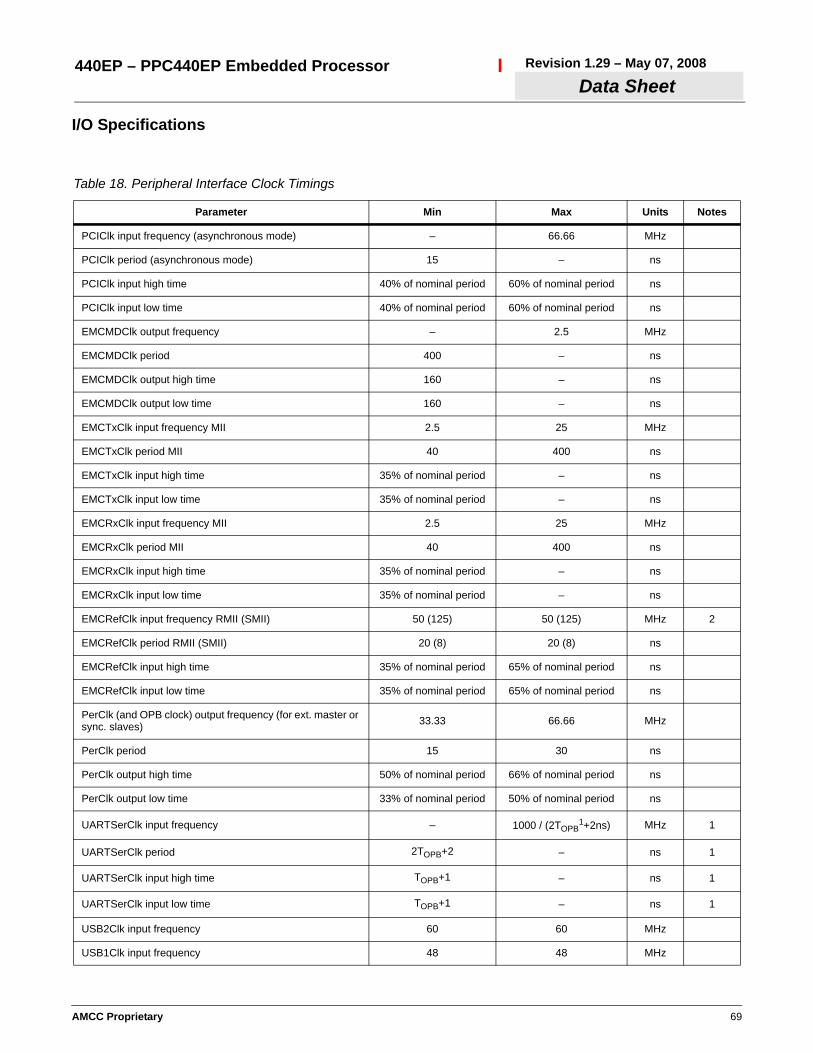
AMCC Proprietary 69
440EP – PPC440EP Embedded ProcessorData Sheet
Revision 1.29 – May 07, 2008
I/O Specifications
Table 18. Peripheral Interface Clock Timings
Parameter Min Max Units Notes
PCIClk input frequency (asynchronous mode) – 66.66 MHz
PCIClk period (asynchronous mode) 15 – ns
PCIClk input high time 40% of nominal period 60% of nominal period ns
PCIClk input low time 40% of nominal period 60% of nominal period ns
EMCMDClk output frequency – 2.5 MHz
EMCMDClk period 400 – ns
EMCMDClk output high time 160 – ns
EMCMDClk output low time 160 – ns
EMCTxClk input frequency MII 2.5 25 MHz
EMCTxClk period MII 40 400 ns
EMCTxClk input high time 35% of nominal period – ns
EMCTxClk input low time 35% of nominal period – ns
EMCRxClk input frequency MII 2.5 25 MHz
EMCRxClk period MII 40 400 ns
EMCRxClk input high time 35% of nominal period – ns
EMCRxClk input low time 35% of nominal period – ns
EMCRefClk input frequency RMII (SMII) 50 (125) 50 (125) MHz 2
EMCRefClk period RMII (SMII) 20 (8) 20 (8) ns
EMCRefClk input high time 35% of nominal period 65% of nominal period ns
EMCRefClk input low time 35% of nominal period 65% of nominal period ns
PerClk (and OPB clock) output frequency (for ext. master or sync. slaves) 33.33 66.66 MHz
PerClk period 15 30 ns
PerClk output high time 50% of nominal period 66% of nominal period ns
PerClk output low time 33% of nominal period 50% of nominal period ns
UARTSerClk input frequency – 1000 / (2TOPB1+2ns) MHz 1
UARTSerClk period 2TOPB+2 – ns 1
UARTSerClk input high time TOPB+1 – ns 1
UARTSerClk input low time TOPB+1 – ns 1
USB2Clk input frequency 60 60 MHz
USB1Clk input frequency 48 48 MHz

70 AMCC Proprietary
440EP – PPC440EP Embedded ProcessorRevision 1.29 – May 07, 2008Data Sheet
Figure 6. Input Setup and Hold Waveform
Figure 7. Output Delay and Float Timing Waveform
TmrClk input frequency – 100 MHz
TmrClk period 10 – ns
TmrClk input high time 40% of nominal period 60% of nominal period ns
TmrClk input low time 40% of nominal period 60% of nominal period ns
Notes:1. TOPB is the period in ns of the OPB clock. The internal OPB clock runs at 1/2 the frequency of the PLB clock. The maxi-
mum OPB clock frequency is 66.66 MHz.2. In RMII mode, a 50MHz +/- 50PPM input EMCRefClk is required. In SMII mode, a 125 MHz +/- 100PPM input EMCRefClk
is required.
Table 18. Peripheral Interface Clock Timings (Continued)
Parameter Min Max Units Notes
Clock
TIS TIHmin min
Inputs
Valid
1.25V
Valid
Clock
Outputs
Valid
TOH min
TOVmaxTOVmax
TOH min
TOVmax
TOH min
Float (High-Z)
High (Drive)
Low (Drive)
1.25V

AMCC Proprietary 71
440EP – PPC440EP Embedded ProcessorData Sheet
Revision 1.29 – May 07, 2008
Table 19. I/O Specifications—PCI, USB, UART, IIC, SPI, Ethernet, System and Debug Interfaces (Sheet 1 of 3)Notes:1. Ethernet interface meets timing requirements as defined by IEEE 802.3 standard.2. EMCSync is a weak driver. Redrive EMCSync when driving more than one load.
SignalInput (ns) Output (ns) Output Current (mA)
Clock NotesSetup Time(TIS min)
Hold Time(TIH min)
Valid Delay(TOV max)
Hold Time(TOH min)
I/O H(minimum)
I/O L(minimum)
PCI InterfacePCIAD31:00 5 0 6 2 0.5 1.5 PCIClkPCIC3:0/BE3:0 5 0 6 2 0.5 1.5 PCIClkPCIDevSel 5 0 6 2 0.5 1.5 PCIClkPCIFrame 5 0 6 2 0.5 1.5 PCIClkPCIGnt0:5 6 2 0.5 1.5 PCIClkPCIIDSel 5 0 n/a n/a PCIClkPCIINT 6 2 0.5 1.5 PCIClk asyncPCIIRDY 5 0 6 2 0.5 1.5 PCIClkPCIPar 5 0 6 2 0.5 1.5 PCIClkPCIPErr 5 0 6 2 0.5 1.5 PCIClkPCIReq0:5 5 0 n/a n/a PCIClkPCIReset n/a n/a PCIClkPCISErr 5 0 6 2 0.5 1.5 PCIClkPCIStop 5 0 6 2 0.5 1.5 PCIClkPCITRDY 5 0 6 2 0.5 1.5 PCIClkEthernet MII InterfaceEMCCD 10 10 5.1 6.8 1, asyncEMCCrS 10 10 5.1 6.8 1, asyncEMCDV 10 10 5.1 6.8EMCMDClk 5.1 6.8 1, asyncEMCMDIO 5.1 6.8 EMCMDClk 1EMCRxClk 5.1 6.8 1, asyncEMCRxD0:3 10 10 5.1 6.8 EMCRxClk 1EMCRxErr 10 10 5.1 6.8 EMCRxClk 1EMCTxClk n/a n/a 1, asyncEMCTxD0:3 20 0 5.1 6.8 EMCTxClk 1EMCTxEn 20 0 5.1 6.8 EMCTxClk 1EMCTxErr 20 0 5.1 6.8 EMCTxClk 1
RejectPkt 3 1 EMCRxClkfor MII, RMII, SMII
Ethernet RMII InterfaceEMC0CRSDV 4 2EMC0RxD0:1 4 2 5.1 6.8 EMCRefClk 1EMC0RxErr 4 2 5.1 6.8 EMCRefClk 1EMC0TxD0:1 12.5 0 5.1 6.8 EMCRefClk 1EMC1CRSDV 4 2EMC1RxD0:1 4 2 5.1 6.8 EMCRefClk 1EMC1RxErr 4 2 5.1 6.8 EMCRefClk 1EMC1TxD0:1 12.5 0 5.1 6.8 EMCRefClk 1
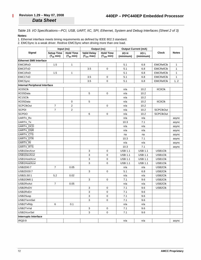
72 AMCC Proprietary
440EP – PPC440EP Embedded ProcessorRevision 1.29 – May 07, 2008Data Sheet
Ethernet SMII InterfaceEMC0RxD 1.5 1 5.1 6.8 EMCRefClk 1EMC0TxD 3.5 0 5.1 6.8 EMCRefClk 1EMC1RxD 1.5 1 5.1 6.8 EMCRefClk 1EMC1TxD 3.5 0 5.1 6.8 EMCRefClk 1EMCSync 3.5 0 5.1 6.8 EMCRefClk 1, 2Internal Peripheral InterfaceIIC0SClk n/a 10.2 IIC0ClkIIC0SData 5 0 n/a 10.2IIC1SClk n/a 10.2IIC0SData 0 5 n/a 10.2 IIC0ClkSCPClkOut 7 2 0 n/a 10.2SCPDI 7 2 n/a 10.2 SCPClkOutSCPDO 6 0 n/a 10.2 SCPClkOutUARTn_Rx n/a n/a asyncUARTn_Tx 10.3 7.1 asyncUARTn_DCD n/a n/a asyncUARTn_DSR n/a n/a asyncUARTn_CTS na na asyncUARTn_DTR 10.3 7.1 asyncUARTn_RI n/a n/a asyncUARTn_RTS 10.3 7.1 asyncUSB1DevXcvr 3 0 USB 1.1 USB 1.1 USB1ClkUSB1DevXcvr 3 0 USB 1.1 USB 1.1 USB1ClkUSB1HostXcvr 3 0 USB 1.1 USB 1.1 USB1ClkUSB1HostXcvr 3 0 USB 1.1 USB 1.1 USB1ClkUSB2DI0:7 7 0.05 n/a n/a USB2ClkUSB2DO0:7 3 0 5.1 6.8 USB2ClkUSB2LS0:1 5.2 0.02 n/a n/a USB2ClkUSB2OM0:1 3 0 7.1 9.6 USB2ClkUSB2RxAct 7 0.05 n/a n/a USB2ClkUSB2RxDV 3 0 7.1 9.6 USB2ClkUSB2RxErr 3 0 7.1 9.6USB2Susp 3 0 7.1 9.6USB2TermSel 3 0 7.1 9.6USB2TxRdy 6 0.1 n/a n/aUSB2TxVal 3 0 7.1 9.6USB2XcvrSel 3 0 7.1 9.6Interrupts InterfaceIRQ0:9 n/a n/a async
Table 19. I/O Specifications—PCI, USB, UART, IIC, SPI, Ethernet, System and Debug Interfaces (Sheet 2 of 3)Notes:1. Ethernet interface meets timing requirements as defined by IEEE 802.3 standard.2. EMCSync is a weak driver. Redrive EMCSync when driving more than one load.
SignalInput (ns) Output (ns) Output Current (mA)
Clock NotesSetup Time(TIS min)
Hold Time(TIH min)
Valid Delay(TOV max)
Hold Time(TOH min)
I/O H(minimum)
I/O L(minimum)

AMCC Proprietary 73
440EP – PPC440EP Embedded ProcessorData Sheet
Revision 1.29 – May 07, 2008
JTAG InterfaceTCK n/a n/a asyncTDI n/a n/a asyncTDO 15.3 10.2 asyncTMS n/a n/a asyncTRST n/a n/a asyncSystem InterfaceSysReset n/a n/a asyncHalt n/a n/a asyncSysErr 10.3 7.1 asyncGPIO00:63 10.3 7.1Trace InterfaceTrcClk 10.3 7.1TrcBS0:2 10.3 7.1 TrcBS0:2TrcES0:4 10.3 7.1 TrcES0:4TrcTS0:6 10.3 7.1 TrcTS0:6
Table 19. I/O Specifications—PCI, USB, UART, IIC, SPI, Ethernet, System and Debug Interfaces (Sheet 3 of 3)Notes:1. Ethernet interface meets timing requirements as defined by IEEE 802.3 standard.2. EMCSync is a weak driver. Redrive EMCSync when driving more than one load.
SignalInput (ns) Output (ns) Output Current (mA)
Clock NotesSetup Time(TIS min)
Hold Time(TIH min)
Valid Delay(TOV max)
Hold Time(TOH min)
I/O H(minimum)
I/O L(minimum)
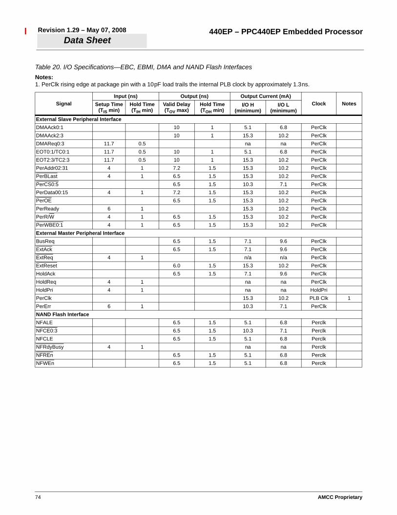
74 AMCC Proprietary
440EP – PPC440EP Embedded ProcessorRevision 1.29 – May 07, 2008Data Sheet
Table 20. I/O Specifications—EBC, EBMI, DMA and NAND Flash InterfacesNotes:1. PerClk rising edge at package pin with a 10pF load trails the internal PLB clock by approximately 1.3ns.
SignalInput (ns) Output (ns) Output Current (mA)
Clock NotesSetup Time(TIS min)
Hold Time(TIH min)
Valid Delay(TOV max)
Hold Time(TOH min)
I/O H(minimum)
I/O L(minimum)
External Slave Peripheral InterfaceDMAAck0:1 10 1 5.1 6.8 PerClkDMAAck2:3 10 1 15.3 10.2 PerClkDMAReq0:3 11.7 0.5 na na PerClkEOT0:1/TC0:1 11.7 0.5 10 1 5.1 6.8 PerClkEOT2:3/TC2:3 11.7 0.5 10 1 15.3 10.2 PerClkPerAddr02:31 4 1 7.2 1.5 15.3 10.2 PerClkPerBLast 4 1 6.5 1.5 15.3 10.2 PerClkPerCS0:5 6.5 1.5 10.3 7.1 PerClkPerData00:15 4 1 7.2 1.5 15.3 10.2 PerClkPerOE 6.5 1.5 15.3 10.2 PerClkPerReady 6 1 15.3 10.2 PerClkPerR/W 4 1 6.5 1.5 15.3 10.2 PerClkPerWBE0:1 4 1 6.5 1.5 15.3 10.2 PerClkExternal Master Peripheral InterfaceBusReq 6.5 1.5 7.1 9.6 PerClkExtAck 6.5 1.5 7.1 9.6 PerClkExtReq 4 1 n/a n/a PerClkExtReset 6.0 1.5 15.3 10.2 PerClkHoldAck 6.5 1.5 7.1 9.6 PerClkHoldReq 4 1 na na PerClkHoldPri 4 1 na na HoldPriPerClk 15.3 10.2 PLB Clk 1PerErr 6 1 10.3 7.1 PerClkNAND Flash InterfaceNFALE 6.5 1.5 5.1 6.8 PerclkNFCE0:3 6.5 1.5 10.3 7.1 PerclkNFCLE 6.5 1.5 5.1 6.8 PerclkNFRdyBusy 4 1 na na PerclkNFREn 6.5 1.5 5.1 6.8 PerclkNFWEn 6.5 1.5 5.1 6.8 Perclk

AMCC Proprietary 75
440EP – PPC440EP Embedded ProcessorData Sheet
Revision 1.29 – May 07, 2008
DDR1 SDRAM I/O Specifications
The DDR1 SDRAM controller times its operation with internal PLB clock signals and generates MemClkOut0 from the PLB clock. The PLB clock is an internal signal that cannot be directly observed. However MemClkOut0 is the same frequency as the PLB clock signal and is in phase with the PLB clock signal.
Note: MemClkOut0 can be advanced with respect to the PLB clock by means of the SDRAM0_CLKTR programming register. In a typical system, users advance MemClkOut by 90°. This depends on the specific application and requires a thorough understanding of the memory system in general (refer to the DDR SDRAM controller chapter in the PowerPC 440EP User’s Manual).
In the following sections, the label MemClkOut0(0) refers to MemClkOut0 when it has not been phase-shifted, and MemClkOut0(90) refers to MemClkOut0 when it has been phase-advanced 90°. Advancing MemClkOut0 by 90° creates a 3/4 cycle setup time and 1/4 cycle hold time for the address and control signals in relation to MemClkOut0(90). The rising edge of MemClkOut0(90) aligns with the first rising edge of the DQS signal.
The following DDR data is generated by means of simulation and includes logic, driver, package RLC, and lengths. Values are calculated over best case and worst case processes with speed, temperature, and voltage as follows:
Best Case = Fast process, -40°C, +1.6V
Worst Case = Slow process, +85°C, +1.4V
Note: In all the following DDR tables and timing diagrams, minimum values are measured under best case conditions and maximum values are measured under worst case conditions.
The signals are terminated as indicated in the figure below for the DDR timing data in the following sections.
Figure 8. DDR SDRAM Simulation Signal Termination Model
10pF
10pF
MemClkOut0
MemClkOut0
120Ω
50Ω
30pF
Addr/Ctrl/Data/DQS
VTT = SVDD/2PPC440EP
Note: This diagram illustrates the model of the DDR SDRAM interface used when generating simulation timing data.It is not a recommended physical circuit design for this interface. An actual interface design will depend on manyfactors, including the type of memory used and the board layout.

76 AMCC Proprietary
440EP – PPC440EP Embedded ProcessorRevision 1.29 – May 07, 2008Data Sheet
Table 21. DDR SDRAM Output Driver Specifications
Signal PathOutput Current (mA)
I/O H (maximum) I/O L (minimum)Write DataMemData00:07 15.2 15.2MemData08:15 15.2 15.2MemData16:23 15.2 15.2MemData24:31 15.2 15.2ECC0:7 15.2 15.2DM0:8 15.2 15.2MemClkOut0 15.2 15.2MemAddr00:12 15.2 15.2BA0:1 15.2 15.2RAS 15.2 15.2CAS 15.2 15.2WE 15.2 15.2BankSel0:3 15.2 15.2ClkEn0:3 15.2 15.2DQS0:8 15.2 15.2
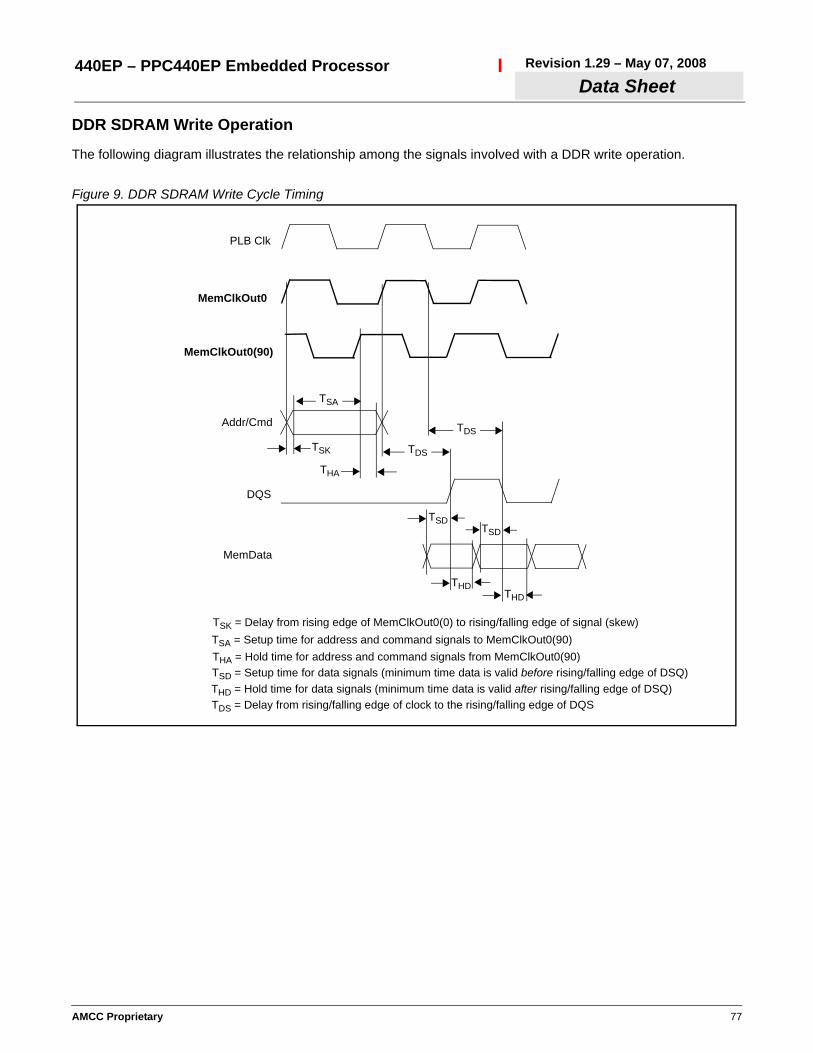
AMCC Proprietary 77
440EP – PPC440EP Embedded ProcessorData Sheet
Revision 1.29 – May 07, 2008
DDR SDRAM Write Operation
The following diagram illustrates the relationship among the signals involved with a DDR write operation.
Figure 9. DDR SDRAM Write Cycle Timing
DQS
MemData
PLB Clk
MemClkOut0
MemClkOut0(90)
Addr/Cmd
TSK
TSA
THA
TDS
TDS
TSD
THD
TSD
THD
TSA = Setup time for address and command signals to MemClkOut0(90)TSK = Delay from rising edge of MemClkOut0(0) to rising/falling edge of signal (skew)
THA = Hold time for address and command signals from MemClkOut0(90)
TDS = Delay from rising/falling edge of clock to the rising/falling edge of DQS
TSD = Setup time for data signals (minimum time data is valid before rising/falling edge of DSQ)THD = Hold time for data signals (minimum time data is valid after rising/falling edge of DSQ)

78 AMCC Proprietary
440EP – PPC440EP Embedded ProcessorRevision 1.29 – May 07, 2008Data Sheet
Note: The timing data in the following tables is based on simulation runs using Einstimer.
Table 22. I/O Timing—DDR SDRAM TDS
Notes:1. All of the DQS signals are referenced to MemClkOut0(0).2. Clock speed is 133MHz.3. The TDS values in the table include 3/4 of a cycle at 133MHz (7.5ns x 0.75 = 5.625 ns).4. To obtain adjusted values for lower clock frequencies, subtract 5.625 ns from the values in the table and add 3/4 of the cycle
time for the lower clock frequency (TDS - 5.625 + 0.75TCYC).
Signal NameTDS (ns)
Minimum MaximumDQS0 5.76 5.86DQS1 5.78 5.91DQS2 5.82 5.90DQS3 5.79 5.89DQS8 5.75 5.88
Table 23. I/O Timing—DDR SDRAM TSK, TSA, and THA
Notes:1. Clock speed is 133MHz. TSK is referenced to MemClkOut0(0). TSA and THA are referenced to MemClkOut0(90).2. To obtain adjusted TSA values for lower clock frequencies, use 3/4 of the cycle time for the lower clock frequency and subtract
TSK maximum (0.75TCYC - TSKmax).3. To obtain adjusted THA values for lower clock frequencies, use 1/4 of the cycle time for the lower clock frequency and add
TSK minimum (0.25TCYC + TSKmin).
Signal NameTSK (ns) TSA (ns) THA (ns)
Minimum Maximum Minimum MinimumMemAddr00:12 0.11 0.32 5.31 1.99BA0:1 0.07 0.31 5.32 1.95BankSel0:3 0.05 0.25 5.38 1.93ClkEn0:3 0.07 0.28 5.35 1.95CAS 0.05 0.31 5.32 1.93RAS 0.05 0.28 5.35 1.93WE 0.08 0.22 5.41 1.96
Table 24. I/O Timing—DDR SDRAM TSD and THD
Notes:1. TSD and THD are measured under worst case conditions.2. Clock speed for the values in the table is 133MHz.3. The time values in the table include 1/4 of a cycle at 133MHz (7.5ns x 0.25 = 1.875 ns).4. To obtain adjusted TSD and THD values for lower clock frequencies, subtract 1.875 ns from the values in the table and add
1/4 of the cycle time for the lower clock frequency (e.g., TSD - 1.875 + 0.25TCYC).
Signal Names Reference Signal TSD (ns) THD (ns)
MemData00:07, DM0 DQS0 1.795 1.866MemData08:15, DM1 DQS1 1.775 1.865MemData16:23, DM2 DQS2 1.745 1.862MemData24:31, DM3 DQS3 1.765 1.864ECC0:7, DM8 DQS8 1.685 1.857

AMCC Proprietary 79
440EP – PPC440EP Embedded ProcessorData Sheet
Revision 1.29 – May 07, 2008
DDR SDRAM Read Operation
The following examples of timing for DDR SDRAM read operations are based on the relationship between the incoming data and the PLB clock signal. Since the PLB clock cannot be directly observed, the delay of MemClkOut(0) relative to the PLB clock (TMD) is provided.
The internal Read Clock signal, like MemClkOut0, is derived from the PLB clock and can be delayed relative to the PLB clock by programming the RDCT and RDCD fields in the SDRAM0_TR1 register. The delay can be programmed from 0 to 1/2 cycle in steps using RDCT. Setting RDCD results in a 1/2 cycle delay plus the value set in RDCT. The delay of Read Clock relative to the PLB clock (TRD) shown below assumes the programmable Read Clock delay is set to zero.
Figure 10. DDR SDRAM MemClkOut0 and Read Clock Delay
In operation, following the receipt of an address and read command from the PPC440EP, the SDRAM generates data and the DQS signals coincident with MemClkOut0. The data is latched into the PPC440EP using a DQS signal that is delayed 1/4 of a cycle. In order to accommodate timing variations introduced by the system designs using this chip, the three-stage data path shown below is used to eliminate metastability and allow data sampling to be adjusted for minimum latency. This adjustment requires programming the Read Clock delay and the selection of Stage 1, Stage 2, or Stage 3 data for sampling at Read Sample Point flipflop (RDSP).
Read Clock
PLB Clk
MemClkOut0(0)
TMD
TRD
TMDmin = 600psTMDmax = 1100ps
TRDmin = 300psTRDmax = 740ps
min values assume best case conditions.max values assume worst case conditions.
Note:
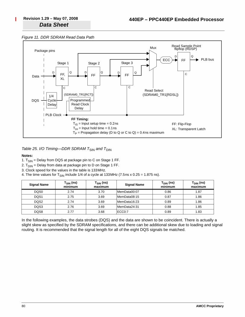
80 AMCC Proprietary
440EP – PPC440EP Embedded ProcessorRevision 1.29 – May 07, 2008Data Sheet
Figure 11. DDR SDRAM Read Data Path
In the following examples, the data strobes (DQS) and the data are shown to be coincident. There is actually a slight skew as specified by the SDRAM specifications, and there can be additional skew due to loading and signal routing. It is recommended that the signal length for all of the eight DQS signals be matched.
Table 25. I/O Timing—DDR SDRAM TSIN and TDIN
Notes:1. TSIN = Delay from DQS at package pin to C on Stage 1 FF.2. TDIN = Delay from data at package pin to D on Stage 1 FF.3. Clock speed for the values in the table is 133MHz.4. The time values for TSIN include 1/4 of a cycle at 133MHz (7.5ns x 0.25 = 1.875 ns).
Signal Name TSIN (ns)minimum
TSIN (ns)maximum Signal Name TDIN (ns)
minimumTDIN (ns)
maximumDQS0 2.74 3.70 MemData00:07 0.86 1.87DQS1 2.75 3.69 MemData08:15 0.87 1.86DQS2 2.74 3.69 MemData16:23 0.89 1.86DQS3 2.76 3.69 MemData24:31 0.88 1.85DQS8 2.77 3.68 ECC0:7 0.89 1.83
(SDRAM0_TR1[RCT])
Stage 1 Stage 2 Stage 3
Read Sample Point
PLB bus
FF, FF FF
FF
Data
Read Select(SDRAM0_TR1[RDSL])
DQS1/4
CycleDelay
PLB Clock
Programmed
Delay
D
C
Package pinsMux
Read Clock
C C
CD D
D
FF Timing:TIS = Input setup time = 0.2nsTIH = Input hold time = 0.1nsTP = Propagation delay (D to Q or C to Q) = 0.4ns maximum
XL
ECC
FF: Flip-FlopXL: Transparent Latch
Q Q Q
Q
flipflop (RDSP)

AMCC Proprietary 81
440EP – PPC440EP Embedded ProcessorData Sheet
Revision 1.29 – May 07, 2008
Example 1:If the data-to-PLB clock timing is as shown in the example below, then the read clock is not delayed and the Stage 1 data is sampled at (1). Except for small, low frequency memory systems with the memory located physically close to the PPC440EP, it is unlikely that Stage 1 data can be sampled. When the data comes later, it is necessary to sample Stage 2 or Stage 3 data. (see Examples 2 and 3). Another way to get the desired data-to-PLB timing to allow Stage 1 sampling is to buffer MemClkOut0 and skew it enough to guarantee the timing. In this example, TT is system dependent and taken into account by controller initialization software.
Figure 12. DDR SDRAM Read Cycle Timing—Example 1
DQS at pin
PLB Clock
TSIN
TDIN = Delay from data at package pin to D on Stage 1 FF.
TSIN = Delay from DQS at package pin to C on Stage 1 FF.
Data at pin D0 D1 D2 D3
DQS Stage 1 C
D0 D1 D2 D3TDIN
D0 D2
Data in Stage 1 D
D1 D3
Data out Stage 1High
Low
TP
D0 D2
D1 D3
Data in at RDSP High
Lowwith no ECC
TT
TP = Propagation delay through FFs
TT = Propagation delay, Stage 1 input to RDSP input w/o ECC
D0 D2
D1 D3Data out RDSP
High
Low
(1)
D2
D2
TP
D0
D0

82 AMCC Proprietary
440EP – PPC440EP Embedded ProcessorRevision 1.29 – May 07, 2008Data Sheet
Example 2:In this example Read Clock is delayed almost 1/2 cycle. Without ECC, Stage 2 data can be sampled at (2). If ECC is enabled, Stage 3 data must be sampled (see Example 3). In this example, TT and TTE are system dependent and taken into account by controller initialization software.
Figure 13. DDR SDRAM Read Cycle Timing—Example 2
DQS at pin
PLB Clock
Read Clock Delayed
TSIN
Data at pin D0 D1 D2 D3
DQS Stage 1 C
D0 D1 D2 D3TDIN
D0 D2
Data in Stage 1 D
D1 D3
Data out Stage 1High
Low
TP
D0 D2
D1 D3
Data in at RDSP High
Lowwithout ECC
TT = Propagation delay from Stage 2 input to RDSP input w/o ECC
D0 D2
D1 D3Data out Stage 2
High
Low
Data out at RDSPHigh
Low
(2)
without ECC
TP
D0 D2
D1 D3
Data in at RDSP High
Lowwith ECC
D0 D2
D1 D3
TTE = Propagation delay from Stage 2 input to RDSP input with ECC
TTTTE
D0 D2

AMCC Proprietary 83
440EP – PPC440EP Embedded ProcessorData Sheet
Revision 1.29 – May 07, 2008
Example 3:In this example, ECC is enabled. This requires that Stage 3 data be sampled at (3). If ECC is disabled, the system will still work, but there will be more latency before the data is sampled into RDSP. In this example, TT and TTE are system dependent and taken into account by controller initialization software.
Figure 14. DDR SDRAM Read Cycle Timing—Example 3
DQS at pin
PLB Clock
Read Clock Delayed
TSIN
Data at pin D0 D1 D2 D3
DQS Stage 1 C
D0 D1 D2 D3TDIN
D0 D2
Data in Stage 1 D
D1 D3
Data out Stage 1High
Low
TP
D0 D2
D1 D3
Data out Stage 3 High
Lowwith ECC
TT = Propagation delay from Stage 2 input to RDSP input w/o ECC
D0 D2
D1 D3Data out Stage 2
High
Low
Data out RDSPHigh
Low
(3)
with ECC
TP
D0 D2
D1 D3
Data in at RDSP High
Lowwith ECC
D0 D2
D1 D3
TTE = Propagation delay from Stage 2 input to RDSP input with ECC
TTE
D0 D2

84 AMCC Proprietary
440EP – PPC440EP Embedded ProcessorRevision 1.29 – May 07, 2008Data Sheet
Initialization
The PPC440EP provides the option for setting initial parameters based on default values or by reading them from a slave PROM attached to the IIC0 bus (see “EEPROM” below). Some of the default values can be altered by strapping on external pins (see “Strapping” below).
Strapping
While the SysReset input pin is low (system reset), the state of certain I/O pins is read to enable certain default initial conditions prior to PPC440EP start-up. The actual capture instant is the nearest reference clock edge before the deassertion of reset. These pins must be strapped using external pull-up (logical 1) or pull-down (logical 0) resistors to select the desired default conditions. These pins are used for strap functions only during reset. Following reset they are used for normal functions. The signal names assigned to the pins for normal operation are shown in parentheses following the pin number.
To isolate the strapping pins, the ExtReset signal may be used as a buffer enable or multiplexer select.
The following table lists the strapping pins along with their functions and strapping options:
EEPROM
During reset, initial conditions other than those obtained from the strapping pins can be read from a ROM device connected to the IIC0 port. At the de-assertion of reset, if the bootstrap controller is enabled, the PPC440EP sequentially reads 16 bytes from the ROM device on the IIC0 port and sets the SDR0_SDSTP0, SDR0_SDSTP1, SDR0_SDSTP2 and SDR0_SDSTP3 registers accordingly.
The initialization settings and their default values are covered in detail in the PowerPC 440EP User’s Manual.
Table 26. Strapping Pin Assignments
Function OptionBall Strapping
R25(UART0_DCD)
U26(UART0_DSR)
V26(UART0_CTS)
Serial device is disabled. Each of the six options (A–F) is a combination of boot source, boot-source width, and clock frequency specifications. Refer to the IIC Bootstrap Controller chapter in the PPC440EP Embedded Processor User’s Manual for details.
A 0 0 0
B 0 0 1
C 0 1 0
D 0 1 1
E 1 0 0
F 1 1 0
Serial device is enabled. The option being selected is the IIC0 slave address that will respond with configuration data.Note: If reading of configuration data from the serial device fails, the PPC440EP defaults to configuration X.
G (0xA8) 1 0 1
H (0xA4) 1 1 1
AMCC Proprietary 85
440EP – PPC440EP Embedded ProcessorData Sheet
Revision 1.29 – May 07, 2008
Revision Log
Date Version Contents of Modification
08/21/2003 Initial creation of document.
09/22/2003 Misc. updates and corrections.
10/07/2003 Misc. updates and corrections.
10/13/2003 Add I/O timing.
10/31/2003 Miscellaneous updates.
11/03/2003 Correct initialization strapping pins and response IIC interface.
11/25/2003 Correct OVDD and SVDD pin assignments.
12/15/2003 Delete heat sink mounting information placeholders and remove Confidential status.
12/19/2003 Restore Confidential status.
01/12/2004 Update DDR SDRAM interface timing section.
03/15/2004
Correct MemClkOut0 pin assignment.Correct SDRAM PLL voltage.Add Note 6 to UARTn_CTS signal.Correct SDRAM I/O worst case spec temperature.Change 333MHz to 400MHz.
04/7/2004 Correct label on Ethernet transmit signals.
09/2/2004 Convert to AMCC format.
09/8/2004Modify headers to flip between left and right pages like the footers.Change part numbers to AMCC part numbers.Remove Confidential status, again
09/28/2004Add USB clock frequency numbers.Number table and figure captions.
10/06/2004Correct USB block diagram and description.Update formatting and PDF book marking.
10/12/2004 Add missing DDR SDRAM timing data.
10/28/2004 Miscellaneous updates.
11/18/2004
Add RejectPkt signal to pin Y25. Issue 31Corrected numbering on PCIReq signal. Issue 30Added notes to USB signals to correctly define required pull-ups and pull-downs. Issue 20Correct typo on voltage specification for SAVDD in the DC Power Supply Loads table. Issue 9
Misc. typo corrections. Issue 29
11/19/2004 Change bootstrap option numbers to letters and add two options.
11/22/2004 Correct bootstrap pin settings to match new letter designations.
12/17/2004 Add Revision B part numbers for both leaded and lead-free packages and tape-and-reel shipping.
01/18/2005Add input capacitance values.Update and add missing voltage supply currents.
01/31/2005 Update DDR SDRAM timing.
02/08/2005 Change circuit type info for some system interface signals and move RejectPkt to the Ethernet group.

86 AMCC Proprietary
440EP – PPC440EP Embedded ProcessorRevision 1.29 – May 07, 2008Data Sheet
02/15/2005 Miscellaneous updates
03/10/2005 Miscellaneous updates
03/25/2005 Correct I/O timing specs for ExtReq signal.
04/27/2005 USB 2.0 I/O and DDR SDRAM timing updates.
05/24/2005 Add RoHS compliance statement.
06/14/2005Updates and additions to power and thermal specifications.Add new 667MHz PNs and remove old 466MHz PNs.
07/06/2005 Change maximum NAND Flash to 256MB.
08/08/2005 Change solder ball size specification and add thermally enhanced package specification.
10/05/2005 1.20 Miscellaneous updates
11/18/2005 1.21
Remove metal-layer specification from technology description.Change default configuration when bootstrap IIC read fails from option A to configuration X.Add package nomenclature.Correct MemClkOut duty cycle.Correct and move PerErr signal description from master to slave.Change maximum VCO frequency to 1334MHz.
02/16/2006 1.22 Add revision level 2.1 (C) part number and PVR number.
05/24/2006 1.23 Update power dissipation and add additional temperature data.
07/19/2006 1.24 Correct enable/disable specifications for PCI Gnt/Req signals.
12/18/2006 1.25
Change analog voltage filter circuit inductor part number.Change all multiplexed GPIO signal defaults to the GPIO signals.Change AC12 default from IRQ5 to DMAReq1.Correct descriptions of LeakTest, RcvrInh, ModeCtrl, RefEn, and DrvrInh1:2 signalsRemove “Preliminary” status from header.
04/25/2007 1.26 Remove thermally enhanced package.
01/07/2008 1.27
Added Assembly Requirements section on page 17, added Unused I/Os section on page 50, place the analog filter diagram in its own section.Added changes to the Internal Buses, changes to Assembly Requirements, moved diagram from under Device Characteristics to Power Sequencing and added more information, added information to DDR SDRAM Read Data Path Diagram, added information to Test Condition and I/O Specifications diagrams.Changed the techncial support telephone and fax number.Changed temperature rating for 333MHz and 400MHz parts on page 4 as per Product Change Notification: 091207-01.Added note for EMCSync signal to I/O Specification table.Added timing references to I/O Specification tables.Corrected setup and hold timing for RejectPK in I/O Specification table.Added definition for RDSP abbreviation to DDR SDRAM Read Data Path figure.Added notes 3 and 4 to Recommended DC Operating Conditions table.Added Overshoot/Undershoot specification.Removed references to PPC440EP Rev B part number since these parts are no longer available for ordering.
03/18/2008 1.28Replaced 16750 compatible UART to 16550Replaced NS16750 with NS16550.
05/07/2008 1.29 Deleted incorrect MDIO timing data from table 19.
Date Version Contents of Modification

AMCC Proprietary 87
440EP – PPC440EP Embedded ProcessorData Sheet
Revision 1.29 – May 07, 2008
Applied Micro Circuits Corporation215 Moffett Park Drive, Sunnyvale, CA 94089Phone: (408) 542-8600 — Fax: (408) 542-8601
http://www.amcc.com
AMCC reserves the right to make changes to its products, its data sheets, or related documentation, without notice and war-rants its products solely pursuant to its terms and conditions of sale, only to substantially comply with the latest available datasheet. Please consult AMCC’s Term and Conditions of Sale for its warranties and other terms, conditions and limitations.AMCC may discontinue any semiconductor product or service without notice, and advises its customers to obtain the latestversion of relevant information to verify, before placing orders, that the information is current. AMCC does not assume any lia-bility arising out of the application or use of any product or circuit described herein, neither does it convey any license underits patent rights nor the rights of others. AMCC reserves the right to ship devices of higher grade in place of those of lowergrade. AMCC SEMICONDUCTOR PRODUCTS ARE NOT DESIGNED, INTENDED, AUTHORIZED, OR WARRANTED TO BESUITABLE FOR USE IN LIFE-SUPPORT APPLICATIONS, DEVICES OR SYSTEMS OR OTHER CRITICALAPPLICATIONS. AMCC is a registered Trademark of Applied Micro Circuits Corporation. Copyright © 2007 Applied Micro Circuits Corporation.All Rights Reserved.