Embed Size (px)
Citation preview
MR. S. HABIB HUSSAIN, AP/CSE, MAHALAKSHMI ENGINEERING COLLEGE, TRICHY – 621 213Page 1
Dept.: CSE Sem: IV
Sub. Code: CS2253 Sub. Name: C.O.A
Unit – II
BASIC PROCESSING UNIT
PART – A (2 MARKS)
1. What are the relative merits of horizontal and vertical micro instruction format?
[APR/MAY 2010]
Vertical approach is the significant factor, it is used to reduce the requirement for the
parallel hardware required to handle the execution of microinstructions.
Fewer bits are required in the microinstruction.
The horizontal organization approach is suitable when operating speed of computer is
a critical factor and where the machine structure allows parallel usage of a number of
resources.
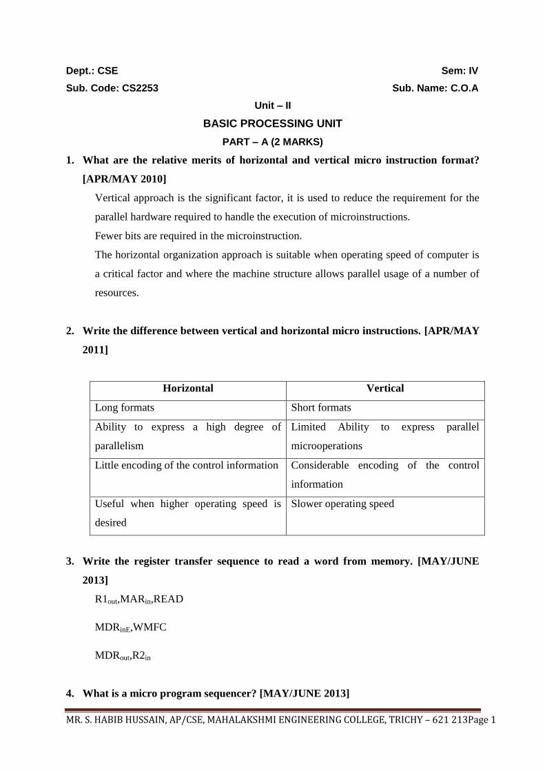
2. Write the difference between vertical and horizontal micro instructions. [APR/MAY
2011]
Horizontal Vertical
Long formats Short formats
Ability to express a high degree of
parallelism
Limited Ability to express parallel
microoperations
Little encoding of the control information Considerable encoding of the control
information
Useful when higher operating speed is
desired
Slower operating speed
3. Write the register transfer sequence to read a word from memory. [MAY/JUNE
2013]
R1out,MARin,READ
MDRinE,WMFC
MDRout,R2in
4. What is a micro program sequencer? [MAY/JUNE 2013]

MR. S. HABIB HUSSAIN, AP/CSE, MAHALAKSHMI ENGINEERING COLLEGE, TRICHY – 621 213Page 2
It is a next address generator. It determines the address sequence that is read from
control memory and next address of the next microinstruction can be specified several
way depending on the sequencer input.
5. What are the two possible error conditions that may arise in a stack operation?
[NOV/DEC 2010]
Overflow and underflow are the two possible error conditions that may arise in a stack
operation.
6. List the advantages of multibus organization. [NOV/DEC 2011] [NOV/DEC 2012]
In multibus organization, there are three buses(2 i/p bus & 1 o/p bus). So the number
of steps needed to execute instruction is reduced.
It provides multiple internal paths that enable several transfers to take place in parallel.
7. What are the inputs for hardwired control? [NOV/DEC 2011]
Contents of the control step counter
Contents of the instruction register
Contents of the condition code flags
External input signals such as MFC and interrupt requests.
8. List the advantages of register transfer. [NOV/DEC 2012]
Instruction execution involves a sequence of steps in which data are transferred from
one register to another. For each register, two control signals are used to place the
contents of that register on the bus or to load the data on the bus into the register.
9. Define exception. [NOV/DEC 2012]
The error that occurred in the process during run time is called exception.
10. Write the register transfer sequence for storing a word in memory. [MAY/JUNE
2012]
R1out, MARin
R2out, MDRin,WRITE
MDRoutE, WMFC
11. What is hardwired control? How is it different from micro programmed control?
[MAY/JUNE 2012]

MR. S. HABIB HUSSAIN, AP/CSE, MAHALAKSHMI ENGINEERING COLLEGE, TRICHY – 621 213Page 3
Hardwired control is a control mechanism to generate control signals by using
appropriate finite state machine (FSM). But, Micro programmed control is a control
mechanism to generate control signals by using a memory called control storage (CS),
which contains the control signals. Here the control units use fixed logic circuits to
interpret instructions and generate control signals from them.
PART-B
1. Draw and explain the block diagram of a complete processor. (6) [APR/MAY
2010]
With a neat diagram explain the internal organization of a processor. (6)
[MAY/JUNE 2012]
This diagram consists of instruction unit, integer unit, floating point unit,
instruction cache, data cache, bus interface unit, main memory module and
input/output module. The instruction unit fetches instruction from an instruction
cache or from main memory when the desired instructions are not available in the
cache.
The complete processor provides 2 processing units: integer unit and floating point
unit.
Integer unit is to process integer data and floating point unit is to process floating
point data.
These 2 units get data from data cache.
Use of separate cache for instruction and data is common in practice.
Other processors use a common single cache for both instructions and data. The
80486 processor has 8 K bytes single cache for both instruction and data whereas
the Pentium processor has separate 8 K bytes caches for instruction and data.
It provides bus interface unit to control the interface of processor to system bus,
mainmemory module and input/output

MR. S. HABIB HUSSAIN, AP/CSE, MAHALAKSHMI ENGINEERING COLLEGE, TRICHY – 621 213Page 4
module.
2. Briefly describe the design of a hardwired control unit. (10) (8) [APR/MAY
2010] [MAY/JUNE 2012]
Describe the control unit organization with a separate Encoder and Decoder
functions in a hardwired control. (8) [APR/MAY 2011]
To execute instructions, a computer's processor must generate the control
signals used to perform the processor's actions in the proper sequence. This
sequence of actions can either be executed by another processor's software or in
hardware.
Hardware signals are generated either by hardwired control, in which the
instruction bits directly generate the signals.
Hardwired control usually was implemented using discrete components, flip-
chips, or even rotating discs or drums.
Instruction
unit
Integer unit Floating
point unit
Instruction
cache
Data cache
Bus interface unit
Main memory
module
Input/output
module
System bus

MR. S. HABIB HUSSAIN, AP/CSE, MAHALAKSHMI ENGINEERING COLLEGE, TRICHY – 621 213Page 5
The control units use fixed logic circuits to interpret instructions and generate
control signals.
The control signals are generated by the following information.
Contents of the control step counter
Contents of the instruction register
Contents of the condition code flags
External input signals such as MFC and interrupt requests.
The fixed logic circuit block includes combinational circuit that generates the
required control outputs for decoding and encoding functions.
Control signals

MR. S. HABIB HUSSAIN, AP/CSE, MAHALAKSHMI ENGINEERING COLLEGE, TRICHY – 621 213Page 6
The ID decodes the instruction loaded in the IR. If IR is 8 bit register then
instruction decoder generates 28 i.e. 256 lines one for each instruction.
According to the code in the IR, only one amongst all output lines of decoder
INS 1 through INSm goes high i.e. set to 1 and all other lines set to 0.
The step decoder provides a separate signal line for each step or time slot in a
control sequence.
The encoder gets input from instruction decoder, step decoder, external input
and condition codes.
It uses all these inputs to generate the individual control signals.
After execution of each instruction end is generated which resets control step
counter and make it ready for next generation of next instruction.

MR. S. HABIB HUSSAIN, AP/CSE, MAHALAKSHMI ENGINEERING COLLEGE, TRICHY – 621 213Page 7
Zin=T1+T6.ADD+T4.BR+….
The zin signal is asserted during time slot T1 for all instructions during T6
for an ADD instruction during T4 for an unconditional branch instruction.
For end signal
End= T7.ADD + T5.BR + (T5.N + T4. N) .BRN+…
The end signal starts a new instruction fetch cycle by resetting the control
step counter to its starting value.
When the control signal called RUN is set to 1 which causes the counter to
be incremented by one at the end of every clock cycle.
When RUN is equal to 0 ten counter stops counting.
This is needed whenever the WMFC signal is issued to cause the processor
to wait for the reply from the memory.
A complete processor:
This diagram consists of instruction unit, integer unit, floating point unit,
instruction cache, data cache, bus interface unit, main memory module and
input/output module.
Branch
j
Add T4
an
chj
T6
an
chj
T1
an
chj

MR. S. HABIB HUSSAIN, AP/CSE, MAHALAKSHMI ENGINEERING COLLEGE, TRICHY – 621 213Page 8
The instruction unit fetches instruction from an instruction cache or from
main memory when the desired instructions are not available in the cache.
The complete processor provides 2 processing units: integer unit and
floating point unit.
Integer unit is to process integer data and floating point unit is to process
floating point data.
These 2 units get data from data cache.
Use of separate cache for instruction and data is common in practice.
Other processors use a common single cache for both instructions and data.
The 80486 processor has 8 K bytes single cache for both instruction and
data whereas the Pentium processor has separate 8 K bytes caches for
instruction and data.
It provides bus interface unit to control the interface of processor to system
bus,main memory module and input/output
Instruction
unit
Integer unit Floating
point unit
Instruction
cache
Data cache
Bus interface unit
Main memory
module
Input/output
module
System bus

MR. S. HABIB HUSSAIN, AP/CSE, MAHALAKSHMI ENGINEERING COLLEGE, TRICHY – 621 213Page 9
3. Explain the basic organization of a micro programmed control unit and the
generation of control signals using microprogram. (12) [APR/MAY 2010]
Draw necessary diagrams and explain the control signal generation using
micro programmed control. (16) [NOV/DEC 2011]
Explain how control signals are generated using micro programmed control.
(10) [MAY/JUNE 2012]
Explain the design of micro programmed control unit in detail. (16)
[MAY/JUNE 2013]
Explain the organization of the control unit to allow conditional branching in
the microprogram. (8) [NOV/DEC 2010]
How is a functional field microinstruction generated? Explain. (8) [NOV/DEC
2010]
Every instruction in a processor is implemented by a sequence of one or more sets of
concurrent micro operations.
Each micro operation is associated with a specific set of control lines which, when
activated, causes that micro operation to take place.
Since the number of instructions and control lines is often in the hundreds, the
complexity of hardwired control unit is very high.
Thus, it is costly and difficult to design. The hardwired control unit is relatively
inflexible because it is difficult to change the design, if one wishes to correct design
error or modify the instruction set.
Microprogramming is a method of control unit design in which the control signal memory
CM.
The control signals to be activated at any time are specified by a microinstruction, which
is fetched from CM.
A sequence of one or more micro operations designed to control specific operation, such
as addition, multiplication is called a micro program.
The micro programs for all instructions are stored in the control memory.
The address where these microinstructions are stored in CM is generated by
microprogram sequencer.

MR. S. HABIB HUSSAIN, AP/CSE, MAHALAKSHMI ENGINEERING COLLEGE, TRICHY – 621 213Page 10
The address where these microinstructions are stored in CM is generated by
microprogram sequencer/microprogram controller.
The microprogram sequencer generates the address for microinstruction according to the
instruction stored in the IR.
The microprogrammed control unit,
- control memory
- control address register
- micro instruction register
- microprogram sequencer
The components of control unit work together as follows:
The control address register holds the address of the next microinstruction to be read.
When address is available in control address register, the sequencer issues READ
command to the control memory.
After issue of READ command, the word from the addressed location is read into the
microinstruction register.
Now the content of the micro instruction register generates control signals and next
address information for the sequencer.
The sequencer loads a new address into the control address register based on the next
address information.

MR. S. HABIB HUSSAIN, AP/CSE, MAHALAKSHMI ENGINEERING COLLEGE, TRICHY – 621 213Page 11
Advantages of Microprogrammed control
It simplifies the design of control unit. Thus it is both, cheaper and less error phrone
implement.
Control functions are implemented in software rather than hardware.
The design process is orderly and systematic
More flexible, can be changed to accommodate new system specifications or to correct
the design errors quickly and cheaply.

MR. S. HABIB HUSSAIN, AP/CSE, MAHALAKSHMI ENGINEERING COLLEGE, TRICHY – 621 213Page 12
Complex function such as floating point arithmetic can be realized efficiently.
Disadvantages
A microprogrammed control unit is somewhat slower than the hardwired control unit,
because time is required to access the microinstructions from CM.
The flexibility is achieved at some extra hardware cost due to the control memory and
its access circuitry.
Microinstruction
A simple way to structure microinstructions is to assign one bit position to each control signal
required in the CPU.
Grouping of control signals
Grouping technique is used to reduce the number of bits in the microinstruction.
Gating signals: IN and OUT signals
Control signals: Read,Write, clear A, Set carry in, continue operation, end, etc.
ALU signals: Add, Sub,etc;
There are 46 signals and hence each microinstruction will have 46 bits.
It is not at all necessary to use all 46 bits for every microinstruction because by using
grouping of control signals we minimize number of bits for microinstruction.
Way to reduce number of bits microinstruction:
Most signals are not needed simultaneously.
Many signals are mutually exclusive
e.g. only one function of ALU can be activated at a time.
A source for data transfers must be unique which means that it should not be possible to
get the contents of two different registers on to the bus at the same time.
Read and Write signals to the memory cannot be activated simultaneously.

MR. S. HABIB HUSSAIN, AP/CSE, MAHALAKSHMI ENGINEERING COLLEGE, TRICHY – 621 213Page 13
46 control signals can be grouped in 7 different groups.
F1(4 bits) F2 (3 bits) F3 (3 bits) F4 (4 bits) F5 (2 bits)
0000: No transfer 000: No transfer 000: No transfer 0000: ADD
0001: PC out 001: PC in 001: MAR in 0001: SUB
0010: MDR out 010: IR in 010: MDR in :

MR. S. HABIB HUSSAIN, AP/CSE, MAHALAKSHMI ENGINEERING COLLEGE, TRICHY – 621 213Page 14
0011; Z out 011: Zin 011: TEMP in :
0100: R0 out 100: R0 in 100: Y in
0101: R1 out 101: R1in 1111: XOR
0110: R2 out 110: R2in 16 ALU functions
0111: R3 out
1010: TEMP out 111: R3 in
1011: OFFSET out
F6(1 bit) F7(1 bit) F8(1 bit)
0: select Y 0: No action 0: continue
1: select 4 1: WMFC 1: End
The total number of grouping bits are 17. Therefore, we minimized 46 bits microinstruction to 17
bit microinstruction.
Techniques of grouping of control signals
The grouping of control signal can be done either by using technique called vertical organisation
or by using technique called vertical organisation or by using technique called horizontal
organisation.
Vertical organisation
Highly encoded scheme that can be compact codes to specify only a small number of control
functions in each microinstruction are referred to as a vertical organisation.
Horizontal organisation
The minimally encoded scheme, in which resources can be controlled with a single instruction is
called a horizontal organisation.
Comparison between horizontal and vertical organisation
S.No Horizontal Vertical
1 Long formats Short formats
2 Ability to express a high degree of parallelism Limited ability to express
parallel micro instructions
3 Little encoding of the control information Considerable encoding of
the control information
4 Useful when higher operating speed is desired Slower operating speeds

MR. S. HABIB HUSSAIN, AP/CSE, MAHALAKSHMI ENGINEERING COLLEGE, TRICHY – 621 213Page 15
Advantages of vertical and horizontal organization
1. Vertical approach is the significant factor,it is used to reduce the requirement for the
parallel hardware required to handle the execution of microinstructions.
2. Less bits are required in the microinstruction.
3. The horizontal organization approach is suitable when operating speed of computer is a
critical factor and where the machine structure allows parallel usage of a number of
resources.
Disadvantages
Vertical approach results in slower operations speed.
Microprogram sequencing
The task of micro program sequencing is done by microprogram sequencer.
2 important factors must be considered while designing the microprogram sequencer:
The size of the microinstruction
The address generation time.
The size of the microinstruction should be minimum so that the size of control
memory required to store microinstructions is also less.
This reduces the cost of control memory.
With less address generation time, microinstruction can be executed in less time
resulting better throughout.
During execution of a microprogram the address of the next microinstruction to be executed
has 3 sources:
Determined by instruction register
Next sequential address
Branch
Microinstructions can be shared using microinstruction branching.
Consider instruction ADD src, Rdst. The instruction adds the source operand to the contents
of register Rdst and places the sum in Rdst, the destination register.
Let us assume that the source operand can be specified in the following addressing modes:
Indexed
Autoincrement
Autodecrement
Register indirect
Register direct

MR. S. HABIB HUSSAIN, AP/CSE, MAHALAKSHMI ENGINEERING COLLEGE, TRICHY – 621 213Page 16
Each box in the flowchart corresponds to a microinstruction that controls the transfers and
operations indicated within the box.
The microinstruction is located at the address indicated by the number above the upper right-
hand corner of the box.
During the execution of the microinstruction, the branching takes place at point A.
The branching address is determined by the addressing mode used in the instruction.
Techniques for modification or generation of branch addresses
Bit-ORing
The branch address is determined by ORing particular bit or bits with the current address of
microinstruction.
Eg: If the current address is 170 and branch address is 172 then the branch address can be
generated by ORing 02(bit 1), with the current address.
Using condition variables
It is used to modify the contents CM address register directly, thus eliminating whole or in
part the need for branch addresses in μμμμμμmicroinstructions.
Eg: Let the condition variable CY indicate occurance of CY = 1, and no carry when CY = 0.
Suppose that we want to execute a SKIP_ON_CARRY microinstruction.
It can be done by logically connecting CY to the count enable input of μpc at on appropriate
point in the microinstruction cycle.
It allows the overflow condition increment μpc an extra time, thus performing the desired
skip operation.
Wide-Branch Addressing
Generating branch addresses becomes more difficult as the number of branches increases.In
such situations programmable logic array can be used to generate the required branch
addresses.The simple and inexpensive way of generating branch addresses is known as wide-
branch addressing.The opcode of a machine instruction is translated into the starting address
of the corresponding micro-routine.This is achieved by connecting the opcode bits of the
instruction register as inputs to the PLA , which acts as a decoder.The output of the PLA is
the address of the desired microroutine.

MR. S. HABIB HUSSAIN, AP/CSE, MAHALAKSHMI ENGINEERING COLLEGE, TRICHY – 621 213Page 17
4. What are the advantages and disadvantages of hardwired control and micro
programmed control? (4) [APR/MAY 2010]
Attribute Hardwired Control Microprogrammed
Control
Speed Fast Slow
Control functions Implemented in hardware Implemented in software
Flexibility Not flexible to
accommodate new system
specifications or new
instructions
More flexible, to
accommodate new system
specification or new
instructions redesign is
required
Ability to handle
large/complex
instruction sets
Difficult Easier

MR. S. HABIB HUSSAIN, AP/CSE, MAHALAKSHMI ENGINEERING COLLEGE, TRICHY – 621 213Page 18
Ability to support
operating systems and
diagnostic features
Very difficult Easy
Design process Complicated Orderly and systematic
Applications
Mostly RISC
microprocessors
Mainframes, some
microprocessors
Instructionset size Usually under 100
instructions
Usually over 100
instructions
ROM size - 2K to 10K by 20-400 bit
microinstructions
Chip area efficiency Uses least area Uses more area
5. Explain the execution of a three operand instruction using multiple bus
organization. (8) [MAY/JUNE 2013]
Explain the use of multiple bus organization for executing a three operand
instruction. (8) [MAY/JUNE 2012]
Single-bus structure: Control sequences are long as only one data item can be
transferred over the bus in a clock cycle.
Figure on next slide shows a three-bus structure.
All registers are combined into a single block called register file with three ports: 2
outputs allowing 2 registers to be accessed simultaneously and have their contents put
on buses A and B, and 1 input allowing data on bus C to be loaded into a third
register.
Buses A and B are used to transfer source operands to the A and B inputs of ALU,
and result transferred to destination over bus C.

MR. S. HABIB HUSSAIN, AP/CSE, MAHALAKSHMI ENGINEERING COLLEGE, TRICHY – 621 213Page 19
For the ALU, R=A (or R=B) means that its A (or B) input is
passed unmodified to bus C.
Add R4, R5, R6
R6 [R4] + [R5]
Adds the contents of R4 and R5 to R6.
Sequence of control steps:
PCout, R=B, MARin, Read, IncPC
WMFC
MDRoutB, R=B, IRin
R4outA, R5outB, SelectA, Add, R6in, End
6. Write notes on nano programming.(8) (16) [MAY/JUNE 2013] [APR/MAY
2011]
Nano ctrl memory nCM has a capacity of 1024 nano instruction.
The nano instruction has 360 bits long

MR. S. HABIB HUSSAIN, AP/CSE, MAHALAKSHMI ENGINEERING COLLEGE, TRICHY – 621 213Page 20
nCM is divided into 8- 128 word pages.
10 bit nano instruction address is generated by nano prgm counter.
Nano instruction has placed in a register nIR from which ctrl signals is directly
obtained.
Next address is incremented by nano prgm counter.
QM-1 nano ins has 5 fields. Each has 72 bits. K- left bits – K field.
Others – T fields.
K field has 10 bit branch address, condition select & control fields.
Nano instructions are executed in 4 phases.
Each phase is 1 m/c clock cycle ( 80 ns) in duration.
K field is active for all 4 phases. But only 1 T field is active for 1 phase.
Executing first phase K, T1 then K, T2 etc
T k T1 T2 T3 T4
0 72 144 216 288 359

MR. S. HABIB HUSSAIN, AP/CSE, MAHALAKSHMI ENGINEERING COLLEGE, TRICHY – 621 213Page 21
ADD R3,R6
And store in R3
x… A->FAIR, B->FAIL, A->FAOD, MPC PLUS 1
First Statement – Ctrl Field Called KALC- To Indicate ADD Operation
R3-a, r6-b
Load a,b in 3 registers. FAIR ctrl BUS 5(ALU INPUT RIGHT)
FAIL ,, ,, 6 (,, ,, left)
FAOD ,, ,, 2 (,, output data)
Add then store in bus 2
MPC PLUS 1 =Increments local store registers used as micro pgm counter.
7. Draw the diagram of the single bus organization of the data path inside a
processor. (8) [NOV/DEC 2010]
Explain the above regarding execution. (8) [NOV/DEC 2010]
Single Bus Organisation of processor
Add r3,r6
R3
R6
Main
ALU
add
Bus 5
Bus 6
R6
R3
R3
FAIL
FAIR
FAOD
LOCAL
STORE
Bus 2

MR. S. HABIB HUSSAIN, AP/CSE, MAHALAKSHMI ENGINEERING COLLEGE, TRICHY – 621 213Page 22
The registers Y,Z and Temp are used only by the processor unit for temporary storage
during the execution of some instructions.
These registers are never used for storing data generated by one instruction for later
use by another instruction.
The programmer cannot access these registers.
The IR and the instruction decoder are integral parts of the control circuitry in the
processing unit.
All other registers and the ALU are used for storing and manipulating data.
The data registers, ALU and the interconnecting bus is referred to as data path.
Register R 0 through R are the processor registers.
The number and use of these register vary considerably from processor to processor.
These registers include general purpose registers and special purpose registers such as
stack pointer, index registers and pointers.
These are 2 options provided for A input of the ALU. The multiplexer(MUX) is used
to select one of the two inputs.
It selects either output of Y register or a constant number as an A input for the
ALU according to the status of the select input.
It selects output of Y when select input is 1 (select Y) and it selects a constant
number when select input is 0(select C) as an input A for the multiplier.
The constant number is used to increment the contents of program counter.

MR. S. HABIB HUSSAIN, AP/CSE, MAHALAKSHMI ENGINEERING COLLEGE, TRICHY – 621 213Page 23
For the execution of various instructions processor has to perform one or more of the
following basic operations:
Transfer a word of data from one processor register to the another or to the ALU.
perform the arithmetic or logic operations on the data from the processor registers and
store the result in a processor register.
Fetch a word of data from specified memory location and load them into a processor
register.
Store a word of data from a processor register into a specified memory location.
Register Transfers
Each register has input and output gating and these gates are controlled by
corresponding control signals. Fig: Input and Output Gating for the Registers
he input and output gates are nothing but the electronic switches which can be controlled by
the control signals.
When signal is 1, the switch is ON and when the signal is 0, the switch is OFF.
Performing an arithmetic or logic operation ALU performs arithmetic and logic operations. It is a combinational circuit that has no
internal memory. It has 2 inputs A and B and one output. It‟ s A input gets the operand
from the output of the multiplexer and its B input

MR. S. HABIB HUSSAIN, AP/CSE, MAHALAKSHMI ENGINEERING COLLEGE, TRICHY – 621 213Page 24
gets the operand directly from the bus. The result produced by the ALU is stored
temporarily in register Z. Let us find the sequence of operations required to subtract the
contents of register R
from register R 1 and store the result in register R 3.
This sequence can be followed as:
a) R1,Yin
b) R2out,Select Y, sub,Z
c) Zout,R3in
Step 1: contents from register R1in are loaded into register Y.
Step 2: contents from Y and from register R2 are applied to the A and B inputs of ALU,
subtraction is performed and result is stored in the Z register.
Step 3: The contents of Z register is stored in the R3 register.
Fetching a word from memory
To fetch a word of data from memory the processor gives the address of the memory
location where the data is stored on the address bus and activates the Read operation.
The processor loads the required address in MAR, whose output is connected to the address
lines of the memory bus.
At the same time processor sends the Read signal of memory control bus to indicate the
Read operation.
When the requested data is received from the memory its stored into the MDR, from where it
can be transferred to other processor registers.
Storing a word in memory

MR. S. HABIB HUSSAIN, AP/CSE, MAHALAKSHMI ENGINEERING COLLEGE, TRICHY – 621 213Page 25
To write a word in memory location processor has to load the address of the desired memory
location in the MAR, load the data to be written in memory, in MDR and activate write
operation.
7. List and explain the steps involved in the execution of a complete instruction. (16)
[NOV/DEC 2011] [NOV/DEC 2012]
Execution Of A Complete Instruction
Let us find the complete control sequence for execution of the instruction Add
R1,(R2) for the single bus processor.
This instruction adds the contents of register R1 and the contents of memory location
specified by register R2 and stores results in the register R1
To execute bus instruction it is necessary to perform following actions:
Fetch the instruction
Fetch the operand from memory location pointed by R2
Perform the addition
Store the results in R1
The sequence of control steps required to perform these operations for the single bus
architecture are as follows;
Step1, the instruction fetch operation is initiated by loading the controls of the PC into
the MAR.
PC contents are also loaded into register Y and added constant number by activating
select C input of multiplexer and add input of the ALU.
By activating Zin signal result is stored in the register Z
Step2 , the contents of register Z are transferred to pc register by activating Zin and
pcin signal.
This completes the PC increment operation and PC will now point to next instruction,
In the same step (step2), MARout , MDR and Read signals are activated. Due to
MARout signal , memory gets the address and after receiving read signal and
activation of MDR in M Signal ,it loads the contents of specified location into MDR
register.
Step 3 contents of MDR register are transferred to the instruction register(IR) of the
processor.
The step 1 through 3 constitute the instruction fetch phase. At the beginning of step
4, the instruction decoder interprets the contents of the IR. This enables the control

MR. S. HABIB HUSSAIN, AP/CSE, MAHALAKSHMI ENGINEERING COLLEGE, TRICHY – 621 213Page 26
circuitry to activate the control signals for steps 4 through 7, which constitute the
execution phase.
Step 4, the contents of register R2 are transferred to register MAR by activating R and
MAR in signals.
Step 5, the contents of register R1 are transferred to register Y by activating R and Yin
signals. In the same step, MARout, MDR and Read signals are activated. Due to
MARout ,in M signal, memory gets the address and after receiving read signal and
activation of MDR signal it loads the contents of specified location into MDR
register.
Step 6 MDRout,P in M, select Y, Add and Z signals are activated to perform addition of
contents of register Y and the contents of MDR. The result is stored in the register Z.
Step 7, the contents of register Z are transferred to register Rin 1 by activating Z and R
signals.
Branch Instruction The branch instruction loads the branch target address in PC so that PC
will fetch the next instruction from the branch target address. The branch target address is
usually obtained by adding the offset in the contents of PC. The offset is specified within the
instruction. The control sequence for unconditional branch instruction is as follows: 1in
First 3 steps are same as in the previous example.
Step 4: The contents of PC are transferred to register Y by activating PC signals.
Step 5: The contents of PC and the offset field of IR register are added and result is saved in
register Z by activating corresponding signals.
Step 6: The contents of register Z are transferred to PC by activating Z and PC in signals.
8. Explain the control signal generation using hardwired and micro
programmed control with necessary block diagrams. (16) [NOV/DEC 2012]
To execute instructions, a computer's processor must generate the control
signals used to perform the processor's actions in the proper sequence. This
sequence of actions can either be executed by another processor's software or in
hardware.
Hardware signals are generated either by hardwired control, in which the
instruction bits directly generate the signals.

MR. S. HABIB HUSSAIN, AP/CSE, MAHALAKSHMI ENGINEERING COLLEGE, TRICHY – 621 213Page 27
Hardwired control usually was implemented using discrete components, flip-
chips, or even rotating discs or drums.
The control units use fixed logic circuits to interpret instructions and generate
control signals.
The control signals are generated by the following information.
Contents of the control step counter
Contents of the instruction register
Contents of the condition code flags
External input signals such as MFC and interrupt requests.
The fixed logic circuit block includes combinational circuit that generates the
required control outputs for decoding and encoding functions.

MR. S. HABIB HUSSAIN, AP/CSE, MAHALAKSHMI ENGINEERING COLLEGE, TRICHY – 621 213Page 28
The ID decodes the instruction loaded in the IR. If IR is 8 bit register then
instruction decoder generates 28 i.e. 256 lines one for each instruction.
According to the code in the IR, only one amongst all output lines of decoder
INS 1 through INSm goes high i.e. set to 1 and all other lines set to 0.
The step decoder provides a separate signal line for each step or time slot in a
control sequence.
The encoder gets input from instruction decoder, step decoder, external input
and condition codes.
It uses all these inputs to generate the individual control signals.
After execution of each instruction end is generated which resets control step
counter and make it ready for next generation of next instruction.
Control signals

MR. S. HABIB HUSSAIN, AP/CSE, MAHALAKSHMI ENGINEERING COLLEGE, TRICHY – 621 213Page 29
Zin=T1+T6.ADD+T4.BR+….
The zin signal is asserted during time slot T1 for all instructions during T6
for an ADD instruction during T4 for an unconditional branch instruction.
For end signal
End= T7.ADD + T5.BR + (T5.N + T4. N) .BRN+…
Branch
j
Add T4
an
chj
T6
an
chj
T1
an
chj

MR. S. HABIB HUSSAIN, AP/CSE, MAHALAKSHMI ENGINEERING COLLEGE, TRICHY – 621 213Page 30
The end signal starts a new instruction fetch cycle by resetting the control
step counter to its starting value.
When the control signal called RUN is set to 1 which causes the counter to
be incremented by one at the end of every clock cycle.
When RUN is equal to 0 ten counter stops counting.
This is needed whenever the WMFC signal is issued to cause the processor
to wait for the reply from the memory.
A complete processor:
This diagram consists of instruction unit, integer unit, floating point unit,
instruction cache, data cache, bus interface unit, main memory module and
input/output module.
The instruction unit fetches instruction from an instruction cache or from
main memory when the desired instructions are not available in the cache.
The complete processor provides 2 processing units: integer unit and
floating point unit.
Integer unit is to process integer data and floating point unit is to process
floating point data.
These 2 units get data from data cache.
Use of separate cache for instruction and data is common in practice.
Other processors use a common single cache for both instructions and data.
The 80486 processor has 8 K bytes single cache for both instruction and
data whereas the Pentium processor has separate 8 K bytes caches for
instruction and data.

MR. S. HABIB HUSSAIN, AP/CSE, MAHALAKSHMI ENGINEERING COLLEGE, TRICHY – 621 213Page 31
It provides bus interface unit to control the interface of processor to system
bus,main memory module and input/output
Every instruction in a processor is implemented by a sequence of one or more sets of
concurrent micro operations.
Each micro operation is associated with a specific set of control lines which, when
activated, causes that micro operation to take place.
Since the number of instructions and control lines is often in the hundreds, the
complexity of hardwired control unit is very high.
Thus, it is costly and difficult to design. The hardwired control unit is relatively
inflexible because it is difficult to change the design, if one wishes to correct design
error or modify the instruction set.
Microprogramming is a method of control unit design in which the control signal memory
CM.
The control signals to be activated at any time are specified by a microinstruction, which
is fetched from CM.
A sequence of one or more micro operations designed to control specific operation, such
as addition, multiplication is called a micro program.
Instruction
unit
Integer unit Floating
point unit
Instruction
cache
Data cache
Bus interface unit
Main memory
module
Input/output
module
System bus

MR. S. HABIB HUSSAIN, AP/CSE, MAHALAKSHMI ENGINEERING COLLEGE, TRICHY – 621 213Page 32
The micro programs for all instructions are stored in the control memory.
The address where these microinstructions are stored in CM is generated by
microprogram sequencer.
The address where these microinstructions are stored in CM is generated by
microprogram sequencer/microprogram controller.
The microprogram sequencer generates the address for microinstruction according to the
instruction stored in the IR.
The microprogrammed control unit,
control memory
control address register
micro instruction register
microprogram sequencer
The components of control unit work together as follows:
The control address register holds the address of the next microinstruction to be read.
When address is available in control address register, the sequencer issues READ
command to the control memory.
After issue of READ command, the word from the addressed location is read into the
microinstruction register.
Now the content of the micro instruction register generates control signals and next
address information for the sequencer.
The sequencer loads a new address into the control address register based on the next
address information.

MR. S. HABIB HUSSAIN, AP/CSE, MAHALAKSHMI ENGINEERING COLLEGE, TRICHY – 621 213Page 33
Advantages of Microprogrammed control
It simplifies the design of control unit. Thus it is both, cheaper and less error phrone
implement.
Control functions are implemented in software rather than hardware.
The design process is orderly and systematic
More flexible, can be changed to accommodate new system specifications or to correct
the design errors quickly and cheaply.

MR. S. HABIB HUSSAIN, AP/CSE, MAHALAKSHMI ENGINEERING COLLEGE, TRICHY – 621 213Page 34
Complex function such as floating point arithmetic can be realized efficiently.
Disadvantages
A microprogrammed control unit is somewhat slower than the hardwired control unit,
because time is required to access the microinstructions from CM.
The flexibility is achieved at some extra hardware cost due to the control memory and
its access circuitry.
Microinstruction
A simple way to structure microinstructions is to assign one bit position to each control signal
required in the CPU.
Grouping of control signals
Grouping technique is used to reduce the number of bits in the microinstruction.
Gating signals: IN and OUT signals
Control signals: Read,Write, clear A, Set carry in, continue operation, end, etc.
ALU signals: Add, Sub,etc;
There are 46 signals and hence each microinstruction will have 46 bits.
It is not at all necessary to use all 46 bits for every microinstruction because by using
grouping of control signals we minimize number of bits for microinstruction.
Way to reduce number of bits microinstruction:
Most signals are not needed simultaneously.
Many signals are mutually exclusive
e.g. only one function of ALU can be activated at a time.
A source for data transfers must be unique which means that it should not be possible to
get the contents of two different registers on to the bus at the same time.
Read and Write signals to the memory cannot be activated simultaneously.

MR. S. HABIB HUSSAIN, AP/CSE, MAHALAKSHMI ENGINEERING COLLEGE, TRICHY – 621 213Page 35
46 control signals can be grouped in 7 different groups.
F1(4 bits) F2 (3 bits) F3 (3 bits) F4 (4 bits) F5 (2 bits)
0000: No transfer 000: No transfer 000: No transfer 0000: ADD
0001: PC out 001: PC in 001: MAR in 0001: SUB
0010: MDR out 010: IR in 010: MDR in :

MR. S. HABIB HUSSAIN, AP/CSE, MAHALAKSHMI ENGINEERING COLLEGE, TRICHY – 621 213Page 36
0011; Z out 011: Zin 011: TEMP in :
0100: R0 out 100: R0 in 100: Y in
0101: R1 out 101: R1in 1111: XOR
0110: R2 out 110: R2in 16 ALU functions
0111: R3 out
1010: TEMP out 111: R3 in
1011: OFFSET out
F6(1 bit) F7(1 bit) F8(1 bit)
0: select Y 0: No action 0: continue
1: select 4 1: WMFC 1: End
The total number of grouping bits are 17. Therefore, we minimized 46 bits microinstruction to 17
bit microinstruction.
Techniques of grouping of control signals
The grouping of control signal can be done either by using technique called vertical organisation
or by using technique called vertical organisation or by using technique called horizontal
organisation.
Vertical organisation
Highly encoded scheme that can be compact codes to specify only a small number of control
functions in each microinstruction are referred to as a vertical organisation.
Horizontal organisation
The minimally encoded scheme, in which resources can be controlled with a single instruction is
called a horizontal organisation.
Comparison between horizontal and vertical organisation
S.No Horizontal Vertical
1 Long formats Short formats
2 Ability to express a high degree of parallelism Limited ability to express
parallel micro instructions
3 Little encoding of the control information Considerable encoding of
the control information
4 Useful when higher operating speed is desired Slower operating speeds
MR. S. HABIB HUSSAIN, AP/CSE, MAHALAKSHMI ENGINEERING COLLEGE, TRICHY – 621 213Page 37
Advantages of vertical and horizontal organization
1. Vertical approach is the significant factor,it is used to reduce the requirement for the
parallel hardware required to handle the execution of microinstructions.
2. Less bits are required in the microinstruction.
3. The horizontal organization approach is suitable when operating speed of computer is a
critical factor and where the machine structure allows parallel usage of a number of
resources.
Disadvantages
Vertical approach results in slower operations speed.
Microprogram sequencing
The task of micro program sequencing is done by microprogram sequencer.
2 important factors must be considered while designing the microprogram sequencer:
The size of the microinstruction
The address generation time.
The size of the microinstruction should be minimum so that the size of control
memory required to store microinstructions is also less.
This reduces the cost of control memory.
With less address generation time, microinstruction can be executed in less time
resulting better throughout.
During execution of a microprogram the address of the next microinstruction to be executed
has 3 sources:
Determined by instruction register
Next sequential address
Branch
Microinstructions can be shared using microinstruction branching.
Consider instruction ADD src, Rdst. The instruction adds the source operand to the contents
of register Rdst and places the sum in Rdst, the destination register.
Let us assume that the source operand can be specified in the following addressing modes:
Indexed
Autoincrement
Autodecrement
Register indirect
Register direct

MR. S. HABIB HUSSAIN, AP/CSE, MAHALAKSHMI ENGINEERING COLLEGE, TRICHY – 621 213Page 38
Each box in the flowchart corresponds to a microinstruction that controls the transfers and
operations indicated within the box.
The microinstruction is located at the address indicated by the number above the upper right-
hand corner of the box.
During the execution of the microinstruction, the branching takes place at point A.
The branching address is determined by the addressing mode used in the instruction.
Techniques for modification or generation of branch addresses
Bit-ORing
The branch address is determined by ORing particular bit or bits with the current address of
microinstruction.
Eg: If the current address is 170 and branch address is 172 then the branch address can be
generated by ORing 02(bit 1), with the current address.
Using condition variables
It is used to modify the contents CM address register directly, thus eliminating whole or in
part the need for branch addresses in μμμμμμmicroinstructions.
Eg: Let the condition variable CY indicate occurance of CY = 1, and no carry when CY = 0.
Suppose that we want to execute a SKIP_ON_CARRY microinstruction.
It can be done by logically connecting CY to the count enable input of μpc at on appropriate
point in the microinstruction cycle.
It allows the overflow condition increment μpc an extra time, thus performing the desired
skip operation.
Wide-Branch Addressing
Generating branch addresses becomes more difficult as the number of branches increases.In
such situations programmable logic array can be used to generate the required branch
addresses.The simple and inexpensive way of generating branch addresses is known as wide-
branch addressing.The opcode of a machine instruction is translated into the starting address
of the corresponding micro-routine.This is achieved by connecting the opcode bits of the
instruction register as inputs to the PLA , which acts as a decoder.The output of the PLA is
the address of the desired microroutine.