Embed Size (px)
Citation preview

SD Memory Card Specifications
PHYSICAL LAYER SPECIFICATIONPart 1
April 2003
SD GroupMatsushita Electric Industrial Co., Ltd. (MEI)
SanDisk CorporationToshiba Corporation
Version 1.10
CONFIDENTIAL
SD Card Association (SDA)

DO NOT COPY © 2003, SD Group (MEI,SanDisk,Toshiba) and SD Card Association. All Rights Reserved 3 hh
Date: April 2003 CONFIDENTIAL
SD-Memory Card Specifications / Part 1. Physical Layer Specification; Version 1.10
Revision HistoryDate Version Changes compared to previous issueMarch 22th, 2000 1.0 Base versionApril 15th, 2001 1.01 - The Supplementary Note (June 2000) that includes clarifications to
the spec was incorporated into the spec.
- Reliability/Durability - the open issues were defined (Torque/Bending/WP Switch cycles)
- ESD: higher voltages for Non-contact/Air discharge were defined.
- Card’s Thickness tolerance were re-defined for the center area of the card and more clarifications were added to the WP switch diagram
- Thin SD Card: Mechanical Drawing was added.
- More clarifications were added for SD Read Only Cards.
- Maximum time out for Write/Erase was changed to 250ms.
- Underrun/Overrun status bits were removed (non-relevant in SD Card) from Table 22.
- Typo fixes and some clarification notes
- Update Fig 31 - Stop Tran during CRC response at Mult Blk WR.
- Add SD ROM Card type in SD_STATUS.
- Fix error in SEND_CID/CSD Ncr timing.
- A clarification about the operating frequency range were added (0-25Mz mandatory for SD Card).
- Max Current during initialization period was re-defined.
- Initialization sequence in SPI mode for SD was updated.
April , 2003 1.10 - Version 1.01 + supplementary notes Version 1.0 from August 2002
- CMD6(Switch Function command) is specified and CMD34-37,50and 57 are reserved for new command system.
- High-Speed mode is specified.(Up to 20MB/sec Read/Write rate)

DO NOT COPY © 2003, SD Group (MEI,SanDisk,Toshiba) and SD Card Association. All Rights Reserved 4 hh
Date: April 2003 CONFIDENTIAL
SD-Memory Card Specifications / Part 1. Physical Layer Specification; Version 1.10
- 20MByte/sec Read/Write rate changed to 25MB/secinterface speed.- 10MByte/sec Read/Write rate changed to 12.5MB/secinterface speed.-Removing the comparison tables between SD and MMCfrom chapter 3.4- Copyright changes:The ownership of modified parts from the previous versionof this specifications belongs to SD Association.The ownership of all the previous versions of thisspecifications belongs to SD group.- Fix a typo error in section 4.12.1. clarify the busbehaviour.
Date Version Changes compared to previous issue

SD-Memory Card Specifications / Part 1. Physical Layer Specification; Version 1.1 SD-Memory Card Specifications / Part 1. Physical Layer Specification; Version 1.10
DO NOT COPY © 2003, SD Group (MEI,SanDisk,Toshiba) and SD Card Association. All Rights Reserved6 CONFIDENTIAL
Date: April 2003 CONFIDENTIALCONFIDENTIAL
4.9 Responses ............................................................................................................................ 584.10 SD Memory Card Status ..................................................................................................... 594.10.1 Card Status ........................................................................................................................................594.10.2 SD Status ..........................................................................................................................................634.11 Memory Array Partitioning ................................................................................................ 644.12 Timings ............................................................................................................................... 654.12.1 Command and Response ...................................................................................................................664.12.2 Data Read ..........................................................................................................................................674.12.3 Data Write .........................................................................................................................................684.12.4 Timing Values ..................................................................................................................................71
5 Card Registers ................................................................................................................... 725.1 OCR Register ...................................................................................................................... 725.2 CID Register ....................................................................................................................... 735.3 CSD Register ...................................................................................................................... 745.4 RCA Register ...................................................................................................................... 835.5 DSR Register (Optional) ..................................................................................................... 835.6 SCR Register ....................................................................................................................... 83
6 SD Memory Card Hardware Interface .......................................................................... 856.1 Hot insertion and removal ................................................................................................... 856.2 Card Detection (Insertion/Removal) ................................................................................... 866.3 Power protection (Insertion/Removal) ................................................................................ 866.4 Power up ............................................................................................................................. 876.5 Programmable card output driver (Optional) ...................................................................... 896.6 Bus operating conditions .................................................................................................... 916.7 Bus signal levels ................................................................................................................. 926.8 Bus timing (Default) ........................................................................................................... 936.9 Bus timing (High-speed Mode) .......................................................................................... 946.10 SDLV Memory Card - Low Voltage SD Memory Cards ................................................... 96
7 SD Memory Card mechanical specification ................................................................... 977.1 Card package ....................................................................................................................... 977.1.1 Design and format .............................................................................................................................987.1.2 Reliability and durability .................................................................................................................987.1.3 Electrical Static Discharge (ESD) Requirements .............................................................................997.1.4 Quality assurance .............................................................................................................................997.2 Mechanical form factor ..................................................................................................... 1007.3 System: card and connector .............................................................................................. 1037.3.1 Card hot insertion ...........................................................................................................................103

SD-Memory Card Specifications / Part 1. Physical Layer Specification; Version 1.1 SD-Memory Card Specifications / Part 1. Physical Layer Specification; Version 1.10
DO NOT COPY © 2003, SD Group (MEI,SanDisk,Toshiba) and SD Card Association. All Rights Reserved7 CONFIDENTIAL
Date: April 2003 CONFIDENTIALCONFIDENTIAL
7.3.2 Inverse insertion ..............................................................................................................................1037.3.3 Card Orientation .............................................................................................................................1047.3.4 Write Protect Detection ..................................................................................................................1047.4 Thin (1.4mm) SD Memory Card ...................................................................................... 104
8 SPI Mode ......................................................................................................................... 1078.1 Introduction ....................................................................................................................... 1078.2 SPI Bus Protocol ............................................................................................................... 1078.2.1 Mode Selection ...............................................................................................................................1088.2.2 Bus Transfer Protection ..................................................................................................................1088.2.3 Data Read ........................................................................................................................................1098.2.4 Data Write .......................................................................................................................................1108.2.5 Erase & Write Protect Management ...............................................................................................1128.2.6 Read CID/CSD Registers ...............................................................................................................1128.2.7 Reset Sequence ...............................................................................................................................1128.2.8 Error Conditions .............................................................................................................................1138.2.9 Memory Array Partitioning ............................................................................................................1138.2.10 Card Lock/unlock ...........................................................................................................................1138.2.11 Application Specific commands .....................................................................................................1138.2.12 Copyright Protection commands ....................................................................................................1138.2.13 Switch function command ..............................................................................................................1138.2.14 High-Speed mode (25MB/sec interface speed) ..............................................................................1148.3 SPI Mode Transaction Packets ......................................................................................... 1148.3.1 Command Tokens ...........................................................................................................................1148.3.2 Responses .......................................................................................................................................1208.3.3 Data Tokens ....................................................................................................................................1228.3.4 Data Error Token ............................................................................................................................1238.3.5 Clearing Status Bits ........................................................................................................................1238.4 Card Registers ................................................................................................................... 1258.5 SPI Bus Timing Diagrams ................................................................................................ 1258.5.1 Command / Response .....................................................................................................................1268.5.2 Data read .........................................................................................................................................1268.5.3 Data write ........................................................................................................................................1278.5.4 Timing Values ................................................................................................................................1298.6 SPI Electrical Interface ..................................................................................................... 1298.7 SPI Bus Operating Conditions .......................................................................................... 1298.8 Bus Timing ....................................................................................................................... 129
9 Abbreviations and terms ................................................................................................ 130
10 Appendix .......................................................................................................................... 13110.1 Power Supply Decoupling ................................................................................................ 131

SD-Memory Card Specifications / Part 1. Physical Layer Specification; Version 1.1 SD-Memory Card Specifications / Part 1. Physical Layer Specification; Version 1.10
DO NOT COPY © 2003, SD Group (MEI,SanDisk,Toshiba) and SD Card Association. All Rights Reserved8 CONFIDENTIAL
Date: April 2003 CONFIDENTIALCONFIDENTIAL
10.2 Connector .......................................................................................................................... 13110.2.1 General ............................................................................................................................................13110.2.2 Card Insertion and Removal ...........................................................................................................13210.2.3 Characteristics .................................................................................................................................133

DO NOT COPY © 2003, SD Group (MEI,SanDisk,Toshiba) and SD Card Association. All Rights Reserved 9 hh
Date: April 2003 CONFIDENTIAL
SD-Memory Card Specifications / Part 1. Physical Layer Specification; Version 1.10 General description
1 General description
SD Memory Card (Secure Digital Memory Card) is a memory card that is specifically designed tomeet the security, capacity, performance and environment requirements inherent in newly emergingaudio and video consumer electronic devices. The SD Memory Card will include a copyright protec-tion mechanism that complies with the security of the SDMI standard and will be faster and capablefor higher Memory capacity. The SD Memory Card security system uses mutual authentication anda "new cipher algorithm" to protect from illegal usage of the card content. A none secured access tothe user‘s own content is also available. The physical form factor, pin assignment and data transferprotocol are forward compatible with the MultiMediaCard with some additions.In addition to the SD Memory Card there is SD I/O (SDIO) Card. The SDIO Card specification isdefined in separate specification named: "SDIO Card Specification" that can be obtained from theSD Association. The SDIO Specification defines SD card that may contain interfaces between vari-ous IO units and SD Host. The SDIO card may contain memory storage capability as well as its IOfunctionality. The Memory portion of SDIO card shall be fully compatible to the given SD MemoryCard specification. The SDIO card is based on and compatible with the SD Memory card. This com-patibility includes mechanical, electrical, power, signaling and software. The intent of the SD I/Ocard is to provide high-speed data I/O with low power consumption for mobile electronic devices. Aprimary goal is that an I/O card inserted into a non-SDIO aware host will cause no physical damageor disruption of that device or it's software. In this case, the I/O card should simply be ignored. Onceinserted into an SDIO aware host, the detection of the card will be via the normal means describedin the given SD Physical Specification with some extensions that are described in the SDIO Specifi-cation.The SD Memory Card communication is based on an advanced 9-pin interface (Clock, Command,4xData and 3xPower lines) designed to operate in at maximum operating frequency of 50MHz andlow voltage range. The communication protocol is defined as a part of this specification. The SDMemory Card host interface supports regular MultiMediaCard operation as well. The SD Memory Card Specifications were divided to several documents. The SD Memory Carddocumentation structure is given in Figure 1.
Figure 1: SD Memory Card Documentation Structure
• SD Memory Card Audio Specification: This specification along with other application specifications describe the specification of certainapplication (in this case - Audio Application) and the requirements to implement it.
• SD Memory Card File System Specification: Describes the specification of the file format structure of the data saved in the SD Memory Card (inprotected and un-protected areas).
Audio Specification other Application DocumentsSDMemory
SecurityCard
Spec.
File System Specification
SD Memory Card Physical Layer Spec. (This Document) SDIO Card Specification.

DO NOT COPY © 2003, SD Group (MEI,SanDisk,Toshiba) and SD Card Association. All Rights Reserved 10 hh
Date: April 2003 CONFIDENTIAL
SD-Memory Card Specifications / Part 1. Physical Layer Specification; Version 1.10 General description
• SD Memory Card Security Specification: Describes the copyright protection mechanism and the application specific commands that supportit.
• SD Memory Card Physical Layer Specification (this document): Describes the physical interface and the command protocol used by the SD Memory Card.The purpose of the SD Memory Card Physical Layer specification is the definition of the SD MemoryCard, its environment and handling. The document is split up into several portions. Chapter 3 gives a general overview of the systemconcepts. The common SD Memory Card characteristics are described in Chapter 4. As thisdescription defines an overall set of card properties, we recommend to use the product documenta-tion in parallel. The card registers are described in Chapter 5.Chapter 6 defines the electrical parameters of the SD Memory Card’s hardware interface. Chapter 7 describes the physical and mechanical properties of the SD Memory Cards and the mini-mal recommendations to the card slots or cartridges.As used in this document, “shall” or “will” denotes a mandatory provision of the standard. “Should”denotes a provision that is recommended but not mandatory. “May” denotes a feature whose pres-ence does not preclude compliance, that may or may not be present at the option of the implemen-tor.

DO NOT COPY © 2003, SD Group (MEI,SanDisk,Toshiba) and SD Card Association. All Rights Reserved 11 hh
Date: April 2003 CONFIDENTIAL
SD-Memory Card Specifications / Part 1. Physical Layer Specification; Version 1.10 System features
2 System features
• Targeted for portable and stationary applications
• Voltage range: SD Memory Card - Basic communication (CMD0, CMD15, CMD55, ACMD41): 2.0 - 3.6V1
Other commands and memory access: 2.7 - 3.6V SDLV Memory Card (low voltage) - Operating voltage range: 1.6 - 3.6V2
• Designed for read-only and read/write cards.
• Default mode: Variable clock rate 0 - 25 MHz , up to 12.5MB/sec interface speed (using 4 parallel data lines)
• High-Speed mode: Variable clock rate 0 - 50 MHz , up to 25MB/sec interface speed (using 4 parallel data lines)
• Switch function command supports High-Speed, eCommerce and future func-tions
• Correction of memory field errors
• Card removal during read operation will never harm the content
• Forward compatibility to MultiMediaCard
• Copyrights Protection Mechanism - Complies with highest security of SDMI stan-dard.
• Password Protection of cards (option)
• Write Protect feature using mechanical switch
• Built-in write protection features (permanent and temporary)
• Card Detection (Insertion/Removal)
• Application specific commands
• Comfortable erase mechanism
• Protocol attributes of the communication channel:
1. It is highly recomended not to use voltage range 2.0-2.7 for basic communication2. It is highly recomended not to use voltage range 1.6-2.7

DO NOT COPY © 2003, SD Group (MEI,SanDisk,Toshiba) and SD Card Association. All Rights Reserved 12 hh
Date: April 2003 CONFIDENTIAL
SD-Memory Card Specifications / Part 1. Physical Layer Specification; Version 1.10 System features
• SD Memory Card thickness is defined as either 2.1mm (normal) and 1.4mm (Thin SD Memory Card) .
SD Memory Card Communication ChannelSix-wire communication channel (clock,command, 4 data lines)Error-protected data transferSingle or Multiple block oriented datatransfer

DO NOT COPY © 2003, SD Group (MEI,SanDisk,Toshiba) and SD Card Association. All Rights Reserved 13 hh
Date: April 2003 CONFIDENTIAL
SD-Memory Card Specifications / Part 1. Physical Layer Specification; Version 1.10 SD Memory Card System Concept
3 SD Memory Card System Concept
The SD Memory Card provides application designers with a low cost mass storage device, imple-mented as a removable card, that supports high security level for copyright protection and a com-pact, easy-to-implement interface. SD Memory Cards can be grouped into several card classes which differ in the functions they pro-vide (given by the subset of SD Memory Card system commands):• Read/Write (RW) cards (Flash, One Time Programmable - OTP, Multiple Time Programmable -
MTP). These cards are typically sold as blank (empty) media and are used for mass data stor-age, end user recording of video, audio or digital images.
• Read Only Memory (ROM) cards. These cards are manufactured with a fixed data content. They are typically used as a distribution media for software, audio, video etc.
In terms of operating supply voltage, two types of SD Memory Cards are defined:• SD Memory Cards which supports initialization/identification process with a range of 2.0-3.6v
and operating voltage within this range as defined in the CSD register.• SDLV Memory Cards - Low Voltage SD Memory Cards, that can be operate in voltage range of
1.6-3.6V. The SDLV Memory Cards will be labeled differently then SD Memory Cards.SD Memory Card system includes the SD Memory Card (or several cards) the bus and their Host /Application. The Host and Application specification is beyond the scope of this document. The fol-lowing sections provides an overview of the card, bus topology and communication protocols of theSD Memory Card system. The copyright protection (security) system description is given in “SDMemory Card Security Specification” document.
3.1 Bus TopologyThe SD Memory Card system defines two alternative communication protocols: SD and SPI. Appli-cations can choose either one of modes. Mode selection is transparent to the host. The card auto-matically detects the mode of the reset command and will expect all further communication to be inthe same communication mode. Therefore, applications which uses only one communication modedo not have to be aware of the other. In High-Speed mode, only one card can be connected to thebus.
DO NOT COPY © 2003, SD Group (MEI,SanDisk,Toshiba) and SD Card Association. All Rights Reserved 14 hh
Date: April 2003 CONFIDENTIAL
SD-Memory Card Specifications / Part 1. Physical Layer Specification; Version 1.10 SD Memory Card System Concept
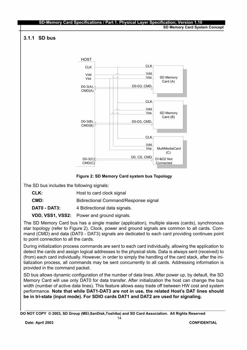
3.1.1 SD bus
Figure 2: SD Memory Card system bus Topology
The SD bus includes the following signals: CLK: Host to card clock signalCMD: Bidirectional Command/Response signalDAT0 - DAT3: 4 Bidirectional data signals.VDD, VSS1, VSS2: Power and ground signals.
The SD Memory Card bus has a single master (application), multiple slaves (cards), synchronousstar topology (refer to Figure 2). Clock, power and ground signals are common to all cards. Com-mand (CMD) and data (DAT0 - DAT3) signals are dedicated to each card providing continues pointto point connection to all the cards.During initialization process commands are sent to each card individually, allowing the application todetect the cards and assign logical addresses to the physical slots. Data is always sent (received) to(from) each card individually. However, in order to simply the handling of the card stack, after the ini-tialization process, all commands may be sent concurrently to all cards. Addressing information isprovided in the command packet. SD bus allows dynamic configuration of the number of data lines. After power up, by default, the SDMemory Card will use only DAT0 for data transfer. After initialization the host can change the buswidth (number of active data lines). This feature allows easy trade off between HW cost and systemperformance. Note that while DAT1-DAT3 are not in use, the related Host’s DAT lines shouldbe in tri-state (input mode). For SDIO cards DAT1 and DAT2 are used for signaling.
SD MemoryCard (A)
CLK
VddVss
D0-D3, CMD
SD MemoryCard (B)
CLK
VddVss
D0-D3, CMD
MultiMediaCard(C)
CLK
VddVss
D0, CS, CMD
CLK
VddVss
D0-3(A),CMD(A)
D0-3(B),CMD(B)
D0-3(C)CMD(C)
HOST
D1&D2 NotConnected

Tech
DO NOT COPY © 2003, SD Group (MEI,SanDisk,Toshiba) and SD Card Association. All Rights Reserved 15 hh
Date: April 2003 CONFIDENTIAL
SD-Memory Card Specifications / Part 1. Physical Layer Specification; Version 1.10 SD Memory Card System Concept
3.1.2 SPI bus
The SPI compatible communication mode of the SD Memory Card is designed to communicate witha SPI channel, commonly found in various microcontrollers in the market. The interface is selectedduring the first reset command after power up and cannot be changed as long as the part is pow-ered on. The SPI standard defines the physical link only, and not the complete data transfer protocol. The SDMemory Card SPI implementation uses the same command set of the SD mode. From the applica-tion point of view, the advantage of the SPI mode is the capability of using an off-the-shelf host,hence reducing the design-in effort to minimum. The disadvantage is the loss of performance, rela-tively to the SD mode which enables the wide bus option. The SD Memory Card SPI interface is compatible with SPI hosts available on the market. As anyother SPI device the SD Memory Card SPI channel consists of the following four signals:
CS: Host to card Chip Select signal.CLK: Host to card clock signalDataIn: Host to card data signal.DataOut: Card to host data signal.
Another SPI common characteristic are byte transfers, which is implemented in the card as well. Alldata tokens are multiples of bytes (8 bit) and always byte aligned to the CS signal.
Figure 3: SD Memory Card system (SPI mode) bus topology
The card identification and addressing methods are replaced by a hardware Chip Select (CS) sig-nal. There are no broadcast commands. For every command, a card (slave) is selected by asserting
SD MemoryCARD (A)(SPI mode)
VddVss
CLK,DataIN,DataOut
SD MemoryCARD (B)(SPI mode)
VddVss
MultiMediaCardCARD (C)(SPI mode)
VddVss
CLK,DataIN,DataOut
VddVss
CLK,DataIN,DataOut
HOST
CLK,DataIN,DataOut
CSCS(B)
CSCS(A)
CSCS(C)

DO NOT COPY © 2003, SD Group (MEI,SanDisk,Toshiba) and SD Card Association. All Rights Reserved 16 hh
Date: April 2003 CONFIDENTIAL
SD-Memory Card Specifications / Part 1. Physical Layer Specification; Version 1.10 SD Memory Card System Concept
(active low) the CS signal (see Figure 3).The CS signal must be continuously active for the duration of the SPI transaction (command,response and data). The only exception occurs during card programming, when the host can de-assert the CS signal without affecting the programming process. The SPI interface uses the 7 out of the SD 9 signals (DAT1 and DAT 2 are not used, DAT3 is the CSsignal) of the SD bus.
3.2 Bus Protocol
3.2.1 SD bus
Communication over the SD bus is based on command and data bit streams which are initiated by astart bit and terminated by a stop bit. • Command: a command is a token which starts an operation. A command is sent from the host
either to a single card (addressed command) or to all connected cards (broadcast command). A command is transferred serially on the CMD line.
• Response: a response is a token which is sent from an addressed card, or (synchronously) from all connected cards, to the host as an answer to a previously received command. A response is transferred serially on the CMD line.
• Data: data can be transferred from the card to the host or vice versa. Data is transferred via the data lines.
Figure 4: “no response” and “no data” operations
Card addressing is implemented using a session address, assigned to the card during the initializa-tion phase. The structure of commands, responses and data blocks is described in Chapter 4. Thebasic transaction on the SD bus is the command/response transaction (refer to Figure 4). This typeof bus transactions transfer their information directly within the command or response structure. Inaddition, some operations have a data token. Data transfers to/from the SD Memory Card are done in blocks. Data blocks always succeeded byCRC bits. Single and multiple block operations are defined. Note that the Multiple Block operationmode is better for faster write operation. A multiple block transmission is terminated when a stopcommand follows on the CMD line. Data transfer can be configured by the host to use single or mul-tiple data lines.
command command response
operation (no response) operation (no data)
CMD
DAT
from host
to card(s)
from host
to card
from card
to host

DO NOT COPY © 2003, SD Group (MEI,SanDisk,Toshiba) and SD Card Association. All Rights Reserved 17 hh
Date: April 2003 CONFIDENTIAL
SD-Memory Card Specifications / Part 1. Physical Layer Specification; Version 1.10 SD Memory Card System Concept
Figure 5: (Multiple) Block read operation
The block write operation uses a simple busy signaling of the write operation duration on the DAT0data line (see Figure 6) regardless of the number of data lines used for transferring the data.
Figure 6: (Multiple) Block write operation
Command tokens have the following coding scheme:
Figure 7: Command token format
Each command token is preceded by a start bit (‘0’) and succeeded by an end bit (‘1’). The totallength is 48 bits. Each token is protected by CRC bits so that transmission errors can be detectedand the operation may be repeated.
command response command response
block read operation data stop operation
CMD
DAT
from host
to card
stop command stops data transfer
data from card to host
from card
to host
data block crc data block crc data block crc
multiple block read operation
command response command response
block write operation data stop operation
CMD
DAT
from host
to card
stop command stops data trans-
fer
data from host
to card
from card
to host
data block crc data block crc
multiple block write operation
busy busy
crc ok response and busy
from card
0 1 CONTENT 1total length=48 bits
start bit:always’0’
transmitter bit:’1’= host command
end bit:always ‘1’
Command content: command and address information or parameter, protected by 7 bit CRC checksum
CRC

DO NOT COPY © 2003, SD Group (MEI,SanDisk,Toshiba) and SD Card Association. All Rights Reserved 18 hh
Date: April 2003 CONFIDENTIAL
SD-Memory Card Specifications / Part 1. Physical Layer Specification; Version 1.10 SD Memory Card System Concept
Response tokens have four coding schemes depending on their content. The token length is either48 or 136 bits. The detailed commands and response definition is given in Chapter 4.7. The CRCprotection algorithm for block data is a 16 bit CCITT polynomial. All used CRC types are describedin Chapter 4.5.
Figure 8: Response token format
In the CMD line the MSB bit is transmitted first the LSB bit is the last.when the wide bus option is used, the data is transferred 4 bits at a time (refer to Figure 9). Start andend bits, as well as the CRC bits, are transmitted for every one of the DAT lines. CRC bits are calcu-lated and checked for every DAT line individually. The CRC status response and Busy indication willbe sent by the card to the host on DAT0 only (DAT1-DAT3 during that period are don’t care).
There are two types of Data packet format for the SD card.(1) Usual data (8 bit width)The usual data (8 bit width) are sent in LSB (Least Significant Byte)first, MSB (Most Significant Byte) last manner. But in the individual byte it is MSB (Most Signifi-cant Bit) first, LSB (Least Significant Bit) last.(2) Wide width data (SD Memory Register)The wide width data is shifted from MSB bit.
0 0 CONTENT 1total length=48 bits
start bit:always’0’
transmitter bit:’0’=card response
end bit:always ‘1’
Response content: mirrored command and status infor-mation (R1 response), OCR register (R3 response) or
RCA (R6), protected by a 7bit CRC checksum
R1, R3,R6
0 0 CONTENT=CID or CSDtotal length=136 bits
R21
end bit:always ‘1’
CRC

DO NOT COPY © 2003, SD Group (MEI,SanDisk,Toshiba) and SD Card Association. All Rights Reserved 20 hh
Date: April 2003 CONFIDENTIAL
SD-Memory Card Specifications / Part 1. Physical Layer Specification; Version 1.10 SD Memory Card System Concept
3.2.2 SPI Bus
While the SD channel is based on command and data bit streams which are initiated by a start bitand terminated by a stop bit, the SPI channel is byte oriented. Every command or data block is builtof 8-bit bytes and is byte aligned to the CS signal (i.e. the length is a multiple of 8 clock cycles). Similar to the SD protocol, the SPI messages consist of command, response and data-block tokensAll communication between host and cards is controlled by the host (master). The host starts everybus transaction by asserting the CS signal low. The response behavior in the SPI mode differs from the SD mode in the following three aspects:• The selected card always responds to the command.• Two new (8 & 16 bit) response structure is used• When the card encounters a data retrieval problem, it will respond with an error response (which
replaces the expected data block) rather than by a time-out as in the SD mode.In addition to the command response, every data block sent to the card during write operations willbe responded with a special data response token.
• Data ReadSingle and multiple block read commands are supported in SPI mode. However, in order to complywith the SPI industry standard, only two (unidirectional) signal are used (refer to Chapter 10). Uponreception of a valid read command the card will respond with a response token followed by a datatoken of the length defined in a previous SET_BLOCKLEN (CMD16) command. A multiple blockread operation is terminated, similar to the SD protocol, with the STOP_TRANSMISSION com-mand.
Figure 10: Read operation
A valid data block is suffixed with a 16 bit CRC generated by the standard CCITT polynomialx16+x12+x5+1.In case of a data retrieval error, the card will not transmit any data. Instead, a special data errortoken will be sent to the host. Figure 11 shows a data read operation which terminated with an error
commandDataIn
DataOut
from host
to card
data from card to host
fromcard
to host
data blockresponse
command
stop Com-mand
CRC data block CRC response
block read operation data stop operation
multiple block read operation

DO NOT COPY © 2003, SD Group (MEI,SanDisk,Toshiba) and SD Card Association. All Rights Reserved 21 hh
Date: April 2003 CONFIDENTIAL
SD-Memory Card Specifications / Part 1. Physical Layer Specification; Version 1.10 SD Memory Card System Concept
token rather than a data block.
Figure 11: Read operation - data error
• Data Write Single and multiple block write operations are supported in SPI mode. Upon reception of a validwrite command, the card will respond with a response token and will wait for a data block to be sentfrom the host. CRC suffix, block length and start address restrictions are identical to the read opera-tion (see Figure 12).
Figure 12: Write operation
After a data block has been received, the card will respond with a data-response token. If the datablock has been received without errors, it will be programmed. As long as the card is busy program-ming, a continuous stream of busy tokens will be sent to the host (effectively holding the DataOutline low).
commandDataIn
DataOut
from host
to card
data error token from card to host
fromcard
to host
data errorresponse
command
Next Command
Data Resp
commandDataIn
DataOut
fromhost
to card
data from host
to card
from card
to host
data block
busy
Dataresponse and
busy from card
response
>
data start token
data from host
to card
data block>
Data Resp busy
<
data stop token
block write operation
data stop operation
multiple block write operation

DO NOT COPY © 2003, SD Group (MEI,SanDisk,Toshiba) and SD Card Association. All Rights Reserved 22 hh
Date: April 2003 CONFIDENTIAL
SD-Memory Card Specifications / Part 1. Physical Layer Specification; Version 1.10 SD Memory Card System Concept
3.3 SD Memory Card - Pins and Registers
The SD Memory Card has the form factor 24mm x 32mm x 2.1mm or 24mm x 32mm x 1.4mm.
Figure 13: SD Memory Card shape and interface (top view)
Figure 13 describes the general idea of the shape and interface contacts of SD Memory Card. Thedetailed physical dimensions and mechanical description is given in chapter 9.The following table defines the card contacts:
Each card has a set of information registers (see also Chapter 5 in the SD Memory Card Physical
Pin #SD Mode SPI Mode
Name Type1
1) S: power supply; I: input; O: output using push-pull drivers; PP: I/O using push-pull drivers;
Description Name Type Description
1 CD/DAT32
2) The extended DAT lines (DAT1-DAT3) are input on power up. They start to operate as DAT lines after SET_BUS_WIDTH command. The Host shall keep its own DAT1-DAT3 lines in input mode, as well, while they are not used. It is defined so, in order to keep compatibility to MultiMediaCards.
I/O/PP3
3) After power up this line is input with 50KOhm pull-up (can be used for card detection or SPI mode selec-tion). The pull-up should be disconnected by the user, during regular data transfer, with SET_CLR_CARD_DETECT (ACMD42) command
Card Detect / Data Line [Bit 3]
CS I Chip Select (neg true)
2 CMD PP Command/Response DI I Data In
3 VSS1 S Supply voltage ground VSS S Supply voltage ground 4 VDD S Supply voltage VDD S Supply voltage 5 CLK I Clock SCLK I Clock 6 VSS2 S Supply voltage ground VSS2 S Supply voltage ground 7 DAT0 I/O/PP Data Line [Bit 0] DO O/PP Data Out 8 DAT14
4) DAT1 line may be used as Interrupt Output (from the Card) in SDIO mode during all the times that it is not in use for data transfer operations (refer to "SDIO Card Specification" for further details).
I/O/PP Data Line [Bit 1] RSV9 DAT25
5) DAT2 line may be used as Read Wait signal in SDIO mode (refer to "SDIO Card Specification" for further details).
I/O/PP Data Line [Bit 2] RSV
Table 1: SD memory Card Pad Assignment
SD MemoryCard
1 2 3 45 6789
wp

DO NOT COPY © 2003, SD Group (MEI,SanDisk,Toshiba) and SD Card Association. All Rights Reserved 23 hh
Date: April 2003 CONFIDENTIAL
SD-Memory Card Specifications / Part 1. Physical Layer Specification; Version 1.10 SD Memory Card System Concept
Layer Specification):
The host may reset the cards by switching the power supply off and on again. Each card shall haveits own power-on detection circuitry which puts the card into a defined state after the power-on. Noexplicit reset signal is necessary. The cards can also be reset by sending the GO_IDLE (CMD0)command.
Figure 14: SD Memory Card architecture
Name Width DescriptionCID 128 Card identification number; card individual number for identification. Mandatory.
RCA1
1) RCA register is not used (available) in SPI mode.
16 Relative card address; local system address of a card, dynamically suggested by the card and approved by the host during initialization. Mandatory.
DSR 16 Driver Stage Register; to configure the card’s output drivers. Optional.CSD 128 Card Specific Data; information about the card operation conditions. MandatorySCR 64 SD Configuration Register; information about the SD Memory Card’s Special Fea-
tures capabilities. MandatoryOCR 32 Operation condition register. Mandatory.
Table 2: SD Memory Card registers
RCA[15:0]
CID[127:0]
DSR[15:0]
CSD[127:0]
Card interfacecontroller
Memory core
Memory core interface
CMD CLK DAT0
Pow
er o
n de
tect
ion
reset
Interface driver
VDD
OCR[31:0]
reset
SCR[63:0]
DAT1DAT2
CD/DAT3

DO NOT COPY © 2003, SD Group (MEI,SanDisk,Toshiba) and SD Card Association. All Rights Reserved 24 hh
Date: April 2003 CONFIDENTIAL
SD-Memory Card Specifications / Part 1. Physical Layer Specification; Version 1.10 SD Memory Card System Concept
3.4 Compatibility to MultiMediaCard
The SD Memory Card protocol is designed to be a super-set of the MultiMediaCard protocol. Forcomplete details refer to MultiMedia card specification.

DO NOT COPY © 2003, SD Group (MEI,SanDisk,Toshiba) and SD Card Association. All Rights Reserved 25 hh
Date: April 2003
SD-Memory Card Specifications / Part 1. Physical Layer Specification; Version 1.10 SD Memory Card Functional Description
4 SD Memory Card Functional Description
4.1 General
All communication between host and cards is controlled by the host (master). The host sends com-mands of two types: broadcast and addressed (point-to-point) commands.• Broadcast commandsBroadcast commands are intended for all cards. Some of these commands require a response.• Addressed (point-to-point) commands The addressed commands are sent to the addressed card and cause a response from this card.A general overview of the command flow is shown in Figure 15 for the card identification mode andin Figure for the data transfer mode. The commands are listed in the command tables (Table 9 -Table 17). The dependencies between current state, received command and following state arelisted in Table 19. In the following sections, the different card operation modes will be described first.Thereafter, the restrictions for controlling the clock signal are defined. All SD Memory Card com-mands together with the corresponding responses, state transitions, error conditions and timingsare presented in the succeeding sections. Two operation modes are defined for the SD Memory Card system (host and cards):• Card identification mode
The host will be in card identification mode after reset and while it is looking for new cards on the bus. Cards will be in this mode after reset until the SEND_RCA command (CMD3) is received (in case of MultiMediaCard - SET_RCA command).
• Data transfer modeCards will enter data transfer mode once their RCA is first published. The host will enter data transfer mode after identifying all the cards on the bus.
The following table shows the dependencies between operation modes and card states. Each statein the SD Memory Card state diagram (see Figure 15 and Figure ) is associated with one operationmode:
Card state Operation modeInactive State inactiveIdle State
card identification modeReady StateIdentification StateStand-by State
data transfer mode
Transfer StateSending-data StateReceive-data StateProgramming StateDisconnect State
Table 3: Overview of Card States vs. Operation modes
DO NOT COPY © 2003, SD Group (MEI,SanDisk,Toshiba) and SD Card Association. All Rights Reserved 26 hh
Date: April 2003 CONFIDENTIAL
SD-Memory Card Specifications / Part 1. Physical Layer Specification; Version 1.10 SD Memory Card Functional Description
4.2 Card Identification Mode
While in card identification mode the host resets all the cards that are in card identification mode,validates operation voltage range, identifies cards and asks them to publish Relative Card Address(RCA). This operation is done to each card separately on its own CMD line. All data communicationin the Card Identification Mode uses the command line (CMD) only.
4.2.1 Card Reset
The command GO_IDLE_STATE (CMD0) is the software reset command and sets each card intoIdle State regardless of the current card state. Cards in Inactive State are not affected by this com-mand.After power-on by the host, all cards are in Idle State, including the cards that have been in InactiveState before.After power-on or CMD0, all cards’ CMD lines are in input mode, waiting for start bit of the next com-mand. The cards are initialized with a default relative card address (RCA=0x0000) and with adefault driver stage register setting (lowest speed, highest driving current capability).
4.2.2 Operating Voltage Range Validation
All cards shall be able to establish communication with the host using any operating voltage in themaximal allowed voltage range specified in this standard (see Chapter 6.6). However, the supportedminimum and maximum values for VDD are defined in the Operation Conditions Register (OCR) andmay not cover the whole range. Cards that store the CID and CSD data in the payload memorywould be able to communicate these information only under data transfer VDD conditions. Thatmeans if host and card have non compatible VDD ranges, the card will not be able to complete theidentification cycle, nor to send CSD data.Therefore, a special command SD_SEND_OP_COND (ACMD41) is designed to provide SD Mem-ory Card hosts with a mechanism to identify and reject cards which do not match the VDD rangedesired by the host. This is accomplished by the host sending the required VDD voltage window asthe operand of this command (See Chapter 5.1). Cards which can not perform data transfer in thespecified range must discard themselves from further bus operations and go into Inactive State. Thelevels in the OCR register shall be defined accordingly (see Chapter 5.1). Note that ACMD41 isapplication specific command, therefore APP_CMD (CMD55) shall always precede ACMD41. TheRCA to be used for CMD55 in idle_state shall be the card’s default RCA = 0x0000. The MultiMediaCard will not respond to ACMD41 (actually it will not respond to APP_CMD -CMD55, that preceding it). MultiMediaCard shall be initialized as per the MultiMediaCard spec,using SEND_OP_COND command (CMD1 of MultiMediaCard). The host should ignore anILLEGAL_COMMAND status in the MultiMediaCard response to CMD3, as it is a residue ofACMD41 which is invalid in MultiMediaCard (CMD0, 1, 2 do not clear the status register). Actually,ACMD41 and CMD1 will be used by the host to distinguish between MultiMediaCard and SD Mem-ory Cards in a system.

DO NOT COPY © 2003, SD Group (MEI,SanDisk,Toshiba) and SD Card Association. All Rights Reserved 27 hh
Date: April 2003 CONFIDENTIAL
SD-Memory Card Specifications / Part 1. Physical Layer Specification; Version 1.10 SD Memory Card Functional Description
Figure 15: SD Memory Card state diagram (card identification mode)
By omitting the voltage range in the command, the host can query each card and determine thecommon voltage range before sending out-of-range cards into the Inactive State. This query shouldbe used if the host is able to select a common voltage range or if a notification to the application ofnon usable cards in the stack is desired. Afterwards, the host must choose a voltage for operationand reissue ACMD41 with this condition, sending incompatible cards into the Inactive State.The busy bit in the ACMD41 response can be used by a card to tell the host that it is still working onits power-up/reset procedure (e.g. downloading the register information from memory field) and isnot ready yet for communication. In this case the host must repeat ACMD41 until the busy bit iscleared.During the initialization procedure, the host is not allowed to change the operating voltage range.Such changes shall be ignored by the card. If there is a real change in the operating conditions, thehost must reset the card stack (sending CMD0 to all cards) and restart the initialization procedure.However, for accessing also the cards being already in Inactive State, a hard reset must be done byswitching the power supply off and on.The command GO_INACTIVE_STATE (CMD15) can be used to send an addressed card into the
ACMD41 InactiveState (ina)
Idle State(idle)
IdentificationState (ident)
CMD0
CMD3
from all states except (ina)
from all states in
CMD15
cards with non compatible voltage range
card is busy or
data-transfer-modeStand-by State
(stby)
Power on
host omitted voltagerange
CMD3
Card responds withnew RCA
Card responds withnew RCA
Ready State(ready)
CMD2
data-transfer mode
card-identification mode
Start MultiMediaCard
(Non valid command)Must be a MultiMediaCard
initialization processstarting at CMD1
No Response
SPI OperationMode
CMD0 + CS Asserted (“0”)

DO NOT COPY © 2003, SD Group (MEI,SanDisk,Toshiba) and SD Card Association. All Rights Reserved 28 hh
Date: April 2003 CONFIDENTIAL
SD-Memory Card Specifications / Part 1. Physical Layer Specification; Version 1.10 SD Memory Card Functional Description
Inactive State. This command is used when the host explicitly wants to deactivate a card (e.g. hostis changing VDD into a range which is known to be not supported by this card).
4.2.3 Card Identification Process
The host starts the card identification process with the identification clock rate fOD (see Chapter 6.8).In SD Memory Card the CMD line output drives are push-pull drivers. After the bus is activated the host will request the cards to send their valid operation conditions(ACMD41 preceding with APP_CMD - CMD55 with RCA=0x0000). The response to ACMD41 is theoperation condition register of the card. The same command shall be send to all of the new cards inthe system. Incompatible cards are sent into Inactive State. The host then issues the commandALL_SEND_CID (CMD2), to each card to get its unique card identification (CID) number. Card thatis unidentified (i.e. which is in Ready State) sends its CID number as the response (on the CMDline). After the CID was sent by the card it goes into Identification State. Thereafter, the host issuesCMD3 (SEND_RELATIVE_ADDR) asks the card to publish a new relative card address (RCA),which is shorter than CID and which will be used to address the card in the future data transfermode (typically with a higher clock rate than fOD). Once the RCA is received the card state changesto the Stand-by State. At this point, if the host wants that the card will have another RCA number, itmay ask the card to publish a new number by sending another SEND_RELATIVE_ADDR commandto the card. The last published RCA is the actual RCA number of the card.The host repeats the identification process, i.e. the cycles with CMD2 and CMD3 for each card inthe system.After all the SD Memory Cards were initialized the host shall initialize the MultiMediaCards that arein the system (if any), using the CMD2 and CMD3 as given in the MultiMediaCard spec. Note that inthe SD system all the cards are connected separately so each MultiMediaCard shall be initializedindividually.
4.3 Data Transfer ModeUntil the end of Card Identification Mode the host must remain at fOD frequency because somecards may have operating frequency restrictions during the card identification mode. In Data Trans-fer Mode the host may operate the card in fPP frequency range (see chapter 6.8). The host issuesSEND_CSD (CMD9) to obtain the Card Specific Data (CSD register), e.g. block length, card storagecapacity, etc.
The broadcast command SET_DSR (CMD4) configures the driver stages of all identified cards. Itprograms their DSR registers corresponding to the application bus layout (length) and the numberof cards on the bus and the data transfer frequency. The clock rate is also switched from fOD to fPP atthat point. SET_DSR command is an option for the card and the host.
CMD7 is used to select one card and put it into the Transfer State. Only one card can be in theTransfer State at a given time. If a previously selected card is in the Transfer State its connectionwith the host is released and it will move back to the Stand-by State. When CMD7 is issued with thereserved relative card address “0x0000”, all cards are put back to Stand-by State (Note that it is the

DO NOT COPY © 2003, SD Group (MEI,SanDisk,Toshiba) and SD Card Association. All Rights Reserved 29 hh
Date: April 2003 CONFIDENTIAL
SD-Memory Card Specifications / Part 1. Physical Layer Specification; Version 1.10 SD Memory Card Functional Description
Figure 16: SD Memory Card state diagram (data transfer mode)
responsibility of the Host to reserve the RCA=0 for card de-selection - refer to Table 9, CMD7 description). This may be used before identifying new cards without resetting other already regis-tered cards. Cards which already have an RCA do not respond to identification commands(ACMD41, CMD2, see Chapter 4.2.3) in this state.
Important Note: The card de-selection is done if certain card gets CMD7 with un-matched RCA.That happens automatically if selection is done to another card and the CMD lines are common. So,in SD Memory Card system it will be the responsibility of the host either to work with common CMDline (after initialization is done) - in that case the card de-selection will be done automatically (as inMultiMediaCard system) or if the CMD lines are separate then the host shall be aware to the neces-sity to de-select cards.
All data communication in the Data Transfer Mode is point-to point between the host and theselected card (using addressed commands). All addressed commands get acknowledged by aresponse on the CMD line.
State (tran)Stand-by State
(stby)Transfer
Sending-dataState (data)
CMD3
CMD4,
CMD7
9,10,3
CMD16,
CMD7
CMD6,17,18,30,56(r)ACMD13,22,51
data transfer
card identification
CMD13, CMD55
in data-transfer-modeno state transition
CMD12,“operation
32..37
State (rcv)Receive-data
CMD24,25,26,27,42,56(w)
CMD15
from all states indata-transfer-mode
State (prg)Programming
CMD28,29,38
“operation complete”
State (dis)Disconnect
CMD7
“operation complete”
CMD0
CMD7
complete”
CMD12 or„transfer end“
mode
mode
ACMD6,42ACMD23

DO NOT COPY © 2003, SD Group (MEI,SanDisk,Toshiba) and SD Card Association. All Rights Reserved 30 hh
Date: April 2003 CONFIDENTIAL
SD-Memory Card Specifications / Part 1. Physical Layer Specification; Version 1.10 SD Memory Card Functional Description
The relationship between the various data transfer modes is summarized below (see Figure ):
• All data read commands can be aborted any time by the stop command (CMD12). The datatransfer will terminate and the card will return to the Transfer State. The read commands are:block read (CMD17), multiple block read (CMD18), send write protect (CMD30), send scr(ACMD51) and general command in read mode (CMD56).
• All data write commands can be aborted any time by the stop command (CMD12). The writecommands must be stopped prior to deselecting the card by CMD7. The write commands are:block write (CMD24 and CMD25), write CID (CMD26), write CSD (CMD27), lock/unlock com-mand (CMD42) and general command in write mode (CMD56).
• As soon as the data transfer is completed, the card will exit the data write state and move eitherto the Programming State (transfer is successful) or Transfer State (transfer failed).
• If a block write operation is stopped and the block length and CRC of the last block are valid, thedata will be programmed.
• The card may provide buffering for block write. This means that the next block can be sent to thecard while the previous is being programmed.If all write buffers are full, and as long as the card is in Programming State (see SD Memory Cardstate diagram Figure ), the DAT0 line will be kept low (BUSY).
• There is no buffering option for write CSD, write CID, write protection and erase. This means thatwhile the card is busy servicing any one of these commands, no other data transfer commandswill be accepted. DAT0 line will be kept low as long as the card is busy and in the ProgrammingState. Actually if the CMD and DAT0 lines of the cards are kept separated and the host keep thebusy DAT0 line disconnected from the other DAT0 lines (of the other cards) the host may accessthe other cards while the card is in busy.
• Parameter set commands are not allowed while card is programming. Parameter set commands are: set block length (CMD16), erase block start (CMD32) and eraseblock end (CMD33).
• Read commands are not allowed while card is programming.• Moving another card from Stand-by to Transfer State (using CMD7) will not terminate erase and
programming operations. The card will switch to the Disconnect State and will release the DATline.
• A card can be reselected while in the Disconnect State, using CMD7. In this case the card willmove to the Programming State and reactivate the busy indication.
• Resetting a card (using CMD0 or CMD15) will terminate any pending or active programmingoperation. This may destroy the data contents on the card. It is the host’s responsibility to pre-vent this.
4.3.1 Wide Bus Selection/Deselection
Wide Bus (4 bit bus width) operation mode may be selected/deselected using ACMD6. The defaultbus width after power up or GO_IDLE (CMD0) is 1 bit bus width. ACMD6 command is valid in ‘transtate‘ only. That means that the bus width may be changed only after a card was selected (CMD7).

DO NOT COPY © 2003, SD Group (MEI,SanDisk,Toshiba) and SD Card Association. All Rights Reserved 31 hh
Date: April 2003 CONFIDENTIAL
SD-Memory Card Specifications / Part 1. Physical Layer Specification; Version 1.10 SD Memory Card Functional Description
4.3.2 Data Read
The DAT bus line level is high by the pull-up when no data is transmitted. A transmitted data blockconsists of start bits (1 or 4 bits LOW), followed by a continuous data stream. The data stream con-tains the payload data (and error correction bits if an off-card ECC is used). The data stream endswith end bits (1 or 4 bits HIGH) (see Figure 26-Figure 28). The data transmission is synchronous tothe clock signal. The payload for block oriented data transfer is protected by 1 or 4 bits CRC checksum (see Chapter 3.2). The Read operation from SD Memory Card may be interrupted by turning the power off. The SDMemory Card ensures that data is not destroyed during all the conditions except write or eraseoperations issued by the host even in the event of sudden shut down or removal.
• Block ReadBlock read is block oriented data transfer. The basic unit of data transfer is a block whose maximumsize is defined in the CSD (READ_BL_LEN). Smaller blocks whose starting and ending address areentirely contained within one physical block (as defined by READ_BL_LEN) may also be transmit-ted. It is a mandatory requirement that SD Memory Card shall have a capability to transfer blocks of512 Bytes.A CRC is appended to the end of each block ensuring data transfer integrity. CMD17(READ_SINGLE_BLOCK) initiates a block read and after completing the transfer, the card returnsto the Transfer State. CMD18 (READ_MULTIPLE_BLOCK) starts a transfer of several consecutiveblocks. Blocks will be continuously transferred until a STOP_TRANSMISSION command (CMD12)is issued. The stop command has an execution delay due to the serial command transmission. Thedata transfer stops after the end bit of the stop command.If the host uses partial blocks whose accumulated length is not block aligned and block misalign-ment is not allowed, the card shall detect a block misalignment at the beginning of the first mis-aligned block, set the ADDRESS_ERROR error bit in the status register, abort transmission andwait in the Data State for a stop command.
4.3.3 Data Write
The data transfer format is similar to the data read format. For block oriented write data transfer, theCRC check bits are added to each data block. The card performs 1 or 4 bits CRC parity check (seeChapter 4.5) for each received data block prior to the write operation. By this mechanism, writing oferroneously transferred data can be prevented.
• Block WriteDuring block write (CMD24 - 27,42,56(w)) one or more blocks of data are transferred from the hostto the card with 1 or 4 bits CRC appended to the end of each block by the host. A card supportingblock write shall always be able to accept a block of data defined by WRITE_BL_LEN and its512bytes derivatives (for example: If write block length=1024bytes then write blocks of 1024 and512bytes are supported). If WRITE_BL_PARTIAL is allowed (=1) then smaller blocks, up to resolu-tion of one byte, can be used as well. If the CRC fails, the card shall indicate the failure on the DATline (see below); the transferred data will be discarded and not written, and all further transmittedblocks (in multiple block write mode) will be ignored.Multiple block write command shall be used rather than continuous single write command to makefaster write operation.If the host uses partial blocks whose accumulated length is not block aligned and block misalign-

DO NOT COPY © 2003, SD Group (MEI,SanDisk,Toshiba) and SD Card Association. All Rights Reserved 32 hh
Date: April 2003 CONFIDENTIAL
SD-Memory Card Specifications / Part 1. Physical Layer Specification; Version 1.10 SD Memory Card Functional Description
ment is not allowed (CSD parameter WRITE_BLK_MISALIGN is not set), the card shall detect theblock misalignment error and abort programming before the beginning of the first misaligned block.The card shall set the ADDRESS_ERROR error bit in the status register, and while ignoring all fur-ther data transfer, wait in the Receive-data-State for a stop command.The write operation shall also be aborted if the host tries to write over a write protected area. In thiscase, however, the card shall set the WP_VIOLATION bit.Programming of the CID and CSD registers does not require a previous block length setting. Thetransferred data is also CRC protected. If a part of the CSD or CID register is stored in ROM, thenthis unchangeable part must match the corresponding part of the receive buffer. If this match fails,then the card will report an error and not change any register contents.Some cards may require long and unpredictable times to write a block of data. After receiving ablock of data and completing the CRC check, the card will begin writing and hold the DAT0 line lowif its write buffer is full and unable to accept new data from a new WRITE_BLOCK command. Thehost may poll the status of the card with a SEND_STATUS command (CMD13) at any time, and thecard will respond with its status. The status bit READY_FOR_DATA indicates whether the card canaccept new data or whether the write process is still in progress). The host may deselect the card byissuing CMD7 (to select a different card) which will displace the card into the Disconnect State andrelease the DAT line without interrupting the write operation. When reselecting the card, it will reac-tivate busy indication by pulling DAT to low if programming is still in progress and the write buffer isunavailable. Actually, the host may perform simultaneous write operation to several cards with inter-leaving process. The interleaving process can be done by accessing each card separately whileother cards are in busy. This process can be done by proper CMD and DAT0-3 line manipulations(disconnection of busy cards).
• Pre-erase setting prior to a multiple block write operationSetting a number of write blocks to be pre_erased (ACMD23) will make a following Multiple Block Write operation faster compared to the same operation without preceding ACMD23. The host will use this command to define how many number of write blocks are going to be send in the next write operation. If the host will terminate the write operation (Using stop transmission) before all the data blocks sent to the card the content of the remaining write blocks is undefined(can be either erased or still have the old data). If the host will send more number of write blocks than defined in ACMD23 the card will erase block one by one(as new data is received). This number will be reset to the default(=1) value after Multiple Blocks Write operation.It is recommended using this command preceding CMD25, some of the cards will be faster for Mul-tiple Write Blocks operation. Note that The host must send ACMD23 just before WRITE command ifthe host wants to use the pre-erase feature. If not, pre-erase-count might be cleared automaticallywhen another commands (ex: Security Aplication Commands) are executed.
• Send Number of Written BlocksSystems that use PipeLine mechanism for data buffers management are, in some cases, unable todetermine which block was the last to be well written to the flash if an error occurs in the middle of aMultiple Blocks Write operation. The card will respond to ACMD22 with the number of well writtenblocks.
4.3.4 Erase
It is desirable to erase many write blocks simultaneously in order to enhance the data throughput.

DO NOT COPY © 2003, SD Group (MEI,SanDisk,Toshiba) and SD Card Association. All Rights Reserved 33 hh
Date: April 2003 CONFIDENTIAL
SD-Memory Card Specifications / Part 1. Physical Layer Specification; Version 1.10 SD Memory Card Functional Description
Identification of these write blocks is accomplished with the ERASE_WR_BLK_START(CMD32),ERASE_WR_BLK_END(CMD33) commands. The host must adhere to the following command sequence: ERASE_WR_BLK_START,ERASE_WR_BLK_END and ERASE (CMD38).If an erase (CMD38) or address setting (CMD32, 33) command is received out of sequence, thecard shall set the ERASE_SEQ_ERROR bit in the status register and reset the whole sequence.If an out of sequence command (except SEND_STATUS) is received, the card shall set theERASE_RESET status bit in the status register, reset the erase sequence and execute the lastcommand.If the erase range includes write protected sectors, they shall be left intact and only the non pro-tected sectors shall be erased. The WP_ERASE_SKIP status bit in the status register shall be set.The address field in the address setting commands is a write block address in byte units. The cardwill ignore all LSB’s below the WRITE_BL_LEN (see CSD) size.As described above for block write, the card will indicate that an erase is in progress by holdingDAT0 low. The actual erase time may be quite long, and the host may issue CMD7 to deselect thecard or perform card disconnection, as described in the Block Write section, above.The data at the card after an erase operation is either ‘0’ or ‘1’, depends on the card vendor.The SCR register bit DATA_STAT_AFTER_ERASE (bit 55) defines whether it is ‘0’ or ‘1’.
4.3.5 Write Protect Management
Three write protect methods are supported in the SD Memory Card as follows:- Mechanical write protect switch (Host responsibility only)- Card internal write protect (Card’s responsibility)- Password protection card lock operation.
• Mechanical Write Protect SwitchA mechanical sliding tablet on the side of the card (refer to the mechanical description Chapter 7)will be used by the user to indicate that a given card is write protected or not. If the sliding tablet ispositioned in such a way that the window is open it means that the card is write protected. If the win-dow is close the card is not write protected. A proper, matched, switch on the socket side will indicate to the host that the card is write protectedor not. It is the responsibility of the host to protect the card. The position of the write protect switch isun-known to the internal circuitry of the card.
• Card’s Internal Write Protection (Optional)Card data may be protected against either erase or write. The entire card may be permanently writeprotected by the manufacturer or content provider by setting the permanent or temporary write pro-tect bits in the CSD. For cards which support write protection of groups of sectors by setting theWP_GRP_ENABLE bit in the CSD, portions of the data may be protected (in units ofWP_GRP_SIZE sectors as specified in the CSD), and the write protection may be changed by theapplication. The SET_WRITE_PROT command sets the write protection of the addressed write-pro-tect group, and the CLR_WRITE_PROT command clears the write protection of the addressedwrite-protect group. The SEND_WRITE_PROT command is similar to a single block read command. The card shall

DO NOT COPY © 2003, SD Group (MEI,SanDisk,Toshiba) and SD Card Association. All Rights Reserved 34 hh
Date: April 2003 CONFIDENTIAL
SD-Memory Card Specifications / Part 1. Physical Layer Specification; Version 1.10 SD Memory Card Functional Description
send a data block containing 32 write protection bits (representing 32 write protect groups starting atthe specified address) followed by 16 CRC bits. The address field in the write protect commands isa group address in byte units. The card will ignore all LSB’s below the group size.The Password Card Lock protection is described in the following section.
4.3.6 Card Lock/Unlock Operation (Optional)
The password protection feature enables the host to lock a card while providing a password, whichlater will be used for unlocking the card. The password and its size is kept in an 128 bit PWD and 8bit PWD_LEN registers, respectively. These registers are non-volatile so that a power cycle will noterase them. Locked cards respond to (and execute) all commands in the "basic" command class (class 0),ACMD41 and “lock card” command class. Thus the host is allowed to reset, initialize, select, queryfor status, etc., but not to access data on the card. If the password was previously set (the value ofPWD_LEN is not ‘0’) will be locked automatically after power on.Similar to the existing CSD and CID register write commands the lock/unlock command is availablein "transfer state" only. This means that it does not include an address argument and the card has tobe selected before using it.The card lock/unlock command has the structure and bus transaction type of a regular single blockwrite command. The transferred data block includes all the required information of the command(password setting mode, PWD itself, card lock/unlock etc.). The following table describes the struc-ture of the command data block.
• ERASE: ‘1’ Defines Forced Erase Operation (all other bits shall be ‘0’) and only the cmd byte is sent.• LOCK/UNLOCK: ‘1’ = Locks the card. ‘0’ = Unlock the card (note that it is valid to set this bit
together with SET_PWD but it is not allowed to set it together with CLR_PWD).• CLR_PWD: ‘1’ = Clears PWD.• SET_PWD: ‘1’ = Set new password to PWD• PWDS_LEN: Defines the following password/s length (in bytes). In case of Password change,
this field include the total password lengths of old and new passwords.• PWD: In case of set new password contains the new password. In case of password
change it contains the old password followed by new password. All other com-mands it contains the current password.
The data block size shall be defined by the host before it sends the card lock/unlock command. Thiswill allow different password sizes. The following paragraphs define the various lock/unlock command sequences:
Byte # Bit 7 Bit 6 Bit 5 Bit 4 Bit 3 Bit 2 Bit 1 Bit 00 Reserved ERASE LOCK_
UNLOCKCLR_PWD
SET_PWD
1 PWDS_LEN2
Password data...PWDS_LEN + 1
Table 4: Lock card data structure
DO NOT COPY © 2003, SD Group (MEI,SanDisk,Toshiba) and SD Card Association. All Rights Reserved 35 hh
Date: April 2003 CONFIDENTIAL
SD-Memory Card Specifications / Part 1. Physical Layer Specification; Version 1.10 SD Memory Card Functional Description
• Setting the Password• Select a card (CMD7), if not previously selected already• Define the block length (CMD16), given by the 8bit card lock/unlock mode, the 8 bits pass-
word size (in bytes), and the number of bytes of the new password. In case that a pass-word replacement is done, then the block size shall consider that both passwords, the oldand the new one, are sent with the command.
• Send Card Lock/Unlock command with the appropriate data block size on the data lineincluding 16 bit CRC. The data block shall indicate the mode (SET_PWD), the length(PWDS_LEN) and the password itself. In case that a password replacement is done, thenthe length value (PWDS_LEN) shall include both passwords, the old and the new one, andthe PWD field shall include the old password (currently used) followed by the new pass-word. Note that card shall handle internally the calculation of the new password length bysubscribing the old password length from PWDS_LEN field.
• In case that the sent old password is not correct (not equal in size and content) thenLOCK_UNLOCK_FAILED error bit will be set in the status register and the old passworddoes not change. In case that PWD matches the sent old password then the given newpassword and its size will be saved in the PWD and PWDS_LEN fields, respectively.
Note that the password length register (PWD_LEN) indicates if a password is currently set. When itequals ‘0’ there is no password set. If the value of PWD_LEN is not equal to zero the card will lockitself after power up. It is possible to lock the card immediately in the current power session by set-ting the LOCK/UNLOCK bit (while setting the password) or sending additional command for cardlock.
• Reset the Password:• Select a card (CMD7), if not previously selected already• Define the block length (CMD16), given by the 8 bit card lock/unlock mode, the 8 bit pass-
word size (in bytes), and the number of bytes of the currently used password.• Send the card lock/unlock command with the appropriate data block size on the data line
including 16 bit CRC. The data block shall indicate the mode CLR_PWD, the length(PWDS_LEN) and the password (PWD) itself (LOCK/UNLOCK bit is don’t care). If thePWD and PWD_LEN content match the sent password and its size, then the content of thePWD register is cleared and PWD_LEN is set to 0. If the password is not correct then theLOCK_UNLOCK_FAILED error bit will be set in the status register.
• Locking a card:• Select a card (CMD7), if not previously selected already• Define the block length (CMD16), given by the 8 bit card lock/unlock mode, the 8 bit pass-
word size (in bytes), and the number of bytes of the currently used password.• Send the card lock/unlock command with the appropriate data block size on the data line
including 16 bit CRC. The data block shall indicate the mode LOCK, the length(PWDS_LEN) and the password (PWD) itself .
If the PWD content equals to the sent password then the card will be locked and the card-lockedstatus bit will be set in the status register. If the password is not correct thenLOCK_UNLOCK_FAILED error bit will be set in the status register.Note that it is possible to set the password and to lock the card in the same sequence. In such casethe host shall perform all the required steps for setting the password (as described above) includingthe bit LOCK set while the new password command is sent.If the password was previously set (PWD_LEN is not ‘0’), then the card will be locked automaticallyafter power on reset.

DO NOT COPY © 2003, SD Group (MEI,SanDisk,Toshiba) and SD Card Association. All Rights Reserved 36 hh
Date: April 2003 CONFIDENTIAL
SD-Memory Card Specifications / Part 1. Physical Layer Specification; Version 1.10 SD Memory Card Functional Description
An attempt to lock a locked card or to lock a card that does not have a password will fail and theLOCK_UNLOCK_FAILED error bit will be set in the status register, unless it was done during apassword definition or change operations.
• Unlocking the card:• Select a card (CMD7), if not previously selected already.• Define the block length (CMD16), given by the 8 bit card lock/unlock mode, the 8 bit pass-
word size (in bytes), and the number of bytes of the currently used password.• Send the card lock/unlock command with the appropriate data block size on the data line
including 16 bit CRC. The data block shall indicate the mode UNLOCK, the length(PWDS_LEN) and the password (PWD) itself.
If the PWD content equals to the sent password then the card will be unlocked and the card-lockedstatus bit will be cleared in the status register. If the password is not correct then theLOCK_UNLOCK_FAILED error bit will be set in the status register.Note that the unlocking is done only for the current power session. As long as the PWD is notcleared the card will be locked automatically on the next power up. The only way to unlock the cardis by clearing the password.An attempt to unlock an unlocked card will fail and LOCK_UNLOCK_FAILED error bit will be set inthe status register, unless it was done during a password definition or change operations.
• Forcing Erase:In case that the user forgot the password (the PWD content) it is possible to erase all the card datacontent along with the PWD content. This operation is called Forced Erase.
• Select a card (CMD7), if not previously selected already.• Define the block length (CMD16) to 1 byte (8bit card lock/unlock command). Send the card
lock/unlock command with the appropriate data block of one byte on the data line including16 bit CRC. The data block shall indicate the mode ERASE (the ERASE bit shall be theonly bit set).
If the ERASE bit is not the only bit in the data field then the LOCK_UNLOCK_FAILED error bit willbe set in the status register and the erase request is rejected. If the command was accepted thenALL THE CARD CONTENT WILL BE ERASED including the PWD and PWD_LEN register contentand the locked card will get unlocked. An attempt to force erase on an unlocked card will fail andLOCK_UNLOCK_FAILED error bit will be set in the status register.
4.3.7 Copyright Protection
Detailed description of the Copyrights Protection mechanism and the related security SD MemoryCard commands can be found in “SD Memory Card Security Specification” document. All the SDMemory Card security related commands shall be operated in data transfer mode of operation.As defined in the SDMI spec the data content that is saved in the card is saved already encryptedand it pass transparently to/from the card. NO operation is done on the data and there is no restric-tion to read the data at any time. Associated to every data packet (song, for example) that is savedin the un-protected memory there is a special data that shall be saved in a protected memory area.For any access (any Read or Write or Erase Command) from/to the data in the protected area, anauthentication procedure shall be done between the card and the connected device, either the LCM(PC for example) or the PD (Portable Device - SD Player for example). After the authentication pro-cess was passed OK, the card is ready to accept or give data from/to the connected device. Whilethe card is in the secured mode of operation (after the authentication succeeded) the argument and

DO NOT COPY © 2003, SD Group (MEI,SanDisk,Toshiba) and SD Card Association. All Rights Reserved 37 hh
Date: April 2003 CONFIDENTIAL
SD-Memory Card Specifications / Part 1. Physical Layer Specification; Version 1.10 SD Memory Card Functional Description
the associated data that is sent to the card or read from the card are encrypted. At the end of theRead/Write/Erase operation the card gets out automatically of its secured mode.
4.3.8 Application specific commands:
The SD Memory Card is defined to be protocol forward compatible to the MultiMediaCard Standard.The SD Memory Card system is designed to provide a standard interface for a variety applicationstypes. In order to keep future compatibility to the MultiMediaCard standard together with new SDMemory Card specific commands the SD Memory Card use the Application Specific commands fea-ture to implement its proprietary commands. Following is a description of the APP_CMD andGEN_CMD as were defined in the MultiMediaCard spec.
• Application Specific Command – APP_CMD (CMD55)This command, when received by the card, will cause the card to interpret the following commandas an application specific command, ACMD. The ACMD has the same structure as of regular Multi-MediaCard standard commands and it may have the same CMD number. The card will recognize itas ACMD by the fact that it appears after APP_CMD. The only effect of the APP_CMD is that if the command index of the, immediately, following com-mand has an ACMD overloading it, the non standard version will be used. If, as an example, a cardhas a definition for ACMD13 but not for ACMD7 then, if received immediately after APP_CMD com-mand, Command 13 will be interpreted as the non standard ACMD13 but, command 7 as the stan-dard CMD7. In order to use one of the manufacturer specific ACMD’s the host will: • Send APP_CMD. The response will have the APP_CMD bit (new status bit) set signaling to the
host that ACMD is now expected.• Send the required ACMD. The response will have the APP_CMD bit set, indicating that the
accepted command was interpreted as ACMD. If a non-ACMD is sent then it will be respectedby the card as normal SD Memory Card command and the APP_CMD bit in the Card Statusstays clear.
If a non valid command is sent (neither ACMD nor CMD) then it will be handled as a standard SDMemory Card illegal command error.From the SD Memory Card protocol point of view the ACMD numbers will be defined by the manu-facturers with some restrictions. The following ACMD numbers are reserved for the SD MemoryCard proprietary applications and may not be used by any SD Memory Card manufacturer:ACMD6, ACMD13, ACMD17-25, ACMD38-49, ACMD51.
• General Command - GEN_CMD (CMD56)The bus transaction of the GEN_CMD is the same as the single block read or write commands(CMD24 or CMD17). The difference is that the argument denotes the direction of the data transfer(rather than the address) and the data block is not a memory payload data but has a vendor specificformat and meaning. The card shall be selected (‘tran_state’) before sending CMD56. The datablock size is the BLOCK_LEN that was defined with CMD16. The response to CMD56 will be R1.Note that there are no reserved data pattern (of the associated data block) for SD Memory Cardspecific applications.

DO NOT COPY © 2003, SD Group (MEI,SanDisk,Toshiba) and SD Card Association. All Rights Reserved 38 hh
Date: April 2003 CONFIDENTIAL
SD-Memory Card Specifications / Part 1. Physical Layer Specification; Version 1.10 SD Memory Card Functional Description
4.3.9 Switch function command
Switch function command (CMD6)1 is used to switch or expand memory card functions. Currentlythere are two function groups defined:• Card access mode - 12.5MB/sec interface speed (default) or 25MB/sec interface speed. (high-
speed )• Card command set - Standard command set (default) or eCommerce command set. This is a new feature, introduced in SD physical Layer Specification Version 1.1. Therefore, cardswhich are compatible with earlier versions of the spec do not support it. The host shall confirm"SD_SPEC" field in the SCR register to recognize what version of the spec the card comply withbefore using CMD6.
CMD6 is valid under the "Transfer State", though once selected, via the switch command, all func-tions only return to default function after power cycle or CMD6 or CMD0. Using CMD0 to reset thecard, will cause the card to reset to the "idle" state and all the functions to switch back to defaultfunction.
As a response to the switch function command, the SD Memory Card will send R1 response on theCMD line, and 512 bits of status on the DAT lines. From the SD bus transaction point of view, this isa standard single block read transaction and the time out value of this command is 100ms, same asin read command. If CRC error occured on the status data the host should issue a power cycle.CMD6 Function switching period is within 8 clocks after the end bit of status data. When the switchcommand changes the bus behavior (i.e. access mode) the host is allowed to use the new functions(increase/decrease CLK frequency beyond the current max CLK frequency), at least 8 clocks afterat the end of the switch command transaction (see Figure 17).
CMD0 switching period is within 8 clocks after the end bit of status data. When the switch commandchanges the bus behavior (i.e. access mode) the host is allowed to use the new functions (increase/decrease CLK frequency beyond the current max CLK frequency), at least 8 clocks after at the endof the switch command transaction (see Figure 17).
1. CMD6 is defined for memory card. SDIO card will use CCCR to switch functions.

DO NOT COPY © 2003, SD Group (MEI,SanDisk,Toshiba) and SD Card Association. All Rights Reserved 39 hh
Date: April 2003 CONFIDENTIAL
SD-Memory Card Specifications / Part 1. Physical Layer Specification; Version 1.10 SD Memory Card Functional Description
Figure 17: Usage of Switch command
Switch function command supports six function groups, and each function group supports sixteenbranches (functions). Only one function can be chosen and active in one function group. Function 0in each function group is the default function (compatible with Spec. 1.01).
The switch command can be used in two modes:• Mode 0 (Check function) is used to query if the card supports a specific function or functions. • Mode 1 (set function) is used to switch the functionality of the card.
• Mode 0 Operation
CMD6 is used in mode 0 to query which functions the card supports, and to identify the maximumcurrent consumption of the functions.
Query is done by setting the argument field of the command, as follows:
Check function
Switch function
CMD6 ResCMD
DAT
CMD6CMD
DAT
Res
Current function Switched function
Read DataCard internalexecution
Function change timing: within 8clocks
Card internalexecution
Read Data
(Mode=0)
(Mode=1)

DO NOT COPY © 2003, SD Group (MEI,SanDisk,Toshiba) and SD Card Association. All Rights Reserved 40 hh
Date: April 2003 CONFIDENTIAL
SD-Memory Card Specifications / Part 1. Physical Layer Specification; Version 1.10 SD Memory Card Functional Description
• Setting the Mode bit to "0" • Selecting only one function in each function group. Selection of default function is done by 0x0.
Selecting a specific function is done by using appropriate values from Table 5. Selecting 0xF will keep the current function for the function group.
The switch function status will return (see Table 6):• The functions that are supported by each of the function groups• The function that the card will switch to, in each of the function groups. This value is identical to
the provided argument if the host made a valid selection or 0xF if the selected function was invalid.
• Maximum current consumption under the selected functions. If one of the selected functions was wrong the return value will be 0.
• Mode 1 Operation
CMD6 is used in mode 1 to switch the functionality of the card..
Switching to a new functionality is done by: • Setting the Mode bit to "1" • Selecting only one function in each function group. Selection of default function is done by 0x0. It
is recommended to specify 0xF (no influence) for all selected functions, except for functions, which need to be changed. Selecting 0xF will keep the current function for the function group.
The switch function status will return:• The functions that are supported by each of the function groups• The function, which is the result of the switch command. In case of invalid selection of one func-
tion or more, all set values are ignored and no change will be done (identical to the case where the host selects 0xF for all functions groups). The response to an invalid selection of function will be 0xF.
• Maximum current consumption under the selected functions. If one of the selected functions was wrong the return value will be 0.
• Reserved commandsCMD34-37, CMD50, CMD57 are reserved for the use of command system function group (functiongroup 2). Each function in the command system group can interpret the reserved command according to itsneeds.

DO NOT COPY © 2003, SD Group (MEI,SanDisk,Toshiba) and SD Card Association. All Rights Reserved 41 hh
Date: April 2003 CONFIDENTIAL
SD-Memory Card Specifications / Part 1. Physical Layer Specification; Version 1.10 SD Memory Card Functional Description
Table 5: Functions
• Switch function status
The returned data block contains function and current consumption information (Switch function sta-tus). Block length is predefined to 512 bits and the use of SET_BLK_LEN command is not neces-sary. Table 6 describes the read data structure.
The status bits of the response on the DAT lines will contain the information of the function group .Maximum current consumption will be used only for the new function added through this command.In this case VDD_R_CURR_MIN, VDD_W_CURR_MIN, VDD_R_CURR_MAX andVDD_W_CURR_MAX values in CSD register provides the current consumption when all card func-tions are set to the default state and can be used by spec 1.01 compatible hosts.
Arg. Slice [23:20] [19:16] [15:12] [11:8] [7:4] [3:0]
Grtoup No. 6 5 4 3 2 1
Function name reserved reserved reserved reserved Command
systemAccess mode
0x0 Default (Ver. 1.01)0x1 Reserved Reserved Reserved Reserved For eC High-Speed0x2 Reserved Reserved Reserved Reserved Reserved Reserved0x3 Reserved Reserved Reserved Reserved Reserved Reserved0x4 Reserved Reserved Reserved Reserved Reserved Reserved0x5 Reserved Reserved Reserved Reserved Reserved Reserved0x6 Reserved Reserved Reserved Reserved Reserved Reserved0x7 Reserved Reserved Reserved Reserved Reserved Reserved0x8 Reserved Reserved Reserved Reserved Reserved Reserved0x9 Reserved Reserved Reserved Reserved Reserved Reserved0xA Reserved Reserved Reserved Reserved Reserved Reserved0xB Reserved Reserved Reserved Reserved Reserved Reserved0xC Reserved Reserved Reserved Reserved Reserved Reserved0xD Reserved Reserved Reserved Reserved Reserved Reserved0xE Reserved Reserved Reserved Reserved Vendor spe-
cificReserved
0xF No influence

DO NOT COPY © 2003, SD Group (MEI,SanDisk,Toshiba) and SD Card Association. All Rights Reserved 42 hh
Date: April 2003 CONFIDENTIAL
SD-Memory Card Specifications / Part 1. Physical Layer Specification; Version 1.10 SD Memory Card Functional Description
Table 6: Read data structure
4.3.10 High-Speed mode (25MB/sec interface speed)
Though SD memory card supports up to 12.5MB/sec interface speed so far, the speed of 25MB/secis necessary along with the demand for the speed-up from the host and because of memory sizewhich grows large.
Bits Description Width
511:496 Maximum current consumption (0:Error, 1:1mA, 2:2mA… , 65,535:65,535mA) under the function shown with [399:376] bits.The voltage to calculate current consumption is defined by ACMD41 (SD memory card) or CMD5 (SD I/O card).Maximum current consumption is average over 1ms.
16
495:480 Function group 6, information . If a bit i is set, function i is supported 16
479:464 Function group 5, information. If a bit i is set, function i is supported 16
463:448 Function group 4, information . If a bit i is set, function i is supported 16
447:432 Function group 3, information . If a bit i is set, function i is supported 16
431:416 Function group 2, information. If a bit i is set, function i is supported 16
415:400 Function group 1, information. If a bit i is set, function i is supported 16
399:396 mode 0 - The function which will be switched in function group 6.mode 1 - The function which is result of the switch command, in func-tion group 6. 0xF shows function set error with the argument.
4
395:392 mode 0 - The function which will be switched in function group 5.mode 1 - The function which is result of the switch command, in func-tion group 5. 0xF shows function set error with the argument.
4
391:388 mode 0 - The function which will be switched in function group 4.mode 1 - The function which is result of the switch command, in func-tion group 4. 0xF shows function set error with the argument.
4
387:384 mode 0 - The function which will be switched in function group 3.mode 1 - The function which is result of the switch command, in func-tion group 3. 0xF shows function set error with the argument.
4
383:380 mode 0 - The function which will be switched in function group 2.mode 1 - The function which is result of the switch command, in func-tion group 2. 0xF shows function set error with the argument.
4
379:376 mode 0 - The function which will be switched in function group 1.mode 1 - The function which is result of the switch command, in func-tion group 1. 0xF shows function set error with the argument.
4
375:0 Reserved (All '0') 376

DO NOT COPY © 2003, SD Group (MEI,SanDisk,Toshiba) and SD Card Association. All Rights Reserved 43 hh
Date: April 2003 CONFIDENTIAL
SD-Memory Card Specifications / Part 1. Physical Layer Specification; Version 1.10 SD Memory Card Functional Description
To achieve 25MB/sec interface speed, clock rate is increased to 50MHz and CLK/CMD/DAT signaltiming and circuit conditions are reconsidered and changed from Physical Layer Specification Ver-sion 1.01.After power up SD memory card is in the default speed mode, and by using Switch Function com-mand(CMD6) SD memory card will be in High-Speed mode. High-Speed function is a function in theaccess mode group (see Table 5).
Because it is not possible to control two cards or more in case that each of them have a differenttiming mode (Default and High-Speed mode) and in order to satisfy severe timing, host shall driveonly one card (CLK/CMD/DAT signal shall be connected in 1 to 1 between the host and the card.).Maximum current consumption is 200mA (average over 1ms) in High-Speed mode in all SD mem-ory cards. VDD_R_CURR_MIN, VDD_W_CURR_MIN, VDD_R_CURR_MAX andVDD_W_CURR_MAX values in CSD register are meaningless in High-Speed mode.
If the host wants to know the current consumption, refer to it by using Switch Function command(CMD6).
4.4 Clock Control
The SD Memory Card bus clock signal can be used by the host to turn the cards into energy savingmode or to control the data flow (to avoid under-run or over-run conditions) on the bus. The host isallowed to lower the clock frequency or shut it down. For example, in a case that a host with512Bytes of data buffer would like to transfer data to a card with 1KByte write blocks. So, in order topreserve a continuous data transfer, from the cards point of view, the clock to the card shall bestopped after the first 512Bytes. Then the host will fill it internal buffer with another 512Bytes. Afterthe second half of the write block is ready in the host, it will continue the data transfer to the card byre-starting the clock supply. In such a way the card does not recognize any interruptions in the datatransfer. There are a few restrictions the host must follow:• The bus frequency can be changed at any time (under the restrictions of maximum data transfer
frequency and the identification frequency defined by the specification document).• En examption to the above is ACMD41(SD_APP_OP_COND). After issuing command ACMD41
the following 1) or 2) procedures shall be done by the host until the card becomes ready. 1) Issue continues clock in frequency range of 100KHz-400KHz. 2) If the host wants to stop the clock, poll busy bit by ACMD41 command at less than 50ms intervals.

DO NOT COPY © 2003, SD Group (MEI,SanDisk,Toshiba) and SD Card Association. All Rights Reserved 44 hh
Date: April 2003 CONFIDENTIAL
SD-Memory Card Specifications / Part 1. Physical Layer Specification; Version 1.10 SD Memory Card Functional Description
• It is an obvious requirement that the clock must be running for the card to output data orresponse tokens. After the last SD Memory Card bus transaction, the host is required, to provide8 (eight) clock cycles for the card to complete the operation before shutting down the clock. Fol-lowing is a list of the various bus transactions:•A command with no response. 8 clocks after the host command end bit.•A command with response. 8 clocks after the card response end bit.•A read data transaction. 8 clocks after the end bit of the last data block.•A write data transaction. 8 clocks after the CRC status token.
• The host is allowed to shut down the clock of a “busy” card. The card will complete the program-ming operation regardless of the host clock. However, the host must provide a clock edge for thecard to turn off its busy signal. Without a clock edge the card (unless previously disconnected bya deselect command -CMD7) will force the DAT line down, forever.
4.5 Cyclic redundancy codes (CRC)The CRC is intended for protecting SD Memory Card commands, responses and data transferagainst transmission errors on the SD Memory Card bus. One CRC is generated for every com-mand and checked for every response on the CMD line. For data blocks one CRC per transferredblock is generated. The CRC is generated and checked as described in the following.
• CRC7The CRC7 check is used for all commands, for all responses except type R3, and for the CSD andCID registers. The CRC7 is a 7-bit value and is computed as follows:
generator polynomial: G(x) = x7 + x3 + 1. M(x) = (first bit) * xn + (second bit) * xn-1 +...+ (last bit) * x0
CRC[6...0] = Remainder [(M(x) * x7) / G(x)]The first bit is the most left bit of the corresponding bitstring (of the command, response, CID orCSD). The degree n of the polynomial is the number of CRC protected bits decreased by one. Thenumber of bits to be protected is 40 for commands and responses (n = 39), and 120 for the CSDand CID (n = 119).
1st 2nd
100KHz-400KHz clocks
1st
Polling less than 50ms interval
3rd
2nd 3rd
(ACMD41 )
(ACMD41 )
< 50ms < 50ms
CLK
CMD
CMD
CLK
1)
2)

DO NOT COPY © 2003, SD Group (MEI,SanDisk,Toshiba) and SD Card Association. All Rights Reserved 45 hh
Date: April 2003 CONFIDENTIAL
SD-Memory Card Specifications / Part 1. Physical Layer Specification; Version 1.10 SD Memory Card Functional Description
• CRC16In case of one DAT line usage (as in MultiMediaCard) than the CRC16 is used for payload protec-tion in block transfer mode. The CRC check sum is a 16-bit value and is computed as follows:
generator polynomial G(x) = x16 +x12 +x5 +1M(x) = (first bit) * xn + (second bit)* xn-1 +...+ (last bit) * x0
CRC[15...0] = Remainder [(M(x) * x16) / G(x)]The first bit is the first data bit of the corresponding block. The degree n of the polynomial denotesthe number of bits of the data block decreased by one (e.g. n = 4095 for a block length of 512bytes). The generator polynomial G(x) is a standard CCITT polynomial. The code has a minimal dis-tance d=4 and is used for a payload length of up to 2048 Bytes (n <= 16383).The same CRC16 method shall be used in single DAT line mode and in wide bus mode.In wide bus mode, the CRC16 is done on each line separately.
Figure 18: CRC7 generator/checker
data in
data out

DO NOT COPY © 2003, SD Group (MEI,SanDisk,Toshiba) and SD Card Association. All Rights Reserved 46 hh
Date: April 2003 CONFIDENTIAL
SD-Memory Card Specifications / Part 1. Physical Layer Specification; Version 1.10 SD Memory Card Functional Description
4.6 Error Conditions
4.6.1 CRC and Illegal Command
All commands are protected by CRC (cyclic redundancy check) bits. If the addressed card’s CRCcheck fails, the card does not respond and the command is not executed. The card does not changeits state, and COM_CRC_ERROR bit is set in the status register.Similarly, if an illegal command has been received, a card shall not change its state, shall notresponse and shall set the ILLEGAL_COMMAND error bit in the status register. Only the non-erro-neous state branches are shown in the state diagrams (see Figure 15 to Figure ). Table 19 containsa complete state transition description.There are different kinds of illegal commands:• Commands which belong to classes not supported by the card (e.g. write commands in read only
cards).• Commands not allowed in the current state (e.g. CMD2 in Transfer State).• Commands which are not defined (e.g. CMD5).
4.6.2 Read, Write and Erase Time-out Conditions
The times after which a time-out condition for read operations occurs are (card independent) either 100 times longer than the typical access times for these operations given below or 100ms (the lower of them). The times after which a time-out condition for Write/Erase operations occurs are (card independent) either 100 times longer than the typical program times for these operations given below or 250ms (the lower of them). A card shall complete the command within this time period, or give up and return an error message. If the host does not get any response with the given time out it should assume the card is not going to respond anymore and try to recover (e.g. reset the card, power cycle, reject, etc.). The typical access and program times are defined as follows:
Figure 19: CRC16 generator/checker
data in
data out

DO NOT COPY © 2003, SD Group (MEI,SanDisk,Toshiba) and SD Card Association. All Rights Reserved 47 hh
Date: April 2003 CONFIDENTIAL
SD-Memory Card Specifications / Part 1. Physical Layer Specification; Version 1.10 SD Memory Card Functional Description
• ReadThe read access time is defined as the sum of the two times given by the CSD parameters TAACand NSAC (see Chapter 4.12). These card parameters define the typical delay between the end bitof the read command and the start bit of the data block. This number is card dependent and shouldbe used by the host to calculate throughput and the maximal frequency for stream read.
• WriteThe R2W_FACTOR field in the CSD is used to calculate the typical block program time obtained bymultiplying the read access time by this factor. It applies to all write/erase commands (e.g.SET(CLEAR)_WRITE_PROTECT, PROGRAM_CSD(CID) and the block write commands).
• EraseThe duration of an erase command will be (order of magnitude) the number of write blocks(WRITE_BL) to be erased multiplied by the block write delay.
4.7 Commands
4.7.1 Command Types
There are four kinds of commands defined to control the SD Memory Card:• broadcast commands (bc), no response - The broadcast feature is only if all the CMD lines are
connected together in the host. If they are separated then each card will accept it separately on his turn.
• broadcast commands with response (bcr)response from all cards simultaneously - Since there is no Open Drain mode in SD Memory Card this type of commands shall be used only if all the CMD lines are separated - the command will be accepted and responded by every card separately.
• addressed (point-to-point) commands (ac)no data transfer on DAT
• addressed (point-to-point) data transfer commands (adtc)data transfer on DAT
All commands and responses are sent over the CMD line of the SD Memory Card. The commandtransmission always starts with the left bit of the bitstring corresponding to the command codeword.
4.7.2 Command Format
All commands have a fixed code length of 48 bits, needing a transmission time of 2.4 s @ 20 MHz
Table 7: Command Format
Bit position 47 46 [45:40] [39:8] [7:1] 0
Width (bits) 1 1 6 32 7 1
Value ‘0’ ‘1’ x x x ‘1’
Description start bit transmission bit
command index argument CRC7 end bit

DO NOT COPY © 2003, SD Group (MEI,SanDisk,Toshiba) and SD Card Association. All Rights Reserved 48 hh
Date: April 2003 CONFIDENTIAL
SD-Memory Card Specifications / Part 1. Physical Layer Specification; Version 1.10 SD Memory Card Functional Description
A command always starts with a start bit (always ‘0’), followed by the bit indicating the direction oftransmission (host = ‘1’). The next 6 bits indicate the index of the command, this value being inter-preted as a binary coded number (between 0 and 63). Some commands need an argument (e.g. anaddress), which is coded by 32 bits. A value denoted by ‘x’ in the table above indicates this variableis dependent on the command. All commands are protected by a CRC (see Chapter 4.5 for the def-inition of CRC7). Every command codeword is terminated by the end bit (always ‘1’). All commandsand their arguments are listed in Table 9-Table 17.
4.7.3 Command Classes (Redefined for SD Memory Card)
The command set of the SD Memory Card system is divided into several classes (See Table 8).Each class supports a set of card functionalities.Class 0, 2, 4, 5 and 8 are mandatory and shall be supported by all SD Memory Cards. The otherclasses are optional. The supported Card Command Classes (CCC) are coded as a parameter inthe card specific data (CSD) register of each card, providing the host with information on how toaccess the card.
CardCommandClass (CCC)
0 1 2 3 4 5 6 7 8 9 10 11
Supported commands class
descriptionbasic reserv
edblockread
reserved
block write
erase writepro-tec-tion
lockcard
appli-cat-ionspe-cific
I/O mode switch
reserved
CMD0 Mandatory +CMD2 Mandatory +CMD3 Mandatory +CMD4 Mandatory +CMD5 Optional +CMD6 Mandatory +CMD7 Mandatory +CMD9 Mandatory +CMD10 Mandatory +CMD12 Mandatory +CMD13 Mandatory +CMD15 Mandatory +CMD16 Mandatory + + +CMD17 Mandatory +CMD18 Mandatory +CMD24 Mandatory(1) +CMD25 Mandatory(1) +CMD27 Mandatory(1) +CMD28 Optional +
Table 8: Card Command Classes (CCCs)

DO NOT COPY © 2003, SD Group (MEI,SanDisk,Toshiba) and SD Card Association. All Rights Reserved 49 hh
Date: April 2003 CONFIDENTIAL
SD-Memory Card Specifications / Part 1. Physical Layer Specification; Version 1.10 SD Memory Card Functional Description
Note (1): The write related commands are mandatory only for the Writable type of Cards (OTP and R/W).
4.7.4 Detailed Command Description
The following tables define in detail all SD Memory Card bus commands. The responses R1-R3, R6are defined in Chapter 4.9. The registers CID, CSD and DSR are described in Chapter 5.
CMD29 Optional +CMD30 Optional +CMD32 Mandatory(1) +CMD33 Mandatory(1) +CMD34-37 Optional +CMD38 Mandatory(1) +CMD42 Optional +CMD50 Optional +CMD52 Optional +CMD53 Optional +CMD55 Mandatory +CMD56 Mandatory +CMD57 Optional +ACMD6 Mandatory +ACMD13 Mandatory +ACMD22 Mandatory(1) +ACMD23 Mandatory(1) +ACMD41 Mandatory +ACMD42 Mandatory +ACMD51 Mandatory +
CMD INDEX type argument resp abbreviation command description
CMD0 bc [31:0] stuff bits - GO_IDLE_STATE resets all cards to idle stateCMD1 reserved
Table 9: Basic commands (class 0)
CardCommandClass (CCC)
0 1 2 3 4 5 6 7 8 9 10 11
Supported commands class
descriptionbasic reserv
edblockread
reserved
block write
erase writepro-tec-tion
lockcard
appli-cat-ionspe-cific
I/O mode switch
reserved
Table 8: Card Command Classes (CCCs)

DO NOT COPY © 2003, SD Group (MEI,SanDisk,Toshiba) and SD Card Association. All Rights Reserved 50 hh
Date: April 2003 CONFIDENTIAL
SD-Memory Card Specifications / Part 1. Physical Layer Specification; Version 1.10 SD Memory Card Functional Description
CMD2 bcr [31:0] stuff bits R2 ALL_SEND_CID asks any card to send the CID num-bers on the CMD line (any card that is connected to the host will respond)
CMD3 bcr [31:0] stuff bits R6 SEND_RELATIVE_ADDR
ask the card to publish a new relative address (RCA)
CMD4 bc [31:16] DSR[15:0] stuff bits
- SET_DSR programs the DSR of all cards
CMD5 reserved for I/O cards (refer to "SDIO Card Specification")CMD7 ac [31:16] RCA
[15:0] stuff bitsR1b(only from the selectedcard)
SELECT/DESELECT_CARD
command toggles a card between thestand-by and transfer states orbetween the programming and dis-connect states. In both cases thecard is selected by its own relativeaddress and gets deselected by anyother address; address 0 deselectsall. In case that the RCA equal 0 thenthe host may do one of the following: - Use other RCA number to perform card deselection. - Re-send CMD3 to change its RCA number to other than 0 and then use CMD7with RCA=0 for card de- selection.
CMD8 reservedCMD9 ac [31:16] RCA
[15:0] stuff bitsR2 SEND_CSD addressed card sends its card-spe-
cific data (CSD) on the CMD line.CMD10 ac [31:16] RCA
[15:0] stuff bitsR2 SEND_CID addressed card sends its card identi-
fication (CID) on CMD the line.CMD11 reservedCMD12 ac [31:0] stuff bits R1b STOP_
TRANSMISSIONforces the card to stop transmission
CMD13 ac [31:16] RCA[15:0] stuff bits
R1 SEND_STATUS addressed card sends its status register.
CMD14 reservedCMD15 ac [31:16] RCA
[15:0] stuff bits- GO_INACTIVE_
STATEsets the card to inactive state in order to protect the card stack against com-munication breakdowns.
CMD INDEX type argument resp abbreviation command description
Table 9: Basic commands (class 0)

DO NOT COPY © 2003, SD Group (MEI,SanDisk,Toshiba) and SD Card Association. All Rights Reserved 51 hh
Date: April 2003 CONFIDENTIAL
SD-Memory Card Specifications / Part 1. Physical Layer Specification; Version 1.10 SD Memory Card Functional Description
CMDINDEX type argument resp abbreviation command description
CMD16 ac [31:0] block length
R1 SET_BLOCKLEN sets the block length (in bytes) for all following block commands (read, write, lock). Default block length is specified in the CSD. Supported only if Partial block RD/WR operation are allowed in CSD.
CMD17 adtc [31:0] data address
R1 READ_SINGLE_BLOCK
reads a block of the size selected by the SET_BLOCKLEN command.1
CMD18 adtc [31:0] data address
R1 READ_MULTIPLE_BLOCK
continuously transfers data blocks from card to host until interrupted by a STOP_TRANSMISSION command.
CMD19...CMD23
reserved
Table 10: Block oriented read commands (class 2)1)The data transferred must not cross a physical block boundary unless READ_BLK_MISALIGN is set in the CSD.
CMDINDEX type argument resp abbreviation command description
CMD16 ac [31:0] block length
R1 SET_BLOCKLEN sets the block length (in bytes) for all following block commands (read, write, lock). Default block length is specified in the CSD. Supported only if Partial block RD/WR operation are allowed in CSD.
CMD24 adtc [31:0] data address
R1 WRITE_BLOCK writes a block of the size selected by the SET_BLOCKLEN command.1
CMD25 adtc [31:0] data address
R1 WRITE_MULTIPLE_BLOCK
continuously writes blocks of data until a STOP_TRANSMISSION follows.
CMD26 Reserved For ManufacturerCMD27 adtc [31:0] stuff bits R1 PROGRAM_CSD programming of the programmable
bits of the CSD.
Table 11: Block oriented write commands (class 4)1)The data transferred must not cross a physical block boundary unless WRITE_BLK_MISALIGN is set in the CSD. In case that write partial blocks is not supported then the block length=default block length (given in CSD).

DO NOT COPY © 2003, SD Group (MEI,SanDisk,Toshiba) and SD Card Association. All Rights Reserved 52 hh
Date: April 2003 CONFIDENTIAL
SD-Memory Card Specifications / Part 1. Physical Layer Specification; Version 1.10 SD Memory Card Functional Description
CMD INDEX type argument resp abbreviation command description
CMD28 ac [31:0] data address
R1b SET_WRITE_PROT if the card has write protection fea-tures, this command sets the write protection bit of the addressed group. The properties of write protec-tion are coded in the card specific data (WP_GRP_SIZE).
CMD29 ac [31:0] data address
R1b CLR_WRITE_PROT if the card provides write protection features, this command clears the write protection bit of the addressed group.
CMD30 adtc [31:0] write protect data address
R1 SEND_WRITE_PROT
if the card provides write protection features, this command asks the card to send the status of the write protection bits. 1
CMD31 reserved
Table 12: Block oriented write protection commands (class 6)1)32 write protection bits (representing 32 write protect groups starting at the specified address) followed by 16 CRC bits are transferred in a payload format via the data line. The last (least significant) bit of the protection bits corresponds to the first addressed group. If the addresses of the last groups are outside the valid range, then the corresponding write protection bits shall be set to zero.
CMDINDEX type argument resp abbreviation command description
CMD32 ac [31:0] data address
R1 ERASE_WR_BLK_START
sets the address of the first write-block to be erased.
CMD33 ac [31:0] data address
R1 ERASE_WR_BLK_END sets the address of the last write block of the continuous range to be erased.
CMD38 ac [31:0] stuff bits
R1b ERASE erases all previously selected write blocks.
CMD39 reservedCMD40 Non Valid in SD Memory Card -
Reserved for MultiMediaCard I/O mode
CMD41 reserved
Table 13: Erase commands (class 5)

DO NOT COPY © 2003, SD Group (MEI,SanDisk,Toshiba) and SD Card Association. All Rights Reserved 53 hh
Date: April 2003 CONFIDENTIAL
SD-Memory Card Specifications / Part 1. Physical Layer Specification; Version 1.10 SD Memory Card Functional Description
CMDINDEX type argument resp abbreviation command description
CMD16 ac [31:0] block length
R1 SET_BLOCKLEN sets the block length (in bytes) for all following block commands (read, write, lock). Default block length is specified in the CSD. Sup-ported only if Partial block RD/WR operation are allowed in CSD.
CMD42 adtc [31:0] stuff bits.
R1 LOCK_UNLOCK Used to set/reset the password or lock/unlock the card. The size of the data block is set by the SET_BLOCK_LEN command.
CMD43-49CMD51
reserved
Table 14: Lock card (class 7)
CMDINDEX type argument resp abbreviation command description
CMD55 ac [31:16] RCA [15:0] stuff bits
R1 APP_CMD Indicates to the card that the next command is an application specific command rather than a standardcommand
CMD56 adtc [31:1] stuff bits.[0]: RD/WR1
R1 GEN_CMD Used either to transfer a data block to the card or to get a data block from the card for general purpose / application specific commands. The size of the data block shall be set by the SET_BLOCK_LEN com-mand.
CMD58-59
reserved
CMD60-63
reserved for manufacturer
Table 15: Application specific commands (class 8)
1) RD/WR: “1” the host gets a block of data from the card.“0” the host sends block of data to the card.
All the application specific commands (given in Table 15) are supported if Class 8 is allowed (man-datory in SD Memory Card).

DO NOT COPY © 2003, SD Group (MEI,SanDisk,Toshiba) and SD Card Association. All Rights Reserved 54 hh
Date: April 2003 CONFIDENTIAL
SD-Memory Card Specifications / Part 1. Physical Layer Specification; Version 1.10 SD Memory Card Functional Description
Table 16: I/O mode commands (class 9)
All future reserved commands shall have a codeword length of 48 bits, as well as their responses (ifthere are any). The following table describes all the application specific commands supported/reserved by the SDMemory Card. All the following ACMDs shall be preceded with APP_CMD command (CMD55).
CMDINDEX type argument resp abbreviation command description
CMD52...CMD54
reserved for I/O mode (refer to "SDIO Card Specification")
ACMD INDEX type argument resp abbreviation command description
ACMD6 ac [31:2] stuff bits[1:0]bus width
R1 SET_BUS_WIDTH Defines the data bus width (’00’=1bit or ’10’=4 bits bus) to be used for data transfer. The allowed data bus widths are given in SCR register.
ACMD13 adtc [31:0] stuff bits R1 SD_STATUS Send the SD Memory Card status. The status fields are given in Table 26.
ACMD17 reservedACMD18 -- -- -- -- Reserved for SD security applications1
ACMD19toACMD21
reserved
ACMD22 adtc [31:0] stuff bits R1 SEND_NUM_WR_BLOCKS
Send the number of the written (with-out errors) write blocks. Responds with 32bit+CRC data block.
ACMD23 ac [31:23] stuff bits[22:0]Number of blocks
R1 SET_WR_BLK_ERASE_COUNT
Set the number of write blocks to be pre-erased before writing (to be used for faster Multiple Block WR com-mand). “1”=default (one wr block)(2).
ACMD24 reservedACMD25 -- -- -- -- Reserved for SD security applications1
ACMD26 -- -- -- -- Reserved for SD security applications1
ACMD38 -- -- -- -- Reserved for SD security applications1
ACMD39toACMD40
reserved
ACMD41 bcr [31:0]OCRwithout busy
R3 SD_SEND_OP_COND Asks the accessed card to send its operating condition register (OCR) content in the response on the CMD line.

DO NOT COPY © 2003, SD Group (MEI,SanDisk,Toshiba) and SD Card Association. All Rights Reserved 55 hh
Date: April 2003 CONFIDENTIAL
SD-Memory Card Specifications / Part 1. Physical Layer Specification; Version 1.10 SD Memory Card Functional Description
(1) Refer to “SD Memory Card Security Specification” for detailed explanation about the SD Security Features(2) Command STOP_TRAN (CMD12) shall be used to stop the transmission in Write Multiple Block whether the pre-erase (ACMD23) feature is used or not.
Table 17: Application Specific Commands used/reserved by SD Memory Card
Table 18: Switch function commands (class 10)
ACMD42 ac [31:1] stuff bits[0]set_cd
R1 SET_CLR_CARD_DETECT
Connect[1]/Disconnect[0] the 50KOhm pull-up resistor on CD/DAT3 (pin 1) of the card. The pull-up may be used for card detection.
ACMD43ACMD49
-- -- -- -- Reserved for SD security applications1
ACMD51 adtc [31:0] stuff bits R1 SEND_SCR Reads the SD Configuration Register (SCR).
CMD INDEX type argument resp abbreviat
ioncommand
descriptionCMD6 adtc [31] Mode
0:Check function 1:Switch function[30:24] reserved (All ’0’)[23:20] reserved for function group 6 (All ’0’ or
0xF)[19:16] reserved for function group 5 (All ’0’ or
0xF)[15:12] reserved for function group 4 (All ’0’ or
0xF)[11:8] reserved for function group 3 (All ’0’ or
0xF)[7:4] function group 2 for command system[3:0] function group 1 for access mode
R1 SWITCH_FUNC
Checks switch-able function (mode 0) and switchs card func-tion (mode 1).see Chapter 4.3.9.
CMD34 Reserved for each command system set by switch function command (CMD6).Detail definition is refer to each command system specification.CMD35
CMD36CMD37CMD50CMD57
ACMD INDEX type argument resp abbreviation command description

DO NOT COPY © 2003, SD Group (MEI,SanDisk,Toshiba) and SD Card Association. All Rights Reserved 56 hh
Date: April 2003 CONFIDENTIAL
SD-Memory Card Specifications / Part 1. Physical Layer Specification; Version 1.10 SD Memory Card Functional Description
4.8 Card State Transition TableTable 19 defines the card state transitions in dependency of the received command.
current state
idle ready ident stby tran data rcv prg dis ina
command changes to
class independentCRC error - - - - - - - - - -command not sup-ported
- - - - - - - - - -
class 0CMD0 idle idle idle idle idle idle idle idle idle -CMD2 - ident - - - - - - - -CMD3 - - stby stby - - - - - -CMD4 - - - stby - - - - - -CMD7, card is addressed
- - - tran - - - - prg -
CMD7, card is not addressed
- - - stby stby stby - dis - -
CMD9 - - - stby - - - - - -CMD10 - - - stby - - - - - -CMD12 - - - - - tran prg - - -CMD13 - - - stby tran data rcv prg dis -CMD15 - - - ina ina ina ina ina ina -
class 2CMD16 - - - - tran - - - - -CMD17 - - - - data - - - - -CMD18 - - - - data - - - - -
class 4CMD16 see class 2CMD24 - - - - rcv - - - - -CMD25 - - - - rcv - - - - -CMD27 - - - - rcv - - - - -
class 6 CMD28 - - - - prg - - - - -CMD29 - - - - prg - - - - -CMD30 - - - - data - - - - -
class 5CMD32 - - - - tran - - - - -CMD33 - - - - tran - - - - -
Table 19: Card state transition table

DO NOT COPY © 2003, SD Group (MEI,SanDisk,Toshiba) and SD Card Association. All Rights Reserved 57 hh
Date: April 2003 CONFIDENTIAL
SD-Memory Card Specifications / Part 1. Physical Layer Specification; Version 1.10 SD Memory Card Functional Description
The state transitions of the SD Memory Card application specific commands are given under Class8, above.
CMD38 - - - - prg - - - - -
class 7CMD42 - - - - rcv - - - - -
class 8
CMD55 idle - - stby tran data rcv prg dis -
CMD56; RD/WR = 0 - - - - rcv - - - - -
CMD56; RD/WR = 1 - - - - data - - - - -
ACMD6 - - - - tran - - - - -
ACMD13 - - - - tran - - - - -
ACMD22 - - - - tran - - - - -
ACMD23 - - - - tran - - - - -
ACMD18,25,26,38,43,44,45,46,47,48,49
Refer to “SD Memory Card Security Specification” for explanation about the SD Security Features
ACMD41, card VDDrange compatible
ready - - - - - - - - -
ACMD41, card is busy idle - - - - - - - - -ACMD41, card VDDrange not compatible
ina - - - - - - - - -
ACMD42 - - - - tran - - - - -
ACMD51 - - - - data - - - - -
class 9
CMD52-CMD54 refer to "SDIO Card Specification"
class 10
CMD6 - - - - data - - - - -
CMD34-37,50,57 - - - - tran - - - - -
class 11CMD41;CMD43...CMD49,CMD58-CMD59
reserved
CMD60...CMD63 reserved for manufacturer
current state
idle ready ident stby tran data rcv prg dis ina
Table 19: Card state transition table

DO NOT COPY © 2003, SD Group (MEI,SanDisk,Toshiba) and SD Card Association. All Rights Reserved 58 hh
Date: April 2003 CONFIDENTIAL
SD-Memory Card Specifications / Part 1. Physical Layer Specification; Version 1.10 SD Memory Card Functional Description
4.9 Responses
All responses are sent via the command line CMD. The response transmission always starts withthe left bit of the bitstring corresponding to the response codeword. The code length depends on theresponse type.A response always starts with a start bit (always ‘0’), followed by the bit indicating the direction oftransmission (card = ‘0’). A value denoted by ‘x’ in the tables below indicates a variable entry. Allresponses except for the type R3 (see below) are protected by a CRC (see Chapter 4.5 for the defi-nition of CRC7). Every command codeword is terminated by the end bit (always ‘1’).
There are four types of responses for SD Memory Card. The SDIO Card supports additionalresponse types named R4 and R5. Refer to SDIO Card Spec for detailed information on the SDIOcommands and responses. Their formats are defined as follows:• R1 (normal response command): code length 48 bit. The bits 45:40 indicate the index of the
command to be responded to, this value being interpreted as a binary coded number (between 0and 63). The status of the card is coded in 32 bits. Note that in case that data transfer to the cardis involved then a busy signal may appear on the data line after the transmission of each block ofdata. The host shell check for busy after data block transmission.
The card status is described in Chapter 4.10.
Table 20: Response R1
• R1b is identical to R1 with an optional busy signal transmitted on the data line. The card may become busy after receiving these commands based on its state prior to the command recep-tion. The Host shell check for busy at the response. Refer to Chapter 4.12.3 for detailed descrip-tion and timing diagrams.
• R2 (CID, CSD register): code length 136 bits. The contents of the CID register are sent as aresponse to the commands CMD2 and CMD10. The contents of the CSD register are sent as aresponse to CMD9. Only the bits [127...1] of the CID and CSD are transferred, the reserved bit[0] of these registers is replaced by the end bit of the response.
Table 21: Response R2
Bit position 47 46 [45:40] [39:8] [7:1] 0
Width (bits) 1 1 6 32 7 1
Value ‘0’ ‘0’ x x x ‘1’
Description start bit transmission bit
command index card status CRC7 end bit
Bit position 135 134 [133:128] [127:1] 0
Width (bits) 1 1 6 127 1
Value ‘0’ ‘0’ ‘111111’ x ‘1’
Description start bit transmission bit
reserved CID or CSD register incl. internal CRC7
end bit

DO NOT COPY © 2003, SD Group (MEI,SanDisk,Toshiba) and SD Card Association. All Rights Reserved 59 hh
Date: April 2003 CONFIDENTIAL
SD-Memory Card Specifications / Part 1. Physical Layer Specification; Version 1.10 SD Memory Card Functional Description
• R3 (OCR register): code length 48 bits. The contents of the OCR register is sent as a responseto ACMD41.
Table 22: Response R3
• R6 (Published RCA response): code length 48 bit. The bits 45:40 indicate the index of the
Table 23: Response R6
command to be responded to - in that case it will be ‘000011’ (together with bit 5 in the status bits itmeans = CMD3). The 16 MSB bits of the argument field are used for the Published RCA number.
4.10 SD Memory Card StatusSD Memory Card supports two card status field as follows:- ‘Card Status’: compatible to the MultiMediaCard protocol.- ‘SD_Status’: Extended status field of 512bits that supports special features of the SD MemoryCard and future Application Specific features.
4.10.1 Card Status
The response format R1 contains a 32-bit field named card status. This field is intended to transmitthe card’s status information (which may be stored in a local status register) to the host. If not spec-ified otherwise, the status entries are always related to the previous issued command. The seman-tics of this register is according to the CSD entry SPEC_VERS (see Chapter 5.3), indicating theversion of the response formats (possibly used for later extensions).Table 24 defines the different entries of the status. The type and clear condition fields in the tableare abbreviated as follows:
Bit position 47 46 [45:40] [39:8] [7:1] 0
Width (bits) 1 1 6 32 7 1
Value ‘0’ ‘0’ ‘111111’ x ‘1111111’ ‘1’
Description start bit transmission bit
reserved OCR register reserved end bit
Bit position 47 46 [45:40] [39:8] Argument field [7:1] 0
Width (bits) 1 1 6 16 16 7 1
Value ‘0’ ‘0’ x x x x ‘1’
Description start bit transmission bit
commandindex(‘000011’)
Newpublished RCA [31:16] of the card
[15:0] cardstatus bits:23,22,19,12:0(see Table 24)
CRC7 end bit

DO NOT COPY © 2003, SD Group (MEI,SanDisk,Toshiba) and SD Card Association. All Rights Reserved 60 hh
Date: April 2003 CONFIDENTIAL
SD-Memory Card Specifications / Part 1. Physical Layer Specification; Version 1.10 SD Memory Card Functional Description
• Type:• E: Error bit.• S: Status bit.• R: Detected and set for the actual command response.• X: Detected and set during command execution. The host must poll the card by issuing the sta-
tus command in order to read these bits.
• Clear Condition:• A: According to the card current state.• B: Always related to the previous command. Reception of a valid command will clear it (with a
delay of one command).• C: Clear by read
.
Bits Identifier Type Value DescriptionClear Condition
31 OUT_OF_RANGE E R X ’0’= no error’1’= error
The command’s argument was out of the allowed range for this card.
C
30 ADDRESS_ERROR E R ’0’= no error’1’= error
A misaligned address which did not match the block length was used in the command.
C
29 BLOCK_LEN_ERROR E R ’0’= no error’1’= error
The transferred block length is not allowed for this card, or the num-ber of transferred bytes does not match the block length.
C
28 ERASE_SEQ_ERROR E R ’0’= no error’1’= error
An error in the sequence of erase commands occurred.
C
27 ERASE_PARAM E R X ’0’= no error’1’= error
An invalid selection of write-blocks for erase occurred.
C
26 WP_VIOLATION E R X ’0’= not protected’1’= protected
Attempt to program a write pro-tected block.
C
25 CARD_IS_LOCKED S X ‘0’ = card unlocked‘1’ = card locked
When set, signals that the card is locked by the host
A
24 LOCK_UNLOCK_FAILED
E R X ‘0’ = no error‘1’ = error
Set when a sequence or password error has been detected in lock/unlock card command or if there was an attempt to access a locked card
C
23 COM_CRC_ERROR E R ’0’= no error’1’= error
The CRC check of the previous command failed.
B
22 ILLEGAL_COMMAND E R ’0’= no error’1’= error
Command not legal for the card state
B
21 CARD_ECC_FAILED E R X ’0’= success’1’= failure
Card internal ECC was applied but failed to correct the data.
C
20 CC_ERROR E R X ’0’= no error’1’= error
Internal card controller error C
Table 24: Card status

DO NOT COPY © 2003, SD Group (MEI,SanDisk,Toshiba) and SD Card Association. All Rights Reserved 61 hh
Date: April 2003 CONFIDENTIAL
SD-Memory Card Specifications / Part 1. Physical Layer Specification; Version 1.10 SD Memory Card Functional Description
19 ERROR E R X ’0’= no error’1’= error
A general or an unknown error occurred during the operation.
C
18 reserved17 reserved16 CID/
CSD_OVERWRITEE R X ’0’= no error
’1’= errorcan be either one of the following errors:- The CID register has been
already written and can not be overwritten
- The read only section of the CSD does not match the card content.
- An attempt to reverse the copy (set as original) or permanent WP (unprotected) bits was made.
C
15 WP_ERASE_SKIP S X ’0’= not protected’1’= protected
Only partial address space was erased due to existing write pro-tected blocks.
C
14 CARD_ECC_DISABLED
S X ’0’= enabled’1’= disabled
The command has been executed without using the internal ECC.
A
13 ERASE_RESET S R ’0’= cleared’1’= set
An erase sequence was cleared before executing because an out of erase sequence command was received
C
12:9 CURRENT_STATE S X 0 = idle 1 = ready2 = ident3 = stby4 = tran5 = data6 = rcv7 = prg8 = dis9-14 = reserved15 = reserved for
I/O mode
The state of the card when receiv-ing the command. If thecommand execution causes a state change, it will be visible to the host in the response to the next command.The four bits are interpreted as a binary coded number between 0 and 15.
B
8 READY_FOR_DATA S X ’0’= not ready’1’= ready
corresponds to buffer empty sig-nalling on the bus
A
7:65 APP_CMD S R ‘0’ = Disabled
‘1’ = EnabledThe card will expect ACMD, or indication that the command has been interpreted as ACMD
C
4 reserved for SD I/O Card
Bits Identifier Type Value DescriptionClear Condition
Table 24: Card status

DO NOT COPY © 2003, SD Group (MEI,SanDisk,Toshiba) and SD Card Association. All Rights Reserved 62 hh
Date: April 2003 CONFIDENTIAL
SD-Memory Card Specifications / Part 1. Physical Layer Specification; Version 1.10 SD Memory Card Functional Description
The following table defines for each command responded by a R1 response the affected bits in thestatus field. An ‘x’ means the error/status bit may be set in the response to the respective command.
3 AKE_SEQ_ERROR(SD Memory Card app. spec.)
E R ‘0’ = no error‘1’ = error
Error in the sequence of authenti-cation process
C
2 reserved for application specific commands1, 0 reserved for manufacturer test mode
CMD#Response Format 1 Status bit #
31 30 29 28 27 26 25 24 23 22 21 20 19 18 17 16 15 14 13 12:9 8 53(1) x x x x6 x x x x x x x x x x7 x x x x x x x x x x x x x x x x x12 x x x x x x x x x x x x x13 x x x x x x x x x x x x x x x x x x16 x x x x x x x x x x x x x x x x x17 x x x x x x x x x x x x x x x x x x18 x x x x x x x x x x x x x x x x x x24 x x x x x x x x x x x x x x x x x x x25 x x x x x x x x x x x x x x x x x x x26 x x x x x x x x x x x x x x x x27 x x x x x x x x x x x x x x x x28 x x x x x x x x x x x x x x x x x29 x x x x x x x x x x x x x x x x x30 x x x x x x x x x x x x x x x x x32 x x x x x x x x x x x x x x x x x x33 x x x x x x x x x x x x x x x x x x38 x x x x x x x x x x x x x x x x x42 x x x x x x x x x x x x x x x x55 x x x x x x x x x x x x x x x x x56 x x x x x x x x x x x x x x x x x x
ACMD6 x x x x x x x x x x x x x x x x x xACMD13 x x x x x x x x x x x x x x x x xACMD22 x x x x x x x x x x x x x x x x x
Table 25: Card status field / command - cross reference
(1) The response to CMD3 is R6 that includes only bits 23, 22, 19 and 12:9 out of the Card Status
Bits Identifier Type Value DescriptionClear Condition
Table 24: Card status

DO NOT COPY © 2003, SD Group (MEI,SanDisk,Toshiba) and SD Card Association. All Rights Reserved 63 hh
Date: April 2003 CONFIDENTIAL
SD-Memory Card Specifications / Part 1. Physical Layer Specification; Version 1.10 SD Memory Card Functional Description
4.10.2 SD Status
The SD Status contains status bits that are related to the SD Memory Card proprietary features andmay be used for future application specific usage. The size of the SD Status is one data block of512bit. The content of this register is transmitted to the Host over the DAT bus along with 16 bitCRC. The SD Status is sent to the host over the DAT bus if ACMD13 is sent (CMD55 followed withCMD13). ACMD13 can be sent to a card only in ‘tran_state’ (card is selected). SD Status structure isdescribed in bellow. The same abbreviation for ‘type’ and ‘clear condition’ were used as for the Card Status above.
ACMD23 x x x x x x x x x x x x x x x x xACMD42 x x x x x x x x x x x x x x x x xACMD51 x x x x x x x x x x x x x x x x x
Bits Identifier Type Value DescriptionClear Condition
511:510
DAT_BUS_WIDTH S R ’00’= 1 (default)‘01’= reserved‘10’= 4 bit width‘11’= reserved
Shows the currently defined data bus width that was defined by SET_BUS_WIDTH command
A
509 SECURED_MODE S R ’0’= Not in the mode’1’= In Secured Mode
Card is in Secured Mode of opera-tion (refer to “SD Security Specifica-tion”).
A
508:496
reserved
495:480
SD_CARD_TYPE SR ’00xxh’= SD Memory Cards as defined in Physical Spec Ver.1-1.1 (’x’=don’t care).The following cardsare currently defined:’0000’= Regular SD RD/WR Card.’0001’= SD ROM Card
In the future the 8LSBs will be used to define different variations of a SD Memory Card (Each bit will define different SD Type). The 8MSBs will be used to define SD Cards that do not comply with SD Memory Card as was defined in Spec Ver.1-1.1
A
479:448
SIZE_OF_PROTECTED_AREA
SR Size of protected area (in units of MULT*BLOCK_LEN refer to CSD register Table 5.3)
Shows the size of protected area. The actual area =(SIZE_OF_PROTECTED_AREA) * MULT * BLOCK_LEN.
A
CMD#Response Format 1 Status bit #
31 30 29 28 27 26 25 24 23 22 21 20 19 18 17 16 15 14 13 12:9 8 5
Table 25: Card status field / command - cross reference
(1) The response to CMD3 is R6 that includes only bits 23, 22, 19 and 12:9 out of the Card Status

DO NOT COPY © 2003, SD Group (MEI,SanDisk,Toshiba) and SD Card Association. All Rights Reserved 64 hh
Date: April 2003 CONFIDENTIAL
SD-Memory Card Specifications / Part 1. Physical Layer Specification; Version 1.10 SD Memory Card Functional Description
Table 26: SD Card Status
4.11 Memory Array PartitioningThe basic unit of data transfer to/from the SD Memory Card is one byte. All data transfer operationswhich require a block size always define block lengths as integer multiples of bytes. Some specialfunctions need other partition granularity.For block oriented commands, the following definition is used:• Block: is the unit which is related to the block oriented read and write commands. Its size is the
number of bytes which will be transferred when one block command is sent by the host. The size of a block is either programmable or fixed. The information about allowed block sizes and the programmability is stored in the CSD.
For devices which have erasable memory cells, special erase commands are defined. The granular-ity of the erasable units is in general not the same as for the block oriented commands:• Sector: is the unit which is related to the erase commands. Its size is the number of blocks which
will be erased in one portion. The size of a sector is fixed for each device. The information about the sector size (in blocks) is stored in the CSD.
For devices which include a write protection:• WP-Group: is the minimal unit which may have individual write protection. Its size is the number
of groups which will be write protected by one bit. The size of a WP-group is fixed for each device. The information about the size is stored in the CSD.
447:312
reserved
311:0
reserved for manu-facturer
Bits Identifier Type Value DescriptionClear Condition

DO NOT COPY © 2003, SD Group (MEI,SanDisk,Toshiba) and SD Card Association. All Rights Reserved 65 hh
Date: April 2003 CONFIDENTIAL
SD-Memory Card Specifications / Part 1. Physical Layer Specification; Version 1.10 SD Memory Card Functional Description
Figure 20: Write Protection hierarchy
Each WP-group may have an additional write protection bit. The write protection bits are program-mable via special commands (see Chapter 4.7.4).Both functions are optional and only useful for writable/erasable devices. The write protection mayalso be useful for multi type cards (e.g. a ROM - Flash combination). The information about theavailability is stored in the CSD.
4.12 Timings
All timing diagrams use the following schematics and abbreviations:
S Start bit (= ‘0’)T Transmitter bit (Host = ‘1’, Card = ‘0’)P One-cycle pull-up (= ‘1’)E End bit (=1)
Table 27: Timing diagram symbols
SD Memory Card
Erase Group 0 / Sector n
Sector 3
Sector n
WP Group 0
WP Group 1
WP Group n
Sector 2
Block 0 Block 1 Block 2 Block n
Sector 1

DO NOT COPY © 2003, SD Group (MEI,SanDisk,Toshiba) and SD Card Association. All Rights Reserved 66 hh
Date: April 2003 CONFIDENTIAL
SD-Memory Card Specifications / Part 1. Physical Layer Specification; Version 1.10 SD Memory Card Functional Description
The difference between the P-bit and Z-bit is that a P-bit is actively driven to HIGH by the cardrespectively host output driver, while Z-bit is driven to (respectively kept) HIGH by the pull-up resis-tors RCMD respectively RDAT. Actively-driven P-bits are less sensitive to noise. All timing values are defined in Table 28.
4.12.1 Command and Response
Both host command and card response are clocked per the timing specified inSection 6.8 (and Section 6.9 for high speed card)
• Card identification and card operation conditions timingThe timing for CMD2 and ACMD41 is given bellow. The command is followed by a period of two Zbits (allowing time for direction switching on the bus) and then by P bits pushed up by the respond-ing card. The card response to the host command starts after NID clock cycles.
Figure 21: Identification timing (card identification mode)
• Assign a card relative addressThe SEND_RELATIVE_ADDR (CMD 3) for SD Memory Card timing is given bellow. Note thatCMD3 command’s content, functionality and timing are different for MultiMediaCard. The minimumdelay between the host command and card response is NCR clock cycles.
Figure 22: SEND_RELATIVE_ADDR timing
• Data transfer mode.After the card published it own RCA it will switch to data transfer mode. The command is followed bya period of two Z bits (allowing time for direction switching on the bus) and then by P bits pushed upby the responding card. This timing diagram is relevant for all responded host commands exceptand ACMD41 and CMD2:
Z High impedance state (-> = ‘1’)D Data bitsX Don’t Care data bits (from card)* Repetition
CRC Cyclic redundancy check bits (7 bits)Card activeHost active
<------Host command ----> <-NID cycles -> <---- CID or OCR --->CMD S T content CRC E Z Z P * * * P S T content Z Z Z
<---- Host command ----> <-NCR cycles -><-------- Response --------->CMD S T content CRC E Z Z P * * * P S T content CRC E Z Z Z
Table 27: Timing diagram symbols

DO NOT COPY © 2003, SD Group (MEI,SanDisk,Toshiba) and SD Card Association. All Rights Reserved 67 hh
Date: April 2003 CONFIDENTIAL
SD-Memory Card Specifications / Part 1. Physical Layer Specification; Version 1.10 SD Memory Card Functional Description
Figure 23: Command response timing (data transfer mode)
• Last Card Response - Next Host Command TimingAfter receiving the last card response, the host can start the next command transmission after atleast NRC clock cycles. This timing is relevant for any host command.
Figure 24: Timing response end to next CMD start (data transfer mode)
• Last Host Command - Next Host Command Timing After the last command has been sent, the host can continue sending the next command after atleast NCC clock periods.
Figure 25: Timing of command sequences (all modes)
4.12.2 Data Read
* Note: DAT line represents data bus (either 1 or 4 bits).
• Single Block ReadThe host selects one card for data read operation by CMD7, and sets the valid block length for blockoriented data transfer by CMD16. The basic bus timing for a read operation is given in Figure 26.The sequence starts with a single block read command (CMD17) which specifies the start addressin the argument field. The response is sent on the CMD line as usual.
Figure 26: Timing of single block read
Data transmission from the card starts after the access time delay NAC beginning from the end bit ofthe read command. After the last data bit, the CRC check bits are suffixed to allow the host to checkfor transmission errors.
• Multiple Block Read
<---- Host command ----> <-NCR cycles -><-------- Response --------->CMD S T content CRC E Z Z P * * * P S T content CRC E Z Z Z
<-------- Response --------> <-NRC cycles -> <---- Host command ----->CMD S T content CRC E Z * * * * * * Z S T content CRC E
<----- Host command ----> <-NCC cycles -> <---- Host command ----->CMD S T content CRC E Z * * * * * * Z S T content CRC E
<----- Host command -----> <-NCR cycles -><-------- Response --------->CMD S T content CRC E Z Z P * * * P S T content CRC E
<-------- NAC cycles -------> <- Read DataDAT Z Z Z * * * * Z Z Z Z Z Z P * * * * * * * * * * P S D D D * * *

DO NOT COPY © 2003, SD Group (MEI,SanDisk,Toshiba) and SD Card Association. All Rights Reserved 68 hh
Date: April 2003 CONFIDENTIAL
SD-Memory Card Specifications / Part 1. Physical Layer Specification; Version 1.10 SD Memory Card Functional Description
In multiple block read mode, the card sends a continuous flow of data blocks following the initialhost read command. The data flow is terminated by a stop transmission command (CMD12).Figure 27 describes the timing of the data blocks and Figure 28 the response to a stop command.The data transmission stops two clock cycles after the end bit of the stop command.
Figure 27: Timing of multiple block read command
Figure 28: Timing of stop command (CMD12, data transfer mode)
4.12.3 Data Write
• Single Block WriteThe host selects one card for data write operation by CMD7.The host sets the valid block length for block oriented data transfer by CMD16.The basic bus timing for a write operation is given in Figure 29. The sequence starts with a singleblock write command (CMD24) which determines (in the argument field) the start address. It isresponded by the card on the CMD line as usual. The data transfer from the host starts NWR clockcycles after the card response was received.The data is suffixed with CRC check bits to allow the card to check it for transmission errors. Thecard sends back the CRC check result as a CRC status token on the DAT0 line. In the case of trans-mission error the card sends a negative CRC status (‘101’). In the case of non erroneous transmis-sion the card sends a positive CRC status (‘010’) and starts the data programming procedure. Whena flash programming error occurs the card will ignore all further data blocks. In this case no CRCresponse will be sent to the host and, therefore, there will not be CRC start bit on the bus and thethree CRC status bits will read (‘111‘).
Figure 29: Timing of the block write command
Note that the CRC response output is always two clocks after the end of data.
<-- Host command ---> <-NCR cycles-> <---- Response ------>CMD S T content CRC E Z Z P * P S T content CRC E Z Z P P P P P P P P P P P P P
<--- NAC cycles ----> <-- Read Data --> <-- NAC cycles --><- Read Data ->DAT Z Z Z * * * * Z Z Z Z Z Z P * * * * * * * P S content CRC E P * * * * * * * P S D D D D D
<----- Host command -----> <-NCR cycles -><-------- Response --------->CMD S T content CRC E Z Z P * * * P S T content CRC E
DAT D D D * * * * * * * * D D D E Z Z * * * * * * * * * * * * * * * * * * * *
<-Host cmnd-> <- NCR -> <-Card response >CMD E Z Z P * P S T Content CRC E Z Z P * * * * * * * * * * * * * * * * * * P P P P P P P P
<-NWR-> <- Write data -> CRC status <- Busy ->
DAT0 Z Z * * * * * * Z Z Z * * * Z Z Z Z P * P S content CRC E Z Z S Status E S L * L E ZDAT1-3 Z Z * * * * * * Z Z Z * * * Z Z Z Z P * P S content CRC E Z Z X X X X X X X X X Z

DO NOT COPY © 2003, SD Group (MEI,SanDisk,Toshiba) and SD Card Association. All Rights Reserved 69 hh
Date: April 2003 CONFIDENTIAL
SD-Memory Card Specifications / Part 1. Physical Layer Specification; Version 1.10 SD Memory Card Functional Description
If the card does not have a free data receive buffer, the card indicates this condition by pulling downthe data line to LOW. The card stops pulling down the DAT0 line as soon as at least one receivebuffer for the defined data transfer block length becomes free. This signalling does not give anyinformation about the data write status which must be polled by the host.
• Multiple Block WriteIn multiple block write mode, the card expects continuous flow of data blocks following the initialhost write command. As in the case of single block write, the data is suffixed with CRC check bits to allow the card tocheck it for transmission errors. The card sends back the CRC check result as a CRC status tokenon the DAT0 line. In the case of transmission error the card sends a negative CRC status (‘101’). Inthe case of non erroneous transmission the card sends a positive CRC status (‘010’) and starts thedata programming procedure. When a flash programming error occurs the card will ignore all furtherdata blocks. In this case no CRC response will be sent to the host and, therefore, there will not beCRC start bit on the bus and the three CRC status bits will read (‘111‘);The data flow is terminated by a stop transmission command (CMD12). Figure 30 describes the tim-ing of the data blocks with and without card busy signal.
Figure 30: Timing of the multiple block write command
The stop transmission command works similar as in the read mode. Figure 31 to Figure 34 describethe timing of the stop command in different card states.
Figure 31: Stop transmission during data transfer from the host
The card will treat a data block as successfully received and ready for programming only if the CRCdata of the block was validated and the CRC status token sent back to the host. Figure 32 is anexample of an interrupted (by a host stop command) attempt to transmit the CRC status block. Thesequence is identical to all other stop transmission examples. The end bit of the host command isfollowed, on the data line, with one more data bit and start of busy signalling. In that case there areno Z clocks, for switching the bus direction, because the bus direction is already towards the host.The received data block, in this case is considered incomplete and will not be programmed.
<-CardRsp->
CMD E Z Z P * * * * * * * * * * * * * * * * * * P P P P P * * * * * * * * * * * * * * * * * * P P P P P P P P P<-NWR-> <- Write data -> CRC status <-NWR-> <- Write data -> CRC status <- Busy -> <-NWR->
DAT Z Z P * P S Data+CRC E Z Z S Status E Z P * P S Data+CRC E Z Z S Status E S L * L E Z P * P
<---- Host Command ----> < Ncr Cycles > <----- Card response-----> <Host Cmnd>CMD S T content CRC E Z Z P P * * * * * * P S T content CRC E S T Content
<---------- Card is programming ---------->DAT D D D D D D D D D D E Z Z S L * * * * * * * * * * * * * * * * * * * * * * E Z Z Z Z Z Z Z Z

DO NOT COPY © 2003, SD Group (MEI,SanDisk,Toshiba) and SD Card Association. All Rights Reserved 70 hh
Date: April 2003 CONFIDENTIAL
SD-Memory Card Specifications / Part 1. Physical Layer Specification; Version 1.10 SD Memory Card Functional Description
Figure 32: Stop transmission during CRC status transfer from the card
All previous examples dealt with the scenario of the host stopping the data transmission during anactive data transfer. The following two diagrams describe a scenario of receiving the stop transmis-sion between data blocks. In the first example the card is busy programming the last block while inthe second the card is idle. However, there are still unprogrammed data blocks in the input buffers.These blocks are being programmed as soon as the stop transmission command is received andthe card activates the busy signal.
Figure 33: Stop transmission received after last data block. Card is busy programming.
:
Figure 34: Stop transmission received after last data block. Card becomes busy.
• Erase, Set and Clear Write Protect Timing.The host must first tag the start (CMD32) and end (CMD33) addresses of the range to be erased.The erase command (CMD38), once issued, will erase all the selected write blocks. Similarly, setand clear write protect commands start a programming operation as well. The card will signal “busy”(by pulling the DAT line low) for the duration of the erase or programming operation. The bus trans-action timings are the same as given for stop tran command in Figure 34.
• Reselecting a busy cardWhen a busy card which is currently in the dis state is reselected it will reinstate its busy signalingon the data line. The timing diagram for this command / response / busy transaction is the same asgiven for stop tran command in Figure 34.
<---- Host Command ----> < Ncr Cycles > <----- Card response-----> <Host Cmnd>CMD S T content CRC E Z Z P P * * * * * * P S T content CRC E S T Content
--Data block-> CRCStatus1
1) The card CRC status response was interrupted by the host.
-----------------------------Card is programming------>DAT D D D D D Z Z S Status S L L L L * * * * * * * * * * * * * * * * * * * * * * E Z Z Z Z Z Z Z Z
<---- Host Command ----> < Ncr Cycles > <----- Card response-----> <Host Cmnd>CMD S T content CRC E Z Z P * * * P S T content CRC E S T Content
<---------- Card is programming ---------->DAT S L * * * * * * * * * * * * * * * * * * * * * * * * * * * * * * * * * * * * * * L E Z Z Z Z Z Z Z Z
<---- Host Command ----> < Ncr Cycles > <----- Card response-----> <Host Cmnd>CMD S T content CRC E Z Z P * * * P S T content CRC E S T Content
<---------- Card is programming ---------->DAT Z Z Z Z Z Z Z Z Z Z Z S L * * * * * * * * * * * * * * * * * * * * * L E Z Z Z Z Z Z Z Z
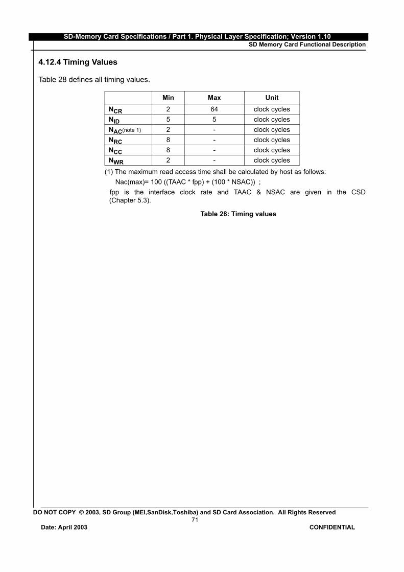
DO NOT COPY © 2003, SD Group (MEI,SanDisk,Toshiba) and SD Card Association. All Rights Reserved 71 hh
Date: April 2003 CONFIDENTIAL
SD-Memory Card Specifications / Part 1. Physical Layer Specification; Version 1.10 SD Memory Card Functional Description
4.12.4 Timing Values
Table 28 defines all timing values.
Min Max UnitNCR 2 64 clock cyclesNID 5 5 clock cyclesNAC(note 1) 2 - clock cyclesNRC 8 - clock cyclesNCC 8 - clock cyclesNWR 2 - clock cycles
(1) The maximum read access time shall be calculated by host as follows:Nac(max)= 100 ((TAAC * fpp) + (100 * NSAC)) ;
fpp is the interface clock rate and TAAC & NSAC are given in the CSD(Chapter 5.3).
Table 28: Timing values

DO NOT COPY © 2003, SD Group (MEI,SanDisk,Toshiba) and SD Card Association. All Rights Reserved 72 hh
Date: April 2003 CONFIDENTIAL
SD-Memory Card Specifications / Part 1. Physical Layer Specification; Version 1.10 Card Registers
5 Card Registers
Within the card interface six registers are defined: OCR, CID, CSD, RCA, DSR and SCR. These canbe accessed only by corresponding commands (see Chapter 4.7). The OCR, CID, CSD and SCRregisters carry the card/content specific information, while the RCA and DSR registers are configu-ration registers storing actual configuration parameters.
5.1 OCR RegisterThe 32-bit operation conditions register stores the VDD voltage profile of the card. In addition, thisregister includes a status information bit. This status bit is set if the card power up procedure hasbeen finished. The OCR register shall be implemented by the cards which do not support the fulloperating voltage range of the SD Memory Card bus, or if the card power up extends the definitionin the timing diagram (Figure 38).
OCR bit position VDD voltage window0-3 reserved4 reserved 5 reserved6 reserved7 reserved8 2.0-2.19 2.1-2.210 2.2-2.311 2.3-2.412 2.4-2.513 2.5-2.614 2.6-2.715 2.7-2.816 2.8-2.917 2.9-3.018 3.0-3.119 3.1-3.220 3.2-3.321 3.3-3.422 3.4-3.523 3.5-3.624-30 reserved31 card power up status bit (busy)1
1)This bit is set to LOW if the card has not finished the power up routine Table 29: OCR register definition

DO NOT COPY © 2003, SD Group (MEI,SanDisk,Toshiba) and SD Card Association. All Rights Reserved 73 hh
Date: April 2003 CONFIDENTIAL
SD-Memory Card Specifications / Part 1. Physical Layer Specification; Version 1.10 Card Registers
The supported voltage range is coded as shown in Table 29. A voltage range is not supported if thecorresponding bit value is set to LOW. As long as the card is busy, the corresponding bit (31) is setto LOW.
5.2 CID RegisterThe Card IDentification (CID) register is 128 bits wide. It contains the card identification informationused during the card identification phase. Every individual flash card shall have a unique identifica-tion number. The structure of the CID register is defined in the following paragraphs:
• MIDAn 8 bit binary number that identifies the card manufacturer. The MID number is controlled, definedand allocated to a SD Memory Card manufacturer by the SD Group. This procedure is establishedto ensure uniqueness of the CID register.
• OIDA 2 ASCII string characters that identifies the card OEM and/or the card contents (when used as adistribution media either on ROM or FLASH cards). The OID number is controlled, defined and allo-cated to a SD Memory Card manufacturer by the SD Group. This procedure is established toensure uniqueness of the CID register.
• PNMThe product name is a string, 5 ASCII characters long.
• PRVThe product revision is composed of two Binary Coded Decimal (BCD) digits, four bits each, repre-senting an “n.m” revision number. The “n” is the most significant nibble and “m” is the least signifi-cant nibble. As an example, the PRV binary value field for product revision “6.2” will be: 0110 0010
Name Field Width CID-sliceManufacturer ID MID 8 [127:120]OEM/Application ID OID 16 [119:104]Product name PNM 40 [103:64]Product revision PRV 8 [63:56]Product serial number PSN 32 [55:24]reserved -- 4 [23:20]Manufacturing date MDT 12 [19:8]CRC7 checksum CRC 7 [7:1]not used, always ’1’ - 1 [0:0]
Table 30: The CID fields

DO NOT COPY © 2003, SD Group (MEI,SanDisk,Toshiba) and SD Card Association. All Rights Reserved 74 hh
Date: April 2003 CONFIDENTIAL
SD-Memory Card Specifications / Part 1. Physical Layer Specification; Version 1.10 Card Registers
• PSNThe Serial Number is 32 bits of binary number.
• MDTThe manufacturing date composed of two hexadecimal digits, one is 8 bit representing the year(y)and the other is four bits representing the month(m).The “m” field [11:8] is the month code. 1 = January.The “y” field [19:12] is the year code. 0 = 2000.As an example, the binary value of the Date field for production date “April 2001” will be: 00000001 0100.
• CRCCRC7 checksum (7 bits). This is the checksum of the CID contents computed according to Chapter4.5.
5.3 CSD Register
The Card-Specific Data register provides information on how to access the card contents. The CSDdefines the data format, error correction type, maximum data access time, whether the DSR registercan be used etc. The programmable part of the register (entries marked by W or E, see below) can bechanged by CMD27. The type of the entries in the table below is coded as follows: R = readable,W(1) = writable once, W = multiple writable.
Name Field Width CellType CSD-slice
CSD structure CSD_STRUCTURE 2 R [127:126]reserved - 6 R [125:120]data read access-time-1 TAAC 8 R [119:112]data read access-time-2 in CLK cycles (NSAC*100)
NSAC 8 R [111:104]
max. data transfer rate TRAN_SPEED 8 R [103:96]card command classes CCC 12 R [95:84]max. read data block length READ_BL_LEN 4 R [83:80]partial blocks for read allowed READ_BL_PARTIAL 1 R [79:79]write block misalignment WRITE_BLK_MISALIGN 1 R [78:78]read block misalignment READ_BLK_MISALIGN 1 R [77:77]DSR implemented DSR_IMP 1 R [76:76]reserved - 2 R [75:74]device size C_SIZE 12 R [73:62]max. read current @VDD min VDD_R_CURR_MIN 3 R [61:59]
Table 31: The CSD Register fields

DO NOT COPY © 2003, SD Group (MEI,SanDisk,Toshiba) and SD Card Association. All Rights Reserved 75 hh
Date: April 2003 CONFIDENTIAL
SD-Memory Card Specifications / Part 1. Physical Layer Specification; Version 1.10 Card Registers
The following sections describe the CSD fields and the relevant data types. If not explicitly definedotherwise, all bit strings are interpreted as binary coded numbers starting with the left bit first.
• CSD_STRUCTUREVersion number of the related CSD structure.
max. read current @VDD max VDD_R_CURR_MAX 3 R [58:56]max. write current @VDD min VDD_W_CURR_MIN 3 R [55:53]max. write current @VDD max VDD_W_CURR_MAX 3 R [52:50]device size multiplier C_SIZE_MULT 3 R [49:47]erase single block enable ERASE_BLK_EN 1 R [46:46]erase sector size SECTOR_SIZE 7 R [45:39]write protect group size WP_GRP_SIZE 7 R [38:32]write protect group enable WP_GRP_ENABLE 1 R [31:31]reserved for MultiMediaCard compatibility 2 R [30:29]write speed factor R2W_FACTOR 3 R [28:26]max. write data block length WRITE_BL_LEN 4 R [25:22]partial blocks for write allowed WRITE_BL_PARTIAL 1 R [21:21]reserved - 5 R [20:16]File format group FILE_FORMAT_GRP 1 R/W(1) [15:15]copy flag (OTP) COPY 1 R/W(1) [14:14]permanent write protection PERM_WRITE_PROTECT 1 R/W(1) [13:13]temporary write protection TMP_WRITE_PROTECT 1 R/W [12:12]File format FILE_FORMAT 2 R/W(1) [11:10]reserved 2 R/W [9:8]CRC CRC 7 R/W [7:1]not used, always’1’ - 1 - [0:0]
CSD_STRUCTURE CSD structure version Valid for SD Memory Card Physical Specification Version
0 CSD version No. 1.0 Version 1.0-1.11-3 reserved
Table 32: CSD register structure
Name Field Width CellType CSD-slice
Table 31: The CSD Register fields

DO NOT COPY © 2003, SD Group (MEI,SanDisk,Toshiba) and SD Card Association. All Rights Reserved 76 hh
Date: April 2003 CONFIDENTIAL
SD-Memory Card Specifications / Part 1. Physical Layer Specification; Version 1.10 Card Registers
• TAACDefines the asynchronous part of the data access time.
• NSACDefines the worst case for the clock dependent factor of the data access time. The unit for NSAC is100 clock cycles. Therefore, the maximal value for the clock dependent part of the data access timeis 25.5k clock cycles. The total access time NAC as expressed in the Table 28 is the sum of TAAC and NSAC. It has to becomputed by the host for the actual clock rate. The read access time should be interpreted as a typ-ical delay for the first data bit of a data block or stream.
• TRAN_SPEEDThe following table defines the maximum data transfer rate per one data line - TRAN_SPEED:
Note that for current SD Memory Cards that field must be always 0_0110_010b (032h) which isequal to 25MHz - the mandatory maximum operating frequency of SD Memory Card.In High-Speed mode, that field must be always 0_1011_010b (05Ah) which is equal to 50MHz. Andwhen the timing mode returns to the default by CMD6 or CMD0 command, its value will be 032h.
• CCCThe SD Memory Card command set is divided into subsets (command classes). The card commandclass register CCC defines which command classes are supported by this card. A value of ‘1’ in a
TAAC bit position code
2:0 time unit0=1ns, 1=10ns, 2=100ns, 3=1µs, 4=10µs, 5=100µs, 6=1ms, 7=10ms
6:3 time value0=reserved, 1=1.0, 2=1.2, 3=1.3, 4=1.5, 5=2.0, 6=2.5, 7=3.0, 8=3.5, 9=4.0, A=4.5, B=5.0, C=5.5, D=6.0, E=7.0, F=8.0
7 reserved
Table 33: TAAC access time definition
TRAN_SPEED bit code2:0 transfer rate unit
0=100kbit/s, 1=1Mbit/s, 2=10Mbit/s, 3=100Mbit/s, 4... 7=reserved
6:3 time value0=reserved, 1=1.0, 2=1.2, 3=1.3, 4=1.5, 5=2.0, 6=2.5, 7=3.0, 8=3.5, 9=4.0, A=4.5, B=5.0, C=5.5, D=6.0, E=7.0, F=8.0
7 reserved
Table 34: Maximum data transfer rate definition

DO NOT COPY © 2003, SD Group (MEI,SanDisk,Toshiba) and SD Card Association. All Rights Reserved 77 hh
Date: April 2003 CONFIDENTIAL
SD-Memory Card Specifications / Part 1. Physical Layer Specification; Version 1.10 Card Registers
CCC bit means that the corresponding command class is supported. For command class definitionrefer to Table 8.
• READ_BL_LENThe maximum read data block length is computed as 2READ_BL_LEN. The maximum block lengthmight therefore be in the range 512...2048 bytes (see Chapter 4.11 for details). Note that in SDMemory Card the WRITE_BL_LEN is always equal to READ_BL_LEN
• READ_BL_PARTIAL (always = 1 in SD Memory Card) Partial Block Read is always allowed in SD Memory Card. It means that smaller blocks can be usedas well. The minimum block size will be one byte.
• WRITE_BLK_MISALIGNDefines if the data block to be written by one command can be spread over more than one physicalblock of the memory device. The size of the memory block is defined in WRITE_BL_LEN.WRITE_BLK_MISALIGN=0 signals that crossing physical block boundaries is invalid.WRITE_BLK_MISALIGN=1 signals that crossing physical block boundaries is allowed.
• READ_BLK_MISALIGNDefines if the data block to be read by one command can be spread over more than one physicalblock of the memory device. The size of the memory block is defined in READ_BL_LEN.READ_BLK_MISALIGN=0 signals that crossing physical block boundaries is invalid.READ_BLK_MISALIGN=1 signals that crossing physical block boundaries is allowed.
CCC bit Supported card command class0 class 01 class 1......11 class 11
Table 35: Supported card command classes
READ_BL_LEN Block length Remark0-8 reserved 9 29 = 512 Bytes ...... 11 211 = 2048 Bytes 12-15 reserved
Table 36: Data block length
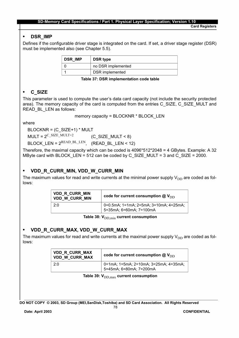
DO NOT COPY © 2003, SD Group (MEI,SanDisk,Toshiba) and SD Card Association. All Rights Reserved 78 hh
Date: April 2003 CONFIDENTIAL
SD-Memory Card Specifications / Part 1. Physical Layer Specification; Version 1.10 Card Registers
• DSR_IMPDefines if the configurable driver stage is integrated on the card. If set, a driver stage register (DSR)must be implemented also (see Chapter 5.5).
• C_SIZEThis parameter is used to compute the user’s data card capacity (not include the security protectedarea). The memory capacity of the card is computed from the entries C_SIZE, C_SIZE_MULT andREAD_BL_LEN as follows:
memory capacity = BLOCKNR * BLOCK_LENwhere
BLOCKNR = (C_SIZE+1) * MULTMULT = 2C_SIZE_MULT+2 (C_SIZE_MULT < 8)BLOCK_LEN = 2READ_BL_LEN, (READ_BL_LEN < 12)
Therefore, the maximal capacity which can be coded is 4096*512*2048 = 4 GBytes. Example: A 32MByte card with BLOCK_LEN = 512 can be coded by C_SIZE_MULT = 3 and C_SIZE = 2000.
• VDD_R_CURR_MIN, VDD_W_CURR_MINThe maximum values for read and write currents at the minimal power supply VDD are coded as fol-lows:
• VDD_R_CURR_MAX, VDD_W_CURR_MAXThe maximum values for read and write currents at the maximal power supply VDD are coded as fol-lows:
DSR_IMP DSR type0 no DSR implemented1 DSR implemented
Table 37: DSR implementation code table
VDD_R_CURR_MINVDD_W_CURR_MIN code for current consumption @ VDD
2:0 0=0.5mA; 1=1mA; 2=5mA; 3=10mA; 4=25mA; 5=35mA; 6=60mA; 7=100mA
Table 38: VDD,min current consumption
VDD_R_CURR_MAXVDD_W_CURR_MAX code for current consumption @ VDD
2:0 0=1mA; 1=5mA; 2=10mA; 3=25mA; 4=35mA; 5=45mA; 6=80mA; 7=200mA
Table 39: VDD,max current consumption

DO NOT COPY © 2003, SD Group (MEI,SanDisk,Toshiba) and SD Card Association. All Rights Reserved 79 hh
Date: April 2003 CONFIDENTIAL
SD-Memory Card Specifications / Part 1. Physical Layer Specification; Version 1.10 Card Registers
• C_SIZE_MULTThis parameter is used for coding a factor MULT for computing the total device size (see ‘C_SIZE’).The factor MULT is defined as 2C_SIZE_MULT+2.
• ERASE_BLK_ENDefines whether erase of one write block (see WRITE_BL_LEN) is allowed (beside theSECTOR_SIZE given bellow). If ERASE_BLK_EN = ’0’ erase area is unit of SECTOR_SIZE.if ERASE_BLK_EN = ’1’ erase area is unit of SECTOR_SIZE or unit of WRITE_BL_LEN.
• SECTOR_SIZEThe size of an erasable sector. The contents of this register is a 7 bit binary coded value, definingthe number of write blocks (see WRITE_BL_LEN). The actual size is computed by increasing thisnumber by one. A value of zero means 1 write block, 127 means 128 write blocks.
• WP_GRP_SIZEThe size of a write protected group. The contents of this register is a 7 bit binary coded value, defin-ing the number of erase sectors (see SECTOR_SIZE). The actual size is computed by increasingthis number by one. A value of zero means 1 erase sector, 127 means 128 erase sectors.
• WP_GRP_ENABLEA value of ‘0’ means no group write protection possible.
• R2W_FACTORDefines the typical block program time as a multiple of the read access time. The following table
C_SIZE_MULT MULT Remark0 22 = 41 23 = 82 24 = 163 25 = 324 26 = 64 5 27 = 1286 28 = 2567 29 = 512
Table 40: Multiply factor for the device size
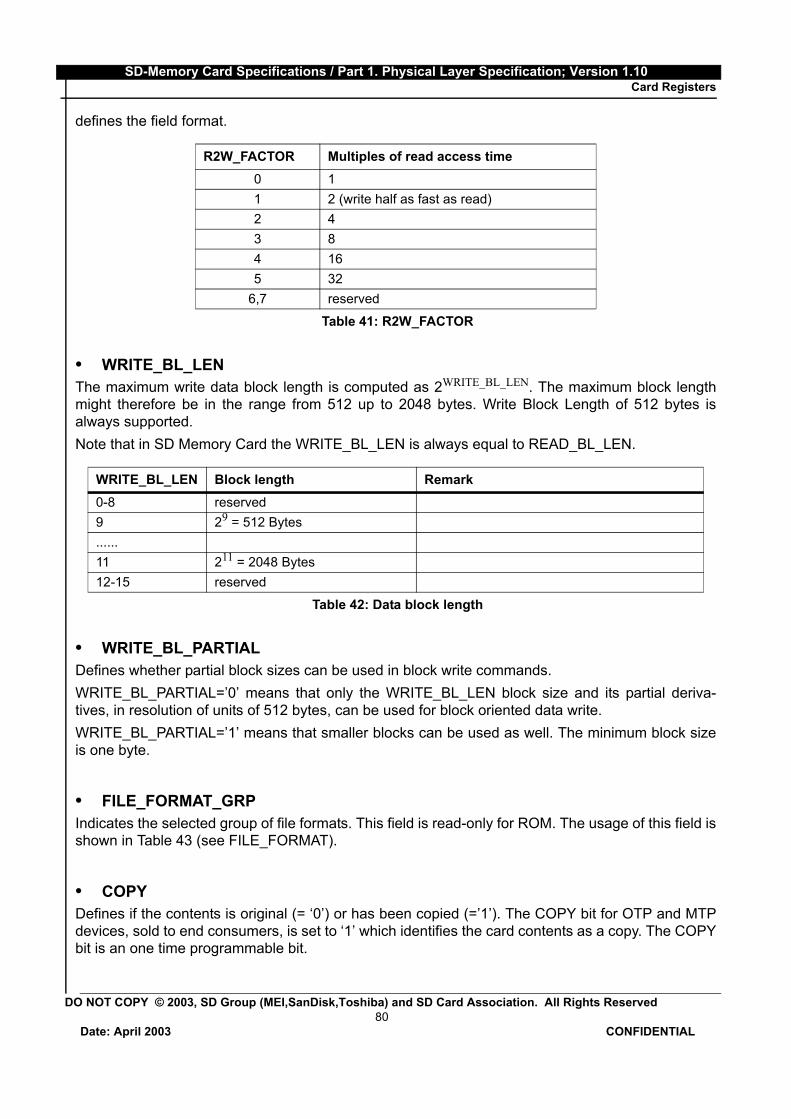
DO NOT COPY © 2003, SD Group (MEI,SanDisk,Toshiba) and SD Card Association. All Rights Reserved 80 hh
Date: April 2003 CONFIDENTIAL
SD-Memory Card Specifications / Part 1. Physical Layer Specification; Version 1.10 Card Registers
defines the field format.
• WRITE_BL_LENThe maximum write data block length is computed as 2WRITE_BL_LEN. The maximum block lengthmight therefore be in the range from 512 up to 2048 bytes. Write Block Length of 512 bytes isalways supported. Note that in SD Memory Card the WRITE_BL_LEN is always equal to READ_BL_LEN.
• WRITE_BL_PARTIALDefines whether partial block sizes can be used in block write commands. WRITE_BL_PARTIAL=’0’ means that only the WRITE_BL_LEN block size and its partial deriva-tives, in resolution of units of 512 bytes, can be used for block oriented data write.WRITE_BL_PARTIAL=’1’ means that smaller blocks can be used as well. The minimum block sizeis one byte.
• FILE_FORMAT_GRPIndicates the selected group of file formats. This field is read-only for ROM. The usage of this field isshown in Table 43 (see FILE_FORMAT).
• COPYDefines if the contents is original (= ‘0’) or has been copied (=’1’). The COPY bit for OTP and MTPdevices, sold to end consumers, is set to ‘1’ which identifies the card contents as a copy. The COPYbit is an one time programmable bit.
R2W_FACTOR Multiples of read access time0 11 2 (write half as fast as read)2 43 84 165 32
6,7 reserved
Table 41: R2W_FACTOR
WRITE_BL_LEN Block length Remark0-8 reserved9 29 = 512 Bytes......11 211 = 2048 Bytes12-15 reserved
Table 42: Data block length
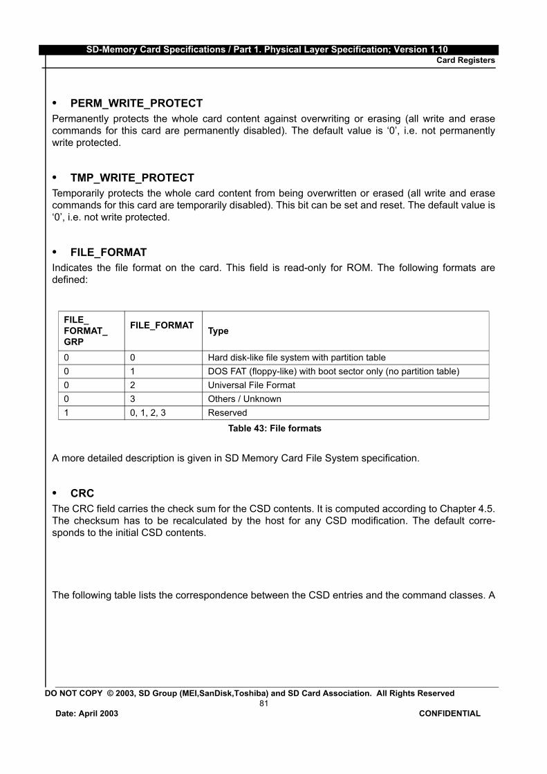
DO NOT COPY © 2003, SD Group (MEI,SanDisk,Toshiba) and SD Card Association. All Rights Reserved 81 hh
Date: April 2003 CONFIDENTIAL
SD-Memory Card Specifications / Part 1. Physical Layer Specification; Version 1.10 Card Registers
• PERM_WRITE_PROTECTPermanently protects the whole card content against overwriting or erasing (all write and erasecommands for this card are permanently disabled). The default value is ‘0’, i.e. not permanentlywrite protected.
• TMP_WRITE_PROTECTTemporarily protects the whole card content from being overwritten or erased (all write and erasecommands for this card are temporarily disabled). This bit can be set and reset. The default value is‘0’, i.e. not write protected.
• FILE_FORMATIndicates the file format on the card. This field is read-only for ROM. The following formats aredefined:
A more detailed description is given in SD Memory Card File System specification.
• CRCThe CRC field carries the check sum for the CSD contents. It is computed according to Chapter 4.5.The checksum has to be recalculated by the host for any CSD modification. The default corre-sponds to the initial CSD contents.
The following table lists the correspondence between the CSD entries and the command classes. A
FILE_FORMAT_GRP
FILE_FORMAT Type
0 0 Hard disk-like file system with partition table0 1 DOS FAT (floppy-like) with boot sector only (no partition table)0 2 Universal File Format0 3 Others / Unknown1 0, 1, 2, 3 Reserved
Table 43: File formats
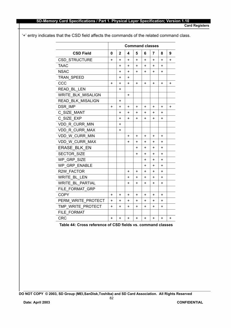
DO NOT COPY © 2003, SD Group (MEI,SanDisk,Toshiba) and SD Card Association. All Rights Reserved 82 hh
Date: April 2003 CONFIDENTIAL
SD-Memory Card Specifications / Part 1. Physical Layer Specification; Version 1.10 Card Registers
‘+’ entry indicates that the CSD field affects the commands of the related command class.
Command classes
CSD Field 0 2 4 5 6 7 8 9CSD_STRUCTURE + + + + + + + +TAAC + + + + + +NSAC + + + + + +TRAN_SPEED + +CCC + + + + + + + +READ_BL_LEN +WRITE_BLK_MISALIGN +READ_BLK_MISALIGN +DSR_IMP + + + + + + + +C_SIZE_MANT + + + + + +C_SIZE_EXP + + + + + +VDD_R_CURR_MIN +VDD_R_CURR_MAX +VDD_W_CURR_MIN + + + + +VDD_W_CURR_MAX + + + + +ERASE_BLK_EN + + + +SECTOR_SIZE + + + +WP_GRP_SIZE + + +WP_GRP_ENABLE + + +R2W_FACTOR + + + + +WRITE_BL_LEN + + + + +WRITE_BL_PARTIAL + + + + +FILE_FORMAT_GRPCOPY + + + + + + +PERM_WRITE_PROTECT + + + + + + +TMP_WRITE_PROTECT + + + + + + +FILE_FORMATCRC + + + + + + + +
Table 44: Cross reference of CSD fields vs. command classes

DO NOT COPY © 2003, SD Group (MEI,SanDisk,Toshiba) and SD Card Association. All Rights Reserved 83 hh
Date: April 2003 CONFIDENTIAL
SD-Memory Card Specifications / Part 1. Physical Layer Specification; Version 1.10 Card Registers
5.4 RCA Register
The writable 16-bit relative card address register carries the card address that is published by thecard during the card identification. This address is used for the addressed host-card communicationafter the card identification procedure. The default value of the RCA register is 0x0000. The value0x0000 is reserved to set all cards into the Stand-by State with CMD7.
5.5 DSR Register (Optional)
The 16-bit driver stage register is described in detail in Chapter 6.5. It can be optionally used toimprove the bus performance for extended operating conditions (depending on parameters like buslength, transfer rate or number of cards). The CSD register carries the information about the DSRregister usage. The default value of the DSR register is 0x404.
5.6 SCR RegisterIn addition to the CSD register there is another configuration register that named - SD CARD Con-figuration Register (SCR). SCR provides information on SD Memory Card's special features thatwere configured into the given card. The size of SCR register is 64 bit. This register shall be set inthe factory by the SD Memory Card manufacturer.The following table describes the SCR register content.
Table 45: The SCR Fields
• SCR_STRUCTUREVersion number of the related SCR structure in the SD Memory Card Physical Layer Specification.
• SD_SPECDescribes the SD Memory Card Physical Layer Specification version supported by this card.
Description Field Width CellType
SCRSlice
SCR Structure SCR_STRUCTURE 4 R [63:60]SD Memory Card - Spec. Version SD_SPEC 4 R [59:56]data_status_after erases DATA_STAT_AFTER_ERASE 1 R [55:55]SD Security Support SD_SECURITY 3 R [54:52]DAT Bus widths supported SD_BUS_WIDTHS 4 R [51:48]reserved - 16 R [47:32]reserved for manufacturer usage - 32 R [31:0]
SCR_STRUCTURE SCR structure version Valid for SD Physical Layer Specification Version
0 SCR version No. 1.0 Version 1.0-1.11-15 reserved
Table 46: SCR register structure version

DO NOT COPY © 2003, SD Group (MEI,SanDisk,Toshiba) and SD Card Association. All Rights Reserved 84 hh
Date: April 2003 CONFIDENTIAL
SD-Memory Card Specifications / Part 1. Physical Layer Specification; Version 1.10 Card Registers
• DATA_STAT_AFTER_ERASEDefines the data status after erase, whether it is ‘0’ or ‘1’ (the status is card vendor dependent).
• SD_SECURITYDescribes the security algorithm supported by the card.
Security Protocol 1.0 relates to Security Specification Version 0.96.Security Protocol 2.0 relates to Security Specification Version 1.0.-1.01Note that it is mandatory for a regular writable SD Memory Card to support Security Protocol. ForROM (Read Only) and OTP (One Time Programmable) type of SD Memory Card the security fea-ture is optional
• SD_BUS_WIDTHSDescribes all the DAT bus widths that are supported by this card.
Since SD Memory Card shall support at least the two bus modes 1bit or 4bit width then any SDCard shall set at least bits 0 and 2 (SD_BUS_WIDTH="0101").
SPEC_VERS Physical Layer Specification Version Number
0 Version 1.0-1.011 Version 1.12-15 reserved
Table 47: SD Memory Card Physical Layer Specification Version
SD_SECURITY Supported algorithm0 no security1 security protocol 1.02 security protocol 2.03 .. 7 reserved
Table 48: SD Supported security algorithm
SD_BUS_WIDTHS Supported Bus WidthsBit 0 1 bit (DAT0)Bit 1 reservedBit 2 4 bit (DAT0-3)Bit 3 [MSB] reserved
Table 49: SD Memory Card Supported Bus Widths

DO NOT COPY © 2003, SD Group (MEI,SanDisk,Toshiba) and SD Card Association. All Rights Reserved 85 hh
Date: April 2003 CONFIDENTIAL
SD-Memory Card Specifications / Part 1. Physical Layer Specification; Version 1.10 SD Memory Card Hardware Interface
6 SD Memory Card Hardware Interface
The SD Memory Card has six communication lines and three supply lines:• CMD: Command is a bidirectional signal. The host and card drivers are operating in push pull
mode.• DAT0-3: Data lines are bidirectional signals. Host and card drivers are operating in push pull
mode• CLK: Clock is a host to card signal. CLK operates in push pull mode• VDD: VDD is the power supply line for all cards.• VSS1, VSS2 are two ground lines.In addition to those lines that are connected to the internal card circuitry there are two contacts ofthe Write Protect/Card Detect switch that are part of the socket. Those contacts are not mandatorybut if they are exist they should be connected as given in the following figure.When DAT3 is used for card detection, RDAT for DAT3 should be unconnected and an another resis-tor should be connected to the ground.
Figure 35: Bus circuitry diagram
RDAT and RCMD are pull-up resistors protecting the CMD and the DAT lines against bus floatingwhen no card is inserted or when all card drivers are in an high-impedance mode.The host shall pull-up all DAT0-3 lines by RDAT, even if the host uses SD Memory Card as 1 bit-mode-only in SD mode. Also, the host shall pull-up all "RSV" lines in SPI mode, eventhough theyare not used.RWP is used for the Write Protect/Card Detection switch.Refer to Chapter 6.6 for components values and conditions.
6.1 Hot insertion and removal
To guarantee the proper sequence of card pin connection during hot insertion, the use of either a
CMD
CLK
DAT0-3SD
MemoryCardHost 1 2 3 4 5 6 7 8
SD Memory Card
RDAT RCMD
C1 C2 C3
9
RWP
VssWrite Protect

DO NOT COPY © 2003, SD Group (MEI,SanDisk,Toshiba) and SD Card Association. All Rights Reserved 86 hh
Date: April 2003 CONFIDENTIAL
SD-Memory Card Specifications / Part 1. Physical Layer Specification; Version 1.10 SD Memory Card Hardware Interface
special hot-insertion capable card connector or an auto-detect loop on the host side (or some simi-lar mechanism) is mandatory (see Chapter 7). No card shall be damaged by inserting or removing a card into the SD Memory Card bus even whenthe power (VDD) is up. Data transfer operations are protected by CRC codes, therefore any bitchanges induced by card insertion and removal can be detected by the SD Memory Card bus mas-ter. The inserted card must be properly reset also when CLK carries a clock frequency fPP. Each cardshall have power protection to prevent card (and host) damage. Data transfer failures induced byremoval/insertion are detected by the bus master. They must be corrected by the application, whichmay repeat the issued command.
6.2 Card Detection (Insertion/Removal)In order to be able to give feedback indication to the users, SD Memory Card system shall imple-ment detection of card insertion or removal. One method is by sensing pin 1 of the card, and detect-ing the pull-up resistance on it. Detailed description of this and several other card detection optionsis given in Application Note “Card Detection Implementations”. In any case since it is not guarantythat all the MultiMediaCards in the market support the proposed card detection methods in SDMemory Card then the SD Memory Card host shall not ignore non-detected cards (empty sockets).If the host gets command from the user to operate a card it shall try to initialize a card in the socketeven if no card insertion was previously reported - just in case that MultiMediaCards that do not sup-port the card detection method is inside the socket.
6.3 Power protection (Insertion/Removal)
Cards shall be inserted/removed into/from the bus without damage. If one of the supply pins (VDD orVSS) is not connected properly, then the current is drawn through a data line to supply the card.
Figure 36: Improper power supply
CardController
VDD
Vss
CMD, DAT,
VDD not connected
Vss not connectedCLK

DO NOT COPY © 2003, SD Group (MEI,SanDisk,Toshiba) and SD Card Association. All Rights Reserved 87 hh
Date: April 2003 CONFIDENTIAL
SD-Memory Card Specifications / Part 1. Physical Layer Specification; Version 1.10 SD Memory Card Hardware Interface
Every card’s output also shall be able to withstand shortcuts to either supply.
If hot insertion feature is implemented in the host, than the host has to withstand an instant shortcutbetween VDD and VSS without damage.
6.4 Power up
The power up of the SD Memory Card bus is handled locally in each SD Memory Card and in thebus master.
Figure 37: Short cut protection
VDD
Vss
CMD, DAT,CLK
i short
i short
wor
st c
ase
shor
tcut
Connector

DO NOT COPY © 2003, SD Group (MEI,SanDisk,Toshiba) and SD Card Association. All Rights Reserved 88 hh
Date: April 2003 CONFIDENTIAL
SD-Memory Card Specifications / Part 1. Physical Layer Specification; Version 1.10 SD Memory Card Hardware Interface
• After power up (including hot insertion, i.e. inserting a card when the bus is operating) the SDMemory Card enters the idle state. During this state the SD Memory Card ignores all bus trans-actions until ACMD41 is received (ACMD command type shall always precede with CMD55).
• ACMD41 is a special synchronization command used to negotiate the operation voltage rangeand to poll the cards until they are out of their power-up sequence. Besides the operation voltageprofile of the cards, the response to ACMD41 contains a busy flag, indicating that the card is stillworking on its power-up procedure and is not ready for identification. This bit informs the hostthat the card is not ready. The host has to wait (and continue to poll the cards, each one on histurn) until this bit is cleared. The maximum time period until Busy bit will be cleared is 1Sec.
• Getting individual cards, as well as the whole SD Memory Card system, out of idle state is up tothe responsibility of the bus master. Since the power up time and the supply ramp up timedepend on application parameters such as the maximum number of SD Memory Card s, the buslength and the power supply unit, the host must ensure that the power is built up to the operatinglevel (the same level which will be specified in ACMD41) before ACMD41 is transmitted.
• After power up the host starts the clock and sends the initializing sequence on the CMD line. Thissequence is a contiguous stream of logical ‘1’s. The sequence length is the maximum of 1msec,74 clocks or the supply-ramp-up-time; The additional 10 clocks (over the 64 clocks after what thecard should be ready for communication) is provided to eliminate power-up synchronizationproblems.
• Every bus master shall have the capability to implement ACMD41 and CMD1. CMD1 will be
Figure 38: Power-up diagram
Supply voltage
Supply ramp up time
Bus master supply voltage
ACMD
VDD max
Valid voltage range for commands CMD0, 15, 55 and ACMD41
Valid voltage range for all other com-mands and memory access
Power up time
Initialization delay: Optional repetitions of ACMD41
The maximum of
CMD2NCC
until no cards are respondingwith busy bit set.
NCC NCC
1 msec, 74 clock cyclesand supply ramp up time
Initialization sequence 41ACMD
41ACMD
41
VDD min
time
Time out value for initialization process = 1Sec

DO NOT COPY © 2003, SD Group (MEI,SanDisk,Toshiba) and SD Card Association. All Rights Reserved 89 hh
Date: April 2003 CONFIDENTIAL
SD-Memory Card Specifications / Part 1. Physical Layer Specification; Version 1.10 SD Memory Card Hardware Interface
used to ask MultiMediaCards to send their Operation Conditions. In any case the ACMD41 or theCMD1 shall be send separately to each card accessing it through its own CMD line.
6.5 Programmable card output driver (Optional)
The bus capacitance of each line of the SD Memory Card bus is the sum of the bus master capaci-tance, the bus capacitance itself and the capacitance of each inserted card. The sum of host andbus capacitance are fixed for one application, but may vary between different applications.The cardload may vary in one application with each of the inserted cards.In the following, programmable card output drivers for the push pull mode are described as anoptional method for ensuring the defined maximum clock rate independently of the topology and ofthe number of inserted cards.Both data and command driver stages in the push-pull mode have programmable peak current driv-ing capabilities and programmable rise and fall times. The driver stage register (DSR) consists oftwo 8-bit latches. The contents of the latches is calculated from the required transfer speed of theinterface and the bus load. The CMD and DAT bus drivers consist of a predriver stage and a complementary driver transistor(Figure 39). The predriver stage output rise and fall time is set with the DSR1 register and deter-mines the speed of the driver stage. The complementary driver transistor size is set with the DSR2register and determines the current driving capabilities of the driver stage and also influences thepeak current consumption of the bus driver. The proper combination of both allows the optimum busperformance.Table 50 defines the DSR register contents:
The time in DSR1 specifies the switch-on time of the output driver transistors. At the external inter-face, it is measurable as a delay time between the clock and driver stage output signal (e.g. for test-ing).
DSR1 7 6 5 4 3 2 1 0tswitch-on max reserved 5ns 20ns 100ns 500nstswitch-on min 2ns 10ns 50ns 200ns
DSR2 7 6 5 4 3 2 1 0ipeak min
reserved100mA 20mA 5mA 1mA
ipeak max 200mA 50mA 10mA 2mAtrise typ 5ns 20ns 100ns 500ns
Table 50: DSR register contents

DO NOT COPY © 2003, SD Group (MEI,SanDisk,Toshiba) and SD Card Association. All Rights Reserved 90 hh
Date: April 2003 CONFIDENTIAL
SD-Memory Card Specifications / Part 1. Physical Layer Specification; Version 1.10 SD Memory Card Hardware Interface
Figure 39: SD Memory Card bus driver
All data is valid for the specified operating range (voltage, temperature). Any combination of DSR1and DSR2 bits may be programmed. DSR1 has to be programmed for the required clock frequency,where
fclock = (2 tswitch-on max)-1.The DSR2 register must be programmed with the required driver size. Hints for the proper driverstage selection are part of future application notes (see Appendix).
DAT0-3 out
CMD line in
CMD line out
Drive CMD pin
Drive DAT0-3 pin
Internal card clockCLK
DAT0-3
CMD
Driver StageRegister
pad
pad
pad
DAT0-3 line in
4
4
4
4

DO NOT COPY © 2003, SD Group (MEI,SanDisk,Toshiba) and SD Card Association. All Rights Reserved 91 hh
Date: April 2003 CONFIDENTIAL
SD-Memory Card Specifications / Part 1. Physical Layer Specification; Version 1.10 SD Memory Card Hardware Interface
6.6 Bus operating conditions
• General
Table 51: Bus Operating Cond. - General
• Power supply voltage
Table 52: Bus Operating Cond. - Power Supply Voltage
The current consumption of any card during the power-up period until the first command occuremust not exceed 15 mA averaged over 1 Second. From first command until ’stby_state’ (the statethat the host may read CSD and verify the operating current consumptions) the maximum currentconsumtion may be 100mA averaged over 1 Sec. Note that a card that is delivered before fixingPhysical Spec Ver 1.01, may not meet the above initialization current restrictions.
• Bus signal line loadThe total capacitance CL the CLK line of the SD Memory Card bus is the sum of the bus mastercapacitance CHOST, the bus capacitance CBUS itself and the capacitance CCARD of each card con-nected to this line:
CL = CHOST + CBUS + N CCARDwhere N is the number of connected cards. Requiring the sum of the host and bus capacitances notto exceed 30 pF for up to 10 cards, and 40 pF for up to 30 cards, the following values must not be
Parameter Symbol Min Max. Unit RemarkPeak voltage on all lines -0.3 VDD+0.3 V
All InputsInput Leakage Current -10 10 A
All OutputsOutput Leakage Current -10 10 A
Parameter Symbol Min Max. Unit Remark
Supply voltage VDD 2.0 3.6 VCMD0, 15, 55, ACMD41 commands
Supply voltage specified in OCR register
Except CMD0, 15, 55, ACMD41 commands
Supply voltage differentials (VSS1, VSS2) -0.3 0.3 V
Power up time 250 mS from 0v to VDD Min.

DO NOT COPY © 2003, SD Group (MEI,SanDisk,Toshiba) and SD Card Association. All Rights Reserved 92 hh
Date: April 2003 CONFIDENTIAL
SD-Memory Card Specifications / Part 1. Physical Layer Specification; Version 1.10 SD Memory Card Hardware Interface
exceeded:
Table 53: Bus Operating Cond. - Signal Line’s Load
Note that the total capacitance of CMD and DAT lines will be consist of CHOST, CBUS and oneCCARD only since they are connected separately to the SD Memory Card host.
6.7 Bus signal levelsAs the bus can be supplied with a variable supply voltage, all signal levels are related to the supplyvoltage.
Figure 40: Bus signal levels
To meet the requirements of the JEDEC specification JESD8-1A, the card input and output voltages
Parameter Symbol Min Max. Unit RemarkPull-up resistance RCMD
RDAT
10 100 k to prevent bus floating
Bus signal line capacitance CL 250 pF fPP 5 MHz, 21 cards
Bus signal line capacitance CL 100 pF fPP 20 MHz,7 cards
Single card capacitance CCARD 10 pFMaximum signal line inductance 16 nH fPP 20 MHzPull-up resistance inside card (pin1) RDAT3 10 90 k May be used for
card detection
VDD
input
input
undefined
V
t
output
output
high level
low level
high level
low level
VOH
VIH
VIL
VOL
VSS

DO NOT COPY © 2003, SD Group (MEI,SanDisk,Toshiba) and SD Card Association. All Rights Reserved 93 hh
Date: April 2003 CONFIDENTIAL
SD-Memory Card Specifications / Part 1. Physical Layer Specification; Version 1.10 SD Memory Card Hardware Interface
shall be within the following specified ranges for any VDD of the allowed voltage range:
Table 54: Bus Signal Cond. - I/O Signal Voltages
6.8 Bus timing (Default)
Figure 41: Timing diagram data input/output referenced to clock (Default)
Parameter Symbol Min Max. Unit ConditionsOutput HIGH voltage VOH 0.75 VDD V IOH=-100 A
@VDD minOutput LOW voltage VOL 0.125 VDD V IOL=100 A
@VDD minInput HIGH voltage VIH 0.625 VDD VDD + 0.3 VInput LOW voltage VIL VSS-0.3 0.25 VDD V
Parameter Symbol Min Max. Unit Remark
Clock CLK (All values are referred to min (VIH) and max (VIL),
Clock frequency Data Transfer Mode fPP 0 25 MHz CL 100 pF(7 cards)
VIL
VIH
VIL
Clock
Input
Output
fPP
tWL tWH
tIH
tTHL tTLH
tODLY(max)
VOH
VOL
VIH
Shaded areas are not valid
tISU
0.7
0.2
tODLY(min)

DO NOT COPY © 2003, SD Group (MEI,SanDisk,Toshiba) and SD Card Association. All Rights Reserved 94 hh
Date: April 2003 CONFIDENTIAL
SD-Memory Card Specifications / Part 1. Physical Layer Specification; Version 1.10 SD Memory Card Hardware Interface
(1) 0Hz means to stop the clock. The given minimum frequency range is for cases were continues clock is required (refer toChapter 4.4 - Clock Control).
Table 55: Bus Timing - Parameters Values (Default)
6.9 Bus timing (High-speed Mode)
Clock frequency Identification Mode (the low freq. is required for MultiMediaCard compatibility).
fOD
0(1)/100KHz 400 kHz CL 250 pF
(21 cards)
Clock low time tWL 10 ns CL 100 pF(7 cards)
Clock high time tWH 10 ns CL 100 pF(7 cards)
Clock rise time tTLH 10 ns CL 100 pF(7 cards)
Clock fall time tTHL 10 ns CL 100 pF(7 cards)
Clock low time tWL 50 ns CL 250 pF(21 cards)
Clock high time tWH 50 ns CL 250 pF(21 cards)
Clock rise time tTLH 50 ns CL 250 pF(21 cards)
Clock fall time tTHL 50 ns CL 250 pF(21 cards)
Inputs CMD, DAT (referenced to CLK)
Input set-up time tISU 5 ns CL 25 pF(1 card)
Input hold time tIH 5 ns CL 25 pF(1 card)
Outputs CMD, DAT (referenced to CLK)
Output Delay time during Data Transfer Mode tODLY 0 14 ns CL 25 pF(1 card)
Output Delay time during Identification Mode tODLY 0 50 ns CL 25 pF(1 card)
Parameter Symbol Min Max. Unit Remark

DO NOT COPY © 2003, SD Group (MEI,SanDisk,Toshiba) and SD Card Association. All Rights Reserved 95 hh
Date: April 2003 CONFIDENTIAL
SD-Memory Card Specifications / Part 1. Physical Layer Specification; Version 1.10 SD Memory Card Hardware Interface
Figure 42: Timing diagram data input/output referenced to clock (High-Speed)
Parameter Symbol Min Max. Unit Remark
Clock CLK (All values are referred to min (VIH) and max (VIL),
Clock frequency Data Transfer Mode fPP 0 50 MHz
Clock low time tWL 7 ns
Clock high time tWH 7 ns
Clock rise time tTLH 3 ns
Clock fall time tTHL 3 ns
Inputs CMD, DAT (referenced to CLK)
Input set-up time tISU 6 ns
Input hold time tIH 2 ns
Outputs CMD, DAT (referenced to CLK)
Output Delay time during Data Transfer Mode tODLY 14 ns
Output Hold time tOH 2.5 ns
Total System capacitance for each line1 CL 40 pF
VIL
VIH
VIL
Clock
Input
Output
fPP
tWL tWH
tIH
tTHL tTLH
tODLY
VOH
VOL
VIH
Shaded areas are not valid
tISU
0.7
0.2
tOH
50%VDD

DO NOT COPY © 2003, SD Group (MEI,SanDisk,Toshiba) and SD Card Association. All Rights Reserved 96 hh
Date: April 2003 CONFIDENTIAL
SD-Memory Card Specifications / Part 1. Physical Layer Specification; Version 1.10 SD Memory Card Hardware Interface
Table 56: Bus Timing - Parameters Values (High-Speed)
6.10 SDLV Memory Card - Low Voltage SD Memory Cards
Next generation of SD Memory Cards will support operation at lower supply voltage.
Table 57: SDLV Memory Card - Power Supply Voltage
The SDLV Memory Cards (low voltage cards) will support identification and operation voltagebetween 1.6V up to 3.6v. That means that the host may operate between 1.6 and 3.6 volts. Thoughit is strongly recommended that the host will be developed in such a way that the initialization will bedone in the range of 2.0-3.6 volt. That will allow to communicate with regular SD Memory Cards atleast for the initialization process and then to put them in inactive state in case that the host wouldprefer to work in a lower voltage range of SDLV Memory Card rather than SD Memory Card.
Although not mechanically different, new and old cards will not necessarily be interchangeable in agiven system. The system definition allows an attempt to use old (high voltage) cards with new (lowvoltage) hosts. In case that the host supports initialization in the range of 2-3.6v the user will beinformed that this is a wrong type of card. In order to minimize customer dissatisfaction the SDLV Memory Cards will be labeled in such a waythat the user will be able to distinguish between SDLV Memory Cards and regular SD MemoryCards (2.0-3.6v operation).The marking method is to be defined [T.B.D].SDLV will be re-defined in Spec2.0, so it is highly recommended not to use.
1)In order to satisfy severe timing, host shall drive only one card.
Parameter Symbol Min Max. Unit Remark
SDLV Memory Card Supply voltage VDD 1.6 3.6 V
for Identification and regular operation
Supply voltage differentials (VSS1, VSS2) -0.2 0.2 V
Power up time 250 mS from 0v to VDD Min.

DO NOT COPY © 2003, SD Group (MEI,SanDisk,Toshiba) and SD Card Association. All Rights Reserved 97 hh
Date: April 2003 CONFIDENTIAL
SD-Memory Card Specifications / Part 1. Physical Layer Specification; Version 1.10 SD Memory Card mechanical specification
7 SD Memory Card mechanical specification
This chapter describes the mechanical and electromechanical features of the SD Memory Card,and furthermore the minimal recommendations to the SD Memory Card connector. All technicaldrafts follow DIN ISO standard.
The functions of the card package are:
- protecting the chip- easy handling for the end user- reliable electrical interconnection- reliable write protect/card detection capability- bearing textual information and image- appealing appearance
The functions of the connector are:
- attaching and fixing the card- electrical interconnecting the card to the system board- write protect/card detect indication- optional: switch on/off power supply- protection against card inverse insertion
7.1 Card package
Every card package shall have the characteristics described in the following sections.

DO NOT COPY © 2003, SD Group (MEI,SanDisk,Toshiba) and SD Card Association. All Rights Reserved 98 hh
Date: April 2003 CONFIDENTIAL
SD-Memory Card Specifications / Part 1. Physical Layer Specification; Version 1.10 SD Memory Card mechanical specification
7.1.1 Design and format
7.1.2 Reliability and durability
Dimensions SD Mem-ory Card package
24mm x 32mm; (min. 23.9mm x 31.9mm; max.24.1mm x 32.1mm)other dimensions Figure 43testing according to MIL STD 883, Meth 2016
thickness ’Inter Connect Area’: 2.1mm +/- 0.15mm or 1.4mm+/-0.15mm for Thin SD Card.’Substrate Area’: Max 2.25mm or Max 1.55 for Thin SD Card - see Figure 45.
label or printable area In ’Substrate Area’ only - see Figure 45.surface plain (except contact area)edges smooth edges, see Figure 44, Figure 45inverse insertion protection on left corner (top view) see Figure 47position of ESC contacts along middle of shorter edge see Figure 43 and Figure 44
Table 58: SD Memory Card Package - Dimensions
temperature operation: -25°C / 85°C (Target spec)storage: -40°C (168h) / 85°C (500h)junction temperature: max. 95°C
moisture and corrosion operation: 25°C / 95% rel. humiditystorage: 40°C / 93% rel. hum./500hsalt water spray:3% NaCl/35C; 24h acc. MIL STD Method 1009
durability 10.000 mating cycles; Test procedure: tbd.bending (note 1) 10Ntorque (note 1) 0.15N.m or +/-2.5 deg . drop test 1.5m free fallUV light exposure UV: 254nm, 15Ws/cm² according to ISO 7816-1visual inspectionshape and form (note 1)
no warpage; no mold skin; complete form; no cavities surface smoothness <= -0.1 mm/cm² within contour; no cracks; no pollution (fat, oil dust, etc.)
Minimum moving force of WP switch
40gf (Ensures that the WP switch will not slide while it isinserted to the connector).
WP Switch cycles minimum 1000 Cycles (@ Slide force 0.4N to 5N)Note (1): The SDA’s recommended test methods for Torque, bending and Warpage are defined in seperate Application Notes document.
Table 59: Reliability and Durability

DO NOT COPY © 2003, SD Group (MEI,SanDisk,Toshiba) and SD Card Association. All Rights Reserved 99 hh
Date: April 2003 CONFIDENTIAL
SD-Memory Card Specifications / Part 1. Physical Layer Specification; Version 1.10 SD Memory Card mechanical specification
7.1.3 Electrical Static Discharge (ESD) Requirements
ESD testing should be conducted according to IEC61000-4-2
Required ESD parameters are:
(1) Human body model +- 4 KV 100 pf / 1.5 Kohm(2) Machine model +- 0.25 KV 200 pf / 0 ohmContact Pads:
+/- 4kV, Human body model according to IEC61000-4-2
Non Contact Pads area:+/-8kV (coupling plane discharge)+/-15kV (air discharge)Human body model according to IEC61000-4-2
The SDA’s recommended test methods for the non-contact/air discharge tests are given in a separate Application Note document.
7.1.4 Quality assurance
The product traceability shall be ensured by an individual card identification number.

DO NOT COPY © 2003, SD Group (MEI,SanDisk,Toshiba) and SD Card Association. All Rights Reserved 100 hh
Date: April 2003 CONFIDENTIAL
SD-Memory Card Specifications / Part 1. Physical Layer Specification; Version 1.10 SD Memory Card mechanical specification
7.2 Mechanical form factor
The following 3 technical drawings define the card package of SD Memory Card with 2.1+/-0.15mmcard thickness (the Thin SD Memory Card drawings are given in Chapter 7.4 ).
Figure 43: SD Memory Card - Mechanical Description (1 out of 3)
Notes for all the mechanical descriptions of the SD Memory Card (including Thin SD Memory Card): Note 1) The numbers enclosed by a square means that it is the distance between base lines. Thosevalues are for information only (the given general tolerances are not related to them).Note 2) Pins #3 and #4 are located "0.2 Min." ahead of pins #1, #2, #5, #6, #7 and #8 . Note 3) This value "1.6 Max." is for pins #1, #2, #5, #6, #7, #8.
Note (3)
Note (2)

DO NOT COPY © 2003, SD Group (MEI,SanDisk,Toshiba) and SD Card Association. All Rights Reserved 101 hh
Date: April 2003 CONFIDENTIAL
SD-Memory Card Specifications / Part 1. Physical Layer Specification; Version 1.10 SD Memory Card mechanical specification
Figure 44: SD Memory Card - Mechanical Description (2 out of 3)

DO NOT COPY © 2003, SD Group (MEI,SanDisk,Toshiba) and SD Card Association. All Rights Reserved 102 hh
Date: April 2003 CONFIDENTIAL
SD-Memory Card Specifications / Part 1. Physical Layer Specification; Version 1.10 SD Memory Card mechanical specification
Figure 45: SD Memory Card - Mechanical Description (3 out of 3)
Figure 46 describes the Write Protect switch position at all various cases and card types.
Note: Refer to Table 62 for the definition of ’substrate’ and ’Inter Connect’ areas.
Inter ConnectArea
SubstrateArea

DO NOT COPY © 2003, SD Group (MEI,SanDisk,Toshiba) and SD Card Association. All Rights Reserved 103 hh
Date: April 2003 CONFIDENTIAL
SD-Memory Card Specifications / Part 1. Physical Layer Specification; Version 1.10 SD Memory Card mechanical specification
Figure 46: WP Switch definition for all cases and card types
7.3 System: card and connectorThe description of the connector is out of the scope of this document. However, minimal recommen-dations to the connector comprise the ability to guarantee Write Protect and Card Detection, hotinsertion and removal of the card, and to prevent inverse insertion.
7.3.1 Card hot insertion
To guarantee a reliable initialization during hot insertion, some measures shall be taken on the hostside. For instance, a special hot-insertion capable card connector may be used to guarantee theproper sequence of card pin connection. The card contacts are contacted in three steps:1) Ground Vss (pin 3) and supply voltage Vdd (pin 4).2) CLK, CMD, DAT0, DAT1, DAT2 and Vss (pin 6).3) CD / DAT3 (pin 1).Pins 3 and 4 should make first contact when inserting, and release last when extracting.As another method, a switch could ensure that the power is switched on only after all card pads arecontacted. Of course, any other similar mechanism is allowed.
7.3.2 Inverse insertion
Inverse insertion is prevented by the reclining corners of SD Memory Card and connector.
- R/W card(WP switch is movable)
- ROM card(WP area is fixed)
Write unable Write enable
This form is same as taking off the WP Switch from R/W card.
This is the case of 1.4mm card which does not support the WP switch.
Pulling downthe WP Switch.
Pulling up theWP Switch.
- R/W card(WP switch is movable)
- ROM card(WP area is fixed)
Write unable Write enable
This form is same as taking off the WP Switch from R/W card.
This is the case of 1.4mm card which does not support the WP switch.
Pulling downthe WP Switch.
Pulling up theWP Switch.

DO NOT COPY © 2003, SD Group (MEI,SanDisk,Toshiba) and SD Card Association. All Rights Reserved 104 hh
Date: April 2003 CONFIDENTIAL
SD-Memory Card Specifications / Part 1. Physical Layer Specification; Version 1.10 SD Memory Card mechanical specification
Figure 47: Inverse insertion
7.3.3 Card Orientation
For the benefit of unified terminology when discussing the three dimensional orientation of a card(e.g. for connector definition), the non contact-pads side (the side with the card label) is defined asthe TOP side of the card and the contact-pads side of the card is defined as the BOTTOM side ofthe card.
7.3.4 Write Protect Detection
In SD memory card the Write Protect switch is always mandatory for the card side. Note that forhosts that supports Read Only operations the Write Protect detection capability in the SD Connector(Host side) is not necessary.
7.4 Thin (1.4mm) SD Memory CardSD Memory cards with mechanical dimensions that will be suitable for extra small applications willbe available.The "Thin SD Memory card" has very similar form factor as the SD Memory Card that is given inChapter 7.2 above except it thickness. The thickness of the "Thin SD Memory Card" is 1.4mm+/-0.15mm.Figure 48, 65 and 61 are the mechanical drawings of Thin SD Memory Card.Note that even though the WP switch appears in the given diagram it was defined as an optional forThin SD Memory Card.
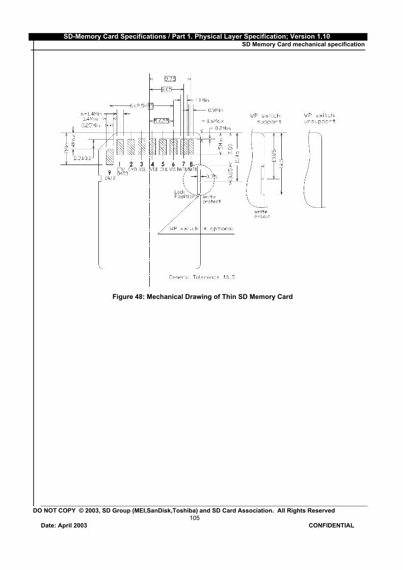
DO NOT COPY © 2003, SD Group (MEI,SanDisk,Toshiba) and SD Card Association. All Rights Reserved 105 hh
Date: April 2003 CONFIDENTIAL
SD-Memory Card Specifications / Part 1. Physical Layer Specification; Version 1.10 SD Memory Card mechanical specification
Figure 48: Mechanical Drawing of Thin SD Memory Card

DO NOT COPY © 2003, SD Group (MEI,SanDisk,Toshiba) and SD Card Association. All Rights Reserved 106 hh
Date: April 2003 CONFIDENTIAL
SD-Memory Card Specifications / Part 1. Physical Layer Specification; Version 1.10 SD Memory Card mechanical specification
Figure 49: Mechanical Drawing of Thin SD Memory Card

DO NOT COPY © 2003, SD Group (MEI,SanDisk,Toshiba) and SD Card Association. All Rights Reserved 107 hh
Date: April 2003 CONFIDENTIAL
SD-Memory Card Specifications / Part 1. Physical Layer Specification; Version 1.10 SPI Mode
8 SPI Mode
8.1 Introduction
The SPI mode consists of a secondary communication protocol which is offered by Flash-based SDMemory Cards. This mode is a subset of the SD Memory Card protocol, designed to communicatewith a SPI channel, commonly found in Motorola’s (and lately a few other vendors’) microcontrollers.The interface is selected during the first reset command after power up (CMD0) and cannot bechanged once the part is powered on. The SPI standard defines the physical link only, and not the complete data transfer protocol. The SDMemory Card SPI implementation uses a subset of the SD Memory Card protocol and commandset. The advantage of the SPI mode is the capability of using an off-the-shelf host, hence reducingthe design-in effort to minimum. The disadvantage is the loss of performance of the SPI mode ver-sus SD mode (e.g. Single data line and hardware CS signal per card).
8.2 SPI Bus ProtocolWhile the SD Memory Card channel is based on command and data bit streams which are initiatedby a start bit and terminated by a stop bit, the SPI channel is byte oriented. Every command or datablock is built of 8-bit bytes and is byte aligned to the CS signal (i.e. the length is a multiple of 8 clockcycles). Similar to the SD Memory Card protocol, the SPI messages consist of command, response anddata-block tokens. All communication between host and cards is controlled by the host (master).The host starts every bus transaction by asserting the CS signal low. The response behavior in the SPI mode differs from the SD mode in the following three aspects:• The selected card always responds to the command.• An additional (8 bit) response structure is used• When the card encounters a data retrieval problem, it will respond with an error response (which
replaces the expected data block) rather than by a time-out as in the SD mode.In addition to the command response, every data block sent to the card during write operations willbe responded with a special data response token. A data block may be as big as one card writeblock (WRITE_BL_LEN) and as small as a single byte. Partial block read/write operations areenabled by card options specified in the CSD register.

DO NOT COPY © 2003, SD Group (MEI,SanDisk,Toshiba) and SD Card Association. All Rights Reserved 108 hh
Date: April 2003 CONFIDENTIAL
SD-Memory Card Specifications / Part 1. Physical Layer Specification; Version 1.10 SPI Mode
Figure 50: SPI Mode Initialization Flow
8.2.1 Mode Selection
The SD Memory Card wakes up in the SD mode. It will enter SPI mode if the CS signal is asserted(negative) during the reception of the reset command (CMD0) and the card is in idle_state. If thecard recognizes that the SD mode is required it will not respond to the command and remain in theSD mode. If SPI mode is required the card will switch to SPI and respond with the SPI mode R1response.
The only way to return to the SD mode is by entering the power cycle. In SPI mode the SD MemoryCard protocol state machine is not observed. All the SD Memory Card commands supported in SPImode are always available. During the initialization sequence, if the host gets Illegal Command indication for ACMD41 sent tothe card, it may assume that the card is MultiMediaCard. In that case it should re-start the card asMultiMediaCard using CMD0 and CMD1.
8.2.2 Bus Transfer Protection
Every SD Memory Card token transferred on the bus is protected by CRC bits. In SPI mode, the SDMemory Card offers a non protected mode which enables systems built with reliable data links toexclude the hardware or firmware required for implementing the CRC generation and verificationfunctions.
ACMD41
Idle State(idle) CMD0
Power on
SPI OperationMode
CMD0 + CS Asserted (“0”)
SD Bus or MultiMedia Bus Operation Modes
from any stateexcept Inactive
card is busy ACMD41(*)
Start as MultiMediaCard
If Non valid CommandMust be a MultiMediaCard
using CMD0 and CMD1
data-transfer mode
card-identification mode
CMD58 (READ_OCR)
Not Mandatory to send CMD58:
Host shall refrain from
Though it is recommended
(*) Note: 2.1mm SD Memory Card can be initialized using CMD1 and Thin (1.4mm) SD Memory Card can be initialized using CMD1 only after
If the SD card is initialized by CMD1 and the host treat it as MMC card, not SD card, the Data of the card may be damaged because of
accessing this card
to be done in order to get thesupported voltage range ofthe card.
Case of non supported voltage range...
In SD Bus mode
CMD0
In SPI modefrom any state
firstly initialized by using CMD0 and ACMD 41. In any of the cases CMD1 is not recommended because it may be difficult for the host to distinguish between MultiMediaCard and SD Memory Card.
wrong interpretation of CSD and CID registers.

DO NOT COPY © 2003, SD Group (MEI,SanDisk,Toshiba) and SD Card Association. All Rights Reserved 109 hh
Date: April 2003 CONFIDENTIAL
SD-Memory Card Specifications / Part 1. Physical Layer Specification; Version 1.10 SPI Mode
In the non-protected mode the CRC bits of the command, response and data tokens are stillrequired in the tokens. However, they are defined as ‘don’t care’ for the transmitter and ignored bythe receiver.The SPI interface is initialized in the non-protected mode. However, the RESET command (CMD0)which is used to switch the card to SPI mode, is received by the card while in SD mode and, there-fore, must have a valid CRC field.Since CMD0 has no arguments, the content of all the fields, including the CRC field, are constantsand need not be calculated in run time. A valid reset command is:
0x40, 0x0, 0x0, 0x0, 0x0, 0x95The host can turn the CRC option on and off using the CRC_ON_OFF command (CMD59).
8.2.3 Data Read
The SPI mode supports single block read and Multiple Block read operations (CMD17 or CMD18 inthe SD Memory Card protocol). Upon reception of a valid read command the card will respond witha response token followed by a data token of the length defined in a previous SET_BLOCKLEN(CMD16) command (refer to Figure 51).
Figure 51: Single Block Read operation
A valid data block is suffixed with a 16 bit CRC generated by the standard CCITT polynomialx16+x12+x5+1.The maximum block length is given by READ_BL_LEN, defined in the CSD. If partial blocks areallowed (i.e. the CSD parameter READ_BL_PARTIAL equals 1), the block length can be any num-ber between 1 and the maximum block size. Otherwise, the only valid block length for data read isgiven by READ_BL_LEN.The start address can be any byte address in the valid address range of the card. Every block, how-ever, must be contained in a single physical card sector.In case of a data retrieval error, the card will not transmit any data. Instead, a special data errortoken will be sent to the host. Figure 52 shows a data read operation which terminated with an error
commandDataIn
DataOut
from host
to card
data from card to host
from card
to host
data blockresponse
command
NextCommand
CRC

DO NOT COPY © 2003, SD Group (MEI,SanDisk,Toshiba) and SD Card Association. All Rights Reserved 110 hh
Date: April 2003 CONFIDENTIAL
SD-Memory Card Specifications / Part 1. Physical Layer Specification; Version 1.10 SPI Mode
token rather than a data block.
Figure 52: Read operation - data error
In case of Multiple block read operation every transferred block has its suffixed of 16 bit CRC.Stop transmission command (CMD12) will actually stop the data transfer operation (the same as inSD Memory Card operation mode).
Figure 53: Multiple Block Read operation
8.2.4 Data Write
In SPI mode the SD Memory Card supports single block and Multiple block write commands. Uponreception of a valid write command (CMD24 or CMD25 in the SD Memory Card protocol), the cardwill respond with a response token and will wait for a data block to be sent from the host. CRC suf-fix, block length and start address restrictions are (with the exception of the CSD parameterWRITE_BL_PARTIAL controlling the partial block write option) identical to the read operation (seeFigure 54).
commandDataIn
DataOut
from host
to card
data error token from card to host
from card
to host
data errorresponse
command
NextCommand
commandDataIn
DataOut
from host
to card
data from card to host
from card
to host
data blockresponse
command
Stop Trans-mission
Command
CRC data block CRC
from card
to host
response

DO NOT COPY © 2003, SD Group (MEI,SanDisk,Toshiba) and SD Card Association. All Rights Reserved 111 hh
Date: April 2003 CONFIDENTIAL
SD-Memory Card Specifications / Part 1. Physical Layer Specification; Version 1.10 SPI Mode
Figure 54: Single Block Write operation
Every data block has a prefix of ’Start Block’ token (one byte).After a data block has been received, the card will respond with a data-response token. If the datablock has been received without errors, it will be programmed. As long as the card is busy program-ming, a continuous stream of busy tokens will be sent to the host (effectively holding the DataOutline low).Once the programming operation is completed, the host must check the results of the programmingusing the SEND_STATUS command (CMD13). Some errors (e.g. address out of range, write pro-tect violation etc.) are detected during programming only. The only validation check performed onthe data block and communicated to the host via the data-response token is the CRC and generalWrite Error indication. In Multiple Block write operation the stop transmission will be done by sending ’Stop Tran’ tokeninstead of ’Start Block’ token at the beginning of the next block. In case of Write Error indication (onthe data response) the host shall use SEND_NUM_WR_BLOCKS (ACMD22) in order to get thenumber of well written write blocks. The data tokens description is given in Chapter 8.3.3.
Figure 55: Multiple Block Write operation
While the card is busy, resetting the CS signal will not terminate the programming process. The cardwill release the DataOut line (tri-state) and continue with programming. If the card is reselectedbefore the programming is finished, the DataOut line will be forced back to low and all commandswill be rejected.Resetting a card (using CMD0) will terminate any pending or active programming operation. Thismay destroy the data formats on the card. It is in the responsibility of the host to prevent it.
data_response
command commandDataIn
DataOut
from host
to card
new command from host
data from host
to card
from card
to host
data block
busy
Dataresponse and
busy from card
response
Start BlockToken
data_response
command commandDataIn
DataOut
from host
to card
new command from host
data from host
to card
from card
to host
data block
busy
Dataresponse and
busy from card
response
Start Block Token
Stop Tran
Token
busy

DO NOT COPY © 2003, SD Group (MEI,SanDisk,Toshiba) and SD Card Association. All Rights Reserved 112 hh
Date: April 2003 CONFIDENTIAL
SD-Memory Card Specifications / Part 1. Physical Layer Specification; Version 1.10 SPI Mode
8.2.5 Erase & Write Protect Management
The erase and write protect management procedures in the SPI mode are identical to those of theSD mode. While the card is erasing or changing the write protection bits of the predefined sector list,it will be in a busy state and hold the DataOut line low. Figure 56 illustrates a ‘no data’ bus transac-tion with and without busy signalling.
Figure 56: ‘No data’ operations
8.2.6 Read CID/CSD Registers
Unlike the SD Memory Card protocol (where the register contents is sent as a command response),reading the contents of the CSD and CID registers in SPI mode is a simple read-block transaction.The card will respond with a standard response token (see Figure 52) followed by a data block of 16bytes suffixed with a 16 bit CRC.The data time out for the CSD command cannot be set to the cards TAAC since this value is storedin the card’s CSD. Therefore the standard response time-out value (NCR) is used for read latency ofthe CSD register.
8.2.7 Reset Sequence
The SD Memory Card requires a defined reset sequence. After power on reset or CMD0 (softwarereset) the card enters an idle state. At this state the only valid host commands are ACMD41(SD_SEND_OP_COND), CMD58 (READ_OCR) and CMD59 (CRC_ON_OFF). For the Thick(2.1mm) SD Memory Card - CMD1 (SEND_OP_COND) is also valid - that means that in SPI modeCMD1 and ACMD41 have the same behavior, though the usage of CMD41 is preferable since itallows easy distinguishing between SD Memory Card and MultiMediaCard. For the Thin (1.4mm)SD Memory Card CMD1 (SEND_OP_COND) is illegal command during the initialization that isdone after power on. After Power On, once the card accepted valid ACMD41, it will be able toaccept also CMD1 even if used after re-initializing (CMD0) the card. It was defined in such wayin order to be able to distinguish between Thin SD Memory Card and MultiMediaCards (that sup-ports CMD1 as well).The host must poll the card (by repeatedly sending CMD1 or ACMD41) until the ‘in-idle-state’ bit inthe card response indicates (by being set to 0) that the card completed its initialization processesand is ready for the next command.In SPI mode, as opposed to SD mode, ACMD41 (or CMD1 as well, for 2.1mm-SD Memory Card)has no operands and does not return the contents of the OCR register. Instead, the host may useCMD58 (available in SPI mode only) to read the OCR register. Furthermore, it is in the responsibility
command commandDataIn
DataOut
from host
to card
from host
to card
from card
to host
response response
from card
to host
busy

DO NOT COPY © 2003, SD Group (MEI,SanDisk,Toshiba) and SD Card Association. All Rights Reserved 113 hh
Date: April 2003 CONFIDENTIAL
SD-Memory Card Specifications / Part 1. Physical Layer Specification; Version 1.10 SPI Mode
of the host to refrain from accessing cards that do not support its voltage range.The usage of CMD58 is not restricted to the initializing phase only, but can be issued at any time.
8.2.8 Error Conditions
Unlike the SD Memory Card protocol, in the SPI mode the card will always respond to a command.The response indicates acceptance or rejection of the command. A command may be rejected inany one of the following cases: - It is sent while the card is in read operation (except CMD12 which is legal). - It is sent wile the card is in Busy. - Card is Locked and it is other than Class 0 or 7 commands. - It is not supported (illegal opcode). - CRC check failed.- It contains an illegal operand. - It was out of sequence during an erase sequence. Note that in case the host sends command while the card sends data in read operation then theresponse with an illegal command indication may disturb the data transfer.
8.2.9 Memory Array Partitioning
Same as for SD mode.
8.2.10 Card Lock/unlock
Usage of card lock and unlock commands in SPI mode is identical to SD mode. In both cases thecommand is responded with a R1b response type. After the busy signal clears, the host shouldobtain the result of the operation by issuing a GET_STATUS command. Refer to Chapter 4.3.6 fordetails.
8.2.11 Application Specific commands
Identical to SD mode with the exception of the APP_CMD status bit (refer to Chapter 4.10.1) whichis not available in SPI.
8.2.12 Copyright Protection commands
All the special Copyright Protection ACMDs and security functionality is the same as for SD mode.
8.2.13 Switch function command
Same as for SD mode with two exceptions:• The command is valid under the "not idle state".• In SPI mode, CMD0 switching period is within 8 clocks after the end bit of the CMD0 command
R1 response

DO NOT COPY © 2003, SD Group (MEI,SanDisk,Toshiba) and SD Card Association. All Rights Reserved 114 hh
Date: April 2003 CONFIDENTIAL
SD-Memory Card Specifications / Part 1. Physical Layer Specification; Version 1.10 SPI Mode
8.2.14 High-Speed mode (25MB/sec interface speed)
Same as for SD mode.
8.3 SPI Mode Transaction Packets
8.3.1 Command Tokens
• Command FormatAll the SD Memory Card commands are 6 bytes long. The command transmission always starts withthe left bit of the bitstring corresponding to the command codeword. All commands are protected bya CRC (see Chapter 4.5). The commands and arguments are listed in Table 62.
Table 60: Command Format
• Command ClassesAs in SD mode, the SPI commands are divided into several classes (See Table 61). Each class sup-ports a set of card functions. A SD Memory Card will support the same set of optional commandclasses in both communication modes (there is only one command class table in the CSD register).The available command classes, and the supported command for a specific class, however, are dif-ferent in the SD Memory Card and the SPI communication mode. Note that except the classes that are not supported in SPI mode (class 1, 3 and 9), the mandatoryrequired classes for the SD mode are the same for the SPI mode.
Bit position 47 46 [45:40] [39:8] [7:1] 0
Width (bits) 1 1 6 32 7 1
Value ‘0’ ‘1’ x x x ‘1’
Description start bit transmission bit
command index argument CRC7 end bit
CardCMDClass (CCC)
Class Description
Supported commands
0 1 6 9 10 12 13 16 17 18 24 25 27 28 29 30 32 33 34 35 36 37 38 42 50 52 53 55 56 57 58 59
class 0 Basic + + + + + + + +class 1 Not sup-
ported in SPIclass 2 Block read + + +class 3 Not sup-
ported in SPIclass 4 Block write + + + +class 5 Erase + + +
Table 61: Command classes in SPI mode

DO NOT COPY © 2003, SD Group (MEI,SanDisk,Toshiba) and SD Card Association. All Rights Reserved 115 hh
Date: April 2003 CONFIDENTIAL
SD-Memory Card Specifications / Part 1. Physical Layer Specification; Version 1.10 SPI Mode
• Detailed Command DescriptionThe following table provides a detailed description of the SPI bus commands. The responses aredefined in Chapter 8.3.2. The Table 62 lists all SD Memory Card commands. A “yes” in the SPImode colon indicates that the command is supported in SPI mode. With these restrictions, the com-mand class description in the CSD is still valid. If a command does not require an argument, thevalue of this field should be set to zero. The reserved commands are reserved in SD mode as well.The binary code of a command is defined by the mnemonic symbol. As an example, the content ofthe command index field is (binary) ‘000000’ for CMD0 and ‘100111’ for CMD39.
class 6 Write-protec-tion(Optional)
+ + +
class 7 Lock Card (Optional)
+ +
class 8 Application specific
+ +
class 9 I/O mode + +class 10 Switch + + + + + + +class 11 Reserved
CMDINDEX
SPIMode Argument Resp Abbreviation Command Description
CMD0 Yes None R1 GO_IDLE_STATE resets the SD Memory CardCMD1 Yes7 None R1 SEND_OP_
CONDActivates the card’s initialization pro-cess (In Thin- 1.4mm SD Memory Card it is valid only if used after re-ini-tializing a card - see note at Chapter 8.2.7)
CMD2 NoCMD3 NoCMD4 NoCMD5 reserved for I/O Mode (refer to "SDIO Card Specification")
Table 62: Commands and arguments
CardCMDClass (CCC)
Class Description
Supported commands
0 1 6 9 10 12 13 16 17 18 24 25 27 28 29 30 32 33 34 35 36 37 38 42 50 52 53 55 56 57 58 59
Table 61: Command classes in SPI mode

DO NOT COPY © 2003, SD Group (MEI,SanDisk,Toshiba) and SD Card Association. All Rights Reserved 116 hh
Date: April 2003 CONFIDENTIAL
SD-Memory Card Specifications / Part 1. Physical Layer Specification; Version 1.10 SPI Mode
CMD6 Yes [31] Mode 0:Check function 1:Switch function
[30:24] reserved (All ’0’)
[23:20] reserved for function group 6 (All ’0’ or 0xF)
[19:16] reserved for function group 5 (All ’0’ or 0xF)
[15:12] reserved for function group 4 (All ’0’ or 0xF)
[11:8] reserved for function group 3 (All ’0’ or 0xF)
[7:4] function group 2 for command system
[3:0] function group 1 for access mode
R1 SWITCH_FUNC Checks switchable function (mode 0) and switchs card function (mode 1).see Chapter 4.3.9.
CMD7 NoCMD8 reservedCMD9 Yes None R1 SEND_CSD asks the selected card to send its
card-specific data (CSD) CMD10 Yes None R1 SEND_CID asks the selected card to send its
card identification (CID)CMD11 NoCMD12 Yes Non R1b STOP_
TRANSMISSIONforces the card to stop transmission in Multiple Block Read Operation
CMD13 Yes None R2 SEND_STATUS asks the selected card to send its sta-tus register.
CMD14 reservedCMD15 No
CMDINDEX
SPIMode Argument Resp Abbreviation Command Description
Table 62: Commands and arguments

DO NOT COPY © 2003, SD Group (MEI,SanDisk,Toshiba) and SD Card Association. All Rights Reserved 117 hh
Date: April 2003 CONFIDENTIAL
SD-Memory Card Specifications / Part 1. Physical Layer Specification; Version 1.10 SPI Mode
CMD16 Yes [31:0] block length
R1 SET_BLOCKLEN selects a block length (in bytes) for all following block commands (read and write).1
CMD17 Yes [31:0] data address
R1 READ_SINGLE_BLOCK
reads a block of the size selected by the SET_BLOCKLEN command.2
CMD18 Yes [31:0] data address
R1 READ_MULTIPLE_BLOCK
continuously transfers data blocks from card to host until interrupted by a STOP_TRANSMISSION command.
CMD19 reservedCMD20 NoCMD21...CMD23
reserved
CMD24 Yes [31:0] data address
R1 WRITE_BLOCK writes a block of the size selected by the SET_BLOCKLEN command. 3
CMD25 Yes [31:0] data address
R1 WRITE_MULTIPLE_BLOCK
continuously writes blocks of data until ’Stop Tran’ token is sent (instead ’Start Block’).
CMD26 NoCMD27 Yes None R1 PROGRAM_CSD programming of the programmable
bits of the CSD.CMD28 Yes [31:0] data
addressR1b4 SET_WRITE_
PROTif the card has write protection fea-tures, this command sets the write protection bit of the addressed group. The properties of write protection are coded in the card specific data (WP_GRP_SIZE).
CMD29 Yes [31:0] data address
R1b CLR_WRITE_PROT
if the card has write protection fea-tures, this command clears the write protection bit of the addressed group.
CMD30 Yes [31:0] write protect data address
R1 SEND_WRITE_PROT
if the card has write protection fea-tures, this command asks the card to send the status of the write protection bits. 5
CMD31 reservedCMD32 Yes [31:0] data
addressR1 ERASE_WR_BLK
_START_ADDRsets the address of the first write block to be erased.
CMD33 Yes [31:0] data address
R1 ERASE_WR_BLK_END_ADDR
sets the address of the last write block of the continuous range to be erased.
CMD34...CMD37
Reserved for each command system set by switch function command (CMD6).Detail definition is refer to each command system specification.
CMD38 Yes [31:0] stuff bits R1b ERASE erases all previously selected write blocks
CMDINDEX
SPIMode Argument Resp Abbreviation Command Description
Table 62: Commands and arguments

DO NOT COPY © 2003, SD Group (MEI,SanDisk,Toshiba) and SD Card Association. All Rights Reserved 118 hh
Date: April 2003 CONFIDENTIAL
SD-Memory Card Specifications / Part 1. Physical Layer Specification; Version 1.10 SPI Mode
CMD39 NoCMD40 NoCMD41 reservedCMD42 Yes [31:0] stuff bits. R1 LOCK_UNLOCK Used to Set/Reset the Password or
lock/unlock the card. A transferred data block includes all the command details - refer to Chapter 4.3.6. The size of the Data Block is defined with SET_BLOCK_LEN command.
CMD43-49CMD51
reserved
CMD50 Reserved for each command system set by switch function command (CMD6).Detail definition is refer to each command system specification.
CMD52...CMD54
reserved for I/O Mode (refer to "SDIO Card Specification")
CMD55 Yes [31:0] stuff bits R1 APP_CMD Defines to the card that the next com-mand is an application specific com-mand rather than a standard command
CMD56 Yes [31:1] stuff bits.[0]: RD/WR_6
R1 GEN_CMD Used either to transfer a Data Block to the card or to get a Data Block from the card for general purpose / application specific commands. The size of the Data Block shall be defined with SET_BLOCK_LEN com-mand.
CMD57 Reserved for each command system set by switch function command (CMD6).Detail definition is refer to each command system specification.
CMD58 Yes None R3 READ_OCR Reads the OCR register of a card.CMD59 Yes [31:1] stuff bits
[0:0] CRC option
R1 CRC_ON_OFF Turns the CRC option on or off. A ‘1’ in the CRC option bit will turn the option on, a ‘0’ will turn it off
CMD60-63
Reserved For Manufacturer
1)The default block length is as specified in the CSD.2)The data transferred must not cross a physical block boundary unless READ_BLK_MISALIGN is set in the CSD.3)The data transferred must not cross a physical block boundary unless WRITE_BLK_MISALIGN is set in the CSD.4)R1b: R1 response with an optional trailing busy signal.5) 32 write protection bits (representing 32 write protect groups starting at the specified address) followed by 16 CRC bits are transferred in a payload format via the data line. The last (least significant) bit of the protec-tion bits corresponds to the first addressed group. If the addresses of the last groups are outside the valid range, then the corresponding write protection bits shall be set to zero.
CMDINDEX
SPIMode Argument Resp Abbreviation Command Description
Table 62: Commands and arguments

DO NOT COPY © 2003, SD Group (MEI,SanDisk,Toshiba) and SD Card Association. All Rights Reserved 119 hh
Date: April 2003 CONFIDENTIAL
SD-Memory Card Specifications / Part 1. Physical Layer Specification; Version 1.10 SPI Mode
6) RD/WR_: “1” the Host shall get a block of data from the card. “0” the host sends block of data to the card.
7) CMD1 is valid command for the Thin (1.4mm) SD Memory Card only if used after re-initializing a card (not after power on reset).
The following table describes all the application specific commands supported/reserved by the SD MemoryCard. All the following commands shall be preceded with APP_CMD (CMD55).
CMD INDEX
SPIMode Argument Resp Abbreviation Command Description
ACMD6 NoACMD13 yes [31:0] stuff bits R2 SD_STATUS Send the SD Memory Card status.
The status fields are given in Table 26ACMD17 reservedACMD18 yes -- -- -- Reserved for SD security
applications1
ACMD19toACMD21
reserved
ACMD22 yes [31:0] stuff bits R1 SEND_NUM_WR_BLOCKS
Send the numbers of the well written (without errors) blocks. Responds with 32bit+CRC data block.
ACMD23 yes [31:23] stuff bits[22:0]Number of blocks
R1 SET_WR_BLK_ERASE_COUNT
Set the number of write blocks to be pre-erased before writing (to be used for faster Multiple Block WR com-mand). “1”=default (one wr block)(2).
ACMD24 reservedACMD25 yes -- -- -- Reserved for SD security
applications1
ACMD26 yes -- -- -- Reserved for SD security applications1
ACMD38 yes -- -- -- Reserved for SD security applications1
ACMD39toACMD40
reserved
ACMD41 yes None R1 SEND_OP_COND
Activates the card’s initialization pro-cess.
ACMD42 yes [31:1] stuff bits[0]set_cd
R1 SET_CLR_CARD_DETECT
Connect[1]/Disconnect[0] the 50KOhm pull-up resistor on CD/DAT3 (pin 1) of the card. The pull-up may be used for card detection.
ACMD43...ACMD49
yes -- -- -- Reserved for SD security applications1
ACMD51 yes [31:0] staff bits R1 SEND_SCR Reads the SD Configuration Register (SCR).

DO NOT COPY © 2003, SD Group (MEI,SanDisk,Toshiba) and SD Card Association. All Rights Reserved 120 hh
Date: April 2003 CONFIDENTIAL
SD-Memory Card Specifications / Part 1. Physical Layer Specification; Version 1.10 SPI Mode
(1) Refer to “SD Memory Card Security Specification” for detailed explanation about the SD Security Features(2) Command STOP_TRAN (CMD12) shall be used to stop the transmission in Write Multiple Block whether the pre-erase (ACMD23) feature is used or not.
Table 63: Application Specific Commands used/reserved by SD Memory Card - SPI Mode
8.3.2 Responses
There are several types of response tokens. As in the SD mode, all are transmitted MSB first:
• Format R1 This response token is sent by the card after every command with the exception of SEND_STATUScommands. It is one byte long, and the MSB is always set to zero. The other bits are error indica-tions, an error being signaled by a ‘1’. The structure of the R1 format is given in Figure 57. Themeaning of the flags is defined as following:• In idle state: The card is in idle state and running the initializing process.• Erase reset: An erase sequence was cleared before executing because an out of erase
sequence command was received.• Illegal command: An illegal command code was detected.• Communication CRC error: The CRC check of the last command failed.• Erase sequence error: An error in the sequence of erase commands occurred. • Address error:A misaligned address, which did not match the block length, was used in the
command.• Parameter error: The command’s argument (e.g. address, block length) was out of the allowed
range for this card.
Figure 57: R1 Response Format
• Format R1b This response token is identical to the R1 format with the optional addition of the busy signal. Thebusy signal token can be any number of bytes. A zero value indicates card is busy. A non-zero valueindicates the card is ready for the next command.
• Format R2 This response token is two bytes long and sent as a response to the SEND_STATUS command.The format is given in Figure 58.
07
in idle stateerase reset illegal commandcom crc errorerase sequence error address errorparameter error
0

DO NOT COPY © 2003, SD Group (MEI,SanDisk,Toshiba) and SD Card Association. All Rights Reserved 121 hh
Date: April 2003 CONFIDENTIAL
SD-Memory Card Specifications / Part 1. Physical Layer Specification; Version 1.10 SPI Mode
Figure 58: R2 response format
The first byte is identical to the response R1. The content of the second byte is described in the fol-lowing:• Erase param: An invalid selection, sectors or groups, for erase. • Write protect violation: The command tried to write a write protected block.• Card ECC failed: Card internal ECC was applied but failed to correct the data.• CC error: Internal card controller error• Error: A general or an unknown error occurred during the operation.• Write protect erase skip | lock/unlock command failed: This status bit has two functions over-
loaded. It is set when the host attempts to erase a write protected sector or makes a sequence or password error during card lock/unlock operation.
• Card is locked: Set when the card is locked by the user. Reset when it is unlocked.
• Format R3This response token is sent by the card when a READ_OCR command is received. The responselength is 5 bytes (see Figure 59). The structure of the first (MSB) byte is identical to response typeR1. The other four bytes contain the OCR register.
07
Card is lockedwp erase skip | lock/unlock cmd failederrorCC errorcard ecc failedwp violationerase param
07 0
in idle stateerase reset illegal commandcom crc errorerase sequence error address errorparameter error
out of range | csd overwrite
1. Byte 2. Byte

DO NOT COPY © 2003, SD Group (MEI,SanDisk,Toshiba) and SD Card Association. All Rights Reserved 122 hh
Date: April 2003 CONFIDENTIAL
SD-Memory Card Specifications / Part 1. Physical Layer Specification; Version 1.10 SPI Mode
Figure 59: R3 Response Format
• Formats R4 & R5Those response formats are reserved for I/O mode (refer to "SDIO Card Specification").
• Data Response Every data block written to the card will be acknowledged by a data response token. It is one bytelong and has the following format:
The meaning of the status bits is defined as follows:‘010’ - Data accepted.‘101’ - Data rejected due to a CRC error.’110’ - Data Rejected due to a Write ErrorIn case of any error (CRC or Write Error) during Write Multiple Block operation, the host shall
stop the data transmission using CMD12. In case of Write Error (response ’110’) the host may sendCMD13 (SEND_STATUS) in order to get the cause of the write problem. ACMD22 can be used tofind the number of well written write blocks.
8.3.3 Data Tokens
Read and write commands have data transfers associated with them. Data is being transmitted orreceived via data tokens. All data bytes are transmitted MSB first.Data tokens are 4 to 515 bytes long and have the following format:For Single Block Read, Single Block Write and Multiple Block Read:• First byte: Start Block
• Bytes 2-513 (depends on the data block length): User data• Last two bytes: 16 bit CRC.
7 6 0x x x 0 Status 1
7 01 1 1 1 1 1 1 0
32390
31 0
R1 OCR

DO NOT COPY © 2003, SD Group (MEI,SanDisk,Toshiba) and SD Card Association. All Rights Reserved 123 hh
Date: April 2003 CONFIDENTIAL
SD-Memory Card Specifications / Part 1. Physical Layer Specification; Version 1.10 SPI Mode
For Multiple Block Write operation:• First byte of each block: If data is to be transferred then - Start Block
If Stop transmission is requested - Stop Tran
Note that this format is used only for Multiple Block Write. In case of Multiple Block Read the stoptransmission is done using STOP_TRAN Command (CMD12).
8.3.4 Data Error Token
If a read operation fails and the card cannot provide the required data, it will send a data error tokeninstead. This token is one byte long and has the following format:
Figure 60: Data Error Token
The 4 least significant bits (LSB) are the same error bits as in the response format R2.
8.3.5 Clearing Status Bits
As described in the previous paragraphs, in SPI mode, status bits are reported to the host in threedifferent formats: response R1, response R2 and data error token (the same bits may exist in multi-ple response types - e.g Card ECC failed)As in the SD mode, error bits are cleared when read by the host, regardless of the response format.State indicators are either cleared by reading or in accordance with the card state. The following table summarizes the set and clear conditions for the various status bits:
7 01 1 1 1 1 1 0 0
7 01 1 1 1 1 1 0 1
07
Error CC Error Card ECC Failedout of range
0 000

DO NOT COPY © 2003, SD Group (MEI,SanDisk,Toshiba) and SD Card Association. All Rights Reserved 124 hh
Date: April 2003 CONFIDENTIAL
SD-Memory Card Specifications / Part 1. Physical Layer Specification; Version 1.10 SPI Mode
.
IdentifierInclude
d in resp
Type1 Value DescriptionClearCondition2
Out of range R2 DataErr
E R X ’0’= no error’1’= error
The command argument was out of the allowed range for this card.
C
Address error R1 R2 E R X ’0’= no error’1’= error
A misaligned address which did not match the block length was used in the command.
C
Erase sequence error
R1 R2 E R ’0’= no error’1’= error
An error in the sequence of erase commands occurred.
C
Erase param R2 E X ’0’= no error’1’= error
An error in the parameters of the erase command sequence
C
Parameter error
R1 R2 E R X ’0’= no error’1’= error
An error in the parameters of the command
C
WP violation R2 E R X ’0’= not protected’1’= protected
Attempt to program a write pro-tected block.
C
Com CRC error
R1 R2 E R ’0’= no error’1’= error
The CRC check of the command failed.
C
Illegal com-mand
R1 R2 E R ’0’= no error’1’= error
Command not legal for the card state
C
Card ECC failed
R2 DataEr
E X ’0’= success’1’= failure
Card internal ECC was applied but failed to correct the data.
C
CC error R2 dataEr
E R X ’0’= no error’1’= error
Internal card controller error C
Error R2 dataEr
E R X ’0’= no error’1’= error
A general or an unknown error occurred during the operation.
C
CID/CSD_OVERWRITE
R2 E R X ’0’= no error’1’= error
can be either one of the following errors:- The CID register has been
already written and can not be overwritten
- The read only section of the CSD does not match the card content.
- An attempt to reverse the copy (set as original) or permanent WP (unprotected) bits was made.
C
WP erase skip R2 S X ’0’= not protected’1’= protected
Only partial address space was erased due to existing write pro-tected blocks.
C
Lock/Unlock cmd failed
R2 X ’0’= no error’1’= error
Sequence or password error dur-ing card lock/unlock operation
C
Card is locked R2 S X ‘0’ = card is not locked‘1’ = card is locked
Card is locked by a user password and
A
Table 64: SPI mode status bits

DO NOT COPY © 2003, SD Group (MEI,SanDisk,Toshiba) and SD Card Association. All Rights Reserved 125 hh
Date: April 2003 CONFIDENTIAL
SD-Memory Card Specifications / Part 1. Physical Layer Specification; Version 1.10 SPI Mode
8.4 Card Registers
In SPI mode only the OCR, CSD and CID registers are accessible. Their format is identical to theformat in the SD mode. However, a few fields are irrelevant in SPI mode.
8.5 SPI Bus Timing Diagrams
All timing diagrams use the following schematics and abbreviations:
All timing values are defined in Table 65. The host must keep the clock running for at least NCRclock cycles after receiving the card response. This restriction applies to both command and dataresponse tokens.
Erase reset R1 R2 S R ’0’= cleared’1’= set
An erase sequence was cleared before executing because an out of erase sequence command was received
C
In Idle state R1 R2 S R 0 = Card is ready1 = Card is in idle state
The card enters the idle state after power up or reset command. It will exit this state and become ready upon completion of its initialization procedures.
A
1) Type:E: Error bit.S: State bit.R: Detected and set for the actual command response.X: Detected and set during command execution. The host must poll the card by issuing the status
command in order to read these bits.
2) Clear Condition:A: According to the card current state.C: Clear by read
H Signal is high (logical ‘1’L Signal is low (logical ‘0’)X Don’t careZ High impedance state (-> = 1)* Repeater
Busy Busy TokenCommand Command tokenResponse Response tokenData block Data token
IdentifierInclude
d in resp
Type1 Value DescriptionClearCondition2
Table 64: SPI mode status bits

DO NOT COPY © 2003, SD Group (MEI,SanDisk,Toshiba) and SD Card Association. All Rights Reserved 126 hh
Date: April 2003 CONFIDENTIAL
SD-Memory Card Specifications / Part 1. Physical Layer Specification; Version 1.10 SPI Mode
8.5.1 Command / Response
• Host Command to Card Response - Card is readyThe following timing diagram describes the basic command response (no data) SPI transaction.
Figure 61: Basic command response
• Host Command to Card Response - card is busyThe following timing diagram describes the command response transaction for commands when thecard responses which the R1b response type (e.g. SET_WRITE_PROT and ERASE). When thecard is signaling busy, the host may deselect it (by raising the CS) at any time. The card will releasethe DataOut line one clock after the CS going high. To check if the card is still busy it needs to bereselected by asserting (set to low) the CS signal. The card will resume busy signal (pulling DataOutlow) one clock after the falling edge of CS.
Figure 62: Command response with busy indication (R1b)
• Card Response to Host Command
Figure 63: Timing between card response to new host command
8.5.2 Data read
• The following timing diagram describes all single block read operations with the exception of
CS H H L L L * * * * * * * * * * * * * * * * * * * * L L L L H H H
<- NCS -> <- NEC ->
DataIN X X H H H H 6 Bytes Command H H H H H * * * * * * * * * H H H H X X X
<- NCR ->
DataOut Z Z Z H H H H * * * * * * * * * H H H H H 1 or 2 Bytes Response H H H H H Z Z
CS H L L L * * * * * * * * * * * * * * * * * * * * L L L L H H H L L L L L L H H
<- NCS -> <- NEC -> <- NDS -> <- NEC ->
DataIN X H H H H 6 Bytes Command H H H H H H H H H H H H H X X X H H H H H H X X
<- NCR ->
DataOut Z Z H H H H * * * * * * * * * H H H H Card Resp Busy L Z Z Z Busy H H H H Z
CS L L L L L * * * * * * * * * * * * * * * * * * * * L L H H H
DataIN H H H H H H * * * * * * * * * H H H H 6 Bytes Command H H H H X X X
<- NRC ->
DataOut H H H H H 1 or 2 Bytes Response H H H H * * * * * * * * * * H H H H H Z Z

DO NOT COPY © 2003, SD Group (MEI,SanDisk,Toshiba) and SD Card Association. All Rights Reserved 127 hh
Date: April 2003 CONFIDENTIAL
SD-Memory Card Specifications / Part 1. Physical Layer Specification; Version 1.10 SPI Mode
SEND_CSD and SEND_CID commands.
Figure 64: Read Single Block operations - bus timing
The following table describes Stop transmission operation in case of Multiple Block Read.
Figure 65: Stop Transmission in Read Multiple Block
• Reading the CSD or CID registerThe following timing diagram describes the SEND_CSD and SEND_CID command bus transac-tions. The timeout values for the response and the data block are Ncr and Ncx respectively (Sincethe Nac is still unknown).
Figure 66: Read CSD / CID - bus timing
8.5.3 Data write
The host may deselect a card (by raising the CS) at any time during the card busy period (refer tothe given timing diagram). The card will release the DataOut line one clock after the CS going high.To check if the card is still busy it needs to be reselected by asserting (set to low) the CS signal.
CS H L L L * * * * * * * * * * * * * * * * * * * * L L L H H H H
<- NCS -> <- NEC ->
DataIN X H H H H Read Command H H H H H * * * * * * * * * * * * * * * H H H X X X X
<- NCR -> <- NAC ->
DataOut Z Z H H H H * * * * * * * * H H H H Card Response H H H H Data Block H H H H Z Z Z
CS L L L L * * * * * * * * * * * * * * * * * * * *
<- NCS ->
DataIN X H H H H Stop Tran command H H H H H * * * * * * * * * * *
<- NCR ->
DataOut Data Transfer to host H H Card Response H<2clk>
CS H L L L * * * * * * * * * * * * * * * * * * * * L L L H H H H
<- NCS -> <- NEC ->
DataIN X H H H H Read Command H H H H H * * * * * * * * * * * * * * * H H H X X X X
<- NCR -> <- NCX ->
DataOut Z Z H H H H * * * * * * * * H H H H Card Response H H H H Data Block H H H H Z Z Z

DO NOT COPY © 2003, SD Group (MEI,SanDisk,Toshiba) and SD Card Association. All Rights Reserved 128 hh
Date: April 2003 CONFIDENTIAL
SD-Memory Card Specifications / Part 1. Physical Layer Specification; Version 1.10 SPI Mode
The card will resume busy signal (pulling DataOut low) one clock after the falling edge of CS.
Figure 67: Write operation - bus timing
The following figure describes stop transmission operation in Multiple Block Write transfer.
(1) The Busy may appear within NBR clocks after Stop Tran Token. If there is no Busythe host may continue to the next command.
Figure 68: Stop Transmission in Write Multiple Block
CS H L * * * * * * * * * * * * * * * * * * * * L L L L L L L L H H H L L L L
< NCS-> <-NWR-> <- NEC -><- NDS ->
DataIN X H H H Write Command H H H H H H H Data Block H H H H H H X X X H H H H
<-NCR->
DataOut Z Z H H H * * * * * * * * H H H Card Response H H H H H H H Data
Resp Busy L Z Z Z Busy H
CS L L L L L L L L L L L L L L L L L L L L L L H H H L L L L<NWR -> <1byte-> <NBR -> <NEC -> <- NDS ->
Data In Data Block H H H H H H H H H stop trantoken H H H X X X H H H H
Data Out H H H H DataResp Busy H H H H H H H H H Busy(1)
L Z Z Z Busy(1) H

DO NOT COPY © 2003, SD Group (MEI,SanDisk,Toshiba) and SD Card Association. All Rights Reserved 129 hh
Date: April 2003 CONFIDENTIAL
SD-Memory Card Specifications / Part 1. Physical Layer Specification; Version 1.10 SPI Mode
8.5.4 Timing Values
8.6 SPI Electrical InterfaceIdentical to SD mode with the exception of the programmable card output drivers option which is notsupported in SPI mode.
8.7 SPI Bus Operating Conditions
Identical to SD mode
8.8 Bus TimingIdentical to SD mode. The timing of the CS signal is the same as any other card input.
Min Max UnitNCS 0 - 8 clock cyclesNCR 1 8 8 clock cyclesNRC 1 - 8 clock cyclesNAC
1
1)The maximum read access time shall be calculated by host asfollows:
Nac(max)= 100 ((TAAC * fpp) + (100 * NSAC)) ; fpp is the interface clock rate and TAAC & NSAC are given in
the CSD (Chapter 5.3).
1 spec. in the CSD 8 clock cyclesNWR 1 - 8 clock cyclesNEC 0 - 8 clock cyclesNDS 0 - 8 clock cyclesNBR 0 1 8 clock cyclesNcx 0 8 8 clock cycles
Table 65: Timing values
DO NOT COPY © 2003, SD Group (MEI,SanDisk,Toshiba) and SD Card Association. All Rights Reserved 130 hh
Date: April 2003 CONFIDENTIAL
SD-Memory Card Specifications / Part 1. Physical Layer Specification; Version 1.10 Abbreviations and terms
9 Abbreviations and terms
block a number of bytes, basic data transfer unitbroadcast a command sent to all cards on the SD busCID Card IDentification number register CLK clock signalCMD command line or SD bus command (if extended CMDXX)CRC Cyclic Redundancy CheckCSD Card Specific Data registerDAT data lineDSR Driver Stage RegisterECC Error Correction CodeFlash a type of multiple time programmable non volatile memorygroup a number of sectors, composite erase and write protect unitLOW, HIGH binary interface states with defined assignment to a voltage levelNSAC defines the worst case for the clock rate dependent factor of the data access timeMSB, LSB the Most Significant Bit or Least Significant BitMTP Multiple Time Programmable memoryOCR Operation Conditions Registeropen-drain a logical interface operation mode. An external resistor or current source is used
to pull the interface level to HIGH, the internal transistor pushes it to LOWOTP One Time Programmable memorypayload net datapush-pull a logical interface operation mode, a complementary pair of transistors is used
to push the interface level to HIGH or LOWRCA Relative Card Address registerROM Read Only Memorysector a number of blocks, basic erase unitstuff bit filling bits to ensure fixed length frames for commands and responsesSPI Serial Peripheral InterfaceTAAC defines the time dependent factor of the data access timetag marker used to select groups or sector to eraseTBD To Be Determined (in the future)three-state driver a driver stage which has three output driver states: HIGH, LOW and high imped-
ance (which means that the interface does not have any influence on the inter-face level)
token code word representing a commandVDD + power supplyVSS power supply ground

DO NOT COPY © 2003, SD Group (MEI,SanDisk,Toshiba) and SD Card Association. All Rights Reserved 131 hh
Date: April 2003 CONFIDENTIAL
SD-Memory Card Specifications / Part 1. Physical Layer Specification; Version 1.10 Appendix
10 Appendix
10.1 Power Supply Decoupling
The VSS1, VSS2 and VDD lines supply the card with operating voltage. For this, decoupling capaci-tors for buffering current peak are used. These capacitors are placed on the bus side correspondingto Figure 69.
Figure 69: Power supply decoupling
The host controller includes a central buffer capacitor for VDD. Its value is 1 F/slot
10.2 Connector
The connector described in this chapter serves as an example and is subject to further changes.
10.2.1 General
The connector housing which accommodates the card is formed of plastic. Inside are 9 contactsprings for contacting the pads of the inserted card. As an option a Write Protect/Card Detection
C
Lmax = 13 mm
VSS1
VSS2
VDDSD Memory Card
single card slot
single card slot
C=100 nF

DO NOT COPY © 2003, SD Group (MEI,SanDisk,Toshiba) and SD Card Association. All Rights Reserved 132 hh
Date: April 2003 CONFIDENTIAL
SD-Memory Card Specifications / Part 1. Physical Layer Specification; Version 1.10 Appendix
switch shall be part of the housing in order to be able to detect the position of the Write Protect slid-ing tablet on the card. Testing procedures are performed according to DIN IEC 68.
10.2.2 Card Insertion and Removal
Insertion of the SD Memory Card is only possible with the contact area of the card and the contactarea of the connector in the correct position to each other. This is ensured by the reclining corners ofthe card and the connector, respectively.To guarantee a reliable initialization during hot insertion, some measures must be taken on the hostside. One possible solution is shown in Figure 70. It is based on the idea of a defined sequence forcard contact connection during the card insertion process. The card contacts are contacted in threesteps:1) Ground Vss (pin 3) and supply voltage Vdd (pin 4).2) CLK, CMD, DAT0, DAT1, DAT2 and Vss (pin 6).3) CD / DAT3 (pin 1).The pins 3 and 4 should make first contact when inserting and release last when extracting.

DO NOT COPY © 2003, SD Group (MEI,SanDisk,Toshiba) and SD Card Association. All Rights Reserved 133 hh
Date: April 2003 CONFIDENTIAL
SD-Memory Card Specifications / Part 1. Physical Layer Specification; Version 1.10 Appendix
Figure 70: Modified SD Memory Card connector for hot insertion
10.2.3 Characteristics
The features described in the following must be considered when designing a SD Memory Cardconnector. The given values are typical examples.
• Mechanical Characteristics
- Max. number of mating operations > 10000 - Contact force 0.2 N (minimum contact force per one contact)
DAT3
CMD
VSS
VDD
CLK
VSS2
DAT0
1
2
3
4
5
6
7
1.00 0.05
1.00 0.05
765 4 321
PIN NUMBER
SD Memory Card
DAT2
DAT1 8
9
9
8
Write Protect/Card Detect switch

DO NOT COPY © 2003, SD Group (MEI,SanDisk,Toshiba) and SD Card Association. All Rights Reserved 134 hh
Date: April 2003 CONFIDENTIAL
SD-Memory Card Specifications / Part 1. Physical Layer Specification; Version 1.10 Appendix
- Total pulling force min.1 N DIN IEC 512 part 7 - Total insertion force max. 40 N DIN IEC 512 part 7
- Vibration and High Frequency - Mechanical frequency range 10.....2000 Hz DIN IEC 512 part 2 and 4 - Acceleration 2 g - Shock: - Acceleration 5 g
• Electrical Characteristics
DIN IEC 512
- Contact resistance 100 m - Current carrying capacity at 25°C 0.5 A - Insulation resistance > 1000 M > 100 M after test - Operating voltage 3.3 V - Testing voltage 500 V - Operating current 100 mA max.
• Climatic Characteristics
DIN IEC 512 part 6-9
- Operating temperature -25°C.....90°C - Storage temperature -40°C.....90°C - Humidity 95% max. non condensing